US8957510B2 - Using an integrated circuit die configuration for package height reduction - Google Patents
Using an integrated circuit die configuration for package height reductionDownload PDFInfo
- Publication number
- US8957510B2 US8957510B2US13/935,015US201313935015AUS8957510B2US 8957510 B2US8957510 B2US 8957510B2US 201313935015 AUS201313935015 AUS 201313935015AUS 8957510 B2US8957510 B2US 8957510B2
- Authority
- US
- United States
- Prior art keywords
- notch
- semiconductor die
- minor
- major surface
- semiconductor device
- Prior art date
- Legal status (The legal status is an assumption and is not a legal conclusion. Google has not performed a legal analysis and makes no representation as to the accuracy of the status listed.)
- Active
Links
Images


Classifications
- H—ELECTRICITY
- H01—ELECTRIC ELEMENTS
- H01L—SEMICONDUCTOR DEVICES NOT COVERED BY CLASS H10
- H01L23/00—Details of semiconductor or other solid state devices
- H01L23/48—Arrangements for conducting electric current to or from the solid state body in operation, e.g. leads, terminal arrangements ; Selection of materials therefor
- H01L23/488—Arrangements for conducting electric current to or from the solid state body in operation, e.g. leads, terminal arrangements ; Selection of materials therefor consisting of soldered or bonded constructions
- H01L23/495—Lead-frames or other flat leads
- H01L23/49503—Lead-frames or other flat leads characterised by the die pad
- H01L23/4951—Chip-on-leads or leads-on-chip techniques, i.e. inner lead fingers being used as die pad
- H—ELECTRICITY
- H01—ELECTRIC ELEMENTS
- H01L—SEMICONDUCTOR DEVICES NOT COVERED BY CLASS H10
- H01L23/00—Details of semiconductor or other solid state devices
- H01L23/28—Encapsulations, e.g. encapsulating layers, coatings, e.g. for protection
- H01L23/31—Encapsulations, e.g. encapsulating layers, coatings, e.g. for protection characterised by the arrangement or shape
- H01L23/3107—Encapsulations, e.g. encapsulating layers, coatings, e.g. for protection characterised by the arrangement or shape the device being completely enclosed
- H01L23/3114—Encapsulations, e.g. encapsulating layers, coatings, e.g. for protection characterised by the arrangement or shape the device being completely enclosed the device being a chip scale package, e.g. CSP
- H—ELECTRICITY
- H01—ELECTRIC ELEMENTS
- H01L—SEMICONDUCTOR DEVICES NOT COVERED BY CLASS H10
- H01L24/00—Arrangements for connecting or disconnecting semiconductor or solid-state bodies; Methods or apparatus related thereto
- H01L24/93—Batch processes
- H01L24/95—Batch processes at chip-level, i.e. with connecting carried out on a plurality of singulated devices, i.e. on diced chips
- H01L24/97—Batch processes at chip-level, i.e. with connecting carried out on a plurality of singulated devices, i.e. on diced chips the devices being connected to a common substrate, e.g. interposer, said common substrate being separable into individual assemblies after connecting
- H—ELECTRICITY
- H10—SEMICONDUCTOR DEVICES; ELECTRIC SOLID-STATE DEVICES NOT OTHERWISE PROVIDED FOR
- H10D—INORGANIC ELECTRIC SEMICONDUCTOR DEVICES
- H10D62/00—Semiconductor bodies, or regions thereof, of devices having potential barriers
- H10D62/10—Shapes, relative sizes or dispositions of the regions of the semiconductor bodies; Shapes of the semiconductor bodies
- H10D62/117—Shapes of semiconductor bodies
- H—ELECTRICITY
- H01—ELECTRIC ELEMENTS
- H01L—SEMICONDUCTOR DEVICES NOT COVERED BY CLASS H10
- H01L2224/00—Indexing scheme for arrangements for connecting or disconnecting semiconductor or solid-state bodies and methods related thereto as covered by H01L24/00
- H01L2224/01—Means for bonding being attached to, or being formed on, the surface to be connected, e.g. chip-to-package, die-attach, "first-level" interconnects; Manufacturing methods related thereto
- H01L2224/02—Bonding areas; Manufacturing methods related thereto
- H01L2224/04—Structure, shape, material or disposition of the bonding areas prior to the connecting process
- H01L2224/0401—Bonding areas specifically adapted for bump connectors, e.g. under bump metallisation [UBM]
- H—ELECTRICITY
- H01—ELECTRIC ELEMENTS
- H01L—SEMICONDUCTOR DEVICES NOT COVERED BY CLASS H10
- H01L2224/00—Indexing scheme for arrangements for connecting or disconnecting semiconductor or solid-state bodies and methods related thereto as covered by H01L24/00
- H01L2224/01—Means for bonding being attached to, or being formed on, the surface to be connected, e.g. chip-to-package, die-attach, "first-level" interconnects; Manufacturing methods related thereto
- H01L2224/02—Bonding areas; Manufacturing methods related thereto
- H01L2224/04—Structure, shape, material or disposition of the bonding areas prior to the connecting process
- H01L2224/04042—Bonding areas specifically adapted for wire connectors, e.g. wirebond pads
- H—ELECTRICITY
- H01—ELECTRIC ELEMENTS
- H01L—SEMICONDUCTOR DEVICES NOT COVERED BY CLASS H10
- H01L2224/00—Indexing scheme for arrangements for connecting or disconnecting semiconductor or solid-state bodies and methods related thereto as covered by H01L24/00
- H01L2224/01—Means for bonding being attached to, or being formed on, the surface to be connected, e.g. chip-to-package, die-attach, "first-level" interconnects; Manufacturing methods related thereto
- H01L2224/02—Bonding areas; Manufacturing methods related thereto
- H01L2224/04—Structure, shape, material or disposition of the bonding areas prior to the connecting process
- H01L2224/05—Structure, shape, material or disposition of the bonding areas prior to the connecting process of an individual bonding area
- H01L2224/0554—External layer
- H01L2224/0556—Disposition
- H01L2224/05571—Disposition the external layer being disposed in a recess of the surface
- H—ELECTRICITY
- H01—ELECTRIC ELEMENTS
- H01L—SEMICONDUCTOR DEVICES NOT COVERED BY CLASS H10
- H01L2224/00—Indexing scheme for arrangements for connecting or disconnecting semiconductor or solid-state bodies and methods related thereto as covered by H01L24/00
- H01L2224/01—Means for bonding being attached to, or being formed on, the surface to be connected, e.g. chip-to-package, die-attach, "first-level" interconnects; Manufacturing methods related thereto
- H01L2224/02—Bonding areas; Manufacturing methods related thereto
- H01L2224/04—Structure, shape, material or disposition of the bonding areas prior to the connecting process
- H01L2224/06—Structure, shape, material or disposition of the bonding areas prior to the connecting process of a plurality of bonding areas
- H01L2224/061—Disposition
- H01L2224/0618—Disposition being disposed on at least two different sides of the body, e.g. dual array
- H01L2224/06181—On opposite sides of the body
- H—ELECTRICITY
- H01—ELECTRIC ELEMENTS
- H01L—SEMICONDUCTOR DEVICES NOT COVERED BY CLASS H10
- H01L2224/00—Indexing scheme for arrangements for connecting or disconnecting semiconductor or solid-state bodies and methods related thereto as covered by H01L24/00
- H01L2224/01—Means for bonding being attached to, or being formed on, the surface to be connected, e.g. chip-to-package, die-attach, "first-level" interconnects; Manufacturing methods related thereto
- H01L2224/10—Bump connectors; Manufacturing methods related thereto
- H01L2224/15—Structure, shape, material or disposition of the bump connectors after the connecting process
- H01L2224/16—Structure, shape, material or disposition of the bump connectors after the connecting process of an individual bump connector
- H01L2224/161—Disposition
- H01L2224/16151—Disposition the bump connector connecting between a semiconductor or solid-state body and an item not being a semiconductor or solid-state body, e.g. chip-to-substrate, chip-to-passive
- H01L2224/16221—Disposition the bump connector connecting between a semiconductor or solid-state body and an item not being a semiconductor or solid-state body, e.g. chip-to-substrate, chip-to-passive the body and the item being stacked
- H01L2224/16245—Disposition the bump connector connecting between a semiconductor or solid-state body and an item not being a semiconductor or solid-state body, e.g. chip-to-substrate, chip-to-passive the body and the item being stacked the item being metallic
- H—ELECTRICITY
- H01—ELECTRIC ELEMENTS
- H01L—SEMICONDUCTOR DEVICES NOT COVERED BY CLASS H10
- H01L2224/00—Indexing scheme for arrangements for connecting or disconnecting semiconductor or solid-state bodies and methods related thereto as covered by H01L24/00
- H01L2224/01—Means for bonding being attached to, or being formed on, the surface to be connected, e.g. chip-to-package, die-attach, "first-level" interconnects; Manufacturing methods related thereto
- H01L2224/26—Layer connectors, e.g. plate connectors, solder or adhesive layers; Manufacturing methods related thereto
- H01L2224/31—Structure, shape, material or disposition of the layer connectors after the connecting process
- H01L2224/32—Structure, shape, material or disposition of the layer connectors after the connecting process of an individual layer connector
- H01L2224/3201—Structure
- H01L2224/32012—Structure relative to the bonding area, e.g. bond pad
- H01L2224/32014—Structure relative to the bonding area, e.g. bond pad the layer connector being smaller than the bonding area, e.g. bond pad
- H—ELECTRICITY
- H01—ELECTRIC ELEMENTS
- H01L—SEMICONDUCTOR DEVICES NOT COVERED BY CLASS H10
- H01L2224/00—Indexing scheme for arrangements for connecting or disconnecting semiconductor or solid-state bodies and methods related thereto as covered by H01L24/00
- H01L2224/01—Means for bonding being attached to, or being formed on, the surface to be connected, e.g. chip-to-package, die-attach, "first-level" interconnects; Manufacturing methods related thereto
- H01L2224/26—Layer connectors, e.g. plate connectors, solder or adhesive layers; Manufacturing methods related thereto
- H01L2224/31—Structure, shape, material or disposition of the layer connectors after the connecting process
- H01L2224/32—Structure, shape, material or disposition of the layer connectors after the connecting process of an individual layer connector
- H01L2224/3205—Shape
- H01L2224/32052—Shape in top view
- H—ELECTRICITY
- H01—ELECTRIC ELEMENTS
- H01L—SEMICONDUCTOR DEVICES NOT COVERED BY CLASS H10
- H01L2224/00—Indexing scheme for arrangements for connecting or disconnecting semiconductor or solid-state bodies and methods related thereto as covered by H01L24/00
- H01L2224/01—Means for bonding being attached to, or being formed on, the surface to be connected, e.g. chip-to-package, die-attach, "first-level" interconnects; Manufacturing methods related thereto
- H01L2224/26—Layer connectors, e.g. plate connectors, solder or adhesive layers; Manufacturing methods related thereto
- H01L2224/31—Structure, shape, material or disposition of the layer connectors after the connecting process
- H01L2224/32—Structure, shape, material or disposition of the layer connectors after the connecting process of an individual layer connector
- H01L2224/321—Disposition
- H01L2224/32151—Disposition the layer connector connecting between a semiconductor or solid-state body and an item not being a semiconductor or solid-state body, e.g. chip-to-substrate, chip-to-passive
- H01L2224/32221—Disposition the layer connector connecting between a semiconductor or solid-state body and an item not being a semiconductor or solid-state body, e.g. chip-to-substrate, chip-to-passive the body and the item being stacked
- H01L2224/32245—Disposition the layer connector connecting between a semiconductor or solid-state body and an item not being a semiconductor or solid-state body, e.g. chip-to-substrate, chip-to-passive the body and the item being stacked the item being metallic
- H—ELECTRICITY
- H01—ELECTRIC ELEMENTS
- H01L—SEMICONDUCTOR DEVICES NOT COVERED BY CLASS H10
- H01L2224/00—Indexing scheme for arrangements for connecting or disconnecting semiconductor or solid-state bodies and methods related thereto as covered by H01L24/00
- H01L2224/01—Means for bonding being attached to, or being formed on, the surface to be connected, e.g. chip-to-package, die-attach, "first-level" interconnects; Manufacturing methods related thereto
- H01L2224/42—Wire connectors; Manufacturing methods related thereto
- H01L2224/47—Structure, shape, material or disposition of the wire connectors after the connecting process
- H01L2224/48—Structure, shape, material or disposition of the wire connectors after the connecting process of an individual wire connector
- H01L2224/4805—Shape
- H01L2224/4809—Loop shape
- H01L2224/48091—Arched
- H—ELECTRICITY
- H01—ELECTRIC ELEMENTS
- H01L—SEMICONDUCTOR DEVICES NOT COVERED BY CLASS H10
- H01L2224/00—Indexing scheme for arrangements for connecting or disconnecting semiconductor or solid-state bodies and methods related thereto as covered by H01L24/00
- H01L2224/01—Means for bonding being attached to, or being formed on, the surface to be connected, e.g. chip-to-package, die-attach, "first-level" interconnects; Manufacturing methods related thereto
- H01L2224/42—Wire connectors; Manufacturing methods related thereto
- H01L2224/47—Structure, shape, material or disposition of the wire connectors after the connecting process
- H01L2224/48—Structure, shape, material or disposition of the wire connectors after the connecting process of an individual wire connector
- H01L2224/481—Disposition
- H01L2224/48151—Connecting between a semiconductor or solid-state body and an item not being a semiconductor or solid-state body, e.g. chip-to-substrate, chip-to-passive
- H01L2224/48221—Connecting between a semiconductor or solid-state body and an item not being a semiconductor or solid-state body, e.g. chip-to-substrate, chip-to-passive the body and the item being stacked
- H01L2224/48245—Connecting between a semiconductor or solid-state body and an item not being a semiconductor or solid-state body, e.g. chip-to-substrate, chip-to-passive the body and the item being stacked the item being metallic
- H01L2224/48247—Connecting between a semiconductor or solid-state body and an item not being a semiconductor or solid-state body, e.g. chip-to-substrate, chip-to-passive the body and the item being stacked the item being metallic connecting the wire to a bond pad of the item
- H—ELECTRICITY
- H01—ELECTRIC ELEMENTS
- H01L—SEMICONDUCTOR DEVICES NOT COVERED BY CLASS H10
- H01L2224/00—Indexing scheme for arrangements for connecting or disconnecting semiconductor or solid-state bodies and methods related thereto as covered by H01L24/00
- H01L2224/73—Means for bonding being of different types provided for in two or more of groups H01L2224/10, H01L2224/18, H01L2224/26, H01L2224/34, H01L2224/42, H01L2224/50, H01L2224/63, H01L2224/71
- H01L2224/732—Location after the connecting process
- H01L2224/73251—Location after the connecting process on different surfaces
- H01L2224/73257—Bump and wire connectors
- H—ELECTRICITY
- H01—ELECTRIC ELEMENTS
- H01L—SEMICONDUCTOR DEVICES NOT COVERED BY CLASS H10
- H01L2224/00—Indexing scheme for arrangements for connecting or disconnecting semiconductor or solid-state bodies and methods related thereto as covered by H01L24/00
- H01L2224/73—Means for bonding being of different types provided for in two or more of groups H01L2224/10, H01L2224/18, H01L2224/26, H01L2224/34, H01L2224/42, H01L2224/50, H01L2224/63, H01L2224/71
- H01L2224/732—Location after the connecting process
- H01L2224/73251—Location after the connecting process on different surfaces
- H01L2224/73265—Layer and wire connectors
- H—ELECTRICITY
- H01—ELECTRIC ELEMENTS
- H01L—SEMICONDUCTOR DEVICES NOT COVERED BY CLASS H10
- H01L2224/00—Indexing scheme for arrangements for connecting or disconnecting semiconductor or solid-state bodies and methods related thereto as covered by H01L24/00
- H01L2224/93—Batch processes
- H01L2224/95—Batch processes at chip-level, i.e. with connecting carried out on a plurality of singulated devices, i.e. on diced chips
- H01L2224/97—Batch processes at chip-level, i.e. with connecting carried out on a plurality of singulated devices, i.e. on diced chips the devices being connected to a common substrate, e.g. interposer, said common substrate being separable into individual assemblies after connecting
- H—ELECTRICITY
- H01—ELECTRIC ELEMENTS
- H01L—SEMICONDUCTOR DEVICES NOT COVERED BY CLASS H10
- H01L24/00—Arrangements for connecting or disconnecting semiconductor or solid-state bodies; Methods or apparatus related thereto
- H01L24/01—Means for bonding being attached to, or being formed on, the surface to be connected, e.g. chip-to-package, die-attach, "first-level" interconnects; Manufacturing methods related thereto
- H01L24/10—Bump connectors ; Manufacturing methods related thereto
- H01L24/15—Structure, shape, material or disposition of the bump connectors after the connecting process
- H01L24/16—Structure, shape, material or disposition of the bump connectors after the connecting process of an individual bump connector
- H—ELECTRICITY
- H01—ELECTRIC ELEMENTS
- H01L—SEMICONDUCTOR DEVICES NOT COVERED BY CLASS H10
- H01L24/00—Arrangements for connecting or disconnecting semiconductor or solid-state bodies; Methods or apparatus related thereto
- H01L24/01—Means for bonding being attached to, or being formed on, the surface to be connected, e.g. chip-to-package, die-attach, "first-level" interconnects; Manufacturing methods related thereto
- H01L24/42—Wire connectors; Manufacturing methods related thereto
- H01L24/47—Structure, shape, material or disposition of the wire connectors after the connecting process
- H01L24/48—Structure, shape, material or disposition of the wire connectors after the connecting process of an individual wire connector
- H—ELECTRICITY
- H01—ELECTRIC ELEMENTS
- H01L—SEMICONDUCTOR DEVICES NOT COVERED BY CLASS H10
- H01L24/00—Arrangements for connecting or disconnecting semiconductor or solid-state bodies; Methods or apparatus related thereto
- H01L24/73—Means for bonding being of different types provided for in two or more of groups H01L24/10, H01L24/18, H01L24/26, H01L24/34, H01L24/42, H01L24/50, H01L24/63, H01L24/71
- H—ELECTRICITY
- H01—ELECTRIC ELEMENTS
- H01L—SEMICONDUCTOR DEVICES NOT COVERED BY CLASS H10
- H01L2924/00—Indexing scheme for arrangements or methods for connecting or disconnecting semiconductor or solid-state bodies as covered by H01L24/00
- H01L2924/0001—Technical content checked by a classifier
- H01L2924/00014—Technical content checked by a classifier the subject-matter covered by the group, the symbol of which is combined with the symbol of this group, being disclosed without further technical details
- H—ELECTRICITY
- H01—ELECTRIC ELEMENTS
- H01L—SEMICONDUCTOR DEVICES NOT COVERED BY CLASS H10
- H01L2924/00—Indexing scheme for arrangements or methods for connecting or disconnecting semiconductor or solid-state bodies as covered by H01L24/00
- H01L2924/10—Details of semiconductor or other solid state devices to be connected
- H01L2924/1015—Shape
- H01L2924/10155—Shape being other than a cuboid
- H01L2924/10158—Shape being other than a cuboid at the passive surface
- H—ELECTRICITY
- H01—ELECTRIC ELEMENTS
- H01L—SEMICONDUCTOR DEVICES NOT COVERED BY CLASS H10
- H01L2924/00—Indexing scheme for arrangements or methods for connecting or disconnecting semiconductor or solid-state bodies as covered by H01L24/00
- H01L2924/10—Details of semiconductor or other solid state devices to be connected
- H01L2924/11—Device type
- H01L2924/12—Passive devices, e.g. 2 terminal devices
- H01L2924/1204—Optical Diode
- H01L2924/12042—LASER
- H—ELECTRICITY
- H01—ELECTRIC ELEMENTS
- H01L—SEMICONDUCTOR DEVICES NOT COVERED BY CLASS H10
- H01L2924/00—Indexing scheme for arrangements or methods for connecting or disconnecting semiconductor or solid-state bodies as covered by H01L24/00
- H01L2924/15—Details of package parts other than the semiconductor or other solid state devices to be connected
- H01L2924/181—Encapsulation
- H01L2924/1815—Shape
- H01L2924/1816—Exposing the passive side of the semiconductor or solid-state body
- H01L2924/18165—Exposing the passive side of the semiconductor or solid-state body of a wire bonded chip
Definitions
- This disclosurerelates generally to packaging integrated circuits, and more specifically, to die configurations of the integrated circuits that are useful in packaging.
- a continuing goalis to reduce dimensions and this includes the dimensions of the final package.
- the total areais important but also the height of the packaged device.
- the heightcan be reduced by thinning the various elements that determine device height such as the thickness of the die, the thickness of the supporting package, the height of wire bonds, and the thickness of the encapsulant. Each of these elements must maintain their intended function reliably which can be difficult.
- Die thicknessrelates to sufficient strength to be moved in wafer form.
- the encapsulantmust provide sufficient protection for the die.
- the height of the wire bondsmust be sufficient to be reliable and avoid shorting.
- the supporting packagemust be robust enough to provide for handling in transportation and assembly in a final product in a manufacturing environment.
- heat dissipationAnother continuing issue is heat dissipation.
- One difficulty with heat dissipationis the ability to directly access the die, which is the source of the heat.
- Packages that allow this, such as lead-on-chip,raise more difficult manufacturing issues than the more conventional approach of bonding a die to a metal flag.
- FIG. 1is a cross section of a semiconductor device at a stage in processing according to an embodiment
- FIG. 2is a cross section of the semiconductor device of FIG. 1 at a subsequent stage in processing
- FIG. 3is a cross section of the semiconductor device of FIG. 2 at a subsequent stage in processing
- FIG. 4is a cross section of the semiconductor device of FIG. 3 at a subsequent stage in processing
- FIG. 5is bottom view of the semiconductor device of FIG. 4 in a first configuration
- FIG. 6is an isometric view of the semiconductor device of FIG. 1 in a second configuration
- FIG. 7is an isometric view of a portion of the semiconductor device of FIG. 1 of in the first configuration
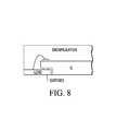
- FIG. 8is a cross section of a portion of an alternative semiconductor device to the semiconductor device as shown in FIG. 3 .
- a semiconductor devicein one aspect, includes a semiconductor die having a bottom edge with a notch that allows a lead of a lead frame to fit in the notch. This reduces the increase in height that occurs when a lead frame is placed under the semiconductor device.
- FIG. 1Shown in FIG. 1 is a semiconductor device 10 having a semiconductor die 12 having an active side 28 and a backside 30 , which are the major surfaces 28 and 30 of semiconductor die 12 .
- Die 12may include a plurality of substrate layers. Active side 28 is also the top side in this example.
- Semiconductor die 12has contact pads 14 and 16 on active side 28 , a notch 18 along a first edge 11 of backside 30 , and a notch 20 along a second edge 13 of backside 30 .
- the first and second edges 11 and 13may be considered minor surfaces 11 and 13 of semiconductor die 12 .
- Notch 18may be one a plurality of notches along the first edge in one configuration and may extend the length of the first edge in a second configuration.
- Notch 18has an endwall 19 which is the extent that notch 18 extends from first outer edge 11 of semiconductor die 12 . This is shown as length 22 . Depth of notch 18 is measured from backside 30 and is shown as depth 24 . Notch 20 has an endwall 21 . Notch 20 may have the same length and depth as notch 18 . Semiconductor die 12 has a thickness 26 . Depth 24 must be sufficiently less than thickness 26 to avoid excessive risk of damage to semiconductor die 12 in the various processes required to achieve a finished package die.
- FIG. 2Shown in FIG. 2 is semiconductor device 10 after semiconductor die 12 is placed on a lead frame having a plurality of leads such as leads 32 and 34 .
- leads 32 and 34This has the effect of an end portion of lead 32 being in notch 18 , an end portion of a lead 34 being in notch 20 , a top surface of the end portion of lead 32 being attached to a top surface of notch 18 with an adhesive 36 , and a top surface of the end portion of lead 34 being attached to a top surface of notch 20 with an adhesive 38 .
- Adhesives 36 and 38hold leads 32 and 34 in place during assembly in preparation for encapsulation.
- a bottom surface 33 of lead 32 and a bottom surface 35 of lead 34may preferably be above the surface of backside 30 .
- the thickness of leads 32 and 34is less than depth 24 by enough to accommodate adhesives 36 and 38 and still be recessed to avoid coplanarity with the surface of backside 30 .
- a thickness of the leadmeasured in a same direction as the notch depth, may be at least 80% of the notch depth.
- the notch lengthmay be at least 25 micrometers.
- Adhesives currently in use for attaching semiconductor die to lead framesmay be used as adhesives 36 and 38 . As an alternative, adhesives 36 and 38 may not be required at this stage. Some benefit can still be obtained if leads 32 and 34 have some portion below the surface of backside 30 .
- leads 32 and 34may be coplanar with the surface of backside 30 and exposed which is the approach in a package type known as QFN and shown in FIG. 8 .
- leads 32 and 34are shown as being uniform in thickness but they may vary. For example, they may be thinned where they enter notches 18 and 20 .
- FIG. 3Shown in FIG. 3 is semiconductor device 10 after a wirebond 40 is connected on one end to lead 32 and on another end to contact pad 14 and a wirebond 42 is connected on one end to lead 34 and on another end to contact pad 16 .
- Leads 32 and 34are thicker than contact pads 14 and 16 but thinner than the length of endwalls 19 and 21 so that leads 32 and 34 do not extend below bottom surface 30 .
- FIG. 4Shown in FIG. 4 is semiconductor device 10 after encapsulating semiconductor die 12 , wirebonds 40 and 42 , and portions of leads 32 and 34 including portions of bottom surfaces 33 and 35 as well as filling in notches 18 and 20 with an encapsulant 44 .
- the bottom surface of encapsulant 44is coplanar with the surface of backside 30 .
- Semiconductor device 10 of FIG. 4shows a completed packaged die. Bottom surface 30 is exposed which is excellent for attaching heat dissipating structures to semiconductor die 12 .
- leads 32 and 34do not contribute to the total height of semiconductor device 10 . The total height is just from surface of backside 30 to the top surface of encapsulant 44 .
- leads 32 and 34extend only partially below bottom surface 30 , there is still a benefit of a reduction in height of an amount equal to the extent to which leads 32 and 34 extend into notches 18 and 20 .
- FIG. 5Shown in FIG. 5 is semiconductor device 10 of FIG. 3 , in a first configuration, viewed toward backside 30 .
- this first configurationthere are plurality 50 of notches along minor surface 11 , including notch 18 , and a plurality 52 of notches along minor surface 13 , including notch 20 .
- each leadhas its own notch and each notch has sidewalls.
- notch 18has a sidewall 46
- notch 20has a sidewall 48 .
- the other two minor surfacescould also have pluralities of notches with leads. Also this shows one lead per notch, but the notches could be extended to receive more than one lead. For example, there could be two leads per notch.
- FIG. 6Shown in FIG. 6 , in isometric form, is a portion of semiconductor device 10 of FIG. 1 , in a second configuration viewed with edge 11 in front and backside 30 on top. This shows that notch 18 extends for the length of edge 11 . All of the leads, for a given edge, in this second configuration would in the same notch. The spacing of the leads would be achieved by proper placement of the leads and held by adhesives such as adhesives 36 and 38 . Depth 24 and length 22 are shown which define the length and depth of notch 18 . Notch 20 would be on the opposing edge which is edge 13 . The other two minor surfaces could also have notches, like notch 18 shown in FIG. 6 , that span the length of the minor surfaces.
- FIG. 7Shown in isometric form, is a portion of semiconductor device 10 of FIG. 1 , in the first configuration viewed from edge 11 and backside 30 . This shows three notches of plurality of notches 50 including notch 18 . Shown also are length 22 and depth 24 . Plurality of notches, similar to notches 50 , could be on the other minor surfaces.
- thiscan be achieved by first etching a channel between semiconductor die on a wafer that has a depth of depth 24 and a length across the channel sufficient to result in length 22 after singulation.
- thiscan be performed as a patterned etch performed as part of the wafer fabrication process that will result in the desired length 22 and depth 24 after singulation.
- Other techniquesinclude using a grinder or a laser to achieve the desired length 22 and depth 24 after singulation.
- a semiconductor devicehaving a semiconductor die having a first major surface and a second major surface opposite the first major surface, a first minor surface and a second minor surface opposite the first minor surface, wherein the first and second minor surfaces are between the first and second major surfaces, a plurality of contact pads on the first major surface, and a notch which extends from the first minor surface and the second major surface into the semiconductor die.
- the semiconductor diehas a further characterization by which the notch has a notch depth measured from the second major surface into the semiconductor die, wherein the notch depth is less than a thickness of the semiconductor die, and a notch length measured from the first minor surface into the semiconductor die, wherein the notch length is less than a length of the semiconductor die measured between the first and second minor surfaces . . . .
- the semiconductor devicefurther includes a lead having a first end in the notch.
- the semiconductor devicefurther includes an encapsulant over the first major surface of the semiconductor die.
- the semiconductor devicemay have a further characterization by which the encapsulant extends into the notch.
- the semiconductor devicemay further include a wire bond connected between a contact pad of the plurality of contact pads and the lead, wherein the encapsulant is over the wire bond.
- the semiconductor devicemay further include an adhesive in the notch between the lead and the semiconductor die.
- the semiconductor devicemay have a further characterization by which the semiconductor die has a third minor surface and a fourth minor surface opposite the third minor surface, wherein the third and four minor surfaces are substantially perpendicular to the first and second minor surfaces, and wherein the notch extends through the semiconductor die from the third minor surface to the fourth minor surface.
- the semiconductor devicemay have a further characterization by which the notch is one of a plurality of notches, wherein each of the plurality of notches extends from the first minor surface and the second major surface into the semiconductor die, and wherein each notch of the plurality of notches has a notch depth less than the thickness of the semiconductor die and a notch length less than the length of the semiconductor die.
- the semiconductor devicemay have a further characterization by which the lead is one of a plurality of leads, and wherein each of the plurality of notches includes a first end of one or more leads of the plurality of leads.
- the semiconductor devicemay have a further characterization by which each notch of the plurality of notches has a same notch length and a same notch depth.
- the semiconductor devicemay have a further characterization by which a thickness of the lead, measured in a same direction as the notch depth, is at least 80% of the notch depth.
- the semiconductor devicemay have a further characterization by which the notch length is at least 25 micrometers.
- the semiconductor devicemay have a further characterization by which at least a portion of the second major surface is exposed.
- the semiconductor devicemay have a further characterization by which the semiconductor die comprises a plurality of substrate layers.
- a method for forming a semiconductor devicethat includes forming a notch in a semiconductor die having a first major surface, a second major surface opposite the first major surface, a first minor surface, a second minor surface opposite the first minor surface, and a plurality of contact pads on the first major surface.
- the notchextends from the first minor surface and the second major surface into the semiconductor die.
- the notchfurther has a notch depth measured from the second major surface into the semiconductor die, wherein the notch depth is less than a thickness of the semiconductor die, and a notch length measured from the first minor surface into the semiconductor die, wherein the notch length is less than a length of the semiconductor die measured between the first and second minor surfaces.
- the methodfurther includes placing a first end of a lead into the notch.
- the methodfurther includes forming an encapsulant over the first major surface of the semiconductor die.
- the methodhas a further characterization by which forming the encapsulant is performed such that the encapsulant extends into the notch.
- the methodfurther includes forming a wire bond connection between a contact pad of the plurality of contact pads and the lead, wherein the encapsulant is over the wire bond connection.
- the methodhas a further characterization by which the placing the first end of the lead into the notch comprises attaching the first end to the semiconductor die with an adhesive.
- the methodhas a further characterization by which wherein the semiconductor die has a third minor surface and a fourth minor surface opposite the third minor surface, wherein the third and four minor surfaces are substantially perpendicular to the first and second minor surfaces, and wherein forming the notch extends through the semiconductor die from the third minor surface to the fourth minor surface.
- the methodhas a further characterization by which forming the notch comprises forming a plurality of notches, wherein each of the plurality of notches extends from the first minor surface and the second major surface into the semiconductor die, and wherein each notch of the plurality of notches has a notch depth less than the thickness of the semiconductor die and a notch length less than the length of the semiconductor die.
- placing the leadcomprises placing a first end of one or more leads of a plurality of leads into each notch of the plurality of notches.
- a semiconductor devicehaving a semiconductor die having a first major surface and a second major surface, opposite the first major surface, a first minor surface and a second minor surface, opposite the first minor surface, a third minor surface and a fourth minor surface, opposite the third minor surface, wherein the first, second, third, and fourth minor surfaces are between the first and second major surfaces, a plurality of contact pads on the first major surface, and a notch which extends from the first minor surface and the second major surface into the semiconductor die and which extends through the semiconductor die from the third minor surface to the fourth minor surface.
- the semiconductorhas a further characterization by which the notch has a notch depth measured from the second major surface into the semiconductor die, wherein the notch depth is less than a thickness of the semiconductor die.
- the semiconductor devicefurther includes a plurality of leads, each having a first end in the notch.
- the semiconductor devicefurther includes a plurality of wire bonds, each connected between a contact pad of the plurality of contact pads and a corresponding lead of the plurality of leads.
- the semiconductor devicefurther includes an encapsulant over the plurality of wire bonds and over the first major surface of the semiconductor die.
Landscapes
- Engineering & Computer Science (AREA)
- Microelectronics & Electronic Packaging (AREA)
- Computer Hardware Design (AREA)
- Power Engineering (AREA)
- Physics & Mathematics (AREA)
- Condensed Matter Physics & Semiconductors (AREA)
- General Physics & Mathematics (AREA)
- Lead Frames For Integrated Circuits (AREA)
Abstract
Description
Claims (20)
Priority Applications (1)
| Application Number | Priority Date | Filing Date | Title |
|---|---|---|---|
| US13/935,015US8957510B2 (en) | 2013-07-03 | 2013-07-03 | Using an integrated circuit die configuration for package height reduction |
Applications Claiming Priority (1)
| Application Number | Priority Date | Filing Date | Title |
|---|---|---|---|
| US13/935,015US8957510B2 (en) | 2013-07-03 | 2013-07-03 | Using an integrated circuit die configuration for package height reduction |
Publications (2)
| Publication Number | Publication Date |
|---|---|
| US20150008567A1 US20150008567A1 (en) | 2015-01-08 |
| US8957510B2true US8957510B2 (en) | 2015-02-17 |
Family
ID=52132236
Family Applications (1)
| Application Number | Title | Priority Date | Filing Date |
|---|---|---|---|
| US13/935,015ActiveUS8957510B2 (en) | 2013-07-03 | 2013-07-03 | Using an integrated circuit die configuration for package height reduction |
Country Status (1)
| Country | Link |
|---|---|
| US (1) | US8957510B2 (en) |
Families Citing this family (3)
| Publication number | Priority date | Publication date | Assignee | Title |
|---|---|---|---|---|
| TWI559576B (en)* | 2013-11-05 | 2016-11-21 | Sfi Electronics Technology Inc | A chip type diode package element and its manufacturing method |
| US10412749B2 (en)* | 2015-05-21 | 2019-09-10 | Telefonaktiebolaget Lm Ericsson (Publ) | Scheduling in license assisted access |
| US9875993B2 (en)* | 2016-01-14 | 2018-01-23 | Micron Technology, Inc. | Semiconductor devices with duplicated die bond pads and associated device packages and methods of manufacture |
Citations (13)
| Publication number | Priority date | Publication date | Assignee | Title |
|---|---|---|---|---|
| US5195023A (en) | 1991-12-23 | 1993-03-16 | At&T Bell Laboratories | Integrated circuit package with strain relief grooves |
| US5455200A (en) | 1992-02-03 | 1995-10-03 | Motorola, Inc. | Method for making a lead-on-chip semiconductor device having peripheral bond pads |
| US5696666A (en) | 1995-10-11 | 1997-12-09 | Motorola, Inc. | Low profile exposed die chip carrier package |
| US6201186B1 (en) | 1998-06-29 | 2001-03-13 | Motorola, Inc. | Electronic component assembly and method of making the same |
| US6664649B2 (en) | 2001-02-28 | 2003-12-16 | Siliconware Precision Industries Co., Ltd. | Lead-on-chip type of semiconductor package with embedded heat sink |
| US20060220241A1 (en)* | 2001-08-01 | 2006-10-05 | Neill Thornton | Packaged semiconductor device and method of manufacture using shaped die |
| US20080211090A1 (en)* | 2005-07-05 | 2008-09-04 | Koninklijke Philips Electronics, N.V. | Packed Semiconductor Sensor Chip For Use In Liquids |
| US20080237887A1 (en) | 2007-03-29 | 2008-10-02 | Hem Takiar | Semiconductor die stack having heightened contact for wire bond |
| US20090026592A1 (en)* | 2007-07-24 | 2009-01-29 | Micron Technology, Inc. | Semiconductor dies with recesses, associated leadframes, and associated systems and methods |
| US20090045491A1 (en)* | 2007-08-15 | 2009-02-19 | Advanced Semiconductor Engineering, Inc. | Semiconductor package structure and leadframe thereof |
| US7713781B2 (en) | 2006-10-31 | 2010-05-11 | Freescale Semiconductor, Inc. | Methods for forming quad flat no-lead (QFN) packages |
| US20100327421A1 (en) | 2009-06-30 | 2010-12-30 | Stmicroelectronics Asia Pacific Pte. Ltd. | Ic package design with stress relief feature |
| US20110057296A1 (en)* | 2009-09-08 | 2011-03-10 | Texas Instruments Incorporated | Delamination resistant packaged die having support and shaped die having protruding lip on support |
- 2013
- 2013-07-03USUS13/935,015patent/US8957510B2/enactiveActive
Patent Citations (13)
| Publication number | Priority date | Publication date | Assignee | Title |
|---|---|---|---|---|
| US5195023A (en) | 1991-12-23 | 1993-03-16 | At&T Bell Laboratories | Integrated circuit package with strain relief grooves |
| US5455200A (en) | 1992-02-03 | 1995-10-03 | Motorola, Inc. | Method for making a lead-on-chip semiconductor device having peripheral bond pads |
| US5696666A (en) | 1995-10-11 | 1997-12-09 | Motorola, Inc. | Low profile exposed die chip carrier package |
| US6201186B1 (en) | 1998-06-29 | 2001-03-13 | Motorola, Inc. | Electronic component assembly and method of making the same |
| US6664649B2 (en) | 2001-02-28 | 2003-12-16 | Siliconware Precision Industries Co., Ltd. | Lead-on-chip type of semiconductor package with embedded heat sink |
| US20060220241A1 (en)* | 2001-08-01 | 2006-10-05 | Neill Thornton | Packaged semiconductor device and method of manufacture using shaped die |
| US20080211090A1 (en)* | 2005-07-05 | 2008-09-04 | Koninklijke Philips Electronics, N.V. | Packed Semiconductor Sensor Chip For Use In Liquids |
| US7713781B2 (en) | 2006-10-31 | 2010-05-11 | Freescale Semiconductor, Inc. | Methods for forming quad flat no-lead (QFN) packages |
| US20080237887A1 (en) | 2007-03-29 | 2008-10-02 | Hem Takiar | Semiconductor die stack having heightened contact for wire bond |
| US20090026592A1 (en)* | 2007-07-24 | 2009-01-29 | Micron Technology, Inc. | Semiconductor dies with recesses, associated leadframes, and associated systems and methods |
| US20090045491A1 (en)* | 2007-08-15 | 2009-02-19 | Advanced Semiconductor Engineering, Inc. | Semiconductor package structure and leadframe thereof |
| US20100327421A1 (en) | 2009-06-30 | 2010-12-30 | Stmicroelectronics Asia Pacific Pte. Ltd. | Ic package design with stress relief feature |
| US20110057296A1 (en)* | 2009-09-08 | 2011-03-10 | Texas Instruments Incorporated | Delamination resistant packaged die having support and shaped die having protruding lip on support |
Non-Patent Citations (1)
| Title |
|---|
| Lassig, S., "Manufacturing integration considerations of through-silicon via etching", Solid State Technology, Insights for Electronics Manufacturing, Dec. 1, 2007. |
Also Published As
| Publication number | Publication date |
|---|---|
| US20150008567A1 (en) | 2015-01-08 |
Similar Documents
| Publication | Publication Date | Title |
|---|---|---|
| TWI474455B (en) | Advanced quad flat no-lead package | |
| US6617197B1 (en) | Multi row leadless leadframe package | |
| US10109561B2 (en) | Semiconductor device having plated outer leads exposed from encapsulating resin | |
| US9698064B2 (en) | Semiconductor device having semiconductor chip mounted on lead frame | |
| CN204834611U (en) | Lead frame and unit, semiconductor package structure and unit thereof | |
| US20080150106A1 (en) | Inverted lf in substrate | |
| US9620388B2 (en) | Integrated circuit package fabrication with die attach paddle having middle channels | |
| US8957510B2 (en) | Using an integrated circuit die configuration for package height reduction | |
| US9786583B2 (en) | Power semiconductor package device having locking mechanism, and preparation method thereof | |
| TWI431728B (en) | Semiconductor package with reinforced base | |
| US7498665B2 (en) | Integrated circuit leadless package system | |
| US20150054145A1 (en) | Integrated circuit package with die attach paddle having at least one recessed portion | |
| CN113192920B (en) | A pin structure of QFN package | |
| CN101740416A (en) | Quad flat no-lead encapsulation structure and encapsulation method thereof | |
| US20140264793A1 (en) | Lead frame for semiconductor package with enhanced stress relief | |
| CN205004326U (en) | Integrated circuit device | |
| US8643156B2 (en) | Lead frame for assembling semiconductor device | |
| CN212209475U (en) | Lead frame and package | |
| US8080444B2 (en) | Method for forming a packaged semiconductor device having a ground plane | |
| CN100470782C (en) | Chip package structure | |
| CN101826499A (en) | Quad flat non-leaded package | |
| US20080093719A1 (en) | Chip package structure | |
| TW201309126A (en) | Memory card package having a small substrate | |
| US10468336B2 (en) | High density semiconductor package and related methods | |
| CN202120898U (en) | Semiconductor packaging structure |
Legal Events
| Date | Code | Title | Description |
|---|---|---|---|
| AS | Assignment | Owner name:FREESCALE SEMICONDUCTOR, INC., TEXAS Free format text:ASSIGNMENT OF ASSIGNORS INTEREST;ASSIGNORS:PHAM, TIM V.;GUAJARDO, JAMES R.;MCSHANE, MICHAEL B.;REEL/FRAME:030737/0902 Effective date:20130626 | |
| AS | Assignment | Owner name:CITIBANK, N.A., AS NOTES COLLATERAL AGENT, NEW YORK Free format text:SECURITY AGREEMENT;ASSIGNOR:FREESCALE SEMICONDUCTOR, INC.;REEL/FRAME:031591/0266 Effective date:20131101 Owner name:CITIBANK, N.A., AS NOTES COLLATERAL AGENT, NEW YOR Free format text:SECURITY AGREEMENT;ASSIGNOR:FREESCALE SEMICONDUCTOR, INC.;REEL/FRAME:031591/0266 Effective date:20131101 | |
| AS | Assignment | Owner name:CITIBANK, N.A., AS NOTES COLLATERAL AGENT, NEW YOR Free format text:SUPPLEMENT TO IP SECURITY AGREEMENT;ASSIGNOR:FREESCALE SEMICONDUCTOR, INC.;REEL/FRAME:031627/0201 Effective date:20131101 Owner name:CITIBANK, N.A., AS COLLATERAL AGENT, NEW YORK Free format text:SUPPLEMENT TO IP SECURITY AGREEMENT;ASSIGNOR:FREESCALE SEMICONDUCTOR, INC.;REEL/FRAME:031627/0158 Effective date:20131101 | |
| STCF | Information on status: patent grant | Free format text:PATENTED CASE | |
| AS | Assignment | Owner name:FREESCALE SEMICONDUCTOR, INC., TEXAS Free format text:PATENT RELEASE;ASSIGNOR:CITIBANK, N.A., AS COLLATERAL AGENT;REEL/FRAME:037357/0874 Effective date:20151207 | |
| AS | Assignment | Owner name:MORGAN STANLEY SENIOR FUNDING, INC., MARYLAND Free format text:ASSIGNMENT AND ASSUMPTION OF SECURITY INTEREST IN PATENTS;ASSIGNOR:CITIBANK, N.A.;REEL/FRAME:037444/0787 Effective date:20151207 | |
| AS | Assignment | Owner name:MORGAN STANLEY SENIOR FUNDING, INC., MARYLAND Free format text:ASSIGNMENT AND ASSUMPTION OF SECURITY INTEREST IN PATENTS;ASSIGNOR:CITIBANK, N.A.;REEL/FRAME:037518/0292 Effective date:20151207 | |
| AS | Assignment | Owner name:MORGAN STANLEY SENIOR FUNDING, INC., MARYLAND Free format text:SUPPLEMENT TO THE SECURITY AGREEMENT;ASSIGNOR:FREESCALE SEMICONDUCTOR, INC.;REEL/FRAME:039138/0001 Effective date:20160525 | |
| AS | Assignment | Owner name:NXP, B.V., F/K/A FREESCALE SEMICONDUCTOR, INC., NETHERLANDS Free format text:RELEASE BY SECURED PARTY;ASSIGNOR:MORGAN STANLEY SENIOR FUNDING, INC.;REEL/FRAME:040925/0001 Effective date:20160912 Owner name:NXP, B.V., F/K/A FREESCALE SEMICONDUCTOR, INC., NE Free format text:RELEASE BY SECURED PARTY;ASSIGNOR:MORGAN STANLEY SENIOR FUNDING, INC.;REEL/FRAME:040925/0001 Effective date:20160912 | |
| AS | Assignment | Owner name:MORGAN STANLEY SENIOR FUNDING, INC., MARYLAND Free format text:CORRECTIVE ASSIGNMENT TO CORRECT THE INCORRECT PCT NUMBERS IB2013000664, US2013051970, US201305935 PREVIOUSLY RECORDED AT REEL: 037444 FRAME: 0787. ASSIGNOR(S) HEREBY CONFIRMS THE ASSIGNMENT AND ASSUMPTION OF SECURITY INTEREST IN PATENTS;ASSIGNOR:CITIBANK, N.A.;REEL/FRAME:040450/0715 Effective date:20151207 | |
| AS | Assignment | Owner name:NXP B.V., NETHERLANDS Free format text:RELEASE BY SECURED PARTY;ASSIGNOR:MORGAN STANLEY SENIOR FUNDING, INC.;REEL/FRAME:040928/0001 Effective date:20160622 | |
| AS | Assignment | Owner name:NXP USA, INC., TEXAS Free format text:MERGER;ASSIGNOR:FREESCALE SEMICONDUCTOR, INC.;REEL/FRAME:041144/0363 Effective date:20161107 | |
| AS | Assignment | Owner name:MORGAN STANLEY SENIOR FUNDING, INC., MARYLAND Free format text:CORRECTIVE ASSIGNMENT TO CORRECT THE REMOVE PATENTS 8108266 AND 8062324 AND REPLACE THEM WITH 6108266 AND 8060324 PREVIOUSLY RECORDED ON REEL 037518 FRAME 0292. ASSIGNOR(S) HEREBY CONFIRMS THE ASSIGNMENT AND ASSUMPTION OF SECURITY INTEREST IN PATENTS;ASSIGNOR:CITIBANK, N.A.;REEL/FRAME:041703/0536 Effective date:20151207 | |
| MAFP | Maintenance fee payment | Free format text:PAYMENT OF MAINTENANCE FEE, 4TH YEAR, LARGE ENTITY (ORIGINAL EVENT CODE: M1551) Year of fee payment:4 | |
| AS | Assignment | Owner name:SHENZHEN XINGUODU TECHNOLOGY CO., LTD., CHINA Free format text:CORRECTIVE ASSIGNMENT TO CORRECT THE TO CORRECT THE APPLICATION NO. FROM 13,883,290 TO 13,833,290 PREVIOUSLY RECORDED ON REEL 041703 FRAME 0536. ASSIGNOR(S) HEREBY CONFIRMS THE THE ASSIGNMENT AND ASSUMPTION OF SECURITYINTEREST IN PATENTS.;ASSIGNOR:MORGAN STANLEY SENIOR FUNDING, INC.;REEL/FRAME:048734/0001 Effective date:20190217 | |
| AS | Assignment | Owner name:NXP B.V., NETHERLANDS Free format text:RELEASE BY SECURED PARTY;ASSIGNOR:MORGAN STANLEY SENIOR FUNDING, INC.;REEL/FRAME:050744/0097 Effective date:20190903 | |
| AS | Assignment | Owner name:NXP B.V., NETHERLANDS Free format text:CORRECTIVE ASSIGNMENT TO CORRECT THE REMOVEAPPLICATION 11759915 AND REPLACE IT WITH APPLICATION11759935 PREVIOUSLY RECORDED ON REEL 040928 FRAME 0001. ASSIGNOR(S) HEREBY CONFIRMS THE RELEASE OF SECURITYINTEREST;ASSIGNOR:MORGAN STANLEY SENIOR FUNDING, INC.;REEL/FRAME:052915/0001 Effective date:20160622 | |
| AS | Assignment | Owner name:NXP, B.V. F/K/A FREESCALE SEMICONDUCTOR, INC., NETHERLANDS Free format text:CORRECTIVE ASSIGNMENT TO CORRECT THE REMOVEAPPLICATION 11759915 AND REPLACE IT WITH APPLICATION11759935 PREVIOUSLY RECORDED ON REEL 040925 FRAME 0001. ASSIGNOR(S) HEREBY CONFIRMS THE RELEASE OF SECURITYINTEREST;ASSIGNOR:MORGAN STANLEY SENIOR FUNDING, INC.;REEL/FRAME:052917/0001 Effective date:20160912 | |
| MAFP | Maintenance fee payment | Free format text:PAYMENT OF MAINTENANCE FEE, 8TH YEAR, LARGE ENTITY (ORIGINAL EVENT CODE: M1552); ENTITY STATUS OF PATENT OWNER: LARGE ENTITY Year of fee payment:8 |