US8954001B2 - Power bridge circuit for bi-directional wireless power transmission - Google Patents
Power bridge circuit for bi-directional wireless power transmissionDownload PDFInfo
- Publication number
- US8954001B2 US8954001B2US12/628,401US62840109AUS8954001B2US 8954001 B2US8954001 B2US 8954001B2US 62840109 AUS62840109 AUS 62840109AUS 8954001 B2US8954001 B2US 8954001B2
- Authority
- US
- United States
- Prior art keywords
- power
- signal interface
- inductive
- inductive signal
- bridge circuit
- Prior art date
- Legal status (The legal status is an assumption and is not a legal conclusion. Google has not performed a legal analysis and makes no representation as to the accuracy of the status listed.)
- Active, expires
Links
- 230000005540biological transmissionEffects0.000titleclaimsdescription6
- 230000001939inductive effectEffects0.000claimsabstractdescription244
- 239000003990capacitorSubstances0.000claimsdescription34
- 238000004891communicationMethods0.000claimsdescription28
- 238000012546transferMethods0.000claimsdescription16
- 238000003032molecular dockingMethods0.000claimsdescription7
- 230000001360synchronised effectEffects0.000claimsdescription6
- 230000001413cellular effectEffects0.000description4
- 238000010586diagramMethods0.000description4
- 238000002955isolationMethods0.000description4
- 238000000034methodMethods0.000description3
- 238000012545processingMethods0.000description3
- 230000008901benefitEffects0.000description2
- 230000033228biological regulationEffects0.000description2
- 230000003750conditioning effectEffects0.000description2
- 230000006870functionEffects0.000description2
- 230000014759maintenance of locationEffects0.000description2
- 238000004519manufacturing processMethods0.000description2
- 230000008569processEffects0.000description2
- 230000001105regulatory effectEffects0.000description2
- 239000000523sampleSubstances0.000description2
- CWYNVVGOOAEACU-UHFFFAOYSA-NFe2+Chemical compound[Fe+2]CWYNVVGOOAEACU-UHFFFAOYSA-N0.000description1
- 241001071864Lethrinus laticaudisSpecies0.000description1
- 230000000712assemblyEffects0.000description1
- 238000000429assemblyMethods0.000description1
- 230000015572biosynthetic processEffects0.000description1
- 230000008859changeEffects0.000description1
- 238000006243chemical reactionMethods0.000description1
- 239000004020conductorSubstances0.000description1
- 239000000463materialSubstances0.000description1
- 238000012986modificationMethods0.000description1
- 230000004048modificationEffects0.000description1
- 230000010363phase shiftEffects0.000description1
- 230000004044responseEffects0.000description1
- 230000000717retained effectEffects0.000description1
- 230000011664signalingEffects0.000description1
Images


Classifications
- H02J5/005—
- H—ELECTRICITY
- H02—GENERATION; CONVERSION OR DISTRIBUTION OF ELECTRIC POWER
- H02J—CIRCUIT ARRANGEMENTS OR SYSTEMS FOR SUPPLYING OR DISTRIBUTING ELECTRIC POWER; SYSTEMS FOR STORING ELECTRIC ENERGY
- H02J50/00—Circuit arrangements or systems for wireless supply or distribution of electric power
- H02J50/40—Circuit arrangements or systems for wireless supply or distribution of electric power using two or more transmitting or receiving devices
- H02J50/402—Circuit arrangements or systems for wireless supply or distribution of electric power using two or more transmitting or receiving devices the two or more transmitting or the two or more receiving devices being integrated in the same unit, e.g. power mats with several coils or antennas with several sub-antennas
- H—ELECTRICITY
- H02—GENERATION; CONVERSION OR DISTRIBUTION OF ELECTRIC POWER
- H02J—CIRCUIT ARRANGEMENTS OR SYSTEMS FOR SUPPLYING OR DISTRIBUTING ELECTRIC POWER; SYSTEMS FOR STORING ELECTRIC ENERGY
- H02J50/00—Circuit arrangements or systems for wireless supply or distribution of electric power
- H02J50/10—Circuit arrangements or systems for wireless supply or distribution of electric power using inductive coupling
- H02J50/12—Circuit arrangements or systems for wireless supply or distribution of electric power using inductive coupling of the resonant type
- H—ELECTRICITY
- H02—GENERATION; CONVERSION OR DISTRIBUTION OF ELECTRIC POWER
- H02J—CIRCUIT ARRANGEMENTS OR SYSTEMS FOR SUPPLYING OR DISTRIBUTING ELECTRIC POWER; SYSTEMS FOR STORING ELECTRIC ENERGY
- H02J50/00—Circuit arrangements or systems for wireless supply or distribution of electric power
- H02J50/80—Circuit arrangements or systems for wireless supply or distribution of electric power involving the exchange of data, concerning supply or distribution of electric power, between transmitting devices and receiving devices
- H—ELECTRICITY
- H02—GENERATION; CONVERSION OR DISTRIBUTION OF ELECTRIC POWER
- H02J—CIRCUIT ARRANGEMENTS OR SYSTEMS FOR SUPPLYING OR DISTRIBUTING ELECTRIC POWER; SYSTEMS FOR STORING ELECTRIC ENERGY
- H02J7/00—Circuit arrangements for charging or depolarising batteries or for supplying loads from batteries
- H02J7/0047—Circuit arrangements for charging or depolarising batteries or for supplying loads from batteries with monitoring or indicating devices or circuits
- H02J7/0048—Detection of remaining charge capacity or state of charge [SOC]
Definitions
- the disclosed embodimentsrelate generally to the field of inductive signal interfaces.
- the disclosed embodimentsrelate to an inductive signal interface capable of bi-directional inductive signaling.
- FIG. 1illustrates an H-bridge inverter circuit 110 for transferring power from a DC supply 120 to an AC load 115 .
- the H-bridge inverter circuit 110includes four switches 111 - 114 each controlled by a respective one of control signals H 1 -H 4 .
- the switches 111 - 114turn on and off in pairs to deliver an AC current to the AC load 115 .
- the signals H 1 and H 4are asserted to turn on switches 111 and 114
- the signals H 2 and H 3are de-asserted to turn off the switches 112 and 113 .
- the H-bridge inverteris configured to deliver an AC current from the DC supply 120 to the AC load 115 .
- FIG. 2illustrates a sync bridge circuit 210 for transferring power from an AC supply 215 to a DC load 220 .
- the sync bridge circuit 210includes four switches 211 - 214 each controlled by a respective one of control signals S 1 -S 4 .
- the sync bridge circuit 210receives an AC current from the AC supply 215 , and the switches 211 - 214 of the sync bridge circuit 210 turn on and off in pairs to deliver a DC current to the DC load.
- FIG. 1illustrates a prior art H-bridge inverter circuit for delivering power from a DC power supply to an AC load.
- FIG. 2illustrates a prior art synchronous bridge rectifier circuit for delivering power from an AC power supply to a DC load.
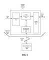
- FIG. 3is a block diagram illustrating an inductive signal interface, according to one or more embodiments.
- FIG. 4illustrates an inductive signal interface capable of performing data transfer through an inductive link, under another embodiment.
- FIG. 5illustrates an inductive signal interface capable of performing inductive data transfer, under another embodiment.
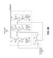
- FIG. 6Aillustrates circuit level embodiments of the power bridge and the bi-directional coil assembly.
- FIG. 6Bis illustrates the power bridge circuit of FIG. 6A coupled to another bi-directional coil assembly, under another embodiment.
- FIG. 6Cillustrates the power bridge circuit of FIG. 6A coupled to a bi-directional coil assembly, under another embodiment.
- FIG. 6Dillustrates the power bridge circuit of FIG. 6A coupled to a bi-directional coil assembly, under another embodiment.
- FIG. 7Aillustrates an embodiment of a bi-directional coil assembly.
- FIG. 7Billustrates a current path within the inductive coil assembly of FIG. 7A during a power receive mode.
- FIG. 7Cillustrates a current path within the inductive coil assembly of FIG. 7A during the power transmit mode.
- FIG. 7Dillustrates another embodiment of the bi-directional coil assembly.
- FIG. 7Eillustrates a current path within the inductive coil assembly of FIG. 7D during the power receive mode.
- FIG. 7Fillustrates a current path within the inductive coil assembly of FIG. 7D during the power transmit mode.
- FIG. 8Aillustrates an operation of an embodiment of the power bridge circuit in the power transmit mode.
- FIG. 8Billustrates another operation of an embodiment of the power bridge circuit in the power transmit mode.
- FIG. 8Cillustrates an operation of an embodiment of the power bridge circuit in the power receive mode.
- FIG. 8Dillustrates another operation of an embodiment of the power bridge circuit in the power receive mode.
- FIG. 8Eillustrates another embodiment that includes consideration of a flying node, under an embodiment.
- FIG. 9illustrates the combination two similarly structured computing devices, each using a “3-legged” power bridge circuit, according to one or more embodiments.
- FIG. 10illustrates a power bridge circuit and a bi-directional coil assembly coupled to current conditioning circuitry, according to another embodiment.
- FIG. 11is a representative diagram illustrating two computing devices that can be brought into contact for purpose of enabling one device to provide a power and/or data signal to the other device, according to one or more embodiments.
- Embodiments described hereininclude an inductive signal interface that uses shared circuit elements to be operable as either a power transmitter or a power receiver. More specifically, an inductive signal interface includes a three-legged (or three-branched) structure that uses separate pairs of legs or branches to operate as an inductive power transmitter or an inductive power receiver.
- An inductive signal interfaceincludes a coil assembly which has one or more inductive coils.
- the inductive signal interfacealso has a bridge circuit that couples to the coil assembly to a power input/output (I/O).
- the bridge circuithas components that operate to enable the inductive signal interface to selectively operate in either a power transmit mode or a power receive mode.
- the selective operation of the inductive signal interfacemay be determined: (i) in real-time based on, for example, an identification or mode of operation of the type of the other coupled device, and/or (ii) at a time of manufacturing based on the power consumption and/or transmission capabilities of the manufactured device.
- bridge circuitsare circuits having at least two parallel current paths that form an enclosed loop.
- a bridge circuitis a circuit that has multiple current branches that are individually operable to enable current to pass one direction or in a reverse direction.
- a computing systemthat includes a first and a second computing devices, each computing device including a similarly structured inductive signal interface.
- the inductive signal interface of each computing deviceincludes a coil assembly which has one or more inductive coils and a bridge circuit that couples to the coil assembly to a power input/output (I/O).
- Each bridge circuithas components that operate to enable the respective inductive signal interface to selectively operate in either a power transmit mode or a power receive mode.
- FIG. 3is a block diagram illustrating an embodiment of an inductive signal interface.
- an inductive signal interface 310includes a power bridge circuit 311 , a bi-directional coil assembly 312 , a control circuit 313 , and a power circuit 314 .
- the inductive signal interface 310may reside on any device that is capable of inductively receiving or transmitting power with another suitably configured device. Such devices are described in detail in U.S. patent application Ser. No. 12/478,766 entitled “Inductive Signal Transfer System for Computing Devices,” (which is hereby incorporated by reference in its entirety).
- an inductive signal interface 310may be integrated or incorporated into a mobile computing device (such as in a cellular telephony/messaging device), mobile computing device housing or housing accessory (e.g. housing panel for mobile computing device) or docking station.
- the inductive signal interface 310resides in a inductive charger for the mobile device.
- a device having inductive signal interface 310may be referenced as an ‘electronic device’, and correspond to, for example, a mobile computing device or docking station.
- the inductive signal interface 310is shown in FIG. 1 to be provided on a first electronic device 302 , and used to create an inductive link 330 with a second electronic device 320 .
- the second electronic device 320may be any device capable of inductively receiving or transmitting signals.
- the first electronic devicecorresponds to a docking station
- the second electronic devicecorresponds to a mobile computing device.
- both the first and second computing devicemay correspond to mobile computing devices.
- Other variationsare similarly possible.
- the combination of the bi-directional coil assembly 312 and the power bridge circuit 311establish the inductive link 330 with the second electronic device 320 .
- the first device 302operates to transmit power to the second electronic device 320 , in which case inductive signal interface 310 uses a power bus 309 and power circuits 314 to inductively transmit power to the second device 320 .
- the power bridge circuit 311may be structured to handle a DC current that originates from a power source, such as a wall outlet (in which case rectifiers may be used to convert the AC signal to DC) or battery unit.
- the first device 302operates to receive power over the inductive link 330 .
- the same power bridge circuit 311may be used for implementations in which first device 302 can only receive power over the inductive link 330 .
- the ability to use the power bridge circuit 311 in either fashionmay also enable the first device 302 to operate in both power receive and power transmit modes, depending on, for example, a type identification of the second electronic device 320 .
- a mobile computing devicemay (i) link with a dock to receive power, in which case the inductive signal interface operates in a power receiving mode; and (ii) link with another mobile computing device or headset that requires power, in which case the inductive signal interface operates in a power transmit mode.
- the mode of operation for the inductive signal interface 310is set by control signals.
- the control signalsmay originate from (i) stored or hardwired parameters that designate the device as a power receiver or transmitter, or (ii) by identification of the second electronic device 320 in instances when the first electronic device 302 is ambidextrous.
- the control signals 321may be received or identified over a signal line CTRL (which may be coupled to receive information via the inductive link 330 ). As such, the signal line CTRL may identify the mode of operation of the inductive signal interface 310 .
- the power circuit 314is coupled to the power bus 309 to handle current received in either mode (power receive or power transmit) of operation.
- the power circuit 314may serve to clamp current levels, regulate voltage levels or perform other treatment functions for incoming (power transmit mode) and outgoing power signal (power receive mode).
- the power circuit 314is coupled to the power bridge circuit 311 to (i) receive the power signal communicated over the inductive link 330 , and/or (ii) transmit the power signal received from a power source (e.g. battery, wall outlet) of the first electronic device 302 .
- a power sourcee.g. battery, wall outlet
- the power circuit 314includes one or more of: (i) voltage sensors, (ii) current sensors, (iii) voltage regulators, (iv) current regulators, or (v) current clamps to regulate the voltage and current of the DC power signal.
- the power circuit 314In the power receive mode, the power circuit 314 outputs power received over the inductive link to another component that is on the first electronic device 302 , or alternatively connected to the electronic device (e.g. rechargeable battery).
- the power circuit 314handles incoming power signal originating from a power source (e.g. wall adapter), the incoming power signal being used to transmit the power to the second electronic device 320 over the inductive link 330 .
- a power sourcee.g. wall adapter
- one implementationprovides the power circuit 314 to handle Direct Current power signals.
- the power circuit 314may handle a DC signal that was treated by other circuits to handle, for example, the alternating current signal from a wall outlet.
- the inductive link 330handles the power signal in a modulated form, and this power signal is converted into DC for handling as output by the power circuit 314 .
- the power bridge circuit 311is coupled to the power circuit 314 to (i) convert signals from DC to high-frequency form over inductive link 330 when the inductive signal interface 310 is in the power transmit mode, or (ii) from high-frequency form to DC when the inductive signal interface 310 is in the power receive mode.
- the power bridge circuit 311corresponds to a circuit element that is used by the inductive signal interface 310 when in both power transmit and power receive modes. More specifically, the power bridge circuit 311 forms separate circuits for when the inductive signal interface 310 is in the power transmit mode and in the power receive mode.
- the circuit elementsinclude some circuit elements that are shared and used in both modes, and other circuit elements that are dedicated for a particular one of the two modes.
- the circuit elementsare provided as branches, where two branches combine to route incoming and outgoing current over the inductive link 330 .
- the power bridge circuit 311has a three-legged formation, which provides a shared branch that combines with (i) a second branch in order to transmit power over the inductive link 330 , and (ii) a third branch in order to receive power over the inductive link 330 .
- the three branchescombine to effectively form an H-bridge and synchronous bridge rectifier combination for use with the inductive link 330 .
- control circuit 313transmits a plurality of switch control signals to control the operation of the power bridge circuit 311 .
- the control signalsinclude signals that specify or select the mode of operation for the inductive signal interface 310 .
- control signalsmay be generated by other circuitry within the first electronic device 302 .
- an inductive charger having the inductive signal interface 310may include internal registers that are programmed to configure the inductive signal interface 310 to operate in a power transmit mode.
- the control circuit 313is configured to generate and transmit the plurality of switch control signals to operate the power bridge circuit 311 .
- the power signalis received from the second electronic device 320 over the inductive link 330 .
- the inductive signal interface 310may be coupled to a power storage element, such as a rechargeable battery.
- the inductive signal interface 310may be configured to charge the power storage element or to provide power to other circuitry within the first electronic device through the voltage supply line.
- the power circuit 314receives current transmitted from the power bridge circuit 311 and is configurable to perform voltage and current regulation in order to charge the power storage element or provide power to other circuitry.
- the bi-directional coil assembly 312receives power inductively from the second electronic device 320 , the power bridge circuit 311 converts AC current received inductively at the bi-directional coil assembly 312 to DC current to be transferred to the power circuit via the power bus.
- FIG. 4illustrates an embodiment of the inductive signal interface capable of performing data transfer through an inductive link.
- the inductive signal interface 410resides on an electronic device 402 (e.g. mobile computing device or dock) and includes a power bridge circuit 411 , a bi-directional coil assembly 412 , a processor 413 , a power circuit 414 , and a communication circuit 415 . Similar to the inductive signal interface 310 of FIG. 3 , the inductive signal interface 410 may reside on any device that is capable of inductively receiving or transmitting power with another suitably configured device. As with an embodiment of FIG. 3 , a first computing device uses the inductive signal interface 410 to form an inductive link 430 with a second electronic device 420 . The second electronic device may also include an embodiment of inductive signal interface 410 .
- the inductive signal interface 410is able to operate in power transmit and receive modes.
- the mode of operation of the inductive signal interface 410may be based on an identification and/or a status of the second electronic device 420 .
- the inductive signal interface 410may be configured to (i) operate in the power transmit mode if it is identified that the second electronic device 420 is configurable to receive power inductively via the inductive link 430 ; (ii) in the power receive mode if it is determined that the second electronic interface 420 is a dock or a charger.
- the transfer of identification and status informationmay occur as data transmission via the inductive link 430 .
- the mode of operation of the inductive signal interface 410also depends on a status of the electronic device 402 . For example, if a status of a rechargeable battery (not shown) on the electronic device 402 indicates that the rechargeable battery is not fully charged, the inductive signal interface 410 can be configured to operate in a power receive mode, when it would otherwise operate in the power transmit mode.
- the power circuit 414operates in a similar fashion as the power circuit 314 of FIG. 3 to handle current received in either the power transfer mode or the power receive mode.
- the power bridge circuit 411operates in a similar fashion as the power bridge circuit 311 of FIG. 3 .
- the bi-directional coil assembly 412is configurable to form the inductive link 430 with the second electronic device 420 .
- the bi-directional coil assembly 412is coupled to the power bridge circuit 411 to transmit and/or receive a power signal.
- the bi-directional coil assembly 412operates in a similar fashion as the bi-directional coil assembly 312 of FIG. 3 to transmit and receive the power signal.
- the bi-directional coil assembly 412is also coupled to the communication circuit 415 to receive and transmit modulated data signals.
- the bi-directional coil assembly 412receives power over the inductive link 430 from the second electronic device 420 .
- the power signalis transmitted in modulated form over the power bridge circuit 411 , which performs rectification to output a DC current to the power circuit 414 .
- the power circuit 414is configured to clamp current levels, regulate voltage levels, and perform other functions to transmit an outgoing power signal in the power receive mode.
- the resulting power signalis a DC signal and is routed to: (i) charge a rechargeable battery within the electronic device 402 , and/or (ii) provide power to circuit elements within the electronic device.
- the bi-directional coil assembly 412is used to carry the modulated power signal to the second electronic device 420 .
- the powermay originate from another component on the electronic device 402 , such as a battery (not shown) or from other power sources, such as a wall adapter (not shown).
- the power circuit 414is configured to treat the incoming power signal (as described above) to transmit a treated outgoing power signal to the power bridge circuit 411 .
- the output power signal of the power circuit 414 to the power bridge circuit 411 in the power transmit modeis substantially a DC signal, and the power bridge circuit 411 performs DC to high-frequency conversion to output a high-frequency power signal to the bi-directional coil assembly 412 .
- the bi-directional coil assembly 412transmits power via the inductive link 430 to the second electronic device 420 .
- inductive signal interface 410is configurable to transfer data as well as power via the inductive link 430 .
- data transmitted over the inductive link 430includes data that corresponds to identification or status information of the electronic device 402 and/or the second electronic device 420 . As described above, the identification and status information may be used to control the mode of operation of the inductive signal interface 410 .
- Data transmitted over the inductive link 430may also include commands from the electronic device 402 to the second electronic device 420 , or vice-versa.
- the electronic device 402which is a mobile computing device, includes an embodiment of the inductive signal interface 410
- the second electronic device 420is a dock.
- the inductive signal interface 410is configured to exchange data corresponding to identification and status information of the dock and/or the mobile computing device via the inductive link 430 .
- the mobile computing deviceUpon processing the data, the mobile computing device transmits commands over the inductive link 430 to cause the dock to enter the power transmit mode of operation.
- the mobile computing devicealso executes commands to cause the inductive signal interface 410 to enter the power receive mode of operation.
- the inductive signal interface 410is used to transmit or receive power signal requirements. In power receive mode, the electronic device 402 may transmit out its power supply requirements so as to enable the other computing device to adjust the level of the transmitted power signal to fit the needs of the power receiving device.
- the electronic device 402may signal data to enable a data loop in which the second device (as the power receiver) to signal back real-time information about its power needs.
- the type of data that can be communicated over using the inductive signal interfaceis described in U.S. patent application Ser. No. 12/478,766, entitled “Inductive Signal Transfer System for Computing Devices”; the aforementioned application being hereby incorporated by reference in its entirety for all purposes.
- the data that may be send over inductive link 430may include a specific format and structure, under an inductive communication protocol that both devices share.
- the inductive signal interface 410may be used to signal data to implement parts of the communication protocol, such as detecting presence of the second device, authenticating itself and/or the second device, and enumerating itself.
- data transmitted over the inductive link 430includes communication data transferred between the electronic device 402 and the second electronic device 420 .
- the communication datamay extend to media data (e.g. audio).
- Other types of data that may be communicated across the inductive signal interface 410include application data (e.g. a remote control application is transferred and installed over the inductive link).
- the data transfer between the inductive signal interface 410 and the second electronic device 420occurs in a half-duplex fashion. In other embodiments, the data transfer between the inductive signal interface and the second electronic device occurs in a full-duplex manner, wherein outgoing and incoming modulated data signals use different carrier frequencies.
- the incoming modulated data signalis received inductively via the inductive link 430 , and the outgoing modulated data signal is transmitted to the second electronic device via the inductive link 430 .
- outgoing datais modulated by the power signal from the power bridge circuit 411 to become the outgoing modulated data signal.
- outgoing datamay be modulated by carrier waves having different frequencies compared with the power signal. Filters may be employed within the inductive signal interface 410 to separate the modulated data signals from the power signal.
- the communication circuit 415is coupled to the bi-directional coil assembly 412 in order to transmit and receive data over the inductive link 430 .
- the communication circuitincludes a modulator 416 and a demodulator 417 .
- the modulator 416is configured to output an outgoing modulated data signal to the bi-directional coil assembly 412 to transmit the modulated data signals to the second electronic device via the inductive link 420 .
- the demodulator 417is coupled to the bi-directional coil assembly 412 to receive an incoming modulated data signal received over the inductive link 430 .
- the modulation and demodulation schemes used by the modulator 416 and the demodulator 417may implement modulation schemes such as amplitude modulation, frequency modulation, digital modulation (such as frequency-shift keying (FSK) modulation, or phase-shift keying (PSK) modulation).
- modulation schemessuch as amplitude modulation, frequency modulation, digital modulation (such as frequency-shift keying (FSK) modulation, or phase-shift keying (PSK) modulation).
- the incoming modulated data signal received over the inductive link 420is transmitted to the demodulator 417 , which performs demodulation to generate a demodulated data signal.
- the communication circuit 415transmits the demodulated data signal to the processor 413 for processing or transmission to other components of the electronic device 402 .
- Outgoing datamay be received over the data bus by the processor 413 .
- the outgoing datamay originate from the processor 413 .
- the processor 413transmits the outgoing data to the communication circuit 415 .
- the modulator 416modulates the outgoing data with a carrier wave to generate the outgoing modulated data signal which is transmitted to the second electronic device via the inductive signal interface 430 .
- the communication circuit 415is coupled to the processor 413 to transmit and receive data which is transferred via the data bus to and from the processor 413 .
- the processor 413may be configured to process identification and status information transmitted over the inductive signal interface 430 to determine a mode of operation of the inductive signal interface 410 .
- the processoris also coupled to the power bridge circuit 411 to control the operation of the power bridge circuit 411 based on the determined mode of operation.
- the processor 413may also be configured to process communication data received from over the inductive link, or from other communication mediums (e.g. BLUETOOTH).
- FIG. 5illustrates another embodiment of the inductive signal interface capable of performing inductive data transfer.
- Inductive signal interface 510includes a power bridge circuit 511 , a bi-directional coil assembly 512 , a processor 513 , a power circuit 514 , a communications circuit 515 , and a communication coil 518 .
- the inductive signal interface 510is able to form inductive links 531 and 532 with a second electronic device 520 . Similar to the inductive signal interfaces 410 of FIG. 4 , the inductive signal interface 510 may reside on any device that is capable of inductively receiving or transmitting power and/or data with another suitably configured device.
- the power bridge circuit 511 , processor 513 , and power circuit 514operate in similar fashion as corresponding elements of the inductive signal interface 410 of FIG. 4 .
- the bi-directional coil assembly 512operates in a similar fashion as the bi-directional coil assembly 312 of FIG. 3 to transmit or receive a power signal via the inductive link 531 .
- the inductive signal interface 510is configurable to transmit and receive modulated data signals via the inductive link 532 .
- the communication coil 518is able to form the inductive link 532 with the second electronic device 520 to transmit and receive modulated data signals.
- the communication coil 518is coupled to the communication circuit 515 .
- the communication circuit 515includes a modulator 516 and a demodulator 517 .
- the modulator 516 and demodulator 517are coupled to the communication coil 518 .
- the modulator 516operates in a similar fashion as the modulator 416 of FIG. 4 in generating an outgoing modulated data signal from data received from the processor 513 to be outputted via the inductive link 532 to the second electronic device 520 .
- the incoming data signalis transmitted to the demodulator 517 which operates in a similar fashion as the demodulator 417 of FIG. 4 in generating a demodulated communication data signal from the incoming data signal.
- the demodulated communication data signalis transmitted by the communication circuit 515 to the processor 513 for: i) transmission over the data bus to other circuits within the electronic device 402 , or ii) processing by the processor 413 .
- FIG. 6Aillustrates a circuit level embodiment of the power bridge circuit 311 , 411 , 511 and the bi-directional coil assembly 312 , 412 , 512 of FIGS. 3 , 4 , and 5 , respectively.
- An embodiment depictedshows the power bridge circuit 610 as being “3-legged”, meaning the power bridge circuit includes an H-bridge branch, a synchronous bridge rectifier branch, and a shared branch for use with either the H-bridge or the synchronous bridge rectifier branch.
- power bridge circuit 610includes an H-bridge branch 611 , a shared branch 612 , and a sync bridge branch 613 .
- the power bridge circuit 610has a power input/output (I/O) to receive or transmit a DC current.
- I/Opower input/output
- Each of the three branchesis coupled to the power I/O and includes two serially-connected switches.
- one of the serially-connected switchesis coupled to the power I/O and the other of the serially-connected switches is coupled to a ground voltage level or a negative supply voltage.
- the node between the two serially-connected switchesis coupled to the bi-directional coil assembly 631 .
- the H-bridge branch 611includes switches 621 and 622 which are connected at a node 601 and are controlled by signals G 1 and G 2 respectively.
- the shared branch 612includes switches 623 and 624 which are connected at a node 602 and are controlled by signals G 3 and G 4 respectively.
- the sync bridge branch 613includes switches 625 and 626 which are connected at a node 603 and are controlled by signals G 5 and G 6 respectively.
- the bi-directional coil assembly 631is coupled to all three branches of the power bridge circuit and includes a capacitor C 1 and two inductive coils L 1 and L 2 .
- the capacitor C 1 , inductive coils L 1 and L 2are coupled to a node 604 .
- C 1is also coupled to the H-bridge branch 611 at the node 601 .
- Inductive coil L 1is also coupled to the shared branch 612 at node 602 .
- Inductive coil L 2is also coupled to the sync bridge branch 613 at the node 603 .
- the inductive coils L 1 and L 2can form an inductive link with an second electronic device to transfer power and/or data.
- the power bridge circuit 610is operable in both the power receive and transmit modes of an inductive signal interface, such as the inductive signal interface 410 of FIG. 4 .
- the operation of the power bridge circuit 610is controlled by the signals G 1 -G 6 , which are transmitted by control logic coupled the switches 621 - 626 .
- the control logicmay be the control element 313 or processor 413 .
- the power I/Otransmits an input DC current to the power bridge circuit 610 .
- the input DC currentcan be a regulated current transmitted by the power circuit 314 or 414 .
- G 5 and G 6are de-asserted by the control logic so that the switches 625 and 626 in the sync bridge branch 613 are in an off (i.e. open) state.
- the sync bridge branch 613is off while the H-bridge branch 611 and the shared branch 612 are active. Accordingly, current flow through the inductor L 2 is turned off and current flow through the bi-directional coil assembly 631 is directed through the series combination of capacitor C 1 and inductive coil L 1 .
- the power I/Otransmits an output DC current from the power bridge circuit 610 .
- the output DC currentmay be transmitted via the power bus to the power circuit 314 or 414 which performs voltage and current regulation on the output DC current in order to output a regulated current.
- the signals G 1 and G 2de-asserted such that the switches 621 and 622 of the H-bridge branch 611 are in the off state.
- the H-bridge branch 611is off while the sync bridge branch 613 and the shared branch 612 are active.
- current flow through capacitor C 1is turned off and current flow through the bi-directional coil assembly 631 is directed through the series combination of inductive coils L 1 and L 2 .
- the power bridge circuit 610is configurable to selectively turn off current paths in the bi-directional coil assembly 631 to change the impedance of the bi-directional coil assembly 631 based on the mode of operation of the inductive signal interface. For example, in the power receive mode of the inductive signal interface, the current paths through the bi-directional coil assembly 631 caused by the power bridge circuit 610 is the series combination of the capacitor C 1 and the inductive coil L 1 . In the power transmit mode, the current path through bi-directional coil assembly 631 caused by the power bridge circuit 610 is the series combination of the inductive coils L 1 and L 2 .
- the inductive coil assembly 631is coupled to a communication circuit (e.g. the communication circuit 415 ) in addition to the power bridge circuit 610 to transmit and receive data inductively.
- the bi-directional coil assemblycan be configured to allow inductive data transfer during any of the modes of operation for the inductive signal interface, such as during the power transmit mode or the power receive mode.
- FIG. 6Billustrates the power bridge circuit 610 of FIG. 6A coupled to another embodiment of the bi-directional coil assembly.
- the bi-directional coil assembly 632includes a capacitor C 2 and an inductive coil L 3 .
- the capacitor C 2 and inductive coil L 3are connected at a node 605 .
- the capacitor C 2is coupled to the H-bridge branch 611 at the node 601 .
- the inductor L 3is coupled to shared branch 612 at node 602 .
- the node 605 of the bi-directional coil assembly 632is coupled to the sync bridge branch 613 at node 603 .
- the sync bridge branch 613In the power transmit mode, the sync bridge branch 613 is turned off and the current path through the bi-directional coil assembly 632 is the series combination of the capacitor C 2 and the inductive coil L 3 . In the power receive mode, the H-bridge branch 611 is turned off and the current path through the bi-directional coil assembly 632 is the inductive coil L 3 .
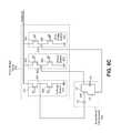
- FIG. 6Cillustrates the power bridge circuit 610 of FIG. 6A coupled to bi-directional coil assembly, under another embodiment.
- the bi-directional coil assembly 633includes capacitors C 3 and C 4 , and inductive coils L 4 and L 5 .
- the capacitor C 3 and the inductive coils L 4 and L 5are all coupled to a node 605 .
- the capacitor C 3is also coupled to the H-bridge branch 611 at the node 601 .
- the inductive coil L 4is further coupled to the shared branch 612 at the node 602 .
- the inductive coil L 5is coupled to both the node 605 and the node 603 on the sync bridge branch 613 .
- the capacitor C 4is coupled to both the shared branch 612 at the node 602 , and the sync bridge branch at the node 603 .
- the sync bridge branch 613In the power transmit mode, the sync bridge branch 613 is turned off and the current path through the bi-directional coil assembly 633 is the series combination of the capacitor C 3 and the inductive coil L 4 .
- the H-bridge branch 611In the power receive mode, the H-bridge branch 611 is turned off and the current path through the bi-directional coil assembly 633 is the series combination of inductive coils L 4 and L 5 in parallel with the capacitor C 4 .
- FIG. 6Dillustrates the power bridge circuit 610 of FIG. 6A coupled to yet another embodiment of the bi-directional coil assembly.
- the bi-directional coil assembly 634includes capacitors C 5 and C 6 , and inductive coils L 6 and L 7 .
- the capacitor C 5 and the inductive coil L 6are coupled to a node 606 .
- the capacitor C 5is also coupled to the H-bridge branch 611 at the node 601 .
- the inductive coil L 6is further coupled to the shared branch 612 at the node 602 .
- the capacitor C 6 and the inductive coil L 7are coupled in parallel and are coupled to both the shared bridge branch 612 at the node 602 and the sync bridge branch 613 at the node 603 .
- the sync bridge branch 613In the power transmit mode, the sync bridge branch 613 is turned off and the current path through the bi-directional coil assembly 634 is the series combination of the capacitor C 5 and the inductive coil L 6 .
- the H-bridge branch 611In the power receive mode, the H-bridge branch 611 is turned off and the current path through the bi-directional coil assembly 634 is parallel combination of the inductive coil L 7 and the capacitor C 6 .
- FIG. 7Aillustrates an embodiment of a bi-directional coil assembly.
- a bi-directional coil assembly 710includes an inductive coil 711 , and a capacitor 712 .
- the inductive coilis coupled to a node 713 and a node 715 .
- the inductive coil 711has a tap coupled to the capacitor 712 .
- the capacitoris also coupled to a node 714 as illustrated.
- the nodes 713 - 715are coupled to the power circuit bridge 610 of FIGS. 6A and 6B . According to an embodiment and referring back to FIG.
- the node 713is coupled to the shared branch 612 at node 602
- the node 714is coupled to the H-bridge branch 611 at node 601
- the node 715is coupled to the sync bridge branch 613 at node 613 .
- the bi-directional coil assembly 710includes two separate inductive coils coupled together instead of having an inductive coil 711 with a tap.
- FIG. 7Billustrates a current path 716 within the inductive coil assembly during the power receive mode of the inductive signal interface.
- the H-bridge branch 611is disabled during the power receive mode of the inductive signal interface. Accordingly, the power bridge circuit 610 provides the current path 716 between node 715 and 713 during the power receive mode.
- the current path 716includes the inductive coil 711 .
- FIG. 7Cillustrates a current path 717 within the inductive coil assembly during the power transmit mode of the inductive signal interface.
- the sync bridge branch 613 of FIG. 6Ais disabled during the power transmit mode of the inductive signal interface.
- the power bridge circuit 610provides the current path 717 between node 715 and 713 during the power transmit mode.
- the current path 717includes at least a portion of the inductive coil 711 and the capacitor 712 in series.
- FIG. 7Dillustrates another embodiment of the bi-directional coil assembly.
- a bi-directional coil assembly 720includes an inductive coil 721 , and capacitors 722 ( 1 ) and 722 ( 2 ).
- the inductive coilis coupled to a node 725 and the capacitor 722 ( 1 ).
- the capacitor 722 ( 1 )is also coupled to a node 724 as illustrated.
- the inductive coil 721has a tap coupled to a node 723 .
- the capacitor 722 ( 2 )is coupled to the nodes 725 and 723 .
- the nodes 723 - 725are coupled to the power circuit bridge 610 of FIGS. 6A and 6B . According to an embodiment and referring back to FIG.
- the node 723is coupled to the shared branch 612 at node 602
- the node 724is coupled to the H-bridge branch 611 at node 601
- the node 725is coupled to the sync bridge branch 613 at node 603 .
- the bi-directional coil assembly 720includes two inductive coils coupled together instead of having an inductive coil 721 with a tap.
- FIG. 7Eillustrates a current path 726 within the inductive coil assembly 720 during the power receive mode of the inductive signal interface.
- the H-bridge branch 611is disabled during the power receive mode of the inductive signal interface.
- the power bridge circuit 610provides the current path 726 between node 725 and 723 during the power receive mode which includes the parallel combination of at least a portion of the inductive coil 721 and the capacitor 722 ( 2 ).
- FIG. 7Fillustrates a current path 727 within the inductive coil assembly 720 during the power transmit mode of the inductive signal interface.
- the sync bridge branch 613 of FIG. 6Ais disabled during the power transmit mode of the inductive signal interface.
- the power bridge circuit 610provides the current path 727 between node 725 and 723 during the power transmit mode.
- the current path 727includes a series combination of at least a portion of the inductive coil 721 and the capacitor 722 ( 1 )
- the bi-directional coil assemblies 631 , 632 of FIGS. 6A and 6Bmay be alternatively configured according to any of the coil assembly topologies described above. Other variations are similarly possible.
- FIG. 8Aillustrates an operation of the power bridge circuit 610 of FIGS. 6A-6D in the power transmit mode.
- the power bridge circuit 610is configured to operate to deliver a current from the power I/O to a bi-directional coil assembly 810 , which may be any previously discussed coil assembly topology.
- the sync bridge branch 613is disabled, and the H-bridge branch 611 and the shared branch 612 are operable to deliver current from the signal line Power I/O, to the bi-directional coil assembly 810 , and finally to ground voltage along a current path 801 .
- FIG. 8Billustrates another operation of the power bridge circuit 610 of FIGS. 6A-6D in the power transmit mode.
- the H-bridge branch 611 and the shared branch 612are operable to deliver current from the signal line Power I/O, to the bi-directional coil assembly 810 , and finally to ground voltage along a current path 802 .
- the power bridge circuit 610 of FIG. 6Ais configurable to deliver a current to the bi-directional coil assembly 810 in a first direction (corresponding to the current path 801 ) and a reverse direction (corresponding to the current path 802 ).
- the power bridge circuit 610is operable to convert a received DC power signal to a high frequency power signal and to deliver the high frequency power signal to the bi-directional coil assembly 810 .
- FIG. 8Cillustrates an operation of the power bridge circuit 610 of FIGS. 6A-6D in the power receive mode.
- the power bridge circuit 610is configured to operate to deliver a current from the bi-directional coil assembly 810 to the signal line Power I/O.
- the H-bridge branch 611is disabled, and the sync bridge branch 613 and the shared branch 612 are operable to deliver current from ground voltage to the bi-directional coil assembly 810 , and finally to the signal line Power I/O along a current path 803 .
- FIG. 8Dillustrates another operation of the power bridge circuit 610 of FIGS. 6A-6D in the power receive mode.
- the sync bridge branch 613 and the shared branch 612are operable to deliver current from ground voltage to the bi-directional coil assembly 810 , and finally to the signal line Power I/O along a current path 804 .
- the power bridge circuit 610in the power receive mode, is configurable to carry a current from the bi-directional coil assembly 810 in a first direction (corresponding to the current path 803 ) and a reverse direction (corresponding to the current path 804 ). According to some embodiments, by carrying current in the first and the reverse directions from the bi-directional coil assembly 810 to the signal line Power I/O, the power bridge circuit 610 is operable to convert a high frequency power signal to a DC power signal and to deliver the DC power signal to the signal line Power I/O.
- Embodimentsrecognize that in at least some configurations, potential exist for one of the creation of a ‘flying node’—a node that acquires, at least in momentary instances, a voltage that is significantly higher than the voltage of its surrounding nodes.
- FIG. 8Edepicts a configuration that handles the occurrence of a flying node 698 , arising as a result of switching behavior at surrounding switches. Flying node 698 negatively affects the sync bridge branch 613 , as the H-bridge branch 611 and shared branch 612 are protected by either an inductor or capacitor. The flying node 698 is most problematic when relatively low tolerant FETs are used on at least the sync bridge branch 613 .
- An embodiment as depictedincorporates high voltage isolation devices 696 , which protect the sync bridge branch 613 when FETs are used for the respective gates. More specifically, the high voltage isolation devices 696 prevent low tolerance FETs from operating at voltages that exceed their respective operating voltage levels as a result of high voltages generated at the flying node 698 . Moreover, as the FETs typically incorporate diodes, unwanted diodic behavior resulting from high voltages is also avoided.
- the high voltage isolation devices 696can be implemented in various forms, including through use of FETs or other switches that allow the high voltage isolation devices 696 to be protected from high voltages stemming from flying node 698 .
- FIG. 9illustrates the combination two similarly structured computing devices, each using a “3-legged” power bridge circuit in accordance with any of the embodiments described herein.
- devices of different typese.g. mobile computing devices and docking stations
- the inductive use of a devicee.g. enable mobile computing device to both receive and transmit power inductively.
- two devicesare inductively linked that each include a power bridge circuit and a bi-directional coil assembly in accordance with embodiments described herein.
- the first inductive signal interface 920 ( 1 )transmits power through the inductive link 901 .
- a portion of the bi-directional coil assembly 911 on the first inductive signal interface 920 ( 1 )forms the inductive link 901 with a portion of the bi-directional coil assembly 912 on the second inductive signal interface 920 ( 2 ) to transfer power.
- the same circuit structuremay be used in both an inductive power transmitter (i.e. inductive signal interface 920 ( 1 )) and an inductive power receiver (i.e. inductive signal interface 920 ( 2 )).
- FIG. 10illustrates a power bridge circuit and a bi-directional coil assembly, together 1010 , coupled to current conditioning circuitry, under an embodiment.
- the power bridge circuit and bi-directional coil assembly combination 1010which may be any of the above described embodiments, is coupled via a signal line Power I/O to a decoupling circuit 1020 .
- the decoupling circuit 1020operates to act as a filter for certain signal frequencies and prevents those signals from passing through.
- the decoupling circuit 1020is coupled to a resistor 1024 .
- Probe nodes I sense 1 and I sense2 /V senseare coupled to the resistor 1024 as illustrated.
- the probe nodes I sense 1 and I sense2 /V senseare used to measure the current and voltage of the signal carried by the resistor 1024 .
- the measured current and voltagemay be used to adjust the operation of the power bridge circuit and bi-directional coil assembly combination 1010 .
- a switch 1021is coupled to the resistor 1024 at the node I sense2 /V sense and is controlled by a signal Input Pwr En. The switch 1021 operates to couple a power signal line Power In to the resistor 1024 in order to deliver power to the power bridge circuit and bi-directional coil assembly combination 1010 .
- Two transistors 1022 and 1023are coupled as illustrated to act as a voltage and current regulator for outgoing current from the power bridge circuit and bi-directional coil assembly combination 1010 .
- the transistors 1022 and 1023are controlled by signals Sync Buck FET 1 and Sync Buck FET 2 , respectively.
- FIG. 11is a representative diagram illustrating two computing devices that can be brought into contact for purpose of enabling one device to provide a power and/or data signal to the other device, according to an embodiment.
- Numerous embodiments described hereinmay be implemented using a mobile computing device and dock as two devices that are brought into contact with one another for purpose of power/data transfer without use of traditional insertive or mechanically coupled connectors.
- different kinds of devicese.g. portable devices and accessory devices
- two devices that are inductively coupledcorrespond to a mobile computing device (also referred to as an “MCD”) and an accessory device (specifically a dock or docking station).
- MCDmobile computing device
- an accessory devicespecifically a dock or docking station
- embodimentsmay also be implemented using other types of devices.
- the MCDis a mufti-purpose device having cellular data and telephonic capabilities
- the accessory devicecorresponds to, for example, a docking station (for communications and power supply), sticky (or piggy)-back accessory, a light projector, a speaker set, or headset station.
- the MCDmay include, for example, functionality for use as a media player, a camera or video recorder, a global positioning unit, an ultramobile personal computer, a laptop computer, or a multi-purpose computing device. Numerous other examples and implementations are described herein, including embodiments in which three or more devices are interconnected through one or more connector-less connections.
- a system 1100includes a MCD 1110 that is supported or otherwise retained by a dock 1120 .
- the manner in which the MCD 1110 is supportedmay vary.
- the orientation of the MCD on the dockmay be changed by the user for purpose of configuring operations or behavior of one or both devices.
- the MCD 1110is supported on the dock 1120 in a partially upright position along its length axis (L).
- Such an orientationmay correspond to a ‘portrait’ position.
- one or more ‘landscape’ positions, or positions in between the portrait and landscape positionsmay be possible.
- the dock 1120utilizes physical support structures (not shown), such as shelves, platforms, hooks or mechanical retention features, to retain the MCD 1110 in a docked or mated position.
- physical support structuressuch as shelves, platforms, hooks or mechanical retention features
- magnetic claspsmay be included or provided the dock 1120 and/or the MCD 1110 to secure retention of the MCD against the dock.
- the dock 1120may include resources 1121 for generating or extending power and/or data signals to the MCD 1110 .
- the dock 1120may be mated with a power outlet 1124 or another computer 1126 (e.g. desktop computer) to extend power and/or data signals.
- the resources 1121may include circuitry or hardware, such as AC/DC converters and regulators.
- the dock 1120may include a physical connector port, such as provided by a Universal Serial Bus (USB) connector.
- USBUniversal Serial Bus
- the dock 1120may include data acquisition capabilities, provided through connector ports with the computer 1126 , wireless ports (e.g. cellular, WiMax connection, Bluetooth), Internet ports, and media feeds (e.g. provided through television tuner and cable).
- the MCD 1110has a housing shell 1112 having a thickness (t).
- the housing shell 1112may be used to retain internal components of the MCD 1110 , such as a circuit board, processor, memory, or components of a display assembly.
- the MCD 1110may be structured so that a primary facade 1115 (e.g. the back panel) of the housing shell 1112 rests on a receiving surface 1125 of the dock 1120 .
- the two computing devicesare each provided an inductive signal interface 1119 , 1129 for enabling one device to inductively transmit power to the other device.
- the inductive signal interface 1119 , 1129 of each devicemay be implemented using a “three-legged” power bridge circuit such as described with FIG. 6A through 6D and elsewhere in this application. In this manner, embodiments described herein provide a system and technique for delivering electrical power from over short distances without the use of electrical conductors
- FIG. 11depicts two computing devices that use the “three-legged” power bridge circuit to inductively couple and signal power
- the two inductively paired devicesmay correspond to a mobile computing device and headset, two mobile computing devices, or mobile computing device and power-resourced holster.
Landscapes
- Engineering & Computer Science (AREA)
- Computer Networks & Wireless Communication (AREA)
- Power Engineering (AREA)
- Near-Field Transmission Systems (AREA)
Abstract
Description
Claims (20)
Priority Applications (5)
| Application Number | Priority Date | Filing Date | Title |
|---|---|---|---|
| US12/628,401US8954001B2 (en) | 2009-07-21 | 2009-12-01 | Power bridge circuit for bi-directional wireless power transmission |
| US12/841,001US8437695B2 (en) | 2009-07-21 | 2010-07-21 | Power bridge circuit for bi-directional inductive signaling |
| PCT/US2010/042779WO2011011536A2 (en) | 2009-07-21 | 2010-07-21 | Power bridge circuit for bi-directional inductive signaling |
| EP10802866.3AEP2457306B1 (en) | 2009-07-21 | 2010-07-21 | Power bridge circuit for bi-directional inductive power and data signal transfer |
| CN201080033338.7ACN102640393B (en) | 2009-07-21 | 2010-07-21 | Power Bridge Circuit for Bidirectional Inductive Signal Transmission |
Applications Claiming Priority (2)
| Application Number | Priority Date | Filing Date | Title |
|---|---|---|---|
| US22742309P | 2009-07-21 | 2009-07-21 | |
| US12/628,401US8954001B2 (en) | 2009-07-21 | 2009-12-01 | Power bridge circuit for bi-directional wireless power transmission |
Related Child Applications (1)
| Application Number | Title | Priority Date | Filing Date |
|---|---|---|---|
| US12/841,001Continuation-In-PartUS8437695B2 (en) | 2009-07-21 | 2010-07-21 | Power bridge circuit for bi-directional inductive signaling |
Publications (2)
| Publication Number | Publication Date |
|---|---|
| US20110018356A1 US20110018356A1 (en) | 2011-01-27 |
| US8954001B2true US8954001B2 (en) | 2015-02-10 |
Family
ID=43496643
Family Applications (1)
| Application Number | Title | Priority Date | Filing Date |
|---|---|---|---|
| US12/628,401Active2033-10-03US8954001B2 (en) | 2009-07-21 | 2009-12-01 | Power bridge circuit for bi-directional wireless power transmission |
Country Status (1)
| Country | Link |
|---|---|
| US (1) | US8954001B2 (en) |
Cited By (6)
| Publication number | Priority date | Publication date | Assignee | Title |
|---|---|---|---|---|
| US20130308256A1 (en)* | 2011-03-09 | 2013-11-21 | Hewlett-Packard Development Company, L.P. | Flat power coil for wireless charging applications |
| US20140312686A1 (en)* | 2011-06-21 | 2014-10-23 | Powermat Technologies Ltd. | In vehicle inductive power provision system and method |
| US20150207358A1 (en)* | 2014-01-17 | 2015-07-23 | Jung-Tsung Lin | Wireless charging moldule for a storage battery |
| US20160087474A1 (en)* | 2014-08-26 | 2016-03-24 | Christian Kellen Tallada | Apparatus, System and Method for Charging a Mobile Device |
| US20180034327A1 (en)* | 2015-03-06 | 2018-02-01 | Powerbyproxi Limited | Wireless power transfer adaptor |
| KR20230170880A (en) | 2020-02-26 | 2023-12-19 | 애플 인크. | Wireless power system |
Families Citing this family (18)
| Publication number | Priority date | Publication date | Assignee | Title |
|---|---|---|---|---|
| US8249308B2 (en)* | 2008-09-26 | 2012-08-21 | Robert Lussier | Portable intelligent fluorescence and transmittance imaging spectroscopy system |
| US8850045B2 (en) | 2008-09-26 | 2014-09-30 | Qualcomm Incorporated | System and method for linking and sharing resources amongst devices |
| US8395547B2 (en) | 2009-08-27 | 2013-03-12 | Hewlett-Packard Development Company, L.P. | Location tracking for mobile computing device |
| US8755815B2 (en) | 2010-08-31 | 2014-06-17 | Qualcomm Incorporated | Use of wireless access point ID for position determination |
| CN103222319B (en) | 2010-09-29 | 2016-08-10 | 高通股份有限公司 | A kind of method for mobile computing device and mobile computing device |
| US8760009B2 (en)* | 2011-05-25 | 2014-06-24 | Samuel Gong | Wireless power source |
| JP5899994B2 (en)* | 2012-02-10 | 2016-04-06 | ソニー株式会社 | Power feeding device, power receiving device, and program |
| US10756558B2 (en)* | 2012-03-29 | 2020-08-25 | Integrated Device Technology, Inc. | Establishing trusted relationships for multimodal wireless power transfer |
| CN103365388B (en)* | 2012-04-09 | 2017-02-22 | 华为终端有限公司 | Power supply method of terminal device and terminal device |
| KR101844409B1 (en) | 2012-10-23 | 2018-04-03 | 삼성전자주식회사 | Wireless energy transmission apparatus and method thereof, wireless energy transmission system |
| JP6249673B2 (en)* | 2013-08-13 | 2017-12-20 | ローム株式会社 | Contactless power supply system and receiver |
| US9872723B2 (en)* | 2013-09-24 | 2018-01-23 | Covidien Lp | Surgical instruments, systems, and methods incorporating wireless bi-directional communication |
| US10567865B2 (en)* | 2013-10-16 | 2020-02-18 | Voyetra Turtle Beach, Inc. | Electronic headset accessory |
| TWI632757B (en)* | 2015-09-30 | 2018-08-11 | 美商蘋果公司 | Apparatus for magnetic charging and optical data transfer |
| CN108539867A (en)* | 2017-03-02 | 2018-09-14 | 佑骅科技(深圳)有限公司 | The wireless power transmitting device of transceiver |
| WO2018190985A1 (en)* | 2017-04-14 | 2018-10-18 | General Electric Company | A wireless power transceiver device and an associated method thereof |
| US10396779B2 (en)* | 2017-05-31 | 2019-08-27 | Texas Instruments Incorporated | Ground switching for speaker current sense |
| US11176560B2 (en)* | 2019-08-02 | 2021-11-16 | Capital One Services, Llc | Systems, methods and devices for ATM access during outages |
Citations (131)
| Publication number | Priority date | Publication date | Assignee | Title |
|---|---|---|---|---|
| FR2601161A1 (en) | 1986-07-02 | 1988-01-08 | Crouzet Sa | Information processing device |
| EP0395469A2 (en) | 1989-04-14 | 1990-10-31 | Telematique Videotex Francaise T.V.F. | Portable microcomputer |
| US5375226A (en) | 1988-12-29 | 1994-12-20 | Toppan Moore Company, Ltd. | Portable type data entry terminal having a keyboard input device and a graphic input device |
| WO1995003686A1 (en) | 1993-07-23 | 1995-02-02 | Steven James Shattil | Active electromagnetic shielding |
| US5455466A (en) | 1993-07-29 | 1995-10-03 | Dell Usa, L.P. | Inductive coupling system for power and data transfer |
| US5596567A (en) | 1995-03-31 | 1997-01-21 | Motorola, Inc. | Wireless battery charging system |
| US5600225A (en) | 1994-06-30 | 1997-02-04 | Nippon Electric Co | Noncontacting charging device |
| US5666530A (en) | 1992-12-02 | 1997-09-09 | Compaq Computer Corporation | System for automatic synchronization of common file between portable computer and host computer via communication channel selected from a plurality of usable channels there between |
| JPH09259241A (en) | 1996-03-27 | 1997-10-03 | Matsushita Electric Works Ltd | Transmission head for electromagnetically coupled id device |
| US5733313A (en) | 1996-08-01 | 1998-03-31 | Exonix Corporation | RF coupled, implantable medical device with rechargeable back-up power source |
| US5760580A (en) | 1994-04-26 | 1998-06-02 | Rso Corporation N.V. | Method for excitation and detection of magnetic elements by a mechanical resonance |
| US5831348A (en) | 1996-06-03 | 1998-11-03 | Mitsubishi Denki Kabushiki Kaisha | Secondary circuit device for wireless transmit-receive system and induction coil for wireless transmit-receive system |
| US5958051A (en) | 1996-11-27 | 1999-09-28 | Sun Microsystems, Inc. | Implementing digital signatures for data streams and data archives |
| US6006274A (en) | 1997-01-30 | 1999-12-21 | 3Com Corporation | Method and apparatus using a pass through personal computer connected to both a local communication link and a computer network for indentifying and synchronizing a preferred computer with a portable computer |
| JPH11354348A (en) | 1998-06-04 | 1999-12-24 | Furukawa Electric Co Ltd:The | Separation transformer |
| US6138245A (en) | 1999-02-05 | 2000-10-24 | Neopoint, Inc. | System and method for automatic device synchronization |
| US6184651B1 (en) | 2000-03-20 | 2001-02-06 | Motorola, Inc. | Contactless battery charger with wireless control link |
| JP3161388B2 (en) | 1997-11-05 | 2001-04-25 | 日本電気株式会社 | Docking bay system |
| US6266539B1 (en) | 1998-06-12 | 2001-07-24 | Cisco Technology, Inc. | Telephone docking station for personal digital assistant |
| US6330436B1 (en) | 1999-04-30 | 2001-12-11 | Lucent Technologies, Inc. | Enhanced wireless messaging notification system |
| US6389423B1 (en) | 1999-04-13 | 2002-05-14 | Mitsubishi Denki Kabushiki Kaisha | Data synchronization method for maintaining and controlling a replicated data |
| US6400274B1 (en) | 1995-08-31 | 2002-06-04 | Intermec Ip Corp. | High-performance mobile power antennas |
| US6405049B2 (en) | 1997-08-05 | 2002-06-11 | Symbol Technologies, Inc. | Portable data terminal and cradle |
| US20020084698A1 (en) | 2000-11-20 | 2002-07-04 | Kelly Clifford Mark | Electrically isolated power and signal coupler system for a patient connected device |
| US20020103008A1 (en) | 2001-01-29 | 2002-08-01 | Rahn Michael D. | Cordless communication between PDA and host computer using cradle |
| US6436299B1 (en) | 1999-06-21 | 2002-08-20 | Amway Corporation | Water treatment system with an inductively coupled ballast |
| US6445936B1 (en) | 1999-11-16 | 2002-09-03 | Agere Systems Guardian Corp. | Low power consumption quick charge for wireless device |
| US6501364B1 (en) | 2001-06-15 | 2002-12-31 | City University Of Hong Kong | Planar printed-circuit-board transformers with effective electromagnetic interference (EMI) shielding |
| US6510424B1 (en) | 1999-10-22 | 2003-01-21 | International Business Machines Corporation | Electronic notification agent |
| US6515878B1 (en) | 1997-08-08 | 2003-02-04 | Meins Juergen G. | Method and apparatus for supplying contactless power |
| US6532152B1 (en) | 1998-11-16 | 2003-03-11 | Intermec Ip Corp. | Ruggedized hand held computer |
| US20030214255A1 (en) | 1999-06-21 | 2003-11-20 | Baarman David W. | Inductively powered apparatus |
| US20030233455A1 (en) | 2002-06-14 | 2003-12-18 | Mike Leber | Distributed file sharing system |
| US6673250B2 (en) | 1999-06-21 | 2004-01-06 | Access Business Group International Llc | Radio frequency identification system for a fluid treatment system |
| US6731071B2 (en) | 1999-06-21 | 2004-05-04 | Access Business Group International Llc | Inductively powered lamp assembly |
| US20040088012A1 (en) | 2002-10-30 | 2004-05-06 | Kroll Mark W. | Implantable stimulation device with isolating system for minimizing magnetic induction |
| US20040130916A1 (en) | 1999-06-21 | 2004-07-08 | Baarman David W. | Adaptive inductive power supply |
| US20040130915A1 (en) | 1999-06-21 | 2004-07-08 | Baarman David W. | Adaptive inductive power supply with communication |
| US20040150934A1 (en) | 2003-02-04 | 2004-08-05 | Baarman David W. | Adapter |
| US6795110B1 (en) | 1999-06-15 | 2004-09-21 | Philip Kossin | Weatherproof and watertight digital electronic camera, including a solid or fluid-filled digital camera operating at great depths |
| US6803744B1 (en) | 1999-11-01 | 2004-10-12 | Anthony Sabo | Alignment independent and self aligning inductive power transfer system |
| US6806649B2 (en) | 2002-02-19 | 2004-10-19 | Access Business Group International Llc | Starter assembly for a gas discharge lamp |
| US6810405B1 (en) | 1998-08-18 | 2004-10-26 | Starfish Software, Inc. | System and methods for synchronizing data between multiple datasets |
| WO2004098079A1 (en) | 2003-04-25 | 2004-11-11 | Apple Computer Inc. | Media player system |
| US6825620B2 (en) | 1999-06-21 | 2004-11-30 | Access Business Group International Llc | Inductively coupled ballast circuit |
| US20040259499A1 (en) | 2001-07-18 | 2004-12-23 | Haruo Oba | Communication system and method |
| US20040266362A1 (en) | 2003-06-27 | 2004-12-30 | Watkins Ronald Dean | Transmit/receive switch |
| US20050007067A1 (en) | 1999-06-21 | 2005-01-13 | Baarman David W. | Vehicle interface |
| CN1592197A (en) | 2003-09-01 | 2005-03-09 | 台均实业有限公司 | Method for authentication between client device and local client application or remote network service |
| WO2005024865A2 (en) | 2003-09-08 | 2005-03-17 | Splashpower Limited | Inductive power transfer units having flux shields |
| US6888438B2 (en) | 2001-06-15 | 2005-05-03 | City University Of Hong Kong | Planar printed circuit-board transformers with effective electromagnetic interference (EMI) shielding |
| GB2389720B (en) | 2002-06-10 | 2005-09-07 | Univ City Hong Kong | Planar inductive battery charger |
| GB2399466B (en) | 2003-03-10 | 2005-11-16 | Univ City Hong Kong | Battery charging system |
| US6975198B2 (en) | 2003-02-04 | 2005-12-13 | Access Business Group International Llc | Inductive coil assembly |
| US6986051B2 (en) | 2000-04-13 | 2006-01-10 | International Business Machines Corporation | Method and system for controlling and filtering files using a virus-free certificate |
| US20060041420A1 (en) | 2004-06-30 | 2006-02-23 | Threshold Corporation | Method and apparatus for configuring a network appliance |
| US20060061958A1 (en) | 2004-09-17 | 2006-03-23 | Mark Solomon | Portable computer docking station |
| GB2389767B (en) | 2002-06-10 | 2006-04-19 | Univ City Hong Kong | Apparatus for energy transfer by induction |
| US20060123055A1 (en) | 2004-12-07 | 2006-06-08 | Paul Atkinson | Device and method for selectively controlling the utility of a target |
| US7065658B1 (en) | 2001-05-18 | 2006-06-20 | Palm, Incorporated | Method and apparatus for synchronizing and recharging a connector-less portable computer system |
| US20060132045A1 (en) | 2004-12-17 | 2006-06-22 | Baarman David W | Heating system and heater |
| US20060187049A1 (en) | 2005-02-09 | 2006-08-24 | Atmel Germany Gmbh | Circuit arrangement and method for supplying power to a transponder |
| US7149473B1 (en) | 1999-01-15 | 2006-12-12 | Nokia Corporation | Interface |
| US7164255B2 (en) | 2002-06-10 | 2007-01-16 | City University Of Hong Kong | Inductive battery charger system with primary transformer windings formed in a multi-layer structure |
| US20070035917A1 (en) | 2005-08-09 | 2007-02-15 | Apple Computer, Inc. | Methods and apparatuses for docking a portable electronic device that has a planar like configuration and that operates in multiple orientations |
| WO2007034421A2 (en) | 2005-09-23 | 2007-03-29 | Ipico Innovation Inc. | Radio frequency identification device systems |
| US20070120752A1 (en) | 2005-11-30 | 2007-05-31 | Nobuaki Takasu | Information processing apparatus, information processing system and radio communication control method |
| US7248017B2 (en) | 2002-05-13 | 2007-07-24 | Spashpower Limited | Portable contact-less power transfer devices and rechargeable batteries |
| US20070182367A1 (en) | 2006-01-31 | 2007-08-09 | Afshin Partovi | Inductive power source and charging system |
| US20070188284A1 (en) | 2003-02-26 | 2007-08-16 | Dobbs John M | Shielded power coupling device |
| US7262700B2 (en) | 2005-03-10 | 2007-08-28 | Microsoft Corporation | Inductive powering surface for powering portable devices |
| US7271569B2 (en) | 2004-09-21 | 2007-09-18 | Motorola Inc. | Contact less charger with alignment indicator |
| US7286880B2 (en) | 2003-10-02 | 2007-10-23 | Medtronic, Inc. | System and method for transcutaneous energy transfer achieving high efficiency |
| US20070246546A1 (en) | 2006-04-20 | 2007-10-25 | Yuko Yoshida | Information Processing Terminal, IC Card, Portable Communication Device, Wireless Communication Method, and Program |
| WO2007141078A1 (en) | 2006-06-02 | 2007-12-13 | SIEMENS AKTIENGESELLSCHAFT öSTERREICH | Inverter circuit and method for operating the inverter circuit |
| US20070290654A1 (en) | 2006-06-14 | 2007-12-20 | Assaf Govari | Inductive charging of tools on surgical tray |
| US7323964B1 (en)* | 2006-11-23 | 2008-01-29 | National Central University | Non-contact power system with load and gap detection |
| US7331793B2 (en) | 2005-12-16 | 2008-02-19 | Motorola, Inc. | Magnetic connector |
| WO2008033670A2 (en) | 2006-09-11 | 2008-03-20 | Apple Inc. | Highly portable media devices |
| WO2008044875A1 (en) | 2006-10-10 | 2008-04-17 | Ls Cable, Ltd. | Rechargeable power supply, battery device, contact-less charger systems and method for charging rechargeable battery cell |
| US7375492B2 (en) | 2003-12-12 | 2008-05-20 | Microsoft Corporation | Inductively charged battery pack |
| US7382636B2 (en) | 2005-10-14 | 2008-06-03 | Access Business Group International Llc | System and method for powering a load |
| US20080133918A1 (en) | 2006-12-04 | 2008-06-05 | Samsung Electronics Co., Ltd. | Method and apparatus for transmitting data using authentication |
| KR100836634B1 (en) | 2006-10-24 | 2008-06-10 | 주식회사 한림포스텍 | Portable terminal using a contactless charger, a battery pack for charging and a contactless charger for wireless data communication and power transmission |
| US7385357B2 (en) | 1999-06-21 | 2008-06-10 | Access Business Group International Llc | Inductively coupled ballast circuit |
| US7392059B2 (en) | 2001-05-14 | 2008-06-24 | Innovision Research & Technology Plc | Electrical devices |
| US20080196086A1 (en) | 2007-02-09 | 2008-08-14 | Sony Corporation, A Japanese Corporation | Method and apparatus for authorizing a communication interface |
| US7414380B2 (en) | 2004-09-21 | 2008-08-19 | Lear Corporation | Apparatus for inductively recharging batteries of a portable convenience device |
| US20080231537A1 (en) | 2007-03-19 | 2008-09-25 | Ahmadreza Rofougaran | Method and system for fm transmit and fm receive using a transformer as a duplexer |
| US7446672B2 (en) | 2005-03-24 | 2008-11-04 | M&Fc Holding, Llc | Method and apparatus for coupling a meter register to an automatic meter reading communication device |
| WO2008133806A1 (en) | 2007-04-23 | 2008-11-06 | Eastman Kodak Company | Charging display system |
| US20080278894A1 (en) | 2007-05-11 | 2008-11-13 | Miradia Inc. | Docking station for projection display applications |
| US7454170B2 (en) | 2003-08-08 | 2008-11-18 | Koninklijke Philips Electronics N.V. | Unidirectional power and bi-directional data transfer over a single inductive coupling |
| US7462951B1 (en) | 2004-08-11 | 2008-12-09 | Access Business Group International Llc | Portable inductive power station |
| US7471986B2 (en) | 2004-02-20 | 2008-12-30 | Cardiac Pacemakers, Inc. | System and method for transmitting energy to and establishing a communications network with one or more implanted devices |
| US20090001932A1 (en) | 2007-06-29 | 2009-01-01 | Seiko Epson Corporation | Power transmission control device, power transmission device, non-contact power transmission system, and electronic instrument |
| US20090001941A1 (en) | 2007-06-29 | 2009-01-01 | Microsoft Corporation | Inductive Powering Surface for Powering Portable Devices |
| US20090008148A1 (en) | 2007-07-03 | 2009-01-08 | Shinko Electric Industries Co., Ltd. | Inductor built-in wiring board having shield function |
| US7495414B2 (en) | 2005-07-25 | 2009-02-24 | Convenient Power Limited | Rechargeable battery circuit and structure for compatibility with a planar inductive charging platform |
| US20090069869A1 (en) | 2007-09-11 | 2009-03-12 | Advanced Bionics Corporation | Rotating field inductive data telemetry and power transfer in an implantable medical device system |
| US20090088077A1 (en) | 2005-04-11 | 2009-04-02 | Innovision Research & Technology Plc | Communications Apparatus |
| US7521890B2 (en) | 2005-12-27 | 2009-04-21 | Power Science Inc. | System and method for selective transfer of radio frequency power |
| US20090106567A1 (en) | 2007-10-17 | 2009-04-23 | Access Business Group International Llc | Laptop and portable electronic device wireless power supply systems |
| WO2009057771A1 (en) | 2007-11-01 | 2009-05-07 | Meidensha Corporation | Electronic authentication device, electronic authentication system, electronic authentication method and its program |
| US20090170433A1 (en) | 2007-12-28 | 2009-07-02 | Mark Rhodes | Inductive communications system |
| US20090212737A1 (en) | 2008-02-25 | 2009-08-27 | L & P Property Management Company | Inductively coupled shelving and storage containers |
| US20090212637A1 (en) | 2008-02-22 | 2009-08-27 | Access Business Group International Llc | Magnetic positioning for inductive coupling |
| US20100007449A1 (en) | 2008-04-03 | 2010-01-14 | Tait Towers Inc. | Magnetically coupled device |
| WO2010005324A1 (en) | 2008-07-07 | 2010-01-14 | Powerbyproxi Limited | A contactless power receiver and method of operation |
| US20100021176A1 (en) | 2006-11-16 | 2010-01-28 | Integration Associates Inc. | Apparatus and Method for Near-Field Communication |
| US20100045269A1 (en) | 2001-03-16 | 2010-02-25 | Lafranchise Jeffrey R | Methods and apparatus to detect location and orientation in an inductive system |
| US20100070219A1 (en) | 2007-03-22 | 2010-03-18 | Powermat Ltd | Efficiency monitor for inductive power transmission |
| US20100076524A1 (en) | 2003-10-02 | 2010-03-25 | Medtronic, Inc. | Inductively rechargeable external energy source, charger, system and method for a transcutaneous inductive charger for an implantable medical device |
| US20100081483A1 (en) | 2008-09-26 | 2010-04-01 | Manjirnath Chatterjee | Shield for use with a computing device that receives an inductive signal transmission |
| US20100081473A1 (en) | 2008-09-26 | 2010-04-01 | Manjirnath Chatterjee | Orientation and presence detection for use in configuring operations of computing devices in docked environments |
| US20100081377A1 (en) | 2008-09-26 | 2010-04-01 | Manjirnath Chatterjee | Magnetic latching mechanism for use in mating a mobile computing device to an accessory device |
| US20100083012A1 (en) | 2008-09-26 | 2010-04-01 | Mark Corbridge | Inductive Signal Transfer System for Computing Devices |
| US20100121965A1 (en) | 2008-11-12 | 2010-05-13 | Palm, Inc. | Protocol for Program during Startup Sequence |
| US20100131691A1 (en) | 2008-09-26 | 2010-05-27 | Manjirnath Chatterjee | Extending device functionality amongst inductively linked devices |
| WO2010062198A1 (en) | 2008-11-26 | 2010-06-03 | Auckland Uniservices Limited | Bi-directional inductive power transfer |
| US20100146308A1 (en) | 2008-09-26 | 2010-06-10 | Richard Gioscia | Portable power supply device for mobile computing devices |
| US20100148723A1 (en) | 2008-09-02 | 2010-06-17 | Qualcomm Incorporated | Bidirectional wireless power transmission |
| WO2010068062A2 (en) | 2008-12-12 | 2010-06-17 | 주식회사 한림포스텍 | Contactless power transmission device |
| US7743151B2 (en) | 2004-08-05 | 2010-06-22 | Cardiac Pacemakers, Inc. | System and method for providing digital data communications over a wireless intra-body network |
| US20100156193A1 (en) | 2008-12-23 | 2010-06-24 | Mark Rhodes | Inductively coupled data and power transfer system and apparatus |
| US20100172090A1 (en) | 2009-01-05 | 2010-07-08 | Manjirnath Chatterjee | Interior connector scheme for accessorizing a mobile computing device with a removeable housing segment |
| US20100194336A1 (en) | 2007-10-18 | 2010-08-05 | Powermat Ltd. | Inductively chargeable audio devices |
| WO2010091269A1 (en) | 2009-02-06 | 2010-08-12 | Baylor College Of Medicine | Real-time magnetic dipole detection and tracking |
| US20110106954A1 (en) | 2008-09-26 | 2011-05-05 | Manjirnath Chatterjee | System and method for inductively pairing devices to share data or resources |
| US20120042087A1 (en) | 2008-09-26 | 2012-02-16 | Samantha Berg | System and method for linking and sharing resources amongst devices |
| US8278784B2 (en) | 2008-07-28 | 2012-10-02 | Qualcomm Incorporated | Wireless power transmission for electronic devices |
Family Cites Families (1)
| Publication number | Priority date | Publication date | Assignee | Title |
|---|---|---|---|---|
| JP2001079262A (en)* | 1999-09-10 | 2001-03-27 | Sony Computer Entertainment Inc | Information processing device, entertainment device, start image display method and information recording medium |
- 2009
- 2009-12-01USUS12/628,401patent/US8954001B2/enactiveActive
Patent Citations (157)
| Publication number | Priority date | Publication date | Assignee | Title |
|---|---|---|---|---|
| FR2601161A1 (en) | 1986-07-02 | 1988-01-08 | Crouzet Sa | Information processing device |
| US5375226A (en) | 1988-12-29 | 1994-12-20 | Toppan Moore Company, Ltd. | Portable type data entry terminal having a keyboard input device and a graphic input device |
| EP0395469A2 (en) | 1989-04-14 | 1990-10-31 | Telematique Videotex Francaise T.V.F. | Portable microcomputer |
| US5666530A (en) | 1992-12-02 | 1997-09-09 | Compaq Computer Corporation | System for automatic synchronization of common file between portable computer and host computer via communication channel selected from a plurality of usable channels there between |
| WO1995003686A1 (en) | 1993-07-23 | 1995-02-02 | Steven James Shattil | Active electromagnetic shielding |
| US5455466A (en) | 1993-07-29 | 1995-10-03 | Dell Usa, L.P. | Inductive coupling system for power and data transfer |
| US5760580A (en) | 1994-04-26 | 1998-06-02 | Rso Corporation N.V. | Method for excitation and detection of magnetic elements by a mechanical resonance |
| US5600225A (en) | 1994-06-30 | 1997-02-04 | Nippon Electric Co | Noncontacting charging device |
| US5596567A (en) | 1995-03-31 | 1997-01-21 | Motorola, Inc. | Wireless battery charging system |
| US6400274B1 (en) | 1995-08-31 | 2002-06-04 | Intermec Ip Corp. | High-performance mobile power antennas |
| JPH09259241A (en) | 1996-03-27 | 1997-10-03 | Matsushita Electric Works Ltd | Transmission head for electromagnetically coupled id device |
| US5831348A (en) | 1996-06-03 | 1998-11-03 | Mitsubishi Denki Kabushiki Kaisha | Secondary circuit device for wireless transmit-receive system and induction coil for wireless transmit-receive system |
| US5733313A (en) | 1996-08-01 | 1998-03-31 | Exonix Corporation | RF coupled, implantable medical device with rechargeable back-up power source |
| US5958051A (en) | 1996-11-27 | 1999-09-28 | Sun Microsystems, Inc. | Implementing digital signatures for data streams and data archives |
| US6006274A (en) | 1997-01-30 | 1999-12-21 | 3Com Corporation | Method and apparatus using a pass through personal computer connected to both a local communication link and a computer network for indentifying and synchronizing a preferred computer with a portable computer |
| US6405049B2 (en) | 1997-08-05 | 2002-06-11 | Symbol Technologies, Inc. | Portable data terminal and cradle |
| US6515878B1 (en) | 1997-08-08 | 2003-02-04 | Meins Juergen G. | Method and apparatus for supplying contactless power |
| JP3161388B2 (en) | 1997-11-05 | 2001-04-25 | 日本電気株式会社 | Docking bay system |
| JPH11354348A (en) | 1998-06-04 | 1999-12-24 | Furukawa Electric Co Ltd:The | Separation transformer |
| US6266539B1 (en) | 1998-06-12 | 2001-07-24 | Cisco Technology, Inc. | Telephone docking station for personal digital assistant |
| US6810405B1 (en) | 1998-08-18 | 2004-10-26 | Starfish Software, Inc. | System and methods for synchronizing data between multiple datasets |
| US6532152B1 (en) | 1998-11-16 | 2003-03-11 | Intermec Ip Corp. | Ruggedized hand held computer |
| US7149473B1 (en) | 1999-01-15 | 2006-12-12 | Nokia Corporation | Interface |
| US6138245A (en) | 1999-02-05 | 2000-10-24 | Neopoint, Inc. | System and method for automatic device synchronization |
| US6389423B1 (en) | 1999-04-13 | 2002-05-14 | Mitsubishi Denki Kabushiki Kaisha | Data synchronization method for maintaining and controlling a replicated data |
| US6330436B1 (en) | 1999-04-30 | 2001-12-11 | Lucent Technologies, Inc. | Enhanced wireless messaging notification system |
| US6795110B1 (en) | 1999-06-15 | 2004-09-21 | Philip Kossin | Weatherproof and watertight digital electronic camera, including a solid or fluid-filled digital camera operating at great depths |
| US6673250B2 (en) | 1999-06-21 | 2004-01-06 | Access Business Group International Llc | Radio frequency identification system for a fluid treatment system |
| US7126450B2 (en) | 1999-06-21 | 2006-10-24 | Access Business Group International Llc | Inductively powered apparatus |
| US20050127850A1 (en) | 1999-06-21 | 2005-06-16 | Baarman David W. | Inductively powered apparatus |
| US20050127849A1 (en) | 1999-06-21 | 2005-06-16 | Baarman David W. | Inductively powered apparatus |
| US20030214255A1 (en) | 1999-06-21 | 2003-11-20 | Baarman David W. | Inductively powered apparatus |
| US20050122059A1 (en) | 1999-06-21 | 2005-06-09 | Baarman David W. | Inductively powered apparatus |
| US20050122058A1 (en) | 1999-06-21 | 2005-06-09 | Baarman David W. | Inductively powered apparatus |
| US6731071B2 (en) | 1999-06-21 | 2004-05-04 | Access Business Group International Llc | Inductively powered lamp assembly |
| US20050116650A1 (en) | 1999-06-21 | 2005-06-02 | Baarman David W. | Method of manufacturing a lamp assembly |
| US20040130916A1 (en) | 1999-06-21 | 2004-07-08 | Baarman David W. | Adaptive inductive power supply |
| US20040130915A1 (en) | 1999-06-21 | 2004-07-08 | Baarman David W. | Adaptive inductive power supply with communication |
| US7385357B2 (en) | 1999-06-21 | 2008-06-10 | Access Business Group International Llc | Inductively coupled ballast circuit |
| US7118240B2 (en) | 1999-06-21 | 2006-10-10 | Access Business Group International Llc | Inductively powered apparatus |
| US6812645B2 (en) | 1999-06-21 | 2004-11-02 | Access Business Group International Llc | Inductively powered lamp assembly |
| US20050007067A1 (en) | 1999-06-21 | 2005-01-13 | Baarman David W. | Vehicle interface |
| US6436299B1 (en) | 1999-06-21 | 2002-08-20 | Amway Corporation | Water treatment system with an inductively coupled ballast |
| US6831417B2 (en) | 1999-06-21 | 2004-12-14 | Access Business Group International Llc | Method of manufacturing a lamp assembly |
| US6825620B2 (en) | 1999-06-21 | 2004-11-30 | Access Business Group International Llc | Inductively coupled ballast circuit |
| US20050093475A1 (en) | 1999-06-21 | 2005-05-05 | Kuennen Roy W. | Inductively coupled ballast circuit |
| US6510424B1 (en) | 1999-10-22 | 2003-01-21 | International Business Machines Corporation | Electronic notification agent |
| US6803744B1 (en) | 1999-11-01 | 2004-10-12 | Anthony Sabo | Alignment independent and self aligning inductive power transfer system |
| US6445936B1 (en) | 1999-11-16 | 2002-09-03 | Agere Systems Guardian Corp. | Low power consumption quick charge for wireless device |
| US6184651B1 (en) | 2000-03-20 | 2001-02-06 | Motorola, Inc. | Contactless battery charger with wireless control link |
| US6986051B2 (en) | 2000-04-13 | 2006-01-10 | International Business Machines Corporation | Method and system for controlling and filtering files using a virus-free certificate |
| US6917163B2 (en) | 2000-06-12 | 2005-07-12 | Access Business Group International Llc | Inductively powered lamp assembly |
| US20020084698A1 (en) | 2000-11-20 | 2002-07-04 | Kelly Clifford Mark | Electrically isolated power and signal coupler system for a patient connected device |
| US20020103008A1 (en) | 2001-01-29 | 2002-08-01 | Rahn Michael D. | Cordless communication between PDA and host computer using cradle |
| US20100045269A1 (en) | 2001-03-16 | 2010-02-25 | Lafranchise Jeffrey R | Methods and apparatus to detect location and orientation in an inductive system |
| US7392059B2 (en) | 2001-05-14 | 2008-06-24 | Innovision Research & Technology Plc | Electrical devices |
| US7065658B1 (en) | 2001-05-18 | 2006-06-20 | Palm, Incorporated | Method and apparatus for synchronizing and recharging a connector-less portable computer system |
| US6888438B2 (en) | 2001-06-15 | 2005-05-03 | City University Of Hong Kong | Planar printed circuit-board transformers with effective electromagnetic interference (EMI) shielding |
| US6501364B1 (en) | 2001-06-15 | 2002-12-31 | City University Of Hong Kong | Planar printed-circuit-board transformers with effective electromagnetic interference (EMI) shielding |
| US20040259499A1 (en) | 2001-07-18 | 2004-12-23 | Haruo Oba | Communication system and method |
| US6806649B2 (en) | 2002-02-19 | 2004-10-19 | Access Business Group International Llc | Starter assembly for a gas discharge lamp |
| US20040222751A1 (en) | 2002-02-19 | 2004-11-11 | Mollema Scott A. | Starter assembly for a gas discharge lamp |
| US7248017B2 (en) | 2002-05-13 | 2007-07-24 | Spashpower Limited | Portable contact-less power transfer devices and rechargeable batteries |
| US7164255B2 (en) | 2002-06-10 | 2007-01-16 | City University Of Hong Kong | Inductive battery charger system with primary transformer windings formed in a multi-layer structure |
| GB2389767B (en) | 2002-06-10 | 2006-04-19 | Univ City Hong Kong | Apparatus for energy transfer by induction |
| GB2389720B (en) | 2002-06-10 | 2005-09-07 | Univ City Hong Kong | Planar inductive battery charger |
| US7576514B2 (en) | 2002-06-10 | 2009-08-18 | Cityu Research Limited | Planar inductive battery charging system |
| US20030233455A1 (en) | 2002-06-14 | 2003-12-18 | Mike Leber | Distributed file sharing system |
| US20040088012A1 (en) | 2002-10-30 | 2004-05-06 | Kroll Mark W. | Implantable stimulation device with isolating system for minimizing magnetic induction |
| US7132918B2 (en) | 2003-02-04 | 2006-11-07 | Access Business Group International Llc | Inductive coil assembly |
| US20040150934A1 (en) | 2003-02-04 | 2004-08-05 | Baarman David W. | Adapter |
| US6975198B2 (en) | 2003-02-04 | 2005-12-13 | Access Business Group International Llc | Inductive coil assembly |
| US7518267B2 (en) | 2003-02-04 | 2009-04-14 | Access Business Group International Llc | Power adapter for a remote device |
| US7116200B2 (en) | 2003-02-04 | 2006-10-03 | Access Business Group International Llc | Inductive coil assembly |
| US20040232845A1 (en) | 2003-02-04 | 2004-11-25 | Baarman David W. | Inductive coil assembly |
| US20070188284A1 (en) | 2003-02-26 | 2007-08-16 | Dobbs John M | Shielded power coupling device |
| GB2399466B (en) | 2003-03-10 | 2005-11-16 | Univ City Hong Kong | Battery charging system |
| US7627343B2 (en)* | 2003-04-25 | 2009-12-01 | Apple Inc. | Media player system |
| WO2004098079A1 (en) | 2003-04-25 | 2004-11-11 | Apple Computer Inc. | Media player system |
| US20040266362A1 (en) | 2003-06-27 | 2004-12-30 | Watkins Ronald Dean | Transmit/receive switch |
| US7454170B2 (en) | 2003-08-08 | 2008-11-18 | Koninklijke Philips Electronics N.V. | Unidirectional power and bi-directional data transfer over a single inductive coupling |
| CN1592197A (en) | 2003-09-01 | 2005-03-09 | 台均实业有限公司 | Method for authentication between client device and local client application or remote network service |
| WO2005024865A2 (en) | 2003-09-08 | 2005-03-17 | Splashpower Limited | Inductive power transfer units having flux shields |
| US20070064406A1 (en) | 2003-09-08 | 2007-03-22 | Beart Pilgrim G W | Inductive power transfer units having flux shields |
| US7286880B2 (en) | 2003-10-02 | 2007-10-23 | Medtronic, Inc. | System and method for transcutaneous energy transfer achieving high efficiency |
| US20100076524A1 (en) | 2003-10-02 | 2010-03-25 | Medtronic, Inc. | Inductively rechargeable external energy source, charger, system and method for a transcutaneous inductive charger for an implantable medical device |
| US7375492B2 (en) | 2003-12-12 | 2008-05-20 | Microsoft Corporation | Inductively charged battery pack |
| US7471986B2 (en) | 2004-02-20 | 2008-12-30 | Cardiac Pacemakers, Inc. | System and method for transmitting energy to and establishing a communications network with one or more implanted devices |
| US20060041420A1 (en) | 2004-06-30 | 2006-02-23 | Threshold Corporation | Method and apparatus for configuring a network appliance |
| US7743151B2 (en) | 2004-08-05 | 2010-06-22 | Cardiac Pacemakers, Inc. | System and method for providing digital data communications over a wireless intra-body network |
| US7462951B1 (en) | 2004-08-11 | 2008-12-09 | Access Business Group International Llc | Portable inductive power station |
| US20060061958A1 (en) | 2004-09-17 | 2006-03-23 | Mark Solomon | Portable computer docking station |
| US7271569B2 (en) | 2004-09-21 | 2007-09-18 | Motorola Inc. | Contact less charger with alignment indicator |
| US7414380B2 (en) | 2004-09-21 | 2008-08-19 | Lear Corporation | Apparatus for inductively recharging batteries of a portable convenience device |
| US20060123055A1 (en) | 2004-12-07 | 2006-06-08 | Paul Atkinson | Device and method for selectively controlling the utility of a target |
| US20060132045A1 (en) | 2004-12-17 | 2006-06-22 | Baarman David W | Heating system and heater |
| US20060187049A1 (en) | 2005-02-09 | 2006-08-24 | Atmel Germany Gmbh | Circuit arrangement and method for supplying power to a transponder |
| US7262700B2 (en) | 2005-03-10 | 2007-08-28 | Microsoft Corporation | Inductive powering surface for powering portable devices |
| US7446672B2 (en) | 2005-03-24 | 2008-11-04 | M&Fc Holding, Llc | Method and apparatus for coupling a meter register to an automatic meter reading communication device |
| US20090088077A1 (en) | 2005-04-11 | 2009-04-02 | Innovision Research & Technology Plc | Communications Apparatus |
| US7495414B2 (en) | 2005-07-25 | 2009-02-24 | Convenient Power Limited | Rechargeable battery circuit and structure for compatibility with a planar inductive charging platform |
| US20070035917A1 (en) | 2005-08-09 | 2007-02-15 | Apple Computer, Inc. | Methods and apparatuses for docking a portable electronic device that has a planar like configuration and that operates in multiple orientations |
| US20100177476A1 (en) | 2005-08-09 | 2010-07-15 | Apple Inc. | Methods and apparatuses for docking a portable electronic device that has a planar like configuration and that operates in multiple orientations |
| US7352567B2 (en)* | 2005-08-09 | 2008-04-01 | Apple Inc. | Methods and apparatuses for docking a portable electronic device that has a planar like configuration and that operates in multiple orientations |
| WO2007034421A2 (en) | 2005-09-23 | 2007-03-29 | Ipico Innovation Inc. | Radio frequency identification device systems |
| US7382636B2 (en) | 2005-10-14 | 2008-06-03 | Access Business Group International Llc | System and method for powering a load |
| US20070120752A1 (en) | 2005-11-30 | 2007-05-31 | Nobuaki Takasu | Information processing apparatus, information processing system and radio communication control method |
| US7331793B2 (en) | 2005-12-16 | 2008-02-19 | Motorola, Inc. | Magnetic connector |
| US7521890B2 (en) | 2005-12-27 | 2009-04-21 | Power Science Inc. | System and method for selective transfer of radio frequency power |
| US20070182367A1 (en) | 2006-01-31 | 2007-08-09 | Afshin Partovi | Inductive power source and charging system |
| US20070246546A1 (en) | 2006-04-20 | 2007-10-25 | Yuko Yoshida | Information Processing Terminal, IC Card, Portable Communication Device, Wireless Communication Method, and Program |
| CN101461125A (en) | 2006-06-02 | 2009-06-17 | 奥地利西门子公司 | Inverter circuit and method for operating the inverter circuit |
| WO2007141078A1 (en) | 2006-06-02 | 2007-12-13 | SIEMENS AKTIENGESELLSCHAFT öSTERREICH | Inverter circuit and method for operating the inverter circuit |
| US20090251938A1 (en) | 2006-06-02 | 2009-10-08 | Jalal Hallak | Inverter Circuit and Method for Operating the Inverter Circuit |
| US20070290654A1 (en) | 2006-06-14 | 2007-12-20 | Assaf Govari | Inductive charging of tools on surgical tray |
| WO2008033670A2 (en) | 2006-09-11 | 2008-03-20 | Apple Inc. | Highly portable media devices |
| WO2008044875A1 (en) | 2006-10-10 | 2008-04-17 | Ls Cable, Ltd. | Rechargeable power supply, battery device, contact-less charger systems and method for charging rechargeable battery cell |
| KR100836634B1 (en) | 2006-10-24 | 2008-06-10 | 주식회사 한림포스텍 | Portable terminal using a contactless charger, a battery pack for charging and a contactless charger for wireless data communication and power transmission |
| US20100021176A1 (en) | 2006-11-16 | 2010-01-28 | Integration Associates Inc. | Apparatus and Method for Near-Field Communication |
| US7323964B1 (en)* | 2006-11-23 | 2008-01-29 | National Central University | Non-contact power system with load and gap detection |
| TW200824215A (en) | 2006-11-23 | 2008-06-01 | Univ Nat Central | A non-contact type power supply device having load and interval detection |
| US20080133918A1 (en) | 2006-12-04 | 2008-06-05 | Samsung Electronics Co., Ltd. | Method and apparatus for transmitting data using authentication |
| US20080196086A1 (en) | 2007-02-09 | 2008-08-14 | Sony Corporation, A Japanese Corporation | Method and apparatus for authorizing a communication interface |
| US20080231537A1 (en) | 2007-03-19 | 2008-09-25 | Ahmadreza Rofougaran | Method and system for fm transmit and fm receive using a transformer as a duplexer |
| US20100070219A1 (en) | 2007-03-22 | 2010-03-18 | Powermat Ltd | Efficiency monitor for inductive power transmission |
| WO2008133806A1 (en) | 2007-04-23 | 2008-11-06 | Eastman Kodak Company | Charging display system |
| US20080278894A1 (en) | 2007-05-11 | 2008-11-13 | Miradia Inc. | Docking station for projection display applications |
| US20090001941A1 (en) | 2007-06-29 | 2009-01-01 | Microsoft Corporation | Inductive Powering Surface for Powering Portable Devices |
| US20090001932A1 (en) | 2007-06-29 | 2009-01-01 | Seiko Epson Corporation | Power transmission control device, power transmission device, non-contact power transmission system, and electronic instrument |
| US20090008148A1 (en) | 2007-07-03 | 2009-01-08 | Shinko Electric Industries Co., Ltd. | Inductor built-in wiring board having shield function |
| US20090069869A1 (en) | 2007-09-11 | 2009-03-12 | Advanced Bionics Corporation | Rotating field inductive data telemetry and power transfer in an implantable medical device system |
| US20090106567A1 (en) | 2007-10-17 | 2009-04-23 | Access Business Group International Llc | Laptop and portable electronic device wireless power supply systems |
| US20100194336A1 (en) | 2007-10-18 | 2010-08-05 | Powermat Ltd. | Inductively chargeable audio devices |
| WO2009057771A1 (en) | 2007-11-01 | 2009-05-07 | Meidensha Corporation | Electronic authentication device, electronic authentication system, electronic authentication method and its program |
| US20090170433A1 (en) | 2007-12-28 | 2009-07-02 | Mark Rhodes | Inductive communications system |
| US20090212637A1 (en) | 2008-02-22 | 2009-08-27 | Access Business Group International Llc | Magnetic positioning for inductive coupling |
| US20090212737A1 (en) | 2008-02-25 | 2009-08-27 | L & P Property Management Company | Inductively coupled shelving and storage containers |
| US20100007449A1 (en) | 2008-04-03 | 2010-01-14 | Tait Towers Inc. | Magnetically coupled device |
| WO2010005324A1 (en) | 2008-07-07 | 2010-01-14 | Powerbyproxi Limited | A contactless power receiver and method of operation |
| US8487481B2 (en) | 2008-07-28 | 2013-07-16 | Qualcomm Incorporated | Wireless power transmission for electronic devices |
| US8278784B2 (en) | 2008-07-28 | 2012-10-02 | Qualcomm Incorporated | Wireless power transmission for electronic devices |
| US20100148723A1 (en) | 2008-09-02 | 2010-06-17 | Qualcomm Incorporated | Bidirectional wireless power transmission |
| US20100081377A1 (en) | 2008-09-26 | 2010-04-01 | Manjirnath Chatterjee | Magnetic latching mechanism for use in mating a mobile computing device to an accessory device |
| US20100146308A1 (en) | 2008-09-26 | 2010-06-10 | Richard Gioscia | Portable power supply device for mobile computing devices |
| US20100131691A1 (en) | 2008-09-26 | 2010-05-27 | Manjirnath Chatterjee | Extending device functionality amongst inductively linked devices |
| US20100083012A1 (en) | 2008-09-26 | 2010-04-01 | Mark Corbridge | Inductive Signal Transfer System for Computing Devices |
| US20100081473A1 (en) | 2008-09-26 | 2010-04-01 | Manjirnath Chatterjee | Orientation and presence detection for use in configuring operations of computing devices in docked environments |
| US20120042087A1 (en) | 2008-09-26 | 2012-02-16 | Samantha Berg | System and method for linking and sharing resources amongst devices |
| US20110106954A1 (en) | 2008-09-26 | 2011-05-05 | Manjirnath Chatterjee | System and method for inductively pairing devices to share data or resources |
| US20100081483A1 (en) | 2008-09-26 | 2010-04-01 | Manjirnath Chatterjee | Shield for use with a computing device that receives an inductive signal transmission |
| US20100121965A1 (en) | 2008-11-12 | 2010-05-13 | Palm, Inc. | Protocol for Program during Startup Sequence |
| WO2010062198A1 (en) | 2008-11-26 | 2010-06-03 | Auckland Uniservices Limited | Bi-directional inductive power transfer |
| WO2010068062A3 (en) | 2008-12-12 | 2010-09-23 | 주식회사 한림포스텍 | Contactless power transmission device |
| WO2010068062A2 (en) | 2008-12-12 | 2010-06-17 | 주식회사 한림포스텍 | Contactless power transmission device |
| US20100156193A1 (en) | 2008-12-23 | 2010-06-24 | Mark Rhodes | Inductively coupled data and power transfer system and apparatus |
| US20100172090A1 (en) | 2009-01-05 | 2010-07-08 | Manjirnath Chatterjee | Interior connector scheme for accessorizing a mobile computing device with a removeable housing segment |
| WO2010091269A1 (en) | 2009-02-06 | 2010-08-12 | Baylor College Of Medicine | Real-time magnetic dipole detection and tracking |
Non-Patent Citations (32)
| Title |
|---|
| Final Office Action mailed Dec. 30, 2009 in U.S. Appl. No. 11/430,786. |
| Final Office Action mailed Jul. 19, 2010 in U.S. Appl. No. 11/430,786. |
| Final Office Action mailed Jul. 9, 2007 in U.S. Appl. No. 11/430,786. |
| Final Office Action mailed Oct. 25, 2004 in U.S. Appl. No. 09/861,658 10 pgs. |
| Hui et al., "A New Generation of Universal Contactless Battery Charging Platform for Portable Consumer Electronic Equipment," IEEE Trans Power Electronics, 20(3):620-627 (2005). |
| International Search Report and Writen Opinion dated Aug. 31, 2010 in International Application No. PCT/US2010/020054. |
| International Search Report and Written Opinion dated Apr. 20, 2010 in International Application No. PCT/US2009/055928. |
| International Search Report and Written Opinion dated Aug. 20, 2010 in International Application No. PCT/US2009/069847. |
| International Search Report and Written Opinion dated Feb. 23, 2011 in International Application No. PCT/US2010/042779. |
| International Search Report and Written Opinion dated Jul. 21, 2010 in International Application No. PCT/US2009/068328. |
| International Search Report and Written Opinion dated Jul. 28, 2010 in International Application No. PCT/US2009/068332. |
| Kean, Steven, "Powermat Portable Wireless Charging Mat", pp. 1-12 dwnloaded from http://www.bigbruin.com/content/powermat-1 on Sep. 29, 2010. |
| Liang et al., "An implantable bi-directional wireless transmission system for transcutaneous biological signal recording," Physiol. Meas. 26:83-97 (2005). |
| Mel, B. W. et al., "Tablet: Personal Computer in the Year 2000", Communications of the Association for Computing machinery, New Your, NY vol. 31, No. 6, Jun. 1, 1988, 639-646 XP000047633ISSN: 0001-0782. |
| Non-Final Office Action mailed Apr. 22, 2004 in U.S. Appl. No. 09/861,658 7 pgs. |
| Non-Final Office Action mailed Apr. 7, 2005 in U.S. Appl. No. 09/861,658 11 pgs. |
| Non-Final Office Action mailed Jan. 25, 2008 in U.S. Appl. No. 11/430,786. |
| Non-Final Office Action mailed Jul. 25, 2008 in U.S. Appl. No. 11/430,786. |
| Non-Final Office Action mailed Jun. 11, 2009 in U.S. Appl. No. 11/430,786. |
| Non-Final Office Action mailed Mar. 24, 2010 in U.S. Appl. No. 11/430,786. |
| Non-Final Office Action mailed Nov. 3, 2010 in U.S. Appl. No. 12/478,616 12 pgs. |
| Non-Final Office Action mailed Oct. 5, 2006 in U.S. Appl. No. 11/430,786. |
| Non-Final Office Action mailed Sep. 30, 2010 in U.S. Appl. No. 11/430,786 7 pgs. |
| Notice of Allowance mailed Jan. 9, 2006 in U.S. Appl. No. 09/861,658 12 pgs. |
| Opticon Users manual DWT 7133, Nov. 2000. |
| U.S. Appl. No. 11/430,786, filed May 8, 2006, Baraban et al. |
| U.S. Appl. No. 12/840,241, filed Jul. 20, 2010, Chatterjee. |
| U.S. Appl. No. 12/841,001, filed Jul. 21, 2010, Chatterjee, |
| U.S. Appl. No. 12/975,335, filed Dec. 21, 2010, Oh et al. |
| U.S. Appl. No. 12/987,940, filed Jan. 10, 2011, Chatterjee et al. |
| U.S. Appl. No. 16/916,338, filed Oct. 29, 2010, Chartterjee et al. |
| U.S. Appl. No. 29/323,688, filed Aug. 28, 2008, Matsuoka. |
Cited By (8)
| Publication number | Priority date | Publication date | Assignee | Title |
|---|---|---|---|---|
| US20130308256A1 (en)* | 2011-03-09 | 2013-11-21 | Hewlett-Packard Development Company, L.P. | Flat power coil for wireless charging applications |
| US9225392B2 (en)* | 2011-03-09 | 2015-12-29 | Qualcomm Incorporated | Flat power coil for wireless charging applications |
| US20140312686A1 (en)* | 2011-06-21 | 2014-10-23 | Powermat Technologies Ltd. | In vehicle inductive power provision system and method |
| US9813117B2 (en)* | 2011-06-21 | 2017-11-07 | Powermat Technologies Ltd. | In vehicle inductive power provision system and method |
| US20150207358A1 (en)* | 2014-01-17 | 2015-07-23 | Jung-Tsung Lin | Wireless charging moldule for a storage battery |
| US20160087474A1 (en)* | 2014-08-26 | 2016-03-24 | Christian Kellen Tallada | Apparatus, System and Method for Charging a Mobile Device |
| US20180034327A1 (en)* | 2015-03-06 | 2018-02-01 | Powerbyproxi Limited | Wireless power transfer adaptor |
| KR20230170880A (en) | 2020-02-26 | 2023-12-19 | 애플 인크. | Wireless power system |
Also Published As
| Publication number | Publication date |
|---|---|
| US20110018356A1 (en) | 2011-01-27 |
Similar Documents
| Publication | Publication Date | Title |
|---|---|---|
| US8954001B2 (en) | Power bridge circuit for bi-directional wireless power transmission | |
| US8437695B2 (en) | Power bridge circuit for bi-directional inductive signaling | |
| TWI743089B (en) | Adjustable power delivery apparatus for universal serial bus (usb) type-c | |
| EP3036817B1 (en) | Systems, apparatus, and method for a dual mode wireless power receiver | |
| US20100083012A1 (en) | Inductive Signal Transfer System for Computing Devices | |
| US9673634B2 (en) | Power supply | |
| US8160654B2 (en) | Power reception control device, power reception device, and electronic instrument | |
| EP2769479B1 (en) | Wireless power carrier-synchronous communication | |
| US9148201B2 (en) | Systems and methods for calibration of a wireless power transmitter | |
| EP2745412B1 (en) | Wireless power receiver with multiple receiver coils | |
| US9613747B2 (en) | System and method for efficient data communication and wireless power transfer coexistence | |
| US9325196B2 (en) | Wireless power transmission apparatus for mobile device | |
| US20150372506A1 (en) | Power feeding device, power receiving device and wireless power feeding system | |
| TWI553995B (en) | Bidirectional wireless charging device and bidirectional wireless charging system | |
| US9401622B2 (en) | Systems and methods for extending the power capability of a wireless charger | |
| KR102506348B1 (en) | Wireless charging receiving device and mobile terminal | |
| KR102145903B1 (en) | Method and apparatus for charging control in wireless charge system | |
| AU2018424390B2 (en) | Wireless charging receiving device and mobile terminal | |
| US20160164339A1 (en) | Charging mechanism with ground contact and non-contact coupling | |
| US10277076B2 (en) | Power receiving unit, power receiving method, and feed system | |
| CN104737381A (en) | Polarity control for a flat connector | |
| KR20220169405A (en) | Feedback control schemes for wireless power transfer circuits | |
| CN103384199A (en) | Power supply method, converter and Ethernet power supply system | |
| US20170133860A1 (en) | System And Method Of Wireless Power Transfer Without Data Communication Channel | |
| CN102640393B (en) | Power Bridge Circuit for Bidirectional Inductive Signal Transmission |
Legal Events
| Date | Code | Title | Description |
|---|---|---|---|
| AS | Assignment | Owner name:PALM, INC., CALIFORNIA Free format text:ASSIGNMENT OF ASSIGNORS INTEREST;ASSIGNOR:CHATTERJEE, MANJIRNATH;REEL/FRAME:023803/0861 Effective date:20100106 | |
| AS | Assignment | Owner name:HEWLETT-PACKARD DEVELOPMENT COMPANY, L.P., TEXAS Free format text:ASSIGNMENT OF ASSIGNORS INTEREST;ASSIGNOR:PALM, INC.;REEL/FRAME:025204/0809 Effective date:20101027 | |
| AS | Assignment | Owner name:PALM, INC., CALIFORNIA Free format text:ASSIGNMENT OF ASSIGNORS INTEREST;ASSIGNOR:HEWLETT-PACKARD DEVELOPMENT COMPANY, L.P.;REEL/FRAME:030341/0459 Effective date:20130430 | |
| AS | Assignment | Owner name:HEWLETT-PACKARD DEVELOPMENT COMPANY, L.P., TEXAS Free format text:ASSIGNMENT OF ASSIGNORS INTEREST;ASSIGNOR:PALM, INC.;REEL/FRAME:031837/0239 Effective date:20131218 Owner name:HEWLETT-PACKARD DEVELOPMENT COMPANY, L.P., TEXAS Free format text:ASSIGNMENT OF ASSIGNORS INTEREST;ASSIGNOR:PALM, INC.;REEL/FRAME:031837/0659 Effective date:20131218 Owner name:PALM, INC., CALIFORNIA Free format text:ASSIGNMENT OF ASSIGNORS INTEREST;ASSIGNOR:HEWLETT-PACKARD DEVELOPMENT COMPANY, L.P.;REEL/FRAME:031837/0544 Effective date:20131218 | |
| AS | Assignment | Owner name:QUALCOMM INCORPORATED, CALIFORNIA Free format text:ASSIGNMENT OF ASSIGNORS INTEREST;ASSIGNORS:HEWLETT-PACKARD COMPANY;HEWLETT-PACKARD DEVELOPMENT COMPANY, L.P.;PALM, INC.;REEL/FRAME:032132/0001 Effective date:20140123 | |
| FEPP | Fee payment procedure | Free format text:PAYOR NUMBER ASSIGNED (ORIGINAL EVENT CODE: ASPN); ENTITY STATUS OF PATENT OWNER: LARGE ENTITY | |
| STCF | Information on status: patent grant | Free format text:PATENTED CASE | |
| MAFP | Maintenance fee payment | Free format text:PAYMENT OF MAINTENANCE FEE, 4TH YEAR, LARGE ENTITY (ORIGINAL EVENT CODE: M1551) Year of fee payment:4 | |
| MAFP | Maintenance fee payment | Free format text:PAYMENT OF MAINTENANCE FEE, 8TH YEAR, LARGE ENTITY (ORIGINAL EVENT CODE: M1552); ENTITY STATUS OF PATENT OWNER: LARGE ENTITY Year of fee payment:8 |