US8951910B2 - Methods for fabricating and forming semiconductor device structures including damascene structures - Google Patents
Methods for fabricating and forming semiconductor device structures including damascene structuresDownload PDFInfo
- Publication number
- US8951910B2 US8951910B2US13/915,210US201313915210AUS8951910B2US 8951910 B2US8951910 B2US 8951910B2US 201313915210 AUS201313915210 AUS 201313915210AUS 8951910 B2US8951910 B2US 8951910B2
- Authority
- US
- United States
- Prior art keywords
- trench
- conductive
- insulative material
- insulative
- configuring
- Prior art date
- Legal status (The legal status is an assumption and is not a legal conclusion. Google has not performed a legal analysis and makes no representation as to the accuracy of the status listed.)
- Expired - Lifetime
Links
- 238000000034methodMethods0.000titleclaimsabstractdescription120
- 239000004065semiconductorSubstances0.000titleclaimsabstractdescription63
- 239000000463materialSubstances0.000claimsabstractdescription114
- 239000004020conductorSubstances0.000claimsabstractdescription47
- 239000000758substrateSubstances0.000claimsdescription29
- 238000005530etchingMethods0.000claimsdescription20
- 239000010410layerSubstances0.000abstractdescription157
- 238000009413insulationMethods0.000abstractdescription123
- 239000011241protective layerSubstances0.000abstractdescription7
- VYPSYNLAJGMNEJ-UHFFFAOYSA-NSilicium dioxideChemical compoundO=[Si]=OVYPSYNLAJGMNEJ-UHFFFAOYSA-N0.000description41
- 125000006850spacer groupChemical group0.000description35
- 235000012239silicon dioxideNutrition0.000description20
- 239000000377silicon dioxideSubstances0.000description18
- 229910052751metalInorganic materials0.000description13
- 238000005229chemical vapour depositionMethods0.000description12
- 239000002184metalSubstances0.000description12
- 238000004519manufacturing processMethods0.000description10
- 229910052581Si3N4Inorganic materials0.000description9
- 239000003989dielectric materialSubstances0.000description9
- 229920002120photoresistant polymerPolymers0.000description9
- HQVNEWCFYHHQES-UHFFFAOYSA-Nsilicon nitrideChemical compoundN12[Si]34N5[Si]62N3[Si]51N64HQVNEWCFYHHQES-UHFFFAOYSA-N0.000description9
- RTAQQCXQSZGOHL-UHFFFAOYSA-NTitaniumChemical compound[Ti]RTAQQCXQSZGOHL-UHFFFAOYSA-N0.000description8
- 229910021420polycrystalline siliconInorganic materials0.000description8
- 229910052719titaniumInorganic materials0.000description8
- 239000010936titaniumSubstances0.000description8
- RYGMFSIKBFXOCR-UHFFFAOYSA-NCopperChemical compound[Cu]RYGMFSIKBFXOCR-UHFFFAOYSA-N0.000description6
- 239000005380borophosphosilicate glassSubstances0.000description6
- 239000005388borosilicate glassSubstances0.000description6
- 229910052802copperInorganic materials0.000description6
- 239000010949copperSubstances0.000description6
- 239000005360phosphosilicate glassSubstances0.000description6
- NRTOMJZYCJJWKI-UHFFFAOYSA-NTitanium nitrideChemical compound[Ti]#NNRTOMJZYCJJWKI-UHFFFAOYSA-N0.000description5
- PNEYBMLMFCGWSK-UHFFFAOYSA-Naluminium oxideInorganic materials[O-2].[O-2].[O-2].[Al+3].[Al+3]PNEYBMLMFCGWSK-UHFFFAOYSA-N0.000description5
- 229910052593corundumInorganic materials0.000description5
- 238000000059patterningMethods0.000description5
- 238000005498polishingMethods0.000description5
- 229910052814silicon oxideInorganic materials0.000description5
- PBCFLUZVCVVTBY-UHFFFAOYSA-Ntantalum pentoxideInorganic materialsO=[Ta](=O)O[Ta](=O)=OPBCFLUZVCVVTBY-UHFFFAOYSA-N0.000description5
- 229910001845yogo sapphireInorganic materials0.000description5
- 229910052782aluminiumInorganic materials0.000description4
- XAGFODPZIPBFFR-UHFFFAOYSA-NaluminiumChemical compound[Al]XAGFODPZIPBFFR-UHFFFAOYSA-N0.000description4
- 238000000151depositionMethods0.000description4
- 238000005137deposition processMethods0.000description4
- 230000009977dual effectEffects0.000description4
- 239000010408filmSubstances0.000description4
- 239000011521glassSubstances0.000description4
- 238000002955isolationMethods0.000description4
- FVBUAEGBCNSCDD-UHFFFAOYSA-Nsilicide(4-)Chemical compound[Si-4]FVBUAEGBCNSCDD-UHFFFAOYSA-N0.000description4
- KRHYYFGTRYWZRS-UHFFFAOYSA-NFluoraneChemical compoundFKRHYYFGTRYWZRS-UHFFFAOYSA-N0.000description3
- 150000002739metalsChemical class0.000description3
- 238000005240physical vapour depositionMethods0.000description3
- 229910021332silicideInorganic materials0.000description3
- 229910001069Ti alloyInorganic materials0.000description2
- 229910045601alloyInorganic materials0.000description2
- 239000000956alloySubstances0.000description2
- 230000015572biosynthetic processEffects0.000description2
- 238000005260corrosionMethods0.000description2
- 230000007797corrosionEffects0.000description2
- 238000009713electroplatingMethods0.000description2
- 238000005516engineering processMethods0.000description2
- 239000012212insulatorSubstances0.000description2
- 238000007747platingMethods0.000description2
- BASFCYQUMIYNBI-UHFFFAOYSA-NplatinumChemical compound[Pt]BASFCYQUMIYNBI-UHFFFAOYSA-N0.000description2
- 238000003672processing methodMethods0.000description2
- LIVNPJMFVYWSIS-UHFFFAOYSA-Nsilicon monoxideChemical class[Si-]#[O+]LIVNPJMFVYWSIS-UHFFFAOYSA-N0.000description2
- -1spin-on glass (SOG)Chemical compound0.000description2
- 229910052715tantalumInorganic materials0.000description2
- GUVRBAGPIYLISA-UHFFFAOYSA-Ntantalum atomChemical compound[Ta]GUVRBAGPIYLISA-UHFFFAOYSA-N0.000description2
- 229910052721tungstenInorganic materials0.000description2
- 239000010937tungstenSubstances0.000description2
- JBRZTFJDHDCESZ-UHFFFAOYSA-NAsGaChemical compound[As]#[Ga]JBRZTFJDHDCESZ-UHFFFAOYSA-N0.000description1
- 229910000881Cu alloyInorganic materials0.000description1
- 229910001218Gallium arsenideInorganic materials0.000description1
- GPXJNWSHGFTCBW-UHFFFAOYSA-NIndium phosphideChemical compound[In]#PGPXJNWSHGFTCBW-UHFFFAOYSA-N0.000description1
- KJTLSVCANCCWHF-UHFFFAOYSA-NRutheniumChemical compound[Ru]KJTLSVCANCCWHF-UHFFFAOYSA-N0.000description1
- XUIMIQQOPSSXEZ-UHFFFAOYSA-NSiliconChemical compound[Si]XUIMIQQOPSSXEZ-UHFFFAOYSA-N0.000description1
- 238000007792additionMethods0.000description1
- WPPDFTBPZNZZRP-UHFFFAOYSA-Naluminum copperChemical compound[Al].[Cu]WPPDFTBPZNZZRP-UHFFFAOYSA-N0.000description1
- 238000013459approachMethods0.000description1
- 230000004888barrier functionEffects0.000description1
- YXTPWUNVHCYOSP-UHFFFAOYSA-Nbis($l^{2}-silanylidene)molybdenumChemical compound[Si]=[Mo]=[Si]YXTPWUNVHCYOSP-UHFFFAOYSA-N0.000description1
- 239000000919ceramicSubstances0.000description1
- 238000012217deletionMethods0.000description1
- 230000037430deletionEffects0.000description1
- 230000001419dependent effectEffects0.000description1
- 230000008021depositionEffects0.000description1
- 239000002019doping agentSubstances0.000description1
- 229910052741iridiumInorganic materials0.000description1
- GKOZUEZYRPOHIO-UHFFFAOYSA-Niridium atomChemical compound[Ir]GKOZUEZYRPOHIO-UHFFFAOYSA-N0.000description1
- 230000000873masking effectEffects0.000description1
- 229910001092metal group alloyInorganic materials0.000description1
- 239000007769metal materialSubstances0.000description1
- 238000001465metallisationMethods0.000description1
- 238000012986modificationMethods0.000description1
- 230000004048modificationEffects0.000description1
- 229910021344molybdenum silicideInorganic materials0.000description1
- QPJSUIGXIBEQAC-UHFFFAOYSA-Nn-(2,4-dichloro-5-propan-2-yloxyphenyl)acetamideChemical compoundCC(C)OC1=CC(NC(C)=O)=C(Cl)C=C1ClQPJSUIGXIBEQAC-UHFFFAOYSA-N0.000description1
- 150000004767nitridesChemical class0.000description1
- 229910052762osmiumInorganic materials0.000description1
- SYQBFIAQOQZEGI-UHFFFAOYSA-Nosmium atomChemical compound[Os]SYQBFIAQOQZEGI-UHFFFAOYSA-N0.000description1
- 230000003647oxidationEffects0.000description1
- 238000007254oxidation reactionMethods0.000description1
- 238000001020plasma etchingMethods0.000description1
- 229910052697platinumInorganic materials0.000description1
- 229920005591polysiliconPolymers0.000description1
- 238000012545processingMethods0.000description1
- 230000001681protective effectEffects0.000description1
- 229910052703rhodiumInorganic materials0.000description1
- 239000010948rhodiumSubstances0.000description1
- MHOVAHRLVXNVSD-UHFFFAOYSA-Nrhodium atomChemical compound[Rh]MHOVAHRLVXNVSD-UHFFFAOYSA-N0.000description1
- 229910052707rutheniumInorganic materials0.000description1
- 229910052594sapphireInorganic materials0.000description1
- 239000010980sapphireSubstances0.000description1
- 238000005389semiconductor device fabricationMethods0.000description1
- 229910052710siliconInorganic materials0.000description1
- 239000010703siliconSubstances0.000description1
- 238000004544sputter depositionMethods0.000description1
- 239000000126substanceSubstances0.000description1
- MZLGASXMSKOWSE-UHFFFAOYSA-Ntantalum nitrideChemical compound[Ta]#NMZLGASXMSKOWSE-UHFFFAOYSA-N0.000description1
- 239000010409thin filmSubstances0.000description1
- 229910021341titanium silicideInorganic materials0.000description1
- WFKWXMTUELFFGS-UHFFFAOYSA-NtungstenChemical compound[W]WFKWXMTUELFFGS-UHFFFAOYSA-N0.000description1
- WQJQOUPTWCFRMM-UHFFFAOYSA-Ntungsten disilicideChemical compound[Si]#[W]#[Si]WQJQOUPTWCFRMM-UHFFFAOYSA-N0.000description1
- 229910021342tungsten silicideInorganic materials0.000description1
Images


Classifications
- H—ELECTRICITY
- H01—ELECTRIC ELEMENTS
- H01L—SEMICONDUCTOR DEVICES NOT COVERED BY CLASS H10
- H01L23/00—Details of semiconductor or other solid state devices
- H01L23/48—Arrangements for conducting electric current to or from the solid state body in operation, e.g. leads, terminal arrangements ; Selection of materials therefor
- H01L23/481—Internal lead connections, e.g. via connections, feedthrough structures
- H—ELECTRICITY
- H01—ELECTRIC ELEMENTS
- H01L—SEMICONDUCTOR DEVICES NOT COVERED BY CLASS H10
- H01L21/00—Processes or apparatus adapted for the manufacture or treatment of semiconductor or solid state devices or of parts thereof
- H01L21/70—Manufacture or treatment of devices consisting of a plurality of solid state components formed in or on a common substrate or of parts thereof; Manufacture of integrated circuit devices or of parts thereof
- H01L21/71—Manufacture of specific parts of devices defined in group H01L21/70
- H01L21/768—Applying interconnections to be used for carrying current between separate components within a device comprising conductors and dielectrics
- H01L21/76801—Applying interconnections to be used for carrying current between separate components within a device comprising conductors and dielectrics characterised by the formation and the after-treatment of the dielectrics, e.g. smoothing
- H01L21/76829—Applying interconnections to be used for carrying current between separate components within a device comprising conductors and dielectrics characterised by the formation and the after-treatment of the dielectrics, e.g. smoothing characterised by the formation of thin functional dielectric layers, e.g. dielectric etch-stop, barrier, capping or liner layers
- H01L21/76831—Applying interconnections to be used for carrying current between separate components within a device comprising conductors and dielectrics characterised by the formation and the after-treatment of the dielectrics, e.g. smoothing characterised by the formation of thin functional dielectric layers, e.g. dielectric etch-stop, barrier, capping or liner layers in via holes or trenches, e.g. non-conductive sidewall liners
- H—ELECTRICITY
- H01—ELECTRIC ELEMENTS
- H01L—SEMICONDUCTOR DEVICES NOT COVERED BY CLASS H10
- H01L21/00—Processes or apparatus adapted for the manufacture or treatment of semiconductor or solid state devices or of parts thereof
- H01L21/70—Manufacture or treatment of devices consisting of a plurality of solid state components formed in or on a common substrate or of parts thereof; Manufacture of integrated circuit devices or of parts thereof
- H01L21/71—Manufacture of specific parts of devices defined in group H01L21/70
- H01L21/768—Applying interconnections to be used for carrying current between separate components within a device comprising conductors and dielectrics
- H01L21/76801—Applying interconnections to be used for carrying current between separate components within a device comprising conductors and dielectrics characterised by the formation and the after-treatment of the dielectrics, e.g. smoothing
- H01L21/76829—Applying interconnections to be used for carrying current between separate components within a device comprising conductors and dielectrics characterised by the formation and the after-treatment of the dielectrics, e.g. smoothing characterised by the formation of thin functional dielectric layers, e.g. dielectric etch-stop, barrier, capping or liner layers
- H01L21/76834—Applying interconnections to be used for carrying current between separate components within a device comprising conductors and dielectrics characterised by the formation and the after-treatment of the dielectrics, e.g. smoothing characterised by the formation of thin functional dielectric layers, e.g. dielectric etch-stop, barrier, capping or liner layers formation of thin insulating films on the sidewalls or on top of conductors
- H—ELECTRICITY
- H01—ELECTRIC ELEMENTS
- H01L—SEMICONDUCTOR DEVICES NOT COVERED BY CLASS H10
- H01L21/00—Processes or apparatus adapted for the manufacture or treatment of semiconductor or solid state devices or of parts thereof
- H01L21/70—Manufacture or treatment of devices consisting of a plurality of solid state components formed in or on a common substrate or of parts thereof; Manufacture of integrated circuit devices or of parts thereof
- H01L21/71—Manufacture of specific parts of devices defined in group H01L21/70
- H01L21/768—Applying interconnections to be used for carrying current between separate components within a device comprising conductors and dielectrics
- H01L21/76897—Formation of self-aligned vias or contact plugs, i.e. involving a lithographically uncritical step
- H—ELECTRICITY
- H01—ELECTRIC ELEMENTS
- H01L—SEMICONDUCTOR DEVICES NOT COVERED BY CLASS H10
- H01L23/00—Details of semiconductor or other solid state devices
- H01L23/52—Arrangements for conducting electric current within the device in operation from one component to another, i.e. interconnections, e.g. wires, lead frames
- H01L23/522—Arrangements for conducting electric current within the device in operation from one component to another, i.e. interconnections, e.g. wires, lead frames including external interconnections consisting of a multilayer structure of conductive and insulating layers inseparably formed on the semiconductor body
- H01L23/5226—Via connections in a multilevel interconnection structure
- H—ELECTRICITY
- H01—ELECTRIC ELEMENTS
- H01L—SEMICONDUCTOR DEVICES NOT COVERED BY CLASS H10
- H01L23/00—Details of semiconductor or other solid state devices
- H01L23/52—Arrangements for conducting electric current within the device in operation from one component to another, i.e. interconnections, e.g. wires, lead frames
- H01L23/522—Arrangements for conducting electric current within the device in operation from one component to another, i.e. interconnections, e.g. wires, lead frames including external interconnections consisting of a multilayer structure of conductive and insulating layers inseparably formed on the semiconductor body
- H01L23/532—Arrangements for conducting electric current within the device in operation from one component to another, i.e. interconnections, e.g. wires, lead frames including external interconnections consisting of a multilayer structure of conductive and insulating layers inseparably formed on the semiconductor body characterised by the materials
- H01L23/5329—Insulating materials
- H—ELECTRICITY
- H01—ELECTRIC ELEMENTS
- H01L—SEMICONDUCTOR DEVICES NOT COVERED BY CLASS H10
- H01L2924/00—Indexing scheme for arrangements or methods for connecting or disconnecting semiconductor or solid-state bodies as covered by H01L24/00
- H01L2924/0001—Technical content checked by a classifier
- H01L2924/0002—Not covered by any one of groups H01L24/00, H01L24/00 and H01L2224/00
Definitions
- the present inventionrelates generally to integrated circuit manufacturing technology. More specifically, the present invention relates to a method and structure that provide a self-aligning contact opening adjacent one or more conductive structures that are formed using a damascene process.
- Interconnection techniquesare used in semiconductor processing to electrically interconnect devices over a semiconductor wafer.
- subtractive metal etches or lift-off techniqueshave been employed as the main metal-patterning techniques.
- Metal etchingusually involves the deposition of a conductive layer of material over the surface of the semiconductor substrate. The conductive material is then patterned and etched, whereby the conductive material is removed (i.e., subtracted) from the desired locations, leaving behind conductive interconnect lines.
- problems associated with this interconnect processing methodinclude: increased process complexity; increased process steps due to preventing and/or removing corrosion of the conductive lines; lack of cost efficiency; resist burn and resist time criticality; etc.
- increasing the density, performance, and fabrication parameters associated with semiconductor metallizationhave led to new approaches toward interconnect fabrication.
- Damascene and dual damascene processesare examples of currently employed semiconductor processing methods that are used to form conductive lines and conductive contacts.
- the damascene techniqueis an interconnection fabrication process in which trenches or other recesses are formed in an insulation or dielectric layer of a semiconductor device. These trenches are then filled with a metal or other conductive material to form conductive structures.
- the dual damascene processis a multilevel interconnection fabrication process in which contact openings are also formed in an insulation or dielectric layer of a semiconductor device. The trenches and the contact openings are then concurrently filled with a conductive material to thereby create both wiring lines, or conductive traces or “runners,” and contact openings at the same time.
- damascene processesfacilitate the use of previously unusable metals for wiring lines, in particular copper, to be reconsidered.
- Utilizing coppermay be preferred to conventionally used aluminum in many cases since copper includes a lower resistivity and potentially better reliability in terms of electromigration resistance than that of aluminum. Further, not only does the damascene process limit the number of required process steps in not having to prevent and/or remove corrosion to the wiring lines, but it is also much easier and less time consuming to pattern dielectric material than patterning a metal or conductive material.
- a self-aligned contact openingis formed between adjacent gate stacks by etching silicon oxide side walls to form a self-aligned opening between the two gate stacks and, then, filling the self-aligned opening with a conductive material, such as polycrystalline silicon.
- the self-aligned contactis advantageous because it minimizes a mask alignment margin when aligning the mask preparatory to forming a contact since the contact side wall is an already fixed semiconductor element structure.
- the wiring linesare provided using the conventional subtractive metal etch techniques of applying a layer of conductive material and, then, removing selected portions of the conductive material to form the wiring lines.
- the device in the '595 patentincludes the disadvantages of conventional, non-damascene wiring line fabrication processes, as previously set forth.
- the present inventionrelates to a method and apparatus for providing increased reliability and integrity in an interconnect structure in a semiconductor device while also increasing efficiency in the manufacturing process.
- the present inventionis directed to providing a self-aligned contact adjacent to and electrically insulated from one or more damascene conductive lines.
- the present inventionprovides a semiconductor substrate.
- the semiconductor substratemay include active device regions formed therein.
- the semiconductor substratemay also include conductive structures formed thereover that are laterally surrounded by a first insulation layer. In any event, one or more active device regions or conductive structures are exposed at a surface of a semiconductor device structure.
- an insulation layeris formed over the surface of the semiconductor device structure.
- the insulation layeris then patterned to form openings therein.
- the openingsmay be trenches configured to carry wiring lines, transistor gate structures, conductive contact plugs, or other conductive structures.
- the side walls of the openingsare lined with a material that, when exposed to an etchant, may be etched at a slower rate than the material of the laterally adjacent insulation layer is etched.
- the liningis also referred to herein as a side wall spacer.
- the side wall spacersmay be farmed by disposing a suitable insulative material over at least the side walls of the openings, then removing any material from the surface of the semiconductor device structure (e.g., by known etching or abrasive techniques such as chemical-mechanical polishing (CMP) processes).
- CMPchemical-mechanical polishing
- the side wall spacersmay be formed from silicon nitride if either doped or undoped silicon dioxide is used to form the insulation layer, undoped silicon dioxide if doped silicon dioxide is used to form the insulation layer, Al 2 O 3 , Ta 2 O 5 , and other electrically insulative materials that are not etched as a contact is formed through adjacent insulative material.
- the lined openingsare filled with conductive material to form conductive lines or other conductive structures by way of known damascene techniques. Accordingly, once the conductive structures have been formed, conductive material is removed from the surface of the semiconductor device structure.
- the surfaces of the conductive lines or other conductive surfacesare then recessed relative to the surface of the semiconductor device structure by known processes, such as by etching the material of the conductive lines or other conductive structures.
- An insulative cap layeris disposed over the semiconductor device structure, including over the recessed surfaces of the conductive lines or other conductive structures formed therein, by disposing a dielectric material over the semiconductor device structure.
- the insulative cap layermay be formed by known processes (e.g., by patterning using suitable mask and etch processes, such as a photomask and etch-back, or planarization techniques) to remove dielectric material of the insulative cap layer from areas over which the insulation layer remains, leaving dielectric material of the insulative cap layer only over the conductive lines or other conductive structures to form caps thereover.
- Suitable materials for the insulative capinclude, without limitation, silicon nitride, undoped silicon dioxide, Al 2 O 3 , Ta 2 O 5 , and other electrically insulative materials that are not etched as a contact is formed through adjacent insulative material.
- the dielectric material of these capsis etched at a slower rate than the material of the insulation layer. Accordingly, the insulation layer may be etched with selectivity over the caps, or the material of the insulation layer may be removed with selectivity over the removal of the dielectric material of the caps.
- the caps and spacerstogether form a protective layer around the adjacent conductive lines or other conductive structures.
- a self-aligned contact openingmay be formed adjacent and electrically isolated from one or more of the conductive lines or other conductive structures.
- an active surface of the semiconductor device structuremay be non-selectively exposed to an etchant by known processes, such as by wet etch or dry etch processes.
- material of the insulation layer adjacent one or more of the conductive lines or other conductive structuresis removed, while the one or more conductive lines or other conductive structures remain insulated by the side wall spacers and the caps.
- another insulation layermay be formed over the active surface of the semiconductor device structure and patterned so as to expose a region of the underlying insulation layer adjacent at least one conductive line or other conductive structure.
- the material of the other insulation layermay act as a hard mask for etching the material of the underlying insulation layer.
- the material of the insulation layermay be removed by use of suitable dry etch processes or by use of suitable wet etch processes. With the self-aligned opening formed, conductive material may then be provided to fill the opening to thereby form other conductive structures, such as a conductive contact plug, adjacent one or more damascene conductive lines or other damascene conductive structures.
- the damascene conductive structuresare digit lines. In another embodiment, the damascene conductive structures are transistor gates.
- FIGS. 1( a )- 1 ( i )are simplified partial cross-sectional views illustrating a method for fabricating a first embodiment of a self-aligned contact between two conductive damascene digit lines according to the present invention
- FIGS. 2( a )- 2 ( f )depict a variation of the process shown in FIGS. 1( a )- 1 ( i );
- FIGS. 3( a )- 3 ( d )are simplified partial cross-sectional views illustrating a method for fabricating an alternative to the first embodiment of a self-aligned contact adjacent a conductive damascene digit line according to the present invention
- FIG. 4is a simplified partial cross-sectional view illustrating a second embodiment of a self-aligned contact adjacent one or more transistor gates according to the present invention.
- FIG. 5is a simplified partial cross-sectional view illustrating a third embodiment of a self-aligned contact etch adjacent one or more metal lines according to the present invention.
- FIGS. 1( a )- 1 ( i )An exemplary embodiment of a method and apparatus incorporating teachings of the present invention is shown in FIGS. 1( a )- 1 ( i ).
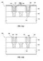
- FIG. 1( a )depicts a simplified partial cross-sectional view of a semiconductor device structure 100 including a semiconductor substrate 110 preparatory to forming a self-aligned contact between two conductive damascene lines.
- FIG. 1( a )depicts a simplified partial cross-sectional view of a semiconductor device structure 100 including a semiconductor substrate 110 preparatory to forming a self-aligned contact between two conductive damascene lines.
- FIG. 1( a )depicts a simplified partial cross-sectional view of a semiconductor device structure 100 including a semiconductor substrate 110 preparatory to forming a self-aligned contact between two conductive damascene lines.
- FIG. 1( a )depicts a simplified partial cross-sectional view of a semiconductor device structure 100 including
- FIG. 1( a )depicts a simplified cross-sectional view of a substrate 110 , preferably, a semiconductor substrate, such as a full or partial wafer of silicon, gallium arsenide, indium phosphide, or another semiconductive material, or another known type of large-scale semiconductor substrate, such as silicon-on-glass (SOG) (which may be doped or undoped), silicon-on-sapphire (SOS), silicon-on-ceramic (SOC), or other silicon-on-insulator (SOI) type substrate.
- SOGsilicon-on-glass
- SOSsilicon-on-sapphire
- SOCsilicon-on-ceramic
- SOIsilicon-on-insulator
- a first insulation layer 120 with one or more conductive structures 125such as conductive plugs, extending therethrough may be located over the substrate 110 .
- Conductive structures 125may be configured to extend to both an upper surface 122 and a lower surface 124 of the first insulation layer 120 .
- the first insulation layer 120may comprise any suitable dielectric material and may include one layer or multiple sublayers.
- the dielectric material of the first insulation layer 120may include a film 121 of doped silicon oxide, such as spin-on glass (SOG), borophosphosilicate glass (BPSG), borosilicate glass (BSG), or phosphosilicate glass (PSG), or an undoped silicon dioxide.
- the silicon oxide film 121may be provided as a base film with a thin film 123 including silicon nitride or another nitride-containing material thereover.
- the materials of the first insulation layer 120may be formed by known methods, such as by chemical vapor deposition (CVD), spin-on processes, or any other method known in the art.
- the conductive structures 125may also be formed by known processes, either before or after (e.g., by patterning films 121 and 123 and introducing conductive material into recesses formed therein) the first insulation layer 120 is formed.
- the first insulation layer 120 and, optionally, any conductive structures 125 therein,may be planarized, as known in the art (e.g., by known chemical mechanical polishing (CMP) techniques, use of SOG processes, or by dry etch-back techniques).
- CMPchemical mechanical polishing
- another insulation layer 130is formed over the substrate 110 and in contact with surface 122 of insulation layer 120 of the semiconductor device structure 100 .
- the insulation layer 130may be formed from any dielectric material, such as BPSG, BSG, PSG, another doped silicon dioxide, an undoped silicon dioxide, or SOG.
- the insulation layer 130may comprise one layer or multiple layers and may be deposited by known methods, such as those described previously herein with respect to insulation layer 120 .
- An upper, or active, surface 132 of the second insulation layer 130may be planarized (e.g., by CMP techniques) to impart the insulation layer 130 with a thickness which is about the same as the desired height of conductive structures to be subsequently formed therein and extend therethrough (e.g., in the range of about 1000 angstroms to about 10,000 angstroms).
- insulation layer 130may be patterned by known techniques (e.g., by employing a photoresist mask with openings formed therein (not shown) and etching the second insulation layer 130 through the mask).
- openings 140may be formed in the upper surface 132 of the second insulation layer 130 by anisotropic, or dry, etch processes, such as by plasma etching.
- the openings 140may comprise, for example, trenches for conductive lines or vias. As illustrated, the openings 140 are formed in a manner that exposes the conductive structures 125 .
- the photoresist maskmay be removed to provide the structure depicted in FIG. 1( a ).
- a first portion of a protective lining 150is formed by fabricating spacers 152 on at least side walls 142 of the openings 140 .
- the spacers 152may be formed with any known, suitable insulative material (e.g., silicon nitride, undoped silicon dioxide, Al 2 O 3 , Ta 2 O 5 , etc.).
- the spacers 152are preferably formed from a material that resists etching by certain etchants that may be used to remove material of the laterally adjacent insulation layer 130 . For example, when a doped silicon dioxide is used to form insulation layer 130 , silicon nitride or undoped silicon dioxide may be used to form spacers 152 .
- spacer 152 materialmay be substantially conformably deposited over the upper surface 132 of the insulation layer 130 , including on the surfaces of side walls 142 , then removed from surface 132 by known processes (e.g., masking and etching or CMP) to leave insulative material on the side walls 142 and to thereby form the spacers 152 .
- CVD processese.g., CVD processes.
- a layer 156 of conductive materialis deposited over the insulation layer 130 , filling the openings 140 .
- Layer 156may be formed by any suitable method for the particular type of conductive material employed, including, but not limited to, sputtering, CVD, physical vapor deposition (PVD), plating, electroplating, or other techniques known in the art.
- any suitable conductive materialmay be used to form layer 156 , including, without limitation, copper, aluminum, titanium, titanium nitride, tungsten, tungsten nitride, tantalum, tantalum nitride, platinum, ruthenium, rhodium, iridium, osmium, another metal, any combination or alloy of the foregoing metals and metal alloys, a metal silicide or polycide, such as tungsten silicide, molybdenum silicide, tantalum silicide, or titanium silicide, or conductively doped polycrystalline silicon, or “polysilicon.”
- Layer 156may comprise one or more sublayers 156 a , 156 b .
- Layer 156preferably has a thickness sufficient to substantially fill the openings 140 .
- sublayers 156 a and 156 b of titanium and a titanium alloyare used to fill openings 140 having depths of about 500 angstroms to about 8,000 angstroms.
- the sublayer 156 a of titaniummay be deposited to a thickness in the range of about 50 angstroms to about 300 angstroms, with 150 angstroms currently being preferred.
- Depositing a titanium layer 156 a of for example, about 150 angstromswill result in a layer overlying the spacers 152 and the bottom surface 143 of the openings 140 .
- Another sublayer 156 b of titanium nitridemay then be deposited to a suitable thickness to substantially fill the openings 140 .
- the conductive material of layer 156may overlie the upper surface 132 of the insulation layer 130 . Accordingly, conductive material remaining on the upper surface 132 may be removed therefrom by known processes, such as planarization (e.g., by CMP) or known etching techniques, thereby forming conductive structures 160 , such as damascene lines, in the openings 140 , as shown in FIG. 1( d ).
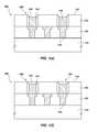
- An upper portion 147 of the conductive structures 160 in the openings 140may be removed, as shown in FIG. 1( e ), so as to facilitate the alignment of a subsequently fabricated insulative cap 154 ( FIG. 1( f )) over each of the conductive structures 160 .
- an etch-back techniquemay be employed, such as an anisotropic, or dry, etch or a wet etch that etches the material of layer 156 with selectivity over the materials of the spacers 152 and the insulation layer 130 , as known in the art. This etch-back may be accomplished substantially concurrently with the removal of conductive material from the upper surface 132 of the insulation layer 130 , or as a separate (i.e., either prior or subsequent) process.
- the etch-back of the upper portion 147 of the conductive structures 160recesses the conductive structures 160 relative to the upper surface 132 of the insulation layer 130 , providing a recessed area 148 above each of the conductive structures 160 .
- an insulative cap 154may be formed within each recessed area 148 so as to substantially insulate the corresponding conductive structure 160 .
- Insulative cap 154may be formed by any suitable, known technique, including, without limitation, by forming a layer of insulative material over the insulation layer 130 so as to substantially fill the recessed areas 148 and cover the upper surface 132 of the insulation layer 130 . Any of the insulative material that overlies the upper surface 132 of the insulation layer 130 may be removed therefrom by known techniques, such as by known polishing or planarization processes or by known etching techniques. Accordingly, the insulative material of the layer remains only over the conductive structures 160 , forming the insulative caps 154 thereover.
- the insulative caps 154may be formed from an insulative material that is not substantially etched when the insulative material of the insulation layer 130 is removed by selective etching processes. For example, if a doped silicon dioxide (e.g., BPSG, BSG, PSG, etc.) or SOG is used to form the insulation layer 130 , silicon nitride, undoped silicon dioxide, Al 2 O 3 , Ta 2 O 5 , or other suitable materials may be used to form the insulative caps 154 over the conductive structures 160 .
- the insulative material of the insulative caps 154may be the same material as that used to form the spacers 152 that are disposed laterally adjacent the conductive structures 160 .
- the exposed surfaces of the insulative caps 154may be located in substantially the same plane as that in which the upper surface 132 of the insulation layer 130 is located. With this arrangement, the conductive structures 160 and their corresponding spacers 152 and insulative caps 154 form an insulated conductive structure that is associated with a corresponding, underlying conductive structure 125 , as desired.
- Insulation layer 170may be formed by any suitable, known method (e.g., by CVD).
- An electrically insulative materiale.g., doped silicon dioxide, undoped silicon dioxide, or SOG
- SOGelectrically insulative material that may be etched with the material from which the insulation layer 130 is formed without the material or materials of other structures, such as spacers 152 or insulative caps 154 , may be used to form the insulation layer 170 .
- a photoresist 180may be provided over insulation layer 170 and the insulation layer patterned therethrough, as known in the art, to form apertures 182 through the insulation layer 170 .
- the apertures 182are preferably aligned over the region 184 of insulation layer 130 located between the conductive structures 160 , over at least one of the conductive structures 125 underlying the insulation layer 130 , and at least partially over the side walls that are laterally adjacent to region 184 , but the apertures 182 preferably do not extend over the conductive structures 160 .
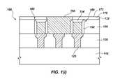
- the insulative material 130 and 170 within region 184is removed to provide a self-aligned opening 190 in insulation layer 130 .
- the self-aligned opening 190at least partially exposes at least one conductive structure 125 .
- the spacers 152are partially exposed in self-aligned opening 190 and will also subsequently serve as the side walls of a conductive structure 195 (see FIG. 1( i )) to be formed in the self-aligned opening 190 .
- the self-aligned opening 190may be formed by known wet etch or dry etch techniques. If etchants are used to form self-aligned opening 190 , the etchants are preferably selected for their ability to remove the insulative material of the insulation layers 130 and 170 with selectivity over, or at a faster rate than, the material of spacers 152 and insulative caps 154 is removed. For example, hydrofluoric acid (HF) is useful for removing doped silicon dioxide with selectivity over both silicon nitride and undoped silicon oxides. As another example, the dry etchants disclosed in U.S. Pat. No.
- HFhydrofluoric acid
- the self-aligned opening 190may be a trench configured to hold a conductive line, a via configured to receive a conductive plug, or any other type of recess configured to at least partially contain a conductive structure.
- the configuration of self-aligned opening 190may be determined by the configuration of the apertures 182 that were previously formed in the photoresist 180 . As such, the configuration of self-aligned opening 190 may be easily defined, adjusted or changed by simply adjusting the configuration of the corresponding aperture 182 (see FIG. 1( g )).
- a conductive structure 195may be formed in the self-aligned opening 190 by providing a conductive material, such as those described above in reference to FIG. 1( c ), therein.
- the conductive materialmay be deposited at least into self-aligned opening 190 by CVD, PVD, plating, electroplating, or any other suitable conductive layer or conductive structure fabrication process known in the art. Any excess conductive material remaining over an upper surface 172 of insulation layer 170 or over the upper surface 132 of insulation layer 130 may be removed therefrom by known processes (e.g., by planarization, polishing or etching the material therefrom).
- the upper surface of conductive structure 195resides in substantially the same plane as the upper surface 172 of insulation layer 170 or as the upper surface 132 of insulation layer 130 .
- the conductive materialmay include, but is not limited to, aluminum, copper, titanium, titanium nitride, another suitable metal, any combination or alloy of metals, or polycrystalline silicon.
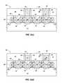
- FIGS. 2( a )- 2 ( f )another embodiment of a process that incorporates teachings of the present invention is depicted.
- the process depicted in FIGS. 2( a )- 2 ( f )is substantially the same as that described herein in reference to FIGS. 1( a )- 1 ( i ), except that the semiconductor device structure 10 includes an existing layer of transistor gates 16 , which may be fabricated by any of a series of suitable, known semiconductor device fabrication techniques.
- the semiconductor device structure 10includes a substrate 12 (e.g., a full or partial semiconductor wafer or a silicon-on-insulator type substrate, as described above in reference to FIG.
- semiconductor device structure 10includes shallow trench isolation (STI) structures as the isolation structures 14 thereof, which are recessed in the substrate 12 . Additionally, semiconductor device structure 10 includes active-device regions 18 , which comprise conductively doped regions of the substrate 12 that are laterally discrete from one another and continuous with the active surface 11 . Transistor gates 16 are formed on the active surface 11 of the substrate 12 , as well as on regions of the isolation structures 14 that are located adjacent to the active surface 11 , between adjacent active-device regions 18 . Each transistor gate 16 includes a gate oxide layer 29 , which rests upon active surface 11 and separates overlying conductive lines 22 and 24 from the active surface 11 .
- STIshallow trench isolation
- each transistor gate 16is electrically insulated from adjacent structures by way of side wall spacers 28 on each side thereof and an insulative cap 26 positioned over the uppermost conductive line 24 .
- the semiconductor device structure 10 shown in FIG. 2( a )also includes an insulation layer 30 , which covers portions of transistor gates 16 . At least some of the active-device regions 18 of the substrate 12 are electrically exposed through the insulation layer 30 by way of conductive plugs 20 that extend through the insulation layer 30 . As shown, the upper surface 19 of each conductive plug 20 has been planarized and resides in substantially the same plane as the upper surface 31 of the insulation layer 30 .
- insulation layer 32Another layer of insulative material, referred to herein as insulation layer 32 , is formed over insulation layer 30 .
- Known processessuch as CVD processes, may be used to form the insulation layer 32 .
- Doped silicon dioxides, or glassessuch as borophosphosilicate glass (BPSG), borosilicate glass (BSG), phosphosilicate glass (PSG), and spin-on glass (SOG), are examples of materials from which the insulation layer 32 may be formed.
- the insulation layer 32may be patterned (e.g., by mask and etch techniques) to form one or more openings 42 therein. Each opening 42 may, as shown, expose a corresponding conductive plug 20 .
- the side walls 43 of each opening 42may be lined with an insulative material (e.g., silicon nitride, undoped silicon dioxide, Al 2 O 3 , Ta 2 O 5 , etc.) that may resist removal by at least some etchants that will remove the material of the adjacent insulation layer 32 and, optionally, the material of insulation layer 30 .
- an insulative materiale.g., silicon nitride, undoped silicon dioxide, Al 2 O 3 , Ta 2 O 5 , etc.
- Such liningmay be effected by known deposition processes (e.g., CVD) or otherwise, as known in the art. If deposition processes are employed, it may be necessary to remove insulative material from the upper surface 33 of the insulation layer 32 .
- the resulting structuresare spacers 44 that are located adjacent to the side walls 43 of each opening 42 .
- a quantity of a suitable electrically conductive materialsuch as those described above in reference to FIG. 1( c ), may be introduced into each opening 42 to form a wiring line 21 therein.
- a suitable electrically conductive materialsuch as those described above in reference to FIG. 1( c )
- CVDchemical vapor deposition
- titanium/titanium nitride, titanium/titanium nitride/aluminum-copper alloy, or barrier layer/coppermay be used to introduce the electrically conductive material into the openings 42 . Again, it may be necessary to remove (e.g., by CMP or etching) the electrically conductive material from the upper surface 33 of the insulation layer 32 .
- FIG. 2( d )illustrates the removal of an upper portion of each wiring line 21 to recess the same beneath the plane in which the upper surface 33 of the insulation layer 32 is located.
- Such removalmay, by way of example, be effected by etching the electrically conductive material from which wiring lines 21 are formed with selectivity over the materials from which the insulation layer 32 and the spacers 44 are formed. If etching processes are also used to remove the electrically conductive material from the upper surface 33 , these acts may be effected during the same etch process.
- An insulative materialmay then be introduced (e.g., by CVD) over the wiring lines 21 and into the upper portion of each opening 42 and any excess insulative material removed from the upper surface 33 of the insulation layer 32 to form an insulative cap 23 over each wiring line 21 .
- the material from which insulative caps 23 are formedmay or may not be the same as the material from which spacers 44 are formed.
- insulation layer 25may be formed (e.g., by CVD) over insulation layer 32 and the wiring lines 21 that extend therethrough.
- insulation layer 25may be formed from a material (e.g., undoped silicon dioxide, doped silicon dioxide, etc.) that may be etched with selectivity over the material or materials from which the insulative caps 23 and spacers 44 are formed.
- a mask 27e.g., a photomask
- regions of the insulation layer 25 that are located over and laterally between adjacent wiring lines 21are exposed through mask 27 .
- the portions of the insulation layer 25 that are exposed therethroughmay be etched or otherwise removed, as known in the art and illustrated in FIG. 2( f ). Thereafter, and preferably during the same etch process, the insulative material of underlying regions of the next-lower insulation layer 32 may also be removed.
- known selective etchantsmay be used to remove the insulative material of one or both of insulation layer 25 and insulation layer 32 .
- the insulative cap 23 and spacers 44 surrounding each wiring line 21ensure that the opening, or contact 34 , which is formed by removing insulative material from insulation layer 32 , is self-aligned adjacent to at least one wiring line 21 and, preferably, as shown, between adjacent wiring lines 21 .
- the contact 34may expose a selected wiring line 21 through insulation layers 25 and 32 . Conductive material may then be introduced into each contact 34 and removed from an upper surface 35 of the insulation layer 25 to form a contact plug 36 within each contact 34 .
- An exemplary method by which this alternative structure 200 may be fabricatedis similar to the previously described embodiment with the exception that the conductive structures 295 (see FIG. 3( d )) are adjacent to only one other conductive structure 260 , such as a single damascene line, rather than between two conductive structures 160 , as in the previously described embodiment of semiconductor device structure 100 (see FIGS. 1( a )- 1 ( i )).
- semiconductor device structure 200may be fabricated using substantially the same techniques and materials as those described previously herein, with the exception that a mask must be employed to form the openings 240 in which the conductive structures 295 are to be formed.
- FIG. 3( a )depicts a semiconductor device structure 200 with a semiconductor substrate 210 and conductive structures 225 , such as the depicted conductive plugs or conductive lines, active device regions, or other circuit components, at least partially contacted by an insulation layer 230 .
- conductive structures 225are formed in an underlying insulation layer 220 , but conductive structures 225 , such as active device regions, may alternatively be formed in the substrate 210 .
- Insulation layer 230includes an opening 240 over one of the conductive structures 225 .
- At least the side walls 242 of opening 240are lined with a suitable insulative material to form spacers 252 and substantially filled with a suitable conductive material 256 so as to form another conductive structure 260 associated with the underlying conductive structures 225 .
- An insulative cap 254is formed over the conductive structure 260 .
- the insulative material of insulation layer 230is preferably selectively etchable with respect to the insulative material or materials of the side wall spacers 252 and insulative cap 254 , as described previously herein with respect to the insulative layer 130 , spacers 152 , and insulative caps 154 of the semiconductor device structure 100 depicted in FIGS. 1( a )- 1 ( i ).
- FIG. 3( b )depicts another insulation layer 270 which may be provided over insulation layer 230 .
- a photoresist layer 280 with apertures 282 formed therethroughis positioned over insulation layer 270 .
- the apertures 282 through the photoresist layer 280are aligned over at least one region 284 of the insulation layer 230 that is located laterally adjacent to the conductive structure 260 .
- the insulation layers 230 and 270may be etched through apertures 282 to form self-aligned opening 290 .
- the self-aligned opening 290may be formed by use of known dry etch or other anisotropic etch processes, which form a substantially vertical side wall 292 relative to the plane of insulation layer 230 .
- the use of known isotropic etch processes to form self-aligned opening 290are, however, also within the scope of the present invention.
- the photoresist layer 280may be removed after the self-aligned opening 290 has been formed.
- only one of the side walls 292 of each self-aligned opening 290is formed by a spacer 252 .
- only one side of the self-aligned opening 290is actually self-aligning, the other side of the self-aligned opening 290 being determined by the aperture 282 of the photoresist layer 280 .
- conductive materialsuch as one or more of those described above in reference to FIG. 1( c ), may be deposited in self-aligned opening 290 by known processes, such as by the conductive material deposition processes discussed previously herein. Any excess conductive material may be removed from upper surface 232 of insulation layer 230 or from upper surface 272 of insulation layer 270 by known processes, such as by known polishing, planarization, or etching processes. As a result, one or more conductive structures 295 are formed within self-aligned opening 290 and electrically isolated from a laterally adjacent conductive structure 260 .
- semiconductor device structure 300includes a semiconductor substrate 310 with active device regions 325 formed therein and continuous with an active surface 312 thereof.
- Transistor gate structures 340are formed on active surface 312 and include a gate oxide 344 in contact with active surface 312 and isolating an overlying conductive line 360 from substrate 310 and active surface 312 thereof.
- Each transistor gate structure 340also includes side wall spacers 352 laterally adjacent at least the conductive line 360 thereof and an insulative cap 354 disposed over the conductive line 360 thereof.
- the transistor gate structures 340are formed in an insulation layer 330 in accordance with methods of the present invention.
- the insulative material of insulation layer 330may be etched with selectivity over the insulative material or materials of side wall spacers 352 and insulative caps 354 .
- Another insulation layer 370may also be positioned over insulation layer 330 and the transistor gate structures 340 .
- a self-aligned opening 390is formed between adjacent transistor gate structures 340 by employing the methods of the present invention, as described previously herein.
- One of the active device regions 325 formed in substrate 310is at least partially exposed through the self-aligned opening 390 .
- a conductive structure 395such as a conductive contact plug, may be formed in the self-aligned opening 390 .
- Other structures of semiconductor device structure 300that overlie the portion of semiconductor device structure 300 depicted in FIG. 4 may subsequently be formed, as known in the art.
- openings in which transistor gate structures 340 are to be locatedmay be formed in insulation layer 330 , as previously described herein, so as to be laterally offset from active device regions 325 .
- At least side walls 342 of openings in which the transistor gate structures 340 are to be formedare lined with side wall spacers 352 , as described previously herein.
- the gate oxide 344 of an exemplary transistor gate structure 340may be formed by growing an oxide layer between the active device regions 325 exposed through openings in which transistor gate structures 340 are to be formed.
- a layer formed from polycrystalline silicon or another suitable conductive materiale.g., one or more of those described above in reference to FIG.
- transistor gate structure 340may be deposited at least within the openings in which transistor gate structures 340 are to be formed and over the gate oxide 344 to form conductive lines within the openings.
- the conductive materialmay then be etched back to form a recess 367 over each conductive line 360 .
- the polycrystalline siliconmay be implanted with an n-type or p-type dopant.
- a selective silicide 368may then be formed in the recess 367 over the doped polycrystalline silicon layer 366 .
- An insulative cap 354may then be formed by known processes, such as those described previously herein. It should be recognized that the described method for forming a transistor gate structure is merely exemplary.
- semiconductor device structure 400includes a semiconductor substrate 410 with a conductive line 425 thereover, as well as a plurality of damascene conductive lines 460 overlying and traversing conductive line 425 .
- the conductive elements 456 of damascene conductive lines 460are electrically isolated from the underlying conductive line 425 by way of a first insulation layer 420 overlying conductive line 425 .
- the upper and lateral surfaces of each conductive element 456are surrounded by a protective layer 450 , which includes side walls 452 adjacent the lateral surfaces of each conductive element 456 and an insulative cap 454 covering the upper surface of each conductive element 456 .
- a self-aligned opening 490is located between the side walls 452 of adjacent damascene conductive lines 460 and communicates with openings formed through an insulation layer 470 that overlies the damascene conductive lines 460 .
- a damascene conductive plug 495which communicates with the underlying conductive line 425 , is disposed in self-aligned opening 490 between adjacent damascene conductive lines 460 and electrically isolated therefrom by way of a portion of protective layer 450 .
- the remainder of each damascene conductive line 460is laterally surrounded by a second insulation layer 430 .
- the second insulation layer 430is preferably fabricated from an insulative material that is selectively etchable with respect to the insulative materials of the side walls 452 and the insulative caps 454 .
- the first insulation layer 420may be fabricated over conductive line 425 by known processes, including, without limitation, known CVD techniques, oxidation processes, and other known methods for forming layers from electrically insulative materials.
- CVD techniqueschemical vapor deposition techniques
- oxidation processesoxidation processes
- Each of the other described and illustrated features of semiconductor device structure 400 that overlies the semiconductor substrate 410may then be fabricated in the same manner as the other embodiments of semiconductor device structures described previously herein.
- the methods of the present inventioninclude forming a first conductive structure at least partially enclosed within a protective layer that is formed from materials that are able to resist removal by etchants that are used to remove adjacent portions of a different type of insulative material prior to forming an adjacent conductive structure, the margin for error or misalignment of the opening for the adjacent conductive structure is minimal.
- the protective layer formed around the damascene conductive structuresprevents the damascene conductive structures from corroding or from electrically shorting with other electrically conductive components. Also, by combining the damascene lines with the self-aligned contact, the number of steps necessary for manufacture is reduced, there is increased time efficiency, and the fabricated, adjacent conductive structures better maintain their integrity.
Landscapes
- Engineering & Computer Science (AREA)
- Physics & Mathematics (AREA)
- Condensed Matter Physics & Semiconductors (AREA)
- General Physics & Mathematics (AREA)
- Computer Hardware Design (AREA)
- Microelectronics & Electronic Packaging (AREA)
- Power Engineering (AREA)
- Manufacturing & Machinery (AREA)
- Internal Circuitry In Semiconductor Integrated Circuit Devices (AREA)
Abstract
Description
Claims (19)
Priority Applications (2)
| Application Number | Priority Date | Filing Date | Title |
|---|---|---|---|
| US13/915,210US8951910B2 (en) | 2003-03-04 | 2013-06-11 | Methods for fabricating and forming semiconductor device structures including damascene structures |
| US14/604,160US20150130080A1 (en) | 2003-03-04 | 2015-01-23 | Semiconductor device structures including damascene structures |
Applications Claiming Priority (4)
| Application Number | Priority Date | Filing Date | Title |
|---|---|---|---|
| US10/378,796US7074717B2 (en) | 2003-03-04 | 2003-03-04 | Damascene processes for forming conductive structures |
| US11/291,176US8053899B2 (en) | 2003-03-04 | 2005-11-30 | Semiconductor devices including damascene trenches with conductive structures |
| US13/237,447US8461692B2 (en) | 2003-03-04 | 2011-09-20 | Semiconductor device structures including damascene trenches with conductive structures and related method |
| US13/915,210US8951910B2 (en) | 2003-03-04 | 2013-06-11 | Methods for fabricating and forming semiconductor device structures including damascene structures |
Related Parent Applications (1)
| Application Number | Title | Priority Date | Filing Date |
|---|---|---|---|
| US13/237,447ContinuationUS8461692B2 (en) | 2003-03-04 | 2011-09-20 | Semiconductor device structures including damascene trenches with conductive structures and related method |
Related Child Applications (1)
| Application Number | Title | Priority Date | Filing Date |
|---|---|---|---|
| US14/604,160DivisionUS20150130080A1 (en) | 2003-03-04 | 2015-01-23 | Semiconductor device structures including damascene structures |
Publications (2)
| Publication Number | Publication Date |
|---|---|
| US20130277721A1 US20130277721A1 (en) | 2013-10-24 |
| US8951910B2true US8951910B2 (en) | 2015-02-10 |
Family
ID=32926560
Family Applications (5)
| Application Number | Title | Priority Date | Filing Date |
|---|---|---|---|
| US10/378,796Expired - LifetimeUS7074717B2 (en) | 2003-03-04 | 2003-03-04 | Damascene processes for forming conductive structures |
| US11/291,176Expired - Fee RelatedUS8053899B2 (en) | 2003-03-04 | 2005-11-30 | Semiconductor devices including damascene trenches with conductive structures |
| US13/237,447Expired - Fee RelatedUS8461692B2 (en) | 2003-03-04 | 2011-09-20 | Semiconductor device structures including damascene trenches with conductive structures and related method |
| US13/915,210Expired - LifetimeUS8951910B2 (en) | 2003-03-04 | 2013-06-11 | Methods for fabricating and forming semiconductor device structures including damascene structures |
| US14/604,160AbandonedUS20150130080A1 (en) | 2003-03-04 | 2015-01-23 | Semiconductor device structures including damascene structures |
Family Applications Before (3)
| Application Number | Title | Priority Date | Filing Date |
|---|---|---|---|
| US10/378,796Expired - LifetimeUS7074717B2 (en) | 2003-03-04 | 2003-03-04 | Damascene processes for forming conductive structures |
| US11/291,176Expired - Fee RelatedUS8053899B2 (en) | 2003-03-04 | 2005-11-30 | Semiconductor devices including damascene trenches with conductive structures |
| US13/237,447Expired - Fee RelatedUS8461692B2 (en) | 2003-03-04 | 2011-09-20 | Semiconductor device structures including damascene trenches with conductive structures and related method |
Family Applications After (1)
| Application Number | Title | Priority Date | Filing Date |
|---|---|---|---|
| US14/604,160AbandonedUS20150130080A1 (en) | 2003-03-04 | 2015-01-23 | Semiconductor device structures including damascene structures |
Country Status (1)
| Country | Link |
|---|---|
| US (5) | US7074717B2 (en) |
Cited By (1)
| Publication number | Priority date | Publication date | Assignee | Title |
|---|---|---|---|---|
| CN110610903A (en)* | 2018-06-15 | 2019-12-24 | 台湾积体电路制造股份有限公司 | Manufacturing method of semiconductor device |
Families Citing this family (29)
| Publication number | Priority date | Publication date | Assignee | Title |
|---|---|---|---|---|
| US7074717B2 (en) | 2003-03-04 | 2006-07-11 | Micron Technology, Inc. | Damascene processes for forming conductive structures |
| US20060034012A1 (en)* | 2003-08-29 | 2006-02-16 | Lam Terence T | Self-aligned coil process in magnetic recording heads |
| KR100625188B1 (en)* | 2005-05-10 | 2006-09-15 | 삼성전자주식회사 | Manufacturing method of semiconductor device |
| KR100635925B1 (en)* | 2005-07-21 | 2006-10-18 | 삼성전자주식회사 | Wiring structure of semiconductor device and method for forming same |
| US7666776B2 (en)* | 2005-09-01 | 2010-02-23 | Micron Technology, Inc. | Methods of forming conductive structures |
| US20070202677A1 (en)* | 2006-02-27 | 2007-08-30 | Micron Technology, Inc. | Contact formation |
| KR100833423B1 (en)* | 2006-04-06 | 2008-05-29 | 주식회사 하이닉스반도체 | Manufacturing method of semiconductor device |
| US8980756B2 (en) | 2007-07-30 | 2015-03-17 | Micron Technology, Inc. | Methods for device fabrication using pitch reduction |
| US8207041B2 (en) | 2010-03-09 | 2012-06-26 | Micron Technology, Inc. | Semiconductor processing methods |
| US9406621B2 (en)* | 2010-06-10 | 2016-08-02 | Texas Instruments Incorporated | Ultraviolet energy shield for non-volatile charge storage memory |
| DE102011101035B4 (en)* | 2011-05-10 | 2014-07-10 | Infineon Technologies Ag | A method of manufacturing a terminal region on a sidewall of a semiconductor body |
| KR20130007378A (en)* | 2011-07-01 | 2013-01-18 | 삼성전자주식회사 | Semiconductor device |
| KR20130118095A (en)* | 2012-04-19 | 2013-10-29 | 에스케이하이닉스 주식회사 | Resistance variable memory device and method for fabricating the same |
| US9299740B2 (en)* | 2012-05-31 | 2016-03-29 | Taiwan Semiconductor Manufacturing Company, Ltd. | Image sensor with low step height between back-side metal and pixel array |
| US8803321B2 (en) | 2012-06-07 | 2014-08-12 | International Business Machines Corporation | Dual damascene dual alignment interconnect scheme |
| US8975138B2 (en)* | 2013-06-28 | 2015-03-10 | Intel Corporation | Method of creating a maskless air gap in back end interconnects with double self-aligned vias |
| KR102094476B1 (en)* | 2013-08-27 | 2020-03-30 | 삼성전자주식회사 | Semiconductor device and method of manufacturing the semiconductor device |
| US9331038B2 (en)* | 2013-08-29 | 2016-05-03 | Taiwan Semiconductor Manufacturing Company Ltd. | Semiconductor interconnect structure |
| US9379058B2 (en) | 2014-02-14 | 2016-06-28 | Qualcomm Incorporated | Grounding dummy gate in scaled layout design |
| US10998228B2 (en) | 2014-06-12 | 2021-05-04 | Taiwan Semiconductor Manufacturing Company, Ltd. | Self-aligned interconnect with protection layer |
| US9716035B2 (en)* | 2014-06-20 | 2017-07-25 | Taiwan Semiconductor Manufacturing Company, Ltd. | Combination interconnect structure and methods of forming same |
| US20160005822A1 (en)* | 2014-07-01 | 2016-01-07 | Qualcomm Incorporated | Self-aligned via for gate contact of semiconductor devices |
| US9502286B2 (en)* | 2014-12-05 | 2016-11-22 | Globalfoundries Inc. | Methods of forming self-aligned contact structures on semiconductor devices and the resulting devices |
| CN107452680B (en)* | 2016-06-01 | 2020-05-05 | 中芯国际集成电路制造(上海)有限公司 | Semiconductor device and method of manufacturing the same |
| US10109526B1 (en)* | 2017-05-31 | 2018-10-23 | Globalfoundries Inc. | Etch profile control during skip via formation |
| US10559470B2 (en)* | 2018-01-22 | 2020-02-11 | Globalfoundries Inc. | Capping structure |
| US10833010B2 (en) | 2018-10-31 | 2020-11-10 | International Business Machines Corporation | Integration of artificial intelligence devices |
| US11257753B2 (en)* | 2020-01-21 | 2022-02-22 | Taiwan Semiconductor Manufacturing Company Ltd. | Interconnect structure and method for manufacturing the interconnect structure |
| US12334442B2 (en)* | 2022-08-31 | 2025-06-17 | International Business Machines Corporation | Dielectric caps for power and signal line routing |
Citations (32)
| Publication number | Priority date | Publication date | Assignee | Title |
|---|---|---|---|---|
| US5126006A (en) | 1990-10-30 | 1992-06-30 | International Business Machines Corp. | Plural level chip masking |
| US5250457A (en) | 1992-02-19 | 1993-10-05 | Micron Technology, Inc. | Method of forming a buried bit line array of memory cells |
| US5338700A (en) | 1993-04-14 | 1994-08-16 | Micron Semiconductor, Inc. | Method of forming a bit line over capacitor array of memory cells |
| US5595937A (en) | 1995-04-13 | 1997-01-21 | Nec Corporation | Method for fabricating semiconductor device with interconnections buried in trenches |
| US5598027A (en) | 1992-06-24 | 1997-01-28 | Mitsubishi Denki Kabushiki Kaisha | Semiconductor device and method of fabricating the same |
| US5612254A (en) | 1992-06-29 | 1997-03-18 | Intel Corporation | Methods of forming an interconnect on a semiconductor substrate |
| US5629238A (en)* | 1994-11-30 | 1997-05-13 | Samsung Electronics Co., Ltd. | Method for forming conductive line of semiconductor device |
| US5635432A (en) | 1995-07-11 | 1997-06-03 | Ngk Insulators, Ltd. | High-strength silicon nitride sintered body |
| US5728595A (en) | 1995-02-22 | 1998-03-17 | Nec Corporation | Method of fabricating a self-aligned contact hole for a semiconductor device |
| US5795823A (en) | 1995-06-07 | 1998-08-18 | Advanced Micro Devices, Inc. | Self aligned via dual damascene |
| US5858877A (en) | 1992-07-28 | 1999-01-12 | Micron Technology, Inc. | Self-aligned process for making contacts to silicon substrates during the manufacture of integrated circuits therein |
| US5990524A (en) | 1997-12-18 | 1999-11-23 | Advanced Micro Devices, Inc. | Silicon oxime spacer for preventing over-etching during local interconnect formation |
| US5990011A (en) | 1997-09-18 | 1999-11-23 | Micron Technology, Inc. | Titanium aluminum alloy wetting layer for improved aluminum filling of damescene trenches |
| US6060386A (en) | 1997-08-21 | 2000-05-09 | Micron Technology, Inc. | Method and apparatus for forming features in holes, trenches and other voids in the manufacturing of microelectronic devices |
| US6077733A (en) | 1999-09-03 | 2000-06-20 | Taiwan Semiconductor Manufacturing Company | Method of manufacturing self-aligned T-shaped gate through dual damascene |
| US6080655A (en) | 1997-08-21 | 2000-06-27 | Micron Technology, Inc. | Method for fabricating conductive components in microelectronic devices and substrate structures thereof |
| US6117791A (en) | 1998-06-22 | 2000-09-12 | Micron Technology, Inc. | Etchant with selectivity for doped silicon dioxide over undoped silicon dioxide and silicon nitride, processes which employ the etchant, and structures formed thereby |
| US6133144A (en) | 1999-08-06 | 2000-10-17 | Taiwan Semiconductor Manufacturing Company | Self aligned dual damascene process and structure with low parasitic capacitance |
| US6245669B1 (en) | 1999-02-05 | 2001-06-12 | Taiwan Semiconductor Manufacturing Company | High selectivity Si-rich SiON etch-stop layer |
| US6248643B1 (en) | 1999-04-02 | 2001-06-19 | Vanguard International Semiconductor Corporation | Method of fabricating a self-aligned contact |
| US6265779B1 (en) | 1998-08-11 | 2001-07-24 | International Business Machines Corporation | Method and material for integration of fuorine-containing low-k dielectrics |
| US6323118B1 (en) | 1998-07-13 | 2001-11-27 | Taiwan Semiconductor For Manufacturing Company | Borderless dual damascene contact |
| US20010052614A1 (en) | 2000-06-16 | 2001-12-20 | Shigeru Ishibashi | Semiconductor memory provided with vertical transistor and method of manufacturing the same |
| US20010055842A1 (en) | 2000-03-09 | 2001-12-27 | Hyung-Soo Uh | Methods of forming self-aligned contact pads using a damascene gate process |
| US20020008324A1 (en)* | 2000-07-21 | 2002-01-24 | Mitsubishi Denki Kabushiki Kaisha | Semiconductor device and method of manufacturing same |
| US6348411B1 (en) | 1998-09-03 | 2002-02-19 | Micron Technology, Inc. | Method of making a contact structure |
| US6359301B1 (en)* | 1997-06-25 | 2002-03-19 | Sony Corporation | Semiconductor device and method of manufacturing the same |
| US6380082B2 (en) | 1998-12-16 | 2002-04-30 | United Microelectronics Corp. | Method of fabricating Cu interconnects with reduced Cu contamination |
| US6433381B2 (en) | 2000-07-31 | 2002-08-13 | Fujitsu Limited | Semiconductor device and method of manufacturing the same |
| US6579785B2 (en) | 2000-01-25 | 2003-06-17 | Kabushiki Kaisha Toshiba | Method of making multi-level wiring in a semiconductor device |
| US7074717B2 (en) | 2003-03-04 | 2006-07-11 | Micron Technology, Inc. | Damascene processes for forming conductive structures |
| US7183222B2 (en) | 2000-09-01 | 2007-02-27 | Cypress Semiconductor Corporation | Dual damascene structure and method of making |
Family Cites Families (1)
| Publication number | Priority date | Publication date | Assignee | Title |
|---|---|---|---|---|
| US5879986A (en)* | 1998-02-27 | 1999-03-09 | Vangaurd International Semiconductor Corporation | Method for fabrication of a one gigabit capacitor over bit line DRAM cell with an area equal to eight times the used minimum feature |
- 2003
- 2003-03-04USUS10/378,796patent/US7074717B2/ennot_activeExpired - Lifetime
- 2005
- 2005-11-30USUS11/291,176patent/US8053899B2/ennot_activeExpired - Fee Related
- 2011
- 2011-09-20USUS13/237,447patent/US8461692B2/ennot_activeExpired - Fee Related
- 2013
- 2013-06-11USUS13/915,210patent/US8951910B2/ennot_activeExpired - Lifetime
- 2015
- 2015-01-23USUS14/604,160patent/US20150130080A1/ennot_activeAbandoned
Patent Citations (35)
| Publication number | Priority date | Publication date | Assignee | Title |
|---|---|---|---|---|
| US5126006A (en) | 1990-10-30 | 1992-06-30 | International Business Machines Corp. | Plural level chip masking |
| US5250457A (en) | 1992-02-19 | 1993-10-05 | Micron Technology, Inc. | Method of forming a buried bit line array of memory cells |
| US5598027A (en) | 1992-06-24 | 1997-01-28 | Mitsubishi Denki Kabushiki Kaisha | Semiconductor device and method of fabricating the same |
| US5612254A (en) | 1992-06-29 | 1997-03-18 | Intel Corporation | Methods of forming an interconnect on a semiconductor substrate |
| US5858877A (en) | 1992-07-28 | 1999-01-12 | Micron Technology, Inc. | Self-aligned process for making contacts to silicon substrates during the manufacture of integrated circuits therein |
| US5338700A (en) | 1993-04-14 | 1994-08-16 | Micron Semiconductor, Inc. | Method of forming a bit line over capacitor array of memory cells |
| US5629238A (en)* | 1994-11-30 | 1997-05-13 | Samsung Electronics Co., Ltd. | Method for forming conductive line of semiconductor device |
| US5728595A (en) | 1995-02-22 | 1998-03-17 | Nec Corporation | Method of fabricating a self-aligned contact hole for a semiconductor device |
| US5595937A (en) | 1995-04-13 | 1997-01-21 | Nec Corporation | Method for fabricating semiconductor device with interconnections buried in trenches |
| US5795823A (en) | 1995-06-07 | 1998-08-18 | Advanced Micro Devices, Inc. | Self aligned via dual damascene |
| US5635432A (en) | 1995-07-11 | 1997-06-03 | Ngk Insulators, Ltd. | High-strength silicon nitride sintered body |
| US6359301B1 (en)* | 1997-06-25 | 2002-03-19 | Sony Corporation | Semiconductor device and method of manufacturing the same |
| US6060386A (en) | 1997-08-21 | 2000-05-09 | Micron Technology, Inc. | Method and apparatus for forming features in holes, trenches and other voids in the manufacturing of microelectronic devices |
| US6080655A (en) | 1997-08-21 | 2000-06-27 | Micron Technology, Inc. | Method for fabricating conductive components in microelectronic devices and substrate structures thereof |
| US5990011A (en) | 1997-09-18 | 1999-11-23 | Micron Technology, Inc. | Titanium aluminum alloy wetting layer for improved aluminum filling of damescene trenches |
| US5990524A (en) | 1997-12-18 | 1999-11-23 | Advanced Micro Devices, Inc. | Silicon oxime spacer for preventing over-etching during local interconnect formation |
| US6117791A (en) | 1998-06-22 | 2000-09-12 | Micron Technology, Inc. | Etchant with selectivity for doped silicon dioxide over undoped silicon dioxide and silicon nitride, processes which employ the etchant, and structures formed thereby |
| US6323118B1 (en) | 1998-07-13 | 2001-11-27 | Taiwan Semiconductor For Manufacturing Company | Borderless dual damascene contact |
| US6265779B1 (en) | 1998-08-11 | 2001-07-24 | International Business Machines Corporation | Method and material for integration of fuorine-containing low-k dielectrics |
| US6348411B1 (en) | 1998-09-03 | 2002-02-19 | Micron Technology, Inc. | Method of making a contact structure |
| US6380082B2 (en) | 1998-12-16 | 2002-04-30 | United Microelectronics Corp. | Method of fabricating Cu interconnects with reduced Cu contamination |
| US6245669B1 (en) | 1999-02-05 | 2001-06-12 | Taiwan Semiconductor Manufacturing Company | High selectivity Si-rich SiON etch-stop layer |
| US6316348B1 (en) | 1999-02-05 | 2001-11-13 | Taiwan Semiconductor Manufacturing Company | High selectivity Si-rich SiON etch-stop layer |
| US6248643B1 (en) | 1999-04-02 | 2001-06-19 | Vanguard International Semiconductor Corporation | Method of fabricating a self-aligned contact |
| US6133144A (en) | 1999-08-06 | 2000-10-17 | Taiwan Semiconductor Manufacturing Company | Self aligned dual damascene process and structure with low parasitic capacitance |
| US6077733A (en) | 1999-09-03 | 2000-06-20 | Taiwan Semiconductor Manufacturing Company | Method of manufacturing self-aligned T-shaped gate through dual damascene |
| US6579785B2 (en) | 2000-01-25 | 2003-06-17 | Kabushiki Kaisha Toshiba | Method of making multi-level wiring in a semiconductor device |
| US20010055842A1 (en) | 2000-03-09 | 2001-12-27 | Hyung-Soo Uh | Methods of forming self-aligned contact pads using a damascene gate process |
| US20010052614A1 (en) | 2000-06-16 | 2001-12-20 | Shigeru Ishibashi | Semiconductor memory provided with vertical transistor and method of manufacturing the same |
| US20020008324A1 (en)* | 2000-07-21 | 2002-01-24 | Mitsubishi Denki Kabushiki Kaisha | Semiconductor device and method of manufacturing same |
| US6433381B2 (en) | 2000-07-31 | 2002-08-13 | Fujitsu Limited | Semiconductor device and method of manufacturing the same |
| US7183222B2 (en) | 2000-09-01 | 2007-02-27 | Cypress Semiconductor Corporation | Dual damascene structure and method of making |
| US7074717B2 (en) | 2003-03-04 | 2006-07-11 | Micron Technology, Inc. | Damascene processes for forming conductive structures |
| US8053899B2 (en) | 2003-03-04 | 2011-11-08 | Micron Technology, Inc. | Semiconductor devices including damascene trenches with conductive structures |
| US20120007209A1 (en) | 2003-03-04 | 2012-01-12 | Micron Technology, Inc. | Semiconductor device structures including damascene trenches with conductive structures and related method |
Non-Patent Citations (2)
| Title |
|---|
| Kaanta et al., Dual Damascene: A ULSI Wiring Technology, VMIC Conference, Jun. 11-12, 1991, pp. 144-152. |
| Licata et al., Dual Damascene Al Wiring for 256M DRAM, VMIC Conference, Jun. 27-29, 1995, pp. 596-602. |
Cited By (6)
| Publication number | Priority date | Publication date | Assignee | Title |
|---|---|---|---|---|
| CN110610903A (en)* | 2018-06-15 | 2019-12-24 | 台湾积体电路制造股份有限公司 | Manufacturing method of semiconductor device |
| US11476156B2 (en)* | 2018-06-15 | 2022-10-18 | Taiwan Semiconductor Manufacturing Co., Ltd. | Semiconductor device structures |
| US20220399227A1 (en)* | 2018-06-15 | 2022-12-15 | Taiwan Semiconductor Manufacturing Co., Ltd. | Semiconductor Device Structures |
| US12027415B2 (en)* | 2018-06-15 | 2024-07-02 | Taiwan Semiconductor Manufacturing Co., Ltd. | Semiconductor device structures |
| CN110610903B (en)* | 2018-06-15 | 2025-06-24 | 台湾积体电路制造股份有限公司 | Semiconductor device and method for manufacturing the same |
| US12362229B2 (en)* | 2018-06-15 | 2025-07-15 | Taiwan Semiconductor Manufacturing Co., Ltd. | Semiconductor device structures |
Also Published As
| Publication number | Publication date |
|---|---|
| US20120007209A1 (en) | 2012-01-12 |
| US20040173912A1 (en) | 2004-09-09 |
| US8461692B2 (en) | 2013-06-11 |
| US20150130080A1 (en) | 2015-05-14 |
| US8053899B2 (en) | 2011-11-08 |
| US20060076689A1 (en) | 2006-04-13 |
| US20130277721A1 (en) | 2013-10-24 |
| US7074717B2 (en) | 2006-07-11 |
Similar Documents
| Publication | Publication Date | Title |
|---|---|---|
| US8951910B2 (en) | Methods for fabricating and forming semiconductor device structures including damascene structures | |
| US6800549B2 (en) | Method of fabricating semiconductor device including forming contact hole with anisotropic and isotropic etching and forming discontinuous barrier layer | |
| US5798568A (en) | Semiconductor component with multi-level interconnect system and method of manufacture | |
| US7563710B2 (en) | Method of fabrication of interconnect structures | |
| US6037255A (en) | Method for making integrated circuit having polymer interlayer dielectric | |
| EP1532679B1 (en) | Self-aligned contacts to gates | |
| US6177329B1 (en) | Integrated circuit structures having gas pockets and method for forming integrated circuit structures having gas pockets | |
| US7393777B2 (en) | Sacrificial metal spacer damascene process | |
| US6133139A (en) | Self-aligned composite insulator with sub-half-micron multilevel high density electrical interconnections and process thereof | |
| US6426249B1 (en) | Buried metal dual damascene plate capacitor | |
| US6191484B1 (en) | Method of forming planarized multilevel metallization in an integrated circuit | |
| US6121146A (en) | Method for forming contact plugs of a semiconductor device | |
| US6576550B1 (en) | ‘Via first’ dual damascene process for copper metallization | |
| US6348734B1 (en) | Self-aligned copper interconnect architecture with enhanced copper diffusion barrier | |
| US20020048944A1 (en) | Multi-level circuit structure | |
| US6066560A (en) | Non-linear circuit elements on integrated circuits | |
| US6352920B1 (en) | Process of manufacturing semiconductor device | |
| US6080663A (en) | Dual damascene | |
| US6362527B1 (en) | Borderless vias on bottom metal | |
| US6849536B2 (en) | Inter-metal dielectric patterns and method of forming the same | |
| EP1317771B1 (en) | Improved semiconductor structure and method of fabrication | |
| EP1317772B1 (en) | Semiconductor interconnection structure and method of fabrication | |
| US6319813B1 (en) | Semiconductor processing methods of forming integrated circuitry and integrated circuitry constructions | |
| US7112537B2 (en) | Method of fabricating interconnection structure of semiconductor device | |
| US6297144B1 (en) | Damascene local interconnect process |
Legal Events
| Date | Code | Title | Description |
|---|---|---|---|
| FEPP | Fee payment procedure | Free format text:PAYOR NUMBER ASSIGNED (ORIGINAL EVENT CODE: ASPN); ENTITY STATUS OF PATENT OWNER: LARGE ENTITY | |
| STCF | Information on status: patent grant | Free format text:PATENTED CASE | |
| CC | Certificate of correction | ||
| AS | Assignment | Owner name:U.S. BANK NATIONAL ASSOCIATION, AS COLLATERAL AGENT, CALIFORNIA Free format text:SECURITY INTEREST;ASSIGNOR:MICRON TECHNOLOGY, INC.;REEL/FRAME:038669/0001 Effective date:20160426 Owner name:U.S. BANK NATIONAL ASSOCIATION, AS COLLATERAL AGEN Free format text:SECURITY INTEREST;ASSIGNOR:MICRON TECHNOLOGY, INC.;REEL/FRAME:038669/0001 Effective date:20160426 | |
| AS | Assignment | Owner name:MORGAN STANLEY SENIOR FUNDING, INC., AS COLLATERAL AGENT, MARYLAND Free format text:PATENT SECURITY AGREEMENT;ASSIGNOR:MICRON TECHNOLOGY, INC.;REEL/FRAME:038954/0001 Effective date:20160426 Owner name:MORGAN STANLEY SENIOR FUNDING, INC., AS COLLATERAL Free format text:PATENT SECURITY AGREEMENT;ASSIGNOR:MICRON TECHNOLOGY, INC.;REEL/FRAME:038954/0001 Effective date:20160426 | |
| AS | Assignment | Owner name:U.S. BANK NATIONAL ASSOCIATION, AS COLLATERAL AGENT, CALIFORNIA Free format text:CORRECTIVE ASSIGNMENT TO CORRECT THE REPLACE ERRONEOUSLY FILED PATENT #7358718 WITH THE CORRECT PATENT #7358178 PREVIOUSLY RECORDED ON REEL 038669 FRAME 0001. ASSIGNOR(S) HEREBY CONFIRMS THE SECURITY INTEREST;ASSIGNOR:MICRON TECHNOLOGY, INC.;REEL/FRAME:043079/0001 Effective date:20160426 Owner name:U.S. BANK NATIONAL ASSOCIATION, AS COLLATERAL AGEN Free format text:CORRECTIVE ASSIGNMENT TO CORRECT THE REPLACE ERRONEOUSLY FILED PATENT #7358718 WITH THE CORRECT PATENT #7358178 PREVIOUSLY RECORDED ON REEL 038669 FRAME 0001. ASSIGNOR(S) HEREBY CONFIRMS THE SECURITY INTEREST;ASSIGNOR:MICRON TECHNOLOGY, INC.;REEL/FRAME:043079/0001 Effective date:20160426 | |
| AS | Assignment | Owner name:JPMORGAN CHASE BANK, N.A., AS COLLATERAL AGENT, ILLINOIS Free format text:SECURITY INTEREST;ASSIGNORS:MICRON TECHNOLOGY, INC.;MICRON SEMICONDUCTOR PRODUCTS, INC.;REEL/FRAME:047540/0001 Effective date:20180703 Owner name:JPMORGAN CHASE BANK, N.A., AS COLLATERAL AGENT, IL Free format text:SECURITY INTEREST;ASSIGNORS:MICRON TECHNOLOGY, INC.;MICRON SEMICONDUCTOR PRODUCTS, INC.;REEL/FRAME:047540/0001 Effective date:20180703 | |
| MAFP | Maintenance fee payment | Free format text:PAYMENT OF MAINTENANCE FEE, 4TH YEAR, LARGE ENTITY (ORIGINAL EVENT CODE: M1551) Year of fee payment:4 | |
| AS | Assignment | Owner name:MICRON TECHNOLOGY, INC., IDAHO Free format text:RELEASE BY SECURED PARTY;ASSIGNOR:U.S. BANK NATIONAL ASSOCIATION, AS COLLATERAL AGENT;REEL/FRAME:047243/0001 Effective date:20180629 | |
| AS | Assignment | Owner name:MICRON TECHNOLOGY, INC., IDAHO Free format text:RELEASE BY SECURED PARTY;ASSIGNOR:MORGAN STANLEY SENIOR FUNDING, INC., AS COLLATERAL AGENT;REEL/FRAME:050937/0001 Effective date:20190731 | |
| AS | Assignment | Owner name:MICRON TECHNOLOGY, INC., IDAHO Free format text:RELEASE BY SECURED PARTY;ASSIGNOR:JPMORGAN CHASE BANK, N.A., AS COLLATERAL AGENT;REEL/FRAME:051028/0001 Effective date:20190731 Owner name:MICRON SEMICONDUCTOR PRODUCTS, INC., IDAHO Free format text:RELEASE BY SECURED PARTY;ASSIGNOR:JPMORGAN CHASE BANK, N.A., AS COLLATERAL AGENT;REEL/FRAME:051028/0001 Effective date:20190731 | |
| MAFP | Maintenance fee payment | Free format text:PAYMENT OF MAINTENANCE FEE, 8TH YEAR, LARGE ENTITY (ORIGINAL EVENT CODE: M1552); ENTITY STATUS OF PATENT OWNER: LARGE ENTITY Year of fee payment:8 |