US8949643B2 - Document validator with power management - Google Patents
Document validator with power managementDownload PDFInfo
- Publication number
- US8949643B2 US8949643B2US13/255,671US201013255671AUS8949643B2US 8949643 B2US8949643 B2US 8949643B2US 201013255671 AUS201013255671 AUS 201013255671AUS 8949643 B2US8949643 B2US 8949643B2
- Authority
- US
- United States
- Prior art keywords
- validator
- power
- fet
- unit
- power source
- Prior art date
- Legal status (The legal status is an assumption and is not a legal conclusion. Google has not performed a legal analysis and makes no representation as to the accuracy of the status listed.)
- Expired - Fee Related, expires
Links
Images


Classifications
- G07D11/0036—
- G—PHYSICS
- G07—CHECKING-DEVICES
- G07D—HANDLING OF COINS OR VALUABLE PAPERS, e.g. TESTING, SORTING BY DENOMINATIONS, COUNTING, DISPENSING, CHANGING OR DEPOSITING
- G07D11/00—Devices accepting coins; Devices accepting, dispensing, sorting or counting valuable papers
- G07D11/20—Controlling or monitoring the operation of devices; Data handling
- G07D11/22—Means for sensing or detection
- G07D11/0081—
- G—PHYSICS
- G07—CHECKING-DEVICES
- G07D—HANDLING OF COINS OR VALUABLE PAPERS, e.g. TESTING, SORTING BY DENOMINATIONS, COUNTING, DISPENSING, CHANGING OR DEPOSITING
- G07D11/00—Devices accepting coins; Devices accepting, dispensing, sorting or counting valuable papers
- G07D11/40—Device architecture, e.g. modular construction
Definitions
- the disclosurerelates to a device for validating documents of value (e.g., paper currency).
- valuee.g., paper currency
- Bill validatorsare used in a wide variety of applications including; vending machines, gaming machines, ticketing machines and automated teller machines.
- Bill validatorstypically include a sensing unit for sensing authenticity and denomination of inserted banknotes.
- Various types of sensing systemscan be employed by a bill validation device for example, optical sensing, magnetic sensing or a combination of both.
- Typical bill validation deviceshave power provided for operation either from the host machine or from a direct power source such as a standard AC power outlet.
- a limitation of the type of bill validator described aboveis that it is in a continuously “ON” mode and thus continually draws power either from the host machine or through a directly connected power source. As overall power consumption for a host machine is becoming more of an issue due to operation costs, there is a need to reduce such consumption.
- a low power validator for validating documents of valueis described in claim 1 .
- a method for controlling the operation of a low power validatoris described in claim 16 . Examples are described in the dependent claims.
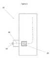
- FIG. 1illustrates an example of a banknote validator and various components.
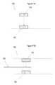
- FIG. 2illustrates an example of a banknote validator including a power management system and a power source.
- FIG. 3illustrates an example of a power management system including a wake up unit and power detecting unit.
- FIG. 4is an example of a schematic layout drawing of the wake up unit and power detection unit interconnected.
- FIG. 5 aillustrates an example of the banknote presence detection components located in the banknote validation unit inlet without a banknote present.
- FIG. 5 billustrates an example of the banknote presence detection components located in the banknote validation unit inlet with a banknote present.
- FIG. 5 cillustrates an example of the banknote presence detection components using a reflective type sensing configuration.
- FIG. 6is an example of a schematic layout of a field effect transistor (FET) used to selectively connect the power supply with the banknote validator.
- FETfield effect transistor
- the disclosurerelates to a low power validator for documents of value (e.g., paper currency validator) and, in particular, to a battery powered banknote validator including a power management system for minimizing or reducing the power consumption from a power source.
- documents of valueincludes paper currency such as banknotes and bills, as well as security documents, paper coupons and other similar documents of value (both authentic as well as unauthentic (e.g., forgeries).
- a banknote validation device 10includes an inlet 50 for receiving banknotes from a user, a transportation path 40 for conveying an inserted banknote within the bill validation device, a sensing unit 20 for sensing characteristics of an inserted banknote, and a processing unit for controlling the overall operation of the banknote validator.
- the sensing unit 20 and other componentscan be integrated, for example, within the processing unit.
- power supply unit 70is a 12-volt battery; however, other types of power supplies and voltages can be used for the power supply unit.
- Power management system 100provides control of the supply power being fed to the banknote validator. More specifically, power management system 100 controls the transfer of the banknote validator from a power saving mode to a normal operation mode. In the power saving mode, overall banknote validation system 10 draws a very low amount of power from the power supply unit. In the normal operating mode, overall banknote validation system 10 draws a normal amount of power consistent with typical banknote validator operation. In some implementations, power management system 100 is located between power supply unit 70 and banknote validator 10 . In other implementations, power management system 100 is integrated within banknote validator 10 .
- power management system 100includes a wake up unit 130 and a power detection unit 150 .
- Wake up unit 130includes a micro-controller 135 (e.g., a programmable system on chip or PSoC device) operatively connected to power source 70 , power detection unit 150 , and banknote validator 10 .
- micro-controller 135is a PSoC device.
- FIG. 4shows the interconnection of wake up unit 130 , power detection unit 150 and banknote validator 10 .
- FET 200When validator 10 is in the power saving mode, FET 200 is in a disable mode so as to not provide main power to validator 10 via line 75 . FET 200 is forced to a disable mode removing the connection of main power line 75 with validator 10 when output line 137 from microcontroller 135 becomes low.
- wake up circuit 130regularly monitors inlet 50 of banknote validator 10 for the presence of a banknote.
- the monitoring of inlet 50 for a banknotecan be done in various ways known in the art, but for the example in FIGS. 5 a and 5 b is implemented as a paired photo-emitter 81 and photo-detector 82 arranged on either side of bill path 40 .
- Emitter 81continuously emits (e.g., infrared light) across the transportation path 40 of inlet 50 such that when no banknote is present, the emitted light from emitter 81 is received by detector 82 .
- detector 82receives light from emitter 81 a banknote is not present and, therefore, measuring the signal presence of detector 82 allows for determining there is no banknote present in inlet 50 of banknote validator 10 .
- FIG. 5 bif light emitted from emitter 81 is not received by detector 82 , measuring the response signal of detector 92 allows for a determination of the presence of a banknote 90 in inlet 50 .
- a reflective object sensor configurationcan be used to detect the presence of banknote 90 in inlet 50 .
- emitter 81 and detector 82are located on the same side of banknote path 40 .
- the presence of a banknotecauses the light emitted from emitter 81 to be reflected by banknote 90 and thus received by detector 82 . Having a signal received by detector 82 allows for the measurement of the response signal of detector 82 to determine the presence of a banknote in inlet 50 as previously described.
- Wake up unit 130controls the banknote detection operation by driving emitter 81 (e.g., at a frequency of 10 Hz) and regularly samples (e.g., every 100 ms) for a received signal by detector 82 to determine if a banknote has been inserted in to inlet 50 by a user via lines 132 , 131 respectively.
- wake up unit 130drives power detection unit 150 to determine if there is enough power to transfer banknote validator 10 from the power conserving mode to the normal operation mode.
- wake up unit 130enables a drive signal (i.e., 5V) via line 154 to N-FET 152 . Receipt of a drive signal from microcontroller 135 via line 154 by N-FET 152 causes a 0V to be received by P-FET 151 and thus enable voltage to supplied to voltage divider 158 from power supply 70 .
- Voltage divider 158includes two resistors R 1 and R 2 to prevent excess voltage to be sensed by microcontroller 135 via line 155 . In the illustrated implementation, when microcontroller 135 is a PSoC device and power supply 70 is a 12V DC source, the voltage divider results is a one-third voltage reduction to comply with typical PSoC requirements.
- microcontroller 135evaluates the voltage measured over line 155 and will provide an enable signal to output line 137 .
- An enable signal on line 137 from microcontroller 135causes FET 200 to provide a connection of main power line 75 of banknote validator 10 to power supply 70 effectively transferring banknote validator 10 from a power conserving mode to a normal operation mode.
- a voltage regulatorbetween power source 70 and banknote validator 10 so as to provide a relatively constant voltage for operating banknote validator 10 .
- the inserted banknotecan be evaluated by validator 10 .
- an inserted banknote 90in transported from inlet 50 by along a transportation path 40 to sensing unit 20 .
- Sensing unit 20authenticate and/or denominates the inserted banknote and rejects non-valid banknotes back to the user by reversing the transportation mechanism of transportation path 40 so as to return the non-valid banknote through inlet 50 .
- banknote validator 10determines when to place the system back into the power conserving mode.
- the systemwill enter the power conserving mode, for example, when one of two situations exist.
- One situation that allows banknote validator 10 to transfer from the normal operating mode to the power conserving modeoccurs when the banknote validator controller sends a control signal to wake up unit 130 via line 139 .
- microcontroller 135receives a signal from the banknote validator controller to enter the power conserving mode, microcontroller 135 sends a disable signal via line 137 to FET 200 to disconnect power source 70 from banknote validator 10 .
- a disable signal received by FET 200effectively disconnects line 75 from power source 70 and banknote validator 10 .
- a second situation that allows banknote validator 10 to transfer from the normal operating mode to the power conserving modeoccurs when power source 70 is unable to provide enough power to banknote validator 10 .
- Such a situationcan arise, for example, if the voltage being sensed via line 155 falls below a predetermined threshold. Since microcontroller 135 is continuously monitoring the voltage sensed on line 155 during the normal operation mode, any drop in measured voltage of power source 70 below a predetermined threshold will cause microcontroller 135 to send a disable signal via line 137 to FET 200 , thereby disconnecting power source 70 from banknote validator 10 .
- An advantage of the power management system 100is that although banknote validator 10 cannot be transitioned from the power conserving mode to the normal operating mode when the measured voltage of power source 70 is below a predetermined threshold, if a re-charging or increase to the power source 70 voltage occurs, banknote validator 10 is able to transition at a later time between modes without having to be reset by a service person. More particularly, if the voltage of power source 70 is below a predetermined threshold, the banknote validator will remain in a power conserving mode until the voltage of power source 70 rises above the predetermined threshold, and there is no need to have to reset the system.
Landscapes
- Physics & Mathematics (AREA)
- General Physics & Mathematics (AREA)
- Power Sources (AREA)
- Inspection Of Paper Currency And Valuable Securities (AREA)
Abstract
Description
Claims (45)
Priority Applications (1)
| Application Number | Priority Date | Filing Date | Title |
|---|---|---|---|
| US13/255,671US8949643B2 (en) | 2009-03-11 | 2010-03-11 | Document validator with power management |
Applications Claiming Priority (3)
| Application Number | Priority Date | Filing Date | Title |
|---|---|---|---|
| US15937409P | 2009-03-11 | 2009-03-11 | |
| PCT/US2010/026924WO2010105022A1 (en) | 2009-03-11 | 2010-03-11 | Document validator with power management |
| US13/255,671US8949643B2 (en) | 2009-03-11 | 2010-03-11 | Document validator with power management |
Publications (2)
| Publication Number | Publication Date |
|---|---|
| US20120066533A1 US20120066533A1 (en) | 2012-03-15 |
| US8949643B2true US8949643B2 (en) | 2015-02-03 |
Family
ID=42136084
Family Applications (1)
| Application Number | Title | Priority Date | Filing Date |
|---|---|---|---|
| US13/255,671Expired - Fee RelatedUS8949643B2 (en) | 2009-03-11 | 2010-03-11 | Document validator with power management |
Country Status (4)
| Country | Link |
|---|---|
| US (1) | US8949643B2 (en) |
| EP (1) | EP2406771B1 (en) |
| ES (1) | ES2584310T3 (en) |
| WO (1) | WO2010105022A1 (en) |
Families Citing this family (2)
| Publication number | Priority date | Publication date | Assignee | Title |
|---|---|---|---|---|
| TWI478108B (en)* | 2012-09-25 | 2015-03-21 | Int Currency Tech | The Method of Directing the Location of the |
| CN115053242A (en)* | 2019-10-10 | 2022-09-13 | 克兰佩门特创新股份有限公司 | Payment receiver with multi-functional imaging sensor |
Citations (18)
| Publication number | Priority date | Publication date | Assignee | Title |
|---|---|---|---|---|
| GB2173624A (en) | 1985-04-08 | 1986-10-15 | Qonaar Corp | Low power coin discrimination apparatus |
| US5316124A (en)* | 1990-11-07 | 1994-05-31 | Mars Incorporated | Method and apparatus for a low-power, battery-powered vending and dispensing apparatus |
| US5657847A (en) | 1991-10-01 | 1997-08-19 | Innovative Technology Limited | Banknote validator |
| US6243626B1 (en)* | 1998-10-28 | 2001-06-05 | Bayview Technology Group, Inc. | External power management device with current monitoring precluding shutdown during high current |
| EP1255232A1 (en) | 2001-05-03 | 2002-11-06 | Michel Pernot | Device for banknote denomination indication |
| US6581396B2 (en) | 1998-10-28 | 2003-06-24 | Bayview Technology Group, Llc | Refrigerated vending machine exploiting expanded temperature variance during power-conservation mode |
| US6991129B2 (en) | 2003-03-14 | 2006-01-31 | International Currency Technologies Corporation | Power control circuit for use in a vending machine |
| US20060108732A1 (en)* | 2002-08-22 | 2006-05-25 | Noriyuki Kanno | Device for discriminating device |
| US7276925B2 (en)* | 2005-07-01 | 2007-10-02 | P.A. Semi, Inc. | Operating an integrated circuit at a minimum supply voltage |
| US20080070652A1 (en)* | 2006-09-18 | 2008-03-20 | Igt, Inc. | Reduced power consumption wager gaming machine |
| US20080109109A1 (en)* | 2004-02-12 | 2008-05-08 | David Schanin | Method and apparatus for conserving power consumed by a vending machine utilizing audio signal detection |
| US20080222431A1 (en)* | 2006-08-30 | 2008-09-11 | Frank Paniagua | Power Adapter Capable of Communicating Digitally with Electronic Devices |
| DE202008015252U1 (en) | 2008-11-18 | 2009-02-05 | International Currency Technologies Corporation | Bill accepting device with license recognition and power saving control functions |
| US20100178900A1 (en)* | 2009-01-09 | 2010-07-15 | Qualcomm Incorporated | Methods and systems for dynamic service flow using available battery power |
| US20100285866A1 (en)* | 2006-11-11 | 2010-11-11 | Bleich Charles R | Power conservation in wagering game machines |
| US20110217032A1 (en)* | 2006-08-10 | 2011-09-08 | Research In Motion Limited | Method and apparatus for power management in an electronic device |
| US20120075102A1 (en)* | 2006-01-27 | 2012-03-29 | Orbiter, Llc | Portable lap counter and system |
| US20130040662A1 (en)* | 2011-08-14 | 2013-02-14 | Martin Elisco | Portable communication device and method for display of black screen content |
- 2010
- 2010-03-11USUS13/255,671patent/US8949643B2/ennot_activeExpired - Fee Related
- 2010-03-11EPEP10713747.3Apatent/EP2406771B1/ennot_activeNot-in-force
- 2010-03-11ESES10713747.3Tpatent/ES2584310T3/enactiveActive
- 2010-03-11WOPCT/US2010/026924patent/WO2010105022A1/enactiveApplication Filing
Patent Citations (18)
| Publication number | Priority date | Publication date | Assignee | Title |
|---|---|---|---|---|
| GB2173624A (en) | 1985-04-08 | 1986-10-15 | Qonaar Corp | Low power coin discrimination apparatus |
| US5316124A (en)* | 1990-11-07 | 1994-05-31 | Mars Incorporated | Method and apparatus for a low-power, battery-powered vending and dispensing apparatus |
| US5657847A (en) | 1991-10-01 | 1997-08-19 | Innovative Technology Limited | Banknote validator |
| US6243626B1 (en)* | 1998-10-28 | 2001-06-05 | Bayview Technology Group, Inc. | External power management device with current monitoring precluding shutdown during high current |
| US6581396B2 (en) | 1998-10-28 | 2003-06-24 | Bayview Technology Group, Llc | Refrigerated vending machine exploiting expanded temperature variance during power-conservation mode |
| EP1255232A1 (en) | 2001-05-03 | 2002-11-06 | Michel Pernot | Device for banknote denomination indication |
| US20060108732A1 (en)* | 2002-08-22 | 2006-05-25 | Noriyuki Kanno | Device for discriminating device |
| US6991129B2 (en) | 2003-03-14 | 2006-01-31 | International Currency Technologies Corporation | Power control circuit for use in a vending machine |
| US20080109109A1 (en)* | 2004-02-12 | 2008-05-08 | David Schanin | Method and apparatus for conserving power consumed by a vending machine utilizing audio signal detection |
| US7276925B2 (en)* | 2005-07-01 | 2007-10-02 | P.A. Semi, Inc. | Operating an integrated circuit at a minimum supply voltage |
| US20120075102A1 (en)* | 2006-01-27 | 2012-03-29 | Orbiter, Llc | Portable lap counter and system |
| US20110217032A1 (en)* | 2006-08-10 | 2011-09-08 | Research In Motion Limited | Method and apparatus for power management in an electronic device |
| US20080222431A1 (en)* | 2006-08-30 | 2008-09-11 | Frank Paniagua | Power Adapter Capable of Communicating Digitally with Electronic Devices |
| US20080070652A1 (en)* | 2006-09-18 | 2008-03-20 | Igt, Inc. | Reduced power consumption wager gaming machine |
| US20100285866A1 (en)* | 2006-11-11 | 2010-11-11 | Bleich Charles R | Power conservation in wagering game machines |
| DE202008015252U1 (en) | 2008-11-18 | 2009-02-05 | International Currency Technologies Corporation | Bill accepting device with license recognition and power saving control functions |
| US20100178900A1 (en)* | 2009-01-09 | 2010-07-15 | Qualcomm Incorporated | Methods and systems for dynamic service flow using available battery power |
| US20130040662A1 (en)* | 2011-08-14 | 2013-02-14 | Martin Elisco | Portable communication device and method for display of black screen content |
Non-Patent Citations (1)
| Title |
|---|
| International Search Report dated May 21, 2010 for International Application No. PCT/US2010/026924. |
Also Published As
| Publication number | Publication date |
|---|---|
| EP2406771B1 (en) | 2016-04-27 |
| EP2406771A1 (en) | 2012-01-18 |
| ES2584310T3 (en) | 2016-09-27 |
| US20120066533A1 (en) | 2012-03-15 |
| WO2010105022A1 (en) | 2010-09-16 |
Similar Documents
| Publication | Publication Date | Title |
|---|---|---|
| US7659726B2 (en) | Image forming apparatus with plural AC sources | |
| BR112013013227B1 (en) | banknote handling device | |
| US8949643B2 (en) | Document validator with power management | |
| US8720663B2 (en) | Bill jam troubleshooting | |
| JP5862469B2 (en) | Cash processing equipment | |
| CN107808463B (en) | Apparatus, method and computer readable medium for providing power for conducting transactions | |
| EP2929515B1 (en) | Power management for an automated banking system | |
| US20030042300A1 (en) | Media sensing method for automatic media dispenser | |
| JP3909408B2 (en) | Banknote handling equipment | |
| US20100187997A1 (en) | Energy saving control for a fluorescent light in a merchandising machine and a method of retrofitting the control in a merchandising machine | |
| JP5386387B2 (en) | Automatic transaction equipment | |
| KR101111394B1 (en) | Anti-skimming system | |
| US6991129B2 (en) | Power control circuit for use in a vending machine | |
| CN107437292A (en) | Automatic teller machine with abnormal banknote processing function | |
| JP5175069B2 (en) | Paper sheet identification machine | |
| KR100354261B1 (en) | Circuit for controlling motor in apparatus for sliceing paper | |
| JP3839759B2 (en) | Currency recognition device | |
| KR101343740B1 (en) | Device for controlling a door using obstacle detection, financial device using the same and method thereof | |
| BG65191B1 (en) | System for banknotes recognition and validation | |
| US20130134011A1 (en) | Currency Cassette Capacity Monitoring And Reporting | |
| US20100155573A1 (en) | Optical sensor | |
| JP4902982B2 (en) | Method for switching operation mode of paper sheet identification device | |
| KR20080062606A (en) | Motor overload protection device | |
| JP2016004389A (en) | Bill identification device | |
| JPH0462697A (en) | banknote identification device |
Legal Events
| Date | Code | Title | Description |
|---|---|---|---|
| AS | Assignment | Owner name:MEI, INC., PENNSYLVANIA Free format text:ASSIGNMENT OF ASSIGNORS INTEREST;ASSIGNOR:MISHRA, VARUNI;REEL/FRAME:024537/0106 Effective date:20090323 | |
| AS | Assignment | Owner name:GOLDMAN SACHS BANK USA, AS COLLATERAL AGENT, NEW Y Free format text:SECURITY AGREEMENT;ASSIGNOR:MEI, INC.;REEL/FRAME:031095/0513 Effective date:20130822 | |
| AS | Assignment | Owner name:MEI, INC., PENNSYLVANIA Free format text:RELEASE OF SECURITY INTEREST IN INTELLECTUAL PROPERTY COLLATERAL RECORDED AT REEL/FRAME 031095/0513;ASSIGNOR:GOLDMAN SACHS BANK USA, AS COLLATERAL AGENT;REEL/FRAME:031796/0123 Effective date:20131211 | |
| STCF | Information on status: patent grant | Free format text:PATENTED CASE | |
| AS | Assignment | Owner name:CRANE PAYMENT INNOVATIONS, INC., PENNSYLVANIA Free format text:CHANGE OF NAME;ASSIGNOR:MEI, INC.;REEL/FRAME:036981/0237 Effective date:20150122 | |
| MAFP | Maintenance fee payment | Free format text:PAYMENT OF MAINTENANCE FEE, 4TH YEAR, LARGE ENTITY (ORIGINAL EVENT CODE: M1551) Year of fee payment:4 | |
| FEPP | Fee payment procedure | Free format text:MAINTENANCE FEE REMINDER MAILED (ORIGINAL EVENT CODE: REM.); ENTITY STATUS OF PATENT OWNER: LARGE ENTITY | |
| LAPS | Lapse for failure to pay maintenance fees | Free format text:PATENT EXPIRED FOR FAILURE TO PAY MAINTENANCE FEES (ORIGINAL EVENT CODE: EXP.); ENTITY STATUS OF PATENT OWNER: LARGE ENTITY | |
| STCH | Information on status: patent discontinuation | Free format text:PATENT EXPIRED DUE TO NONPAYMENT OF MAINTENANCE FEES UNDER 37 CFR 1.362 | |
| FP | Lapsed due to failure to pay maintenance fee | Effective date:20230203 |