US8946883B2 - Wafer level fan-out package with a fiducial die - Google Patents
Wafer level fan-out package with a fiducial dieDownload PDFInfo
- Publication number
- US8946883B2 US8946883B2US13/963,384US201313963384AUS8946883B2US 8946883 B2US8946883 B2US 8946883B2US 201313963384 AUS201313963384 AUS 201313963384AUS 8946883 B2US8946883 B2US 8946883B2
- Authority
- US
- United States
- Prior art keywords
- die
- fiducial
- molding compound
- compound resin
- redistribution layer
- Prior art date
- Legal status (The legal status is an assumption and is not a legal conclusion. Google has not performed a legal analysis and makes no representation as to the accuracy of the status listed.)
- Active
Links
- 150000001875compoundsChemical class0.000claimsabstractdescription100
- 238000000465mouldingMethods0.000claimsabstractdescription100
- 239000011347resinSubstances0.000claimsabstractdescription100
- 229920005989resinPolymers0.000claimsabstractdescription100
- 239000004065semiconductorSubstances0.000claimsabstractdescription92
- 238000005553drillingMethods0.000claimsabstractdescription33
- 239000002184metalSubstances0.000claimsabstractdescription16
- 238000002161passivationMethods0.000claimsabstractdescription16
- 238000000034methodMethods0.000claimsdescription32
- 239000000463materialSubstances0.000claimsdescription14
- 239000007769metal materialSubstances0.000claimsdescription9
- 239000011521glassSubstances0.000claimsdescription8
- 229910000679solderInorganic materials0.000claimsdescription8
- 230000008878couplingEffects0.000claimsdescription6
- 238000010168coupling processMethods0.000claimsdescription6
- 238000005859coupling reactionMethods0.000claimsdescription6
- 238000000151depositionMethods0.000claims1
- 239000000853adhesiveSubstances0.000description22
- 230000001070adhesive effectEffects0.000description22
- 230000008569processEffects0.000description22
- 238000004519manufacturing processMethods0.000description11
- 230000015572biosynthetic processEffects0.000description7
- 238000007747platingMethods0.000description7
- 238000000227grindingMethods0.000description4
- 238000002844meltingMethods0.000description4
- 230000008018meltingEffects0.000description4
- 239000000126substanceSubstances0.000description4
- 230000008901benefitEffects0.000description2
- 239000011810insulating materialSubstances0.000description2
- 238000012986modificationMethods0.000description2
- 230000004048modificationEffects0.000description2
- 238000004806packaging method and processMethods0.000description2
- 238000012536packaging technologyMethods0.000description2
- 238000007792additionMethods0.000description1
- 238000013459approachMethods0.000description1
- 238000004140cleaningMethods0.000description1
- 238000009826distributionMethods0.000description1
- 230000006872improvementEffects0.000description1
- 230000010354integrationEffects0.000description1
- 230000002093peripheral effectEffects0.000description1
- 230000009467reductionEffects0.000description1
- 238000004904shorteningMethods0.000description1
- 238000006467substitution reactionMethods0.000description1
Images


Classifications
- H—ELECTRICITY
- H01—ELECTRIC ELEMENTS
- H01L—SEMICONDUCTOR DEVICES NOT COVERED BY CLASS H10
- H01L23/00—Details of semiconductor or other solid state devices
- H01L23/48—Arrangements for conducting electric current to or from the solid state body in operation, e.g. leads, terminal arrangements ; Selection of materials therefor
- H01L23/488—Arrangements for conducting electric current to or from the solid state body in operation, e.g. leads, terminal arrangements ; Selection of materials therefor consisting of soldered or bonded constructions
- H01L23/498—Leads, i.e. metallisations or lead-frames on insulating substrates, e.g. chip carriers
- H01L23/49811—Additional leads joined to the metallisation on the insulating substrate, e.g. pins, bumps, wires, flat leads
- F—MECHANICAL ENGINEERING; LIGHTING; HEATING; WEAPONS; BLASTING
- F21—LIGHTING
- F21V—FUNCTIONAL FEATURES OR DETAILS OF LIGHTING DEVICES OR SYSTEMS THEREOF; STRUCTURAL COMBINATIONS OF LIGHTING DEVICES WITH OTHER ARTICLES, NOT OTHERWISE PROVIDED FOR
- F21V29/00—Protecting lighting devices from thermal damage; Cooling or heating arrangements specially adapted for lighting devices or systems
- F21V29/50—Cooling arrangements
- F21V29/70—Cooling arrangements characterised by passive heat-dissipating elements, e.g. heat-sinks
- F21V29/74—Cooling arrangements characterised by passive heat-dissipating elements, e.g. heat-sinks with fins or blades
- H—ELECTRICITY
- H01—ELECTRIC ELEMENTS
- H01L—SEMICONDUCTOR DEVICES NOT COVERED BY CLASS H10
- H01L21/00—Processes or apparatus adapted for the manufacture or treatment of semiconductor or solid state devices or of parts thereof
- H01L21/02—Manufacture or treatment of semiconductor devices or of parts thereof
- H01L21/04—Manufacture or treatment of semiconductor devices or of parts thereof the devices having potential barriers, e.g. a PN junction, depletion layer or carrier concentration layer
- H01L21/50—Assembly of semiconductor devices using processes or apparatus not provided for in a single one of the groups H01L21/18 - H01L21/326 or H10D48/04 - H10D48/07 e.g. sealing of a cap to a base of a container
- H01L21/56—Encapsulations, e.g. encapsulation layers, coatings
- H01L21/561—Batch processing
- F—MECHANICAL ENGINEERING; LIGHTING; HEATING; WEAPONS; BLASTING
- F21—LIGHTING
- F21V—FUNCTIONAL FEATURES OR DETAILS OF LIGHTING DEVICES OR SYSTEMS THEREOF; STRUCTURAL COMBINATIONS OF LIGHTING DEVICES WITH OTHER ARTICLES, NOT OTHERWISE PROVIDED FOR
- F21V17/00—Fastening of component parts of lighting devices, e.g. shades, globes, refractors, reflectors, filters, screens, grids or protective cages
- H—ELECTRICITY
- H01—ELECTRIC ELEMENTS
- H01L—SEMICONDUCTOR DEVICES NOT COVERED BY CLASS H10
- H01L21/00—Processes or apparatus adapted for the manufacture or treatment of semiconductor or solid state devices or of parts thereof
- H01L21/02—Manufacture or treatment of semiconductor devices or of parts thereof
- H01L21/04—Manufacture or treatment of semiconductor devices or of parts thereof the devices having potential barriers, e.g. a PN junction, depletion layer or carrier concentration layer
- H01L21/48—Manufacture or treatment of parts, e.g. containers, prior to assembly of the devices, using processes not provided for in a single one of the groups H01L21/18 - H01L21/326 or H10D48/04 - H10D48/07
- H01L21/4814—Conductive parts
- H01L21/4846—Leads on or in insulating or insulated substrates, e.g. metallisation
- H01L21/486—Via connections through the substrate with or without pins
- H—ELECTRICITY
- H01—ELECTRIC ELEMENTS
- H01L—SEMICONDUCTOR DEVICES NOT COVERED BY CLASS H10
- H01L21/00—Processes or apparatus adapted for the manufacture or treatment of semiconductor or solid state devices or of parts thereof
- H01L21/02—Manufacture or treatment of semiconductor devices or of parts thereof
- H01L21/04—Manufacture or treatment of semiconductor devices or of parts thereof the devices having potential barriers, e.g. a PN junction, depletion layer or carrier concentration layer
- H01L21/50—Assembly of semiconductor devices using processes or apparatus not provided for in a single one of the groups H01L21/18 - H01L21/326 or H10D48/04 - H10D48/07 e.g. sealing of a cap to a base of a container
- H01L21/56—Encapsulations, e.g. encapsulation layers, coatings
- H—ELECTRICITY
- H01—ELECTRIC ELEMENTS
- H01L—SEMICONDUCTOR DEVICES NOT COVERED BY CLASS H10
- H01L23/00—Details of semiconductor or other solid state devices
- H01L23/48—Arrangements for conducting electric current to or from the solid state body in operation, e.g. leads, terminal arrangements ; Selection of materials therefor
- H01L23/481—Internal lead connections, e.g. via connections, feedthrough structures
- H—ELECTRICITY
- H01—ELECTRIC ELEMENTS
- H01L—SEMICONDUCTOR DEVICES NOT COVERED BY CLASS H10
- H01L23/00—Details of semiconductor or other solid state devices
- H01L23/48—Arrangements for conducting electric current to or from the solid state body in operation, e.g. leads, terminal arrangements ; Selection of materials therefor
- H01L23/488—Arrangements for conducting electric current to or from the solid state body in operation, e.g. leads, terminal arrangements ; Selection of materials therefor consisting of soldered or bonded constructions
- H01L23/498—Leads, i.e. metallisations or lead-frames on insulating substrates, e.g. chip carriers
- H—ELECTRICITY
- H01—ELECTRIC ELEMENTS
- H01L—SEMICONDUCTOR DEVICES NOT COVERED BY CLASS H10
- H01L23/00—Details of semiconductor or other solid state devices
- H01L23/52—Arrangements for conducting electric current within the device in operation from one component to another, i.e. interconnections, e.g. wires, lead frames
- H01L23/538—Arrangements for conducting electric current within the device in operation from one component to another, i.e. interconnections, e.g. wires, lead frames the interconnection structure between a plurality of semiconductor chips being formed on, or in, insulating substrates
- H01L23/5389—Arrangements for conducting electric current within the device in operation from one component to another, i.e. interconnections, e.g. wires, lead frames the interconnection structure between a plurality of semiconductor chips being formed on, or in, insulating substrates the chips being integrally enclosed by the interconnect and support structures
- H—ELECTRICITY
- H01—ELECTRIC ELEMENTS
- H01L—SEMICONDUCTOR DEVICES NOT COVERED BY CLASS H10
- H01L23/00—Details of semiconductor or other solid state devices
- H01L23/544—Marks applied to semiconductor devices or parts, e.g. registration marks, alignment structures, wafer maps
- H—ELECTRICITY
- H01—ELECTRIC ELEMENTS
- H01L—SEMICONDUCTOR DEVICES NOT COVERED BY CLASS H10
- H01L24/00—Arrangements for connecting or disconnecting semiconductor or solid-state bodies; Methods or apparatus related thereto
- H01L24/01—Means for bonding being attached to, or being formed on, the surface to be connected, e.g. chip-to-package, die-attach, "first-level" interconnects; Manufacturing methods related thereto
- H01L24/18—High density interconnect [HDI] connectors; Manufacturing methods related thereto
- H01L24/19—Manufacturing methods of high density interconnect preforms
- H—ELECTRICITY
- H01—ELECTRIC ELEMENTS
- H01L—SEMICONDUCTOR DEVICES NOT COVERED BY CLASS H10
- H01L24/00—Arrangements for connecting or disconnecting semiconductor or solid-state bodies; Methods or apparatus related thereto
- H01L24/93—Batch processes
- H01L24/95—Batch processes at chip-level, i.e. with connecting carried out on a plurality of singulated devices, i.e. on diced chips
- H01L24/96—Batch processes at chip-level, i.e. with connecting carried out on a plurality of singulated devices, i.e. on diced chips the devices being encapsulated in a common layer, e.g. neo-wafer or pseudo-wafer, said common layer being separable into individual assemblies after connecting
- H—ELECTRICITY
- H01—ELECTRIC ELEMENTS
- H01L—SEMICONDUCTOR DEVICES NOT COVERED BY CLASS H10
- H01L21/00—Processes or apparatus adapted for the manufacture or treatment of semiconductor or solid state devices or of parts thereof
- H01L21/02—Manufacture or treatment of semiconductor devices or of parts thereof
- H01L21/04—Manufacture or treatment of semiconductor devices or of parts thereof the devices having potential barriers, e.g. a PN junction, depletion layer or carrier concentration layer
- H01L21/50—Assembly of semiconductor devices using processes or apparatus not provided for in a single one of the groups H01L21/18 - H01L21/326 or H10D48/04 - H10D48/07 e.g. sealing of a cap to a base of a container
- H01L21/56—Encapsulations, e.g. encapsulation layers, coatings
- H01L21/568—Temporary substrate used as encapsulation process aid
- H—ELECTRICITY
- H01—ELECTRIC ELEMENTS
- H01L—SEMICONDUCTOR DEVICES NOT COVERED BY CLASS H10
- H01L2223/00—Details relating to semiconductor or other solid state devices covered by the group H01L23/00
- H01L2223/544—Marks applied to semiconductor devices or parts
- H01L2223/54426—Marks applied to semiconductor devices or parts for alignment
- H—ELECTRICITY
- H01—ELECTRIC ELEMENTS
- H01L—SEMICONDUCTOR DEVICES NOT COVERED BY CLASS H10
- H01L2223/00—Details relating to semiconductor or other solid state devices covered by the group H01L23/00
- H01L2223/544—Marks applied to semiconductor devices or parts
- H01L2223/54473—Marks applied to semiconductor devices or parts for use after dicing
- H01L2223/54486—Located on package parts, e.g. encapsulation, leads, package substrate
- H—ELECTRICITY
- H01—ELECTRIC ELEMENTS
- H01L—SEMICONDUCTOR DEVICES NOT COVERED BY CLASS H10
- H01L2224/00—Indexing scheme for arrangements for connecting or disconnecting semiconductor or solid-state bodies and methods related thereto as covered by H01L24/00
- H01L2224/01—Means for bonding being attached to, or being formed on, the surface to be connected, e.g. chip-to-package, die-attach, "first-level" interconnects; Manufacturing methods related thereto
- H01L2224/02—Bonding areas; Manufacturing methods related thereto
- H01L2224/04—Structure, shape, material or disposition of the bonding areas prior to the connecting process
- H01L2224/0401—Bonding areas specifically adapted for bump connectors, e.g. under bump metallisation [UBM]
- H—ELECTRICITY
- H01—ELECTRIC ELEMENTS
- H01L—SEMICONDUCTOR DEVICES NOT COVERED BY CLASS H10
- H01L2224/00—Indexing scheme for arrangements for connecting or disconnecting semiconductor or solid-state bodies and methods related thereto as covered by H01L24/00
- H01L2224/01—Means for bonding being attached to, or being formed on, the surface to be connected, e.g. chip-to-package, die-attach, "first-level" interconnects; Manufacturing methods related thereto
- H01L2224/02—Bonding areas; Manufacturing methods related thereto
- H01L2224/04—Structure, shape, material or disposition of the bonding areas prior to the connecting process
- H01L2224/04105—Bonding areas formed on an encapsulation of the semiconductor or solid-state body, e.g. bonding areas on chip-scale packages
- H—ELECTRICITY
- H01—ELECTRIC ELEMENTS
- H01L—SEMICONDUCTOR DEVICES NOT COVERED BY CLASS H10
- H01L2224/00—Indexing scheme for arrangements for connecting or disconnecting semiconductor or solid-state bodies and methods related thereto as covered by H01L24/00
- H01L2224/01—Means for bonding being attached to, or being formed on, the surface to be connected, e.g. chip-to-package, die-attach, "first-level" interconnects; Manufacturing methods related thereto
- H01L2224/10—Bump connectors; Manufacturing methods related thereto
- H01L2224/12—Structure, shape, material or disposition of the bump connectors prior to the connecting process
- H01L2224/12105—Bump connectors formed on an encapsulation of the semiconductor or solid-state body, e.g. bumps on chip-scale packages
- H—ELECTRICITY
- H01—ELECTRIC ELEMENTS
- H01L—SEMICONDUCTOR DEVICES NOT COVERED BY CLASS H10
- H01L23/00—Details of semiconductor or other solid state devices
- H01L23/28—Encapsulations, e.g. encapsulating layers, coatings, e.g. for protection
- H01L23/31—Encapsulations, e.g. encapsulating layers, coatings, e.g. for protection characterised by the arrangement or shape
- H01L23/3107—Encapsulations, e.g. encapsulating layers, coatings, e.g. for protection characterised by the arrangement or shape the device being completely enclosed
- H—ELECTRICITY
- H01—ELECTRIC ELEMENTS
- H01L—SEMICONDUCTOR DEVICES NOT COVERED BY CLASS H10
- H01L23/00—Details of semiconductor or other solid state devices
- H01L23/48—Arrangements for conducting electric current to or from the solid state body in operation, e.g. leads, terminal arrangements ; Selection of materials therefor
- H01L23/488—Arrangements for conducting electric current to or from the solid state body in operation, e.g. leads, terminal arrangements ; Selection of materials therefor consisting of soldered or bonded constructions
- H01L23/498—Leads, i.e. metallisations or lead-frames on insulating substrates, e.g. chip carriers
- H01L23/49811—Additional leads joined to the metallisation on the insulating substrate, e.g. pins, bumps, wires, flat leads
- H01L23/49816—Spherical bumps on the substrate for external connection, e.g. ball grid arrays [BGA]
- H—ELECTRICITY
- H01—ELECTRIC ELEMENTS
- H01L—SEMICONDUCTOR DEVICES NOT COVERED BY CLASS H10
- H01L23/00—Details of semiconductor or other solid state devices
- H01L23/48—Arrangements for conducting electric current to or from the solid state body in operation, e.g. leads, terminal arrangements ; Selection of materials therefor
- H01L23/488—Arrangements for conducting electric current to or from the solid state body in operation, e.g. leads, terminal arrangements ; Selection of materials therefor consisting of soldered or bonded constructions
- H01L23/498—Leads, i.e. metallisations or lead-frames on insulating substrates, e.g. chip carriers
- H01L23/49827—Via connections through the substrates, e.g. pins going through the substrate, coaxial cables
- H—ELECTRICITY
- H01—ELECTRIC ELEMENTS
- H01L—SEMICONDUCTOR DEVICES NOT COVERED BY CLASS H10
- H01L2924/00—Indexing scheme for arrangements or methods for connecting or disconnecting semiconductor or solid-state bodies as covered by H01L24/00
- H01L2924/10—Details of semiconductor or other solid state devices to be connected
- H01L2924/11—Device type
- H01L2924/12—Passive devices, e.g. 2 terminal devices
- H01L2924/1204—Optical Diode
- H01L2924/12041—LED
- H—ELECTRICITY
- H01—ELECTRIC ELEMENTS
- H01L—SEMICONDUCTOR DEVICES NOT COVERED BY CLASS H10
- H01L2924/00—Indexing scheme for arrangements or methods for connecting or disconnecting semiconductor or solid-state bodies as covered by H01L24/00
- H01L2924/10—Details of semiconductor or other solid state devices to be connected
- H01L2924/11—Device type
- H01L2924/12—Passive devices, e.g. 2 terminal devices
- H01L2924/1204—Optical Diode
- H01L2924/12042—LASER
- H—ELECTRICITY
- H01—ELECTRIC ELEMENTS
- H01L—SEMICONDUCTOR DEVICES NOT COVERED BY CLASS H10
- H01L2924/00—Indexing scheme for arrangements or methods for connecting or disconnecting semiconductor or solid-state bodies as covered by H01L24/00
- H01L2924/15—Details of package parts other than the semiconductor or other solid state devices to be connected
- H01L2924/181—Encapsulation
Definitions
- Certain embodiments of the inventionrelate to semiconductor chip packaging. More specifically, certain embodiments of the invention relate to a wafer level fan-out package with a fiducial die.
- chip scale packaging technologies for packaging the individual chip at wafer-level in accordance with the requirements for high integration, weight lightening, thickness reduction, shortening the length and miniaturization of the semiconductor packagehave been applied to the related art field.
- Wafer Level Fan-In Packageof which input/output terminals such as solder balls for transmitting an electric signal within a section of the respective chip are connected thereto.
- Wafer Level Fan-Out Packageof which a conductive line can extend to a peripheral portion of the respective chip by using a separate interposer, etc. and input/output terminals are melted and attached to the extended portion of the conductive line.
- the present inventionto a semiconductor device and a method of manufacturing the same, which is capable of accurately recognizing the point of a laser drilling on a molding compound resin while making a Wafer Level Fan-Out Package by employing a fiducial die having an improvement structure.
- a wafer level fan-out package with a fiducial diesubstantially as shown in and/or described in connection with at least one of the figures, as set forth more completely in the claims.
- FIG. 1A-1Eis a schematic cross sectional view of a semiconductor device and a method of manufacturing the same according to the first exemplary embodiment of the present invention.
- FIG. 2A-2Eis a schematic cross sectional view of a semiconductor device and a method of manufacturing the same according to the second exemplary embodiment of the present invention.
- FIG. 3A-3His a sectional view illustrating a Wafer Level Fan-Out Package and a method of manufacturing the same according to the prior art.
- Example aspects of the inventionmay be found in a semiconductor package and manufacturing method thereof.
- Example aspects of the inventionmay comprise a semiconductor die and a transparent fiducial die both encapsulated in a molding compound resin, passivation layers on an upper surface and a lower surface of the molding compound resin except where redistribution layers are formed on upper and lower surfaces of the molding compound resin, and a metal pattern on a lower surface of the transparent fiducial die that is visible through an exposed upper surface of the transparent fiducial die.
- the patternmay comprise a standard coordinate for forming a through mold via utilizing laser drilling.
- the through mold viamay extend from the upper surface to the lower surface of the molding compound resin for electrically coupling a redistribution layer on the upper surface of the molding compound resin to a redistribution layer on the bottom surface of the molding compound resin.
- the patternmay be embedded in the lower surface of the fiducial die.
- the patternmay be deposited on the lower surface of the fiducial die.
- the redistribution layer on the lower surface of the molding compound resinmay be electrically coupled to a bonding pad on the semiconductor die.
- An input/output terminalmay be formed on the redistribution layer on the upper surface of the molding compound resin.
- the input/output terminalmay comprise a solder bump.
- the transparent fiducial diemay be thicker than the semiconductor die.
- the transparent fiducial diemay comprise a glass material.
- the pattern on the lower surface of the transparent fiducial diemay comprise the same material as the redistribution layer on the on the bottom surface of the molding compound resin.
- the formed through mold viamay comprise a
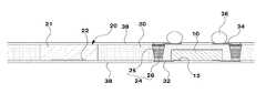
- FIGS. 3A to 3HThe manufacturing process for a typical wafer level fan-out package, which is a type of chip scale package will be described with reference to the attached drawings FIGS. 3A to 3H .
- individual chips ( 10 ) separated from a waferare attached to an adhesive surface such as a tape or a carrier at a lower surface thereof with predetermined intervals.
- an adhesive surfacesuch as a tape or a carrier
- a surface on which a boding pad was providedis attached to the adhesive surface (as shown in FIG. 3A ).
- the bonding padcan function as an input/output pad for electric signal.
- the molding compound resin ( 30 ) encapsulating the individual chip ( 10 )is forcibly detached from the adhesive surface, the lower surface on which the bonding pad is provided of the individual chips may be externally exposed. Then, in order to make lower and upper surfaces of the molding compound resin ( 30 ) as smooth as possible, a grinding process is utilized followed by a cleaning process on the lower surface of the chip.
- a lower redistribution layer ( 32 )which is a kind of metal distribution layer, may be formed from a bonding pad ( 12 ) of the individual chip ( 10 ) to a desired position on the lower surface of the molding compound resin ( 30 ), as shown in FIG. 3C .
- a metal redistribution layeris provided. Accordingly, the metal redistribution layer extends from the bonding pad to the outside so as to allow the input/output terminals to be attached to the bonding pad while maintaining a wider gap there between.
- a passivation layeris typically formed at a surface of the chip everywhere except where the bonding pad is located.
- a redistribution layeris formed utilizing a plating process.
- an insulating passivation layeris formed on the redistribution layer in order to prevent moisture and other foreign substances from permeating into the redistribution layer and to prevent electrical shorts between the redistribution layers.
- a through mold via ( 24 )may be formed at the molding compound resin ( 30 ) by using laser processing, as shown in FIGS. 3D and 3E .
- a plurality of through mold vias ( 24 )may be formed at certain positions around the chips ( 10 ) with equal intervals.
- the through mold via ( 24 )may be formed by performing the steps: forming a via hole ( 26 ) from the upper surface of the molding compound resin ( 30 ) to the lower surface on which the lower redistribution layer ( 32 ) is provided, using laser processing, as shown in FIG. 3D .
- Foreign substancesare then removed from an inner circumferential surface and surroundings of the via hole ( 26 ), followed by plating or filling of the lower redistribution layer 32 and a conductive metal ( 28 ), such as a metal paste, in the via hole ( 26 ) as shown in FIG. 3E .
- an upper redistribution layer ( 34 )may be formed from an upper end of the through via hole ( 22 ) to a desired position on an upper surface of the molding compound resin ( 30 ) similarly to the formation of the lower redistribution layer ( 32 ), and as shown in FIG. 3F .
- input/output terminal ( 36 )such as a solder ball, may be heated to melting state thereby coupling it to a ball pad, that is, a distal end of the upper redistribution layer ( 34 ) extending to a desired position on the upper surface of the molding compound resin ( 30 ), as illustrated in FIG. 3G .
- the laser drilling for forming a via hole from the upper surface of the molding compound resin to the lower surface thereofcan be performed in a state that an edge portion of the semiconductor chip may be recognized as a standard coordinate by using the X-ray examination.
- an error by a micro meter at the array spacing between the individual semiconductor chipsmay occur in the process of attaching the plurality of semiconductor chips to the adhesive surface with predetermined intervals.
- the process of forming the lower redistribution layeris in progress, it may be slightly out of position. Consequently, it is difficult to accurately form the via hole from a certain position on the surface of the molding compound resin, corresponding to the individual semiconductor chips and its surroundings, to the lower redistribution layer using laser processing.
- aspects of the present inventionsolve the above-mentioned problems, and provide a semiconductor device and a method of manufacturing the same, which can form a via hole from a surface of the molding compound resin to a lower redistribution layer around the individual semiconductor chips at an accurate location and an accurate interval, utilizing a fiducial die on a wafer at a position adjacent to the semiconductor chip, which enables the laser drilling means to recognize a fiducial pattern of the fiducial die as a standard coordinate while performing the laser drilling, when a plurality semiconductor chips are attached an adhesive surface with predetermined intervals.
- a semiconductor devicecomprising: a fiducial die being disposed at a predetermined position adjacent to a semiconductor chip sawed after being subjected to the wafer sawing process; a molding compound resin for encapsulating and guarding the semiconductor chip and the fiducial die in such a manner that an upper surface of the fiducial die can be exposed to the outside; a lower redistribution layer extending from a bonding pad of the individual semiconductor chip to a desired position at a lower surface of the molding compound resin; a through mold via including a via hole and a conductive metal material to be filled in the via hole, the via hole being formed from an upper surface of the molding compound resin to the lower surface of the molding compound resin on which the redistribution layer is provided by using laser drilling such that a laser drilling means can recognize the fiducial die as a standard coordinate; an upper redistribution layer extending from an upper end of the through mold via of a mold interposer to a desired position on an upper surface
- the fiducial diemay comprise a transparent member having a thickness larger than the thickness of the semiconductor device, and a fiducial pattern formed at a lower surface of the transparent member.
- the transparent member of the fiducial diemay comprise glass materials and the fiducial pattern may comprise the same material as the lower redistribution layer while performing the process of forming the lower redistribution layer.
- a method of manufacturing a semiconductor devicecomprising the steps of: attaching a plurality of semiconductors to an adhesive surface with predetermined intervals and simultaneously attaching a fiducial die having a thickness larger than the thickness of the semiconductor device to the adhesive surface at a position adjacent to the semiconductor device; molding the individual semiconductor chip and the fiducial die together by means of a molding compound resin; grinding an upper surface of the molding compound resin so as to expose an upper surface of the fiducial die to the outside; forming a lower redistribution layer from a bonding pad of the individual semiconductor chip to a desired position on a lower surface of the molding compound resin after forcibly detaching the molding compound resin encapsulating the semiconductor chip and the fiducial die from the adhesive surface; forming a via hole from the upper surface of the molding compound resin to the lower surface of the molding compound resin on which the redistribution layer is provided by performing laser drilling such that the laser drilling means may recognize the fiducial die as a standard coordinate; completing
- the fiducial diemay be provided with a fiducial pattern for allowing the laser drilling means to recognize it as a standard coordinate with the aid of a transparent member of the fiducial die when the fiducial die is attached to the adhesive surface together with the semiconductor device, in which the fiducial pattern is pre-formed on a lower surface of the transparent member.
- a fiducial patternmay be formed at a lower surface of a transparent member of the fiducial die when the redistribution layer is formed from the bonding pad of the semiconductor chip to a desired position of the molding compound resin, in which the fiducial pattern is made of the same material as the lower redistribution layer.
- the fiducial diewhen a Wafer Level Fan-Out Package is produced, the fiducial die may be formed on an adhesive surface at a predetermined location adjacent to a semiconductor chip, which is capable of allowing the laser drilling means to recognize the fiducial pattern of the fiducial die as a standard coordinate while performing the laser drilling. Accordingly, it is possible to form a via hole at an accurate position and an accurate interval, wherein the via hole may be formed from a surface of the molding compound resin to the lower redistribution layer disposed at a location adjacent to the individual semiconductor chip, by using the laser drilling.
- the fiducial patternmay be formed at the fiducial die by using the same material as the lower redistribution layer. Furthermore, the spacing between the fiducial pattern and the lower redistribution layer remains constant. As a result, the laser drilling means may accurately recognize the fiducial pattern as a standard coordinate and thereby result in the formation of the via hole at an accurate location.
- the present inventionprovides a Wafer Level Fan-Out Package, which is capable of forming a via hole of a through mold via at an accurate location by a laser drilling, even though a minute interval error may be present between a plurality of semiconductor chips or a lower redistribution layer is out of its position, resulting in a minor positioning error.
- the reference numeral “ 20 ”denotes a fiducial die according to the first exemplary embodiment, which is disposed at a position adjacent to a semiconductor chip ( 10 ) sawed after being subjected to the wafer sawing process.
- the fiducial die ( 20 )according to the first exemplary embodiment comprises a transparent member ( 21 ) having a thickness larger than the thickness of the semiconductor device ( 10 ), and a fiducial pattern ( 22 ) embedded in or attached to a lower surface of the transparent member ( 21 ).
- the fiducial pattern ( 22 )comprises a thin metal film and the transparent member ( 21 ) comprises glass.
- the fiducial die ( 20 )may comprise the transparent member ( 21 ) and the fiducial pattern ( 22 ) provided on the lower surface of the transparent member ( 21 ).
- the transparent member ( 21 )comprises glass, it allows a worker to view the laser drilling means passing through the transparent member ( 21 ).
- the fiducial pattern ( 22 )makes it possible for the laser drilling means to accurately recognize standard coordinates.
- a plurality of semiconductor chips ( 10 )may be attached on an adhesive surface ( 14 ) such as a tape or a carrier with predetermined intervals, as shown in FIG. 1A .
- an adhesive surfacesuch as a tape or a carrier with predetermined intervals, as shown in FIG. 1A .
- a surface having a bonding padthat is to say, an input/output pad for an electrical signal formed thereon may be attached to the adhesive surface.
- the fiducial die ( 20 ) having the fiducial pattern ( 22 ) formed at the lower surface of the transparent member ( 21 )may be attached to the adhesive surface ( 14 ) at a position away from the semiconductor chip ( 10 ) at a predetermined distance.
- the thickness of the fiducial die ( 20 )is greater than the thickness of the individual semiconductor device ( 10 ). Accordingly, when the fiducial die ( 20 ) is attached to the adhesive surface ( 14 ) together with the individual semiconductor device ( 10 ), the height of the fiducial die ( 20 ) is greater than the height of the individual semiconductor device ( 10 ).
- the individual semiconductor chip ( 10 ) and the fiducial die ( 20 )may be molded together utilizing a molding compound resin ( 30 ) so that upper and side surfaces of the individual semiconductor chip ( 10 ), and upper and side surfaces of the fiducial die ( 20 ) are encapsulated and guarded by the molding compound resin ( 30 ), as illustrated in FIG. 1B .
- the fiducial die ( 20 )may not directly contact an inner surface of the mold so as to prevent it from being damaged. As a result, the fiducial die ( 20 ) may be encapsulated and guarded by the molding compound resin.
- the upper surface of the molding compound resin ( 30 )may be ground down so as to externally expose the upper surface of the fiducial die ( 20 ).
- the fiducial die ( 20 )may be encapsulated and guarded by the molding compound resin of the semiconductor resin ( 10 ), as illustrated in FIG. 1C .
- the molding compound resin ( 30 ) encapsulating the semiconductor chip ( 10 ) and the fiducial die ( 20 )is detached from the adhesive surface ( 14 ), the lower surface of the semiconductor chip, which has the bonding pad ( 12 ) provided thereon, may be exposed to the outside. Thereafter, the lower redistribution layer ( 32 ) from the bonding pad ( 12 ) of the individual semiconductor chip ( 10 ) to a desired position on the lower surface of the molding compound resin ( 30 ) may be formed using a typical plating process, as illustrated in FIG. 1C .
- the reference numeral “ 38 ”denotes a passivation layer for preventing moisture and foreign substances, etc. from permeating into the redistribution layer ( 32 ) and for preventing an electrical short between the redistribution layers.
- the passivation layer ( 38 )comprises an insulating material.
- a via hole ( 26 ) from the upper surface of the molding compound resin ( 30 ) to the lower a lower surface of the molding compound resin ( 30 )may be formed at which the lower redistribution layer ( 32 ) using laser drilling, as illustrated in FIG. 1D .
- the laser drilling meansmay recognize the fiducial pattern ( 22 ) of the fiducial die ( 20 ) as a standard coordinate with the aid of the transparent member ( 21 ) of the fiducial die ( 20 ). Accordingly, it is possible to form the via hole ( 26 ) at an accurate position, which is formed from the upper surface to the lower surface of the molding compound resin ( 30 ).
- a conductive metal material ( 28 )may be filled in the via hole ( 26 ), resulting in the formation of the through mold via ( 24 ) in the molding compound resin ( 30 ).
- an upper redistribution layer ( 34 )may be formed extending from an upper end of the through mold via ( 24 ) to a desired position at an upper surface of the molding compound resin ( 30 ) utilizing a similar process as used in the formation of the lower redistribution layer ( 32 ). Then, an input/output terminal ( 36 ) may be heated to a melting state and coupled to a ball pad of the upper redistribution layer ( 34 ), which may be exposed to the outside via the passivation layer ( 38 ), at a distal end of the upper redistribution layer ( 34 ), as illustrated in FIG. 1E .
- the structuremay be sawn along a sawing line, that is, a boundary line between the individual packages of the molding compound resin, resulting in the completion of the individual Wafer Level Fan-Out Packages.
- the via hole ( 26 )from the surface of the molding compound resin to the lower redistribution layer at an accurate location and an accurate interval by utilizing laser drilling, even though a minute interval error may occur between a plurality of semiconductor chips or a lower redistribution layer is out of its position, resulting in a minor positioning error.
- the reference numeral “ 20 ”denotes a fiducial die according to the second exemplary embodiment of the present invention, which is disposed at a position adjacent to a semiconductor chip ( 10 ) sawed after being subjected to the process of sawing the wafer.
- the fiducial die ( 20 )according to the second exemplary embodiment comprises a transparent member ( 21 ) having a thickness larger than the thickness of the semiconductor device ( 10 ), and a fiducial pattern ( 22 ) embedded in or attached to a lower surface of the transparent member ( 21 ) during the formation of the lower redistribution layer ( 32 ).
- the transparent member ( 21 )comprises glass.
- a plurality of semiconductor chips ( 10 )may be attached to the adhesive surface ( 14 ) such as a tape or a carrier with predetermined intervals.
- a surface having a bonding pad, that is to say, an input/output pad for an electrical signal formed thereonmay be attached to the adhesive surface.
- the fiducial die ( 20 ) having the fiducial pattern ( 22 ) formed at the lower surface of the transparent member ( 21 )may be attached to the adhesive surface ( 14 ) at a position away from the semiconductor chip ( 10 ) at a predetermined distance, as illustrated in FIG. 2A .
- the thickness of the fiducial die ( 20 )may be greater than the thickness of the individual semiconductor device ( 10 ). Accordingly, when the fiducial die ( 20 ) is attached to the adhesive surface ( 14 ) together with the individual semiconductor device ( 10 ), the height of the fiducial die ( 20 ) is greater than the height of the individual semiconductor device ( 10 ).
- the fiducial die ( 20 ) attached to the adhesive surface ( 14 )may be shown in FIGS. 2A and 2B with only the transparent member ( 21 ) without having the fiducial pattern ( 22 ).
- the individual semiconductor chip ( 10 ) and the fiducial die ( 20 )may be molded together by a molding compound resin ( 30 ) so that upper and side surfaces of the individual semiconductor chip ( 10 ), and upper and side surfaces of the fiducial die ( 20 ) are encapsulated and guarded by the molding compound resin ( 30 ), as illustrated in FIG. 2B .
- a process of grinding an upper surface of the molding compound resin ( 30 )may proceed so as to externally expose an upper surface of the fiducial die ( 20 ).
- the upper surface of the transparent member ( 21 )is substantially exposed to the outside, as illustrated in FIG. 2C .
- the molding compound resin ( 30 ) encapsulating the semiconductor chip ( 10 ) and the fiducial die ( 20 )may be detached from the adhesive surface ( 14 ) so that the lower surface of the semiconductor chip having the bonding pad ( 12 ) provided thereon is exposed to the outside. Then, the lower redistribution layer ( 32 ) may be formed from the bonding pad ( 12 ) of the individual semiconductor chip ( 10 ) to a desired position on the lower surface of the molding compound resin ( 30 ) using a plating process, with the resulting structure shown in FIG. 2C .
- the fiducial pattern ( 22 )may be formed on the lower surface of the transparent member ( 21 ) of the fiducial die ( 20 ) at the same time.
- the fiducial pattern ( 22 )may comprise the same materials as that used in the process of plating the lower redistribution layer ( 32 ).
- the reference numeral “ 38 ”denotes a passivation layer for preventing moisture and foreign substances, etc. from permeating into the redistribution layer and for preventing the electrical short from being occurred between the redistribution layers.
- the passivation layeris made of an insulating material.
- a via hole ( 26 )may be formed from the upper surface of the molding compound resin ( 30 ) to a lower surface of the molding compound resin ( 30 ) in which the lower redistribution layer ( 32 ) is provided, by using laser drilling, resulting in the structure illustrated in FIG. 2D .
- the via hole ( 26 )may then be formed such that the laser drilling means recognizes the fiducial pattern ( 22 ) of the fiducial die ( 20 ) as a standard coordinate with the aid of the transparent member ( 21 ) of the fiducial die ( 20 ). Accordingly, it is possible to form the via hole ( 26 ) at an accurate position, which may be formed from the upper surface to the lower surface of the molding compound resin ( 30 ).
- a conductive metal material ( 28 )may fill in the via hole ( 26 ), resulting in the formation of the through mold via ( 24 ) in the molding compound resin ( 30 ).
- an upper redistribution layer ( 34 )may be formed extending from an upper end of the through mold via ( 24 ) to a desired position at an upper surface of the molding compound resin ( 30 ) in a similar manner to the formation of the lower redistribution layer ( 32 ). Then, an input/output terminal ( 36 ) may be heated to a state of melting and coupled to a ball pad of the upper redistribution layer ( 34 ), which may be exposed to the outside via the passivation layer ( 38 ), at a distal end of the upper redistribution layer ( 34 ). The resulting structure is illustrated in FIG. 2E .
- a process of sawing the structure along a sawing linethat is, a boundary line between the individual packages of the molding compound resin, may be utilized to result in the completion of the individual Wafer Level Fan-Out Packages.
- a wafer level fan-out package with a fiducial diemay comprise a semiconductor die and a transparent fiducial die both encapsulated in a molding compound resin, passivation layers on an upper surface and a lower surface of the molding compound resin except where redistribution layers are formed on upper and lower surfaces of the molding compound resin; and a metal pattern on a lower surface of the transparent fiducial die that is visible through an exposed upper surface of the transparent fiducial die.
- the patternmay comprise a standard coordinate for forming a through mold via utilizing laser drilling.
- the through mold viamay extend from the upper surface to the lower surface of the molding compound resin for electrically coupling a redistribution layer on the upper surface of the molding compound resin to a redistribution layer on the bottom surface of the molding compound resin.
- the patternmay be embedded in the lower surface of the fiducial die.
- the patternmay be deposited on the lower surface of the fiducial die.
- the redistribution layer on the lower surface of the molding compound resinmay be electrically coupled to a bonding pad on the semiconductor die.
- An input/output terminalmay be formed on the redistribution layer on the upper surface of the molding compound resin.
- the input/output terminalmay comprise a solder bump.
- the transparent fiducial diemay be thicker than the semiconductor die.
- the transparent fiducial diemay comprise a glass material.
- the pattern on the lower surface of the transparent fiducial diemay comprise the same material as the redistribution layer on the on the bottom surface of the molding compound resin.
- the formed through mold viamay comprise a
Landscapes
- Engineering & Computer Science (AREA)
- Computer Hardware Design (AREA)
- Power Engineering (AREA)
- Microelectronics & Electronic Packaging (AREA)
- General Physics & Mathematics (AREA)
- Physics & Mathematics (AREA)
- Condensed Matter Physics & Semiconductors (AREA)
- Manufacturing & Machinery (AREA)
- General Engineering & Computer Science (AREA)
- Ceramic Engineering (AREA)
- Structures Or Materials For Encapsulating Or Coating Semiconductor Devices Or Solid State Devices (AREA)
- Production Of Multi-Layered Print Wiring Board (AREA)
- Arrangement Of Elements, Cooling, Sealing, Or The Like Of Lighting Devices (AREA)
Abstract
Description
- 10: semiconductor chip
- 12: bonding pad
- 14: adhesive surface
- 20: fiducial die
- 21: transparent member
- 22: fiducial pattern
- 24: through mold via
- 26: via hole
- 28: conductive metal material
- 30: molding compound resin
- 32: lower redistribution layer
- 34: upper redistribution layer
- 36: input/output terminal
- 38: passivation film
Claims (20)
Applications Claiming Priority (2)
| Application Number | Priority Date | Filing Date | Title |
|---|---|---|---|
| KR1020120104430AKR20140038116A (en) | 2012-09-20 | 2012-09-20 | Led lamp |
| KR10-2012-0104430 | 2012-09-20 |
Publications (2)
| Publication Number | Publication Date |
|---|---|
| US20140077366A1 US20140077366A1 (en) | 2014-03-20 |
| US8946883B2true US8946883B2 (en) | 2015-02-03 |
Family
ID=50273627
Family Applications (1)
| Application Number | Title | Priority Date | Filing Date |
|---|---|---|---|
| US13/963,384ActiveUS8946883B2 (en) | 2012-09-20 | 2013-08-09 | Wafer level fan-out package with a fiducial die |
Country Status (2)
| Country | Link |
|---|---|
| US (1) | US8946883B2 (en) |
| KR (1) | KR20140038116A (en) |
Cited By (7)
| Publication number | Priority date | Publication date | Assignee | Title |
|---|---|---|---|---|
| US9391043B2 (en) | 2012-11-20 | 2016-07-12 | Amkor Technology, Inc. | Semiconductor device and manufacturing method thereof |
| US9543242B1 (en) | 2013-01-29 | 2017-01-10 | Amkor Technology, Inc. | Semiconductor package and fabricating method thereof |
| US9704842B2 (en) | 2013-11-04 | 2017-07-11 | Amkor Technology, Inc. | Interposer, manufacturing method thereof, semiconductor package using the same, and method for fabricating the semiconductor package |
| US9721872B1 (en) | 2011-02-18 | 2017-08-01 | Amkor Technology, Inc. | Methods and structures for increasing the allowable die size in TMV packages |
| US9960328B2 (en) | 2016-09-06 | 2018-05-01 | Amkor Technology, Inc. | Semiconductor device and manufacturing method thereof |
| US20180190511A1 (en)* | 2017-01-03 | 2018-07-05 | Stmicroelectronics (Grenoble 2) Sas | Method for manufacturing a cover for an electronic package and electronic package comprising a cover |
| US10483408B2 (en) | 2017-01-03 | 2019-11-19 | Stmicroelectronics (Grenoble 2) Sas | Method for making a cover for an electronic package and electronic package comprising a cover |
Families Citing this family (13)
| Publication number | Priority date | Publication date | Assignee | Title |
|---|---|---|---|---|
| US9589900B2 (en) | 2014-02-27 | 2017-03-07 | Taiwan Semiconductor Manufacturing Company, Ltd. | Metal pad for laser marking |
| US9735129B2 (en)* | 2014-03-21 | 2017-08-15 | Taiwan Semiconductor Manufacturing Company, Ltd. | Semiconductor packages and methods of forming the same |
| US9318452B2 (en) | 2014-03-21 | 2016-04-19 | Taiwan Semiconductor Manufacturing Company, Ltd. | Semiconductor packages and methods of forming the same |
| US9666522B2 (en) | 2014-05-29 | 2017-05-30 | Taiwan Semiconductor Manufacturing Company, Ltd. | Alignment mark design for packages |
| US9824990B2 (en) | 2014-06-12 | 2017-11-21 | Taiwan Semiconductor Manufacturing Company, Ltd. | Pad design for reliability enhancement in packages |
| US9881857B2 (en) | 2014-06-12 | 2018-01-30 | Taiwan Semiconductor Manufacturing Company, Ltd. | Pad design for reliability enhancement in packages |
| US9543277B1 (en)* | 2015-08-20 | 2017-01-10 | Invensas Corporation | Wafer level packages with mechanically decoupled fan-in and fan-out areas |
| US9543224B1 (en)* | 2015-12-09 | 2017-01-10 | Intel IP Corporation | Hybrid exposure for semiconductor devices |
| US10672729B2 (en) | 2017-03-30 | 2020-06-02 | Taiwan Semiconductor Manufacturing Co., Ltd. | Package structure and method of forming package structure |
| CN109686668A (en)* | 2018-11-22 | 2019-04-26 | 珠海越亚半导体股份有限公司 | It is a kind of to bury core process preposition integrated circuit packaging method and encapsulating structure |
| CN110581079B (en)* | 2019-09-23 | 2021-09-03 | 合肥矽迈微电子科技有限公司 | Fan-out type chip packaging method and fan-out type chip packaging body |
| KR20240118910A (en)* | 2019-10-11 | 2024-08-05 | 어플라이드 머티어리얼스, 인코포레이티드 | Die system and method of comparing alignment vectors |
| TWI749860B (en)* | 2020-11-10 | 2021-12-11 | 菱生精密工業股份有限公司 | Chip packaging method |
Citations (20)
| Publication number | Priority date | Publication date | Assignee | Title |
|---|---|---|---|---|
| US5250843A (en) | 1991-03-27 | 1993-10-05 | Integrated System Assemblies Corp. | Multichip integrated circuit modules |
| US5353498A (en) | 1993-02-08 | 1994-10-11 | General Electric Company | Method for fabricating an integrated circuit module |
| US5841193A (en) | 1996-05-20 | 1998-11-24 | Epic Technologies, Inc. | Single chip modules, repairable multichip modules, and methods of fabrication thereof |
| JP2001118947A (en) | 1999-10-19 | 2001-04-27 | Nec Corp | Semiconductor device and method of manufacturing package therefor |
| US6486005B1 (en) | 2000-04-03 | 2002-11-26 | Hynix Semiconductor Inc. | Semiconductor package and method for fabricating the same |
| US6727576B2 (en) | 2001-10-31 | 2004-04-27 | Infineon Technologies Ag | Transfer wafer level packaging |
| US6838776B2 (en) | 2003-04-18 | 2005-01-04 | Freescale Semiconductor, Inc. | Circuit device with at least partial packaging and method for forming |
| US6845554B2 (en) | 2001-11-22 | 2005-01-25 | Infineon Technologies Ag | Method for connection of circuit units |
| US6905914B1 (en) | 2002-11-08 | 2005-06-14 | Amkor Technology, Inc. | Wafer level package and fabrication method |
| US6921975B2 (en) | 2003-04-18 | 2005-07-26 | Freescale Semiconductor, Inc. | Circuit device with at least partial packaging, exposed active surface and a voltage reference plane |
| US7015075B2 (en) | 2004-02-09 | 2006-03-21 | Freescale Semiconuctor, Inc. | Die encapsulation using a porous carrier |
| US20060192301A1 (en) | 2004-04-30 | 2006-08-31 | Leal George R | Semiconductor device with a protected active die region and method therefor |
| US20060231958A1 (en) | 2003-12-03 | 2006-10-19 | Advanced Chip Engineering Technology, Inc. | Fan out type wafer level package structure and method of the same |
| US20070059866A1 (en) | 2003-12-03 | 2007-03-15 | Advanced Chip Engineering Technology Inc. | Fan out type wafer level package structure and method of the same |
| US7202107B2 (en) | 2003-07-28 | 2007-04-10 | Infineon Technologies Ag | Method for producing a semiconductor component with a plastic housing and carrier plate for performing the method |
| US7238602B2 (en) | 2004-10-26 | 2007-07-03 | Advanced Chip Engineering Technology Inc. | Chip-size package structure and method of the same |
| US7326592B2 (en) | 2005-04-04 | 2008-02-05 | Infineon Technologies Ag | Stacked die package |
| US7405102B2 (en) | 2006-06-09 | 2008-07-29 | Freescale Semiconductor, Inc. | Methods and apparatus for thermal management in a multi-layer embedded chip structure |
| US20080182363A1 (en) | 2007-01-31 | 2008-07-31 | Freescale Semiconductor, Inc. | Method for forming a microelectronic assembly including encapsulating a die using a sacrificial layer |
| US7623733B2 (en) | 2002-08-09 | 2009-11-24 | Sharp Kabushiki Kaisha | Image combination device, image combination method, image combination program, and recording medium for combining images having at least partially same background |
- 2012
- 2012-09-20KRKR1020120104430Apatent/KR20140038116A/ennot_activeCeased
- 2013
- 2013-08-09USUS13/963,384patent/US8946883B2/enactiveActive
Patent Citations (34)
| Publication number | Priority date | Publication date | Assignee | Title |
|---|---|---|---|---|
| US5250843A (en) | 1991-03-27 | 1993-10-05 | Integrated System Assemblies Corp. | Multichip integrated circuit modules |
| US5353498A (en) | 1993-02-08 | 1994-10-11 | General Electric Company | Method for fabricating an integrated circuit module |
| US5497033A (en) | 1993-02-08 | 1996-03-05 | Martin Marietta Corporation | Embedded substrate for integrated circuit modules |
| US5841193A (en) | 1996-05-20 | 1998-11-24 | Epic Technologies, Inc. | Single chip modules, repairable multichip modules, and methods of fabrication thereof |
| US6159767A (en) | 1996-05-20 | 2000-12-12 | Epic Technologies, Inc. | Single chip modules, repairable multichip modules, and methods of fabrication thereof |
| JP2001118947A (en) | 1999-10-19 | 2001-04-27 | Nec Corp | Semiconductor device and method of manufacturing package therefor |
| US6486005B1 (en) | 2000-04-03 | 2002-11-26 | Hynix Semiconductor Inc. | Semiconductor package and method for fabricating the same |
| US6727576B2 (en) | 2001-10-31 | 2004-04-27 | Infineon Technologies Ag | Transfer wafer level packaging |
| US6845554B2 (en) | 2001-11-22 | 2005-01-25 | Infineon Technologies Ag | Method for connection of circuit units |
| US7623733B2 (en) | 2002-08-09 | 2009-11-24 | Sharp Kabushiki Kaisha | Image combination device, image combination method, image combination program, and recording medium for combining images having at least partially same background |
| US7192807B1 (en) | 2002-11-08 | 2007-03-20 | Amkor Technology, Inc. | Wafer level package and fabrication method |
| US6905914B1 (en) | 2002-11-08 | 2005-06-14 | Amkor Technology, Inc. | Wafer level package and fabrication method |
| US7420272B1 (en) | 2002-11-08 | 2008-09-02 | Amkor Technology, Inc. | Two-sided wafer escape package |
| US7247523B1 (en) | 2002-11-08 | 2007-07-24 | Amkor Technology, Inc. | Two-sided wafer escape package |
| US6838776B2 (en) | 2003-04-18 | 2005-01-04 | Freescale Semiconductor, Inc. | Circuit device with at least partial packaging and method for forming |
| US6921975B2 (en) | 2003-04-18 | 2005-07-26 | Freescale Semiconductor, Inc. | Circuit device with at least partial packaging, exposed active surface and a voltage reference plane |
| US20080142960A1 (en) | 2003-04-18 | 2008-06-19 | Freescale Semiconductor, Inc. | Circuit device with at least partial packaging and method for forming |
| US7361987B2 (en) | 2003-04-18 | 2008-04-22 | Freescale Semiconductor, Inc. | Circuit device with at least partial packaging and method for forming |
| US7202107B2 (en) | 2003-07-28 | 2007-04-10 | Infineon Technologies Ag | Method for producing a semiconductor component with a plastic housing and carrier plate for performing the method |
| US20070059866A1 (en) | 2003-12-03 | 2007-03-15 | Advanced Chip Engineering Technology Inc. | Fan out type wafer level package structure and method of the same |
| US7262081B2 (en) | 2003-12-03 | 2007-08-28 | Wen-Kun Yang | Fan out type wafer level package structure and method of the same |
| US20090051025A1 (en) | 2003-12-03 | 2009-02-26 | Advanced Chip Engineering Technology Inc. | Fan out type wafer level package structure and method of the same |
| US7196408B2 (en) | 2003-12-03 | 2007-03-27 | Wen-Kun Yang | Fan out type wafer level package structure and method of the same |
| US20080105967A1 (en) | 2003-12-03 | 2008-05-08 | Advanced Chip Engineering Technology Inc. | Fan out type wafer level package structure and method of the same |
| US7459781B2 (en)* | 2003-12-03 | 2008-12-02 | Wen-Kun Yang | Fan out type wafer level package structure and method of the same |
| US20060231958A1 (en) | 2003-12-03 | 2006-10-19 | Advanced Chip Engineering Technology, Inc. | Fan out type wafer level package structure and method of the same |
| US7015075B2 (en) | 2004-02-09 | 2006-03-21 | Freescale Semiconuctor, Inc. | Die encapsulation using a porous carrier |
| US20060192301A1 (en) | 2004-04-30 | 2006-08-31 | Leal George R | Semiconductor device with a protected active die region and method therefor |
| US7238602B2 (en) | 2004-10-26 | 2007-07-03 | Advanced Chip Engineering Technology Inc. | Chip-size package structure and method of the same |
| US7339279B2 (en) | 2004-10-26 | 2008-03-04 | Advanced Chip Engineering Technology Inc. | Chip-size package structure and method of the same |
| US20080128884A1 (en) | 2005-04-04 | 2008-06-05 | Torsten Meyer | Stacked Die Package |
| US7326592B2 (en) | 2005-04-04 | 2008-02-05 | Infineon Technologies Ag | Stacked die package |
| US7405102B2 (en) | 2006-06-09 | 2008-07-29 | Freescale Semiconductor, Inc. | Methods and apparatus for thermal management in a multi-layer embedded chip structure |
| US20080182363A1 (en) | 2007-01-31 | 2008-07-31 | Freescale Semiconductor, Inc. | Method for forming a microelectronic assembly including encapsulating a die using a sacrificial layer |
Non-Patent Citations (2)
| Title |
|---|
| CAD-CIM Requirements Article IMAPS. |
| CAD—CIM Requirements Article IMAPS. |
Cited By (23)
| Publication number | Priority date | Publication date | Assignee | Title |
|---|---|---|---|---|
| US9721872B1 (en) | 2011-02-18 | 2017-08-01 | Amkor Technology, Inc. | Methods and structures for increasing the allowable die size in TMV packages |
| US11488892B2 (en) | 2011-02-18 | 2022-11-01 | Amkor Technology Singapore Holding Pte. Ltd. | Methods and structures for increasing the allowable die size in TMV packages |
| US10347562B1 (en) | 2011-02-18 | 2019-07-09 | Amkor Technology, Inc. | Methods and structures for increasing the allowable die size in TMV packages |
| US10679952B2 (en) | 2012-11-20 | 2020-06-09 | Amkor Technology, Inc. | Semiconductor device having an encapsulated front side and interposer and manufacturing method thereof |
| US9728514B2 (en) | 2012-11-20 | 2017-08-08 | Amkor Technology, Inc. | Semiconductor device and manufacturing method thereof |
| US11527496B2 (en) | 2012-11-20 | 2022-12-13 | Amkor Technology Singapore Holding Pte. Ltd. | Semiconductor device comprising semiconductor die and interposer and manufacturing method thereof |
| US9391043B2 (en) | 2012-11-20 | 2016-07-12 | Amkor Technology, Inc. | Semiconductor device and manufacturing method thereof |
| US9543242B1 (en) | 2013-01-29 | 2017-01-10 | Amkor Technology, Inc. | Semiconductor package and fabricating method thereof |
| US9852976B2 (en) | 2013-01-29 | 2017-12-26 | Amkor Technology, Inc. | Semiconductor package and fabricating method thereof |
| US9704842B2 (en) | 2013-11-04 | 2017-07-11 | Amkor Technology, Inc. | Interposer, manufacturing method thereof, semiconductor package using the same, and method for fabricating the semiconductor package |
| US10943858B2 (en) | 2013-11-19 | 2021-03-09 | Amkor Technology Singapore Holding Pte. Ltd. | Semiconductor package and fabricating method thereof |
| US10192816B2 (en) | 2013-11-19 | 2019-01-29 | Amkor Technology, Inc. | Semiconductor package and fabricating method thereof |
| US11652038B2 (en) | 2013-11-19 | 2023-05-16 | Amkor Technology Singapore Holding Pte. Ltd. | Semiconductor package with front side and back side redistribution structures and fabricating method thereof |
| US12159823B2 (en) | 2013-11-19 | 2024-12-03 | Amkor Technology Singapore Holding Pte. Ltd. | Semiconductor package with front side and back side redistribution structures and fabricating method thereof |
| US10490716B2 (en) | 2016-09-06 | 2019-11-26 | Amkor Technology, Inc. | Semiconductor device with optically-transmissive layer and manufacturing method thereof |
| US10784422B2 (en) | 2016-09-06 | 2020-09-22 | Amkor Technology, Inc. | Semiconductor device with optically-transmissive layer and manufacturing method thereof |
| US11437552B2 (en) | 2016-09-06 | 2022-09-06 | Amkor Technology Singapore Holding Pte. Ltd. | Semiconductor device with transmissive layer and manufacturing method thereof |
| US9960328B2 (en) | 2016-09-06 | 2018-05-01 | Amkor Technology, Inc. | Semiconductor device and manufacturing method thereof |
| US11942581B2 (en) | 2016-09-06 | 2024-03-26 | Amkor Technology Singapore Holding Pte. Ltd. | Semiconductor device with transmissive layer and manufacturing method thereof |
| US10483408B2 (en) | 2017-01-03 | 2019-11-19 | Stmicroelectronics (Grenoble 2) Sas | Method for making a cover for an electronic package and electronic package comprising a cover |
| US10833208B2 (en) | 2017-01-03 | 2020-11-10 | Stmicroelectronics (Grenoble 2) Sas | Method for manufacturing a cover for an electronic package and electronic package comprising a cover |
| US20180190511A1 (en)* | 2017-01-03 | 2018-07-05 | Stmicroelectronics (Grenoble 2) Sas | Method for manufacturing a cover for an electronic package and electronic package comprising a cover |
| US11688815B2 (en) | 2017-01-03 | 2023-06-27 | Stmicroelectronics (Grenoble 2) Sas | Method for manufacturing a cover for an electronic package and electronic package comprising a cover |
Also Published As
| Publication number | Publication date |
|---|---|
| US20140077366A1 (en) | 2014-03-20 |
| KR20140038116A (en) | 2014-03-28 |
Similar Documents
| Publication | Publication Date | Title |
|---|---|---|
| US8946883B2 (en) | Wafer level fan-out package with a fiducial die | |
| US11107701B2 (en) | Stiffener package and method of fabricating stiffener package | |
| US11152312B2 (en) | Packages with interposers and methods for forming the same | |
| US20200051944A1 (en) | Semiconductor device and manufacturing method thereof | |
| US20190189552A1 (en) | Semiconductor package and fabricating method thereof | |
| US9653445B2 (en) | Semiconductor device and method of fabricating 3D package with short cycle time and high yield | |
| KR20240125867A (en) | Semiconductor package and fabricating method thereof | |
| KR101579673B1 (en) | Method for fabricating semiconductor package and semiconductor package using the same | |
| KR101690371B1 (en) | Integrated fan-out package structures with recesses in molding compound | |
| TWI761342B (en) | Semiconductor package and fabricating method thereof | |
| KR101548426B1 (en) | Alignment in the packaging of integrated circuits | |
| US20170294409A1 (en) | Multi-Chip Fan Out Package and Methods of Forming the Same | |
| US9911718B2 (en) | ‘RDL-First’ packaged microelectronic device for a package-on-package device | |
| KR101151258B1 (en) | Semiconductor package and method for manufacturing the same | |
| KR101494814B1 (en) | Semiconductor package using glass and method for manufacturing the same | |
| US20120181562A1 (en) | Package having a light-emitting element and method of fabricating the same | |
| KR20070076846A (en) | Wafer level package having resin seal and manufacturing method thereof | |
| KR101478508B1 (en) | Wafer level fan out package and method for manufacturing the same | |
| US20170186711A1 (en) | Structure and method of fan-out stacked packages | |
| US20140377886A1 (en) | Method of manufacturing semiconductor device including grinding semiconductor wafer | |
| TW201807771A (en) | Chip package array and chip package | |
| US8283780B2 (en) | Surface mount semiconductor device | |
| KR101504899B1 (en) | Fan out semiconductor package and method for manufacturing the same | |
| CN106129031B (en) | Chip packaging structure and packaging method thereof | |
| KR20150120177A (en) | Manufacturing method of semiconductor device and semiconductor device thereof |
Legal Events
| Date | Code | Title | Description |
|---|---|---|---|
| AS | Assignment | Owner name:AMKOR TECHNOLOGY, INC., ARIZONA Free format text:ASSIGNMENT OF ASSIGNORS INTEREST;ASSIGNORS:KIM, SUNG KYU;KIM, JIN YOUNG;KIM, YOON JOO;AND OTHERS;SIGNING DATES FROM 20130731 TO 20130805;REEL/FRAME:031051/0287 | |
| STCF | Information on status: patent grant | Free format text:PATENTED CASE | |
| AS | Assignment | Owner name:BANK OF AMERICA, N.A., TEXAS Free format text:PATENT SECURITY AGREEMENT;ASSIGNOR:AMKOR TECHNOLOGY, INC.;REEL/FRAME:035613/0592 Effective date:20150409 | |
| AS | Assignment | Owner name:BANK OF AMERICA, N.A., AS AGENT, CALIFORNIA Free format text:SECURITY INTEREST;ASSIGNOR:AMKOR TECHNOLOGY, INC.;REEL/FRAME:046683/0139 Effective date:20180713 | |
| MAFP | Maintenance fee payment | Free format text:PAYMENT OF MAINTENANCE FEE, 4TH YEAR, LARGE ENTITY (ORIGINAL EVENT CODE: M1551) Year of fee payment:4 | |
| AS | Assignment | Owner name:AMKOR TECHNOLOGY SINGAPORE HOLDING PTE.LTD., SINGAPORE Free format text:ASSIGNMENT OF ASSIGNORS INTEREST;ASSIGNOR:AMKOR TECHNOLOGY, INC.;REEL/FRAME:054046/0673 Effective date:20191119 | |
| MAFP | Maintenance fee payment | Free format text:PAYMENT OF MAINTENANCE FEE, 8TH YEAR, LARGE ENTITY (ORIGINAL EVENT CODE: M1552); ENTITY STATUS OF PATENT OWNER: LARGE ENTITY Year of fee payment:8 |