US8946046B1 - Guided path for forming a conductive filament in RRAM - Google Patents
Guided path for forming a conductive filament in RRAMDownload PDFInfo
- Publication number
- US8946046B1 US8946046B1US13/462,653US201213462653AUS8946046B1US 8946046 B1US8946046 B1US 8946046B1US 201213462653 AUS201213462653 AUS 201213462653AUS 8946046 B1US8946046 B1US 8946046B1
- Authority
- US
- United States
- Prior art keywords
- resistive switching
- electrode
- forming
- region
- overlying
- Prior art date
- Legal status (The legal status is an assumption and is not a legal conclusion. Google has not performed a legal analysis and makes no representation as to the accuracy of the status listed.)
- Active
Links
- 239000000463materialSubstances0.000claimsabstractdescription177
- 238000000034methodMethods0.000claimsabstractdescription87
- 239000000758substrateSubstances0.000claimsabstractdescription20
- 238000005137deposition processMethods0.000claimsabstractdescription11
- 239000003989dielectric materialSubstances0.000claimsdescription58
- 229910021417amorphous siliconInorganic materials0.000claimsdescription32
- 239000007769metal materialSubstances0.000claimsdescription29
- 239000002210silicon-based materialSubstances0.000claimsdescription29
- 239000004065semiconductorSubstances0.000claimsdescription20
- 230000005684electric fieldEffects0.000claimsdescription17
- 229910052751metalInorganic materials0.000claimsdescription16
- 239000002184metalSubstances0.000claimsdescription16
- BQCADISMDOOEFD-UHFFFAOYSA-NSilverChemical compound[Ag]BQCADISMDOOEFD-UHFFFAOYSA-N0.000claimsdescription15
- 229910052709silverInorganic materials0.000claimsdescription15
- 239000004332silverSubstances0.000claimsdescription15
- KDLHZDBZIXYQEI-UHFFFAOYSA-NPalladiumChemical compound[Pd]KDLHZDBZIXYQEI-UHFFFAOYSA-N0.000claimsdescription14
- BASFCYQUMIYNBI-UHFFFAOYSA-NplatinumChemical compound[Pt]BASFCYQUMIYNBI-UHFFFAOYSA-N0.000claimsdescription14
- PXHVJJICTQNCMI-UHFFFAOYSA-NNickelChemical compound[Ni]PXHVJJICTQNCMI-UHFFFAOYSA-N0.000claimsdescription12
- 230000008021depositionEffects0.000claimsdescription12
- 230000015572biosynthetic processEffects0.000claimsdescription10
- RYGMFSIKBFXOCR-UHFFFAOYSA-NCopperChemical compound[Cu]RYGMFSIKBFXOCR-UHFFFAOYSA-N0.000claimsdescription8
- 229910052782aluminiumInorganic materials0.000claimsdescription8
- XAGFODPZIPBFFR-UHFFFAOYSA-NaluminiumChemical compound[Al]XAGFODPZIPBFFR-UHFFFAOYSA-N0.000claimsdescription8
- 229910052802copperInorganic materials0.000claimsdescription8
- 239000010949copperSubstances0.000claimsdescription8
- 230000004888barrier functionEffects0.000claimsdescription7
- 229910052763palladiumInorganic materials0.000claimsdescription7
- 229910052697platinumInorganic materials0.000claimsdescription7
- HCHKCACWOHOZIP-UHFFFAOYSA-NZincChemical compound[Zn]HCHKCACWOHOZIP-UHFFFAOYSA-N0.000claimsdescription6
- PCHJSUWPFVWCPO-UHFFFAOYSA-NgoldChemical compound[Au]PCHJSUWPFVWCPO-UHFFFAOYSA-N0.000claimsdescription6
- 229910052737goldInorganic materials0.000claimsdescription6
- 239000010931goldSubstances0.000claimsdescription6
- 229910052759nickelInorganic materials0.000claimsdescription6
- 229910052725zincInorganic materials0.000claimsdescription6
- 239000011701zincSubstances0.000claimsdescription6
- 230000007547defectEffects0.000claimsdescription5
- 238000004519manufacturing processMethods0.000claimsdescription5
- 230000008569processEffects0.000description25
- 230000015654memoryEffects0.000description18
- 239000007772electrode materialSubstances0.000description17
- VYPSYNLAJGMNEJ-UHFFFAOYSA-NSilicium dioxideChemical compoundO=[Si]=OVYPSYNLAJGMNEJ-UHFFFAOYSA-N0.000description10
- 238000000151depositionMethods0.000description10
- 229910052814silicon oxideInorganic materials0.000description10
- 238000005229chemical vapour depositionMethods0.000description9
- 238000009792diffusion processMethods0.000description9
- 239000002245particleSubstances0.000description7
- 229910052581Si3N4Inorganic materials0.000description6
- XUIMIQQOPSSXEZ-UHFFFAOYSA-NSiliconChemical compound[Si]XUIMIQQOPSSXEZ-UHFFFAOYSA-N0.000description6
- 230000008859changeEffects0.000description6
- 238000005240physical vapour depositionMethods0.000description6
- 229910052710siliconInorganic materials0.000description6
- 239000010703siliconSubstances0.000description6
- HQVNEWCFYHHQES-UHFFFAOYSA-Nsilicon nitrideChemical compoundN12[Si]34N5[Si]62N3[Si]51N64HQVNEWCFYHHQES-UHFFFAOYSA-N0.000description6
- 238000000231atomic layer depositionMethods0.000description4
- 238000010586diagramMethods0.000description4
- 230000007246mechanismEffects0.000description4
- 150000004767nitridesChemical class0.000description4
- 230000000694effectsEffects0.000description3
- 239000011521glassSubstances0.000description3
- 230000003993interactionEffects0.000description3
- 229910021420polycrystalline siliconInorganic materials0.000description3
- 239000000126substanceSubstances0.000description3
- 229910052721tungstenInorganic materials0.000description3
- 239000010937tungstenSubstances0.000description3
- XKRFYHLGVUSROY-UHFFFAOYSA-NArgonChemical compound[Ar]XKRFYHLGVUSROY-UHFFFAOYSA-N0.000description2
- 208000031481Pathologic ConstrictionDiseases0.000description2
- 229910000577Silicon-germaniumInorganic materials0.000description2
- LEVVHYCKPQWKOP-UHFFFAOYSA-N[Si].[Ge]Chemical compound[Si].[Ge]LEVVHYCKPQWKOP-UHFFFAOYSA-N0.000description2
- 239000011149active materialSubstances0.000description2
- 230000015556catabolic processEffects0.000description2
- 239000011248coating agentSubstances0.000description2
- 238000000576coating methodMethods0.000description2
- 239000004020conductorSubstances0.000description2
- 238000009713electroplatingMethods0.000description2
- 239000012212insulatorSubstances0.000description2
- 230000010354integrationEffects0.000description2
- 238000004518low pressure chemical vapour depositionMethods0.000description2
- 238000001000micrographMethods0.000description2
- 229910021421monocrystalline siliconInorganic materials0.000description2
- 239000012811non-conductive materialSubstances0.000description2
- 238000000623plasma-assisted chemical vapour depositionMethods0.000description2
- 238000003860storageMethods0.000description2
- WFKWXMTUELFFGS-UHFFFAOYSA-NtungstenChemical compound[W]WFKWXMTUELFFGS-UHFFFAOYSA-N0.000description2
- RTAQQCXQSZGOHL-UHFFFAOYSA-NTitaniumChemical compound[Ti]RTAQQCXQSZGOHL-UHFFFAOYSA-N0.000description1
- NRTOMJZYCJJWKI-UHFFFAOYSA-NTitanium nitrideChemical compound[Ti]#NNRTOMJZYCJJWKI-UHFFFAOYSA-N0.000description1
- 239000000956alloySubstances0.000description1
- 229910052786argonInorganic materials0.000description1
- 238000001311chemical methods and processMethods0.000description1
- 238000007796conventional methodMethods0.000description1
- 238000013500data storageMethods0.000description1
- 238000006731degradation reactionMethods0.000description1
- 238000004070electrodepositionMethods0.000description1
- 238000007772electroless platingMethods0.000description1
- 230000005669field effectEffects0.000description1
- 238000010438heat treatmentMethods0.000description1
- 230000014759maintenance of locationEffects0.000description1
- 238000010297mechanical methods and processMethods0.000description1
- 230000005226mechanical processes and functionsEffects0.000description1
- 230000005055memory storageEffects0.000description1
- 239000002923metal particleSubstances0.000description1
- 238000012986modificationMethods0.000description1
- 230000004048modificationEffects0.000description1
- 238000007517polishing processMethods0.000description1
- 230000005855radiationEffects0.000description1
- MZLGASXMSKOWSE-UHFFFAOYSA-Ntantalum nitrideChemical compound[Ta]#NMZLGASXMSKOWSE-UHFFFAOYSA-N0.000description1
- 239000010936titaniumSubstances0.000description1
- 229910052719titaniumInorganic materials0.000description1
- -1tungsten nitrideChemical class0.000description1
Images


Classifications
- H—ELECTRICITY
- H10—SEMICONDUCTOR DEVICES; ELECTRIC SOLID-STATE DEVICES NOT OTHERWISE PROVIDED FOR
- H10N—ELECTRIC SOLID-STATE DEVICES NOT OTHERWISE PROVIDED FOR
- H10N70/00—Solid-state devices having no potential barriers, and specially adapted for rectifying, amplifying, oscillating or switching
- H10N70/20—Multistable switching devices, e.g. memristors
- H10N70/231—Multistable switching devices, e.g. memristors based on solid-state phase change, e.g. between amorphous and crystalline phases, Ovshinsky effect
- H—ELECTRICITY
- H01—ELECTRIC ELEMENTS
- H01L—SEMICONDUCTOR DEVICES NOT COVERED BY CLASS H10
- H01L21/00—Processes or apparatus adapted for the manufacture or treatment of semiconductor or solid state devices or of parts thereof
- H01L21/02—Manufacture or treatment of semiconductor devices or of parts thereof
- H01L21/04—Manufacture or treatment of semiconductor devices or of parts thereof the devices having potential barriers, e.g. a PN junction, depletion layer or carrier concentration layer
- H01L21/34—Manufacture or treatment of semiconductor devices or of parts thereof the devices having potential barriers, e.g. a PN junction, depletion layer or carrier concentration layer the devices having semiconductor bodies not provided for in groups H01L21/18, H10D48/04 and H10D48/07, with or without impurities, e.g. doping materials
- H01L21/46—Treatment of semiconductor bodies using processes or apparatus not provided for in groups H01L21/428
- H01L21/461—Treatment of semiconductor bodies using processes or apparatus not provided for in groups H01L21/428 to change their surface-physical characteristics or shape, e.g. etching, polishing, cutting
- H01L21/4763—Deposition of non-insulating, e.g. conductive -, resistive -, layers on insulating layers; After-treatment of these layers
- H01L45/04—
- H—ELECTRICITY
- H10—SEMICONDUCTOR DEVICES; ELECTRIC SOLID-STATE DEVICES NOT OTHERWISE PROVIDED FOR
- H10N—ELECTRIC SOLID-STATE DEVICES NOT OTHERWISE PROVIDED FOR
- H10N70/00—Solid-state devices having no potential barriers, and specially adapted for rectifying, amplifying, oscillating or switching
- H10N70/20—Multistable switching devices, e.g. memristors
- H10N70/24—Multistable switching devices, e.g. memristors based on migration or redistribution of ionic species, e.g. anions, vacancies
- H10N70/245—Multistable switching devices, e.g. memristors based on migration or redistribution of ionic species, e.g. anions, vacancies the species being metal cations, e.g. programmable metallization cells
- H—ELECTRICITY
- H10—SEMICONDUCTOR DEVICES; ELECTRIC SOLID-STATE DEVICES NOT OTHERWISE PROVIDED FOR
- H10N—ELECTRIC SOLID-STATE DEVICES NOT OTHERWISE PROVIDED FOR
- H10N70/00—Solid-state devices having no potential barriers, and specially adapted for rectifying, amplifying, oscillating or switching
- H10N70/801—Constructional details of multistable switching devices
- H10N70/821—Device geometry
- H10N70/826—Device geometry adapted for essentially vertical current flow, e.g. sandwich or pillar type devices
- H—ELECTRICITY
- H10—SEMICONDUCTOR DEVICES; ELECTRIC SOLID-STATE DEVICES NOT OTHERWISE PROVIDED FOR
- H10N—ELECTRIC SOLID-STATE DEVICES NOT OTHERWISE PROVIDED FOR
- H10N70/00—Solid-state devices having no potential barriers, and specially adapted for rectifying, amplifying, oscillating or switching
- H10N70/801—Constructional details of multistable switching devices
- H10N70/841—Electrodes
- H10N70/8416—Electrodes adapted for supplying ionic species
- H—ELECTRICITY
- H10—SEMICONDUCTOR DEVICES; ELECTRIC SOLID-STATE DEVICES NOT OTHERWISE PROVIDED FOR
- H10N—ELECTRIC SOLID-STATE DEVICES NOT OTHERWISE PROVIDED FOR
- H10N70/00—Solid-state devices having no potential barriers, and specially adapted for rectifying, amplifying, oscillating or switching
- H10N70/801—Constructional details of multistable switching devices
- H10N70/881—Switching materials
- H10N70/884—Switching materials based on at least one element of group IIIA, IVA or VA, e.g. elemental or compound semiconductors
- H—ELECTRICITY
- H10—SEMICONDUCTOR DEVICES; ELECTRIC SOLID-STATE DEVICES NOT OTHERWISE PROVIDED FOR
- H10N—ELECTRIC SOLID-STATE DEVICES NOT OTHERWISE PROVIDED FOR
- H10N70/00—Solid-state devices having no potential barriers, and specially adapted for rectifying, amplifying, oscillating or switching
- H10N70/011—Manufacture or treatment of multistable switching devices
- H10N70/061—Shaping switching materials
- H10N70/063—Shaping switching materials by etching of pre-deposited switching material layers, e.g. lithography
- H—ELECTRICITY
- H10—SEMICONDUCTOR DEVICES; ELECTRIC SOLID-STATE DEVICES NOT OTHERWISE PROVIDED FOR
- H10N—ELECTRIC SOLID-STATE DEVICES NOT OTHERWISE PROVIDED FOR
- H10N70/00—Solid-state devices having no potential barriers, and specially adapted for rectifying, amplifying, oscillating or switching
- H10N70/011—Manufacture or treatment of multistable switching devices
- H10N70/061—Shaping switching materials
- H10N70/066—Shaping switching materials by filling of openings, e.g. damascene method
Definitions
- the present inventionis related to switching devices. More particularly, the present invention provides a device structure and a method to form a resistive switching device having an improved switching performance. Embodiments of the present invention have been applied to a non-volatile memory device. But it should be recognized that the present invention can have a much broader range of applicability.
- the inventor of the present inventionhas recognized the success of semiconductor devices has been mainly driven by an intensive transistor down-scaling process.
- FETsfield effect transistors
- physical problemssuch as short channel effect begin to hinder proper device operation.
- FETsfield effect transistors
- Flash memoriesother performance degradations or problems may occur as device sizes shrink.
- a high voltageis usually required for programming of such memories, however, as device sizes shrink, the high programming voltage can result in dielectric breakdown and other problems. Similar problems can occur with other types of non-volatile memory devices other than Flash memories.
- RAMnon-volatile random access memory
- Fe RAMferroelectric RAM
- MRAMmagneto-resistive RAM
- ORAMorganic RAM
- PCRAMphase change RAM
- a common drawback with these memory devicesinclude that they often require new materials that are incompatible with typical CMOS manufacturing.
- Organic RAM or ORAMrequires organic chemicals that are currently incompatible with large volume silicon-based fabrication techniques and foundries.
- Fe-RAM and MRAM devicestypically require materials using a high temperature anneal step, and thus such devices cannot be normally be incorporated with large volume silicon-based fabrication techniques.
- Additional drawbacks with these devicesinclude that such memory cells often lack one or more key attributes required of non-volatile memories.
- Fe-RAM and MRAM devicestypically have fast switching (e.g. “0” to “1”) characteristics and good programming endurance, however, such memory cells are difficult to scale to small sizes.
- switching of PCRAM devicestypically includes Joules heating and undesirably require high power consumption.
- the present inventionis related to switching devices. More particularly, the present invention provides a device structure and a method to form a resistive switching device having an improved switching performance. Embodiments of the present invention have been applied to a non-volatile memory device. But it should be recognized that the present invention can have a much broader range of applicability.
- a method of forming a resistive switching device for a non-volatile memory deviceincludes providing a substrate having a surface region, forming a first dielectric material overlying the surface region of the substrate, and forming a first electrode structure in a portion of the first dielectric material.
- a processincludes forming a second dielectric material overlying the first electrode, forming an opening structure in a portion of the second dielectric material to expose a surface region of the first electrode structure, the opening structure being characterized by an aspect ratio, and forming a resistive switching material overlying the second dielectric material and filling at least a portion of the opening structure using a deposition process, the resistive switching material having a surface region characterized by a planar region and an indent structure, the indent structure overlying the first electrode structure.
- a methodincludes maintaining a first thickness of resistive switching material between the planar region and the first electrode structure, maintaining a second thickness of resistive switching material between the indent structure and the first electrode structure, wherein the first thickness is larger than the second thickness, and forming a second electrode structure overlying the resistive switching material including the indent structure.
- a resistive switching devicefor a non-volatile memory device.
- a devicemay include a first electrode, and a resistive switching material configured in an opening region in a dielectric material overlying the first electrode, the resistive switching material being characterized by a surface region having a planar region and an indent structure, at least a portion of the planar region being configured overlying the first electrode while maintaining a first thickness of resistive switching material relative to the first electrode, the indent structure being configured overlying the first electrode while maintaining a second thickness of resistive switching material relative to the first electrode, wherein the first thickness exceeds the second thickness.
- An apparatusmay include a second electrode overlying the resistive switching material including the indent structure.
- a resistive switching deviceis formed according to a method.
- One techniqueincludes providing a substrate having a surface region, forming a first dielectric material overlying the surface region of the substrate, and forming a first electrode in a portion of the first dielectric material.
- a processincludes forming a second dielectric material overlying the first electrode, forming an opening structure in a portion of the second dielectric material to expose a surface region of the first electrode structure, the opening structure being characterized by an aspect ratio, and forming a resistive switching material overlying the second dielectric material and filling at least a portion of the opening structure using a deposition process, the resistive switching material having a surface region characterized by a planar region and an indent structure, the indent structure overlying the first electrode structure.
- a methodmay include maintaining a first thickness of resistive switching material between the planar region and the first electrode structure, maintaining a second thickness of resistive switching material between the indent structure and the first electrode structure, wherein the first thickness is larger than the second thickness, and forming a second electrode structure overlying the resistive switching material including the indent structure.
- a method of forming a resistive switching device for a non-volatile memory deviceincludes providing a substrate having a surface region and forming a first dielectric material overlying the surface region of the substrate.
- the methodincludes forming a first electrode structure overlying the first dielectric material and forming a resistive switching material structure overlying the first electrode.
- the resistive switching material structureincludes a vertical side wall region.
- the methodforms a second dielectric material overlying the resistive switching material structure including the side wall region and forms a first material derived from the resistive switching material and the second dielectric material in a first material region in a vicinity of the side wall region.
- a second electrode structureis formed overlying the resistive switching material structure including the first material region.
- a resistive switching devicefor a non-volatile memory device.
- the deviceincludes a first electrode structure, a resistive switching material structure overlying the first electrode.
- the resistive switching material structureincludes a resistive switching material having a vertical side wall region.
- a dielectric materialoverlies the resistive switching material structure including the vertical side wall region.
- the deviceincludes a first material region comprising a first material configured in a vicinity of the vertical side wall region.
- the first materialis formed and derived from the dielectric material and the resistive switching material.
- a second electrodeis configured overlying the resistive switching material structure and the first material region.
- the first material regionprovides a path and facilitates formation of a conductive structure derived from the second electrode upon application of a programming voltage.
- embodiments according to the present inventionprovide various methods and device structures to form a conductive filament structure in a resistive switching device to change a resistance state or bit value of the device.
- the deviceis characterized by a low operating voltage (for example, low programming voltage) and a well defined region to form the conductive filament structure for a robust fabrication method.
- various devices according to the present inventioncan be characterized by a good endurance, reliable and fast switching among others.
- the present devicecan have programmed to more than one resistive state for a multibit device.
- the present device disposed in a crossbar configurationcan be vertically integrated to form a high density memory device thus drastically reduce cost per bit, a major attribute for present and future application in consumer devices.
- the present devicecan be implemented in a vast variety of applications such as date storage, code storage, embedded devices, for example, as configuration bit for field programmable gate array, radiation hardened application, and others.
- the present devicecan be configured to be write once read many times, write many times read once, or fully re-writable. Depending on the application, one or more of these benefits can be achieved.
- FIGS. 1 and 2are simplified diagram illustrating a conventional resistive switching device and its operation
- FIGS. 3-13are simplified diagrams illustrating a method of forming a resistive switching device for a non-volatile memory device according to various embodiments of the present invention.
- FIGS. 14-21are simplified diagrams illustrating an alternative method of forming a resistive switching device for a non-volatile memory device according to various embodiments of the present invention.
- FIG. 22is a scanning electron microscope image of an amorphous silicon material surface structure formed according to various embodiment of the present invention.
- the present inventionis related to switching devices. More particularly, the present invention provides a device structure and a method to form a resistive switching device having an improved switching performance. Embodiments of the present invention have been applied to a non-volatile memory device. But it should be recognized that the present invention can have a much broader range of applicability.
- Resistive switching deviceis a two terminal device having a resistive switching material configured in an intersection region of a first electrode and a second electrode.
- the switching mechanism or state change mechanismcan be based on a filament structure derived from a conductive material formed in the amorphous silicon material upon application of an electric field.
- the conductive materialcan be derived from, for example, the second electrode. The formation of the conductive structure and its interaction with the amorphous silicon material as well as its interaction with the first electrode would affect the switching characteristic thus the performance of the device.
- switching voltageis usually quite low (no greater than about 6 or 7 volts).
- Embodiments according to the presentprovide a method and a device structure for a well defined path or preferred path for the formation of the filament structure.
- FIG. 1is a simplified diagram illustrating a conventional switching device structure 100 .
- the convention switching deviceincludes a first electrode 102 , a second electrode 104 , and a switching material 106 sandwiched between first electrode 102 and second electrode 104 .
- Second electrode 104can have a portion that includes a metal material.
- the metal materialcan be silver, platinum, palladium, or other suitable metal materials having a suitable diffusivity characteristic in the amorphous silicon material.
- a metal region 108is formed in switching material 106 and in contact with the top electrode. The metal region is formed largely by a diffusion mechanism, assisted by an electric field resulting from the first voltage 112 .
- FIG. 2illustrates growth of metal region 108 in switching material 106 for the conventional resistive switching device.
- the diffusion of the metal material from second electrode 104 into the switching materialis assisted by first voltage 112 and sometimes results in a continuous metal region.
- first voltage 112As metal region 108 grows, an end region of metal region 108 becomes sharper and closer to the bottom electrode. Once the end region is sharp enough and close enough to the bottom electrode, the electric field would have a much greater effect on the metal region growth than diffusion.
- a filament structure 202is formed by hopping of a metal particle from a defect site to the next defect site in the amorphous silicon material upon application of a suitable voltage.
- filament structure 202is due to the presence of the electric filed and aided by diffusion in contrast to the metal region growth.
- Metal region 108 including filament structure 202form a conductive path for the resistive switching device.
- diffusion of materialcan be uncontrollable, it is desirable that the formation of metal region especially filament structure 202 can be in a predetermined path controlled substantially by applied electric field.
- FIGS. 3-13illustrate a method for forming a resistive switching device according to various embodiments of the present invention.
- a substrate 302 having a surface region 304is provided.
- the substratecan be a semiconductor material such as monocrystalline silicon, silicon on insulator (SOI), silicon germanium, and polycrystalline silicon, and others.
- the substratecan further include one or more transistor device formed thereon.
- the one or more transistor devicecan be controlling circuitry for the resistive switching device.
- the semiconductor substrate 302can have one or more MOS devices formed thereon.
- the one or more MOS devicescan be controlling circuitry for the resistive memory devices in specific embodiments.
- the one or more MOS devicesmay include other functionality, such as a processor, logic, or the like.
- a processor, or the likemay include resistive memory memories as described herein. Because the state-change memories are relatively non-volatile, the states of devices, such as processors, or the like may be maintained while power is not supplied to the processors. To a user, such capability would greatly enhance the power-on power-off performance of devices including such processors. Additionally, such capability would greatly reduce the power consumption of devices including such processors. In particular, because such memories are non-volatile, the processor need not draw power to refresh the memory states, as is common with CMOS type memories. Accordingly, embodiments of the present invention are directed towards processors or other logic incorporating these memory devices, as described herein, devices (e.g. smart phones, network devices) incorporating such memory devices, and the like.
- devicese.g. smart phones, network devices
- First dielectric material 402can be silicon oxide, silicon nitride, silicon oxynitride, a high K dielectric, a low K dielectric, or a dielectric stack having alternating layer of silicon oxide and silicon nitride (for example an ONO stack), including any combination of these, and others.
- First dielectric material 402can be deposited using techniques such as chemical vapor deposition, including low pressure chemical vapor deposition, plasma enhanced chemical vapor deposition, high density plasma chemical vapor deposition, atomic layer deposition (ALD), physical vapor deposition, spin on coating, including any combination of these, and others.
- First electrode material 502can be a suitable metal material including alloy materials, or a semiconductor material having a suitable conductivity characteristic.
- the metal materialcan be tungsten, aluminum, copper or silver, and others. These metal materials may be deposited using a physical vapor deposition process, chemical vapor deposition process, electroplating, or electroless deposition process, including any combinations of these, and others.
- the semiconductor materialcan be, for example, a suitably doped silicon material in certain embodiments.
- first electrode material 502can include one or more adhesion material or diffusion material to prevent the metal material to contaminate portions of the device in certain embodiments. Diffusion barrier material or adhesion material may each include titanium, titanium nitride, tungsten nitride, tantalum nitride, and others.
- the semiconductor materialcan be a doped poly-silicon material depending on the implementation.
- first electrode material 502subjects first electrode material 502 to a first pattern and etch process to form a plurality of first electrode structure(s) 602 overlying first dielectric material 402 .
- first electrode structure 602is spatially configured to extend in a first direction (e.g. in and out of the page).
- Second dielectric material 702is deposited overlying the plurality of first electrode structure 602 to isolate each of the plurality of first electrode structure 602 .
- Second dielectric material 702can include silicon oxide, silicon nitride, silicon oxynitride, a high K dielectric, a low K dielectric, or a dielectric stack having alternating layer of silicon oxide and silicon nitride (for example an ONO stack), including any combination of these, and others.
- Second dielectric material 702can be deposited using techniques such as chemical vapor deposition, including low pressure chemical vapor deposition, plasma enhanced chemical vapor deposition, high density plasma chemical vapor deposition, atomic layer deposition (ALD), physical vapor deposition, spin on coating, including any combination of these, and others.
- chemical vapor depositionincluding low pressure chemical vapor deposition, plasma enhanced chemical vapor deposition, high density plasma chemical vapor deposition, atomic layer deposition (ALD), physical vapor deposition, spin on coating, including any combination of these, and others.
- Second dielectric material 702is subjected to a planarizing process to form a substantially planarized surface region 802 and maintaining a thickness 804 of second dielectric material 702 overlying first electrode structure(s) 602 .
- the planarizing processcan be a chemical/mechanical process, an etch back process, a combination thereof, and others. Alternatively, the planarizing process can remove a portion of second dielectric material 702 to expose a surface region of first electrode structure 602 and a thickness 804 of second dielectric material can then be deposited overlying the exposed surface region of the first electrode structure 602 .
- an opening structure 902is formed in portions of the second dielectric material 702 to expose a surface region 904 of first electrode structure 602 .
- First opening structurecan be a trench structure configured substantially parallel to the first direction of the first electrode stricture(s) 602 in various embodiments. Opening structure 902 is characterized by an aspect ratio (ratio of height (up and down on the page) to width (left and right on the page).
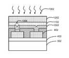
- the methodincludes forming a resistive switching material 1002 overlying the second dielectric material and to fill opening structure 902 .
- Resistive switching materialcan be a non-conductive material characterized by an electric resistance depending on an electric field present in the resistive switching material.
- the resistive switching materialcan be an amorphous silicon material having an intrinsic semiconductor characteristic or intrinsic amorphous silicon material. The intrinsic semiconductor characteristic is maintained by not intentionally doping the amorphous silicon material during deposition or after deposition.
- the intrinsic amorphous silicon material 1002may be deposited using a conformal deposition process to form a surface region 1004 having a planar region and an indent structure 1006 .
- the conformal depositioncan be a chemical vapor deposition process that provides a good step coverage for the resistive switching material.
- the indent structureis characterized by a width and a depth that can be determined by the deposition process parameters (for example, deposition rate, deposition temperature, and others) as well as the aspect ratio of the opening structure 902 .
- indent structure 1006has a tapered structure directed towards first electrode structure 602 and a thickness 1008 of resistive switching material 1002 is maintained between indent structure 1006 and first electrode structure 602 .
- thickness 1008is thinner than a thickness 1010 between the planar region of surface region 1004 and first electrode structure 602 .
- thickness 1008is thinner than thickness 1010 , when an electric field is applied across the resistive switching material 1002 , a metallic filament, as described herein is preferentially formed within the region of indent structure 1006 .
- a scanning electron microscope image 2200 of an amorphous silicon material surfaceis illustrated in FIG. 22 .
- the amorphous silicon materialis formed by steps as illustrated in FIGS. 3-10 .
- Dark regions as reference by numeral 2202are the indent structures.
- the methodincludes forming a second electrode material 1102 overlying resistive switching material 1002 filling indent structure 1006 , as shown.
- second electrode material 1102may be silver, gold, palladium, platinum, copper, aluminum, nickel, zinc, and others.
- Second electrode material 1102is selected to have a suitable diffusion characteristic in resistive switching material 1002 in a presence of an electric field. The electric field in a vicinity of the tapered structure 1006 is enhanced thus providing a path for a conductive filament to form in the resistive switching material 1002 upon application of the electric field.
- the conductive filamentcomprises a plurality of conductive particles derived from the second electrode material.
- the pathcan be a drift path or a diffusion path for the plurality of conductive particles upon application of the electric field.
- the electric fieldis enhanced, in the vicinity of the tapered region, threshold voltage required to form the conductive filament is reduced. Additionally, device dimension can be further scaled down as the conductive filament is defined.
- the silver material or the second electrode material 1102is in direct contact with the amorphous silicon 1002 used as the resistive switching material in a specific embodiment.
- a thin layer of materiale.g. oxide, nitride, is formed prior to the deposition of the silver material on top of the amorphous silicon used as the resistive switching material. This interposing thin layer of material may be naturally or specifically grown or formed.
- one or more etch operationse.g. HF etch, Argon etch
- the thickness of the materiale.g.
- oxideprior to deposition of the silver material may range from about 20 angstroms to about 50 angstroms; in other embodiments, the thickness may range from about 30 angstroms to about 40 angstroms; or the like.
- an additional layer of amorphous siliconmay be disposed upon the top of the thin layer of (oxide, nitride, barrier) material, prior to deposition of the silver material. This additional layer of amorphous silicon (not intentionally doped) may be used to help bind the silver material to the thin layer of material (e.g. oxide, nitride, barrier). In some examples, the thickness may be on the order of 20-50 angstroms.
- the order of layersmay be: undoped amorphous silicon used as the resistive switching material, a thin layer of material (e.g. oxide, nitride, barrier), a thin layer of amorphous silicon, and the silver material.
- a thin layer of materiale.g. oxide, nitride, barrier
- the methodincludes forming a second wiring material 1202 overlying the second electrode material 1102 .
- Second wiring materialcan be selected from a metal material such as aluminum, copper, and tungsten. Second wiring material may also be a doped semiconductor material (n+ doped or p+ doped) having a suitable conductivity depending on the implementation.
- the methodincludes subjecting second wiring material 1202 to a third pattern and etch process 1302 to form a second wiring structure.
- the second wiring structureis spatially configured to extend in a second direction (e.g. left and right on the page) orthogonal to the first direction (e.g. in and out of the page) of first wiring structure 602 to form a crossbar structure for the resistive switching device.
- second wiring materialmay not be needed as second electrode material may provide for the second wiring material.
- second wiring material 1202 and second electrode material 1102may be concurrently subjected to the third pattern and etch process to form the second wiring structure.
- the second wiring structure and the first wiring structureprovide connection to a respective transistor on the substrate for operations such as select, read, write, and erase for the resistive switching device.
- an alternative method of forming a resistive switching device having a path for the formation of the conductive particlesis provided.
- the path for the formation of the conductive particlesis configured in a material region and configured as a preferred path for formation of a conductive filament structure to change the resistance of the resistive switching material in various embodiments.
- Partially formed resistive switching device 1400can be fabricated according to steps in FIGS. 2-7 .
- the methodincludes subjecting second dielectric material 702 to a planarization process to expose a surface region 1502 of first electrode 602 .
- the planarization processcan be a chemical mechanical polishing process or an etch back process, or a combination.
- the planarization processcan use the first electrode material as an etch stop.
- etch stop materialcan be implemented to maintain an integrity of first electrode surface 1502 .
- the alternative methodincludes forming a resistive switching material 1602 overlying exposed surface region 1502 of first electrode structure 602 and second dielectric material 702 , which has been planarized.
- Resistive switching material 1602can be a non-conductive material characterized by an electric resistance depending on an electric field present in the resistive switching material.
- resistive switching material 1602can be an amorphous silicon material having an intrinsic semiconductor characteristic or intrinsic amorphous silicon material hereafter. The intrinsic semiconductor characteristic is maintained by not intentionally doped the amorphous silicon material during deposition or after deposition, as discussed in detail, above.
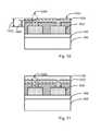
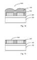
- the alternative methodincludes subjecting a resistive switching material to a pattern and etch process 1704 to form a resistive switching material structure 1702 .
- Resistive switching material structure 1702can be configured as a pillar stricture overlying the first electrode structure 602 and maintaining an electric and physical contact with first electrode structure 602 in various embodiments.
- Resistive switching material structure 1702includes a vertical wall region 1706 , as shown.
- the alternative methodforms a third dielectric material 1802 overlying resistive switching material structure 1702 including vertical side wall region 1706 .
- Third dielectric materialcan be a silicon oxide material deposited using a deposition process selected from a chemical vapor deposition process, a spin on glass (SOG), and a physical vapor deposition process including a combination thereof. Other suitable dielectric material may be used depending on the application.
- First material 1902is derived from an interaction of the resistive switching material (for example, the intrinsic amorphous silicon material) and the third dielectric material (for example, the silicon oxide material) in various embodiments.
- the resistive switching materialfor example, the intrinsic amorphous silicon material
- the third dielectric materialfor example, the silicon oxide material
- second electrode material 2002overlying at least resistive switching material structure 1702 and first material region 1902 as shown in FIG. 20 .
- second electrode material 2002can be an active metal material selected from silver, gold, palladium, platinum, copper, aluminum, nickel, zinc, and others.
- Second electrode material 2002may be deposited using techniques such as physical vapor deposition process, chemical vapor deposition process, electrochemical deposition (for example, electroplating, electroless plating, and others).
- second electrode material 2002is subjected to a pattern and etch process to form a second electrode structure 2102 , as shown in FIG. 21 .
- Second electrode structure 2102is configured to overlie resistive switching material structure 1702 as well as first material region 1902 in various embodiments.
- first material region 1902is configured as a path for an active metal material region to form when an electric field is applied.
- the electric fieldmay be a first voltage having a magnitude no less than a first threshold voltage applied to the second electrode.
- the first voltageis a positive voltage applied to the second electrode with respect to the first electrode in various embodiments.
- the active metal material 1702 regionincludes a filament structure comprising one or more active metal material particles.
- the filament structureis further characterized by a first distance between the one or more active material particles and a second distance between the filament structure and the first electrode.
- first electrode structure 602 , resistive switching material structure 1702 including first material region 1902 , and second electrode structure 2102form a resistive switching device 2104 for a non-volatile memory device in various embodiments.
- the filament structureIn a programming operation (for example upon application of a positive voltage to second electrode 2102 with respect to first electrode 602 ), the filament structure extends towards the first electrode structure and cause the resistive switching device to change from a high resistance state (bit value “0”) to a low resistance state (bit value 1).
- bit value “0”)high resistance state
- bit value 1low resistance state
- a negative voltage applied to second electrode 2102 in an erase operationwould cause the filament structure to retract and cause the resistive switching device to be in the high resistance state.
- the erase voltagecan have substantially a same amplitude as the programming voltage or can also be different depending on the implementation.
- the programming voltageis typically no greater than 8 volts and can range from about 2 volts to 6 volts depending on the device dimension, and others.
- Resistive switching device 2104is characterized by a good data retention (maintaining respective resistance states after removal of programming or erase voltage) and high endurance (ability to cycle).
- a method of forming a resistive switching device for a non-volatile memory devicecomprising:
- the resistive switching materialcomprising a vertical side wall region
- the substratecomprises a semiconductor material selected from monocrystalline silicon, silicon on insulator (SOI), silicon germanium, and polycrystalline silicon.
- the first dielectric materialis selected from: silicon oxide, silicon nitride, a dielectric stack of alternating layers of silicon oxide and silicon nitride (ONO), a high K dielectric material, a low K dielectric material, and a spin on glass material.
- resistive switching material structurecomprises an amorphous silicon material having an intrinsic semiconductor characteristic.
- the second dielectric materialcomprises a silicon oxide material deposited using a deposition process selected from a chemical vapor deposition process, a spin on glass (SOG), and a physical vapor deposition process and a combination thereof.
- the second electrode structurecomprises an active metal material selected from silver, gold, palladium, platinum, copper, aluminum, nickel, and zinc.
- the active metal material regioncomprises a filament structure, the filament structure comprising one or more active metal material particles.
- a resistive switching device for a non-volatile memory devicecomprising:
- a resistive switching material structurecomprising a resistive switching material having a vertical side wall region overlying the first electrode
- a first material regioncomprising a first material configured in a vicinity of the vertical side wall region, the first material being formed from the dielectric material and the resistive switching material;
- the first electrode structurecomprises a semiconductor material.
- the resistive switching materialcomprises an amorphous silicon material having an intrinsic semiconductor characteristic.
- the dielectric materialcomprises a silicon oxide material.
- the device of claim 36 wherein the second electrode structurecomprises an active metal material selected from silver, gold, palladium, platinum, copper, aluminum, nickel, and zinc.
- the active metal materialforms an active material region derived from the second electrode structure at least in the first material region upon application of a first positive voltage to the second electrode structure.
Landscapes
- Engineering & Computer Science (AREA)
- Physics & Mathematics (AREA)
- Condensed Matter Physics & Semiconductors (AREA)
- General Physics & Mathematics (AREA)
- Manufacturing & Machinery (AREA)
- Computer Hardware Design (AREA)
- Microelectronics & Electronic Packaging (AREA)
- Power Engineering (AREA)
- Semiconductor Memories (AREA)
Abstract
Description
Claims (20)
Priority Applications (4)
| Application Number | Priority Date | Filing Date | Title |
|---|---|---|---|
| US13/462,653US8946046B1 (en) | 2012-05-02 | 2012-05-02 | Guided path for forming a conductive filament in RRAM |
| US14/573,817US9972778B2 (en) | 2012-05-02 | 2014-12-17 | Guided path for forming a conductive filament in RRAM |
| US14/611,022US9601692B1 (en) | 2010-07-13 | 2015-01-30 | Hetero-switching layer in a RRAM device and method |
| US14/613,299US9570678B1 (en) | 2010-06-08 | 2015-02-03 | Resistive RAM with preferental filament formation region and methods |
Applications Claiming Priority (1)
| Application Number | Priority Date | Filing Date | Title |
|---|---|---|---|
| US13/462,653US8946046B1 (en) | 2012-05-02 | 2012-05-02 | Guided path for forming a conductive filament in RRAM |
Related Parent Applications (1)
| Application Number | Title | Priority Date | Filing Date |
|---|---|---|---|
| US14/611,022Continuation-In-PartUS9601692B1 (en) | 2010-06-08 | 2015-01-30 | Hetero-switching layer in a RRAM device and method |
Related Child Applications (2)
| Application Number | Title | Priority Date | Filing Date |
|---|---|---|---|
| US14/573,817DivisionUS9972778B2 (en) | 2010-07-13 | 2014-12-17 | Guided path for forming a conductive filament in RRAM |
| US14/613,299Continuation-In-PartUS9570678B1 (en) | 2010-06-08 | 2015-02-03 | Resistive RAM with preferental filament formation region and methods |
Publications (1)
| Publication Number | Publication Date |
|---|---|
| US8946046B1true US8946046B1 (en) | 2015-02-03 |
Family
ID=52395619
Family Applications (2)
| Application Number | Title | Priority Date | Filing Date |
|---|---|---|---|
| US13/462,653ActiveUS8946046B1 (en) | 2010-06-08 | 2012-05-02 | Guided path for forming a conductive filament in RRAM |
| US14/573,817ActiveUS9972778B2 (en) | 2010-07-13 | 2014-12-17 | Guided path for forming a conductive filament in RRAM |
Family Applications After (1)
| Application Number | Title | Priority Date | Filing Date |
|---|---|---|---|
| US14/573,817ActiveUS9972778B2 (en) | 2010-07-13 | 2014-12-17 | Guided path for forming a conductive filament in RRAM |
Country Status (1)
| Country | Link |
|---|---|
| US (2) | US8946046B1 (en) |
Cited By (4)
| Publication number | Priority date | Publication date | Assignee | Title |
|---|---|---|---|---|
| US10062845B1 (en)* | 2016-05-13 | 2018-08-28 | Crossbar, Inc. | Flatness of memory cell surfaces |
| US10522754B2 (en) | 2016-06-15 | 2019-12-31 | Crossbar, Inc. | Liner layer for dielectric block layer |
| US10749110B1 (en) | 2016-07-15 | 2020-08-18 | Crossbar, Inc. | Memory stack liner comprising dielectric block layer material |
| CN115148901A (en)* | 2021-03-31 | 2022-10-04 | 科洛斯巴股份有限公司 | Resistance switching memory with constrained filars and method therefor |
Families Citing this family (5)
| Publication number | Priority date | Publication date | Assignee | Title |
|---|---|---|---|---|
| US9653680B2 (en)* | 2015-06-27 | 2017-05-16 | Intel Corporation | Techniques for filament localization, edge effect reduction, and forming/switching voltage reduction in RRAM devices |
| WO2018063209A1 (en)* | 2016-09-29 | 2018-04-05 | Intel Corporation | Resistive random access memory cell |
| WO2018063287A1 (en)* | 2016-09-30 | 2018-04-05 | Intel Corporation | Conductive bridge resistive random access memory cell |
| WO2019200206A1 (en)* | 2018-04-12 | 2019-10-17 | The University Of Chicago | Silicon compatible tin-based cationic filamentary device |
| US11730070B2 (en) | 2019-02-27 | 2023-08-15 | International Business Machines Corporation | Resistive random-access memory device with step height difference |
Citations (235)
| Publication number | Priority date | Publication date | Assignee | Title |
|---|---|---|---|---|
| US680652A (en) | 1897-11-08 | 1901-08-13 | Leonard L Elden | Circuit-breaker. |
| US4433468A (en) | 1980-03-26 | 1984-02-28 | Nippon Electric Co., Ltd. | Method for making semiconductor device having improved thermal stress characteristics |
| US4684972A (en) | 1981-08-07 | 1987-08-04 | The British Petroleum Company, P.L.C. | Non-volatile amorphous semiconductor memory device utilizing a forming voltage |
| US4741601A (en) | 1984-10-08 | 1988-05-03 | Nec Corporation | Non-linear device for driving liquid crystal display |
| US5139911A (en) | 1989-01-04 | 1992-08-18 | Fuji Xerox Co., Ltd. | Electrophotographic photoreceptor with two part surface layer |
| US5242855A (en) | 1991-09-30 | 1993-09-07 | Nec Corporation | Method of fabricating a polycrystalline silicon film having a reduced resistivity |
| US5278085A (en) | 1992-08-11 | 1994-01-11 | Micron Semiconductor, Inc. | Single mask process for forming both n-type and p-type gates in a polycrystalline silicon layer during the formation of a semiconductor device |
| US5315131A (en) | 1990-11-22 | 1994-05-24 | Matsushita Electric Industrial Co., Ltd. | Electrically reprogrammable nonvolatile memory device |
| US5335219A (en) | 1991-01-18 | 1994-08-02 | Ovshinsky Stanford R | Homogeneous composition of microcrystalline semiconductor material, semiconductor devices and directly overwritable memory elements fabricated therefrom, and arrays fabricated from the memory elements |
| US5360981A (en) | 1989-05-11 | 1994-11-01 | British Telecommunications Public Limited Company | Amorphous silicon memory |
| US5457649A (en) | 1994-08-26 | 1995-10-10 | Microchip Technology, Inc. | Semiconductor memory device and write-once, read-only semiconductor memory array using amorphous-silicon and method therefor |
| US5538564A (en) | 1994-03-18 | 1996-07-23 | Regents Of The University Of California | Three dimensional amorphous silicon/microcrystalline silicon solar cells |
| US5541869A (en) | 1991-10-22 | 1996-07-30 | British Telecommunications, Plc | Resistive memory element |
| US5594363A (en) | 1995-04-07 | 1997-01-14 | Zycad Corporation | Logic cell and routing architecture in a field programmable gate array |
| US5614756A (en) | 1990-04-12 | 1997-03-25 | Actel Corporation | Metal-to-metal antifuse with conductive |
| US5645628A (en) | 1994-07-14 | 1997-07-08 | Matsushita Electric Industrial Co., Ltd. | Electroless plating bath used for forming a wiring of a semiconductor device, and method of forming a wiring of a semiconductor device |
| US5751012A (en) | 1995-06-07 | 1998-05-12 | Micron Technology, Inc. | Polysilicon pillar diode for use in a non-volatile memory cell |
| US5840608A (en) | 1996-11-22 | 1998-11-24 | United Microelectronics Corporation | High density ROM and a method of making the same |
| US5970332A (en) | 1995-03-28 | 1999-10-19 | U.S. Philips Corporation | Method of manufacturing a semiconductor device with a BiCMOS circuit |
| US5973335A (en) | 1994-12-22 | 1999-10-26 | U.S. Philips Corporation | Semiconductor memory devices with amorphous silicon alloy |
| US5998244A (en) | 1996-08-22 | 1999-12-07 | Micron Technology, Inc. | Memory cell incorporating a chalcogenide element and method of making same |
| US6122318A (en) | 1996-10-31 | 2000-09-19 | Kabushiki Kaisha Toshiba | Video encoding apparatus and video decoding apparatus |
| US6128214A (en) | 1999-03-29 | 2000-10-03 | Hewlett-Packard | Molecular wire crossbar memory |
| US6143642A (en) | 1997-12-22 | 2000-11-07 | Vlsi Technology, Inc. | Programmable semiconductor structures and methods for making the same |
| US6180998B1 (en) | 1998-03-30 | 2001-01-30 | Lsi Logic Corporation | DRAM with built-in noise protection |
| US6259116B1 (en) | 1997-10-22 | 2001-07-10 | U.S. Philips Corporation | Multiple memory element semiconductor memory devices |
| US6288435B1 (en) | 1999-12-28 | 2001-09-11 | Xerox Corporation | Continuous amorphous silicon layer sensors using doped poly-silicon back contact |
| US6291836B1 (en) | 1996-06-05 | 2001-09-18 | U. S. Philips Corporation | Method of operating a programmable, non-volatile memory device |
| US6436818B1 (en) | 1997-02-19 | 2002-08-20 | Micron Technology, Inc. | Semiconductor structure having a doped conductive layer |
| US6436765B1 (en) | 2001-02-09 | 2002-08-20 | United Microelectronics Corp. | Method of fabricating a trenched flash memory cell |
| US6492694B2 (en) | 1998-02-27 | 2002-12-10 | Micron Technology, Inc. | Highly conductive composite polysilicon gate for CMOS integrated circuits |
| WO2003034498A1 (en) | 2001-10-16 | 2003-04-24 | Midwest Research Institute | Stacked switchable element and diode combination |
| US20030141565A1 (en) | 2002-01-28 | 2003-07-31 | Fumihiko Hirose | Diode |
| US20030174574A1 (en) | 2002-03-12 | 2003-09-18 | Perner Frederick A. | Write pulse circuit for a magnetic memory |
| US6627530B2 (en) | 2000-12-22 | 2003-09-30 | Matrix Semiconductor, Inc. | Patterning three dimensional structures |
| US20030206659A1 (en) | 1998-09-08 | 2003-11-06 | Canon Kabushiki Kaisha | Image processing apparatus including an image data encoder having at least two scalability modes and method therefor |
| US20040026682A1 (en) | 2002-06-17 | 2004-02-12 | Hai Jiang | Nano-dot memory and fabricating same |
| US6762474B1 (en) | 1998-06-10 | 2004-07-13 | Agere Systems Inc. | Method and apparatus for temperature compensation of read-only memory |
| US6768157B2 (en) | 2001-08-13 | 2004-07-27 | Advanced Micro Devices, Inc. | Memory device |
| US20040170040A1 (en) | 2002-08-02 | 2004-09-02 | Unity Semiconductor Corporation | Rewritable memory with non-linear memory element |
| US20040202041A1 (en) | 2003-04-11 | 2004-10-14 | Sharp Kabushiki Kaisha | Memory cell, memory device and manufacturing method of memory cell |
| US6815286B2 (en) | 2001-08-13 | 2004-11-09 | Advanced Micro Devices, Inc. | Memory device |
| US6821879B2 (en) | 2002-10-30 | 2004-11-23 | Xerox Corporation | Copper interconnect by immersion/electroless plating in dual damascene process |
| US6838720B2 (en) | 2001-08-13 | 2005-01-04 | Advanced Micro Devices, Inc. | Memory device with active passive layers |
| US6848012B2 (en) | 2002-09-27 | 2005-01-25 | Broadcom Corporation | Method and system for an adaptive multimode media queue |
| US20050020510A1 (en) | 2002-08-29 | 2005-01-27 | Benedict Dale L. | D-mannose contraceptives |
| US20050029587A1 (en) | 1995-06-07 | 2005-02-10 | Harshfield Steven T. | Method and apparatus for forming an integrated circuit electrode having a reduced contact area |
| US6858481B2 (en) | 2001-08-13 | 2005-02-22 | Advanced Micro Devices, Inc. | Memory device with active and passive layers |
| US6858482B2 (en) | 2002-04-10 | 2005-02-22 | Micron Technology, Inc. | Method of manufacture of programmable switching circuits and memory cells employing a glass layer |
| US20050041498A1 (en) | 2003-06-16 | 2005-02-24 | Claudio Resta | Writing circuit for a phase change memory device |
| US6864127B2 (en) | 1997-04-25 | 2005-03-08 | Semiconductor Energy Laboratory Co., Ltd. | Semiconductor device and method of fabricating the same |
| US20050052915A1 (en) | 2002-12-19 | 2005-03-10 | Matrix Semiconductor, Inc. | Nonvolatile memory cell without a dielectric antifuse having high- and low-impedance states |
| US20050062045A1 (en) | 2002-10-02 | 2005-03-24 | Arup Bhattacharyya | Processes of forming stacked resistor constructions |
| US20050073881A1 (en) | 2003-10-06 | 2005-04-07 | Tran Lung The | Magnetic memory device including groups of series-connected memory elements |
| US6881994B2 (en) | 2000-08-14 | 2005-04-19 | Matrix Semiconductor, Inc. | Monolithic three dimensional array of charge storage devices containing a planarized surface |
| US20050101081A1 (en) | 2003-09-30 | 2005-05-12 | Kabushiki Kaisha Toshiba | Nonvolatile semiconductor memory and a fabrication method thereof |
| US6927430B2 (en) | 2001-06-28 | 2005-08-09 | Sharp Laboratories Of America, Inc. | Shared bit line cross-point memory array incorporating P/N junctions |
| US20050175099A1 (en) | 2004-02-06 | 2005-08-11 | Nokia Corporation | Transcoder and associated system, method and computer program product for low-complexity reduced resolution transcoding |
| US6939787B2 (en) | 1999-12-28 | 2005-09-06 | Fujitsu Limited | Method for fabricating semiconductor device having gate electrode with polymetal structure of polycrystalline silicon film and metal film |
| US6946719B2 (en) | 2003-12-03 | 2005-09-20 | Matrix Semiconductor, Inc | Semiconductor device including junction diode contacting contact-antifuse unit comprising silicide |
| US20060017488A1 (en) | 2004-07-21 | 2006-01-26 | Sharp Laboratories Of America, Inc. | Mono-polarity switchable PCMO resistor trimmer |
| US7020006B2 (en) | 2002-08-02 | 2006-03-28 | Unity Semiconductor Corporation | Discharge of conductive array lines in fast memory |
| US7023093B2 (en) | 2002-10-24 | 2006-04-04 | International Business Machines Corporation | Very low effective dielectric constant interconnect Structures and methods for fabricating the same |
| US20060134837A1 (en) | 1998-11-16 | 2006-06-22 | Vivek Subramanian | Vertically stacked field programmable nonvolatile memory and method of fabrication |
| US7102150B2 (en) | 2001-05-11 | 2006-09-05 | Harshfield Steven T | PCRAM memory cell and method of making same |
| US7122853B1 (en) | 2004-08-17 | 2006-10-17 | Fasl, Inc. | Method to improve yield and simplify operation of polymer memory cells |
| US20060246606A1 (en) | 2005-05-02 | 2006-11-02 | Sharp Laboratories Of America, Inc. | Self-aligned cross point resistor memory array |
| US20060281244A1 (en) | 2005-06-08 | 2006-12-14 | Masayuki Ichige | Nonvolatile semiconductor memory device and method of manufacturing the same |
| US20070008773A1 (en) | 2005-07-11 | 2007-01-11 | Matrix Semiconductor, Inc. | Nonvolatile memory cell comprising switchable resistor and transistor |
| US20070015348A1 (en) | 2005-07-18 | 2007-01-18 | Sharp Laboratories Of America, Inc. | Crosspoint resistor memory device with back-to-back Schottky diodes |
| US20070045615A1 (en) | 2005-08-31 | 2007-03-01 | Samsung Electronics Co., Ltd. | Non-volatile organic resistance random access memory device and method of manufacturing the same |
| US7187577B1 (en) | 2005-11-23 | 2007-03-06 | Grandis, Inc. | Method and system for providing current balanced writing for memory cells and magnetic devices |
| US20070087508A1 (en) | 2003-12-03 | 2007-04-19 | Herner S B | Method for making a p-i-n diode crystallized adjacent to a silicide in series with a dielectric antifuse |
| US20070090425A1 (en) | 2005-09-28 | 2007-04-26 | Matrix Semiconductor, Inc. | Memory cell comprising switchable semiconductor memory element with trimmable resistance |
| US20070091685A1 (en) | 2004-01-27 | 2007-04-26 | Guterman Daniel C | Efficient verification for coarse/fine programming of non-volatile memory |
| US20070105390A1 (en) | 2005-11-09 | 2007-05-10 | Oh Travis B | Oxygen depleted etching process |
| US20070105284A1 (en) | 2003-12-03 | 2007-05-10 | Herner S B | Method for forming a memory cell comprising a semiconductor junction diode crystallized adjacent to a silicide |
| US7221599B1 (en) | 2004-11-01 | 2007-05-22 | Spansion, Llc | Polymer memory cell operation |
| US7238607B2 (en) | 2002-12-19 | 2007-07-03 | Sandisk 3D Llc | Method to minimize formation of recess at surface planarized by chemical mechanical planarization |
| US20070205510A1 (en) | 2006-03-03 | 2007-09-06 | Lavoie Adrien R | Noble metal barrier layers |
| US20070228414A1 (en) | 2006-03-31 | 2007-10-04 | Sandisk 3D, Llc | Heterojunction device comprising a semiconductor and a resistivity-switching oxide or nitride |
| JP2007281208A (en) | 2006-04-07 | 2007-10-25 | Matsushita Electric Ind Co Ltd | Multilayer variable resistance element array, variable resistance device, multilayer nonvolatile memory element array, and nonvolatile memory device |
| US7289353B2 (en) | 2004-08-17 | 2007-10-30 | Spansion, Llc | Systems and methods for adjusting programming thresholds of polymer memory cells |
| US20070284575A1 (en) | 2005-07-18 | 2007-12-13 | Sharp Laboratories Of America, Inc. | Metal/semiconductor/metal current limiter |
| JP2007328857A (en) | 2006-06-07 | 2007-12-20 | Sony Corp | Storage device |
| US20070290186A1 (en) | 2006-05-04 | 2007-12-20 | El Mostafa Bourim | Non-volatile variable resistance memory device and method of fabricating the same |
| US20070295950A1 (en) | 2006-06-27 | 2007-12-27 | Samsung Electronics Co., Ltd. | Variable resistance random access memory device and a method of fabricating the same |
| US20070297501A1 (en) | 2006-06-08 | 2007-12-27 | Via Technologies, Inc. | Decoding Systems and Methods in Computational Core of Programmable Graphics Processing Unit |
| US20080002481A1 (en) | 2002-12-20 | 2008-01-03 | Dietmar Gogl | Integrated Circuit, Method of Operating an Integrated Circuit, Method of Manufacturing an Integrated Circuit, Memory Module, Stackable Memory Module |
| US20080006907A1 (en) | 2006-07-06 | 2008-01-10 | Samsung Electronics Co., Ltd | Non-volatile memory device including a variable resistance material |
| US7324363B2 (en) | 2005-12-12 | 2008-01-29 | Synopsys, Inc. | SPICE optimized for arrays |
| US20080048164A1 (en) | 2006-07-11 | 2008-02-28 | Matsushita Electric Industrial Co., Ltd. | Electro-resistance element, method of manufacturing the same and electro-resistance memory using the same |
| US20080089110A1 (en) | 2006-10-16 | 2008-04-17 | Warren Robinett | Crossbar-memory systems and methods for writing to and reading from crossbar memory junctions of crossbar-memory systems |
| US20080090337A1 (en) | 2006-10-03 | 2008-04-17 | Williams R Stanley | Electrically actuated switch |
| US7365411B2 (en) | 2004-08-12 | 2008-04-29 | Micron Technology, Inc. | Resistance variable memory with temperature tolerant materials |
| US20080106926A1 (en) | 2006-11-08 | 2008-05-08 | Symetrix Corporation | Non-volatile resistance switching memories and methods of making same |
| US20080106925A1 (en) | 2006-11-08 | 2008-05-08 | Symetrix Corporation | Correlated electron memory |
| US7405418B2 (en) | 2004-02-17 | 2008-07-29 | Infineon Technologies Ag | Memory device electrode with a surface structure |
| US20080185567A1 (en) | 2007-02-05 | 2008-08-07 | Nitin Kumar | Methods for forming resistive switching memory elements |
| US20080198934A1 (en) | 2007-02-20 | 2008-08-21 | Edward Hong | Motion refinement engine for use in video encoding in accordance with a plurality of sub-pixel resolutions and methods for use therewith |
| US20080205179A1 (en) | 2007-02-28 | 2008-08-28 | Qimonda Ag | Integrated circuit having a memory array |
| US20080206931A1 (en) | 2002-07-26 | 2008-08-28 | Laurent Breuil | Nonvolatile memory element and production method thereof and storage memory arrangement |
| US20080220601A1 (en) | 2007-03-05 | 2008-09-11 | Nitin Kumar | Methods for forming nonvolatile memory elements with resistive-switching metal oxides |
| US20080232160A1 (en) | 2007-02-27 | 2008-09-25 | International Business Machines Corporation | Rectifying element for a crosspoint based memory array architecture |
| US20080278990A1 (en) | 2007-05-09 | 2008-11-13 | Pragati Kumar | Resistive-switching nonvolatile memory elements |
| US20080304312A1 (en) | 2007-06-11 | 2008-12-11 | Macronix International Co., Ltd. | Resistance memory with tungsten compound and manufacturing |
| US20080311722A1 (en) | 2007-06-15 | 2008-12-18 | Sandisk 3D Llc | Method for forming polycrystalline thin film bipolar transistors |
| US20090001345A1 (en) | 2007-06-29 | 2009-01-01 | April Schricker | Memory cell that employs a selectively deposited reversible resistance-switching element and methods of forming the same |
| US20090003717A1 (en) | 2007-06-28 | 2009-01-01 | Mitsubishi Electric Corporation | Image encoding device, image decoding device, image encoding method and image decoding method |
| US7474000B2 (en) | 2003-12-05 | 2009-01-06 | Sandisk 3D Llc | High density contact to relaxed geometry layers |
| WO2009005699A1 (en) | 2007-06-29 | 2009-01-08 | Sandisk 3D, Llc | Memory cell that employs a selectively grown reversible resistance-switching element and methods of forming the same |
| US20090014707A1 (en) | 2006-10-20 | 2009-01-15 | Wei Lu | Non-volatile solid state resistive switching devices |
| US20090052226A1 (en) | 2007-08-24 | 2009-02-26 | Samsung Electronics Co., Ltd | Resistive random access memory device |
| US7499355B2 (en) | 2006-07-31 | 2009-03-03 | Sandisk 3D Llc | High bandwidth one time field-programmable memory |
| US20090095951A1 (en) | 2007-10-12 | 2009-04-16 | Ovonyx, Inc. | Memory Device With Low Reset Current |
| US7521705B2 (en) | 2005-08-15 | 2009-04-21 | Micron Technology, Inc. | Reproducible resistance variable insulating memory devices having a shaped bottom electrode |
| US7534625B2 (en) | 2004-09-24 | 2009-05-19 | Karpov Ilya V | Phase change memory with damascene memory element |
| US7541252B2 (en) | 2006-11-09 | 2009-06-02 | Samsung Electronics Co., Ltd. | Methods of fabricating a semiconductor device including a self-aligned cell diode |
| US20090152737A1 (en)* | 2000-07-14 | 2009-06-18 | Micron Technology, Inc. | Memory devices having contact features |
| US7550380B2 (en) | 2004-11-03 | 2009-06-23 | Micron Technology, Inc. | Electroless plating of metal caps for chalcogenide-based memory devices |
| US20090168486A1 (en) | 2007-12-27 | 2009-07-02 | Sandisk 3D Llc | Large capacity one-time programmable memory cell using metal oxides |
| US7566643B2 (en) | 2007-07-23 | 2009-07-28 | Ovonyx, Inc. | Liquid phase deposition of contacts in programmable resistance and switching devices |
| US20090231910A1 (en) | 2008-03-11 | 2009-09-17 | Micron Technology, Inc. | Non-volatile memory with resistive access component |
| US20090250787A1 (en) | 2008-04-07 | 2009-10-08 | Toshie Kutsunai | Semiconductor storage device and manufacturing method of the same |
| US20090256130A1 (en) | 2008-04-11 | 2009-10-15 | Sandisk 3D Llc | Memory cell that employs a selectively fabricated carbon nano-tube reversible resistance-switching element, and methods of forming the same |
| US20090257265A1 (en) | 2008-04-11 | 2009-10-15 | Sandisk 3D Llc | Multilevel nonvolatile memory device containing a carbon storage material and methods of making and using same |
| US7606059B2 (en) | 2003-03-18 | 2009-10-20 | Kabushiki Kaisha Toshiba | Three-dimensional programmable resistance memory device with a read/write circuit stacked under a memory cell array |
| US20090267047A1 (en) | 2008-04-28 | 2009-10-29 | Hitachi, Ltd. | Semiconductor memory device and manufacturing method thereof |
| US7615439B1 (en) | 2008-09-29 | 2009-11-10 | Sandisk Corporation | Damascene process for carbon memory element with MIIM diode |
| US20090298224A1 (en) | 2002-12-13 | 2009-12-03 | Lowrey Tyler A | Memory and Access Device and Method Therefor |
| US20090321789A1 (en) | 2008-06-30 | 2009-12-31 | Sandisk 3D Llc | Triangle two dimensional complementary patterning of pillars |
| US20100007937A1 (en) | 2006-11-09 | 2010-01-14 | Sage Electrochromics, Inc. | Method of making an ion-switching device without a separate lithiation step |
| US20100012914A1 (en) | 2008-07-18 | 2010-01-21 | Sandisk 3D Llc | Carbon-based resistivity-switching materials and methods of forming the same |
| US20100019310A1 (en) | 2008-07-25 | 2010-01-28 | Kabushiki Kaisha Toshiba | Semiconductor memory device |
| US20100019221A1 (en) | 2008-07-22 | 2010-01-28 | Macronix International Co., Ltd. | Fully self-aligned pore-type memory cell having diode access device |
| US20100032640A1 (en) | 2008-08-07 | 2010-02-11 | Sandisk 3D Llc | Memory cell that includes a carbon-based memory element and methods of forming the same |
| US20100032637A1 (en) | 2008-08-06 | 2010-02-11 | Hitachi, Ltd. | Nonvolatile memory device and method of manufacturing the same |
| US20100034518A1 (en) | 2003-11-10 | 2010-02-11 | Panasonic Corporation | Integrated circuit for use in a playback apparatus |
| US20100044708A1 (en) | 2008-08-19 | 2010-02-25 | Chunghwa Picture Tubes, Ltd. | Thin film transistor, pixel structure and fabrication methods thereof |
| US20100046622A1 (en) | 2006-12-14 | 2010-02-25 | Thomson Licensing | Method and apparatus for encoding and/or decoding bit depth scalable video data using adaptive enhancement layer residual prediction |
| US20100085798A1 (en) | 2008-10-08 | 2010-04-08 | The Regents Of The University Of Michigan | Silicon-based nanoscale resistive device with adjustable resistance |
| US20100084625A1 (en) | 2008-10-02 | 2010-04-08 | Guy Wicker | Memory Device |
| US20100090192A1 (en) | 2006-08-31 | 2010-04-15 | Nxp, B.V. | Method for controlled formation of the resistive switching material in a resistive switching device and device obtained thereof |
| US20100101290A1 (en) | 2008-10-24 | 2010-04-29 | Antonio Bertolotto | Method for the production of an agent for treatment of agricultural soils |
| US20100102290A1 (en) | 2008-10-20 | 2010-04-29 | The Regents Of The University Of Michigan | Silicon based nanoscale crossbar memory |
| US7719001B2 (en) | 2006-06-28 | 2010-05-18 | Semiconductor Energy Laboratory Co., Ltd | Semiconductor device with metal oxides and an organic compound |
| US7728318B2 (en) | 2006-11-16 | 2010-06-01 | Sandisk Corporation | Nonvolatile phase change memory cell having a reduced contact area |
| US7729158B2 (en) | 2003-04-03 | 2010-06-01 | Kabushiki Kaisha Toshiba | Resistance change memory device |
| US20100157651A1 (en) | 2008-12-18 | 2010-06-24 | Sandisk 3D Llc | Method of programming a nonvolatile memory device containing a carbon storage material |
| US20100157710A1 (en) | 2008-12-19 | 2010-06-24 | Unity Semiconductor Corporation | Array Operation Using A Schottky Diode As a Non-Ohmic Isolation Device |
| US20100163828A1 (en) | 2008-12-30 | 2010-07-01 | Industrial Technology Research Institute | Phase change memory devices and methods for fabricating the same |
| US7749805B2 (en) | 2005-03-10 | 2010-07-06 | Qimonda Ag | Method for manufacturing an integrated circuit including an electrolyte material layer |
| US20100176368A1 (en) | 2009-01-14 | 2010-07-15 | Ko Nikka | Method of manufacturing semiconductor memory device, and semiconductor memory device |
| US7772581B2 (en) | 2006-09-11 | 2010-08-10 | Macronix International Co., Ltd. | Memory device having wide area phase change element and small electrode contact area |
| US7786464B2 (en) | 2007-11-20 | 2010-08-31 | Infineon Technologies Ag | Integrated circuit having dielectric layer including nanocrystals |
| US7786589B2 (en) | 2006-12-06 | 2010-08-31 | Kabushiki Kaisha Toshiba | Semiconductor device and method for manufacturing semiconductor device |
| US20100221868A1 (en)* | 2007-12-04 | 2010-09-02 | Regino Sandoval | Active Material Devices with Containment Layer |
| US20100219510A1 (en) | 2008-06-30 | 2010-09-02 | Sandisk 3D Llc | Method for fabricating high density pillar structures by double patterning using positive photoresist |
| US7824956B2 (en) | 2007-06-29 | 2010-11-02 | Sandisk 3D Llc | Memory cell that employs a selectively grown reversible resistance-switching element and methods of forming the same |
| US7829875B2 (en) | 2006-03-31 | 2010-11-09 | Sandisk 3D Llc | Nonvolatile rewritable memory cell comprising a resistivity-switching oxide or nitride and an antifuse |
| US7835170B2 (en) | 2005-05-09 | 2010-11-16 | Nantero, Inc. | Memory elements and cross point switches and arrays of same using nonvolatile nanotube blocks |
| US20100321095A1 (en) | 2008-06-10 | 2010-12-23 | Takumi Mikawa | Semiconductor device, manufacturing method of semiconductor device, semiconductor chip and system |
| US7859884B2 (en) | 2005-01-19 | 2010-12-28 | Sandisk 3D Llc | Structure and method for biasing phase change memory array for reliable writing |
| US20110006275A1 (en) | 2009-07-13 | 2011-01-13 | Seagate Technology Llc | Non-volatile resistive sense memory |
| US7881097B2 (en) | 2006-12-26 | 2011-02-01 | Sony Corporation | Storage element and memory |
| KR20110014248A (en) | 2010-11-28 | 2011-02-10 | 오세영 | Night light emitting panel device for solar energy supply |
| US7898838B2 (en) | 2008-10-31 | 2011-03-01 | Seagate Technology Llc | Resistive sense memory calibration for self-reference read method |
| US7897953B2 (en) | 2008-01-16 | 2011-03-01 | Micron Technology, Inc. | Multi-level programmable PCRAM memory |
| US7920412B2 (en) | 2006-09-29 | 2011-04-05 | Kabushiki Kaisha Toshiba | Magnetic random access memory and method of manufacturing the same |
| US7924138B2 (en) | 2007-03-01 | 2011-04-12 | Fujitsu Limited | Semiconductor device and manufacturing method of the same |
| US20110089391A1 (en) | 2009-10-20 | 2011-04-21 | Andrei Mihnea | Punch-through diode steering element |
| US20110128779A1 (en) | 2009-11-30 | 2011-06-02 | Andrea Redaelli | Memory including a selector switch on a variable resistance memory cell |
| US20110133149A1 (en) | 2009-12-04 | 2011-06-09 | Sonehara Takeshi | Resistance change memory and manufacturing method thereof |
| US20110136327A1 (en) | 2009-12-03 | 2011-06-09 | Applied Materials, Inc. | High mobility monolithic p-i-n diodes |
| US7968419B2 (en) | 2005-07-18 | 2011-06-28 | Sharp Laboratories Of America, Inc. | Back-to-back metal/semiconductor/metal (MSM) Schottky diode |
| US20110155991A1 (en) | 2009-12-29 | 2011-06-30 | Industrial Technology Research Institute | Resistive memory device and fabricating method thereof |
| US7984776B2 (en) | 2007-03-30 | 2011-07-26 | The Regents Of The University Of Michigan | Energy storage and control system for a vehicle electrified drivetrain |
| US20110194329A1 (en) | 2010-02-09 | 2011-08-11 | Sony Corporation | Memory component, memory device, and method of operating memory device |
| US20110198557A1 (en) | 2008-02-07 | 2011-08-18 | International Business Machines Corporation | Method for fabrication of crystalline diodes for resistive memories |
| US8004882B2 (en) | 2004-06-04 | 2011-08-23 | Micron Technology, Inc. | Spintronic devices with integrated transistors |
| US20110204312A1 (en)* | 2008-05-10 | 2011-08-25 | Intermolecular, Inc. | Confinement techniques for non-volatile resistive-switching memories |
| US20110205782A1 (en) | 2010-02-23 | 2011-08-25 | Xiying Chen Costa | Step soft program for reversible resistivity-switching elements |
| US20110212616A1 (en) | 2010-02-26 | 2011-09-01 | Robert Seidel | Metallization system of a semiconductor device comprising rounded interconnects formed by hard mask rounding |
| US8018760B2 (en) | 2006-12-28 | 2011-09-13 | Panasonic Corporation | Resistance variable element and resistance variable memory apparatus |
| US8021897B2 (en) | 2009-02-19 | 2011-09-20 | Micron Technology, Inc. | Methods of fabricating a cross point memory array |
| US20110227028A1 (en) | 2010-03-16 | 2011-09-22 | Deepak Chandra Sekar | Bottom electrodes for use with metal oxide resistivity switching layers |
| US8045364B2 (en) | 2009-12-18 | 2011-10-25 | Unity Semiconductor Corporation | Non-volatile memory device ion barrier |
| WO2011133138A1 (en) | 2010-04-19 | 2011-10-27 | Hewlett-Packard Development Company, L.P. | Nanoscale switching devices with partially oxidized electrodes |
| US8054674B2 (en) | 2007-05-10 | 2011-11-08 | Sharp Kabushiki Kaisha | Variable resistive element, manufacturing method for same, and non-volatile semiconductor memory device |
| US20110284814A1 (en) | 2010-05-24 | 2011-11-24 | Guobiao Zhang | Large Bit-Per-Cell Three-Dimensional Mask-Programmable Read-Only Memory |
| US8067815B2 (en) | 2008-12-11 | 2011-11-29 | Macronix International Co., Lt.d. | Aluminum copper oxide based memory devices and methods for manufacture |
| US20110299324A1 (en) | 2008-10-31 | 2011-12-08 | Seagate Technology Llc | Write current compensation using word line boosting circuitry |
| US20110305064A1 (en) | 2010-06-11 | 2011-12-15 | Crossbar, Inc. | Interface control for improved switching in rram |
| US20110312151A1 (en) | 2010-06-11 | 2011-12-22 | Crossbar Inc. | Pillar structure for memory device and method |
| US8084830B2 (en) | 2009-02-24 | 2011-12-27 | Kabushiki Kaisha Toshiba | Nonvolatile semiconductor memory device |
| US20110317470A1 (en) | 2010-06-24 | 2011-12-29 | The Regents Of The University Of Michigan | Rectification element and method for resistive switching for non volatile memory device |
| US8088688B1 (en) | 2010-11-05 | 2012-01-03 | Crossbar, Inc. | p+ polysilicon material on aluminum for non-volatile memory device and method |
| US20120001146A1 (en) | 2010-06-24 | 2012-01-05 | The Regents Of The University Of Michigan | Nanoscale metal oxide resistive switching element |
| EP2405441A1 (en) | 2010-07-09 | 2012-01-11 | Crossbar, Inc. | Resistive memory using SiGe material |
| US20120007035A1 (en) | 2010-07-12 | 2012-01-12 | Crossbar, Inc. | Intrinsic Programming Current Control for a RRAM |
| US8097874B2 (en) | 2008-10-30 | 2012-01-17 | Seagate Technology Llc | Programmable resistive memory cell with sacrificial metal |
| EP2408035A2 (en) | 2010-07-13 | 2012-01-18 | Crossbar, Inc. | Two terminal resistive switching device structure and method of fabricating |
| US20120012806A1 (en) | 2010-07-13 | 2012-01-19 | Crossbar, Inc. | Improved on/off ratio for non-volatile memory device and method |
| US20120025161A1 (en) | 2008-02-27 | 2012-02-02 | Manuj Rathor | Diode and resistive memory device structures |
| US20120033479A1 (en) | 2010-08-06 | 2012-02-09 | Lsi Corporation | Modification of logic by morphological manipulation of a semiconductor resistive element |
| US20120043654A1 (en) | 2010-08-19 | 2012-02-23 | Taiwan Semiconductor Manufacturing Company, Ltd. | Mechanisms for forming copper pillar bumps using patterned anodes |
| US20120043519A1 (en) | 2010-08-23 | 2012-02-23 | Crossbar, Inc. | Device switching using layered device structure |
| US20120043520A1 (en) | 2010-08-23 | 2012-02-23 | Crossbar, Inc. | Disturb-resistant non-volatile memory device and method |
| US20120043621A1 (en) | 2010-08-23 | 2012-02-23 | Crossbar, Inc. | Stackable non-volatile resistive switching memory device and method |
| US8143092B2 (en) | 2008-03-10 | 2012-03-27 | Pragati Kumar | Methods for forming resistive switching memory elements by heating deposited layers |
| US20120076203A1 (en) | 2009-05-29 | 2012-03-29 | Mitsubishi Electric Corporation | Video encoding device, video decoding device, video encoding method, and video decoding method |
| US20120108030A1 (en) | 2010-10-27 | 2012-05-03 | Crossbar, Inc. | Method for obtaining smooth, continuous silver film |
| US20120104351A1 (en) | 2010-07-01 | 2012-05-03 | Zhiqiang Wei | Non-volatile memory cell, non-volatile memory cell array, and method of manufacturing the same |
| US8183553B2 (en) | 2009-04-10 | 2012-05-22 | Intermolecular, Inc. | Resistive switching memory element including doped silicon electrode |
| US20120140816A1 (en) | 2010-12-01 | 2012-06-07 | Jean-Francois Franche | Method and system for parallel encoding of a video |
| US20120145984A1 (en) | 2010-12-13 | 2012-06-14 | Peter Rabkin | Punch-through diode |
| US20120155146A1 (en) | 2010-12-20 | 2012-06-21 | Yoshihiro Ueda | Resistance-change memory |
| US8207064B2 (en) | 2009-09-17 | 2012-06-26 | Sandisk 3D Llc | 3D polysilicon diode with low contact resistance and method for forming same |
| US8231998B2 (en) | 2007-03-30 | 2012-07-31 | The Regents Of The University Of Michigan | Deposited microarchitectured battery and manufacturing method |
| US8233308B2 (en) | 2007-06-29 | 2012-07-31 | Sandisk 3D Llc | Memory cell that employs a selectively deposited reversible resistance-switching element and methods of forming the same |
| US8237146B2 (en) | 2010-02-24 | 2012-08-07 | Sandisk 3D Llc | Memory cell with silicon-containing carbon switching layer and methods for forming the same |
| US20120205606A1 (en)* | 2011-02-14 | 2012-08-16 | Dongguk University Industry-Academic Cooperation Foundation | Nonvolatile Memory Device Using The Resistive Switching of Graphene Oxide And The Fabrication Method Thereof |
| US8258020B2 (en) | 2010-11-04 | 2012-09-04 | Crossbar Inc. | Interconnects for stacked non-volatile memory device and method |
| US20120235112A1 (en) | 2010-11-30 | 2012-09-20 | Huo Zongliang | Resistive switching memory and method for manufacturing the same |
| US20120236625A1 (en) | 2011-03-18 | 2012-09-20 | Sony Corporation | Memory element and memory device |
| US8274812B2 (en) | 2010-06-14 | 2012-09-25 | Crossbar, Inc. | Write and erase scheme for resistive memory device |
| US20120269275A1 (en) | 2010-10-20 | 2012-10-25 | Nokia Corporation | Method and device for video coding and decoding |
| US8315079B2 (en) | 2010-10-07 | 2012-11-20 | Crossbar, Inc. | Circuit for concurrent read operation and method therefor |
| US8320160B2 (en) | 2011-03-18 | 2012-11-27 | Crossbar, Inc. | NAND architecture having a resistive memory cell connected to a control gate of a field-effect transistor |
| US20120305874A1 (en) | 2011-05-31 | 2012-12-06 | Crossbar, Inc. | Vertical Diodes for Non-Volatile Memory Device |
| US20120326265A1 (en) | 2011-06-24 | 2012-12-27 | International Business Machines Corporation | Method of forming memory cell access device |
| US8385100B2 (en) | 2009-12-08 | 2013-02-26 | Intel Corporation | Energy-efficient set write of phase change memory with switch |
| US8467227B1 (en) | 2010-11-04 | 2013-06-18 | Crossbar, Inc. | Hetero resistive switching material layer in RRAM device and method |
| US8658476B1 (en) | 2012-04-20 | 2014-02-25 | Crossbar, Inc. | Low temperature P+ polycrystalline silicon material for non-volatile memory device |
| US20140070160A1 (en) | 2012-09-07 | 2014-03-13 | Takayuki Ishikawa | Nonvolatile memory device |
Family Cites Families (201)
| Publication number | Priority date | Publication date | Assignee | Title |
|---|---|---|---|---|
| CH673996A5 (en) | 1987-05-11 | 1990-04-30 | Autelca Ag | |
| EP0323896B1 (en) | 1988-01-07 | 1996-04-17 | Fujitsu Limited | Complementary semiconductor device |
| JPH0590224A (en) | 1991-01-22 | 1993-04-09 | Toshiba Corp | Method for manufacturing semiconductor device |
| US6002268A (en) | 1993-01-08 | 1999-12-14 | Dynachip Corporation | FPGA with conductors segmented by active repeaters |
| JPH06315233A (en) | 1993-04-28 | 1994-11-08 | Fujitsu Ltd | Battery charge control method |
| US5499208A (en) | 1994-09-12 | 1996-03-12 | At&T Corp. | Integrated circuit memory device |
| KR0157342B1 (en) | 1995-06-09 | 1998-12-01 | 김광호 | Voltage sensing method of nonvolatile semiconductor memory |
| KR100206709B1 (en) | 1996-09-21 | 1999-07-01 | 윤종용 | Cell array structure of multi-bit non-volatile semiconductor memory and fabrication method thereof |
| JPH1126733A (en) | 1997-07-03 | 1999-01-29 | Seiko Epson Corp | Transfer method of thin film device, thin film device, thin film integrated circuit device, active matrix substrate, liquid crystal display device, and electronic equipment |
| US5900644A (en) | 1997-07-14 | 1999-05-04 | Taiwan Semiconductor Manufacturing Company, Ltd. | Test site and a method of monitoring via etch depths for semiconductor devices |
| US6037204A (en) | 1998-08-07 | 2000-03-14 | Taiwan Semiconductor Manufacturing Company | Silicon and arsenic double implanted pre-amorphization process for salicide technology |
| US6602796B2 (en) | 1998-09-03 | 2003-08-05 | Micron Technology, Inc. | Chemical vapor deposition for smooth metal films |
| JP2000124195A (en) | 1998-10-14 | 2000-04-28 | Tokyo Electron Ltd | Surface treatment method and device |
| KR100329774B1 (en) | 1998-12-22 | 2002-05-09 | 박종섭 | Method for forming capacitor of ferroelectric random access memory device |
| US6181597B1 (en) | 1999-02-04 | 2001-01-30 | Tower Semiconductor Ltd. | EEPROM array using 2-bit non-volatile memory cells with serial read operations |
| US6186339B1 (en) | 1999-03-25 | 2001-02-13 | Cashcode Company | Combination bill accepting and bill dispensing device |
| WO2001024265A1 (en) | 1999-09-30 | 2001-04-05 | Rohm, Co., Ltd. | Nonvolatile memory |
| JP2001147243A (en) | 1999-11-24 | 2001-05-29 | Mitsubishi Electric Corp | Analog signal detection circuit and AC current detector of semiconductor power converter |
| JP4000056B2 (en) | 2000-06-27 | 2007-10-31 | テーザ エスエイ | Magnetoresistive electrode type measuring device |
| AUPR148400A0 (en) | 2000-11-14 | 2000-12-07 | Cochlear Limited | Apparatus for delivery of pharmaceuticals to the cochlea |
| US6541316B2 (en) | 2000-12-22 | 2003-04-01 | The Regents Of The University Of California | Process for direct integration of a thin-film silicon p-n junction diode with a magnetic tunnel junction |
| US6638820B2 (en) | 2001-02-08 | 2003-10-28 | Micron Technology, Inc. | Method of forming chalcogenide comprising devices, method of precluding diffusion of a metal into adjacent chalcogenide material, and chalcogenide comprising devices |
| US6511862B2 (en) | 2001-06-30 | 2003-01-28 | Ovonyx, Inc. | Modified contact for programmable devices |
| US6489645B1 (en) | 2001-07-03 | 2002-12-03 | Matsushita Electric Industrial Co., Ltd. | Integrated circuit device including a layered superlattice material with an interface buffer layer |
| US7109056B2 (en) | 2001-09-20 | 2006-09-19 | Micron Technology, Inc. | Electro-and electroless plating of metal in the manufacture of PCRAM devices |
| US6552932B1 (en) | 2001-09-21 | 2003-04-22 | Sandisk Corporation | Segmented metal bitlines |
| US6815781B2 (en) | 2001-09-25 | 2004-11-09 | Matrix Semiconductor, Inc. | Inverted staggered thin film transistor with salicided source/drain structures and method of making same |
| US6686772B2 (en) | 2001-11-19 | 2004-02-03 | Broadcom Corporation | Voltage mode differential driver and method |
| JP3948292B2 (en) | 2002-02-01 | 2007-07-25 | 株式会社日立製作所 | Semiconductor memory device and manufacturing method thereof |
| US7087919B2 (en) | 2002-02-20 | 2006-08-08 | Micron Technology, Inc. | Layered resistance variable memory device and method of fabrication |
| DE10211948A1 (en) | 2002-03-18 | 2003-10-09 | Siemens Ag | X-ray computer tomography detector |
| US7247345B2 (en) | 2002-03-25 | 2007-07-24 | Ulvac, Inc. | Optical film thickness controlling method and apparatus, dielectric multilayer film and manufacturing apparatus thereof |
| JP4103497B2 (en) | 2002-04-18 | 2008-06-18 | ソニー株式会社 | Memory device and method for manufacturing and using the same, semiconductor device and method for manufacturing the same |
| US6867996B2 (en) | 2002-08-29 | 2005-03-15 | Micron Technology, Inc. | Single-polarity programmable resistance-variable memory element |
| JP2004193282A (en) | 2002-12-10 | 2004-07-08 | Renesas Technology Corp | Non-volatile semiconductor memory device |
| US6897519B1 (en) | 2003-02-26 | 2005-05-24 | Dialog Semiconductor | Tunneling floating gate APS pixel |
| US7706167B2 (en) | 2003-03-18 | 2010-04-27 | Kabushiki Kaisha Toshiba | Resistance change memory device |
| US6816405B1 (en) | 2003-06-02 | 2004-11-09 | International Business Machines Corporation | Segmented word line architecture for cross point magnetic random access memory |
| JP4074279B2 (en) | 2003-09-22 | 2008-04-09 | 株式会社東芝 | Semiconductor integrated circuit device, digital camera, digital video camera, computer system, portable computer system, logic variable LSI device, IC card, navigation system, robot, image display device, optical disk storage device |
| WO2005041303A1 (en) | 2003-10-23 | 2005-05-06 | Matsushita Electric Industrial Co., Ltd. | Resistance change element, manufacturing method thereof, memory including the element, and drive method of the memory |
| US6849891B1 (en) | 2003-12-08 | 2005-02-01 | Sharp Laboratories Of America, Inc. | RRAM memory cell electrodes |
| EP1726017A1 (en) | 2003-12-26 | 2006-11-29 | Matsushita Electric Industries Co., Ltd. | Memory device, memory circuit and semiconductor integrated circuit having variable resistance |
| US7034332B2 (en) | 2004-01-27 | 2006-04-25 | Hewlett-Packard Development Company, L.P. | Nanometer-scale memory device utilizing self-aligned rectifying elements and method of making |
| US7420786B2 (en) | 2004-03-03 | 2008-09-02 | Kabushiki Kaisha Toshiba | Arrangement of a magneto-resistance effect element having a surface contacting a side face of an electrode and magnetic memory using this arrangement |
| JP4830275B2 (en) | 2004-07-22 | 2011-12-07 | ソニー株式会社 | Memory element |
| DE102004041330B3 (en) | 2004-08-26 | 2006-03-16 | Infineon Technologies Ag | Memory circuit with a memory element having memory element resistance |
| KR100593448B1 (en) | 2004-09-10 | 2006-06-28 | 삼성전자주식회사 | Non-volatile memory cells employing a transition metal oxide layer as a data storage material layer and methods of fabricating the same |
| US7405465B2 (en) | 2004-09-29 | 2008-07-29 | Sandisk 3D Llc | Deposited semiconductor structure to minimize n-type dopant diffusion and method of making |
| JP4783002B2 (en) | 2004-11-10 | 2011-09-28 | 株式会社東芝 | Semiconductor memory device |
| US7422956B2 (en) | 2004-12-08 | 2008-09-09 | Advanced Micro Devices, Inc. | Semiconductor device and method of making semiconductor device comprising multiple stacked hybrid orientation layers |
| JP4829502B2 (en) | 2005-01-11 | 2011-12-07 | シャープ株式会社 | Manufacturing method of semiconductor memory device |
| JP5046524B2 (en) | 2005-02-10 | 2012-10-10 | 株式会社半導体エネルギー研究所 | Storage element, storage device, and electronic device |
| JP2006260030A (en) | 2005-03-16 | 2006-09-28 | Ricoh Co Ltd | Constant voltage power supply circuit and inspection method for constant voltage power supply circuit |
| KR100697282B1 (en) | 2005-03-28 | 2007-03-20 | 삼성전자주식회사 | Resistive memory cell, formation method thereof and resistor memory array using same |
| US7776682B1 (en) | 2005-04-20 | 2010-08-17 | Spansion Llc | Ordered porosity to direct memory element formation |
| US8102018B2 (en) | 2005-05-09 | 2012-01-24 | Nantero Inc. | Nonvolatile resistive memories having scalable two-terminal nanotube switches |
| US20060279979A1 (en) | 2005-06-13 | 2006-12-14 | Tyler Lowrey | Method of reading phase-change memory elements |
| TWI255018B (en) | 2005-06-15 | 2006-05-11 | Winbond Electronics Corp | Method of fabricating a non-volatile memory |
| US7345907B2 (en) | 2005-07-11 | 2008-03-18 | Sandisk 3D Llc | Apparatus and method for reading an array of nonvolatile memory cells including switchable resistor memory elements |
| US7460389B2 (en) | 2005-07-29 | 2008-12-02 | International Business Machines Corporation | Write operations for phase-change-material memory |
| US7251154B2 (en) | 2005-08-15 | 2007-07-31 | Micron Technology, Inc. | Method and apparatus providing a cross-point memory array using a variable resistance memory cell and capacitance |
| JP4891667B2 (en) | 2005-08-22 | 2012-03-07 | 株式会社東芝 | Manufacturing method of semiconductor device |
| KR100655443B1 (en) | 2005-09-05 | 2006-12-08 | 삼성전자주식회사 | Phase change memory device and its operation method |
| US7745788B2 (en) | 2005-09-23 | 2010-06-29 | Massachusetts Institute Of Technology | Optical trapping with a semiconductor |
| WO2007046145A1 (en) | 2005-10-19 | 2007-04-26 | Fujitsu Limited | Method for writing into nonvolatile semiconductor memory device |
| US8243542B2 (en) | 2005-11-30 | 2012-08-14 | Samsung Electronics Co., Ltd. | Resistance variable memory devices and read methods thereof |
| US7209384B1 (en) | 2005-12-08 | 2007-04-24 | Juhan Kim | Planar capacitor memory cell and its applications |
| US7599209B2 (en) | 2005-12-23 | 2009-10-06 | Infineon Technologies Ag | Memory circuit including a resistive memory element and method for operating such a memory circuit |
| JP5067650B2 (en) | 2006-01-06 | 2012-11-07 | 日本電気株式会社 | Semiconductor memory device |
| KR100684908B1 (en) | 2006-01-09 | 2007-02-22 | 삼성전자주식회사 | A resistive memory element having a plurality of resistive states, a resistive memory cell, a method of operating the same, and a data processing system employing the resistive memory element |
| US7824943B2 (en) | 2006-06-04 | 2010-11-02 | Akustica, Inc. | Methods for trapping charge in a microelectromechanical system and microelectromechanical system employing same |
| US7932548B2 (en) | 2006-07-14 | 2011-04-26 | 4D-S Pty Ltd. | Systems and methods for fabricating self-aligned memory cell |
| US7428163B2 (en) | 2006-07-21 | 2008-09-23 | Infineon Technologies Ag | Method and memory circuit for operating a resistive memory cell |
| US7515454B2 (en) | 2006-08-02 | 2009-04-07 | Infineon Technologies Ag | CBRAM cell and CBRAM array, and method of operating thereof |
| US7869253B2 (en) | 2006-08-21 | 2011-01-11 | Qimonda Ag | Method of determining a memory state of a resistive memory cell and device measuring the memory state of a resistive memory cell |
| US8009476B2 (en) | 2006-09-19 | 2011-08-30 | Samsung Electronics Co., Ltd. | Semiconductor memory device using variable resistor |
| JP4869006B2 (en) | 2006-09-27 | 2012-02-01 | 株式会社東芝 | Method for controlling semiconductor memory device |
| US8068920B2 (en) | 2006-10-03 | 2011-11-29 | Vincent A Gaudiani | Transcoronary sinus pacing system, LV summit pacing, early mitral closure pacing, and methods therefor |
| WO2008068801A1 (en) | 2006-11-30 | 2008-06-12 | Fujitsu Limited | Nonvolatile semiconductor storage device, and writing method, reading method and erasing method of the same |
| US7567471B2 (en) | 2006-12-21 | 2009-07-28 | Intel Corporation | High speed fanned out system architecture and input/output circuits for non-volatile memory |
| US7433226B2 (en) | 2007-01-09 | 2008-10-07 | Macronix International Co., Ltd. | Method, apparatus and computer program product for read before programming process on multiple programmable resistive memory cell |
| JP4869088B2 (en) | 2007-01-22 | 2012-02-01 | 株式会社東芝 | Semiconductor memory device and writing method thereof |
| JP5159116B2 (en) | 2007-02-07 | 2013-03-06 | 株式会社東芝 | Semiconductor memory device |
| JP2008217844A (en) | 2007-02-28 | 2008-09-18 | Matsushita Electric Ind Co Ltd | Nonvolatile semiconductor memory device |
| JP5095728B2 (en) | 2007-03-13 | 2012-12-12 | パナソニック株式会社 | Resistance change type memory device |
| US7704788B2 (en) | 2007-04-06 | 2010-04-27 | Samsung Electronics Co., Ltd. | Methods of fabricating multi-bit phase-change memory devices and devices formed thereby |
| US20080278988A1 (en) | 2007-05-09 | 2008-11-13 | Klaus Ufert | Resistive switching element |
| US20080301497A1 (en) | 2007-06-04 | 2008-12-04 | Silicon Motion, Inc. | Testing Apparatus, System, and Method for Testing at Least One Device with a Connection Interface |
| JP5396011B2 (en) | 2007-06-19 | 2014-01-22 | ピーエスフォー ルクスコ エスエイアールエル | Phase change memory device |
| US7906368B2 (en) | 2007-06-29 | 2011-03-15 | International Business Machines Corporation | Phase change memory with tapered heater |
| JP2009021524A (en) | 2007-07-13 | 2009-01-29 | Panasonic Corp | Resistance change element, manufacturing method thereof, and resistance change type memory |
| US7764536B2 (en) | 2007-08-07 | 2010-07-27 | Grandis, Inc. | Method and system for providing a sense amplifier and drive circuit for spin transfer torque magnetic random access memory |
| KR101380187B1 (en) | 2007-10-08 | 2014-04-03 | 삼성전자주식회사 | Power, low read disturbance nonvolatile memory device and precharging method and read method thereof |
| JP2009099206A (en) | 2007-10-17 | 2009-05-07 | Toshiba Corp | Resistance change memory device |
| US7684273B2 (en) | 2007-11-14 | 2010-03-23 | Qimonda North America Corp. | Sense amplifier biasing method and apparatus |
| JP5175526B2 (en) | 2007-11-22 | 2013-04-03 | 株式会社東芝 | Nonvolatile semiconductor memory device and manufacturing method thereof |
| WO2009078251A1 (en) | 2007-12-19 | 2009-06-25 | Nec Corporation | Switching device and method for manufacturing the same |
| US7746696B1 (en) | 2008-03-04 | 2010-06-29 | Xilinx, Inc. | CMOS twin cell non-volatile random access memory |
| DE102008016077A1 (en) | 2008-03-28 | 2009-10-01 | Giesecke & Devrient Gmbh | Device for storing sheet material |
| EP2107571B1 (en) | 2008-04-03 | 2012-04-25 | Semiconductor Energy Laboratory Co, Ltd. | Semiconductor device |
| US8373149B2 (en) | 2008-04-07 | 2013-02-12 | Nec Corporation | Resistance change element and manufacturing method thereof |
| US7692959B2 (en) | 2008-04-22 | 2010-04-06 | International Business Machines Corporation | Multilayer storage class memory using externally heated phase change material |
| US20090268513A1 (en) | 2008-04-29 | 2009-10-29 | Luca De Ambroggi | Memory device with different types of phase change memory |
| US8551809B2 (en) | 2008-05-01 | 2013-10-08 | Intermolecular, Inc. | Reduction of forming voltage in semiconductor devices |
| US8062918B2 (en) | 2008-05-01 | 2011-11-22 | Intermolecular, Inc. | Surface treatment to improve resistive-switching characteristics |
| JP5244454B2 (en) | 2008-05-19 | 2013-07-24 | 株式会社東芝 | Nonvolatile memory device and manufacturing method thereof |
| US8592922B2 (en) | 2008-06-09 | 2013-11-26 | Taiwan Semiconductor Manufacturing Company, Ltd. | Transistor device and a method of manufacturing the same |
| WO2009155359A1 (en) | 2008-06-20 | 2009-12-23 | Nantero, Inc. | Nram arrays with nanotube blocks, nanotube traces, and nanotube planes and methods of making same |
| US8742387B2 (en) | 2008-06-25 | 2014-06-03 | Qimonda Ag | Resistive memory devices with improved resistive changing elements |
| TWI627757B (en) | 2008-07-31 | 2018-06-21 | 半導體能源研究所股份有限公司 | Semiconductor device |
| US8362454B2 (en) | 2008-08-12 | 2013-01-29 | Industrial Technology Research Institute | Resistive random access memory having metal oxide layer with oxygen vacancies and method for fabricating the same |
| US8295082B2 (en) | 2008-08-15 | 2012-10-23 | Qualcomm Incorporated | Gate level reconfigurable magnetic logic |
| US7755923B2 (en) | 2008-09-18 | 2010-07-13 | Seagate Technology Llc | Memory array with read reference voltage cells |
| US8027209B2 (en) | 2008-10-06 | 2011-09-27 | Sandisk 3D, Llc | Continuous programming of non-volatile memory |
| US7858468B2 (en) | 2008-10-30 | 2010-12-28 | Micron Technology, Inc. | Memory devices and formation methods |
| US7791925B2 (en) | 2008-10-31 | 2010-09-07 | Seagate Technology, Llc | Structures for resistive random access memory cells |
| US7830700B2 (en) | 2008-11-12 | 2010-11-09 | Seagate Technology Llc | Resistive sense memory array with partial block update capability |
| JP2010140919A (en) | 2008-12-09 | 2010-06-24 | Hitachi Ltd | Oxide semiconductor device, manufacturing method thereof, and active matrix substrate |
| JP2010146665A (en) | 2008-12-19 | 2010-07-01 | Toshiba Corp | Resistance change type nonvolatile semiconductor memory |
| US8164937B2 (en) | 2008-12-22 | 2012-04-24 | Unity Semiconductor Corporation | Digital potentiometer using third dimensional memory |
| US8120068B2 (en) | 2008-12-24 | 2012-02-21 | Sandisk 3D Llc | Three-dimensional memory structures having shared pillar memory cells |
| US8623697B2 (en) | 2008-12-31 | 2014-01-07 | Micron Technology, Inc. | Avoiding degradation of chalcogenide material during definition of multilayer stack structure |
| US8089137B2 (en) | 2009-01-07 | 2012-01-03 | Macronix International Co., Ltd. | Integrated circuit memory with single crystal silicon on silicide driver and manufacturing method |
| US8455855B2 (en) | 2009-01-12 | 2013-06-04 | Micron Technology, Inc. | Memory cell having dielectric memory element |
| US8143164B2 (en) | 2009-02-09 | 2012-03-27 | Intermolecular, Inc. | Formation of a zinc passivation layer on titanium or titanium alloys used in semiconductor processing |
| US8435619B2 (en) | 2009-02-23 | 2013-05-07 | Panasonic Corporation | Information recording medium |
| JP4846816B2 (en) | 2009-03-19 | 2011-12-28 | 株式会社東芝 | Resistance change memory |
| US8420478B2 (en) | 2009-03-31 | 2013-04-16 | Intermolecular, Inc. | Controlled localized defect paths for resistive memories |
| US7940554B2 (en) | 2009-04-24 | 2011-05-10 | Sandisk 3D Llc | Reduced complexity array line drivers for 3D matrix arrays |
| WO2010143396A1 (en) | 2009-06-08 | 2010-12-16 | パナソニック株式会社 | Forming method for resistance-change non-volatile memory element, and resistance-change non-volatile memory device |
| JP2011003241A (en) | 2009-06-18 | 2011-01-06 | Toshiba Corp | Semiconductor memory |
| US8154904B2 (en) | 2009-06-19 | 2012-04-10 | Sandisk 3D Llc | Programming reversible resistance switching elements |
| US7936585B2 (en) | 2009-07-13 | 2011-05-03 | Seagate Technology Llc | Non-volatile memory cell with non-ohmic selection layer |
| CN103367452B (en) | 2009-09-11 | 2015-11-25 | 中芯国际集成电路制造(上海)有限公司 | Green transistors, resistance random access memory and driving method thereof |
| JP5337121B2 (en) | 2009-09-17 | 2013-11-06 | 株式会社東芝 | Nonvolatile semiconductor memory device |
| JP4922375B2 (en) | 2009-09-18 | 2012-04-25 | 株式会社東芝 | Resistance change memory |
| JP4945619B2 (en) | 2009-09-24 | 2012-06-06 | 株式会社東芝 | Semiconductor memory device |
| US8072795B1 (en) | 2009-10-28 | 2011-12-06 | Intermolecular, Inc. | Biploar resistive-switching memory with a single diode per memory cell |
| US8314005B2 (en) | 2010-01-27 | 2012-11-20 | International Business Machines Corporation | Homogeneous porous low dielectric constant materials |
| KR101699769B1 (en) | 2010-02-08 | 2017-01-25 | 삼성전자주식회사 | Resistance memory devices and methods of forming the same |
| JP5032611B2 (en) | 2010-02-19 | 2012-09-26 | 株式会社東芝 | Semiconductor integrated circuit |
| WO2011145634A1 (en) | 2010-05-21 | 2011-11-24 | Semiconductor Energy Laboratory Co., Ltd. | Semiconductor device |
| US20120173795A1 (en) | 2010-05-25 | 2012-07-05 | Ocz Technology Group, Inc. | Solid state drive with low write amplification |
| EP2576105A4 (en) | 2010-05-27 | 2014-01-15 | Applied Thin Films Inc | Protective coatings for substrates having an active surface |
| CN102270654B (en) | 2010-06-03 | 2013-10-16 | 北京大学 | Resistive random access memory device and manufacturing and operating methods thereof |
| US8395926B2 (en) | 2010-06-18 | 2013-03-12 | Sandisk 3D Llc | Memory cell with resistance-switching layers and lateral arrangement |
| US8520425B2 (en) | 2010-06-18 | 2013-08-27 | Sandisk 3D Llc | Resistive random access memory with low current operation |
| US9013911B2 (en) | 2011-06-23 | 2015-04-21 | Crossbar, Inc. | Memory array architecture with two-terminal memory cells |
| US8947908B2 (en) | 2010-11-04 | 2015-02-03 | Crossbar, Inc. | Hetero-switching layer in a RRAM device and method |
| JP5092001B2 (en) | 2010-09-29 | 2012-12-05 | 株式会社東芝 | Semiconductor integrated circuit |
| US8558212B2 (en) | 2010-09-29 | 2013-10-15 | Crossbar, Inc. | Conductive path in switching material in a resistive random access memory device and control |
| US8723154B2 (en) | 2010-09-29 | 2014-05-13 | Crossbar, Inc. | Integration of an amorphous silicon resistive switching device |
| JP5664105B2 (en) | 2010-10-12 | 2015-02-04 | 富士通株式会社 | Semiconductor memory and system |
| US8389971B2 (en) | 2010-10-14 | 2013-03-05 | Sandisk 3D Llc | Memory cells having storage elements that share material layers with steering elements and methods of forming the same |
| JP2012089567A (en) | 2010-10-15 | 2012-05-10 | Toshiba Corp | Non-volatile resistance change element |
| US8502185B2 (en) | 2011-05-31 | 2013-08-06 | Crossbar, Inc. | Switching device having a non-linear element |
| US8767441B2 (en) | 2010-11-04 | 2014-07-01 | Crossbar, Inc. | Switching device having a non-linear element |
| US8467226B2 (en) | 2011-01-14 | 2013-06-18 | Micron Technology, Inc. | Programming an array of resistance random access memory cells using unipolar pulses |
| CN102623045B (en) | 2011-01-27 | 2014-10-29 | 中国科学院微电子研究所 | Resistive random access memory cell and memory |
| US8357599B2 (en) | 2011-02-10 | 2013-01-22 | Applied Materials, Inc. | Seed layer passivation |
| US8482955B2 (en) | 2011-02-25 | 2013-07-09 | Micron Technology, Inc. | Resistive memory sensing methods and devices |
| US8699259B2 (en) | 2011-03-02 | 2014-04-15 | Sandisk 3D Llc | Non-volatile storage system using opposite polarity programming signals for MIM memory cell |
| US20120241710A1 (en) | 2011-03-21 | 2012-09-27 | Nanyang Technological University | Fabrication of RRAM Cell Using CMOS Compatible Processes |
| JP5439420B2 (en) | 2011-03-22 | 2014-03-12 | 株式会社東芝 | Storage device |
| JP5812330B2 (en) | 2011-03-31 | 2015-11-11 | 日本電産株式会社 | Motor and disk drive device |
| FR2973554B1 (en) | 2011-04-04 | 2013-04-12 | Commissariat Energie Atomique | "SELECTOR-TYPE ELECTRONIC DEVICE" |
| US9620206B2 (en) | 2011-05-31 | 2017-04-11 | Crossbar, Inc. | Memory array architecture with two-terminal memory cells |
| US8619459B1 (en) | 2011-06-23 | 2013-12-31 | Crossbar, Inc. | High operating speed resistive random access memory |
| US9209396B2 (en) | 2013-05-08 | 2015-12-08 | Crossbar, Inc. | Regulating interface layer growth with N2O for two-terminal memory |
| US9627443B2 (en) | 2011-06-30 | 2017-04-18 | Crossbar, Inc. | Three-dimensional oblique two-terminal memory with enhanced electric field |
| US9166163B2 (en) | 2011-06-30 | 2015-10-20 | Crossbar, Inc. | Sub-oxide interface layer for two-terminal memory |
| US8693241B2 (en) | 2011-07-13 | 2014-04-08 | SK Hynix Inc. | Semiconductor intergrated circuit device, method of manufacturing the same, and method of driving the same |
| US9252191B2 (en) | 2011-07-22 | 2016-02-02 | Crossbar, Inc. | Seed layer for a p+ silicon germanium material for a non-volatile memory device and method |
| US8466005B2 (en) | 2011-07-22 | 2013-06-18 | Intermolecular, Inc. | Method for forming metal oxides and silicides in a memory device |
| US20130075685A1 (en) | 2011-09-22 | 2013-03-28 | Yubao Li | Methods and apparatus for including an air gap in carbon-based memory devices |
| CN103022347B (en) | 2011-09-27 | 2016-03-09 | 中芯国际集成电路制造(北京)有限公司 | Semiconductor device and manufacture method thereof |
| KR101942272B1 (en) | 2011-12-27 | 2019-01-28 | 삼성전자주식회사 | A method for controlling nonvolatile memory, a nonvolatile memory controller thereof, and a memory system having the same |
| US8779407B2 (en) | 2012-02-07 | 2014-07-15 | Intermolecular, Inc. | Multifunctional electrode |
| US8569104B2 (en) | 2012-02-07 | 2013-10-29 | Intermolecular, Inc. | Transition metal oxide bilayers |
| US8658997B2 (en) | 2012-02-14 | 2014-02-25 | Intermolecular, Inc. | Bipolar multistate nonvolatile memory |
| US8941089B2 (en) | 2012-02-22 | 2015-01-27 | Adesto Technologies Corporation | Resistive switching devices and methods of formation thereof |
| KR101948153B1 (en) | 2012-03-12 | 2019-02-14 | 삼성전자주식회사 | Resistive memory device and data write method thereof |
| JP2013197422A (en) | 2012-03-21 | 2013-09-30 | Toshiba Corp | Nonvolatile storage device and manufacturing method of the same |
| US8759807B2 (en) | 2012-03-22 | 2014-06-24 | Micron Technology, Inc. | Memory cells |
| US8946667B1 (en) | 2012-04-13 | 2015-02-03 | Crossbar, Inc. | Barrier structure for a silver based RRAM and method |
| US9685608B2 (en) | 2012-04-13 | 2017-06-20 | Crossbar, Inc. | Reduced diffusion in metal electrode for two-terminal memory |
| KR101974198B1 (en) | 2012-07-12 | 2019-04-30 | 에스케이하이닉스 주식회사 | Semiconductor device and method for fabricating the same |
| US9082972B2 (en) | 2012-07-24 | 2015-07-14 | Hewlett-Packard Development Company, L.P. | Bipolar resistive switch heat mitigation |
| US8946673B1 (en) | 2012-08-24 | 2015-02-03 | Crossbar, Inc. | Resistive switching device structure with improved data retention for non-volatile memory device and method |
| US9431604B2 (en) | 2012-12-14 | 2016-08-30 | Taiwan Semiconductor Manufacturing Company, Ltd. | Resistive random access memory (RRAM) and method of making |
| US20140175360A1 (en) | 2012-12-20 | 2014-06-26 | Intermolecular Inc. | Bilayered Oxide Structures for ReRAM Cells |
| US8995166B2 (en) | 2012-12-20 | 2015-03-31 | Intermolecular, Inc. | Multi-level memory array having resistive elements for multi-bit data storage |
| US9035272B2 (en) | 2013-01-16 | 2015-05-19 | Hewlett-Packard Development Company, L.P. | Nanoparticle-based memristor structure |
| US8953370B2 (en) | 2013-02-21 | 2015-02-10 | Taiwan Semiconductor Manufacturing Company, Ltd. | Memory cell with decoupled read/write path |
| US9196831B2 (en) | 2013-03-14 | 2015-11-24 | Crossbar, Inc. | Two-terminal memory with intrinsic rectifying characteristic |
| US9118007B2 (en) | 2013-03-14 | 2015-08-25 | Crossbar, Inc. | RRAM with dual mode operation |
| US9343668B2 (en) | 2013-03-14 | 2016-05-17 | Crossbar, Inc. | Low temperature in-situ doped silicon-based conductor material for memory cell |
| US9093635B2 (en) | 2013-03-14 | 2015-07-28 | Crossbar, Inc. | Controlling on-state current for two-terminal memory |
| US9627057B2 (en) | 2013-03-15 | 2017-04-18 | Crossbar, Inc. | Programming two-terminal memory cells with reduced program current |
| US9230629B2 (en) | 2013-09-06 | 2016-01-05 | Kabushiki Kaisha Toshiba | Semiconductor storage device |
| TWI560918B (en) | 2014-10-15 | 2016-12-01 | Univ Nat Sun Yat Sen | Resistance random access memory |
- 2012
- 2012-05-02USUS13/462,653patent/US8946046B1/enactiveActive
- 2014
- 2014-12-17USUS14/573,817patent/US9972778B2/enactiveActive
Patent Citations (270)
| Publication number | Priority date | Publication date | Assignee | Title |
|---|---|---|---|---|
| US680652A (en) | 1897-11-08 | 1901-08-13 | Leonard L Elden | Circuit-breaker. |
| US4433468A (en) | 1980-03-26 | 1984-02-28 | Nippon Electric Co., Ltd. | Method for making semiconductor device having improved thermal stress characteristics |
| US4684972A (en) | 1981-08-07 | 1987-08-04 | The British Petroleum Company, P.L.C. | Non-volatile amorphous semiconductor memory device utilizing a forming voltage |
| US4741601A (en) | 1984-10-08 | 1988-05-03 | Nec Corporation | Non-linear device for driving liquid crystal display |
| US5139911A (en) | 1989-01-04 | 1992-08-18 | Fuji Xerox Co., Ltd. | Electrophotographic photoreceptor with two part surface layer |
| US5360981A (en) | 1989-05-11 | 1994-11-01 | British Telecommunications Public Limited Company | Amorphous silicon memory |
| US5614756A (en) | 1990-04-12 | 1997-03-25 | Actel Corporation | Metal-to-metal antifuse with conductive |
| US5315131A (en) | 1990-11-22 | 1994-05-24 | Matsushita Electric Industrial Co., Ltd. | Electrically reprogrammable nonvolatile memory device |
| US5335219A (en) | 1991-01-18 | 1994-08-02 | Ovshinsky Stanford R | Homogeneous composition of microcrystalline semiconductor material, semiconductor devices and directly overwritable memory elements fabricated therefrom, and arrays fabricated from the memory elements |
| US5242855A (en) | 1991-09-30 | 1993-09-07 | Nec Corporation | Method of fabricating a polycrystalline silicon film having a reduced resistivity |
| US5541869A (en) | 1991-10-22 | 1996-07-30 | British Telecommunications, Plc | Resistive memory element |
| US5278085A (en) | 1992-08-11 | 1994-01-11 | Micron Semiconductor, Inc. | Single mask process for forming both n-type and p-type gates in a polycrystalline silicon layer during the formation of a semiconductor device |
| US5538564A (en) | 1994-03-18 | 1996-07-23 | Regents Of The University Of California | Three dimensional amorphous silicon/microcrystalline silicon solar cells |
| US5645628A (en) | 1994-07-14 | 1997-07-08 | Matsushita Electric Industrial Co., Ltd. | Electroless plating bath used for forming a wiring of a semiconductor device, and method of forming a wiring of a semiconductor device |
| US5457649A (en) | 1994-08-26 | 1995-10-10 | Microchip Technology, Inc. | Semiconductor memory device and write-once, read-only semiconductor memory array using amorphous-silicon and method therefor |
| US5714416A (en) | 1994-08-26 | 1998-02-03 | Microchip Technology Incorporated | Semiconductor memory device and write-once, read-only semiconductor memory array using amorphous-silicon and method therefor |
| US5973335A (en) | 1994-12-22 | 1999-10-26 | U.S. Philips Corporation | Semiconductor memory devices with amorphous silicon alloy |
| US5970332A (en) | 1995-03-28 | 1999-10-19 | U.S. Philips Corporation | Method of manufacturing a semiconductor device with a BiCMOS circuit |
| US5594363A (en) | 1995-04-07 | 1997-01-14 | Zycad Corporation | Logic cell and routing architecture in a field programmable gate array |
| US5751012A (en) | 1995-06-07 | 1998-05-12 | Micron Technology, Inc. | Polysilicon pillar diode for use in a non-volatile memory cell |
| US20050029587A1 (en) | 1995-06-07 | 2005-02-10 | Harshfield Steven T. | Method and apparatus for forming an integrated circuit electrode having a reduced contact area |
| US6291836B1 (en) | 1996-06-05 | 2001-09-18 | U. S. Philips Corporation | Method of operating a programmable, non-volatile memory device |
| US5998244A (en) | 1996-08-22 | 1999-12-07 | Micron Technology, Inc. | Memory cell incorporating a chalcogenide element and method of making same |
| US6122318A (en) | 1996-10-31 | 2000-09-19 | Kabushiki Kaisha Toshiba | Video encoding apparatus and video decoding apparatus |
| US5840608A (en) | 1996-11-22 | 1998-11-24 | United Microelectronics Corporation | High density ROM and a method of making the same |
| US6436818B1 (en) | 1997-02-19 | 2002-08-20 | Micron Technology, Inc. | Semiconductor structure having a doped conductive layer |
| US6864127B2 (en) | 1997-04-25 | 2005-03-08 | Semiconductor Energy Laboratory Co., Ltd. | Semiconductor device and method of fabricating the same |
| US6259116B1 (en) | 1997-10-22 | 2001-07-10 | U.S. Philips Corporation | Multiple memory element semiconductor memory devices |
| US6143642A (en) | 1997-12-22 | 2000-11-07 | Vlsi Technology, Inc. | Programmable semiconductor structures and methods for making the same |
| US6492694B2 (en) | 1998-02-27 | 2002-12-10 | Micron Technology, Inc. | Highly conductive composite polysilicon gate for CMOS integrated circuits |
| US6180998B1 (en) | 1998-03-30 | 2001-01-30 | Lsi Logic Corporation | DRAM with built-in noise protection |
| US6762474B1 (en) | 1998-06-10 | 2004-07-13 | Agere Systems Inc. | Method and apparatus for temperature compensation of read-only memory |
| US20030206659A1 (en) | 1998-09-08 | 2003-11-06 | Canon Kabushiki Kaisha | Image processing apparatus including an image data encoder having at least two scalability modes and method therefor |
| US20060134837A1 (en) | 1998-11-16 | 2006-06-22 | Vivek Subramanian | Vertically stacked field programmable nonvolatile memory and method of fabrication |
| US6128214A (en) | 1999-03-29 | 2000-10-03 | Hewlett-Packard | Molecular wire crossbar memory |
| US6288435B1 (en) | 1999-12-28 | 2001-09-11 | Xerox Corporation | Continuous amorphous silicon layer sensors using doped poly-silicon back contact |
| US6939787B2 (en) | 1999-12-28 | 2005-09-06 | Fujitsu Limited | Method for fabricating semiconductor device having gate electrode with polymetal structure of polycrystalline silicon film and metal film |
| US20120080798A1 (en)* | 2000-07-14 | 2012-04-05 | Round Rock Research, Llc | Memory devices having contact features |
| US20090152737A1 (en)* | 2000-07-14 | 2009-06-18 | Micron Technology, Inc. | Memory devices having contact features |
| US6881994B2 (en) | 2000-08-14 | 2005-04-19 | Matrix Semiconductor, Inc. | Monolithic three dimensional array of charge storage devices containing a planarized surface |
| US6627530B2 (en) | 2000-12-22 | 2003-09-30 | Matrix Semiconductor, Inc. | Patterning three dimensional structures |
| US6436765B1 (en) | 2001-02-09 | 2002-08-20 | United Microelectronics Corp. | Method of fabricating a trenched flash memory cell |
| US7102150B2 (en) | 2001-05-11 | 2006-09-05 | Harshfield Steven T | PCRAM memory cell and method of making same |
| US6927430B2 (en) | 2001-06-28 | 2005-08-09 | Sharp Laboratories Of America, Inc. | Shared bit line cross-point memory array incorporating P/N junctions |
| US7254053B2 (en) | 2001-08-13 | 2007-08-07 | Advanced Micro Devices, Inc. | Active programming and operation of a memory device |
| US6864522B2 (en) | 2001-08-13 | 2005-03-08 | Advanced Micro Devices, Inc. | Memory device |
| US7026702B2 (en) | 2001-08-13 | 2006-04-11 | Advanced Micro Devices, Inc. | Memory device |
| US6838720B2 (en) | 2001-08-13 | 2005-01-04 | Advanced Micro Devices, Inc. | Memory device with active passive layers |
| US6858481B2 (en) | 2001-08-13 | 2005-02-22 | Advanced Micro Devices, Inc. | Memory device with active and passive layers |
| US6768157B2 (en) | 2001-08-13 | 2004-07-27 | Advanced Micro Devices, Inc. | Memory device |
| US6815286B2 (en) | 2001-08-13 | 2004-11-09 | Advanced Micro Devices, Inc. | Memory device |
| WO2003034498A1 (en) | 2001-10-16 | 2003-04-24 | Midwest Research Institute | Stacked switchable element and diode combination |
| JP2005506703A (en) | 2001-10-16 | 2005-03-03 | ミッドウエスト リサーチ インスティチュート | Stacked switchable elements and diode combinations |
| US20030141565A1 (en) | 2002-01-28 | 2003-07-31 | Fumihiko Hirose | Diode |
| US20030174574A1 (en) | 2002-03-12 | 2003-09-18 | Perner Frederick A. | Write pulse circuit for a magnetic memory |
| US7479650B2 (en) | 2002-04-10 | 2009-01-20 | Micron Technology, Inc. | Method of manufacture of programmable conductor memory |
| US6858482B2 (en) | 2002-04-10 | 2005-02-22 | Micron Technology, Inc. | Method of manufacture of programmable switching circuits and memory cells employing a glass layer |
| US20040026682A1 (en) | 2002-06-17 | 2004-02-12 | Hai Jiang | Nano-dot memory and fabricating same |
| US20080206931A1 (en) | 2002-07-26 | 2008-08-28 | Laurent Breuil | Nonvolatile memory element and production method thereof and storage memory arrangement |
| US20040170040A1 (en) | 2002-08-02 | 2004-09-02 | Unity Semiconductor Corporation | Rewritable memory with non-linear memory element |
| US7020006B2 (en) | 2002-08-02 | 2006-03-28 | Unity Semiconductor Corporation | Discharge of conductive array lines in fast memory |
| US20050020510A1 (en) | 2002-08-29 | 2005-01-27 | Benedict Dale L. | D-mannose contraceptives |
| US6848012B2 (en) | 2002-09-27 | 2005-01-25 | Broadcom Corporation | Method and system for an adaptive multimode media queue |
| US20050062045A1 (en) | 2002-10-02 | 2005-03-24 | Arup Bhattacharyya | Processes of forming stacked resistor constructions |
| US7023093B2 (en) | 2002-10-24 | 2006-04-04 | International Business Machines Corporation | Very low effective dielectric constant interconnect Structures and methods for fabricating the same |
| US6821879B2 (en) | 2002-10-30 | 2004-11-23 | Xerox Corporation | Copper interconnect by immersion/electroless plating in dual damascene process |
| US20090298224A1 (en) | 2002-12-13 | 2009-12-03 | Lowrey Tyler A | Memory and Access Device and Method Therefor |
| US7238607B2 (en) | 2002-12-19 | 2007-07-03 | Sandisk 3D Llc | Method to minimize formation of recess at surface planarized by chemical mechanical planarization |
| US20050052915A1 (en) | 2002-12-19 | 2005-03-10 | Matrix Semiconductor, Inc. | Nonvolatile memory cell without a dielectric antifuse having high- and low-impedance states |
| US7433253B2 (en) | 2002-12-20 | 2008-10-07 | Qimonda Ag | Integrated circuit, method of operating an integrated circuit, method of manufacturing an integrated circuit, memory module, stackable memory module |
| US20080002481A1 (en) | 2002-12-20 | 2008-01-03 | Dietmar Gogl | Integrated Circuit, Method of Operating an Integrated Circuit, Method of Manufacturing an Integrated Circuit, Memory Module, Stackable Memory Module |
| US7606059B2 (en) | 2003-03-18 | 2009-10-20 | Kabushiki Kaisha Toshiba | Three-dimensional programmable resistance memory device with a read/write circuit stacked under a memory cell array |
| US7729158B2 (en) | 2003-04-03 | 2010-06-01 | Kabushiki Kaisha Toshiba | Resistance change memory device |
| US20040202041A1 (en) | 2003-04-11 | 2004-10-14 | Sharp Kabushiki Kaisha | Memory cell, memory device and manufacturing method of memory cell |
| US20050041498A1 (en) | 2003-06-16 | 2005-02-24 | Claudio Resta | Writing circuit for a phase change memory device |
| US20050101081A1 (en) | 2003-09-30 | 2005-05-12 | Kabushiki Kaisha Toshiba | Nonvolatile semiconductor memory and a fabrication method thereof |
| US7883964B2 (en) | 2003-09-30 | 2011-02-08 | Kabushiki Kaisha Toshiba | Nonvolatile semiconductor memory and a fabrication method thereof |
| US20050073881A1 (en) | 2003-10-06 | 2005-04-07 | Tran Lung The | Magnetic memory device including groups of series-connected memory elements |
| US20100034518A1 (en) | 2003-11-10 | 2010-02-11 | Panasonic Corporation | Integrated circuit for use in a playback apparatus |
| US20070087508A1 (en) | 2003-12-03 | 2007-04-19 | Herner S B | Method for making a p-i-n diode crystallized adjacent to a silicide in series with a dielectric antifuse |
| US6946719B2 (en) | 2003-12-03 | 2005-09-20 | Matrix Semiconductor, Inc | Semiconductor device including junction diode contacting contact-antifuse unit comprising silicide |
| US20070105284A1 (en) | 2003-12-03 | 2007-05-10 | Herner S B | Method for forming a memory cell comprising a semiconductor junction diode crystallized adjacent to a silicide |
| US7474000B2 (en) | 2003-12-05 | 2009-01-06 | Sandisk 3D Llc | High density contact to relaxed geometry layers |
| US20070091685A1 (en) | 2004-01-27 | 2007-04-26 | Guterman Daniel C | Efficient verification for coarse/fine programming of non-volatile memory |
| US20050175099A1 (en) | 2004-02-06 | 2005-08-11 | Nokia Corporation | Transcoder and associated system, method and computer program product for low-complexity reduced resolution transcoding |
| US7405418B2 (en) | 2004-02-17 | 2008-07-29 | Infineon Technologies Ag | Memory device electrode with a surface structure |
| US8164948B2 (en) | 2004-06-04 | 2012-04-24 | Micron Technology, Inc. | Spintronic devices with integrated transistors |
| US8004882B2 (en) | 2004-06-04 | 2011-08-23 | Micron Technology, Inc. | Spintronic devices with integrated transistors |
| JP2006032951A (en) | 2004-07-21 | 2006-02-02 | Sharp Corp | Unipolar resistance variable PCMO register adjustment circuit |
| US20060017488A1 (en) | 2004-07-21 | 2006-01-26 | Sharp Laboratories Of America, Inc. | Mono-polarity switchable PCMO resistor trimmer |
| US7365411B2 (en) | 2004-08-12 | 2008-04-29 | Micron Technology, Inc. | Resistance variable memory with temperature tolerant materials |
| US7289353B2 (en) | 2004-08-17 | 2007-10-30 | Spansion, Llc | Systems and methods for adjusting programming thresholds of polymer memory cells |
| US7122853B1 (en) | 2004-08-17 | 2006-10-17 | Fasl, Inc. | Method to improve yield and simplify operation of polymer memory cells |
| US7534625B2 (en) | 2004-09-24 | 2009-05-19 | Karpov Ilya V | Phase change memory with damascene memory element |
| US7221599B1 (en) | 2004-11-01 | 2007-05-22 | Spansion, Llc | Polymer memory cell operation |
| US7550380B2 (en) | 2004-11-03 | 2009-06-23 | Micron Technology, Inc. | Electroless plating of metal caps for chalcogenide-based memory devices |
| US7859884B2 (en) | 2005-01-19 | 2010-12-28 | Sandisk 3D Llc | Structure and method for biasing phase change memory array for reliable writing |
| US8102698B2 (en) | 2005-01-19 | 2012-01-24 | Sandisk 3D Llc | Structure and method for biasing phase change memory array for reliable writing |
| US7749805B2 (en) | 2005-03-10 | 2010-07-06 | Qimonda Ag | Method for manufacturing an integrated circuit including an electrolyte material layer |
| US20060246606A1 (en) | 2005-05-02 | 2006-11-02 | Sharp Laboratories Of America, Inc. | Self-aligned cross point resistor memory array |
| US7835170B2 (en) | 2005-05-09 | 2010-11-16 | Nantero, Inc. | Memory elements and cross point switches and arrays of same using nonvolatile nanotube blocks |
| US20060281244A1 (en) | 2005-06-08 | 2006-12-14 | Masayuki Ichige | Nonvolatile semiconductor memory device and method of manufacturing the same |
| US20070008773A1 (en) | 2005-07-11 | 2007-01-11 | Matrix Semiconductor, Inc. | Nonvolatile memory cell comprising switchable resistor and transistor |
| US7426128B2 (en) | 2005-07-11 | 2008-09-16 | Sandisk 3D Llc | Switchable resistive memory with opposite polarity write pulses |
| US20070015348A1 (en) | 2005-07-18 | 2007-01-18 | Sharp Laboratories Of America, Inc. | Crosspoint resistor memory device with back-to-back Schottky diodes |
| US7968419B2 (en) | 2005-07-18 | 2011-06-28 | Sharp Laboratories Of America, Inc. | Back-to-back metal/semiconductor/metal (MSM) Schottky diode |
| US20070284575A1 (en) | 2005-07-18 | 2007-12-13 | Sharp Laboratories Of America, Inc. | Metal/semiconductor/metal current limiter |
| US7521705B2 (en) | 2005-08-15 | 2009-04-21 | Micron Technology, Inc. | Reproducible resistance variable insulating memory devices having a shaped bottom electrode |
| JP2007067408A (en) | 2005-08-31 | 2007-03-15 | Samsung Electronics Co Ltd | Nonvolatile organic resistance memory device and method of manufacturing the same |
| US20070045615A1 (en) | 2005-08-31 | 2007-03-01 | Samsung Electronics Co., Ltd. | Non-volatile organic resistance random access memory device and method of manufacturing the same |
| US20070090425A1 (en) | 2005-09-28 | 2007-04-26 | Matrix Semiconductor, Inc. | Memory cell comprising switchable semiconductor memory element with trimmable resistance |
| US20070105390A1 (en) | 2005-11-09 | 2007-05-10 | Oh Travis B | Oxygen depleted etching process |
| US7187577B1 (en) | 2005-11-23 | 2007-03-06 | Grandis, Inc. | Method and system for providing current balanced writing for memory cells and magnetic devices |
| US7324363B2 (en) | 2005-12-12 | 2008-01-29 | Synopsys, Inc. | SPICE optimized for arrays |
| US20070205510A1 (en) | 2006-03-03 | 2007-09-06 | Lavoie Adrien R | Noble metal barrier layers |
| US20070228414A1 (en) | 2006-03-31 | 2007-10-04 | Sandisk 3D, Llc | Heterojunction device comprising a semiconductor and a resistivity-switching oxide or nitride |
| US8227787B2 (en) | 2006-03-31 | 2012-07-24 | Sandisk 3D Llc | Heterojunction device comprising a semiconductor and a resistivity-switching oxide or nitride |
| US7829875B2 (en) | 2006-03-31 | 2010-11-09 | Sandisk 3D Llc | Nonvolatile rewritable memory cell comprising a resistivity-switching oxide or nitride and an antifuse |
| US7875871B2 (en) | 2006-03-31 | 2011-01-25 | Sandisk 3D Llc | Heterojunction device comprising a semiconductor and a resistivity-switching oxide or nitride |
| JP2007281208A (en) | 2006-04-07 | 2007-10-25 | Matsushita Electric Ind Co Ltd | Multilayer variable resistance element array, variable resistance device, multilayer nonvolatile memory element array, and nonvolatile memory device |
| US20070290186A1 (en) | 2006-05-04 | 2007-12-20 | El Mostafa Bourim | Non-volatile variable resistance memory device and method of fabricating the same |
| JP2007328857A (en) | 2006-06-07 | 2007-12-20 | Sony Corp | Storage device |
| US20070291527A1 (en) | 2006-06-07 | 2007-12-20 | Sony Corporation | Memory apparatus |
| US20070297501A1 (en) | 2006-06-08 | 2007-12-27 | Via Technologies, Inc. | Decoding Systems and Methods in Computational Core of Programmable Graphics Processing Unit |
| US20070295950A1 (en) | 2006-06-27 | 2007-12-27 | Samsung Electronics Co., Ltd. | Variable resistance random access memory device and a method of fabricating the same |
| US7719001B2 (en) | 2006-06-28 | 2010-05-18 | Semiconductor Energy Laboratory Co., Ltd | Semiconductor device with metal oxides and an organic compound |
| US20080006907A1 (en) | 2006-07-06 | 2008-01-10 | Samsung Electronics Co., Ltd | Non-volatile memory device including a variable resistance material |
| US20080048164A1 (en) | 2006-07-11 | 2008-02-28 | Matsushita Electric Industrial Co., Ltd. | Electro-resistance element, method of manufacturing the same and electro-resistance memory using the same |
| US7499355B2 (en) | 2006-07-31 | 2009-03-03 | Sandisk 3D Llc | High bandwidth one time field-programmable memory |
| US20100090192A1 (en) | 2006-08-31 | 2010-04-15 | Nxp, B.V. | Method for controlled formation of the resistive switching material in a resistive switching device and device obtained thereof |
| US7772581B2 (en) | 2006-09-11 | 2010-08-10 | Macronix International Co., Ltd. | Memory device having wide area phase change element and small electrode contact area |
| US7920412B2 (en) | 2006-09-29 | 2011-04-05 | Kabushiki Kaisha Toshiba | Magnetic random access memory and method of manufacturing the same |
| US20080090337A1 (en) | 2006-10-03 | 2008-04-17 | Williams R Stanley | Electrically actuated switch |
| US20080089110A1 (en) | 2006-10-16 | 2008-04-17 | Warren Robinett | Crossbar-memory systems and methods for writing to and reading from crossbar memory junctions of crossbar-memory systems |
| US20090014707A1 (en) | 2006-10-20 | 2009-01-15 | Wei Lu | Non-volatile solid state resistive switching devices |
| US20080106925A1 (en) | 2006-11-08 | 2008-05-08 | Symetrix Corporation | Correlated electron memory |
| US7778063B2 (en) | 2006-11-08 | 2010-08-17 | Symetrix Corporation | Non-volatile resistance switching memories and methods of making same |
| US20080106926A1 (en) | 2006-11-08 | 2008-05-08 | Symetrix Corporation | Non-volatile resistance switching memories and methods of making same |
| US7541252B2 (en) | 2006-11-09 | 2009-06-02 | Samsung Electronics Co., Ltd. | Methods of fabricating a semiconductor device including a self-aligned cell diode |
| US20100007937A1 (en) | 2006-11-09 | 2010-01-14 | Sage Electrochromics, Inc. | Method of making an ion-switching device without a separate lithiation step |
| US7728318B2 (en) | 2006-11-16 | 2010-06-01 | Sandisk Corporation | Nonvolatile phase change memory cell having a reduced contact area |
| US7786589B2 (en) | 2006-12-06 | 2010-08-31 | Kabushiki Kaisha Toshiba | Semiconductor device and method for manufacturing semiconductor device |
| US20100046622A1 (en) | 2006-12-14 | 2010-02-25 | Thomson Licensing | Method and apparatus for encoding and/or decoding bit depth scalable video data using adaptive enhancement layer residual prediction |
| US7881097B2 (en) | 2006-12-26 | 2011-02-01 | Sony Corporation | Storage element and memory |
| US8018760B2 (en) | 2006-12-28 | 2011-09-13 | Panasonic Corporation | Resistance variable element and resistance variable memory apparatus |
| US20080185567A1 (en) | 2007-02-05 | 2008-08-07 | Nitin Kumar | Methods for forming resistive switching memory elements |
| US7972897B2 (en) | 2007-02-05 | 2011-07-05 | Intermolecular, Inc. | Methods for forming resistive switching memory elements |
| US20080198934A1 (en) | 2007-02-20 | 2008-08-21 | Edward Hong | Motion refinement engine for use in video encoding in accordance with a plurality of sub-pixel resolutions and methods for use therewith |
| US8265136B2 (en) | 2007-02-20 | 2012-09-11 | Vixs Systems, Inc. | Motion refinement engine for use in video encoding in accordance with a plurality of sub-pixel resolutions and methods for use therewith |
| US20080232160A1 (en) | 2007-02-27 | 2008-09-25 | International Business Machines Corporation | Rectifying element for a crosspoint based memory array architecture |
| US20080205179A1 (en) | 2007-02-28 | 2008-08-28 | Qimonda Ag | Integrated circuit having a memory array |
| US7924138B2 (en) | 2007-03-01 | 2011-04-12 | Fujitsu Limited | Semiconductor device and manufacturing method of the same |
| US7629198B2 (en) | 2007-03-05 | 2009-12-08 | Intermolecular, Inc. | Methods for forming nonvolatile memory elements with resistive-switching metal oxides |
| US20080220601A1 (en) | 2007-03-05 | 2008-09-11 | Nitin Kumar | Methods for forming nonvolatile memory elements with resistive-switching metal oxides |
| US7984776B2 (en) | 2007-03-30 | 2011-07-26 | The Regents Of The University Of Michigan | Energy storage and control system for a vehicle electrified drivetrain |
| US8231998B2 (en) | 2007-03-30 | 2012-07-31 | The Regents Of The University Of Michigan | Deposited microarchitectured battery and manufacturing method |
| US20080278990A1 (en) | 2007-05-09 | 2008-11-13 | Pragati Kumar | Resistive-switching nonvolatile memory elements |
| US8144498B2 (en) | 2007-05-09 | 2012-03-27 | Intermolecular, Inc. | Resistive-switching nonvolatile memory elements |
| US8054674B2 (en) | 2007-05-10 | 2011-11-08 | Sharp Kabushiki Kaisha | Variable resistive element, manufacturing method for same, and non-volatile semiconductor memory device |
| US20080304312A1 (en) | 2007-06-11 | 2008-12-11 | Macronix International Co., Ltd. | Resistance memory with tungsten compound and manufacturing |
| US20080311722A1 (en) | 2007-06-15 | 2008-12-18 | Sandisk 3D Llc | Method for forming polycrystalline thin film bipolar transistors |
| US20090003717A1 (en) | 2007-06-28 | 2009-01-01 | Mitsubishi Electric Corporation | Image encoding device, image decoding device, image encoding method and image decoding method |
| US7824956B2 (en) | 2007-06-29 | 2010-11-02 | Sandisk 3D Llc | Memory cell that employs a selectively grown reversible resistance-switching element and methods of forming the same |
| US8233308B2 (en) | 2007-06-29 | 2012-07-31 | Sandisk 3D Llc | Memory cell that employs a selectively deposited reversible resistance-switching element and methods of forming the same |
| WO2009005699A1 (en) | 2007-06-29 | 2009-01-08 | Sandisk 3D, Llc | Memory cell that employs a selectively grown reversible resistance-switching element and methods of forming the same |
| US20090001345A1 (en) | 2007-06-29 | 2009-01-01 | April Schricker | Memory cell that employs a selectively deposited reversible resistance-switching element and methods of forming the same |
| US7566643B2 (en) | 2007-07-23 | 2009-07-28 | Ovonyx, Inc. | Liquid phase deposition of contacts in programmable resistance and switching devices |
| US20090052226A1 (en) | 2007-08-24 | 2009-02-26 | Samsung Electronics Co., Ltd | Resistive random access memory device |
| US20090095951A1 (en) | 2007-10-12 | 2009-04-16 | Ovonyx, Inc. | Memory Device With Low Reset Current |
| US7786464B2 (en) | 2007-11-20 | 2010-08-31 | Infineon Technologies Ag | Integrated circuit having dielectric layer including nanocrystals |
| US20100221868A1 (en)* | 2007-12-04 | 2010-09-02 | Regino Sandoval | Active Material Devices with Containment Layer |
| US20090168486A1 (en) | 2007-12-27 | 2009-07-02 | Sandisk 3D Llc | Large capacity one-time programmable memory cell using metal oxides |
| US7897953B2 (en) | 2008-01-16 | 2011-03-01 | Micron Technology, Inc. | Multi-level programmable PCRAM memory |
| US20110198557A1 (en) | 2008-02-07 | 2011-08-18 | International Business Machines Corporation | Method for fabrication of crystalline diodes for resistive memories |
| US20120025161A1 (en) | 2008-02-27 | 2012-02-02 | Manuj Rathor | Diode and resistive memory device structures |
| US8143092B2 (en) | 2008-03-10 | 2012-03-27 | Pragati Kumar | Methods for forming resistive switching memory elements by heating deposited layers |
| US20090231910A1 (en) | 2008-03-11 | 2009-09-17 | Micron Technology, Inc. | Non-volatile memory with resistive access component |
| US20090250787A1 (en) | 2008-04-07 | 2009-10-08 | Toshie Kutsunai | Semiconductor storage device and manufacturing method of the same |
| US20090256130A1 (en) | 2008-04-11 | 2009-10-15 | Sandisk 3D Llc | Memory cell that employs a selectively fabricated carbon nano-tube reversible resistance-switching element, and methods of forming the same |
| US20090257265A1 (en) | 2008-04-11 | 2009-10-15 | Sandisk 3D Llc | Multilevel nonvolatile memory device containing a carbon storage material and methods of making and using same |
| US20090267047A1 (en) | 2008-04-28 | 2009-10-29 | Hitachi, Ltd. | Semiconductor memory device and manufacturing method thereof |
| US20110204312A1 (en)* | 2008-05-10 | 2011-08-25 | Intermolecular, Inc. | Confinement techniques for non-volatile resistive-switching memories |
| US20100321095A1 (en) | 2008-06-10 | 2010-12-23 | Takumi Mikawa | Semiconductor device, manufacturing method of semiconductor device, semiconductor chip and system |
| US20100219510A1 (en) | 2008-06-30 | 2010-09-02 | Sandisk 3D Llc | Method for fabricating high density pillar structures by double patterning using positive photoresist |
| US20090321789A1 (en) | 2008-06-30 | 2009-12-31 | Sandisk 3D Llc | Triangle two dimensional complementary patterning of pillars |
| US20100012914A1 (en) | 2008-07-18 | 2010-01-21 | Sandisk 3D Llc | Carbon-based resistivity-switching materials and methods of forming the same |
| US20100019221A1 (en) | 2008-07-22 | 2010-01-28 | Macronix International Co., Ltd. | Fully self-aligned pore-type memory cell having diode access device |
| US20100019310A1 (en) | 2008-07-25 | 2010-01-28 | Kabushiki Kaisha Toshiba | Semiconductor memory device |
| US20100032637A1 (en) | 2008-08-06 | 2010-02-11 | Hitachi, Ltd. | Nonvolatile memory device and method of manufacturing the same |
| US20100032640A1 (en) | 2008-08-07 | 2010-02-11 | Sandisk 3D Llc | Memory cell that includes a carbon-based memory element and methods of forming the same |
| US20100032638A1 (en) | 2008-08-07 | 2010-02-11 | Sandisk 3D Llc | Memory cell that includes a carbon-based memory element and methods of forming the same |
| US20100044708A1 (en) | 2008-08-19 | 2010-02-25 | Chunghwa Picture Tubes, Ltd. | Thin film transistor, pixel structure and fabrication methods thereof |
| US7615439B1 (en) | 2008-09-29 | 2009-11-10 | Sandisk Corporation | Damascene process for carbon memory element with MIIM diode |
| US20100084625A1 (en) | 2008-10-02 | 2010-04-08 | Guy Wicker | Memory Device |
| US20100085798A1 (en) | 2008-10-08 | 2010-04-08 | The Regents Of The University Of Michigan | Silicon-based nanoscale resistive device with adjustable resistance |
| US8071972B2 (en) | 2008-10-20 | 2011-12-06 | The Regents Of The University Of Michigan | Silicon based nanoscale crossbar memory |
| US20100102290A1 (en) | 2008-10-20 | 2010-04-29 | The Regents Of The University Of Michigan | Silicon based nanoscale crossbar memory |
| US20100101290A1 (en) | 2008-10-24 | 2010-04-29 | Antonio Bertolotto | Method for the production of an agent for treatment of agricultural soils |
| US8097874B2 (en) | 2008-10-30 | 2012-01-17 | Seagate Technology Llc | Programmable resistive memory cell with sacrificial metal |
| US7898838B2 (en) | 2008-10-31 | 2011-03-01 | Seagate Technology Llc | Resistive sense memory calibration for self-reference read method |
| US20110299324A1 (en) | 2008-10-31 | 2011-12-08 | Seagate Technology Llc | Write current compensation using word line boosting circuitry |
| US8067815B2 (en) | 2008-12-11 | 2011-11-29 | Macronix International Co., Lt.d. | Aluminum copper oxide based memory devices and methods for manufacture |
| US20100157651A1 (en) | 2008-12-18 | 2010-06-24 | Sandisk 3D Llc | Method of programming a nonvolatile memory device containing a carbon storage material |
| US20100157710A1 (en) | 2008-12-19 | 2010-06-24 | Unity Semiconductor Corporation | Array Operation Using A Schottky Diode As a Non-Ohmic Isolation Device |
| US20100163828A1 (en) | 2008-12-30 | 2010-07-01 | Industrial Technology Research Institute | Phase change memory devices and methods for fabricating the same |
| US20100176368A1 (en) | 2009-01-14 | 2010-07-15 | Ko Nikka | Method of manufacturing semiconductor memory device, and semiconductor memory device |
| US8021897B2 (en) | 2009-02-19 | 2011-09-20 | Micron Technology, Inc. | Methods of fabricating a cross point memory array |
| US8084830B2 (en) | 2009-02-24 | 2011-12-27 | Kabushiki Kaisha Toshiba | Nonvolatile semiconductor memory device |
| US8183553B2 (en) | 2009-04-10 | 2012-05-22 | Intermolecular, Inc. | Resistive switching memory element including doped silicon electrode |
| US20120076203A1 (en) | 2009-05-29 | 2012-03-29 | Mitsubishi Electric Corporation | Video encoding device, video decoding device, video encoding method, and video decoding method |
| US20110006275A1 (en) | 2009-07-13 | 2011-01-13 | Seagate Technology Llc | Non-volatile resistive sense memory |
| US8207064B2 (en) | 2009-09-17 | 2012-06-26 | Sandisk 3D Llc | 3D polysilicon diode with low contact resistance and method for forming same |
| US20110089391A1 (en) | 2009-10-20 | 2011-04-21 | Andrei Mihnea | Punch-through diode steering element |
| US20110128779A1 (en) | 2009-11-30 | 2011-06-02 | Andrea Redaelli | Memory including a selector switch on a variable resistance memory cell |
| US20110136327A1 (en) | 2009-12-03 | 2011-06-09 | Applied Materials, Inc. | High mobility monolithic p-i-n diodes |
| US20110133149A1 (en) | 2009-12-04 | 2011-06-09 | Sonehara Takeshi | Resistance change memory and manufacturing method thereof |
| US8385100B2 (en) | 2009-12-08 | 2013-02-26 | Intel Corporation | Energy-efficient set write of phase change memory with switch |
| US8045364B2 (en) | 2009-12-18 | 2011-10-25 | Unity Semiconductor Corporation | Non-volatile memory device ion barrier |
| US20110155991A1 (en) | 2009-12-29 | 2011-06-30 | Industrial Technology Research Institute | Resistive memory device and fabricating method thereof |
| US20110194329A1 (en) | 2010-02-09 | 2011-08-11 | Sony Corporation | Memory component, memory device, and method of operating memory device |
| US20110205782A1 (en) | 2010-02-23 | 2011-08-25 | Xiying Chen Costa | Step soft program for reversible resistivity-switching elements |
| US8237146B2 (en) | 2010-02-24 | 2012-08-07 | Sandisk 3D Llc | Memory cell with silicon-containing carbon switching layer and methods for forming the same |
| US20110212616A1 (en) | 2010-02-26 | 2011-09-01 | Robert Seidel | Metallization system of a semiconductor device comprising rounded interconnects formed by hard mask rounding |
| US20110227028A1 (en) | 2010-03-16 | 2011-09-22 | Deepak Chandra Sekar | Bottom electrodes for use with metal oxide resistivity switching layers |
| US20130026440A1 (en) | 2010-04-19 | 2013-01-31 | Jianhua Yang | Nanoscale switching devices with partially oxidized electrodes |
| WO2011133138A1 (en) | 2010-04-19 | 2011-10-27 | Hewlett-Packard Development Company, L.P. | Nanoscale switching devices with partially oxidized electrodes |
| US20110284814A1 (en) | 2010-05-24 | 2011-11-24 | Guobiao Zhang | Large Bit-Per-Cell Three-Dimensional Mask-Programmable Read-Only Memory |
| US20110305064A1 (en) | 2010-06-11 | 2011-12-15 | Crossbar, Inc. | Interface control for improved switching in rram |
| US8198144B2 (en) | 2010-06-11 | 2012-06-12 | Crossbar, Inc. | Pillar structure for memory device and method |
| US20110312151A1 (en) | 2010-06-11 | 2011-12-22 | Crossbar Inc. | Pillar structure for memory device and method |
| US20120220100A1 (en) | 2010-06-11 | 2012-08-30 | Crossbar Inc. | Pillar structure for memory device and method |
| US8274812B2 (en) | 2010-06-14 | 2012-09-25 | Crossbar, Inc. | Write and erase scheme for resistive memory device |
| US20110317470A1 (en) | 2010-06-24 | 2011-12-29 | The Regents Of The University Of Michigan | Rectification element and method for resistive switching for non volatile memory device |
| US20120001146A1 (en) | 2010-06-24 | 2012-01-05 | The Regents Of The University Of Michigan | Nanoscale metal oxide resistive switching element |
| US20120104351A1 (en) | 2010-07-01 | 2012-05-03 | Zhiqiang Wei | Non-volatile memory cell, non-volatile memory cell array, and method of manufacturing the same |
| US8374018B2 (en) | 2010-07-09 | 2013-02-12 | Crossbar, Inc. | Resistive memory using SiGe material |
| EP2405441A1 (en) | 2010-07-09 | 2012-01-11 | Crossbar, Inc. | Resistive memory using SiGe material |
| US20120008366A1 (en) | 2010-07-09 | 2012-01-12 | Crossbar, Inc. | RESTIVE MEMORY USING SiGe MATERIAL |
| US20120007035A1 (en) | 2010-07-12 | 2012-01-12 | Crossbar, Inc. | Intrinsic Programming Current Control for a RRAM |
| EP2408035A2 (en) | 2010-07-13 | 2012-01-18 | Crossbar, Inc. | Two terminal resistive switching device structure and method of fabricating |
| US8168506B2 (en) | 2010-07-13 | 2012-05-01 | Crossbar, Inc. | On/off ratio for non-volatile memory device and method |
| US20120012806A1 (en) | 2010-07-13 | 2012-01-19 | Crossbar, Inc. | Improved on/off ratio for non-volatile memory device and method |
| US20120015506A1 (en) | 2010-07-13 | 2012-01-19 | Crossbar, Inc. | Two terminal resistive switching device structure and method of fabricating |
| US20120033479A1 (en) | 2010-08-06 | 2012-02-09 | Lsi Corporation | Modification of logic by morphological manipulation of a semiconductor resistive element |
| US20120043654A1 (en) | 2010-08-19 | 2012-02-23 | Taiwan Semiconductor Manufacturing Company, Ltd. | Mechanisms for forming copper pillar bumps using patterned anodes |
| US8659003B2 (en) | 2010-08-23 | 2014-02-25 | Crossbar, Inc. | Disturb-resistant non-volatile memory device and method |
| US20120043520A1 (en) | 2010-08-23 | 2012-02-23 | Crossbar, Inc. | Disturb-resistant non-volatile memory device and method |
| US20120043519A1 (en) | 2010-08-23 | 2012-02-23 | Crossbar, Inc. | Device switching using layered device structure |
| US20120043621A1 (en) | 2010-08-23 | 2012-02-23 | Crossbar, Inc. | Stackable non-volatile resistive switching memory device and method |
| US8315079B2 (en) | 2010-10-07 | 2012-11-20 | Crossbar, Inc. | Circuit for concurrent read operation and method therefor |
| US20120269275A1 (en) | 2010-10-20 | 2012-10-25 | Nokia Corporation | Method and device for video coding and decoding |
| US20120108030A1 (en) | 2010-10-27 | 2012-05-03 | Crossbar, Inc. | Method for obtaining smooth, continuous silver film |
| US8187945B2 (en) | 2010-10-27 | 2012-05-29 | Crossbar, Inc. | Method for obtaining smooth, continuous silver film |
| US8467227B1 (en) | 2010-11-04 | 2013-06-18 | Crossbar, Inc. | Hetero resistive switching material layer in RRAM device and method |
| US8258020B2 (en) | 2010-11-04 | 2012-09-04 | Crossbar Inc. | Interconnects for stacked non-volatile memory device and method |
| US8088688B1 (en) | 2010-11-05 | 2012-01-03 | Crossbar, Inc. | p+ polysilicon material on aluminum for non-volatile memory device and method |
| US20120142163A1 (en) | 2010-11-05 | 2012-06-07 | Crossbar Inc. | P+ polysilicon material on aluminum for non-volatile memory device and method |
| KR20110014248A (en) | 2010-11-28 | 2011-02-10 | 오세영 | Night light emitting panel device for solar energy supply |
| US20120235112A1 (en) | 2010-11-30 | 2012-09-20 | Huo Zongliang | Resistive switching memory and method for manufacturing the same |
| US20120140816A1 (en) | 2010-12-01 | 2012-06-07 | Jean-Francois Franche | Method and system for parallel encoding of a video |
| US20120145984A1 (en) | 2010-12-13 | 2012-06-14 | Peter Rabkin | Punch-through diode |
| US20120155146A1 (en) | 2010-12-20 | 2012-06-21 | Yoshihiro Ueda | Resistance-change memory |
| US20120205606A1 (en)* | 2011-02-14 | 2012-08-16 | Dongguk University Industry-Academic Cooperation Foundation | Nonvolatile Memory Device Using The Resistive Switching of Graphene Oxide And The Fabrication Method Thereof |
| US8320160B2 (en) | 2011-03-18 | 2012-11-27 | Crossbar, Inc. | NAND architecture having a resistive memory cell connected to a control gate of a field-effect transistor |
| US20120236625A1 (en) | 2011-03-18 | 2012-09-20 | Sony Corporation | Memory element and memory device |
| US20120305874A1 (en) | 2011-05-31 | 2012-12-06 | Crossbar, Inc. | Vertical Diodes for Non-Volatile Memory Device |
| US8394670B2 (en) | 2011-05-31 | 2013-03-12 | Crossbar, Inc. | Vertical diodes for non-volatile memory device |
| US20120326265A1 (en) | 2011-06-24 | 2012-12-27 | International Business Machines Corporation | Method of forming memory cell access device |
| US8658476B1 (en) | 2012-04-20 | 2014-02-25 | Crossbar, Inc. | Low temperature P+ polycrystalline silicon material for non-volatile memory device |
| US20140070160A1 (en) | 2012-09-07 | 2014-03-13 | Takayuki Ishikawa | Nonvolatile memory device |
Non-Patent Citations (164)
| Title |
|---|
| A. Avila et al., "Switching in coplanar amorphous hydrogenated silicon devices", Solid-State Electronics, 2000, pp. 17-27, vol. 44, Elsevier Science Ltd. |
| A. E. Owen et al., "Electronic Switching in Amorphous Silicon Devices: Properties of the Conducting Filament", Proceedings of 5th International Conference on Solid-State and Integrated Circuit Technology, IEEE, 1998, pp. 830-833. |
| A. E. Owen et al., "Switching in amorphous devices", Int. J. Electronics, 1992, pp. 897-906, vol. 73, No. 5, Taylor and Francis Ltd. |
| A. J. Holmes et al., "Design of Analogue Synapse Circuits using Non-Volatile a-Si:H Memory Devices", Proceedings of ISCAS, 1994, pp. 351-354. |
| A. Moopenn et al., "Programmable Synaptic Devices for Electronic Neural Nets", Control and Computers, 1990, pp. 37-41, vol. 18 No. 2. |
| A.E. Owen et al., "Memory Switching in Amorphous Silicon Devices", Journal of Non-Crystalline Solids 59 & 60,1983, pp. 1273-1280, North Holland Publishing Company/Physical Society of Japan. |
| A.E. Owen et al., "New amorphous-silicon electrically programmable nonvolatile switching device", Solid-State and Electron Devices, IEEE Proceedings, Apr. 1982, pp. 51-54, vol. 129, Pt. I., No. 2. |
| Advisory Action for U.S. Appl. No. 12/835,704 dated Jun. 8, 2012. |
| Alexandra Stikeman, "Polymer Memory-The plastic path to better data storage", Technology Review, www.technologyreview.com, Sep. 2002, pp. 31. |
| André Dehon, "Array-Based Architecture for FET-Based, Nanoscale Electronics", IEEE Transactions on Nanotechnology, Mar. 2003, pp. 23-32, vol. 2, No. 1, IEEE. |
| C. P. Collier et al., "Electronically Configurable Molecular-Based Logic Gates", Science Jul. 16,1999, pp. 391-395, vol. 285, No. 5426, American Association for the Advancement of Science. |
| Cagli, C. et al, "Evidence for threshold switching in the set process of NiO-based RRAM and physical modeling for set, reset, retention and distrub prediction", 2008 IEEE International Electron Devices Meeting (IEDM), Dec. 15-17, 2008, pp. 1-4, San Francisco, CA, USA. |
| Corrected Notice of Allowance for U.S. Appl. No. 12/861,666 dated Jan. 11, 2013. |
| Corrected Notice of Allowance for U.S. Appl. No. 13/733,828, dated Oct. 1, 2013. |
| D. A. Muller et al., "The Electronic structure at the atomic scale of ultrathin gate oxides", Nature, Jun. 24, 1999, pp. 758-761, vol. 399. |
| European Search Report for Application No. EP 09 81 9890.6 of Mar. 27, 2012. |
| European Search Report for Application No. EP 1100 5207.3 of Oct. 12, 2011. |
| Ex parte Quayle Action for U.S. Appl. No. 12/826,653 dated May 8, 2012. |
| Gerhard Muller et al., "Status and Outlook of Emerging Nonvolatile Memory Technologies", IEEE, 2004, pp. 567-570. |
| Hao-Chih Yuan et al., "Silicon Solar Cells with Front Hetero-Contact and Aluminum Alloy Back Junction", NREL Conference Paper CP-520-42566, 33rd IEEE Photovoltaic Specialists Conference, May 11-16, 2008, National Renewable Energy Laboratory, San Diego, California. |
| Herb Goronkin et al., "High-Performance Emerging Solid-State Memory Technologies", MRS Bulletin, www.mrs.org/publications/bulletin, Nov. 2004, pp. 805-813. |
| Herve Marand et al., MESc. 5025 lecture notes: Chapter 7. Diffusion, University of Vermont, http://www.files.chem.vt.edu/chem-dept/marand/MEScchap6-1c.pdf. |
| International Search Report and Written Opinion for PCT/US2011/046035 filed on Jul. 29, 2011. |
| International Search Report and Written Opinion for PCT/US2012/040242, filed May 31, 2012. |
| International Search Report and Written Opinion for PCT/US2012/045312 filed on Jul. 2, 2012. |
| International Search Report and Written Opinion for PCT/US2013/061244, filed on Sep. 23, 2013. |
| International Search Report and Written Opinion for PCT/US2013/077628, filed on Dec. 23, 2013. |
| International Search Report for PCT/US2009/060023 filed on Oct. 8, 2009. |
| International Search Report for PCT/US2009/061249 filed on Oct. 20, 2009. |
| International Search Report for PCT/US2011/040090 filed on Jun. 10, 2011. |
| International Search Report for PCT/US2011/045124 filed on Jul. 22, 2011. |
| J. Campbell Scott, "Is There an Immortal Memory?", www.sciencemag.org, Apr. 2, 2004, pp. 62-63, vol. 304 No. 5667, American Association for the Advancement of Science. |
| J. Del Alamo et al., "Operating Limits of Al-Alloyed High-Low Junctions for BSF Solar Cells", Solid-State Electronics, 1981, pp. 415-420, vol. 24, Pergamon Press Ltd., Great Britain. |
| J. Hajto et al., "Amorphous & Microcrystalline Semiconductor Devices: vol. 2, Materials and Device Physics", Mar. 1, 2004, pp. 640-700, Artech House Publishers. |
| J. Hajto et al., "Analogue memory and ballistic electron effects in metal-amorphous silicon structures", Philosophical Magazine B, 1991, pp. 349-369, vol. 63 No. 1, Taylor & Francis Ltd. |
| J. Hajto et al., "The Programmability of Amorphous Silicon Analogue Memory Elements", Mat. Res. Soc. Symp. Proc., 1990, pp. 405-410, vol. 192, Materials Research Society. |
| J. Hu, et al., "AC Characteristics of Cr/p+a-Si:H/V Analog Switching Devices", IEEE Transactions on Electron Devices, Sep. 2000, pp. 1751-1757, vol. 47 No. 9, IEEE. |
| J. Suñ{tilde over (,)}ã{tilde over (c)}ũ{tilde over ( )}{tilde over (e)} et al., "Nondestructive multiple breakdown events in very thin SiO2 films", Applied Physics Letters, 1989, pp. 128-130, vol. 55. |
| J. Suñ{tilde over (,)}ã{tilde over (c)}u{tilde over (e)} et al., "Nondestructive multiple breakdown events in very thin SiO2 films", Applied Physics Letters, 1989, pp. 128-130, vol. 55. |
| Jang Wook Choi, "Bistable [2]Rotaxane Based Molecular Electronics: Fundamentals and Applications", Dissertation, Chapter 3, <http://resolver.caltech.edu/CaltechETD:etd-05242007-194737> 2007, pp. 79-120, California Institute of Technology, Pasadena. |
| Jang Wook Choi, "Bistable [2]Rotaxane Based Molecular Electronics: Fundamentals and Applications", Dissertation, Chapter 3, 2007, pp. 79-120, California Institute of Technology, Pasadena. |
| Jian Hu et al., "Area-Dependent Switching in Thin Film-Silicon Devices", Materials Research Society, Mal. Res. Soc. Symp Proc., 2003, pp. A18.3.1-A18.3.6, vol. 762. |
| Jian Hu et al., "Switching and filament formation in hot-wire CVD p-type a-Si:H devices", Thin Solid Films, Science Direct, www.sciencedirect.com, 2003, pp. 249-252, vol. 430, Elsevier Science B.V. |
| K. Terabe et al., "Quantized conductance atomic switch", Nature, www.nature.com/nature, Jan. 6, 2005, pp. 47-50, vol. 433, Nature Publishing Group. |
| Kuk-Hwan Kim et al., "Nanoscale resistive memory with intrinsic diode characteristics and long endurance," Applied Physics Letters, 2010, pp. 053106-1-053106-3, vol. 96, American Institute of Physics. |
| M. J. Rose et al., "Amorphous Silicon Analogue Memory Devices", Journal of Non-Crystalline Solids, 1989, pp. 168-170, vol. 115, Elsevier Science Publishers B.V., North-Holland. |
| M. Jafar et al., "Switching in amorphous-silicon devices", Physical Review B, May 15, 1994, pp. 611-615, vol. 49, No. 19, The American Physical Society. |
| Michael Kund et al., "Conductive bridging RAM (CBRAM): An emerging non-volatile memory technology scalable to sub 20nm", IEEE, 2005. |
| Notice of Allowance for U.S. Appl. No. 12/582,086 dated Oct. 21, 2011. |
| Notice of Allowance for U.S. Appl. No. 12/814,410 dated Jan. 8, 2013. |
| Notice of Allowance for U.S. Appl. No. 12/833,898 dated May 30, 2012. |
| Notice of Allowance for U.S. Appl. No. 12/835,699 dated Feb. 6, 2012. |
| Notice of Allowance for U.S. Appl. No. 12/861,650 dated Jun. 19, 2012. |
| Notice of Allowance for U.S. Appl. No. 12/861,666 dated Nov. 14, 2012. |
| Notice of Allowance for U.S. Appl. No. 12/894,087 dated Oct. 25, 2012. |
| Notice of Allowance for U.S. Appl. No. 12/894,098, dated Mar. 15, 2013. |
| Notice of Allowance for U.S. Appl. No. 12/939,824 dated Jul. 24, 2012. |
| Notice of Allowance for U.S. Appl. No. 12/939,824 dated May 11, 2012. |
| Notice of Allowance for U.S. Appl. No. 12/940,920 dated Oct. 5, 2011. |
| Notice of Allowance for U.S. Appl. No. 13/077,941, dated Aug. 27, 2014. |
| Notice of Allowance for U.S. Appl. No. 13/077,941, dated Oct. 8, 2014. |
| Notice of Allowance for U.S. Appl. No. 13/118,258, dated Feb. 6, 2013. |
| Notice of Allowance for U.S. Appl. No. 13/149,807 dated Oct. 29, 2012. |
| Notice of Allowance for U.S. Appl. No. 13/158,231 dated Apr. 17, 2012. |
| Notice of Allowance for U.S. Appl. No. 13/174,264, dated Oct. 16, 2013. |
| Notice of Allowance for U.S. Appl. No. 13/290,024 dated Nov. 28, 2012. |
| Notice of Allowance for U.S. Appl. No. 13/314,513 dated Jan. 24, 2013. |
| Notice of Allowance for U.S. Appl. No. 13/417,135, dated Oct. 23, 2013. |
| Notice of Allowance for U.S. Appl. No. 13/452,657, dated Oct. 10, 2013. |
| Notice of Allowance for U.S. Appl. No. 13/462,653 dated Sep. 17, 2014. |
| Notice of Allowance for U.S. Appl. No. 13/468,201, dated Feb. 20, 2014. |
| Notice of Allowance for U.S. Appl. No. 13/532,019 dated Nov. 14, 2012. |
| Notice of Allowance for U.S. Appl. No. 13/586,815, dated Sep. 18, 2014. |
| Notice of Allowance for U.S. Appl. No. 13/594,665 dated Sep. 26, 2014. |
| Notice of Allowance for U.S. Appl. No. 13/679,976, dated Sep. 17, 2013. |
| Notice of Allowance for U.S. Appl. No. 13/725,331, dated Jan. 17, 2014. |
| Notice of Allowance for U.S. Appl. No. 13/733,828, dated Aug. 8, 2013. |
| Notice of Allowance for U.S. Appl. No. 13/748,490, dated Apr. 9, 2013. |
| Notice of Allowance for U.S. Appl. No. 13/769,152, dated Oct. 8, 2013. |
| Notice of Allowance for U.S. Appl. No. 13/905,074, dated Oct. 8, 2013. |
| Notice of Allowance for U.S. Appl. No. 13/920,021, dated Sep. 18, 2014. |
| Office Action for Application No. EP 1100 5207.3 dated Aug. 8, 2012. |
| Office Action for U.S. Appl. No. 11/875,541 dated Jul. 22, 2010. |
| Office Action for U.S. Appl. No. 11/875,541 dated Jun. 8, 2012. |
| Office Action for U.S. Appl. No. 11/875,541 dated Mar. 30, 2011. |
| Office Action for U.S. Appl. No. 11/875,541 dated Oct. 5, 2011. |
| Office Action for U.S. Appl. No. 12/582,086 dated Apr. 19, 2011. |
| Office Action for U.S. Appl. No. 12/582,086 dated Sep. 6, 2011. |
| Office Action for U.S. Appl. No. 12/625,817, dated Feb. 28, 2014. |
| Office Action for U.S. Appl. No. 12/814,410 dated Apr. 17, 2012. |
| Office Action for U.S. Appl. No. 12/833,898 dated Apr. 5, 2012. |
| Office Action for U.S. Appl. No. 12/835,699 dated Aug. 24, 2011. |
| Office Action for U.S. Appl. No. 12/835,704 dated Mar. 1, 2012. |
| Office Action for U.S. Appl. No. 12/835,704 dated Sep. 21, 2011. |
| Office Action for U.S. Appl. No. 12/835,704, dated Mar. 14, 2014. |
| Office Action for U.S. Appl. No. 12/861,432 dated Mar. 29, 2013. |
| Office Action for U.S. Appl. No. 12/861,432, dated Jan. 8, 2014. |
| Office Action for U.S. Appl. No. 12/861,650 dated Jan. 25, 2012. |
| Office Action for U.S. Appl. No. 12/861,650 dated Oct. 16, 2012. |
| Office Action for U.S. Appl. No. 12/894,098 dated Aug. 1, 2012. |
| Office Action for U.S. Appl. No. 13/077,941, dated Aug. 12, 2013. |
| Office Action for U.S. Appl. No. 13/143,047, dated Apr. 11, 2014. |
| Office Action for U.S. Appl. No. 13/149,653 dated Apr. 25, 2012. |
| Office Action for U.S. Appl. No. 13/149,653 dated Nov. 20, 2012. |
| Office Action for U.S. Appl. No. 13/156,232, dated Nov. 26, 2012. |
| Office Action for U.S. Appl. No. 13/167,920, dated Mar. 12, 2014. |
| Office Action for U.S. Appl. No. 13/174,264 dated Mar. 6, 2013. |
| Office Action for U.S. Appl. No. 13/189,401, dated Sep. 22, 2013. |
| Office Action for U.S. Appl. No. 13/189,401, dated Sep. 30, 2013. |
| Office Action for U.S. Appl. No. 13/314,513 dated Mar. 27, 2012. |
| Office Action for U.S. Appl. No. 13/417,135 dated Oct. 9, 2012. |
| Office Action for U.S. Appl. No. 13/434,567, dated Feb. 6, 2014. |
| Office Action for U.S. Appl. No. 13/436,714, dated Aug. 27, 2013. |
| Office Action for U.S. Appl. No. 13/462,653, dated Sep. 30, 2013. |
| Office Action for U.S. Appl. No. 13/465,188, dated Mar. 19, 2013. |
| Office Action for U.S. Appl. No. 13/466,008, dated Jul. 29, 2013. |
| Office Action for U.S. Appl. No. 13/586,815, dated Jan. 29, 2014. |
| Office Action for U.S. Appl. No. 13/594,665, dated Aug. 2, 2013. |
| Office Action for U.S. Appl. No. 13/620,012, dated Feb. 11, 2014. |
| Office Action for U.S. Appl. No. 13/679,976, dated Mar. 6, 2013. |
| Office Action for U.S. Appl. No. 13/705,082, dated Sep. 2, 2014. |
| Office Action for U.S. Appl. No. 13/725,331, dated May 20, 2013. |
| Office Action for U.S. Appl. No. 13/739,283, dated Jan. 16, 2014. |
| Office Action for U.S. Appl. No. 13/739,283, dated Sep. 11, 2014. |
| Office Action for U.S. Appl. No. 13/756,498, dated Sep. 12, 2014. |
| Office Action for U.S. Appl. No. 13/761,132, dated Apr. 25, 2014. |
| Office Action for U.S. Appl. No. 13/870,919, Dated Apr. 3, 2014. |
| Office Action for U.S. Appl. No. 13/920,021, dated Jan. 10, 2014. |
| Office Action of U.S. Appl. No. 13/436,714 dated Dec. 7, 2012. |
| P.G. Le Comber, "Present and Future Applications of Amorphous Silicon and Its Alloys", Journal of Non-Crystalline Solids, 1989, pp. 1-13, vol. 115, Elsevier Science Publishers B.V., North-Holland. |
| P.G. Lecomber et al., "The Switching Mechanism in Amorphous Silicon Junctions", Journal of Non-Crystalline Solids,1985, pp. 1373-1382, vol. 77 & 78, Elsevier Science Publishers B.V., North Holland Physics Publishing Division, North-Holland, Amsterdam. |
| Peng-Heng Chang et al., "Aluminum spiking at contact windows in Al/Ti-W/Si", Appl. Phys. Lett., Jan. 25, 1988, pp. 272-274, vol. 52 No. 4, American Institute of Physics. |
| Rainer Waser et al., "Nanoionics-based resistive switching memories", Nature Materials, Nov. 2007, pp. 833-835, vol. 6, Nature Publishing Group. |
| Russo, U. et al, "Self-Accelerated Thermal Dissolution Model for Reset Programming in Unipolar Resistive-Switching Memory (RRAM) Devices", IEEE Transactions on Electron Devices, Feb. 2009, pp. 193-200, vol. 56, Issue 2. |
| S. Hudgens et al., "Overview of Phase-Change Chalcogenide Nonvolatile Memory Technology", MRS Bulletin, www.mrs.org/publications/bulletin, Nov. 2004, pp. 829-832. |
| S. K. Dey, "Electrothermal model of switching in amorphous silicon films", J. Vac. Sci. Technol., Jan./Feb. 1980, pp. 445-448, vol. 17, No. 1, American Vacuum Society. |
| S. Zankovych et al., "Nanoimprint Lithography: challenges and prospects", Nanotechnology, 2001, pp. 91-95, vol. 12, Institute of Physics Publishing. |
| S.H. Lee et al., "Full Integration and Cell Characteristics for 64Mb Nonvolatile PRAM", 2004 Symposium on VLSI Technology Digest of Technical Papers, IEEE, 2004, pp. 20-21. |
| Shong Yin, "Solution Processed Silver Sulfide Thin Films for Filament Memory Applications", Technical Report No. UCB/EECS-2010-166, http://www.eecs.berkeley.edu/Pubs/TechRpts/2010/EECS-2010-166.html, Dec. 17, 2010, Electrical Engineering and Computer Sciences, University of California at Berkeley. |
| Shubhra Gangopadhyay et al., "Memory Switching in Sputtered Hydrogenated Amorphous Silicon (a-Si:H)", Japanese Journal of Applied Physics, Short Notes, 1985, pp. 1363-1364, vol. 24 No. 10. |
| Stephen Y. Chou et al., "Imprint Lithography With 25-Nanometer Resolution", Science, Apr. 5, 1996, pp. 85-87, vol. 272, American Association for the Advancement of Science. |
| Sung Hyun Jo et al., "Ag/a-Si:H/c-Si Resistive Switching Nonvolatile Memory Devices", Nanotechnology Materials and Devices Conference, IEEE, 2006, pp. 116-117, vol. 1. |
| Sung Hyun Jo et al., "CMOS Compatible Nanoscale Nonvolatile Resistance Switching Memory", Nano Letters, 2008, pp. 392-397, vol. 8, No. 2. |
| Sung Hyun Jo et al., "Experimental, Modeling and Simulation Studies of Nanoscale Resistance Switching Devices", 9th Conference on Nanotechnology, IEEE, 2009, pp. 493-495. |
| Sung Hyun Jo et al., "High-Density Crossbar Arrays Based on a Si Memristive System", Nano Letters, 2009, pp. 870-874, vol. 9 No. 2, American Chemical Society Publications. |
| Sung Hyun Jo et al., "High-Density Crossbar Arrays Based on a Si Memristive System", Supporting Information, 2009, pp. 1-4. |
| Sung Hyun Jo et al., "Nanoscale Memristor Device as Synapse in Neuromorphic Systems", Nano Letters, 10, 1297-1301, 2010, pubs.acs.org/NanoLett, A-E, American Chemical Society Publications. |
| Sung Hyun Jo et al., "Nonvolatile Resistive Switching Devices Based on Nanoscale Metal/Amorphous Silicon/Crystalline Silicon Junctions", Mater. Res. Soc. Symp. Proc., 2007, vol. 997, Materials Research Society. |
| Sung Hyun Jo et al., "Programmable Resistance Switching in Nanoscale Two-Terminal Devices", Nano Letters, 2009, pp. 496-500, vol. 9 No. 1, American Chemical Society Publications. |
| Sung Hyun Jo et al., "Programmable Resistance Switching in Nanoscale Two-Terminal Devices," Supporting Information, Dec. 29, 2008, pp. 1-4, vol. 9., No. 1, Department of Electrical Engineering and Computer Science, the University of Michigan, Ann Arbor, Michigan. |
| Sung Hyun Jo et al., "Si Memristive Devices Applied to Memory and Neuromorphic Circuits", Proceedings of 2010 IEEE International Symposium on Circuits and Systems, 2010, pp. 13-16. |
| Sung Hyun Jo et al., "Si-Based Two-Terminal Resistive Switching Nonvolatile Memory", IEEE, 2008. |
| Sung Hyun Jo, "Nanoscale Memristive Devices for Memory and Logic Applications", Ph. D dissertation, University of Michigan, 2010. |
| Sung-Hyun Jo et al., "A Silicon-Based Crossbar Ultra-High-Density Non-Volatile Memory", SSEL Annual Report 2007. |
| Supplemental Notice of Allowance for U.S. Appl. No. 12/894,087 dated Jan. 11, 2013. |
| W. Den Boer, "Threshold switching in hydrogenated amorphous silicon", Appl. Phys. Letter, 1982, pp. 812-813, vol. 40, American Institute of Physics. |
| Wei Lu et al., "Nanoelectronics from the bottom up", Nature Materials, www.nature.com/naturematerials, Nov. 2007, pp. 841-850, vol. 6, Nature Publishing Group. |
| Wei Lu et al., "Supporting Information", 2008. |
| Written Opinion of the International Searching Authority for PCT/US2009/060023 filed on Oct. 8, 2009. |
| Written Opinion of the International Searching Authority for PCT/US2009/061249 filed on Oct. 20, 2009. |
| Written Opinion of the International Searching Authority for PCT/US2011/040090 filed on Jun. 10, 2011. |
| Written Opinion of the International Searching Authority for PCT/US2011/045124 filed on Jul. 22, 2011. |
| Yajie Dong et al., "Si/a-Si Core/Shell Nanowires as Nonvolatile Crossbar Switches", Nano Letters, Jan. 2008, pp. 386-391, vol. 8 No. 2, American Chemical Society. |
| Yong Chen et al., "Nanoscale molecular-switch crossbar circuits", Nanotechnology, 2003, pp. 462-468, vol. 14, Institute of Physics Publishing Ltd. |
Cited By (5)
| Publication number | Priority date | Publication date | Assignee | Title |
|---|---|---|---|---|
| US10062845B1 (en)* | 2016-05-13 | 2018-08-28 | Crossbar, Inc. | Flatness of memory cell surfaces |
| US10522754B2 (en) | 2016-06-15 | 2019-12-31 | Crossbar, Inc. | Liner layer for dielectric block layer |
| US10749110B1 (en) | 2016-07-15 | 2020-08-18 | Crossbar, Inc. | Memory stack liner comprising dielectric block layer material |
| CN115148901A (en)* | 2021-03-31 | 2022-10-04 | 科洛斯巴股份有限公司 | Resistance switching memory with constrained filars and method therefor |
| US11997932B2 (en) | 2021-03-31 | 2024-05-28 | Crossbar, Inc. | Resistive switching memory having confined filament formation and methods thereof |
Also Published As
| Publication number | Publication date |
|---|---|
| US9972778B2 (en) | 2018-05-15 |
| US20150155480A1 (en) | 2015-06-04 |
Similar Documents
| Publication | Publication Date | Title |
|---|---|---|
| US8946046B1 (en) | Guided path for forming a conductive filament in RRAM | |
| US9570678B1 (en) | Resistive RAM with preferental filament formation region and methods | |
| US10424732B2 (en) | Fin selector with gated RRAM | |
| CN113196490B (en) | Three-dimensional NAND memory device including dual-terminal selector and method of using and manufacturing the same | |
| CN101924062B (en) | Memory device and method for manufacturing an integrated circuit device | |
| US8558212B2 (en) | Conductive path in switching material in a resistive random access memory device and control | |
| US9287502B2 (en) | Resistance variable memory cell structures and methods | |
| US8723154B2 (en) | Integration of an amorphous silicon resistive switching device | |
| CN106058044B (en) | High Density Resistive Random Access Memory (RRAM) | |
| US7833898B2 (en) | Method for manufacturing resistance RAM device | |
| US8426306B1 (en) | Three dimension programmable resistive random accessed memory array with shared bitline and method | |
| SG194300A1 (en) | Non-volatile memory device and method of forming the same | |
| US11778931B2 (en) | Diffusion barrier layer in programmable metallization cell | |
| US12232336B2 (en) | Threshold voltage-modulated memory device using variable-capacitance and methods of forming the same | |
| US10957370B1 (en) | Integration of epitaxially grown channel selector with two terminal resistive switching memory element | |
| US20220059580A1 (en) | Data storage element and manufacturing method thereof | |
| US9673255B2 (en) | Resistive memory device and fabrication methods | |
| US8791010B1 (en) | Silver interconnects for stacked non-volatile memory device and method | |
| US20170372958A1 (en) | Film-edge top electrode | |
| US9070859B1 (en) | Low temperature deposition method for polycrystalline silicon material for a non-volatile memory device |
Legal Events
| Date | Code | Title | Description |
|---|---|---|---|
| AS | Assignment | Owner name:CROSSBAR, INC., CALIFORNIA Free format text:ASSIGNMENT OF ASSIGNORS INTEREST;ASSIGNOR:JO, SUNG HYUN;REEL/FRAME:028157/0309 Effective date:20120430 | |
| FEPP | Fee payment procedure | Free format text:PAYOR NUMBER ASSIGNED (ORIGINAL EVENT CODE: ASPN); ENTITY STATUS OF PATENT OWNER: LARGE ENTITY | |
| STCF | Information on status: patent grant | Free format text:PATENTED CASE | |
| FEPP | Fee payment procedure | Free format text:ENTITY STATUS SET TO UNDISCOUNTED (ORIGINAL EVENT CODE: BIG.) | |
| FEPP | Fee payment procedure | Free format text:MAINTENANCE FEE REMINDER MAILED (ORIGINAL EVENT CODE: REM.); ENTITY STATUS OF PATENT OWNER: LARGE ENTITY | |
| FEPP | Fee payment procedure | Free format text:SURCHARGE FOR LATE PAYMENT, LARGE ENTITY (ORIGINAL EVENT CODE: M1554); ENTITY STATUS OF PATENT OWNER: LARGE ENTITY | |
| MAFP | Maintenance fee payment | Free format text:PAYMENT OF MAINTENANCE FEE, 4TH YEAR, LARGE ENTITY (ORIGINAL EVENT CODE: M1551); ENTITY STATUS OF PATENT OWNER: LARGE ENTITY Year of fee payment:4 | |
| MAFP | Maintenance fee payment | Free format text:PAYMENT OF MAINTENANCE FEE, 8TH YEAR, LARGE ENTITY (ORIGINAL EVENT CODE: M1552); ENTITY STATUS OF PATENT OWNER: LARGE ENTITY Year of fee payment:8 |