US8946028B2 - Merged FinFETs and method of manufacturing the same - Google Patents
Merged FinFETs and method of manufacturing the sameDownload PDFInfo
- Publication number
- US8946028B2 US8946028B2US12/574,296US57429609AUS8946028B2US 8946028 B2US8946028 B2US 8946028B2US 57429609 AUS57429609 AUS 57429609AUS 8946028 B2US8946028 B2US 8946028B2
- Authority
- US
- United States
- Prior art keywords
- metal
- fin bodies
- fin
- layer
- gate
- Prior art date
- Legal status (The legal status is an assumption and is not a legal conclusion. Google has not performed a legal analysis and makes no representation as to the accuracy of the status listed.)
- Expired - Fee Related, expires
Links
Images


Classifications
- H01L29/41791—
- H—ELECTRICITY
- H10—SEMICONDUCTOR DEVICES; ELECTRIC SOLID-STATE DEVICES NOT OTHERWISE PROVIDED FOR
- H10D—INORGANIC ELECTRIC SEMICONDUCTOR DEVICES
- H10D30/00—Field-effect transistors [FET]
- H10D30/01—Manufacture or treatment
- H10D30/021—Manufacture or treatment of FETs having insulated gates [IGFET]
- H10D30/024—Manufacture or treatment of FETs having insulated gates [IGFET] of fin field-effect transistors [FinFET]
- H01L29/66795—
- H01L29/785—
- H—ELECTRICITY
- H10—SEMICONDUCTOR DEVICES; ELECTRIC SOLID-STATE DEVICES NOT OTHERWISE PROVIDED FOR
- H10D—INORGANIC ELECTRIC SEMICONDUCTOR DEVICES
- H10D30/00—Field-effect transistors [FET]
- H10D30/60—Insulated-gate field-effect transistors [IGFET]
- H10D30/62—Fin field-effect transistors [FinFET]
- H10D30/6219—Fin field-effect transistors [FinFET] characterised by the source or drain electrodes
- H01L2029/7858—
Definitions
- the inventionrelates to FinFETs and a method manufacture, and more particularly, to FinFETs merged with a metal and a method of manufacturing the same.
- FinFETgenerally refers to a nonplanar, double-gate transistor.
- Integrated circuits that include FinFETsmay be fabricated on a bulk silicon substrate or, more commonly, on a silicon-on-insulator (SOI) wafer that includes an active SOI layer of a single crystal semiconductor, such as silicon, a semiconductor substrate, and a buried insulator layer, e.g., a buried oxide layer that separates and electrically isolates the semiconductor substrate from the SOI layer.
- SOIsilicon-on-insulator
- Each FinFETgenerally includes a narrow vertical fin body of single crystal semiconductor material with vertically-projecting sidewalls.
- a gate contact or electrodeintersects a channel region of the fin body and is isolated electrically from the fin body by a thin gate dielectric layer.
- the fin bodyAt opposite ends of the fin body are heavily-doped source/drain regions.
- Conventional methods of forming the fin bodyutilize subtractive techniques in which a uniform thick layer of single crystal silicon is patterned by masking and etching with processes like reactive ion etching (RIE).
- RIEreactive ion etching
- the finsare merged together by a selective epi Si grown around each of the fins.
- the epi Si growthis critical to the merging of the fins.
- a final spaceris formed and a source/drain (S/D) implant is performed though the epi Si to implant the fins with a dopant.
- a silicideis then formed over the implanted epi Si.
- the selective epi Si growth processis difficult to control and hence is unstable. Because of this difficulty, the epi Si may grow to different thicknesses on individual fins on the same wafer or between processing runs of different wafers, for example. Thus, this inconsistent growth can result in the epi Si being thicker or thinner than designed thus leading to device degradation. For example, when the epi is too thick, the dopant may not reach the fin, itself, or be at a lower than desirable level, resulting in high resistance. This high resistance, of course, degrades the device performance. On the other hand, when the epi Si is too thin, the implant will amorphize or damage the fin. In this case, the annealing process will not crystallize the fin and resistance will remain high. Again, this high resistance degrades device performance. Furthermore, as diameter of the Fin, DFin, approaches to approximately 6 nm as gate scaling demands for future nodes, selective epi merging technique may not be possible.
- a methodcomprises forming a plurality of fin bodies on a substrate and merging the fin bodies with a metal. The method further comprises implanting source and drain regions through the metal.
- a methodcomprises forming a plurality of FinFETs and doping the plurality of FinFETs.
- the methodfurther comprises preparing the surface of the plurality of FinFETs for a metal and performing a metal deposition process to merge the plurality of FinFETs with the metal.
- the methodfurther comprises doping source and drain regions through the metal.
- a structurecomprises a plurality of FinFETs merged together with a metal.
- a design structure for forming FinFETsis embodied in a machine-readable medium for designing, manufacturing, or testing an integrated circuit.
- the design structurecomprising a program module configured to form a plurality of FinFETs, the program module: forms plurality of fin bodies on a substrate; merges the fin bodies with a metal; and implants source and drain regions through the metal.
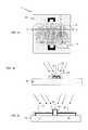
- FIG. 1 ashows a top view of a beginning structure in accordance with the invention
- FIG. 1 bshows a cross sectional view of the structure of FIG. 1 a;
- FIG. 2 ashows a top view of an intermediate structure in accordance with the invention
- FIG. 2 bshows a cross sectional view of the structure of FIG. 2 b
- FIG. 3 ashows a top view of a final structure in accordance with the invention
- FIGS. 3 b and 3 cshow cross sectional views of the structure of FIG. 3 a ;
- FIG. 4is a flow diagram of a design process used in semiconductor design, manufacture, and/or test.
- the inventionrelates to FinFETs and a method manufacture, and more particularly, to FinFETs merged with a metal and a method of manufacturing the same. More specifically, the present invention is directed to FinFET structures, which have reduced contact resistance compared to FinFETs formed using conventional epi FinFET source/drain processes.
- the present inventioneliminates unstable epitaxial growth of Si on the fin body which leads to high resistance and degradation in device performance. Instead, the present invention merges the fin bodies through chemical vapor deposition (CVD) of metal directly on the FinFETs.
- the metalhas a conductivity that is not dependent on thickness, which ensures more stable processes, eliminates high resistance of epi and, hence, does not lead to degradation of device performance.
- FIG. 1 ashows a top view of a beginning structure
- FIG. 1 bshows a cross sectional view of the structure of FIG. 1 a
- the structure 5includes a substrate 10 such as, for example, BOX, SOI, AlO 2 or any other suitable substrate.
- the substrate 10can be bulk silicon substrate or, more commonly, a silicon-on-insulator (SOI) wafer that includes an active SOI layer of a single crystal semiconductor, such as silicon, a semiconductor substrate, and a buried insulator layer, e.g., a buried oxide layer that separates and electrically isolates the semiconductor substrate from the SOI layer.
- SOIsilicon-on-insulator
- a plurality of FinFETs (fin bodies) 12is formed on the substrate 10 using conventional processes.
- the fin bodies 12are narrow vertical fin bodies of single crystal semiconductor material with vertically-projecting sidewalls.
- the fin bodies 12may be processed either by optical or e-beam lithographic processes in combination with trimming processes such as, for example, resist trimming, hard mask trimming or oxidation trimming.
- Another method of trimming utilized by the present inventionis sidewall image transfer (SIT) process, which provides very high-density structures that are independent of lithographic resolution and pitch.
- the SIT processis based upon a spacer that is formed on the sidewall of an optical defined structure, where the spacer is used as a mask to define the structure of the underlying layer or layers.
- Other methods of forming the finare also contemplated by the present invention such as, for example, as disclosed in U.S. Pat. No. 7,470,570 which is assigned to International Business Machines, Corp. U.S. Pat. No. 7,470,570 is incorporated by reference herein in its entirety.
- a gate 14is formed over the fin bodies 12 using conventional deposition, lithographic and etching processes.
- the gate 14is a poly or metal gate that intersects a channel region of the fin bodies and is isolated electrically from the fin bodies by a thin gate dielectric layer, e.g., spacer 16 .
- the spacer 16must be resistant to HF etching, is deposited on the sidewalls of the gate 14 using conventional deposition processes.
- the spacer 16is oxide, but can also be nitride or other dielectric materials. At opposite ends of the fin bodies are heavily-doped source/drain regions.
- the fin bodies 12undergo an implantation processes as represented by the arrows in FIG. 2 b .
- the implantation processincludes implanting a dopant such as, nFET and pFET extension, as well as NFET and pFET halos.
- the nFET extensioncan be, for example, As (1 keV to 6 keV) or P (0.5 keV to 3 keV), at a dosage of about 2e15+/ ⁇ 2e15 and tilt angle of about 0-20 degrees.
- the pFET extensioncan be, for example, B (0.5 keV to 2 keV) or BF 2 (2 keV to 6 keV), at a dosage of 2e15+/ ⁇ 2e15 and tilt angle of about 0-20 degrees.
- the nFET halocan be B (5 keV to 10 keV) or BF 2 (30 keV to 50 keV), at a dosage of about 4e13+/ ⁇ 2e13 and a tilt angle of about 10 to 30 degrees.
- the pFET halocan be, for example, As (30 keV to 50 keV) at a dosage of about 3e13+/ ⁇ 1e13 and a tilt angle of about 10 to 30 degrees.
- the structurethen undergoes an activation annealing process. After the annealing process, the fin bodies 12 undergo an optional pre-silicide clean process using, for example, dilute HF.
- a metal deposition processis performed on the fin bodies 12 .
- a CVD metal deposition processis performed to form a silicide 18 directly on the fin bodies 12 .
- the metalmay be tungsten or cobalt; although other metals are also contemplated by the present invention such as, for example, nickel.
- the metal 18may be deposited to a depth of about 10 nm to about 20 nm; although other dimensions are also contemplated by the invention.
- a silicidation anneal(e.g., rapid thermal anneal (RTA)) is performed at a temperature of about 300° C. to about 500° C.
- RTArapid thermal anneal
- the spacing between the fin bodies 12is about 30 nm to about 60 nm; although other dimensions are also contemplated by the present invention.
- the silicidewill provide a transition (superior contact area) between the fin bodies 12 and a subsequently deposited metal.
- FIG. 3 ashows a top view of a final structure in accordance with the invention
- FIGS. 3 b and 3 cshow cross sectional views of the structure of FIG. 3 a
- FIG. 3 bis a cross sectional view along line C-C of FIG. 3 a
- FIG. 3 cis a cross sectional view along line C′-C′ of FIG. 3 a
- the fin bodies 12may undergo an optional pre-metal clean using, for example, a dilute HF.
- a metal deposition processis performed to merge the fin bodies 12 .
- metal 20is deposited on the fin bodies 12 and gate structure 14 .
- the CVDis selective to the silicided fin bodies 12 .
- the metal 20may be, for example, tungsten or aluminum; although other metals such as, for example, nickel, are also contemplated by the present invention.
- Metals such as, for example, aluminumhave a very low sheet resistance, which improves overall device performance.
- the structurethen undergoes an optional annealing process to reflow the metal.
- the metal 20is deposited to such a thickness that the fin bodies 12 become merged.
- the thickness of the deposited metalcan be, for example, about 30 nm to 60 nm; although other dimensions are contemplated by the present invention depending on the spacing between the fin bodies 12 .
- any thickness that merges the fins 12 togethercan be used with the present invention.
- conductivity of the metalis not dependent on the thickness and, as such, the deposition of metal on the structure will not degrade device performance.
- the fin bodies 12undergo a source drain (S/D) implantation.
- the S/D implantmay be, for an nFET SD, As (10 keV to 30 keV) or P (5 keV to 15 keV) at a dosage of about 3e15+/ ⁇ 1e15 and a tilt angle of about 0-10 degrees.
- the S/D implant for a pFETmay be, for example, B (1 keV to 3 keV) or BF 2 (10 keV to 50 keV), at a dosage of about 3e15+/ ⁇ 1e15 and a tilt angle of about 0-10 degrees.
- the metalhas a conductivity that is not dependent on thickness, which ensures more stable processes, eliminates high resistance of epi and, hence, does not lead to degradation of device performance.
- FIG. 4shows a block diagram of an exemplary design flow 900 used for example, in semiconductor design, manufacturing, and/or test.
- Design flow 900may vary depending on the type of IC being designed.
- a design flow 900 for building an application specific IC (ASIC)may differ from a design flow 900 for designing a standard component or from a design flow 900 for instantiating the design into a programmable array, for example a programmable gate array (PGA) or a field programmable gate array (FPGA) offered by Alter® Inc. or Xilinx® Inc.
- PGAprogrammable gate array
- FPGAfield programmable gate array
- Design structure 920is preferably an input to a design process 910 and may come from an IP provider, a core developer, or other design company or may be generated by the operator of the design flow, or from other sources.
- Design structure 920comprises an embodiment of the invention as shown in FIGS. 1 a - 3 c in the form of schematics or HDL, a hardware-description language (e.g., Virology, VHDL, C, etc.).
- Design structure 920may be contained on one or more machine-readable media.
- design structure 920may be a text file or a graphical representation of an embodiment of the invention as shown in FIGS. 1 a - 3 c .
- Design process 910preferably synthesizes (or translates) embodiments of the invention as shown in FIGS. 1 a - 3 c into a net list 980 , where net list 980 is, for example, a list of wires, transistors, logic gates, control circuits, I/O, models, etc. that describes the connections to other elements and circuits in an integrated circuit design and recorded on at least one of machine readable media.
- the mediummay be a CD, a compact flash, other flash memory, a packet of data to be sent via the Internet, or other networking suitable means.
- the synthesismay be an iterative process in which net list 980 is resynthesized one or more times depending on design specifications and parameters for the circuit.
- Design process 910may include using a variety of inputs; for example, inputs from library elements 930 which may house a set of commonly used elements, circuits, and devices, including models, layouts, and symbolic representations, for a given manufacturing technology (e.g., different technology nodes, 32 nm, 45 nm, 90 nm, etc.), design specifications 940 , characterization data 950 , verification data 960 , design rules 970 , and test data files 985 (which may include test patterns and other testing information). Design process 910 may further include, for example, standard circuit design processes such as timing analysis, verification, design rule checking, place and route operations, etc.
- standard circuit design processessuch as timing analysis, verification, design rule checking, place and route operations, etc.
- Design process 910preferably translates an embodiment of the invention as shown in FIGS. 1 a - 3 c , along with any additional integrated circuit design or data (if applicable), into a second design structure 990 .
- Design structure 990resides on a storage medium in a data format used for the exchange of layout data of integrated circuits and/or symbolic data format (e.g. information stored in a GDSII (GDS2), GL1, OASIS, map files, or any other suitable format for storing such design structures).
- GDSIIGDS2
- GL1GL1, OASIS, map files, or any other suitable format for storing such design structures.
- Design structure 990may comprise information such as, for example, symbolic data, map files, test data files, design content files, manufacturing data, layout parameters, wires, levels of metal, vias, shapes, data for routing through the manufacturing line, and any other data required by a semiconductor manufacturer to produce embodiments of the invention as shown in FIGS. 1 a - 3 c .
- Design structure 990may then proceed to a stage 995 where, for example, design structure 990 : proceeds to tape-out, is released to manufacturing, is released to a mask house, is sent to another design house, is sent back to the customer, etc.
- the methods as described aboveis used in the fabrication of integrated circuit chips.
- the resulting integrated circuit chipscan be distributed by the fabricator in raw wafer form (that is, as a single wafer that has multiple unpackaged chips), as a bare die, or in a packaged form.
- the chipis mounted in a single chip package (such as a plastic carrier, with leads that are affixed to a motherboard or other higher level carrier) or in a multichip package (such as a ceramic carrier that has either or both surface interconnections or buried interconnections).
- the chipis then integrated with other chips, discrete circuit elements, and/or other signal processing devices as part of either (a) an intermediate product, such as a motherboard, or (b) an end product.
- the end productcan be any product that includes integrated circuit chips.
Landscapes
- Thin Film Transistor (AREA)
Abstract
Description
Claims (18)
Priority Applications (1)
| Application Number | Priority Date | Filing Date | Title |
|---|---|---|---|
| US12/574,296US8946028B2 (en) | 2009-10-06 | 2009-10-06 | Merged FinFETs and method of manufacturing the same |
Applications Claiming Priority (1)
| Application Number | Priority Date | Filing Date | Title |
|---|---|---|---|
| US12/574,296US8946028B2 (en) | 2009-10-06 | 2009-10-06 | Merged FinFETs and method of manufacturing the same |
Publications (2)
| Publication Number | Publication Date |
|---|---|
| US20110079855A1 US20110079855A1 (en) | 2011-04-07 |
| US8946028B2true US8946028B2 (en) | 2015-02-03 |
Family
ID=43822543
Family Applications (1)
| Application Number | Title | Priority Date | Filing Date |
|---|---|---|---|
| US12/574,296Expired - Fee RelatedUS8946028B2 (en) | 2009-10-06 | 2009-10-06 | Merged FinFETs and method of manufacturing the same |
Country Status (1)
| Country | Link |
|---|---|
| US (1) | US8946028B2 (en) |
Cited By (3)
| Publication number | Priority date | Publication date | Assignee | Title |
|---|---|---|---|---|
| US9564369B1 (en) | 2015-10-21 | 2017-02-07 | Samsung Electronics Co., Ltd. | Methods of manufacturing semiconductor devices including device isolation processes |
| US20180122646A1 (en)* | 2016-09-08 | 2018-05-03 | International Business Machines Corporation | Low resistance source-drain contacts using high temperature silicides |
| US20210018544A1 (en)* | 2017-08-22 | 2021-01-21 | Taiwan Semiconductor Manufacturing Co., Ltd. | Semiconductor test device and manufacturing method thereof |
Families Citing this family (17)
| Publication number | Priority date | Publication date | Assignee | Title |
|---|---|---|---|---|
| US8753964B2 (en)* | 2011-01-27 | 2014-06-17 | International Business Machines Corporation | FinFET structure having fully silicided fin |
| US8847293B2 (en)* | 2012-03-02 | 2014-09-30 | Taiwan Semiconductor Manufacturing Company, Ltd. | Gate structure for semiconductor device |
| US8946033B2 (en) | 2012-07-30 | 2015-02-03 | International Business Machines Corporation | Merged fin finFET with (100) sidewall surfaces and method of making same |
| US8946791B2 (en) | 2012-08-31 | 2015-02-03 | International Business Machines Corporation | Finfet with reduced parasitic capacitance |
| US8796085B2 (en) | 2012-10-12 | 2014-08-05 | Viktor Koldiaev | Vertical super-thin body semiconductor on dielectric wall devices and methods of their fabrication |
| US9117842B2 (en)* | 2013-03-13 | 2015-08-25 | Globalfoundries Inc. | Methods of forming contacts to source/drain regions of FinFET devices |
| US9082739B2 (en) | 2013-05-16 | 2015-07-14 | Samsung Electronics Co., Ltd. | Semiconductor device having test structure |
| KR102068980B1 (en) | 2013-08-01 | 2020-01-22 | 삼성전자 주식회사 | Semiconductor device and method for fabricating the same |
| US9023697B2 (en) | 2013-08-08 | 2015-05-05 | International Business Machines Corporation | 3D transistor channel mobility enhancement |
| US9196613B2 (en) | 2013-11-19 | 2015-11-24 | International Business Machines Corporation | Stress inducing contact metal in FinFET CMOS |
| KR102230198B1 (en) | 2014-09-23 | 2021-03-19 | 삼성전자주식회사 | Semiconductor device and method for manufacturing the same |
| KR102330757B1 (en) | 2015-03-30 | 2021-11-25 | 삼성전자주식회사 | Semiconductor devices and methods of manufacturing the same |
| KR102251060B1 (en) | 2015-04-06 | 2021-05-14 | 삼성전자주식회사 | Semiconductor devices and methods of manufacturing semiconductor devices |
| US9755073B1 (en)* | 2016-05-11 | 2017-09-05 | International Business Machines Corporation | Fabrication of vertical field effect transistor structure with strained channels |
| KR102365109B1 (en) | 2017-08-22 | 2022-02-18 | 삼성전자주식회사 | Integrated circuit devices |
| CN110164969A (en)* | 2018-02-13 | 2019-08-23 | 隽佾科技有限公司 | Wave field effect transistor structure |
| US20190267491A1 (en)* | 2018-02-27 | 2019-08-29 | Bruckewell Technology Corp., Ltd. | Wavy fet structure |
Citations (19)
| Publication number | Priority date | Publication date | Assignee | Title |
|---|---|---|---|---|
| US6096644A (en)* | 1998-09-08 | 2000-08-01 | Advanced Micro Devices, Inc. | Self-aligned contacts to source/drain silicon electrodes utilizing polysilicon and metal silicides |
| US6232224B1 (en)* | 1999-04-20 | 2001-05-15 | Nec Corporation | Method of manufacturing semiconductor device having reliable contact structure |
| US20020000621A1 (en)* | 1997-12-30 | 2002-01-03 | Robert H. Havemann | Enhancements to polysilicon gate |
| US6420784B2 (en)* | 1999-04-16 | 2002-07-16 | Micron Technology, Inc | Electrochemical cobalt silicide liner for metal contact fills and damascene processes |
| US6448167B1 (en)* | 2001-12-20 | 2002-09-10 | Taiwan Semiconductor Manufacturing Company | Process flow to reduce spacer undercut phenomena |
| US6867433B2 (en)* | 2003-04-30 | 2005-03-15 | Taiwan Semiconductor Manufacturing Company, Ltd. | Semiconductor-on-insulator chip incorporating strained-channel partially-depleted, fully-depleted, and multiple-gate transistors |
| US6960479B2 (en)* | 2001-07-20 | 2005-11-01 | Intel Corporation | Stacked ferroelectric memory device and method of making same |
| US7112495B2 (en) | 2003-08-15 | 2006-09-26 | Taiwan Semiconductor Manufacturing Company, Ltd. | Structure and method of a strained channel transistor and a second semiconductor component in an integrated circuit |
| US7180134B2 (en) | 2004-01-30 | 2007-02-20 | Taiwan Semiconductor Manufacturing Company, Ltd. | Methods and structures for planar and multiple-gate transistors formed on SOI |
| US7279375B2 (en)* | 2005-06-30 | 2007-10-09 | Intel Corporation | Block contact architectures for nanoscale channel transistors |
| US20080042219A1 (en)* | 2006-06-29 | 2008-02-21 | International Business Machines Corporation | finFET Device |
| US20080124868A1 (en) | 2005-08-03 | 2008-05-29 | International Business Machines Corporation | Fin-type field effect transistor |
| US7425740B2 (en) | 2005-10-07 | 2008-09-16 | Taiwan Semiconductor Manufacturing Company, Ltd. | Method and structure for a 1T-RAM bit cell and macro |
| US7456471B2 (en) | 2006-09-15 | 2008-11-25 | International Business Machines Corporation | Field effect transistor with raised source/drain fin straps |
| US20090001426A1 (en) | 2007-06-29 | 2009-01-01 | Kangguo Cheng | Integrated Fin-Local Interconnect Structure |
| US20090020819A1 (en) | 2007-07-16 | 2009-01-22 | Anderson Brent A | Fin-type field effect transistor structure with merged source/drain silicide and method of forming the structure |
| US20090101978A1 (en) | 2007-10-17 | 2009-04-23 | Anderson Brent A | Fin-type field effect transistor structure with merged source/drain silicide and method of forming the structure |
| US7608890B2 (en)* | 2005-06-14 | 2009-10-27 | Kabushiki Kaisha Toshiba | Semiconductor device and method of manufacturing semiconductor device |
| US7612416B2 (en)* | 2003-10-09 | 2009-11-03 | Nec Corporation | Semiconductor device having a conductive portion below an interlayer insulating film and method for producing the same |
- 2009
- 2009-10-06USUS12/574,296patent/US8946028B2/ennot_activeExpired - Fee Related
Patent Citations (19)
| Publication number | Priority date | Publication date | Assignee | Title |
|---|---|---|---|---|
| US20020000621A1 (en)* | 1997-12-30 | 2002-01-03 | Robert H. Havemann | Enhancements to polysilicon gate |
| US6096644A (en)* | 1998-09-08 | 2000-08-01 | Advanced Micro Devices, Inc. | Self-aligned contacts to source/drain silicon electrodes utilizing polysilicon and metal silicides |
| US6420784B2 (en)* | 1999-04-16 | 2002-07-16 | Micron Technology, Inc | Electrochemical cobalt silicide liner for metal contact fills and damascene processes |
| US6232224B1 (en)* | 1999-04-20 | 2001-05-15 | Nec Corporation | Method of manufacturing semiconductor device having reliable contact structure |
| US6960479B2 (en)* | 2001-07-20 | 2005-11-01 | Intel Corporation | Stacked ferroelectric memory device and method of making same |
| US6448167B1 (en)* | 2001-12-20 | 2002-09-10 | Taiwan Semiconductor Manufacturing Company | Process flow to reduce spacer undercut phenomena |
| US6867433B2 (en)* | 2003-04-30 | 2005-03-15 | Taiwan Semiconductor Manufacturing Company, Ltd. | Semiconductor-on-insulator chip incorporating strained-channel partially-depleted, fully-depleted, and multiple-gate transistors |
| US7112495B2 (en) | 2003-08-15 | 2006-09-26 | Taiwan Semiconductor Manufacturing Company, Ltd. | Structure and method of a strained channel transistor and a second semiconductor component in an integrated circuit |
| US7612416B2 (en)* | 2003-10-09 | 2009-11-03 | Nec Corporation | Semiconductor device having a conductive portion below an interlayer insulating film and method for producing the same |
| US7180134B2 (en) | 2004-01-30 | 2007-02-20 | Taiwan Semiconductor Manufacturing Company, Ltd. | Methods and structures for planar and multiple-gate transistors formed on SOI |
| US7608890B2 (en)* | 2005-06-14 | 2009-10-27 | Kabushiki Kaisha Toshiba | Semiconductor device and method of manufacturing semiconductor device |
| US7279375B2 (en)* | 2005-06-30 | 2007-10-09 | Intel Corporation | Block contact architectures for nanoscale channel transistors |
| US20080124868A1 (en) | 2005-08-03 | 2008-05-29 | International Business Machines Corporation | Fin-type field effect transistor |
| US7425740B2 (en) | 2005-10-07 | 2008-09-16 | Taiwan Semiconductor Manufacturing Company, Ltd. | Method and structure for a 1T-RAM bit cell and macro |
| US20080042219A1 (en)* | 2006-06-29 | 2008-02-21 | International Business Machines Corporation | finFET Device |
| US7456471B2 (en) | 2006-09-15 | 2008-11-25 | International Business Machines Corporation | Field effect transistor with raised source/drain fin straps |
| US20090001426A1 (en) | 2007-06-29 | 2009-01-01 | Kangguo Cheng | Integrated Fin-Local Interconnect Structure |
| US20090020819A1 (en) | 2007-07-16 | 2009-01-22 | Anderson Brent A | Fin-type field effect transistor structure with merged source/drain silicide and method of forming the structure |
| US20090101978A1 (en) | 2007-10-17 | 2009-04-23 | Anderson Brent A | Fin-type field effect transistor structure with merged source/drain silicide and method of forming the structure |
Non-Patent Citations (1)
| Title |
|---|
| Choi et al., "Large Scale Integration and Reliability Consideration of Triple Gate Transistors", IEDM, vol. 647, © 2004, pp. 27.6.1-27.6.4.* |
Cited By (8)
| Publication number | Priority date | Publication date | Assignee | Title |
|---|---|---|---|---|
| US9564369B1 (en) | 2015-10-21 | 2017-02-07 | Samsung Electronics Co., Ltd. | Methods of manufacturing semiconductor devices including device isolation processes |
| US20180122646A1 (en)* | 2016-09-08 | 2018-05-03 | International Business Machines Corporation | Low resistance source-drain contacts using high temperature silicides |
| US10685888B2 (en) | 2016-09-08 | 2020-06-16 | International Business Machines Corporation | Low resistance source-drain contacts using high temperature silicides |
| US10825740B2 (en)* | 2016-09-08 | 2020-11-03 | International Business Machines Corporation | Low resistance source-drain contacts using high temperature silicides |
| US11062956B2 (en) | 2016-09-08 | 2021-07-13 | International Business Machines Corporation | Low resistance source-drain contacts using high temperature silicides |
| US11088033B2 (en) | 2016-09-08 | 2021-08-10 | International Business Machines Corporation | Low resistance source-drain contacts using high temperature silicides |
| US20210018544A1 (en)* | 2017-08-22 | 2021-01-21 | Taiwan Semiconductor Manufacturing Co., Ltd. | Semiconductor test device and manufacturing method thereof |
| US11513145B2 (en)* | 2017-08-22 | 2022-11-29 | Taiwan Semiconductor Manufacturing Co., Ltd. | Semiconductor test device and manufacturing method thereof |
Also Published As
| Publication number | Publication date |
|---|---|
| US20110079855A1 (en) | 2011-04-07 |
Similar Documents
| Publication | Publication Date | Title |
|---|---|---|
| US8946028B2 (en) | Merged FinFETs and method of manufacturing the same | |
| US10566454B2 (en) | Self-aligned contact process enabled by low temperature | |
| US8461625B2 (en) | Carrier mobility enhanced channel devices and method of manufacture | |
| US8536705B2 (en) | Integrated circuit system with through silicon via and method of manufacture thereof | |
| CN103283016B (en) | Structure and method of manufacturing resistors according to FinFET process | |
| US8932949B2 (en) | FinFET structure and method to adjust threshold voltage in a FinFET structure | |
| US9231085B2 (en) | Semiconductor structure and methods of manufacture | |
| US10998270B2 (en) | Local interconnect for group IV source/drain regions | |
| US20210408283A1 (en) | Gate-all-around integrated circuit structures having strained source or drain structures on insulator | |
| US11888048B2 (en) | Gate oxide for nanosheet transistor devices | |
| CN111129019A (en) | Semiconductor device with a plurality of semiconductor chips | |
| US20230352590A1 (en) | Finfet device with partial interface dipole formation for reduction of gate induced drain leakage | |
| US20100019358A1 (en) | Semiconductor device and method of manufacturing | |
| US8941190B2 (en) | Semiconductor structures and methods of manufacture | |
| WO2019066879A1 (en) | Group iii-v semiconductor fuses and their methods of fabrication | |
| US7993989B2 (en) | Vertical spacer forming and related transistor | |
| US8552532B2 (en) | Self aligned structures and design structure thereof | |
| US20250113595A1 (en) | Multiple voltage threshold integrated circuit structure with local layout effect tuning | |
| WO2024037873A1 (en) | Backside contact for semiconductor device | |
| EP4505513A1 (en) | Nanosheet pull-up transistor in sram | |
| CN116153931A (en) | Semiconductor structure and manufacturing process thereof | |
| US12310061B2 (en) | Nanosheet transistor devices with different active channel widths | |
| US9093421B2 (en) | Implementing gate within a gate utilizing replacement metal gate process |
Legal Events
| Date | Code | Title | Description |
|---|---|---|---|
| AS | Assignment | Owner name:INTERNATIONAL BUSINESS MACHINES CORPORATION, NEW Y Free format text:ASSIGNMENT OF ASSIGNORS INTEREST;ASSIGNORS:CHAN, KEVIN K.;REN, ZHIBIN;WANG, XINHUI;AND OTHERS;SIGNING DATES FROM 20090923 TO 20091002;REEL/FRAME:023490/0247 | |
| STCF | Information on status: patent grant | Free format text:PATENTED CASE | |
| AS | Assignment | Owner name:GLOBALFOUNDRIES U.S. 2 LLC, NEW YORK Free format text:ASSIGNMENT OF ASSIGNORS INTEREST;ASSIGNOR:INTERNATIONAL BUSINESS MACHINES CORPORATION;REEL/FRAME:036550/0001 Effective date:20150629 | |
| AS | Assignment | Owner name:GLOBALFOUNDRIES INC., CAYMAN ISLANDS Free format text:ASSIGNMENT OF ASSIGNORS INTEREST;ASSIGNORS:GLOBALFOUNDRIES U.S. 2 LLC;GLOBALFOUNDRIES U.S. INC.;REEL/FRAME:036779/0001 Effective date:20150910 | |
| MAFP | Maintenance fee payment | Free format text:PAYMENT OF MAINTENANCE FEE, 4TH YEAR, LARGE ENTITY (ORIGINAL EVENT CODE: M1551) Year of fee payment:4 | |
| AS | Assignment | Owner name:WILMINGTON TRUST, NATIONAL ASSOCIATION, DELAWARE Free format text:SECURITY AGREEMENT;ASSIGNOR:GLOBALFOUNDRIES INC.;REEL/FRAME:049490/0001 Effective date:20181127 | |
| AS | Assignment | Owner name:GLOBALFOUNDRIES U.S. INC., CALIFORNIA Free format text:ASSIGNMENT OF ASSIGNORS INTEREST;ASSIGNOR:GLOBALFOUNDRIES INC.;REEL/FRAME:054633/0001 Effective date:20201022 | |
| AS | Assignment | Owner name:GLOBALFOUNDRIES INC., CAYMAN ISLANDS Free format text:RELEASE BY SECURED PARTY;ASSIGNOR:WILMINGTON TRUST, NATIONAL ASSOCIATION;REEL/FRAME:054636/0001 Effective date:20201117 | |
| AS | Assignment | Owner name:GLOBALFOUNDRIES U.S. INC., NEW YORK Free format text:RELEASE BY SECURED PARTY;ASSIGNOR:WILMINGTON TRUST, NATIONAL ASSOCIATION;REEL/FRAME:056987/0001 Effective date:20201117 | |
| FEPP | Fee payment procedure | Free format text:MAINTENANCE FEE REMINDER MAILED (ORIGINAL EVENT CODE: REM.); ENTITY STATUS OF PATENT OWNER: LARGE ENTITY | |
| LAPS | Lapse for failure to pay maintenance fees | Free format text:PATENT EXPIRED FOR FAILURE TO PAY MAINTENANCE FEES (ORIGINAL EVENT CODE: EXP.); ENTITY STATUS OF PATENT OWNER: LARGE ENTITY | |
| STCH | Information on status: patent discontinuation | Free format text:PATENT EXPIRED DUE TO NONPAYMENT OF MAINTENANCE FEES UNDER 37 CFR 1.362 | |
| FP | Lapsed due to failure to pay maintenance fee | Effective date:20230203 |