US8946020B2 - Method of forming controllably conductive oxide - Google Patents
Method of forming controllably conductive oxideDownload PDFInfo
- Publication number
- US8946020B2 US8946020B2US11/899,597US89959707AUS8946020B2US 8946020 B2US8946020 B2US 8946020B2US 89959707 AUS89959707 AUS 89959707AUS 8946020 B2US8946020 B2US 8946020B2
- Authority
- US
- United States
- Prior art keywords
- oxide
- electrode
- layer
- implanted
- conductivity
- Prior art date
- Legal status (The legal status is an assumption and is not a legal conclusion. Google has not performed a legal analysis and makes no representation as to the accuracy of the status listed.)
- Active, expires
Links
Images


Classifications
- H—ELECTRICITY
- H01—ELECTRIC ELEMENTS
- H01L—SEMICONDUCTOR DEVICES NOT COVERED BY CLASS H10
- H01L21/00—Processes or apparatus adapted for the manufacture or treatment of semiconductor or solid state devices or of parts thereof
- H01L21/02—Manufacture or treatment of semiconductor devices or of parts thereof
- H01L21/04—Manufacture or treatment of semiconductor devices or of parts thereof the devices having potential barriers, e.g. a PN junction, depletion layer or carrier concentration layer
- H01L21/18—Manufacture or treatment of semiconductor devices or of parts thereof the devices having potential barriers, e.g. a PN junction, depletion layer or carrier concentration layer the devices having semiconductor bodies comprising elements of Group IV of the Periodic Table or AIIIBV compounds with or without impurities, e.g. doping materials
- H01L21/30—Treatment of semiconductor bodies using processes or apparatus not provided for in groups H01L21/20 - H01L21/26
- H01L21/31—Treatment of semiconductor bodies using processes or apparatus not provided for in groups H01L21/20 - H01L21/26 to form insulating layers thereon, e.g. for masking or by using photolithographic techniques; After treatment of these layers; Selection of materials for these layers
- H01L21/314—Inorganic layers
- H01L21/316—Inorganic layers composed of oxides or glassy oxides or oxide based glass
- H01L21/3165—Inorganic layers composed of oxides or glassy oxides or oxide based glass formed by oxidation
- H01L21/31683—Inorganic layers composed of oxides or glassy oxides or oxide based glass formed by oxidation of metallic layers, e.g. Al deposited on the body, e.g. formation of multi-layer insulating structures
- H—ELECTRICITY
- H01—ELECTRIC ELEMENTS
- H01L—SEMICONDUCTOR DEVICES NOT COVERED BY CLASS H10
- H01L21/00—Processes or apparatus adapted for the manufacture or treatment of semiconductor or solid state devices or of parts thereof
- H01L21/02—Manufacture or treatment of semiconductor devices or of parts thereof
- H01L21/02104—Forming layers
- H01L21/02107—Forming insulating materials on a substrate
- H01L21/02225—Forming insulating materials on a substrate characterised by the process for the formation of the insulating layer
- H01L21/02227—Forming insulating materials on a substrate characterised by the process for the formation of the insulating layer formation by a process other than a deposition process
- H01L21/0223—Forming insulating materials on a substrate characterised by the process for the formation of the insulating layer formation by a process other than a deposition process formation by oxidation, e.g. oxidation of the substrate
- H01L21/02244—Forming insulating materials on a substrate characterised by the process for the formation of the insulating layer formation by a process other than a deposition process formation by oxidation, e.g. oxidation of the substrate of a metallic layer
- H01L45/04—
- H01L45/1233—
- H01L45/146—
- H01L45/1608—
- H01L45/165—
- H—ELECTRICITY
- H10—SEMICONDUCTOR DEVICES; ELECTRIC SOLID-STATE DEVICES NOT OTHERWISE PROVIDED FOR
- H10N—ELECTRIC SOLID-STATE DEVICES NOT OTHERWISE PROVIDED FOR
- H10N70/00—Solid-state devices having no potential barriers, and specially adapted for rectifying, amplifying, oscillating or switching
- H10N70/011—Manufacture or treatment of multistable switching devices
- H10N70/021—Formation of switching materials, e.g. deposition of layers
- H10N70/028—Formation of switching materials, e.g. deposition of layers by conversion of electrode material, e.g. oxidation
- H—ELECTRICITY
- H10—SEMICONDUCTOR DEVICES; ELECTRIC SOLID-STATE DEVICES NOT OTHERWISE PROVIDED FOR
- H10N—ELECTRIC SOLID-STATE DEVICES NOT OTHERWISE PROVIDED FOR
- H10N70/00—Solid-state devices having no potential barriers, and specially adapted for rectifying, amplifying, oscillating or switching
- H10N70/011—Manufacture or treatment of multistable switching devices
- H10N70/041—Modification of switching materials after formation, e.g. doping
- H10N70/043—Modification of switching materials after formation, e.g. doping by implantation
- H—ELECTRICITY
- H10—SEMICONDUCTOR DEVICES; ELECTRIC SOLID-STATE DEVICES NOT OTHERWISE PROVIDED FOR
- H10N—ELECTRIC SOLID-STATE DEVICES NOT OTHERWISE PROVIDED FOR
- H10N70/00—Solid-state devices having no potential barriers, and specially adapted for rectifying, amplifying, oscillating or switching
- H10N70/20—Multistable switching devices, e.g. memristors
- H10N70/25—Multistable switching devices, e.g. memristors based on bulk electronic defects, e.g. trapping of electrons
- H—ELECTRICITY
- H10—SEMICONDUCTOR DEVICES; ELECTRIC SOLID-STATE DEVICES NOT OTHERWISE PROVIDED FOR
- H10N—ELECTRIC SOLID-STATE DEVICES NOT OTHERWISE PROVIDED FOR
- H10N70/00—Solid-state devices having no potential barriers, and specially adapted for rectifying, amplifying, oscillating or switching
- H10N70/801—Constructional details of multistable switching devices
- H10N70/821—Device geometry
- H10N70/826—Device geometry adapted for essentially vertical current flow, e.g. sandwich or pillar type devices
- H—ELECTRICITY
- H10—SEMICONDUCTOR DEVICES; ELECTRIC SOLID-STATE DEVICES NOT OTHERWISE PROVIDED FOR
- H10N—ELECTRIC SOLID-STATE DEVICES NOT OTHERWISE PROVIDED FOR
- H10N70/00—Solid-state devices having no potential barriers, and specially adapted for rectifying, amplifying, oscillating or switching
- H10N70/801—Constructional details of multistable switching devices
- H10N70/881—Switching materials
- H10N70/883—Oxides or nitrides
- H10N70/8833—Binary metal oxides, e.g. TaOx
- H—ELECTRICITY
- H10—SEMICONDUCTOR DEVICES; ELECTRIC SOLID-STATE DEVICES NOT OTHERWISE PROVIDED FOR
- H10N—ELECTRIC SOLID-STATE DEVICES NOT OTHERWISE PROVIDED FOR
- H10N70/00—Solid-state devices having no potential barriers, and specially adapted for rectifying, amplifying, oscillating or switching
- H10N70/801—Constructional details of multistable switching devices
- H10N70/881—Switching materials
- H10N70/883—Oxides or nitrides
- H10N70/8836—Complex metal oxides, e.g. perovskites, spinels
- H—ELECTRICITY
- H10—SEMICONDUCTOR DEVICES; ELECTRIC SOLID-STATE DEVICES NOT OTHERWISE PROVIDED FOR
- H10N—ELECTRIC SOLID-STATE DEVICES NOT OTHERWISE PROVIDED FOR
- H10N70/00—Solid-state devices having no potential barriers, and specially adapted for rectifying, amplifying, oscillating or switching
- H10N70/20—Multistable switching devices, e.g. memristors
- H10N70/24—Multistable switching devices, e.g. memristors based on migration or redistribution of ionic species, e.g. anions, vacancies
Definitions
- This inventionrelates generally to electronic devices, and more particularly, to resistive memory devices.
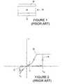
- FIG. 1illustrates a metal-insulator-metal (MIM) memory device 30 .
- the memory device 30includes an electrode 32 (for example copper), an insulating layer 34 (for example Ta 2 O 5 ) on the electrode 32 , and an electrode 36 (for example titanium) on the insulating layer 34 .
- an electrode 32for example copper
- an insulating layer 34for example Ta 2 O 5
- an electrode 36for example titanium
- an electrical potential V ris applied across the memory device 30 from a higher to a lower electrical potential in the direction from electrode 36 to electrode 32 .
- This electrical potentialis less than the electrical potential V pg applied across the memory device 30 for programming (see above). In this situation, the memory device 30 will readily conduct current, which indicates that the memory device 30 is in its programmed state.
- a positive voltageis applied to the electrode 32 , while the electrode 36 is held at ground, so that an electrical potential V er is applied across the memory device 30 from a higher to a lower electrical potential in the direction of from electrode 32 to electrode 36 .
- an electrical potential V eris applied across the memory device 30 from a higher to a lower electrical potential in the direction of from electrode 32 to electrode 36 .
- Application of this electrical potentialcauses the overall memory device 30 to adopt a high-resistance (erased) state illustrated at C.
- the electrical potential V ris again applied across the memory device 30 from a higher to a lower electrical potential in the direction from electrode 36 to electrode 32 as described above.
- the layer 34 (and memory device 30 ) in a high-resistance or substantially non-conductive statethe memory device 30 will not conduct significant current, which indicates that the memory device 30 is in its erased state.
- a memory device of this general typeshould be capable of use in a variety of conditions. For example, different device programming and erasing thresholds and on-resistance characteristics may be needed in different applications. Meanwhile, such a memory device should have rapid switching speed and show high stability in its programmed and erased states.
- a memory device of the general type described abovemay be readily configured so as to be usable in a variety of conditions, meanwhile exhibiting rapid switching speed and high data storage stability.
- the present method of fabricating a memory devicecomprises providing a first electrode, providing an alloy, oxidizing the alloy to provide an oxide layer, and providing a second electrode.
- the present method of fabricating a memory devicefurther comprises providing a first electrode, providing oxide, implanting material in the oxide to form a layer comprising oxide and implanted material having an oxygen deficiency and/or defects therein, and providing a second electrode.
- FIG. 1is a cross-sectional view of an above-described memory device
- FIG. 2is a plot of current vs. voltage illustrating operating characteristics of the memory device of FIG. 1 ;
- FIGS. 3-8illustrate various embodiments of the present invention.
- FIGS. 9-11are systems incorporating memory devices of the present type.
- FIGS. 3-5illustrate a first method for fabricating a metal-insulator-metal (MIM) resistive memory device of the type generally described above.
- an electrode 50for example copper
- an alloy 52 of selected metalsis deposited on the electrode 50 .
- the alloy 52includes tantalum and titanium in a mixture thereof.
- An oxidation step(for example thermal oxidation, plasma-assisted oxidation, or UV-light assisted oxidation) is undertaken to fully oxidize the alloy to form an oxide layer 54 (which is a mixture of titanium oxide and tantalum oxide, i.e., TiO 2 and Ta 2 O 5 ) on and in contact with the electrode 50 ( FIG. 4 ).
- a second electrode 56for example titanium is provided on and in contact with the oxide layer 54 to form the metal-insulator-metal (MIM) memory device 58 ( FIG. 5 ).
- the content of the oxide layerdepends 54 on the particular metals and proportions thereof making up the alloy 52 .
- the oxide layer 54 made up of the mixture of TiO 2 and Ta 2 O 5has operational characteristics which are different from that of the Ta 2 O 5 layer 34 of the previously described device.
- the operational characteristics of the overall memory device 58will depend on the particular metals and proportions thereof making up the alloy 54 .
- the operational characteristics of the fabricated memory device 58i.e., for example, program and erase voltages, on-resistance characteristics, and device stability may be based on the selected content of the alloy 54 as required.
- FIGS. 6-8illustrate various other embodiments of the invention.
- an electrode 60for example copper
- an oxide 62in this particular embodiment Ta 2 O 5
- a thin metal protective layer 64for example, aluminum, may then be deposited on and in contact with the oxide 62 .
- an implantation step for implanting material through the layer 64 and into the oxide 62is undertaken. This implantation step may take a number of forms.
- the implanted materialmay be titanium, nitrogen, or silicon.
- the implanted materialmay further for example be tantalum, which also will create a layer 66 comprising oxide and the implanted material having an overall oxygen deficiency by providing an excess of metal atoms for the oxygen present in the layer.
- the protective layer 64is included in order to seal out atmospheric oxygen in order to retain the oxygen-deficient state of the layer 66 .
- a second electrode 68(for example titanium) is provided on and in contact with the protective layer 64 to form the metal-insulator-metal (MIM) memory device 70 ( FIG. 8 ).
- the implantation stepalso causes damage to the oxide 62 , causing defects in the layer 66 comprising oxide and the implanted material so as to increase the conductivity thereof.
- materials for implantationmay be selected to cause damage to the oxide 62 without causing an oxygen deficiency therein (for example inert implant materials such as argon, krypton or xenon). Indeed, oxygen itself may be implanted for this purpose.
- the operational characteristics of the fabricated memory device 70i.e., for example, program and erase voltages, on-resistance characteristics, and device stability and may be based on the content of the implanted material as required.
- FIG. 9illustrates a system 200 utilizing memory devices as described above.
- the system 200includes hand-held devices 202 in the form of cell phones, which communicate through an intermediate apparatus such as a tower 204 (shown) and/or a satellite. Signals are provided from one cell phone to the other through the tower 204 .
- a cell phone with advantageuses memory devices of the type described above for data storage, for example names, telephone number and other data.
- memory devicesfor example names, telephone number and other data.
- One skilled in the artwill readily understand the advantage of using such memory devices in other hand-held devices 202 which utilize data storage, such as portable media players, personal digital assistants, digital cameras and the like.
- FIG. 10illustrates another system 300 utilizing memory devices as described above.
- the system 300includes a vehicle 302 having an engine 304 controlled by an electronic control unit 306 .
- the electronic control unit 306with advantage uses memory devices of the type described above for data storage, for example data relating to engine and vehicle operating conditions.
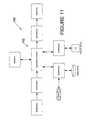
- FIG. 11illustrates yet another system 400 utilizing memory devices as described above.
- This system 400is a computer 402 which includes an input in the form of a keyboard, and a microprocessor for receiving signals from the keyboard through an interface.
- the microprocessoralso communicates with a CDROM drive, a hard drive, and a floppy drive through interfaces. Output from the microprocessor is provided to a monitor through an interface.
- memorywhich may take the form of ROM, RAM, flash and/or other forms of memory.
- the memory with advantageuses memory devices of the type described above for storage of any data which is of use.
Landscapes
- Engineering & Computer Science (AREA)
- Manufacturing & Machinery (AREA)
- Physics & Mathematics (AREA)
- Condensed Matter Physics & Semiconductors (AREA)
- General Physics & Mathematics (AREA)
- Computer Hardware Design (AREA)
- Microelectronics & Electronic Packaging (AREA)
- Power Engineering (AREA)
- Chemical & Material Sciences (AREA)
- Materials Engineering (AREA)
- Semiconductor Memories (AREA)
Abstract
Description
Claims (16)
Priority Applications (3)
| Application Number | Priority Date | Filing Date | Title |
|---|---|---|---|
| US11/899,597US8946020B2 (en) | 2007-09-06 | 2007-09-06 | Method of forming controllably conductive oxide |
| US14/612,083US9461247B2 (en) | 2007-09-06 | 2015-02-02 | Method of forming controllably conductive oxide |
| US15/258,234US10147877B2 (en) | 2007-09-06 | 2016-09-07 | Method of forming controllably conductive oxide |
Applications Claiming Priority (1)
| Application Number | Priority Date | Filing Date | Title |
|---|---|---|---|
| US11/899,597US8946020B2 (en) | 2007-09-06 | 2007-09-06 | Method of forming controllably conductive oxide |
Related Child Applications (1)
| Application Number | Title | Priority Date | Filing Date |
|---|---|---|---|
| US14/612,083DivisionUS9461247B2 (en) | 2007-09-06 | 2015-02-02 | Method of forming controllably conductive oxide |
Publications (2)
| Publication Number | Publication Date |
|---|---|
| US20090067213A1 US20090067213A1 (en) | 2009-03-12 |
| US8946020B2true US8946020B2 (en) | 2015-02-03 |
Family
ID=40431642
Family Applications (3)
| Application Number | Title | Priority Date | Filing Date |
|---|---|---|---|
| US11/899,597Active2028-01-13US8946020B2 (en) | 2007-09-06 | 2007-09-06 | Method of forming controllably conductive oxide |
| US14/612,083ActiveUS9461247B2 (en) | 2007-09-06 | 2015-02-02 | Method of forming controllably conductive oxide |
| US15/258,234ActiveUS10147877B2 (en) | 2007-09-06 | 2016-09-07 | Method of forming controllably conductive oxide |
Family Applications After (2)
| Application Number | Title | Priority Date | Filing Date |
|---|---|---|---|
| US14/612,083ActiveUS9461247B2 (en) | 2007-09-06 | 2015-02-02 | Method of forming controllably conductive oxide |
| US15/258,234ActiveUS10147877B2 (en) | 2007-09-06 | 2016-09-07 | Method of forming controllably conductive oxide |
Country Status (1)
| Country | Link |
|---|---|
| US (3) | US8946020B2 (en) |
Families Citing this family (5)
| Publication number | Priority date | Publication date | Assignee | Title |
|---|---|---|---|---|
| KR100847309B1 (en)* | 2007-02-27 | 2008-07-21 | 삼성전자주식회사 | Manufacturing method of nonvolatile memory device |
| US8062918B2 (en)* | 2008-05-01 | 2011-11-22 | Intermolecular, Inc. | Surface treatment to improve resistive-switching characteristics |
| US8313996B2 (en)* | 2010-09-22 | 2012-11-20 | Micron Technology, Inc. | Reactive metal implated oxide based memory |
| JP7382608B1 (en)* | 2022-05-31 | 2023-11-17 | 国立大学法人東京農工大学 | Fixed charge expression method, thin film transistor manufacturing method, and thin film transistor |
| JP7464863B2 (en)* | 2022-05-31 | 2024-04-10 | 日新電機株式会社 | Fixed charge control method, thin film transistor manufacturing method and thin film transistor |
Citations (7)
| Publication number | Priority date | Publication date | Assignee | Title |
|---|---|---|---|---|
| US4297782A (en)* | 1976-11-27 | 1981-11-03 | Fujitsu Limited | Method of manufacturing semiconductor devices |
| US20040161888A1 (en)* | 2002-08-02 | 2004-08-19 | Unity Semiconductor Corporation | Multi-resistive state material that uses dopants |
| US20040169255A1 (en)* | 2003-02-28 | 2004-09-02 | Masahiro Kiyotoshi | Semiconductor device and method of manufacturing same |
| US20070114508A1 (en)* | 2005-11-23 | 2007-05-24 | Matrix Semiconductor, Inc. | Reversible resistivity-switching metal oxide or nitride layer with added metal |
| US20070267675A1 (en)* | 2006-05-19 | 2007-11-22 | Samsung Electronics Co., Ltd. | Nonvolatile memory devices including oxygen-deficient metal oxide layers and methods of manufacturing the same |
| US7306988B1 (en)* | 2005-02-22 | 2007-12-11 | Advanced Micro Devices, Inc. | Memory cell and method of making the memory cell |
| US20080185567A1 (en)* | 2007-02-05 | 2008-08-07 | Nitin Kumar | Methods for forming resistive switching memory elements |
Family Cites Families (12)
| Publication number | Priority date | Publication date | Assignee | Title |
|---|---|---|---|---|
| US6366070B1 (en) | 2001-07-12 | 2002-04-02 | Analog Devices, Inc. | Switching voltage regulator with dual modulation control scheme |
| WO2003017282A1 (en)* | 2001-08-13 | 2003-02-27 | Advanced Micro Devices, Inc. | Memory cell |
| FR2835664B1 (en) | 2002-02-04 | 2004-04-16 | St Microelectronics Sa | METHOD OF GENERATING A VOLTAGE RAMP AT THE TERMINALS OF A CAPACITOR, AND CORRESPONDING ELECTRONIC DEVICE, IN PARTICULAR FOR A CUT-OFF POWER SUPPLY OF A CELLULAR MOBILE TELEPHONE |
| ITVA20020038A1 (en) | 2002-05-30 | 2003-12-01 | St Microelectronics Srl | VOLTAGE REGULATOR |
| JP3732173B2 (en) | 2002-11-18 | 2006-01-05 | ローム株式会社 | Power supply device and liquid crystal display device using the same |
| TW200608708A (en) | 2004-08-26 | 2006-03-01 | Richtek Techohnology Corp | Current-mode control converter with fixed frequency, and method thereof |
| TWI263874B (en) | 2004-09-09 | 2006-10-11 | Richtek Technology Corp | A voltage modulator of a low gain current model and the control method thereof |
| JP4311564B2 (en) | 2005-03-10 | 2009-08-12 | 富士通マイクロエレクトロニクス株式会社 | Control circuit and control method of current mode control type DC-DC converter |
| US7425819B2 (en) | 2005-06-16 | 2008-09-16 | Microsemi Corporation | Slope compensation circuit |
| GB2437556B (en) | 2006-04-26 | 2011-03-23 | Wolfson Microelectronics Plc | Improvements in switching regulator circuits |
| US7952337B2 (en) | 2006-12-18 | 2011-05-31 | Decicon, Inc. | Hybrid DC-DC switching regulator circuit |
| KR101357006B1 (en) | 2007-01-18 | 2014-01-29 | 페어차일드코리아반도체 주식회사 | Converter and the driving method thereof |
- 2007
- 2007-09-06USUS11/899,597patent/US8946020B2/enactiveActive
- 2015
- 2015-02-02USUS14/612,083patent/US9461247B2/enactiveActive
- 2016
- 2016-09-07USUS15/258,234patent/US10147877B2/enactiveActive
Patent Citations (7)
| Publication number | Priority date | Publication date | Assignee | Title |
|---|---|---|---|---|
| US4297782A (en)* | 1976-11-27 | 1981-11-03 | Fujitsu Limited | Method of manufacturing semiconductor devices |
| US20040161888A1 (en)* | 2002-08-02 | 2004-08-19 | Unity Semiconductor Corporation | Multi-resistive state material that uses dopants |
| US20040169255A1 (en)* | 2003-02-28 | 2004-09-02 | Masahiro Kiyotoshi | Semiconductor device and method of manufacturing same |
| US7306988B1 (en)* | 2005-02-22 | 2007-12-11 | Advanced Micro Devices, Inc. | Memory cell and method of making the memory cell |
| US20070114508A1 (en)* | 2005-11-23 | 2007-05-24 | Matrix Semiconductor, Inc. | Reversible resistivity-switching metal oxide or nitride layer with added metal |
| US20070267675A1 (en)* | 2006-05-19 | 2007-11-22 | Samsung Electronics Co., Ltd. | Nonvolatile memory devices including oxygen-deficient metal oxide layers and methods of manufacturing the same |
| US20080185567A1 (en)* | 2007-02-05 | 2008-08-07 | Nitin Kumar | Methods for forming resistive switching memory elements |
Also Published As
| Publication number | Publication date |
|---|---|
| US20160380195A1 (en) | 2016-12-29 |
| US10147877B2 (en) | 2018-12-04 |
| US20090067213A1 (en) | 2009-03-12 |
| US9461247B2 (en) | 2016-10-04 |
| US20150144857A1 (en) | 2015-05-28 |
Similar Documents
| Publication | Publication Date | Title |
|---|---|---|
| US10147877B2 (en) | Method of forming controllably conductive oxide | |
| US7521704B2 (en) | Memory device using multi-layer with a graded resistance change | |
| AU763809B2 (en) | Programmable microelectronic devices and methods of forming and programming same | |
| US7511294B2 (en) | Resistive memory element with shortened erase time | |
| US7423906B2 (en) | Integrated circuit having a memory cell | |
| US8279658B2 (en) | Method of programming variable resistance element and nonvolatile storage device | |
| US8675393B2 (en) | Method for driving non-volatile memory element, and non-volatile memory device | |
| KR20100089857A (en) | Memory cell | |
| JP5270044B2 (en) | Nonvolatile memory element manufacturing method and nonvolatile memory element | |
| JPWO2008081742A1 (en) | Resistance change element, resistance change memory device, and resistance change device | |
| CN1664957A (en) | storage device | |
| US7583525B2 (en) | Method of driving storage device | |
| US20110242874A1 (en) | Resistive memory and method for controlling operations of the same | |
| CN109791791B (en) | Nonvolatile memory device and driving method | |
| WO2002082452A2 (en) | Microelectronic device, structure, and system, including a memory structure having a variable programmable property and method of forming the same | |
| US8717803B2 (en) | Metal-insulator-metal-insulator-metal (MIMIM) memory device | |
| US7790497B2 (en) | Method to prevent alloy formation when forming layered metal oxides by metal oxidation | |
| JP2007311014A (en) | Memory element drive circuit | |
| US7706168B2 (en) | Erase, programming and leakage characteristics of a resistive memory device | |
| US8373148B2 (en) | Memory device with improved performance | |
| US20070210297A1 (en) | Electrical structure with a solid state electrolyte layer, memory with a memory cell and method for fabricating the electrical structure | |
| US8093698B2 (en) | Gettering/stop layer for prevention of reduction of insulating oxide in metal-insulator-metal device | |
| KR102226791B1 (en) | A resistive switching memory which eliminates erase operations | |
| US7935949B2 (en) | Switching device with solid electrolyte layer | |
| WO2008054572A1 (en) | Method of selecting operating characteristics of a resistive memory device |
Legal Events
| Date | Code | Title | Description |
|---|---|---|---|
| AS | Assignment | Owner name:SPANSION, CALIFORNIA Free format text:ASSIGNMENT OF ASSIGNORS INTEREST;ASSIGNORS:BUYNOSKI, MATTHEW;CHOI, SEUNGMOO;GOPALAN, CHAKRAVARTHY;AND OTHERS;REEL/FRAME:019833/0043;SIGNING DATES FROM 20070811 TO 20070824 Owner name:SPANSION, CALIFORNIA Free format text:ASSIGNMENT OF ASSIGNORS INTEREST;ASSIGNORS:BUYNOSKI, MATTHEW;CHOI, SEUNGMOO;GOPALAN, CHAKRAVARTHY;AND OTHERS;SIGNING DATES FROM 20070811 TO 20070824;REEL/FRAME:019833/0043 | |
| AS | Assignment | Owner name:BARCLAYS BANK PLC,NEW YORK Free format text:SECURITY AGREEMENT;ASSIGNORS:SPANSION LLC;SPANSION INC.;SPANSION TECHNOLOGY INC.;AND OTHERS;REEL/FRAME:024522/0338 Effective date:20100510 Owner name:BARCLAYS BANK PLC, NEW YORK Free format text:SECURITY AGREEMENT;ASSIGNORS:SPANSION LLC;SPANSION INC.;SPANSION TECHNOLOGY INC.;AND OTHERS;REEL/FRAME:024522/0338 Effective date:20100510 | |
| STCF | Information on status: patent grant | Free format text:PATENTED CASE | |
| AS | Assignment | Owner name:SPANSION LLC, CALIFORNIA Free format text:RELEASE BY SECURED PARTY;ASSIGNOR:BARCLAYS BANK PLC;REEL/FRAME:035201/0159 Effective date:20150312 Owner name:SPANSION INC., CALIFORNIA Free format text:RELEASE BY SECURED PARTY;ASSIGNOR:BARCLAYS BANK PLC;REEL/FRAME:035201/0159 Effective date:20150312 Owner name:SPANSION TECHNOLOGY LLC, CALIFORNIA Free format text:RELEASE BY SECURED PARTY;ASSIGNOR:BARCLAYS BANK PLC;REEL/FRAME:035201/0159 Effective date:20150312 | |
| AS | Assignment | Owner name:MORGAN STANLEY SENIOR FUNDING, INC., NEW YORK Free format text:SECURITY INTEREST;ASSIGNORS:CYPRESS SEMICONDUCTOR CORPORATION;SPANSION LLC;REEL/FRAME:035240/0429 Effective date:20150312 | |
| MAFP | Maintenance fee payment | Free format text:PAYMENT OF MAINTENANCE FEE, 4TH YEAR, LARGE ENTITY (ORIGINAL EVENT CODE: M1551) Year of fee payment:4 | |
| AS | Assignment | Owner name:MUFG UNION BANK, N.A., CALIFORNIA Free format text:ASSIGNMENT AND ASSUMPTION OF SECURITY INTEREST IN INTELLECTUAL PROPERTY;ASSIGNOR:MORGAN STANLEY SENIOR FUNDING, INC.;REEL/FRAME:050896/0366 Effective date:20190731 | |
| AS | Assignment | Owner name:MORGAN STANLEY SENIOR FUNDING, INC., NEW YORK Free format text:CORRECTIVE ASSIGNMENT TO CORRECT THE 8647899 PREVIOUSLY RECORDED ON REEL 035240 FRAME 0429. ASSIGNOR(S) HEREBY CONFIRMS THE SECURITY INTERST;ASSIGNORS:CYPRESS SEMICONDUCTOR CORPORATION;SPANSION LLC;REEL/FRAME:058002/0470 Effective date:20150312 | |
| AS | Assignment | Owner name:SPANSION LLC, CALIFORNIA Free format text:RELEASE BY SECURED PARTY;ASSIGNOR:MUFG UNION BANK, N.A.;REEL/FRAME:059410/0438 Effective date:20200416 Owner name:CYPRESS SEMICONDUCTOR CORPORATION, CALIFORNIA Free format text:RELEASE BY SECURED PARTY;ASSIGNOR:MUFG UNION BANK, N.A.;REEL/FRAME:059410/0438 Effective date:20200416 | |
| MAFP | Maintenance fee payment | Free format text:PAYMENT OF MAINTENANCE FEE, 8TH YEAR, LARGE ENTITY (ORIGINAL EVENT CODE: M1552); ENTITY STATUS OF PATENT OWNER: LARGE ENTITY Year of fee payment:8 |