US8945339B2 - Film formation apparatus - Google Patents
Film formation apparatusDownload PDFInfo
- Publication number
- US8945339B2 US8945339B2US13/283,869US201113283869AUS8945339B2US 8945339 B2US8945339 B2US 8945339B2US 201113283869 AUS201113283869 AUS 201113283869AUS 8945339 B2US8945339 B2US 8945339B2
- Authority
- US
- United States
- Prior art keywords
- gas
- process chamber
- film
- gas supply
- supplying
- Prior art date
- Legal status (The legal status is an assumption and is not a legal conclusion. Google has not performed a legal analysis and makes no representation as to the accuracy of the status listed.)
- Active, expires
Links
Images


Classifications
- H—ELECTRICITY
- H01—ELECTRIC ELEMENTS
- H01L—SEMICONDUCTOR DEVICES NOT COVERED BY CLASS H10
- H01L21/00—Processes or apparatus adapted for the manufacture or treatment of semiconductor or solid state devices or of parts thereof
- H01L21/02—Manufacture or treatment of semiconductor devices or of parts thereof
- H01L21/02041—Cleaning
- H01L21/02057—Cleaning during device manufacture
- C—CHEMISTRY; METALLURGY
- C23—COATING METALLIC MATERIAL; COATING MATERIAL WITH METALLIC MATERIAL; CHEMICAL SURFACE TREATMENT; DIFFUSION TREATMENT OF METALLIC MATERIAL; COATING BY VACUUM EVAPORATION, BY SPUTTERING, BY ION IMPLANTATION OR BY CHEMICAL VAPOUR DEPOSITION, IN GENERAL; INHIBITING CORROSION OF METALLIC MATERIAL OR INCRUSTATION IN GENERAL
- C23C—COATING METALLIC MATERIAL; COATING MATERIAL WITH METALLIC MATERIAL; SURFACE TREATMENT OF METALLIC MATERIAL BY DIFFUSION INTO THE SURFACE, BY CHEMICAL CONVERSION OR SUBSTITUTION; COATING BY VACUUM EVAPORATION, BY SPUTTERING, BY ION IMPLANTATION OR BY CHEMICAL VAPOUR DEPOSITION, IN GENERAL
- C23C16/00—Chemical coating by decomposition of gaseous compounds, without leaving reaction products of surface material in the coating, i.e. chemical vapour deposition [CVD] processes
- C23C16/02—Pretreatment of the material to be coated
- C23C16/0272—Deposition of sub-layers, e.g. to promote the adhesion of the main coating
- C—CHEMISTRY; METALLURGY
- C23—COATING METALLIC MATERIAL; COATING MATERIAL WITH METALLIC MATERIAL; CHEMICAL SURFACE TREATMENT; DIFFUSION TREATMENT OF METALLIC MATERIAL; COATING BY VACUUM EVAPORATION, BY SPUTTERING, BY ION IMPLANTATION OR BY CHEMICAL VAPOUR DEPOSITION, IN GENERAL; INHIBITING CORROSION OF METALLIC MATERIAL OR INCRUSTATION IN GENERAL
- C23C—COATING METALLIC MATERIAL; COATING MATERIAL WITH METALLIC MATERIAL; SURFACE TREATMENT OF METALLIC MATERIAL BY DIFFUSION INTO THE SURFACE, BY CHEMICAL CONVERSION OR SUBSTITUTION; COATING BY VACUUM EVAPORATION, BY SPUTTERING, BY ION IMPLANTATION OR BY CHEMICAL VAPOUR DEPOSITION, IN GENERAL
- C23C16/00—Chemical coating by decomposition of gaseous compounds, without leaving reaction products of surface material in the coating, i.e. chemical vapour deposition [CVD] processes
- C23C16/04—Coating on selected surface areas, e.g. using masks
- C23C16/045—Coating cavities or hollow spaces, e.g. interior of tubes; Infiltration of porous substrates
- C—CHEMISTRY; METALLURGY
- C23—COATING METALLIC MATERIAL; COATING MATERIAL WITH METALLIC MATERIAL; CHEMICAL SURFACE TREATMENT; DIFFUSION TREATMENT OF METALLIC MATERIAL; COATING BY VACUUM EVAPORATION, BY SPUTTERING, BY ION IMPLANTATION OR BY CHEMICAL VAPOUR DEPOSITION, IN GENERAL; INHIBITING CORROSION OF METALLIC MATERIAL OR INCRUSTATION IN GENERAL
- C23C—COATING METALLIC MATERIAL; COATING MATERIAL WITH METALLIC MATERIAL; SURFACE TREATMENT OF METALLIC MATERIAL BY DIFFUSION INTO THE SURFACE, BY CHEMICAL CONVERSION OR SUBSTITUTION; COATING BY VACUUM EVAPORATION, BY SPUTTERING, BY ION IMPLANTATION OR BY CHEMICAL VAPOUR DEPOSITION, IN GENERAL
- C23C16/00—Chemical coating by decomposition of gaseous compounds, without leaving reaction products of surface material in the coating, i.e. chemical vapour deposition [CVD] processes
- C23C16/22—Chemical coating by decomposition of gaseous compounds, without leaving reaction products of surface material in the coating, i.e. chemical vapour deposition [CVD] processes characterised by the deposition of inorganic material, other than metallic material
- C23C16/24—Deposition of silicon only
- H—ELECTRICITY
- H01—ELECTRIC ELEMENTS
- H01L—SEMICONDUCTOR DEVICES NOT COVERED BY CLASS H10
- H01L21/00—Processes or apparatus adapted for the manufacture or treatment of semiconductor or solid state devices or of parts thereof
- H01L21/02—Manufacture or treatment of semiconductor devices or of parts thereof
- H01L21/02104—Forming layers
- H01L21/02365—Forming inorganic semiconducting materials on a substrate
- H01L21/02367—Substrates
- H01L21/0237—Materials
- H01L21/02425—Conductive materials, e.g. metallic silicides
- H—ELECTRICITY
- H01—ELECTRIC ELEMENTS
- H01L—SEMICONDUCTOR DEVICES NOT COVERED BY CLASS H10
- H01L21/00—Processes or apparatus adapted for the manufacture or treatment of semiconductor or solid state devices or of parts thereof
- H01L21/02—Manufacture or treatment of semiconductor devices or of parts thereof
- H01L21/02104—Forming layers
- H01L21/02365—Forming inorganic semiconducting materials on a substrate
- H01L21/02436—Intermediate layers between substrates and deposited layers
- H01L21/02439—Materials
- H01L21/02441—Group 14 semiconducting materials
- H01L21/0245—Silicon, silicon germanium, germanium
- H—ELECTRICITY
- H01—ELECTRIC ELEMENTS
- H01L—SEMICONDUCTOR DEVICES NOT COVERED BY CLASS H10
- H01L21/00—Processes or apparatus adapted for the manufacture or treatment of semiconductor or solid state devices or of parts thereof
- H01L21/02—Manufacture or treatment of semiconductor devices or of parts thereof
- H01L21/02104—Forming layers
- H01L21/02365—Forming inorganic semiconducting materials on a substrate
- H01L21/02518—Deposited layers
- H01L21/02521—Materials
- H01L21/02524—Group 14 semiconducting materials
- H01L21/02532—Silicon, silicon germanium, germanium
- H—ELECTRICITY
- H01—ELECTRIC ELEMENTS
- H01L—SEMICONDUCTOR DEVICES NOT COVERED BY CLASS H10
- H01L21/00—Processes or apparatus adapted for the manufacture or treatment of semiconductor or solid state devices or of parts thereof
- H01L21/02—Manufacture or treatment of semiconductor devices or of parts thereof
- H01L21/02104—Forming layers
- H01L21/02365—Forming inorganic semiconducting materials on a substrate
- H01L21/02518—Deposited layers
- H01L21/0257—Doping during depositing
- H01L21/02573—Conductivity type
- H01L21/02576—N-type
- H—ELECTRICITY
- H01—ELECTRIC ELEMENTS
- H01L—SEMICONDUCTOR DEVICES NOT COVERED BY CLASS H10
- H01L21/00—Processes or apparatus adapted for the manufacture or treatment of semiconductor or solid state devices or of parts thereof
- H01L21/02—Manufacture or treatment of semiconductor devices or of parts thereof
- H01L21/02104—Forming layers
- H01L21/02365—Forming inorganic semiconducting materials on a substrate
- H01L21/02612—Formation types
- H01L21/02617—Deposition types
- H01L21/0262—Reduction or decomposition of gaseous compounds, e.g. CVD
- H—ELECTRICITY
- H01—ELECTRIC ELEMENTS
- H01L—SEMICONDUCTOR DEVICES NOT COVERED BY CLASS H10
- H01L21/00—Processes or apparatus adapted for the manufacture or treatment of semiconductor or solid state devices or of parts thereof
- H01L21/02—Manufacture or treatment of semiconductor devices or of parts thereof
- H01L21/02104—Forming layers
- H01L21/02365—Forming inorganic semiconducting materials on a substrate
- H01L21/02612—Formation types
- H01L21/02617—Deposition types
- H01L21/02636—Selective deposition, e.g. simultaneous growth of mono- and non-monocrystalline semiconductor materials
- H01L21/02639—Preparation of substrate for selective deposition
- H—ELECTRICITY
- H01—ELECTRIC ELEMENTS
- H01L—SEMICONDUCTOR DEVICES NOT COVERED BY CLASS H10
- H01L21/00—Processes or apparatus adapted for the manufacture or treatment of semiconductor or solid state devices or of parts thereof
- H01L21/02—Manufacture or treatment of semiconductor devices or of parts thereof
- H01L21/04—Manufacture or treatment of semiconductor devices or of parts thereof the devices having potential barriers, e.g. a PN junction, depletion layer or carrier concentration layer
- H01L21/18—Manufacture or treatment of semiconductor devices or of parts thereof the devices having potential barriers, e.g. a PN junction, depletion layer or carrier concentration layer the devices having semiconductor bodies comprising elements of Group IV of the Periodic Table or AIIIBV compounds with or without impurities, e.g. doping materials
- H01L21/28—Manufacture of electrodes on semiconductor bodies using processes or apparatus not provided for in groups H01L21/20 - H01L21/268
- H01L21/283—Deposition of conductive or insulating materials for electrodes conducting electric current
- H01L21/285—Deposition of conductive or insulating materials for electrodes conducting electric current from a gas or vapour, e.g. condensation
- H01L21/28506—Deposition of conductive or insulating materials for electrodes conducting electric current from a gas or vapour, e.g. condensation of conductive layers
- H01L21/28512—Deposition of conductive or insulating materials for electrodes conducting electric current from a gas or vapour, e.g. condensation of conductive layers on semiconductor bodies comprising elements of Group IV of the Periodic Table
- H01L21/28525—Deposition of conductive or insulating materials for electrodes conducting electric current from a gas or vapour, e.g. condensation of conductive layers on semiconductor bodies comprising elements of Group IV of the Periodic Table the conductive layers comprising semiconducting material
- H—ELECTRICITY
- H01—ELECTRIC ELEMENTS
- H01L—SEMICONDUCTOR DEVICES NOT COVERED BY CLASS H10
- H01L21/00—Processes or apparatus adapted for the manufacture or treatment of semiconductor or solid state devices or of parts thereof
- H01L21/02—Manufacture or treatment of semiconductor devices or of parts thereof
- H01L21/04—Manufacture or treatment of semiconductor devices or of parts thereof the devices having potential barriers, e.g. a PN junction, depletion layer or carrier concentration layer
- H01L21/18—Manufacture or treatment of semiconductor devices or of parts thereof the devices having potential barriers, e.g. a PN junction, depletion layer or carrier concentration layer the devices having semiconductor bodies comprising elements of Group IV of the Periodic Table or AIIIBV compounds with or without impurities, e.g. doping materials
- H01L21/28—Manufacture of electrodes on semiconductor bodies using processes or apparatus not provided for in groups H01L21/20 - H01L21/268
- H01L21/283—Deposition of conductive or insulating materials for electrodes conducting electric current
- H01L21/285—Deposition of conductive or insulating materials for electrodes conducting electric current from a gas or vapour, e.g. condensation
- H01L21/28506—Deposition of conductive or insulating materials for electrodes conducting electric current from a gas or vapour, e.g. condensation of conductive layers
- H01L21/28512—Deposition of conductive or insulating materials for electrodes conducting electric current from a gas or vapour, e.g. condensation of conductive layers on semiconductor bodies comprising elements of Group IV of the Periodic Table
- H01L21/28556—Deposition of conductive or insulating materials for electrodes conducting electric current from a gas or vapour, e.g. condensation of conductive layers on semiconductor bodies comprising elements of Group IV of the Periodic Table by chemical means, e.g. CVD, LPCVD, PECVD, laser CVD
- H—ELECTRICITY
- H01—ELECTRIC ELEMENTS
- H01L—SEMICONDUCTOR DEVICES NOT COVERED BY CLASS H10
- H01L21/00—Processes or apparatus adapted for the manufacture or treatment of semiconductor or solid state devices or of parts thereof
- H01L21/02—Manufacture or treatment of semiconductor devices or of parts thereof
- H01L21/04—Manufacture or treatment of semiconductor devices or of parts thereof the devices having potential barriers, e.g. a PN junction, depletion layer or carrier concentration layer
- H01L21/18—Manufacture or treatment of semiconductor devices or of parts thereof the devices having potential barriers, e.g. a PN junction, depletion layer or carrier concentration layer the devices having semiconductor bodies comprising elements of Group IV of the Periodic Table or AIIIBV compounds with or without impurities, e.g. doping materials
- H01L21/30—Treatment of semiconductor bodies using processes or apparatus not provided for in groups H01L21/20 - H01L21/26
- H01L21/302—Treatment of semiconductor bodies using processes or apparatus not provided for in groups H01L21/20 - H01L21/26 to change their surface-physical characteristics or shape, e.g. etching, polishing, cutting
- H01L21/306—Chemical or electrical treatment, e.g. electrolytic etching
- H01L21/3065—Plasma etching; Reactive-ion etching
- H—ELECTRICITY
- H01—ELECTRIC ELEMENTS
- H01L—SEMICONDUCTOR DEVICES NOT COVERED BY CLASS H10
- H01L21/00—Processes or apparatus adapted for the manufacture or treatment of semiconductor or solid state devices or of parts thereof
- H01L21/02—Manufacture or treatment of semiconductor devices or of parts thereof
- H01L21/04—Manufacture or treatment of semiconductor devices or of parts thereof the devices having potential barriers, e.g. a PN junction, depletion layer or carrier concentration layer
- H01L21/18—Manufacture or treatment of semiconductor devices or of parts thereof the devices having potential barriers, e.g. a PN junction, depletion layer or carrier concentration layer the devices having semiconductor bodies comprising elements of Group IV of the Periodic Table or AIIIBV compounds with or without impurities, e.g. doping materials
- H01L21/30—Treatment of semiconductor bodies using processes or apparatus not provided for in groups H01L21/20 - H01L21/26
- H01L21/31—Treatment of semiconductor bodies using processes or apparatus not provided for in groups H01L21/20 - H01L21/26 to form insulating layers thereon, e.g. for masking or by using photolithographic techniques; After treatment of these layers; Selection of materials for these layers
- H01L21/3205—Deposition of non-insulating-, e.g. conductive- or resistive-, layers on insulating layers; After-treatment of these layers
- H01L21/321—After treatment
- H01L21/3213—Physical or chemical etching of the layers, e.g. to produce a patterned layer from a pre-deposited extensive layer
- H01L21/32133—Physical or chemical etching of the layers, e.g. to produce a patterned layer from a pre-deposited extensive layer by chemical means only
- H01L21/32135—Physical or chemical etching of the layers, e.g. to produce a patterned layer from a pre-deposited extensive layer by chemical means only by vapour etching only
- H—ELECTRICITY
- H01—ELECTRIC ELEMENTS
- H01L—SEMICONDUCTOR DEVICES NOT COVERED BY CLASS H10
- H01L21/00—Processes or apparatus adapted for the manufacture or treatment of semiconductor or solid state devices or of parts thereof
- H01L21/70—Manufacture or treatment of devices consisting of a plurality of solid state components formed in or on a common substrate or of parts thereof; Manufacture of integrated circuit devices or of parts thereof
- H01L21/71—Manufacture of specific parts of devices defined in group H01L21/70
- H01L21/768—Applying interconnections to be used for carrying current between separate components within a device comprising conductors and dielectrics
- H01L21/76801—Applying interconnections to be used for carrying current between separate components within a device comprising conductors and dielectrics characterised by the formation and the after-treatment of the dielectrics, e.g. smoothing
- H01L21/76802—Applying interconnections to be used for carrying current between separate components within a device comprising conductors and dielectrics characterised by the formation and the after-treatment of the dielectrics, e.g. smoothing by forming openings in dielectrics
- H01L21/76805—Applying interconnections to be used for carrying current between separate components within a device comprising conductors and dielectrics characterised by the formation and the after-treatment of the dielectrics, e.g. smoothing by forming openings in dielectrics the opening being a via or contact hole penetrating the underlying conductor
- H—ELECTRICITY
- H01—ELECTRIC ELEMENTS
- H01L—SEMICONDUCTOR DEVICES NOT COVERED BY CLASS H10
- H01L21/00—Processes or apparatus adapted for the manufacture or treatment of semiconductor or solid state devices or of parts thereof
- H01L21/70—Manufacture or treatment of devices consisting of a plurality of solid state components formed in or on a common substrate or of parts thereof; Manufacture of integrated circuit devices or of parts thereof
- H01L21/71—Manufacture of specific parts of devices defined in group H01L21/70
- H01L21/768—Applying interconnections to be used for carrying current between separate components within a device comprising conductors and dielectrics
- H01L21/76801—Applying interconnections to be used for carrying current between separate components within a device comprising conductors and dielectrics characterised by the formation and the after-treatment of the dielectrics, e.g. smoothing
- H01L21/76802—Applying interconnections to be used for carrying current between separate components within a device comprising conductors and dielectrics characterised by the formation and the after-treatment of the dielectrics, e.g. smoothing by forming openings in dielectrics
- H01L21/76814—Applying interconnections to be used for carrying current between separate components within a device comprising conductors and dielectrics characterised by the formation and the after-treatment of the dielectrics, e.g. smoothing by forming openings in dielectrics post-treatment or after-treatment, e.g. cleaning or removal of oxides on underlying conductors
- H—ELECTRICITY
- H01—ELECTRIC ELEMENTS
- H01L—SEMICONDUCTOR DEVICES NOT COVERED BY CLASS H10
- H01L21/00—Processes or apparatus adapted for the manufacture or treatment of semiconductor or solid state devices or of parts thereof
- H01L21/70—Manufacture or treatment of devices consisting of a plurality of solid state components formed in or on a common substrate or of parts thereof; Manufacture of integrated circuit devices or of parts thereof
- H01L21/71—Manufacture of specific parts of devices defined in group H01L21/70
- H01L21/768—Applying interconnections to be used for carrying current between separate components within a device comprising conductors and dielectrics
- H01L21/76838—Applying interconnections to be used for carrying current between separate components within a device comprising conductors and dielectrics characterised by the formation and the after-treatment of the conductors
- H01L21/76841—Barrier, adhesion or liner layers
- H01L21/76871—Layers specifically deposited to enhance or enable the nucleation of further layers, i.e. seed layers
- H01L21/76876—Layers specifically deposited to enhance or enable the nucleation of further layers, i.e. seed layers for deposition from the gas phase, e.g. CVD
- H—ELECTRICITY
- H01—ELECTRIC ELEMENTS
- H01L—SEMICONDUCTOR DEVICES NOT COVERED BY CLASS H10
- H01L21/00—Processes or apparatus adapted for the manufacture or treatment of semiconductor or solid state devices or of parts thereof
- H01L21/70—Manufacture or treatment of devices consisting of a plurality of solid state components formed in or on a common substrate or of parts thereof; Manufacture of integrated circuit devices or of parts thereof
- H01L21/71—Manufacture of specific parts of devices defined in group H01L21/70
- H01L21/768—Applying interconnections to be used for carrying current between separate components within a device comprising conductors and dielectrics
- H01L21/76838—Applying interconnections to be used for carrying current between separate components within a device comprising conductors and dielectrics characterised by the formation and the after-treatment of the conductors
- H01L21/76877—Filling of holes, grooves or trenches, e.g. vias, with conductive material
- H01L29/47166—
- H—ELECTRICITY
- H10—SEMICONDUCTOR DEVICES; ELECTRIC SOLID-STATE DEVICES NOT OTHERWISE PROVIDED FOR
- H10D—INORGANIC ELECTRIC SEMICONDUCTOR DEVICES
- H10D64/00—Electrodes of devices having potential barriers
- H10D64/20—Electrodes characterised by their shapes, relative sizes or dispositions
- H10D64/23—Electrodes carrying the current to be rectified, amplified, oscillated or switched, e.g. sources, drains, anodes or cathodes
- H10D64/251—Source or drain electrodes for field-effect devices
- H10D64/256—Source or drain electrodes for field-effect devices for lateral devices wherein the source or drain electrodes are recessed in semiconductor bodies
Definitions
- the present inventionrelates to a film formation apparatus.
- Amorphous siliconis used to fill a contact hole or a line in a semiconductor integrated circuit device.
- a method of forming an amorphous silicon filmis disclosed in, for example, Patent reference 1.
- semiconductor integrated circuit devicesnow have multiple wiring structures along with the miniaturization, and moreover, semiconductor integrated circuit devices are desired to have three-dimensional structures.
- filling processesare frequently used.
- the present inventionprovides a film formation apparatus capable of producing semiconductor integrated circuit devices, in which filling processes are frequently performed, with a high production capability by improving a throughput of the filling processes.
- a film formation apparatusused to fill an opening provided on an insulation film, the opening reaching a conductive substance
- the film formation apparatusincludes: a process chamber which holds an object to be processed having the insulation film provided on the conductive substance, the insulation film having the opening reaching the conductive substance; and a gas supply mechanism which is provided in the process chamber and supplies an aminosilane-based gas, and a silane-based gas that does not include an amino group, wherein processes of 1) forming a seed layer on a surface of the insulation film having the opening reaching the conductive substance and on a bottom surface of the opening by supplying the aminosilane-based gas into the process chamber, and 2) forming a silicon film on the seed layer by supplying the silane-based gas that does not include the amino group into the process chamber, may be sequentially performed in the process chamber.
- FIG. 1is a schematic cross-sectional view of a film formation apparatus according to a first embodiment of the present invention
- FIG. 2is a schematic block diagram of an example of a gas supply mechanism shown in FIG. 1 ;
- FIGS. 3A through 3Care cross-sectional views showing an example of a film formation method executable by the film formation apparatus according to the first embodiment of the present invention
- FIG. 4is a diagram showing a relationship between deposition times and thicknesses of an amorphous silicon film
- FIG. 5is an enlarged view of a portion A of FIG. 4 indicated by the broken line;
- FIGS. 6A through 6Care cross-sectional views showing a modified example of a film formation method executable by the film formation apparatus according to the first embodiment of the present invention
- FIG. 7is a schematic block diagram showing an example of a gas supply mechanism included in a film formation apparatus according to a second embodiment of the present invention.
- FIGS. 8A through 8Dare cross-sectional views showing an example of a film formation method executable by the film formation apparatus according to the second embodiment of the present invention.
- FIG. 9is a schematic block diagram showing an example of a gas supply mechanism included in a film formation apparatus according to a third embodiment of the present invention.
- FIGS. 10A through 10Care cross-sectional views showing an example of a film formation method executable by the film formation apparatus according to the third embodiment of the present invention.
- FIGS. 11A through 11Care cross-sectional views showing a modified example of a film formation method executable by the film formation apparatus according to the third embodiment of the present invention.
- FIG. 12is a schematic block diagram showing an example of a gas supply mechanism included in a film formation apparatus according to a fourth embodiment of the present invention.
- FIGS. 13A through 13Eare cross-sectional views showing an example of a film formation method executable by the film formation apparatus according to the fourth embodiment of the present invention.
- FIG. 14is a schematic block diagram showing an example of a gas supply mechanism included in a film formation apparatus according to a fifth embodiment of the present invention.
- FIG. 15is a timing chart showing an example of supply of process gases and process temperatures in a film formation method executable by the film formation apparatus according to the fifth embodiment of the present invention.
- FIGS. 16A through 16Jare cross-sectional views showing a film formation method executable by the film formation apparatus according to the fifth embodiment of the present invention.
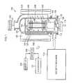
- FIG. 1is a schematic cross-sectional view showing an example of a film formation apparatus 100 according to a first embodiment of the present invention.
- the film formation apparatus 100includes a process chamber 101 having a shape of a bottom-open cylinder with ceiling.
- the entire process chamber 101may be formed of, for example, quartz.
- a ceiling plate 102 formed of quartzis provided on the ceiling of the process chamber 101 .
- a manifold 103which is formed of, for example, a stainless steel and has a cylinder, is connected to a bottom opening of the process chamber 101 via a sealing member 104 such as an O-ring.
- the manifold 103supports a bottom of the process chamber 101 .
- a wafer boat 105 formed of quartzis provided to be capable of inserting into the process chamber 101 from below the manifold 103 .
- the wafer boat 105can hold a plurality of, for example, 50 to 100, semiconductor substrates (n-type silicon substrates 1 doped with n-type impurities in the present embodiment) as object to be processed in a multi stage manner. Accordingly, in the process chamber 101 according to the present embodiment, the objects to be processed, each including an n-type silicon substrate (wafer) 1 on which an insulating film having an opening reaching the n-type silicon substrate 1 is formed, are held.
- the wafer boat 105includes a plurality of pillars 106 , and recesses provided in the pillars 106 support the plurality of n-type silicon substrates 1 .
- the wafer boat 105is placed on a table 108 via a thermos vessel 107 formed of quartz.
- the table 108is supported on a rotation shaft 110 that penetrates through a cover unit 109 that is formed of, for example, stainless steel, to open/close the bottom opening of the manifold 103 .
- a magnetic fluid seal 111is provided on a penetration portion of the rotation shaft 110 so as to rotatably support the rotation shaft 110 while sealing the rotation shaft 110 airtight.
- a sealing member 112 formed of, for example, an O-ring,is interposed between a circumferential portion of the cover unit 109 and the lower end portion of the manifold 103 . Accordingly, sealing in the process chamber 101 is maintained.
- the rotation shaft 110is attached to a leading end of an arm 113 supported by an elevating mechanism (not shown), for example, a boat elevator. Therefore, the wafer boat 105 , the cover unit 109 , and the like are integrally elevated to be inserted into or pulled out from the process chamber 101 .
- an elevating mechanismfor example, a boat elevator. Therefore, the wafer boat 105 , the cover unit 109 , and the like are integrally elevated to be inserted into or pulled out from the process chamber 101 .
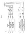
- the film formation apparatus 100includes a gas supply mechanism 114 for supplying a gas used to perform a process into the process chamber 101 .
- FIG. 2is a schematic block diagram showing an example of the gas supply mechanism 114 shown in FIG. 1 .
- the gas supply mechanism 114includes an inert gas supply source 115 for supplying an inert gas, a silane-based gas supply source 121 for supplying a silane-based gas not including an amino group, and an aminosilane-based gas supply source 122 for supplying an aminosilane-based gas.
- an inert gas supply source 115for supplying an inert gas
- a silane-based gas supply source 121for supplying a silane-based gas not including an amino group
- an aminosilane-based gas supply source 122for supplying an aminosilane-based gas.
- following gasesare prepared or ready to be generated as examples of the above gases.
- Inert gasnitrogen (N 2 ) gas
- silane-based gas not including an amino groupmonosilane (SiH 4 ) gas
- DIPASdiisopropylaminosilane
- a gas supply source included in the gas supply mechanism 114is connected to a plurality of distribution nozzles 125 .
- the silane-based gas supply source 121is connected to a distribution nozzle 125 d via a flow rate controller 123 f and an opening/closing valve 124 f
- the aminosilane-based gas supply source 122is connected to a distribution nozzle 125 e via a flow rate controller 123 g and an opening/closing valve 124 g.
- the inert gas supply source 115is connected to the distribution nozzles 125 d and 125 e , respectively, via a flow rate controller 123 h and opening/closing valves 126 d and 126 e .
- the inert gasis used as a diluting gas for diluting the silane-based gas not including an amino group and the aminosilane-based gas, a carrier gas, or a purge gas for purging inside the process chamber 101 .
- the inert gas supply source 115may be connected to a gas introducing port (not shown) that is separately provided from the distribution nozzles 125 d and 125 e .
- the gas introducing port(not shown) may be provided, for example, to penetrate inward through a side wall of the manifold 103 .
- the gas introducing porthas a gas ejecting hole that is greater than that of the distribution nozzle 125 d or 125 e , and supplies the inert gas into the process chamber 101 from a lower portion of the process chamber 101 to a height-wise direction of the process chamber 101 via the inner side of the manifold 103 .
- Each of the plurality of distribution nozzles 125(in the present embodiment, the distribution nozzles 125 d and 125 e ) is formed of a quartz tube, and penetrates through a side wall of the manifold 103 into the manifold 103 and then bends upward.
- each of the distribution nozzlesis extended into the process chamber 101 in a vertical direction as shown in FIG. 1 .
- a plurality of gas ejecting holes 127are provided at predetermined intervals. The gases are uniformly ejected into the process chamber 101 from each of the gas ejecting holes 127 to a horizontal direction.
- An exhaust port 129 for evacuating the process chamber 101is provided in an opposite to the distribution nozzles 125 in the process chamber 101 .
- the exhaust port 129is provided to be narrow and long by vertically cutting the sidewall of the process chamber 101 .
- the exhaust port cover unit 130 having a U-shaped cross-section for covering the exhaust port 129is attached to a portion of the process chamber 101 corresponding to the exhaust port 129 by a welding process.
- the exhaust port cover unit 130extends upward along the sidewall of the process chamber 101 , and defines a gas outlet 131 on a top of the process chamber 101 .
- An exhauster 132 including a vacuum pump or the likeis connected to the gas outlet 131 .
- the exhauster 132evacuates an inside of the process chamber 101 to exhaust a process gas used in a process and set the pressure inside the process chamber 101 to be a process pressure according to a process.
- a barrel-shaped heating device 133is disposed to surround the outer circumference of the process chamber 101 .
- the heating device 133activates a gas supplied into the process chamber 101 , and at the same time, heats the object to be processed in the process chamber 101 , for example, the semiconductor substrates, that is, the n-type silicon substrates 1 in the present embodiment.
- controller 150that is, for example, a micro-processor (computer).
- a user interface 151 including a keyboard that receives an input operation of a command or the like for an operator to control the film formation apparatus 100 or a display that visibly displays an operating state of the film formation apparatus 100is connected to the controller 150 .
- a memory unit 152is connected to the controller 150 .
- the memory unit 152stores a control program for accomplishing various processes executed in the film formation apparatus 100 under the control of the controller 150 , or a program, that is, a recipe, for making each of components of the film formation apparatus 100 execute a process according to process conditions.
- the recipeis stored in a storage medium in the memory unit 152 , for example.
- the storage mediummay be a hard disk, a semiconductor memory, or a portable type such as a CD-ROM, a DVD, or a flash memory.
- the recipemay be suitably transmitted from another device via, for example, a dedicated line.
- processes desired by the film formation apparatus 100are performed under the control of the controller 150 by invoking a recipe from the memory unit 152 according to instructions or the like from the user interface 151 .
- a film formation methodthat will be described as follows is sequentially performed in one process chamber 101 under the control of the controller 150 .
- FIGS. 3A through 3Care cross-sectional views showing an example of a film formation method executable by a film formation apparatus according to a first embodiment of the present invention.
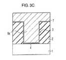
- FIG. 3Ais a cross-sectional view illustrating that a contact hole 3 reaching a n-type silicon substrate 1 is provided on an interlayer insulation film 2 formed on the n-type silicon substrate 1 .
- a thin natural oxide film 4is grown on a surface of the n-type silicon substrate 1 exposed on a bottom of the contact hole 3 .
- the natural oxide film 4causes a contact resistance to increase.
- the natural oxide film 4may be removed.
- the natural oxide film 4may not be necessarily removed. In the present embodiment, the natural oxide film 4 is not removed.
- the n-type silicon substrate 1 on which the natural oxide film 4 is grownis transferred into the process chamber 101 of the film formation apparatus 100 shown in FIG. 1 .
- the heating apparatus 133heats an inside of the process chamber 101 to a predetermined temperature.
- a temperature inside the process chamber 101is adjusted such that a temperature of the n-type silicon substrate 1 is about 300° C. to 550° C., for example.
- the opening/closing valves 124 g and 126 eare opened so as to supply the nitrogen (N 2 ) gas and the diisopropylaminosilane (DIPAS) gas into the process chamber 101 respectively from the inert gas supply source 115 and the aminosilane-based gas supply source 122 via the distribution nozzle 125 e .
- N 2nitrogen
- DIPASdiisopropylaminosilane
- FIG. 3Ba seed layer 7 is formed on a surface of the interlayer insulation film 2 and the bottom surface of the contact hole 3 .
- the opening/closing valve 124 gis closed to stop the supply of the DIPAS gas, and at the same time, an atmosphere inside the process chamber 101 is purged by using the N 2 gas.
- the exhauster 132is stopped and the opening/closing valve 126 e is closed to stop the supply of the N 2 gas.
- the temperature inside the process chamber 101is adjusted such that the temperature of the n-type silicon substrate 1 is about 400° C. to 650° C., for example.
- the opening/closing valves 124 f and 126 dare opened so as to supply the N 2 gas and the monosilane (SiH 4 ) gas into the process chamber 101 from the inert gas supply source 115 and the silane-based gas supply source 121 via the distribution nozzle 125 d .
- a silicon filmthat is, an amorphous silicon film 8 a in the present embodiment, is formed on the seed layer 7 , to thereby fill the contact hole 3 .
- the opening/closing valve 124 fis closed to stop the supply of the SiH 4 gas, and at the same time, the atmosphere inside the process chamber 101 is purged by using the N 2 gas. After that, the exhauster 132 is stopped and the opening/closing valve 126 d is closed to stop the supply of the N 2 gas.
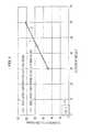
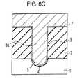
- FIG. 4is a diagram illustrating a relationship between deposition times and thicknesses of the amorphous silicon film 8 a .
- FIG. 4shows results for a case where a base is a silicon oxide film (SiO 2 ).
- the basecorresponds to the interlayer insulation film 2 in the present embodiment.
- the followingsare process conditions for forming the amorphous silicon film 8 a of the present embodiment.
- the thicknesses of the amorphous silicon film 8 awere measured respectively when the deposition times were 30 minutes, 45 minutes, and 60 minutes.
- a line Idenotes a result when the seed layer 7 is formed
- a line IIdenotes a result when the seed layer 7 is not formed.
- the lines I and IIare approximation lines obtained from the three measurements of the thickness by using the method of least squares and expressions thereof are following Equations (1) and (2).
- Line I: y17.572 ⁇ 20.855
- Line II: y17.605 ⁇ 34.929 (2)
- FIG. 5is an enlarged view of a portion A of FIG. 4 indicated by the broken line.
- a deposition of the amorphous silicon film 8 astarts at about 1.2 minutes (x ⁇ 1.189) after initiating the process.
- a deposition of the amorphous silicon film 8 astarts at about 2 minutes (x ⁇ 1.984) after initiating the process.
- an incubation timemay be reduced from about 2 minutes to about 1.2 minutes.
- filling of the contact hole 3is performed by forming the seed layer 7 on the surface of the interlayer insulation film 2 and the bottom surface of the contact hole 3 by using the aminosilane-based gas, and forming the silicon film, that is, the amorphous silicon film 8 a in the present embodiment, on the seed layer 7 by using the silane-based gas that does not include the amino group.
- the incubation time of the amorphous silicon film 8 amay be reduced less than that of a case where the seed layer 7 is not formed.
- the film formation apparatus 100 having excellent production capabilitymay be provided even when filling processes are frequently performed in the semiconductor integrated circuit device.
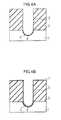
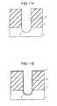
- FIGS. 6A through 6Care cross-sectional views showing modified examples of the film formation method executable by the film forming apparatus according to the first embodiment of the present invention.
- the contact hole 3Since the contact hole 3 is miniaturized, the diameter D of the contact hole 3 is reduced as shown in FIG. 6A , a surface area of the contact portion is reduced, and thus the contact resistance is increased. To address the problem of the increased contact resistance, as denoted by reference numeral 5 in FIG. 6A , the bottom of the contact hole 3 may be recessed to increase the surface area of the contact portion.
- the first embodiment of the present inventionmay be applied as shown in FIGS. 6A through 6C even in the semiconductor integrated circuit device having the contact hole 3 , the bottom of which is recessed.
- FIG. 7is a block diagram showing an example of a gas supply mechanism included in a film formation apparatus according to a second embodiment of the present invention.
- the gas supply mechanism 114 included in the film formation apparatus according to the present embodimentis different from the gas supply mechanism 114 of the film formation apparatus according to the first embodiment in that a gas supply source that supplies a gas for removing a natural oxide film is additionally provided.
- a first gas supply source 116that supplies a first gas for removing the natural oxide film
- a second gas supply source 117that supplies a second gas for removing the natural oxide film are provided.
- the following gasesare prepared or configured to be generated as examples of the above first and second gases.
- the first gas supply source 116is connected to a distribution nozzle 125 a via a flow rate controller 123 a and an opening/closing valve 124 a .
- the second gas supply source 117is connected to a distribution nozzle 125 b via a flow rate controller 123 b and an opening/closing valve 124 b.
- Each of the distribution nozzles 125 a and 125 bis formed of a quartz tube like the other distribution nozzles, and penetrates through a side wall of the manifold 103 into the manifold 103 and then bends upward.
- each of the distribution nozzles 125 a and 125 bis extended into the process chamber 101 in a vertical direction.
- FIGS. 8A through 8Dare cross-sectional views showing an example of a film formation method executable by the film formation apparatus 100 according to the second embodiment of the present invention.
- an n-type silicon substrate 1 on which the natural oxide film 4 is grownis transferred into a process chamber 101 of the film formation apparatus 100 .
- the heating apparatus 133heats the process chamber 101 to a predetermined temperature.
- a temperature inside the process chamber 101is adjusted such that a temperature of the n-type silicon substrate 1 is about 20° C. to 300° C.
- the opening/closing valves 124 a and 124 bare closed to stop the supplies of the NH 3 gas and the HF gas.
- the process chamber 101is evacuated by the exhauster 132 so as to supply the N 2 gas into the process chamber 101 and to purge an atmosphere inside the process chamber 101 by using the N 2 gas. After that, the exhauster 132 is stopped and the opening/closing valves 126 a and 126 b are closed to stop the supply of the N 2 gas.
- the seed layer 7 and the amorphous silicon film 8 aare formed according to the film formation method described with reference to FIGS. 3B and 3C .
- the filling process of the contact hole 3is performed in the same manner as that of the first embodiment, and thus, the incubation time of the amorphous silicon film 8 a filling the contact hole 3 may be reduced, and the throughput of the filling process may be improved. Therefore, like the previous embodiment, the film formation apparatus 100 having an excellent production capability with respect to the semiconductor integrated circuit device in which the filling processes are frequently performed may be obtained.
- the natural oxide film 4may be removed, and thus, an increase in the contact resistance may be prevented.
- the natural oxide film 4is removed in the process chamber of the film formation apparatus, in which forming of the amorphous silicon film 8 a is performed. Therefore, the forming of the amorphous silicon film 8 a may be performed rapidly after removing the natural oxide film 4 . Accordingly, deterioration of the throughput in the filling process caused by the removal of the natural oxide film 4 may be prevented.
- FIG. 9is a schematic block diagram showing an example of a gas supply mechanism included in a film formation apparatus according to a third embodiment of the present invention.
- the gas supply mechanism 114 included in the film formation apparatus according to the third embodiment of the present inventionis different from the gas supply mechanism 114 in the film formation apparatus according to the second embodiment in that a dopant gas supply source 120 that supplies a gas including a dopant is additionally provided.
- n-type impuritiesthat have the same conductive type as the n-type silicon substrate 1 is used as the dopant.
- the dopant gas supply source 120prepares or generates the following gas including the n-type impurities.
- dopant gasphosphine (PH 3 ) gas
- the dopant gas supply source 120is connected to a distribution nozzle 125 d via a flow rate controller 123 e and an opening/closing valve 124 e.
- FIGS. 10A through 10Care cross-sectional views showing an example of a film formation method executable by the film formation apparatus according to the third embodiment of the present invention.
- the natural oxide film 4 on the surface of the n-type silicon substrate 1 that is exposed on the bottom of the contact hole 3is removed according to the film formation method described in the second embodiment.
- the temperature inside the process chamber 101is adjusted such that the temperature of the n-type silicon substrate 1 is about 400° C. to 650° C., for example.
- the opening/closing valves 124 e and 126 dare opened so as to supply the N 2 gas and the phosphine (PH 3 ) gas into the process chamber 101 from the inert gas supply source 115 and the dopant gas supply source 120 via the distribution nozzle 125 d.
- n-type impuritiesthat is, phosphorous (P)
- Pphosphorous
- the seed layer 7 and the amorphous silicon film 8 aare formed according to the film formation method described with reference to FIGS. 3B and 3C .
- the filling process of the contact hole 3is performed in the same manner as that of the first embodiment. Therefore, like the first embodiment, the film formation apparatus 100 having an excellent production capability with respect to the semiconductor integrated circuit device in which the filling processes are frequently performed may be obtained.
- the n-type impuritiesmay be introduced onto the surface of the n-type silicon substrate 1 located on the bottom of the contact hole 3 . Therefore, the concentration of the n-type impurities on the n-type silicon substrate 1 located on the bottom of the contact hole 3 may be increased, and thus, the contact resistance may be reduced.
- introducing of the n-type impuritiesis performed in the process chamber of the film formation apparatus 100 , in which the amorphous silicon film 8 a is formed. Therefore, the forming of the amorphous silicon film 8 a may be performed rapidly after introducing the n-type impurities. Accordingly, when the n-type impurities are introduced, deterioration of the throughput in the filling process may be prevented.
- FIGS. 11A through 11Care cross-sectional views showing a modified example of the film formation method executable by the film formation apparatus according to the third embodiment of the present invention.
- the n-type impuritiesare introduced onto the n-type silicon substrate 1 ; however, the n-type impurities may be introduced onto the amorphous silicon film 8 a.
- the seed layer 7is formed according to the film formation method described with reference to FIGS. 8B and 8C , and after that, the opening/closing valves 124 e , 126 d , and 124 f are opened so as to supply the N 2 gas, the PH 3 gas, and the monosilane gas into the process chamber 101 from the inert gas supply source 115 , the dopant gas supply source 120 , and the silane-based gas supply source 121 via the distribution nozzle 125 d .
- the opening/closing valves 124 e , 126 d , and 124 fare opened so as to supply the N 2 gas, the PH 3 gas, and the monosilane gas into the process chamber 101 from the inert gas supply source 115 , the dopant gas supply source 120 , and the silane-based gas supply source 121 via the distribution nozzle 125 d .
- the concentration of the n-type impurities in the doped amorphous silicon film 8 a *is greater than that of the n-type silicon substrate 1 , the n-type impurities are dispersed toward the n-type silicon substrate 1 from the doped amorphous silicon film 8 a *, for example, as shown in FIG. 11C .
- the n-type impuritiesmay be introduced onto the amorphous silicon film 8 a to form the doped amorphous silicon film 8 a *.
- the doped amorphous silicon film 8 a *has less resistance, and the contact resistance may be reduced.
- the n-type impurities in the doped amorphous silicon film 8 a *is higher than that of the n-type silicon substrate 1 , the n-type impurities are dispersed toward the n-type silicon substrate 1 from the doped amorphous silicon film 8 a *, for example, as shown in FIG. 11C . Through the dispersion, the contact resistance on the n-type silicon substrate 1 may be reduced.
- the n-type impuritiesmay be introduced onto the contact portion of the n-type silicon substrate as described with reference to FIG. 10A , and the doped amorphous silicon film 8 a * may be additionally formed according to the film formation method described with reference to FIG. 11C .
- FIG. 12is a schematic block diagram showing an example of a gas supply mechanism 114 included in a film formation apparatus according to a fourth embodiment of the present invention.
- the gas supply mechanism 114 included in the film formation apparatus according to the fourth embodimentis different from the gas supply mechanism 114 included in the film formation apparatus according to the third embodiment in that a third gas supply source 119 for supplying a gas etching silicon film is additionally provided.
- the third gas supply source 119may prepare or generate the following gas for etching the silicon film in the present embodiment.
- the third gas supply source 119is connected to a distribution nozzle 125 c via a flow rate controller 123 d and an opening/closing valve 124 d.
- the distribution nozzle 125 cis formed of a quartz tube, and penetrates through the side wall of the manifold 103 into the manifold 103 and then bends upward. In addition, the distribution nozzle 125 c is extended into the process chamber 101 in a vertical direction, as shown in FIG. 1 .
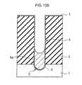
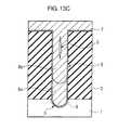
- FIGS. 13A through 13Eare cross-sectional views showing an example of the film formation method executable by the film formation apparatus according to the fourth embodiment of the present invention.
- the filling of the contact hole 3may be finished.
- an aspect ratio of the contact hole 3is high (when the contact hole 3 is narrow and long in a longitudinal direction)
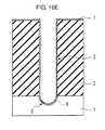
- a void 9may be provided on the amorphous silicon film 8 a as shown in FIG. 13A .
- the following additional processesare performed under the assumption that the void 9 is provided on the amorphous silicon film 8 a.
- the temperature inside the process chamber 101is adjusted such that the temperature of the n-type silicon substrate 1 is about 200° C. to 500° C., for example.
- the opening/closing valves 124 d and 126 care opened so as to supply the N 2 gas and the Cl 2 gas into the process chamber 101 from the inert gas supply source 115 and the third gas supply source 119 via the distribution nozzle 125 c .
- a region of the amorphous silicon film 8 a reaching an intermediate portion of the contact hole 3for example, a region of the amorphous silicon film 8 a in which the void 9 is assumed to be provided, is removed, as shown in FIG. 13B .
- the opening/closing valve 124 dis closed to stop the supply of the Cl 2 gas, and at the same time, the atmosphere inside the process chamber 101 is purged by using the N 2 gas. After that, the exhauster 132 is stopped and the opening/closing valve 126 c is closed to stop the supply of the N 2 gas.
- the temperature inside the process chamber 101is adjusted such that the temperature of the n-type silicon substrate 1 is about 400° C. to 650° C., for example.
- the opening/closing valves 124 f and 126 dare opened so as to supply the N 2 gas and the SiH 4 gas into the process chamber 101 from the inert gas supply source 115 and the silane-based gas supply source 121 via the distribution nozzle 125 d .
- a silicon filmthat is, an amorphous silicon film 8 b in the present embodiment, is formed on the seed layer 7 and the amorphous silicon film 8 a , and thus the contact hole 3 is filled again as shown in FIG. 13C .
- the opening/closing valve 124 fis closed to stop the supply of the SiH 4 gas, and the atmosphere inside the process chamber 101 is purged by using the N 2 gas. After that, the exhauster 132 is stopped and the opening/closing valve 126 d is closed to stop the supply of the N 2 gas is stopped.
- the deposition and etching operationsare repeated, for example, as shown in FIGS. 13D and 13E , and thus the contact hole 3 is filled by the amorphous silicon films 8 a and 8 b and an amorphous silicon film 8 c while removing regions, in which the void 9 is assumed to be provided, from the amorphous silicon films 8 a and 8 b .
- the final amorphous silicon filmthat is, the amorphous silicon film 8 c in the present embodiment as a third layer, is formed, the n-type silicon substrate 1 is transferred from the process chamber 101 .
- the initial step of the filling process of the contact hole 3that is, forming of the amorphous silicon film 8 a , is performed in the same manner as that of the first embodiment. Therefore, the same effects as those of the first embodiment may be obtained.
- the void 9 provided in the amorphous silicon films 8 a and 8 bmay be removed, and thus, the increase in the contact resistance caused due to the providing of the void 9 may be prevented.
- the forming and etching of the amorphous silicon films 8 a and 8 bmay be performed in the same process chamber of the film formation apparatus, and thus, there is no need to transfer substrates between devices to perform the film formation and etching processes. Therefore, deterioration of the throughput may be prevented.
- the above described first embodimentis mainly to improve the throughput in the filling process by reducing the incubation time of the formed film.
- the second through fourth embodimentsare to prevent the increase in the contact resistance in the contact hole or the line that is miniaturized, as well as to improve the throughput.
- contact resistanceincreases because, for example,
- the fifth embodimentis to provide a film formation apparatus that may address the above problems 1) through 3) with one film formation apparatus, and may improve the throughput by reducing the incubation time of the formed film.
- FIG. 14is a schematic block diagram showing an example of a gas supply mechanism included in the film formation apparatus according to the fifth embodiment of the present invention.
- the gas supply mechanism 114 included in the film formation apparatus according to the fifth embodimentis different from the gas supply mechanism 114 included in the film formation apparatus according to the fourth embodiment in that a fourth gas supply source 118 for supplying a fourth gas that may etch a conductive substance, that is, the n-type silicon substrate 1 in the present embodiment, is additionally provided in the present embodiment.
- the fourth gas supply source 118may prepare or generate the following gas that may etch a conductive substance.
- the fourth gas supply source 118is connected to the distribution nozzle 125 c via the flow rate controller 123 c and the opening/closing valve 124 c.
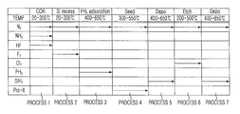
- FIG. 15is a timing chart showing examples of supply of process gases and process temperatures in a film formation method executable by a film formation apparatus according to fifth embodiment of the present invention
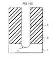
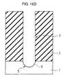
- FIGS. 16A through 16Jare cross-sectional views showing the film formation method.
- FIG. 16Ais a cross-sectional view showing that the contact hole 3 reaching the n-type silicon substrate 1 is provided on the interlayer insulation film 2 formed on the n-type silicon substrate 1 .
- a thin natural oxide film 4is grown on a surface of the n-type silicon substrate 1 exposed on a bottom of the contact hole 3 .
- the n-type silicon substrate 1 on which the natural oxide film 4 is grownis transferred to the process chamber 101 of the film formation apparatus 100 shown in FIG. 1 .
- the heating apparatus 133heats the process chamber 101 to a predetermined temperature.
- a temperature inside the process chamber 101is adjusted such that a temperature of the n-type silicon substrate 1 is about 20° C. to 300° C.
- the opening/closing valves 124 a and 124 bare closed to stop the supplies of the NH 3 gas and the HF gas.
- N 2 gasis supplied into the process chamber 101 to purge an atmosphere inside the process chamber 101 by using the N 2 gas.
- the exhauster 132is stopped and the opening/closing valves 126 a and 126 b are closed to stop the supply of the N 2 gas.
- the temperature inside the process chamber 101is adjusted such that the temperature of the n-type silicon substrate 1 is about 20° C. to 300° C., for example.
- the opening/closing valves 124 c and 126 care opened so as to supply the N 2 gas and the fluorine (F 2 ) gas into the process chamber 101 from the inert gas supply source 115 and the fourth gas supply source 118 via the distribution nozzle 125 c (process 2: Si recess shown in FIG. 15 ).
- process 2Si recess shown in FIG. 15
- the surface of the n-type silicon substrate 1 exposed on the bottom of the contact hole 3is recessed as denoted by reference numeral 5 , as shown in FIG. 16C .
- the opening/closing valve 124 cis closed to stop the supply of the F 2 gas, and at the same time, the atmosphere inside the process chamber 101 is purged by using the N 2 gas. After that, the exhauster 132 is stopped and the opening/closing valve 126 c is closed to stop the supply of the N 2 gas.
- the temperature inside the process chamber 101is adjusted such that the temperature of the n-type silicon substrate 1 is about 400° C. to 650° C., for example.
- the opening/closing valves 124 e and 126 dare opened so as to supply the N 2 gas and the phosphine (PH 3 ) gas into the process chamber 101 from the inert gas supply source 115 and the dopant gas supply source 120 via the distribution nozzle 125 d (process 3: PH 3 adsorption shown in FIG. 15 ).
- n-type impuritiesthat is, phosphorous (P)
- Pphosphorous
- the temperature inside the process chamber 101is adjusted such that the temperature of the n-type silicon substrate 1 is about 300° C. to 550° C., for example.
- the opening/closing valves 124 g and 126 eare opened so as to supply the N 2 gas and the diisopropylaminosilane (DIPAS) gas (represented as Pre-X in FIG. 15 ) into the process chamber 101 from the inert gas supply source 115 and the aminosilane-based gas supply source 122 via the distribution nozzle 125 e (process 4: Seed shown in FIG. 15 ).
- DIPASdiisopropylaminosilane
- a seed layer 7is formed on the interlayer insulation film 2 and the recessed surface of the n-type silicon substrate 1 as shown in FIG. 16E .
- the opening/closing valve 124 gis closed to stop the supply of the DIPAS gas, and at the same time, the atmosphere inside the process chamber 101 is purged by using the N 2 gas.
- the exhauster 132is stopped and the opening/closing valve 126 e is closed to stop the supply of the N 2 gas.
- the temperature inside the process chamber 101is adjusted such that the temperature of the n-type silicon substrate 1 is about 400° C. to 650° C., for example.
- the opening/closing valves 124 f and 126 dare opened so as to supply the N 2 gas and the monosilane (SiH 4 ) gas into the process chamber 101 from the inert gas supply source 115 and the silane-based gas supply source 121 via the distribution nozzle 125 d (process 5: Depo shown in FIG. 15 ).
- a silicon filmthat is, an amorphous silicon film 8 a in the present embodiment, is formed on the seed layer 7 to fill the contact hole 3 , as shown in FIG. 16F .
- the opening/closing valve 124 fis closed to stop the supply of the SiH 4 gas, and at the same time, the atmosphere inside the process chamber 101 is purged by using the N 2 gas. After that, the exhauster 132 is stopped and the opening/closing valve 126 d is closed to stop the supply of the N 2 gas.
- a dopantmay be introduced onto the amorphous silicon film 8 a from the dopant gas supply source 120 via the distribution nozzle 125 d so as to form the doped amorphous silicon film 8 a *, like in the modified example of the third embodiment.
- the filling of the contact hole 3may be finished at a stage where the amorphous silicon film 8 a is formed.
- the film formation and etching operationsare repeated, and thus the film may be formed while removing regions in which the void 9 is assumed to be provided, from the amorphous silicon film 8 a .
- the following additional processesare performed under the assumption that the void 9 is provided in the present embodiment.
- the temperature inside the process chamber 101is adjusted such that the temperature of the n-type silicon substrate 1 is about 200° C. to 500° C., for example.
- the opening/closing valves 124 d and 126 care opened so as to supply the N 2 gas and the chlorine (Cl 2 ) gas into the process chamber 101 from the inert gas supply source 115 and the third gas supply source 119 via the distribution nozzle 125 c (process 6: Etch shown in FIG. 15 ).
- a region of the amorphous silicon film 8 a reaching an intermediate portion of the contact hole 3for example, a region of the amorphous silicon film 8 a in which the void 9 is assumed to be provided, is removed.
- the opening/closing valve 124 dis closed to stop the supply of the Cl 2 gas, and at the same time, the atmosphere inside the process chamber 101 is purged by using the N 2 gas.
- the exhauster 132is stopped and the opening/closing valve 126 c is closed to stop the supply of the N 2 gas.
- the temperature inside the process chamber 101is adjusted such that the temperature of the n-type silicon substrate 1 is about 400° C. to 650° C., for example.
- the opening/closing valves 124 f and 126 dare opened so as to supply the N 2 gas and the SiH 4 gas into the process chamber 101 from the inert gas supply source 115 and the silane-based gas supply source 121 via the distribution nozzle 125 d (process 7: Depo shown in FIG. 15 ).
- a silicon filmthat is, an amorphous silicon film 8 b in the present embodiment, is formed on the seed layer 7 and the amorphous silicon film 8 a , and thus the contact hole 3 is filled again, as shown in FIG. 16H .
- the opening/closing valve 124 fis closed to stop the supply of the SiH 4 gas, and at the same time, the atmosphere inside the process chamber 101 is purged by using the N 2 gas. After that, the exhauster 132 is stopped and the opening/closing valve 126 d is closed, and then the supply of the N 2 gas is stopped.
- the deposition and etching operationsare repeated, for example, as shown in FIGS. 16I and 16J , and thus the contact hole 3 is filled by the amorphous silicon films 8 a and 8 b and an amorphous silicon film 8 c while removing regions in which the void 9 is assumed to be provided, from the amorphous silicon films 8 a and 8 b .
- the final amorphous silicon filmthat is, the amorphous silicon film 8 c in the present embodiment, is formed as a third layer, the n-type silicon substrate 1 is transferred from the process chamber 101 .
- the amorphous silicon films 8 b and 8 cmay be formed as doped amorphous silicon films.
- the film formation method using the film formation apparatus according to the fifth embodimentthat is, the filling process of the contact hole 3 , is finished.
- the natural oxide film 4is removed from the surface of the n-type silicon substrate 1 exposed on the bottom of the contact hole 3 .
- an increase in contact resistance caused by the natural oxide film 4may be prevented.
- the surface of the n-type silicon substrate 1 exposed on the bottom of the contact hole 3is recessed.
- a surface area of a contact portionis greater than that in a case where the exposed surface of the n-type silicon substrate 1 is not recessed, and thus an increase in the contact resistance caused by a reduced surface area of the contact portion may be prevented.
- the seed layer 7is formed by using the aminosilane-based gas in the process 4.
- the incubation time of the amorphous silicon film 8 a formed by using the silane-based gas in the process 5may be reduced.
- the above advantages (1) through (3)may be obtained by performing the method using only one film formation apparatus 100 .
- the deposition and etching of the amorphous silicon filmare repeated, and then the void provided in the deposited amorphous silicon film is removed.
- the volume reduction of the amorphous silicon film filled in the contact hole 3 caused by the voidmay be prevented, and thus an increase in the contact resistance caused by the volume reduction may be prevented.
- the n-type impuritiesthat is, phosphorous (P)
- the n-type impuritiesis adsorbed onto the recessed surface of the n-type silicon substrate 1 . Accordingly, the concentration of the n-type impurities on the surface portion of the n-type silicon substrate 1 may be increased, and thus, the resistance on the surface of the n-type silicon substrate 1 may be reduced.
- the above advantages (4) and (5)may be also obtained by performing the method using only one film formation apparatus 100 , with the advantages (1) through (3).
- the film formationmay prevent or reduce the increase in the contact resistance even in the contact hole that is miniaturized, and the incubation time of the formed film is short and thus a film formation apparatus that may improve a throughput is provided.
- the amorphous silicon film 8 bis formed by using the silane-based gas not including an amino group in the process 7.
- the amorphous silicon film 8 ais removed to an intermediate portion of the contact hole 3 , and after that, the aminosilane-based gas is supplied into the process chamber 101 again so that a new seed layer is formed on the interlayer insulation film 2 and the surface of the amorphous silicon film 8 a . After that, the silane-based gas not including an amino group is supplied into the process chamber 101 again so that the amorphous silicon film 8 b may be formed on the new seed layer.
- the film formation apparatus 100is applied to the filling process of the contact hole 3 reaching the n-type silicon substrate 1 .
- the present inventionis not limited to the filling process of the contact hole 3 , and may be applied to a filling process of recessed lines with the above advantages.
- the contact hole 3may reach a p-type silicon substrate, or an active region such as a source region or a drain region provided on the n-type or p-type silicon substrate, or a well, as well as the n-type silicon substrate 1 .
- the contact hole 3may reach a metal wire such as copper, as well as a semiconductor region.
- the DIPAS gasis used as the aminosilane-based gas; however, following aminosilane-based gases in addition to the DIPAS gas may be used as the aminosilane-based gas.
- BBASBistertiarybutylaminosilane
- DMASDimethylaminosilane
- DPASDipropylaminosilane
- the monosilane gas (SiH 4 ) gasis used as the silane-based gas not including an amino group; however, following silane-based gases that do not include an amino-group may be used besides the SiH 4 gas.
- a hydride of siliconrepresented by Si m H 2m+2 , where m is a natural number equal to 3 or greater, and
- a hydride of siliconrepresented by Si n H 2n , where n is a natural number equal to 3 or greater.
- the hydride of silicon represented by the Si m H 2m+2may be at least one of:
- the hydride of silicon represented by the Si n H 2nmay be at least one of:
- componentsmay be omitted in the third through fifth embodiments.
- first gas supply source 116 and the second gas supply source 117may be omitted from the gas supply mechanism 114 shown in FIG. 9 according to the third embodiment.
- At least one of the first gas supply source 116 , the second gas supply source 117 , and the dopant gas supply source 120may be omitted from the gas supply mechanism 114 shown in FIG. 12 according to the fourth embodiment.
- At least one of the first gas supply source 116 , the second gas supply source 117 , the third gas supply source 119 , and the dopant gas supply source 120may be omitted from the gas supply mechanism 114 shown in FIG. 14 according to the fifth embodiment.
- the film formation apparatussince the throughput of the filling process may be improved, the film formation apparatus has an excellent production capability with respect to the semiconductor integrated circuit device in which the filling processes are frequently used.
Landscapes
- Engineering & Computer Science (AREA)
- Chemical & Material Sciences (AREA)
- Physics & Mathematics (AREA)
- Condensed Matter Physics & Semiconductors (AREA)
- General Physics & Mathematics (AREA)
- Manufacturing & Machinery (AREA)
- Computer Hardware Design (AREA)
- Microelectronics & Electronic Packaging (AREA)
- Power Engineering (AREA)
- General Chemical & Material Sciences (AREA)
- Chemical Kinetics & Catalysis (AREA)
- Materials Engineering (AREA)
- Mechanical Engineering (AREA)
- Metallurgy (AREA)
- Organic Chemistry (AREA)
- Inorganic Chemistry (AREA)
- Plasma & Fusion (AREA)
- Electrodes Of Semiconductors (AREA)
- Chemical Vapour Deposition (AREA)
- Internal Circuitry In Semiconductor Integrated Circuit Devices (AREA)
Abstract
Description
This application claims the benefits of Japanese Patent Application No. 2010-243130, filed on Oct. 29, 2010 and Japanese Patent Application No. 2011-207962, filed on Sep. 22, 2011, in the Japan Patent Office, the disclosures of which are incorporated herein in its entirety by reference.
1. Field of the Invention
The present invention relates to a film formation apparatus.
2. Description of the Related Art
Amorphous silicon is used to fill a contact hole or a line in a semiconductor integrated circuit device. A method of forming an amorphous silicon film is disclosed in, for example,Patent reference 1.
Recently, along with miniaturization of semiconductor integrated circuit devices, filling of contact holes or lines has become strictly required.
In addition, in the field of semiconductor manufacturing apparatuses, improvement in production capacity is particularly considered as being important, as well as establishment of production technology according to the miniaturization. Semiconductor integrated circuit devices now have multiple wiring structures along with the miniaturization, and moreover, semiconductor integrated circuit devices are desired to have three-dimensional structures. In the semiconductor integrated circuit devices having the multiple wiring structures or the three-dimensional structures, filling processes are frequently used. In order to further improve the production capacity, it is a top priority to improve a throughput of the filling process.
3. Prior Art Reference
- (Patent Reference 1) Japanese Patent Laid-open Publication No. sho 63-29954
The present invention provides a film formation apparatus capable of producing semiconductor integrated circuit devices, in which filling processes are frequently performed, with a high production capability by improving a throughput of the filling processes.
According to an aspect of the present invention, a film formation apparatus used to fill an opening provided on an insulation film, the opening reaching a conductive substance, the film formation apparatus includes: a process chamber which holds an object to be processed having the insulation film provided on the conductive substance, the insulation film having the opening reaching the conductive substance; and a gas supply mechanism which is provided in the process chamber and supplies an aminosilane-based gas, and a silane-based gas that does not include an amino group, wherein processes of 1) forming a seed layer on a surface of the insulation film having the opening reaching the conductive substance and on a bottom surface of the opening by supplying the aminosilane-based gas into the process chamber, and 2) forming a silicon film on the seed layer by supplying the silane-based gas that does not include the amino group into the process chamber, may be sequentially performed in the process chamber.
Additional objects and advantages of the invention will be set forth in the description which follows, and in part will be obvious from the description, or may be learned by practice of the invention.
The objects and advantages of the invention may be realized and obtained by means of the instrumentalities and combinations particularly pointed out hereinafter.
The accompanying drawings, which are incorporated in and constitute a part of the specification, illustrate embodiments of the invention, and together with the general description given above and the detailed description of the embodiments given below, serve to explain the principles of the invention.
An embodiment of the present invention achieved on the basis of the findings given above will now be described with reference to the accompanying drawings. In the following description, the constituent elements having substantially the same function and arrangement are denoted by the same reference numerals, and a repetitive description will be made only when necessary.
As shown inFIG. 1 , thefilm formation apparatus 100 includes aprocess chamber 101 having a shape of a bottom-open cylinder with ceiling. Theentire process chamber 101 may be formed of, for example, quartz. Aceiling plate 102 formed of quartz is provided on the ceiling of theprocess chamber 101. Amanifold 103, which is formed of, for example, a stainless steel and has a cylinder, is connected to a bottom opening of theprocess chamber 101 via a sealingmember 104 such as an O-ring.
Themanifold 103 supports a bottom of theprocess chamber 101. Awafer boat 105 formed of quartz is provided to be capable of inserting into theprocess chamber 101 from below themanifold 103. Thewafer boat 105 can hold a plurality of, for example, 50 to 100, semiconductor substrates (n-type silicon substrates 1 doped with n-type impurities in the present embodiment) as object to be processed in a multi stage manner. Accordingly, in theprocess chamber 101 according to the present embodiment, the objects to be processed, each including an n-type silicon substrate (wafer)1 on which an insulating film having an opening reaching the n-type silicon substrate 1 is formed, are held. Thewafer boat 105 includes a plurality ofpillars 106, and recesses provided in thepillars 106 support the plurality of n-type silicon substrates 1.
Thewafer boat 105 is placed on a table108 via athermos vessel 107 formed of quartz. The table108 is supported on arotation shaft 110 that penetrates through acover unit 109 that is formed of, for example, stainless steel, to open/close the bottom opening of themanifold 103. A magnetic fluid seal111, for example, is provided on a penetration portion of therotation shaft 110 so as to rotatably support therotation shaft 110 while sealing therotation shaft 110 airtight. A sealingmember 112 formed of, for example, an O-ring, is interposed between a circumferential portion of thecover unit 109 and the lower end portion of themanifold 103. Accordingly, sealing in theprocess chamber 101 is maintained. Therotation shaft 110 is attached to a leading end of an arm113 supported by an elevating mechanism (not shown), for example, a boat elevator. Therefore, thewafer boat 105, thecover unit 109, and the like are integrally elevated to be inserted into or pulled out from theprocess chamber 101.
Thefilm formation apparatus 100 includes agas supply mechanism 114 for supplying a gas used to perform a process into theprocess chamber 101.
Thegas supply mechanism 114 according to the present embodiment includes an inertgas supply source 115 for supplying an inert gas, a silane-basedgas supply source 121 for supplying a silane-based gas not including an amino group, and an aminosilane-basedgas supply source 122 for supplying an aminosilane-based gas. In the present embodiment, following gases are prepared or ready to be generated as examples of the above gases.
Inert gas: nitrogen (N2) gas
silane-based gas not including an amino group: monosilane (SiH4) gas
aminosilane-based gas: diisopropylaminosilane (DIPAS) gas
A gas supply source included in thegas supply mechanism 114 is connected to a plurality ofdistribution nozzles 125. In the present embodiment, the silane-basedgas supply source 121 is connected to adistribution nozzle 125dvia aflow rate controller 123fand an opening/closing valve 124f, and the aminosilane-basedgas supply source 122 is connected to adistribution nozzle 125evia aflow rate controller 123gand an opening/closing valve 124g.
In addition, the inertgas supply source 115 is connected to thedistribution nozzles flow rate controller 123hand opening/closingvalves process chamber 101.
In addition, when the inert gas is used as the purge gas, the inertgas supply source 115 may be connected to a gas introducing port (not shown) that is separately provided from thedistribution nozzles manifold 103. In addition, the gas introducing port has a gas ejecting hole that is greater than that of thedistribution nozzle process chamber 101 from a lower portion of theprocess chamber 101 to a height-wise direction of theprocess chamber 101 via the inner side of themanifold 103.
Each of the plurality of distribution nozzles125 (in the present embodiment, thedistribution nozzles process chamber 101 in a vertical direction as shown inFIG. 1 . In addition, inFIG. 1 , in a vertical portion in each of thedistribution nozzles 125, a plurality ofgas ejecting holes 127 are provided at predetermined intervals. The gases are uniformly ejected into theprocess chamber 101 from each of thegas ejecting holes 127 to a horizontal direction.
Anexhaust port 129 for evacuating theprocess chamber 101 is provided in an opposite to thedistribution nozzles 125 in theprocess chamber 101. Theexhaust port 129 is provided to be narrow and long by vertically cutting the sidewall of theprocess chamber 101. The exhaustport cover unit 130 having a U-shaped cross-section for covering theexhaust port 129 is attached to a portion of theprocess chamber 101 corresponding to theexhaust port 129 by a welding process. The exhaustport cover unit 130 extends upward along the sidewall of theprocess chamber 101, and defines agas outlet 131 on a top of theprocess chamber 101. Anexhauster 132 including a vacuum pump or the like is connected to thegas outlet 131. Theexhauster 132 evacuates an inside of theprocess chamber 101 to exhaust a process gas used in a process and set the pressure inside theprocess chamber 101 to be a process pressure according to a process.
A barrel-shapedheating device 133 is disposed to surround the outer circumference of theprocess chamber 101. Theheating device 133 activates a gas supplied into theprocess chamber 101, and at the same time, heats the object to be processed in theprocess chamber 101, for example, the semiconductor substrates, that is, the n-type silicon substrates 1 in the present embodiment.
Each of components of thefilm formation apparatus 100 is controlled by acontroller 150 that is, for example, a micro-processor (computer). Auser interface 151 including a keyboard that receives an input operation of a command or the like for an operator to control thefilm formation apparatus 100 or a display that visibly displays an operating state of thefilm formation apparatus 100 is connected to thecontroller 150.
Amemory unit 152 is connected to thecontroller 150. Thememory unit 152 stores a control program for accomplishing various processes executed in thefilm formation apparatus 100 under the control of thecontroller 150, or a program, that is, a recipe, for making each of components of thefilm formation apparatus 100 execute a process according to process conditions. The recipe is stored in a storage medium in thememory unit 152, for example. The storage medium may be a hard disk, a semiconductor memory, or a portable type such as a CD-ROM, a DVD, or a flash memory. Also, the recipe may be suitably transmitted from another device via, for example, a dedicated line. If required, processes desired by thefilm formation apparatus 100 are performed under the control of thecontroller 150 by invoking a recipe from thememory unit 152 according to instructions or the like from theuser interface 151. In the present embodiment, a film formation method that will be described as follows is sequentially performed in oneprocess chamber 101 under the control of thecontroller 150.
First,FIG. 3A is a cross-sectional view illustrating that acontact hole 3 reaching a n-type silicon substrate 1 is provided on aninterlayer insulation film 2 formed on the n-type silicon substrate 1.
As shown inFIG. 3A , after providing thecontact hole 3, when the n-type silicon substrate 1 is transferred from a process chamber of an etching apparatus, a thinnatural oxide film 4 is grown on a surface of the n-type silicon substrate 1 exposed on a bottom of thecontact hole 3. Thenatural oxide film 4 causes a contact resistance to increase. Thus, thenatural oxide film 4 may be removed. However, for example, when a contact hole has a large diameter D, and operations of the semiconductor integrated circuit device are not affected by the increased contact resistance even when the contact resistance is increased due to thenatural oxide film 4, thenatural oxide film 4 may not be necessarily removed. In the present embodiment, thenatural oxide film 4 is not removed.
Next, the n-type silicon substrate 1 on which thenatural oxide film 4 is grown is transferred into theprocess chamber 101 of thefilm formation apparatus 100 shown inFIG. 1 . After the transferring into theprocess chamber 101, theheating apparatus 133 heats an inside of theprocess chamber 101 to a predetermined temperature. In the present embodiment, a temperature inside theprocess chamber 101 is adjusted such that a temperature of the n-type silicon substrate 1 is about 300° C. to 550° C., for example.
Next, the opening/closingvalves process chamber 101 respectively from the inertgas supply source 115 and the aminosilane-basedgas supply source 122 via thedistribution nozzle 125e. Through the above process, as shown inFIG. 3B , aseed layer 7 is formed on a surface of theinterlayer insulation film 2 and the bottom surface of thecontact hole 3. When the process is finished, the opening/closing valve 124gis closed to stop the supply of the DIPAS gas, and at the same time, an atmosphere inside theprocess chamber 101 is purged by using the N2gas. After that, theexhauster 132 is stopped and the opening/closing valve 126eis closed to stop the supply of the N2gas.
Next, the temperature inside theprocess chamber 101 is adjusted such that the temperature of the n-type silicon substrate 1 is about 400° C. to 650° C., for example. In addition, the opening/closingvalves process chamber 101 from the inertgas supply source 115 and the silane-basedgas supply source 121 via thedistribution nozzle 125d. Through the above process, as shown inFIG. 3C , a silicon film, that is, anamorphous silicon film 8ain the present embodiment, is formed on theseed layer 7, to thereby fill thecontact hole 3. When the process is finished, the opening/closing valve 124fis closed to stop the supply of the SiH4gas, and at the same time, the atmosphere inside theprocess chamber 101 is purged by using the N2gas. After that, theexhauster 132 is stopped and the opening/closing valve 126dis closed to stop the supply of the N2gas.
The followings are process conditions used in the present embodiment.
flow rate of the DIPAS: 500 sccm
process time: 5 min
process temperature: 400° C.
process pressure: 53.2 Pa (0.4 Torr)
Likewise, the followings are process conditions for forming theamorphous silicon film 8aof the present embodiment.
flow rate of the monosilane gas: 500 sccm
deposition time: 30 min/45 min/60 min
process temperature: 500° C.
process pressure: 53.2 Pa (0.4 Torr)
The thicknesses of theamorphous silicon film 8awere measured respectively when the deposition times were 30 minutes, 45 minutes, and 60 minutes.
InFIG. 4 , a line I denotes a result when theseed layer 7 is formed, and a line II denotes a result when theseed layer 7 is not formed. The lines I and II are approximation lines obtained from the three measurements of the thickness by using the method of least squares and expressions thereof are following Equations (1) and (2).
Line I:y=17.572×−20.855 (1)
Line II:y=17.605×−34.929 (2)
Line I:y=17.572×−20.855 (1)
Line II:y=17.605×−34.929 (2)
As shown inFIG. 4 , when theseed layer 7 is formed, an increased tendency of the thickness of theamorphous silicon film 8ais clear when compared with the case where theseed layer 7 is not formed.
When y is 0 in Equations (1) and (2) above, that is, the thickness of theamorphous silicon film 8ais 0, points of intersections of the lines I and II and the deposition time are shown in a graph ofFIG. 5 .
In addition,FIG. 5 is an enlarged view of a portion A ofFIG. 4 indicated by the broken line.
As shown inFIG. 5 , when the base is the silicon oxide film and theseed layer 7 is formed on the base, a deposition of theamorphous silicon film 8astarts at about 1.2 minutes (x≈1.189) after initiating the process. On the other hand, when the base is the silicon oxide film andseed layer 7 is not formed on the base, a deposition of theamorphous silicon film 8astarts at about 2 minutes (x≈1.984) after initiating the process.
As described above, since theseed layer 7 is formed on the base by using the aminosilane-based gas, an incubation time may be reduced from about 2 minutes to about 1.2 minutes.
According to thefilm formation apparatus 100 of the first embodiment, filling of thecontact hole 3 is performed by forming theseed layer 7 on the surface of theinterlayer insulation film 2 and the bottom surface of thecontact hole 3 by using the aminosilane-based gas, and forming the silicon film, that is, theamorphous silicon film 8ain the present embodiment, on theseed layer 7 by using the silane-based gas that does not include the amino group. According to the above processes, the incubation time of theamorphous silicon film 8amay be reduced less than that of a case where theseed layer 7 is not formed.
As described above, because the incubation time of theamorphous silicon film 8afilling thecontact hole 3 may be reduced, a throughput of the filling process may be improved. Therefore, thefilm formation apparatus 100 having excellent production capability may be provided even when filling processes are frequently performed in the semiconductor integrated circuit device.
Since thecontact hole 3 is miniaturized, the diameter D of thecontact hole 3 is reduced as shown inFIG. 6A , a surface area of the contact portion is reduced, and thus the contact resistance is increased. To address the problem of the increased contact resistance, as denoted byreference numeral 5 inFIG. 6A , the bottom of thecontact hole 3 may be recessed to increase the surface area of the contact portion.
The first embodiment of the present invention may be applied as shown inFIGS. 6A through 6C even in the semiconductor integrated circuit device having thecontact hole 3, the bottom of which is recessed.
In addition, the difference between the previous example of the first embodiment and the modified example is with respect to whether the bottom of thecontact hole 3 is recessed or not, and the film formation method is the same as that described with reference toFIGS. 3A through 3C . Therefore, descriptions of the modified example are as shown inFIGS. 6A through 6C .
In addition, embodiments described below are described according to an example in which the bottom of thecontact hole 3 is recessed.
As shown inFIG. 7 , thegas supply mechanism 114 included in the film formation apparatus according to the present embodiment is different from thegas supply mechanism 114 of the film formation apparatus according to the first embodiment in that a gas supply source that supplies a gas for removing a natural oxide film is additionally provided.
In the present embodiment, two kinds of gases are used to remove the natural oxide film, and thus, a firstgas supply source 116 that supplies a first gas for removing the natural oxide film and a secondgas supply source 117 that supplies a second gas for removing the natural oxide film are provided.
In the present embodiment, the following gases are prepared or configured to be generated as examples of the above first and second gases.
first gas: ammonia (NH3) gas
second gas: hydrogen fluoride (HF) gas
The firstgas supply source 116 is connected to adistribution nozzle 125avia aflow rate controller 123aand an opening/closing valve 124a. Likewise, the secondgas supply source 117 is connected to adistribution nozzle 125bvia aflow rate controller 123band an opening/closing valve 124b.
Each of thedistribution nozzles FIG. 1 , each of thedistribution nozzles process chamber 101 in a vertical direction.
First, as shown inFIG. 8A , an n-type silicon substrate 1 on which thenatural oxide film 4 is grown is transferred into aprocess chamber 101 of thefilm formation apparatus 100. After the n-type silicon substrate 1 is transferred in, theheating apparatus 133 heats theprocess chamber 101 to a predetermined temperature. In the present embodiment, a temperature inside theprocess chamber 101 is adjusted such that a temperature of the n-type silicon substrate 1 is about 20° C. to 300° C. In addition, opening/closingvalves FIG. 7 are opened so as to supply the nitrogen (N2) gas, the ammonia (NH3) gas, and the hydrogen fluoride (HF) gas into theprocess chamber 101 respectively from the inertgas supply source 115, the firstgas supply source 116, and the secondgas supply source 117 via thedistribution nozzles natural oxide film 4 formed on the surface of the n-type silicon substrate 1 that is exposed at the bottom of thecontact hole 3 is removed, as shown inFIG. 8B . When the process is finished, the opening/closingvalves process chamber 101 is evacuated by theexhauster 132 so as to supply the N2gas into theprocess chamber 101 and to purge an atmosphere inside theprocess chamber 101 by using the N2gas. After that, theexhauster 132 is stopped and the opening/closingvalves 126aand126bare closed to stop the supply of the N2gas.
After that, as shown inFIGS. 8C and 8D , theseed layer 7 and theamorphous silicon film 8aare formed according to the film formation method described with reference toFIGS. 3B and 3C .
According to the film formation apparatus of the second embodiment, the filling process of thecontact hole 3 is performed in the same manner as that of the first embodiment, and thus, the incubation time of theamorphous silicon film 8afilling thecontact hole 3 may be reduced, and the throughput of the filling process may be improved. Therefore, like the previous embodiment, thefilm formation apparatus 100 having an excellent production capability with respect to the semiconductor integrated circuit device in which the filling processes are frequently performed may be obtained.
Additionally, according to the film formation apparatus of the present embodiment, thenatural oxide film 4 may be removed, and thus, an increase in the contact resistance may be prevented.
In addition, thenatural oxide film 4 is removed in the process chamber of the film formation apparatus, in which forming of theamorphous silicon film 8ais performed. Therefore, the forming of theamorphous silicon film 8amay be performed rapidly after removing thenatural oxide film 4. Accordingly, deterioration of the throughput in the filling process caused by the removal of thenatural oxide film 4 may be prevented.
As shown inFIG. 9 , thegas supply mechanism 114 included in the film formation apparatus according to the third embodiment of the present invention is different from thegas supply mechanism 114 in the film formation apparatus according to the second embodiment in that a dopantgas supply source 120 that supplies a gas including a dopant is additionally provided.
In the present embodiment, n-type impurities that have the same conductive type as the n-type silicon substrate 1 is used as the dopant. The dopantgas supply source 120 prepares or generates the following gas including the n-type impurities.
dopant gas: phosphine (PH3) gas
The dopantgas supply source 120 is connected to adistribution nozzle 125dvia aflow rate controller 123eand an opening/closing valve 124e.
For example, thenatural oxide film 4 on the surface of the n-type silicon substrate 1 that is exposed on the bottom of thecontact hole 3 is removed according to the film formation method described in the second embodiment. After that, the temperature inside theprocess chamber 101 is adjusted such that the temperature of the n-type silicon substrate 1 is about 400° C. to 650° C., for example. In addition, the opening/closingvalves process chamber 101 from the inertgas supply source 115 and the dopantgas supply source 120 via thedistribution nozzle 125d.
Through the above process, n-type impurities, that is, phosphorous (P), are adsorbed onto the recessed surface of the n-type silicon substrate 1 as denoted byreference numeral 6, as shown inFIG. 10A , and thus a concentration of the n-type impurities on the surface of the n-type silicon substrate 1 is increased. Consequently, contact resistance of the surface of the n-type silicon substrate 1 is reduced. When the process is finished, the opening/closing valve 124eis closed to stop the supply of the PH3gas, and at the same time, the atmosphere inside theprocess chamber 101 is purged by using the N2gas. After that, theexhauster 132 is stopped and the opening/closing valve 126dis closed to stop the supply of the N2gas.
After that, as shown inFIGS. 10B and 10C , theseed layer 7 and theamorphous silicon film 8aare formed according to the film formation method described with reference toFIGS. 3B and 3C .
According to the film formation apparatus of the third embodiment, the filling process of thecontact hole 3 is performed in the same manner as that of the first embodiment. Therefore, like the first embodiment, thefilm formation apparatus 100 having an excellent production capability with respect to the semiconductor integrated circuit device in which the filling processes are frequently performed may be obtained.
In addition, according to the film formation apparatus of the third embodiment, the n-type impurities may be introduced onto the surface of the n-type silicon substrate 1 located on the bottom of thecontact hole 3. Therefore, the concentration of the n-type impurities on the n-type silicon substrate 1 located on the bottom of thecontact hole 3 may be increased, and thus, the contact resistance may be reduced.
Moreover, introducing of the n-type impurities is performed in the process chamber of thefilm formation apparatus 100, in which theamorphous silicon film 8ais formed. Therefore, the forming of theamorphous silicon film 8amay be performed rapidly after introducing the n-type impurities. Accordingly, when the n-type impurities are introduced, deterioration of the throughput in the filling process may be prevented.
In the third embodiment, the n-type impurities are introduced onto the n-type silicon substrate 1; however, the n-type impurities may be introduced onto theamorphous silicon film 8a.
As shown inFIGS. 11A and 11B , theseed layer 7 is formed according to the film formation method described with reference toFIGS. 8B and 8C , and after that, the opening/closingvalves process chamber 101 from the inertgas supply source 115, the dopantgas supply source 120, and the silane-basedgas supply source 121 via thedistribution nozzle 125d. Through the above process, as shown inFIG. 11C , a dopedamorphous silicon film 8a* including n-type impurities, that is, phosphorus (P) in the present embodiment, is formed, and thecontact hole 3 is filled with the dopedamorphous silicon film 8a*. In addition, if the concentration of the n-type impurities in the dopedamorphous silicon film 8a* is greater than that of the n-type silicon substrate 1, the n-type impurities are dispersed toward the n-type silicon substrate 1 from the dopedamorphous silicon film 8a*, for example, as shown inFIG. 11C .
As described above, the n-type impurities may be introduced onto theamorphous silicon film 8ato form the dopedamorphous silicon film 8a*. In this case, the dopedamorphous silicon film 8a* has less resistance, and the contact resistance may be reduced.
In addition, when the concentration of the n-type impurities in the dopedamorphous silicon film 8a* is higher than that of the n-type silicon substrate 1, the n-type impurities are dispersed toward the n-type silicon substrate 1 from the dopedamorphous silicon film 8a*, for example, as shown inFIG. 11C . Through the dispersion, the contact resistance on the n-type silicon substrate 1 may be reduced.
In addition, the n-type impurities may be introduced onto the contact portion of the n-type silicon substrate as described with reference toFIG. 10A , and the dopedamorphous silicon film 8a* may be additionally formed according to the film formation method described with reference toFIG. 11C .
As shown inFIG. 12 , thegas supply mechanism 114 included in the film formation apparatus according to the fourth embodiment is different from thegas supply mechanism 114 included in the film formation apparatus according to the third embodiment in that a thirdgas supply source 119 for supplying a gas etching silicon film is additionally provided.
The thirdgas supply source 119 may prepare or generate the following gas for etching the silicon film in the present embodiment.
gas for etching the silicon film: Chlorine (Cl2) gas
The thirdgas supply source 119 is connected to adistribution nozzle 125cvia aflow rate controller 123dand an opening/closing valve 124d.
Thedistribution nozzle 125cis formed of a quartz tube, and penetrates through the side wall of the manifold103 into the manifold103 and then bends upward. In addition, thedistribution nozzle 125cis extended into theprocess chamber 101 in a vertical direction, as shown inFIG. 1 .
When theamorphous silicon film 8ais formed, the filling of thecontact hole 3 may be finished. However, when an aspect ratio of thecontact hole 3 is high (when thecontact hole 3 is narrow and long in a longitudinal direction), avoid 9 may be provided on theamorphous silicon film 8aas shown inFIG. 13A . Hereinafter, the following additional processes are performed under the assumption that thevoid 9 is provided on theamorphous silicon film 8a.
First, the temperature inside theprocess chamber 101 is adjusted such that the temperature of the n-type silicon substrate 1 is about 200° C. to 500° C., for example. In addition, the opening/closingvalves process chamber 101 from the inertgas supply source 115 and the thirdgas supply source 119 via thedistribution nozzle 125c. Through the above process, a region of theamorphous silicon film 8areaching an intermediate portion of thecontact hole 3, for example, a region of theamorphous silicon film 8ain which thevoid 9 is assumed to be provided, is removed, as shown inFIG. 13B . When the process is finished, the opening/closing valve 124dis closed to stop the supply of the Cl2gas, and at the same time, the atmosphere inside theprocess chamber 101 is purged by using the N2gas. After that, theexhauster 132 is stopped and the opening/closing valve 126cis closed to stop the supply of the N2gas.
Next, the temperature inside theprocess chamber 101 is adjusted such that the temperature of the n-type silicon substrate 1 is about 400° C. to 650° C., for example. In addition, the opening/closingvalves process chamber 101 from the inertgas supply source 115 and the silane-basedgas supply source 121 via thedistribution nozzle 125d. Through the above process, a silicon film, that is, anamorphous silicon film 8bin the present embodiment, is formed on theseed layer 7 and theamorphous silicon film 8a, and thus thecontact hole 3 is filled again as shown inFIG. 13C . When the process is finished, the opening/closing valve 124fis closed to stop the supply of the SiH4gas, and the atmosphere inside theprocess chamber 101 is purged by using the N2gas. After that, theexhauster 132 is stopped and the opening/closing valve 126dis closed to stop the supply of the N2gas is stopped.
The deposition and etching operations are repeated, for example, as shown inFIGS. 13D and 13E , and thus thecontact hole 3 is filled by theamorphous silicon films amorphous silicon film 8cwhile removing regions, in which thevoid 9 is assumed to be provided, from theamorphous silicon films amorphous silicon film 8cin the present embodiment as a third layer, is formed, the n-type silicon substrate 1 is transferred from theprocess chamber 101.
As described above, in the film formation apparatus according to the fourth embodiment, the initial step of the filling process of thecontact hole 3, that is, forming of theamorphous silicon film 8a, is performed in the same manner as that of the first embodiment. Therefore, the same effects as those of the first embodiment may be obtained.
In addition, according to the film formation apparatus of the fourth embodiment, thevoid 9 provided in theamorphous silicon films void 9 may be prevented.
Also, the forming and etching of theamorphous silicon films
The above described first embodiment is mainly to improve the throughput in the filling process by reducing the incubation time of the formed film.
In addition, the second through fourth embodiments are to prevent the increase in the contact resistance in the contact hole or the line that is miniaturized, as well as to improve the throughput. As described with respect to the second through fourth embodiments, in the miniaturized contact hole or line, contact resistance increases because, for example,
1) affects of an increase in resistance caused by the natural oxide film are greatly increased,
2) a surface area of a contact portion is reduced, and
3) since a volume of the conductive material that is filled is small, a volume reduction due to a void provided on a conductive material is large.
The fifth embodiment is to provide a film formation apparatus that may address the above problems 1) through 3) with one film formation apparatus, and may improve the throughput by reducing the incubation time of the formed film.
As shown inFIG. 14 , thegas supply mechanism 114 included in the film formation apparatus according to the fifth embodiment is different from thegas supply mechanism 114 included in the film formation apparatus according to the fourth embodiment in that a fourthgas supply source 118 for supplying a fourth gas that may etch a conductive substance, that is, the n-type silicon substrate 1 in the present embodiment, is additionally provided in the present embodiment.
In the present embodiment, the fourthgas supply source 118 may prepare or generate the following gas that may etch a conductive substance.
gas for etching conductive substance: fluorine (F2) gas
The fourthgas supply source 118 is connected to thedistribution nozzle 125cvia theflow rate controller 123cand the opening/closing valve 124c.
First,FIG. 16A is a cross-sectional view showing that thecontact hole 3 reaching the n-type silicon substrate 1 is provided on theinterlayer insulation film 2 formed on the n-type silicon substrate 1.
As shown inFIG. 16A , after providing thecontact hole 3, when the n-type silicon substrate 1 is transferred from a process chamber of an etching apparatus, a thinnatural oxide film 4 is grown on a surface of the n-type silicon substrate 1 exposed on a bottom of thecontact hole 3.
Next, the n-type silicon substrate 1 on which thenatural oxide film 4 is grown is transferred to theprocess chamber 101 of thefilm formation apparatus 100 shown inFIG. 1 . After the n-type silicon substrate 1 is transferred to, theheating apparatus 133 heats theprocess chamber 101 to a predetermined temperature. In the present embodiment, a temperature inside theprocess chamber 101 is adjusted such that a temperature of the n-type silicon substrate 1 is about 20° C. to 300° C. In addition, the opening/closingvalves FIG. 14 are opened so as to supply the nitrogen (N2) gas, the ammonia (NH3) gas, and the hydrogen fluoride (HF) gas into theprocess chamber 101 respectively from the inertgas supply source 115, the firstgas supply source 116, and the secondgas supply source 117 via thedistribution nozzles FIG. 15 ). Through the above process, thenatural oxide film 4 formed on the surface of the n-type silicon substrate 1 exposed on the bottom of thecontact hole 3 is removed, as shown inFIG. 16B . When the process is finished, the opening/closingvalves process chamber 101 by theexhauster 132, N2gas is supplied into theprocess chamber 101 to purge an atmosphere inside theprocess chamber 101 by using the N2gas. After that, theexhauster 132 is stopped and the opening/closingvalves 126aand126bare closed to stop the supply of the N2gas.
Next, like in the second embodiment, the temperature inside theprocess chamber 101 is adjusted such that the temperature of the n-type silicon substrate 1 is about 20° C. to 300° C., for example. In addition, the opening/closingvalves process chamber 101 from the inertgas supply source 115 and the fourthgas supply source 118 via thedistribution nozzle 125c(process 2: Si recess shown inFIG. 15 ). Through the above process, the surface of the n-type silicon substrate 1 exposed on the bottom of thecontact hole 3 is recessed as denoted byreference numeral 5, as shown inFIG. 16C . When the process is finished, the opening/closing valve 124cis closed to stop the supply of the F2gas, and at the same time, the atmosphere inside theprocess chamber 101 is purged by using the N2gas. After that, theexhauster 132 is stopped and the opening/closing valve 126cis closed to stop the supply of the N2gas.
Next, like in the third embodiment, the temperature inside theprocess chamber 101 is adjusted such that the temperature of the n-type silicon substrate 1 is about 400° C. to 650° C., for example. In addition, the opening/closingvalves process chamber 101 from the inertgas supply source 115 and the dopantgas supply source 120 via thedistribution nozzle 125d(process 3: PH3adsorption shown inFIG. 15 ). Through the above process, n-type impurities, that is, phosphorous (P), are adsorbed onto the recessed surface of the n-type silicon substrate 1 as denoted byreference numeral 6, as shown inFIG. 16D , and thus a concentration of the n-type impurities on the surface of the n-type silicon substrate 1 is increased. Consequently, resistance of the surface of the n-type silicon substrate 1 is reduced. When the process is finished, the opening/closing valve 124eis closed to stop the supply of the PH3gas, and at the same time, the atmosphere inside theprocess chamber 101 is purged by using the N2gas. After that, theexhauster 132 is stopped and the opening/closing valve 126dis closed to stop the supply of the N2gas.
Next, like in the first embodiment, the temperature inside theprocess chamber 101 is adjusted such that the temperature of the n-type silicon substrate 1 is about 300° C. to 550° C., for example. In addition, the opening/closingvalves FIG. 15 ) into theprocess chamber 101 from the inertgas supply source 115 and the aminosilane-basedgas supply source 122 via thedistribution nozzle 125e(process 4: Seed shown inFIG. 15 ). Through the above process, aseed layer 7 is formed on theinterlayer insulation film 2 and the recessed surface of the n-type silicon substrate 1 as shown inFIG. 16E . When the process is finished, the opening/closing valve 124gis closed to stop the supply of the DIPAS gas, and at the same time, the atmosphere inside theprocess chamber 101 is purged by using the N2gas. After that, theexhauster 132 is stopped and the opening/closing valve 126eis closed to stop the supply of the N2gas.
Next, the temperature inside theprocess chamber 101 is adjusted such that the temperature of the n-type silicon substrate 1 is about 400° C. to 650° C., for example. In addition, the opening/closingvalves process chamber 101 from the inertgas supply source 115 and the silane-basedgas supply source 121 via thedistribution nozzle 125d(process 5: Depo shown inFIG. 15 ). Through the above process, a silicon film, that is, anamorphous silicon film 8ain the present embodiment, is formed on theseed layer 7 to fill thecontact hole 3, as shown inFIG. 16F . When the process is finished, the opening/closing valve 124fis closed to stop the supply of the SiH4gas, and at the same time, the atmosphere inside theprocess chamber 101 is purged by using the N2gas. After that, theexhauster 132 is stopped and the opening/closing valve 126dis closed to stop the supply of the N2gas.
In addition, in the present embodiment, a dopant may be introduced onto theamorphous silicon film 8afrom the dopantgas supply source 120 via thedistribution nozzle 125dso as to form the dopedamorphous silicon film 8a*, like in the modified example of the third embodiment.
In addition, in the present embodiment, the filling of thecontact hole 3 may be finished at a stage where theamorphous silicon film 8ais formed. However, as described in the fourth embodiment, the film formation and etching operations are repeated, and thus the film may be formed while removing regions in which thevoid 9 is assumed to be provided, from theamorphous silicon film 8a. Hereinafter, the following additional processes are performed under the assumption that thevoid 9 is provided in the present embodiment.
Like in the fourth embodiment, the temperature inside theprocess chamber 101 is adjusted such that the temperature of the n-type silicon substrate 1 is about 200° C. to 500° C., for example. In addition, the opening/closingvalves process chamber 101 from the inertgas supply source 115 and the thirdgas supply source 119 via thedistribution nozzle 125c(process 6: Etch shown inFIG. 15 ). Through the above process, as shown inFIG. 16G , a region of theamorphous silicon film 8areaching an intermediate portion of thecontact hole 3, for example, a region of theamorphous silicon film 8ain which thevoid 9 is assumed to be provided, is removed. When the process is finished, the opening/closing valve 124dis closed to stop the supply of the Cl2gas, and at the same time, the atmosphere inside theprocess chamber 101 is purged by using the N2gas. After that, theexhauster 132 is stopped and the opening/closing valve 126cis closed to stop the supply of the N2gas.
Next, the temperature inside theprocess chamber 101 is adjusted such that the temperature of the n-type silicon substrate 1 is about 400° C. to 650° C., for example. In addition, the opening/closingvalves process chamber 101 from the inertgas supply source 115 and the silane-basedgas supply source 121 via thedistribution nozzle 125d(process 7: Depo shown inFIG. 15 ). Through the above process, a silicon film, that is, anamorphous silicon film 8bin the present embodiment, is formed on theseed layer 7 and theamorphous silicon film 8a, and thus thecontact hole 3 is filled again, as shown inFIG. 16H . When the process is finished, the opening/closing valve 124fis closed to stop the supply of the SiH4gas, and at the same time, the atmosphere inside theprocess chamber 101 is purged by using the N2gas. After that, theexhauster 132 is stopped and the opening/closing valve 126dis closed, and then the supply of the N2gas is stopped.
The deposition and etching operations are repeated, for example, as shown inFIGS. 16I and 16J , and thus thecontact hole 3 is filled by theamorphous silicon films amorphous silicon film 8cwhile removing regions in which thevoid 9 is assumed to be provided, from theamorphous silicon films amorphous silicon film 8cin the present embodiment, is formed as a third layer, the n-type silicon substrate 1 is transferred from theprocess chamber 101.
In addition, like in the modified example of the third embodiment, theamorphous silicon films
As described above, the film formation method using the film formation apparatus according to the fifth embodiment, that is, the filling process of thecontact hole 3, is finished.
According to the film formation apparatus of the fifth embodiment, even when the contact hole is miniaturized,
(1) in theprocess 1, thenatural oxide film 4 is removed from the surface of the n-type silicon substrate 1 exposed on the bottom of thecontact hole 3. Thus, an increase in contact resistance caused by thenatural oxide film 4 may be prevented.
(2) In theprocess 2, the surface of the n-type silicon substrate 1 exposed on the bottom of thecontact hole 3 is recessed. Thus, a surface area of a contact portion is greater than that in a case where the exposed surface of the n-type silicon substrate 1 is not recessed, and thus an increase in the contact resistance caused by a reduced surface area of the contact portion may be prevented.
(3) While maintaining the above advantages (1) and (2), theseed layer 7 is formed by using the aminosilane-based gas in theprocess 4. Thus, the incubation time of theamorphous silicon film 8aformed by using the silane-based gas in theprocess 5 may be reduced.
Moreover, the above advantages (1) through (3) may be obtained by performing the method using only onefilm formation apparatus 100.
In addition, in the fifth embodiment,
(4) in theprocesses contact hole 3 caused by the void may be prevented, and thus an increase in the contact resistance caused by the volume reduction may be prevented.
In addition, according to the fifth embodiment of the present invention,
(5) in theprocess 3, the n-type impurities, that is, phosphorous (P), is adsorbed onto the recessed surface of the n-type silicon substrate 1. Accordingly, the concentration of the n-type impurities on the surface portion of the n-type silicon substrate 1 may be increased, and thus, the resistance on the surface of the n-type silicon substrate 1 may be reduced.
The above advantages (4) and (5) may be also obtained by performing the method using only onefilm formation apparatus 100, with the advantages (1) through (3).
Therefore, according to the film formation apparatus of the fifth embodiment, the film formation may prevent or reduce the increase in the contact resistance even in the contact hole that is miniaturized, and the incubation time of the formed film is short and thus a film formation apparatus that may improve a throughput is provided.
While this invention has been particularly shown and described with reference to the first through fifth embodiments thereof, the present invention may be variously modified and is not limited to the above first through fifth embodiments.
For example, in the fifth embodiment, after etching theamorphous silicon film 8ain theprocess 6, theamorphous silicon film 8bis formed by using the silane-based gas not including an amino group in theprocess 7.
Instead, theamorphous silicon film 8ais removed to an intermediate portion of thecontact hole 3, and after that, the aminosilane-based gas is supplied into theprocess chamber 101 again so that a new seed layer is formed on theinterlayer insulation film 2 and the surface of theamorphous silicon film 8a. After that, the silane-based gas not including an amino group is supplied into theprocess chamber 101 again so that theamorphous silicon film 8bmay be formed on the new seed layer.
In addition, in the fifth embodiment, thefilm formation apparatus 100 is applied to the filling process of thecontact hole 3 reaching the n-type silicon substrate 1.
However, the present invention is not limited to the filling process of thecontact hole 3, and may be applied to a filling process of recessed lines with the above advantages.
In addition, thecontact hole 3 may reach a p-type silicon substrate, or an active region such as a source region or a drain region provided on the n-type or p-type silicon substrate, or a well, as well as the n-type silicon substrate 1. In addition, thecontact hole 3 may reach a metal wire such as copper, as well as a semiconductor region. When thecontact hole 3 reaches a region besides a semiconductor region such as a metal wire, theprocess 3 ofFIG. 15 , that is, the dopant adsorption process, may be omitted.
In the above first through fifth embodiments, the DIPAS gas is used as the aminosilane-based gas; however, following aminosilane-based gases in addition to the DIPAS gas may be used as the aminosilane-based gas.
Butylaminosilane (BAS),
Bistertiarybutylaminosilane (BTBAS),
Dimethylaminosilane (DMAS),
Bisdimethylaminosilane (BDMAS),
Tris(dimethylamino) silane (TDMAS),
Diethylaminosilane (DEAS),
Bis(diethylamino) silane (BDEAS), and
Dipropylaminosilane (DPAS).
In addition, in the above embodiment, the monosilane gas (SiH4) gas is used as the silane-based gas not including an amino group; however, following silane-based gases that do not include an amino-group may be used besides the SiH4gas.
SiH6,
Si2H4,
Si2H6,
A hydride of silicon represented by SimH2m+2, where m is a natural number equal to 3 or greater, and
A hydride of silicon represented by SinH2n, where n is a natural number equal to 3 or greater.
The hydride of silicon represented by the SimH2m+2, where m is a natural number equal to 3 or greater, may be at least one of:
trisilane (Si3H8),
tetrasilane (Si4H10),
pentasilane (Si5H12),
hexasilane (Si6H14), and
heptasilane (Si7H16).
In addition, the hydride of silicon represented by the SinH2n, where n is a natural number equal to 3 or greater, may be at least one of:
cyclotrisilane (Si3H6),
cyclotetrasilane (Si4H8),
cyclopentasilane (Si5H10),
cyclohexasilane (Si6H12), and
cycloheptasilane (Si7H14).
In addition, components may be omitted in the third through fifth embodiments.
For example, the firstgas supply source 116 and the secondgas supply source 117 may be omitted from thegas supply mechanism 114 shown inFIG. 9 according to the third embodiment.
In addition, at least one of the firstgas supply source 116, the secondgas supply source 117, and the dopantgas supply source 120 may be omitted from thegas supply mechanism 114 shown inFIG. 12 according to the fourth embodiment.
In addition, at least one of the firstgas supply source 116, the secondgas supply source 117, the thirdgas supply source 119, and the dopantgas supply source 120 may be omitted from thegas supply mechanism 114 shown inFIG. 14 according to the fifth embodiment.
According to the present invention, since the throughput of the filling process may be improved, the film formation apparatus has an excellent production capability with respect to the semiconductor integrated circuit device in which the filling processes are frequently used.
Besides, the present invention may be modified variously without departing from the scope of the invention.
Claims (8)
1. A film formation apparatus comprising:
a process chamber which holds an object to be processed having an insulation film provided on a conductive substance, the insulation film having an opening reaching the conductive substance;
a gas supply mechanism which is provided in the process chamber and supplies an aminosilane-based gas, and a silane-based gas that does not include an amino group; and
a controller which is configured to control the gas supply mechanism such that a process of 1) and a process of 2) are performed sequentially in the process chamber,
wherein the process of 1) forms a seed layer on a surface of the insulation film having the opening reaching the conductive substance and on a bottom surface of the opening by supplying the aminosilane-based gas into the process chamber, and the process of 2) forms a silicon film on the seed layer by supplying the silane-based gas that does not include the amino group into the process chamber.
2. The film formation apparatus ofclaim 1 , further comprising a first gas supply mechanism for supplying a first gas for removing a natural oxide film formed on the conductive substance,
wherein the controller is further configured to control the first gas supply mechanism such that a process of 3) is performed additionally in the process chamber,
wherein the process of 3) removes the natural oxide film formed on a surface of the conductive substance exposed on a bottom of the opening by supplying the first gas into the process chamber in which the object to be processed is held.
3. The film formation apparatus ofclaim 1 , further comprising a second gas supply mechanism for supplying a second gas for etching the conductive substance into the process chamber,
wherein the controller is further configured to control the second gas supply mechanism such that a process of 4) is performed additionally in the process chamber,
wherein the process of 4) recesses a surface of the conductive substance exposed on a bottom of the opening by supplying the second gas into the process chamber.
4. The film formation apparatus ofclaim 1 , further comprising a third gas supply mechanism for supplying a third gas for etching the silicon film into the process chamber,
wherein the controller is further configured to control the third gas supply mechanism such that a process of 5) and a process of 6) are performed repeatedly until the opening is filled by the silicon film and a new silicon film after the process of 2),
wherein the process of 5) removes the silicon film to an intermediate portion of the opening by supplying the third gas into the process chamber, and the process of 6) forms the new silicon film on the silicon film by supplying the silane-based gas that does not include an amino group into the process chamber again.
5. The film formation apparatus ofclaim 1 , further comprising a fourth gas supply mechanism for supplying a fourth gas for etching the silicon film into the process chamber,
wherein the controller is further configured to control the fourth gas supply mechanism such that a process of 7), a process of 8) and a process of 9) are performed repeatedly until the opening is filled by the silicon film and a new silicon film after the process of 2),
wherein the process of 7) removes the silicon film to an intermediate portion of the opening by supplying the fourth gas into the process chamber;
the process of 8) forms a new seed layer on the insulation film and a surface of the silicon film by supplying the aminosilane-based gas into the process chamber again; and
the process of 9) forms the new silicon film on the new seed layer by supplying the silane-based gas that does not include an amino group into the process chamber again.
6. The film formation apparatus ofclaim 4 , further comprising a fifth gas supply mechanism for supplying a fifth gas including a dopant material of a semiconductor into the process chamber,
wherein the controller is further configured to control the fifth gas supply mechanism such that a process of 10) and/or a process of 11) are/is performed in the process chamber, when the conductive substance is a semiconductor,
wherein the process of 10) reduces a resistance on a surface of the semiconductor by supplying the fifth gas into the process chamber, and the process of 11) introduces the dopant onto at least one of the silicon film and the new silicon film by supplying the fifth gas into the process chamber.
7. The film formation apparatus ofclaim 1 , wherein the aminosilane-based gas is at least one selected from the group consisting of butylaminosilane (BAS), bistertiarybutylaminosilane (BTBAS), dimethylaminosilane (DMAS), bisdimethylaminosilane (BDMAS), tris(dimethylamino)silane (TDMAS), diethylaminosilane (DEAS), bis(diethylamino) silane (BDEAS), dipropylaminosilane (DPAS), and diisopropylaminosilane (DIPAS), and the silane-based gas that does not include an amino group is at least one selected from the group consisting of SiH4, SiH6, Si2H4, Si2H6, a hydride of silicon represented by SimH2m+2, where m is a natural number equal to 3 or greater, and a hydride of silicon represented by SinH2n, where n is a natural number equal to 3 or greater.
8. The film formation apparatus ofclaim 7 , wherein the hydride of silicon represented by the formula SimH2m+2, where m is a natural number equal to 3 or greater, is at least one selected from the group consisting of trisilane (Si3H8), tetrasilane (Si4H10), pentasilane (Si5H12), hexasilane (Si6H14), and heptasilane (Si7H16), and the hydride of silicon represented by the formula SinH2n, where n is a natural number equal to 3 or greater, is at least one selected from the group consisting of cyclotrisilane (Si3H6), cyclotetrasilane (Si4H8), cyclopentasilane (Si5H10), cyclohexasilane (Si6H12), and cycloheptasilane (Si7H14).
Applications Claiming Priority (4)
| Application Number | Priority Date | Filing Date | Title |
|---|---|---|---|
| JP2010243130 | 2010-10-29 | ||
| JP2010-243130 | 2010-10-29 | ||
| JP2011207962AJP5544343B2 (en) | 2010-10-29 | 2011-09-22 | Deposition equipment |
| JP2011-207962 | 2011-09-22 |
Publications (2)
| Publication Number | Publication Date |
|---|---|
| US20120103518A1 US20120103518A1 (en) | 2012-05-03 |
| US8945339B2true US8945339B2 (en) | 2015-02-03 |
Family
ID=45995341
Family Applications (1)
| Application Number | Title | Priority Date | Filing Date |
|---|---|---|---|
| US13/283,869Active2033-05-15US8945339B2 (en) | 2010-10-29 | 2011-10-28 | Film formation apparatus |
Country Status (5)
| Country | Link |
|---|---|
| US (1) | US8945339B2 (en) |
| JP (1) | JP5544343B2 (en) |
| KR (1) | KR101463073B1 (en) |
| CN (1) | CN102543795B (en) |
| TW (1) | TWI506698B (en) |
Cited By (365)
| Publication number | Priority date | Publication date | Assignee | Title |
|---|---|---|---|---|
| US20140187024A1 (en)* | 2012-12-27 | 2014-07-03 | Tokyo Electron Limited | Method of forming seed layer, method of forming silicon film, and film forming apparatus |
| US9558931B2 (en) | 2012-07-27 | 2017-01-31 | Asm Ip Holding B.V. | System and method for gas-phase sulfur passivation of a semiconductor surface |
| US9589770B2 (en) | 2013-03-08 | 2017-03-07 | Asm Ip Holding B.V. | Method and systems for in-situ formation of intermediate reactive species |
| US9605343B2 (en) | 2013-11-13 | 2017-03-28 | Asm Ip Holding B.V. | Method for forming conformal carbon films, structures conformal carbon film, and system of forming same |
| US9605342B2 (en) | 2012-09-12 | 2017-03-28 | Asm Ip Holding B.V. | Process gas management for an inductively-coupled plasma deposition reactor |
| US9627221B1 (en) | 2015-12-28 | 2017-04-18 | Asm Ip Holding B.V. | Continuous process incorporating atomic layer etching |
| US9647114B2 (en) | 2015-08-14 | 2017-05-09 | Asm Ip Holding B.V. | Methods of forming highly p-type doped germanium tin films and structures and devices including the films |
| US9657845B2 (en) | 2014-10-07 | 2017-05-23 | Asm Ip Holding B.V. | Variable conductance gas distribution apparatus and method |
| US9659799B2 (en) | 2012-08-28 | 2017-05-23 | Asm Ip Holding B.V. | Systems and methods for dynamic semiconductor process scheduling |
| US20170278698A1 (en)* | 2016-03-22 | 2017-09-28 | Tokyo Electron Limited | Semiconductor Device Manufacturing Method and Semiconductor Device Manufacturing System |
| US20170294305A1 (en)* | 2016-04-07 | 2017-10-12 | Hitachi Kokusai Electric Inc. | Method of manufacturing semiconductor device, substrate processing apparatus, and recording medium |
| US9790595B2 (en) | 2013-07-12 | 2017-10-17 | Asm Ip Holding B.V. | Method and system to reduce outgassing in a reaction chamber |
| US9837271B2 (en) | 2014-07-18 | 2017-12-05 | Asm Ip Holding B.V. | Process for forming silicon-filled openings with a reduced occurrence of voids |
| US9890456B2 (en) | 2014-08-21 | 2018-02-13 | Asm Ip Holding B.V. | Method and system for in situ formation of gas-phase compounds |
| US10083836B2 (en) | 2015-07-24 | 2018-09-25 | Asm Ip Holding B.V. | Formation of boron-doped titanium metal films with high work function |
| US10087525B2 (en) | 2015-08-04 | 2018-10-02 | Asm Ip Holding B.V. | Variable gap hard stop design |
| US10167557B2 (en) | 2014-03-18 | 2019-01-01 | Asm Ip Holding B.V. | Gas distribution system, reactor including the system, and methods of using the same |
| US10229833B2 (en) | 2016-11-01 | 2019-03-12 | Asm Ip Holding B.V. | Methods for forming a transition metal nitride film on a substrate by atomic layer deposition and related semiconductor device structures |
| US10249577B2 (en) | 2016-05-17 | 2019-04-02 | Asm Ip Holding B.V. | Method of forming metal interconnection and method of fabricating semiconductor apparatus using the method |
| US10249524B2 (en) | 2017-08-09 | 2019-04-02 | Asm Ip Holding B.V. | Cassette holder assembly for a substrate cassette and holding member for use in such assembly |
| US10262859B2 (en) | 2016-03-24 | 2019-04-16 | Asm Ip Holding B.V. | Process for forming a film on a substrate using multi-port injection assemblies |
| US10269558B2 (en) | 2016-12-22 | 2019-04-23 | Asm Ip Holding B.V. | Method of forming a structure on a substrate |
| US10276355B2 (en) | 2015-03-12 | 2019-04-30 | Asm Ip Holding B.V. | Multi-zone reactor, system including the reactor, and method of using the same |
| US10283353B2 (en) | 2017-03-29 | 2019-05-07 | Asm Ip Holding B.V. | Method of reforming insulating film deposited on substrate with recess pattern |
| US10290508B1 (en) | 2017-12-05 | 2019-05-14 | Asm Ip Holding B.V. | Method for forming vertical spacers for spacer-defined patterning |
| US10312129B2 (en) | 2015-09-29 | 2019-06-04 | Asm Ip Holding B.V. | Variable adjustment for precise matching of multiple chamber cavity housings |
| US10312055B2 (en) | 2017-07-26 | 2019-06-04 | Asm Ip Holding B.V. | Method of depositing film by PEALD using negative bias |
| US10319588B2 (en) | 2017-10-10 | 2019-06-11 | Asm Ip Holding B.V. | Method for depositing a metal chalcogenide on a substrate by cyclical deposition |
| US10322384B2 (en) | 2015-11-09 | 2019-06-18 | Asm Ip Holding B.V. | Counter flow mixer for process chamber |
| US10340135B2 (en) | 2016-11-28 | 2019-07-02 | Asm Ip Holding B.V. | Method of topologically restricted plasma-enhanced cyclic deposition of silicon or metal nitride |
| US10340125B2 (en) | 2013-03-08 | 2019-07-02 | Asm Ip Holding B.V. | Pulsed remote plasma method and system |
| US10343920B2 (en) | 2016-03-18 | 2019-07-09 | Asm Ip Holding B.V. | Aligned carbon nanotubes |
| US10361201B2 (en) | 2013-09-27 | 2019-07-23 | Asm Ip Holding B.V. | Semiconductor structure and device formed using selective epitaxial process |
| US10364493B2 (en) | 2016-08-25 | 2019-07-30 | Asm Ip Holding B.V. | Exhaust apparatus and substrate processing apparatus having an exhaust line with a first ring having at least one hole on a lateral side thereof placed in the exhaust line |
| US10367080B2 (en) | 2016-05-02 | 2019-07-30 | Asm Ip Holding B.V. | Method of forming a germanium oxynitride film |
| US10364496B2 (en) | 2011-06-27 | 2019-07-30 | Asm Ip Holding B.V. | Dual section module having shared and unshared mass flow controllers |
| US10381226B2 (en) | 2016-07-27 | 2019-08-13 | Asm Ip Holding B.V. | Method of processing substrate |
| US10378106B2 (en) | 2008-11-14 | 2019-08-13 | Asm Ip Holding B.V. | Method of forming insulation film by modified PEALD |
| US10381219B1 (en) | 2018-10-25 | 2019-08-13 | Asm Ip Holding B.V. | Methods for forming a silicon nitride film |
| US10388509B2 (en) | 2016-06-28 | 2019-08-20 | Asm Ip Holding B.V. | Formation of epitaxial layers via dislocation filtering |
| US10388513B1 (en) | 2018-07-03 | 2019-08-20 | Asm Ip Holding B.V. | Method for depositing silicon-free carbon-containing film as gap-fill layer by pulse plasma-assisted deposition |
| US10395919B2 (en) | 2016-07-28 | 2019-08-27 | Asm Ip Holding B.V. | Method and apparatus for filling a gap |
| US10403504B2 (en) | 2017-10-05 | 2019-09-03 | Asm Ip Holding B.V. | Method for selectively depositing a metallic film on a substrate |
| US10410943B2 (en) | 2016-10-13 | 2019-09-10 | Asm Ip Holding B.V. | Method for passivating a surface of a semiconductor and related systems |
| US10435790B2 (en) | 2016-11-01 | 2019-10-08 | Asm Ip Holding B.V. | Method of subatmospheric plasma-enhanced ALD using capacitively coupled electrodes with narrow gap |
| US10438965B2 (en) | 2014-12-22 | 2019-10-08 | Asm Ip Holding B.V. | Semiconductor device and manufacturing method thereof |
| US10446393B2 (en) | 2017-05-08 | 2019-10-15 | Asm Ip Holding B.V. | Methods for forming silicon-containing epitaxial layers and related semiconductor device structures |
| US10460932B2 (en) | 2017-03-31 | 2019-10-29 | Asm Ip Holding B.V. | Semiconductor device with amorphous silicon filled gaps and methods for forming |
| US10458018B2 (en) | 2015-06-26 | 2019-10-29 | Asm Ip Holding B.V. | Structures including metal carbide material, devices including the structures, and methods of forming same |
| US10468262B2 (en) | 2017-02-15 | 2019-11-05 | Asm Ip Holding B.V. | Methods for forming a metallic film on a substrate by a cyclical deposition and related semiconductor device structures |
| US10468251B2 (en) | 2016-02-19 | 2019-11-05 | Asm Ip Holding B.V. | Method for forming spacers using silicon nitride film for spacer-defined multiple patterning |
| US10480072B2 (en) | 2009-04-06 | 2019-11-19 | Asm Ip Holding B.V. | Semiconductor processing reactor and components thereof |
| US10483099B1 (en) | 2018-07-26 | 2019-11-19 | Asm Ip Holding B.V. | Method for forming thermally stable organosilicon polymer film |
| US10501866B2 (en) | 2016-03-09 | 2019-12-10 | Asm Ip Holding B.V. | Gas distribution apparatus for improved film uniformity in an epitaxial system |
| US10504742B2 (en) | 2017-05-31 | 2019-12-10 | Asm Ip Holding B.V. | Method of atomic layer etching using hydrogen plasma |
| US10510536B2 (en) | 2018-03-29 | 2019-12-17 | Asm Ip Holding B.V. | Method of depositing a co-doped polysilicon film on a surface of a substrate within a reaction chamber |
| US10526700B2 (en)* | 2014-12-19 | 2020-01-07 | Lam Research Corporation | Hardware and process for film uniformity improvement |
| US10529542B2 (en) | 2015-03-11 | 2020-01-07 | Asm Ip Holdings B.V. | Cross-flow reactor and method |
| US10529554B2 (en) | 2016-02-19 | 2020-01-07 | Asm Ip Holding B.V. | Method for forming silicon nitride film selectively on sidewalls or flat surfaces of trenches |
| US10529563B2 (en) | 2017-03-29 | 2020-01-07 | Asm Ip Holdings B.V. | Method for forming doped metal oxide films on a substrate by cyclical deposition and related semiconductor device structures |
| US10535516B2 (en) | 2018-02-01 | 2020-01-14 | Asm Ip Holdings B.V. | Method for depositing a semiconductor structure on a surface of a substrate and related semiconductor structures |
| US10541333B2 (en) | 2017-07-19 | 2020-01-21 | Asm Ip Holding B.V. | Method for depositing a group IV semiconductor and related semiconductor device structures |
| US10541173B2 (en) | 2016-07-08 | 2020-01-21 | Asm Ip Holding B.V. | Selective deposition method to form air gaps |
| US10559458B1 (en) | 2018-11-26 | 2020-02-11 | Asm Ip Holding B.V. | Method of forming oxynitride film |
| US10590535B2 (en) | 2017-07-26 | 2020-03-17 | Asm Ip Holdings B.V. | Chemical treatment, deposition and/or infiltration apparatus and method for using the same |
| US10600673B2 (en) | 2015-07-07 | 2020-03-24 | Asm Ip Holding B.V. | Magnetic susceptor to baseplate seal |
| US10605530B2 (en) | 2017-07-26 | 2020-03-31 | Asm Ip Holding B.V. | Assembly of a liner and a flange for a vertical furnace as well as the liner and the vertical furnace |
| US10607895B2 (en) | 2017-09-18 | 2020-03-31 | Asm Ip Holdings B.V. | Method for forming a semiconductor device structure comprising a gate fill metal |
| US10612136B2 (en) | 2018-06-29 | 2020-04-07 | ASM IP Holding, B.V. | Temperature-controlled flange and reactor system including same |
| US10612137B2 (en) | 2016-07-08 | 2020-04-07 | Asm Ip Holdings B.V. | Organic reactants for atomic layer deposition |
| USD880437S1 (en) | 2018-02-01 | 2020-04-07 | Asm Ip Holding B.V. | Gas supply plate for semiconductor manufacturing apparatus |
| US10622375B2 (en) | 2016-11-07 | 2020-04-14 | Asm Ip Holding B.V. | Method of processing a substrate and a device manufactured by using the method |
| US10643904B2 (en) | 2016-11-01 | 2020-05-05 | Asm Ip Holdings B.V. | Methods for forming a semiconductor device and related semiconductor device structures |
| US10643826B2 (en) | 2016-10-26 | 2020-05-05 | Asm Ip Holdings B.V. | Methods for thermally calibrating reaction chambers |
| US10658205B2 (en) | 2017-09-28 | 2020-05-19 | Asm Ip Holdings B.V. | Chemical dispensing apparatus and methods for dispensing a chemical to a reaction chamber |
| US10655221B2 (en) | 2017-02-09 | 2020-05-19 | Asm Ip Holding B.V. | Method for depositing oxide film by thermal ALD and PEALD |
| US10658181B2 (en) | 2018-02-20 | 2020-05-19 | Asm Ip Holding B.V. | Method of spacer-defined direct patterning in semiconductor fabrication |
| US10665452B2 (en) | 2016-05-02 | 2020-05-26 | Asm Ip Holdings B.V. | Source/drain performance through conformal solid state doping |
| US10683571B2 (en) | 2014-02-25 | 2020-06-16 | Asm Ip Holding B.V. | Gas supply manifold and method of supplying gases to chamber using same |
| US10685834B2 (en) | 2017-07-05 | 2020-06-16 | Asm Ip Holdings B.V. | Methods for forming a silicon germanium tin layer and related semiconductor device structures |
| US10692741B2 (en) | 2017-08-08 | 2020-06-23 | Asm Ip Holdings B.V. | Radiation shield |
| US10707106B2 (en) | 2011-06-06 | 2020-07-07 | Asm Ip Holding B.V. | High-throughput semiconductor-processing apparatus equipped with multiple dual-chamber modules |
| US10714315B2 (en) | 2012-10-12 | 2020-07-14 | Asm Ip Holdings B.V. | Semiconductor reaction chamber showerhead |
| US10714335B2 (en) | 2017-04-25 | 2020-07-14 | Asm Ip Holding B.V. | Method of depositing thin film and method of manufacturing semiconductor device |
| US10714385B2 (en) | 2016-07-19 | 2020-07-14 | Asm Ip Holding B.V. | Selective deposition of tungsten |
| US10714350B2 (en) | 2016-11-01 | 2020-07-14 | ASM IP Holdings, B.V. | Methods for forming a transition metal niobium nitride film on a substrate by atomic layer deposition and related semiconductor device structures |
| US10734497B2 (en) | 2017-07-18 | 2020-08-04 | Asm Ip Holding B.V. | Methods for forming a semiconductor device structure and related semiconductor device structures |
| US10734244B2 (en) | 2017-11-16 | 2020-08-04 | Asm Ip Holding B.V. | Method of processing a substrate and a device manufactured by the same |
| US10731249B2 (en) | 2018-02-15 | 2020-08-04 | Asm Ip Holding B.V. | Method of forming a transition metal containing film on a substrate by a cyclical deposition process, a method for supplying a transition metal halide compound to a reaction chamber, and related vapor deposition apparatus |
| US10741385B2 (en) | 2016-07-28 | 2020-08-11 | Asm Ip Holding B.V. | Method and apparatus for filling a gap |
| US10755922B2 (en) | 2018-07-03 | 2020-08-25 | Asm Ip Holding B.V. | Method for depositing silicon-free carbon-containing film as gap-fill layer by pulse plasma-assisted deposition |
| US10770336B2 (en) | 2017-08-08 | 2020-09-08 | Asm Ip Holding B.V. | Substrate lift mechanism and reactor including same |
| US10770286B2 (en) | 2017-05-08 | 2020-09-08 | Asm Ip Holdings B.V. | Methods for selectively forming a silicon nitride film on a substrate and related semiconductor device structures |
| US10767789B2 (en) | 2018-07-16 | 2020-09-08 | Asm Ip Holding B.V. | Diaphragm valves, valve components, and methods for forming valve components |
| US10797133B2 (en) | 2018-06-21 | 2020-10-06 | Asm Ip Holding B.V. | Method for depositing a phosphorus doped silicon arsenide film and related semiconductor device structures |
| US10804098B2 (en) | 2009-08-14 | 2020-10-13 | Asm Ip Holding B.V. | Systems and methods for thin-film deposition of metal oxides using excited nitrogen-oxygen species |
| US10811256B2 (en) | 2018-10-16 | 2020-10-20 | Asm Ip Holding B.V. | Method for etching a carbon-containing feature |
| USD900036S1 (en) | 2017-08-24 | 2020-10-27 | Asm Ip Holding B.V. | Heater electrical connector and adapter |
| US10818758B2 (en) | 2018-11-16 | 2020-10-27 | Asm Ip Holding B.V. | Methods for forming a metal silicate film on a substrate in a reaction chamber and related semiconductor device structures |
| US10832903B2 (en) | 2011-10-28 | 2020-11-10 | Asm Ip Holding B.V. | Process feed management for semiconductor substrate processing |
| US10829852B2 (en) | 2018-08-16 | 2020-11-10 | Asm Ip Holding B.V. | Gas distribution device for a wafer processing apparatus |
| US10847371B2 (en) | 2018-03-27 | 2020-11-24 | Asm Ip Holding B.V. | Method of forming an electrode on a substrate and a semiconductor device structure including an electrode |
| US10844484B2 (en) | 2017-09-22 | 2020-11-24 | Asm Ip Holding B.V. | Apparatus for dispensing a vapor phase reactant to a reaction chamber and related methods |
| US10847365B2 (en) | 2018-10-11 | 2020-11-24 | Asm Ip Holding B.V. | Method of forming conformal silicon carbide film by cyclic CVD |
| US10847366B2 (en) | 2018-11-16 | 2020-11-24 | Asm Ip Holding B.V. | Methods for depositing a transition metal chalcogenide film on a substrate by a cyclical deposition process |
| US10851456B2 (en) | 2016-04-21 | 2020-12-01 | Asm Ip Holding B.V. | Deposition of metal borides |
| US10854498B2 (en) | 2011-07-15 | 2020-12-01 | Asm Ip Holding B.V. | Wafer-supporting device and method for producing same |
| USD903477S1 (en) | 2018-01-24 | 2020-12-01 | Asm Ip Holdings B.V. | Metal clamp |
| US10858737B2 (en) | 2014-07-28 | 2020-12-08 | Asm Ip Holding B.V. | Showerhead assembly and components thereof |
| US10867786B2 (en) | 2018-03-30 | 2020-12-15 | Asm Ip Holding B.V. | Substrate processing method |
| US10867788B2 (en) | 2016-12-28 | 2020-12-15 | Asm Ip Holding B.V. | Method of forming a structure on a substrate |
| US10865475B2 (en) | 2016-04-21 | 2020-12-15 | Asm Ip Holding B.V. | Deposition of metal borides and silicides |
| US10872771B2 (en) | 2018-01-16 | 2020-12-22 | Asm Ip Holding B. V. | Method for depositing a material film on a substrate within a reaction chamber by a cyclical deposition process and related device structures |
| US10883175B2 (en) | 2018-08-09 | 2021-01-05 | Asm Ip Holding B.V. | Vertical furnace for processing substrates and a liner for use therein |
| US10886123B2 (en) | 2017-06-02 | 2021-01-05 | Asm Ip Holding B.V. | Methods for forming low temperature semiconductor layers and related semiconductor device structures |
| US10892156B2 (en) | 2017-05-08 | 2021-01-12 | Asm Ip Holding B.V. | Methods for forming a silicon nitride film on a substrate and related semiconductor device structures |
| US10896820B2 (en) | 2018-02-14 | 2021-01-19 | Asm Ip Holding B.V. | Method for depositing a ruthenium-containing film on a substrate by a cyclical deposition process |
| US10910262B2 (en) | 2017-11-16 | 2021-02-02 | Asm Ip Holding B.V. | Method of selectively depositing a capping layer structure on a semiconductor device structure |
| US10914004B2 (en) | 2018-06-29 | 2021-02-09 | Asm Ip Holding B.V. | Thin-film deposition method and manufacturing method of semiconductor device |
| US10923344B2 (en) | 2017-10-30 | 2021-02-16 | Asm Ip Holding B.V. | Methods for forming a semiconductor structure and related semiconductor structures |
| US10928731B2 (en) | 2017-09-21 | 2021-02-23 | Asm Ip Holding B.V. | Method of sequential infiltration synthesis treatment of infiltrateable material and structures and devices formed using same |
| US10934619B2 (en) | 2016-11-15 | 2021-03-02 | Asm Ip Holding B.V. | Gas supply unit and substrate processing apparatus including the gas supply unit |
| US10941490B2 (en) | 2014-10-07 | 2021-03-09 | Asm Ip Holding B.V. | Multiple temperature range susceptor, assembly, reactor and system including the susceptor, and methods of using the same |
| US10975470B2 (en) | 2018-02-23 | 2021-04-13 | Asm Ip Holding B.V. | Apparatus for detecting or monitoring for a chemical precursor in a high temperature environment |
| US11001925B2 (en) | 2016-12-19 | 2021-05-11 | Asm Ip Holding B.V. | Substrate processing apparatus |
| US11018002B2 (en) | 2017-07-19 | 2021-05-25 | Asm Ip Holding B.V. | Method for selectively depositing a Group IV semiconductor and related semiconductor device structures |
| US11015245B2 (en) | 2014-03-19 | 2021-05-25 | Asm Ip Holding B.V. | Gas-phase reactor and system having exhaust plenum and components thereof |
| US11018047B2 (en) | 2018-01-25 | 2021-05-25 | Asm Ip Holding B.V. | Hybrid lift pin |
| US11024523B2 (en) | 2018-09-11 | 2021-06-01 | Asm Ip Holding B.V. | Substrate processing apparatus and method |
| US11022879B2 (en) | 2017-11-24 | 2021-06-01 | Asm Ip Holding B.V. | Method of forming an enhanced unexposed photoresist layer |
| US11031242B2 (en) | 2018-11-07 | 2021-06-08 | Asm Ip Holding B.V. | Methods for depositing a boron doped silicon germanium film |
| USD922229S1 (en) | 2019-06-05 | 2021-06-15 | Asm Ip Holding B.V. | Device for controlling a temperature of a gas supply unit |
| US11049751B2 (en) | 2018-09-14 | 2021-06-29 | Asm Ip Holding B.V. | Cassette supply system to store and handle cassettes and processing apparatus equipped therewith |
| US11056344B2 (en) | 2017-08-30 | 2021-07-06 | Asm Ip Holding B.V. | Layer forming method |
| US11056567B2 (en) | 2018-05-11 | 2021-07-06 | Asm Ip Holding B.V. | Method of forming a doped metal carbide film on a substrate and related semiconductor device structures |
| US11053591B2 (en) | 2018-08-06 | 2021-07-06 | Asm Ip Holding B.V. | Multi-port gas injection system and reactor system including same |
| US11069510B2 (en) | 2017-08-30 | 2021-07-20 | Asm Ip Holding B.V. | Substrate processing apparatus |
| US11081345B2 (en) | 2018-02-06 | 2021-08-03 | Asm Ip Holding B.V. | Method of post-deposition treatment for silicon oxide film |
| US11087997B2 (en) | 2018-10-31 | 2021-08-10 | Asm Ip Holding B.V. | Substrate processing apparatus for processing substrates |
| US11088002B2 (en) | 2018-03-29 | 2021-08-10 | Asm Ip Holding B.V. | Substrate rack and a substrate processing system and method |
| US11114294B2 (en) | 2019-03-08 | 2021-09-07 | Asm Ip Holding B.V. | Structure including SiOC layer and method of forming same |
| US11114283B2 (en) | 2018-03-16 | 2021-09-07 | Asm Ip Holding B.V. | Reactor, system including the reactor, and methods of manufacturing and using same |
| USD930782S1 (en) | 2019-08-22 | 2021-09-14 | Asm Ip Holding B.V. | Gas distributor |
| US11127617B2 (en) | 2017-11-27 | 2021-09-21 | Asm Ip Holding B.V. | Storage device for storing wafer cassettes for use with a batch furnace |
| US11127589B2 (en) | 2019-02-01 | 2021-09-21 | Asm Ip Holding B.V. | Method of topology-selective film formation of silicon oxide |
| USD931978S1 (en) | 2019-06-27 | 2021-09-28 | Asm Ip Holding B.V. | Showerhead vacuum transport |
| US11139308B2 (en) | 2015-12-29 | 2021-10-05 | Asm Ip Holding B.V. | Atomic layer deposition of III-V compounds to form V-NAND devices |
| US11139191B2 (en) | 2017-08-09 | 2021-10-05 | Asm Ip Holding B.V. | Storage apparatus for storing cassettes for substrates and processing apparatus equipped therewith |
| US11158513B2 (en) | 2018-12-13 | 2021-10-26 | Asm Ip Holding B.V. | Methods for forming a rhenium-containing film on a substrate by a cyclical deposition process and related semiconductor device structures |
| USD935572S1 (en) | 2019-05-24 | 2021-11-09 | Asm Ip Holding B.V. | Gas channel plate |
| US11171025B2 (en) | 2019-01-22 | 2021-11-09 | Asm Ip Holding B.V. | Substrate processing device |
| US11205585B2 (en) | 2016-07-28 | 2021-12-21 | Asm Ip Holding B.V. | Substrate processing apparatus and method of operating the same |
| US11217444B2 (en) | 2018-11-30 | 2022-01-04 | Asm Ip Holding B.V. | Method for forming an ultraviolet radiation responsive metal oxide-containing film |
| USD940837S1 (en) | 2019-08-22 | 2022-01-11 | Asm Ip Holding B.V. | Electrode |
| US11222772B2 (en) | 2016-12-14 | 2022-01-11 | Asm Ip Holding B.V. | Substrate processing apparatus |
| US11227789B2 (en) | 2019-02-20 | 2022-01-18 | Asm Ip Holding B.V. | Method and apparatus for filling a recess formed within a substrate surface |
| US11227782B2 (en) | 2019-07-31 | 2022-01-18 | Asm Ip Holding B.V. | Vertical batch furnace assembly |
| US11233133B2 (en) | 2015-10-21 | 2022-01-25 | Asm Ip Holding B.V. | NbMC layers |
| US11230766B2 (en) | 2018-03-29 | 2022-01-25 | Asm Ip Holding B.V. | Substrate processing apparatus and method |
| US11232963B2 (en) | 2018-10-03 | 2022-01-25 | Asm Ip Holding B.V. | Substrate processing apparatus and method |
| US11251040B2 (en) | 2019-02-20 | 2022-02-15 | Asm Ip Holding B.V. | Cyclical deposition method including treatment step and apparatus for same |
| US11251068B2 (en) | 2018-10-19 | 2022-02-15 | Asm Ip Holding B.V. | Substrate processing apparatus and substrate processing method |
| USD944946S1 (en) | 2019-06-14 | 2022-03-01 | Asm Ip Holding B.V. | Shower plate |
| US11270899B2 (en) | 2018-06-04 | 2022-03-08 | Asm Ip Holding B.V. | Wafer handling chamber with moisture reduction |
| US11274369B2 (en) | 2018-09-11 | 2022-03-15 | Asm Ip Holding B.V. | Thin film deposition method |
| US11282698B2 (en) | 2019-07-19 | 2022-03-22 | Asm Ip Holding B.V. | Method of forming topology-controlled amorphous carbon polymer film |
| US11286558B2 (en) | 2019-08-23 | 2022-03-29 | Asm Ip Holding B.V. | Methods for depositing a molybdenum nitride film on a surface of a substrate by a cyclical deposition process and related semiconductor device structures including a molybdenum nitride film |
| US11289326B2 (en) | 2019-05-07 | 2022-03-29 | Asm Ip Holding B.V. | Method for reforming amorphous carbon polymer film |
| US11286562B2 (en) | 2018-06-08 | 2022-03-29 | Asm Ip Holding B.V. | Gas-phase chemical reactor and method of using same |
| US11295980B2 (en) | 2017-08-30 | 2022-04-05 | Asm Ip Holding B.V. | Methods for depositing a molybdenum metal film over a dielectric surface of a substrate by a cyclical deposition process and related semiconductor device structures |
| USD947913S1 (en) | 2019-05-17 | 2022-04-05 | Asm Ip Holding B.V. | Susceptor shaft |
| USD948463S1 (en) | 2018-10-24 | 2022-04-12 | Asm Ip Holding B.V. | Susceptor for semiconductor substrate supporting apparatus |
| US11306395B2 (en) | 2017-06-28 | 2022-04-19 | Asm Ip Holding B.V. | Methods for depositing a transition metal nitride film on a substrate by atomic layer deposition and related deposition apparatus |
| USD949319S1 (en) | 2019-08-22 | 2022-04-19 | Asm Ip Holding B.V. | Exhaust duct |
| US11315794B2 (en) | 2019-10-21 | 2022-04-26 | Asm Ip Holding B.V. | Apparatus and methods for selectively etching films |
| US11342216B2 (en) | 2019-02-20 | 2022-05-24 | Asm Ip Holding B.V. | Cyclical deposition method and apparatus for filling a recess formed within a substrate surface |
| US11339476B2 (en) | 2019-10-08 | 2022-05-24 | Asm Ip Holding B.V. | Substrate processing device having connection plates, substrate processing method |
| US11345999B2 (en) | 2019-06-06 | 2022-05-31 | Asm Ip Holding B.V. | Method of using a gas-phase reactor system including analyzing exhausted gas |
| US11355338B2 (en) | 2019-05-10 | 2022-06-07 | Asm Ip Holding B.V. | Method of depositing material onto a surface and structure formed according to the method |
| US11361990B2 (en) | 2018-05-28 | 2022-06-14 | Asm Ip Holding B.V. | Substrate processing method and device manufactured by using the same |
| US11374112B2 (en) | 2017-07-19 | 2022-06-28 | Asm Ip Holding B.V. | Method for depositing a group IV semiconductor and related semiconductor device structures |
| US11378337B2 (en) | 2019-03-28 | 2022-07-05 | Asm Ip Holding B.V. | Door opener and substrate processing apparatus provided therewith |
| US11390946B2 (en) | 2019-01-17 | 2022-07-19 | Asm Ip Holding B.V. | Methods of forming a transition metal containing film on a substrate by a cyclical deposition process |
| US11393690B2 (en) | 2018-01-19 | 2022-07-19 | Asm Ip Holding B.V. | Deposition method |
| US11390945B2 (en) | 2019-07-03 | 2022-07-19 | Asm Ip Holding B.V. | Temperature control assembly for substrate processing apparatus and method of using same |
| US11401605B2 (en) | 2019-11-26 | 2022-08-02 | Asm Ip Holding B.V. | Substrate processing apparatus |
| US11414760B2 (en) | 2018-10-08 | 2022-08-16 | Asm Ip Holding B.V. | Substrate support unit, thin film deposition apparatus including the same, and substrate processing apparatus including the same |
| US11424119B2 (en) | 2019-03-08 | 2022-08-23 | Asm Ip Holding B.V. | Method for selective deposition of silicon nitride layer and structure including selectively-deposited silicon nitride layer |
| US11430640B2 (en) | 2019-07-30 | 2022-08-30 | Asm Ip Holding B.V. | Substrate processing apparatus |
| US11430674B2 (en) | 2018-08-22 | 2022-08-30 | Asm Ip Holding B.V. | Sensor array, apparatus for dispensing a vapor phase reactant to a reaction chamber and related methods |
| US11437241B2 (en) | 2020-04-08 | 2022-09-06 | Asm Ip Holding B.V. | Apparatus and methods for selectively etching silicon oxide films |
| US11443926B2 (en) | 2019-07-30 | 2022-09-13 | Asm Ip Holding B.V. | Substrate processing apparatus |
| US11447864B2 (en) | 2019-04-19 | 2022-09-20 | Asm Ip Holding B.V. | Layer forming method and apparatus |
| US11447861B2 (en) | 2016-12-15 | 2022-09-20 | Asm Ip Holding B.V. | Sequential infiltration synthesis apparatus and a method of forming a patterned structure |
| US11453943B2 (en) | 2016-05-25 | 2022-09-27 | Asm Ip Holding B.V. | Method for forming carbon-containing silicon/metal oxide or nitride film by ALD using silicon precursor and hydrocarbon precursor |
| USD965044S1 (en) | 2019-08-19 | 2022-09-27 | Asm Ip Holding B.V. | Susceptor shaft |
| USD965524S1 (en) | 2019-08-19 | 2022-10-04 | Asm Ip Holding B.V. | Susceptor support |
| US11469098B2 (en) | 2018-05-08 | 2022-10-11 | Asm Ip Holding B.V. | Methods for depositing an oxide film on a substrate by a cyclical deposition process and related device structures |
| US11476109B2 (en) | 2019-06-11 | 2022-10-18 | Asm Ip Holding B.V. | Method of forming an electronic structure using reforming gas, system for performing the method, and structure formed using the method |
| US11473195B2 (en) | 2018-03-01 | 2022-10-18 | Asm Ip Holding B.V. | Semiconductor processing apparatus and a method for processing a substrate |
| US11482418B2 (en) | 2018-02-20 | 2022-10-25 | Asm Ip Holding B.V. | Substrate processing method and apparatus |
| US11482412B2 (en) | 2018-01-19 | 2022-10-25 | Asm Ip Holding B.V. | Method for depositing a gap-fill layer by plasma-assisted deposition |
| US11482533B2 (en) | 2019-02-20 | 2022-10-25 | Asm Ip Holding B.V. | Apparatus and methods for plug fill deposition in 3-D NAND applications |
| US11488854B2 (en) | 2020-03-11 | 2022-11-01 | Asm Ip Holding B.V. | Substrate handling device with adjustable joints |
| US11488819B2 (en) | 2018-12-04 | 2022-11-01 | Asm Ip Holding B.V. | Method of cleaning substrate processing apparatus |
| US11492703B2 (en) | 2018-06-27 | 2022-11-08 | Asm Ip Holding B.V. | Cyclic deposition methods for forming metal-containing material and films and structures including the metal-containing material |
| US11495459B2 (en) | 2019-09-04 | 2022-11-08 | Asm Ip Holding B.V. | Methods for selective deposition using a sacrificial capping layer |
| US11499222B2 (en) | 2018-06-27 | 2022-11-15 | Asm Ip Holding B.V. | Cyclic deposition methods for forming metal-containing material and films and structures including the metal-containing material |
| US11501968B2 (en) | 2019-11-15 | 2022-11-15 | Asm Ip Holding B.V. | Method for providing a semiconductor device with silicon filled gaps |
| US11499226B2 (en) | 2018-11-02 | 2022-11-15 | Asm Ip Holding B.V. | Substrate supporting unit and a substrate processing device including the same |
| US11515187B2 (en) | 2020-05-01 | 2022-11-29 | Asm Ip Holding B.V. | Fast FOUP swapping with a FOUP handler |
| US11515188B2 (en) | 2019-05-16 | 2022-11-29 | Asm Ip Holding B.V. | Wafer boat handling device, vertical batch furnace and method |
| US11521851B2 (en) | 2020-02-03 | 2022-12-06 | Asm Ip Holding B.V. | Method of forming structures including a vanadium or indium layer |
| US11527403B2 (en) | 2019-12-19 | 2022-12-13 | Asm Ip Holding B.V. | Methods for filling a gap feature on a substrate surface and related semiconductor structures |
| US11527400B2 (en) | 2019-08-23 | 2022-12-13 | Asm Ip Holding B.V. | Method for depositing silicon oxide film having improved quality by peald using bis(diethylamino)silane |
| US11530483B2 (en) | 2018-06-21 | 2022-12-20 | Asm Ip Holding B.V. | Substrate processing system |
| US11532757B2 (en) | 2016-10-27 | 2022-12-20 | Asm Ip Holding B.V. | Deposition of charge trapping layers |
| US11530876B2 (en) | 2020-04-24 | 2022-12-20 | Asm Ip Holding B.V. | Vertical batch furnace assembly comprising a cooling gas supply |
| US11551925B2 (en) | 2019-04-01 | 2023-01-10 | Asm Ip Holding B.V. | Method for manufacturing a semiconductor device |
| US11551912B2 (en) | 2020-01-20 | 2023-01-10 | Asm Ip Holding B.V. | Method of forming thin film and method of modifying surface of thin film |
| USD975665S1 (en) | 2019-05-17 | 2023-01-17 | Asm Ip Holding B.V. | Susceptor shaft |
| US11557474B2 (en) | 2019-07-29 | 2023-01-17 | Asm Ip Holding B.V. | Methods for selective deposition utilizing n-type dopants and/or alternative dopants to achieve high dopant incorporation |
| US11562901B2 (en) | 2019-09-25 | 2023-01-24 | Asm Ip Holding B.V. | Substrate processing method |
| US11572620B2 (en) | 2018-11-06 | 2023-02-07 | Asm Ip Holding B.V. | Methods for selectively depositing an amorphous silicon film on a substrate |
| US11581186B2 (en) | 2016-12-15 | 2023-02-14 | Asm Ip Holding B.V. | Sequential infiltration synthesis apparatus |
| US11587814B2 (en) | 2019-07-31 | 2023-02-21 | Asm Ip Holding B.V. | Vertical batch furnace assembly |
| US11587815B2 (en) | 2019-07-31 | 2023-02-21 | Asm Ip Holding B.V. | Vertical batch furnace assembly |
| USD979506S1 (en) | 2019-08-22 | 2023-02-28 | Asm Ip Holding B.V. | Insulator |
| US11594600B2 (en) | 2019-11-05 | 2023-02-28 | Asm Ip Holding B.V. | Structures with doped semiconductor layers and methods and systems for forming same |
| US11594450B2 (en) | 2019-08-22 | 2023-02-28 | Asm Ip Holding B.V. | Method for forming a structure with a hole |
| USD980813S1 (en) | 2021-05-11 | 2023-03-14 | Asm Ip Holding B.V. | Gas flow control plate for substrate processing apparatus |
| US11605528B2 (en) | 2019-07-09 | 2023-03-14 | Asm Ip Holding B.V. | Plasma device using coaxial waveguide, and substrate treatment method |
| USD980814S1 (en) | 2021-05-11 | 2023-03-14 | Asm Ip Holding B.V. | Gas distributor for substrate processing apparatus |
| US11610775B2 (en) | 2016-07-28 | 2023-03-21 | Asm Ip Holding B.V. | Method and apparatus for filling a gap |
| US11610774B2 (en) | 2019-10-02 | 2023-03-21 | Asm Ip Holding B.V. | Methods for forming a topographically selective silicon oxide film by a cyclical plasma-enhanced deposition process |
| US11615970B2 (en) | 2019-07-17 | 2023-03-28 | Asm Ip Holding B.V. | Radical assist ignition plasma system and method |
| USD981973S1 (en) | 2021-05-11 | 2023-03-28 | Asm Ip Holding B.V. | Reactor wall for substrate processing apparatus |
| US11626316B2 (en) | 2019-11-20 | 2023-04-11 | Asm Ip Holding B.V. | Method of depositing carbon-containing material on a surface of a substrate, structure formed using the method, and system for forming the structure |
| US11626308B2 (en) | 2020-05-13 | 2023-04-11 | Asm Ip Holding B.V. | Laser alignment fixture for a reactor system |
| US11629407B2 (en) | 2019-02-22 | 2023-04-18 | Asm Ip Holding B.V. | Substrate processing apparatus and method for processing substrates |
| US11629406B2 (en) | 2018-03-09 | 2023-04-18 | Asm Ip Holding B.V. | Semiconductor processing apparatus comprising one or more pyrometers for measuring a temperature of a substrate during transfer of the substrate |
| US11637011B2 (en) | 2019-10-16 | 2023-04-25 | Asm Ip Holding B.V. | Method of topology-selective film formation of silicon oxide |
| US11637014B2 (en) | 2019-10-17 | 2023-04-25 | Asm Ip Holding B.V. | Methods for selective deposition of doped semiconductor material |
| US11639548B2 (en) | 2019-08-21 | 2023-05-02 | Asm Ip Holding B.V. | Film-forming material mixed-gas forming device and film forming device |
| US11639811B2 (en) | 2017-11-27 | 2023-05-02 | Asm Ip Holding B.V. | Apparatus including a clean mini environment |
| US11644758B2 (en) | 2020-07-17 | 2023-05-09 | Asm Ip Holding B.V. | Structures and methods for use in photolithography |
| US11646204B2 (en) | 2020-06-24 | 2023-05-09 | Asm Ip Holding B.V. | Method for forming a layer provided with silicon |
| US11643724B2 (en) | 2019-07-18 | 2023-05-09 | Asm Ip Holding B.V. | Method of forming structures using a neutral beam |
| US11646205B2 (en) | 2019-10-29 | 2023-05-09 | Asm Ip Holding B.V. | Methods of selectively forming n-type doped material on a surface, systems for selectively forming n-type doped material, and structures formed using same |
| US11646184B2 (en) | 2019-11-29 | 2023-05-09 | Asm Ip Holding B.V. | Substrate processing apparatus |
| US11658035B2 (en) | 2020-06-30 | 2023-05-23 | Asm Ip Holding B.V. | Substrate processing method |
| US11658029B2 (en) | 2018-12-14 | 2023-05-23 | Asm Ip Holding B.V. | Method of forming a device structure using selective deposition of gallium nitride and system for same |
| US11664245B2 (en) | 2019-07-16 | 2023-05-30 | Asm Ip Holding B.V. | Substrate processing device |
| US11664267B2 (en) | 2019-07-10 | 2023-05-30 | Asm Ip Holding B.V. | Substrate support assembly and substrate processing device including the same |
| US11664199B2 (en) | 2018-10-19 | 2023-05-30 | Asm Ip Holding B.V. | Substrate processing apparatus and substrate processing method |
| US11674220B2 (en) | 2020-07-20 | 2023-06-13 | Asm Ip Holding B.V. | Method for depositing molybdenum layers using an underlayer |
| US11680839B2 (en) | 2019-08-05 | 2023-06-20 | Asm Ip Holding B.V. | Liquid level sensor for a chemical source vessel |
| US11685991B2 (en) | 2018-02-14 | 2023-06-27 | Asm Ip Holding B.V. | Method for depositing a ruthenium-containing film on a substrate by a cyclical deposition process |
| USD990441S1 (en) | 2021-09-07 | 2023-06-27 | Asm Ip Holding B.V. | Gas flow control plate |
| USD990534S1 (en) | 2020-09-11 | 2023-06-27 | Asm Ip Holding B.V. | Weighted lift pin |
| US11688603B2 (en) | 2019-07-17 | 2023-06-27 | Asm Ip Holding B.V. | Methods of forming silicon germanium structures |
| US11705333B2 (en) | 2020-05-21 | 2023-07-18 | Asm Ip Holding B.V. | Structures including multiple carbon layers and methods of forming and using same |
| US11718913B2 (en) | 2018-06-04 | 2023-08-08 | Asm Ip Holding B.V. | Gas distribution system and reactor system including same |
| US11725277B2 (en) | 2011-07-20 | 2023-08-15 | Asm Ip Holding B.V. | Pressure transmitter for a semiconductor processing environment |
| US11725280B2 (en) | 2020-08-26 | 2023-08-15 | Asm Ip Holding B.V. | Method for forming metal silicon oxide and metal silicon oxynitride layers |
| US11735422B2 (en) | 2019-10-10 | 2023-08-22 | Asm Ip Holding B.V. | Method of forming a photoresist underlayer and structure including same |
| US11742198B2 (en) | 2019-03-08 | 2023-08-29 | Asm Ip Holding B.V. | Structure including SiOCN layer and method of forming same |
| US11769682B2 (en) | 2017-08-09 | 2023-09-26 | Asm Ip Holding B.V. | Storage apparatus for storing cassettes for substrates and processing apparatus equipped therewith |
| US11767589B2 (en) | 2020-05-29 | 2023-09-26 | Asm Ip Holding B.V. | Substrate processing device |
| US11776846B2 (en) | 2020-02-07 | 2023-10-03 | Asm Ip Holding B.V. | Methods for depositing gap filling fluids and related systems and devices |
| US11781221B2 (en) | 2019-05-07 | 2023-10-10 | Asm Ip Holding B.V. | Chemical source vessel with dip tube |
| US11781243B2 (en) | 2020-02-17 | 2023-10-10 | Asm Ip Holding B.V. | Method for depositing low temperature phosphorous-doped silicon |
| US11804364B2 (en) | 2020-05-19 | 2023-10-31 | Asm Ip Holding B.V. | Substrate processing apparatus |
| US11814747B2 (en) | 2019-04-24 | 2023-11-14 | Asm Ip Holding B.V. | Gas-phase reactor system-with a reaction chamber, a solid precursor source vessel, a gas distribution system, and a flange assembly |
| US11821078B2 (en) | 2020-04-15 | 2023-11-21 | Asm Ip Holding B.V. | Method for forming precoat film and method for forming silicon-containing film |
| US11823866B2 (en) | 2020-04-02 | 2023-11-21 | Asm Ip Holding B.V. | Thin film forming method |
| US11823876B2 (en) | 2019-09-05 | 2023-11-21 | Asm Ip Holding B.V. | Substrate processing apparatus |
| US11828707B2 (en) | 2020-02-04 | 2023-11-28 | Asm Ip Holding B.V. | Method and apparatus for transmittance measurements of large articles |
| US11830730B2 (en) | 2017-08-29 | 2023-11-28 | Asm Ip Holding B.V. | Layer forming method and apparatus |
| US11830738B2 (en) | 2020-04-03 | 2023-11-28 | Asm Ip Holding B.V. | Method for forming barrier layer and method for manufacturing semiconductor device |
| US11827981B2 (en) | 2020-10-14 | 2023-11-28 | Asm Ip Holding B.V. | Method of depositing material on stepped structure |
| US11840761B2 (en) | 2019-12-04 | 2023-12-12 | Asm Ip Holding B.V. | Substrate processing apparatus |
| US11873557B2 (en) | 2020-10-22 | 2024-01-16 | Asm Ip Holding B.V. | Method of depositing vanadium metal |
| US11876356B2 (en) | 2020-03-11 | 2024-01-16 | Asm Ip Holding B.V. | Lockout tagout assembly and system and method of using same |
| USD1012873S1 (en) | 2020-09-24 | 2024-01-30 | Asm Ip Holding B.V. | Electrode for semiconductor processing apparatus |
| US11885020B2 (en) | 2020-12-22 | 2024-01-30 | Asm Ip Holding B.V. | Transition metal deposition method |
| US11885023B2 (en) | 2018-10-01 | 2024-01-30 | Asm Ip Holding B.V. | Substrate retaining apparatus, system including the apparatus, and method of using same |
| US11887857B2 (en) | 2020-04-24 | 2024-01-30 | Asm Ip Holding B.V. | Methods and systems for depositing a layer comprising vanadium, nitrogen, and a further element |
| US11885013B2 (en) | 2019-12-17 | 2024-01-30 | Asm Ip Holding B.V. | Method of forming vanadium nitride layer and structure including the vanadium nitride layer |
| US11891696B2 (en) | 2020-11-30 | 2024-02-06 | Asm Ip Holding B.V. | Injector configured for arrangement within a reaction chamber of a substrate processing apparatus |
| US11898243B2 (en) | 2020-04-24 | 2024-02-13 | Asm Ip Holding B.V. | Method of forming vanadium nitride-containing layer |
| US11901179B2 (en) | 2020-10-28 | 2024-02-13 | Asm Ip Holding B.V. | Method and device for depositing silicon onto substrates |
| US11915929B2 (en) | 2019-11-26 | 2024-02-27 | Asm Ip Holding B.V. | Methods for selectively forming a target film on a substrate comprising a first dielectric surface and a second metallic surface |
| US11923181B2 (en) | 2019-11-29 | 2024-03-05 | Asm Ip Holding B.V. | Substrate processing apparatus for minimizing the effect of a filling gas during substrate processing |
| US11929251B2 (en) | 2019-12-02 | 2024-03-12 | Asm Ip Holding B.V. | Substrate processing apparatus having electrostatic chuck and substrate processing method |
| US11946137B2 (en) | 2020-12-16 | 2024-04-02 | Asm Ip Holding B.V. | Runout and wobble measurement fixtures |
| US11959168B2 (en) | 2020-04-29 | 2024-04-16 | Asm Ip Holding B.V. | Solid source precursor vessel |
| US11961741B2 (en) | 2020-03-12 | 2024-04-16 | Asm Ip Holding B.V. | Method for fabricating layer structure having target topological profile |
| US11967488B2 (en) | 2013-02-01 | 2024-04-23 | Asm Ip Holding B.V. | Method for treatment of deposition reactor |
| USD1023959S1 (en) | 2021-05-11 | 2024-04-23 | Asm Ip Holding B.V. | Electrode for substrate processing apparatus |
| US11976359B2 (en) | 2020-01-06 | 2024-05-07 | Asm Ip Holding B.V. | Gas supply assembly, components thereof, and reactor system including same |
| US11986868B2 (en) | 2020-02-28 | 2024-05-21 | Asm Ip Holding B.V. | System dedicated for parts cleaning |
| US11987881B2 (en) | 2020-05-22 | 2024-05-21 | Asm Ip Holding B.V. | Apparatus for depositing thin films using hydrogen peroxide |
| US11993843B2 (en) | 2017-08-31 | 2024-05-28 | Asm Ip Holding B.V. | Substrate processing apparatus |
| US11996309B2 (en) | 2019-05-16 | 2024-05-28 | Asm Ip Holding B.V. | Wafer boat handling device, vertical batch furnace and method |
| US11993847B2 (en) | 2020-01-08 | 2024-05-28 | Asm Ip Holding B.V. | Injector |
| US11996289B2 (en) | 2020-04-16 | 2024-05-28 | Asm Ip Holding B.V. | Methods of forming structures including silicon germanium and silicon layers, devices formed using the methods, and systems for performing the methods |
| US11996292B2 (en) | 2019-10-25 | 2024-05-28 | Asm Ip Holding B.V. | Methods for filling a gap feature on a substrate surface and related semiconductor structures |
| US12009224B2 (en) | 2020-09-29 | 2024-06-11 | Asm Ip Holding B.V. | Apparatus and method for etching metal nitrides |
| US12006572B2 (en) | 2019-10-08 | 2024-06-11 | Asm Ip Holding B.V. | Reactor system including a gas distribution assembly for use with activated species and method of using same |
| US12009241B2 (en) | 2019-10-14 | 2024-06-11 | Asm Ip Holding B.V. | Vertical batch furnace assembly with detector to detect cassette |
| US12020934B2 (en) | 2020-07-08 | 2024-06-25 | Asm Ip Holding B.V. | Substrate processing method |
| US12027365B2 (en) | 2020-11-24 | 2024-07-02 | Asm Ip Holding B.V. | Methods for filling a gap and related systems and devices |
| US12025484B2 (en) | 2018-05-08 | 2024-07-02 | Asm Ip Holding B.V. | Thin film forming method |
| US12033885B2 (en) | 2020-01-06 | 2024-07-09 | Asm Ip Holding B.V. | Channeled lift pin |
| US12040177B2 (en) | 2020-08-18 | 2024-07-16 | Asm Ip Holding B.V. | Methods for forming a laminate film by cyclical plasma-enhanced deposition processes |
| US12040200B2 (en) | 2017-06-20 | 2024-07-16 | Asm Ip Holding B.V. | Semiconductor processing apparatus and methods for calibrating a semiconductor processing apparatus |
| US12040199B2 (en) | 2018-11-28 | 2024-07-16 | Asm Ip Holding B.V. | Substrate processing apparatus for processing substrates |
| US12043899B2 (en) | 2017-01-10 | 2024-07-23 | Asm Ip Holding B.V. | Reactor system and method to reduce residue buildup during a film deposition process |
| US12051602B2 (en) | 2020-05-04 | 2024-07-30 | Asm Ip Holding B.V. | Substrate processing system for processing substrates with an electronics module located behind a door in a front wall of the substrate processing system |
| US12051567B2 (en) | 2020-10-07 | 2024-07-30 | Asm Ip Holding B.V. | Gas supply unit and substrate processing apparatus including gas supply unit |
| US12057314B2 (en) | 2020-05-15 | 2024-08-06 | Asm Ip Holding B.V. | Methods for silicon germanium uniformity control using multiple precursors |
| US12074022B2 (en) | 2020-08-27 | 2024-08-27 | Asm Ip Holding B.V. | Method and system for forming patterned structures using multiple patterning process |
| US12087586B2 (en) | 2020-04-15 | 2024-09-10 | Asm Ip Holding B.V. | Method of forming chromium nitride layer and structure including the chromium nitride layer |
| US12107005B2 (en) | 2020-10-06 | 2024-10-01 | Asm Ip Holding B.V. | Deposition method and an apparatus for depositing a silicon-containing material |
| US12106944B2 (en) | 2020-06-02 | 2024-10-01 | Asm Ip Holding B.V. | Rotating substrate support |
| US12112940B2 (en) | 2019-07-19 | 2024-10-08 | Asm Ip Holding B.V. | Method of forming topology-controlled amorphous carbon polymer film |
| US12125700B2 (en) | 2020-01-16 | 2024-10-22 | Asm Ip Holding B.V. | Method of forming high aspect ratio features |
| US12131885B2 (en) | 2020-12-22 | 2024-10-29 | Asm Ip Holding B.V. | Plasma treatment device having matching box |
| US12129545B2 (en) | 2020-12-22 | 2024-10-29 | Asm Ip Holding B.V. | Precursor capsule, a vessel and a method |
| US12148609B2 (en) | 2020-09-16 | 2024-11-19 | Asm Ip Holding B.V. | Silicon oxide deposition method |
| US12154824B2 (en) | 2020-08-14 | 2024-11-26 | Asm Ip Holding B.V. | Substrate processing method |
| US12159788B2 (en) | 2020-12-14 | 2024-12-03 | Asm Ip Holding B.V. | Method of forming structures for threshold voltage control |
| US12169361B2 (en) | 2019-07-30 | 2024-12-17 | Asm Ip Holding B.V. | Substrate processing apparatus and method |
| US12173404B2 (en) | 2020-03-17 | 2024-12-24 | Asm Ip Holding B.V. | Method of depositing epitaxial material, structure formed using the method, and system for performing the method |
| US12195852B2 (en) | 2020-11-23 | 2025-01-14 | Asm Ip Holding B.V. | Substrate processing apparatus with an injector |
| US12211742B2 (en) | 2020-09-10 | 2025-01-28 | Asm Ip Holding B.V. | Methods for depositing gap filling fluid |
| US12209308B2 (en) | 2020-11-12 | 2025-01-28 | Asm Ip Holding B.V. | Reactor and related methods |
| US12217946B2 (en) | 2020-10-15 | 2025-02-04 | Asm Ip Holding B.V. | Method of manufacturing semiconductor device, and substrate treatment apparatus using ether-CAT |
| USD1060598S1 (en) | 2021-12-03 | 2025-02-04 | Asm Ip Holding B.V. | Split showerhead cover |
| US12218269B2 (en) | 2020-02-13 | 2025-02-04 | Asm Ip Holding B.V. | Substrate processing apparatus including light receiving device and calibration method of light receiving device |
| US12217954B2 (en) | 2020-08-25 | 2025-02-04 | Asm Ip Holding B.V. | Method of cleaning a surface |
| US12218000B2 (en) | 2020-09-25 | 2025-02-04 | Asm Ip Holding B.V. | Semiconductor processing method |
| US12221357B2 (en) | 2020-04-24 | 2025-02-11 | Asm Ip Holding B.V. | Methods and apparatus for stabilizing vanadium compounds |
| US12230531B2 (en) | 2018-04-09 | 2025-02-18 | Asm Ip Holding B.V. | Substrate supporting apparatus, substrate processing apparatus including the same, and substrate processing method |
| US12243742B2 (en) | 2020-04-21 | 2025-03-04 | Asm Ip Holding B.V. | Method for processing a substrate |
| US12243757B2 (en) | 2020-05-21 | 2025-03-04 | Asm Ip Holding B.V. | Flange and apparatus for processing substrates |
| US12243747B2 (en) | 2020-04-24 | 2025-03-04 | Asm Ip Holding B.V. | Methods of forming structures including vanadium boride and vanadium phosphide layers |
| US12241158B2 (en) | 2020-07-20 | 2025-03-04 | Asm Ip Holding B.V. | Method for forming structures including transition metal layers |
| US12247286B2 (en) | 2019-08-09 | 2025-03-11 | Asm Ip Holding B.V. | Heater assembly including cooling apparatus and method of using same |
| US12255053B2 (en) | 2020-12-10 | 2025-03-18 | Asm Ip Holding B.V. | Methods and systems for depositing a layer |
| US12252785B2 (en) | 2019-06-10 | 2025-03-18 | Asm Ip Holding B.V. | Method for cleaning quartz epitaxial chambers |
| US12266524B2 (en) | 2020-06-16 | 2025-04-01 | Asm Ip Holding B.V. | Method for depositing boron containing silicon germanium layers |
| US12272527B2 (en) | 2018-05-09 | 2025-04-08 | Asm Ip Holding B.V. | Apparatus for use with hydrogen radicals and method of using same |
| US12278129B2 (en) | 2020-03-04 | 2025-04-15 | Asm Ip Holding B.V. | Alignment fixture for a reactor system |
| US12276023B2 (en) | 2017-08-04 | 2025-04-15 | Asm Ip Holding B.V. | Showerhead assembly for distributing a gas within a reaction chamber |
| US12288710B2 (en) | 2020-12-18 | 2025-04-29 | Asm Ip Holding B.V. | Wafer processing apparatus with a rotatable table |
| US12322591B2 (en) | 2020-07-27 | 2025-06-03 | Asm Ip Holding B.V. | Thin film deposition process |
| US12378665B2 (en) | 2018-10-26 | 2025-08-05 | Asm Ip Holding B.V. | High temperature coatings for a preclean and etch apparatus and related methods |
| US12406846B2 (en) | 2020-05-26 | 2025-09-02 | Asm Ip Holding B.V. | Method for depositing boron and gallium containing silicon germanium layers |
| US12410515B2 (en) | 2020-01-29 | 2025-09-09 | Asm Ip Holding B.V. | Contaminant trap system for a reactor system |
| US12428726B2 (en) | 2019-10-08 | 2025-09-30 | Asm Ip Holding B.V. | Gas injection system and reactor system including same |
| US12431354B2 (en) | 2020-07-01 | 2025-09-30 | Asm Ip Holding B.V. | Silicon nitride and silicon oxide deposition methods using fluorine inhibitor |
| US12431334B2 (en) | 2020-02-13 | 2025-09-30 | Asm Ip Holding B.V. | Gas distribution assembly |
| US12444599B2 (en) | 2021-12-08 | 2025-10-14 | Asm Ip Holding B.V. | Method for forming an ultraviolet radiation responsive metal oxide-containing film |
Families Citing this family (151)
| Publication number | Priority date | Publication date | Assignee | Title |
|---|---|---|---|---|
| US8615008B2 (en) | 2007-07-11 | 2013-12-24 | Foundry Networks Llc | Duplicating network traffic through transparent VLAN flooding |
| US8409352B2 (en)* | 2010-03-01 | 2013-04-02 | Hitachi Kokusai Electric Inc. | Method of manufacturing semiconductor device, method of manufacturing substrate and substrate processing apparatus |
| US9324576B2 (en) | 2010-05-27 | 2016-04-26 | Applied Materials, Inc. | Selective etch for silicon films |
| JP5544343B2 (en)* | 2010-10-29 | 2014-07-09 | 東京エレクトロン株式会社 | Deposition equipment |
| US10283321B2 (en) | 2011-01-18 | 2019-05-07 | Applied Materials, Inc. | Semiconductor processing system and methods using capacitively coupled plasma |
| US9064815B2 (en) | 2011-03-14 | 2015-06-23 | Applied Materials, Inc. | Methods for etch of metal and metal-oxide films |
| US8999856B2 (en) | 2011-03-14 | 2015-04-07 | Applied Materials, Inc. | Methods for etch of sin films |
| US8808563B2 (en) | 2011-10-07 | 2014-08-19 | Applied Materials, Inc. | Selective etch of silicon by way of metastable hydrogen termination |
| US9267739B2 (en) | 2012-07-18 | 2016-02-23 | Applied Materials, Inc. | Pedestal with multi-zone temperature control and multiple purge capabilities |
| US9373517B2 (en) | 2012-08-02 | 2016-06-21 | Applied Materials, Inc. | Semiconductor processing with DC assisted RF power for improved control |
| US9034770B2 (en) | 2012-09-17 | 2015-05-19 | Applied Materials, Inc. | Differential silicon oxide etch |
| US9023734B2 (en) | 2012-09-18 | 2015-05-05 | Applied Materials, Inc. | Radical-component oxide etch |
| US9390937B2 (en) | 2012-09-20 | 2016-07-12 | Applied Materials, Inc. | Silicon-carbon-nitride selective etch |
| US9132436B2 (en) | 2012-09-21 | 2015-09-15 | Applied Materials, Inc. | Chemical control features in wafer process equipment |
| US8969212B2 (en) | 2012-11-20 | 2015-03-03 | Applied Materials, Inc. | Dry-etch selectivity |
| US8980763B2 (en) | 2012-11-30 | 2015-03-17 | Applied Materials, Inc. | Dry-etch for selective tungsten removal |
| US9111877B2 (en) | 2012-12-18 | 2015-08-18 | Applied Materials, Inc. | Non-local plasma oxide etch |
| US8921234B2 (en) | 2012-12-21 | 2014-12-30 | Applied Materials, Inc. | Selective titanium nitride etching |
| JP6010451B2 (en)* | 2012-12-21 | 2016-10-19 | 東京エレクトロン株式会社 | Deposition method |
| JP5925673B2 (en) | 2012-12-27 | 2016-05-25 | 東京エレクトロン株式会社 | Silicon film forming method and film forming apparatus |
| US10256079B2 (en) | 2013-02-08 | 2019-04-09 | Applied Materials, Inc. | Semiconductor processing systems having multiple plasma configurations |
| US9362130B2 (en) | 2013-03-01 | 2016-06-07 | Applied Materials, Inc. | Enhanced etching processes using remote plasma sources |
| US9040422B2 (en) | 2013-03-05 | 2015-05-26 | Applied Materials, Inc. | Selective titanium nitride removal |
| US20140271097A1 (en) | 2013-03-15 | 2014-09-18 | Applied Materials, Inc. | Processing systems and methods for halide scavenging |
| JP6161972B2 (en)* | 2013-06-25 | 2017-07-12 | 東京エレクトロン株式会社 | Etching method and recording medium |
| JP6267881B2 (en)* | 2013-07-03 | 2018-01-24 | 東京エレクトロン株式会社 | Substrate processing method and control apparatus |
| US9493879B2 (en) | 2013-07-12 | 2016-11-15 | Applied Materials, Inc. | Selective sputtering for pattern transfer |
| JP6082712B2 (en)* | 2013-07-31 | 2017-02-15 | 東京エレクトロン株式会社 | Silicon film forming method and thin film forming method |
| JP6267374B2 (en)* | 2013-07-31 | 2018-01-24 | 東京エレクトロン株式会社 | Silicon film deposition method |
| JP6174943B2 (en)* | 2013-08-22 | 2017-08-02 | 東京エレクトロン株式会社 | How to fill the recess |
| US9773648B2 (en) | 2013-08-30 | 2017-09-26 | Applied Materials, Inc. | Dual discharge modes operation for remote plasma |
| US9576809B2 (en) | 2013-11-04 | 2017-02-21 | Applied Materials, Inc. | Etch suppression with germanium |
| US9520303B2 (en) | 2013-11-12 | 2016-12-13 | Applied Materials, Inc. | Aluminum selective etch |
| US9245762B2 (en) | 2013-12-02 | 2016-01-26 | Applied Materials, Inc. | Procedure for etch rate consistency |
| US9263278B2 (en)* | 2013-12-17 | 2016-02-16 | Applied Materials, Inc. | Dopant etch selectivity control |
| US9287095B2 (en) | 2013-12-17 | 2016-03-15 | Applied Materials, Inc. | Semiconductor system assemblies and methods of operation |
| US9565138B2 (en) | 2013-12-20 | 2017-02-07 | Brocade Communications Systems, Inc. | Rule-based network traffic interception and distribution scheme |
| US9287134B2 (en) | 2014-01-17 | 2016-03-15 | Applied Materials, Inc. | Titanium oxide etch |
| US9293568B2 (en) | 2014-01-27 | 2016-03-22 | Applied Materials, Inc. | Method of fin patterning |
| US9396989B2 (en) | 2014-01-27 | 2016-07-19 | Applied Materials, Inc. | Air gaps between copper lines |
| US9648542B2 (en) | 2014-01-28 | 2017-05-09 | Brocade Communications Systems, Inc. | Session-based packet routing for facilitating analytics |
| US9385028B2 (en) | 2014-02-03 | 2016-07-05 | Applied Materials, Inc. | Air gap process |
| US9499898B2 (en) | 2014-03-03 | 2016-11-22 | Applied Materials, Inc. | Layered thin film heater and method of fabrication |
| US9299575B2 (en) | 2014-03-17 | 2016-03-29 | Applied Materials, Inc. | Gas-phase tungsten etch |
| US9299537B2 (en) | 2014-03-20 | 2016-03-29 | Applied Materials, Inc. | Radial waveguide systems and methods for post-match control of microwaves |
| US9299538B2 (en) | 2014-03-20 | 2016-03-29 | Applied Materials, Inc. | Radial waveguide systems and methods for post-match control of microwaves |
| US9903020B2 (en) | 2014-03-31 | 2018-02-27 | Applied Materials, Inc. | Generation of compact alumina passivation layers on aluminum plasma equipment components |
| US9309598B2 (en) | 2014-05-28 | 2016-04-12 | Applied Materials, Inc. | Oxide and metal removal |
| US9406523B2 (en) | 2014-06-19 | 2016-08-02 | Applied Materials, Inc. | Highly selective doped oxide removal method |
| US9378969B2 (en) | 2014-06-19 | 2016-06-28 | Applied Materials, Inc. | Low temperature gas-phase carbon removal |
| US9425058B2 (en) | 2014-07-24 | 2016-08-23 | Applied Materials, Inc. | Simplified litho-etch-litho-etch process |
| US9378978B2 (en) | 2014-07-31 | 2016-06-28 | Applied Materials, Inc. | Integrated oxide recess and floating gate fin trimming |
| US9496167B2 (en) | 2014-07-31 | 2016-11-15 | Applied Materials, Inc. | Integrated bit-line airgap formation and gate stack post clean |
| US9659753B2 (en) | 2014-08-07 | 2017-05-23 | Applied Materials, Inc. | Grooved insulator to reduce leakage current |
| US9553102B2 (en) | 2014-08-19 | 2017-01-24 | Applied Materials, Inc. | Tungsten separation |
| US9355856B2 (en) | 2014-09-12 | 2016-05-31 | Applied Materials, Inc. | V trench dry etch |
| US9368364B2 (en) | 2014-09-24 | 2016-06-14 | Applied Materials, Inc. | Silicon etch process with tunable selectivity to SiO2 and other materials |
| US9355862B2 (en) | 2014-09-24 | 2016-05-31 | Applied Materials, Inc. | Fluorine-based hardmask removal |
| US9613822B2 (en) | 2014-09-25 | 2017-04-04 | Applied Materials, Inc. | Oxide etch selectivity enhancement |
| US9966240B2 (en) | 2014-10-14 | 2018-05-08 | Applied Materials, Inc. | Systems and methods for internal surface conditioning assessment in plasma processing equipment |
| US9355922B2 (en) | 2014-10-14 | 2016-05-31 | Applied Materials, Inc. | Systems and methods for internal surface conditioning in plasma processing equipment |
| US11637002B2 (en) | 2014-11-26 | 2023-04-25 | Applied Materials, Inc. | Methods and systems to enhance process uniformity |
| US10573496B2 (en) | 2014-12-09 | 2020-02-25 | Applied Materials, Inc. | Direct outlet toroidal plasma source |
| US10224210B2 (en) | 2014-12-09 | 2019-03-05 | Applied Materials, Inc. | Plasma processing system with direct outlet toroidal plasma source |
| US9502258B2 (en) | 2014-12-23 | 2016-11-22 | Applied Materials, Inc. | Anisotropic gap etch |
| US9343272B1 (en) | 2015-01-08 | 2016-05-17 | Applied Materials, Inc. | Self-aligned process |
| US11257693B2 (en) | 2015-01-09 | 2022-02-22 | Applied Materials, Inc. | Methods and systems to improve pedestal temperature control |
| US9373522B1 (en) | 2015-01-22 | 2016-06-21 | Applied Mateials, Inc. | Titanium nitride removal |
| US9449846B2 (en) | 2015-01-28 | 2016-09-20 | Applied Materials, Inc. | Vertical gate separation |
| US20160225652A1 (en) | 2015-02-03 | 2016-08-04 | Applied Materials, Inc. | Low temperature chuck for plasma processing systems |
| US9728437B2 (en) | 2015-02-03 | 2017-08-08 | Applied Materials, Inc. | High temperature chuck for plasma processing systems |
| US9881805B2 (en) | 2015-03-02 | 2018-01-30 | Applied Materials, Inc. | Silicon selective removal |
| US9866478B2 (en) | 2015-03-23 | 2018-01-09 | Extreme Networks, Inc. | Techniques for user-defined tagging of traffic in a network visibility system |
| US10129088B2 (en) | 2015-06-17 | 2018-11-13 | Extreme Networks, Inc. | Configuration of rules in a network visibility system |
| US10911353B2 (en) | 2015-06-17 | 2021-02-02 | Extreme Networks, Inc. | Architecture for a network visibility system |
| US10771475B2 (en) | 2015-03-23 | 2020-09-08 | Extreme Networks, Inc. | Techniques for exchanging control and configuration information in a network visibility system |
| US10530688B2 (en) | 2015-06-17 | 2020-01-07 | Extreme Networks, Inc. | Configuration of load-sharing components of a network visibility router in a network visibility system |
| US10057126B2 (en) | 2015-06-17 | 2018-08-21 | Extreme Networks, Inc. | Configuration of a network visibility system |
| US9691645B2 (en) | 2015-08-06 | 2017-06-27 | Applied Materials, Inc. | Bolted wafer chuck thermal management systems and methods for wafer processing systems |
| US9741593B2 (en) | 2015-08-06 | 2017-08-22 | Applied Materials, Inc. | Thermal management systems and methods for wafer processing systems |
| US9349605B1 (en) | 2015-08-07 | 2016-05-24 | Applied Materials, Inc. | Oxide etch selectivity systems and methods |
| US10504700B2 (en) | 2015-08-27 | 2019-12-10 | Applied Materials, Inc. | Plasma etching systems and methods with secondary plasma injection |
| US10091075B2 (en) | 2016-02-12 | 2018-10-02 | Extreme Networks, Inc. | Traffic deduplication in a visibility network |
| US10999200B2 (en) | 2016-03-24 | 2021-05-04 | Extreme Networks, Inc. | Offline, intelligent load balancing of SCTP traffic |
| US10580650B2 (en) | 2016-04-12 | 2020-03-03 | Tokyo Electron Limited | Method for bottom-up formation of a film in a recessed feature |
| US10522371B2 (en) | 2016-05-19 | 2019-12-31 | Applied Materials, Inc. | Systems and methods for improved semiconductor etching and component protection |
| US10504754B2 (en) | 2016-05-19 | 2019-12-10 | Applied Materials, Inc. | Systems and methods for improved semiconductor etching and component protection |
| US9865484B1 (en) | 2016-06-29 | 2018-01-09 | Applied Materials, Inc. | Selective etch using material modification and RF pulsing |
| US10062575B2 (en) | 2016-09-09 | 2018-08-28 | Applied Materials, Inc. | Poly directional etch by oxidation |
| US10629473B2 (en) | 2016-09-09 | 2020-04-21 | Applied Materials, Inc. | Footing removal for nitride spacer |
| US10658296B2 (en) | 2016-09-30 | 2020-05-19 | Taiwan Semiconductor Manufacturing Co., Ltd. | Dielectric film for semiconductor fabrication |
| US10546729B2 (en) | 2016-10-04 | 2020-01-28 | Applied Materials, Inc. | Dual-channel showerhead with improved profile |
| US9934942B1 (en) | 2016-10-04 | 2018-04-03 | Applied Materials, Inc. | Chamber with flow-through source |
| US9721789B1 (en) | 2016-10-04 | 2017-08-01 | Applied Materials, Inc. | Saving ion-damaged spacers |
| US10062585B2 (en) | 2016-10-04 | 2018-08-28 | Applied Materials, Inc. | Oxygen compatible plasma source |
| US10062579B2 (en) | 2016-10-07 | 2018-08-28 | Applied Materials, Inc. | Selective SiN lateral recess |
| US9947549B1 (en) | 2016-10-10 | 2018-04-17 | Applied Materials, Inc. | Cobalt-containing material removal |
| US10567259B2 (en) | 2016-10-19 | 2020-02-18 | Extreme Networks, Inc. | Smart filter generator |
| US9768034B1 (en) | 2016-11-11 | 2017-09-19 | Applied Materials, Inc. | Removal methods for high aspect ratio structures |
| US10163696B2 (en) | 2016-11-11 | 2018-12-25 | Applied Materials, Inc. | Selective cobalt removal for bottom up gapfill |
| US10026621B2 (en) | 2016-11-14 | 2018-07-17 | Applied Materials, Inc. | SiN spacer profile patterning |
| US10242908B2 (en) | 2016-11-14 | 2019-03-26 | Applied Materials, Inc. | Airgap formation with damage-free copper |
| US10566206B2 (en) | 2016-12-27 | 2020-02-18 | Applied Materials, Inc. | Systems and methods for anisotropic material breakthrough |
| US10403507B2 (en) | 2017-02-03 | 2019-09-03 | Applied Materials, Inc. | Shaped etch profile with oxidation |
| US10431429B2 (en) | 2017-02-03 | 2019-10-01 | Applied Materials, Inc. | Systems and methods for radial and azimuthal control of plasma uniformity |
| US10043684B1 (en) | 2017-02-06 | 2018-08-07 | Applied Materials, Inc. | Self-limiting atomic thermal etching systems and methods |
| US10319739B2 (en) | 2017-02-08 | 2019-06-11 | Applied Materials, Inc. | Accommodating imperfectly aligned memory holes |
| US10943834B2 (en) | 2017-03-13 | 2021-03-09 | Applied Materials, Inc. | Replacement contact process |
| US10319649B2 (en) | 2017-04-11 | 2019-06-11 | Applied Materials, Inc. | Optical emission spectroscopy (OES) for remote plasma monitoring |
| JP7176860B6 (en) | 2017-05-17 | 2022-12-16 | アプライド マテリアルズ インコーポレイテッド | Semiconductor processing chamber to improve precursor flow |
| US11276559B2 (en) | 2017-05-17 | 2022-03-15 | Applied Materials, Inc. | Semiconductor processing chamber for multiple precursor flow |
| US11276590B2 (en) | 2017-05-17 | 2022-03-15 | Applied Materials, Inc. | Multi-zone semiconductor substrate supports |
| US10497579B2 (en) | 2017-05-31 | 2019-12-03 | Applied Materials, Inc. | Water-free etching methods |
| US10049891B1 (en) | 2017-05-31 | 2018-08-14 | Applied Materials, Inc. | Selective in situ cobalt residue removal |
| US10920320B2 (en) | 2017-06-16 | 2021-02-16 | Applied Materials, Inc. | Plasma health determination in semiconductor substrate processing reactors |
| US10541246B2 (en) | 2017-06-26 | 2020-01-21 | Applied Materials, Inc. | 3D flash memory cells which discourage cross-cell electrical tunneling |
| US10727080B2 (en) | 2017-07-07 | 2020-07-28 | Applied Materials, Inc. | Tantalum-containing material removal |
| US10541184B2 (en) | 2017-07-11 | 2020-01-21 | Applied Materials, Inc. | Optical emission spectroscopic techniques for monitoring etching |
| US10354889B2 (en) | 2017-07-17 | 2019-07-16 | Applied Materials, Inc. | Non-halogen etching of silicon-containing materials |
| US10170336B1 (en) | 2017-08-04 | 2019-01-01 | Applied Materials, Inc. | Methods for anisotropic control of selective silicon removal |
| US10043674B1 (en) | 2017-08-04 | 2018-08-07 | Applied Materials, Inc. | Germanium etching systems and methods |
| US10297458B2 (en) | 2017-08-07 | 2019-05-21 | Applied Materials, Inc. | Process window widening using coated parts in plasma etch processes |
| US10283324B1 (en) | 2017-10-24 | 2019-05-07 | Applied Materials, Inc. | Oxygen treatment for nitride etching |
| US10128086B1 (en) | 2017-10-24 | 2018-11-13 | Applied Materials, Inc. | Silicon pretreatment for nitride removal |
| US10256112B1 (en) | 2017-12-08 | 2019-04-09 | Applied Materials, Inc. | Selective tungsten removal |
| US10903054B2 (en) | 2017-12-19 | 2021-01-26 | Applied Materials, Inc. | Multi-zone gas distribution systems and methods |
| US11328909B2 (en) | 2017-12-22 | 2022-05-10 | Applied Materials, Inc. | Chamber conditioning and removal processes |
| US10854426B2 (en) | 2018-01-08 | 2020-12-01 | Applied Materials, Inc. | Metal recess for semiconductor structures |
| US10964512B2 (en) | 2018-02-15 | 2021-03-30 | Applied Materials, Inc. | Semiconductor processing chamber multistage mixing apparatus and methods |
| US10679870B2 (en) | 2018-02-15 | 2020-06-09 | Applied Materials, Inc. | Semiconductor processing chamber multistage mixing apparatus |
| TWI766433B (en) | 2018-02-28 | 2022-06-01 | 美商應用材料股份有限公司 | Systems and methods to form airgaps |
| US10593560B2 (en) | 2018-03-01 | 2020-03-17 | Applied Materials, Inc. | Magnetic induction plasma source for semiconductor processes and equipment |
| US10319600B1 (en) | 2018-03-12 | 2019-06-11 | Applied Materials, Inc. | Thermal silicon etch |
| US10497573B2 (en) | 2018-03-13 | 2019-12-03 | Applied Materials, Inc. | Selective atomic layer etching of semiconductor materials |
| US10573527B2 (en) | 2018-04-06 | 2020-02-25 | Applied Materials, Inc. | Gas-phase selective etching systems and methods |
| US10490406B2 (en) | 2018-04-10 | 2019-11-26 | Appled Materials, Inc. | Systems and methods for material breakthrough |
| US10699879B2 (en) | 2018-04-17 | 2020-06-30 | Applied Materials, Inc. | Two piece electrode assembly with gap for plasma control |
| US10886137B2 (en) | 2018-04-30 | 2021-01-05 | Applied Materials, Inc. | Selective nitride removal |
| US10755941B2 (en) | 2018-07-06 | 2020-08-25 | Applied Materials, Inc. | Self-limiting selective etching systems and methods |
| US10872778B2 (en) | 2018-07-06 | 2020-12-22 | Applied Materials, Inc. | Systems and methods utilizing solid-phase etchants |
| JP7085929B2 (en)* | 2018-07-13 | 2022-06-17 | 東京エレクトロン株式会社 | Film formation method |
| US10672642B2 (en) | 2018-07-24 | 2020-06-02 | Applied Materials, Inc. | Systems and methods for pedestal configuration |
| US10892198B2 (en) | 2018-09-14 | 2021-01-12 | Applied Materials, Inc. | Systems and methods for improved performance in semiconductor processing |
| US11049755B2 (en) | 2018-09-14 | 2021-06-29 | Applied Materials, Inc. | Semiconductor substrate supports with embedded RF shield |
| US11062887B2 (en) | 2018-09-17 | 2021-07-13 | Applied Materials, Inc. | High temperature RF heater pedestals |
| US11417534B2 (en) | 2018-09-21 | 2022-08-16 | Applied Materials, Inc. | Selective material removal |
| US11682560B2 (en) | 2018-10-11 | 2023-06-20 | Applied Materials, Inc. | Systems and methods for hafnium-containing film removal |
| US11121002B2 (en) | 2018-10-24 | 2021-09-14 | Applied Materials, Inc. | Systems and methods for etching metals and metal derivatives |
| US11437242B2 (en) | 2018-11-27 | 2022-09-06 | Applied Materials, Inc. | Selective removal of silicon-containing materials |
| US11721527B2 (en) | 2019-01-07 | 2023-08-08 | Applied Materials, Inc. | Processing chamber mixing systems |
| US10920319B2 (en) | 2019-01-11 | 2021-02-16 | Applied Materials, Inc. | Ceramic showerheads with conductive electrodes |
Citations (54)
| Publication number | Priority date | Publication date | Assignee | Title |
|---|---|---|---|---|
| US4671970A (en)* | 1986-02-05 | 1987-06-09 | Ncr Corporation | Trench filling and planarization process |
| JPS6329954A (en) | 1986-07-23 | 1988-02-08 | Toshiba Corp | Manufacture of semiconductor device |
| US4868014A (en)* | 1986-01-14 | 1989-09-19 | Canon Kabushiki Kaisha | Method for forming thin film multi-layer structure member |
| US4971832A (en)* | 1988-03-02 | 1990-11-20 | Canon Kabushiki Kaisha | HR-CVD process for the formation of a functional deposited film on a substrate with application of a voltage in the range of -5 to -100 V |
| US5141836A (en)* | 1981-01-16 | 1992-08-25 | Canon Kabushiki Kaisha | Method of forming a photoconductive member with silicon, hydrogen and/or halogen and carbon |
| US5417770A (en)* | 1992-06-30 | 1995-05-23 | Canon Kabushiki Kaisha | Photovoltaic device and a forming method thereof |
| US20020168859A1 (en)* | 2001-01-31 | 2002-11-14 | Toshiyuki Ehara | Electrophotographic photosensitive member, process for its production, and electrophotographic apparatus |
| US20030072975A1 (en)* | 2001-10-02 | 2003-04-17 | Shero Eric J. | Incorporation of nitrogen into high k dielectric film |
| US20030091739A1 (en)* | 2001-11-14 | 2003-05-15 | Hitoshi Sakamoto | Barrier metal film production apparatus, barrier metal film production method, metal film production method, and metal film production apparatus |
| US6653212B1 (en)* | 1999-04-20 | 2003-11-25 | Sony Corporation | Method and apparatus for thin-film deposition, and method of manufacturing thin-film semiconductor device |
| US20040202786A1 (en)* | 2001-05-22 | 2004-10-14 | Novellus Systems, Inc. | Method of forming low-resistivity tungsten interconnects |
| US20040241321A1 (en)* | 2002-06-04 | 2004-12-02 | Applied Materials, Inc. | Ruthenium layer formation for copper film deposition |
| US20050191826A1 (en)* | 2004-02-27 | 2005-09-01 | Matthia Bauer | Germanium deposition |
| US20050271813A1 (en)* | 2004-05-12 | 2005-12-08 | Shreyas Kher | Apparatuses and methods for atomic layer deposition of hafnium-containing high-k dielectric materials |
| US6982181B2 (en)* | 2003-03-25 | 2006-01-03 | Sony Corporation | Manufacturing process for ultra slim electrooptic display device unit |
| US7033721B2 (en)* | 2002-08-02 | 2006-04-25 | Canon Kabushiki Kaisha | Method for producing electrophotographic photosensitive member, electrophotographic photosensitive member and electrophotographic apparatus using the same |
| US20060199357A1 (en)* | 2005-03-07 | 2006-09-07 | Wan Yuet M | High stress nitride film and method for formation thereof |
| US20060216950A1 (en)* | 2005-03-23 | 2006-09-28 | Tokyo Electron Limited | Film-forming apparatus and film-forming method |
| US20060270217A1 (en)* | 2005-05-26 | 2006-11-30 | Applied Materials, Inc. | Integration process for fabricating stressed transistor structure |
| US20060288935A1 (en)* | 2005-06-22 | 2006-12-28 | Hitoshi Kato | Film formation method and apparatus for semiconductor process |
| US20070202254A1 (en)* | 2001-07-25 | 2007-08-30 | Seshadri Ganguli | Process for forming cobalt-containing materials |
| KR20080029846A (en) | 2006-09-28 | 2008-04-03 | 도쿄 엘렉트론 가부시키가이샤 | Film deposition method and apparatus for forming silicon oxide film |
| US20080268635A1 (en)* | 2001-07-25 | 2008-10-30 | Sang-Ho Yu | Process for forming cobalt and cobalt silicide materials in copper contact applications |
| KR20090037821A (en) | 2007-10-12 | 2009-04-16 | 도쿄엘렉트론가부시키가이샤 | Polysilicon Film Formation Method |
| US20090142874A1 (en)* | 2007-11-30 | 2009-06-04 | Semiconductor Energy Laboratory Co., Ltd. | Method for manufacturing photoelectric conversion device |
| US7585752B2 (en)* | 2001-02-12 | 2009-09-08 | Asm America, Inc. | Process for deposition of semiconductor films |
| US20090232985A1 (en)* | 2005-03-17 | 2009-09-17 | Christian Dussarrat | Method of forming silicon oxide containing films |
| US20100035439A1 (en)* | 2008-08-11 | 2010-02-11 | Tokyo Electron Limited | Film forming method and film forming apparatus |
| US20100136260A1 (en)* | 2008-10-04 | 2010-06-03 | Tokyo Electron Limited | Film formation method in vertical batch cvd apparatus |
| US20100255198A1 (en)* | 2006-08-31 | 2010-10-07 | Advanced Technology Materials, Inc. | Solid precursor-based delivery of fluid utilizing controlled solids morphology |
| US20110086516A1 (en)* | 2009-10-14 | 2011-04-14 | Asm Japan K.K. | METHOD OF DEPOSITING DIELECTRIC FILM HAVING Si-N BONDS BY MODIFIED PEALD METHOD |
| US7977390B2 (en)* | 2002-10-11 | 2011-07-12 | Lam Research Corporation | Method for plasma etching performance enhancement |
| US20110175140A1 (en)* | 2009-12-17 | 2011-07-21 | Applied Materials, Inc. | Methods for forming nmos epi layers |
| US20110263105A1 (en)* | 2010-04-27 | 2011-10-27 | Tokyo Electron Limited | Amorphous silicon film formation method and amorphous silicon film formation apparatus |
| US20110269315A1 (en)* | 2010-05-01 | 2011-11-03 | Tokyo Electron Limited | Thin film formation method and film formation apparatus |
| US8076251B2 (en)* | 2009-09-30 | 2011-12-13 | Hitachi Kokusai Electric, Inc. | Method of manufacturing semiconductor device, method of processing substrate and substrate processing apparatus |
| US20110312192A1 (en)* | 2010-06-22 | 2011-12-22 | Tokyo Electron Limited | Film formation method and film formation apparatus |
| US8168549B2 (en)* | 2009-09-14 | 2012-05-01 | Hitachi Kokusai Electric, Inc. | Method of manufacturing semiconductor device and substrate processing apparatus |
| US20120103518A1 (en)* | 2010-10-29 | 2012-05-03 | Tokyo Electron Limited | Film formation apparatus |
| US20120164844A1 (en)* | 2010-12-27 | 2012-06-28 | Tokyo Electron Limited | Method and apparatus for forming oxide film on carbon film |
| US20120161405A1 (en)* | 2010-12-20 | 2012-06-28 | Mohn Jonathan D | System and apparatus for flowable deposition in semiconductor fabrication |
| US20120220137A1 (en)* | 2011-02-28 | 2012-08-30 | Hitachi Kokusai Electric Inc. | Method of manufacturing semiconductor device and method of processing substrate and substrate processing apparatus |
| US20120267340A1 (en)* | 2011-03-18 | 2012-10-25 | Tokyo Electron Limited | Film deposition method and film deposition apparatus |
| US20120329286A1 (en)* | 2011-06-22 | 2012-12-27 | Hitachi Kokusai Electric Inc. | Semiconductor device manufacturing method, substrate processing method, substrate processing apparatus and recording medium |
| US20130023110A1 (en)* | 2011-07-22 | 2013-01-24 | Tokyo Electron Limited | Method and apparatus for forming amorphous silicon film |
| US8387557B2 (en)* | 2005-06-21 | 2013-03-05 | Applied Materials | Method for forming silicon-containing materials during a photoexcitation deposition process |
| US20130084693A1 (en)* | 2011-09-30 | 2013-04-04 | Tokyo Electron Limited | Thin film forming method and film forming apparatus |
| US20130171838A1 (en)* | 2011-10-07 | 2013-07-04 | Hitachi Kokusai Electric Inc. | Method of manufacturing semiconductor device, method of processing substrate, substrate processing apparatus, and non-transitory computer-readable recording medium |
| US20130247937A1 (en)* | 2012-03-05 | 2013-09-26 | Hitachi Kokusai Electric Inc. | Substrate processing apparatus and its maintenance method, substrate transfer method and program |
| US20130252437A1 (en)* | 2012-03-21 | 2013-09-26 | Hitachi Kokusai Electric Inc. | Method of manufacturing semiconductor device, method of processing substrate, substrate processing apparatus, and recording medium |
| US20130323915A1 (en)* | 2012-05-29 | 2013-12-05 | Tokyo Electron Limited | Method and apparatus for forming silicon film |
| US20140080321A1 (en)* | 2012-09-14 | 2014-03-20 | Hitachi Kokusai Electric Inc. | Method of manufacturing semiconductor device, substrate processing apparatus, and recording medium |
| US20140187025A1 (en)* | 2012-12-27 | 2014-07-03 | Tokyo Electron Limited | Method of forming silicon film and film forming apparatus |
| US20140187024A1 (en)* | 2012-12-27 | 2014-07-03 | Tokyo Electron Limited | Method of forming seed layer, method of forming silicon film, and film forming apparatus |
Family Cites Families (8)
| Publication number | Priority date | Publication date | Assignee | Title |
|---|---|---|---|---|
| JP3181357B2 (en)* | 1991-08-19 | 2001-07-03 | 株式会社東芝 | Method for forming semiconductor thin film and method for manufacturing semiconductor device |
| JP2685028B2 (en)* | 1995-05-31 | 1997-12-03 | 日本電気株式会社 | Method for manufacturing semiconductor device |
| JPH10321556A (en)* | 1997-05-17 | 1998-12-04 | Tokyo Electron Ltd | Deposition of film |
| US7273818B2 (en)* | 2003-10-20 | 2007-09-25 | Tokyo Electron Limited | Film formation method and apparatus for semiconductor process |
| US7601652B2 (en)* | 2005-06-21 | 2009-10-13 | Applied Materials, Inc. | Method for treating substrates and films with photoexcitation |
| JP5495847B2 (en)* | 2010-02-24 | 2014-05-21 | 株式会社日立国際電気 | Semiconductor device manufacturing method, substrate processing apparatus, and substrate processing method |
| JP2011216784A (en)* | 2010-04-01 | 2011-10-27 | Hitachi Kokusai Electric Inc | Method of manufacturing semiconductor device and substrate processing apparatus |
| JP2012004542A (en)* | 2010-05-20 | 2012-01-05 | Tokyo Electron Ltd | Method and apparatus for forming silicon film |
- 2011
- 2011-09-22JPJP2011207962Apatent/JP5544343B2/enactiveActive
- 2011-10-28KRKR1020110110885Apatent/KR101463073B1/enactiveActive
- 2011-10-28TWTW100139402Apatent/TWI506698B/ennot_activeIP Right Cessation
- 2011-10-28USUS13/283,869patent/US8945339B2/enactiveActive
- 2011-10-31CNCN201110338976.6Apatent/CN102543795B/enactiveActive
Patent Citations (68)
| Publication number | Priority date | Publication date | Assignee | Title |
|---|---|---|---|---|
| US5141836A (en)* | 1981-01-16 | 1992-08-25 | Canon Kabushiki Kaisha | Method of forming a photoconductive member with silicon, hydrogen and/or halogen and carbon |
| US4868014A (en)* | 1986-01-14 | 1989-09-19 | Canon Kabushiki Kaisha | Method for forming thin film multi-layer structure member |
| US4671970A (en)* | 1986-02-05 | 1987-06-09 | Ncr Corporation | Trench filling and planarization process |
| JPS6329954A (en) | 1986-07-23 | 1988-02-08 | Toshiba Corp | Manufacture of semiconductor device |
| US4971832A (en)* | 1988-03-02 | 1990-11-20 | Canon Kabushiki Kaisha | HR-CVD process for the formation of a functional deposited film on a substrate with application of a voltage in the range of -5 to -100 V |
| US5417770A (en)* | 1992-06-30 | 1995-05-23 | Canon Kabushiki Kaisha | Photovoltaic device and a forming method thereof |
| US6653212B1 (en)* | 1999-04-20 | 2003-11-25 | Sony Corporation | Method and apparatus for thin-film deposition, and method of manufacturing thin-film semiconductor device |
| US20020168859A1 (en)* | 2001-01-31 | 2002-11-14 | Toshiyuki Ehara | Electrophotographic photosensitive member, process for its production, and electrophotographic apparatus |
| US7585752B2 (en)* | 2001-02-12 | 2009-09-08 | Asm America, Inc. | Process for deposition of semiconductor films |
| US20100012030A1 (en)* | 2001-02-12 | 2010-01-21 | Asm America, Inc. | Process for Deposition of Semiconductor Films |
| US20040202786A1 (en)* | 2001-05-22 | 2004-10-14 | Novellus Systems, Inc. | Method of forming low-resistivity tungsten interconnects |
| US20070202254A1 (en)* | 2001-07-25 | 2007-08-30 | Seshadri Ganguli | Process for forming cobalt-containing materials |
| US20080268635A1 (en)* | 2001-07-25 | 2008-10-30 | Sang-Ho Yu | Process for forming cobalt and cobalt silicide materials in copper contact applications |
| US7569284B2 (en)* | 2001-10-02 | 2009-08-04 | Asm America, Inc. | Incorporation of nitrogen into high k dielectric film |
| US20080286589A1 (en)* | 2001-10-02 | 2008-11-20 | Asm America, Inc. | Incorporation of nitrogen into high k dielectric film |
| US20030072975A1 (en)* | 2001-10-02 | 2003-04-17 | Shero Eric J. | Incorporation of nitrogen into high k dielectric film |
| US20070117363A1 (en)* | 2001-11-14 | 2007-05-24 | Hitoshi Sakamoto | Barrier metal film production apparatus, barrier metal film production method, metal film production method, and metal film production apparatus |
| US20070141274A1 (en)* | 2001-11-14 | 2007-06-21 | Hitoshi Sakamoto | Barrier metal film production apparatus, barrier metal film production method, metal film production method, and metal film production apparatus |
| US7977243B2 (en)* | 2001-11-14 | 2011-07-12 | Canon Anelva Corporation | Barrier metal film production apparatus, barrier metal film production method, metal film production method, and metal film production apparatus |
| US20030091739A1 (en)* | 2001-11-14 | 2003-05-15 | Hitoshi Sakamoto | Barrier metal film production apparatus, barrier metal film production method, metal film production method, and metal film production apparatus |
| US20070087577A1 (en)* | 2001-11-14 | 2007-04-19 | Hitoshi Sakamoto | Barrier metal film production apparatus, barrier metal film production method, metal film production method, and metal film production apparatus |
| US20040241321A1 (en)* | 2002-06-04 | 2004-12-02 | Applied Materials, Inc. | Ruthenium layer formation for copper film deposition |
| US7033721B2 (en)* | 2002-08-02 | 2006-04-25 | Canon Kabushiki Kaisha | Method for producing electrophotographic photosensitive member, electrophotographic photosensitive member and electrophotographic apparatus using the same |
| US7977390B2 (en)* | 2002-10-11 | 2011-07-12 | Lam Research Corporation | Method for plasma etching performance enhancement |
| US6982181B2 (en)* | 2003-03-25 | 2006-01-03 | Sony Corporation | Manufacturing process for ultra slim electrooptic display device unit |
| US20050191826A1 (en)* | 2004-02-27 | 2005-09-01 | Matthia Bauer | Germanium deposition |
| US20050271813A1 (en)* | 2004-05-12 | 2005-12-08 | Shreyas Kher | Apparatuses and methods for atomic layer deposition of hafnium-containing high-k dielectric materials |
| US20060199357A1 (en)* | 2005-03-07 | 2006-09-07 | Wan Yuet M | High stress nitride film and method for formation thereof |
| US20090232985A1 (en)* | 2005-03-17 | 2009-09-17 | Christian Dussarrat | Method of forming silicon oxide containing films |
| US20060216950A1 (en)* | 2005-03-23 | 2006-09-28 | Tokyo Electron Limited | Film-forming apparatus and film-forming method |
| US20060270217A1 (en)* | 2005-05-26 | 2006-11-30 | Applied Materials, Inc. | Integration process for fabricating stressed transistor structure |
| US8387557B2 (en)* | 2005-06-21 | 2013-03-05 | Applied Materials | Method for forming silicon-containing materials during a photoexcitation deposition process |
| US20060288935A1 (en)* | 2005-06-22 | 2006-12-28 | Hitoshi Kato | Film formation method and apparatus for semiconductor process |
| US20100255198A1 (en)* | 2006-08-31 | 2010-10-07 | Advanced Technology Materials, Inc. | Solid precursor-based delivery of fluid utilizing controlled solids morphology |
| KR20080029846A (en) | 2006-09-28 | 2008-04-03 | 도쿄 엘렉트론 가부시키가이샤 | Film deposition method and apparatus for forming silicon oxide film |
| KR20090037821A (en) | 2007-10-12 | 2009-04-16 | 도쿄엘렉트론가부시키가이샤 | Polysilicon Film Formation Method |
| US20090142874A1 (en)* | 2007-11-30 | 2009-06-04 | Semiconductor Energy Laboratory Co., Ltd. | Method for manufacturing photoelectric conversion device |
| US20100035439A1 (en)* | 2008-08-11 | 2010-02-11 | Tokyo Electron Limited | Film forming method and film forming apparatus |
| US7968472B2 (en)* | 2008-08-11 | 2011-06-28 | Tokyo Electron Limited | Film forming method and film forming apparatus |
| US8257789B2 (en)* | 2008-10-04 | 2012-09-04 | Tokyo Electron Limited | Film formation method in vertical batch CVD apparatus |
| US20100136260A1 (en)* | 2008-10-04 | 2010-06-03 | Tokyo Electron Limited | Film formation method in vertical batch cvd apparatus |
| US8168549B2 (en)* | 2009-09-14 | 2012-05-01 | Hitachi Kokusai Electric, Inc. | Method of manufacturing semiconductor device and substrate processing apparatus |
| US8076251B2 (en)* | 2009-09-30 | 2011-12-13 | Hitachi Kokusai Electric, Inc. | Method of manufacturing semiconductor device, method of processing substrate and substrate processing apparatus |
| US20110086516A1 (en)* | 2009-10-14 | 2011-04-14 | Asm Japan K.K. | METHOD OF DEPOSITING DIELECTRIC FILM HAVING Si-N BONDS BY MODIFIED PEALD METHOD |
| US8173554B2 (en)* | 2009-10-14 | 2012-05-08 | Asm Japan K.K. | Method of depositing dielectric film having Si-N bonds by modified peald method |
| US20110175140A1 (en)* | 2009-12-17 | 2011-07-21 | Applied Materials, Inc. | Methods for forming nmos epi layers |
| US20110263105A1 (en)* | 2010-04-27 | 2011-10-27 | Tokyo Electron Limited | Amorphous silicon film formation method and amorphous silicon film formation apparatus |
| US20110269315A1 (en)* | 2010-05-01 | 2011-11-03 | Tokyo Electron Limited | Thin film formation method and film formation apparatus |
| US20110312192A1 (en)* | 2010-06-22 | 2011-12-22 | Tokyo Electron Limited | Film formation method and film formation apparatus |
| US8431494B2 (en)* | 2010-06-22 | 2013-04-30 | Tokyo Electron Limited | Film formation method and film formation apparatus |
| US20120103518A1 (en)* | 2010-10-29 | 2012-05-03 | Tokyo Electron Limited | Film formation apparatus |
| US20120161405A1 (en)* | 2010-12-20 | 2012-06-28 | Mohn Jonathan D | System and apparatus for flowable deposition in semiconductor fabrication |
| US20120164844A1 (en)* | 2010-12-27 | 2012-06-28 | Tokyo Electron Limited | Method and apparatus for forming oxide film on carbon film |
| US20120220137A1 (en)* | 2011-02-28 | 2012-08-30 | Hitachi Kokusai Electric Inc. | Method of manufacturing semiconductor device and method of processing substrate and substrate processing apparatus |
| US20140038429A1 (en)* | 2011-02-28 | 2014-02-06 | Hitachi Kokusai Electric Inc. | Method of manufacturing semiconductor device and method of processing substrate and substrate processing apparatus |
| US8575042B2 (en)* | 2011-02-28 | 2013-11-05 | Hitachi Kokusai Electric Inc. | Method of manufacturing semiconductor device and method of processing substrate and substrate processing apparatus |
| US20120267340A1 (en)* | 2011-03-18 | 2012-10-25 | Tokyo Electron Limited | Film deposition method and film deposition apparatus |
| US20120329286A1 (en)* | 2011-06-22 | 2012-12-27 | Hitachi Kokusai Electric Inc. | Semiconductor device manufacturing method, substrate processing method, substrate processing apparatus and recording medium |
| US20130023110A1 (en)* | 2011-07-22 | 2013-01-24 | Tokyo Electron Limited | Method and apparatus for forming amorphous silicon film |
| US8802547B2 (en)* | 2011-07-22 | 2014-08-12 | Tokyo Electron Limited | Method and apparatus for forming amorphous silicon film |
| US20130084693A1 (en)* | 2011-09-30 | 2013-04-04 | Tokyo Electron Limited | Thin film forming method and film forming apparatus |
| US20130171838A1 (en)* | 2011-10-07 | 2013-07-04 | Hitachi Kokusai Electric Inc. | Method of manufacturing semiconductor device, method of processing substrate, substrate processing apparatus, and non-transitory computer-readable recording medium |
| US20130247937A1 (en)* | 2012-03-05 | 2013-09-26 | Hitachi Kokusai Electric Inc. | Substrate processing apparatus and its maintenance method, substrate transfer method and program |
| US20130252437A1 (en)* | 2012-03-21 | 2013-09-26 | Hitachi Kokusai Electric Inc. | Method of manufacturing semiconductor device, method of processing substrate, substrate processing apparatus, and recording medium |
| US20130323915A1 (en)* | 2012-05-29 | 2013-12-05 | Tokyo Electron Limited | Method and apparatus for forming silicon film |
| US20140080321A1 (en)* | 2012-09-14 | 2014-03-20 | Hitachi Kokusai Electric Inc. | Method of manufacturing semiconductor device, substrate processing apparatus, and recording medium |
| US20140187025A1 (en)* | 2012-12-27 | 2014-07-03 | Tokyo Electron Limited | Method of forming silicon film and film forming apparatus |
| US20140187024A1 (en)* | 2012-12-27 | 2014-07-03 | Tokyo Electron Limited | Method of forming seed layer, method of forming silicon film, and film forming apparatus |
Cited By (476)
| Publication number | Priority date | Publication date | Assignee | Title |
|---|---|---|---|---|
| US10378106B2 (en) | 2008-11-14 | 2019-08-13 | Asm Ip Holding B.V. | Method of forming insulation film by modified PEALD |
| US10844486B2 (en) | 2009-04-06 | 2020-11-24 | Asm Ip Holding B.V. | Semiconductor processing reactor and components thereof |
| US10480072B2 (en) | 2009-04-06 | 2019-11-19 | Asm Ip Holding B.V. | Semiconductor processing reactor and components thereof |
| US10804098B2 (en) | 2009-08-14 | 2020-10-13 | Asm Ip Holding B.V. | Systems and methods for thin-film deposition of metal oxides using excited nitrogen-oxygen species |
| US10707106B2 (en) | 2011-06-06 | 2020-07-07 | Asm Ip Holding B.V. | High-throughput semiconductor-processing apparatus equipped with multiple dual-chamber modules |
| US10364496B2 (en) | 2011-06-27 | 2019-07-30 | Asm Ip Holding B.V. | Dual section module having shared and unshared mass flow controllers |
| US10854498B2 (en) | 2011-07-15 | 2020-12-01 | Asm Ip Holding B.V. | Wafer-supporting device and method for producing same |
| US11725277B2 (en) | 2011-07-20 | 2023-08-15 | Asm Ip Holding B.V. | Pressure transmitter for a semiconductor processing environment |
| US10832903B2 (en) | 2011-10-28 | 2020-11-10 | Asm Ip Holding B.V. | Process feed management for semiconductor substrate processing |
| US9558931B2 (en) | 2012-07-27 | 2017-01-31 | Asm Ip Holding B.V. | System and method for gas-phase sulfur passivation of a semiconductor surface |
| US9659799B2 (en) | 2012-08-28 | 2017-05-23 | Asm Ip Holding B.V. | Systems and methods for dynamic semiconductor process scheduling |
| US10566223B2 (en) | 2012-08-28 | 2020-02-18 | Asm Ip Holdings B.V. | Systems and methods for dynamic semiconductor process scheduling |
| US9605342B2 (en) | 2012-09-12 | 2017-03-28 | Asm Ip Holding B.V. | Process gas management for an inductively-coupled plasma deposition reactor |
| US10714315B2 (en) | 2012-10-12 | 2020-07-14 | Asm Ip Holdings B.V. | Semiconductor reaction chamber showerhead |
| US11501956B2 (en) | 2012-10-12 | 2022-11-15 | Asm Ip Holding B.V. | Semiconductor reaction chamber showerhead |
| US20140187024A1 (en)* | 2012-12-27 | 2014-07-03 | Tokyo Electron Limited | Method of forming seed layer, method of forming silicon film, and film forming apparatus |
| KR101682747B1 (en) | 2012-12-27 | 2016-12-05 | 도쿄엘렉트론가부시키가이샤 | Seed layer forming method, silicon film forming method and film forming apparatus |
| US9263256B2 (en)* | 2012-12-27 | 2016-02-16 | Tokyo Electron Limited | Method of forming seed layer, method of forming silicon film, and film forming apparatus |
| KR20140085343A (en)* | 2012-12-27 | 2014-07-07 | 도쿄엘렉트론가부시키가이샤 | Seed layer forming method, silicon film forming method and film forming apparatus |
| US11967488B2 (en) | 2013-02-01 | 2024-04-23 | Asm Ip Holding B.V. | Method for treatment of deposition reactor |
| US9589770B2 (en) | 2013-03-08 | 2017-03-07 | Asm Ip Holding B.V. | Method and systems for in-situ formation of intermediate reactive species |
| US10340125B2 (en) | 2013-03-08 | 2019-07-02 | Asm Ip Holding B.V. | Pulsed remote plasma method and system |
| US10366864B2 (en) | 2013-03-08 | 2019-07-30 | Asm Ip Holding B.V. | Method and system for in-situ formation of intermediate reactive species |
| US9790595B2 (en) | 2013-07-12 | 2017-10-17 | Asm Ip Holding B.V. | Method and system to reduce outgassing in a reaction chamber |
| US10361201B2 (en) | 2013-09-27 | 2019-07-23 | Asm Ip Holding B.V. | Semiconductor structure and device formed using selective epitaxial process |
| US9605343B2 (en) | 2013-11-13 | 2017-03-28 | Asm Ip Holding B.V. | Method for forming conformal carbon films, structures conformal carbon film, and system of forming same |
| US10683571B2 (en) | 2014-02-25 | 2020-06-16 | Asm Ip Holding B.V. | Gas supply manifold and method of supplying gases to chamber using same |
| US10167557B2 (en) | 2014-03-18 | 2019-01-01 | Asm Ip Holding B.V. | Gas distribution system, reactor including the system, and methods of using the same |
| US10604847B2 (en) | 2014-03-18 | 2020-03-31 | Asm Ip Holding B.V. | Gas distribution system, reactor including the system, and methods of using the same |
| US11015245B2 (en) | 2014-03-19 | 2021-05-25 | Asm Ip Holding B.V. | Gas-phase reactor and system having exhaust plenum and components thereof |
| US9837271B2 (en) | 2014-07-18 | 2017-12-05 | Asm Ip Holding B.V. | Process for forming silicon-filled openings with a reduced occurrence of voids |
| US10858737B2 (en) | 2014-07-28 | 2020-12-08 | Asm Ip Holding B.V. | Showerhead assembly and components thereof |
| US9890456B2 (en) | 2014-08-21 | 2018-02-13 | Asm Ip Holding B.V. | Method and system for in situ formation of gas-phase compounds |
| US10787741B2 (en) | 2014-08-21 | 2020-09-29 | Asm Ip Holding B.V. | Method and system for in situ formation of gas-phase compounds |
| US11795545B2 (en) | 2014-10-07 | 2023-10-24 | Asm Ip Holding B.V. | Multiple temperature range susceptor, assembly, reactor and system including the susceptor, and methods of using the same |
| US10561975B2 (en) | 2014-10-07 | 2020-02-18 | Asm Ip Holdings B.V. | Variable conductance gas distribution apparatus and method |
| US10941490B2 (en) | 2014-10-07 | 2021-03-09 | Asm Ip Holding B.V. | Multiple temperature range susceptor, assembly, reactor and system including the susceptor, and methods of using the same |
| US9657845B2 (en) | 2014-10-07 | 2017-05-23 | Asm Ip Holding B.V. | Variable conductance gas distribution apparatus and method |
| US10526700B2 (en)* | 2014-12-19 | 2020-01-07 | Lam Research Corporation | Hardware and process for film uniformity improvement |
| US10438965B2 (en) | 2014-12-22 | 2019-10-08 | Asm Ip Holding B.V. | Semiconductor device and manufacturing method thereof |
| US10529542B2 (en) | 2015-03-11 | 2020-01-07 | Asm Ip Holdings B.V. | Cross-flow reactor and method |
| US10276355B2 (en) | 2015-03-12 | 2019-04-30 | Asm Ip Holding B.V. | Multi-zone reactor, system including the reactor, and method of using the same |
| US11742189B2 (en) | 2015-03-12 | 2023-08-29 | Asm Ip Holding B.V. | Multi-zone reactor, system including the reactor, and method of using the same |
| US10458018B2 (en) | 2015-06-26 | 2019-10-29 | Asm Ip Holding B.V. | Structures including metal carbide material, devices including the structures, and methods of forming same |
| US11242598B2 (en) | 2015-06-26 | 2022-02-08 | Asm Ip Holding B.V. | Structures including metal carbide material, devices including the structures, and methods of forming same |
| US10600673B2 (en) | 2015-07-07 | 2020-03-24 | Asm Ip Holding B.V. | Magnetic susceptor to baseplate seal |
| US10083836B2 (en) | 2015-07-24 | 2018-09-25 | Asm Ip Holding B.V. | Formation of boron-doped titanium metal films with high work function |
| US10087525B2 (en) | 2015-08-04 | 2018-10-02 | Asm Ip Holding B.V. | Variable gap hard stop design |
| US9647114B2 (en) | 2015-08-14 | 2017-05-09 | Asm Ip Holding B.V. | Methods of forming highly p-type doped germanium tin films and structures and devices including the films |
| US10312129B2 (en) | 2015-09-29 | 2019-06-04 | Asm Ip Holding B.V. | Variable adjustment for precise matching of multiple chamber cavity housings |
| US11233133B2 (en) | 2015-10-21 | 2022-01-25 | Asm Ip Holding B.V. | NbMC layers |
| US10322384B2 (en) | 2015-11-09 | 2019-06-18 | Asm Ip Holding B.V. | Counter flow mixer for process chamber |
| US9627221B1 (en) | 2015-12-28 | 2017-04-18 | Asm Ip Holding B.V. | Continuous process incorporating atomic layer etching |
| US11956977B2 (en) | 2015-12-29 | 2024-04-09 | Asm Ip Holding B.V. | Atomic layer deposition of III-V compounds to form V-NAND devices |
| US11139308B2 (en) | 2015-12-29 | 2021-10-05 | Asm Ip Holding B.V. | Atomic layer deposition of III-V compounds to form V-NAND devices |
| US10468251B2 (en) | 2016-02-19 | 2019-11-05 | Asm Ip Holding B.V. | Method for forming spacers using silicon nitride film for spacer-defined multiple patterning |
| US11676812B2 (en) | 2016-02-19 | 2023-06-13 | Asm Ip Holding B.V. | Method for forming silicon nitride film selectively on top/bottom portions |
| US10529554B2 (en) | 2016-02-19 | 2020-01-07 | Asm Ip Holding B.V. | Method for forming silicon nitride film selectively on sidewalls or flat surfaces of trenches |
| US10720322B2 (en) | 2016-02-19 | 2020-07-21 | Asm Ip Holding B.V. | Method for forming silicon nitride film selectively on top surface |
| US10501866B2 (en) | 2016-03-09 | 2019-12-10 | Asm Ip Holding B.V. | Gas distribution apparatus for improved film uniformity in an epitaxial system |
| US10343920B2 (en) | 2016-03-18 | 2019-07-09 | Asm Ip Holding B.V. | Aligned carbon nanotubes |
| US12240760B2 (en) | 2016-03-18 | 2025-03-04 | Asm Ip Holding B.V. | Aligned carbon nanotubes |
| US20170278698A1 (en)* | 2016-03-22 | 2017-09-28 | Tokyo Electron Limited | Semiconductor Device Manufacturing Method and Semiconductor Device Manufacturing System |
| US10297443B2 (en)* | 2016-03-22 | 2019-05-21 | Tokyo Electron Limited | Semiconductor device manufacturing method and semiconductor device manufacturing system |
| US10262859B2 (en) | 2016-03-24 | 2019-04-16 | Asm Ip Holding B.V. | Process for forming a film on a substrate using multi-port injection assemblies |
| US11164744B2 (en)* | 2016-04-07 | 2021-11-02 | Kokusai Electric Corporation | Method of manufacturing semiconductor device, substrate processing apparatus, and recording medium |
| US10262857B2 (en)* | 2016-04-07 | 2019-04-16 | Kokusai Electric Corporation | Method of manufacturing semiconductor device, substrate processing apparatus, and recording medium |
| US20170294305A1 (en)* | 2016-04-07 | 2017-10-12 | Hitachi Kokusai Electric Inc. | Method of manufacturing semiconductor device, substrate processing apparatus, and recording medium |
| US20190189440A1 (en)* | 2016-04-07 | 2019-06-20 | Kokusai Electric Corporation | Method of manufacturing semiconductor device, substrate processing apparatus, and recording medium |
| US10851456B2 (en) | 2016-04-21 | 2020-12-01 | Asm Ip Holding B.V. | Deposition of metal borides |
| US10865475B2 (en) | 2016-04-21 | 2020-12-15 | Asm Ip Holding B.V. | Deposition of metal borides and silicides |
| US11101370B2 (en) | 2016-05-02 | 2021-08-24 | Asm Ip Holding B.V. | Method of forming a germanium oxynitride film |
| US10367080B2 (en) | 2016-05-02 | 2019-07-30 | Asm Ip Holding B.V. | Method of forming a germanium oxynitride film |
| US10665452B2 (en) | 2016-05-02 | 2020-05-26 | Asm Ip Holdings B.V. | Source/drain performance through conformal solid state doping |
| US10249577B2 (en) | 2016-05-17 | 2019-04-02 | Asm Ip Holding B.V. | Method of forming metal interconnection and method of fabricating semiconductor apparatus using the method |
| US11453943B2 (en) | 2016-05-25 | 2022-09-27 | Asm Ip Holding B.V. | Method for forming carbon-containing silicon/metal oxide or nitride film by ALD using silicon precursor and hydrocarbon precursor |
| US10388509B2 (en) | 2016-06-28 | 2019-08-20 | Asm Ip Holding B.V. | Formation of epitaxial layers via dislocation filtering |
| US10541173B2 (en) | 2016-07-08 | 2020-01-21 | Asm Ip Holding B.V. | Selective deposition method to form air gaps |
| US11094582B2 (en) | 2016-07-08 | 2021-08-17 | Asm Ip Holding B.V. | Selective deposition method to form air gaps |
| US10612137B2 (en) | 2016-07-08 | 2020-04-07 | Asm Ip Holdings B.V. | Organic reactants for atomic layer deposition |
| US11649546B2 (en) | 2016-07-08 | 2023-05-16 | Asm Ip Holding B.V. | Organic reactants for atomic layer deposition |
| US11749562B2 (en) | 2016-07-08 | 2023-09-05 | Asm Ip Holding B.V. | Selective deposition method to form air gaps |
| US10714385B2 (en) | 2016-07-19 | 2020-07-14 | Asm Ip Holding B.V. | Selective deposition of tungsten |
| US10381226B2 (en) | 2016-07-27 | 2019-08-13 | Asm Ip Holding B.V. | Method of processing substrate |
| US11610775B2 (en) | 2016-07-28 | 2023-03-21 | Asm Ip Holding B.V. | Method and apparatus for filling a gap |
| US11107676B2 (en) | 2016-07-28 | 2021-08-31 | Asm Ip Holding B.V. | Method and apparatus for filling a gap |
| US11694892B2 (en) | 2016-07-28 | 2023-07-04 | Asm Ip Holding B.V. | Method and apparatus for filling a gap |
| US10395919B2 (en) | 2016-07-28 | 2019-08-27 | Asm Ip Holding B.V. | Method and apparatus for filling a gap |
| US10741385B2 (en) | 2016-07-28 | 2020-08-11 | Asm Ip Holding B.V. | Method and apparatus for filling a gap |
| US11205585B2 (en) | 2016-07-28 | 2021-12-21 | Asm Ip Holding B.V. | Substrate processing apparatus and method of operating the same |
| US10364493B2 (en) | 2016-08-25 | 2019-07-30 | Asm Ip Holding B.V. | Exhaust apparatus and substrate processing apparatus having an exhaust line with a first ring having at least one hole on a lateral side thereof placed in the exhaust line |
| US10410943B2 (en) | 2016-10-13 | 2019-09-10 | Asm Ip Holding B.V. | Method for passivating a surface of a semiconductor and related systems |
| US10643826B2 (en) | 2016-10-26 | 2020-05-05 | Asm Ip Holdings B.V. | Methods for thermally calibrating reaction chambers |
| US10943771B2 (en) | 2016-10-26 | 2021-03-09 | Asm Ip Holding B.V. | Methods for thermally calibrating reaction chambers |
| US11532757B2 (en) | 2016-10-27 | 2022-12-20 | Asm Ip Holding B.V. | Deposition of charge trapping layers |
| US10229833B2 (en) | 2016-11-01 | 2019-03-12 | Asm Ip Holding B.V. | Methods for forming a transition metal nitride film on a substrate by atomic layer deposition and related semiconductor device structures |
| US11810788B2 (en) | 2016-11-01 | 2023-11-07 | Asm Ip Holding B.V. | Methods for forming a transition metal niobium nitride film on a substrate by atomic layer deposition and related semiconductor device structures |
| US10714350B2 (en) | 2016-11-01 | 2020-07-14 | ASM IP Holdings, B.V. | Methods for forming a transition metal niobium nitride film on a substrate by atomic layer deposition and related semiconductor device structures |
| US10720331B2 (en) | 2016-11-01 | 2020-07-21 | ASM IP Holdings, B.V. | Methods for forming a transition metal nitride film on a substrate by atomic layer deposition and related semiconductor device structures |
| US10643904B2 (en) | 2016-11-01 | 2020-05-05 | Asm Ip Holdings B.V. | Methods for forming a semiconductor device and related semiconductor device structures |
| US10435790B2 (en) | 2016-11-01 | 2019-10-08 | Asm Ip Holding B.V. | Method of subatmospheric plasma-enhanced ALD using capacitively coupled electrodes with narrow gap |
| US10622375B2 (en) | 2016-11-07 | 2020-04-14 | Asm Ip Holding B.V. | Method of processing a substrate and a device manufactured by using the method |
| US10644025B2 (en) | 2016-11-07 | 2020-05-05 | Asm Ip Holding B.V. | Method of processing a substrate and a device manufactured by using the method |
| US11396702B2 (en) | 2016-11-15 | 2022-07-26 | Asm Ip Holding B.V. | Gas supply unit and substrate processing apparatus including the gas supply unit |
| US10934619B2 (en) | 2016-11-15 | 2021-03-02 | Asm Ip Holding B.V. | Gas supply unit and substrate processing apparatus including the gas supply unit |
| US10340135B2 (en) | 2016-11-28 | 2019-07-02 | Asm Ip Holding B.V. | Method of topologically restricted plasma-enhanced cyclic deposition of silicon or metal nitride |
| US11222772B2 (en) | 2016-12-14 | 2022-01-11 | Asm Ip Holding B.V. | Substrate processing apparatus |
| US11970766B2 (en) | 2016-12-15 | 2024-04-30 | Asm Ip Holding B.V. | Sequential infiltration synthesis apparatus |
| US11851755B2 (en) | 2016-12-15 | 2023-12-26 | Asm Ip Holding B.V. | Sequential infiltration synthesis apparatus and a method of forming a patterned structure |
| US11581186B2 (en) | 2016-12-15 | 2023-02-14 | Asm Ip Holding B.V. | Sequential infiltration synthesis apparatus |
| US12000042B2 (en) | 2016-12-15 | 2024-06-04 | Asm Ip Holding B.V. | Sequential infiltration synthesis apparatus and a method of forming a patterned structure |
| US11447861B2 (en) | 2016-12-15 | 2022-09-20 | Asm Ip Holding B.V. | Sequential infiltration synthesis apparatus and a method of forming a patterned structure |
| US11001925B2 (en) | 2016-12-19 | 2021-05-11 | Asm Ip Holding B.V. | Substrate processing apparatus |
| US10784102B2 (en) | 2016-12-22 | 2020-09-22 | Asm Ip Holding B.V. | Method of forming a structure on a substrate |
| US10269558B2 (en) | 2016-12-22 | 2019-04-23 | Asm Ip Holding B.V. | Method of forming a structure on a substrate |
| US11251035B2 (en) | 2016-12-22 | 2022-02-15 | Asm Ip Holding B.V. | Method of forming a structure on a substrate |
| US10867788B2 (en) | 2016-12-28 | 2020-12-15 | Asm Ip Holding B.V. | Method of forming a structure on a substrate |
| US12043899B2 (en) | 2017-01-10 | 2024-07-23 | Asm Ip Holding B.V. | Reactor system and method to reduce residue buildup during a film deposition process |
| US10655221B2 (en) | 2017-02-09 | 2020-05-19 | Asm Ip Holding B.V. | Method for depositing oxide film by thermal ALD and PEALD |
| US10468262B2 (en) | 2017-02-15 | 2019-11-05 | Asm Ip Holding B.V. | Methods for forming a metallic film on a substrate by a cyclical deposition and related semiconductor device structures |
| US10468261B2 (en) | 2017-02-15 | 2019-11-05 | Asm Ip Holding B.V. | Methods for forming a metallic film on a substrate by cyclical deposition and related semiconductor device structures |
| US12106965B2 (en) | 2017-02-15 | 2024-10-01 | Asm Ip Holding B.V. | Methods for forming a metallic film on a substrate by cyclical deposition and related semiconductor device structures |
| US11410851B2 (en) | 2017-02-15 | 2022-08-09 | Asm Ip Holding B.V. | Methods for forming a metallic film on a substrate by cyclical deposition and related semiconductor device structures |
| US10529563B2 (en) | 2017-03-29 | 2020-01-07 | Asm Ip Holdings B.V. | Method for forming doped metal oxide films on a substrate by cyclical deposition and related semiconductor device structures |
| US10283353B2 (en) | 2017-03-29 | 2019-05-07 | Asm Ip Holding B.V. | Method of reforming insulating film deposited on substrate with recess pattern |
| US11658030B2 (en) | 2017-03-29 | 2023-05-23 | Asm Ip Holding B.V. | Method for forming doped metal oxide films on a substrate by cyclical deposition and related semiconductor device structures |
| US10460932B2 (en) | 2017-03-31 | 2019-10-29 | Asm Ip Holding B.V. | Semiconductor device with amorphous silicon filled gaps and methods for forming |
| US10950432B2 (en) | 2017-04-25 | 2021-03-16 | Asm Ip Holding B.V. | Method of depositing thin film and method of manufacturing semiconductor device |
| US10714335B2 (en) | 2017-04-25 | 2020-07-14 | Asm Ip Holding B.V. | Method of depositing thin film and method of manufacturing semiconductor device |
| US10770286B2 (en) | 2017-05-08 | 2020-09-08 | Asm Ip Holdings B.V. | Methods for selectively forming a silicon nitride film on a substrate and related semiconductor device structures |
| US11848200B2 (en) | 2017-05-08 | 2023-12-19 | Asm Ip Holding B.V. | Methods for selectively forming a silicon nitride film on a substrate and related semiconductor device structures |
| US10892156B2 (en) | 2017-05-08 | 2021-01-12 | Asm Ip Holding B.V. | Methods for forming a silicon nitride film on a substrate and related semiconductor device structures |
| US10446393B2 (en) | 2017-05-08 | 2019-10-15 | Asm Ip Holding B.V. | Methods for forming silicon-containing epitaxial layers and related semiconductor device structures |
| US10504742B2 (en) | 2017-05-31 | 2019-12-10 | Asm Ip Holding B.V. | Method of atomic layer etching using hydrogen plasma |
| US10886123B2 (en) | 2017-06-02 | 2021-01-05 | Asm Ip Holding B.V. | Methods for forming low temperature semiconductor layers and related semiconductor device structures |
| US12040200B2 (en) | 2017-06-20 | 2024-07-16 | Asm Ip Holding B.V. | Semiconductor processing apparatus and methods for calibrating a semiconductor processing apparatus |
| US11976361B2 (en) | 2017-06-28 | 2024-05-07 | Asm Ip Holding B.V. | Methods for depositing a transition metal nitride film on a substrate by atomic layer deposition and related deposition apparatus |
| US11306395B2 (en) | 2017-06-28 | 2022-04-19 | Asm Ip Holding B.V. | Methods for depositing a transition metal nitride film on a substrate by atomic layer deposition and related deposition apparatus |
| US10685834B2 (en) | 2017-07-05 | 2020-06-16 | Asm Ip Holdings B.V. | Methods for forming a silicon germanium tin layer and related semiconductor device structures |
| US11695054B2 (en) | 2017-07-18 | 2023-07-04 | Asm Ip Holding B.V. | Methods for forming a semiconductor device structure and related semiconductor device structures |
| US11164955B2 (en) | 2017-07-18 | 2021-11-02 | Asm Ip Holding B.V. | Methods for forming a semiconductor device structure and related semiconductor device structures |
| US10734497B2 (en) | 2017-07-18 | 2020-08-04 | Asm Ip Holding B.V. | Methods for forming a semiconductor device structure and related semiconductor device structures |
| US10541333B2 (en) | 2017-07-19 | 2020-01-21 | Asm Ip Holding B.V. | Method for depositing a group IV semiconductor and related semiconductor device structures |
| US11374112B2 (en) | 2017-07-19 | 2022-06-28 | Asm Ip Holding B.V. | Method for depositing a group IV semiconductor and related semiconductor device structures |
| US11004977B2 (en) | 2017-07-19 | 2021-05-11 | Asm Ip Holding B.V. | Method for depositing a group IV semiconductor and related semiconductor device structures |
| US11018002B2 (en) | 2017-07-19 | 2021-05-25 | Asm Ip Holding B.V. | Method for selectively depositing a Group IV semiconductor and related semiconductor device structures |
| US12363960B2 (en) | 2017-07-19 | 2025-07-15 | Asm Ip Holding B.V. | Method for depositing a Group IV semiconductor and related semiconductor device structures |
| US10312055B2 (en) | 2017-07-26 | 2019-06-04 | Asm Ip Holding B.V. | Method of depositing film by PEALD using negative bias |
| US10590535B2 (en) | 2017-07-26 | 2020-03-17 | Asm Ip Holdings B.V. | Chemical treatment, deposition and/or infiltration apparatus and method for using the same |
| US10605530B2 (en) | 2017-07-26 | 2020-03-31 | Asm Ip Holding B.V. | Assembly of a liner and a flange for a vertical furnace as well as the liner and the vertical furnace |
| US11802338B2 (en) | 2017-07-26 | 2023-10-31 | Asm Ip Holding B.V. | Chemical treatment, deposition and/or infiltration apparatus and method for using the same |
| US12276023B2 (en) | 2017-08-04 | 2025-04-15 | Asm Ip Holding B.V. | Showerhead assembly for distributing a gas within a reaction chamber |
| US10692741B2 (en) | 2017-08-08 | 2020-06-23 | Asm Ip Holdings B.V. | Radiation shield |
| US11587821B2 (en) | 2017-08-08 | 2023-02-21 | Asm Ip Holding B.V. | Substrate lift mechanism and reactor including same |
| US10770336B2 (en) | 2017-08-08 | 2020-09-08 | Asm Ip Holding B.V. | Substrate lift mechanism and reactor including same |
| US11417545B2 (en) | 2017-08-08 | 2022-08-16 | Asm Ip Holding B.V. | Radiation shield |
| US11139191B2 (en) | 2017-08-09 | 2021-10-05 | Asm Ip Holding B.V. | Storage apparatus for storing cassettes for substrates and processing apparatus equipped therewith |
| US11769682B2 (en) | 2017-08-09 | 2023-09-26 | Asm Ip Holding B.V. | Storage apparatus for storing cassettes for substrates and processing apparatus equipped therewith |
| US10249524B2 (en) | 2017-08-09 | 2019-04-02 | Asm Ip Holding B.V. | Cassette holder assembly for a substrate cassette and holding member for use in such assembly |
| US10672636B2 (en) | 2017-08-09 | 2020-06-02 | Asm Ip Holding B.V. | Cassette holder assembly for a substrate cassette and holding member for use in such assembly |
| USD900036S1 (en) | 2017-08-24 | 2020-10-27 | Asm Ip Holding B.V. | Heater electrical connector and adapter |
| US11830730B2 (en) | 2017-08-29 | 2023-11-28 | Asm Ip Holding B.V. | Layer forming method and apparatus |
| US11056344B2 (en) | 2017-08-30 | 2021-07-06 | Asm Ip Holding B.V. | Layer forming method |
| US11295980B2 (en) | 2017-08-30 | 2022-04-05 | Asm Ip Holding B.V. | Methods for depositing a molybdenum metal film over a dielectric surface of a substrate by a cyclical deposition process and related semiconductor device structures |
| US11069510B2 (en) | 2017-08-30 | 2021-07-20 | Asm Ip Holding B.V. | Substrate processing apparatus |
| US11581220B2 (en) | 2017-08-30 | 2023-02-14 | Asm Ip Holding B.V. | Methods for depositing a molybdenum metal film over a dielectric surface of a substrate by a cyclical deposition process and related semiconductor device structures |
| US11993843B2 (en) | 2017-08-31 | 2024-05-28 | Asm Ip Holding B.V. | Substrate processing apparatus |
| US10607895B2 (en) | 2017-09-18 | 2020-03-31 | Asm Ip Holdings B.V. | Method for forming a semiconductor device structure comprising a gate fill metal |
| US10928731B2 (en) | 2017-09-21 | 2021-02-23 | Asm Ip Holding B.V. | Method of sequential infiltration synthesis treatment of infiltrateable material and structures and devices formed using same |
| US10844484B2 (en) | 2017-09-22 | 2020-11-24 | Asm Ip Holding B.V. | Apparatus for dispensing a vapor phase reactant to a reaction chamber and related methods |
| US10658205B2 (en) | 2017-09-28 | 2020-05-19 | Asm Ip Holdings B.V. | Chemical dispensing apparatus and methods for dispensing a chemical to a reaction chamber |
| US11387120B2 (en) | 2017-09-28 | 2022-07-12 | Asm Ip Holding B.V. | Chemical dispensing apparatus and methods for dispensing a chemical to a reaction chamber |
| US10403504B2 (en) | 2017-10-05 | 2019-09-03 | Asm Ip Holding B.V. | Method for selectively depositing a metallic film on a substrate |
| US11094546B2 (en) | 2017-10-05 | 2021-08-17 | Asm Ip Holding B.V. | Method for selectively depositing a metallic film on a substrate |
| US12033861B2 (en) | 2017-10-05 | 2024-07-09 | Asm Ip Holding B.V. | Method for selectively depositing a metallic film on a substrate |
| US10734223B2 (en) | 2017-10-10 | 2020-08-04 | Asm Ip Holding B.V. | Method for depositing a metal chalcogenide on a substrate by cyclical deposition |
| US10319588B2 (en) | 2017-10-10 | 2019-06-11 | Asm Ip Holding B.V. | Method for depositing a metal chalcogenide on a substrate by cyclical deposition |
| US12040184B2 (en) | 2017-10-30 | 2024-07-16 | Asm Ip Holding B.V. | Methods for forming a semiconductor structure and related semiconductor structures |
| US10923344B2 (en) | 2017-10-30 | 2021-02-16 | Asm Ip Holding B.V. | Methods for forming a semiconductor structure and related semiconductor structures |
| US10910262B2 (en) | 2017-11-16 | 2021-02-02 | Asm Ip Holding B.V. | Method of selectively depositing a capping layer structure on a semiconductor device structure |
| US10734244B2 (en) | 2017-11-16 | 2020-08-04 | Asm Ip Holding B.V. | Method of processing a substrate and a device manufactured by the same |
| US11022879B2 (en) | 2017-11-24 | 2021-06-01 | Asm Ip Holding B.V. | Method of forming an enhanced unexposed photoresist layer |
| US11682572B2 (en) | 2017-11-27 | 2023-06-20 | Asm Ip Holdings B.V. | Storage device for storing wafer cassettes for use with a batch furnace |
| US11639811B2 (en) | 2017-11-27 | 2023-05-02 | Asm Ip Holding B.V. | Apparatus including a clean mini environment |
| US11127617B2 (en) | 2017-11-27 | 2021-09-21 | Asm Ip Holding B.V. | Storage device for storing wafer cassettes for use with a batch furnace |
| US10290508B1 (en) | 2017-12-05 | 2019-05-14 | Asm Ip Holding B.V. | Method for forming vertical spacers for spacer-defined patterning |
| US11501973B2 (en) | 2018-01-16 | 2022-11-15 | Asm Ip Holding B.V. | Method for depositing a material film on a substrate within a reaction chamber by a cyclical deposition process and related device structures |
| US10872771B2 (en) | 2018-01-16 | 2020-12-22 | Asm Ip Holding B. V. | Method for depositing a material film on a substrate within a reaction chamber by a cyclical deposition process and related device structures |
| US11972944B2 (en) | 2018-01-19 | 2024-04-30 | Asm Ip Holding B.V. | Method for depositing a gap-fill layer by plasma-assisted deposition |
| US11482412B2 (en) | 2018-01-19 | 2022-10-25 | Asm Ip Holding B.V. | Method for depositing a gap-fill layer by plasma-assisted deposition |
| US12119228B2 (en) | 2018-01-19 | 2024-10-15 | Asm Ip Holding B.V. | Deposition method |
| US11393690B2 (en) | 2018-01-19 | 2022-07-19 | Asm Ip Holding B.V. | Deposition method |
| USD903477S1 (en) | 2018-01-24 | 2020-12-01 | Asm Ip Holdings B.V. | Metal clamp |
| US11018047B2 (en) | 2018-01-25 | 2021-05-25 | Asm Ip Holding B.V. | Hybrid lift pin |
| USD913980S1 (en) | 2018-02-01 | 2021-03-23 | Asm Ip Holding B.V. | Gas supply plate for semiconductor manufacturing apparatus |
| USD880437S1 (en) | 2018-02-01 | 2020-04-07 | Asm Ip Holding B.V. | Gas supply plate for semiconductor manufacturing apparatus |
| US10535516B2 (en) | 2018-02-01 | 2020-01-14 | Asm Ip Holdings B.V. | Method for depositing a semiconductor structure on a surface of a substrate and related semiconductor structures |
| US11735414B2 (en) | 2018-02-06 | 2023-08-22 | Asm Ip Holding B.V. | Method of post-deposition treatment for silicon oxide film |
| US11081345B2 (en) | 2018-02-06 | 2021-08-03 | Asm Ip Holding B.V. | Method of post-deposition treatment for silicon oxide film |
| US10896820B2 (en) | 2018-02-14 | 2021-01-19 | Asm Ip Holding B.V. | Method for depositing a ruthenium-containing film on a substrate by a cyclical deposition process |
| US11387106B2 (en) | 2018-02-14 | 2022-07-12 | Asm Ip Holding B.V. | Method for depositing a ruthenium-containing film on a substrate by a cyclical deposition process |
| US11685991B2 (en) | 2018-02-14 | 2023-06-27 | Asm Ip Holding B.V. | Method for depositing a ruthenium-containing film on a substrate by a cyclical deposition process |
| US10731249B2 (en) | 2018-02-15 | 2020-08-04 | Asm Ip Holding B.V. | Method of forming a transition metal containing film on a substrate by a cyclical deposition process, a method for supplying a transition metal halide compound to a reaction chamber, and related vapor deposition apparatus |
| US12173402B2 (en) | 2018-02-15 | 2024-12-24 | Asm Ip Holding B.V. | Method of forming a transition metal containing film on a substrate by a cyclical deposition process, a method for supplying a transition metal halide compound to a reaction chamber, and related vapor deposition apparatus |
| US11482418B2 (en) | 2018-02-20 | 2022-10-25 | Asm Ip Holding B.V. | Substrate processing method and apparatus |
| US10658181B2 (en) | 2018-02-20 | 2020-05-19 | Asm Ip Holding B.V. | Method of spacer-defined direct patterning in semiconductor fabrication |
| US10975470B2 (en) | 2018-02-23 | 2021-04-13 | Asm Ip Holding B.V. | Apparatus for detecting or monitoring for a chemical precursor in a high temperature environment |
| US11939673B2 (en) | 2018-02-23 | 2024-03-26 | Asm Ip Holding B.V. | Apparatus for detecting or monitoring for a chemical precursor in a high temperature environment |
| US11473195B2 (en) | 2018-03-01 | 2022-10-18 | Asm Ip Holding B.V. | Semiconductor processing apparatus and a method for processing a substrate |
| US11629406B2 (en) | 2018-03-09 | 2023-04-18 | Asm Ip Holding B.V. | Semiconductor processing apparatus comprising one or more pyrometers for measuring a temperature of a substrate during transfer of the substrate |
| US11114283B2 (en) | 2018-03-16 | 2021-09-07 | Asm Ip Holding B.V. | Reactor, system including the reactor, and methods of manufacturing and using same |
| US12020938B2 (en) | 2018-03-27 | 2024-06-25 | Asm Ip Holding B.V. | Method of forming an electrode on a substrate and a semiconductor device structure including an electrode |
| US10847371B2 (en) | 2018-03-27 | 2020-11-24 | Asm Ip Holding B.V. | Method of forming an electrode on a substrate and a semiconductor device structure including an electrode |
| US11398382B2 (en) | 2018-03-27 | 2022-07-26 | Asm Ip Holding B.V. | Method of forming an electrode on a substrate and a semiconductor device structure including an electrode |
| US11230766B2 (en) | 2018-03-29 | 2022-01-25 | Asm Ip Holding B.V. | Substrate processing apparatus and method |
| US11088002B2 (en) | 2018-03-29 | 2021-08-10 | Asm Ip Holding B.V. | Substrate rack and a substrate processing system and method |
| US10510536B2 (en) | 2018-03-29 | 2019-12-17 | Asm Ip Holding B.V. | Method of depositing a co-doped polysilicon film on a surface of a substrate within a reaction chamber |
| US10867786B2 (en) | 2018-03-30 | 2020-12-15 | Asm Ip Holding B.V. | Substrate processing method |
| US12230531B2 (en) | 2018-04-09 | 2025-02-18 | Asm Ip Holding B.V. | Substrate supporting apparatus, substrate processing apparatus including the same, and substrate processing method |
| US11469098B2 (en) | 2018-05-08 | 2022-10-11 | Asm Ip Holding B.V. | Methods for depositing an oxide film on a substrate by a cyclical deposition process and related device structures |
| US12025484B2 (en) | 2018-05-08 | 2024-07-02 | Asm Ip Holding B.V. | Thin film forming method |
| US12272527B2 (en) | 2018-05-09 | 2025-04-08 | Asm Ip Holding B.V. | Apparatus for use with hydrogen radicals and method of using same |
| US11056567B2 (en) | 2018-05-11 | 2021-07-06 | Asm Ip Holding B.V. | Method of forming a doped metal carbide film on a substrate and related semiconductor device structures |
| US11908733B2 (en) | 2018-05-28 | 2024-02-20 | Asm Ip Holding B.V. | Substrate processing method and device manufactured by using the same |
| US11361990B2 (en) | 2018-05-28 | 2022-06-14 | Asm Ip Holding B.V. | Substrate processing method and device manufactured by using the same |
| US11270899B2 (en) | 2018-06-04 | 2022-03-08 | Asm Ip Holding B.V. | Wafer handling chamber with moisture reduction |
| US11718913B2 (en) | 2018-06-04 | 2023-08-08 | Asm Ip Holding B.V. | Gas distribution system and reactor system including same |
| US11837483B2 (en) | 2018-06-04 | 2023-12-05 | Asm Ip Holding B.V. | Wafer handling chamber with moisture reduction |
| US11286562B2 (en) | 2018-06-08 | 2022-03-29 | Asm Ip Holding B.V. | Gas-phase chemical reactor and method of using same |
| US10797133B2 (en) | 2018-06-21 | 2020-10-06 | Asm Ip Holding B.V. | Method for depositing a phosphorus doped silicon arsenide film and related semiconductor device structures |
| US11530483B2 (en) | 2018-06-21 | 2022-12-20 | Asm Ip Holding B.V. | Substrate processing system |
| US11296189B2 (en) | 2018-06-21 | 2022-04-05 | Asm Ip Holding B.V. | Method for depositing a phosphorus doped silicon arsenide film and related semiconductor device structures |
| US11499222B2 (en) | 2018-06-27 | 2022-11-15 | Asm Ip Holding B.V. | Cyclic deposition methods for forming metal-containing material and films and structures including the metal-containing material |
| US11492703B2 (en) | 2018-06-27 | 2022-11-08 | Asm Ip Holding B.V. | Cyclic deposition methods for forming metal-containing material and films and structures including the metal-containing material |
| US11814715B2 (en) | 2018-06-27 | 2023-11-14 | Asm Ip Holding B.V. | Cyclic deposition methods for forming metal-containing material and films and structures including the metal-containing material |
| US11952658B2 (en) | 2018-06-27 | 2024-04-09 | Asm Ip Holding B.V. | Cyclic deposition methods for forming metal-containing material and films and structures including the metal-containing material |
| US10612136B2 (en) | 2018-06-29 | 2020-04-07 | ASM IP Holding, B.V. | Temperature-controlled flange and reactor system including same |
| US10914004B2 (en) | 2018-06-29 | 2021-02-09 | Asm Ip Holding B.V. | Thin-film deposition method and manufacturing method of semiconductor device |
| US11168395B2 (en) | 2018-06-29 | 2021-11-09 | Asm Ip Holding B.V. | Temperature-controlled flange and reactor system including same |
| US11646197B2 (en) | 2018-07-03 | 2023-05-09 | Asm Ip Holding B.V. | Method for depositing silicon-free carbon-containing film as gap-fill layer by pulse plasma-assisted deposition |
| US10388513B1 (en) | 2018-07-03 | 2019-08-20 | Asm Ip Holding B.V. | Method for depositing silicon-free carbon-containing film as gap-fill layer by pulse plasma-assisted deposition |
| US10755923B2 (en) | 2018-07-03 | 2020-08-25 | Asm Ip Holding B.V. | Method for depositing silicon-free carbon-containing film as gap-fill layer by pulse plasma-assisted deposition |
| US10755922B2 (en) | 2018-07-03 | 2020-08-25 | Asm Ip Holding B.V. | Method for depositing silicon-free carbon-containing film as gap-fill layer by pulse plasma-assisted deposition |
| US11923190B2 (en) | 2018-07-03 | 2024-03-05 | Asm Ip Holding B.V. | Method for depositing silicon-free carbon-containing film as gap-fill layer by pulse plasma-assisted deposition |
| US10767789B2 (en) | 2018-07-16 | 2020-09-08 | Asm Ip Holding B.V. | Diaphragm valves, valve components, and methods for forming valve components |
| US10483099B1 (en) | 2018-07-26 | 2019-11-19 | Asm Ip Holding B.V. | Method for forming thermally stable organosilicon polymer film |
| US11053591B2 (en) | 2018-08-06 | 2021-07-06 | Asm Ip Holding B.V. | Multi-port gas injection system and reactor system including same |
| US10883175B2 (en) | 2018-08-09 | 2021-01-05 | Asm Ip Holding B.V. | Vertical furnace for processing substrates and a liner for use therein |
| US10829852B2 (en) | 2018-08-16 | 2020-11-10 | Asm Ip Holding B.V. | Gas distribution device for a wafer processing apparatus |
| US11430674B2 (en) | 2018-08-22 | 2022-08-30 | Asm Ip Holding B.V. | Sensor array, apparatus for dispensing a vapor phase reactant to a reaction chamber and related methods |
| US11804388B2 (en) | 2018-09-11 | 2023-10-31 | Asm Ip Holding B.V. | Substrate processing apparatus and method |
| US11024523B2 (en) | 2018-09-11 | 2021-06-01 | Asm Ip Holding B.V. | Substrate processing apparatus and method |
| US11274369B2 (en) | 2018-09-11 | 2022-03-15 | Asm Ip Holding B.V. | Thin film deposition method |
| US11049751B2 (en) | 2018-09-14 | 2021-06-29 | Asm Ip Holding B.V. | Cassette supply system to store and handle cassettes and processing apparatus equipped therewith |
| US11885023B2 (en) | 2018-10-01 | 2024-01-30 | Asm Ip Holding B.V. | Substrate retaining apparatus, system including the apparatus, and method of using same |
| US11232963B2 (en) | 2018-10-03 | 2022-01-25 | Asm Ip Holding B.V. | Substrate processing apparatus and method |
| US11414760B2 (en) | 2018-10-08 | 2022-08-16 | Asm Ip Holding B.V. | Substrate support unit, thin film deposition apparatus including the same, and substrate processing apparatus including the same |
| US10847365B2 (en) | 2018-10-11 | 2020-11-24 | Asm Ip Holding B.V. | Method of forming conformal silicon carbide film by cyclic CVD |
| US10811256B2 (en) | 2018-10-16 | 2020-10-20 | Asm Ip Holding B.V. | Method for etching a carbon-containing feature |
| US11664199B2 (en) | 2018-10-19 | 2023-05-30 | Asm Ip Holding B.V. | Substrate processing apparatus and substrate processing method |
| US11251068B2 (en) | 2018-10-19 | 2022-02-15 | Asm Ip Holding B.V. | Substrate processing apparatus and substrate processing method |
| USD948463S1 (en) | 2018-10-24 | 2022-04-12 | Asm Ip Holding B.V. | Susceptor for semiconductor substrate supporting apparatus |
| US10381219B1 (en) | 2018-10-25 | 2019-08-13 | Asm Ip Holding B.V. | Methods for forming a silicon nitride film |
| US12378665B2 (en) | 2018-10-26 | 2025-08-05 | Asm Ip Holding B.V. | High temperature coatings for a preclean and etch apparatus and related methods |
| US11087997B2 (en) | 2018-10-31 | 2021-08-10 | Asm Ip Holding B.V. | Substrate processing apparatus for processing substrates |
| US11735445B2 (en) | 2018-10-31 | 2023-08-22 | Asm Ip Holding B.V. | Substrate processing apparatus for processing substrates |
| US11866823B2 (en) | 2018-11-02 | 2024-01-09 | Asm Ip Holding B.V. | Substrate supporting unit and a substrate processing device including the same |
| US11499226B2 (en) | 2018-11-02 | 2022-11-15 | Asm Ip Holding B.V. | Substrate supporting unit and a substrate processing device including the same |
| US11572620B2 (en) | 2018-11-06 | 2023-02-07 | Asm Ip Holding B.V. | Methods for selectively depositing an amorphous silicon film on a substrate |
| US11031242B2 (en) | 2018-11-07 | 2021-06-08 | Asm Ip Holding B.V. | Methods for depositing a boron doped silicon germanium film |
| US11411088B2 (en) | 2018-11-16 | 2022-08-09 | Asm Ip Holding B.V. | Methods for forming a metal silicate film on a substrate in a reaction chamber and related semiconductor device structures |
| US11244825B2 (en) | 2018-11-16 | 2022-02-08 | Asm Ip Holding B.V. | Methods for depositing a transition metal chalcogenide film on a substrate by a cyclical deposition process |
| US10818758B2 (en) | 2018-11-16 | 2020-10-27 | Asm Ip Holding B.V. | Methods for forming a metal silicate film on a substrate in a reaction chamber and related semiconductor device structures |
| US10847366B2 (en) | 2018-11-16 | 2020-11-24 | Asm Ip Holding B.V. | Methods for depositing a transition metal chalcogenide film on a substrate by a cyclical deposition process |
| US11798999B2 (en) | 2018-11-16 | 2023-10-24 | Asm Ip Holding B.V. | Methods for forming a metal silicate film on a substrate in a reaction chamber and related semiconductor device structures |
| US10559458B1 (en) | 2018-11-26 | 2020-02-11 | Asm Ip Holding B.V. | Method of forming oxynitride film |
| US12040199B2 (en) | 2018-11-28 | 2024-07-16 | Asm Ip Holding B.V. | Substrate processing apparatus for processing substrates |
| US11217444B2 (en) | 2018-11-30 | 2022-01-04 | Asm Ip Holding B.V. | Method for forming an ultraviolet radiation responsive metal oxide-containing film |
| US11488819B2 (en) | 2018-12-04 | 2022-11-01 | Asm Ip Holding B.V. | Method of cleaning substrate processing apparatus |
| US11769670B2 (en) | 2018-12-13 | 2023-09-26 | Asm Ip Holding B.V. | Methods for forming a rhenium-containing film on a substrate by a cyclical deposition process and related semiconductor device structures |
| US11158513B2 (en) | 2018-12-13 | 2021-10-26 | Asm Ip Holding B.V. | Methods for forming a rhenium-containing film on a substrate by a cyclical deposition process and related semiconductor device structures |
| US11658029B2 (en) | 2018-12-14 | 2023-05-23 | Asm Ip Holding B.V. | Method of forming a device structure using selective deposition of gallium nitride and system for same |
| US11390946B2 (en) | 2019-01-17 | 2022-07-19 | Asm Ip Holding B.V. | Methods of forming a transition metal containing film on a substrate by a cyclical deposition process |
| US11959171B2 (en) | 2019-01-17 | 2024-04-16 | Asm Ip Holding B.V. | Methods of forming a transition metal containing film on a substrate by a cyclical deposition process |
| US11171025B2 (en) | 2019-01-22 | 2021-11-09 | Asm Ip Holding B.V. | Substrate processing device |
| US11127589B2 (en) | 2019-02-01 | 2021-09-21 | Asm Ip Holding B.V. | Method of topology-selective film formation of silicon oxide |
| US11342216B2 (en) | 2019-02-20 | 2022-05-24 | Asm Ip Holding B.V. | Cyclical deposition method and apparatus for filling a recess formed within a substrate surface |
| US11227789B2 (en) | 2019-02-20 | 2022-01-18 | Asm Ip Holding B.V. | Method and apparatus for filling a recess formed within a substrate surface |
| US12176243B2 (en) | 2019-02-20 | 2024-12-24 | Asm Ip Holding B.V. | Method and apparatus for filling a recess formed within a substrate surface |
| US11251040B2 (en) | 2019-02-20 | 2022-02-15 | Asm Ip Holding B.V. | Cyclical deposition method including treatment step and apparatus for same |
| US11482533B2 (en) | 2019-02-20 | 2022-10-25 | Asm Ip Holding B.V. | Apparatus and methods for plug fill deposition in 3-D NAND applications |
| US11615980B2 (en) | 2019-02-20 | 2023-03-28 | Asm Ip Holding B.V. | Method and apparatus for filling a recess formed within a substrate surface |
| US11798834B2 (en) | 2019-02-20 | 2023-10-24 | Asm Ip Holding B.V. | Cyclical deposition method and apparatus for filling a recess formed within a substrate surface |
| US11629407B2 (en) | 2019-02-22 | 2023-04-18 | Asm Ip Holding B.V. | Substrate processing apparatus and method for processing substrates |
| US12410522B2 (en) | 2019-02-22 | 2025-09-09 | Asm Ip Holding B.V. | Substrate processing apparatus and method for processing substrates |
| US11742198B2 (en) | 2019-03-08 | 2023-08-29 | Asm Ip Holding B.V. | Structure including SiOCN layer and method of forming same |
| US11114294B2 (en) | 2019-03-08 | 2021-09-07 | Asm Ip Holding B.V. | Structure including SiOC layer and method of forming same |
| US11901175B2 (en) | 2019-03-08 | 2024-02-13 | Asm Ip Holding B.V. | Method for selective deposition of silicon nitride layer and structure including selectively-deposited silicon nitride layer |
| US11424119B2 (en) | 2019-03-08 | 2022-08-23 | Asm Ip Holding B.V. | Method for selective deposition of silicon nitride layer and structure including selectively-deposited silicon nitride layer |
| US11378337B2 (en) | 2019-03-28 | 2022-07-05 | Asm Ip Holding B.V. | Door opener and substrate processing apparatus provided therewith |
| US11551925B2 (en) | 2019-04-01 | 2023-01-10 | Asm Ip Holding B.V. | Method for manufacturing a semiconductor device |
| US11447864B2 (en) | 2019-04-19 | 2022-09-20 | Asm Ip Holding B.V. | Layer forming method and apparatus |
| US11814747B2 (en) | 2019-04-24 | 2023-11-14 | Asm Ip Holding B.V. | Gas-phase reactor system-with a reaction chamber, a solid precursor source vessel, a gas distribution system, and a flange assembly |
| US11781221B2 (en) | 2019-05-07 | 2023-10-10 | Asm Ip Holding B.V. | Chemical source vessel with dip tube |
| US11289326B2 (en) | 2019-05-07 | 2022-03-29 | Asm Ip Holding B.V. | Method for reforming amorphous carbon polymer film |
| US11355338B2 (en) | 2019-05-10 | 2022-06-07 | Asm Ip Holding B.V. | Method of depositing material onto a surface and structure formed according to the method |
| US11996309B2 (en) | 2019-05-16 | 2024-05-28 | Asm Ip Holding B.V. | Wafer boat handling device, vertical batch furnace and method |
| US11515188B2 (en) | 2019-05-16 | 2022-11-29 | Asm Ip Holding B.V. | Wafer boat handling device, vertical batch furnace and method |
| USD947913S1 (en) | 2019-05-17 | 2022-04-05 | Asm Ip Holding B.V. | Susceptor shaft |
| USD975665S1 (en) | 2019-05-17 | 2023-01-17 | Asm Ip Holding B.V. | Susceptor shaft |
| USD935572S1 (en) | 2019-05-24 | 2021-11-09 | Asm Ip Holding B.V. | Gas channel plate |
| USD922229S1 (en) | 2019-06-05 | 2021-06-15 | Asm Ip Holding B.V. | Device for controlling a temperature of a gas supply unit |
| US11453946B2 (en) | 2019-06-06 | 2022-09-27 | Asm Ip Holding B.V. | Gas-phase reactor system including a gas detector |
| US11345999B2 (en) | 2019-06-06 | 2022-05-31 | Asm Ip Holding B.V. | Method of using a gas-phase reactor system including analyzing exhausted gas |
| US12195855B2 (en) | 2019-06-06 | 2025-01-14 | Asm Ip Holding B.V. | Gas-phase reactor system including a gas detector |
| US12252785B2 (en) | 2019-06-10 | 2025-03-18 | Asm Ip Holding B.V. | Method for cleaning quartz epitaxial chambers |
| US11476109B2 (en) | 2019-06-11 | 2022-10-18 | Asm Ip Holding B.V. | Method of forming an electronic structure using reforming gas, system for performing the method, and structure formed using the method |
| US11908684B2 (en) | 2019-06-11 | 2024-02-20 | Asm Ip Holding B.V. | Method of forming an electronic structure using reforming gas, system for performing the method, and structure formed using the method |
| USD944946S1 (en) | 2019-06-14 | 2022-03-01 | Asm Ip Holding B.V. | Shower plate |
| USD931978S1 (en) | 2019-06-27 | 2021-09-28 | Asm Ip Holding B.V. | Showerhead vacuum transport |
| US11746414B2 (en) | 2019-07-03 | 2023-09-05 | Asm Ip Holding B.V. | Temperature control assembly for substrate processing apparatus and method of using same |
| US11390945B2 (en) | 2019-07-03 | 2022-07-19 | Asm Ip Holding B.V. | Temperature control assembly for substrate processing apparatus and method of using same |
| US11605528B2 (en) | 2019-07-09 | 2023-03-14 | Asm Ip Holding B.V. | Plasma device using coaxial waveguide, and substrate treatment method |
| US11664267B2 (en) | 2019-07-10 | 2023-05-30 | Asm Ip Holding B.V. | Substrate support assembly and substrate processing device including the same |
| US12107000B2 (en) | 2019-07-10 | 2024-10-01 | Asm Ip Holding B.V. | Substrate support assembly and substrate processing device including the same |
| US11996304B2 (en) | 2019-07-16 | 2024-05-28 | Asm Ip Holding B.V. | Substrate processing device |
| US11664245B2 (en) | 2019-07-16 | 2023-05-30 | Asm Ip Holding B.V. | Substrate processing device |
| US11615970B2 (en) | 2019-07-17 | 2023-03-28 | Asm Ip Holding B.V. | Radical assist ignition plasma system and method |
| US11688603B2 (en) | 2019-07-17 | 2023-06-27 | Asm Ip Holding B.V. | Methods of forming silicon germanium structures |
| US11643724B2 (en) | 2019-07-18 | 2023-05-09 | Asm Ip Holding B.V. | Method of forming structures using a neutral beam |
| US12129548B2 (en) | 2019-07-18 | 2024-10-29 | Asm Ip Holding B.V. | Method of forming structures using a neutral beam |
| US11282698B2 (en) | 2019-07-19 | 2022-03-22 | Asm Ip Holding B.V. | Method of forming topology-controlled amorphous carbon polymer film |
| US12112940B2 (en) | 2019-07-19 | 2024-10-08 | Asm Ip Holding B.V. | Method of forming topology-controlled amorphous carbon polymer film |
| US11557474B2 (en) | 2019-07-29 | 2023-01-17 | Asm Ip Holding B.V. | Methods for selective deposition utilizing n-type dopants and/or alternative dopants to achieve high dopant incorporation |
| US12169361B2 (en) | 2019-07-30 | 2024-12-17 | Asm Ip Holding B.V. | Substrate processing apparatus and method |
| US11443926B2 (en) | 2019-07-30 | 2022-09-13 | Asm Ip Holding B.V. | Substrate processing apparatus |
| US11430640B2 (en) | 2019-07-30 | 2022-08-30 | Asm Ip Holding B.V. | Substrate processing apparatus |
| US11876008B2 (en) | 2019-07-31 | 2024-01-16 | Asm Ip Holding B.V. | Vertical batch furnace assembly |
| US11587815B2 (en) | 2019-07-31 | 2023-02-21 | Asm Ip Holding B.V. | Vertical batch furnace assembly |
| US11227782B2 (en) | 2019-07-31 | 2022-01-18 | Asm Ip Holding B.V. | Vertical batch furnace assembly |
| US11587814B2 (en) | 2019-07-31 | 2023-02-21 | Asm Ip Holding B.V. | Vertical batch furnace assembly |
| US11680839B2 (en) | 2019-08-05 | 2023-06-20 | Asm Ip Holding B.V. | Liquid level sensor for a chemical source vessel |
| US12247286B2 (en) | 2019-08-09 | 2025-03-11 | Asm Ip Holding B.V. | Heater assembly including cooling apparatus and method of using same |
| USD965524S1 (en) | 2019-08-19 | 2022-10-04 | Asm Ip Holding B.V. | Susceptor support |
| USD965044S1 (en) | 2019-08-19 | 2022-09-27 | Asm Ip Holding B.V. | Susceptor shaft |
| US11639548B2 (en) | 2019-08-21 | 2023-05-02 | Asm Ip Holding B.V. | Film-forming material mixed-gas forming device and film forming device |
| US11594450B2 (en) | 2019-08-22 | 2023-02-28 | Asm Ip Holding B.V. | Method for forming a structure with a hole |
| USD979506S1 (en) | 2019-08-22 | 2023-02-28 | Asm Ip Holding B.V. | Insulator |
| US12040229B2 (en) | 2019-08-22 | 2024-07-16 | Asm Ip Holding B.V. | Method for forming a structure with a hole |
| USD949319S1 (en) | 2019-08-22 | 2022-04-19 | Asm Ip Holding B.V. | Exhaust duct |
| USD940837S1 (en) | 2019-08-22 | 2022-01-11 | Asm Ip Holding B.V. | Electrode |
| USD930782S1 (en) | 2019-08-22 | 2021-09-14 | Asm Ip Holding B.V. | Gas distributor |
| US11827978B2 (en) | 2019-08-23 | 2023-11-28 | Asm Ip Holding B.V. | Methods for depositing a molybdenum nitride film on a surface of a substrate by a cyclical deposition process and related semiconductor device structures including a molybdenum nitride film |
| US12033849B2 (en) | 2019-08-23 | 2024-07-09 | Asm Ip Holding B.V. | Method for depositing silicon oxide film having improved quality by PEALD using bis(diethylamino)silane |
| US11286558B2 (en) | 2019-08-23 | 2022-03-29 | Asm Ip Holding B.V. | Methods for depositing a molybdenum nitride film on a surface of a substrate by a cyclical deposition process and related semiconductor device structures including a molybdenum nitride film |
| US11898242B2 (en) | 2019-08-23 | 2024-02-13 | Asm Ip Holding B.V. | Methods for forming a polycrystalline molybdenum film over a surface of a substrate and related structures including a polycrystalline molybdenum film |
| US11527400B2 (en) | 2019-08-23 | 2022-12-13 | Asm Ip Holding B.V. | Method for depositing silicon oxide film having improved quality by peald using bis(diethylamino)silane |
| US11495459B2 (en) | 2019-09-04 | 2022-11-08 | Asm Ip Holding B.V. | Methods for selective deposition using a sacrificial capping layer |
| US11823876B2 (en) | 2019-09-05 | 2023-11-21 | Asm Ip Holding B.V. | Substrate processing apparatus |
| US11562901B2 (en) | 2019-09-25 | 2023-01-24 | Asm Ip Holding B.V. | Substrate processing method |
| US12230497B2 (en) | 2019-10-02 | 2025-02-18 | Asm Ip Holding B.V. | Methods for forming a topographically selective silicon oxide film by a cyclical plasma-enhanced deposition process |
| US11610774B2 (en) | 2019-10-02 | 2023-03-21 | Asm Ip Holding B.V. | Methods for forming a topographically selective silicon oxide film by a cyclical plasma-enhanced deposition process |
| US12006572B2 (en) | 2019-10-08 | 2024-06-11 | Asm Ip Holding B.V. | Reactor system including a gas distribution assembly for use with activated species and method of using same |
| US11339476B2 (en) | 2019-10-08 | 2022-05-24 | Asm Ip Holding B.V. | Substrate processing device having connection plates, substrate processing method |
| US12428726B2 (en) | 2019-10-08 | 2025-09-30 | Asm Ip Holding B.V. | Gas injection system and reactor system including same |
| US11735422B2 (en) | 2019-10-10 | 2023-08-22 | Asm Ip Holding B.V. | Method of forming a photoresist underlayer and structure including same |
| US12009241B2 (en) | 2019-10-14 | 2024-06-11 | Asm Ip Holding B.V. | Vertical batch furnace assembly with detector to detect cassette |
| US11637011B2 (en) | 2019-10-16 | 2023-04-25 | Asm Ip Holding B.V. | Method of topology-selective film formation of silicon oxide |
| US11637014B2 (en) | 2019-10-17 | 2023-04-25 | Asm Ip Holding B.V. | Methods for selective deposition of doped semiconductor material |
| US11315794B2 (en) | 2019-10-21 | 2022-04-26 | Asm Ip Holding B.V. | Apparatus and methods for selectively etching films |
| US11996292B2 (en) | 2019-10-25 | 2024-05-28 | Asm Ip Holding B.V. | Methods for filling a gap feature on a substrate surface and related semiconductor structures |
| US11646205B2 (en) | 2019-10-29 | 2023-05-09 | Asm Ip Holding B.V. | Methods of selectively forming n-type doped material on a surface, systems for selectively forming n-type doped material, and structures formed using same |
| US11594600B2 (en) | 2019-11-05 | 2023-02-28 | Asm Ip Holding B.V. | Structures with doped semiconductor layers and methods and systems for forming same |
| US12266695B2 (en) | 2019-11-05 | 2025-04-01 | Asm Ip Holding B.V. | Structures with doped semiconductor layers and methods and systems for forming same |
| US11501968B2 (en) | 2019-11-15 | 2022-11-15 | Asm Ip Holding B.V. | Method for providing a semiconductor device with silicon filled gaps |
| US11626316B2 (en) | 2019-11-20 | 2023-04-11 | Asm Ip Holding B.V. | Method of depositing carbon-containing material on a surface of a substrate, structure formed using the method, and system for forming the structure |
| US11915929B2 (en) | 2019-11-26 | 2024-02-27 | Asm Ip Holding B.V. | Methods for selectively forming a target film on a substrate comprising a first dielectric surface and a second metallic surface |
| US11401605B2 (en) | 2019-11-26 | 2022-08-02 | Asm Ip Holding B.V. | Substrate processing apparatus |
| US11646184B2 (en) | 2019-11-29 | 2023-05-09 | Asm Ip Holding B.V. | Substrate processing apparatus |
| US11923181B2 (en) | 2019-11-29 | 2024-03-05 | Asm Ip Holding B.V. | Substrate processing apparatus for minimizing the effect of a filling gas during substrate processing |
| US11929251B2 (en) | 2019-12-02 | 2024-03-12 | Asm Ip Holding B.V. | Substrate processing apparatus having electrostatic chuck and substrate processing method |
| US11840761B2 (en) | 2019-12-04 | 2023-12-12 | Asm Ip Holding B.V. | Substrate processing apparatus |
| US11885013B2 (en) | 2019-12-17 | 2024-01-30 | Asm Ip Holding B.V. | Method of forming vanadium nitride layer and structure including the vanadium nitride layer |
| US11527403B2 (en) | 2019-12-19 | 2022-12-13 | Asm Ip Holding B.V. | Methods for filling a gap feature on a substrate surface and related semiconductor structures |
| US12119220B2 (en) | 2019-12-19 | 2024-10-15 | Asm Ip Holding B.V. | Methods for filling a gap feature on a substrate surface and related semiconductor structures |
| US12033885B2 (en) | 2020-01-06 | 2024-07-09 | Asm Ip Holding B.V. | Channeled lift pin |
| US11976359B2 (en) | 2020-01-06 | 2024-05-07 | Asm Ip Holding B.V. | Gas supply assembly, components thereof, and reactor system including same |
| US11993847B2 (en) | 2020-01-08 | 2024-05-28 | Asm Ip Holding B.V. | Injector |
| US12125700B2 (en) | 2020-01-16 | 2024-10-22 | Asm Ip Holding B.V. | Method of forming high aspect ratio features |
| US11551912B2 (en) | 2020-01-20 | 2023-01-10 | Asm Ip Holding B.V. | Method of forming thin film and method of modifying surface of thin film |
| US12410515B2 (en) | 2020-01-29 | 2025-09-09 | Asm Ip Holding B.V. | Contaminant trap system for a reactor system |
| US11521851B2 (en) | 2020-02-03 | 2022-12-06 | Asm Ip Holding B.V. | Method of forming structures including a vanadium or indium layer |
| US11828707B2 (en) | 2020-02-04 | 2023-11-28 | Asm Ip Holding B.V. | Method and apparatus for transmittance measurements of large articles |
| US11776846B2 (en) | 2020-02-07 | 2023-10-03 | Asm Ip Holding B.V. | Methods for depositing gap filling fluids and related systems and devices |
| US12218269B2 (en) | 2020-02-13 | 2025-02-04 | Asm Ip Holding B.V. | Substrate processing apparatus including light receiving device and calibration method of light receiving device |
| US12431334B2 (en) | 2020-02-13 | 2025-09-30 | Asm Ip Holding B.V. | Gas distribution assembly |
| US11781243B2 (en) | 2020-02-17 | 2023-10-10 | Asm Ip Holding B.V. | Method for depositing low temperature phosphorous-doped silicon |
| US11986868B2 (en) | 2020-02-28 | 2024-05-21 | Asm Ip Holding B.V. | System dedicated for parts cleaning |
| US12278129B2 (en) | 2020-03-04 | 2025-04-15 | Asm Ip Holding B.V. | Alignment fixture for a reactor system |
| US11876356B2 (en) | 2020-03-11 | 2024-01-16 | Asm Ip Holding B.V. | Lockout tagout assembly and system and method of using same |
| US11488854B2 (en) | 2020-03-11 | 2022-11-01 | Asm Ip Holding B.V. | Substrate handling device with adjustable joints |
| US11837494B2 (en) | 2020-03-11 | 2023-12-05 | Asm Ip Holding B.V. | Substrate handling device with adjustable joints |
| US11961741B2 (en) | 2020-03-12 | 2024-04-16 | Asm Ip Holding B.V. | Method for fabricating layer structure having target topological profile |
| US12173404B2 (en) | 2020-03-17 | 2024-12-24 | Asm Ip Holding B.V. | Method of depositing epitaxial material, structure formed using the method, and system for performing the method |
| US11823866B2 (en) | 2020-04-02 | 2023-11-21 | Asm Ip Holding B.V. | Thin film forming method |
| US11830738B2 (en) | 2020-04-03 | 2023-11-28 | Asm Ip Holding B.V. | Method for forming barrier layer and method for manufacturing semiconductor device |
| US11437241B2 (en) | 2020-04-08 | 2022-09-06 | Asm Ip Holding B.V. | Apparatus and methods for selectively etching silicon oxide films |
| US11821078B2 (en) | 2020-04-15 | 2023-11-21 | Asm Ip Holding B.V. | Method for forming precoat film and method for forming silicon-containing film |
| US12087586B2 (en) | 2020-04-15 | 2024-09-10 | Asm Ip Holding B.V. | Method of forming chromium nitride layer and structure including the chromium nitride layer |
| US11996289B2 (en) | 2020-04-16 | 2024-05-28 | Asm Ip Holding B.V. | Methods of forming structures including silicon germanium and silicon layers, devices formed using the methods, and systems for performing the methods |
| US12243742B2 (en) | 2020-04-21 | 2025-03-04 | Asm Ip Holding B.V. | Method for processing a substrate |
| US12243747B2 (en) | 2020-04-24 | 2025-03-04 | Asm Ip Holding B.V. | Methods of forming structures including vanadium boride and vanadium phosphide layers |
| US11530876B2 (en) | 2020-04-24 | 2022-12-20 | Asm Ip Holding B.V. | Vertical batch furnace assembly comprising a cooling gas supply |
| US12130084B2 (en) | 2020-04-24 | 2024-10-29 | Asm Ip Holding B.V. | Vertical batch furnace assembly comprising a cooling gas supply |
| US11887857B2 (en) | 2020-04-24 | 2024-01-30 | Asm Ip Holding B.V. | Methods and systems for depositing a layer comprising vanadium, nitrogen, and a further element |
| US11898243B2 (en) | 2020-04-24 | 2024-02-13 | Asm Ip Holding B.V. | Method of forming vanadium nitride-containing layer |
| US12221357B2 (en) | 2020-04-24 | 2025-02-11 | Asm Ip Holding B.V. | Methods and apparatus for stabilizing vanadium compounds |
| US11959168B2 (en) | 2020-04-29 | 2024-04-16 | Asm Ip Holding B.V. | Solid source precursor vessel |
| US11515187B2 (en) | 2020-05-01 | 2022-11-29 | Asm Ip Holding B.V. | Fast FOUP swapping with a FOUP handler |
| US11798830B2 (en) | 2020-05-01 | 2023-10-24 | Asm Ip Holding B.V. | Fast FOUP swapping with a FOUP handler |
| US12051602B2 (en) | 2020-05-04 | 2024-07-30 | Asm Ip Holding B.V. | Substrate processing system for processing substrates with an electronics module located behind a door in a front wall of the substrate processing system |
| US11626308B2 (en) | 2020-05-13 | 2023-04-11 | Asm Ip Holding B.V. | Laser alignment fixture for a reactor system |
| US12057314B2 (en) | 2020-05-15 | 2024-08-06 | Asm Ip Holding B.V. | Methods for silicon germanium uniformity control using multiple precursors |
| US11804364B2 (en) | 2020-05-19 | 2023-10-31 | Asm Ip Holding B.V. | Substrate processing apparatus |
| US12243757B2 (en) | 2020-05-21 | 2025-03-04 | Asm Ip Holding B.V. | Flange and apparatus for processing substrates |
| US11705333B2 (en) | 2020-05-21 | 2023-07-18 | Asm Ip Holding B.V. | Structures including multiple carbon layers and methods of forming and using same |
| US11987881B2 (en) | 2020-05-22 | 2024-05-21 | Asm Ip Holding B.V. | Apparatus for depositing thin films using hydrogen peroxide |
| US12406846B2 (en) | 2020-05-26 | 2025-09-02 | Asm Ip Holding B.V. | Method for depositing boron and gallium containing silicon germanium layers |
| US11767589B2 (en) | 2020-05-29 | 2023-09-26 | Asm Ip Holding B.V. | Substrate processing device |
| US12106944B2 (en) | 2020-06-02 | 2024-10-01 | Asm Ip Holding B.V. | Rotating substrate support |
| US12266524B2 (en) | 2020-06-16 | 2025-04-01 | Asm Ip Holding B.V. | Method for depositing boron containing silicon germanium layers |
| US11646204B2 (en) | 2020-06-24 | 2023-05-09 | Asm Ip Holding B.V. | Method for forming a layer provided with silicon |
| US11658035B2 (en) | 2020-06-30 | 2023-05-23 | Asm Ip Holding B.V. | Substrate processing method |
| US12431354B2 (en) | 2020-07-01 | 2025-09-30 | Asm Ip Holding B.V. | Silicon nitride and silicon oxide deposition methods using fluorine inhibitor |
| US12020934B2 (en) | 2020-07-08 | 2024-06-25 | Asm Ip Holding B.V. | Substrate processing method |
| US11644758B2 (en) | 2020-07-17 | 2023-05-09 | Asm Ip Holding B.V. | Structures and methods for use in photolithography |
| US12055863B2 (en) | 2020-07-17 | 2024-08-06 | Asm Ip Holding B.V. | Structures and methods for use in photolithography |
| US11674220B2 (en) | 2020-07-20 | 2023-06-13 | Asm Ip Holding B.V. | Method for depositing molybdenum layers using an underlayer |
| US12241158B2 (en) | 2020-07-20 | 2025-03-04 | Asm Ip Holding B.V. | Method for forming structures including transition metal layers |
| US12322591B2 (en) | 2020-07-27 | 2025-06-03 | Asm Ip Holding B.V. | Thin film deposition process |
| US12154824B2 (en) | 2020-08-14 | 2024-11-26 | Asm Ip Holding B.V. | Substrate processing method |
| US12040177B2 (en) | 2020-08-18 | 2024-07-16 | Asm Ip Holding B.V. | Methods for forming a laminate film by cyclical plasma-enhanced deposition processes |
| US12217954B2 (en) | 2020-08-25 | 2025-02-04 | Asm Ip Holding B.V. | Method of cleaning a surface |
| US11725280B2 (en) | 2020-08-26 | 2023-08-15 | Asm Ip Holding B.V. | Method for forming metal silicon oxide and metal silicon oxynitride layers |
| US12074022B2 (en) | 2020-08-27 | 2024-08-27 | Asm Ip Holding B.V. | Method and system for forming patterned structures using multiple patterning process |
| US12211742B2 (en) | 2020-09-10 | 2025-01-28 | Asm Ip Holding B.V. | Methods for depositing gap filling fluid |
| USD990534S1 (en) | 2020-09-11 | 2023-06-27 | Asm Ip Holding B.V. | Weighted lift pin |
| US12148609B2 (en) | 2020-09-16 | 2024-11-19 | Asm Ip Holding B.V. | Silicon oxide deposition method |
| USD1012873S1 (en) | 2020-09-24 | 2024-01-30 | Asm Ip Holding B.V. | Electrode for semiconductor processing apparatus |
| US12218000B2 (en) | 2020-09-25 | 2025-02-04 | Asm Ip Holding B.V. | Semiconductor processing method |
| US12009224B2 (en) | 2020-09-29 | 2024-06-11 | Asm Ip Holding B.V. | Apparatus and method for etching metal nitrides |
| US12107005B2 (en) | 2020-10-06 | 2024-10-01 | Asm Ip Holding B.V. | Deposition method and an apparatus for depositing a silicon-containing material |
| US12051567B2 (en) | 2020-10-07 | 2024-07-30 | Asm Ip Holding B.V. | Gas supply unit and substrate processing apparatus including gas supply unit |
| US11827981B2 (en) | 2020-10-14 | 2023-11-28 | Asm Ip Holding B.V. | Method of depositing material on stepped structure |
| US12217946B2 (en) | 2020-10-15 | 2025-02-04 | Asm Ip Holding B.V. | Method of manufacturing semiconductor device, and substrate treatment apparatus using ether-CAT |
| US11873557B2 (en) | 2020-10-22 | 2024-01-16 | Asm Ip Holding B.V. | Method of depositing vanadium metal |
| US11901179B2 (en) | 2020-10-28 | 2024-02-13 | Asm Ip Holding B.V. | Method and device for depositing silicon onto substrates |
| US12209308B2 (en) | 2020-11-12 | 2025-01-28 | Asm Ip Holding B.V. | Reactor and related methods |
| US12195852B2 (en) | 2020-11-23 | 2025-01-14 | Asm Ip Holding B.V. | Substrate processing apparatus with an injector |
| US12027365B2 (en) | 2020-11-24 | 2024-07-02 | Asm Ip Holding B.V. | Methods for filling a gap and related systems and devices |
| US11891696B2 (en) | 2020-11-30 | 2024-02-06 | Asm Ip Holding B.V. | Injector configured for arrangement within a reaction chamber of a substrate processing apparatus |
| US12255053B2 (en) | 2020-12-10 | 2025-03-18 | Asm Ip Holding B.V. | Methods and systems for depositing a layer |
| US12159788B2 (en) | 2020-12-14 | 2024-12-03 | Asm Ip Holding B.V. | Method of forming structures for threshold voltage control |
| US11946137B2 (en) | 2020-12-16 | 2024-04-02 | Asm Ip Holding B.V. | Runout and wobble measurement fixtures |
| US12288710B2 (en) | 2020-12-18 | 2025-04-29 | Asm Ip Holding B.V. | Wafer processing apparatus with a rotatable table |
| US12129545B2 (en) | 2020-12-22 | 2024-10-29 | Asm Ip Holding B.V. | Precursor capsule, a vessel and a method |
| US11885020B2 (en) | 2020-12-22 | 2024-01-30 | Asm Ip Holding B.V. | Transition metal deposition method |
| US12131885B2 (en) | 2020-12-22 | 2024-10-29 | Asm Ip Holding B.V. | Plasma treatment device having matching box |
| US12442082B2 (en) | 2021-05-04 | 2025-10-14 | Asm Ip Holding B.V. | Reactor system comprising a tuning circuit |
| USD980814S1 (en) | 2021-05-11 | 2023-03-14 | Asm Ip Holding B.V. | Gas distributor for substrate processing apparatus |
| USD1023959S1 (en) | 2021-05-11 | 2024-04-23 | Asm Ip Holding B.V. | Electrode for substrate processing apparatus |
| USD981973S1 (en) | 2021-05-11 | 2023-03-28 | Asm Ip Holding B.V. | Reactor wall for substrate processing apparatus |
| USD980813S1 (en) | 2021-05-11 | 2023-03-14 | Asm Ip Holding B.V. | Gas flow control plate for substrate processing apparatus |
| USD990441S1 (en) | 2021-09-07 | 2023-06-27 | Asm Ip Holding B.V. | Gas flow control plate |
| USD1060598S1 (en) | 2021-12-03 | 2025-02-04 | Asm Ip Holding B.V. | Split showerhead cover |
| US12444599B2 (en) | 2021-12-08 | 2025-10-14 | Asm Ip Holding B.V. | Method for forming an ultraviolet radiation responsive metal oxide-containing film |
Also Published As
| Publication number | Publication date |
|---|---|
| TWI506698B (en) | 2015-11-01 |
| CN102543795A (en) | 2012-07-04 |
| CN102543795B (en) | 2015-09-23 |
| JP5544343B2 (en) | 2014-07-09 |
| TW201230197A (en) | 2012-07-16 |
| JP2012109537A (en) | 2012-06-07 |
| KR20120047806A (en) | 2012-05-14 |
| KR101463073B1 (en) | 2014-11-20 |
| US20120103518A1 (en) | 2012-05-03 |
Similar Documents
| Publication | Publication Date | Title |
|---|---|---|
| US8945339B2 (en) | Film formation apparatus | |
| KR101813312B1 (en) | Silicon film forming method, thin film forming method and cross-sectional shape control method | |
| US9006021B2 (en) | Amorphous silicon film formation method and amorphous silicon film formation apparatus | |
| US8753984B2 (en) | Method and apparatus for forming silicon nitride film | |
| US8455369B2 (en) | Trench embedding method | |
| US10283405B2 (en) | Method and apparatus for forming silicon film and storage medium | |
| US20140199839A1 (en) | Film-forming method for forming silicon oxide film on tungsten film or tungsten oxide film | |
| US20140342534A1 (en) | Method and apparatus for forming amorphous silicon film | |
| KR101682747B1 (en) | Seed layer forming method, silicon film forming method and film forming apparatus | |
| KR20200011495A (en) | Method for manufacturing semiconductor device, substrate processing apparatus and program | |
| US9353442B2 (en) | Apparatus for forming silicon-containing thin film | |
| US9824919B2 (en) | Recess filling method and processing apparatus | |
| US9460913B2 (en) | Film-forming method for forming silicon oxide film on tungsten film or tungsten oxide film | |
| JP6322305B2 (en) | Thin film deposition method | |
| US9466476B2 (en) | Film-forming method for forming silicon oxide film on tungsten film or tungsten oxide film | |
| JP5864668B2 (en) | Method for forming silicon film on object to be processed having concave portion |
Legal Events
| Date | Code | Title | Description |
|---|---|---|---|
| AS | Assignment | Owner name:TOKYO ELECTRON LIMITED, JAPAN Free format text:ASSIGNMENT OF ASSIGNORS INTEREST;ASSIGNORS:KAKIMOTO, AKINOBU;KOMORI, KATSUHIKO;HASEBE, KAZUHIDE;SIGNING DATES FROM 20111031 TO 20111102;REEL/FRAME:027229/0021 | |
| FEPP | Fee payment procedure | Free format text:PAYOR NUMBER ASSIGNED (ORIGINAL EVENT CODE: ASPN); ENTITY STATUS OF PATENT OWNER: LARGE ENTITY | |
| STCF | Information on status: patent grant | Free format text:PATENTED CASE | |
| MAFP | Maintenance fee payment | Free format text:PAYMENT OF MAINTENANCE FEE, 4TH YEAR, LARGE ENTITY (ORIGINAL EVENT CODE: M1551) Year of fee payment:4 | |
| MAFP | Maintenance fee payment | Free format text:PAYMENT OF MAINTENANCE FEE, 8TH YEAR, LARGE ENTITY (ORIGINAL EVENT CODE: M1552); ENTITY STATUS OF PATENT OWNER: LARGE ENTITY Year of fee payment:8 |