US8942652B2 - Split VCC and common VCC power management architecture for envelope tracking - Google Patents
Split VCC and common VCC power management architecture for envelope trackingDownload PDFInfo
- Publication number
- US8942652B2 US8942652B2US13/602,856US201213602856AUS8942652B2US 8942652 B2US8942652 B2US 8942652B2US 201213602856 AUS201213602856 AUS 201213602856AUS 8942652 B2US8942652 B2US 8942652B2
- Authority
- US
- United States
- Prior art keywords
- power supply
- signal
- envelope
- operating mode
- envelope power
- Prior art date
- Legal status (The legal status is an assumption and is not a legal conclusion. Google has not performed a legal analysis and makes no representation as to the accuracy of the status listed.)
- Active
Links
- 239000003990capacitorSubstances0.000claimsdescription34
- 238000000034methodMethods0.000claimsdescription4
- 101150005287EPS1 geneProteins0.000description77
- 238000004891communicationMethods0.000description53
- 208000033921delayed sleep phase type circadian rhythm sleep diseaseDiseases0.000description13
- 101100545229Saccharomyces cerevisiae (strain ATCC 204508 / S288c) ZDS2 geneProteins0.000description11
- 101100167209Ustilago maydis (strain 521 / FGSC 9021) CHS8 geneProteins0.000description11
- 230000000153supplemental effectEffects0.000description6
- 230000003321amplificationEffects0.000description4
- 238000003199nucleic acid amplification methodMethods0.000description4
- 101100113084Schizosaccharomyces pombe (strain 972 / ATCC 24843) mcs2 geneProteins0.000description3
- 230000008569processEffects0.000description3
- 230000008901benefitEffects0.000description2
- 238000012986modificationMethods0.000description2
- 230000004048modificationEffects0.000description2
- 230000004044responseEffects0.000description2
- 230000008859changeEffects0.000description1
- 238000005516engineering processMethods0.000description1
Images


Classifications
- H—ELECTRICITY
- H03—ELECTRONIC CIRCUITRY
- H03G—CONTROL OF AMPLIFICATION
- H03G1/00—Details of arrangements for controlling amplification
- H—ELECTRICITY
- H03—ELECTRONIC CIRCUITRY
- H03F—AMPLIFIERS
- H03F1/00—Details of amplifiers with only discharge tubes, only semiconductor devices or only unspecified devices as amplifying elements
- H03F1/02—Modifications of amplifiers to raise the efficiency, e.g. gliding Class A stages, use of an auxiliary oscillation
- H03F1/0205—Modifications of amplifiers to raise the efficiency, e.g. gliding Class A stages, use of an auxiliary oscillation in transistor amplifiers
- H03F1/0211—Modifications of amplifiers to raise the efficiency, e.g. gliding Class A stages, use of an auxiliary oscillation in transistor amplifiers with control of the supply voltage or current
- H03F1/0216—Continuous control
- H03F1/0222—Continuous control by using a signal derived from the input signal
- H03F1/0227—Continuous control by using a signal derived from the input signal using supply converters
- H—ELECTRICITY
- H03—ELECTRONIC CIRCUITRY
- H03F—AMPLIFIERS
- H03F3/00—Amplifiers with only discharge tubes or only semiconductor devices as amplifying elements
- H03F3/189—High-frequency amplifiers, e.g. radio frequency amplifiers
- H03F3/19—High-frequency amplifiers, e.g. radio frequency amplifiers with semiconductor devices only
- H03F3/195—High-frequency amplifiers, e.g. radio frequency amplifiers with semiconductor devices only in integrated circuits
- H—ELECTRICITY
- H03—ELECTRONIC CIRCUITRY
- H03F—AMPLIFIERS
- H03F3/00—Amplifiers with only discharge tubes or only semiconductor devices as amplifying elements
- H03F3/20—Power amplifiers, e.g. Class B amplifiers, Class C amplifiers
- H03F3/24—Power amplifiers, e.g. Class B amplifiers, Class C amplifiers of transmitter output stages
- H—ELECTRICITY
- H03—ELECTRONIC CIRCUITRY
- H03G—CONTROL OF AMPLIFICATION
- H03G3/00—Gain control in amplifiers or frequency changers
- H03G3/20—Automatic control
- H03G3/30—Automatic control in amplifiers having semiconductor devices
- H—ELECTRICITY
- H03—ELECTRONIC CIRCUITRY
- H03F—AMPLIFIERS
- H03F2200/00—Indexing scheme relating to amplifiers
- H03F2200/102—A non-specified detector of a signal envelope being used in an amplifying circuit
- H—ELECTRICITY
- H03—ELECTRONIC CIRCUITRY
- H03F—AMPLIFIERS
- H03F2200/00—Indexing scheme relating to amplifiers
- H03F2200/541—Transformer coupled at the output of an amplifier
Definitions
- Embodiments of the present disclosurerelate to switching power supplies and radio frequency (RF) power amplifiers, both of which may be used in RF communication systems.
- RFradio frequency
- wireless communications systemsbecome increasingly sophisticated.
- wireless communications protocolscontinue to expand and change to take advantage of the technological evolution.
- many wireless communications devicesmust be capable of supporting any number of wireless communications protocols, each of which may have certain performance requirements, such as specific out-of-band emissions requirements, linearity requirements, or the like.
- portable wireless communications devicesare typically battery powered and need to be relatively small, and have low cost.
- RF circuitry in such a deviceneeds to be as simple, small, and efficient as is practical.
- RF circuitry in a communications devicethat is low cost, small, simple, efficient, and meets performance requirements.
- Embodiments of the present disclosurerelate to an envelope tracking power supply and transmitter control circuitry.
- the transmitter control circuitryreceives a first envelope power supply control signal and a second envelope power supply control signal.
- the envelope tracking power supplyoperates in one of a group of operating modes, which includes a first operating mode and a second operating mode.
- a first envelope power supply signalis provided to a driver stage based on the first envelope power supply control signal.
- a second envelope power supply signalis provided to a final stage, which is coupled to the driver stage, based on the first envelope power supply control signal.
- the second envelope power supply signalis provided to the final stage based on the second envelope power supply control signal.
- a radio frequency (RF) power amplifierincludes the driver stage and the final stage.
- the first envelope power supply signal and the second envelope power supply signalare both amplitude modulated.
- simultaneously modulating collectors of the driver stage and the final stagemay degrade performance, thereby violating linearity or other performance requirements.
- interstage matching between the driver stage and the final stagemay be degraded at higher frequencies, thereby producing a frequency response from the RF PA that is unsymmetrical.
- the second operating modeis selected, thereby providing separate control of the first envelope power supply signal and the second envelope power supply signal.
- the second operating modemay be selected when a modulation bandwidth of an RF transmit signal from the RF PA is greater than or equal to a bandwidth threshold, when an output power from the RF PA is greater than a power threshold, or both.
- FIG. 1shows an RF communications system according to one embodiment of the RF communications system.
- FIG. 2shows the RF communications system according to an alternate embodiment of the RF communications system.
- FIG. 3shows the RF communications system according to an additional embodiment of the RF communications system.
- FIG. 4shows details of transmitter control circuitry and an envelope tracking power supply illustrated in FIG. 1 according to one embodiment of the transmitter control circuitry and the envelope tracking power supply.
- FIG. 5shows details of the transmitter control circuitry and the envelope tracking power supply illustrated in FIG. 1 according to an alternate embodiment of the transmitter control circuitry and the envelope tracking power supply.
- FIG. 6shows details of the transmitter control circuitry and the envelope tracking power supply illustrated in FIG. 1 according to an additional embodiment of the transmitter control circuitry and the envelope tracking power supply.
- FIG. 7shows details of the transmitter control circuitry and the envelope tracking power supply illustrated in FIG. 1 according to another embodiment of the transmitter control circuitry and the envelope tracking power supply.
- FIG. 8shows details of the transmitter control circuitry and the envelope tracking power supply illustrated in FIG. 1 according to a further embodiment of the transmitter control circuitry and the envelope tracking power supply.
- FIG. 9shows details of the transmitter control circuitry and the envelope tracking power supply illustrated in FIG. 1 according to a supplemental embodiment of the transmitter control circuitry and the envelope tracking power supply.
- FIG. 10shows details of the transmitter control circuitry and the envelope tracking power supply illustrated in FIG. 1 according to one embodiment of the transmitter control circuitry and the envelope tracking power supply.
- FIG. 11shows details of the transmitter control circuitry and the envelope tracking power supply illustrated in FIG. 1 according to an alternate embodiment of the transmitter control circuitry and the envelope tracking power supply.
- FIG. 12shows details of the transmitter control circuitry and the envelope tracking power supply illustrated in FIG. 1 according to an additional embodiment of the transmitter control circuitry and the envelope tracking power supply.
- FIG. 13shows details of the transmitter control circuitry and the envelope tracking power supply illustrated in FIG. 1 according to another embodiment of the transmitter control circuitry and the envelope tracking power supply.
- FIG. 14shows details of the transmitter control circuitry and the envelope tracking power supply illustrated in FIG. 1 according to a further embodiment of the transmitter control circuitry and the envelope tracking power supply.
- FIG. 15shows details of the transmitter control circuitry and the envelope tracking power supply illustrated in FIG. 1 according to a supplemental embodiment of the transmitter control circuitry and the envelope tracking power supply.
- Embodiments of the present disclosurerelate to an envelope tracking power supply and transmitter control circuitry.
- the transmitter control circuitryreceives a first envelope power supply control signal and a second envelope power supply control signal.
- the envelope tracking power supplyoperates in one of a group of operating modes, which includes a first operating mode and a second operating mode.
- a first envelope power supply signalis provided to a driver stage based on the first envelope power supply control signal.
- a second envelope power supply signalis provided to a final stage, which is coupled to the driver stage, based on the first envelope power supply control signal.
- the second envelope power supply signalis provided to the final stage based on the second envelope power supply control signal.
- a radio frequency (RF) power amplifierincludes the driver stage and the final stage.
- the first envelope power supply signal and the second envelope power supply signalare both amplitude modulated.
- simultaneously modulating collectors of the driver stage and the final stagemay degrade performance, thereby violating linearity or other performance requirements.
- interstage matching between the driver stage and the final stagemay be degraded at higher frequencies, thereby producing a frequency response from the RF PA that is unsymmetrical.
- the second operating modeis selected, thereby providing separate control of the first envelope power supply signal and the second envelope power supply signal.
- the second operating modemay be selected when a modulation bandwidth of an RF transmit signal from the RF PA is greater than or equal to a bandwidth threshold, when an output power from the RF PA is greater than a power threshold, or both.
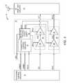
- FIG. 1shows an RF communications system 10 according to one embodiment of the RF communications system 10 .
- the RF communications system 10includes RF transmitter circuitry 12 , RF system control circuitry 14 , RF front-end circuitry 16 , an RF antenna 18 , and a DC power source 20 .
- the RF transmitter circuitry 12includes transmitter control circuitry 22 , an RF PA 24 , and an envelope tracking power supply 26 .
- the RF PA 24includes a driver stage 28 and a final stage 30 , which is coupled to the driver stage 28 .
- the RF front-end circuitry 16receives via the RF antenna 18 , processes, and forwards an RF receive signal RFR to the RF system control circuitry 14 .
- the transmitter control circuitry 22receives a first envelope power supply control signal VRMP 1 , a second envelope power supply control signal VRMP 2 , and a transmitter configuration signal PACS from the RF system control circuitry 14 .
- the RF system control circuitry 14selects either a first operating mode or a second operating mode, and the transmitter configuration signal PACS is indicative of the selection of the first operating mode or the second operating mode made by the RF system control circuitry 14 .
- the RF system control circuitry 14selects one of a group of operating modes, which includes the first operating mode and the second operating mode.
- the RF system control circuitry 14provides an RF input signal RFI to the RF PA 24 .
- the DC power source 20provides a DC source signal VDC to the envelope tracking power supply 26 .
- the DC power source 20is a battery.
- the envelope tracking power supply 26is coupled to the transmitter control circuitry 22 .
- the envelope tracking power supply 26provides a first envelope power supply signal EPS 1 to the driver stage 28 based on the first envelope power supply control signal VRMP 1 .
- the envelope tracking power supply 26provides a second envelope power supply signal EPS 2 to the final stage 30 based on the first envelope power supply control signal VRMP 1 .
- the envelope tracking power supply 26provides the second envelope power supply signal EPS 2 to the final stage 30 based on the second envelope power supply control signal VRMP 2 .
- the first envelope power supply signal EPS 1is based on the first envelope power supply control signal VRMP 1 during both the first operating mode and the second operating mode.
- the DC source signal VDCprovides power to the envelope tracking power supply 26 .
- both the first envelope power supply signal EPS 1 and the second envelope power supply signal EPS 2are further based on the DC source signal VDC.
- the first envelope power supply control signal VRMP 1is representative of a setpoint of the first envelope power supply signal EPS 1 .
- the first envelope power supply control signal VRMP 1is further representative of a setpoint of the second envelope power supply signal EPS 2 .
- the second envelope power supply control signal VRMP 2is representative of the setpoint of the second envelope power supply signal EPS 2 .
- the driver stage 28receives and amplifies the RF input signal RFI to provide a driver stage output signal DSO using the first envelope power supply signal EPS 1 , which provides power for amplification.
- the final stage 30receives and amplifies the driver stage output signal DSO to provide an RF transmit signal RFT using the second envelope power supply signal EPS 2 , which provides power for amplification.
- the RF PA 24receives and amplifies the RF input signal RFI to provide the RF transmit signal RFT using the driver stage 28 and the final stage 30 .
- the driver stage 28 and the final stage 30are coupled in series.
- the RF PA 24includes at least one additional driver stage (not shown) coupled in series with the driver stage 28 and the final stage 30 .
- the RF front-end circuitry 16receives, processes, and transmits the RF transmit signal RFT via the RF antenna 18 .
- the transmitter control circuitry 22configures the RF transmitter circuitry 12 based on the transmitter configuration signal PACS.
- the RF front-end circuitry 16includes at least one RF switch, at least one RF amplifier, at least one RF filter, at least one RF duplexer, at least one RF diplexer, at least one RF amplifier, the like, or any combination thereof.
- the RF system control circuitry 14is RF transceiver circuitry, which may include an RF transceiver IC, baseband controller circuitry, the like, or any combination thereof.
- the RF system control circuitry 14selects the second operating mode when a modulation bandwidth of the RF transmit signal RFT is greater than or equal to a bandwidth threshold. Otherwise, the RF system control circuitry 14 selects the first operating mode. In an alternate embodiment of the RF communications system 10 , the RF system control circuitry 14 selects the second operating mode when an output power from the RF PA 24 is greater than a power threshold. Otherwise, the RF system control circuitry 14 selects the first operating mode.
- the RF system control circuitry 14selects the second operating mode when the modulation bandwidth of the RF transmit signal RFT is greater than or equal to the bandwidth threshold and the output power from the RF PA 24 is greater than the power threshold. Otherwise, the RF system control circuitry 14 selects the first operating mode.
- the bandwidth thresholdis equal to about ten megahertz. In a second exemplary embodiment of the bandwidth threshold, the bandwidth threshold is equal to about eleven megahertz. In a third exemplary embodiment of the bandwidth threshold, the bandwidth threshold is equal to about twelve megahertz. In a fourth exemplary embodiment of the bandwidth threshold, the bandwidth threshold is equal to about thirteen megahertz. In a fifth exemplary embodiment of the bandwidth threshold, the bandwidth threshold is equal to about fourteen megahertz. In a sixth exemplary embodiment of the bandwidth threshold, the bandwidth threshold is equal to about fifteen megahertz. In a seventh exemplary embodiment of the bandwidth threshold, the bandwidth threshold is equal to about nine megahertz. In an eighth exemplary embodiment of the bandwidth threshold, the bandwidth threshold is equal to about eight megahertz.
- the bandwidth thresholdis equal to about seven megahertz. In a tenth exemplary embodiment of the bandwidth threshold, the bandwidth threshold is equal to about six megahertz. In an eleventh exemplary embodiment of the bandwidth threshold, the bandwidth threshold is equal to about five megahertz. In a twelfth exemplary embodiment of the bandwidth threshold, the bandwidth threshold is between about nine megahertz and about eleven megahertz. In a thirteenth exemplary embodiment of the bandwidth threshold, the bandwidth threshold is between about eight megahertz and about twelve megahertz. In a fourteenth exemplary embodiment of the bandwidth threshold, the bandwidth threshold is between about seven megahertz and about thirteen megahertz.
- the power thresholdis equal to about nine decibels below a maximum target output power from the RF PA 24 . In a second exemplary embodiment of the power threshold, the power threshold is equal to about eight decibels below the maximum target output power from the RF PA 24 . In a third exemplary embodiment of the power threshold, the power threshold is equal to about seven decibels below the maximum target output power from the RF PA 24 . In a fourth exemplary embodiment of the power threshold, the power threshold is equal to about six decibels below the maximum target output power from the RF PA 24 . In a fifth exemplary embodiment of the power threshold, the power threshold is equal to about ten decibels below the maximum target output power from the RF PA 24 .
- the power thresholdis equal to about eleven decibels below the maximum target output power from the RF PA 24 .
- the power thresholdis between about eight decibels below the maximum target output power from the RF PA 24 and about ten decibels below the maximum target output power from the RF PA 24 .
- the power thresholdis between about seven decibels below the maximum target output power from the RF PA 24 and about eleven decibels below the maximum target output power from the RF PA 24 .
- the maximum target output poweris equal to about 28 decibel milliwatts. In a second exemplary embodiment of the maximum target output power, the maximum target output power is equal to about 29 decibel milliwatts. In a third exemplary embodiment of the maximum target output power, the maximum target output power is equal to about 30 decibel milliwatts. In a fourth exemplary embodiment of the maximum target output power, the maximum target output power is equal to about 31 decibel milliwatts. In a fifth exemplary embodiment of the maximum target output power, the maximum target output power is equal to about 27 decibel milliwatts. In a sixth exemplary embodiment of the maximum target output power, the maximum target output power is equal to about 26 decibel milliwatts. In a seventh exemplary embodiment of the maximum target output power, the maximum target output power is equal to about 25 decibel milliwatts.
- the driver stage 28may operate most efficiently, particularly at high output power levels, when envelope power tracking is used.
- the first envelope power supply signal EPS 1is amplitude modulated, such that the first envelope power supply signal EPS 1 at least partially tracks an envelope of the driver stage output signal DSO.
- the driver stage 28may operate at adequate efficiency levels, particularly at low output power levels, when average power tracking is used.
- a magnitude of the first envelope power supply signal EPS 1is about constant, such that the magnitude of the first envelope power supply signal EPS 1 is large enough to allow the driver stage 28 to function properly.
- the first envelope power supply signal EPS 1at least partially tracks an average output power from the driver stage 28 .
- the final stage 30may operate most efficiently, particularly at high output power levels, when envelope power tracking is used.
- the second envelope power supply signal EPS 2is amplitude modulated, such that the second envelope power supply signal EPS 2 at least partially tracks an envelope of the RF transmit signal RFT.
- the final stage 30may operate at adequate efficiency levels, particularly at low output power levels, when average power tracking is used.
- a magnitude of the second envelope power supply signal EPS 2is about constant, such that the magnitude of the second envelope power supply signal EPS 2 is large enough to allow the final stage 30 to function properly.
- the second envelope power supply signal EPS 2at least partially tracks an average output power from the final stage 30 .
- the magnitude of the first envelope power supply signal EPS 1is about constant and the magnitude of the second envelope power supply signal EPS 2 is about constant, such that the magnitude of the first envelope power supply signal EPS 1 is about equal to the magnitude of the second envelope power supply signal EPS 2 .
- the magnitude of the first envelope power supply signal EPS 1is about constant and the magnitude of the second envelope power supply signal EPS 2 is about constant, such that the magnitude of the first envelope power supply signal EPS 1 is less than the magnitude of the second envelope power supply signal EPS 2 .
- the magnitude of the first envelope power supply signal EPS 1is about constant and the magnitude of the second envelope power supply signal EPS 2 is about constant, such that a voltage of the first envelope power supply signal EPS 1 is less than a voltage of the DC source signal VDC and a voltage of the second envelope power supply signal EPS 2 is less than the voltage of the DC source signal VDC.
- the magnitude of the first envelope power supply signal EPS 1is about constant and the magnitude of the second envelope power supply signal EPS 2 is about constant, such that the first envelope power supply signal EPS 1 at least partially tracks the average output power from the driver stage 28 and the second envelope power supply signal EPS 2 at least partially tracks the average output power from the final stage 30 .
- the first envelope power supply signal EPS 1is amplitude modulated and the second envelope power supply signal EPS 2 is amplitude modulated, such that an instantaneous magnitude of the first envelope power supply signal EPS 1 is about equal to an instantaneous magnitude of the second envelope power supply signal EPS 2 .
- the first envelope power supply signal EPS 1is amplitude modulated and the second envelope power supply signal EPS 2 is amplitude modulated, such that the instantaneous magnitude of the first envelope power supply signal EPS 1 is less than the instantaneous magnitude of the second envelope power supply signal EPS 2 .
- the first envelope power supply signal EPS 1is amplitude modulated and the second envelope power supply signal EPS 2 is amplitude modulated, such that the instantaneous magnitude of the first envelope power supply signal EPS 1 is less than the instantaneous magnitude of the second envelope power supply signal EPS 2 .
- the first envelope power supply signal EPS 1is amplitude modulated and the second envelope power supply signal EPS 2 is amplitude modulated, such that second envelope power supply signal EPS 2 at least partially tracks the envelope of the RF transmit signal RFT.
- the magnitude of the first envelope power supply signal EPS 1is about constant and the second envelope power supply signal EPS 2 is amplitude modulated, such that the second envelope power supply signal EPS 2 at least partially tracks the envelope of the RF transmit signal RFT.
- the magnitude of the first envelope power supply signal EPS 1is about constant and the second envelope power supply signal EPS 2 is amplitude modulated, such that the second envelope power supply signal EPS 2 at least partially tracks the envelope of the RF transmit signal RFT and the voltage of the first envelope power supply signal EPS 1 is less than the voltage of the DC source signal VDC.
- the magnitude of the first envelope power supply signal EPS 1is about constant and the second envelope power supply signal EPS 2 is amplitude modulated, such that the second envelope power supply signal EPS 2 at least partially tracks the envelope of the RF transmit signal RFT and the voltage of the first envelope power supply signal EPS 1 is greater than the voltage of the DC source signal VDC.
- the magnitude of the first envelope power supply signal EPS 1is about constant and the second envelope power supply signal EPS 2 is amplitude modulated, such that the second envelope power supply signal EPS 2 at least partially tracks the envelope of the RF transmit signal RFT and the voltage of the first envelope power supply signal EPS 1 is about equal to the voltage of the DC source signal VDC.
- the magnitude of the first envelope power supply signal EPS 1is about constant and the second envelope power supply signal EPS 2 is amplitude modulated, such that the second envelope power supply signal EPS 2 at least partially tracks the envelope of the RF transmit signal RFT and the first envelope power supply signal EPS 1 at least partially tracks the average output power from the driver stage 28 .
- the magnitude of the first envelope power supply signal EPS 1is about constant and the magnitude of the second envelope power supply signal EPS 2 is about constant.
- the magnitude of the first envelope power supply signal EPS 1is about constant and the magnitude of the second envelope power supply signal EPS 2 is about constant, such that the first envelope power supply signal EPS 1 at least partially tracks the average output power from the driver stage 28 and the second envelope power supply signal EPS 2 at least partially tracks the average output power from the final stage 30 .
- the magnitude of the first envelope power supply signal EPS 1is about constant and the magnitude of the second envelope power supply signal EPS 2 is about constant, such that the voltage of the first envelope power supply signal EPS 1 is less than the voltage of the DC source signal VDC and the voltage of the second envelope power supply signal EPS 2 is less than the voltage of the DC source signal VDC.
- the magnitude of the first envelope power supply signal EPS 1is about constant and the magnitude of the second envelope power supply signal EPS 2 is about constant, such that the voltage of the first envelope power supply signal EPS 1 is greater than the voltage of the DC source signal VDC and the voltage of the second envelope power supply signal EPS 2 is greater than the voltage of the DC source signal VDC.
- the magnitude of the first envelope power supply signal EPS 1is about constant and the magnitude of the second envelope power supply signal EPS 2 is about constant, such that the voltage of the first envelope power supply signal EPS 1 is less than the voltage of the DC source signal VDC and the voltage of the second envelope power supply signal EPS 2 is greater than the voltage of the DC source signal VDC.
- FIG. 2shows the RF communications system 10 according to an alternate embodiment of the RF communications system 10 .
- the RF communications system 10 illustrated in FIG. 2is similar to the RF communications system 10 illustrated in FIG. 1 , except in the RF communications system 10 illustrated in FIG. 2 , the RF transmitter circuitry 12 further includes a digital communications interface 32 , which is coupled between the transmitter control circuitry 22 and a digital communications bus 34 .
- the digital communications bus 34is also coupled to the RF system control circuitry 14 .
- the RF system control circuitry 14provides the first envelope power supply control signal VRMP 1 ( FIG. 1 ), the second envelope power supply control signal VRMP 2 ( FIG. 1 ), and the transmitter configuration signal PACS ( FIG. 1 ) to the transmitter control circuitry 22 via the digital communications bus 34 and the digital communications interface 32 .
- FIG. 3shows the RF communications system 10 according to an additional embodiment of the RF communications system 10 .
- the RF communications system 10 illustrated in FIG. 3is similar to the RF communications system 10 illustrated in FIG. 1 , except the RF transmitter circuitry 12 illustrated in FIG. 3 further includes an alternate RF PA 36 , which includes an alternate driver stage 38 and an alternate final stage 40 .
- the RF system control circuitry 14further selects either a primary operating mode or an alternate operating mode, and the transmitter configuration signal PACS is indicative of the selection of the primary operating mode or the alternate operating mode made by the RF system control circuitry 14 .
- the RF PA 24is enabled and the alternate RF PA 36 is disabled.
- the RF PA 24is disabled and the alternate RF PA 36 is enabled.
- the RF system control circuitry 14 , the RF front-end circuitry 16 , the transmitter control circuitry 22 , the RF PA 24 , and the envelope tracking power supply 26may function as previously described.
- the RF system control circuitry 14selects either the first operating mode or the second operating mode. During the alternate operating mode, the RF system control circuitry 14 provides an alternate RF input signal RFIA to the alternate RF PA 36 . During the alternate operating mode, the envelope tracking power supply 26 provides a third envelope power supply signal EPS 3 to the alternate driver stage 38 and a fourth envelope power supply signal EPS 4 to the alternate final stage 40 . During the alternate operating mode, and during both the first operating mode and the second operating mode, the alternate driver stage 38 receives and amplifies the alternate RF input signal RFIA to provide an alternate driver stage output signal DSA using the third envelope power supply signal EPS 3 , which provides power for amplification.
- EPS 3envelope power supply signal
- the alternate final stage 40receives and amplifies the alternate driver stage output signal DSA to provide an alternate RF transmit signal RFTA using the fourth envelope power supply signal EPS 4 , which provides power for amplification.
- the alternate RF PA 36receives and amplifies the alternate RF input signal RFIA to provide the alternate RF transmit signal RFTA using the alternate driver stage 38 and the alternate final stage 40 .
- the alternate driver stage 38 and the alternate final stage 40are coupled in series.
- the alternate RF PA 36includes at least one additional driver stage (not shown) coupled in series with the alternate driver stage 38 and the alternate final stage 40 .
- the RF front-end circuitry 16receives, processes, and transmits the alternate RF transmit signal RFTA via the RF antenna 18 .
- the third envelope power supply signal EPS 3behaves similarly to how the first envelope power supply signal EPS 1 behaves during the primary operating mode. Further, during the alternate operating mode, the fourth envelope power supply signal EPS 4 behaves similarly to how the second envelope power supply signal EPS 2 behaves during the primary operating mode.
- the third envelope power supply signal EPS 3behaves similarly to how the first envelope power supply signal EPS 1 behaves during the primary operating mode.
- the fourth envelope power supply signal EPS 4behaves similarly to how the first envelope power supply signal EPS 1 behaves during the primary operating mode.
- the third envelope power supply signal EPS 3behaves similarly to how the second envelope power supply signal EPS 2 behaves during the primary operating mode.
- the fourth envelope power supply signal EPS 4behaves similarly to how the second envelope power supply signal EPS 2 behaves during the primary operating mode.
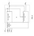
- FIG. 4shows details of the transmitter control circuitry 22 and the envelope tracking power supply 26 illustrated in FIG. 1 according to one embodiment of the transmitter control circuitry 22 and the envelope tracking power supply 26 .
- the envelope tracking power supply 26includes a final stage supply 42 and a driver stage supply 44 .
- the envelope tracking power supply 26is coupled to both the final stage supply 42 and the driver stage supply 44 .
- the DC power source 20provides the DC source signal VDC to the final stage supply 42 and to the driver stage supply 44 .
- the driver stage supply 44provides the first envelope power supply signal EPS 1 to the driver stage 28 ( FIG. 1 ) based on the first envelope power supply control signal VRMP 1 .
- the final stage supply 42provides the second envelope power supply signal EPS 2 to the final stage 30 ( FIG. 1 ) based on the first envelope power supply control signal VRMP 1 .
- the final stage supply 42provides the second envelope power supply signal EPS 2 to the final stage 30 ( FIG. 1 ) based on the second envelope power supply control signal VRMP 2 .
- the DC power source 20( FIG. 1 ) provides power to the driver stage supply 44 for the first envelope power supply signal EPS 1 via the DC source signal VDC.
- the DC power source 20( FIG. 1 ) provides power to the final stage supply 42 for the second envelope power supply signal EPS 2 via the DC source signal VDC.
- the driver stage supply 44includes a switching power supply.
- the final stage supply 42includes a switching power supply.
- FIG. 5shows details of the transmitter control circuitry 22 and the envelope tracking power supply 26 illustrated in FIG. 1 according to an alternate embodiment of the transmitter control circuitry 22 and the envelope tracking power supply 26 .
- FIG. 5shows details of the driver stage supply 44 illustrated in FIG. 4 , except the driver stage supply 44 illustrated in FIG. 5 does not receive the second envelope power supply signal EPS 2 .
- the driver stage supply 44includes a first linear voltage regulator 46 .
- the transmitter control circuitry 22provides a driver setpoint signal DSPS to a control input to the first linear voltage regulator 46 based on the first envelope power supply control signal VRMP 1 .
- the DC power source 20( FIG. 1 ) provides the DC source signal VDC to the first linear voltage regulator 46 .
- the first linear voltage regulator 46provides the first envelope power supply signal EPS 1 based on the driver setpoint signal DSPS and the DC source signal VDC.
- the DC power source 20( FIG. 1 ) provides power to the first linear voltage regulator 46 for the first envelope power supply signal EPS 1 via the DC source signal VDC.
- the first linear voltage regulator 46regulates a voltage magnitude of the first envelope power supply signal EPS 1 based on the driver setpoint signal DSPS as long as a voltage magnitude of the DC source signal VDC is high enough for the first linear voltage regulator 46 to maintain voltage regulation.
- the voltage magnitude of the first envelope power supply signal EPS 1is less than the voltage magnitude of the DC source signal VDC.
- the driver setpoint signal DSPSis further based on the transmitter configuration signal PACS, which may be based on configuration information as provided by the RF system control circuitry 14 ( FIG. 1 ).
- FIG. 6shows details of the transmitter control circuitry 22 and the envelope tracking power supply 26 illustrated in FIG. 1 according to an additional embodiment of the transmitter control circuitry 22 and the envelope tracking power supply 26 .
- FIG. 6shows details of the driver stage supply 44 illustrated in FIG. 4 .
- the driver stage supply 44includes the first linear voltage regulator 46 and a first multiplexer 48 .
- the transmitter control circuitry 22provides the driver setpoint signal DSPS to the control input to the first linear voltage regulator 46 based on the first envelope power supply control signal VRMP 1 .
- the DC power source 20( FIG. 1 ) provides the DC source signal VDC to the first linear voltage regulator 46 .
- the first linear voltage regulator 46feeds one input to the first multiplexer 48 .
- the transmitter control circuitry 22provides a first multiplexer control signal MCS 1 to a control input to the first multiplexer 48 based on the transmitter configuration signal PACS.
- the first multiplexer 48provides the first envelope power supply signal EPS 1 based on a selected one of the inputs to the first multiplexer 48 , as selected by the first multiplexer control signal MCS 1 .
- the first multiplexer 48When the first multiplexer control signal MCS 1 selects the second envelope power supply signal EPS 2 , the first multiplexer 48 receives and forwards the second envelope power supply signal EPS 2 to provide the first envelope power supply signal EPS 1 . Conversely, when the first multiplexer control signal MCS 1 selects the output from the first linear voltage regulator 46 , the first multiplexer 48 receives and forwards the signal provided from the output from the first linear voltage regulator 46 to provide the first envelope power supply signal EPS 1 .
- the first envelope power supply signal EPS 1is based on the second envelope power supply signal EPS 2 , and during the second operating mode, the first envelope power supply signal EPS 1 is based on the driver setpoint signal DSPS.
- the first envelope power supply signal EPS 1is based on the driver setpoint signal DSPS, and during the second operating mode, the first envelope power supply signal EPS 1 is based on the driver setpoint signal DSPS.
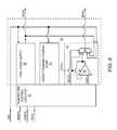
- FIG. 7shows details of the transmitter control circuitry 22 and the envelope tracking power supply 26 illustrated in FIG. 1 according to another embodiment of the transmitter control circuitry 22 and the envelope tracking power supply 26 .
- the envelope tracking power supply 26includes the final stage supply 42 , the driver stage supply 44 , and a capacitor-based charge pump 50 .
- the envelope tracking power supply 26is coupled to the final stage supply 42 , to the driver stage supply 44 , and to the capacitor-based charge pump 50 .
- the DC power source 20provides the DC source signal VDC to the final stage supply 42 , to the driver stage supply 44 , and to the capacitor-based charge pump 50 .
- the driver stage supply 44provides the first envelope power supply signal EPS 1 to the driver stage 28 ( FIG. 1 ) based on the first envelope power supply control signal VRMP 1 .
- the final stage supply 42provides the second envelope power supply signal EPS 2 to the final stage 30 ( FIG. 1 ) based on the first envelope power supply control signal VRMP 1 .
- the final stage supply 42provides the second envelope power supply signal EPS 2 to the final stage 30 ( FIG. 1 ) based on the second envelope power supply control signal VRMP 2 .
- the DC power source 20( FIG. 1 ) provides power to the final stage supply 42 for the second envelope power supply signal EPS 2 via the DC source signal VDC.
- the capacitor-based charge pump 50provides power to the driver stage supply 44 for the first envelope power supply signal EPS 1 via a first charge pump output signal CPO 1 .
- the DC power source 20( FIG. 1 ) provides power to the capacitor-based charge pump 50 for the first charge pump output signal CPO 1 via the DC source signal VDC.
- a voltage magnitude of the first charge pump output signal CPO 1may be greater than, less than, or equal to the voltage magnitude of the DC source signal VDC.
- the driver stage supply 44does not receive the DC source signal VDC.
- FIG. 8shows details of the transmitter control circuitry 22 and the envelope tracking power supply 26 illustrated in FIG. 1 according to a further embodiment of the transmitter control circuitry 22 and the envelope tracking power supply 26 .
- the transmitter control circuitry 22 and the envelope tracking power supply 26 illustrated in FIG. 8are similar to the transmitter control circuitry 22 and the envelope tracking power supply 26 illustrated in FIG. 7 , except details of the driver stage supply 44 illustrated in FIG. 7 are shown in FIG. 8 .
- the driver stage supply 44 shown in FIG. 8is similar to the driver stage supply 44 illustrated in FIG. 6 , except in the driver stage supply 44 illustrated in FIG. 8 , the capacitor-based charge pump 50 provides power to the first linear voltage regulator 46 via the first charge pump output signal CPO 1 instead of the DC power source 20 ( FIG. 1 ) providing power to the first linear voltage regulator 46 via the DC source signal VDC. Further, the first multiplexer 48 illustrated in FIG. 6 has two inputs, whereas the first multiplexer 48 illustrated in FIG. 8 has four inputs.
- the driver stage supply 44includes the first linear voltage regulator 46 and the first multiplexer 48 .
- the transmitter control circuitry 22provides the driver setpoint signal DSPS to the control input to the first linear voltage regulator 46 based on the first envelope power supply control signal VRMP 1 .
- the capacitor-based charge pump 50provides power to the first linear voltage regulator 46 via the first charge pump output signal CPO 1 . Further, the capacitor-based charge pump 50 feeds the first charge pump output signal CPO 1 to a first input to the first multiplexer 48 .
- the first linear voltage regulator 46feeds a second input to the first multiplexer 48 .
- the DC power source 20( FIG. 1 ) feeds the DC source signal VDC to a third input to the first multiplexer 48 .
- the final stage supply 42feeds the second envelope power supply signal EPS 2 to a fourth input to the first multiplexer 48 .
- the transmitter control circuitry 22provides the first multiplexer control signal MCS 1 to the control input to the first multiplexer 48 based on the transmitter configuration signal PACS.
- the first multiplexer 48provides the first envelope power supply signal EPS 1 based on a selected one of the four inputs to the first multiplexer 48 , as selected by the first multiplexer control signal MCS 1 .
- the first multiplexer 48When the first multiplexer control signal MCS 1 selects the first input to the first multiplexer 48 , the first multiplexer 48 receives and forwards the first charge pump output signal CPO 1 to provide the first envelope power supply signal EPS 1 .
- the first multiplexer control signal MCS 1selects the second input to the first multiplexer 48 , the first multiplexer 48 receives and forwards the signal provided from the output from the first linear voltage regulator 46 to provide the first envelope power supply signal EPS 1 .
- the first multiplexer control signal MCS 1selects the third input to the first multiplexer 48 , the first multiplexer 48 receives and forwards the DC source signal VDC to provide the first envelope power supply signal EPS 1 .
- the first multiplexer control signal MCS 1selects the fourth input to the first multiplexer 48 , the first multiplexer 48 receives and forwards the second envelope power supply signal EPS 2 to provide the first envelope power supply signal EPS 1 .
- the first envelope power supply signal EPS 1is based on the second envelope power supply signal EPS 2 , and during the second operating mode, the first envelope power supply signal EPS 1 is based on the driver setpoint signal DSPS.
- the first envelope power supply signal EPS 1is based on the second envelope power supply signal EPS 2
- the first envelope power supply signal EPS 1is based on the DC source signal VDC.
- the first envelope power supply signal EPS 1is based on the second envelope power supply signal EPS 2 , and during the second operating mode, the first envelope power supply signal EPS 1 is based on the first charge pump output signal CPO 1 .
- the first envelope power supply signal EPS 1is based on the driver setpoint signal DSPS, and during the second operating mode, the first envelope power supply signal EPS 1 is based on the driver setpoint signal DSPS.
- the first multiplexer 48does not receive the DC source signal VDC. In another embodiment of the driver stage supply 44 , the first multiplexer 48 does not receive the first charge pump output signal CPO 1 . In a further embodiment of the driver stage supply 44 , the first multiplexer 48 does not receive the second envelope power supply signal EPS 2 . In an additional embodiment of the driver stage supply 44 , the first linear voltage regulator 46 is omitted. In a supplemental embodiment of the driver stage supply 44 , the first multiplexer 48 may not receive any or all of the DC source signal VDC, the first charge pump output signal CPO 1 , and the second envelope power supply signal EPS 2 ; and the first linear voltage regulator 46 may be omitted.
- FIG. 9shows details of the transmitter control circuitry 22 and the envelope tracking power supply 26 illustrated in FIG. 1 according to a supplemental embodiment of the transmitter control circuitry 22 and the envelope tracking power supply 26 .
- FIG. 9shows details of the final stage supply 42 illustrated in FIG. 7 .
- the final stage supply 42includes a primary switching supply 52 and a parallel amplifier 54 , both of which are coupled to the transmitter control circuitry 22 .
- the transmitter control circuitry 22controls the parallel amplifier 54 and the primary switching supply 52 .
- the parallel amplifier 54 and the primary switching supply 52provide the second envelope power supply signal EPS 2 , such that the parallel amplifier 54 partially provides the second envelope power supply signal EPS 2 and the primary switching supply 52 partially provides the second envelope power supply signal EPS 2 .
- the DC power source 20( FIG. 1 ) provides power to the primary switching supply 52 for the second envelope power supply signal EPS 2 via the DC source signal VDC.
- the DC power source 20FIG. 1
- the primary switching supply 52may provide power more efficiently than the parallel amplifier 54 .
- the parallel amplifier 54may provide the second envelope power supply signal EPS 2 more accurately than the primary switching supply 52 .
- the parallel amplifier 54regulates a voltage of the second envelope power supply signal EPS 2 based on the setpoint of the second envelope power supply signal EPS 2 , and the primary switching supply 52 operates to drive an output current from the parallel amplifier 54 toward zero to maximize efficiency.
- the parallel amplifier 54behaves like a voltage source and the primary switching supply 52 behaves like a current source.
- the parallel amplifier 54provides a current sense signal CSS to the primary switching supply 52 .
- the current sense signal CSSis indicative of the output current from the parallel amplifier 54 .
- the primary switching supply 52regulates a duty-cycle of the primary switching supply 52 to drive the output current from the parallel amplifier 54 toward zero, as indicated by the current sense signal CSS.
- a magnitude of the current sense signal CSSis equal to about zero when the output current from the parallel amplifier 54 is equal to about zero.
- FIG. 10shows details of the transmitter control circuitry 22 and the envelope tracking power supply 26 illustrated in FIG. 1 according to one embodiment of the transmitter control circuitry 22 and the envelope tracking power supply 26 .
- FIG. 10shows details of the parallel amplifier 54 illustrated in FIG. 9 .
- the parallel amplifier 54includes a second linear voltage regulator 56 and a first capacitive element C 1 .
- the transmitter control circuitry 22provides a final setpoint signal FSPS to a control input to the second linear voltage regulator 56 .
- the first capacitive element C 1is coupled in series between an output from the second linear voltage regulator 56 and an output from the primary switching supply 52 to provide the second envelope power supply signal EPS 2 .
- the second linear voltage regulator 56provides the current sense signal CSS to the primary switching supply 52 based on a current from the output from the second linear voltage regulator 56 .
- the final setpoint signal FSPSis based on the first envelope power supply control signal VRMP 1 and during the second operating mode, the final setpoint signal FSPS is based on the second envelope power supply control signal VRMP 2 .
- the DC power source 20( FIG. 1 ) provides the DC source signal VDC to the second linear voltage regulator 56 .
- the second linear voltage regulator 56at least partially provides the second envelope power supply signal EPS 2 based on the final setpoint signal FSPS and the DC source signal VDC.
- the DC power source 20( FIG. 1 ) provides at least partial power to the second linear voltage regulator 56 for the second envelope power supply signal EPS 2 via the DC source signal VDC.
- the output from the second linear voltage regulator 56cannot be driven higher than the voltage magnitude of the DC source signal VDC.
- the output of the primary switching supply 52is capable of being driven to a voltage magnitude higher than the voltage magnitude of the DC source signal VDC.
- an offset voltagecan be applied across the first capacitive element C 1 , which allows the second linear voltage regulator 56 to function within its operating range, while a voltage magnitude of the second envelope power supply signal EPS 2 is higher than the voltage magnitude of the DC source signal VDC.
- the final setpoint signal FSPSis further based on the transmitter configuration signal PACS, which may be based on configuration information as provided by the RF system control circuitry 14 ( FIG. 1 ).
- FIG. 11shows details of the transmitter control circuitry 22 and the envelope tracking power supply 26 illustrated in FIG. 1 according to an alternate embodiment of the transmitter control circuitry 22 and the envelope tracking power supply 26 .
- the parallel amplifier 54 illustrated in FIG. 11is similar to the parallel amplifier 54 illustrated in FIG. 10 , except the parallel amplifier 54 illustrated in FIG. 11 further includes a third linear voltage regulator 58 .
- the third linear voltage regulator 58may be used instead of the second linear voltage regulator 56 and the primary switching supply 52 .
- the RF system control circuitry 14FIG.
- the transmitter configuration signal PACSis indicative of the selection of the first final stage operating mode or the second final stage operating mode made by the RF system control circuitry 14 ( FIG. 1 ).
- the primary switching supply 52 and the second linear voltage regulator 56are enabled and the third linear voltage regulator 58 is disabled.
- the third linear voltage regulator 58is enabled, and either both the primary switching supply 52 and the second linear voltage regulator 56 are disabled, or the primary switching supply 52 is enabled and the second linear voltage regulator 56 is disabled.
- the transmitter control circuitry 22provides the final setpoint signal FSPS to a control input to the third linear voltage regulator 58 .
- the output from the second linear voltage regulator 56is coupled to the output from the primary switching supply 52 to at least partially provide the second envelope power supply signal EPS 2 during the second final stage operating mode.
- the DC power source 20( FIG. 1 ) provides the DC source signal VDC to the third linear voltage regulator 58 .
- the third linear voltage regulator 58at least partially provides the second envelope power supply signal EPS 2 based on the final setpoint signal FSPS and the DC source signal VDC.
- the DC power source 20( FIG. 1 ) provides at least partial power to the third linear voltage regulator 58 for the second envelope power supply signal EPS 2 via the DC source signal VDC.
- the third linear voltage regulator 58regulates a voltage magnitude of the second envelope power supply signal EPS 2 based on the final setpoint signal FSPS as long as a voltage magnitude of the DC source signal VDC is high enough for the third linear voltage regulator 58 to maintain voltage regulation.
- the voltage magnitude of the second envelope power supply signal EPS 2is less than the voltage magnitude of the DC source signal VDC.
- FIG. 12shows details of the transmitter control circuitry 22 and the envelope tracking power supply 26 illustrated in FIG. 1 according to an additional embodiment of the transmitter control circuitry 22 and the envelope tracking power supply 26 .
- the envelope tracking power supply 26 illustrated in FIG. 12is similar to the envelope tracking power supply 26 illustrated in FIG. 9 , except in the envelope tracking power supply 26 illustrated in FIG. 12 , the capacitor-based charge pump 50 provides power to the parallel amplifier 54 for the second envelope power supply signal EPS 2 via a second charge pump output signal CPO 2 instead of the DC power source 20 ( FIG. 1 ) providing power to the parallel amplifier 54 via the DC source signal VDC.
- the second charge pump output signal CPO 2may provide more flexibility, since a voltage magnitude of the second charge pump output signal CPO 2 may be greater than, less than, or equal to the voltage magnitude of the DC source signal VDC.
- the capacitor-based charge pump 50provides the first charge pump output signal CPO 1 based on the DC source signal VDC, such that the first envelope power supply signal EPS 1 is further based on the first charge pump output signal CPO 1
- the capacitor-based charge pump 50provides the second charge pump output signal CPO 2 based on the DC source signal VDC, such that the second envelope power supply signal EPS 2 is further based on the second charge pump output signal CPO 2
- the envelope tracking power supply 26further includes a first flying capacitive element C 1 F and a second flying capacitive element C 2 F, both of which are coupled to the capacitor-based charge pump 50 .
- the first flying capacitive element C 1 F and the second flying capacitive element C 2 Fprovide a pair of flying capacitive elements, which are coupled to the capacitor-based charge pump 50 .
- the capacitor-based charge pump 50transfers charge from the DC power source 20 ( FIG. 1 ) to the driver stage 28 ( FIG. 1 ) and to the final stage 30 using the pair of flying capacitive elements.
- the driver stage supply 44provides the first envelope power supply signal EPS 1 to the driver stage 28 ( FIG. 1 ) further based on the first charge pump output signal CPO 1 .
- the parallel amplifier 54at least partially provides the second envelope power supply signal EPS 2 to the final stage 30 ( FIG. 1 ) further based on the second charge pump output signal CPO 2 .
- a ratio of a voltage magnitude of the second charge pump output signal CPO 2 divided by a voltage magnitude of the DC source signal VDCis equal to about five-fourths, and a ratio of a voltage magnitude of the first charge pump output signal CPO 1 divided by the voltage magnitude of the DC source signal VDC is equal to about one.
- the ratio of the voltage magnitude of the second charge pump output signal CPO 2 divided by the voltage magnitude of the DC source signal VDCis equal to about five-fourths, and a ratio of the voltage magnitude of the first charge pump output signal CPO 1 divided by the voltage magnitude of the DC source signal VDC is equal to about three-fourths.
- the ratio of the voltage magnitude of the second charge pump output signal CPO 2 divided by the voltage magnitude of the DC source signal VDCis equal to about five-fourths, and a ratio of the voltage magnitude of the first charge pump output signal CPO 1 divided by the voltage magnitude of the DC source signal VDC is equal to about one-fourth.
- a ratio of the voltage magnitude of the second charge pump output signal CPO 2 divided by the voltage magnitude of the DC source signal VDCis equal to about one, and a ratio of the voltage magnitude of the first charge pump output signal CPO 1 divided by the voltage magnitude of the DC source signal VDC is equal to about one.
- the ratio of the voltage magnitude of the second charge pump output signal CPO 2 divided by the voltage magnitude of the DC source signal VDCis equal to about one, and a ratio of the voltage magnitude of the first charge pump output signal CPO 1 divided by the voltage magnitude of the DC source signal VDC is equal to about three-fourths.
- the ratio of the voltage magnitude of the second charge pump output signal CPO 2 divided by the voltage magnitude of the DC source signal VDCis equal to about one, and a ratio of the voltage magnitude of the first charge pump output signal CPO 1 divided by the voltage magnitude of the DC source signal VDC is equal to about two-thirds.
- the ratio of the voltage magnitude of the second charge pump output signal CPO 2 divided by the voltage magnitude of the DC source signal VDCis equal to about one, and a ratio of the voltage magnitude of the first charge pump output signal CPO 1 divided by the voltage magnitude of the DC source signal VDC is equal to about one-half.
- the ratio of the voltage magnitude of the second charge pump output signal CPO 2 divided by the voltage magnitude of the DC source signal VDCis equal to about one, and a ratio of the voltage magnitude of the first charge pump output signal CPO 1 divided by the voltage magnitude of the DC source signal VDC is equal to about one-third.
- the ratio of the voltage magnitude of the second charge pump output signal CPO 2 divided by the voltage magnitude of the DC source signal VDCis equal to about one, and a ratio of the voltage magnitude of the first charge pump output signal CPO 1 divided by the voltage magnitude of the DC source signal VDC is equal to about one-fourth.
- a ratio of the voltage magnitude of the second charge pump output signal CPO 2 divided by the voltage magnitude of the DC source signal VDCis equal to about four-thirds, and a ratio of the voltage magnitude of the first charge pump output signal CPO 1 divided by the voltage magnitude of the DC source signal VDC is equal to about one.
- the ratio of the voltage magnitude of the second charge pump output signal CPO 2 divided by the voltage magnitude of the DC source signal VDCis equal to about four-thirds, and a ratio of the voltage magnitude of the first charge pump output signal CPO 1 divided by the voltage magnitude of the DC source signal VDC is equal to about two-thirds.
- the ratio of the voltage magnitude of the second charge pump output signal CPO 2 divided by the voltage magnitude of the DC source signal VDCis equal to about four-thirds, and a ratio of the voltage magnitude of the first charge pump output signal CPO 1 divided by the voltage magnitude of the DC source signal VDC is equal to about one-third.
- a ratio of the voltage magnitude of the second charge pump output signal CPO 2 divided by the voltage magnitude of the DC source signal VDCis equal to about three-halves, and a ratio of the voltage magnitude of the first charge pump output signal CPO 1 divided by the voltage magnitude of the DC source signal VDC is equal to about one.
- the ratio of the voltage magnitude of the second charge pump output signal CPO 2 divided by the voltage magnitude of the DC source signal VDCis equal to about three-halves, and a ratio of the voltage magnitude of the first charge pump output signal CPO 1 divided by the voltage magnitude of the DC source signal VDC is equal to about one-half.
- FIG. 13shows details of the transmitter control circuitry 22 and the envelope tracking power supply 26 illustrated in FIG. 1 according to another embodiment of the transmitter control circuitry 22 and the envelope tracking power supply 26 .
- the parallel amplifier 54 illustrated in FIG. 13is similar to the parallel amplifier 54 illustrated in FIG. 10 , except in the parallel amplifier 54 illustrated in FIG. 13 , the second linear voltage regulator 56 is powered using the second charge pump output signal CPO 2 instead of the DC source signal VDC.
- the second charge pump output signal CPO 2provides greater flexibility since the voltage magnitude of the second charge pump output signal CPO 2 may be greater than, less than, or equal to the voltage magnitude of the DC source signal VDC.
- FIG. 14shows details of the transmitter control circuitry 22 and the envelope tracking power supply 26 illustrated in FIG. 1 according to a further embodiment of the transmitter control circuitry 22 and the envelope tracking power supply 26 .
- the parallel amplifier 54 illustrated in FIG. 14is similar to the parallel amplifier 54 illustrated in FIG. 11 , except in the parallel amplifier 54 illustrated in FIG. 14 , the second linear voltage regulator 56 and the third linear voltage regulator 58 are powered using the second charge pump output signal CPO 2 instead of the DC source signal VDC.
- the second charge pump output signal CPO 2provides greater flexibility since the voltage magnitude of the second charge pump output signal CPO 2 may be greater than, less than, or equal to the voltage magnitude of the DC source signal VDC.
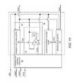
- FIG. 15shows details of the transmitter control circuitry 22 and the envelope tracking power supply 26 illustrated in FIG. 1 according to a supplemental embodiment of the transmitter control circuitry 22 and the envelope tracking power supply 26 .
- the envelope tracking power supply 26 illustrated in FIG. 15is similar to the envelope tracking power supply 26 illustrated in FIG. 12 , except the envelope tracking power supply 26 illustrated in FIG. 15 further includes a second multiplexer 60 .
- the capacitor-based charge pump 50provides the first charge pump output signal CPO 1 to one input to the second multiplexer 60 instead of providing the first charge pump output signal CPO 1 to the driver stage supply 44 .
- the DC power source 20( FIG. 1 ) provides the DC source signal VDC to another input to the second multiplexer 60 .
- the second multiplexer 60provides a driver stage source signal DSSS to the driver stage supply 44 based on a selected one of the first charge pump output signal CPO 1 and the DC source signal VDC. As such, the second multiplexer 60 provides power to the driver stage supply 44 via the driver stage source signal DSSS.
- the transmitter control circuitry 22provides a second multiplexer control signal MCS 2 to a control input to the second multiplexer 60 based on the transmitter configuration signal PACS, which may be based on configuration information as provided by the RF system control circuitry 14 ( FIG. 1 ).
- the second multiplexer 60provides the driver stage source signal DSSS based on a selected one of the inputs to the second multiplexer 60 , as selected by the first multiplexer control signal MCS 1 .
- the second multiplexer control signal MCS 2selects the first charge pump output signal CPO 1
- the second multiplexer 60receives and forwards the first charge pump output signal CPO 1 to provide the driver stage source signal DSSS.
- the second multiplexer control signal MCS 2selects the DC source signal VDC
- the second multiplexer 60receives and forwards the DC source signal VDC to provide the driver stage source signal DSSS.
- the second multiplexer 60receives and forwards the selected one of the first charge pump output signal CPO 1 and the DC source signal VDC. Further, the driver stage 28 ( FIG. 1 ) provides the first envelope power supply signal EPS 1 ( FIG. 1 ) further based on the selected one of the first charge pump output signal CPO 1 and the DC source signal VDC.
- the voltage magnitude of the first charge pump output signal CPO 1is less than the voltage magnitude of the DC source signal VDC.
- the transmitter control circuitry 22may select the first charge pump output signal CPO 1 to be forwarded when the voltage magnitude of the DC source signal VDC is too high, which may improve efficiency.
Landscapes
- Engineering & Computer Science (AREA)
- Power Engineering (AREA)
- Microelectronics & Electronic Packaging (AREA)
- Amplifiers (AREA)
- Transmitters (AREA)
Abstract
Description
Claims (28)
Priority Applications (1)
| Application Number | Priority Date | Filing Date | Title |
|---|---|---|---|
| US13/602,856US8942652B2 (en) | 2011-09-02 | 2012-09-04 | Split VCC and common VCC power management architecture for envelope tracking |
Applications Claiming Priority (2)
| Application Number | Priority Date | Filing Date | Title |
|---|---|---|---|
| US201161530625P | 2011-09-02 | 2011-09-02 | |
| US13/602,856US8942652B2 (en) | 2011-09-02 | 2012-09-04 | Split VCC and common VCC power management architecture for envelope tracking |
Publications (2)
| Publication Number | Publication Date |
|---|---|
| US20130234793A1 US20130234793A1 (en) | 2013-09-12 |
| US8942652B2true US8942652B2 (en) | 2015-01-27 |
Family
ID=47023061
Family Applications (1)
| Application Number | Title | Priority Date | Filing Date |
|---|---|---|---|
| US13/602,856ActiveUS8942652B2 (en) | 2011-09-02 | 2012-09-04 | Split VCC and common VCC power management architecture for envelope tracking |
Country Status (3)
| Country | Link |
|---|---|
| US (1) | US8942652B2 (en) |
| CN (1) | CN103858338B (en) |
| WO (1) | WO2013033700A1 (en) |
Cited By (36)
| Publication number | Priority date | Publication date | Assignee | Title |
|---|---|---|---|---|
| US20140155116A1 (en)* | 2012-12-03 | 2014-06-05 | Broadcom Corporation | Dynamic Operating Bandwidth Configuration for an Envelope Tracker |
| US9207692B2 (en) | 2012-10-18 | 2015-12-08 | Rf Micro Devices, Inc. | Transitioning from envelope tracking to average power tracking |
| US9225231B2 (en) | 2012-09-14 | 2015-12-29 | Rf Micro Devices, Inc. | Open loop ripple cancellation circuit in a DC-DC converter |
| US9247496B2 (en) | 2011-05-05 | 2016-01-26 | Rf Micro Devices, Inc. | Power loop control based envelope tracking |
| US9246460B2 (en) | 2011-05-05 | 2016-01-26 | Rf Micro Devices, Inc. | Power management architecture for modulated and constant supply operation |
| US9250643B2 (en) | 2011-11-30 | 2016-02-02 | Rf Micro Devices, Inc. | Using a switching signal delay to reduce noise from a switching power supply |
| US9256234B2 (en) | 2011-12-01 | 2016-02-09 | Rf Micro Devices, Inc. | Voltage offset loop for a switching controller |
| US9263996B2 (en) | 2011-07-20 | 2016-02-16 | Rf Micro Devices, Inc. | Quasi iso-gain supply voltage function for envelope tracking systems |
| US9280163B2 (en) | 2011-12-01 | 2016-03-08 | Rf Micro Devices, Inc. | Average power tracking controller |
| US9294041B2 (en) | 2011-10-26 | 2016-03-22 | Rf Micro Devices, Inc. | Average frequency control of switcher for envelope tracking |
| US9300252B2 (en) | 2013-01-24 | 2016-03-29 | Rf Micro Devices, Inc. | Communications based adjustments of a parallel amplifier power supply |
| US9298198B2 (en) | 2011-12-28 | 2016-03-29 | Rf Micro Devices, Inc. | Noise reduction for envelope tracking |
| US20160164553A1 (en)* | 2013-06-27 | 2016-06-09 | Hiroshi Kurihara | Linear Composite Transmitter Utilizing Composite Power Amplification |
| US9374005B2 (en) | 2013-08-13 | 2016-06-21 | Rf Micro Devices, Inc. | Expanded range DC-DC converter |
| US9377797B2 (en) | 2011-12-01 | 2016-06-28 | Rf Micro Devices, Inc. | Multiple mode RF power converter |
| US9379667B2 (en) | 2011-05-05 | 2016-06-28 | Rf Micro Devices, Inc. | Multiple power supply input parallel amplifier based envelope tracking |
| US9401678B2 (en) | 2010-04-19 | 2016-07-26 | Rf Micro Devices, Inc. | Output impedance compensation of a pseudo-envelope follower power management system |
| US9431974B2 (en) | 2010-04-19 | 2016-08-30 | Qorvo Us, Inc. | Pseudo-envelope following feedback delay compensation |
| US9479118B2 (en) | 2013-04-16 | 2016-10-25 | Rf Micro Devices, Inc. | Dual instantaneous envelope tracking |
| US9484797B2 (en) | 2011-10-26 | 2016-11-01 | Qorvo Us, Inc. | RF switching converter with ripple correction |
| US9494962B2 (en) | 2011-12-02 | 2016-11-15 | Rf Micro Devices, Inc. | Phase reconfigurable switching power supply |
| US9515621B2 (en) | 2011-11-30 | 2016-12-06 | Qorvo Us, Inc. | Multimode RF amplifier system |
| US9614476B2 (en) | 2014-07-01 | 2017-04-04 | Qorvo Us, Inc. | Group delay calibration of RF envelope tracking |
| US9621113B2 (en) | 2010-04-19 | 2017-04-11 | Qorvo Us, Inc. | Pseudo-envelope following power management system |
| US9627975B2 (en) | 2012-11-16 | 2017-04-18 | Qorvo Us, Inc. | Modulated power supply system and method with automatic transition between buck and boost modes |
| US9813036B2 (en) | 2011-12-16 | 2017-11-07 | Qorvo Us, Inc. | Dynamic loadline power amplifier with baseband linearization |
| US9843294B2 (en) | 2015-07-01 | 2017-12-12 | Qorvo Us, Inc. | Dual-mode envelope tracking power converter circuitry |
| US9912297B2 (en) | 2015-07-01 | 2018-03-06 | Qorvo Us, Inc. | Envelope tracking power converter circuitry |
| US9954436B2 (en) | 2010-09-29 | 2018-04-24 | Qorvo Us, Inc. | Single μC-buckboost converter with multiple regulated supply outputs |
| US9973147B2 (en) | 2016-05-10 | 2018-05-15 | Qorvo Us, Inc. | Envelope tracking power management circuit |
| US10056864B2 (en) | 2017-01-12 | 2018-08-21 | Qualcomm Incorporated | Efficient wideband envelope tracking power amplifier |
| US20190253023A1 (en)* | 2018-02-09 | 2019-08-15 | Research & Business Foundation Sungkyunkwan University | Dual-output and dual-mode supply modulator, two-stage power amplifier using the same, and supply modulation method therefor |
| US10476437B2 (en) | 2018-03-15 | 2019-11-12 | Qorvo Us, Inc. | Multimode voltage tracker circuit |
| US11133833B2 (en) | 2013-02-11 | 2021-09-28 | Qualcomm Incorporated | Power tracker for multiple transmit signals sent simultaneously |
| US11949384B2 (en) | 2020-06-29 | 2024-04-02 | Samsung Electronics Co., Ltd. | Supply modulator and wireless communication apparatus including the same |
| TWI843259B (en)* | 2022-02-18 | 2024-05-21 | 聯發科技股份有限公司 | Radio frequency module and associated method with envelope tracking power supply |
Families Citing this family (5)
| Publication number | Priority date | Publication date | Assignee | Title |
|---|---|---|---|---|
| US8648657B1 (en)* | 2012-08-13 | 2014-02-11 | Broadcom Corporation | Mobile device including a power amplifier with selectable voltage supply |
| US9991856B2 (en)* | 2014-09-25 | 2018-06-05 | Skyworks Solutions, Inc. | Variable load power amplifier supporting dual-mode envelope tracking and average power tracking performance |
| GB201613948D0 (en)* | 2016-08-15 | 2016-09-28 | Univ Surrey | Load modulation in signal transmission |
| US10320430B2 (en)* | 2017-09-29 | 2019-06-11 | Intel Corporation | Transmitter with power supply rejection |
| JP2020182090A (en)* | 2019-04-24 | 2020-11-05 | 株式会社村田製作所 | Power amplifier circuit |
Citations (256)
| Publication number | Priority date | Publication date | Assignee | Title |
|---|---|---|---|---|
| US3969682A (en) | 1974-10-21 | 1976-07-13 | Oberheim Electronics Inc. | Circuit for dynamic control of phase shift |
| US3980964A (en) | 1974-05-20 | 1976-09-14 | Grodinsky Robert M | Noise reduction circuit |
| US4587552A (en) | 1983-09-02 | 1986-05-06 | Rca Corporation | Apparatus for generating the magnitude of the vector sum of two orthogonal signals as for use in a digital TV receiver |
| US4692889A (en) | 1984-09-28 | 1987-09-08 | Rca Corporation | Circuitry for calculating magnitude of vector sum from its orthogonal components in digital television receiver |
| US4831258A (en) | 1988-03-04 | 1989-05-16 | Exergen Corporation | Dual sensor radiation detector |
| US4996500A (en) | 1989-10-24 | 1991-02-26 | Hewlett-Packard Company | Automatic control system |
| US5099203A (en) | 1990-06-05 | 1992-03-24 | Continental Electronics Corporation | Power amplifier having multiple switched stages and method of operating same |
| US5146504A (en) | 1990-12-07 | 1992-09-08 | Motorola, Inc. | Speech selective automatic gain control |
| US5187396A (en) | 1991-05-22 | 1993-02-16 | Benchmarq Microelectronics, Inc. | Differential comparator powered from signal input terminals for use in power switching applications |
| US5311309A (en) | 1990-06-01 | 1994-05-10 | Thomson Consumer Electronics, Inc. | Luminance processing system for compressing and expanding video data |
| US5317217A (en) | 1990-11-29 | 1994-05-31 | Deutsche Thomson-Brandt Gmbh | Universal active filter |
| US5351087A (en) | 1990-06-01 | 1994-09-27 | Thomson Consumer Electronics, Inc. | Two stage interpolation system |
| US5414614A (en) | 1994-06-06 | 1995-05-09 | Motorola, Inc. | Dynamically configurable switched capacitor power supply and method |
| US5420643A (en) | 1990-06-01 | 1995-05-30 | Thomson Consumer Electronics, Inc. | Chrominance processing system for compressing and expanding video data |
| US5486871A (en) | 1990-06-01 | 1996-01-23 | Thomson Consumer Electronics, Inc. | Automatic letterbox detection |
| US5532916A (en) | 1992-09-02 | 1996-07-02 | Nec Corporation | Voltage converting circuit and multiphase clock generating circuit used for driving the same |
| US5541547A (en) | 1995-05-03 | 1996-07-30 | Sun Microsystems, Inc. | Test generator system for controllably inducing power pin latch-up and signal pin latch-up in a CMOS device |
| US5581454A (en) | 1994-11-22 | 1996-12-03 | Collins; Hansel | High power switched capacitor voltage conversion and regulation apparatus |
| EP0755121A2 (en) | 1995-07-21 | 1997-01-22 | Nec Corporation | Exponential and logarithmic conversion circuit |
| US5646621A (en) | 1994-11-02 | 1997-07-08 | Advanced Micro Devices, Inc. | Delta-sigma ADC with multi-stage decimation filter and gain compensation filter |
| US5715526A (en) | 1995-09-08 | 1998-02-03 | Qualcomm Incorporated | Apparatus and method for controlling transmission power in a cellular communications system |
| US5767744A (en) | 1995-11-22 | 1998-06-16 | Qsc Audio Products, Inc. | Lightweight fixed frequency discontinuous resonant power supply for audio amplifiers |
| US5822318A (en) | 1994-07-29 | 1998-10-13 | Qualcomm Incorporated | Method and apparatus for controlling power in a variable rate communication system |
| US5898342A (en) | 1998-01-20 | 1999-04-27 | Advanced Micro Devices | Power amplifier arrangement and method for data signal interface |
| US5905407A (en) | 1997-07-30 | 1999-05-18 | Motorola, Inc. | High efficiency power amplifier using combined linear and switching techniques with novel feedback system |
| US5936464A (en) | 1997-11-03 | 1999-08-10 | Motorola, Inc. | Method and apparatus for reducing distortion in a high efficiency power amplifier |
| US6043707A (en) | 1999-01-07 | 2000-03-28 | Motorola, Inc. | Method and apparatus for operating a radio-frequency power amplifier as a variable-class linear amplifier |
| US6043610A (en) | 1998-07-16 | 2000-03-28 | Durel Corporation | Battery operated power supply including a low level boost and a high level boost |
| US6055168A (en) | 1998-03-04 | 2000-04-25 | National Semiconductor Corporation | Capacitor DC-DC converter with PFM and gain hopping |
| US6070181A (en) | 1998-03-27 | 2000-05-30 | Chun-Shan Institute Of Science And Technology | Method and circuit for envelope detection using a peel cone approximation |
| WO2000048306A1 (en) | 1999-02-09 | 2000-08-17 | Tropian, Inc. | High-efficiency amplifier output level and burst control |
| US6118343A (en) | 1999-05-10 | 2000-09-12 | Tyco Electronics Logistics Ag | Power Amplifier incorporating single drain switch and single negative voltage generator |
| US6133777A (en) | 1998-03-13 | 2000-10-17 | Stmicroelectronics S.A. | Selector circuit for the switching over of analog signals with amplitudes greater than that of the supply voltage |
| US6141541A (en) | 1997-12-31 | 2000-10-31 | Motorola, Inc. | Method, device, phone and base station for providing envelope-following for variable envelope radio frequency signals |
| US6147478A (en) | 1999-09-17 | 2000-11-14 | Texas Instruments Incorporated | Hysteretic regulator and control method having switching frequency independent from output filter |
| US6198645B1 (en) | 1998-07-02 | 2001-03-06 | National Semiconductor Corporation | Buck and boost switched capacitor gain stage with optional shared rest state |
| US6204731B1 (en) | 1998-12-05 | 2001-03-20 | Institute Of Microelectronics | Power amplifier |
| US6256482B1 (en) | 1997-04-07 | 2001-07-03 | Frederick H. Raab | Power- conserving drive-modulation method for envelope-elimination-and-restoration (EER) transmitters |
| US6300826B1 (en) | 2000-05-05 | 2001-10-09 | Ericsson Telefon Ab L M | Apparatus and method for efficiently amplifying wideband envelope signals |
| US6313681B1 (en) | 1998-10-27 | 2001-11-06 | Nec Corporation | Variable delay circuit |
| US6348780B1 (en) | 2000-09-22 | 2002-02-19 | Texas Instruments Incorporated | Frequency control of hysteretic power converter by adjusting hystersis levels |
| US20020071497A1 (en) | 2000-10-31 | 2002-06-13 | Erik Bengtsson | IQ modulation systems and methods that use separate phase and amplitude signal paths and perform modulation within a phase locked loop |
| US6483281B2 (en) | 2000-02-11 | 2002-11-19 | Champion Microelectronic Corporation | Low power mode and feedback arrangement for a switching power converter |
| US20030017286A1 (en) | 2001-07-11 | 2003-01-23 | Williams William Andrus | Accelerator free latex formulations, methods of making same and articles made from same |
| US20030031271A1 (en) | 2001-08-07 | 2003-02-13 | Bozeki John Janos | Isolator eliminator for a linear transmitter |
| US20030062950A1 (en) | 2001-09-28 | 2003-04-03 | Kunihiro Hamada | Transmission power controller circuit |
| US6559689B1 (en) | 2000-10-02 | 2003-05-06 | Allegro Microsystems, Inc. | Circuit providing a control voltage to a switch and including a capacitor |
| US6566935B1 (en) | 1999-08-31 | 2003-05-20 | Stmicroelectronics S.A. | Power supply circuit with a voltage selector |
| US6583610B2 (en) | 2001-03-12 | 2003-06-24 | Semtech Corporation | Virtual ripple generation in switch-mode power supplies |
| US6617930B2 (en) | 2000-08-25 | 2003-09-09 | Sharp Kabushiki Kaisha | Power supply circuit for transmitter |
| US6621808B1 (en) | 1999-08-13 | 2003-09-16 | International Business Machines Corporation | Adaptive power control based on a rake receiver configuration in wideband CDMA cellular systems (WCDMA) and methods of operation |
| US6624712B1 (en) | 2002-06-11 | 2003-09-23 | Motorola, Inc. | Method and apparatus for power modulating to prevent instances of clipping |
| US20030198063A1 (en) | 2002-04-18 | 2003-10-23 | Smyth David Bruce | Audio band conducted emissions suppression on power feeders |
| US20030206603A1 (en) | 2002-05-03 | 2003-11-06 | Husted Paul J. | Systems and methods to provide wideband magnitude and phase imbalance calibration and compensation in quadrature receivers |
| US20030220953A1 (en) | 2002-05-17 | 2003-11-27 | Texas Instruments Incorporated | Circuits, systems, and methods implementing approximations for logarithm, inverse logrithm,and reciprocal |
| US6658445B1 (en) | 2000-05-17 | 2003-12-02 | Chun-Shan Institute Of Science And Technology | Apparatus and method for demodulating a square root of the sum of two squares |
| US20030232622A1 (en) | 2002-02-17 | 2003-12-18 | Samsung Electronics Co., Ltd. | Apparatus and method for transmitting and receiving uplink power offset information in a mobile communication system supporting HSDPA |
| WO2004002006A1 (en) | 2002-06-20 | 2003-12-31 | Motorola, Inc. | Method for tuning an envelope tracking amplification system |
| US6681101B1 (en) | 2000-01-11 | 2004-01-20 | Skyworks Solutions, Inc. | RF transmitter with extended efficient power control range |
| US6690652B1 (en) | 1998-10-26 | 2004-02-10 | International Business Machines Corporation | Adaptive power control in wideband CDMA cellular systems (WCDMA) and methods of operation |
| US6701141B2 (en) | 1999-05-18 | 2004-03-02 | Lockheed Martin Corporation | Mixed signal true time delay digital beamformer |
| US6703080B2 (en) | 2002-05-20 | 2004-03-09 | Eni Technology, Inc. | Method and apparatus for VHF plasma processing with load mismatch reliability and stability |
| US20040047329A1 (en) | 2000-09-25 | 2004-03-11 | Huawei Technologies Co., Ltd. | Method for multiple time slot power control |
| US20040051384A1 (en) | 2002-09-13 | 2004-03-18 | Analog Devices, Inc. | Multi-channel power supply selector |
| US6728163B2 (en) | 2002-08-23 | 2004-04-27 | Micron Technology, Inc. | Controlling a delay lock loop circuit |
| US20040124913A1 (en) | 2002-12-31 | 2004-07-01 | Pallab Midya | Power amplifier circuit and method using bandlimited signal component estimates |
| WO2004082135A2 (en) | 2003-03-12 | 2004-09-23 | Analog Devices, Inc. | Closed loop power control of non-constant envelope waveforms using sample/hold |
| US20040184569A1 (en) | 2001-07-16 | 2004-09-23 | Raghu Challa | Digital voltage gain amplifier for zero if architecture |
| US20040196095A1 (en) | 2002-07-31 | 2004-10-07 | Nec Corporation | Charge pump-type booster circuit |
| US20040219891A1 (en) | 2003-04-30 | 2004-11-04 | Aristotle Hadjichristos | Polar modulation transmitter |
| US6819938B2 (en) | 2001-06-26 | 2004-11-16 | Qualcomm Incorporated | System and method for power control calibration and a wireless communication device |
| US20040239301A1 (en) | 2003-04-16 | 2004-12-02 | Hidenori Kobayashi | Power system |
| EP1492227A1 (en) | 2003-06-24 | 2004-12-29 | Northrop Grumman Corporation | Multi-mode amplifier system |
| US20040267842A1 (en) | 2003-06-24 | 2004-12-30 | Texas Instruments Incorporated | Device with dB-to-linear gain conversion |
| US20050008093A1 (en) | 2003-07-08 | 2005-01-13 | Toru Matsuura | Modulation circuit device, modulation method and radio communication device |
| US20050032499A1 (en) | 2003-08-08 | 2005-02-10 | Cho Jin Wook | Radio frequency power detecting circuit and method therefor |
| WO2005013084A2 (en) | 2003-07-31 | 2005-02-10 | Cradle Technologies, Inc. | Method and system for performing operations on data and transferring data |
| US20050047180A1 (en) | 2003-08-26 | 2005-03-03 | Samsung Electronics Co., Ltd. | Voltage boosting circuit and method |
| US20050064830A1 (en) | 2003-09-16 | 2005-03-24 | Nokia Corporation | Hybrid switched mode/linear power amplifier power supply for use in polar transmitter |
| US20050093630A1 (en) | 2003-10-30 | 2005-05-05 | Whittaker Edward J. | Power level controlling of first amplification stage for an integrated rf power amplifier |
| US20050110562A1 (en) | 2003-11-20 | 2005-05-26 | Ian Robinson | Variable supply amplifier system |
| US20050122171A1 (en) | 2003-12-08 | 2005-06-09 | Osamu Miki | Power source circuit for high frequency power amplifying circuit and semiconductor integrated circuit for power source and electronics component for power source |
| US20050156662A1 (en) | 2004-01-16 | 2005-07-21 | Arun Raghupathy | Amplifier predistortion and autocalibration method and apparatus |
| US20050156582A1 (en) | 2004-01-21 | 2005-07-21 | Analog Devices, Inc. | Switched noise filter circuit for a dc-dc converter |
| US20050157778A1 (en) | 2004-01-15 | 2005-07-21 | Trachewsky Jason A. | Orthogonal normalization for a radio frequency integrated circuit |
| EP1569330A1 (en) | 2004-02-20 | 2005-08-31 | Research In Motion Limited | Method and apparatus for improving power amplifier efficience in wireless communication systems having high peak to average power ratios |
| US20050200407A1 (en) | 2001-12-12 | 2005-09-15 | Renesas Technology Corp. | High frequency power amplifier and wireless communication module |
| US6958596B1 (en) | 2002-12-20 | 2005-10-25 | Intersil Americas Inc. | Compensation sample and hold for voltage regulator amplifier |
| US20050286616A1 (en) | 2004-06-28 | 2005-12-29 | Venkat Kodavati | Integrated radio circuit having multiple function I/O modules |
| US20060006946A1 (en) | 2004-07-08 | 2006-01-12 | Lawrence Burns | Method and apparatus for an improved power amplifier |
| US6995995B2 (en) | 2003-12-03 | 2006-02-07 | Fairchild Semiconductor Corporation | Digital loop for regulating DC/DC converter with segmented switching |
| WO2006021774A1 (en) | 2004-08-25 | 2006-03-02 | Siemens Aktiengesellschaft | A method of controlling a linear power amplifier |
| US20060062324A1 (en) | 2004-09-17 | 2006-03-23 | Masashi Naito | Distortion compensation quadrature modulator and radio transmitter |
| US7038536B2 (en) | 2001-08-29 | 2006-05-02 | Tropian, Inc. | Power supply processing for power amplifiers |
| US20060097711A1 (en) | 2004-11-09 | 2006-05-11 | Brandt Randy L | DC-DC converter having magnetic feedback |
| US20060128324A1 (en) | 2004-12-14 | 2006-06-15 | Motorola, Inc. | Amplifier with varying supply voltage and input attenuation based upon supply voltage |
| WO2006070319A1 (en) | 2004-12-27 | 2006-07-06 | Koninklijke Philips Electronics N.V. | Transmitter apparatus |
| WO2006073208A1 (en) | 2005-01-06 | 2006-07-13 | Matsushita Electric Industrial Co., Ltd. | Polar modulator and wireless communication apparatus using the same |
| US20060178119A1 (en) | 2005-02-09 | 2006-08-10 | Nokia Corporation | Variable bandwidth envelope modulator for use with envelope elimination and restoration transmitter architecture and method |
| US20060181340A1 (en) | 2005-02-17 | 2006-08-17 | Zywyn Corporation | Regulating charge pump |
| US7099635B2 (en) | 1999-02-09 | 2006-08-29 | Matsushita Electric Industrial Co., Ltd. | High-efficiency modulating RF amplifier |
| US20060220627A1 (en) | 2005-03-29 | 2006-10-05 | Samsung Electronics Co., Ltd. | DC-DC converter utilizing a modified Schmitt trigger circuit and method of modulating a pulse width |
| US20060244513A1 (en) | 2005-04-28 | 2006-11-02 | Chih-Jen Yen | Charge pump |
| US20070008804A1 (en) | 2005-07-11 | 2007-01-11 | Taiwan Semiconductor Manufacturing Co., Ltd. | High voltage wordline driver with a three stage level shifter |
| US7164893B2 (en) | 2001-08-31 | 2007-01-16 | Motorola, Inc. | Method and apparatus for optimizing supply modulation in a transmitter |
| US20070014382A1 (en) | 2005-07-15 | 2007-01-18 | Nokia Corporation | Reconfigurable transmitter |
| US20070024360A1 (en) | 2005-07-27 | 2007-02-01 | Artesyn Technologies, Inc. | Power supply providing ultrafast modulation of output voltage |
| US20070063681A1 (en) | 2005-09-16 | 2007-03-22 | Amazion Electronics, Inc. | Direct mode pulse width modulation for DC to DC converters |
| US7200365B2 (en) | 1998-10-27 | 2007-04-03 | Murata Manufacturing Co., Ltd. | Composite high frequency component and mobile communication device including the same |
| US20070082622A1 (en) | 2004-12-22 | 2007-04-12 | Nokia Corporation | Interoperability improvement between receivers and transmitters in a mobile station |
| US7233130B1 (en) | 2005-08-05 | 2007-06-19 | Rf Micro Devices, Inc. | Active ripple reduction switched mode power supplies |
| US20070146076A1 (en) | 2004-02-06 | 2007-06-28 | Mitsubishi Electric Corporation | Power amplifier unit, communication terminal and control method of power amplifier unit |
| US7254157B1 (en) | 2002-03-27 | 2007-08-07 | Xilinx, Inc. | Method and apparatus for generating a phase locked spread spectrum clock signal |
| US7253589B1 (en) | 2004-07-09 | 2007-08-07 | National Semiconductor Corporation | Dual-source CMOS battery charger |
| US20070183532A1 (en) | 2006-02-06 | 2007-08-09 | Nokia Corporation | Method and system for transmitter envelope delay calibration |
| US20070182392A1 (en) | 2006-02-01 | 2007-08-09 | Junji Nishida | DC-DC converter capable of performing for wide and dynamic voltage range |
| WO2007107919A1 (en) | 2006-03-17 | 2007-09-27 | Nxp B.V. | Supply circuit with ripple compensation |
| US7279875B2 (en) | 2005-06-16 | 2007-10-09 | Ge Gan | High switching frequency DC-DC converter with fast response time |
| US20070259628A1 (en) | 2006-05-08 | 2007-11-08 | Harris Corporation | Multiband radio with transmitter output power optimization |
| WO2007149346A2 (en) | 2006-06-16 | 2007-12-27 | Pulsewave Rf, Inc. | Radio frequency power amplifier and method using a controlled supply |
| US20080003950A1 (en) | 2006-06-30 | 2008-01-03 | Nokia Corporation | Controlling switching mode power supply of power amplifier |
| US20080044041A1 (en) | 2006-08-21 | 2008-02-21 | John Christopher Tucker | Energy-efficient consumer device audio power output stage |
| US20080081572A1 (en) | 2006-09-29 | 2008-04-03 | Ahmadreza Rofougaran | Method and System for Minimizing Power Consumption in a Communication System |
| US20080104432A1 (en) | 2006-10-30 | 2008-05-01 | Quantance, Inc. | Power combining power supply system |
| US20080150619A1 (en) | 2006-12-22 | 2008-06-26 | Lesso John P | Charge pump circuit and methods of operation thereof |
| US7394233B1 (en) | 2004-12-02 | 2008-07-01 | Nortel Networks Limited | High efficiency modulated power supply |
| US7405618B2 (en) | 2003-03-04 | 2008-07-29 | Samsung Electronics Co., Ltd. | Method and apparatus for controlling a power amplifier in a mobile communication system |
| US7411316B2 (en) | 2005-02-03 | 2008-08-12 | Richtek Technology Corp. | Dual-input power converter and control methods thereof |
| US7414330B2 (en) | 2006-03-02 | 2008-08-19 | Himax Technologies Limited | Power switch device |
| US20080205095A1 (en) | 2007-02-22 | 2008-08-28 | Stmicroelectronics Sa | Ripple compensator and switching converter having such a ripple compensator |
| US20080242246A1 (en) | 2005-07-27 | 2008-10-02 | Nxp B.V. | Rf Transmitter With Compensation of Differential Path Delay |
| US20080252278A1 (en) | 2006-12-06 | 2008-10-16 | Jonne Jalmar Sebastian Lindeberg | System and Method for Controlling a Hysteretic Mode Converter |
| US20080258831A1 (en) | 2006-01-10 | 2008-10-23 | Nec Corporation | Amplifying apparatus |
| US20080280577A1 (en) | 2006-01-31 | 2008-11-13 | International Business Machines Corporation | Receiver and integrated am-fm/iq demodulators for gigabit-rate data detection |
| US20090004981A1 (en) | 2007-06-27 | 2009-01-01 | Texas Instruments Incorporated | High efficiency digital transmitter incorporating switching power supply and linear power amplifier |
| US7515885B2 (en) | 2001-04-11 | 2009-04-07 | Panasonic Corporation | Communications signal amplifiers having independent power control and amplitude modulation |
| US20090097591A1 (en) | 2007-10-10 | 2009-04-16 | Samsung Electronics Co., Ltd. | Apparatus and method for envelope tracking power amplification in wireless communication system |
| US7529523B1 (en) | 2004-08-23 | 2009-05-05 | Rf Micro Devices, Inc. | N-th order curve fit for power calibration in a mobile terminal |
| US7528807B2 (en) | 2003-07-31 | 2009-05-05 | Lg Electronics Inc. | Power supply and driving method thereof and apparatus and method for driving electro-luminescence display device using the same |
| US20090160548A1 (en) | 2007-12-20 | 2009-06-25 | Fujitsu Limited | Power amplifying apparatus |
| US20090167260A1 (en) | 2005-06-28 | 2009-07-02 | Manfred Pauritsch | Electrical Power Supply Arrangement and Use Thereof |
| US20090174466A1 (en) | 2008-01-08 | 2009-07-09 | Novatek Microelectronics Corp. | Charge pump circuit |
| US20090184764A1 (en) | 2007-03-13 | 2009-07-23 | Piotr Markowski | Power supply providing ultrafast modulation of output voltage |
| US20090190699A1 (en) | 2002-06-11 | 2009-07-30 | Interdigital Technology Corporation | Gain control method and apparatus |
| US20090218995A1 (en) | 2008-03-03 | 2009-09-03 | Samsung Electronics Co., Ltd. | Apparatus and method for bias modulator using zero current switching |
| US20090230934A1 (en) | 2008-03-12 | 2009-09-17 | Sony Ericsson Mobile Communications Ab | Switched mode voltage converter with low-current mode and methods of performing voltage conversion with low-current mode |
| US7595569B2 (en) | 2004-02-17 | 2009-09-29 | Agere Systems Inc. | Versatile and intelligent power controller |
| US7609114B2 (en) | 2007-09-04 | 2009-10-27 | Upi Semiconductor Corporation | Voltage generating apparatus and methods |
| US7615979B2 (en) | 2005-11-28 | 2009-11-10 | David J. Caldwell | Flexible power converter and simplified process controller |
| US20090284235A1 (en) | 2008-05-13 | 2009-11-19 | Micrel, Inc. | Adaptive Compensation Scheme for LC Circuits In Feedback Loops |
| US20090289720A1 (en) | 2008-05-23 | 2009-11-26 | Matsushita Electric Industrial Co., Ltd. | High-Efficiency Envelope Tracking Systems and Methods for Radio Frequency Power Amplifiers |
| US7627622B2 (en) | 2003-11-14 | 2009-12-01 | International Business Machines Corporation | System and method of curve fitting |
| US20090319065A1 (en) | 2008-06-19 | 2009-12-24 | Texas Instruments Incorporated | Efficient Asynchronous Sample Rate Conversion |
| US20100001793A1 (en) | 2006-12-12 | 2010-01-07 | Koninklijke Philips Electronics N.V. | High efficiency modulating rf amplifier |
| US7646108B2 (en) | 2006-09-29 | 2010-01-12 | Intel Corporation | Multiple output voltage regulator |
| US20100017553A1 (en) | 2008-07-16 | 2010-01-21 | Proton World International N.V. | Interface between a twin-wire bus and a single-wire bus |
| US20100019749A1 (en) | 2008-07-28 | 2010-01-28 | Texas Instruments Incorporated | Switching power supply device |
| US20100019840A1 (en) | 2007-01-24 | 2010-01-28 | Kiyohiko Takahashi | Power amplifier |
| GB2462204A (en) | 2008-07-31 | 2010-02-03 | Motorola Inc | Control of Power converters including high-order output filters |
| US20100026250A1 (en) | 2008-07-29 | 2010-02-04 | John Stewart Petty | Multimode voltage regulator circuit |
| US20100045247A1 (en) | 2005-04-20 | 2010-02-25 | Nxp B.V. | Parallel arranged linear amplifier and dc-dc converter |
| US7679433B1 (en) | 2007-02-02 | 2010-03-16 | National Semiconductor Corporation | Circuit and method for RF power amplifier power regulation and modulation envelope tracking |
| US7684216B2 (en) | 2007-03-28 | 2010-03-23 | Fairchild Korea Semiconductor, Ltd. | Quasi resonant switching mode power supply |
| US7696735B2 (en) | 2007-03-30 | 2010-04-13 | Intel Corporation | Switched capacitor converters |
| US7715811B2 (en) | 2005-03-07 | 2010-05-11 | Andrew Llc | Integrated transceiver with envelope tracking |
| US7724837B2 (en) | 2003-02-20 | 2010-05-25 | Sony Ericsson Mobile Communications Ab | Efficient modulation of RF signals |
| GB2465552A (en) | 2008-11-18 | 2010-05-26 | Nujira Ltd | Tracking power supplies for a multi-stage transmitter amplifier |
| EP2214304A1 (en) | 2009-01-30 | 2010-08-04 | Alcatel-Lucent Deutschland AG | Switch mode assisted linear amplifier for baseband signal amplification |
| US7773691B2 (en) | 2005-04-25 | 2010-08-10 | Rf Micro Devices, Inc. | Power control system for a continuous time mobile transmitter |
| US7777459B2 (en) | 2006-12-30 | 2010-08-17 | Advanced Analogic Technologies, Inc. | High-efficiency DC/DC voltage converter including capacitive switching pre-converter and down inductive switching post-regulator |
| US7783269B2 (en) | 2007-09-20 | 2010-08-24 | Quantance, Inc. | Power amplifier controller with polar transmitter |
| US7782036B1 (en) | 2008-01-07 | 2010-08-24 | National Semiconductor Corporation | Adaptive on-time control for switching regulators |
| US7800427B2 (en) | 2006-11-21 | 2010-09-21 | Samsung Electronics Co., Ltd. | Switched capacitor circuit with inverting amplifier and offset unit |
| US7805115B1 (en) | 2003-06-02 | 2010-09-28 | Analog Devices, Inc. | Variable filter systems and methods for enhanced data rate communication systems |
| US20100253309A1 (en) | 2009-04-06 | 2010-10-07 | Xiaoyu Xi | Accurate current limit for peak current mode dc-dc converter |
| US20100266066A1 (en) | 2007-11-05 | 2010-10-21 | Nec Corporation | Power amplifier and radio wave transmitter having the same |
| EP2244366A1 (en) | 2008-02-08 | 2010-10-27 | Sumitomo Electric Industries, Ltd. | Envelope tracking power supply circuit and high-frequency amplifier including envelope tracking power supply circuit |
| US20100301947A1 (en) | 2006-06-19 | 2010-12-02 | Renesas Technology Corp. | Rf power amplifier |
| US20100308654A1 (en) | 2009-06-09 | 2010-12-09 | Silergy Technology | Mixed mode control for switching regulator with fast transient responses |
| US20100321127A1 (en) | 2008-02-21 | 2010-12-23 | Advantest Corporation | Test apparatus for digital modulated signal |
| US20100327825A1 (en) | 2007-03-30 | 2010-12-30 | Intersil Americas Inc. | Switching regulator circuit, system, and method for providing input current measurement without a dedicated input current sense element |
| US20110018626A1 (en) | 2008-10-24 | 2011-01-27 | Advantest Corporation | Quadrature amplitude demodulator and demodulation method |
| US7880547B2 (en) | 2007-01-10 | 2011-02-01 | Samsung Electro-Mechanics | Systems and methods for power amplifiers with voltage boosting multi-primary transformers |
| US7894216B2 (en) | 2007-05-02 | 2011-02-22 | Cirrus Logic, Inc. | Switching power converter with efficient switching control signal period generation |
| US7898327B2 (en) | 2008-08-29 | 2011-03-01 | Nokia Corporation | Correcting distortions at output of power amplifier |
| US7898268B2 (en) | 2008-02-15 | 2011-03-01 | Infineon Technologies Ag | Circuit and method for capacitor effective series resistance measurement |
| US20110058601A1 (en) | 2009-09-07 | 2011-03-10 | Samsung Electronics Co., Ltd. | Apparatus and method for envelope tracking power amplifier in wireless communication system |
| US7907010B2 (en) | 2003-04-07 | 2011-03-15 | Nxp B.V. | Digital amplifier |
| US7915961B1 (en) | 2008-05-13 | 2011-03-29 | National Semiconductor Corporation | Power amplifier multiple stage control for polar modulation circuit |
| US7923974B2 (en) | 2008-01-04 | 2011-04-12 | Chil Semiconductor Corporation | Modification of switch activation order in a power supply |
| US20110084760A1 (en) | 2009-10-09 | 2011-04-14 | Richtek Technology Corp. | Highly efficient class-g amplifier and control method thereof |
| US20110148375A1 (en) | 2009-12-22 | 2011-06-23 | Yamaha Corporation | Power amplifying circuit, DC-DC converter, peak holding circuit, and output voltage control circuit including the peak holding circuit |
| US7994864B2 (en) | 2008-12-15 | 2011-08-09 | Mediatek Inc. | Audio out unit |
| US8000117B2 (en) | 2008-08-13 | 2011-08-16 | Intersil Americas Inc. | Buck boost function based on a capacitor bootstrap input buck converter |
| US8008970B1 (en) | 2010-06-07 | 2011-08-30 | Skyworks Solutions, Inc. | Apparatus and method for enabled switch detection |
| US8022761B2 (en) | 2007-05-18 | 2011-09-20 | Quantance, Inc. | Error driven RF power amplifier control with increased efficiency |
| US8026765B2 (en) | 2009-04-12 | 2011-09-27 | Roberto Michele Giovannotto | Audio frequency amplifier |
| US20110234182A1 (en) | 2008-05-09 | 2011-09-29 | Nujira Limited | Modulated supply stage with feedback to switched supply |
| US20110235827A1 (en) | 2006-06-30 | 2011-09-29 | Lesso John P | Amplifier circuit and methods of operation thereof |
| EP2372904A1 (en) | 2008-12-25 | 2011-10-05 | NEC Corporation | Power amplication device |
| US8044639B2 (en) | 2007-10-23 | 2011-10-25 | Rohm Co., Ltd. | Selector circuit |
| US20110279180A1 (en) | 2009-02-05 | 2011-11-17 | Nec Corporation | Power amplifier and power amplifying method |
| US8068622B2 (en) | 2006-12-13 | 2011-11-29 | Cirrus Logic, Inc. | Method and apparatus for controlling a selectable voltage audio power output stage |
| US20110298539A1 (en) | 2010-06-04 | 2011-12-08 | Quantance, Inc. | Rf power amplifier circuit with mismatch tolerance |
| US8081199B2 (en) | 2009-06-26 | 2011-12-20 | Panasonic Corporation | Light emitting element drive apparatus, planar illumination apparatus, and liquid crystal display apparatus |
| US8093951B1 (en) | 2009-04-14 | 2012-01-10 | Cirrus Logic, Inc. | Pulse-width modulated (PWM) audio power amplifier having output signal magnitude controlled pulse voltage and switching frequency |
| US20120025919A1 (en) | 2010-07-28 | 2012-02-02 | Active-Semi, Inc. | Synchronization of multiple high frequency switching power converters in an integrated circuit |
| US20120025907A1 (en) | 2010-07-28 | 2012-02-02 | Korea Advanced Institute Of Science And Technology | Power amplifier |
| US20120034893A1 (en) | 2010-02-01 | 2012-02-09 | Rf Micro Devices, Inc. | Envelope power supply calibration of a multi-mode radio frequency power amplifier |
| US20120049953A1 (en) | 2010-08-25 | 2012-03-01 | Rf Micro Devices, Inc. | Multi-mode/multi-band power management system |
| US20120074916A1 (en) | 2008-11-25 | 2012-03-29 | St-Ericsson Sa | Switch-Mode Voltage Regulator |
| US8159297B2 (en) | 2009-06-26 | 2012-04-17 | Fujitsu Limited | Transmission device, distortion compensation device, and distortion compensation method |
| GB2484475A (en) | 2010-10-11 | 2012-04-18 | Toshiba Res Europ Ltd | A power supply modulator for an RF amplifier, using a current-output class G amplifier |
| US8164388B2 (en) | 2009-09-18 | 2012-04-24 | Yamaha Corporation | Amplifying apparatus |
| US8174313B2 (en) | 2010-05-17 | 2012-05-08 | Avago Technologies Wireless Ip (Singapore) Pte. Ltd. | Apparatus and method for controlling power amplifier |
| US8183929B2 (en) | 2010-04-09 | 2012-05-22 | Viasat, Inc. | Multi-chip doherty amplifier with integrated power detection |
| US20120133299A1 (en) | 2010-11-30 | 2012-05-31 | Infineon Technologies Ag | Multi Channel LED Driver |
| US20120139516A1 (en) | 2010-12-02 | 2012-06-07 | Richtek Technology Corporation, R.O.C. | Power supply circuit with adaptive input selection and method for power supply |
| US8198941B2 (en) | 2007-08-03 | 2012-06-12 | Wolfson Microelectronics Plc | Amplifier circuit and method of amplifying a signal in an amplifier circuit |
| US8204456B2 (en) | 2010-09-15 | 2012-06-19 | Fujitsu Semiconductor Limited | Systems and methods for spurious emission cancellation |
| US20120154054A1 (en) | 2010-12-17 | 2012-06-21 | Skyworks Solutions, Inc. | Apparatus and methods for oscillation suppression |
| US20120154035A1 (en) | 2010-12-21 | 2012-06-21 | Fujitsu Limited | Amplifying device |
| US20120170334A1 (en) | 2011-01-03 | 2012-07-05 | Paolo Menegoli | Hysteretic CL power converter |
| US20120176196A1 (en) | 2011-01-10 | 2012-07-12 | Rf Micro Devices, Inc. | Power management system for multi-carriers transmitter |
| US20120194274A1 (en) | 2011-02-01 | 2012-08-02 | Paul Fowers | Integrated circuit, wireless communication unit and method for providing a power supply |
| US20120200354A1 (en) | 2011-02-07 | 2012-08-09 | Nujira Ltd | Apparatus and methods for envelope tracking calibration |
| US8242813B1 (en) | 2009-10-05 | 2012-08-14 | Adaptive Digital Power, Inc. | Adaptive non-positive inductor current detector (ANPICD) |
| US20120236444A1 (en) | 2011-03-14 | 2012-09-20 | Qualcomm Incorporated | Charge pump electrostatic discharge protection |
| US8274332B2 (en) | 2007-04-23 | 2012-09-25 | Dali Systems Co. Ltd. | N-way Doherty distributed power amplifier with power tracking |
| US20120244916A1 (en) | 2011-03-25 | 2012-09-27 | R2 Semiconductor, Inc. | Multimode Operation DC-DC Converter |
| US8289084B2 (en) | 2010-06-07 | 2012-10-16 | Renesas Electronics Corporation | RF power amplifier device and operating method thereof |
| WO2012151594A2 (en) | 2011-05-05 | 2012-11-08 | Rf Micro Devices, Inc. | Power managent system for pseudo-envelope and average power tracking |
| US20120299647A1 (en) | 2010-04-20 | 2012-11-29 | Rf Micro Devices, Inc. | Pa envelope power supply undershoot compensation |
| WO2012172544A1 (en) | 2011-06-16 | 2012-12-20 | Fleischer David Leonardo | Method and system for boosting the supply of power amplifier |
| US20130024142A1 (en) | 2011-07-20 | 2013-01-24 | Rf Micro Devices, Inc. | Quasi iso-gain supply voltage function for envelope tracking systems |
| US8362837B2 (en) | 2011-05-23 | 2013-01-29 | Vyycore Ltd. | System and a method for amplifying a signal by multiple non-linear power amplifiers |
| US20130034139A1 (en) | 2011-02-07 | 2013-02-07 | Rf Micro Devices, Inc. | Group delay calibration method for power amplifier envelope tracking |
| US20130094553A1 (en) | 2011-10-14 | 2013-04-18 | Samsung Electronics Co. Ltd. | Apparatus and method for calibration of supply modulation in transmitter |
| US20130135043A1 (en) | 2011-11-30 | 2013-05-30 | Rf Micro Devices, Inc. | Multimode rf amplifier system |
| US20130169245A1 (en) | 2011-12-28 | 2013-07-04 | Rf Micro Devices, Inc. | Noise reduction for envelope tracking |
| US20130214858A1 (en) | 2012-02-17 | 2013-08-22 | Quantance, Inc. | Dynamic power supply employing a linear driver and a switching regulator |
| US20130229235A1 (en) | 2010-11-17 | 2013-09-05 | Masami Ohnishi | High-frequency amplifier, and high-frequency module and wireless transceiver using same |
| US8542061B2 (en) | 2010-04-20 | 2013-09-24 | Rf Micro Devices, Inc. | Charge pump based power amplifier envelope power supply and bias power supply |
| US8541993B2 (en) | 2009-07-22 | 2013-09-24 | Wolfson Microelectronics Plc | DC-DC converters operable in a discontinuous switching mode |
| US8558616B2 (en) | 2010-11-22 | 2013-10-15 | Fujitsu Limited | Amplifying apparatus |
| US20130307617A1 (en) | 2010-04-19 | 2013-11-21 | Rf Micro Devices, Inc. | Pseudo-envelope following power management system |
| US20130328613A1 (en) | 2012-06-11 | 2013-12-12 | Rf Micro Devices, Inc. | Power source multiplexer |
| US8611402B2 (en) | 2011-02-02 | 2013-12-17 | Rf Micro Devices, Inc. | Fast envelope system calibration |
| US8618868B2 (en) | 2011-08-17 | 2013-12-31 | Rf Micro Devices, Inc. | Single charge-pump buck-boost for providing independent voltages |
| US8626091B2 (en) | 2011-07-15 | 2014-01-07 | Rf Micro Devices, Inc. | Envelope tracking with variable compression |
| US8624760B2 (en) | 2011-02-07 | 2014-01-07 | Rf Micro Devices, Inc. | Apparatuses and methods for rate conversion and fractional delay calculation using a coefficient look up table |
| US20140009200A1 (en) | 2010-04-19 | 2014-01-09 | Rf Micro Devices, Inc. | Programmable delay circuitry |
| US20140009227A1 (en) | 2010-04-19 | 2014-01-09 | Rf Micro Devices, Inc. | Output impedance compensation of a pseudo-envelope follower power management system |
| US8638165B2 (en) | 2011-06-06 | 2014-01-28 | Qualcomm Incorporated | Switched-capacitor DC blocking amplifier |
| US8648657B1 (en) | 2012-08-13 | 2014-02-11 | Broadcom Corporation | Mobile device including a power amplifier with selectable voltage supply |
| US8718582B2 (en) | 2008-02-08 | 2014-05-06 | Qualcomm Incorporated | Multi-mode power amplifiers |
Family Cites Families (3)
| Publication number | Priority date | Publication date | Assignee | Title |
|---|---|---|---|---|
| US5251331A (en)* | 1992-03-13 | 1993-10-05 | Motorola, Inc. | High efficiency dual mode power amplifier apparatus |
| US5339041A (en)* | 1993-07-06 | 1994-08-16 | The Boeing Company | High efficiency power amplifier |
| JP2010166157A (en)* | 2009-01-13 | 2010-07-29 | Gunma Univ | Envelope tracking power supply circuit and amplifier |
- 2012
- 2012-09-04USUS13/602,856patent/US8942652B2/enactiveActive
- 2012-09-04WOPCT/US2012/053654patent/WO2013033700A1/enactiveApplication Filing
- 2012-09-04CNCN201280042523.1Apatent/CN103858338B/enactiveActive
Patent Citations (272)
| Publication number | Priority date | Publication date | Assignee | Title |
|---|---|---|---|---|
| US3980964A (en) | 1974-05-20 | 1976-09-14 | Grodinsky Robert M | Noise reduction circuit |
| US3969682A (en) | 1974-10-21 | 1976-07-13 | Oberheim Electronics Inc. | Circuit for dynamic control of phase shift |
| US4587552A (en) | 1983-09-02 | 1986-05-06 | Rca Corporation | Apparatus for generating the magnitude of the vector sum of two orthogonal signals as for use in a digital TV receiver |
| US4692889A (en) | 1984-09-28 | 1987-09-08 | Rca Corporation | Circuitry for calculating magnitude of vector sum from its orthogonal components in digital television receiver |
| US4831258A (en) | 1988-03-04 | 1989-05-16 | Exergen Corporation | Dual sensor radiation detector |
| US4996500A (en) | 1989-10-24 | 1991-02-26 | Hewlett-Packard Company | Automatic control system |
| US5420643A (en) | 1990-06-01 | 1995-05-30 | Thomson Consumer Electronics, Inc. | Chrominance processing system for compressing and expanding video data |
| US5486871A (en) | 1990-06-01 | 1996-01-23 | Thomson Consumer Electronics, Inc. | Automatic letterbox detection |
| US5311309A (en) | 1990-06-01 | 1994-05-10 | Thomson Consumer Electronics, Inc. | Luminance processing system for compressing and expanding video data |
| US5351087A (en) | 1990-06-01 | 1994-09-27 | Thomson Consumer Electronics, Inc. | Two stage interpolation system |
| US5099203A (en) | 1990-06-05 | 1992-03-24 | Continental Electronics Corporation | Power amplifier having multiple switched stages and method of operating same |
| US5317217A (en) | 1990-11-29 | 1994-05-31 | Deutsche Thomson-Brandt Gmbh | Universal active filter |
| US5146504A (en) | 1990-12-07 | 1992-09-08 | Motorola, Inc. | Speech selective automatic gain control |
| US5187396A (en) | 1991-05-22 | 1993-02-16 | Benchmarq Microelectronics, Inc. | Differential comparator powered from signal input terminals for use in power switching applications |
| US5532916A (en) | 1992-09-02 | 1996-07-02 | Nec Corporation | Voltage converting circuit and multiphase clock generating circuit used for driving the same |
| US5414614A (en) | 1994-06-06 | 1995-05-09 | Motorola, Inc. | Dynamically configurable switched capacitor power supply and method |
| US5822318A (en) | 1994-07-29 | 1998-10-13 | Qualcomm Incorporated | Method and apparatus for controlling power in a variable rate communication system |
| US5646621A (en) | 1994-11-02 | 1997-07-08 | Advanced Micro Devices, Inc. | Delta-sigma ADC with multi-stage decimation filter and gain compensation filter |
| US5581454A (en) | 1994-11-22 | 1996-12-03 | Collins; Hansel | High power switched capacitor voltage conversion and regulation apparatus |
| US5541547A (en) | 1995-05-03 | 1996-07-30 | Sun Microsystems, Inc. | Test generator system for controllably inducing power pin latch-up and signal pin latch-up in a CMOS device |
| EP0755121A2 (en) | 1995-07-21 | 1997-01-22 | Nec Corporation | Exponential and logarithmic conversion circuit |
| US5715526A (en) | 1995-09-08 | 1998-02-03 | Qualcomm Incorporated | Apparatus and method for controlling transmission power in a cellular communications system |
| US5767744A (en) | 1995-11-22 | 1998-06-16 | Qsc Audio Products, Inc. | Lightweight fixed frequency discontinuous resonant power supply for audio amplifiers |
| US6256482B1 (en) | 1997-04-07 | 2001-07-03 | Frederick H. Raab | Power- conserving drive-modulation method for envelope-elimination-and-restoration (EER) transmitters |
| US5905407A (en) | 1997-07-30 | 1999-05-18 | Motorola, Inc. | High efficiency power amplifier using combined linear and switching techniques with novel feedback system |
| US5936464A (en) | 1997-11-03 | 1999-08-10 | Motorola, Inc. | Method and apparatus for reducing distortion in a high efficiency power amplifier |
| US6141541A (en) | 1997-12-31 | 2000-10-31 | Motorola, Inc. | Method, device, phone and base station for providing envelope-following for variable envelope radio frequency signals |
| US5898342A (en) | 1998-01-20 | 1999-04-27 | Advanced Micro Devices | Power amplifier arrangement and method for data signal interface |
| US6055168A (en) | 1998-03-04 | 2000-04-25 | National Semiconductor Corporation | Capacitor DC-DC converter with PFM and gain hopping |
| US6133777A (en) | 1998-03-13 | 2000-10-17 | Stmicroelectronics S.A. | Selector circuit for the switching over of analog signals with amplitudes greater than that of the supply voltage |
| US6070181A (en) | 1998-03-27 | 2000-05-30 | Chun-Shan Institute Of Science And Technology | Method and circuit for envelope detection using a peel cone approximation |
| US6198645B1 (en) | 1998-07-02 | 2001-03-06 | National Semiconductor Corporation | Buck and boost switched capacitor gain stage with optional shared rest state |
| US6043610A (en) | 1998-07-16 | 2000-03-28 | Durel Corporation | Battery operated power supply including a low level boost and a high level boost |
| US6690652B1 (en) | 1998-10-26 | 2004-02-10 | International Business Machines Corporation | Adaptive power control in wideband CDMA cellular systems (WCDMA) and methods of operation |
| US7200365B2 (en) | 1998-10-27 | 2007-04-03 | Murata Manufacturing Co., Ltd. | Composite high frequency component and mobile communication device including the same |
| US6313681B1 (en) | 1998-10-27 | 2001-11-06 | Nec Corporation | Variable delay circuit |
| US6204731B1 (en) | 1998-12-05 | 2001-03-20 | Institute Of Microelectronics | Power amplifier |
| US6043707A (en) | 1999-01-07 | 2000-03-28 | Motorola, Inc. | Method and apparatus for operating a radio-frequency power amplifier as a variable-class linear amplifier |
| WO2000048306A1 (en) | 1999-02-09 | 2000-08-17 | Tropian, Inc. | High-efficiency amplifier output level and burst control |
| US7099635B2 (en) | 1999-02-09 | 2006-08-29 | Matsushita Electric Industrial Co., Ltd. | High-efficiency modulating RF amplifier |
| US6118343A (en) | 1999-05-10 | 2000-09-12 | Tyco Electronics Logistics Ag | Power Amplifier incorporating single drain switch and single negative voltage generator |
| US6701141B2 (en) | 1999-05-18 | 2004-03-02 | Lockheed Martin Corporation | Mixed signal true time delay digital beamformer |
| US6621808B1 (en) | 1999-08-13 | 2003-09-16 | International Business Machines Corporation | Adaptive power control based on a rake receiver configuration in wideband CDMA cellular systems (WCDMA) and methods of operation |
| US6566935B1 (en) | 1999-08-31 | 2003-05-20 | Stmicroelectronics S.A. | Power supply circuit with a voltage selector |
| US6147478A (en) | 1999-09-17 | 2000-11-14 | Texas Instruments Incorporated | Hysteretic regulator and control method having switching frequency independent from output filter |
| US6681101B1 (en) | 2000-01-11 | 2004-01-20 | Skyworks Solutions, Inc. | RF transmitter with extended efficient power control range |
| US6483281B2 (en) | 2000-02-11 | 2002-11-19 | Champion Microelectronic Corporation | Low power mode and feedback arrangement for a switching power converter |
| US6300826B1 (en) | 2000-05-05 | 2001-10-09 | Ericsson Telefon Ab L M | Apparatus and method for efficiently amplifying wideband envelope signals |
| US6658445B1 (en) | 2000-05-17 | 2003-12-02 | Chun-Shan Institute Of Science And Technology | Apparatus and method for demodulating a square root of the sum of two squares |
| US6617930B2 (en) | 2000-08-25 | 2003-09-09 | Sharp Kabushiki Kaisha | Power supply circuit for transmitter |
| US6348780B1 (en) | 2000-09-22 | 2002-02-19 | Texas Instruments Incorporated | Frequency control of hysteretic power converter by adjusting hystersis levels |
| US20040047329A1 (en) | 2000-09-25 | 2004-03-11 | Huawei Technologies Co., Ltd. | Method for multiple time slot power control |
| US6559689B1 (en) | 2000-10-02 | 2003-05-06 | Allegro Microsystems, Inc. | Circuit providing a control voltage to a switch and including a capacitor |
| US20020071497A1 (en) | 2000-10-31 | 2002-06-13 | Erik Bengtsson | IQ modulation systems and methods that use separate phase and amplitude signal paths and perform modulation within a phase locked loop |
| US6583610B2 (en) | 2001-03-12 | 2003-06-24 | Semtech Corporation | Virtual ripple generation in switch-mode power supplies |
| US7515885B2 (en) | 2001-04-11 | 2009-04-07 | Panasonic Corporation | Communications signal amplifiers having independent power control and amplitude modulation |
| US6819938B2 (en) | 2001-06-26 | 2004-11-16 | Qualcomm Incorporated | System and method for power control calibration and a wireless communication device |
| US20030017286A1 (en) | 2001-07-11 | 2003-01-23 | Williams William Andrus | Accelerator free latex formulations, methods of making same and articles made from same |
| US20040184569A1 (en) | 2001-07-16 | 2004-09-23 | Raghu Challa | Digital voltage gain amplifier for zero if architecture |
| US20030031271A1 (en) | 2001-08-07 | 2003-02-13 | Bozeki John Janos | Isolator eliminator for a linear transmitter |
| US7038536B2 (en) | 2001-08-29 | 2006-05-02 | Tropian, Inc. | Power supply processing for power amplifiers |
| US7164893B2 (en) | 2001-08-31 | 2007-01-16 | Motorola, Inc. | Method and apparatus for optimizing supply modulation in a transmitter |
| US20030062950A1 (en) | 2001-09-28 | 2003-04-03 | Kunihiro Hamada | Transmission power controller circuit |
| US20050200407A1 (en) | 2001-12-12 | 2005-09-15 | Renesas Technology Corp. | High frequency power amplifier and wireless communication module |
| US20030232622A1 (en) | 2002-02-17 | 2003-12-18 | Samsung Electronics Co., Ltd. | Apparatus and method for transmitting and receiving uplink power offset information in a mobile communication system supporting HSDPA |
| US7254157B1 (en) | 2002-03-27 | 2007-08-07 | Xilinx, Inc. | Method and apparatus for generating a phase locked spread spectrum clock signal |
| US20030198063A1 (en) | 2002-04-18 | 2003-10-23 | Smyth David Bruce | Audio band conducted emissions suppression on power feeders |
| US20030206603A1 (en) | 2002-05-03 | 2003-11-06 | Husted Paul J. | Systems and methods to provide wideband magnitude and phase imbalance calibration and compensation in quadrature receivers |
| US20030220953A1 (en) | 2002-05-17 | 2003-11-27 | Texas Instruments Incorporated | Circuits, systems, and methods implementing approximations for logarithm, inverse logrithm,and reciprocal |
| US6703080B2 (en) | 2002-05-20 | 2004-03-09 | Eni Technology, Inc. | Method and apparatus for VHF plasma processing with load mismatch reliability and stability |
| US20090190699A1 (en) | 2002-06-11 | 2009-07-30 | Interdigital Technology Corporation | Gain control method and apparatus |
| US6624712B1 (en) | 2002-06-11 | 2003-09-23 | Motorola, Inc. | Method and apparatus for power modulating to prevent instances of clipping |
| WO2004002006A1 (en) | 2002-06-20 | 2003-12-31 | Motorola, Inc. | Method for tuning an envelope tracking amplification system |
| US20040196095A1 (en) | 2002-07-31 | 2004-10-07 | Nec Corporation | Charge pump-type booster circuit |
| US6728163B2 (en) | 2002-08-23 | 2004-04-27 | Micron Technology, Inc. | Controlling a delay lock loop circuit |
| US20040051384A1 (en) | 2002-09-13 | 2004-03-18 | Analog Devices, Inc. | Multi-channel power supply selector |
| US6744151B2 (en) | 2002-09-13 | 2004-06-01 | Analog Devices, Inc. | Multi-channel power supply selector |
| US6958596B1 (en) | 2002-12-20 | 2005-10-25 | Intersil Americas Inc. | Compensation sample and hold for voltage regulator amplifier |
| US20040124913A1 (en) | 2002-12-31 | 2004-07-01 | Pallab Midya | Power amplifier circuit and method using bandlimited signal component estimates |
| US7724837B2 (en) | 2003-02-20 | 2010-05-25 | Sony Ericsson Mobile Communications Ab | Efficient modulation of RF signals |
| US7405618B2 (en) | 2003-03-04 | 2008-07-29 | Samsung Electronics Co., Ltd. | Method and apparatus for controlling a power amplifier in a mobile communication system |
| WO2004082135A2 (en) | 2003-03-12 | 2004-09-23 | Analog Devices, Inc. | Closed loop power control of non-constant envelope waveforms using sample/hold |
| US7907010B2 (en) | 2003-04-07 | 2011-03-15 | Nxp B.V. | Digital amplifier |
| US20040239301A1 (en) | 2003-04-16 | 2004-12-02 | Hidenori Kobayashi | Power system |
| US20040219891A1 (en) | 2003-04-30 | 2004-11-04 | Aristotle Hadjichristos | Polar modulation transmitter |
| US7805115B1 (en) | 2003-06-02 | 2010-09-28 | Analog Devices, Inc. | Variable filter systems and methods for enhanced data rate communication systems |
| EP1492227A1 (en) | 2003-06-24 | 2004-12-29 | Northrop Grumman Corporation | Multi-mode amplifier system |
| US7043213B2 (en) | 2003-06-24 | 2006-05-09 | Northrop Grumman Corporation | Multi-mode amplifier system |
| US20040267842A1 (en) | 2003-06-24 | 2004-12-30 | Texas Instruments Incorporated | Device with dB-to-linear gain conversion |
| US20040266366A1 (en) | 2003-06-24 | 2004-12-30 | Ian Robinson | Multi-mode amplifier system |
| US20050008093A1 (en) | 2003-07-08 | 2005-01-13 | Toru Matsuura | Modulation circuit device, modulation method and radio communication device |
| US7528807B2 (en) | 2003-07-31 | 2009-05-05 | Lg Electronics Inc. | Power supply and driving method thereof and apparatus and method for driving electro-luminescence display device using the same |
| WO2005013084A2 (en) | 2003-07-31 | 2005-02-10 | Cradle Technologies, Inc. | Method and system for performing operations on data and transferring data |
| US20050032499A1 (en) | 2003-08-08 | 2005-02-10 | Cho Jin Wook | Radio frequency power detecting circuit and method therefor |
| US20050047180A1 (en) | 2003-08-26 | 2005-03-03 | Samsung Electronics Co., Ltd. | Voltage boosting circuit and method |
| US20050064830A1 (en) | 2003-09-16 | 2005-03-24 | Nokia Corporation | Hybrid switched mode/linear power amplifier power supply for use in polar transmitter |
| US7058373B2 (en) | 2003-09-16 | 2006-06-06 | Nokia Corporation | Hybrid switched mode/linear power amplifier power supply for use in polar transmitter |
| US7653366B2 (en) | 2003-09-16 | 2010-01-26 | Nokia Corporation | Hybrid switched mode/linear power amplifier power supply for use in polar transmitter |
| US20050093630A1 (en) | 2003-10-30 | 2005-05-05 | Whittaker Edward J. | Power level controlling of first amplification stage for an integrated rf power amplifier |
| US7627622B2 (en) | 2003-11-14 | 2009-12-01 | International Business Machines Corporation | System and method of curve fitting |
| US20050110562A1 (en) | 2003-11-20 | 2005-05-26 | Ian Robinson | Variable supply amplifier system |
| US6995995B2 (en) | 2003-12-03 | 2006-02-07 | Fairchild Semiconductor Corporation | Digital loop for regulating DC/DC converter with segmented switching |
| US20050122171A1 (en) | 2003-12-08 | 2005-06-09 | Osamu Miki | Power source circuit for high frequency power amplifying circuit and semiconductor integrated circuit for power source and electronics component for power source |
| US20050157778A1 (en) | 2004-01-15 | 2005-07-21 | Trachewsky Jason A. | Orthogonal normalization for a radio frequency integrated circuit |
| US20050156662A1 (en) | 2004-01-16 | 2005-07-21 | Arun Raghupathy | Amplifier predistortion and autocalibration method and apparatus |
| US20050156582A1 (en) | 2004-01-21 | 2005-07-21 | Analog Devices, Inc. | Switched noise filter circuit for a dc-dc converter |
| US20070146076A1 (en) | 2004-02-06 | 2007-06-28 | Mitsubishi Electric Corporation | Power amplifier unit, communication terminal and control method of power amplifier unit |
| US7595569B2 (en) | 2004-02-17 | 2009-09-29 | Agere Systems Inc. | Versatile and intelligent power controller |
| EP1569330A1 (en) | 2004-02-20 | 2005-08-31 | Research In Motion Limited | Method and apparatus for improving power amplifier efficience in wireless communication systems having high peak to average power ratios |
| US20050286616A1 (en) | 2004-06-28 | 2005-12-29 | Venkat Kodavati | Integrated radio circuit having multiple function I/O modules |
| US20060006946A1 (en) | 2004-07-08 | 2006-01-12 | Lawrence Burns | Method and apparatus for an improved power amplifier |
| US7253589B1 (en) | 2004-07-09 | 2007-08-07 | National Semiconductor Corporation | Dual-source CMOS battery charger |
| US7529523B1 (en) | 2004-08-23 | 2009-05-05 | Rf Micro Devices, Inc. | N-th order curve fit for power calibration in a mobile terminal |
| WO2006021774A1 (en) | 2004-08-25 | 2006-03-02 | Siemens Aktiengesellschaft | A method of controlling a linear power amplifier |
| US20060062324A1 (en) | 2004-09-17 | 2006-03-23 | Masashi Naito | Distortion compensation quadrature modulator and radio transmitter |
| US20060097711A1 (en) | 2004-11-09 | 2006-05-11 | Brandt Randy L | DC-DC converter having magnetic feedback |
| US7394233B1 (en) | 2004-12-02 | 2008-07-01 | Nortel Networks Limited | High efficiency modulated power supply |
| US7539466B2 (en) | 2004-12-14 | 2009-05-26 | Motorola, Inc. | Amplifier with varying supply voltage and input attenuation based upon supply voltage |
| US20060128324A1 (en) | 2004-12-14 | 2006-06-15 | Motorola, Inc. | Amplifier with varying supply voltage and input attenuation based upon supply voltage |
| US20070082622A1 (en) | 2004-12-22 | 2007-04-12 | Nokia Corporation | Interoperability improvement between receivers and transmitters in a mobile station |
| WO2006070319A1 (en) | 2004-12-27 | 2006-07-06 | Koninklijke Philips Electronics N.V. | Transmitter apparatus |
| WO2006073208A1 (en) | 2005-01-06 | 2006-07-13 | Matsushita Electric Industrial Co., Ltd. | Polar modulator and wireless communication apparatus using the same |
| US7411316B2 (en) | 2005-02-03 | 2008-08-12 | Richtek Technology Corp. | Dual-input power converter and control methods thereof |
| US20060178119A1 (en) | 2005-02-09 | 2006-08-10 | Nokia Corporation | Variable bandwidth envelope modulator for use with envelope elimination and restoration transmitter architecture and method |
| US20060181340A1 (en) | 2005-02-17 | 2006-08-17 | Zywyn Corporation | Regulating charge pump |
| US7715811B2 (en) | 2005-03-07 | 2010-05-11 | Andrew Llc | Integrated transceiver with envelope tracking |
| US20060220627A1 (en) | 2005-03-29 | 2006-10-05 | Samsung Electronics Co., Ltd. | DC-DC converter utilizing a modified Schmitt trigger circuit and method of modulating a pulse width |
| US20100045247A1 (en) | 2005-04-20 | 2010-02-25 | Nxp B.V. | Parallel arranged linear amplifier and dc-dc converter |
| US7773691B2 (en) | 2005-04-25 | 2010-08-10 | Rf Micro Devices, Inc. | Power control system for a continuous time mobile transmitter |
| US20060244513A1 (en) | 2005-04-28 | 2006-11-02 | Chih-Jen Yen | Charge pump |
| US7279875B2 (en) | 2005-06-16 | 2007-10-09 | Ge Gan | High switching frequency DC-DC converter with fast response time |
| US20090167260A1 (en) | 2005-06-28 | 2009-07-02 | Manfred Pauritsch | Electrical Power Supply Arrangement and Use Thereof |
| US20070008804A1 (en) | 2005-07-11 | 2007-01-11 | Taiwan Semiconductor Manufacturing Co., Ltd. | High voltage wordline driver with a three stage level shifter |
| US20070014382A1 (en) | 2005-07-15 | 2007-01-18 | Nokia Corporation | Reconfigurable transmitter |
| US20070024360A1 (en) | 2005-07-27 | 2007-02-01 | Artesyn Technologies, Inc. | Power supply providing ultrafast modulation of output voltage |
| US20080242246A1 (en) | 2005-07-27 | 2008-10-02 | Nxp B.V. | Rf Transmitter With Compensation of Differential Path Delay |
| US20090261908A1 (en) | 2005-07-27 | 2009-10-22 | Artesyn Technologies, Inc. | Power supply providing ultrafast modulation of output voltage |
| US7233130B1 (en) | 2005-08-05 | 2007-06-19 | Rf Micro Devices, Inc. | Active ripple reduction switched mode power supplies |
| US20070063681A1 (en) | 2005-09-16 | 2007-03-22 | Amazion Electronics, Inc. | Direct mode pulse width modulation for DC to DC converters |
| US7615979B2 (en) | 2005-11-28 | 2009-11-10 | David J. Caldwell | Flexible power converter and simplified process controller |
| US20080258831A1 (en) | 2006-01-10 | 2008-10-23 | Nec Corporation | Amplifying apparatus |
| US20080280577A1 (en) | 2006-01-31 | 2008-11-13 | International Business Machines Corporation | Receiver and integrated am-fm/iq demodulators for gigabit-rate data detection |
| US20070182392A1 (en) | 2006-02-01 | 2007-08-09 | Junji Nishida | DC-DC converter capable of performing for wide and dynamic voltage range |
| US20070183532A1 (en) | 2006-02-06 | 2007-08-09 | Nokia Corporation | Method and system for transmitter envelope delay calibration |
| US7414330B2 (en) | 2006-03-02 | 2008-08-19 | Himax Technologies Limited | Power switch device |
| WO2007107919A1 (en) | 2006-03-17 | 2007-09-27 | Nxp B.V. | Supply circuit with ripple compensation |
| US20070259628A1 (en) | 2006-05-08 | 2007-11-08 | Harris Corporation | Multiband radio with transmitter output power optimization |
| WO2007149346A2 (en) | 2006-06-16 | 2007-12-27 | Pulsewave Rf, Inc. | Radio frequency power amplifier and method using a controlled supply |
| US20100301947A1 (en) | 2006-06-19 | 2010-12-02 | Renesas Technology Corp. | Rf power amplifier |
| US20110235827A1 (en) | 2006-06-30 | 2011-09-29 | Lesso John P | Amplifier circuit and methods of operation thereof |
| US20080003950A1 (en) | 2006-06-30 | 2008-01-03 | Nokia Corporation | Controlling switching mode power supply of power amplifier |
| US20080044041A1 (en) | 2006-08-21 | 2008-02-21 | John Christopher Tucker | Energy-efficient consumer device audio power output stage |
| US20080081572A1 (en) | 2006-09-29 | 2008-04-03 | Ahmadreza Rofougaran | Method and System for Minimizing Power Consumption in a Communication System |
| US7646108B2 (en) | 2006-09-29 | 2010-01-12 | Intel Corporation | Multiple output voltage regulator |
| US20080104432A1 (en) | 2006-10-30 | 2008-05-01 | Quantance, Inc. | Power combining power supply system |
| US7800427B2 (en) | 2006-11-21 | 2010-09-21 | Samsung Electronics Co., Ltd. | Switched capacitor circuit with inverting amplifier and offset unit |
| US20080252278A1 (en) | 2006-12-06 | 2008-10-16 | Jonne Jalmar Sebastian Lindeberg | System and Method for Controlling a Hysteretic Mode Converter |
| US20100001793A1 (en) | 2006-12-12 | 2010-01-07 | Koninklijke Philips Electronics N.V. | High efficiency modulating rf amplifier |
| US8068622B2 (en) | 2006-12-13 | 2011-11-29 | Cirrus Logic, Inc. | Method and apparatus for controlling a selectable voltage audio power output stage |
| US20080150619A1 (en) | 2006-12-22 | 2008-06-26 | Lesso John P | Charge pump circuit and methods of operation thereof |
| US7777459B2 (en) | 2006-12-30 | 2010-08-17 | Advanced Analogic Technologies, Inc. | High-efficiency DC/DC voltage converter including capacitive switching pre-converter and down inductive switching post-regulator |
| US7880547B2 (en) | 2007-01-10 | 2011-02-01 | Samsung Electro-Mechanics | Systems and methods for power amplifiers with voltage boosting multi-primary transformers |
| US7965140B2 (en) | 2007-01-24 | 2011-06-21 | Nec Corporation | Power amplifier |
| US20100019840A1 (en) | 2007-01-24 | 2010-01-28 | Kiyohiko Takahashi | Power amplifier |
| US7679433B1 (en) | 2007-02-02 | 2010-03-16 | National Semiconductor Corporation | Circuit and method for RF power amplifier power regulation and modulation envelope tracking |
| US20080205095A1 (en) | 2007-02-22 | 2008-08-28 | Stmicroelectronics Sa | Ripple compensator and switching converter having such a ripple compensator |
| US20090184764A1 (en) | 2007-03-13 | 2009-07-23 | Piotr Markowski | Power supply providing ultrafast modulation of output voltage |
| US7859336B2 (en) | 2007-03-13 | 2010-12-28 | Astec International Limited | Power supply providing ultrafast modulation of output voltage |
| US7684216B2 (en) | 2007-03-28 | 2010-03-23 | Fairchild Korea Semiconductor, Ltd. | Quasi resonant switching mode power supply |
| US7696735B2 (en) | 2007-03-30 | 2010-04-13 | Intel Corporation | Switched capacitor converters |
| US20100327825A1 (en) | 2007-03-30 | 2010-12-30 | Intersil Americas Inc. | Switching regulator circuit, system, and method for providing input current measurement without a dedicated input current sense element |
| US8274332B2 (en) | 2007-04-23 | 2012-09-25 | Dali Systems Co. Ltd. | N-way Doherty distributed power amplifier with power tracking |
| US7894216B2 (en) | 2007-05-02 | 2011-02-22 | Cirrus Logic, Inc. | Switching power converter with efficient switching control signal period generation |
| US8022761B2 (en) | 2007-05-18 | 2011-09-20 | Quantance, Inc. | Error driven RF power amplifier control with increased efficiency |
| US20090004981A1 (en) | 2007-06-27 | 2009-01-01 | Texas Instruments Incorporated | High efficiency digital transmitter incorporating switching power supply and linear power amplifier |
| US8198941B2 (en) | 2007-08-03 | 2012-06-12 | Wolfson Microelectronics Plc | Amplifier circuit and method of amplifying a signal in an amplifier circuit |
| US7609114B2 (en) | 2007-09-04 | 2009-10-27 | Upi Semiconductor Corporation | Voltage generating apparatus and methods |
| US20100311365A1 (en) | 2007-09-20 | 2010-12-09 | Quantance, Inc. | Power Amplifier Controller With Polar Transmitter |
| US7783269B2 (en) | 2007-09-20 | 2010-08-24 | Quantance, Inc. | Power amplifier controller with polar transmitter |
| US20090097591A1 (en) | 2007-10-10 | 2009-04-16 | Samsung Electronics Co., Ltd. | Apparatus and method for envelope tracking power amplification in wireless communication system |
| US8044639B2 (en) | 2007-10-23 | 2011-10-25 | Rohm Co., Ltd. | Selector circuit |
| US20100266066A1 (en) | 2007-11-05 | 2010-10-21 | Nec Corporation | Power amplifier and radio wave transmitter having the same |
| US20090160548A1 (en) | 2007-12-20 | 2009-06-25 | Fujitsu Limited | Power amplifying apparatus |
| US7923974B2 (en) | 2008-01-04 | 2011-04-12 | Chil Semiconductor Corporation | Modification of switch activation order in a power supply |
| US7782036B1 (en) | 2008-01-07 | 2010-08-24 | National Semiconductor Corporation | Adaptive on-time control for switching regulators |
| US20090174466A1 (en) | 2008-01-08 | 2009-07-09 | Novatek Microelectronics Corp. | Charge pump circuit |
| EP2244366A1 (en) | 2008-02-08 | 2010-10-27 | Sumitomo Electric Industries, Ltd. | Envelope tracking power supply circuit and high-frequency amplifier including envelope tracking power supply circuit |
| US8718582B2 (en) | 2008-02-08 | 2014-05-06 | Qualcomm Incorporated | Multi-mode power amplifiers |
| US7898268B2 (en) | 2008-02-15 | 2011-03-01 | Infineon Technologies Ag | Circuit and method for capacitor effective series resistance measurement |
| US20100321127A1 (en) | 2008-02-21 | 2010-12-23 | Advantest Corporation | Test apparatus for digital modulated signal |
| US20090218995A1 (en) | 2008-03-03 | 2009-09-03 | Samsung Electronics Co., Ltd. | Apparatus and method for bias modulator using zero current switching |
| US20090230934A1 (en) | 2008-03-12 | 2009-09-17 | Sony Ericsson Mobile Communications Ab | Switched mode voltage converter with low-current mode and methods of performing voltage conversion with low-current mode |
| US20110234182A1 (en) | 2008-05-09 | 2011-09-29 | Nujira Limited | Modulated supply stage with feedback to switched supply |
| US20090284235A1 (en) | 2008-05-13 | 2009-11-19 | Micrel, Inc. | Adaptive Compensation Scheme for LC Circuits In Feedback Loops |
| US7915961B1 (en) | 2008-05-13 | 2011-03-29 | National Semiconductor Corporation | Power amplifier multiple stage control for polar modulation circuit |
| US20090289720A1 (en) | 2008-05-23 | 2009-11-26 | Matsushita Electric Industrial Co., Ltd. | High-Efficiency Envelope Tracking Systems and Methods for Radio Frequency Power Amplifiers |
| US20090319065A1 (en) | 2008-06-19 | 2009-12-24 | Texas Instruments Incorporated | Efficient Asynchronous Sample Rate Conversion |
| US20100017553A1 (en) | 2008-07-16 | 2010-01-21 | Proton World International N.V. | Interface between a twin-wire bus and a single-wire bus |
| US20100019749A1 (en) | 2008-07-28 | 2010-01-28 | Texas Instruments Incorporated | Switching power supply device |
| US20100026250A1 (en) | 2008-07-29 | 2010-02-04 | John Stewart Petty | Multimode voltage regulator circuit |
| GB2462204A (en) | 2008-07-31 | 2010-02-03 | Motorola Inc | Control of Power converters including high-order output filters |
| US8000117B2 (en) | 2008-08-13 | 2011-08-16 | Intersil Americas Inc. | Buck boost function based on a capacitor bootstrap input buck converter |
| US7898327B2 (en) | 2008-08-29 | 2011-03-01 | Nokia Corporation | Correcting distortions at output of power amplifier |
| US20110018626A1 (en) | 2008-10-24 | 2011-01-27 | Advantest Corporation | Quadrature amplitude demodulator and demodulation method |
| GB2465552A (en) | 2008-11-18 | 2010-05-26 | Nujira Ltd | Tracking power supplies for a multi-stage transmitter amplifier |
| US8659355B2 (en) | 2008-11-18 | 2014-02-25 | Nujira Limited | Power supply arrangement for multi-stage amplifier |
| US20120068767A1 (en)* | 2008-11-18 | 2012-03-22 | Nujira Limited | Power supply arrangement for multi-stage amplifier |
| US20120074916A1 (en) | 2008-11-25 | 2012-03-29 | St-Ericsson Sa | Switch-Mode Voltage Regulator |
| US7994864B2 (en) | 2008-12-15 | 2011-08-09 | Mediatek Inc. | Audio out unit |
| EP2372904A1 (en) | 2008-12-25 | 2011-10-05 | NEC Corporation | Power amplication device |
| EP2214304A1 (en) | 2009-01-30 | 2010-08-04 | Alcatel-Lucent Deutschland AG | Switch mode assisted linear amplifier for baseband signal amplification |
| US20110279180A1 (en) | 2009-02-05 | 2011-11-17 | Nec Corporation | Power amplifier and power amplifying method |
| US20100253309A1 (en) | 2009-04-06 | 2010-10-07 | Xiaoyu Xi | Accurate current limit for peak current mode dc-dc converter |
| US8026765B2 (en) | 2009-04-12 | 2011-09-27 | Roberto Michele Giovannotto | Audio frequency amplifier |
| US8093951B1 (en) | 2009-04-14 | 2012-01-10 | Cirrus Logic, Inc. | Pulse-width modulated (PWM) audio power amplifier having output signal magnitude controlled pulse voltage and switching frequency |
| US20100308654A1 (en) | 2009-06-09 | 2010-12-09 | Silergy Technology | Mixed mode control for switching regulator with fast transient responses |
| US8081199B2 (en) | 2009-06-26 | 2011-12-20 | Panasonic Corporation | Light emitting element drive apparatus, planar illumination apparatus, and liquid crystal display apparatus |
| US8159297B2 (en) | 2009-06-26 | 2012-04-17 | Fujitsu Limited | Transmission device, distortion compensation device, and distortion compensation method |
| US8541993B2 (en) | 2009-07-22 | 2013-09-24 | Wolfson Microelectronics Plc | DC-DC converters operable in a discontinuous switching mode |
| US20110058601A1 (en) | 2009-09-07 | 2011-03-10 | Samsung Electronics Co., Ltd. | Apparatus and method for envelope tracking power amplifier in wireless communication system |
| US8164388B2 (en) | 2009-09-18 | 2012-04-24 | Yamaha Corporation | Amplifying apparatus |
| US8242813B1 (en) | 2009-10-05 | 2012-08-14 | Adaptive Digital Power, Inc. | Adaptive non-positive inductor current detector (ANPICD) |
| US20110084760A1 (en) | 2009-10-09 | 2011-04-14 | Richtek Technology Corp. | Highly efficient class-g amplifier and control method thereof |
| US20110148375A1 (en) | 2009-12-22 | 2011-06-23 | Yamaha Corporation | Power amplifying circuit, DC-DC converter, peak holding circuit, and output voltage control circuit including the peak holding circuit |
| US20120034893A1 (en) | 2010-02-01 | 2012-02-09 | Rf Micro Devices, Inc. | Envelope power supply calibration of a multi-mode radio frequency power amplifier |
| US8548398B2 (en) | 2010-02-01 | 2013-10-01 | Rf Micro Devices, Inc. | Envelope power supply calibration of a multi-mode radio frequency power amplifier |
| US8183929B2 (en) | 2010-04-09 | 2012-05-22 | Viasat, Inc. | Multi-chip doherty amplifier with integrated power detection |
| US20140009227A1 (en) | 2010-04-19 | 2014-01-09 | Rf Micro Devices, Inc. | Output impedance compensation of a pseudo-envelope follower power management system |
| US20140009200A1 (en) | 2010-04-19 | 2014-01-09 | Rf Micro Devices, Inc. | Programmable delay circuitry |
| US20130307617A1 (en) | 2010-04-19 | 2013-11-21 | Rf Micro Devices, Inc. | Pseudo-envelope following power management system |
| US8542061B2 (en) | 2010-04-20 | 2013-09-24 | Rf Micro Devices, Inc. | Charge pump based power amplifier envelope power supply and bias power supply |
| US20120299647A1 (en) | 2010-04-20 | 2012-11-29 | Rf Micro Devices, Inc. | Pa envelope power supply undershoot compensation |
| US8174313B2 (en) | 2010-05-17 | 2012-05-08 | Avago Technologies Wireless Ip (Singapore) Pte. Ltd. | Apparatus and method for controlling power amplifier |
| US8183917B2 (en) | 2010-06-04 | 2012-05-22 | Quantance, Inc. | RF power amplifier circuit with mismatch tolerance |
| US20110298539A1 (en) | 2010-06-04 | 2011-12-08 | Quantance, Inc. | Rf power amplifier circuit with mismatch tolerance |
| US8289084B2 (en) | 2010-06-07 | 2012-10-16 | Renesas Electronics Corporation | RF power amplifier device and operating method thereof |
| US8008970B1 (en) | 2010-06-07 | 2011-08-30 | Skyworks Solutions, Inc. | Apparatus and method for enabled switch detection |
| US20120025907A1 (en) | 2010-07-28 | 2012-02-02 | Korea Advanced Institute Of Science And Technology | Power amplifier |
| US20120025919A1 (en) | 2010-07-28 | 2012-02-02 | Active-Semi, Inc. | Synchronization of multiple high frequency switching power converters in an integrated circuit |
| US20120049953A1 (en) | 2010-08-25 | 2012-03-01 | Rf Micro Devices, Inc. | Multi-mode/multi-band power management system |
| US8204456B2 (en) | 2010-09-15 | 2012-06-19 | Fujitsu Semiconductor Limited | Systems and methods for spurious emission cancellation |
| GB2484475A (en) | 2010-10-11 | 2012-04-18 | Toshiba Res Europ Ltd | A power supply modulator for an RF amplifier, using a current-output class G amplifier |
| US20130229235A1 (en) | 2010-11-17 | 2013-09-05 | Masami Ohnishi | High-frequency amplifier, and high-frequency module and wireless transceiver using same |
| US8558616B2 (en) | 2010-11-22 | 2013-10-15 | Fujitsu Limited | Amplifying apparatus |
| US20120133299A1 (en) | 2010-11-30 | 2012-05-31 | Infineon Technologies Ag | Multi Channel LED Driver |
| US20120139516A1 (en) | 2010-12-02 | 2012-06-07 | Richtek Technology Corporation, R.O.C. | Power supply circuit with adaptive input selection and method for power supply |
| US20120154054A1 (en) | 2010-12-17 | 2012-06-21 | Skyworks Solutions, Inc. | Apparatus and methods for oscillation suppression |
| US20120154035A1 (en) | 2010-12-21 | 2012-06-21 | Fujitsu Limited | Amplifying device |
| US20120170334A1 (en) | 2011-01-03 | 2012-07-05 | Paolo Menegoli | Hysteretic CL power converter |
| US8588713B2 (en) | 2011-01-10 | 2013-11-19 | Rf Micro Devices, Inc. | Power management system for multi-carriers transmitter |
| US20120176196A1 (en) | 2011-01-10 | 2012-07-12 | Rf Micro Devices, Inc. | Power management system for multi-carriers transmitter |
| US20120194274A1 (en) | 2011-02-01 | 2012-08-02 | Paul Fowers | Integrated circuit, wireless communication unit and method for providing a power supply |
| US8611402B2 (en) | 2011-02-02 | 2013-12-17 | Rf Micro Devices, Inc. | Fast envelope system calibration |
| US8624760B2 (en) | 2011-02-07 | 2014-01-07 | Rf Micro Devices, Inc. | Apparatuses and methods for rate conversion and fractional delay calculation using a coefficient look up table |
| US20130034139A1 (en) | 2011-02-07 | 2013-02-07 | Rf Micro Devices, Inc. | Group delay calibration method for power amplifier envelope tracking |
| US20120200354A1 (en) | 2011-02-07 | 2012-08-09 | Nujira Ltd | Apparatus and methods for envelope tracking calibration |
| US20120236444A1 (en) | 2011-03-14 | 2012-09-20 | Qualcomm Incorporated | Charge pump electrostatic discharge protection |
| US20120244916A1 (en) | 2011-03-25 | 2012-09-27 | R2 Semiconductor, Inc. | Multimode Operation DC-DC Converter |
| WO2012151594A2 (en) | 2011-05-05 | 2012-11-08 | Rf Micro Devices, Inc. | Power managent system for pseudo-envelope and average power tracking |
| US8362837B2 (en) | 2011-05-23 | 2013-01-29 | Vyycore Ltd. | System and a method for amplifying a signal by multiple non-linear power amplifiers |
| US8638165B2 (en) | 2011-06-06 | 2014-01-28 | Qualcomm Incorporated | Switched-capacitor DC blocking amplifier |
| WO2012172544A1 (en) | 2011-06-16 | 2012-12-20 | Fleischer David Leonardo | Method and system for boosting the supply of power amplifier |
| US8626091B2 (en) | 2011-07-15 | 2014-01-07 | Rf Micro Devices, Inc. | Envelope tracking with variable compression |
| US20130024142A1 (en) | 2011-07-20 | 2013-01-24 | Rf Micro Devices, Inc. | Quasi iso-gain supply voltage function for envelope tracking systems |
| US8618868B2 (en) | 2011-08-17 | 2013-12-31 | Rf Micro Devices, Inc. | Single charge-pump buck-boost for providing independent voltages |
| US8624576B2 (en) | 2011-08-17 | 2014-01-07 | Rf Micro Devices, Inc. | Charge-pump system for providing independent voltages |
| US20130094553A1 (en) | 2011-10-14 | 2013-04-18 | Samsung Electronics Co. Ltd. | Apparatus and method for calibration of supply modulation in transmitter |
| US20130135043A1 (en) | 2011-11-30 | 2013-05-30 | Rf Micro Devices, Inc. | Multimode rf amplifier system |
| US20130169245A1 (en) | 2011-12-28 | 2013-07-04 | Rf Micro Devices, Inc. | Noise reduction for envelope tracking |
| US20130214858A1 (en) | 2012-02-17 | 2013-08-22 | Quantance, Inc. | Dynamic power supply employing a linear driver and a switching regulator |
| US20130328613A1 (en) | 2012-06-11 | 2013-12-12 | Rf Micro Devices, Inc. | Power source multiplexer |
| US8648657B1 (en) | 2012-08-13 | 2014-02-11 | Broadcom Corporation | Mobile device including a power amplifier with selectable voltage supply |
Non-Patent Citations (134)
| Title |
|---|
| Advisory Action for U.S. Appl. No. 13/222,484, mailed Jun. 14, 2013, 3 pages. |
| Advisory Action for U.S. Appl. No. 13/297,470, mailed Sep. 19, 2014, 3 pages. |
| Choi, J. et al., "A New Power Management IC Architecture for Envelope Tracking Power Amplifier," IEEE Transactions on Microwave Theory and Techniques, vol. 59, No. 7, Jul. 2011, pp. 1796-1802. |
| Cidronali, A. et al., "A 240W dual-band 870 and 2140 MHz envelope tracking GaN PA designed by a probability distribution conscious approach," IEEE MTT-S International Microwave Symposium Digest, Jun. 5-10, 2011, 4 pages. |
| Dixon, N., "Standardization boosts momentum for Envelope tracking," Microwave Engineers, Europe, Apr. 20, 2011, 2 pages. |
| European Search Report for Patent Application No. 14162682.0, issued Aug. 27, 2014, 7 pages. |
| Examination Report for European Patent Application No. 11720630, mailed Aug. 16, 2013, 5 pages. |
| Examination Report for European Patent Application No. 11720630.0 issued Mar. 18, 2014, 4 pages. |
| Extended European Search Report for application 06740532.4 mailed Dec. 7, 2010, 7 pages. |
| Extended European Search Report for European Patent Application No. 12794149.0, issued Oct. 29, 2014, 6 pages. |
| Final Office Action for U.S. Appl. No. 11/113,873, now Patent No. 7,773,691, mailed Jul. 30, 2008, 19 pages. |
| Final Office Action for U.S. Appl. No. 11/113,873, now Patent No. 7,773,691, mailed May 4, 2009, 20 pages. |
| Final Office Action for U.S. Appl. No. 13/222,484 mailed Apr. 10, 2013, 10 pages. |
| Final Office Action for U.S. Appl. No. 13/297,470, mailed Oct. 25, 2013, 17 pages. |
| Hassan, Muhammad, et al., "A Combined Series-Parallel Hybrid Envelope Amplifier for Envelope Tracking Mobile Terminal RF Power Amplifier Applications," IEEE Journal of Solid-State Circuits, vol. 47, No. 5, May 1, 2012, pp. 1185-1198. |
| Hekkala, A. et al., "Adaptive time misalignment compensation in envelope tracking amplifiers," International Symposium on Spread Spectrum Techniques and Applications, Aug. 2008, pp. 761-765. |
| Hoversten, John, et al., "Codesign of PA, Supply, and Signal Processing for Linear Supply-Modulated RF Transmitters," IEEE Transactions on Microwave Theory and Techniques, vol. 60, No. 6, Jun. 2012, pp. 2010-2020. |
| International Preliminary Report on Patentability and Written Opinion for PCT/US2012/067230, mailed Jun. 12, 2014, 7 pages. |
| International Preliminary Report on Patentability for PCT/US11/49243 mailed Nov. 13, 2012, 33 pages. |
| International Preliminary Report on Patentability for PCT/US2011/033037 mailed Oct. 23, 2012, 7 pages. |
| International Preliminary Report on Patentability for PCT/US2011/044857 mailed Mar. 7, 2013, 6 pages. |
| International Preliminary Report on Patentability for PCT/US2011/054106 mailed Apr. 11, 2013, 8 pages. |
| International Preliminary Report on Patentability for PCT/US2011/061007 mailed May 30, 2013, 11 pages. |
| International Preliminary Report on Patentability for PCT/US2011/061009 mailed May 30, 2013, 10 pages. |
| International Preliminary Report on Patentability for PCT/US2011/064255, mailed Jun. 20, 2013, 7 pages. |
| International Preliminary Report on Patentability for PCT/US2012/023495, mailed Aug. 15, 2013, 10 pages. |
| International Preliminary Report on Patentability for PCT/US2012/024124, mailed Aug. 22, 2013, 8 pages. |
| International Preliminary Report on Patentability for PCT/US2012/040317, mailed Dec. 12, 2013, 5 pages. |
| International Preliminary Report on Patentability for PCT/US2012/046887, mailed Jan. 30, 2014, 8 pages. |
| International Preliminary Report on Patentability for PCT/US2012/053654, mailed Mar. 13, 2014, 7 pages. |
| International Preliminary Report on Patentability for PCT/US2012/062070 mailed May 8, 2014, 8 pages. |
| International Preliminary Report on Patentability for PCT/US2012/062110 mailed May 8, 2014, 9 pages. |
| International Search Report and Written Opinion for PCT/US2012/053654 mailed Feb. 15, 2013, 11 pages. |
| International Search Report and Written Opinion for PCT/US2012/062070, mailed Jan. 21, 2013, 12 pages. |
| International Search Report and Written Opinion for PCT/US2012/062110 issued Apr. 8, 2014, 12 pages. |
| International Search Report and Written Opinion for PCT/US2012/067230 mailed Feb. 21, 2013, 10 pages. |
| International Search Report and Written Opinion for PCT/US2013/052277, mailed Jan. 7, 2014, 14 pages. |
| International Search Report and Written Opinion for PCT/US2013/065403, mailed Feb. 5, 2014, 11 pages. |
| International Search Report and Written Opinion for PCT/US2014/012927, mailed Sep. 30, 2014, 11 pages. |
| International Search Report and Written Opinion for PCT/US2014/028089, mailed Jul. 17, 2014, 10 pages. |
| International Search Report and Written Opinion for PCT/US2014/028178, mailed Sep. 30, 2014, 17 pages. |
| International Search Report for PCT/US06/12619 mailed May 8, 2007, 2 pages. |
| International Search Report for PCT/US11/033037 mailed Aug. 9, 2011, 10 pages. |
| International Search Report for PCT/US11/49243 mailed Dec. 22, 2011, 9 pages. |
| International Search Report for PCT/US2011/044857 mailed Oct. 24, 2011, 10 pages. |
| International Search Report for PCT/US2011/054106 mailed Feb. 9, 2012, 11 pages. |
| International Search Report for PCT/US2011/061007 mailed Aug. 16, 2012, 16 pages. |
| International Search Report for PCT/US2011/061009 mailed Feb. 8, 2012, 14 pages. |
| International Search Report for PCT/US2011/064255 mailed Apr. 3, 2012, 12 pages. |
| International Search Report for PCT/US2012/023495 mailed May 7, 2012, 13 pages. |
| International Search Report for PCT/US2012/024124 mailed Aug. 24, 2012, 14 pages. |
| International Search Report for PCT/US2012/046887 mailed Dec. 21, 2012, 12 pages. |
| International Search Report for PCT/US2012/40317 mailed Sep. 7, 2012, 7 pages. |
| Invitation to Pay Additional Fees and Partial International Search Report for PCT/US2014/028178, mailed Jul. 24, 2014, 7 pages. |
| Invitation to Pay Additional Fees and Where Applicable Protest Fee for PCT/US2011/061007 mailed Feb. 13, 2012, 7 pages. |
| Invitation to Pay Additional Fees and Where Applicable Protest Fee for PCT/US2012/024124 mailed Jun. 1, 2012, 7 pages. |
| Kim, D. et al., "High Efficiency and Wideband Envelope Tracking Power Amplifier with Sweet Spot Tracking," 2010 IEEE Radio Frequency Integrated Circuits Symposium, May 23-25, 2010, pp. 255-258. |
| Kim, N. et al, "Ripple feedback filter suitable for analog/digital mixed-mode audio amplifier for improved efficiency and stability," 33rd Annual Power Electronics Specialists Conference, vol. 1, Jun. 23, 2002, pp. 45-49. |
| Knutson, P, et al., "An Optimal Approach to Digital Raster Mapper Design," 1991 IEEE Transactions on Consumer Electronics held Jun. 5-7, 1991, vol. 37, Issue 4, published Nov. 1991, pp. 746-752. |
| Le, Hanh-Phuc et al., "A 32nm Fully Integrated Reconfigurable Switched-Capacitor DC-DC Convertor Delivering 0.55W/mm^2 at 81% Efficiency," 2010 IEEE International Solid State Circuits Conference, Feb. 7-11, 2010, pp. 210-212. |
| Li et al., "A highly efficient SiGe differential power amplifier using an envelope-tracking technique for 3GPP LTE applications," IEEE Bipolar/BiCMOS Circuits and Technology Meeting (BCTM), Oct. 4-6, 2010, pp. 121-124. |
| Lie, Donald Y.C. et al., "Design of Highly-Efficient Wideband RF Polar Transmitters Using Envelope-Tracking (ET) for Mobile WiMAX/Wibro Applications," IEEE 8th International Conference on ASIC (ASCION), Oct. 20-23, 2009, pp. 347-350. |
| Lie, Donald Y.C. et al., "Highly Efficient and Linear Class E SiGe Power Amplifier Design," 8th International Conference on Solid-State and Integrated Circuit Technology (ICSICT), Oct. 23-26, 2006, pp. 1526-1529. |
| Non-final Office Action for U.S. Appl. No. 11/113,873, now Patent No. 7,773,691 mailed Feb. 1, 2008, 17 pages. |
| Non-final Office Action for U.S. Appl. No. 11/113,873, now Patent No. 7,773,691, mailed Feb. 3, 2010, 21 pages. |
| Non-final Office Action for U.S. Appl. No. 11/113,873, now Patent No. 7,773,691, mailed Nov. 26, 2008, 22 pages. |
| Non-final Office Action for U.S. Appl. No. 12/112,006 mailed Apr. 5, 2010, now Patent No. 7,884,681, 6 pages. |
| Non-Final Office Action for U.S. Appl. No. 12/836,307, mailed Nov. 5, 2013, 6 pages. |
| Non-Final Office Action for U.S. Appl. No. 12/836,307, mailed Sep. 25, 2014, 5 pages. |
| Non-final Office Action for U.S. Appl. No. 13/089,917 mailed Nov. 23, 2012, 6 pages. |
| Non-Final Office Action for U.S. Appl. No. 13/188,024, mailed Feb. 5, 2013, 8 pages. |
| Non-final Office Action for U.S. Appl. No. 13/218,400 mailed Nov. 8, 2012, 7 pages. |
| Non-final Office Action for U.S. Appl. No. 13/222,453 mailed Dec. 6, 2012, 13 pages. |
| Non-final Office Action for U.S. Appl. No. 13/222,484 mailed Nov. 8, 2012, 9 pages. |
| Non-Final Office Action for U.S. Appl. No. 13/297,470 mailed May 8, 2013, 15 pages. |
| Non-Final Office Action for U.S. Appl. No. 13/297,470, mailed Feb. 20, 2014, 16 pages. |
| Non-Final Office Action for U.S. Appl. No. 13/297,470, mailed Oct. 20, 2014, 22 pages. |
| Non-Final Office Action for U.S. Appl. No. 13/367,973 mailed Apr. 25, 2014, 5 pages. |
| Non-Final Office Action for U.S. Appl. No. 13/367,973, mailed Sep. 24, 2013, 8 pages. |
| Non-Final Office Action for U.S. Appl. No. 13/423,649, mailed May 22, 2013, 7 pages. |
| Non-Final Office Action for U.S. Appl. No. 13/486,012, mailed Jul. 28, 2014, 7 pages. |
| Non-Final Office Action for U.S. Appl. No. 13/550,049, mailed Nov. 25, 2013, 6 pages. |
| Non-Final Office Action for U.S. Appl. No. 13/647,815 mailed May 2, 2014, 6 pages. |
| Non-Final Office Action for U.S. Appl. No. 13/661,227, mailed Sep. 29, 2014, 24 pages. |
| Non-Final Office Action for U.S. Appl. No. 13/661,552, mailed Feb. 21, 2014, 5 pages. |
| Non-Final Office Action for U.S. Appl. No. 13/684,826 mailed Apr. 3, 2014, 5 pages. |
| Non-Final Office Action for U.S. Appl. No. 13/689,883 mailed Mar. 27, 2014, 13 pages. |
| Non-Final Office Action for U.S. Appl. No. 13/689,883, mailed Aug. 27, 2014, 12 pages. |
| Non-Final Office Action for U.S. Appl. No. 13/692,084 mailed Apr. 10, 2014, 6 pages. |
| Non-Final Office Action for U.S. Appl. No. 13/714,600 mailed May 9, 2014, 14 pages. |
| Non-Final Office Action for U.S. Appl. No. 13/714,600, mailed Oct. 15, 2014, 13 pages. |
| Non-Final Office Action for U.S. Appl. No. 13/747,725, mailed Oct. 7, 2014, 6 pages. |
| Non-Final Office Action for U.S. Appl. No. 13/747,749, mailed Nov. 12, 2014, 32 pages. |
| Non-Final Office Action for U.S. Appl. No. 13/782,142, mailed Sep. 4, 2014, 6 pages. |
| Non-Final Office Action for U.S. Appl. No. 13/951,976 mailed Apr. 4, 2014, 7 pages. |
| Non-Final Office Action for U.S. Appl. No. 14/022,940, mailed Dec. 20, 2013, 5 pages. |
| Non-Final Office Action for U.S. Appl. No. 14/072,225, mailed Aug. 15, 2014, 4 pages. |
| Notice of Allowance for U.S. Appl. No. 11/113,873, now Patent No. 7,773,691, mailed Jun. 9, 2010, 7 pages. |
| Notice of Allowance for U.S. Appl. No. 12/112,006 mailed Jul. 19, 2010, now Patent No. 7,884,681, 6 pages. |
| Notice of Allowance for U.S. Appl. No. 12/836,307 mailed May 5, 2014, 6 pages. |
| Notice of Allowance for U.S. Appl. No. 13/188,024, mailed Jun. 18, 2013, 7 pages. |
| Notice of Allowance for U.S. Appl. No. 13/218,400 mailed Apr. 11, 2013, 7 pages. |
| Notice of Allowance for U.S. Appl. No. 13/222,453 mailed Feb. 21, 2013, 7 pages. |
| Notice of Allowance for U.S. Appl. No. 13/222,453, mailed Aug. 22, 2013, 8 pages. |
| Notice of Allowance for U.S. Appl. No. 13/222,484, mailed Aug. 26, 2013, 8 pages. |
| Notice of Allowance for U.S. Appl. No. 13/297,490, mailed Feb. 27, 2014, 7 pages. |
| Notice of Allowance for U.S. Appl. No. 13/316,229 mailed Nov. 14, 2012, 9 pages. |
| Notice of Allowance for U.S. Appl. No. 13/316,229, mailed Aug. 29, 2013, 8 pages. |
| Notice of Allowance for U.S. Appl. No. 13/343,840, mailed Jul. 1, 2013, 8 pages. |
| Notice of Allowance for U.S. Appl. No. 13/363,888, mailed Jul. 18, 2013, 9 pages. |
| Notice of Allowance for U.S. Appl. No. 13/367,973, mailed Sep. 15, 2014, 7 pages. |
| Notice of Allowance for U.S. Appl. No. 13/423,649, mailed Aug. 30, 2013, 8 pages. |
| Notice of Allowance for U.S. Appl. No. 13/486,012, mailed Nov. 21, 2014, 8 pages. |
| Notice of Allowance for U.S. Appl. No. 13/531,719, mailed Dec. 30, 2013, 7 pages. |
| Notice of Allowance for U.S. Appl. No. 13/548,283, mailed Sep. 3, 2014, 7 pages. |
| Notice of Allowance for U.S. Appl. No. 13/550,049, mailed Mar. 6, 2014, 5 pages. |
| Notice of Allowance for U.S. Appl. No. 13/550,060, mailed Aug. 16, 2013, 8 pages. |
| Notice of Allowance for U.S. Appl. No. 13/647,815, mailed Sep. 19, 2014, 6 pages. |
| Notice of Allowance for U.S. Appl. No. 13/661,552, mailed Jun. 13, 2014, 5 pages. |
| Notice of Allowance for U.S. Appl. No. 13/684,826, mailed Jul. 18, 2014, 7 pages. |
| Notice of Allowance for U.S. Appl. No. 13/684,826, mailed Sep. 8, 2014, 6 pages. |
| Notice of Allowance for U.S. Appl. No. 13/690,187, mailed Sep. 3, 2014, 9 pages. |
| Notice of Allowance for U.S. Appl. No. 13/692,084, mailed Jul. 23, 2014, 7 pages. |
| Notice of Allowance for U.S. Appl. No. 13/914,888, mailed Oct. 17, 2014, 10 pages. |
| Notice of Allowance for U.S. Appl. No. 14/022,858 mailed May 27, 2014, 6 pages. |
| Notice of Allowance for U.S. Appl. No. 14/022,858, mailed Oct. 25, 2013, 9 pages. |
| Notice of Allowance for U.S. Appl. No. 14/022,940, mailed Jun. 10, 2014, 7 pages. |
| Notice of Allowance for U.S. Appl. No. 14/072,140, mailed Aug. 27, 2014, 8 pages. |
| Notice of Allowance for U.S. Appl. No. 14/072,140, mailed Dec. 2, 2014, 8 pages. |
| Quayle Action for U.S. Appl. No. 13/531,719, mailed Oct. 10, 2013, 5 pages. |
| Sahu, B. et al., "Adaptive Power Management of Linear RF Power Amplifiers in Mobile Handsets-An Integrated System Design Approach," submission for IEEE Asia Pacific Microwave Conference, Mar. 2004, 4 pages. |
| Unknown, "Nujira files 100th envelope tracking patent," CS: Compound Semiconductor, Apr. 11, 2011, 1 page. |
| Wu, Patrick Y. et al., "A Two-Phase Switching Hybrid Supply Modulator for RF Power Amplifiers with 9% Efficiency Improvement," IEEE Journal of Solid-State Circuits, vol. 45, No. 12, Dec. 2010, pp. 2543-2556. |
| Yousefzadeh, Vahid et al., "Band Separation and Efficiency Optimization in Linear-Assisted Switching Power Amplifiers," 37th IEEE Power Electronics Specialists Conference, Jun. 18-22, 2006, pp. 1-7. |
Cited By (45)
| Publication number | Priority date | Publication date | Assignee | Title |
|---|---|---|---|---|
| US9401678B2 (en) | 2010-04-19 | 2016-07-26 | Rf Micro Devices, Inc. | Output impedance compensation of a pseudo-envelope follower power management system |
| US9431974B2 (en) | 2010-04-19 | 2016-08-30 | Qorvo Us, Inc. | Pseudo-envelope following feedback delay compensation |
| US9621113B2 (en) | 2010-04-19 | 2017-04-11 | Qorvo Us, Inc. | Pseudo-envelope following power management system |
| US9954436B2 (en) | 2010-09-29 | 2018-04-24 | Qorvo Us, Inc. | Single μC-buckboost converter with multiple regulated supply outputs |
| US9247496B2 (en) | 2011-05-05 | 2016-01-26 | Rf Micro Devices, Inc. | Power loop control based envelope tracking |
| US9246460B2 (en) | 2011-05-05 | 2016-01-26 | Rf Micro Devices, Inc. | Power management architecture for modulated and constant supply operation |
| US9379667B2 (en) | 2011-05-05 | 2016-06-28 | Rf Micro Devices, Inc. | Multiple power supply input parallel amplifier based envelope tracking |
| US9263996B2 (en) | 2011-07-20 | 2016-02-16 | Rf Micro Devices, Inc. | Quasi iso-gain supply voltage function for envelope tracking systems |
| US9484797B2 (en) | 2011-10-26 | 2016-11-01 | Qorvo Us, Inc. | RF switching converter with ripple correction |
| US9294041B2 (en) | 2011-10-26 | 2016-03-22 | Rf Micro Devices, Inc. | Average frequency control of switcher for envelope tracking |
| US9250643B2 (en) | 2011-11-30 | 2016-02-02 | Rf Micro Devices, Inc. | Using a switching signal delay to reduce noise from a switching power supply |
| US9515621B2 (en) | 2011-11-30 | 2016-12-06 | Qorvo Us, Inc. | Multimode RF amplifier system |
| US9280163B2 (en) | 2011-12-01 | 2016-03-08 | Rf Micro Devices, Inc. | Average power tracking controller |
| US9377797B2 (en) | 2011-12-01 | 2016-06-28 | Rf Micro Devices, Inc. | Multiple mode RF power converter |
| US9256234B2 (en) | 2011-12-01 | 2016-02-09 | Rf Micro Devices, Inc. | Voltage offset loop for a switching controller |
| US9494962B2 (en) | 2011-12-02 | 2016-11-15 | Rf Micro Devices, Inc. | Phase reconfigurable switching power supply |
| US9813036B2 (en) | 2011-12-16 | 2017-11-07 | Qorvo Us, Inc. | Dynamic loadline power amplifier with baseband linearization |
| US9298198B2 (en) | 2011-12-28 | 2016-03-29 | Rf Micro Devices, Inc. | Noise reduction for envelope tracking |
| US9225231B2 (en) | 2012-09-14 | 2015-12-29 | Rf Micro Devices, Inc. | Open loop ripple cancellation circuit in a DC-DC converter |
| US9207692B2 (en) | 2012-10-18 | 2015-12-08 | Rf Micro Devices, Inc. | Transitioning from envelope tracking to average power tracking |
| US9627975B2 (en) | 2012-11-16 | 2017-04-18 | Qorvo Us, Inc. | Modulated power supply system and method with automatic transition between buck and boost modes |
| US20140155116A1 (en)* | 2012-12-03 | 2014-06-05 | Broadcom Corporation | Dynamic Operating Bandwidth Configuration for an Envelope Tracker |
| US9560595B2 (en)* | 2012-12-03 | 2017-01-31 | Broadcom Corporation | Dynamic operating bandwidth configuration for an envelope tracker |
| US9300252B2 (en) | 2013-01-24 | 2016-03-29 | Rf Micro Devices, Inc. | Communications based adjustments of a parallel amplifier power supply |
| US9929696B2 (en) | 2013-01-24 | 2018-03-27 | Qorvo Us, Inc. | Communications based adjustments of an offset capacitive voltage |
| US11996872B2 (en) | 2013-02-11 | 2024-05-28 | Qualcomm Incorporated | Power tracker for multiple transmit signals sent simultaneously |
| US11641215B2 (en) | 2013-02-11 | 2023-05-02 | Qualcomm Incorporated | Power tracker for multiple transmit signals sent simultaneously |
| US11133833B2 (en) | 2013-02-11 | 2021-09-28 | Qualcomm Incorporated | Power tracker for multiple transmit signals sent simultaneously |
| US9479118B2 (en) | 2013-04-16 | 2016-10-25 | Rf Micro Devices, Inc. | Dual instantaneous envelope tracking |
| US9564935B2 (en)* | 2013-06-27 | 2017-02-07 | Fodan Co. Ltd. | Linear composite transmitter utilizing composite power amplification |
| US20160164553A1 (en)* | 2013-06-27 | 2016-06-09 | Hiroshi Kurihara | Linear Composite Transmitter Utilizing Composite Power Amplification |
| US9374005B2 (en) | 2013-08-13 | 2016-06-21 | Rf Micro Devices, Inc. | Expanded range DC-DC converter |
| US9614476B2 (en) | 2014-07-01 | 2017-04-04 | Qorvo Us, Inc. | Group delay calibration of RF envelope tracking |
| US9948240B2 (en) | 2015-07-01 | 2018-04-17 | Qorvo Us, Inc. | Dual-output asynchronous power converter circuitry |
| US9941844B2 (en) | 2015-07-01 | 2018-04-10 | Qorvo Us, Inc. | Dual-mode envelope tracking power converter circuitry |
| US9912297B2 (en) | 2015-07-01 | 2018-03-06 | Qorvo Us, Inc. | Envelope tracking power converter circuitry |
| US9843294B2 (en) | 2015-07-01 | 2017-12-12 | Qorvo Us, Inc. | Dual-mode envelope tracking power converter circuitry |
| US9973147B2 (en) | 2016-05-10 | 2018-05-15 | Qorvo Us, Inc. | Envelope tracking power management circuit |
| US10056864B2 (en) | 2017-01-12 | 2018-08-21 | Qualcomm Incorporated | Efficient wideband envelope tracking power amplifier |
| US20190253023A1 (en)* | 2018-02-09 | 2019-08-15 | Research & Business Foundation Sungkyunkwan University | Dual-output and dual-mode supply modulator, two-stage power amplifier using the same, and supply modulation method therefor |
| US10784820B2 (en)* | 2018-02-09 | 2020-09-22 | Research & Business Foundation Sungkyunkwan University | Dual-output and dual-mode supply modulator, two-stage power amplifier using the same, and supply modulation method therefor |
| US10476437B2 (en) | 2018-03-15 | 2019-11-12 | Qorvo Us, Inc. | Multimode voltage tracker circuit |
| US11949384B2 (en) | 2020-06-29 | 2024-04-02 | Samsung Electronics Co., Ltd. | Supply modulator and wireless communication apparatus including the same |
| US12283920B2 (en) | 2020-06-29 | 2025-04-22 | Samsung Electronics Co., Ltd. | Supply modulator and wireless communication apparatus including the same |
| TWI843259B (en)* | 2022-02-18 | 2024-05-21 | 聯發科技股份有限公司 | Radio frequency module and associated method with envelope tracking power supply |
Also Published As
| Publication number | Publication date |
|---|---|
| CN103858338A (en) | 2014-06-11 |
| CN103858338B (en) | 2016-09-07 |
| US20130234793A1 (en) | 2013-09-12 |
| WO2013033700A1 (en) | 2013-03-07 |
Similar Documents
| Publication | Publication Date | Title |
|---|---|---|
| US8942652B2 (en) | Split VCC and common VCC power management architecture for envelope tracking | |
| US8947161B2 (en) | Linear amplifier power supply modulation for envelope tracking | |
| US9197162B2 (en) | Envelope tracking power supply voltage dynamic range reduction | |
| US8626091B2 (en) | Envelope tracking with variable compression | |
| US9178472B2 (en) | Bi-directional power supply signal based linear amplifier | |
| US9479118B2 (en) | Dual instantaneous envelope tracking | |
| US8792840B2 (en) | Modified switching ripple for envelope tracking system | |
| US9207692B2 (en) | Transitioning from envelope tracking to average power tracking | |
| US9300252B2 (en) | Communications based adjustments of a parallel amplifier power supply | |
| EP2359470B1 (en) | Power supply arrangement for multi-stage amplifier | |
| JP6789362B2 (en) | Power amplifier modules, radio frequency communication devices, and methods for amplifying radio frequency signals | |
| WO2014152876A1 (en) | Noise conversion gain limited rf power amplifier | |
| US9065505B2 (en) | Optimal switching frequency for envelope tracking power supply | |
| US9007126B2 (en) | Multi-mode amplifier system | |
| US10079575B2 (en) | Low distortion multiple power amplifier power supply | |
| US20180241350A1 (en) | Rf power amplifier dynamic supply boosting circuit | |
| US10080190B2 (en) | Multi-band envelope tracking circuit | |
| KR100626216B1 (en) | Apparatus and method for controlling bias voltage of power amplifier in mobile communication terminal |
Legal Events
| Date | Code | Title | Description |
|---|---|---|---|
| AS | Assignment | Owner name:RF MICRO DEVICES, INC., NORTH CAROLINA Free format text:ASSIGNMENT OF ASSIGNORS INTEREST;ASSIGNORS:KHLAT, NADIM;KAY, MICHAEL R.;GORISSE, PHILIPPE;REEL/FRAME:029311/0717 Effective date:20121015 | |
| AS | Assignment | Owner name:BANK OF AMERICA, N.A., AS ADMINISTRATIVE AGENT, TE Free format text:NOTICE OF GRANT OF SECURITY INTEREST IN PATENTS;ASSIGNOR:RF MICRO DEVICES, INC.;REEL/FRAME:030045/0831 Effective date:20130319 | |
| STCF | Information on status: patent grant | Free format text:PATENTED CASE | |
| AS | Assignment | Owner name:RF MICRO DEVICES, INC., NORTH CAROLINA Free format text:TERMINATION AND RELEASE OF SECURITY INTEREST IN PATENTS (RECORDED 3/19/13 AT REEL/FRAME 030045/0831);ASSIGNOR:BANK OF AMERICA, N.A., AS ADMINISTRATIVE AGENT;REEL/FRAME:035334/0363 Effective date:20150326 | |
| AS | Assignment | Owner name:QORVO US, INC., NORTH CAROLINA Free format text:MERGER;ASSIGNOR:RF MICRO DEVICES, INC.;REEL/FRAME:039196/0941 Effective date:20160330 | |
| FEPP | Fee payment procedure | Free format text:MAINTENANCE FEE REMINDER MAILED (ORIGINAL EVENT CODE: REM.); ENTITY STATUS OF PATENT OWNER: LARGE ENTITY | |
| FEPP | Fee payment procedure | Free format text:SURCHARGE FOR LATE PAYMENT, LARGE ENTITY (ORIGINAL EVENT CODE: M1554); ENTITY STATUS OF PATENT OWNER: LARGE ENTITY | |
| MAFP | Maintenance fee payment | Free format text:PAYMENT OF MAINTENANCE FEE, 4TH YEAR, LARGE ENTITY (ORIGINAL EVENT CODE: M1551); ENTITY STATUS OF PATENT OWNER: LARGE ENTITY Year of fee payment:4 | |
| MAFP | Maintenance fee payment | Free format text:PAYMENT OF MAINTENANCE FEE, 8TH YEAR, LARGE ENTITY (ORIGINAL EVENT CODE: M1552); ENTITY STATUS OF PATENT OWNER: LARGE ENTITY Year of fee payment:8 |