US8937800B2 - Electrostatic chuck with advanced RF and temperature uniformity - Google Patents
Electrostatic chuck with advanced RF and temperature uniformityDownload PDFInfo
- Publication number
- US8937800B2 US8937800B2US13/867,515US201313867515AUS8937800B2US 8937800 B2US8937800 B2US 8937800B2US 201313867515 AUS201313867515 AUS 201313867515AUS 8937800 B2US8937800 B2US 8937800B2
- Authority
- US
- United States
- Prior art keywords
- dielectric layer
- esc
- disposed below
- layer
- disposed
- Prior art date
- Legal status (The legal status is an assumption and is not a legal conclusion. Google has not performed a legal analysis and makes no representation as to the accuracy of the status listed.)
- Active, expires
Links
- 229910052751metalInorganic materials0.000claimsabstractdescription47
- 239000002184metalSubstances0.000claimsabstractdescription47
- 238000009826distributionMethods0.000claimsabstractdescription20
- 238000000034methodMethods0.000claimsdescription20
- 239000000919ceramicSubstances0.000claimsdescription19
- 239000007921spraySubstances0.000claimsdescription19
- 239000000758substrateSubstances0.000claimsdescription19
- 239000007787solidSubstances0.000claimsdescription14
- 238000001816coolingMethods0.000claimsdescription9
- 238000005530etchingMethods0.000claimsdescription8
- 239000003989dielectric materialSubstances0.000claimsdescription4
- 238000007743anodisingMethods0.000claimsdescription2
- 238000003754machiningMethods0.000claims1
- 238000004519manufacturing processMethods0.000claims1
- 238000003466weldingMethods0.000claims1
- 239000010410layerSubstances0.000description55
- 238000012545processingMethods0.000description15
- 230000015654memoryEffects0.000description11
- 238000003860storageMethods0.000description10
- 230000008569processEffects0.000description8
- 239000007789gasSubstances0.000description7
- 230000037361pathwayEffects0.000description7
- 229910052782aluminiumInorganic materials0.000description5
- XAGFODPZIPBFFR-UHFFFAOYSA-NaluminiumChemical compound[Al]XAGFODPZIPBFFR-UHFFFAOYSA-N0.000description5
- PNEYBMLMFCGWSK-UHFFFAOYSA-Naluminium oxideInorganic materials[O-2].[O-2].[O-2].[Al+3].[Al+3]PNEYBMLMFCGWSK-UHFFFAOYSA-N0.000description4
- 239000001307heliumSubstances0.000description4
- 229910052734heliumInorganic materials0.000description4
- SWQJXJOGLNCZEY-UHFFFAOYSA-Nhelium atomChemical compound[He]SWQJXJOGLNCZEY-UHFFFAOYSA-N0.000description4
- 239000012761high-performance materialSubstances0.000description4
- SIWVEOZUMHYXCS-UHFFFAOYSA-Noxo(oxoyttriooxy)yttriumChemical compoundO=[Y]O[Y]=OSIWVEOZUMHYXCS-UHFFFAOYSA-N0.000description4
- 238000013461designMethods0.000description3
- 238000010586diagramMethods0.000description3
- 239000013529heat transfer fluidSubstances0.000description3
- 238000010438heat treatmentMethods0.000description3
- 230000003287optical effectEffects0.000description3
- 239000012790adhesive layerSubstances0.000description2
- 238000013459approachMethods0.000description2
- 238000000151depositionMethods0.000description2
- 230000008021depositionEffects0.000description2
- 230000005291magnetic effectEffects0.000description2
- 239000000463materialSubstances0.000description2
- 239000012495reaction gasSubstances0.000description2
- 230000004044responseEffects0.000description2
- 230000003068static effectEffects0.000description2
- 241000284466Antarctothoa deltaSpecies0.000description1
- 230000008901benefitEffects0.000description1
- 230000005540biological transmissionEffects0.000description1
- 230000001413cellular effectEffects0.000description1
- 238000006243chemical reactionMethods0.000description1
- 238000004891communicationMethods0.000description1
- 238000004590computer programMethods0.000description1
- 239000004020conductorSubstances0.000description1
- 239000002826coolantSubstances0.000description1
- 230000008878couplingEffects0.000description1
- 238000010168coupling processMethods0.000description1
- 238000005859coupling reactionMethods0.000description1
- 238000013500data storageMethods0.000description1
- 238000001514detection methodMethods0.000description1
- 230000001627detrimental effectEffects0.000description1
- 238000011161developmentMethods0.000description1
- 210000002304escAnatomy0.000description1
- 238000001914filtrationMethods0.000description1
- 239000012530fluidSubstances0.000description1
- 230000006870functionEffects0.000description1
- 230000007274generation of a signal involved in cell-cell signalingEffects0.000description1
- 239000004973liquid crystal related substanceSubstances0.000description1
- 230000007246mechanismEffects0.000description1
- 238000001465metallisationMethods0.000description1
- 239000000203mixtureSubstances0.000description1
- NJPPVKZQTLUDBO-UHFFFAOYSA-NnovaluronChemical compoundC1=C(Cl)C(OC(F)(F)C(OC(F)(F)F)F)=CC=C1NC(=O)NC(=O)C1=C(F)C=CC=C1FNJPPVKZQTLUDBO-UHFFFAOYSA-N0.000description1
- 238000005457optimizationMethods0.000description1
- 230000003647oxidationEffects0.000description1
- 238000007254oxidation reactionMethods0.000description1
- 230000000644propagated effectEffects0.000description1
- 238000007650screen-printingMethods0.000description1
- 239000004065semiconductorSubstances0.000description1
- 230000001360synchronised effectEffects0.000description1
Images


Classifications
- H—ELECTRICITY
- H01—ELECTRIC ELEMENTS
- H01L—SEMICONDUCTOR DEVICES NOT COVERED BY CLASS H10
- H01L21/00—Processes or apparatus adapted for the manufacture or treatment of semiconductor or solid state devices or of parts thereof
- H01L21/67—Apparatus specially adapted for handling semiconductor or electric solid state devices during manufacture or treatment thereof; Apparatus specially adapted for handling wafers during manufacture or treatment of semiconductor or electric solid state devices or components ; Apparatus not specifically provided for elsewhere
- H01L21/683—Apparatus specially adapted for handling semiconductor or electric solid state devices during manufacture or treatment thereof; Apparatus specially adapted for handling wafers during manufacture or treatment of semiconductor or electric solid state devices or components ; Apparatus not specifically provided for elsewhere for supporting or gripping
- H01L21/6831—Apparatus specially adapted for handling semiconductor or electric solid state devices during manufacture or treatment thereof; Apparatus specially adapted for handling wafers during manufacture or treatment of semiconductor or electric solid state devices or components ; Apparatus not specifically provided for elsewhere for supporting or gripping using electrostatic chucks
- H01L21/6833—Details of electrostatic chucks
- H—ELECTRICITY
- H02—GENERATION; CONVERSION OR DISTRIBUTION OF ELECTRIC POWER
- H02N—ELECTRIC MACHINES NOT OTHERWISE PROVIDED FOR
- H02N13/00—Clutches or holding devices using electrostatic attraction, e.g. using Johnson-Rahbek effect
- H—ELECTRICITY
- H01—ELECTRIC ELEMENTS
- H01L—SEMICONDUCTOR DEVICES NOT COVERED BY CLASS H10
- H01L21/00—Processes or apparatus adapted for the manufacture or treatment of semiconductor or solid state devices or of parts thereof
- H01L21/67—Apparatus specially adapted for handling semiconductor or electric solid state devices during manufacture or treatment thereof; Apparatus specially adapted for handling wafers during manufacture or treatment of semiconductor or electric solid state devices or components ; Apparatus not specifically provided for elsewhere
- H01L21/67005—Apparatus not specifically provided for elsewhere
- H01L21/67011—Apparatus for manufacture or treatment
- H01L21/67098—Apparatus for thermal treatment
- H01L21/67103—Apparatus for thermal treatment mainly by conduction
- Y—GENERAL TAGGING OF NEW TECHNOLOGICAL DEVELOPMENTS; GENERAL TAGGING OF CROSS-SECTIONAL TECHNOLOGIES SPANNING OVER SEVERAL SECTIONS OF THE IPC; TECHNICAL SUBJECTS COVERED BY FORMER USPC CROSS-REFERENCE ART COLLECTIONS [XRACs] AND DIGESTS
- Y10—TECHNICAL SUBJECTS COVERED BY FORMER USPC
- Y10S—TECHNICAL SUBJECTS COVERED BY FORMER USPC CROSS-REFERENCE ART COLLECTIONS [XRACs] AND DIGESTS
- Y10S269/00—Work holders
- Y10S269/903—Work holder for electrical circuit assemblages or wiring systems
Definitions
- Embodiments of the present inventionpertain to the field of semiconductor processing equipment and, in particular, to electrostatic chucks with advanced RF and temperature uniformity, and methods of fabricating such electrostatic chucks.
- a temperature of a chamber componentis often an important parameter to control during a process.
- a temperature of a substrate holdercommonly called a chuck or pedestal, may be controlled to heat/cool a workpiece to various controlled temperatures during the process recipe (e.g., to control an etch rate).
- a temperature of a showerhead/upper electrode, chamber liner, baffle, process kit, or other componentmay also be controlled during the process recipe to influence the processing.
- a heat sink and/or heat sourceis coupled to the processing chamber to maintain the temperature of a chamber component at a desired temperature.
- at least one heat transfer fluid loop thermally coupled to the chamber componentis utilized to provide heating and/or cooling power.
- Point-of-use systemsare one means to reduce fluid loop lengths/volumes.
- physical space constraintsdisadvantageously limit the power loads of such point-of-use systems.
- FIG. 1illustrates a cross-sectional view of a portion of an electrostatic chuck (ESC) configured to support a wafer or substrate, in accordance with an embodiment of the present invention.
- ESCelectrostatic chuck
- FIG. 2illustrates cross-sectional views of portions of various electrostatic chucks configured to support a wafer or substrate, in accordance with another embodiment of the present invention.
- FIG. 3illustrates a cross-sectional view of a portion of an electrostatic chuck configured to support a wafer or substrate, in accordance with another embodiment of the present invention.
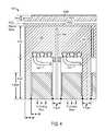
- FIG. 4illustrates a cross-sectional view of a portion of an electrostatic chuck configured to support a wafer or substrate, in accordance with another embodiment of the present invention.
- FIG. 5Aillustrates a cross-sectional view of a portion of an electrostatic chuck configured to support a wafer or substrate, highlighting a plasma spray arrangement, in accordance with another embodiment of the present invention.
- FIG. 5Billustrates a cross-sectional view of a portion of an electrostatic chuck configured to support a wafer or substrate, highlighting a solid ceramic top arrangement, in accordance with another embodiment of the present invention.
- FIG. 6is an electrical block-diagram including a 12 ⁇ 13 configuration of resistive auxiliary heaters for an electrostatic chuck (ESC), in accordance with various embodiments of the present invention.
- FIG. 7illustrates a system in which an electrostatic chuck with advanced RF and temperature uniformity can be housed, in accordance with an embodiment of the present invention.
- FIG. 8illustrates a block diagram of an exemplary computer system, in accordance with an embodiment of the present invention.
- Electrostatic chucks with advanced RF and temperature uniformity, and methods of fabricating such electrostatic chucksare described.
- numerous specific detailsare set forth, such as specific chuck material regimes, in order to provide a thorough understanding of embodiments of the present invention. It will be apparent to one skilled in the art that embodiments of the present invention may be practiced without these specific details. In other instances, well-known aspects, such as etch processing in the presence of a wafer supported by a chuck, are not described in detail in order to not unnecessarily obscure embodiments of the present invention.
- the various embodiments shown in the Figuresare illustrative representations and are not necessarily drawn to scale.
- One or more embodiments described hereinrelate to electrostatic chucks with advanced RF and temperature uniformity or systems including electrostatic chucks with advanced RF and temperature uniformity.
- wafer clampingby means of electrostatic chucking has been used to provide temperature control during etch processing.
- the waferis clamped to ceramic, or multi-layer surface with heat sink or heater (or both) depending on application.
- auxilary hardwaree.g., lifter pins, RF/DC electrodes, etc.
- the ceramic surface temperatureis not uniform. This non-uniformity translates to the wafer, affecting the etch process.
- Conventional chuck designshave concentrated on coolant layout optimization and introduction of multiple (up to 4 zones) heaters. Such chuck designs have not been useful for solving issue related to, or caused by, auxiliary hardware (e.g., lifter pins, RF/DC electrodes, etc.).
- next generation (beyond 4-zone) etch chamber ESC with extreme temperature uniformityis described.
- a chuck described hereincan achieve thermal requirements including one or more of Al 2 O 3 -based 12 inch puck, a temperature capability up to 130 C, temperature uniformity ⁇ 0.5 C at 65/65/45 degrees Celsius with plasma.
- Embodiments described hereinmay be directed to next generation etch chamber ESCs with active temperature control.
- FIGS. 1-5A and 5 Bdepict electrostatic (ESC) structures, or portions thereof, in accordance with various embodiments of the present invention.
- an ESC 100is configured to support a wafer or substrate 102 .
- a framework 104 of the ESCmay be composed of, e.g., aluminum.
- a plasma spray coat layer 106e.g., a ceramic layer, is included on various surfaces of the framework 104 .
- Main heaters 108are included, along with auxiliary heaters 110 .
- an ESC portion 200is configured to support a wafer or substrate 202 .
- a ceramic layer 204on which a wafer or substrate 202 is to reside, is disposed on a plurality of resistive heater elements 206 , e.g., and held in place by an adhesive layer 208 .
- a metal base 210supports the plurality of resistive heater elements 206 and may be RF hot.
- An optional chucking electrode 212may also be included, as depicted in FIG. 2 .
- a portion 220 of an ESC having a solid ceramic plate 221is provided to demonstrate RF pathways 222 and 224 within an ESC.
- An RF pathway 242is further demonstrated in portion 240 B of an ESC (which can also be configured as shown as 240 A), as is also shown from a cross-sectional perspective in FIG. 2 .
- the shown ESC portions 220 , 240 A and 240 Bcan be configured with a solid ceramic plate-only arrangement (as shown) or can include a plasma spray coat layer on which the solid ceramic plate is adhered, as described in greater detail below in association with FIG. 5B .
- an ESC 300is configured to support a wafer or substrate 302 .
- a dielectric layer 304e.g., a plasma spray dielectric layer, provides a support on which a wafer or substrate 302 is to reside.
- Open regions 306provide cooling channels, e.g., for backside helium (He) cooling.
- the dielectric layer 304is disposed above an upper metal portion 308 , e.g., which can provide a guide for RF waves.
- a dielectric layer 310e.g., a plasma spray or arc oxidation layer, is disposed above a plurality of pixilated resistive heaters 312 and is surrounded in part by the upper metal portion 308 .
- An additional dielectric layer 314is disposed below the dielectric layer 310 , with a boundary 316 between the dielectric layer 314 and the dielectric layer 310 .
- Vias 318are included to couple the plurality of pixilated resistive heaters 312 with a bus bar power distribution layer 320 .
- a dielectric layer 322is disposed below the bus bar power distribution layer 320 , with a boundary 324 between the dielectric layer 314 and the dielectric layer 322 .
- the above featuresare disposed above a metal base 326 .
- the metal base 326houses high power heater elements or boosters 328 .
- a welded bottom plate 330may also be included, as depicted in FIG. 3 .
- an electrostatic chuckhas 1 or more (up to 8) main heaters to provide baseline temperature control.
- main heatersTo provide fine-tuning of temperature distribution, a large number of auxiliary heaters is placed near ESC surface.
- all heatersare positioned inside aluminum cage, which acts as RF shield and RF delivery path at the same time.
- etch processingwith improved RF uniformity and/or improved temperature uniformity can be achieved.
- a chuck described hereincan achieve temperature uniformity requirements including one or more of: (1) for heater layout: RF coupling, process temperature ramp between steps, addressed with 4-zone heater design; (2) for tool matching: subtle variations in conventional ESC/showerhead/edge HW results in localized hot/cold spots and a multi-array, from 45 up to 169 equalization heaters are otherwise needed to match tool-to-tool temperature uniformity.
- the ESC 300 described in association with FIG. 3may be manufactured by first installing the high power heater elements or boosters 328 into the metal base 326 .
- the bottom plate 330is then welded into place.
- the dielectric layer 322is then deposited by, e.g., plasma spray or arc anodizing approaches.
- a metal layeris then formed, e.g., by screen printing, to provide bus bar power distribution layer 320 which can deliver current to the pixilated resistive heaters 312 .
- the dielectric layer 314is then deposited, covering the dielectric layer 324 . Via holes are then formed in the dielectric layer 314 , exposing the bus bar power distribution layer 320 .
- Metal depositionis then performed to fill the via holes, forming vias 318 .
- the vias 318may be filled while forming the pixilated resistive heaters 312 .
- Dielectric layer 310is then deposited, followed by deposition of the upper metal portion 308 .
- the upper metal portion 308is formed to provide edges of a metal base.
- Dielectric layer 304is then formed to cover all of the above described layers.
- featuresmay be machined into the dielectric layer 304 to tailor the wafer interface with ESC 300 .
- an ESC portion 400is configured to support a wafer or substrate.
- a top dielectric layer or feature of ESC 400may be provided by, e.g., including a deposited dielectric layer (e.g., Al 2 O 3 ) 402 A, e.g., by plasma spray.
- a dielectric plate 402 Bsuch as an Al 2 O 3 plate, may be included. Both options are depicted in FIG. 4 .
- a metal base 404such as an aluminum (Al) base, is included beneath the dielectric layer 402 A and/or the dielectric plate 402 B. Slots 406 may be included in the metal base 404 to provide a thermal break. Cable heaters 408 are housed in the metal base 404 .
- the metal base 404may further include pathways to a cooling base, as depicted in FIG. 4 .
- FIG. 5Adepicts an ESC portion 500 A, as shown from a cross-sectional perspective, highlighting the plasma spray configuration, in accordance with an embodiment of the present invention.
- ESC portion 500 Aincludes a metal base portion 502 , such as an aluminum base, with a plasma spray dielectric layer 504 disposed thereon.
- the plasma spray layermay be composed of a dielectric material such as, but not limited to, alumina (Al 2 O 3 ), yttrium oxide (Y 2 O 3 ) or a high performance material (HPM).
- a porous plug 506is disposed in the metal base portion 502 and provides a pathway 508 for wafer or substrate cooling, e.g., by helium flow.
- the pathway 508is disposed through the plasma spray dielectric layer 504 .
- FIG. 5Bdepicts an ESC portion 500 B, as shown from a cross-sectional perspective, highlighting the solid ceramic top configuration, in accordance with an embodiment of the present invention.
- ESC portion 500 Bincludes a metal base portion 552 , such as an aluminum base.
- a solid ceramic top 554(such as an Al 2 O 3 plate) is disposed above the metal base portion 552 .
- the solid ceramic top 554is disposed above a plasma spray dielectric layer 560 , as depicted in FIG. 5B .
- the plasma spray layer 560may be composed of a dielectric material such as, but not limited to, alumina (Al 2 O 3 ), yttrium oxide (Y 2 O 3 ) or a high performance material (HPM).
- the solid ceramic top 554may be coupled to the plasma spray dielectric layer 560 by an adhesive layer 562 .
- a porous plug 556is disposed in the metal base portion 552 and provides a pathway 558 for wafer or substrate cooling, e.g., by helium flow.
- the pathway 558is disposed through the solid ceramic top 554 and, if present, the plasma spray dielectric layer 560 .
- mechanical aspects of a chuck described hereininclude the ESC itself, a cathode assembly redesign for additional 24-26 filters, electrical, RF filters, power delivery to auxiliary heaters.
- commutation/switching logic aspects of a chuck described hereininclude interface with existing hardware.
- software aspects of a chuck described hereininclude interface with I-4 temperature data, and/or communication with electrical subassembly.
- a main heater for a chuck described hereinincludes a dual-zone heater.
- a power requirement for a chuck described hereinis addressed with auxiliary heaters.
- ESC type aspects of a chuck described hereininclude one or more of, coulombic, approximately 92% alumina composition, thin ceramic, possibly swappable/consumable, grounded cooling plates with RF-hot clamp electrode and/or printed RF electrode.
- a spec for max RF poweris approximately 2 kW max and approximately 13.56 MHz.
- a spec for max helium pressureis approximately 10 Torr.
- the RF current limitationsare quantified for pin-to-electrode interface of approximately 20 A per pin.
- inner/outer heater resistanceis approximately at 90 C, 130 C, 25 A, 160V, 150 C (inner) 13 A, 150V, 150 C (outer).
- auxiliary heaters for a chuck described hereininclude approximately 45 heaters, and up to 144-169 (12 ⁇ 12 or 13 ⁇ 13 configuration).
- An estimated power for the heaters at approximately 92% alumina, min localized 1 C heating, max 4° C. heating and 45 heatersis approximately 3 W for 6° C. delta between heaters (4 W hi-purity).
- feedbackincludes 2 sensors for dual-zone main heaters.
- RF filteringis based on 3 W average per heater, DC 294V, 1.75 Amp total for 169 heaters ( ⁇ 168 ⁇ ).
- FIG. 6is an electrical block-diagram 600 , in accordance with an embodiment of the present invention. Referring to FIG. 6 , a 12 ⁇ 13 configuration 602 of resistive auxiliary heaters is provided as an example.
- FIG. 7illustrates a system in which an electrostatic chuck with advanced RF and temperature uniformity can be housed, in accordance with an embodiment of the present invention.
- a system 700 for conducting a plasma etch processincludes a chamber 702 equipped with a sample holder 704 .
- An evacuation device 706 , a gas inlet device 708 and a plasma ignition device 710are coupled with chamber 702 .
- a computing device 712is coupled with plasma ignition device 710 .
- System 700may additionally include a voltage source 714 coupled with sample holder 704 and a detector 716 coupled with chamber 702 .
- Computing device 712may also be coupled with evacuation device 706 , gas inlet device 708 , voltage source 714 and detector 716 , as depicted in FIG. 7 .
- Chamber 702 and sample holder 704may include a reaction chamber and sample positioning device suitable to contain an ionized gas, i.e. a plasma, and bring a sample in proximity to the ionized gas or charged species ejected there from.
- Evacuation device 706may be a device suitable to evacuate and de-pressurize chamber 702 .
- Gas inlet device 708may be a device suitable to inject a reaction gas into chamber 702 .
- Plasma ignition device 710may be a device suitable for igniting a plasma derived from the reaction gas injected into chamber 702 by gas inlet device 708 .
- Detection device 716may be a device suitable to detect an end-point of a processing operation.
- system 700includes a chamber 702 , a sample holder 704 , an evacuation device 706 , a gas inlet device 708 , a plasma ignition device 710 and a detector 716 similar to, or the same as, a Conductor etch chamber or related chambers used on an Applied Materials® AdvantEdge system.
- Embodiments of the present inventionmay be provided as a computer program product, or software, that may include a machine-readable medium having stored thereon instructions, which may be used to program a computer system (or other electronic devices) to perform a process according to the present invention.
- a machine-readable mediumincludes any mechanism for storing or transmitting information in a form readable by a machine (e.g., a computer).
- a machine-readable (e.g., computer-readable) mediumincludes a machine (e.g., a computer) readable storage medium (e.g., read only memory (“ROM”), random access memory (“RAM”), magnetic disk storage media, optical storage media, flash memory devices, etc.), a machine (e.g., computer) readable transmission medium (electrical, optical, acoustical or other form of propagated signals (e.g., infrared signals, digital signals, etc.)), etc.
- FIG. 8illustrates a diagrammatic representation of a machine in the exemplary form of a computer system 800 within which a set of instructions, for causing the machine to perform any one or more of the methodologies discussed herein, may be executed.
- the machinemay be connected (e.g., networked) to other machines in a Local Area Network (LAN), an intranet, an extranet, or the Internet.
- LANLocal Area Network
- the machinemay operate in the capacity of a server or a client machine in a client-server network environment, or as a peer machine in a peer-to-peer (or distributed) network environment.
- the machinemay be a personal computer (PC), a tablet PC, a set-top box (STB), a Personal Digital Assistant (PDA), a cellular telephone, a web appliance, a server, a network router, switch or bridge, or any machine capable of executing a set of instructions (sequential or otherwise) that specify actions to be taken by that machine.
- PCpersonal computer
- PDAPersonal Digital Assistant
- STBset-top box
- WPAPersonal Digital Assistant
- a cellular telephonea web appliance
- servere.g., a server
- network routere.g., switch or bridge
- computer system 800is suitable for use as computing device 712 described in association with FIG. 7 .
- the exemplary computer system 800includes a processor 802 , a main memory 804 (e.g., read-only memory (ROM), flash memory, dynamic random access memory (DRAM) such as synchronous DRAM (SDRAM) or Rambus DRAM (RDRAM), etc.), a static memory 806 (e.g., flash memory, static random access memory (SRAM), etc.), and a secondary memory 818 (e.g., a data storage device), which communicate with each other via a bus 830 .
- main memory 804e.g., read-only memory (ROM), flash memory, dynamic random access memory (DRAM) such as synchronous DRAM (SDRAM) or Rambus DRAM (RDRAM), etc.
- DRAMdynamic random access memory
- SDRAMsynchronous DRAM
- RDRAMRambus DRAM
- static memory 806e.g., flash memory, static random access memory (SRAM), etc.
- secondary memory 818e.g., a data storage device
- Processor 802represents one or more general-purpose processing devices such as a microprocessor, central processing unit, or the like. More particularly, the processor 802 may be a complex instruction set computing (CISC) microprocessor, reduced instruction set computing (RISC) microprocessor, very long instruction word (VLIW) microprocessor, processor implementing other instruction sets, or processors implementing a combination of instruction sets. Processor 802 may also be one or more special-purpose processing devices such as an application specific integrated circuit (ASIC), a field programmable gate array (FPGA), a digital signal processor (DSP), network processor, or the like. Processor 802 is configured to execute the processing logic 826 for performing the operations discussed herein.
- CISCcomplex instruction set computing
- RISCreduced instruction set computing
- VLIWvery long instruction word
- Processor 802may also be one or more special-purpose processing devices such as an application specific integrated circuit (ASIC), a field programmable gate array (FPGA), a digital signal processor (DSP), network processor, or the like.
- the computer system 800may further include a network interface device 808 .
- the computer system 800also may include a video display unit 810 (e.g., a liquid crystal display (LCD) or a cathode ray tube (CRT)), an alphanumeric input device 812 (e.g., a keyboard), a cursor control device 814 (e.g., a mouse), and a signal generation device 816 (e.g., a speaker).
- a video display unit 810e.g., a liquid crystal display (LCD) or a cathode ray tube (CRT)
- an alphanumeric input device 812e.g., a keyboard
- a cursor control device 814e.g., a mouse
- a signal generation device 816e.g., a speaker
- the secondary memory 818may include a machine-accessible storage medium (or more specifically a computer-readable storage medium) 831 on which is stored one or more sets of instructions (e.g., software 822 ) embodying any one or more of the methodologies or functions described herein.
- the software 822may also reside, completely or at least partially, within the main memory 804 and/or within the processor 802 during execution thereof by the computer system 800 , the main memory 804 and the processor 802 also constituting machine-readable storage media.
- the software 822may further be transmitted or received over a network 820 via the network interface device 808 .
- machine-accessible storage medium 831is shown in an exemplary embodiment to be a single medium, the term “machine-readable storage medium” should be taken to include a single medium or multiple media (e.g., a centralized or distributed database, and/or associated caches and servers) that store the one or more sets of instructions.
- the term “machine-readable storage medium”shall also be taken to include any medium that is capable of storing or encoding a set of instructions for execution by the machine and that cause the machine to perform any one or more of the methodologies of the present invention.
- the term “machine-readable storage medium”shall accordingly be taken to include, but not be limited to, solid-state memories, and optical and magnetic media.
- an electrostatic chuck (ESC) with advanced RF and temperature uniformityincludes a top dielectric layer.
- An upper metal portionis disposed below the top dielectric layer.
- a second dielectric layeris disposed above a plurality of pixilated resistive heaters and surrounded in part by the upper metal portion.
- a third dielectric layeris disposed below the second dielectric layer, with a boundary between the third dielectric layer and the second dielectric layer.
- a plurality of viasis disposed in the third dielectric layer.
- a bus power bar distribution layeris disposed below and coupled to the plurality of vias.
- the plurality of viaselectrically couples the plurality of pixilated resistive heaters to the bus bar power distribution layer.
- a fourth dielectric layeris disposed below the bus bar power distribution layer, with a boundary between the fourth dielectric layer and the third dielectric layer.
- a metal baseis disposed below the fourth dielectric layer. The metal base includes a plurality of high power heater elements housed therein.
Landscapes
- Engineering & Computer Science (AREA)
- Physics & Mathematics (AREA)
- Microelectronics & Electronic Packaging (AREA)
- General Physics & Mathematics (AREA)
- Manufacturing & Machinery (AREA)
- Computer Hardware Design (AREA)
- Condensed Matter Physics & Semiconductors (AREA)
- Power Engineering (AREA)
- Drying Of Semiconductors (AREA)
- Container, Conveyance, Adherence, Positioning, Of Wafer (AREA)
- Plasma & Fusion (AREA)
- Chemical & Material Sciences (AREA)
- Chemical Kinetics & Catalysis (AREA)
- Chemical Vapour Deposition (AREA)
Abstract
Description
This application claims the benefit of U.S. Provisional Application No. 61/637,500, filed Apr. 24, 2012, and U.S. Provisional Application No. 61/775,372, filed Mar. 8, 2013, the entire contents of which are hereby incorporated by reference herein.
1) Field
Embodiments of the present invention pertain to the field of semiconductor processing equipment and, in particular, to electrostatic chucks with advanced RF and temperature uniformity, and methods of fabricating such electrostatic chucks.
2) Description of Related Art
In a plasma processing chamber, such as a plasma etch or plasma deposition chamber, the temperature of a chamber component is often an important parameter to control during a process. For example, a temperature of a substrate holder, commonly called a chuck or pedestal, may be controlled to heat/cool a workpiece to various controlled temperatures during the process recipe (e.g., to control an etch rate). Similarly, a temperature of a showerhead/upper electrode, chamber liner, baffle, process kit, or other component may also be controlled during the process recipe to influence the processing. Conventionally, a heat sink and/or heat source is coupled to the processing chamber to maintain the temperature of a chamber component at a desired temperature. Often, at least one heat transfer fluid loop thermally coupled to the chamber component is utilized to provide heating and/or cooling power.
Long line lengths in a heat transfer fluid loop, and the large heat transfer fluid volumes associated with such long line lengths are detrimental to temperature control response times. Point-of-use systems are one means to reduce fluid loop lengths/volumes. However, physical space constraints disadvantageously limit the power loads of such point-of-use systems.
With plasma processing trends continuing to increase RF power levels and also increase workpiece diameters (with 300 mm now typical and 450 mm systems now under development), temperature and/or RF control and distribution addressing both a fast response time and high power loads is advantageous in the plasma processing field.
Electrostatic chucks with advanced RF and temperature uniformity, and methods of fabricating such electrostatic chucks, are described. In the following description, numerous specific details are set forth, such as specific chuck material regimes, in order to provide a thorough understanding of embodiments of the present invention. It will be apparent to one skilled in the art that embodiments of the present invention may be practiced without these specific details. In other instances, well-known aspects, such as etch processing in the presence of a wafer supported by a chuck, are not described in detail in order to not unnecessarily obscure embodiments of the present invention. Furthermore, it is to be understood that the various embodiments shown in the Figures are illustrative representations and are not necessarily drawn to scale.
One or more embodiments described herein relate to electrostatic chucks with advanced RF and temperature uniformity or systems including electrostatic chucks with advanced RF and temperature uniformity.
To provide context, wafer clamping by means of electrostatic chucking has been used to provide temperature control during etch processing. The wafer is clamped to ceramic, or multi-layer surface with heat sink or heater (or both) depending on application. Due to inherent non-uniformities and auxilary hardware (e.g., lifter pins, RF/DC electrodes, etc.) the ceramic surface temperature is not uniform. This non-uniformity translates to the wafer, affecting the etch process. Conventional chuck designs have concentrated on coolant layout optimization and introduction of multiple (up to 4 zones) heaters. Such chuck designs have not been useful for solving issue related to, or caused by, auxiliary hardware (e.g., lifter pins, RF/DC electrodes, etc.).
In an embodiment, in order to address the above described issues with conventional approaches, next generation (beyond 4-zone) etch chamber ESC with extreme temperature uniformity is described. In an embodiment, as described in greater detail below, a chuck described herein can achieve thermal requirements including one or more of Al2O3-based 12 inch puck, a temperature capability up to 130 C, temperature uniformity ≦0.5 C at 65/65/45 degrees Celsius with plasma. Embodiments described herein may be directed to next generation etch chamber ESCs with active temperature control.
Referring toFIG. 1 , anESC 100 is configured to support a wafer orsubstrate 102. Aframework 104 of the ESC may be composed of, e.g., aluminum. A plasmaspray coat layer 106, e.g., a ceramic layer, is included on various surfaces of theframework 104.Main heaters 108 are included, along withauxiliary heaters 110.
Referring toFIG. 2 , anESC portion 200, as shown from a cross-sectional perspective, is configured to support a wafer orsubstrate 202. Aceramic layer 204, on which a wafer orsubstrate 202 is to reside, is disposed on a plurality ofresistive heater elements 206, e.g., and held in place by anadhesive layer 208. Ametal base 210 supports the plurality ofresistive heater elements 206 and may be RF hot. Anoptional chucking electrode 212 may also be included, as depicted inFIG. 2 .
Referring again toFIG. 2 , aportion 220 of an ESC having a solidceramic plate 221, as shown from a cross-sectional perspective, is provided to demonstrateRF pathways RF pathway 242 is further demonstrated inportion 240B of an ESC (which can also be configured as shown as240A), as is also shown from a cross-sectional perspective inFIG. 2 . It is to be understood that in some embodiments, the shownESC portions FIG. 5B .
Referring toFIG. 3 , anESC 300, as shown from a cross-sectional perspective, is configured to support a wafer orsubstrate 302. Adielectric layer 304, e.g., a plasma spray dielectric layer, provides a support on which a wafer orsubstrate 302 is to reside.Open regions 306 provide cooling channels, e.g., for backside helium (He) cooling. Thedielectric layer 304 is disposed above anupper metal portion 308, e.g., which can provide a guide for RF waves. Adielectric layer 310, e.g., a plasma spray or arc oxidation layer, is disposed above a plurality of pixilatedresistive heaters 312 and is surrounded in part by theupper metal portion 308. An additionaldielectric layer 314 is disposed below thedielectric layer 310, with aboundary 316 between thedielectric layer 314 and thedielectric layer 310.Vias 318 are included to couple the plurality of pixilatedresistive heaters 312 with a bus barpower distribution layer 320. Adielectric layer 322 is disposed below the bus barpower distribution layer 320, with aboundary 324 between thedielectric layer 314 and thedielectric layer 322. The above features are disposed above ametal base 326. Themetal base 326 houses high power heater elements orboosters 328. A weldedbottom plate 330 may also be included, as depicted inFIG. 3 .
In accordance with an embodiment of the present invention, an electrostatic chuck (ESC) has 1 or more (up to 8) main heaters to provide baseline temperature control. To provide fine-tuning of temperature distribution, a large number of auxiliary heaters is placed near ESC surface. To reduce RF-related uniformity, all heaters are positioned inside aluminum cage, which acts as RF shield and RF delivery path at the same time. Thus, in an embodiment, etch processing with improved RF uniformity and/or improved temperature uniformity can be achieved.
In a particular embodiment, a chuck described herein can achieve temperature uniformity requirements including one or more of: (1) for heater layout: RF coupling, process temperature ramp between steps, addressed with 4-zone heater design; (2) for tool matching: subtle variations in conventional ESC/showerhead/edge HW results in localized hot/cold spots and a multi-array, from 45 up to 169 equalization heaters are otherwise needed to match tool-to-tool temperature uniformity.
In an embodiment, theESC 300 described in association withFIG. 3 may be manufactured by first installing the high power heater elements orboosters 328 into themetal base 326. Thebottom plate 330 is then welded into place. Thedielectric layer 322 is then deposited by, e.g., plasma spray or arc anodizing approaches. A metal layer is then formed, e.g., by screen printing, to provide bus barpower distribution layer 320 which can deliver current to the pixilatedresistive heaters 312. Thedielectric layer 314 is then deposited, covering thedielectric layer 324. Via holes are then formed in thedielectric layer 314, exposing the bus barpower distribution layer 320. Metal deposition is then performed to fill the via holes, formingvias 318. Alternatively, thevias 318 may be filled while forming the pixilatedresistive heaters 312.Dielectric layer 310 is then deposited, followed by deposition of theupper metal portion 308. Theupper metal portion 308 is formed to provide edges of a metal base.Dielectric layer 304 is then formed to cover all of the above described layers. Optionally, features may be machined into thedielectric layer 304 to tailor the wafer interface withESC 300.
Referring toFIG. 4 , anESC portion 400, as shown from a cross-sectional perspective, is configured to support a wafer or substrate. A top dielectric layer or feature ofESC 400 may be provided by, e.g., including a deposited dielectric layer (e.g., Al2O3)402A, e.g., by plasma spray. Alternatively, or in addition to, adielectric plate 402B, such as an Al2O3plate, may be included. Both options are depicted inFIG. 4 . Ametal base 404, such as an aluminum (Al) base, is included beneath the dielectric layer402A and/or thedielectric plate 402B.Slots 406 may be included in themetal base 404 to provide a thermal break.Cable heaters 408 are housed in themetal base 404. Themetal base 404 may further include pathways to a cooling base, as depicted inFIG. 4 .
In an embodiment, mechanical aspects of a chuck described herein include the ESC itself, a cathode assembly redesign for additional 24-26 filters, electrical, RF filters, power delivery to auxiliary heaters. In an embodiment, commutation/switching logic aspects of a chuck described herein include interface with existing hardware. In an embodiment, software aspects of a chuck described herein include interface with I-4 temperature data, and/or communication with electrical subassembly. In an embodiment, a main heater for a chuck described herein includes a dual-zone heater. In an embodiment, a power requirement for a chuck described herein is addressed with auxiliary heaters.
In an embodiment, ESC type aspects of a chuck described herein include one or more of, coulombic, approximately 92% alumina composition, thin ceramic, possibly swappable/consumable, grounded cooling plates with RF-hot clamp electrode and/or printed RF electrode. In an embodiment, a spec for max RF power is approximately 2 kW max and approximately 13.56 MHz. In an embodiment, a spec for max helium pressure is approximately 10 Torr. In an embodiment, the RF current limitations are quantified for pin-to-electrode interface of approximately 20 A per pin. In an embodiment, inner/outer heater resistance is approximately at 90 C, 130 C, 25 A, 160V, 150 C (inner) 13 A, 150V, 150 C (outer).
In an embodiment, auxiliary heaters for a chuck described herein include approximately 45 heaters, and up to 144-169 (12×12 or 13×13 configuration). An estimated power for the heaters at approximately 92% alumina, min localized 1 C heating,max 4° C. heating and 45 heaters is approximately 3 W for 6° C. delta between heaters (4 W hi-purity). In an embodiment, feedback includes 2 sensors for dual-zone main heaters. In an embodiment, RF filtering is based on 3 W average per heater, DC 294V, 1.75 Amp total for 169 heaters (˜168Ω). As an example,FIG. 6 is an electrical block-diagram600, in accordance with an embodiment of the present invention. Referring toFIG. 6 , a 12×13 configuration602 of resistive auxiliary heaters is provided as an example.
An electrostatic chuck with advanced RF and temperature uniformity may be included in processing equipment suitable to provide an etch plasma in proximity to a sample for etching. For example,FIG. 7 illustrates a system in which an electrostatic chuck with advanced RF and temperature uniformity can be housed, in accordance with an embodiment of the present invention.
Referring toFIG. 7 , asystem 700 for conducting a plasma etch process includes achamber 702 equipped with asample holder 704. Anevacuation device 706, agas inlet device 708 and aplasma ignition device 710 are coupled withchamber 702. Acomputing device 712 is coupled withplasma ignition device 710.System 700 may additionally include avoltage source 714 coupled withsample holder 704 and adetector 716 coupled withchamber 702.Computing device 712 may also be coupled withevacuation device 706,gas inlet device 708,voltage source 714 anddetector 716, as depicted inFIG. 7 .
Embodiments of the present invention may be provided as a computer program product, or software, that may include a machine-readable medium having stored thereon instructions, which may be used to program a computer system (or other electronic devices) to perform a process according to the present invention. A machine-readable medium includes any mechanism for storing or transmitting information in a form readable by a machine (e.g., a computer). For example, a machine-readable (e.g., computer-readable) medium includes a machine (e.g., a computer) readable storage medium (e.g., read only memory (“ROM”), random access memory (“RAM”), magnetic disk storage media, optical storage media, flash memory devices, etc.), a machine (e.g., computer) readable transmission medium (electrical, optical, acoustical or other form of propagated signals (e.g., infrared signals, digital signals, etc.)), etc.
Theexemplary computer system 800 includes aprocessor 802, a main memory804 (e.g., read-only memory (ROM), flash memory, dynamic random access memory (DRAM) such as synchronous DRAM (SDRAM) or Rambus DRAM (RDRAM), etc.), a static memory806 (e.g., flash memory, static random access memory (SRAM), etc.), and a secondary memory818 (e.g., a data storage device), which communicate with each other via abus 830.
Thecomputer system 800 may further include anetwork interface device 808. Thecomputer system 800 also may include a video display unit810 (e.g., a liquid crystal display (LCD) or a cathode ray tube (CRT)), an alphanumeric input device812 (e.g., a keyboard), a cursor control device814 (e.g., a mouse), and a signal generation device816 (e.g., a speaker).
Thesecondary memory 818 may include a machine-accessible storage medium (or more specifically a computer-readable storage medium)831 on which is stored one or more sets of instructions (e.g., software822) embodying any one or more of the methodologies or functions described herein. Thesoftware 822 may also reside, completely or at least partially, within themain memory 804 and/or within theprocessor 802 during execution thereof by thecomputer system 800, themain memory 804 and theprocessor 802 also constituting machine-readable storage media. Thesoftware 822 may further be transmitted or received over anetwork 820 via thenetwork interface device 808.
While the machine-accessible storage medium 831 is shown in an exemplary embodiment to be a single medium, the term “machine-readable storage medium” should be taken to include a single medium or multiple media (e.g., a centralized or distributed database, and/or associated caches and servers) that store the one or more sets of instructions. The term “machine-readable storage medium” shall also be taken to include any medium that is capable of storing or encoding a set of instructions for execution by the machine and that cause the machine to perform any one or more of the methodologies of the present invention. The term “machine-readable storage medium” shall accordingly be taken to include, but not be limited to, solid-state memories, and optical and magnetic media.
Thus, electrostatic chucks with advanced RF and temperature uniformity, and methods of fabricating such electrostatic chucks, have been disclosed. In an embodiment, an electrostatic chuck (ESC) with advanced RF and temperature uniformity includes a top dielectric layer. An upper metal portion is disposed below the top dielectric layer. A second dielectric layer is disposed above a plurality of pixilated resistive heaters and surrounded in part by the upper metal portion. A third dielectric layer is disposed below the second dielectric layer, with a boundary between the third dielectric layer and the second dielectric layer. A plurality of vias is disposed in the third dielectric layer. A bus power bar distribution layer is disposed below and coupled to the plurality of vias. The plurality of vias electrically couples the plurality of pixilated resistive heaters to the bus bar power distribution layer. A fourth dielectric layer is disposed below the bus bar power distribution layer, with a boundary between the fourth dielectric layer and the third dielectric layer. A metal base is disposed below the fourth dielectric layer. The metal base includes a plurality of high power heater elements housed therein.
Claims (20)
1. An electrostatic chuck (ESC) with advanced RF and temperature uniformity, the ESC comprising:
a top dielectric layer;
an upper metal portion disposed below the top dielectric layer;
a second dielectric layer disposed above a plurality of pixilated resistive heaters and surrounded in part by the upper metal portion;
a third dielectric layer disposed below the second dielectric layer, with a boundary between the third dielectric layer and the second dielectric layer;
a plurality of vias disposed in the third dielectric layer;
a bus power bar distribution layer disposed below and coupled to the plurality of vias, wherein the plurality of vias electrically couple the plurality of pixilated resistive heaters to the bus bar power distribution layer;
a fourth dielectric layer disposed below the bus bar power distribution layer, with a boundary between the fourth dielectric layer and the third dielectric layer; and
a metal base disposed below the fourth dielectric layer, wherein the metal base comprises a plurality of high power heater elements housed therein.
2. The ESC ofclaim 1 , wherein the top dielectric layer comprises a plurality of surface features disposed therein.
3. The ESC ofclaim 2 , wherein the surface features of the top dielectric layer provide cooling channels for the ESC.
4. The ESC ofclaim 1 , wherein the top dielectric layer is configured for supporting a wafer or substrate thereon.
5. The ESC ofclaim 1 , wherein the top dielectric layer comprises a spray dielectric material.
6. The ESC ofclaim 1 , further comprising:
a solid ceramic plate disposed on the top dielectric layer.
7. The ESC ofclaim 6 , wherein the solid ceramic plate is configured for supporting a wafer or substrate thereon.
8. The ESC ofclaim 1 , wherein the upper metal portion provides a guide for radio frequency (RF) waves.
9. The ESC ofclaim 1 , further comprising:
a bottom plate disposed below and welded to the metal base.
10. A method of fabricating an electrostatic chuck (ESC), the method comprising:
installing high power heater elements into housings in a metal base;
welding a bottom plate to the metal base to house the high power heater elements therein;
forming a first dielectric layer on the metal base by plasma spray or arc anodizing;
forming a metal layer on the first dielectric layer and forming a bus bar power distribution layer from the metal layer;
forming a second dielectric layer on the bus bar power distribution layer and on exposed portions of the first dielectric layer;
forming via holes in the second dielectric layer, exposing the bus bar power distribution layer;
filling the via holes with metal to form a plurality of conductive vias;
forming a plurality of pixilated resistive heaters disposed above and electrically coupled to the plurality of conductive vias;
forming a third dielectric layer on the plurality pixilated resistive heaters;
forming an upper metal portion on, and partially surrounding, the third dielectric layer; and
forming a top dielectric layer on the upper metal portion.
11. The method ofclaim 10 , wherein forming the top dielectric layer comprises using a plasma spray technique.
12. The method ofclaim 10 , further comprising:
machining a plurality of surface features in a top surface of the top dielectric layer.
13. The method ofclaim 10 , further comprising:
adhering a solid ceramic plate to the top dielectric layer.
14. An etching system, comprising:
a chamber coupled to an evacuation device, a gas inlet device, a plasma ignition device, and a detector;
a computing device coupled with the plasma ignition device;
a voltage source coupled with a ample holder comprising an electrostatic chuck (ESC), the ESC disposed in the chamber and comprising:
a top dielectric layer;
an upper metal portion disposed below the top dielectric layer;
a second dielectric layer disposed above a plurality of pixilated resistive heaters and surrounded in part by the upper metal portion;
a third dielectric layer disposed below the second dielectric layer, with a boundary between the third dielectric layer and the second dielectric layer;
a plurality of vias disposed in the third dielectric layer;
a bus power bar distribution layer disposed below and coupled to the plurality of vias, wherein the plurality of vias electrically couple the plurality of pixilated resistive heaters to the bus bar power distribution layer;
a fourth dielectric layer disposed below the bus bar power distribution layer, with a boundary between the fourth dielectric layer and the third dielectric layer; and
a metal base disposed below the fourth dielectric layer, wherein the metal base comprises a plurality of high power heater elements housed therein.
15. The etching system ofclaim 14 , wherein the top dielectric layer of the ESC comprises a plurality of surface features disposed therein, wherein the surface features of the top dielectric layer provide cooling channels for the ESC.
16. The etching system ofclaim 14 , wherein the top dielectric layer of the ESC is configured for supporting a wafer or substrate thereon.
17. The etching system ofclaim 14 , wherein the top dielectric layer of the ESC comprises a spray dielectric material.
18. The etching system ofclaim 14 , the ESC further comprising:
a solid ceramic plate disposed on the top dielectric layer, wherein the solid ceramic plate is configured for supporting a wafer or substrate thereon.
19. The etching system ofclaim 14 , wherein the upper metal portion of the ESC provides a guide for radio frequency (RF) waves.
20. The etching system ofclaim 14 , the ESC further comprising:
a bottom plate disposed below and welded to the metal base of the ESC.
Priority Applications (10)
| Application Number | Priority Date | Filing Date | Title |
|---|---|---|---|
| US13/867,515US8937800B2 (en) | 2012-04-24 | 2013-04-22 | Electrostatic chuck with advanced RF and temperature uniformity |
| KR1020157036563AKR20160006239A (en) | 2012-04-24 | 2013-04-23 | Electrostatic chuck with advanced rf and temperature uniformity |
| JP2015509085AJP5938140B2 (en) | 2012-04-24 | 2013-04-23 | Electrostatic chuck with high RF and temperature uniformity |
| PCT/US2013/037849WO2013163220A1 (en) | 2012-04-24 | 2013-04-23 | Electrostatic chuck with advanced rf and temperature uniformity |
| CN201610056402.2ACN105515450B (en) | 2012-04-24 | 2013-04-23 | Electrostatic Chuck with Enhanced RF and Temperature Uniformity |
| CN201380021270.4ACN104247002B (en) | 2012-04-24 | 2013-04-23 | Electrostatic chuck with enhanced RF and temperature uniformity |
| KR1020147032750AKR101584538B1 (en) | 2012-04-24 | 2013-04-23 | Electrostatic chuck with advanced rf and temperature uniformity |
| KR1020187015705AKR101958018B1 (en) | 2012-04-24 | 2013-04-23 | Electrostatic chuck with advanced rf and temperature uniformity |
| TW102114636ATWI509732B (en) | 2012-04-24 | 2013-04-24 | Electrostatic chuck with advanced rf and temperature uniformity |
| JP2016022809AJP6290275B2 (en) | 2012-04-24 | 2016-02-09 | Electrostatic chuck with high RF and temperature uniformity |
Applications Claiming Priority (3)
| Application Number | Priority Date | Filing Date | Title |
|---|---|---|---|
| US201261637500P | 2012-04-24 | 2012-04-24 | |
| US201361775372P | 2013-03-08 | 2013-03-08 | |
| US13/867,515US8937800B2 (en) | 2012-04-24 | 2013-04-22 | Electrostatic chuck with advanced RF and temperature uniformity |
Publications (2)
| Publication Number | Publication Date |
|---|---|
| US20130279066A1 US20130279066A1 (en) | 2013-10-24 |
| US8937800B2true US8937800B2 (en) | 2015-01-20 |
Family
ID=49379898
Family Applications (1)
| Application Number | Title | Priority Date | Filing Date |
|---|---|---|---|
| US13/867,515Active2033-06-06US8937800B2 (en) | 2012-04-24 | 2013-04-22 | Electrostatic chuck with advanced RF and temperature uniformity |
Country Status (6)
| Country | Link |
|---|---|
| US (1) | US8937800B2 (en) |
| JP (2) | JP5938140B2 (en) |
| KR (3) | KR20160006239A (en) |
| CN (2) | CN104247002B (en) |
| TW (1) | TWI509732B (en) |
| WO (1) | WO2013163220A1 (en) |
Cited By (245)
| Publication number | Priority date | Publication date | Assignee | Title |
|---|---|---|---|---|
| US9472435B2 (en) | 2014-07-23 | 2016-10-18 | Applied Materials, Inc. | Tunable temperature controlled substrate support assembly |
| US9472410B2 (en) | 2014-03-05 | 2016-10-18 | Applied Materials, Inc. | Pixelated capacitance controlled ESC |
| US9520315B2 (en) | 2013-12-31 | 2016-12-13 | Applied Materials, Inc. | Electrostatic chuck with internal flow adjustments for improved temperature distribution |
| US9530988B2 (en)* | 2015-03-26 | 2016-12-27 | Samsung Display Co., Ltd. | Electrostatic chuck system and method of manufacturing organic light-emitting display apparatus by using the electrostatic chuck system |
| US9622375B2 (en) | 2013-12-31 | 2017-04-11 | Applied Materials, Inc. | Electrostatic chuck with external flow adjustments for improved temperature distribution |
| US9681497B2 (en) | 2013-03-12 | 2017-06-13 | Applied Materials, Inc. | Multi zone heating and cooling ESC for plasma process chamber |
| US10332772B2 (en) | 2013-03-13 | 2019-06-25 | Applied Materials, Inc. | Multi-zone heated ESC with independent edge zones |
| US10403534B2 (en) | 2013-11-11 | 2019-09-03 | Applied Materials, Inc. | Pixilated cooling, temperature controlled substrate support assembly |
| US10440777B2 (en) | 2015-05-22 | 2019-10-08 | Applied Materials, Inc. | Azimuthally tunable multi-zone electrostatic chuck |
| US10460968B2 (en) | 2013-12-02 | 2019-10-29 | Applied Materials, Inc. | Electrostatic chuck with variable pixelated magnetic field |
| US10685861B2 (en) | 2016-08-26 | 2020-06-16 | Applied Materials, Inc. | Direct optical heating of substrates through optical guide |
| US10736182B2 (en) | 2014-07-02 | 2020-08-04 | Applied Materials, Inc. | Apparatus, systems, and methods for temperature control of substrates using embedded fiber optics and epoxy optical diffusers |
| US10973088B2 (en) | 2016-04-18 | 2021-04-06 | Applied Materials, Inc. | Optically heated substrate support assembly with removable optical fibers |
| US20210101249A1 (en)* | 2015-12-10 | 2021-04-08 | Ioneer, LLC. | Apparatus and method for determining parameters of process operation |
| US11004710B2 (en)* | 2019-06-04 | 2021-05-11 | Applied Materials, Inc. | Wafer placement error detection based on measuring a current through an electrostatic chuck and solution for intervention |
| US11158526B2 (en) | 2014-02-07 | 2021-10-26 | Applied Materials, Inc. | Temperature controlled substrate support assembly |
| US11232963B2 (en)* | 2018-10-03 | 2022-01-25 | Asm Ip Holding B.V. | Substrate processing apparatus and method |
| US11274369B2 (en) | 2018-09-11 | 2022-03-15 | Asm Ip Holding B.V. | Thin film deposition method |
| US11286558B2 (en) | 2019-08-23 | 2022-03-29 | Asm Ip Holding B.V. | Methods for depositing a molybdenum nitride film on a surface of a substrate by a cyclical deposition process and related semiconductor device structures including a molybdenum nitride film |
| US11295980B2 (en) | 2017-08-30 | 2022-04-05 | Asm Ip Holding B.V. | Methods for depositing a molybdenum metal film over a dielectric surface of a substrate by a cyclical deposition process and related semiconductor device structures |
| US11296189B2 (en) | 2018-06-21 | 2022-04-05 | Asm Ip Holding B.V. | Method for depositing a phosphorus doped silicon arsenide film and related semiconductor device structures |
| USD947913S1 (en) | 2019-05-17 | 2022-04-05 | Asm Ip Holding B.V. | Susceptor shaft |
| US11306395B2 (en) | 2017-06-28 | 2022-04-19 | Asm Ip Holding B.V. | Methods for depositing a transition metal nitride film on a substrate by atomic layer deposition and related deposition apparatus |
| US11315794B2 (en) | 2019-10-21 | 2022-04-26 | Asm Ip Holding B.V. | Apparatus and methods for selectively etching films |
| US11342216B2 (en) | 2019-02-20 | 2022-05-24 | Asm Ip Holding B.V. | Cyclical deposition method and apparatus for filling a recess formed within a substrate surface |
| US11339476B2 (en) | 2019-10-08 | 2022-05-24 | Asm Ip Holding B.V. | Substrate processing device having connection plates, substrate processing method |
| US11345999B2 (en) | 2019-06-06 | 2022-05-31 | Asm Ip Holding B.V. | Method of using a gas-phase reactor system including analyzing exhausted gas |
| US11355338B2 (en) | 2019-05-10 | 2022-06-07 | Asm Ip Holding B.V. | Method of depositing material onto a surface and structure formed according to the method |
| US11361990B2 (en) | 2018-05-28 | 2022-06-14 | Asm Ip Holding B.V. | Substrate processing method and device manufactured by using the same |
| US11378337B2 (en) | 2019-03-28 | 2022-07-05 | Asm Ip Holding B.V. | Door opener and substrate processing apparatus provided therewith |
| US11387106B2 (en) | 2018-02-14 | 2022-07-12 | Asm Ip Holding B.V. | Method for depositing a ruthenium-containing film on a substrate by a cyclical deposition process |
| US11387120B2 (en) | 2017-09-28 | 2022-07-12 | Asm Ip Holding B.V. | Chemical dispensing apparatus and methods for dispensing a chemical to a reaction chamber |
| US11390945B2 (en) | 2019-07-03 | 2022-07-19 | Asm Ip Holding B.V. | Temperature control assembly for substrate processing apparatus and method of using same |
| US11390950B2 (en) | 2017-01-10 | 2022-07-19 | Asm Ip Holding B.V. | Reactor system and method to reduce residue buildup during a film deposition process |
| US11390946B2 (en) | 2019-01-17 | 2022-07-19 | Asm Ip Holding B.V. | Methods of forming a transition metal containing film on a substrate by a cyclical deposition process |
| US11393690B2 (en) | 2018-01-19 | 2022-07-19 | Asm Ip Holding B.V. | Deposition method |
| US11396702B2 (en) | 2016-11-15 | 2022-07-26 | Asm Ip Holding B.V. | Gas supply unit and substrate processing apparatus including the gas supply unit |
| US11398382B2 (en) | 2018-03-27 | 2022-07-26 | Asm Ip Holding B.V. | Method of forming an electrode on a substrate and a semiconductor device structure including an electrode |
| US11401605B2 (en) | 2019-11-26 | 2022-08-02 | Asm Ip Holding B.V. | Substrate processing apparatus |
| US11410851B2 (en) | 2017-02-15 | 2022-08-09 | Asm Ip Holding B.V. | Methods for forming a metallic film on a substrate by cyclical deposition and related semiconductor device structures |
| US11411088B2 (en) | 2018-11-16 | 2022-08-09 | Asm Ip Holding B.V. | Methods for forming a metal silicate film on a substrate in a reaction chamber and related semiconductor device structures |
| US11414760B2 (en) | 2018-10-08 | 2022-08-16 | Asm Ip Holding B.V. | Substrate support unit, thin film deposition apparatus including the same, and substrate processing apparatus including the same |
| US11417545B2 (en) | 2017-08-08 | 2022-08-16 | Asm Ip Holding B.V. | Radiation shield |
| US11424119B2 (en) | 2019-03-08 | 2022-08-23 | Asm Ip Holding B.V. | Method for selective deposition of silicon nitride layer and structure including selectively-deposited silicon nitride layer |
| US11430640B2 (en) | 2019-07-30 | 2022-08-30 | Asm Ip Holding B.V. | Substrate processing apparatus |
| US11430674B2 (en) | 2018-08-22 | 2022-08-30 | Asm Ip Holding B.V. | Sensor array, apparatus for dispensing a vapor phase reactant to a reaction chamber and related methods |
| US11437241B2 (en) | 2020-04-08 | 2022-09-06 | Asm Ip Holding B.V. | Apparatus and methods for selectively etching silicon oxide films |
| US11443926B2 (en) | 2019-07-30 | 2022-09-13 | Asm Ip Holding B.V. | Substrate processing apparatus |
| US11447861B2 (en) | 2016-12-15 | 2022-09-20 | Asm Ip Holding B.V. | Sequential infiltration synthesis apparatus and a method of forming a patterned structure |
| US11450529B2 (en) | 2019-11-26 | 2022-09-20 | Asm Ip Holding B.V. | Methods for selectively forming a target film on a substrate comprising a first dielectric surface and a second metallic surface |
| US11447864B2 (en) | 2019-04-19 | 2022-09-20 | Asm Ip Holding B.V. | Layer forming method and apparatus |
| USD965044S1 (en) | 2019-08-19 | 2022-09-27 | Asm Ip Holding B.V. | Susceptor shaft |
| US11453943B2 (en) | 2016-05-25 | 2022-09-27 | Asm Ip Holding B.V. | Method for forming carbon-containing silicon/metal oxide or nitride film by ALD using silicon precursor and hydrocarbon precursor |
| USD965524S1 (en) | 2019-08-19 | 2022-10-04 | Asm Ip Holding B.V. | Susceptor support |
| US11476109B2 (en) | 2019-06-11 | 2022-10-18 | Asm Ip Holding B.V. | Method of forming an electronic structure using reforming gas, system for performing the method, and structure formed using the method |
| US11473195B2 (en) | 2018-03-01 | 2022-10-18 | Asm Ip Holding B.V. | Semiconductor processing apparatus and a method for processing a substrate |
| US11482533B2 (en) | 2019-02-20 | 2022-10-25 | Asm Ip Holding B.V. | Apparatus and methods for plug fill deposition in 3-D NAND applications |
| US11482412B2 (en) | 2018-01-19 | 2022-10-25 | Asm Ip Holding B.V. | Method for depositing a gap-fill layer by plasma-assisted deposition |
| US11482418B2 (en) | 2018-02-20 | 2022-10-25 | Asm Ip Holding B.V. | Substrate processing method and apparatus |
| US11488854B2 (en) | 2020-03-11 | 2022-11-01 | Asm Ip Holding B.V. | Substrate handling device with adjustable joints |
| US11488819B2 (en) | 2018-12-04 | 2022-11-01 | Asm Ip Holding B.V. | Method of cleaning substrate processing apparatus |
| US11495459B2 (en) | 2019-09-04 | 2022-11-08 | Asm Ip Holding B.V. | Methods for selective deposition using a sacrificial capping layer |
| US11492703B2 (en) | 2018-06-27 | 2022-11-08 | Asm Ip Holding B.V. | Cyclic deposition methods for forming metal-containing material and films and structures including the metal-containing material |
| US11501973B2 (en) | 2018-01-16 | 2022-11-15 | Asm Ip Holding B.V. | Method for depositing a material film on a substrate within a reaction chamber by a cyclical deposition process and related device structures |
| US11501968B2 (en) | 2019-11-15 | 2022-11-15 | Asm Ip Holding B.V. | Method for providing a semiconductor device with silicon filled gaps |
| US11499222B2 (en) | 2018-06-27 | 2022-11-15 | Asm Ip Holding B.V. | Cyclic deposition methods for forming metal-containing material and films and structures including the metal-containing material |
| US11499226B2 (en) | 2018-11-02 | 2022-11-15 | Asm Ip Holding B.V. | Substrate supporting unit and a substrate processing device including the same |
| US11515188B2 (en) | 2019-05-16 | 2022-11-29 | Asm Ip Holding B.V. | Wafer boat handling device, vertical batch furnace and method |
| US11515187B2 (en) | 2020-05-01 | 2022-11-29 | Asm Ip Holding B.V. | Fast FOUP swapping with a FOUP handler |
| US11521851B2 (en) | 2020-02-03 | 2022-12-06 | Asm Ip Holding B.V. | Method of forming structures including a vanadium or indium layer |
| US11527403B2 (en) | 2019-12-19 | 2022-12-13 | Asm Ip Holding B.V. | Methods for filling a gap feature on a substrate surface and related semiconductor structures |
| US11530483B2 (en) | 2018-06-21 | 2022-12-20 | Asm Ip Holding B.V. | Substrate processing system |
| US11532757B2 (en) | 2016-10-27 | 2022-12-20 | Asm Ip Holding B.V. | Deposition of charge trapping layers |
| US11530876B2 (en) | 2020-04-24 | 2022-12-20 | Asm Ip Holding B.V. | Vertical batch furnace assembly comprising a cooling gas supply |
| US11551925B2 (en) | 2019-04-01 | 2023-01-10 | Asm Ip Holding B.V. | Method for manufacturing a semiconductor device |
| US11551912B2 (en) | 2020-01-20 | 2023-01-10 | Asm Ip Holding B.V. | Method of forming thin film and method of modifying surface of thin film |
| USD975665S1 (en) | 2019-05-17 | 2023-01-17 | Asm Ip Holding B.V. | Susceptor shaft |
| US11557474B2 (en) | 2019-07-29 | 2023-01-17 | Asm Ip Holding B.V. | Methods for selective deposition utilizing n-type dopants and/or alternative dopants to achieve high dopant incorporation |
| US11562901B2 (en) | 2019-09-25 | 2023-01-24 | Asm Ip Holding B.V. | Substrate processing method |
| US11572620B2 (en) | 2018-11-06 | 2023-02-07 | Asm Ip Holding B.V. | Methods for selectively depositing an amorphous silicon film on a substrate |
| US11581186B2 (en) | 2016-12-15 | 2023-02-14 | Asm Ip Holding B.V. | Sequential infiltration synthesis apparatus |
| US11587821B2 (en) | 2017-08-08 | 2023-02-21 | Asm Ip Holding B.V. | Substrate lift mechanism and reactor including same |
| US11587814B2 (en) | 2019-07-31 | 2023-02-21 | Asm Ip Holding B.V. | Vertical batch furnace assembly |
| US11587815B2 (en) | 2019-07-31 | 2023-02-21 | Asm Ip Holding B.V. | Vertical batch furnace assembly |
| USD979506S1 (en) | 2019-08-22 | 2023-02-28 | Asm Ip Holding B.V. | Insulator |
| US11594450B2 (en) | 2019-08-22 | 2023-02-28 | Asm Ip Holding B.V. | Method for forming a structure with a hole |
| US11594600B2 (en) | 2019-11-05 | 2023-02-28 | Asm Ip Holding B.V. | Structures with doped semiconductor layers and methods and systems for forming same |
| USD980814S1 (en) | 2021-05-11 | 2023-03-14 | Asm Ip Holding B.V. | Gas distributor for substrate processing apparatus |
| USD980813S1 (en) | 2021-05-11 | 2023-03-14 | Asm Ip Holding B.V. | Gas flow control plate for substrate processing apparatus |
| US11605528B2 (en) | 2019-07-09 | 2023-03-14 | Asm Ip Holding B.V. | Plasma device using coaxial waveguide, and substrate treatment method |
| US11610775B2 (en) | 2016-07-28 | 2023-03-21 | Asm Ip Holding B.V. | Method and apparatus for filling a gap |
| US11610774B2 (en) | 2019-10-02 | 2023-03-21 | Asm Ip Holding B.V. | Methods for forming a topographically selective silicon oxide film by a cyclical plasma-enhanced deposition process |
| USD981973S1 (en) | 2021-05-11 | 2023-03-28 | Asm Ip Holding B.V. | Reactor wall for substrate processing apparatus |
| US11615970B2 (en) | 2019-07-17 | 2023-03-28 | Asm Ip Holding B.V. | Radical assist ignition plasma system and method |
| US11615980B2 (en) | 2019-02-20 | 2023-03-28 | Asm Ip Holding B.V. | Method and apparatus for filling a recess formed within a substrate surface |
| US11626308B2 (en) | 2020-05-13 | 2023-04-11 | Asm Ip Holding B.V. | Laser alignment fixture for a reactor system |
| US11626316B2 (en) | 2019-11-20 | 2023-04-11 | Asm Ip Holding B.V. | Method of depositing carbon-containing material on a surface of a substrate, structure formed using the method, and system for forming the structure |
| US11629407B2 (en) | 2019-02-22 | 2023-04-18 | Asm Ip Holding B.V. | Substrate processing apparatus and method for processing substrates |
| US11637011B2 (en) | 2019-10-16 | 2023-04-25 | Asm Ip Holding B.V. | Method of topology-selective film formation of silicon oxide |
| US11637014B2 (en) | 2019-10-17 | 2023-04-25 | Asm Ip Holding B.V. | Methods for selective deposition of doped semiconductor material |
| US11639811B2 (en) | 2017-11-27 | 2023-05-02 | Asm Ip Holding B.V. | Apparatus including a clean mini environment |
| US11639548B2 (en) | 2019-08-21 | 2023-05-02 | Asm Ip Holding B.V. | Film-forming material mixed-gas forming device and film forming device |
| US11646184B2 (en) | 2019-11-29 | 2023-05-09 | Asm Ip Holding B.V. | Substrate processing apparatus |
| US11646205B2 (en) | 2019-10-29 | 2023-05-09 | Asm Ip Holding B.V. | Methods of selectively forming n-type doped material on a surface, systems for selectively forming n-type doped material, and structures formed using same |
| US11644758B2 (en) | 2020-07-17 | 2023-05-09 | Asm Ip Holding B.V. | Structures and methods for use in photolithography |
| US11646197B2 (en) | 2018-07-03 | 2023-05-09 | Asm Ip Holding B.V. | Method for depositing silicon-free carbon-containing film as gap-fill layer by pulse plasma-assisted deposition |
| US11646204B2 (en) | 2020-06-24 | 2023-05-09 | Asm Ip Holding B.V. | Method for forming a layer provided with silicon |
| US11643724B2 (en) | 2019-07-18 | 2023-05-09 | Asm Ip Holding B.V. | Method of forming structures using a neutral beam |
| US11649546B2 (en) | 2016-07-08 | 2023-05-16 | Asm Ip Holding B.V. | Organic reactants for atomic layer deposition |
| US11658029B2 (en) | 2018-12-14 | 2023-05-23 | Asm Ip Holding B.V. | Method of forming a device structure using selective deposition of gallium nitride and system for same |
| US11658035B2 (en) | 2020-06-30 | 2023-05-23 | Asm Ip Holding B.V. | Substrate processing method |
| US11664267B2 (en) | 2019-07-10 | 2023-05-30 | Asm Ip Holding B.V. | Substrate support assembly and substrate processing device including the same |
| US11664245B2 (en) | 2019-07-16 | 2023-05-30 | Asm Ip Holding B.V. | Substrate processing device |
| US11664199B2 (en) | 2018-10-19 | 2023-05-30 | Asm Ip Holding B.V. | Substrate processing apparatus and substrate processing method |
| US11674220B2 (en) | 2020-07-20 | 2023-06-13 | Asm Ip Holding B.V. | Method for depositing molybdenum layers using an underlayer |
| US11676812B2 (en) | 2016-02-19 | 2023-06-13 | Asm Ip Holding B.V. | Method for forming silicon nitride film selectively on top/bottom portions |
| US11680839B2 (en) | 2019-08-05 | 2023-06-20 | Asm Ip Holding B.V. | Liquid level sensor for a chemical source vessel |
| US11682572B2 (en) | 2017-11-27 | 2023-06-20 | Asm Ip Holdings B.V. | Storage device for storing wafer cassettes for use with a batch furnace |
| US11688603B2 (en) | 2019-07-17 | 2023-06-27 | Asm Ip Holding B.V. | Methods of forming silicon germanium structures |
| USD990534S1 (en) | 2020-09-11 | 2023-06-27 | Asm Ip Holding B.V. | Weighted lift pin |
| US11685991B2 (en) | 2018-02-14 | 2023-06-27 | Asm Ip Holding B.V. | Method for depositing a ruthenium-containing film on a substrate by a cyclical deposition process |
| USD990441S1 (en) | 2021-09-07 | 2023-06-27 | Asm Ip Holding B.V. | Gas flow control plate |
| US11694892B2 (en) | 2016-07-28 | 2023-07-04 | Asm Ip Holding B.V. | Method and apparatus for filling a gap |
| US11695054B2 (en) | 2017-07-18 | 2023-07-04 | Asm Ip Holding B.V. | Methods for forming a semiconductor device structure and related semiconductor device structures |
| US11705333B2 (en) | 2020-05-21 | 2023-07-18 | Asm Ip Holding B.V. | Structures including multiple carbon layers and methods of forming and using same |
| US11718913B2 (en) | 2018-06-04 | 2023-08-08 | Asm Ip Holding B.V. | Gas distribution system and reactor system including same |
| US11725280B2 (en) | 2020-08-26 | 2023-08-15 | Asm Ip Holding B.V. | Method for forming metal silicon oxide and metal silicon oxynitride layers |
| US11725277B2 (en) | 2011-07-20 | 2023-08-15 | Asm Ip Holding B.V. | Pressure transmitter for a semiconductor processing environment |
| US11735414B2 (en) | 2018-02-06 | 2023-08-22 | Asm Ip Holding B.V. | Method of post-deposition treatment for silicon oxide film |
| US11735445B2 (en) | 2018-10-31 | 2023-08-22 | Asm Ip Holding B.V. | Substrate processing apparatus for processing substrates |
| US11735422B2 (en) | 2019-10-10 | 2023-08-22 | Asm Ip Holding B.V. | Method of forming a photoresist underlayer and structure including same |
| US11742198B2 (en) | 2019-03-08 | 2023-08-29 | Asm Ip Holding B.V. | Structure including SiOCN layer and method of forming same |
| US11742189B2 (en) | 2015-03-12 | 2023-08-29 | Asm Ip Holding B.V. | Multi-zone reactor, system including the reactor, and method of using the same |
| US11749562B2 (en) | 2016-07-08 | 2023-09-05 | Asm Ip Holding B.V. | Selective deposition method to form air gaps |
| US11769682B2 (en) | 2017-08-09 | 2023-09-26 | Asm Ip Holding B.V. | Storage apparatus for storing cassettes for substrates and processing apparatus equipped therewith |
| US11769670B2 (en) | 2018-12-13 | 2023-09-26 | Asm Ip Holding B.V. | Methods for forming a rhenium-containing film on a substrate by a cyclical deposition process and related semiconductor device structures |
| US11767589B2 (en) | 2020-05-29 | 2023-09-26 | Asm Ip Holding B.V. | Substrate processing device |
| US11776846B2 (en) | 2020-02-07 | 2023-10-03 | Asm Ip Holding B.V. | Methods for depositing gap filling fluids and related systems and devices |
| US11781243B2 (en) | 2020-02-17 | 2023-10-10 | Asm Ip Holding B.V. | Method for depositing low temperature phosphorous-doped silicon |
| US11781221B2 (en) | 2019-05-07 | 2023-10-10 | Asm Ip Holding B.V. | Chemical source vessel with dip tube |
| US11795545B2 (en) | 2014-10-07 | 2023-10-24 | Asm Ip Holding B.V. | Multiple temperature range susceptor, assembly, reactor and system including the susceptor, and methods of using the same |
| US11804364B2 (en) | 2020-05-19 | 2023-10-31 | Asm Ip Holding B.V. | Substrate processing apparatus |
| US11804388B2 (en) | 2018-09-11 | 2023-10-31 | Asm Ip Holding B.V. | Substrate processing apparatus and method |
| US11802338B2 (en) | 2017-07-26 | 2023-10-31 | Asm Ip Holding B.V. | Chemical treatment, deposition and/or infiltration apparatus and method for using the same |
| US11810788B2 (en) | 2016-11-01 | 2023-11-07 | Asm Ip Holding B.V. | Methods for forming a transition metal niobium nitride film on a substrate by atomic layer deposition and related semiconductor device structures |
| US11814747B2 (en) | 2019-04-24 | 2023-11-14 | Asm Ip Holding B.V. | Gas-phase reactor system-with a reaction chamber, a solid precursor source vessel, a gas distribution system, and a flange assembly |
| US11823866B2 (en) | 2020-04-02 | 2023-11-21 | Asm Ip Holding B.V. | Thin film forming method |
| US11823876B2 (en) | 2019-09-05 | 2023-11-21 | Asm Ip Holding B.V. | Substrate processing apparatus |
| US11821078B2 (en) | 2020-04-15 | 2023-11-21 | Asm Ip Holding B.V. | Method for forming precoat film and method for forming silicon-containing film |
| US11828707B2 (en) | 2020-02-04 | 2023-11-28 | Asm Ip Holding B.V. | Method and apparatus for transmittance measurements of large articles |
| US11830738B2 (en) | 2020-04-03 | 2023-11-28 | Asm Ip Holding B.V. | Method for forming barrier layer and method for manufacturing semiconductor device |
| US11827981B2 (en) | 2020-10-14 | 2023-11-28 | Asm Ip Holding B.V. | Method of depositing material on stepped structure |
| US11830730B2 (en) | 2017-08-29 | 2023-11-28 | Asm Ip Holding B.V. | Layer forming method and apparatus |
| US11840761B2 (en) | 2019-12-04 | 2023-12-12 | Asm Ip Holding B.V. | Substrate processing apparatus |
| US11848200B2 (en) | 2017-05-08 | 2023-12-19 | Asm Ip Holding B.V. | Methods for selectively forming a silicon nitride film on a substrate and related semiconductor device structures |
| US11873557B2 (en) | 2020-10-22 | 2024-01-16 | Asm Ip Holding B.V. | Method of depositing vanadium metal |
| US11876008B2 (en) | 2019-07-31 | 2024-01-16 | Asm Ip Holding B.V. | Vertical batch furnace assembly |
| US11876356B2 (en) | 2020-03-11 | 2024-01-16 | Asm Ip Holding B.V. | Lockout tagout assembly and system and method of using same |
| US11885020B2 (en) | 2020-12-22 | 2024-01-30 | Asm Ip Holding B.V. | Transition metal deposition method |
| US11887857B2 (en) | 2020-04-24 | 2024-01-30 | Asm Ip Holding B.V. | Methods and systems for depositing a layer comprising vanadium, nitrogen, and a further element |
| US11885023B2 (en) | 2018-10-01 | 2024-01-30 | Asm Ip Holding B.V. | Substrate retaining apparatus, system including the apparatus, and method of using same |
| US11885013B2 (en) | 2019-12-17 | 2024-01-30 | Asm Ip Holding B.V. | Method of forming vanadium nitride layer and structure including the vanadium nitride layer |
| USD1012873S1 (en) | 2020-09-24 | 2024-01-30 | Asm Ip Holding B.V. | Electrode for semiconductor processing apparatus |
| US11891696B2 (en) | 2020-11-30 | 2024-02-06 | Asm Ip Holding B.V. | Injector configured for arrangement within a reaction chamber of a substrate processing apparatus |
| US11898243B2 (en) | 2020-04-24 | 2024-02-13 | Asm Ip Holding B.V. | Method of forming vanadium nitride-containing layer |
| US11901179B2 (en) | 2020-10-28 | 2024-02-13 | Asm Ip Holding B.V. | Method and device for depositing silicon onto substrates |
| US11923190B2 (en) | 2018-07-03 | 2024-03-05 | Asm Ip Holding B.V. | Method for depositing silicon-free carbon-containing film as gap-fill layer by pulse plasma-assisted deposition |
| US11923181B2 (en) | 2019-11-29 | 2024-03-05 | Asm Ip Holding B.V. | Substrate processing apparatus for minimizing the effect of a filling gas during substrate processing |
| US11929251B2 (en) | 2019-12-02 | 2024-03-12 | Asm Ip Holding B.V. | Substrate processing apparatus having electrostatic chuck and substrate processing method |
| US11939673B2 (en) | 2018-02-23 | 2024-03-26 | Asm Ip Holding B.V. | Apparatus for detecting or monitoring for a chemical precursor in a high temperature environment |
| US11946137B2 (en) | 2020-12-16 | 2024-04-02 | Asm Ip Holding B.V. | Runout and wobble measurement fixtures |
| US11956977B2 (en) | 2015-12-29 | 2024-04-09 | Asm Ip Holding B.V. | Atomic layer deposition of III-V compounds to form V-NAND devices |
| US11959168B2 (en) | 2020-04-29 | 2024-04-16 | Asm Ip Holding B.V. | Solid source precursor vessel |
| US11961741B2 (en) | 2020-03-12 | 2024-04-16 | Asm Ip Holding B.V. | Method for fabricating layer structure having target topological profile |
| US11967488B2 (en) | 2013-02-01 | 2024-04-23 | Asm Ip Holding B.V. | Method for treatment of deposition reactor |
| USD1023959S1 (en) | 2021-05-11 | 2024-04-23 | Asm Ip Holding B.V. | Electrode for substrate processing apparatus |
| US11976359B2 (en) | 2020-01-06 | 2024-05-07 | Asm Ip Holding B.V. | Gas supply assembly, components thereof, and reactor system including same |
| US11986868B2 (en) | 2020-02-28 | 2024-05-21 | Asm Ip Holding B.V. | System dedicated for parts cleaning |
| US11987881B2 (en) | 2020-05-22 | 2024-05-21 | Asm Ip Holding B.V. | Apparatus for depositing thin films using hydrogen peroxide |
| US11993847B2 (en) | 2020-01-08 | 2024-05-28 | Asm Ip Holding B.V. | Injector |
| US11996309B2 (en) | 2019-05-16 | 2024-05-28 | Asm Ip Holding B.V. | Wafer boat handling device, vertical batch furnace and method |
| US11996292B2 (en) | 2019-10-25 | 2024-05-28 | Asm Ip Holding B.V. | Methods for filling a gap feature on a substrate surface and related semiconductor structures |
| US11996289B2 (en) | 2020-04-16 | 2024-05-28 | Asm Ip Holding B.V. | Methods of forming structures including silicon germanium and silicon layers, devices formed using the methods, and systems for performing the methods |
| US12009224B2 (en) | 2020-09-29 | 2024-06-11 | Asm Ip Holding B.V. | Apparatus and method for etching metal nitrides |
| US12009241B2 (en) | 2019-10-14 | 2024-06-11 | Asm Ip Holding B.V. | Vertical batch furnace assembly with detector to detect cassette |
| US12006572B2 (en) | 2019-10-08 | 2024-06-11 | Asm Ip Holding B.V. | Reactor system including a gas distribution assembly for use with activated species and method of using same |
| US12020934B2 (en) | 2020-07-08 | 2024-06-25 | Asm Ip Holding B.V. | Substrate processing method |
| US12027365B2 (en) | 2020-11-24 | 2024-07-02 | Asm Ip Holding B.V. | Methods for filling a gap and related systems and devices |
| US12025484B2 (en) | 2018-05-08 | 2024-07-02 | Asm Ip Holding B.V. | Thin film forming method |
| US12033885B2 (en) | 2020-01-06 | 2024-07-09 | Asm Ip Holding B.V. | Channeled lift pin |
| US12033849B2 (en) | 2019-08-23 | 2024-07-09 | Asm Ip Holding B.V. | Method for depositing silicon oxide film having improved quality by PEALD using bis(diethylamino)silane |
| US12033861B2 (en) | 2017-10-05 | 2024-07-09 | Asm Ip Holding B.V. | Method for selectively depositing a metallic film on a substrate |
| US12040200B2 (en) | 2017-06-20 | 2024-07-16 | Asm Ip Holding B.V. | Semiconductor processing apparatus and methods for calibrating a semiconductor processing apparatus |
| US12040177B2 (en) | 2020-08-18 | 2024-07-16 | Asm Ip Holding B.V. | Methods for forming a laminate film by cyclical plasma-enhanced deposition processes |
| US12040184B2 (en) | 2017-10-30 | 2024-07-16 | Asm Ip Holding B.V. | Methods for forming a semiconductor structure and related semiconductor structures |
| US12040199B2 (en) | 2018-11-28 | 2024-07-16 | Asm Ip Holding B.V. | Substrate processing apparatus for processing substrates |
| US12051602B2 (en) | 2020-05-04 | 2024-07-30 | Asm Ip Holding B.V. | Substrate processing system for processing substrates with an electronics module located behind a door in a front wall of the substrate processing system |
| US12051567B2 (en) | 2020-10-07 | 2024-07-30 | Asm Ip Holding B.V. | Gas supply unit and substrate processing apparatus including gas supply unit |
| US12057314B2 (en) | 2020-05-15 | 2024-08-06 | Asm Ip Holding B.V. | Methods for silicon germanium uniformity control using multiple precursors |
| US12068154B2 (en) | 2020-04-13 | 2024-08-20 | Asm Ip Holding B.V. | Method of forming a nitrogen-containing carbon film and system for performing the method |
| US12074022B2 (en) | 2020-08-27 | 2024-08-27 | Asm Ip Holding B.V. | Method and system for forming patterned structures using multiple patterning process |
| US12087586B2 (en) | 2020-04-15 | 2024-09-10 | Asm Ip Holding B.V. | Method of forming chromium nitride layer and structure including the chromium nitride layer |
| US12106944B2 (en) | 2020-06-02 | 2024-10-01 | Asm Ip Holding B.V. | Rotating substrate support |
| US12107005B2 (en) | 2020-10-06 | 2024-10-01 | Asm Ip Holding B.V. | Deposition method and an apparatus for depositing a silicon-containing material |
| US12112940B2 (en) | 2019-07-19 | 2024-10-08 | Asm Ip Holding B.V. | Method of forming topology-controlled amorphous carbon polymer film |
| US12125700B2 (en) | 2020-01-16 | 2024-10-22 | Asm Ip Holding B.V. | Method of forming high aspect ratio features |
| US12129545B2 (en) | 2020-12-22 | 2024-10-29 | Asm Ip Holding B.V. | Precursor capsule, a vessel and a method |
| US12131885B2 (en) | 2020-12-22 | 2024-10-29 | Asm Ip Holding B.V. | Plasma treatment device having matching box |
| US12148609B2 (en) | 2020-09-16 | 2024-11-19 | Asm Ip Holding B.V. | Silicon oxide deposition method |
| US12154824B2 (en) | 2020-08-14 | 2024-11-26 | Asm Ip Holding B.V. | Substrate processing method |
| US12159788B2 (en) | 2020-12-14 | 2024-12-03 | Asm Ip Holding B.V. | Method of forming structures for threshold voltage control |
| US12169361B2 (en) | 2019-07-30 | 2024-12-17 | Asm Ip Holding B.V. | Substrate processing apparatus and method |
| US12173402B2 (en) | 2018-02-15 | 2024-12-24 | Asm Ip Holding B.V. | Method of forming a transition metal containing film on a substrate by a cyclical deposition process, a method for supplying a transition metal halide compound to a reaction chamber, and related vapor deposition apparatus |
| US12173404B2 (en) | 2020-03-17 | 2024-12-24 | Asm Ip Holding B.V. | Method of depositing epitaxial material, structure formed using the method, and system for performing the method |
| US12195852B2 (en) | 2020-11-23 | 2025-01-14 | Asm Ip Holding B.V. | Substrate processing apparatus with an injector |
| US12203166B2 (en) | 2020-05-07 | 2025-01-21 | Asm Ip Holding B.V. | Apparatus and methods for performing an in-situ etch of reaction chambers with fluorine-based radicals |
| US12209308B2 (en) | 2020-11-12 | 2025-01-28 | Asm Ip Holding B.V. | Reactor and related methods |
| US12218000B2 (en) | 2020-09-25 | 2025-02-04 | Asm Ip Holding B.V. | Semiconductor processing method |
| US12217946B2 (en) | 2020-10-15 | 2025-02-04 | Asm Ip Holding B.V. | Method of manufacturing semiconductor device, and substrate treatment apparatus using ether-CAT |
| US12218269B2 (en) | 2020-02-13 | 2025-02-04 | Asm Ip Holding B.V. | Substrate processing apparatus including light receiving device and calibration method of light receiving device |
| US12217954B2 (en) | 2020-08-25 | 2025-02-04 | Asm Ip Holding B.V. | Method of cleaning a surface |
| USD1060598S1 (en) | 2021-12-03 | 2025-02-04 | Asm Ip Holding B.V. | Split showerhead cover |
| US12221357B2 (en) | 2020-04-24 | 2025-02-11 | Asm Ip Holding B.V. | Methods and apparatus for stabilizing vanadium compounds |
| US12230531B2 (en) | 2018-04-09 | 2025-02-18 | Asm Ip Holding B.V. | Substrate supporting apparatus, substrate processing apparatus including the same, and substrate processing method |
| US12240760B2 (en) | 2016-03-18 | 2025-03-04 | Asm Ip Holding B.V. | Aligned carbon nanotubes |
| US12243742B2 (en) | 2020-04-21 | 2025-03-04 | Asm Ip Holding B.V. | Method for processing a substrate |
| US12241158B2 (en) | 2020-07-20 | 2025-03-04 | Asm Ip Holding B.V. | Method for forming structures including transition metal layers |
| US12243757B2 (en) | 2020-05-21 | 2025-03-04 | Asm Ip Holding B.V. | Flange and apparatus for processing substrates |
| US12243747B2 (en) | 2020-04-24 | 2025-03-04 | Asm Ip Holding B.V. | Methods of forming structures including vanadium boride and vanadium phosphide layers |
| US12247286B2 (en) | 2019-08-09 | 2025-03-11 | Asm Ip Holding B.V. | Heater assembly including cooling apparatus and method of using same |
| US12255053B2 (en) | 2020-12-10 | 2025-03-18 | Asm Ip Holding B.V. | Methods and systems for depositing a layer |
| US12252785B2 (en) | 2019-06-10 | 2025-03-18 | Asm Ip Holding B.V. | Method for cleaning quartz epitaxial chambers |
| US12266524B2 (en) | 2020-06-16 | 2025-04-01 | Asm Ip Holding B.V. | Method for depositing boron containing silicon germanium layers |
| US12272527B2 (en) | 2018-05-09 | 2025-04-08 | Asm Ip Holding B.V. | Apparatus for use with hydrogen radicals and method of using same |
| US12276023B2 (en) | 2017-08-04 | 2025-04-15 | Asm Ip Holding B.V. | Showerhead assembly for distributing a gas within a reaction chamber |
| US12278129B2 (en) | 2020-03-04 | 2025-04-15 | Asm Ip Holding B.V. | Alignment fixture for a reactor system |
| US12288710B2 (en) | 2020-12-18 | 2025-04-29 | Asm Ip Holding B.V. | Wafer processing apparatus with a rotatable table |
| US12322591B2 (en) | 2020-07-27 | 2025-06-03 | Asm Ip Holding B.V. | Thin film deposition process |
| US12363960B2 (en) | 2017-07-19 | 2025-07-15 | Asm Ip Holding B.V. | Method for depositing a Group IV semiconductor and related semiconductor device structures |
| US12378665B2 (en) | 2018-10-26 | 2025-08-05 | Asm Ip Holding B.V. | High temperature coatings for a preclean and etch apparatus and related methods |
| US12406846B2 (en) | 2020-05-26 | 2025-09-02 | Asm Ip Holding B.V. | Method for depositing boron and gallium containing silicon germanium layers |
| US12410515B2 (en) | 2020-01-29 | 2025-09-09 | Asm Ip Holding B.V. | Contaminant trap system for a reactor system |
| US12428726B2 (en) | 2019-10-08 | 2025-09-30 | Asm Ip Holding B.V. | Gas injection system and reactor system including same |
| US12431334B2 (en) | 2020-02-13 | 2025-09-30 | Asm Ip Holding B.V. | Gas distribution assembly |
| US12444599B2 (en) | 2021-12-08 | 2025-10-14 | Asm Ip Holding B.V. | Method for forming an ultraviolet radiation responsive metal oxide-containing film |
Families Citing this family (125)
| Publication number | Priority date | Publication date | Assignee | Title |
|---|---|---|---|---|
| US9338871B2 (en) | 2010-01-29 | 2016-05-10 | Applied Materials, Inc. | Feedforward temperature control for plasma processing apparatus |
| US8916793B2 (en) | 2010-06-08 | 2014-12-23 | Applied Materials, Inc. | Temperature control in plasma processing apparatus using pulsed heat transfer fluid flow |
| US9324576B2 (en) | 2010-05-27 | 2016-04-26 | Applied Materials, Inc. | Selective etch for silicon films |
| US10283321B2 (en) | 2011-01-18 | 2019-05-07 | Applied Materials, Inc. | Semiconductor processing system and methods using capacitively coupled plasma |
| US9064815B2 (en) | 2011-03-14 | 2015-06-23 | Applied Materials, Inc. | Methods for etch of metal and metal-oxide films |
| US8999856B2 (en) | 2011-03-14 | 2015-04-07 | Applied Materials, Inc. | Methods for etch of sin films |
| US10274270B2 (en) | 2011-10-27 | 2019-04-30 | Applied Materials, Inc. | Dual zone common catch heat exchanger/chiller |
| US9267739B2 (en) | 2012-07-18 | 2016-02-23 | Applied Materials, Inc. | Pedestal with multi-zone temperature control and multiple purge capabilities |
| US9373517B2 (en) | 2012-08-02 | 2016-06-21 | Applied Materials, Inc. | Semiconductor processing with DC assisted RF power for improved control |
| US9132436B2 (en) | 2012-09-21 | 2015-09-15 | Applied Materials, Inc. | Chemical control features in wafer process equipment |
| US9299574B2 (en) | 2013-01-25 | 2016-03-29 | Applied Materials, Inc. | Silicon dioxide-polysilicon multi-layered stack etching with plasma etch chamber employing non-corrosive etchants |
| US9129911B2 (en) | 2013-01-31 | 2015-09-08 | Applied Materials, Inc. | Boron-doped carbon-based hardmask etch processing |
| US10256079B2 (en) | 2013-02-08 | 2019-04-09 | Applied Materials, Inc. | Semiconductor processing systems having multiple plasma configurations |
| US9362130B2 (en) | 2013-03-01 | 2016-06-07 | Applied Materials, Inc. | Enhanced etching processes using remote plasma sources |
| US20140271097A1 (en) | 2013-03-15 | 2014-09-18 | Applied Materials, Inc. | Processing systems and methods for halide scavenging |
| US9773648B2 (en) | 2013-08-30 | 2017-09-26 | Applied Materials, Inc. | Dual discharge modes operation for remote plasma |
| US9576809B2 (en) | 2013-11-04 | 2017-02-21 | Applied Materials, Inc. | Etch suppression with germanium |
| US9520303B2 (en) | 2013-11-12 | 2016-12-13 | Applied Materials, Inc. | Aluminum selective etch |
| US9101038B2 (en) | 2013-12-20 | 2015-08-04 | Lam Research Corporation | Electrostatic chuck including declamping electrode and method of declamping |
| US9299537B2 (en) | 2014-03-20 | 2016-03-29 | Applied Materials, Inc. | Radial waveguide systems and methods for post-match control of microwaves |
| US9903020B2 (en) | 2014-03-31 | 2018-02-27 | Applied Materials, Inc. | Generation of compact alumina passivation layers on aluminum plasma equipment components |
| US9309598B2 (en) | 2014-05-28 | 2016-04-12 | Applied Materials, Inc. | Oxide and metal removal |
| WO2015192256A1 (en) | 2014-06-17 | 2015-12-23 | Evatec Ag | Electro-static chuck with radiofrequency shunt |
| US9496167B2 (en) | 2014-07-31 | 2016-11-15 | Applied Materials, Inc. | Integrated bit-line airgap formation and gate stack post clean |
| US9659753B2 (en) | 2014-08-07 | 2017-05-23 | Applied Materials, Inc. | Grooved insulator to reduce leakage current |
| JP6868553B2 (en)* | 2014-08-15 | 2021-05-12 | アプライド マテリアルズ インコーポレイテッドApplied Materials,Incorporated | Methods and equipment for processing wafers with compressive or tensile stress at high temperatures in a plasma chemical vapor deposition system |
| US9553102B2 (en) | 2014-08-19 | 2017-01-24 | Applied Materials, Inc. | Tungsten separation |
| US9613822B2 (en) | 2014-09-25 | 2017-04-04 | Applied Materials, Inc. | Oxide etch selectivity enhancement |
| US9966240B2 (en) | 2014-10-14 | 2018-05-08 | Applied Materials, Inc. | Systems and methods for internal surface conditioning assessment in plasma processing equipment |
| US9355922B2 (en) | 2014-10-14 | 2016-05-31 | Applied Materials, Inc. | Systems and methods for internal surface conditioning in plasma processing equipment |
| US10002782B2 (en)* | 2014-10-17 | 2018-06-19 | Lam Research Corporation | ESC assembly including an electrically conductive gasket for uniform RF power delivery therethrough |
| US11637002B2 (en) | 2014-11-26 | 2023-04-25 | Applied Materials, Inc. | Methods and systems to enhance process uniformity |
| KR102288349B1 (en) | 2014-12-09 | 2021-08-11 | 삼성디스플레이 주식회사 | Electrostatic chuck system and method for manufacturing organic light emitting display device using the same |
| US10224210B2 (en) | 2014-12-09 | 2019-03-05 | Applied Materials, Inc. | Plasma processing system with direct outlet toroidal plasma source |
| US10573496B2 (en) | 2014-12-09 | 2020-02-25 | Applied Materials, Inc. | Direct outlet toroidal plasma source |
| US11257693B2 (en) | 2015-01-09 | 2022-02-22 | Applied Materials, Inc. | Methods and systems to improve pedestal temperature control |
| JP5962833B2 (en)* | 2015-01-16 | 2016-08-03 | Toto株式会社 | Electrostatic chuck |
| US20160225652A1 (en) | 2015-02-03 | 2016-08-04 | Applied Materials, Inc. | Low temperature chuck for plasma processing systems |
| US9728437B2 (en) | 2015-02-03 | 2017-08-08 | Applied Materials, Inc. | High temperature chuck for plasma processing systems |
| US9881805B2 (en) | 2015-03-02 | 2018-01-30 | Applied Materials, Inc. | Silicon selective removal |
| US9779974B2 (en)* | 2015-06-22 | 2017-10-03 | Lam Research Corporation | System and method for reducing temperature transition in an electrostatic chuck |
| JP2017028111A (en)* | 2015-07-23 | 2017-02-02 | 株式会社日立ハイテクノロジーズ | Plasma processing equipment |
| US9691645B2 (en)* | 2015-08-06 | 2017-06-27 | Applied Materials, Inc. | Bolted wafer chuck thermal management systems and methods for wafer processing systems |
| US9741593B2 (en) | 2015-08-06 | 2017-08-22 | Applied Materials, Inc. | Thermal management systems and methods for wafer processing systems |
| TWI808334B (en)* | 2015-08-06 | 2023-07-11 | 美商應用材料股份有限公司 | Workpiece holder |
| US9349605B1 (en) | 2015-08-07 | 2016-05-24 | Applied Materials, Inc. | Oxide etch selectivity systems and methods |
| US10504700B2 (en) | 2015-08-27 | 2019-12-10 | Applied Materials, Inc. | Plasma etching systems and methods with secondary plasma injection |
| US10186437B2 (en)* | 2015-10-05 | 2019-01-22 | Lam Research Corporation | Substrate holder having integrated temperature measurement electrical devices |
| WO2017066873A1 (en)* | 2015-10-19 | 2017-04-27 | Novena Tec Inc. | Process monitoring device |
| US10522371B2 (en) | 2016-05-19 | 2019-12-31 | Applied Materials, Inc. | Systems and methods for improved semiconductor etching and component protection |
| US10504754B2 (en) | 2016-05-19 | 2019-12-10 | Applied Materials, Inc. | Systems and methods for improved semiconductor etching and component protection |
| US9865484B1 (en) | 2016-06-29 | 2018-01-09 | Applied Materials, Inc. | Selective etch using material modification and RF pulsing |
| JP6238097B1 (en)* | 2016-07-20 | 2017-11-29 | Toto株式会社 | Electrostatic chuck |
| US10629473B2 (en) | 2016-09-09 | 2020-04-21 | Applied Materials, Inc. | Footing removal for nitride spacer |
| US10062575B2 (en) | 2016-09-09 | 2018-08-28 | Applied Materials, Inc. | Poly directional etch by oxidation |
| US9721789B1 (en) | 2016-10-04 | 2017-08-01 | Applied Materials, Inc. | Saving ion-damaged spacers |
| US10546729B2 (en) | 2016-10-04 | 2020-01-28 | Applied Materials, Inc. | Dual-channel showerhead with improved profile |
| US9934942B1 (en) | 2016-10-04 | 2018-04-03 | Applied Materials, Inc. | Chamber with flow-through source |
| US10062585B2 (en) | 2016-10-04 | 2018-08-28 | Applied Materials, Inc. | Oxygen compatible plasma source |
| US10062579B2 (en) | 2016-10-07 | 2018-08-28 | Applied Materials, Inc. | Selective SiN lateral recess |
| US9947549B1 (en) | 2016-10-10 | 2018-04-17 | Applied Materials, Inc. | Cobalt-containing material removal |
| US9768034B1 (en) | 2016-11-11 | 2017-09-19 | Applied Materials, Inc. | Removal methods for high aspect ratio structures |
| US10163696B2 (en) | 2016-11-11 | 2018-12-25 | Applied Materials, Inc. | Selective cobalt removal for bottom up gapfill |
| US10242908B2 (en) | 2016-11-14 | 2019-03-26 | Applied Materials, Inc. | Airgap formation with damage-free copper |
| US10026621B2 (en) | 2016-11-14 | 2018-07-17 | Applied Materials, Inc. | SiN spacer profile patterning |
| US10566206B2 (en) | 2016-12-27 | 2020-02-18 | Applied Materials, Inc. | Systems and methods for anisotropic material breakthrough |
| US20180213608A1 (en)* | 2017-01-20 | 2018-07-26 | Applied Materials, Inc. | Electrostatic chuck with radio frequency isolated heaters |
| US10431429B2 (en) | 2017-02-03 | 2019-10-01 | Applied Materials, Inc. | Systems and methods for radial and azimuthal control of plasma uniformity |
| US10403507B2 (en) | 2017-02-03 | 2019-09-03 | Applied Materials, Inc. | Shaped etch profile with oxidation |
| US10043684B1 (en) | 2017-02-06 | 2018-08-07 | Applied Materials, Inc. | Self-limiting atomic thermal etching systems and methods |
| US10319739B2 (en) | 2017-02-08 | 2019-06-11 | Applied Materials, Inc. | Accommodating imperfectly aligned memory holes |
| US10943834B2 (en) | 2017-03-13 | 2021-03-09 | Applied Materials, Inc. | Replacement contact process |
| US10319649B2 (en) | 2017-04-11 | 2019-06-11 | Applied Materials, Inc. | Optical emission spectroscopy (OES) for remote plasma monitoring |
| JP7176860B6 (en) | 2017-05-17 | 2022-12-16 | アプライド マテリアルズ インコーポレイテッド | Semiconductor processing chamber to improve precursor flow |
| US11276590B2 (en) | 2017-05-17 | 2022-03-15 | Applied Materials, Inc. | Multi-zone semiconductor substrate supports |
| US11276559B2 (en) | 2017-05-17 | 2022-03-15 | Applied Materials, Inc. | Semiconductor processing chamber for multiple precursor flow |
| US10497579B2 (en) | 2017-05-31 | 2019-12-03 | Applied Materials, Inc. | Water-free etching methods |
| US10049891B1 (en) | 2017-05-31 | 2018-08-14 | Applied Materials, Inc. | Selective in situ cobalt residue removal |
| US10920320B2 (en) | 2017-06-16 | 2021-02-16 | Applied Materials, Inc. | Plasma health determination in semiconductor substrate processing reactors |
| US10541246B2 (en) | 2017-06-26 | 2020-01-21 | Applied Materials, Inc. | 3D flash memory cells which discourage cross-cell electrical tunneling |
| JP6858656B2 (en)* | 2017-06-26 | 2021-04-14 | 東京エレクトロン株式会社 | Power supply member and board processing device |
| US10727080B2 (en) | 2017-07-07 | 2020-07-28 | Applied Materials, Inc. | Tantalum-containing material removal |
| US10541184B2 (en) | 2017-07-11 | 2020-01-21 | Applied Materials, Inc. | Optical emission spectroscopic techniques for monitoring etching |
| US10354889B2 (en) | 2017-07-17 | 2019-07-16 | Applied Materials, Inc. | Non-halogen etching of silicon-containing materials |
| US10170336B1 (en) | 2017-08-04 | 2019-01-01 | Applied Materials, Inc. | Methods for anisotropic control of selective silicon removal |
| US10043674B1 (en) | 2017-08-04 | 2018-08-07 | Applied Materials, Inc. | Germanium etching systems and methods |
| US10297458B2 (en) | 2017-08-07 | 2019-05-21 | Applied Materials, Inc. | Process window widening using coated parts in plasma etch processes |
| US10283324B1 (en) | 2017-10-24 | 2019-05-07 | Applied Materials, Inc. | Oxygen treatment for nitride etching |
| US10128086B1 (en) | 2017-10-24 | 2018-11-13 | Applied Materials, Inc. | Silicon pretreatment for nitride removal |
| JP6963016B2 (en) | 2017-10-26 | 2021-11-05 | 京セラ株式会社 | Sample holder |
| KR101957784B1 (en) | 2017-11-10 | 2019-03-13 | 이성희 | Electronic Body Protect Device for Match Management |
| US10256112B1 (en) | 2017-12-08 | 2019-04-09 | Applied Materials, Inc. | Selective tungsten removal |
| US10903054B2 (en) | 2017-12-19 | 2021-01-26 | Applied Materials, Inc. | Multi-zone gas distribution systems and methods |
| US11328909B2 (en) | 2017-12-22 | 2022-05-10 | Applied Materials, Inc. | Chamber conditioning and removal processes |
| US10854426B2 (en) | 2018-01-08 | 2020-12-01 | Applied Materials, Inc. | Metal recess for semiconductor structures |
| US10964512B2 (en) | 2018-02-15 | 2021-03-30 | Applied Materials, Inc. | Semiconductor processing chamber multistage mixing apparatus and methods |
| US10679870B2 (en) | 2018-02-15 | 2020-06-09 | Applied Materials, Inc. | Semiconductor processing chamber multistage mixing apparatus |
| TWI766433B (en) | 2018-02-28 | 2022-06-01 | 美商應用材料股份有限公司 | Systems and methods to form airgaps |
| US10593560B2 (en) | 2018-03-01 | 2020-03-17 | Applied Materials, Inc. | Magnetic induction plasma source for semiconductor processes and equipment |
| US10319600B1 (en) | 2018-03-12 | 2019-06-11 | Applied Materials, Inc. | Thermal silicon etch |
| US10497573B2 (en) | 2018-03-13 | 2019-12-03 | Applied Materials, Inc. | Selective atomic layer etching of semiconductor materials |
| US10573527B2 (en) | 2018-04-06 | 2020-02-25 | Applied Materials, Inc. | Gas-phase selective etching systems and methods |
| US10490406B2 (en) | 2018-04-10 | 2019-11-26 | Appled Materials, Inc. | Systems and methods for material breakthrough |
| US10699879B2 (en) | 2018-04-17 | 2020-06-30 | Applied Materials, Inc. | Two piece electrode assembly with gap for plasma control |
| US10886137B2 (en) | 2018-04-30 | 2021-01-05 | Applied Materials, Inc. | Selective nitride removal |
| US10872778B2 (en) | 2018-07-06 | 2020-12-22 | Applied Materials, Inc. | Systems and methods utilizing solid-phase etchants |
| US10755941B2 (en) | 2018-07-06 | 2020-08-25 | Applied Materials, Inc. | Self-limiting selective etching systems and methods |
| US10672642B2 (en) | 2018-07-24 | 2020-06-02 | Applied Materials, Inc. | Systems and methods for pedestal configuration |
| US11049755B2 (en) | 2018-09-14 | 2021-06-29 | Applied Materials, Inc. | Semiconductor substrate supports with embedded RF shield |
| US10892198B2 (en) | 2018-09-14 | 2021-01-12 | Applied Materials, Inc. | Systems and methods for improved performance in semiconductor processing |
| US11062887B2 (en) | 2018-09-17 | 2021-07-13 | Applied Materials, Inc. | High temperature RF heater pedestals |
| US11417534B2 (en) | 2018-09-21 | 2022-08-16 | Applied Materials, Inc. | Selective material removal |
| US11682560B2 (en) | 2018-10-11 | 2023-06-20 | Applied Materials, Inc. | Systems and methods for hafnium-containing film removal |
| US11121002B2 (en) | 2018-10-24 | 2021-09-14 | Applied Materials, Inc. | Systems and methods for etching metals and metal derivatives |
| US11437242B2 (en) | 2018-11-27 | 2022-09-06 | Applied Materials, Inc. | Selective removal of silicon-containing materials |
| US11721527B2 (en) | 2019-01-07 | 2023-08-08 | Applied Materials, Inc. | Processing chamber mixing systems |
| US10920319B2 (en) | 2019-01-11 | 2021-02-16 | Applied Materials, Inc. | Ceramic showerheads with conductive electrodes |
| CN113130279B (en)* | 2019-12-30 | 2023-09-29 | 中微半导体设备(上海)股份有限公司 | Lower electrode assembly, plasma processing device and working method thereof |
| KR102677038B1 (en)* | 2020-05-22 | 2024-06-19 | 세메스 주식회사 | Electrostatic chuck, fabricating method thereof and substrate processing apparatus |
| US11410869B1 (en)* | 2021-02-22 | 2022-08-09 | Applied Materials, Inc. | Electrostatic chuck with differentiated ceramics |
| US12112971B2 (en)* | 2021-03-12 | 2024-10-08 | Applied Materials, Inc. | Multi-zone semiconductor substrate supports |
| KR102368832B1 (en)* | 2021-07-08 | 2022-03-02 | 에이피티씨 주식회사 | An Electrostatic Chuck with Multi Heating Areas |
| JP2023031456A (en)* | 2021-08-25 | 2023-03-09 | 日本特殊陶業株式会社 | Substrate holding member and manufacturing method for the same |
| CN115775762A (en)* | 2021-09-07 | 2023-03-10 | 自适应等离子体技术公司 | Electrostatic Chuck with Multiple Heating Zones Structure |
| KR102713025B1 (en) | 2023-02-09 | 2024-10-07 | 엔지케이 인슐레이터 엘티디 | Wafer loading platform |
Citations (10)
| Publication number | Priority date | Publication date | Assignee | Title |
|---|---|---|---|---|
| KR20050041926A (en) | 2003-10-31 | 2005-05-04 | 동경 엘렉트론 주식회사 | Electrostatic absorption apparatus, plasma processing apparatus and plasma processing method |
| US20050173404A1 (en)* | 2001-04-30 | 2005-08-11 | Lam Research Corporation, A Delaware Corporation | Method and apparatus for controlling the spatial temperature distribution across the surface of a workpiece support |
| US20060102613A1 (en)* | 2004-11-15 | 2006-05-18 | Sumitomo Electric Industries, Ltd. | Semiconductor fabrication device heater and heating device equipped with the same |
| KR20070050111A (en) | 2005-11-10 | 2007-05-15 | 주성엔지니어링(주) | Electrostatic chuck for uniform temperature control and plasma generator including the same |
| JP2007317772A (en)* | 2006-05-24 | 2007-12-06 | Shinko Electric Ind Co Ltd | Electrostatic chuck device |
| US20090002913A1 (en) | 2007-06-29 | 2009-01-01 | Mahmood Naim | Polyceramic e-chuck |
| KR20090048449A (en) | 2006-08-10 | 2009-05-13 | 스미토모 오사카 세멘토 가부시키가이샤 | Electrostatic chuck |
| JP2009152475A (en) | 2007-12-21 | 2009-07-09 | Shinko Electric Ind Co Ltd | Substrate temperature adjusting-fixing device |
| US20110092072A1 (en)* | 2009-10-21 | 2011-04-21 | Lam Research Corporation | Heating plate with planar heating zones for semiconductor processing |
| US20130220575A1 (en)* | 2011-08-30 | 2013-08-29 | Waltow Electric Manufacturing Company | High definition heater system having a fluid medium |
Family Cites Families (13)
| Publication number | Priority date | Publication date | Assignee | Title |
|---|---|---|---|---|
| ES2086429T3 (en)* | 1990-04-20 | 1996-07-01 | Applied Materials Inc | FASTENING MECHANISM FOR THE DEPOSITION IN THE STEAM PHASE BY PHYSICAL PROCESS. |
| JP2005260251A (en)* | 1999-04-06 | 2005-09-22 | Tokyo Electron Ltd | Mounting stand, plasma processing apparatus, and manufacturing method for mounting stand |
| JP3396468B2 (en)* | 1999-10-26 | 2003-04-14 | イビデン株式会社 | Wafer prober and ceramic substrate used for wafer prober |
| JP2003017223A (en)* | 2001-07-03 | 2003-01-17 | Onahama Seisakusho:Kk | Ceramic heater and electrostatic chuck with built-in ceramic heater |
| JP2005032842A (en) | 2003-07-08 | 2005-02-03 | Ibiden Co Ltd | Electrode structure and ceramic joint |
| JP4570345B2 (en)* | 2003-09-18 | 2010-10-27 | 株式会社三幸 | Heat treatment furnace |
| US7375038B2 (en)* | 2005-09-28 | 2008-05-20 | Applied Materials, Inc. | Method for plasma etching a chromium layer through a carbon hard mask suitable for photomask fabrication |
| JP2008115440A (en)* | 2006-11-06 | 2008-05-22 | Shinko Electric Ind Co Ltd | Substrate heating apparatus |
| JP4944600B2 (en) | 2006-12-28 | 2012-06-06 | 新光電気工業株式会社 | Substrate temperature adjustment fixing device |
| JPWO2010021317A1 (en)* | 2008-08-20 | 2012-01-26 | 株式会社アルバック | How to determine the usage limit of an electrostatic chuck |
| KR20100046909A (en)* | 2008-10-28 | 2010-05-07 | 주성엔지니어링(주) | Electrostatic chucking apparatus and method for manufacturing thereof |
| JP5250408B2 (en)* | 2008-12-24 | 2013-07-31 | 新光電気工業株式会社 | Substrate temperature adjustment fixing device |
| US20110024049A1 (en)* | 2009-07-30 | 2011-02-03 | c/o Lam Research Corporation | Light-up prevention in electrostatic chucks |
- 2013
- 2013-04-22USUS13/867,515patent/US8937800B2/enactiveActive
- 2013-04-23KRKR1020157036563Apatent/KR20160006239A/ennot_activeCeased
- 2013-04-23WOPCT/US2013/037849patent/WO2013163220A1/enactiveApplication Filing
- 2013-04-23CNCN201380021270.4Apatent/CN104247002B/enactiveActive
- 2013-04-23CNCN201610056402.2Apatent/CN105515450B/enactiveActive
- 2013-04-23JPJP2015509085Apatent/JP5938140B2/enactiveActive
- 2013-04-23KRKR1020187015705Apatent/KR101958018B1/enactiveActive
- 2013-04-23KRKR1020147032750Apatent/KR101584538B1/enactiveActive
- 2013-04-24TWTW102114636Apatent/TWI509732B/enactive
- 2016
- 2016-02-09JPJP2016022809Apatent/JP6290275B2/enactiveActive
Patent Citations (10)
| Publication number | Priority date | Publication date | Assignee | Title |
|---|---|---|---|---|
| US20050173404A1 (en)* | 2001-04-30 | 2005-08-11 | Lam Research Corporation, A Delaware Corporation | Method and apparatus for controlling the spatial temperature distribution across the surface of a workpiece support |
| KR20050041926A (en) | 2003-10-31 | 2005-05-04 | 동경 엘렉트론 주식회사 | Electrostatic absorption apparatus, plasma processing apparatus and plasma processing method |
| US20060102613A1 (en)* | 2004-11-15 | 2006-05-18 | Sumitomo Electric Industries, Ltd. | Semiconductor fabrication device heater and heating device equipped with the same |
| KR20070050111A (en) | 2005-11-10 | 2007-05-15 | 주성엔지니어링(주) | Electrostatic chuck for uniform temperature control and plasma generator including the same |
| JP2007317772A (en)* | 2006-05-24 | 2007-12-06 | Shinko Electric Ind Co Ltd | Electrostatic chuck device |
| KR20090048449A (en) | 2006-08-10 | 2009-05-13 | 스미토모 오사카 세멘토 가부시키가이샤 | Electrostatic chuck |
| US20090002913A1 (en) | 2007-06-29 | 2009-01-01 | Mahmood Naim | Polyceramic e-chuck |
| JP2009152475A (en) | 2007-12-21 | 2009-07-09 | Shinko Electric Ind Co Ltd | Substrate temperature adjusting-fixing device |
| US20110092072A1 (en)* | 2009-10-21 | 2011-04-21 | Lam Research Corporation | Heating plate with planar heating zones for semiconductor processing |
| US20130220575A1 (en)* | 2011-08-30 | 2013-08-29 | Waltow Electric Manufacturing Company | High definition heater system having a fluid medium |
Non-Patent Citations (1)
| Title |
|---|
| International Search Report and Written Opinion from PCT/US2013/037849 mailed Aug. 12, 2013, 10 pgs. |
Cited By (294)
| Publication number | Priority date | Publication date | Assignee | Title |
|---|---|---|---|---|
| US11725277B2 (en) | 2011-07-20 | 2023-08-15 | Asm Ip Holding B.V. | Pressure transmitter for a semiconductor processing environment |
| US11967488B2 (en) | 2013-02-01 | 2024-04-23 | Asm Ip Holding B.V. | Method for treatment of deposition reactor |
| US9681497B2 (en) | 2013-03-12 | 2017-06-13 | Applied Materials, Inc. | Multi zone heating and cooling ESC for plasma process chamber |
| US10332772B2 (en) | 2013-03-13 | 2019-06-25 | Applied Materials, Inc. | Multi-zone heated ESC with independent edge zones |
| US10403534B2 (en) | 2013-11-11 | 2019-09-03 | Applied Materials, Inc. | Pixilated cooling, temperature controlled substrate support assembly |
| US10790180B2 (en) | 2013-12-02 | 2020-09-29 | Applied Materials, Inc. | Electrostatic chuck with variable pixelated magnetic field |
| US10460968B2 (en) | 2013-12-02 | 2019-10-29 | Applied Materials, Inc. | Electrostatic chuck with variable pixelated magnetic field |
| US10121688B2 (en) | 2013-12-31 | 2018-11-06 | Applied Materials, Inc. | Electrostatic chuck with external flow adjustments for improved temperature distribution |
| US9622375B2 (en) | 2013-12-31 | 2017-04-11 | Applied Materials, Inc. | Electrostatic chuck with external flow adjustments for improved temperature distribution |
| US9520315B2 (en) | 2013-12-31 | 2016-12-13 | Applied Materials, Inc. | Electrostatic chuck with internal flow adjustments for improved temperature distribution |
| US11158526B2 (en) | 2014-02-07 | 2021-10-26 | Applied Materials, Inc. | Temperature controlled substrate support assembly |
| US12243756B2 (en) | 2014-02-07 | 2025-03-04 | Applied Materials, Inc. | Temperature controlled substrate support assembly |
| US9805965B2 (en) | 2014-03-05 | 2017-10-31 | Applied Materials, Inc. | Pixelated capacitance controlled ESC |
| US9472410B2 (en) | 2014-03-05 | 2016-10-18 | Applied Materials, Inc. | Pixelated capacitance controlled ESC |
| US9536769B1 (en) | 2014-03-05 | 2017-01-03 | Applied Materials, Inc. | Pixelated capacitance controlled ESC |
| US10736182B2 (en) | 2014-07-02 | 2020-08-04 | Applied Materials, Inc. | Apparatus, systems, and methods for temperature control of substrates using embedded fiber optics and epoxy optical diffusers |
| US10535544B2 (en) | 2014-07-23 | 2020-01-14 | Applied Materials, Inc. | Tunable temperature controlled substrate support assembly |
| US12334385B2 (en) | 2014-07-23 | 2025-06-17 | Applied Materials, Inc. | Tunable temperature controlled substrate support assembly |
| US9472435B2 (en) | 2014-07-23 | 2016-10-18 | Applied Materials, Inc. | Tunable temperature controlled substrate support assembly |
| US12009244B2 (en) | 2014-07-23 | 2024-06-11 | Applied Materials, Inc. | Tunable temperature controlled substrate support assembly |
| US11795545B2 (en) | 2014-10-07 | 2023-10-24 | Asm Ip Holding B.V. | Multiple temperature range susceptor, assembly, reactor and system including the susceptor, and methods of using the same |
| US11622419B2 (en) | 2015-01-18 | 2023-04-04 | Applied Materials, Inc. | Azimuthally tunable multi-zone electrostatic chuck |
| US11742189B2 (en) | 2015-03-12 | 2023-08-29 | Asm Ip Holding B.V. | Multi-zone reactor, system including the reactor, and method of using the same |
| US9530988B2 (en)* | 2015-03-26 | 2016-12-27 | Samsung Display Co., Ltd. | Electrostatic chuck system and method of manufacturing organic light-emitting display apparatus by using the electrostatic chuck system |
| US10440777B2 (en) | 2015-05-22 | 2019-10-08 | Applied Materials, Inc. | Azimuthally tunable multi-zone electrostatic chuck |
| US20210101249A1 (en)* | 2015-12-10 | 2021-04-08 | Ioneer, LLC. | Apparatus and method for determining parameters of process operation |
| US11724354B2 (en)* | 2015-12-10 | 2023-08-15 | Ioneer, Llc | Apparatus and method for determining parameters of process operation |
| US11956977B2 (en) | 2015-12-29 | 2024-04-09 | Asm Ip Holding B.V. | Atomic layer deposition of III-V compounds to form V-NAND devices |
| US11676812B2 (en) | 2016-02-19 | 2023-06-13 | Asm Ip Holding B.V. | Method for forming silicon nitride film selectively on top/bottom portions |
| US12240760B2 (en) | 2016-03-18 | 2025-03-04 | Asm Ip Holding B.V. | Aligned carbon nanotubes |
| US10973088B2 (en) | 2016-04-18 | 2021-04-06 | Applied Materials, Inc. | Optically heated substrate support assembly with removable optical fibers |
| US11453943B2 (en) | 2016-05-25 | 2022-09-27 | Asm Ip Holding B.V. | Method for forming carbon-containing silicon/metal oxide or nitride film by ALD using silicon precursor and hydrocarbon precursor |
| US11749562B2 (en) | 2016-07-08 | 2023-09-05 | Asm Ip Holding B.V. | Selective deposition method to form air gaps |
| US11649546B2 (en) | 2016-07-08 | 2023-05-16 | Asm Ip Holding B.V. | Organic reactants for atomic layer deposition |
| US11694892B2 (en) | 2016-07-28 | 2023-07-04 | Asm Ip Holding B.V. | Method and apparatus for filling a gap |
| US11610775B2 (en) | 2016-07-28 | 2023-03-21 | Asm Ip Holding B.V. | Method and apparatus for filling a gap |
| US10685861B2 (en) | 2016-08-26 | 2020-06-16 | Applied Materials, Inc. | Direct optical heating of substrates through optical guide |
| US11532757B2 (en) | 2016-10-27 | 2022-12-20 | Asm Ip Holding B.V. | Deposition of charge trapping layers |
| US11810788B2 (en) | 2016-11-01 | 2023-11-07 | Asm Ip Holding B.V. | Methods for forming a transition metal niobium nitride film on a substrate by atomic layer deposition and related semiconductor device structures |
| US11396702B2 (en) | 2016-11-15 | 2022-07-26 | Asm Ip Holding B.V. | Gas supply unit and substrate processing apparatus including the gas supply unit |
| US11447861B2 (en) | 2016-12-15 | 2022-09-20 | Asm Ip Holding B.V. | Sequential infiltration synthesis apparatus and a method of forming a patterned structure |
| US11970766B2 (en) | 2016-12-15 | 2024-04-30 | Asm Ip Holding B.V. | Sequential infiltration synthesis apparatus |
| US12000042B2 (en) | 2016-12-15 | 2024-06-04 | Asm Ip Holding B.V. | Sequential infiltration synthesis apparatus and a method of forming a patterned structure |
| US11581186B2 (en) | 2016-12-15 | 2023-02-14 | Asm Ip Holding B.V. | Sequential infiltration synthesis apparatus |
| US11851755B2 (en) | 2016-12-15 | 2023-12-26 | Asm Ip Holding B.V. | Sequential infiltration synthesis apparatus and a method of forming a patterned structure |
| US11390950B2 (en) | 2017-01-10 | 2022-07-19 | Asm Ip Holding B.V. | Reactor system and method to reduce residue buildup during a film deposition process |
| US12043899B2 (en) | 2017-01-10 | 2024-07-23 | Asm Ip Holding B.V. | Reactor system and method to reduce residue buildup during a film deposition process |
| US12106965B2 (en) | 2017-02-15 | 2024-10-01 | Asm Ip Holding B.V. | Methods for forming a metallic film on a substrate by cyclical deposition and related semiconductor device structures |
| US11410851B2 (en) | 2017-02-15 | 2022-08-09 | Asm Ip Holding B.V. | Methods for forming a metallic film on a substrate by cyclical deposition and related semiconductor device structures |
| US11848200B2 (en) | 2017-05-08 | 2023-12-19 | Asm Ip Holding B.V. | Methods for selectively forming a silicon nitride film on a substrate and related semiconductor device structures |
| US12040200B2 (en) | 2017-06-20 | 2024-07-16 | Asm Ip Holding B.V. | Semiconductor processing apparatus and methods for calibrating a semiconductor processing apparatus |
| US11306395B2 (en) | 2017-06-28 | 2022-04-19 | Asm Ip Holding B.V. | Methods for depositing a transition metal nitride film on a substrate by atomic layer deposition and related deposition apparatus |
| US11976361B2 (en) | 2017-06-28 | 2024-05-07 | Asm Ip Holding B.V. | Methods for depositing a transition metal nitride film on a substrate by atomic layer deposition and related deposition apparatus |
| US11695054B2 (en) | 2017-07-18 | 2023-07-04 | Asm Ip Holding B.V. | Methods for forming a semiconductor device structure and related semiconductor device structures |
| US12363960B2 (en) | 2017-07-19 | 2025-07-15 | Asm Ip Holding B.V. | Method for depositing a Group IV semiconductor and related semiconductor device structures |
| US11802338B2 (en) | 2017-07-26 | 2023-10-31 | Asm Ip Holding B.V. | Chemical treatment, deposition and/or infiltration apparatus and method for using the same |
| US12276023B2 (en) | 2017-08-04 | 2025-04-15 | Asm Ip Holding B.V. | Showerhead assembly for distributing a gas within a reaction chamber |
| US11417545B2 (en) | 2017-08-08 | 2022-08-16 | Asm Ip Holding B.V. | Radiation shield |
| US11587821B2 (en) | 2017-08-08 | 2023-02-21 | Asm Ip Holding B.V. | Substrate lift mechanism and reactor including same |
| US11769682B2 (en) | 2017-08-09 | 2023-09-26 | Asm Ip Holding B.V. | Storage apparatus for storing cassettes for substrates and processing apparatus equipped therewith |
| US11830730B2 (en) | 2017-08-29 | 2023-11-28 | Asm Ip Holding B.V. | Layer forming method and apparatus |
| US11581220B2 (en) | 2017-08-30 | 2023-02-14 | Asm Ip Holding B.V. | Methods for depositing a molybdenum metal film over a dielectric surface of a substrate by a cyclical deposition process and related semiconductor device structures |
| US11295980B2 (en) | 2017-08-30 | 2022-04-05 | Asm Ip Holding B.V. | Methods for depositing a molybdenum metal film over a dielectric surface of a substrate by a cyclical deposition process and related semiconductor device structures |
| US11387120B2 (en) | 2017-09-28 | 2022-07-12 | Asm Ip Holding B.V. | Chemical dispensing apparatus and methods for dispensing a chemical to a reaction chamber |
| US12033861B2 (en) | 2017-10-05 | 2024-07-09 | Asm Ip Holding B.V. | Method for selectively depositing a metallic film on a substrate |
| US12040184B2 (en) | 2017-10-30 | 2024-07-16 | Asm Ip Holding B.V. | Methods for forming a semiconductor structure and related semiconductor structures |
| US11639811B2 (en) | 2017-11-27 | 2023-05-02 | Asm Ip Holding B.V. | Apparatus including a clean mini environment |
| US11682572B2 (en) | 2017-11-27 | 2023-06-20 | Asm Ip Holdings B.V. | Storage device for storing wafer cassettes for use with a batch furnace |
| US11501973B2 (en) | 2018-01-16 | 2022-11-15 | Asm Ip Holding B.V. | Method for depositing a material film on a substrate within a reaction chamber by a cyclical deposition process and related device structures |
| US11393690B2 (en) | 2018-01-19 | 2022-07-19 | Asm Ip Holding B.V. | Deposition method |
| US11482412B2 (en) | 2018-01-19 | 2022-10-25 | Asm Ip Holding B.V. | Method for depositing a gap-fill layer by plasma-assisted deposition |
| US11972944B2 (en) | 2018-01-19 | 2024-04-30 | Asm Ip Holding B.V. | Method for depositing a gap-fill layer by plasma-assisted deposition |
| US12119228B2 (en) | 2018-01-19 | 2024-10-15 | Asm Ip Holding B.V. | Deposition method |
| US11735414B2 (en) | 2018-02-06 | 2023-08-22 | Asm Ip Holding B.V. | Method of post-deposition treatment for silicon oxide film |
| US11685991B2 (en) | 2018-02-14 | 2023-06-27 | Asm Ip Holding B.V. | Method for depositing a ruthenium-containing film on a substrate by a cyclical deposition process |
| US11387106B2 (en) | 2018-02-14 | 2022-07-12 | Asm Ip Holding B.V. | Method for depositing a ruthenium-containing film on a substrate by a cyclical deposition process |
| US12173402B2 (en) | 2018-02-15 | 2024-12-24 | Asm Ip Holding B.V. | Method of forming a transition metal containing film on a substrate by a cyclical deposition process, a method for supplying a transition metal halide compound to a reaction chamber, and related vapor deposition apparatus |
| US11482418B2 (en) | 2018-02-20 | 2022-10-25 | Asm Ip Holding B.V. | Substrate processing method and apparatus |
| US11939673B2 (en) | 2018-02-23 | 2024-03-26 | Asm Ip Holding B.V. | Apparatus for detecting or monitoring for a chemical precursor in a high temperature environment |
| US11473195B2 (en) | 2018-03-01 | 2022-10-18 | Asm Ip Holding B.V. | Semiconductor processing apparatus and a method for processing a substrate |
| US12020938B2 (en) | 2018-03-27 | 2024-06-25 | Asm Ip Holding B.V. | Method of forming an electrode on a substrate and a semiconductor device structure including an electrode |
| US11398382B2 (en) | 2018-03-27 | 2022-07-26 | Asm Ip Holding B.V. | Method of forming an electrode on a substrate and a semiconductor device structure including an electrode |
| US12230531B2 (en) | 2018-04-09 | 2025-02-18 | Asm Ip Holding B.V. | Substrate supporting apparatus, substrate processing apparatus including the same, and substrate processing method |
| US12025484B2 (en) | 2018-05-08 | 2024-07-02 | Asm Ip Holding B.V. | Thin film forming method |
| US12272527B2 (en) | 2018-05-09 | 2025-04-08 | Asm Ip Holding B.V. | Apparatus for use with hydrogen radicals and method of using same |
| US11908733B2 (en) | 2018-05-28 | 2024-02-20 | Asm Ip Holding B.V. | Substrate processing method and device manufactured by using the same |
| US11361990B2 (en) | 2018-05-28 | 2022-06-14 | Asm Ip Holding B.V. | Substrate processing method and device manufactured by using the same |
| US11718913B2 (en) | 2018-06-04 | 2023-08-08 | Asm Ip Holding B.V. | Gas distribution system and reactor system including same |
| US11296189B2 (en) | 2018-06-21 | 2022-04-05 | Asm Ip Holding B.V. | Method for depositing a phosphorus doped silicon arsenide film and related semiconductor device structures |
| US11530483B2 (en) | 2018-06-21 | 2022-12-20 | Asm Ip Holding B.V. | Substrate processing system |
| US11492703B2 (en) | 2018-06-27 | 2022-11-08 | Asm Ip Holding B.V. | Cyclic deposition methods for forming metal-containing material and films and structures including the metal-containing material |
| US11814715B2 (en) | 2018-06-27 | 2023-11-14 | Asm Ip Holding B.V. | Cyclic deposition methods for forming metal-containing material and films and structures including the metal-containing material |
| US11499222B2 (en) | 2018-06-27 | 2022-11-15 | Asm Ip Holding B.V. | Cyclic deposition methods for forming metal-containing material and films and structures including the metal-containing material |
| US11952658B2 (en) | 2018-06-27 | 2024-04-09 | Asm Ip Holding B.V. | Cyclic deposition methods for forming metal-containing material and films and structures including the metal-containing material |
| US11923190B2 (en) | 2018-07-03 | 2024-03-05 | Asm Ip Holding B.V. | Method for depositing silicon-free carbon-containing film as gap-fill layer by pulse plasma-assisted deposition |
| US11646197B2 (en) | 2018-07-03 | 2023-05-09 | Asm Ip Holding B.V. | Method for depositing silicon-free carbon-containing film as gap-fill layer by pulse plasma-assisted deposition |
| US11430674B2 (en) | 2018-08-22 | 2022-08-30 | Asm Ip Holding B.V. | Sensor array, apparatus for dispensing a vapor phase reactant to a reaction chamber and related methods |
| US11274369B2 (en) | 2018-09-11 | 2022-03-15 | Asm Ip Holding B.V. | Thin film deposition method |
| US11804388B2 (en) | 2018-09-11 | 2023-10-31 | Asm Ip Holding B.V. | Substrate processing apparatus and method |
| US11885023B2 (en) | 2018-10-01 | 2024-01-30 | Asm Ip Holding B.V. | Substrate retaining apparatus, system including the apparatus, and method of using same |
| US11232963B2 (en)* | 2018-10-03 | 2022-01-25 | Asm Ip Holding B.V. | Substrate processing apparatus and method |
| US11414760B2 (en) | 2018-10-08 | 2022-08-16 | Asm Ip Holding B.V. | Substrate support unit, thin film deposition apparatus including the same, and substrate processing apparatus including the same |
| US11664199B2 (en) | 2018-10-19 | 2023-05-30 | Asm Ip Holding B.V. | Substrate processing apparatus and substrate processing method |
| US12378665B2 (en) | 2018-10-26 | 2025-08-05 | Asm Ip Holding B.V. | High temperature coatings for a preclean and etch apparatus and related methods |
| US11735445B2 (en) | 2018-10-31 | 2023-08-22 | Asm Ip Holding B.V. | Substrate processing apparatus for processing substrates |
| US11866823B2 (en) | 2018-11-02 | 2024-01-09 | Asm Ip Holding B.V. | Substrate supporting unit and a substrate processing device including the same |
| US11499226B2 (en) | 2018-11-02 | 2022-11-15 | Asm Ip Holding B.V. | Substrate supporting unit and a substrate processing device including the same |
| US11572620B2 (en) | 2018-11-06 | 2023-02-07 | Asm Ip Holding B.V. | Methods for selectively depositing an amorphous silicon film on a substrate |
| US11411088B2 (en) | 2018-11-16 | 2022-08-09 | Asm Ip Holding B.V. | Methods for forming a metal silicate film on a substrate in a reaction chamber and related semiconductor device structures |
| US11798999B2 (en) | 2018-11-16 | 2023-10-24 | Asm Ip Holding B.V. | Methods for forming a metal silicate film on a substrate in a reaction chamber and related semiconductor device structures |
| US12040199B2 (en) | 2018-11-28 | 2024-07-16 | Asm Ip Holding B.V. | Substrate processing apparatus for processing substrates |
| US11488819B2 (en) | 2018-12-04 | 2022-11-01 | Asm Ip Holding B.V. | Method of cleaning substrate processing apparatus |
| US11769670B2 (en) | 2018-12-13 | 2023-09-26 | Asm Ip Holding B.V. | Methods for forming a rhenium-containing film on a substrate by a cyclical deposition process and related semiconductor device structures |
| US11658029B2 (en) | 2018-12-14 | 2023-05-23 | Asm Ip Holding B.V. | Method of forming a device structure using selective deposition of gallium nitride and system for same |
| US11390946B2 (en) | 2019-01-17 | 2022-07-19 | Asm Ip Holding B.V. | Methods of forming a transition metal containing film on a substrate by a cyclical deposition process |
| US11959171B2 (en) | 2019-01-17 | 2024-04-16 | Asm Ip Holding B.V. | Methods of forming a transition metal containing film on a substrate by a cyclical deposition process |
| US12176243B2 (en) | 2019-02-20 | 2024-12-24 | Asm Ip Holding B.V. | Method and apparatus for filling a recess formed within a substrate surface |
| US11615980B2 (en) | 2019-02-20 | 2023-03-28 | Asm Ip Holding B.V. | Method and apparatus for filling a recess formed within a substrate surface |
| US11798834B2 (en) | 2019-02-20 | 2023-10-24 | Asm Ip Holding B.V. | Cyclical deposition method and apparatus for filling a recess formed within a substrate surface |
| US11342216B2 (en) | 2019-02-20 | 2022-05-24 | Asm Ip Holding B.V. | Cyclical deposition method and apparatus for filling a recess formed within a substrate surface |
| US11482533B2 (en) | 2019-02-20 | 2022-10-25 | Asm Ip Holding B.V. | Apparatus and methods for plug fill deposition in 3-D NAND applications |
| US11629407B2 (en) | 2019-02-22 | 2023-04-18 | Asm Ip Holding B.V. | Substrate processing apparatus and method for processing substrates |
| US12410522B2 (en) | 2019-02-22 | 2025-09-09 | Asm Ip Holding B.V. | Substrate processing apparatus and method for processing substrates |
| US11424119B2 (en) | 2019-03-08 | 2022-08-23 | Asm Ip Holding B.V. | Method for selective deposition of silicon nitride layer and structure including selectively-deposited silicon nitride layer |
| US11901175B2 (en) | 2019-03-08 | 2024-02-13 | Asm Ip Holding B.V. | Method for selective deposition of silicon nitride layer and structure including selectively-deposited silicon nitride layer |
| US11742198B2 (en) | 2019-03-08 | 2023-08-29 | Asm Ip Holding B.V. | Structure including SiOCN layer and method of forming same |
| US11378337B2 (en) | 2019-03-28 | 2022-07-05 | Asm Ip Holding B.V. | Door opener and substrate processing apparatus provided therewith |
| US11551925B2 (en) | 2019-04-01 | 2023-01-10 | Asm Ip Holding B.V. | Method for manufacturing a semiconductor device |
| US11447864B2 (en) | 2019-04-19 | 2022-09-20 | Asm Ip Holding B.V. | Layer forming method and apparatus |
| US11814747B2 (en) | 2019-04-24 | 2023-11-14 | Asm Ip Holding B.V. | Gas-phase reactor system-with a reaction chamber, a solid precursor source vessel, a gas distribution system, and a flange assembly |
| US11781221B2 (en) | 2019-05-07 | 2023-10-10 | Asm Ip Holding B.V. | Chemical source vessel with dip tube |
| US11355338B2 (en) | 2019-05-10 | 2022-06-07 | Asm Ip Holding B.V. | Method of depositing material onto a surface and structure formed according to the method |
| US11515188B2 (en) | 2019-05-16 | 2022-11-29 | Asm Ip Holding B.V. | Wafer boat handling device, vertical batch furnace and method |
| US11996309B2 (en) | 2019-05-16 | 2024-05-28 | Asm Ip Holding B.V. | Wafer boat handling device, vertical batch furnace and method |
| USD947913S1 (en) | 2019-05-17 | 2022-04-05 | Asm Ip Holding B.V. | Susceptor shaft |
| USD975665S1 (en) | 2019-05-17 | 2023-01-17 | Asm Ip Holding B.V. | Susceptor shaft |
| US11004710B2 (en)* | 2019-06-04 | 2021-05-11 | Applied Materials, Inc. | Wafer placement error detection based on measuring a current through an electrostatic chuck and solution for intervention |
| US12195855B2 (en) | 2019-06-06 | 2025-01-14 | Asm Ip Holding B.V. | Gas-phase reactor system including a gas detector |
| US11453946B2 (en) | 2019-06-06 | 2022-09-27 | Asm Ip Holding B.V. | Gas-phase reactor system including a gas detector |
| US11345999B2 (en) | 2019-06-06 | 2022-05-31 | Asm Ip Holding B.V. | Method of using a gas-phase reactor system including analyzing exhausted gas |
| US12252785B2 (en) | 2019-06-10 | 2025-03-18 | Asm Ip Holding B.V. | Method for cleaning quartz epitaxial chambers |
| US11476109B2 (en) | 2019-06-11 | 2022-10-18 | Asm Ip Holding B.V. | Method of forming an electronic structure using reforming gas, system for performing the method, and structure formed using the method |
| US11908684B2 (en) | 2019-06-11 | 2024-02-20 | Asm Ip Holding B.V. | Method of forming an electronic structure using reforming gas, system for performing the method, and structure formed using the method |
| US11390945B2 (en) | 2019-07-03 | 2022-07-19 | Asm Ip Holding B.V. | Temperature control assembly for substrate processing apparatus and method of using same |
| US11746414B2 (en) | 2019-07-03 | 2023-09-05 | Asm Ip Holding B.V. | Temperature control assembly for substrate processing apparatus and method of using same |
| US11605528B2 (en) | 2019-07-09 | 2023-03-14 | Asm Ip Holding B.V. | Plasma device using coaxial waveguide, and substrate treatment method |
| US11664267B2 (en) | 2019-07-10 | 2023-05-30 | Asm Ip Holding B.V. | Substrate support assembly and substrate processing device including the same |
| US12107000B2 (en) | 2019-07-10 | 2024-10-01 | Asm Ip Holding B.V. | Substrate support assembly and substrate processing device including the same |
| US11996304B2 (en) | 2019-07-16 | 2024-05-28 | Asm Ip Holding B.V. | Substrate processing device |
| US11664245B2 (en) | 2019-07-16 | 2023-05-30 | Asm Ip Holding B.V. | Substrate processing device |
| US11615970B2 (en) | 2019-07-17 | 2023-03-28 | Asm Ip Holding B.V. | Radical assist ignition plasma system and method |
| US11688603B2 (en) | 2019-07-17 | 2023-06-27 | Asm Ip Holding B.V. | Methods of forming silicon germanium structures |
| US11643724B2 (en) | 2019-07-18 | 2023-05-09 | Asm Ip Holding B.V. | Method of forming structures using a neutral beam |
| US12129548B2 (en) | 2019-07-18 | 2024-10-29 | Asm Ip Holding B.V. | Method of forming structures using a neutral beam |
| US12112940B2 (en) | 2019-07-19 | 2024-10-08 | Asm Ip Holding B.V. | Method of forming topology-controlled amorphous carbon polymer film |
| US11557474B2 (en) | 2019-07-29 | 2023-01-17 | Asm Ip Holding B.V. | Methods for selective deposition utilizing n-type dopants and/or alternative dopants to achieve high dopant incorporation |
| US11430640B2 (en) | 2019-07-30 | 2022-08-30 | Asm Ip Holding B.V. | Substrate processing apparatus |
| US12169361B2 (en) | 2019-07-30 | 2024-12-17 | Asm Ip Holding B.V. | Substrate processing apparatus and method |
| US11443926B2 (en) | 2019-07-30 | 2022-09-13 | Asm Ip Holding B.V. | Substrate processing apparatus |
| US11587814B2 (en) | 2019-07-31 | 2023-02-21 | Asm Ip Holding B.V. | Vertical batch furnace assembly |
| US11876008B2 (en) | 2019-07-31 | 2024-01-16 | Asm Ip Holding B.V. | Vertical batch furnace assembly |
| US11587815B2 (en) | 2019-07-31 | 2023-02-21 | Asm Ip Holding B.V. | Vertical batch furnace assembly |
| US11680839B2 (en) | 2019-08-05 | 2023-06-20 | Asm Ip Holding B.V. | Liquid level sensor for a chemical source vessel |
| US12247286B2 (en) | 2019-08-09 | 2025-03-11 | Asm Ip Holding B.V. | Heater assembly including cooling apparatus and method of using same |
| USD965044S1 (en) | 2019-08-19 | 2022-09-27 | Asm Ip Holding B.V. | Susceptor shaft |
| USD965524S1 (en) | 2019-08-19 | 2022-10-04 | Asm Ip Holding B.V. | Susceptor support |
| US11639548B2 (en) | 2019-08-21 | 2023-05-02 | Asm Ip Holding B.V. | Film-forming material mixed-gas forming device and film forming device |
| US11594450B2 (en) | 2019-08-22 | 2023-02-28 | Asm Ip Holding B.V. | Method for forming a structure with a hole |
| USD979506S1 (en) | 2019-08-22 | 2023-02-28 | Asm Ip Holding B.V. | Insulator |
| US12040229B2 (en) | 2019-08-22 | 2024-07-16 | Asm Ip Holding B.V. | Method for forming a structure with a hole |
| US11827978B2 (en) | 2019-08-23 | 2023-11-28 | Asm Ip Holding B.V. | Methods for depositing a molybdenum nitride film on a surface of a substrate by a cyclical deposition process and related semiconductor device structures including a molybdenum nitride film |
| US11898242B2 (en) | 2019-08-23 | 2024-02-13 | Asm Ip Holding B.V. | Methods for forming a polycrystalline molybdenum film over a surface of a substrate and related structures including a polycrystalline molybdenum film |
| US12033849B2 (en) | 2019-08-23 | 2024-07-09 | Asm Ip Holding B.V. | Method for depositing silicon oxide film having improved quality by PEALD using bis(diethylamino)silane |
| US11286558B2 (en) | 2019-08-23 | 2022-03-29 | Asm Ip Holding B.V. | Methods for depositing a molybdenum nitride film on a surface of a substrate by a cyclical deposition process and related semiconductor device structures including a molybdenum nitride film |
| US11495459B2 (en) | 2019-09-04 | 2022-11-08 | Asm Ip Holding B.V. | Methods for selective deposition using a sacrificial capping layer |
| US11823876B2 (en) | 2019-09-05 | 2023-11-21 | Asm Ip Holding B.V. | Substrate processing apparatus |
| US11562901B2 (en) | 2019-09-25 | 2023-01-24 | Asm Ip Holding B.V. | Substrate processing method |
| US11610774B2 (en) | 2019-10-02 | 2023-03-21 | Asm Ip Holding B.V. | Methods for forming a topographically selective silicon oxide film by a cyclical plasma-enhanced deposition process |
| US12230497B2 (en) | 2019-10-02 | 2025-02-18 | Asm Ip Holding B.V. | Methods for forming a topographically selective silicon oxide film by a cyclical plasma-enhanced deposition process |
| US12006572B2 (en) | 2019-10-08 | 2024-06-11 | Asm Ip Holding B.V. | Reactor system including a gas distribution assembly for use with activated species and method of using same |
| US11339476B2 (en) | 2019-10-08 | 2022-05-24 | Asm Ip Holding B.V. | Substrate processing device having connection plates, substrate processing method |
| US12428726B2 (en) | 2019-10-08 | 2025-09-30 | Asm Ip Holding B.V. | Gas injection system and reactor system including same |
| US11735422B2 (en) | 2019-10-10 | 2023-08-22 | Asm Ip Holding B.V. | Method of forming a photoresist underlayer and structure including same |
| US12009241B2 (en) | 2019-10-14 | 2024-06-11 | Asm Ip Holding B.V. | Vertical batch furnace assembly with detector to detect cassette |
| US11637011B2 (en) | 2019-10-16 | 2023-04-25 | Asm Ip Holding B.V. | Method of topology-selective film formation of silicon oxide |
| US11637014B2 (en) | 2019-10-17 | 2023-04-25 | Asm Ip Holding B.V. | Methods for selective deposition of doped semiconductor material |
| US11315794B2 (en) | 2019-10-21 | 2022-04-26 | Asm Ip Holding B.V. | Apparatus and methods for selectively etching films |
| US11996292B2 (en) | 2019-10-25 | 2024-05-28 | Asm Ip Holding B.V. | Methods for filling a gap feature on a substrate surface and related semiconductor structures |
| US11646205B2 (en) | 2019-10-29 | 2023-05-09 | Asm Ip Holding B.V. | Methods of selectively forming n-type doped material on a surface, systems for selectively forming n-type doped material, and structures formed using same |
| US12266695B2 (en) | 2019-11-05 | 2025-04-01 | Asm Ip Holding B.V. | Structures with doped semiconductor layers and methods and systems for forming same |
| US11594600B2 (en) | 2019-11-05 | 2023-02-28 | Asm Ip Holding B.V. | Structures with doped semiconductor layers and methods and systems for forming same |
| US11501968B2 (en) | 2019-11-15 | 2022-11-15 | Asm Ip Holding B.V. | Method for providing a semiconductor device with silicon filled gaps |
| US11626316B2 (en) | 2019-11-20 | 2023-04-11 | Asm Ip Holding B.V. | Method of depositing carbon-containing material on a surface of a substrate, structure formed using the method, and system for forming the structure |
| US11915929B2 (en) | 2019-11-26 | 2024-02-27 | Asm Ip Holding B.V. | Methods for selectively forming a target film on a substrate comprising a first dielectric surface and a second metallic surface |
| US11401605B2 (en) | 2019-11-26 | 2022-08-02 | Asm Ip Holding B.V. | Substrate processing apparatus |
| US11450529B2 (en) | 2019-11-26 | 2022-09-20 | Asm Ip Holding B.V. | Methods for selectively forming a target film on a substrate comprising a first dielectric surface and a second metallic surface |
| US11923181B2 (en) | 2019-11-29 | 2024-03-05 | Asm Ip Holding B.V. | Substrate processing apparatus for minimizing the effect of a filling gas during substrate processing |
| US11646184B2 (en) | 2019-11-29 | 2023-05-09 | Asm Ip Holding B.V. | Substrate processing apparatus |
| US11929251B2 (en) | 2019-12-02 | 2024-03-12 | Asm Ip Holding B.V. | Substrate processing apparatus having electrostatic chuck and substrate processing method |
| US11840761B2 (en) | 2019-12-04 | 2023-12-12 | Asm Ip Holding B.V. | Substrate processing apparatus |
| US11885013B2 (en) | 2019-12-17 | 2024-01-30 | Asm Ip Holding B.V. | Method of forming vanadium nitride layer and structure including the vanadium nitride layer |
| US12119220B2 (en) | 2019-12-19 | 2024-10-15 | Asm Ip Holding B.V. | Methods for filling a gap feature on a substrate surface and related semiconductor structures |
| US11527403B2 (en) | 2019-12-19 | 2022-12-13 | Asm Ip Holding B.V. | Methods for filling a gap feature on a substrate surface and related semiconductor structures |
| US11976359B2 (en) | 2020-01-06 | 2024-05-07 | Asm Ip Holding B.V. | Gas supply assembly, components thereof, and reactor system including same |
| US12033885B2 (en) | 2020-01-06 | 2024-07-09 | Asm Ip Holding B.V. | Channeled lift pin |
| US11993847B2 (en) | 2020-01-08 | 2024-05-28 | Asm Ip Holding B.V. | Injector |
| US12125700B2 (en) | 2020-01-16 | 2024-10-22 | Asm Ip Holding B.V. | Method of forming high aspect ratio features |
| US11551912B2 (en) | 2020-01-20 | 2023-01-10 | Asm Ip Holding B.V. | Method of forming thin film and method of modifying surface of thin film |
| US12410515B2 (en) | 2020-01-29 | 2025-09-09 | Asm Ip Holding B.V. | Contaminant trap system for a reactor system |
| US11521851B2 (en) | 2020-02-03 | 2022-12-06 | Asm Ip Holding B.V. | Method of forming structures including a vanadium or indium layer |
| US11828707B2 (en) | 2020-02-04 | 2023-11-28 | Asm Ip Holding B.V. | Method and apparatus for transmittance measurements of large articles |
| US11776846B2 (en) | 2020-02-07 | 2023-10-03 | Asm Ip Holding B.V. | Methods for depositing gap filling fluids and related systems and devices |
| US12218269B2 (en) | 2020-02-13 | 2025-02-04 | Asm Ip Holding B.V. | Substrate processing apparatus including light receiving device and calibration method of light receiving device |
| US12431334B2 (en) | 2020-02-13 | 2025-09-30 | Asm Ip Holding B.V. | Gas distribution assembly |
| US11781243B2 (en) | 2020-02-17 | 2023-10-10 | Asm Ip Holding B.V. | Method for depositing low temperature phosphorous-doped silicon |
| US11986868B2 (en) | 2020-02-28 | 2024-05-21 | Asm Ip Holding B.V. | System dedicated for parts cleaning |
| US12278129B2 (en) | 2020-03-04 | 2025-04-15 | Asm Ip Holding B.V. | Alignment fixture for a reactor system |
| US11837494B2 (en) | 2020-03-11 | 2023-12-05 | Asm Ip Holding B.V. | Substrate handling device with adjustable joints |
| US11488854B2 (en) | 2020-03-11 | 2022-11-01 | Asm Ip Holding B.V. | Substrate handling device with adjustable joints |
| US11876356B2 (en) | 2020-03-11 | 2024-01-16 | Asm Ip Holding B.V. | Lockout tagout assembly and system and method of using same |
| US11961741B2 (en) | 2020-03-12 | 2024-04-16 | Asm Ip Holding B.V. | Method for fabricating layer structure having target topological profile |
| US12173404B2 (en) | 2020-03-17 | 2024-12-24 | Asm Ip Holding B.V. | Method of depositing epitaxial material, structure formed using the method, and system for performing the method |
| US11823866B2 (en) | 2020-04-02 | 2023-11-21 | Asm Ip Holding B.V. | Thin film forming method |
| US11830738B2 (en) | 2020-04-03 | 2023-11-28 | Asm Ip Holding B.V. | Method for forming barrier layer and method for manufacturing semiconductor device |
| US11437241B2 (en) | 2020-04-08 | 2022-09-06 | Asm Ip Holding B.V. | Apparatus and methods for selectively etching silicon oxide films |
| US12068154B2 (en) | 2020-04-13 | 2024-08-20 | Asm Ip Holding B.V. | Method of forming a nitrogen-containing carbon film and system for performing the method |
| US11821078B2 (en) | 2020-04-15 | 2023-11-21 | Asm Ip Holding B.V. | Method for forming precoat film and method for forming silicon-containing film |
| US12087586B2 (en) | 2020-04-15 | 2024-09-10 | Asm Ip Holding B.V. | Method of forming chromium nitride layer and structure including the chromium nitride layer |
| US11996289B2 (en) | 2020-04-16 | 2024-05-28 | Asm Ip Holding B.V. | Methods of forming structures including silicon germanium and silicon layers, devices formed using the methods, and systems for performing the methods |
| US12243742B2 (en) | 2020-04-21 | 2025-03-04 | Asm Ip Holding B.V. | Method for processing a substrate |
| US12221357B2 (en) | 2020-04-24 | 2025-02-11 | Asm Ip Holding B.V. | Methods and apparatus for stabilizing vanadium compounds |
| US11898243B2 (en) | 2020-04-24 | 2024-02-13 | Asm Ip Holding B.V. | Method of forming vanadium nitride-containing layer |
| US11530876B2 (en) | 2020-04-24 | 2022-12-20 | Asm Ip Holding B.V. | Vertical batch furnace assembly comprising a cooling gas supply |
| US12130084B2 (en) | 2020-04-24 | 2024-10-29 | Asm Ip Holding B.V. | Vertical batch furnace assembly comprising a cooling gas supply |
| US11887857B2 (en) | 2020-04-24 | 2024-01-30 | Asm Ip Holding B.V. | Methods and systems for depositing a layer comprising vanadium, nitrogen, and a further element |
| US12243747B2 (en) | 2020-04-24 | 2025-03-04 | Asm Ip Holding B.V. | Methods of forming structures including vanadium boride and vanadium phosphide layers |
| US11959168B2 (en) | 2020-04-29 | 2024-04-16 | Asm Ip Holding B.V. | Solid source precursor vessel |
| US11798830B2 (en) | 2020-05-01 | 2023-10-24 | Asm Ip Holding B.V. | Fast FOUP swapping with a FOUP handler |
| US11515187B2 (en) | 2020-05-01 | 2022-11-29 | Asm Ip Holding B.V. | Fast FOUP swapping with a FOUP handler |
| US12051602B2 (en) | 2020-05-04 | 2024-07-30 | Asm Ip Holding B.V. | Substrate processing system for processing substrates with an electronics module located behind a door in a front wall of the substrate processing system |
| US12203166B2 (en) | 2020-05-07 | 2025-01-21 | Asm Ip Holding B.V. | Apparatus and methods for performing an in-situ etch of reaction chambers with fluorine-based radicals |
| US11626308B2 (en) | 2020-05-13 | 2023-04-11 | Asm Ip Holding B.V. | Laser alignment fixture for a reactor system |
| US12057314B2 (en) | 2020-05-15 | 2024-08-06 | Asm Ip Holding B.V. | Methods for silicon germanium uniformity control using multiple precursors |
| US11804364B2 (en) | 2020-05-19 | 2023-10-31 | Asm Ip Holding B.V. | Substrate processing apparatus |
| US12243757B2 (en) | 2020-05-21 | 2025-03-04 | Asm Ip Holding B.V. | Flange and apparatus for processing substrates |
| US11705333B2 (en) | 2020-05-21 | 2023-07-18 | Asm Ip Holding B.V. | Structures including multiple carbon layers and methods of forming and using same |
| US11987881B2 (en) | 2020-05-22 | 2024-05-21 | Asm Ip Holding B.V. | Apparatus for depositing thin films using hydrogen peroxide |
| US12406846B2 (en) | 2020-05-26 | 2025-09-02 | Asm Ip Holding B.V. | Method for depositing boron and gallium containing silicon germanium layers |
| US11767589B2 (en) | 2020-05-29 | 2023-09-26 | Asm Ip Holding B.V. | Substrate processing device |
| US12106944B2 (en) | 2020-06-02 | 2024-10-01 | Asm Ip Holding B.V. | Rotating substrate support |
| US12266524B2 (en) | 2020-06-16 | 2025-04-01 | Asm Ip Holding B.V. | Method for depositing boron containing silicon germanium layers |
| US11646204B2 (en) | 2020-06-24 | 2023-05-09 | Asm Ip Holding B.V. | Method for forming a layer provided with silicon |
| US11658035B2 (en) | 2020-06-30 | 2023-05-23 | Asm Ip Holding B.V. | Substrate processing method |
| US12020934B2 (en) | 2020-07-08 | 2024-06-25 | Asm Ip Holding B.V. | Substrate processing method |
| US11644758B2 (en) | 2020-07-17 | 2023-05-09 | Asm Ip Holding B.V. | Structures and methods for use in photolithography |
| US12055863B2 (en) | 2020-07-17 | 2024-08-06 | Asm Ip Holding B.V. | Structures and methods for use in photolithography |
| US12241158B2 (en) | 2020-07-20 | 2025-03-04 | Asm Ip Holding B.V. | Method for forming structures including transition metal layers |
| US11674220B2 (en) | 2020-07-20 | 2023-06-13 | Asm Ip Holding B.V. | Method for depositing molybdenum layers using an underlayer |
| US12322591B2 (en) | 2020-07-27 | 2025-06-03 | Asm Ip Holding B.V. | Thin film deposition process |
| US12154824B2 (en) | 2020-08-14 | 2024-11-26 | Asm Ip Holding B.V. | Substrate processing method |
| US12040177B2 (en) | 2020-08-18 | 2024-07-16 | Asm Ip Holding B.V. | Methods for forming a laminate film by cyclical plasma-enhanced deposition processes |
| US12217954B2 (en) | 2020-08-25 | 2025-02-04 | Asm Ip Holding B.V. | Method of cleaning a surface |
| US11725280B2 (en) | 2020-08-26 | 2023-08-15 | Asm Ip Holding B.V. | Method for forming metal silicon oxide and metal silicon oxynitride layers |
| US12074022B2 (en) | 2020-08-27 | 2024-08-27 | Asm Ip Holding B.V. | Method and system for forming patterned structures using multiple patterning process |
| USD990534S1 (en) | 2020-09-11 | 2023-06-27 | Asm Ip Holding B.V. | Weighted lift pin |
| US12148609B2 (en) | 2020-09-16 | 2024-11-19 | Asm Ip Holding B.V. | Silicon oxide deposition method |
| USD1012873S1 (en) | 2020-09-24 | 2024-01-30 | Asm Ip Holding B.V. | Electrode for semiconductor processing apparatus |
| US12218000B2 (en) | 2020-09-25 | 2025-02-04 | Asm Ip Holding B.V. | Semiconductor processing method |
| US12009224B2 (en) | 2020-09-29 | 2024-06-11 | Asm Ip Holding B.V. | Apparatus and method for etching metal nitrides |
| US12107005B2 (en) | 2020-10-06 | 2024-10-01 | Asm Ip Holding B.V. | Deposition method and an apparatus for depositing a silicon-containing material |
| US12051567B2 (en) | 2020-10-07 | 2024-07-30 | Asm Ip Holding B.V. | Gas supply unit and substrate processing apparatus including gas supply unit |
| US11827981B2 (en) | 2020-10-14 | 2023-11-28 | Asm Ip Holding B.V. | Method of depositing material on stepped structure |
| US12217946B2 (en) | 2020-10-15 | 2025-02-04 | Asm Ip Holding B.V. | Method of manufacturing semiconductor device, and substrate treatment apparatus using ether-CAT |
| US11873557B2 (en) | 2020-10-22 | 2024-01-16 | Asm Ip Holding B.V. | Method of depositing vanadium metal |
| US11901179B2 (en) | 2020-10-28 | 2024-02-13 | Asm Ip Holding B.V. | Method and device for depositing silicon onto substrates |
| US12209308B2 (en) | 2020-11-12 | 2025-01-28 | Asm Ip Holding B.V. | Reactor and related methods |
| US12195852B2 (en) | 2020-11-23 | 2025-01-14 | Asm Ip Holding B.V. | Substrate processing apparatus with an injector |
| US12027365B2 (en) | 2020-11-24 | 2024-07-02 | Asm Ip Holding B.V. | Methods for filling a gap and related systems and devices |
| US11891696B2 (en) | 2020-11-30 | 2024-02-06 | Asm Ip Holding B.V. | Injector configured for arrangement within a reaction chamber of a substrate processing apparatus |
| US12255053B2 (en) | 2020-12-10 | 2025-03-18 | Asm Ip Holding B.V. | Methods and systems for depositing a layer |
| US12159788B2 (en) | 2020-12-14 | 2024-12-03 | Asm Ip Holding B.V. | Method of forming structures for threshold voltage control |
| US11946137B2 (en) | 2020-12-16 | 2024-04-02 | Asm Ip Holding B.V. | Runout and wobble measurement fixtures |
| US12288710B2 (en) | 2020-12-18 | 2025-04-29 | Asm Ip Holding B.V. | Wafer processing apparatus with a rotatable table |
| US12131885B2 (en) | 2020-12-22 | 2024-10-29 | Asm Ip Holding B.V. | Plasma treatment device having matching box |
| US12129545B2 (en) | 2020-12-22 | 2024-10-29 | Asm Ip Holding B.V. | Precursor capsule, a vessel and a method |
| US11885020B2 (en) | 2020-12-22 | 2024-01-30 | Asm Ip Holding B.V. | Transition metal deposition method |
| US12442082B2 (en) | 2021-05-04 | 2025-10-14 | Asm Ip Holding B.V. | Reactor system comprising a tuning circuit |
| USD980813S1 (en) | 2021-05-11 | 2023-03-14 | Asm Ip Holding B.V. | Gas flow control plate for substrate processing apparatus |
| USD980814S1 (en) | 2021-05-11 | 2023-03-14 | Asm Ip Holding B.V. | Gas distributor for substrate processing apparatus |
| USD981973S1 (en) | 2021-05-11 | 2023-03-28 | Asm Ip Holding B.V. | Reactor wall for substrate processing apparatus |
| USD1023959S1 (en) | 2021-05-11 | 2024-04-23 | Asm Ip Holding B.V. | Electrode for substrate processing apparatus |
| USD990441S1 (en) | 2021-09-07 | 2023-06-27 | Asm Ip Holding B.V. | Gas flow control plate |
| USD1060598S1 (en) | 2021-12-03 | 2025-02-04 | Asm Ip Holding B.V. | Split showerhead cover |
| US12444599B2 (en) | 2021-12-08 | 2025-10-14 | Asm Ip Holding B.V. | Method for forming an ultraviolet radiation responsive metal oxide-containing film |
Also Published As
| Publication number | Publication date |
|---|---|
| KR20180064569A (en) | 2018-06-14 |
| KR20150013575A (en) | 2015-02-05 |
| JP2016146487A (en) | 2016-08-12 |
| KR20160006239A (en) | 2016-01-18 |
| WO2013163220A1 (en) | 2013-10-31 |
| JP5938140B2 (en) | 2016-06-22 |
| US20130279066A1 (en) | 2013-10-24 |
| TWI509732B (en) | 2015-11-21 |
| JP6290275B2 (en) | 2018-03-07 |
| TW201401426A (en) | 2014-01-01 |
| CN105515450A (en) | 2016-04-20 |
| KR101958018B1 (en) | 2019-03-13 |
| CN104247002B (en) | 2017-03-15 |
| CN105515450B (en) | 2020-02-18 |
| CN104247002A (en) | 2014-12-24 |
| KR101584538B1 (en) | 2016-01-12 |
| JP2015517225A (en) | 2015-06-18 |
Similar Documents
| Publication | Publication Date | Title |
|---|---|---|
| US8937800B2 (en) | Electrostatic chuck with advanced RF and temperature uniformity | |
| US10790180B2 (en) | Electrostatic chuck with variable pixelated magnetic field | |
| US11743973B2 (en) | Placing table and plasma processing apparatus | |
| US9196514B2 (en) | Electrostatic chuck with variable pixilated heating | |
| KR102383357B1 (en) | Mounting table and substrate processing apparatus | |
| US8461674B2 (en) | Thermal plate with planar thermal zones for semiconductor processing | |
| US20180190501A1 (en) | Plasma processing apparatus | |
| KR20180080996A (en) | Plasma processing apparatus | |
| TW201725652A (en) | Electrostatic chuck with thermal choke | |
| JP2014107387A (en) | Pedestal structure and method of holding focus ring | |
| US11410869B1 (en) | Electrostatic chuck with differentiated ceramics | |
| US20230162955A1 (en) | Electrostatic chuck with detachable shaft | |
| US20150221481A1 (en) | Electrostatic chuck with magnetic cathode liner for critical dimension (cd) tuning | |
| US20220282371A1 (en) | Electrostatic chuck with metal shaft |
Legal Events
| Date | Code | Title | Description |
|---|---|---|---|
| AS | Assignment | Owner name:APPLIED MATERIALS, INC., CALIFORNIA Free format text:ASSIGNMENT OF ASSIGNORS INTEREST;ASSIGNORS:LUBOMIRSKY, DMITRY;SUN, JENNIFER Y.;MARKOVSKY, MARK;AND OTHERS;SIGNING DATES FROM 20130508 TO 20130530;REEL/FRAME:030655/0375 | |
| STCF | Information on status: patent grant | Free format text:PATENTED CASE | |
| CC | Certificate of correction | ||
| MAFP | Maintenance fee payment | Free format text:PAYMENT OF MAINTENANCE FEE, 4TH YEAR, LARGE ENTITY (ORIGINAL EVENT CODE: M1551) Year of fee payment:4 | |
| MAFP | Maintenance fee payment | Free format text:PAYMENT OF MAINTENANCE FEE, 8TH YEAR, LARGE ENTITY (ORIGINAL EVENT CODE: M1552); ENTITY STATUS OF PATENT OWNER: LARGE ENTITY Year of fee payment:8 |