US8937604B2 - Touch-responsive capacitor with polarizing dielectric structure - Google Patents
Touch-responsive capacitor with polarizing dielectric structureDownload PDFInfo
- Publication number
- US8937604B2 US8937604B2US13/454,145US201213454145AUS8937604B2US 8937604 B2US8937604 B2US 8937604B2US 201213454145 AUS201213454145 AUS 201213454145AUS 8937604 B2US8937604 B2US 8937604B2
- Authority
- US
- United States
- Prior art keywords
- micro
- substrate
- touch
- wires
- dielectric structure
- Prior art date
- Legal status (The legal status is an assumption and is not a legal conclusion. Google has not performed a legal analysis and makes no representation as to the accuracy of the status listed.)
- Active, expires
Links
Images


Classifications
- G—PHYSICS
- G06—COMPUTING OR CALCULATING; COUNTING
- G06F—ELECTRIC DIGITAL DATA PROCESSING
- G06F3/00—Input arrangements for transferring data to be processed into a form capable of being handled by the computer; Output arrangements for transferring data from processing unit to output unit, e.g. interface arrangements
- G06F3/01—Input arrangements or combined input and output arrangements for interaction between user and computer
- G06F3/03—Arrangements for converting the position or the displacement of a member into a coded form
- G06F3/041—Digitisers, e.g. for touch screens or touch pads, characterised by the transducing means
- G06F3/044—Digitisers, e.g. for touch screens or touch pads, characterised by the transducing means by capacitive means
- G06F3/0445—Digitisers, e.g. for touch screens or touch pads, characterised by the transducing means by capacitive means using two or more layers of sensing electrodes, e.g. using two layers of electrodes separated by a dielectric layer
- G—PHYSICS
- G02—OPTICS
- G02F—OPTICAL DEVICES OR ARRANGEMENTS FOR THE CONTROL OF LIGHT BY MODIFICATION OF THE OPTICAL PROPERTIES OF THE MEDIA OF THE ELEMENTS INVOLVED THEREIN; NON-LINEAR OPTICS; FREQUENCY-CHANGING OF LIGHT; OPTICAL LOGIC ELEMENTS; OPTICAL ANALOGUE/DIGITAL CONVERTERS
- G02F1/00—Devices or arrangements for the control of the intensity, colour, phase, polarisation or direction of light arriving from an independent light source, e.g. switching, gating or modulating; Non-linear optics
- G02F1/01—Devices or arrangements for the control of the intensity, colour, phase, polarisation or direction of light arriving from an independent light source, e.g. switching, gating or modulating; Non-linear optics for the control of the intensity, phase, polarisation or colour
- G02F1/13—Devices or arrangements for the control of the intensity, colour, phase, polarisation or direction of light arriving from an independent light source, e.g. switching, gating or modulating; Non-linear optics for the control of the intensity, phase, polarisation or colour based on liquid crystals, e.g. single liquid crystal display cells
- G02F1/133—Constructional arrangements; Operation of liquid crystal cells; Circuit arrangements
- G02F1/1333—Constructional arrangements; Manufacturing methods
- G02F1/13338—Input devices, e.g. touch panels
Definitions
- the present inventionrelates to capacitive touch-screen devices and their use in displays having polarizing light control.
- Transparent conductorsare widely used in the flat-panel display industry to form electrodes that are used to electrically switch the light-emitting or light-transmitting properties of a display pixel, for example in liquid crystal or organic light-emitting diode displays.
- Transparent conductive electrodesare also used in touch-screens in conjunction with displays. In such applications, the transparency and conductivity of the transparent electrodes are important attributes. In general, it is desired that transparent conductors have a high transparency (for example, greater than 90% in the visible spectrum) and a high conductivity (for example, less than 10 ohms/square).
- Typical prior-art conductive electrode materialsinclude indium tin oxide (ITO) and very thin layers of metal, for example silver or aluminum or metal alloys including silver or aluminum. These materials are coated, for example by sputtering or vapor deposition, and patterned on display or touch-screen substrates, such as glass.
- ITOindium tin oxide
- metalfor example silver or aluminum or metal alloys including silver or aluminum.
- These materialsare coated, for example by sputtering or vapor deposition, and patterned on display or touch-screen substrates, such as glass.
- the current-carrying capacity of such electrodesis limited, thereby limiting the amount of power that can be supplied to the pixel elements.
- the substrate materialsare limited by the electrode material deposition process (e.g. sputtering). Thicker layers of metal oxides or metals increase conductivity but reduce the transparency of the electrodes.
- auxiliary electrodeto improve the conductivity of the transparent electrode and enhance the current distribution.
- Such auxiliary electrodesare typically provided in areas that do not block light emission, e.g., as part of a black-matrix structure.
- 2006/0057502 entitled “Method of forming a conductive wiring pattern by laser irradiation and a conductive wiring pattern”describes fine wirings made by drying a coated metal dispersion colloid into a metal-suspension film on a substrate, pattern-wise irradiating the metal-suspension film with a laser beam to aggregate metal nano-particles into larger conductive grains, removing non-irradiated metal nano-particles, and forming metallic wiring patterns from the conductive grains.
- wiresare not transparent and thus the number and size of the wires limits the substrate transparency as the overall conductivity of the wires increases.
- Touch-screens with transparent electrodesare widely used with electronic displays, especially for mobile electronic devices.
- Such prior-art devicestypically include a touch-screen mounted over an electronic display that displays interactive information.
- a display 310for example prior-art liquid-crystal display 50 or organic light-emitting diode display 60 has a touch-screen 70 affixed to the surface of display 50 , 60 through which light L is emitted or reflected.
- Numerous examples of displays with touch screensare known, for example U.S. Patent Publication No. 2011/0187677 discloses a liquid crystal display with an integrated touch-screen.
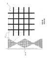
- a prior-art display and touch-screen system 300 using capacitive touch detectionincludes a display 310 with a corresponding touch screen 70 mounted with the display 310 so that information displayed on the display 310 can be viewed through the touch screen 70 .
- Graphic elements displayed on the display 310are selected, indicated, or manipulated by touching a corresponding location on the touch screen 70 .
- the touch screen 70includes a first transparent substrate 322 with first transparent electrodes 330 formed in the x-dimension on the first transparent substrate 322 and a second transparent substrate 326 with second transparent electrodes 332 formed in the y-dimension on the second transparent substrate 326 facing the x-dimension first transparent electrodes 330 .
- a dielectric layer 324is located between the first and second transparent substrates 322 , 326 and first and second transparent electrodes 330 , 332 .
- the first and second pad areas 328 , 329are separated into different parallel planes by the dielectric layer 324 .
- the first and second transparent electrodes 330 , 332have a variable width and extend in orthogonal directions (for example as shown in U.S. Patent Publication Nos. 2011/0289771 and 2011/0099805).
- a voltageis applied across the first and second transparent electrodes 330 , 332 , electric fields are formed between the first pad areas 328 of the x-dimension first transparent electrodes 330 and the second pad areas 329 of the y-dimension second transparent electrodes 332 .
- a display controller 342 connected through electrical buss connections 336controls the display 310 in coordination with a touch-screen controller 340 .
- the touch-screen controller 340is connected through electrical buss connections 336 and wires 334 and controls the touch screen 70 .
- the touch-screen controller 340detects touches on the touch screen 70 by sequentially electrically energizing and testing the x-dimension first and y-dimension second transparent electrodes 330 , 332 . Changes in capacitance between the x-dimension first and y-dimension second transparent electrodes 330 , 332 can indicate a touch.
- any electrically conductive materials located in the transparent portion of the touch-screen 70either employ transparent conductive materials (for example, transparent conductive metal oxides such as indium tin oxide) or employ conductive elements that are too small to be readily resolved by the eye of a touch-screen user.
- transparent conductive metal oxidesare well known in the display-and-touch-screen industry and have a number of disadvantages, including inadequate transparency and conductivity and a tendency to crack under mechanical or environmental stress.
- touch-screens including very fine patterns of conductive elements, such as metal wires or conductive tracesare useful.
- U.S. Patent Publication No. 2011/0007011teaches a capacitive touch screen with a mesh electrode, as does U.S. Patent Publication No. 2010/0026664.
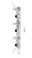
- a prior-art x- or y-dimension first or second variable-width transparent electrode 330 , 332includes a micro-pattern 356 of micro-wires 350 arranged in a rectangular grid.
- the micro-wires 350are multiple very thin metal conductive traces or wires formed on the first and second transparent substrates 322 , 326 to form the x- or y-dimension first or second transparent electrodes 330 , 332 .
- the micro-wires 350are so thin that they are not readily visible to a human observer.
- the micro-wires 350are typically opaque and spaced apart, so that the first or second transparent electrodes 330 , 332 appear to be transparent and the micro-wires 350 are not distinguished by an observer. It is important that the micro-wires 350 are accurately located in the different layers and that the different micro-wire layers are aligned to enable efficient and consistent capacitance detection resulting from electrical field disturbances when the micro-wires 350 are energized.
- Touch-screens 70 mounted over a display device 50 , 60 , 310 , as shown in FIGS. 20 , 21are largely transparent so that a user can view displayed information through the touch-screen 70 and readily locate a point on the touch-screen 70 to touch and thereby indicate information associated with the touch.
- a usercan indicate an interest, selection, or desired manipulation of the associated particular information.
- the touch-screen 70detects the touch and then electronically interacts with a computer-system processor (not shown) to indicate the touch location.
- the processorcan then associate the touch location with displayed information to execute a programmed task associated with the information. For example, graphic elements in a computer-driven graphic user interface can be selected or manipulated with a touch-screen 70 mounted on a display 310 that displays the graphic user interface.
- Capacitive touch-screensuse a variety of technologies, including resistive, inductive, capacitive, acoustic, piezoelectric, and optical technologies. Such technologies and their application in combination with displays to provide interactive control of a processor and software program are well known in the art.
- Capacitive touch-screensare of at least two different types: self-capacitive and mutual capacitive.
- Self-capacitive touch-screenscan employ an array of transparent electrodes, each of which in combination with a touching device (e.g. a finger or conductive stylus) forms a temporary capacitor whose capacitance can be detected.
- a touching devicee.g. a finger or conductive stylus
- Mutual-capacitive touch-screenscan employ an array of transparent electrode pairs that form capacitors whose capacitance is affected by a conductive touching device.
- each capacitor in the arraycan be tested to detect a touch and the physical location of the touch-detecting electrode in the touch-screen corresponds to the location of the touch.
- U.S. Pat. No. 7,663,607discloses a multipoint touch-screen having a transparent capacitive sensing medium configured to detect multiple touches or near touches that occur at the same time and at distinct locations in the plane of the touch panel and to produce distinct signals representative of the location of the touches on the plane of the touch panel for each of the multiple touches.
- the disclosureteaches both self- and mutual-capacitance touch-screens.
- Polarizersare used in the optical sciences to control light transmission and orientation.
- Liquid crystal displaysfor example, use polarizers to control the transmission or reflection of light in cooperation with electrically controllable liquid crystals.
- Organic light emitting diode (OLED) displaysare known to use circular polarizers to reduce ambient reflection from the display as taught, for example, in U.S. Patent Publication No. 2008/0129189. It is important to reduce the number of layers and elements in display systems including displays, touch-screens, and light-control layers such as polarizers in order to reduce unwanted reflection, for example of ambient light. It is also important to reduce weight and thereby enhance portability and to reduce cost of such display systems.
- a touch-responsive capacitive apparatuscomprises:
- first micro-wire layerformed on the first surface, the first micro-wire layer including a plurality of electrically connected first micro-wires;
- the second micro-wire layerformed on the second surface, the second micro-wire layer including a plurality of electrically connected second micro-wires;
- a polarizing dielectric structurelocated between the first and second micro-wire layers.
- the present inventionprovides an improved integrated apparatus and manufacturing process with reduced tolerances and costs for display devices including transparent micro-wire electrodes in a mutually capacitive touch-screen without deleteriously affecting the operation of the apparatus.
- FIG. 1is a cross section illustrating an embodiment of the present invention
- FIG. 2is a cross section illustrating another embodiment of the present invention.
- FIG. 3is a cross section illustrating an alternative embodiment of the present invention.
- FIG. 4is a cross section with a circular polarizer illustrating an alternative embodiment of the present invention.
- FIG. 5is a cross section illustrating an LCD display and touch-screen according to an embodiment of the present invention.
- FIG. 6is a cross section illustrating an OLED display and touch-screen according to an embodiment of the present invention.
- FIG. 7is a cross section illustrating an OLED display and touch-screen according to an alternative embodiment of the present invention.
- FIG. 8is a cross section illustrating an OLED display and touch-screen according to another embodiment of the present invention.
- FIG. 9is a cross section illustrating an OLED display and touch-screen and light rays according to yet another embodiment of the present invention.
- FIGS. 10A-10Care sequential cross sections illustrating a method of the present invention.
- FIGS. 11A-11Fare sequential cross sections illustrating another method of the present invention.
- FIG. 12is a flow diagram illustrating a method of the present invention.
- FIG. 13is a flow diagram illustrating another method of the present invention.
- FIG. 14is a flow diagram illustrating an alternative method of the present invention.
- FIG. 15is a flow diagram illustrating yet another method of the present invention.
- FIG. 16is a flow diagram illustrating a method of the present invention.
- FIG. 17is a flow diagram illustrating another method of the present invention.
- FIG. 18is a cross section illustrating an alternative step in a method according to an embodiment of the present invention.
- FIG. 19is a cross section of a micro-wire useful in the present invention.
- FIG. 20is cross section illustrating a display with a touch-screen according to the prior art
- FIG. 21is an exploded perspective illustrating a prior-art mutual capacitive touch screen having overlapping pad areas in conjunction with a display and controllers;
- FIG. 22is a schematic illustrating prior-art micro-wires in an apparently transparent electrode.
- a touch-responsive capacitive apparatus 5includes means for defining first and second surfaces 11 , 12 .
- a first micro-wire layer 31is formed on the first surface 11 and a second micro-wire layer 32 is formed on the second surface 12 .
- the first micro-wire layer 31includes a plurality of electrically connected first micro-wires 21 and the second micro-wire layer 32 includes a plurality of electrically connected second micro-wires 22 .
- a polarizing dielectric structure 10is located between the first and second micro-wire layers 31 , 32 .
- the micro-wire layers 31 , 32are formed on first and second surfaces 11 , 12 , respectively.
- the polarizing dielectric structure 10is a substrate, support, or layer, or can include multiple layers, supports, or substrates.
- the first and second surfaces 11 , 12are surfaces of one or more substrates, supports, or other objects having extended surface areas suitable for forming micro-wire layers.
- the substratecan have one or more layers formed thereon providing the first and second surfaces 11 , 12 with desirable surface characteristics such as mechanical stability, smoothness, impermeability, hardness, strength, resistance to environmental contaminants (e.g. liquids or gases), flexibility or rigidity, hydrophobic or hydrophilic properties, or resistance to high or low temperatures, or temperature fluctuations.
- the substratescan be transparent, for example more than 50% transparent to visible light or to light having a wavelength of 550 nm or, more preferably, more than or equal to 80% transparent to visible light or to light having a wavelength of 550 nm.
- a substrateis a polarizer, for example a linear polarizer
- the substratecan have a transparency of 30% to 50%, or more particularly from 38% to 45%.
- the first and second surfaces 11 , 12are the opposing and substantially parallel sides of the polarizing dielectric structure 10 .
- only one substrateis used.
- an alternative embodiment of a touch-responsive capacitive apparatus 5has three substrates: a first substrate 41 providing first surface 11 , a second substrate 42 providing second surface 12 , and a third substrate that is the polarizing dielectric structure 10 located between the first substrate 41 and the second substrate 42 .
- the first micro-wire layer 31is located on the first surface 11 between the first substrate 41 and the polarizing dielectric structure 10 .
- the first micro-wires 21 of the first micro-wire layer 31can be in contact with the first substrate 41 (or layers formed on the first substrate 41 ) and the polarizing dielectric structure 10 (or layers formed on the polarizing dielectric structure 10 ).
- the second micro-wire layer 32is located on the second surface 12 between the second substrate 42 and the polarizing dielectric structure 10 .
- the second micro-wires 22 of the second micro-wire layer 32can be in contact with the second substrate 42 (or layers formed on the second substrate 42 ) and the polarizing dielectric structure 10 (or layers formed on the polarizing dielectric structure 10 ). Any spaces between the first or second substrates 41 , 42 and the polarizing dielectric structure 10 that are not first or second micro-wires 21 , 22 can be filled with a transparent material 25 , for example a non-conducting polymeric material that can be index matched to other layers, for example adjacent layers such as the first or second substrates 41 , 42 or layers in the polarizing dielectric structure 10 .
- a transparent material 25for example a non-conducting polymeric material that can be index matched to other layers, for example adjacent layers such as the first or second substrates 41 , 42 or layers in the polarizing dielectric structure 10 .
- material 25is located between first substrate 41 and the polarizing dielectric layer 10 interspersed between the first micro-wires 21 .
- Material 25is also located between second substrate 42 and the polarizing dielectric layer 10 interspersed between the micro-wires 22 .
- the transparent material 25does not necessarily have an optical function but enables a solid-state structure for the touch-responsive capacitive apparatus 5 .
- the transparent material 25is omitted from the other figures but can be included according to the various embodiments of the present invention illustrated in the Figures.
- the first and second micro-wire layers 31 , 32can each include transparent material 25 and provide a solid-state layer, or not as desired.
- FIG. 3Another embodiment of a touch-responsive capacitive apparatus 5 shown in FIG. 3 has two substrates: a first substrate 41 providing first surface 11 , and a second substrate 42 (not shown) that is the polarizing dielectric structure 10 providing the second surface 12 .
- the first micro-wire layer 31is located on the first surface 11 between the first substrate 41 and the polarizing dielectric structure 10 .
- the first micro-wires 21 of the first micro-wire layer 31can be in contact with the first substrate 41 (or layers formed on the first substrate 41 ) and the polarizing dielectric structure 10 (or layers formed on the polarizing dielectric structure 10 ).
- the second micro-wires 22 of the second micro-wire layer 32are formed on the polarizing dielectric structure 10 (or layers formed on the polarizing dielectric structure 10 ) on the second surface 12 of the polarizing dielectric structure 10 opposite the first micro-wire layer 31 .
- the embodiments of FIGS. 2 and 3can also be constructed by forming either of the first or second micro-wire layers 31 , 32 on the polarizing dielectric structure 10 as shown in FIG. 1 and locating the first or second substrate 41 , 42 as shown in FIG. 2 or 3 .
- the polarizing dielectric structure 10is a linear polarizer.
- Polarizing structuresare known in the art, for example, films including poly-vinyl alcohol laminated between layers of tri-acetate cellulose film.
- either of the first or second surfaces 11 , 12is a substrate surface separate from the polarizing dielectric structure 10 (as shown in FIG. 2 ) or either of the first or second surfaces 11 , 12 is a surface of a linear polarizer or of a quarter-wave plate (not shown in FIG. 3 ) or, referring to FIG. 4 , either of the first or second surfaces 11 , 12 is a surface of a quarter-wave plate 14 .
- the quarter-wave plate 14can be a layer applied to a linear polarizer 16 as part of the polarizing dielectric structure 10 .
- Quarter-wave plates 14also known as optical retarders, are optical devices known in the prior art that alter the polarization state of light travelling through the plate.
- the polarizing dielectric substrate 10is a circular polarizer 15 .
- the second micro-wire layer 32includes second micro-wires 22 formed on the quarter-wave plate 14 opposite the linear polarizer 16 .
- Second surface 12is a surface of the quarter-wave plate 14 .
- the quarter-wave plate 14 in combination with the linear polarizer 16forms a circular polarizer 15 that serves as the polarizing dielectric structure 10 .
- First surface 11is a surface of either the linear polarizer 16 or the first substrate 41 .
- First micro-wire layer 31includes micro-wires 21 located between the linear polarizer 16 opposite the quarter-wave plate 14 and the first substrate 41 .
- first micro-wires 21 or second micro-wires 22are a metal, a metal alloy, carbon, or a material including cured or sintered metal particles, for example nickel, tungsten, silver, gold, aluminum, copper, nickel, titanium, or tin, or combinations thereof. Conductive materials are preferred.
- the first or second micro-wires 21 , 22absorb light, such as ambient light or light emitted from a device such as a display device.
- the first or second micro-wires 21 , 22are composed of a light-absorbing material, such as some forms of silver, aluminum, or carbon.
- a light-absorbing materialsuch as some forms of silver, aluminum, or carbon.
- the first or second micro-wires 21 , 22can include multiple elements, a conductive material 23 such as a metal (e.g. silver, aluminum, gold, or copper) and a light-absorbing layer 24 located over, under, or around the conductive material 23 .
- a conductive material 23such as a metal (e.g. silver, aluminum, gold, or copper)
- a light-absorbing layer 24located over, under, or around the conductive material 23 .
- Suitable light-absorbing materials for the light-absorbing layer 24can include carbon black, oxidized metals, or pigments.
- the light-absorbing layer 24can be a metal coating or layer, or a plastic or resin that includes dyes or pigments.
- the first and second micro-wires 21 , 22are too small to be readily seen by the unaided eye of a human observer.
- the first micro-wires 21 or the second micro-wires 22each have a width in a range of 0.5 um to 20 um and occupy an area less than 15% of the area of the first micro-wire layer 31 or the second micro-wire layer 32 , respectively.
- the first micro-wires 21 in the first micro-wire layer 31are electrically connected, for example in a first grid, forming a single first electrical conductor.
- the second micro-wires 22 in the second micro-wire layer 32are electrically connected, for example in a second grid, forming a single second electrical conductor.
- the first and second electrical conductorsare not electrically connected.
- the first and second gridscan be aligned, so that if viewed orthogonally to the first or second surfaces 11 , 12 , only one grid is perceived.
- the first and second gridscan be offset, so that if viewed orthogonally to the first or second surfaces 11 , 12 , two overlapping grids are perceived.
- FIG. 5illustrates the addition of a liquid-crystal display 50 to the structure illustrated in FIG. 3 .
- the liquid-crystal display 50includes a backlight 53 for emitting spatially uniform light L E over at least a portion of the extent of the display 50 , for example including lighting elements such as light-emitting diodes and light-diffusive and light-collimating layers. Such backlights are known in the display arts.
- a polarizer layer 52polarizes the backlight-emitted light L E .
- a liquid crystal layer 51that locally rotates the polarization of the light at each pixel location in response to display controller signals (e.g. display controller 342 in FIG. 21 , not shown in FIG. 5 ) providing an electric field formed by electrodes controlled by electronics (e.g. thin-film transistors) in electronic and electrode layer 54 and opposing electrodes (not shown), for example on the display cover 61 B.
- display controller signalse.g. display controller 342 in FIG. 21 , not shown in FIG. 5
- electronicse.g. thin-film transistors
- opposing electrodesnot shown
- a second linear display polarizing layer 16is the polarizing dielectric structure 10 and is arranged so that the polarization direction of layer 52 is orthogonal to the polarization direction of the polarizing dielectric structure 10 .
- Emitted light L E that is not rotated by the liquid crystal layer 51will be absorbed by the polarizing dielectric structure 10 .
- Emitted light L E that is rotated by the liquid crystal layer 51will pass through the polarizing dielectric structure 10 .
- the variation in emitted light L E across the extent of the display caused by the display controllerprovides the display information, for example graphics, text, or images.
- the first and second micro-wire layers 31 , 32 having first and second micro-wires 21 , 22are located on the first surface 11 of first substrate 41 and the second surface 12 of cover 61 B or, in an alternative embodiment, the polarizing dielectric structure 10 .
- the first and second micro-wires 21 , 22are separated by the polarizing dielectric structure 10 to form a touch-responsive capacitive apparatus 5 .
- the first substrate 41is useful to provide a protective layer (e.g. a cover 61 A) or to form a surface on which other layers (e.g. anti-reflective layers) can be formed.
- the first and second micro-wires 21 , 22can be electrically energized by a touch-screen controller (e.g. 340 in FIG. 21 ) to form an electric field that extends through the first substrate 41 .
- a touch-screen controllere.g. 340 in FIG. 21
- a conductive objecte.g. a finger touching the first substrate 41 disturbs the electric field and the capacitance of the first and second micro-wires 21 , 22 .
- This change in capacitanceis detected by the touch-screen controller (e.g. display controller 342 in FIG. 21 , not shown in FIG. 5 ).
- polarizing dielectric structure 10By functionally integrating the polarizing dielectric structure 10 into both the liquid crystal display 50 and the touch screen 70 to form a touch-responsive display apparatus 6 according to an embodiment of the present invention, fewer layers are required with a consequent savings in system thickness, materials cost, and assembly cost.
- an organic light-emitting diode display 60is integrated with a touch-responsive capacitive apparatus 5 to provide a touch-responsive display apparatus 6 .
- the arrangement of FIG. 6corresponds to the structure shown in FIG. 4 , including a first substrate 41 with a first surface 11 on which are located first micro-wires 21 forming a first micro-wire layer 31 .
- a linear polarizer 16 and quarter-wave plate 14form circular polarizer 15 and polarizing dielectric structure 10 .
- the quarter-wave plate 14provides the second surface 12 on which are located the second micro-wires 22 of second micro-wire layer 32 .
- FIG. 7includes the same first substrate 41 with first surface 11 on which are located first micro-wires 21 forming first micro-wire layer 31 .
- the linear polarizer 16 and quarter-wave plate 14form circular polarizer 15 and dielectric structure 10 .
- the second micro-wires 22 of second micro-wire layer 32are located between the linear polarizer 16 and quarter-wave plate 14 so that either the linear polarizer 16 or the quarter-wave plate 14 can provide the second surface 12 on which are located the second micro-wires 22 .
- the organic light-emitting diode display 60can include a substrate 63 , one or more electronic and emissive layer 62 , and a cover 61 .
- the locations of the substrate 63 and the cover 61can be exchanged depending on whether the organic light-emitting diode display 60 is a top-emitting display (that emits light through the cover 61 as shown in FIG. 8 ) or a bottom emitting display (that emits light through the substrate 63 as shown in FIG. 9 ).
- the first substrate 41includes first surface 11 on which are located first micro-wires 21 forming a first micro-wire layer 31 .
- the linear polarizer 16 and quarter-wave plate 14form the circular polarizer 15 and polarizing dielectric structure 10 .
- the second micro-wires 22 of second micro-wire layer 32are located on an opposite side of the polarizing dielectric structure 10 from the first micro-wire layer 31 .
- the micro-wire layers 31 , 32are formed on the first or second substrate 41 , 42 , on the polarizing dielectric structure 10 , or on the linear polarizer 16 , quarter-wave plate 14 , or other layers on any of the structures, as desired in any preferred manufacturing process.
- the micro-wires 22are formed on the cover 61 (as shown in FIG. 8 ).
- an OLED devicetypically includes a reflective surface 64 on one of the electrodes controlling the organic diodes so that emitted light L E is reflected through one side of the OLED device (unless an OLED display emitting light from both sides or a transparent OLED display is desired). This reflection improves the brightness of the OLED display on one side but also has the effect of reflecting ambient light L A so that the relative contrast of the OLED display with respect to ambient illumination is decreased, making it more difficult for a display observer to see the display.
- ambient light L A incident on the OLED displayis first polarized by polarizing dielectric structure 10 , then rotated by quarter-wave plate 14 , reflected by reflecting layer 64 , and rotated again by quarter-wave plate 14 .
- the reflected ambient light L Ais then orthogonally polarized to the incident ambient light L A and absorbed by polarizing dielectric structure 10 .
- emitted light L Eis rotated by the quarter-wave plate 14 , polarized by the polarizing dielectric structure 10 , and emitted. Since the ambient light L A is largely absorbed and the emitted light L E is not, the contrast of the OLED display is improved.
- the first and second micro-wire layers 31 , 32 having first micro-wires 21are located on the first surface 11 of first substrate 41 (or on the polarizing dielectric structure 10 ).
- the first substrate 41is useful to provide a protective layer (e.g. a cover 61 B) or to form a surface on which other layers (e.g. anti-reflective layers) can be formed.
- Second micro-wires 22are located on the second surface 12 of linear polarizer 16 , or quarter-wave plate 14 as shown, or OLED substrate 63 and separated from the first micro-wires 21 by the polarizing dielectric structure 10 to form a touch-responsive capacitive apparatus 5 .
- the first and second micro-wires 21 , 22can be electrically energized by a touch-screen controller (e.g. 340 in FIG. 21 , not shown in FIG. 9 ) to form an electric field that extends through the first or second substrates 41 or 42 .
- a conductive objecte.g. a finger touching the first substrate 41 disturbs the electric field and the capacitance of the first and second micro-wires 21 , 22 .
- This change in capacitanceis detected by the touch-screen controller.
- Organic light-emitting diode displays and liquid crystal displaysare both known in the art, as are methods for their manufacture.
- Various methods of forming micro-wires on surfacesare known in the art, for example by forming each first and second micro-wire layer 31 , 32 separately on each of the first and second surfaces 11 , 12 using lithography or printing.
- the polarizing dielectric structure 10is used to enable an efficient manufacturing method for the first and second micro-wires 21 , 22 of the first and second micro-wires layers 31 , 32 on the first and second surfaces 11 , 12 .
- a polarizing dielectric structure 10is provided in step 100 that linearly polarizes incident light.
- First and second conductive precursor material layers 44 , 46are formed (e.g. by coating) on both the first and second sides 11 , 12 of polarizing dielectric structure 10 in step 105 .
- the first surface 11can be coated at the same time as, before, or after the second surface 12 .
- the first and second conductive precursor material layers 44 , 46are then patterned in step 110 by exposing first surface 11 to first patterned light L 1 and by exposing second surface 12 to second patterned light L 2 .
- the micro-wire pattern of the first micro-wires 21can be different, or the same as, or offset from, the micro-wire pattern of the second micro-wires 22 while the electrodes themselves can be orthogonal (for example as shown with electrodes 330 , 332 in FIG. 21 ).
- Patterned lightis provided, for example, by shining light through a pattern mask or by pattern-wise exposing with laser light.
- Both the first and the second patterned light L 1 and L 2are polarized orthogonally to the direction of the polarized dielectric layer 10 and are exposed from opposite directions with respect to the polarizing dielectric substrate 10 .
- the first patterned light L 1exposes only the first conductive precursor material layer 44 and does not pass through the polarizing dielectric substrate 10 to expose the second conductive precursor material layer 46 .
- the second patterned light L 2exposes only the second conductive precursor material layer 46 and does not pass through the polarizing dielectric substrate 10 to expose the first conductive precursor material layer 44 .
- the first and second conductive precursor material layers 44 , 46are processed in step 115 , for example by curing the exposed first and second conductive precursor material layers 44 , 46 to harden exposed or unexposed portions and form conductive first and second micro-wires (e.g. 21 , 22 ) in first and second micro-wire layers 31 , 32 on the polarizing dielectric structure 10 , and washing away the undesired portions. Either positive- or negative-acting processes can be used.
- the first and second conductive precursor material layers 44 , 46are conductive precursor materials because the materials can change their nature (in particular their electrical conductivity) after curing and subsequent to coating to form the conductive first and second micro-wires 21 , 22 .
- a variety of materialscan be employed to form the patterned layer, including resins that can be cured by cross-linking wave-length-sensitive polymeric binders and silver halide materials that are exposed to light. Silver nano-particles that can be sintered to form conductive traces can also be used. Processing can include both washing out residual uncured materials and curing or exposure steps.
- the first and second conductive precursor material layers 44 , 46can be coated at the same time or at different times. Likewise, the first and second conductive precursor material layers 44 , 46 can be exposed by first and second patterned light L 1 , L 2 , respectively, at the same time or different times. Similarly, the exposed first and second conductive precursor material layers 44 , 46 can be processed at the same or different times. These separate steps can be performed together or separately even if the first and second surfaces 11 , 12 are on the same substrate (e.g. polarizing dielectric structure 10 ) or different substrates (e.g. cover 61 , substrate 63 ).
- substratee.g. polarizing dielectric structure 10
- substratese.g. cover 61 , substrate 63
- the first and second micro-wire layers 31 , 32are carefully aligned to enable an effective and consistent detection of an efficiently produced electrical field by energized first and second micro-wires 21 , 22 . If the first and second conductive precursor material layers 44 ; 46 are exposed at different times and in different locations in a manufacturing process, it is difficult to provide tight tolerances, especially at the micron scale (or smaller) needed to render the micro-wires invisible to unaided human observers. By exposing the first and second conductive precursor material layers 44 , 46 to first and second patterned light L 1 and L 2 at the same time and in the same location, better alignment between the two patterns can be achieved.
- a polarizing dielectric structure 10is provided that linearly polarizes incident light.
- the first surface 11 of the polarizing dielectric structure 10is coated with a first conductive precursor material layer 44 in step 120 as shown in FIG. 11A .
- First patterned light L 1exposes the first conductive precursor material layer 44 on the first surface 11 of the polarizing dielectric structure 10 in step 125 as shown in FIG. 11B .
- the first patterned light L 1can be polarized but need not be, since the second conductive precursor material layer 46 is not present on the second surface 12 of the polarizing dielectric structure 10 .
- the first patterned conductive precursor material layer 44is processed in step 130 to form the first micro-wires 21 in the first micro-wire layer 31 on the first surface 11 of the polarizing dielectric structure 10 .
- the second surface 12 of the polarizing dielectric structure 10is coated with a second conductive precursor material layer 46 in step 135 . Referring to FIG.
- a blanket exposure of unpatterned light L 3is directed through the polarizing dielectric structure 10 from the side of the polarizing dielectric structure 10 having the first micro-wires 21 forming the first micro-wire layer 31 to expose the second conductive precursor material layer 46 in step 140 .
- the second conductive precursor material layer 46is thus pattern-wise exposed since the first micro-wires 21 forming the first micro-wire layer 31 prevent light passing through the polarizing dielectric structure 10 to the second conductive precursor material layer 46 .
- the second conductive precursor material layer 46forms second micro-wires 22 where it is not exposed.
- the first conductive precursor material layer 44can use either positive-acting materials (as shown) or negative-acting materials.)
- step 145referring to FIG.
- the second patterned conductive precursor material layer 46is processed in step 145 to form the second micro-wires 22 in the second micro-wire layer 32 on the second surface 12 of the polarizing dielectric structure 10 .
- Second micro-wires 22 in the non-overlapped areacan be formed using the processes described above.
- the blanket exposure of unpatterned light-is replaced with a patterned positive acting light L 2 having a polarization matching that of the polarizing dielectric structure 10 directed through the polarizing dielectric structure 10 from the side of the polarizing dielectric structure 10 having the first micro-wires 21 forming the first micro-wire layer 31 to expose the second conductive precursor material layer 46 in areas not occluded by the first micro-wires 21 in step 140 .
- the second conductive precursor material layer 46is thus pattern-wise exposed in a pattern different from the pattern used to expose the first conductive precursor material layer 44 .
- the second micro-wire layer 32can have a pattern different from the first micro-wire layer 31 .
- polarizing dielectric structure 10is provided in step 100 .
- the first and second conductive precursor material layers 44 , 46are both coated on the polarizing dielectric structure 10 before either side is exposed in steps 125 , 140 , respectively.
- Polarized and first patterned light L 1is then used to expose the first conductive precursor material layer 44 in step 125 without exposing the second conductive precursor material layer 46 by using light having orthogonal polarization as the polarizing dielectric structure 10 .
- the first conductive precursor material layer 44is then processed in step 130 .
- the second conductive precursor material layeris then exposed in step 140 and processed in step 145 as also shown in FIG. 13 and FIGS. 11E and 11F .
- the second conductive precursor material layers 46respond to different frequencies or types of light than the first conductive precursor material layer 44 .
- first conductive precursor material layer 44is exposed with a first type of light that does not affect the second conductive precursor material layer 46 .
- first conductive precursor material layer 44can be sensitive to UV light whereas second conductive precursor material layer 46 can be sensitive to both UV and red light.
- the first conductive precursor material layer 44is exposed to patterned UV light, the light is polarized orthogonally to the polarizing dielectric structure 10 . In this way UV light does not pass through and expose second conductive precursor material layer 46 .
- the second conductive precursor material layer 46can be pattern-exposed to red light from either side. If exposed through the polarizing dielectric structure 10 , at least some of the red light needs to have a polarization orientation parallel to polarizing dielectric structure 10 .
- the first and second conductive precursor material layers 44 , 46are then processed.
- first and second micro-wire layers 31 , 32are made separately on separate substrates or supports.
- a first substrate 41is first provided in step 200 .
- the first surface 11 of the first substrate 41is coated with a first conductive precursor material layer 44 in step 120 .
- the first conductive precursor material layer 44is patterned in step 125 (for example by exposing the first conductive precursor material layer 44 to patterned radiation) and processed in step 130 .
- a second substrate 42is then provided in step 210 .
- the second side 12 of the second substrate 42is coated with a second conductive precursor material layer 46 in step 135 .
- the second conductive precursor material layer 46is patterned in step 140 (for example by exposing the first conductive precursor material layer 46 to patterned radiation) and processed in step 145 .
- the first and second micro-wire layers 31 , 32 of the touch-responsive capacitive apparatus 5 of the present inventionis integrated with a display, as illustrated in FIGS. 5-9 .
- a liquid crystal display 50is provided in step 250 .
- the cover 61 of the liquid crystal display 50is also the first substrate 41 and is coated with the first conductive precursor material layer 44 on first surface 11 in step 255 , patterned in step 125 , for example with patterned radiation, and processed in step 130 to form first micro-wires 21 in first micro-wire layer 31 .
- a polarizing dielectric structure 10is provided as a linear polarizer in step 261 and located over the processed first material layer in step 266 .
- a second substrate 42(serving as a protective cover for the liquid crystal layer) is then provided in step 270 , coated with the second conductive precursor material layer 46 on second surface 12 in step 275 , patterned in step 140 , for example with patterned radiation, and processed in step 145 to form second micro-wires 22 in second micro-wire layer 32 .
- the protective coveris located over the polarizing dielectric structure 10 in step 290 to form a touch screen 70 for a touch-responsive capacitive apparatus 5 in an integrated touch-responsive display apparatus 6 .
- one or both of the first and second conductive material precursor layers 44 , 46are coated on the polarizing dielectric structure 10 , for example as described with respect to FIG. 1 , rather than on the display cover 61 or second substrate 42 .
- the first and second micro-wires 21 , 22can be formed on a substrate of the LCD display 50 or other display before the substrates are incorporated into a complete display device.
- the first and second micro-wire layers 31 , 32 of the touch-responsive capacitive apparatus 5 of the present inventionis integrated with an OLED display 60 , as illustrated in FIGS. 8 and 17 .
- An OLED display 60is provided in step 250 .
- the cover 61 of the OLED display 60is also the first substrate 41 and is coated with the first conductive precursor material layer 44 (not shown on FIG. 8 ) on first surface 11 in step 255 , patterned in step 125 , for example with patterned radiation, and processed in step 130 to form first micro-wires 21 in first micro-wire layer 31 .
- a circular polarizer including a quarter-wave plate 14 and polarizing dielectric structure 10is provided in step 260 and located over the processed first material layer in step 265 .
- a second substrate 42(serving as a protective cover) is then provided in step 270 , coated with the second conductive precursor material layer 46 (not shown on FIG. 8 ) on second surface 12 in step 275 , patterned in step 140 , for example with patterned radiation, and processed in step 145 to form second micro-wires 22 in second micro-wire layer 32 .
- the protective coveris located over the polarizing dielectric structure 10 in step 290 to form a touch screen 70 for a touch-responsive capacitive apparatus 5 in an integrated touch-responsive display apparatus 6 .
- first and second material precursor layers 44 , 46are coated on the circular polarizer 15 , for example as described with respect to FIGS. 6 and 7 , rather than on the display cover 61 or second substrate 41 .
- other layers or substratesare located between the first and second micro-wire layers 31 , 32 .
- the first micro-wire layer 31can form a first electrically conductive mesh of first micro-wires 21 .
- the second micro-wire layer 32can form a second electrically conductive mesh of second micro-wires 22 .
- the first meshcan be aligned or offset with respect to the second mesh.
- the first or second conductive precursor material layers 44 , 46can include a variety of materials.
- suitable materialsinclude spectrally sensitive materials that can be exposed to patterned radiation to form first and second micro-wires 21 , 22 .
- first or second conductive precursor materials 44 , 46can be pattern-wise deposited, for example in a liquid form by an inkjet device, and then cured to form micro-wires.
- the conductive precursor material layerincludes conductive ink, conductive particles, or metal ink.
- the exposed portions of the layerscan be cured to form the first and second micro-wires 21 , 22 (for example by exposure to patterned laser light to cross-link a curable resin) and the uncured portions removed.
- unexposed portions of the first and second micro-wire layers 31 , 32can be cured to form the first and second micro-wires 21 , 22 and the cured portions removed. Materials can be deposited using inkjet deposition equipment.
- first and second micro-wire layers 31 , 32can be used to directly pattern the first and second micro-wire layers 31 , 32 , for example including patterned inkjet deposition, flexographic printing, gravure printing, electro-photographic printing, or micro-contact printing. Other methods known in the printing art for forming micro-wires can be employed.
- the first and second conductive precursor material layers 44 , 46are silver salt layers.
- the silver saltcan be any material that is capable of providing a latent image (that is, a germ or nucleus of metal in each exposed grain of metal salt) according to a desired pattern upon photo-exposure. The latent image can then be developed into a metal image.
- the silver saltcan be a spectrally photosensitive silver salt such as a silver halide or mixture of silver halides.
- the silver halidecan be, for example, silver chloride, silver bromide, silver chlorobromide, or silver bromoiodide.
- the silver salt layerincludes one or more hydrophilic binders or colloids.
- hydrophilic binders or colloidsinclude but are not limited to hydrophilic colloids such as gelatin or gelatin derivatives, polyvinyl alcohol (PVA), polyvinylpyrrolidone (PVP), casein, and mixtures thereof.
- the binder in the silver salt layerincludes one or more hardeners designed to harden the particular binder such as gelatin.
- Particularly useful hardenersinclude, but are not limited to, non-polymeric vinyl-sulfones such as bis(vinyl-sulfonyl)methane (BVSM), bis(vinyl-sulfonyl methyl)ether (BVSME), and 1,2-bis(vinyl-sulfonyl acetoamide)ethane (BVSAE).
- BVSMbis(vinyl-sulfonyl)methane
- BVSMEbis(vinyl-sulfonyl methyl)ether
- BVSAE1,2-bis(vinyl-sulfonyl acetoamide)ethane
- One useful photosensitive silver salt compositionis a high-metal (for example, silver)/low-binder (for example, gelatin) composition, that after silver salt development, is sufficiently conductive.
- the photosensitive silver salt layerincludes an emulsion of silver halide dispersed in gelatin
- a particularly useful weight ratio of silver to gelatinis 1.5:1 or higher in the silver salt layer. In certain embodiments, a ratio between 2:1 and 3:1 in the silver salt layer is particularly useful.
- the useful silver saltis a silver halide (AgX) that is sensitized to any suitable wavelength of exposing radiation.
- Organic sensitizing dyescan be used to sensitize the silver salt to visible or IR radiation, but it can be advantageous to sensitize the silver salt in the UV portion of the electromagnetic spectrum without using sensitizing dyes.
- Processing of AgX materials to form conductive tracestypically involves at least developing exposed AgX and fixing (removing) unexposed AgX. Other steps can be employed to enhance conductivity, such as thermal treatments, electro-less plating, physical development and various conductivity enhancing baths, e.g., as described in U.S. Pat. No. 3,223,525.
- the conductive precursor materialscan be liquid (for example a conductive, curable ink) and can be blanket coated in one step and pattern-wise cured by pattern-wise exposing the blanket coating in the pad and interstitial areas.
- the first and second conductive precursor material layers 44 , 46can each include a metallic particulate material or a metallic conductive precursor material, and a photosensitive binder material.
- the conductive precursor materialis conductive after it is cured and any needed processing completed. Before patterning or before curing, the conductive precursor material is not necessarily electrically conductive. As used herein, conductive precursor material is material that is electrically conductive after any final processing is completed and the conductive precursor material is not necessarily conductive at any other point in the micro-wire formation process.
- Micro-wires of the present inventionare electrically conductive after all processing is completed.
- the micro-wirescan be in a layer, with or without a binder.
- the bindercan be electrically conductive or insulating.
- the total area occupied by the first micro-wires 21is less than 15% of the first transparent conductor area and the total area occupied by the second micro-wires 22 is less than 15% of the second transparent conductor area.
- Any of the substratescan be largely transparent, for example having greater than 80% transmittance to light at 550 nm.
- the first and second micro-wires 21 , 22can have a width greater than or equal to 0.5 um and less than or equal to 20 um.
- the first and second metallic micro-wires 21 , 22can occupy an area less than 15% of the first and second micro-wire layers 31 , 32 , respectively.
- a substrateis a polarizer, for example a linear polarizer
- the substratecan have a transparency of 30% to 50%, or more particularly from 38% to 45%.
Landscapes
- Engineering & Computer Science (AREA)
- General Engineering & Computer Science (AREA)
- Theoretical Computer Science (AREA)
- Human Computer Interaction (AREA)
- Physics & Mathematics (AREA)
- General Physics & Mathematics (AREA)
- Position Input By Displaying (AREA)
Abstract
Description
- L light
- L1 first patterned light
- L2 second patterned light
- L3 unpatterned light
- LAambient light
- LEemitted light
- 5 touch-responsive capacitive apparatus
- 6 touch-responsive display apparatus
- 10 polarizing dielectric structure
- 11 first surface
- 12 second surface
- 14 quarter-wave plate
- 15 circular polarizer
- 16 linear polarizer
- 21 first micro-wire
- 22 second micro-wire
- 23 conductive material
- 24 light-absorbing layer
- 25 transparent material
- 31 first micro-wire layer
- 32 second micro-wire layer
- 41 first substrate
- 42 second substrate
- 44 first conductive precursor material layer
- 46 second conductive precursor material layer
- 50 LCD display
- 51 liquid crystal layer
- 52 polarizer layer
- 53 backlight
- 54 electronic and electrode layer
- 60 OLED display
- 61,61A,61B cover
- 62 electronic and emissive layers
- 63 substrate
- 64 reflective surface
- 70 touch-screen
- 100 provide structure step
- 105 coat sides with material layers step
- 110 pattern material layers step
- 115 process material layers step
- 120 coat first side with first material layer step
- 125 pattern first material layer step
- 130 process first material layer step
- 135 coat second side with second material layer step
- 140 pattern second material layer step
- 145 process second material layer step
- 200 provide first substrate
- 210 provide second substrate
- 250 provide OLED display step
- 255 coat cover with first material layer step
- 260 provide circular polarizer step
- 261 provide linear polarizer step
- 265 locate circular polarizer step
- 266 locate linear polarizer step
- 270 provide protective cover step
- 275 coat protective cover with second material layer step
- 290 locate protective cover step
- 300 touch screen and display system
- 310 display
- 322 first transparent substrate
- 324 dielectric layer
- 326 second transparent substrate
- 328 first pad area
- 329 second pad area
- 330 first transparent electrode
- 332 second transparent electrode
- 334 wires
- 336 buss connections
- 340 touch screen controller
- 342 display controller
- 350 micro-wires
- 356 micro-pattern
Claims (10)
Priority Applications (1)
| Application Number | Priority Date | Filing Date | Title |
|---|---|---|---|
| US13/454,145US8937604B2 (en) | 2012-02-28 | 2012-04-24 | Touch-responsive capacitor with polarizing dielectric structure |
Applications Claiming Priority (2)
| Application Number | Priority Date | Filing Date | Title |
|---|---|---|---|
| US13/406,649US8773392B2 (en) | 2012-02-28 | 2012-02-28 | Transparent touch-responsive capacitor with variable-pattern micro-wires |
| US13/454,145US8937604B2 (en) | 2012-02-28 | 2012-04-24 | Touch-responsive capacitor with polarizing dielectric structure |
Publications (2)
| Publication Number | Publication Date |
|---|---|
| US20130278544A1 US20130278544A1 (en) | 2013-10-24 |
| US8937604B2true US8937604B2 (en) | 2015-01-20 |
Family
ID=49379645
Family Applications (1)
| Application Number | Title | Priority Date | Filing Date |
|---|---|---|---|
| US13/454,145Active2032-11-16US8937604B2 (en) | 2012-02-28 | 2012-04-24 | Touch-responsive capacitor with polarizing dielectric structure |
Country Status (1)
| Country | Link |
|---|---|
| US (1) | US8937604B2 (en) |
Families Citing this family (50)
| Publication number | Priority date | Publication date | Assignee | Title |
|---|---|---|---|---|
| US8884918B2 (en)* | 2012-02-28 | 2014-11-11 | Eastman Kodak Company | Electronic device having metallic micro-wires |
| US8773395B2 (en)* | 2012-04-24 | 2014-07-08 | Eastman Kodak Company | Touch-responsive capacitor with polarizing dielectric method |
| KR101542043B1 (en)* | 2012-06-27 | 2015-08-06 | 엘지디스플레이 주식회사 | Touch screen panel |
| WO2014156827A1 (en)* | 2013-03-27 | 2014-10-02 | 富士フイルム株式会社 | Conductive sheet, manufacturing method therefor, and touch panel |
| CN104635967B (en)* | 2013-11-12 | 2018-04-10 | 宸鸿光电科技股份有限公司 | organic light emitting diode touch display device |
| CN109062448B (en)* | 2013-11-12 | 2021-07-02 | 宸鸿光电科技股份有限公司 | Organic Light Emitting Diode Touch Display Device |
| CN104765511A (en)* | 2014-01-07 | 2015-07-08 | 原相科技股份有限公司 | Capacitive touch control display device having noise shielding function |
| EP3457263A1 (en)* | 2014-12-23 | 2019-03-20 | Cambridge Touch Technologies, Ltd. | Pressure-sensitive touch panel |
| CN104881178A (en)* | 2015-06-19 | 2015-09-02 | 京东方科技集团股份有限公司 | Touch display screen, manufacturing method and display device thereof |
| KR20170004728A (en)* | 2015-07-03 | 2017-01-11 | 삼성전자주식회사 | Display panel and display apparatus having the same |
| US10475418B2 (en) | 2015-10-26 | 2019-11-12 | Reald Spark, Llc | Intelligent privacy system, apparatus, and method thereof |
| US10282046B2 (en) | 2015-12-23 | 2019-05-07 | Cambridge Touch Technologies Ltd. | Pressure-sensitive touch panel |
| EP3458897B1 (en) | 2016-05-19 | 2025-04-02 | RealD Spark, LLC | Wide angle imaging directional backlights |
| US20210199879A1 (en) | 2017-05-08 | 2021-07-01 | Reald Spark, Llc | Optical stack for imaging directional backlights |
| CN116841075A (en) | 2017-05-08 | 2023-10-03 | 瑞尔D斯帕克有限责任公司 | Optical stack for directional display |
| US10126575B1 (en) | 2017-05-08 | 2018-11-13 | Reald Spark, Llc | Optical stack for privacy display |
| US11093088B2 (en) | 2017-08-08 | 2021-08-17 | Cambridge Touch Technologies Ltd. | Device for processing signals from a pressure-sensing touch panel |
| GB2565305A (en) | 2017-08-08 | 2019-02-13 | Cambridge Touch Tech Ltd | Device for processing signals from a pressure-sensing touch panel |
| TWI878209B (en) | 2017-09-15 | 2025-04-01 | 美商瑞爾D斯帕克有限責任公司 | Display device and a view angle control optical element for application to a display device |
| US10948648B2 (en) | 2017-09-29 | 2021-03-16 | Reald Spark, Llc | Backlights having stacked waveguide and optical components with different coefficients of friction |
| WO2019090246A1 (en) | 2017-11-06 | 2019-05-09 | Reald Spark, Llc | Privacy display apparatus |
| US10976578B2 (en) | 2018-01-25 | 2021-04-13 | Reald Spark, Llc | Reflective optical stack for privacy display |
| KR102759510B1 (en) | 2018-01-25 | 2025-02-04 | 리얼디 스파크, 엘엘씨 | Touchscreen for privacy display |
| EP3769516B1 (en) | 2018-03-22 | 2025-06-25 | RealD Spark, LLC | Optical waveguide for directional backlight |
| US11079645B2 (en) | 2018-06-29 | 2021-08-03 | Reald Spark, Llc | Stabilization for privacy display |
| WO2020018552A1 (en) | 2018-07-18 | 2020-01-23 | Reald Spark, Llc | Optical stack for switchable directional display |
| US11106103B2 (en) | 2018-10-03 | 2021-08-31 | Reald Spark, Llc | Privacy display apparatus controlled in response to environment of apparatus |
| US11092852B2 (en) | 2018-11-07 | 2021-08-17 | Reald Spark, Llc | Directional display apparatus |
| US11287677B2 (en) | 2019-01-07 | 2022-03-29 | Reald Spark, Llc | Optical stack for privacy display |
| CN109782964B (en)* | 2019-01-24 | 2024-04-16 | 京东方科技集团股份有限公司 | Touch display device and manufacturing method thereof |
| GB2580700B (en) | 2019-01-25 | 2021-06-09 | Cambridge Touch Tech Ltd | Touch panel for combined capacitive touch and force sensing |
| US11029566B2 (en) | 2019-02-12 | 2021-06-08 | Reald Spark, Llc | Diffuser for privacy display |
| GB2581495A (en) | 2019-02-19 | 2020-08-26 | Cambridge Touch Tech Ltd | Force sensing touch panel |
| TW202102883A (en) | 2019-07-02 | 2021-01-16 | 美商瑞爾D斯帕克有限責任公司 | Directional display apparatus |
| WO2021026018A1 (en) | 2019-08-02 | 2021-02-11 | Reald Spark, Llc | Optical stack for privacy display |
| US11991900B2 (en)* | 2019-09-02 | 2024-05-21 | Benq Materials Corporation | Organic light emitting diode display |
| EP4038605B1 (en) | 2019-10-02 | 2024-09-25 | RealD Spark, LLC | Privacy display apparatus |
| US11733578B2 (en) | 2019-11-13 | 2023-08-22 | ReaID Spark, LLC | Display device with uniform off-axis luminance reduction |
| CN114761844A (en) | 2019-12-10 | 2022-07-15 | 瑞尔D斯帕克有限责任公司 | Control of reflection of display device |
| WO2021126707A1 (en) | 2019-12-18 | 2021-06-24 | Reald Spark, Llc | Control of ambient light for a privacy display |
| WO2021222606A1 (en) | 2020-04-30 | 2021-11-04 | Reald Spark, Llc | Directional display apparatus |
| US11353752B2 (en) | 2020-04-30 | 2022-06-07 | Reald Spark, Llc | Directional display apparatus |
| WO2021222598A1 (en) | 2020-04-30 | 2021-11-04 | Reald Spark, Llc | Directional display apparatus |
| EP4189285A4 (en) | 2020-07-29 | 2024-07-24 | RealD Spark, LLC | REAR LIGHTING FOR A SWITCHABLE DIRECTION INDICATOR |
| EP4189447A4 (en) | 2020-07-29 | 2024-07-31 | RealD Spark, LLC | Pupillated illumination apparatus |
| US11892717B2 (en) | 2021-09-30 | 2024-02-06 | Reald Spark, Llc | Marks for privacy display |
| WO2023154217A1 (en) | 2022-02-09 | 2023-08-17 | Reald Spark, Llc | Observer-tracked privacy display |
| EP4505240A1 (en) | 2022-04-07 | 2025-02-12 | RealD Spark, LLC | Directional display apparatus |
| WO2024226506A1 (en) | 2023-04-25 | 2024-10-31 | Reald Spark, Llc | Switchable privacy display |
| WO2025030030A2 (en) | 2023-08-03 | 2025-02-06 | Reald Spark, Llc | Privacy displays |
Citations (42)
| Publication number | Priority date | Publication date | Assignee | Title |
|---|---|---|---|---|
| US3223525A (en) | 1959-07-22 | 1965-12-14 | Philips Corp | Method of manufacturing, by photographic means, external, electrically conductive noble-metal patterns on non-metallic, electrically non-conductive, macromolecular supports and products obtained by these methods |
| US5066108A (en)* | 1989-12-22 | 1991-11-19 | Hughes Aircraft Company | High throughput contrast enhancement for polarized displays |
| US5942733A (en)* | 1992-06-08 | 1999-08-24 | Synaptics, Inc. | Stylus input capacitive touchpad sensor |
| US6395863B2 (en) | 2000-02-02 | 2002-05-28 | Microtouch Systems, Inc. | Touch screen with polarizer and method of making same |
| US20020171065A1 (en)* | 2001-04-02 | 2002-11-21 | Nashua Corporation | Circuit elements having an embedded conductive trace and methods of manufacture |
| US20020186209A1 (en)* | 2001-05-24 | 2002-12-12 | Eastman Kodak Company | Touch screen for use with an OLED display |
| US6645444B2 (en) | 2001-06-29 | 2003-11-11 | Nanospin Solutions | Metal nanocrystals and synthesis thereof |
| US6707450B2 (en) | 2001-03-16 | 2004-03-16 | Atouch Co., Ltd. | Touch panel with polarizer, flat panel display with the touch panel and manufacturing method thereof |
| US20040103808A1 (en)* | 2002-08-19 | 2004-06-03 | Darren Lochun | Electrical circuits and methods of manufacture and use |
| US6812637B2 (en) | 2003-03-13 | 2004-11-02 | Eastman Kodak Company | OLED display with auxiliary electrode |
| US20060057502A1 (en) | 2004-07-23 | 2006-03-16 | Sumitomo Electric Industries, Ltd. | Method of forming a conductive wiring pattern by laser irradiation and a conductive wiring pattern |
| US20060262236A1 (en) | 2002-03-01 | 2006-11-23 | Planar Systems, Inc. | Reflection resistant touch screens |
| US20060274027A1 (en)* | 2002-06-17 | 2006-12-07 | Fuji Photo Film Co., Ltd. | Image display device |
| US20070050199A1 (en)* | 2005-05-17 | 2007-03-01 | Yoshihito Ishibashi | Management system, management method, information processing apparatus, and information processing method |
| US20080048996A1 (en)* | 2006-08-11 | 2008-02-28 | Unidym, Inc. | Touch screen devices employing nanostructure networks |
| US20080129189A1 (en) | 2006-12-01 | 2008-06-05 | Cok Ronald S | Emissive displays having improved contrast |
| US20080186288A1 (en) | 2007-02-07 | 2008-08-07 | Samsung Electronics Co., Ltd. | Liquid crystal display panel and method for manufacturing the same |
| US20080266273A1 (en)* | 2007-04-24 | 2008-10-30 | White Electronic Designs Corp. | Interactive display system |
| US20080266272A1 (en)* | 2007-04-26 | 2008-10-30 | World Properties, Inc. | Luminous touch sensor |
| US20090146945A1 (en)* | 2007-12-07 | 2009-06-11 | Samsung Electronics Co., Ltd. | Touch screen panel type liquid crystal display |
| JP3152062U (en)* | 2009-03-13 | 2009-07-16 | 宸鴻光電科技股▲分▼有限公司 | Integrated structure of capacitive touch panel and liquid crystal display panel |
| US20090219258A1 (en)* | 2008-08-01 | 2009-09-03 | 3M Innovative Properties Company | Touch screen sensor with low visibility conductors |
| US20090243993A1 (en)* | 2006-10-24 | 2009-10-01 | Panasonic Corporation | Liquid-crystal panel, liquid-crystal display device, and portable terminal |
| US20100026664A1 (en) | 2008-08-01 | 2010-02-04 | Geaghan Bernard O | Touch sensitive devices with composite electrodes |
| US7663607B2 (en) | 2004-05-06 | 2010-02-16 | Apple Inc. | Multipoint touchscreen |
| US20100110040A1 (en)* | 2008-10-30 | 2010-05-06 | Samsung Electronics Co., Ltd. | Touch controller having increased sensing sensitivity, and display driving circuit and display device and system having the touch controller |
| US20100123672A1 (en) | 2008-11-14 | 2010-05-20 | Kim Eun-Ah | Organic light emitting display device |
| US20110007011A1 (en) | 2009-07-13 | 2011-01-13 | Ocular Lcd Inc. | Capacitive touch screen with a mesh electrode |
| US20110018838A1 (en)* | 2009-07-22 | 2011-01-27 | Ritdisplay Corporation | Capacitive Type Touch Panel |
| US20110099805A1 (en) | 2009-02-23 | 2011-05-05 | E&H. Co., Ltd. | Method of Fabricating Capacitive Touch-Screen Panel |
| US20110141052A1 (en)* | 2009-12-10 | 2011-06-16 | Jeffrey Traer Bernstein | Touch pad with force sensors and actuator feedback |
| US20110169767A1 (en) | 2010-01-13 | 2011-07-14 | Paul Fredrick Luther Weindorf | Polarizer capacitive touch screen |
| US20110187677A1 (en) | 2006-06-09 | 2011-08-04 | Steve Porter Hotelling | Segmented vcom |
| US20110289771A1 (en)* | 2010-05-28 | 2011-12-01 | Fujifilm Corporation | Method for producing conductive sheet and method for producing touch panel |
| US20120182261A1 (en)* | 2011-01-19 | 2012-07-19 | Wen-Chun Wang | Touch-sensitive device and touch-sensitive display device |
| US20120313880A1 (en)* | 2008-02-28 | 2012-12-13 | 3M Innovative Properties Company | Touch screen sensor with low visibility conductors |
| US20130021289A1 (en)* | 2011-07-19 | 2013-01-24 | Wei Chen | Touch sensitive displays |
| US20130049844A1 (en)* | 2011-08-23 | 2013-02-28 | Qualcomm Mems Technologies, Inc. | Capacitive touch sensor having light shielding structures |
| US20130162561A1 (en)* | 2011-12-21 | 2013-06-27 | Samsung Electro-Mechanics Co., Ltd. | Touch module |
| US20130222328A1 (en)* | 2012-02-28 | 2013-08-29 | Ronald Steven Cok | Touch screen with dummy micro-wires |
| US20130219679A1 (en)* | 2012-02-28 | 2013-08-29 | Ronald Steven Cok | Pattern-wise defining micro-wires with different heights |
| US20130278545A1 (en)* | 2012-04-24 | 2013-10-24 | Ronald Steven Cok | Touch-responsive capacitor with polarizing dielectric method |
Family Cites Families (1)
| Publication number | Priority date | Publication date | Assignee | Title |
|---|---|---|---|---|
| JPH03152062A (en)* | 1989-11-06 | 1991-06-28 | Shibaura Eng Works Co Ltd | Winding device |
- 2012
- 2012-04-24USUS13/454,145patent/US8937604B2/enactiveActive
Patent Citations (43)
| Publication number | Priority date | Publication date | Assignee | Title |
|---|---|---|---|---|
| US3223525A (en) | 1959-07-22 | 1965-12-14 | Philips Corp | Method of manufacturing, by photographic means, external, electrically conductive noble-metal patterns on non-metallic, electrically non-conductive, macromolecular supports and products obtained by these methods |
| US5066108A (en)* | 1989-12-22 | 1991-11-19 | Hughes Aircraft Company | High throughput contrast enhancement for polarized displays |
| US5942733A (en)* | 1992-06-08 | 1999-08-24 | Synaptics, Inc. | Stylus input capacitive touchpad sensor |
| US6395863B2 (en) | 2000-02-02 | 2002-05-28 | Microtouch Systems, Inc. | Touch screen with polarizer and method of making same |
| US6707450B2 (en) | 2001-03-16 | 2004-03-16 | Atouch Co., Ltd. | Touch panel with polarizer, flat panel display with the touch panel and manufacturing method thereof |
| US20020171065A1 (en)* | 2001-04-02 | 2002-11-21 | Nashua Corporation | Circuit elements having an embedded conductive trace and methods of manufacture |
| US20040209054A1 (en)* | 2001-04-02 | 2004-10-21 | Nashua Corporation | Circuit elements having an embedded conductive trace and methods of manufacture |
| US20020186209A1 (en)* | 2001-05-24 | 2002-12-12 | Eastman Kodak Company | Touch screen for use with an OLED display |
| US6645444B2 (en) | 2001-06-29 | 2003-11-11 | Nanospin Solutions | Metal nanocrystals and synthesis thereof |
| US20060262236A1 (en) | 2002-03-01 | 2006-11-23 | Planar Systems, Inc. | Reflection resistant touch screens |
| US20060274027A1 (en)* | 2002-06-17 | 2006-12-07 | Fuji Photo Film Co., Ltd. | Image display device |
| US20040103808A1 (en)* | 2002-08-19 | 2004-06-03 | Darren Lochun | Electrical circuits and methods of manufacture and use |
| US6812637B2 (en) | 2003-03-13 | 2004-11-02 | Eastman Kodak Company | OLED display with auxiliary electrode |
| US7663607B2 (en) | 2004-05-06 | 2010-02-16 | Apple Inc. | Multipoint touchscreen |
| US20060057502A1 (en) | 2004-07-23 | 2006-03-16 | Sumitomo Electric Industries, Ltd. | Method of forming a conductive wiring pattern by laser irradiation and a conductive wiring pattern |
| US20070050199A1 (en)* | 2005-05-17 | 2007-03-01 | Yoshihito Ishibashi | Management system, management method, information processing apparatus, and information processing method |
| US20110187677A1 (en) | 2006-06-09 | 2011-08-04 | Steve Porter Hotelling | Segmented vcom |
| US20080048996A1 (en)* | 2006-08-11 | 2008-02-28 | Unidym, Inc. | Touch screen devices employing nanostructure networks |
| US20090243993A1 (en)* | 2006-10-24 | 2009-10-01 | Panasonic Corporation | Liquid-crystal panel, liquid-crystal display device, and portable terminal |
| US20080129189A1 (en) | 2006-12-01 | 2008-06-05 | Cok Ronald S | Emissive displays having improved contrast |
| US20080186288A1 (en) | 2007-02-07 | 2008-08-07 | Samsung Electronics Co., Ltd. | Liquid crystal display panel and method for manufacturing the same |
| US20080266273A1 (en)* | 2007-04-24 | 2008-10-30 | White Electronic Designs Corp. | Interactive display system |
| US20080266272A1 (en)* | 2007-04-26 | 2008-10-30 | World Properties, Inc. | Luminous touch sensor |
| US20090146945A1 (en)* | 2007-12-07 | 2009-06-11 | Samsung Electronics Co., Ltd. | Touch screen panel type liquid crystal display |
| US20120313880A1 (en)* | 2008-02-28 | 2012-12-13 | 3M Innovative Properties Company | Touch screen sensor with low visibility conductors |
| US20090219258A1 (en)* | 2008-08-01 | 2009-09-03 | 3M Innovative Properties Company | Touch screen sensor with low visibility conductors |
| US20100026664A1 (en) | 2008-08-01 | 2010-02-04 | Geaghan Bernard O | Touch sensitive devices with composite electrodes |
| US20100110040A1 (en)* | 2008-10-30 | 2010-05-06 | Samsung Electronics Co., Ltd. | Touch controller having increased sensing sensitivity, and display driving circuit and display device and system having the touch controller |
| US20100123672A1 (en) | 2008-11-14 | 2010-05-20 | Kim Eun-Ah | Organic light emitting display device |
| US20110099805A1 (en) | 2009-02-23 | 2011-05-05 | E&H. Co., Ltd. | Method of Fabricating Capacitive Touch-Screen Panel |
| JP3152062U (en)* | 2009-03-13 | 2009-07-16 | 宸鴻光電科技股▲分▼有限公司 | Integrated structure of capacitive touch panel and liquid crystal display panel |
| US20110007011A1 (en) | 2009-07-13 | 2011-01-13 | Ocular Lcd Inc. | Capacitive touch screen with a mesh electrode |
| US20110018838A1 (en)* | 2009-07-22 | 2011-01-27 | Ritdisplay Corporation | Capacitive Type Touch Panel |
| US20110141052A1 (en)* | 2009-12-10 | 2011-06-16 | Jeffrey Traer Bernstein | Touch pad with force sensors and actuator feedback |
| US20110169767A1 (en) | 2010-01-13 | 2011-07-14 | Paul Fredrick Luther Weindorf | Polarizer capacitive touch screen |
| US20110289771A1 (en)* | 2010-05-28 | 2011-12-01 | Fujifilm Corporation | Method for producing conductive sheet and method for producing touch panel |
| US20120182261A1 (en)* | 2011-01-19 | 2012-07-19 | Wen-Chun Wang | Touch-sensitive device and touch-sensitive display device |
| US20130021289A1 (en)* | 2011-07-19 | 2013-01-24 | Wei Chen | Touch sensitive displays |
| US20130049844A1 (en)* | 2011-08-23 | 2013-02-28 | Qualcomm Mems Technologies, Inc. | Capacitive touch sensor having light shielding structures |
| US20130162561A1 (en)* | 2011-12-21 | 2013-06-27 | Samsung Electro-Mechanics Co., Ltd. | Touch module |
| US20130222328A1 (en)* | 2012-02-28 | 2013-08-29 | Ronald Steven Cok | Touch screen with dummy micro-wires |
| US20130219679A1 (en)* | 2012-02-28 | 2013-08-29 | Ronald Steven Cok | Pattern-wise defining micro-wires with different heights |
| US20130278545A1 (en)* | 2012-04-24 | 2013-10-24 | Ronald Steven Cok | Touch-responsive capacitor with polarizing dielectric method |
Also Published As
| Publication number | Publication date |
|---|---|
| US20130278544A1 (en) | 2013-10-24 |
Similar Documents
| Publication | Publication Date | Title |
|---|---|---|
| US8937604B2 (en) | Touch-responsive capacitor with polarizing dielectric structure | |
| US8773395B2 (en) | Touch-responsive capacitor with polarizing dielectric method | |
| US8773392B2 (en) | Transparent touch-responsive capacitor with variable-pattern micro-wires | |
| US9134860B2 (en) | Method of making a display device | |
| US8922512B2 (en) | Display apparatus with diamond-patterned micro-wire electrode | |
| US8943682B2 (en) | Making micro-wires with different heights | |
| US8773393B2 (en) | Touch screen with dummy micro-wires | |
| US8854327B2 (en) | Display apparatus with pixel-aligned ground micro-wire | |
| US8836668B2 (en) | Transparent touch-responsive capacitor with variable-height micro-wires | |
| US9024918B2 (en) | Display apparatus with pixel-aligned electrode | |
| US8884918B2 (en) | Electronic device having metallic micro-wires | |
| US8819927B2 (en) | Method of making a transparent conductor structure | |
| US20150227242A1 (en) | Transparent touch-screen capacitor with micro-wire electrode | |
| US9158420B2 (en) | Pixel-aligned diamond-patterned micro-wire electrode | |
| US8661662B1 (en) | Making transparent touch-responsive device with micro-wire electrodes | |
| US20140041924A1 (en) | Micro-wire electrode pattern | |
| US9030438B2 (en) | Pixel-aligned micro-wire electrode device | |
| US9477352B2 (en) | Making display device with pixel-aligned micro-wire electrode | |
| US9244558B2 (en) | Pixel-aligned electrode device | |
| US9098154B2 (en) | Display apparatus with pixel-aligned micro-wire electrode | |
| US8585455B1 (en) | Making display device with pixel-aligned ground micro-wire | |
| US9092088B2 (en) | Pixel-aligned ground micro-wire device | |
| US20140354899A1 (en) | Display apparatus with pixel-obscuring micro-wires | |
| US20140354898A1 (en) | Display with pixel-obscuring micro-wires | |
| US20140352143A1 (en) | Making display apparatus with pixel-obscuring micro-wires |
Legal Events
| Date | Code | Title | Description |
|---|---|---|---|
| AS | Assignment | Owner name:EASTMAN KODAK COMPANY, NEW YORK Free format text:ASSIGNMENT OF ASSIGNORS INTEREST;ASSIGNOR:COK, RONALD STEVEN;REEL/FRAME:028094/0303 Effective date:20120423 | |
| AS | Assignment | Owner name:WILMINGTON TRUST, NATIONAL ASSOCIATION, AS AGENT, MINNESOTA Free format text:PATENT SECURITY AGREEMENT;ASSIGNORS:EASTMAN KODAK COMPANY;PAKON, INC.;REEL/FRAME:030122/0235 Effective date:20130322 Owner name:WILMINGTON TRUST, NATIONAL ASSOCIATION, AS AGENT, Free format text:PATENT SECURITY AGREEMENT;ASSIGNORS:EASTMAN KODAK COMPANY;PAKON, INC.;REEL/FRAME:030122/0235 Effective date:20130322 | |
| AS | Assignment | Owner name:JPMORGAN CHASE BANK, N.A., AS ADMINISTRATIVE, DELAWARE Free format text:INTELLECTUAL PROPERTY SECURITY AGREEMENT (FIRST LIEN);ASSIGNORS:EASTMAN KODAK COMPANY;FAR EAST DEVELOPMENT LTD.;FPC INC.;AND OTHERS;REEL/FRAME:031158/0001 Effective date:20130903 Owner name:BARCLAYS BANK PLC, AS ADMINISTRATIVE AGENT, NEW YORK Free format text:INTELLECTUAL PROPERTY SECURITY AGREEMENT (SECOND LIEN);ASSIGNORS:EASTMAN KODAK COMPANY;FAR EAST DEVELOPMENT LTD.;FPC INC.;AND OTHERS;REEL/FRAME:031159/0001 Effective date:20130903 Owner name:BARCLAYS BANK PLC, AS ADMINISTRATIVE AGENT, NEW YO Free format text:INTELLECTUAL PROPERTY SECURITY AGREEMENT (SECOND LIEN);ASSIGNORS:EASTMAN KODAK COMPANY;FAR EAST DEVELOPMENT LTD.;FPC INC.;AND OTHERS;REEL/FRAME:031159/0001 Effective date:20130903 Owner name:JPMORGAN CHASE BANK, N.A., AS ADMINISTRATIVE, DELA Free format text:INTELLECTUAL PROPERTY SECURITY AGREEMENT (FIRST LIEN);ASSIGNORS:EASTMAN KODAK COMPANY;FAR EAST DEVELOPMENT LTD.;FPC INC.;AND OTHERS;REEL/FRAME:031158/0001 Effective date:20130903 Owner name:EASTMAN KODAK COMPANY, NEW YORK Free format text:RELEASE OF SECURITY INTEREST IN PATENTS;ASSIGNORS:CITICORP NORTH AMERICA, INC., AS SENIOR DIP AGENT;WILMINGTON TRUST, NATIONAL ASSOCIATION, AS JUNIOR DIP AGENT;REEL/FRAME:031157/0451 Effective date:20130903 Owner name:PAKON, INC., NEW YORK Free format text:RELEASE OF SECURITY INTEREST IN PATENTS;ASSIGNORS:CITICORP NORTH AMERICA, INC., AS SENIOR DIP AGENT;WILMINGTON TRUST, NATIONAL ASSOCIATION, AS JUNIOR DIP AGENT;REEL/FRAME:031157/0451 Effective date:20130903 Owner name:BANK OF AMERICA N.A., AS AGENT, MASSACHUSETTS Free format text:INTELLECTUAL PROPERTY SECURITY AGREEMENT (ABL);ASSIGNORS:EASTMAN KODAK COMPANY;FAR EAST DEVELOPMENT LTD.;FPC INC.;AND OTHERS;REEL/FRAME:031162/0117 Effective date:20130903 | |
| FEPP | Fee payment procedure | Free format text:PAYOR NUMBER ASSIGNED (ORIGINAL EVENT CODE: ASPN); ENTITY STATUS OF PATENT OWNER: LARGE ENTITY | |
| STCF | Information on status: patent grant | Free format text:PATENTED CASE | |
| MAFP | Maintenance fee payment | Free format text:PAYMENT OF MAINTENANCE FEE, 4TH YEAR, LARGE ENTITY (ORIGINAL EVENT CODE: M1551) Year of fee payment:4 | |
| AS | Assignment | Owner name:EASTMAN KODAK COMPANY, NEW YORK Free format text:RELEASE BY SECURED PARTY;ASSIGNOR:JP MORGAN CHASE BANK, N.A., AS ADMINISTRATIVE AGENT;REEL/FRAME:050239/0001 Effective date:20190617 Owner name:KODAK PORTUGUESA LIMITED, NEW YORK Free format text:RELEASE BY SECURED PARTY;ASSIGNOR:JP MORGAN CHASE BANK, N.A., AS ADMINISTRATIVE AGENT;REEL/FRAME:050239/0001 Effective date:20190617 Owner name:KODAK AVIATION LEASING LLC, NEW YORK Free format text:RELEASE BY SECURED PARTY;ASSIGNOR:JP MORGAN CHASE BANK, N.A., AS ADMINISTRATIVE AGENT;REEL/FRAME:050239/0001 Effective date:20190617 Owner name:KODAK REALTY, INC., NEW YORK Free format text:RELEASE BY SECURED PARTY;ASSIGNOR:JP MORGAN CHASE BANK, N.A., AS ADMINISTRATIVE AGENT;REEL/FRAME:050239/0001 Effective date:20190617 Owner name:KODAK PHILIPPINES, LTD., NEW YORK Free format text:RELEASE BY SECURED PARTY;ASSIGNOR:JP MORGAN CHASE BANK, N.A., AS ADMINISTRATIVE AGENT;REEL/FRAME:050239/0001 Effective date:20190617 Owner name:CREO MANUFACTURING AMERICA LLC, NEW YORK Free format text:RELEASE BY SECURED PARTY;ASSIGNOR:JP MORGAN CHASE BANK, N.A., AS ADMINISTRATIVE AGENT;REEL/FRAME:050239/0001 Effective date:20190617 Owner name:KODAK (NEAR EAST), INC., NEW YORK Free format text:RELEASE BY SECURED PARTY;ASSIGNOR:JP MORGAN CHASE BANK, N.A., AS ADMINISTRATIVE AGENT;REEL/FRAME:050239/0001 Effective date:20190617 Owner name:NPEC, INC., NEW YORK Free format text:RELEASE BY SECURED PARTY;ASSIGNOR:JP MORGAN CHASE BANK, N.A., AS ADMINISTRATIVE AGENT;REEL/FRAME:050239/0001 Effective date:20190617 Owner name:PAKON, INC., NEW YORK Free format text:RELEASE BY SECURED PARTY;ASSIGNOR:JP MORGAN CHASE BANK, N.A., AS ADMINISTRATIVE AGENT;REEL/FRAME:050239/0001 Effective date:20190617 Owner name:KODAK AMERICAS, LTD., NEW YORK Free format text:RELEASE BY SECURED PARTY;ASSIGNOR:JP MORGAN CHASE BANK, N.A., AS ADMINISTRATIVE AGENT;REEL/FRAME:050239/0001 Effective date:20190617 Owner name:QUALEX, INC., NEW YORK Free format text:RELEASE BY SECURED PARTY;ASSIGNOR:JP MORGAN CHASE BANK, N.A., AS ADMINISTRATIVE AGENT;REEL/FRAME:050239/0001 Effective date:20190617 Owner name:FPC, INC., NEW YORK Free format text:RELEASE BY SECURED PARTY;ASSIGNOR:JP MORGAN CHASE BANK, N.A., AS ADMINISTRATIVE AGENT;REEL/FRAME:050239/0001 Effective date:20190617 Owner name:FAR EAST DEVELOPMENT LTD., NEW YORK Free format text:RELEASE BY SECURED PARTY;ASSIGNOR:JP MORGAN CHASE BANK, N.A., AS ADMINISTRATIVE AGENT;REEL/FRAME:050239/0001 Effective date:20190617 Owner name:KODAK IMAGING NETWORK, INC., NEW YORK Free format text:RELEASE BY SECURED PARTY;ASSIGNOR:JP MORGAN CHASE BANK, N.A., AS ADMINISTRATIVE AGENT;REEL/FRAME:050239/0001 Effective date:20190617 Owner name:LASER PACIFIC MEDIA CORPORATION, NEW YORK Free format text:RELEASE BY SECURED PARTY;ASSIGNOR:JP MORGAN CHASE BANK, N.A., AS ADMINISTRATIVE AGENT;REEL/FRAME:050239/0001 Effective date:20190617 | |
| AS | Assignment | Owner name:PFC, INC., NEW YORK Free format text:RELEASE BY SECURED PARTY;ASSIGNOR:JP MORGAN CHASE BANK, N.A., AS ADMINISTRATIVE AGENT;REEL/FRAME:049901/0001 Effective date:20190617 Owner name:LASER PACIFIC MEDIA CORPORATION, NEW YORK Free format text:RELEASE BY SECURED PARTY;ASSIGNOR:JP MORGAN CHASE BANK, N.A., AS ADMINISTRATIVE AGENT;REEL/FRAME:049901/0001 Effective date:20190617 Owner name:KODAK REALTY, INC., NEW YORK Free format text:RELEASE BY SECURED PARTY;ASSIGNOR:JP MORGAN CHASE BANK, N.A., AS ADMINISTRATIVE AGENT;REEL/FRAME:049901/0001 Effective date:20190617 Owner name:CREO MANUFACTURING AMERICA LLC, NEW YORK Free format text:RELEASE BY SECURED PARTY;ASSIGNOR:JP MORGAN CHASE BANK, N.A., AS ADMINISTRATIVE AGENT;REEL/FRAME:049901/0001 Effective date:20190617 Owner name:KODAK IMAGING NETWORK, INC., NEW YORK Free format text:RELEASE BY SECURED PARTY;ASSIGNOR:JP MORGAN CHASE BANK, N.A., AS ADMINISTRATIVE AGENT;REEL/FRAME:049901/0001 Effective date:20190617 Owner name:QUALEX, INC., NEW YORK Free format text:RELEASE BY SECURED PARTY;ASSIGNOR:JP MORGAN CHASE BANK, N.A., AS ADMINISTRATIVE AGENT;REEL/FRAME:049901/0001 Effective date:20190617 Owner name:NPEC, INC., NEW YORK Free format text:RELEASE BY SECURED PARTY;ASSIGNOR:JP MORGAN CHASE BANK, N.A., AS ADMINISTRATIVE AGENT;REEL/FRAME:049901/0001 Effective date:20190617 Owner name:KODAK PHILIPPINES, LTD., NEW YORK Free format text:RELEASE BY SECURED PARTY;ASSIGNOR:JP MORGAN CHASE BANK, N.A., AS ADMINISTRATIVE AGENT;REEL/FRAME:049901/0001 Effective date:20190617 Owner name:KODAK AVIATION LEASING LLC, NEW YORK Free format text:RELEASE BY SECURED PARTY;ASSIGNOR:JP MORGAN CHASE BANK, N.A., AS ADMINISTRATIVE AGENT;REEL/FRAME:049901/0001 Effective date:20190617 Owner name:KODAK PORTUGUESA LIMITED, NEW YORK Free format text:RELEASE BY SECURED PARTY;ASSIGNOR:JP MORGAN CHASE BANK, N.A., AS ADMINISTRATIVE AGENT;REEL/FRAME:049901/0001 Effective date:20190617 Owner name:FAR EAST DEVELOPMENT LTD., NEW YORK Free format text:RELEASE BY SECURED PARTY;ASSIGNOR:JP MORGAN CHASE BANK, N.A., AS ADMINISTRATIVE AGENT;REEL/FRAME:049901/0001 Effective date:20190617 Owner name:KODAK (NEAR EAST), INC., NEW YORK Free format text:RELEASE BY SECURED PARTY;ASSIGNOR:JP MORGAN CHASE BANK, N.A., AS ADMINISTRATIVE AGENT;REEL/FRAME:049901/0001 Effective date:20190617 Owner name:KODAK AMERICAS, LTD., NEW YORK Free format text:RELEASE BY SECURED PARTY;ASSIGNOR:JP MORGAN CHASE BANK, N.A., AS ADMINISTRATIVE AGENT;REEL/FRAME:049901/0001 Effective date:20190617 Owner name:PAKON, INC., NEW YORK Free format text:RELEASE BY SECURED PARTY;ASSIGNOR:JP MORGAN CHASE BANK, N.A., AS ADMINISTRATIVE AGENT;REEL/FRAME:049901/0001 Effective date:20190617 Owner name:EASTMAN KODAK COMPANY, NEW YORK Free format text:RELEASE BY SECURED PARTY;ASSIGNOR:JP MORGAN CHASE BANK, N.A., AS ADMINISTRATIVE AGENT;REEL/FRAME:049901/0001 Effective date:20190617 | |
| AS | Assignment | Owner name:EASTMAN KODAK COMPANY, NEW YORK Free format text:RELEASE BY SECURED PARTY;ASSIGNOR:BARCLAYS BANK PLC;REEL/FRAME:052773/0001 Effective date:20170202 Owner name:KODAK AMERICAS LTD., NEW YORK Free format text:RELEASE BY SECURED PARTY;ASSIGNOR:BARCLAYS BANK PLC;REEL/FRAME:052773/0001 Effective date:20170202 Owner name:KODAK REALTY INC., NEW YORK Free format text:RELEASE BY SECURED PARTY;ASSIGNOR:BARCLAYS BANK PLC;REEL/FRAME:052773/0001 Effective date:20170202 Owner name:QUALEX INC., NEW YORK Free format text:RELEASE BY SECURED PARTY;ASSIGNOR:BARCLAYS BANK PLC;REEL/FRAME:052773/0001 Effective date:20170202 Owner name:FAR EAST DEVELOPMENT LTD., NEW YORK Free format text:RELEASE BY SECURED PARTY;ASSIGNOR:BARCLAYS BANK PLC;REEL/FRAME:052773/0001 Effective date:20170202 Owner name:KODAK (NEAR EAST) INC., NEW YORK Free format text:RELEASE BY SECURED PARTY;ASSIGNOR:BARCLAYS BANK PLC;REEL/FRAME:052773/0001 Effective date:20170202 Owner name:FPC INC., NEW YORK Free format text:RELEASE BY SECURED PARTY;ASSIGNOR:BARCLAYS BANK PLC;REEL/FRAME:052773/0001 Effective date:20170202 Owner name:NPEC INC., NEW YORK Free format text:RELEASE BY SECURED PARTY;ASSIGNOR:BARCLAYS BANK PLC;REEL/FRAME:052773/0001 Effective date:20170202 Owner name:LASER PACIFIC MEDIA CORPORATION, NEW YORK Free format text:RELEASE BY SECURED PARTY;ASSIGNOR:BARCLAYS BANK PLC;REEL/FRAME:052773/0001 Effective date:20170202 Owner name:KODAK PHILIPPINES LTD., NEW YORK Free format text:RELEASE BY SECURED PARTY;ASSIGNOR:BARCLAYS BANK PLC;REEL/FRAME:052773/0001 Effective date:20170202 | |
| AS | Assignment | Owner name:ALTER DOMUS (US) LLC, ILLINOIS Free format text:INTELLECTUAL PROPERTY SECURITY AGREEMENT;ASSIGNOR:EASTMAN KODAK COMPANY;REEL/FRAME:056733/0681 Effective date:20210226 Owner name:ALTER DOMUS (US) LLC, ILLINOIS Free format text:INTELLECTUAL PROPERTY SECURITY AGREEMENT;ASSIGNOR:EASTMAN KODAK COMPANY;REEL/FRAME:056734/0001 Effective date:20210226 Owner name:ALTER DOMUS (US) LLC, ILLINOIS Free format text:INTELLECTUAL PROPERTY SECURITY AGREEMENT;ASSIGNOR:EASTMAN KODAK COMPANY;REEL/FRAME:056734/0233 Effective date:20210226 Owner name:BANK OF AMERICA, N.A., AS AGENT, MASSACHUSETTS Free format text:NOTICE OF SECURITY INTERESTS;ASSIGNOR:EASTMAN KODAK COMPANY;REEL/FRAME:056984/0001 Effective date:20210226 | |
| MAFP | Maintenance fee payment | Free format text:PAYMENT OF MAINTENANCE FEE, 8TH YEAR, LARGE ENTITY (ORIGINAL EVENT CODE: M1552); ENTITY STATUS OF PATENT OWNER: LARGE ENTITY Year of fee payment:8 |