US8936959B1 - Integrated rf MEMS, control systems and methods - Google Patents
Integrated rf MEMS, control systems and methodsDownload PDFInfo
- Publication number
- US8936959B1 US8936959B1US13/035,969US201113035969AUS8936959B1US 8936959 B1US8936959 B1US 8936959B1US 201113035969 AUS201113035969 AUS 201113035969AUS 8936959 B1US8936959 B1US 8936959B1
- Authority
- US
- United States
- Prior art keywords
- cmos
- mems
- layer
- surface region
- forming
- Prior art date
- Legal status (The legal status is an assumption and is not a legal conclusion. Google has not performed a legal analysis and makes no representation as to the accuracy of the status listed.)
- Active, expires
Links
- 238000000034methodMethods0.000titleclaimsdescription87
- 239000000758substrateSubstances0.000claimsabstractdescription73
- 239000004065semiconductorSubstances0.000claimsabstractdescription70
- 230000008569processEffects0.000claimsdescription38
- 239000000463materialSubstances0.000claimsdescription34
- 239000002184metalSubstances0.000claimsdescription15
- 229910052751metalInorganic materials0.000claimsdescription15
- 239000002210silicon-based materialSubstances0.000claimsdescription13
- 229910021417amorphous siliconInorganic materials0.000claimsdescription7
- RTAQQCXQSZGOHL-UHFFFAOYSA-NTitaniumChemical compound[Ti]RTAQQCXQSZGOHL-UHFFFAOYSA-N0.000claimsdescription4
- 239000011521glassSubstances0.000claimsdescription4
- 239000010936titaniumSubstances0.000claimsdescription4
- 229910052719titaniumInorganic materials0.000claimsdescription4
- 230000001413cellular effectEffects0.000claimsdescription3
- 239000011261inert gasSubstances0.000claimsdescription2
- 239000007921spraySubstances0.000claimsdescription2
- 229910052710siliconInorganic materials0.000abstractdescription9
- 239000010703siliconSubstances0.000abstractdescription9
- -1e.g.Substances0.000abstractdescription6
- 238000012986modificationMethods0.000description69
- 230000004048modificationEffects0.000description69
- 238000010586diagramMethods0.000description37
- 238000005516engineering processMethods0.000description14
- 238000013461designMethods0.000description12
- 238000005538encapsulationMethods0.000description12
- 230000002093peripheral effectEffects0.000description12
- 238000004519manufacturing processMethods0.000description11
- XUIMIQQOPSSXEZ-UHFFFAOYSA-NSiliconChemical compound[Si]XUIMIQQOPSSXEZ-UHFFFAOYSA-N0.000description8
- 238000004377microelectronicMethods0.000description8
- 230000008901benefitEffects0.000description7
- 239000003990capacitorSubstances0.000description7
- 239000007769metal materialSubstances0.000description7
- 238000004806packaging method and processMethods0.000description6
- 238000004891communicationMethods0.000description5
- 229910021421monocrystalline siliconInorganic materials0.000description5
- 229910021420polycrystalline siliconInorganic materials0.000description5
- 229910045601alloyInorganic materials0.000description4
- 239000000956alloySubstances0.000description4
- 238000005452bendingMethods0.000description4
- 230000008878couplingEffects0.000description4
- 238000010168coupling processMethods0.000description4
- 238000005859coupling reactionMethods0.000description4
- 238000010297mechanical methods and processMethods0.000description4
- 230000005226mechanical processes and functionsEffects0.000description4
- 229920000642polymerPolymers0.000description4
- 239000000126substanceSubstances0.000description4
- 239000003989dielectric materialSubstances0.000description3
- 238000006073displacement reactionMethods0.000description3
- 238000001312dry etchingMethods0.000description3
- 230000006870functionEffects0.000description3
- 238000012545processingMethods0.000description3
- 238000001039wet etchingMethods0.000description3
- 244000107946Spondias cythereaSpecies0.000description2
- 238000013459approachMethods0.000description2
- 230000015572biosynthetic processEffects0.000description2
- 239000011248coating agentSubstances0.000description2
- 238000000576coating methodMethods0.000description2
- 238000007796conventional methodMethods0.000description2
- 239000013078crystalSubstances0.000description2
- 238000011161developmentMethods0.000description2
- 238000005530etchingMethods0.000description2
- 238000000227grindingMethods0.000description2
- 238000005304joiningMethods0.000description2
- 238000012544monitoring processMethods0.000description2
- 238000007517polishing processMethods0.000description2
- 239000002861polymer materialSubstances0.000description2
- 230000004044responseEffects0.000description2
- 238000003860storageMethods0.000description2
- 239000010409thin filmSubstances0.000description2
- 238000012546transferMethods0.000description2
- 240000001436Antirrhinum majusSpecies0.000description1
- 241001440311ArmadaSpecies0.000description1
- 241000251729ElasmobranchiiSpecies0.000description1
- 241001020574Gigantactis iosSpecies0.000description1
- 101000934888Homo sapiens Succinate dehydrogenase cytochrome b560 subunit, mitochondrialProteins0.000description1
- 102100025393Succinate dehydrogenase cytochrome b560 subunit, mitochondrialHuman genes0.000description1
- 241000414697TegraSpecies0.000description1
- 238000004380ashingMethods0.000description1
- 210000004556brainAnatomy0.000description1
- 230000003247decreasing effectEffects0.000description1
- 230000005670electromagnetic radiationEffects0.000description1
- 230000007613environmental effectEffects0.000description1
- 230000003203everyday effectEffects0.000description1
- 230000001815facial effectEffects0.000description1
- 230000036541healthEffects0.000description1
- 239000012212insulatorSubstances0.000description1
- 230000003993interactionEffects0.000description1
- 238000005259measurementMethods0.000description1
- 229910001092metal group alloyInorganic materials0.000description1
- 150000002739metalsChemical class0.000description1
- 230000003287optical effectEffects0.000description1
- 238000007747platingMethods0.000description1
- 238000011160researchMethods0.000description1
- 238000012827research and developmentMethods0.000description1
- 239000010454slateSubstances0.000description1
- 238000004544sputter depositionMethods0.000description1
- 230000006641stabilisationEffects0.000description1
- 238000011105stabilizationMethods0.000description1
- 230000003746surface roughnessEffects0.000description1
- 238000012360testing methodMethods0.000description1
Images


Classifications
- B—PERFORMING OPERATIONS; TRANSPORTING
- B81—MICROSTRUCTURAL TECHNOLOGY
- B81C—PROCESSES OR APPARATUS SPECIALLY ADAPTED FOR THE MANUFACTURE OR TREATMENT OF MICROSTRUCTURAL DEVICES OR SYSTEMS
- B81C1/00—Manufacture or treatment of devices or systems in or on a substrate
- B81C1/00015—Manufacture or treatment of devices or systems in or on a substrate for manufacturing microsystems
- B81C1/00222—Integrating an electronic processing unit with a micromechanical structure
- B81C1/00238—Joining a substrate with an electronic processing unit and a substrate with a micromechanical structure
- B—PERFORMING OPERATIONS; TRANSPORTING
- B81—MICROSTRUCTURAL TECHNOLOGY
- B81C—PROCESSES OR APPARATUS SPECIALLY ADAPTED FOR THE MANUFACTURE OR TREATMENT OF MICROSTRUCTURAL DEVICES OR SYSTEMS
- B81C2203/00—Forming microstructural systems
- B81C2203/07—Integrating an electronic processing unit with a micromechanical structure
- B81C2203/0785—Transfer and j oin technology, i.e. forming the electronic processing unit and the micromechanical structure on separate substrates and joining the substrates
- B81C2203/0792—Forming interconnections between the electronic processing unit and the micromechanical structure
Definitions
- the present inventionrelates generally to integrated devices. More particularly, embodiments of the present invention provide a system and method for integrating MEMS devices with other system applications configured on at least CMOS integrated circuit devices. More specifically, the present invention provides one or more MEMS devices and related elements for radio frequency (rf) applications.
- the MEMS devicescan include at least an accelerometer, a gyroscope, a magnetic sensor, a pressure sensor, a microphone, a humidity sensor, a temperature sensor, a chemical sensor, a biosensor, an inertial sensor, and others.
- the other applicationsinclude at least a sensor application or applications, system applications, and broadband applications, among others. But it will be recognized that the invention has a much broader range of applicability.
- CMOS technologyhas become the predominant fabrication technology for integrated circuits (IC).
- MEMScontinues to rely upon conventional process technologies.
- microelectronic ICsare the “brains” of an integrated device which provides decision-making capabilities
- MEMSare the “eyes” and “arms” that provide the ability to sense and control the environment.
- RFradio frequency
- IC and MEMShave limitless applications through modular measurement devices such as accelerometers, gyroscopes, actuators, and sensors.
- accelerometers and gyroscopesare used to deploy airbags and trigger dynamic stability control functions, respectively.
- MEMS gyroscopescan also be used for image stabilization systems in video and still cameras, and automatic steering systems in airplanes and torpedoes.
- Biological MEMSBio-MEMS
- Bio-MEMSimplement biosensors and chemical sensors for Lab-On-Chip applications, which integrate one or more laboratory functions on a single millimeter-sized chip only.
- Other applicationsinclude Internet and telephone networks, security and financial applications, and health care and medical systems.
- ICs and MEMScan be used to practically engage in various type of environmental interaction.
- the present inventionprovides a system and method for integrating MEMS devices with other system applications configured on at least CMOS integrated circuit devices. More specifically, the present invention provides one or more MEMS devices and related elements for radio frequency applications.
- the MEMS devicescan include at least an accelerometer, a gyroscope, a magnetic sensor, a pressure sensor, a microphone, a humidity sensor, a temperature sensor, a chemical sensor, a biosensor, an inertial sensor, and others.
- the other applicationsinclude at least a sensor application or applications, system applications, and broadband applications, among others. But it will be recognized that the invention has a much broader range of applicability.
- the present inventionprovides a method for manufacturing an rf MEMS system.
- the systemhas a semiconductor substrate, e.g., silicon.
- the systemalso has a control module provided overlying one or more first regions of the semiconductor substrate according to a specific embodiment.
- the systemalso has a base band module provided overlying one or more second regions of the semiconductor substrate and an rf module provided overlying one or more third regions of the semiconductor substrate.
- the systemalso has one or more MEMS devices integrally coupled to at least the rf module.
- the present techniqueprovides an easy to use process that relies upon conventional technology.
- the methodprovides higher device yields in dies per wafer with the integrated approach.
- the methodprovides a process and system that are compatible with conventional process technology without substantial modifications to conventional equipment and processes.
- the inventionprovides for an improved MEMS device system and related applications for a variety of uses.
- the present inventionprovides for rf MEMS and related applications, which may be integrated on one or more CMOS device structures. Depending upon the embodiment, one or more of these benefits may be achieved.
- FIG. 1is a simplified flow diagram illustrating a method of fabricating an integrated RF MEMS and control systems device according to an embodiment of the present invention
- FIG. 2is a simplified system diagram of an integrated rf MEMS system according to an embodiment of the present invention
- FIG. 3is a simplified exploded perspective view diagram of an integrated rf MEMS and CMOS devices system according to an embodiment of the present invention
- FIG. 4is a simplified side view diagram of an integrated CMOS-MEMS system according to an embodiment of the present invention.
- FIG. 5is a simplified side view diagram of an integrated CMOS-MEMS system according to another embodiment of the present invention.
- FIG. 6is a simplified side view diagram of an integrated CMOS-MEMS system according to yet another embodiment of the present invention.
- FIG. 7is a simplified side view diagram of an integrated CMOS-MEMS system according to yet another embodiment of the present invention.
- FIG. 8is a simplified side view diagram of an integrated CMOS-MEMS system according to yet another embodiment of the present invention.
- FIG. 9is a simplified side view diagram of an integrated CMOS-MEMS system according to yet another embodiment of the present invention.
- FIG. 10is a simplified top view diagram of a component of an integrated CMOS-MEMS system according to an embodiment of the present invention.
- FIG. 11is a simplified top view diagram of a component of an integrated CMOS-MEMS system according to an embodiment of the present invention.
- FIG. 12is a simplified top view diagram of a component of an integrated CMOS-MEMS system according to an embodiment of the present invention.
- FIG. 13is a simplified block diagram of a device incorporating various embodiments of the present invention.
- the present inventionprovides a system and method for integrating MEMS devices with other system applications configured on at least CMOS integrated circuit devices. More specifically, the present invention provides one or more MEMS devices and related elements for radio frequency applications.
- the MEMS devicescan include at least an accelerometer, a gyroscope, a magnetic sensor, a pressure sensor, a microphone, a humidity sensor, a temperature sensor, a chemical sensor, a biosensor, an inertial sensor, and others.
- the other applicationsinclude at least a sensor application or applications, system applications, and broadband applications, among others. But it will be recognized that the invention has a much broader range of applicability.
- FIG. 1is a simplified flow diagram illustrating a method of fabricating an integrated RF MEMS and control systems device according to an embodiment of the present invention.
- This diagramis merely an example, which should not unduly limit the scope of the claims herein.
- One of ordinary skill in the artwould recognize many other variations, modifications, and alternatives. It is also understood that the examples and embodiments described herein are for illustrative purposes only and that various modifications or changes in light thereof will be suggested to persons skilled in the art and are to be included within the spirit and purview of this process and scope of the appended claims.
- the present methodcan be briefly outlined below.
- method 100begins at start, step 102 .
- the present methodprovides a fabrication method for forming an integrated RF MEMS and control systems device.
- Many benefitsare achieved by way of the present invention over conventional techniques.
- the present techniqueprovides an easy to use process that relies upon conventional technology.
- the methodprovides higher device yields in dies per wafer with the integrated approach.
- the methodprovides a process and system that are compatible with conventional process technology without substantial modifications to conventional equipment and processes.
- the inventionprovides for an improved integrated RF MEMS and CMOS circuit device and related methods for a variety of uses. Depending upon the embodiment, one or more of these benefits may be achieved.
- fabrication method 100involves providing a first semiconductor substrate having a first surface region, step 104 .
- a control moduleis then formed on one or more first regions of the first surface region, step 106 .
- the control modulecan be provided on a first CMOS integrated circuit (IC) device region overlying the one or more first regions of the first surface region.
- the first CMOS IC circuit device regioncan have a first CMOS surface region.
- a base band moduleis formed on one or more second regions of the first surface region, step 108 , following the formation of the control module.
- the base band modulecan be provided on a second CMOS IC device region overlying one or more second regions of the first surface region.
- the second CMOS IC device regioncan have a second CMOS surface region.
- an rf moduleis formed on one or more third regions of the first surface region, step 110 , following the formation of the base band module.
- the rf modulecan be provided on a third CMOS IC device region overlying one or more third regions of the first surface region.
- the third CMOS IC device regioncan have a third CMOS surface region.
- the control module, base band module, and rf modulecan each include one or more CMOS devices.
- a dielectric layeris formed overlying the first, second, and third CMOS surface regions, step 112 .
- the dielectric layercan have one or more patterned regions.
- a second semiconductor substrateis then joined overlying the dielectric layer, step 114 .
- the second semiconductor substrate having a second surface regioncan be joined to the first, second, and third CMOS surface region.
- this joining stepcan be accomplished by bonding the second surface region to the dielectric layer.
- the second semiconductor substrateis an SOI substrate comprising a bulk portion, overlying insulating layer, and a single crystal device layer.
- the CMOS device layercan be formed using a standing CMOS process from a semiconductor foundry.
- the thinning stepcan include a grinding process to remove a thickness of material from the semiconductor substrate to expose a ground surface region. Additionally, the thinning step can include subjecting the ground surface region to a polishing process to smooth the ground surface region to a predetermined surface roughness. Also, the thinning step can include monitoring a thickness of the second substrate during either or both the grinding process and/or the polishing process. In a specific embodiment, the monitoring includes using an interferometer process to measure an indication associated with the thickness of the second substrate. The interferometer process can use an electromagnetic radiation in an infrared wavelength range.
- the thinning processcan include selectively removing the bulk portion of the SOI substrate from the single crystal device layer while maintaining attachment to the dielectric layer.
- the thinning processincludes cleaving a portion of the second semiconductor substrate at a cleave region to remove the desired thickness from the second substrate.
- the cleave regioncan be within a vicinity of the desired thickness, the desired thickness being a remaining portion of the second substrate attached to the dielectric layer.
- one or more via structuresare formed within one or more portions of the desired thickness of the second substrate, step 118 .
- the one or more via structurescan be formed within one or more portions of the second semiconductor substrate, the one or more via structures extending from the second surface region to a vicinity of the desired thickness of the second substrate.
- the one or more via structurescan also be configured as one or more stop structures to form one or more end point regions for the thinning.
- a conformal coating of metal materialis formed within the one or more via structures, step 120 .
- one or more free standing MEMS structuresare then formed within one or more potions of the desired thickness of the second substrate.
- the one or more MEMS structurescan be configured to be supported by one or more members integrally formed on the desired thickness of the second semiconductor substrate.
- the one or more MEMS structurescan be integrally coupled to at least the rf module.
- the one or more MEMS devicescan include a switch, a varactor, an inductor, and a filter.
- the one or more MEMS devicescan include a MEMS varactor coupled to a MEMS switch, the MEMS switch being coupled to one or more MEMS filters.
- a MEMS clockcan also be operably coupled to the control module.
- the one or more MEMS devicescan be formed overlying the first, second, and third CMOS surface regions.
- the one or more MEMS devicescan also include a MEMS varactor configured for an rf frequency.
- the one or more MEMS devicesincludes a bank of MEMS filters, the bank of MEMS filters being configured to transmit one or more signals in a GSM, PCS, and DCS formats.
- a sacrificial layercan be formed overlying the one or more free standing MEMS structures.
- An enclosure layercan also be formed overlying the sacrificial layer, the enclosure layer having one or more openings to expose one or more portions of the sacrificial layer.
- the enclosure layercan include a titanium material, the titanium material being activated as a getter layer.
- the enclosure layercan be selected from a metal, a semiconductor material, an amorphous silicon material, a dielectric layer, or any combination of these materials.
- the enclosure layercan be selected from a metal, a semiconductor material, an amorphous silicon material, a dielectric layer, or any combination of these materials.
- the method 100can also include removing the sacrificial layer via an ashing process to form an open region between one or more free standing MEMS structures and the enclosure layer. This step can also include forming an encapsulating layer overlying the enclosure layer to substantially seal the one or more free standing MEMS structures to form a predetermined environment within the open region.
- the predetermined environmentincludes an inert gas at a determined pressure.
- the encapsulating layeris selected from a metal layer, a spin on glass, a spray on glass, amorphous silicon, a dielectric layer, or any combination of these materials.
- the method 100can include forming one or more bond pad openings to expose one or more bond pads coupled to the CMOS device layer.
- the integrated rf MEMS and control systems devicecan be coupled to one or more power supplies.
- the integrated rf MEMS and control systems devicecan also be provided in a cellular phone apparatus.
- the above sequence of processesprovides a fabrication method for forming an integrated rf MEMS and control systems device according to an embodiment of the present invention.
- the methoduses a combination of steps including providing a substrate, forming CMOS modules, forming a thickness of a dielectric, joining a substrate overlying the circuits, thinning the substrate, and forming one or more free standing MEMS structures.
- stepsare added, one or more steps are removed, or one or more steps are provided in a different sequence without departing from the scope of the claims herein. Further details of the present method can be found throughout the present specification and more particularly below.
- FIG. 2is a simplified diagram of an rf MEMS system according to an embodiment of the present invention.
- system 200includes CMOS devices and MEMS devices 210 - 240 .
- the CMOS devices and MEMS devicescan be operably coupled and configured on a common substrate.
- MEMS devices 210 - 240can include a varactor 210 , a switch 220 , one or more filters 230 , and a resonator 240 .
- CMOS devices and MEMS devicescan be operably coupled and configured on a common substrate.
- MEMS devices 210 - 240can include a varactor 210 , a switch 220 , one or more filters 230 , and a resonator 240 .
- FIG. 3is a simplified exploded perspective diagram of an rf MEMS system according to an embodiment of the present invention.
- system 300is an rf MEMS system.
- System 300includes a semiconductor substrate 310 , (e.g. silicon) a CMOS layer 320 , and one or more MEMS devices 350 - 354 .
- semiconductor substrate 310e.g. silicon
- CMOS layer 320e.g. silicon
- MEMS devices 350 - 354e.g.
- system 300also has a control module 332 provided overlying one or more first regions of the semiconductor substrate according to a specific embodiment.
- System 300also has a base band module 331 provided overlying one or more second regions of the semiconductor substrate and an rf module 330 provided overlying one or more third regions of the semiconductor substrate.
- System 300also has one or more MEMS devices 350 - 354 integrally coupled to at least rf module 330 .
- MEMS devices 350 - 354can be integrally coupled to at least broadband module 331 , control module 332 , or further defined regions of CMOS layer 320 .
- the CMOS layer 320can include one or more bond pads 343 and can form an interface region 340 .
- MEMS devices 350 - 354can include a varactor 350 , a filter 351 , a switch 352 , an inductor 353 , and a clock 354 . These devices 350 - 354 can be formed overlying the one or more first regions of CMOS layer 320 , the one or more second regions of CMOS layer 320 , and the one or more third regions of CMOS layer 320 . These devices 350 - 354 can be operably coupled to CMOS layer 320 through interface region 340 . Additionally, MEMS clock 354 can be operably coupled to the control module 332 , which can include one or more CMOS devices.
- MEMS clock 354can be operably coupled to broadband module 331 , rf module 330 , other MEMS devices 350 - 353 , or further defined regions of CMOS layer 320 .
- MEMS varactor 350can be configured for an rf frequency, but can be configured for other frequencies as well.
- MEMS devices 350 - 354can include a bank of MEMS filters 351 , which can be configured to transmit one or more signals in formats including but not limited to GSM, PCS, and DCS. Those skilled in the art will recognize other variations, modifications, and alternatives.
- system 300can be coupled to one or more power supplies. Furthermore, system 300 can be provided in a cellular phone apparatus or any other wireless communication device. As said before, there can be other variations, modifications, and alternatives.
- FIG. 4is a simplified side view diagram of an integrated CMOS-MEMS system according to an embodiment of the present invention.
- the system 400includes a substrate layer 410 , a semiconductor layer 420 , and an encapsulation layer 440 .
- the semiconductor layer 420covers the substrate layer 410 while also creating a surface region that forms an interface region 430 .
- the common semiconductor layer 420can be made of a silicon material or any other appropriate semiconductor.
- the semiconductor layer 420can include a CMOS layer or any other appropriate layer for implementing microelectronics.
- the semiconductor layer 420can include a CMOS layer comprised of any number of metal layers and can be provided on any type of design rule, such as a 0.18 micron design rule or less.
- the interface region 430 formed by the semiconductor layercan be integrated with any number of MEMS devices and CMOS devices; the CMOS devices can be configured from a foundry compatible process.
- the CMOS and MEMS devicescan all be configured individually in separate portions of the interface region 430 .
- One skilled in the artwould recognize other variations, modifications, and alternatives.
- the overlying encapsulation layer 440can include a chip scale packaging (CSP) layer, such as a wafer level chip scale package (WL-CSP), also known as a wafer level package (WLP). Any other CSP method may be substituted if deemed appropriate by those skilled in the art. Additionally, the CSP layer 440 can be configured to hermetically seal any number of the integrated devices on the interface region 430 . Again, there can be many other variations, modifications, and alternatives.
- CSPchip scale packaging
- WL-CSPwafer level chip scale package
- WLPwafer level package
- FIG. 5is a simplified side view diagram of an integrated CMOS-MEMS system according to another embodiment of the present invention.
- the system 500includes a substrate layer 510 , a semiconductor layer 520 , an integrated device 540 , and an encapsulation layer 550 .
- the semiconductor layer 520covers the substrate layer 510 while also creating a surface region that forms an interface region 530 .
- the common semiconductor layer 520can be made of a silicon material or any other appropriate semiconductor.
- the semiconductor layer 520can include a CMOS layer or any other appropriate layer for implementing microelectronics.
- the semiconductor layer 520can include a CMOS layer comprised of any number of metal layers and can be provided on any type of design rule, such as a 0.18 micron design rule or less.
- the interface region 530 formed by the semiconductor layercan be integrated with any number of MEMS devices and CMOS devices; the CMOS devices can be configured from a foundry compatible process. The CMOS and MEMS devices can all be configured individually in separate portions of the interface region 530 .
- One skilled in the artwould recognize other variations, modifications, and alternatives.
- the integrated device 540can be an accelerometer.
- any number of MEMS devicescan be included in the integrated system 500 , and each of these devices can comprise one or more deposited materials, one or more bonded materials, or others.
- each of these devicescan comprise one or more deposited materials, one or more bonded materials, or others.
- the overlying encapsulation layer 540can include a chip scale packaging (CSP) layer, such as a wafer level chip scale package (WL-CSP), also known as a wafer level package (WLP). Any other CSP method may be substituted if deemed appropriate by those skilled in the art. Additionally, the CSP layer 540 can be configured to hermetically seal any number of the integrated devices on the interface region 530 . Again, there can be many other variations, modifications, and alternatives.
- CSPchip scale packaging
- WL-CSPwafer level chip scale package
- WLPwafer level package
- FIG. 6is a simplified side view diagram of an integrated CMOS-MEMS system according to yet another embodiment of the present invention.
- the system 600includes a substrate layer 610 , a semiconductor layer 620 , an integrated device 640 , and an encapsulation layer 650 .
- the semiconductor layer 620covers the substrate layer 610 while also creating a surface region that forms an interface region 630 .
- the common semiconductor layer 620can be made of a silicon material or any other appropriate semiconductor.
- the semiconductor layer 620can include a CMOS layer or any other appropriate layer for implementing microelectronics.
- the semiconductor layer 620can include a CMOS layer comprised of any number of metal layers and can be provided on any type of design rule, such as a 0.18 micron design rule or less.
- the interface region 630 formed by the semiconductor layercan be integrated with any number of MEMS devices and CMOS devices; the CMOS devices can be configured from a foundry compatible process. The CMOS and MEMS devices can all be configured individually in separate portions of the interface region 630 .
- One skilled in the artwould recognize other variations, modifications, and alternatives.
- the integrated device 640can be a gyroscope.
- any number of MEMS devicescan be included in the integrated system 600 , and each of these devices can comprise one or more deposited materials, one or more bonded materials, or others.
- each of these devicescan comprise one or more deposited materials, one or more bonded materials, or others.
- the overlying encapsulation layer 640can include a chip scale packaging (CSP) layer, such as a wafer level chip scale package (WL-CSP), also known as a wafer level package (WLP). Any other CSP method may be substituted if deemed appropriate by those skilled in the art. Additionally, the CSP layer 640 can be configured to hermetically seal any number of the integrated devices on the interface region 630 . Again, there can be many other variations, modifications, and alternatives.
- CSPchip scale packaging
- WL-CSPwafer level chip scale package
- WLPwafer level package
- FIG. 7is a simplified side view diagram of an integrated CMOS-MEMS system according to yet another embodiment of the present invention.
- the system 700includes a substrate layer 710 , a semiconductor layer 720 , an integrated device 740 , and an encapsulation layer 750 .
- the semiconductor layer 720covers the substrate layer 710 while also creating a surface region that forms an interface region 730 .
- the common semiconductor layer 720can be made of a silicon material or any other appropriate semiconductor.
- the semiconductor layer 720can include a CMOS layer or any other appropriate layer for implementing microelectronics.
- the semiconductor layer 720can include a CMOS layer comprised of any number of metal layers and can be provided on any type of design rule, such as a 0.18 micron design rule or less.
- the interface region 730 formed by the semiconductor layercan be integrated with any number of MEMS devices and CMOS devices; the CMOS devices can be configured from a foundry compatible process.
- the CMOS and MEMS devicescan all be configured individually in separate portions of the interface region 730 .
- One skilled in the artwould recognize other variations, modifications, and alternatives.
- the integrated device 740can be a magnetic sensor.
- any number of MEMS devicescan be included in the integrated system 700 , and each of these devices can comprise one or more deposited materials, one or more bonded materials, or others.
- each of these devicescan comprise one or more deposited materials, one or more bonded materials, or others.
- the overlying encapsulation layer 740can include a chip scale packaging (CSP) layer, such as a wafer level chip scale package (WL-CSP), also known as a wafer level package (WLP). Any other CSP method may be substituted if deemed appropriate by those skilled in the art. Additionally, the CSP layer 740 can be configured to hermetically seal any number of the integrated devices on the interface region 730 . Again, there can be many other variations, modifications, and alternatives.
- CSPchip scale packaging
- WL-CSPwafer level chip scale package
- WLPwafer level package
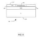
- FIG. 8is a simplified side view diagram of an integrated CMOS-MEMS system according to yet another embodiment of the present invention.
- the system 800includes a substrate layer 810 , a semiconductor layer 820 , an integrated device 840 , and an encapsulation layer 850 .
- the semiconductor layer 820covers the substrate layer 810 while also creating a surface region that forms an interface region 830 .
- the common semiconductor layer 820can be made of a silicon material or any other appropriate semiconductor.
- the semiconductor layer 820can include a CMOS layer or any other appropriate layer for implementing microelectronics.
- the semiconductor layer 820can include a CMOS layer comprised of any number of metal layers and can be provided on any type of design rule, such as a 0.18 micron design rule or less.
- the interface region 830 formed by the semiconductor layercan be integrated with any number of MEMS devices and CMOS devices; the CMOS devices can be configured from a foundry compatible process.
- the CMOS and MEMS devicescan all be configured individually in separate portions of the interface region 830 .
- One skilled in the artwould recognize other variations, modifications, and alternatives.
- the integrated device 840can be a pressure sensor.
- any number of MEMS devicescan be included in the integrated system 800 , and each of these devices can comprise one or more deposited materials, one or more bonded materials, or others.
- each of these devicescan comprise one or more deposited materials, one or more bonded materials, or others.
- the overlying encapsulation layer 840can include a chip scale packaging (CSP) layer, such as a wafer level chip scale package (WL-CSP), also known as a wafer level package (WLP). Any other CSP method may be substituted if deemed appropriate by those skilled in the art. Additionally, the CSP layer 840 can be configured to hermetically seal any number of the integrated devices on the interface region 830 . Again, there can be many other variations, modifications, and alternatives.
- CSPchip scale packaging
- WL-CSPwafer level chip scale package
- WLPwafer level package
- FIG. 9is a simplified side view diagram of an integrated CMOS-MEMS system according to yet another embodiment of the present invention.
- the system 900includes a substrate layer 910 , a semiconductor layer 920 , a CMOS device 940 , and an encapsulation layer 950 .
- the semiconductor layer 920covers the substrate layer 910 while also creating a surface region that forms an interface region 930 .
- the common semiconductor layer 920can be made of a silicon material or any other appropriate semiconductor.
- the semiconductor layer 920can include a CMOS layer or any other appropriate layer for implementing microelectronics.
- the semiconductor layer 920can include a CMOS layer comprised of any number of metal layers and can be provided on any type of design rule, such as a 0.18 micron design rule or less.
- the CMOS device 940can be integrated into the CMOS layer 920 and configured with the interface region 930 . Also, the CMOS device 940 can be configured from a foundry compatible process. Also, the interface region 930 formed by the semiconductor layer can be integrated with any number of MEMS devices and CMOS devices; the CMOS devices can be configured from a foundry compatible process. In various embodiments, any number of MEMS devices may be fabricated substantially simultaneously upon interface region 930 .
- MEMS devicesmay or may not be patterned using the same masks as other MEMS devices, MEMS devices may or may not be fabricated using deposited material that is used for other MEMS devices, MEMS devices may or may not be fabricated using the same process steps that are used to fabricate other MEMS devices, or the like.
- MEMS devicesmay or may not be fabricated using the same process steps that are used to fabricate other MEMS devices, or the like.
- FIGS. 10-12illustrate an example of some of the MEMS devices that can be fabricated approximately in parallel using the techniques described above.
- the CMOS and MEMS devicescan all be configured individually in separate portions of the interface region 930 .
- One skilled in the artwould recognize other variations, modifications, and alternatives.
- the overlying encapsulation layer 950can include a chip scale packaging (CSP) layer, such as a wafer level chip scale package (WL-CSP), also known as a wafer level package (WLP). Any other CSP method may be substituted if deemed appropriate by those skilled in the art. Additionally, the CSP layer 950 can be configured to hermetically seal any number of the integrated devices on the interface region 930 . Again, there can be many other variations, modifications, and alternatives.
- CSPchip scale packaging
- WL-CSPwafer level chip scale package
- WLPwafer level package
- FIG. 10is a simplified top view diagram of a component of an integrated MEMS-CMOS system according to an embodiment of the present invention. More particularly, the component can be a transducer apparatus, which can be a component of an inertial sensing device, such as an accelerometer. As shown, apparatus 1000 includes a movable base structure 1010 , at least one intermediate anchor structure 1020 , and at least one intermediate spring structure 1030 . In an embodiment, apparatus 1000 can be configured to improve tolerance of external deformations. Those of ordinary skill in the art will recognize other variations, modifications, and alternatives.
- movable base structure 1010can have an outer surface region, and have at least one portion removed to form at least one inner surface region 1002 .
- movable base structure 1010can be formed from a single crystal silicon, polycrystalline silicon, or amorphous silicon material.
- Moveable base structure 1010can also include a thickness of a polymer or a thickness of a metal material.
- movable base structure 1010can include other materials and combinations thereof.
- movable base structure 1010can be a rectangular movable base structure, a patterned polygonal base structure, or the like.
- intermediate anchor structure(s) 1020can be spatially disposed within a vicinity of inner surface region(s) 1002 of the movable base structure.
- intermediate anchor structure(s) 1020can be formed from single crystal silicon, polycrystalline silicon, amorphous silicon material, or the like.
- Intermediate anchor structure(s) 1020can also include a polymer or metal material, or other materials or combinations thereof.
- intermediate spring structure(s) 1030can be operably coupled to the intermediate anchor structure(s) 1020 and at least one portion of inner surface region(s) 1002 of movable base structure 1010 .
- intermediate spring structure(s) 1030can be formed from single crystal silicon, polycrystalline silicon, amorphous silicon material, or the like.
- Intermediate spring structure(s) 1030can also include a polymer or metal material, or other materials or combinations thereof.
- intermediate spring structure(s) 1030can be spatially oriented to be substantially 45 degrees or substantially (pi/4) radians to the edges of the die.
- the intermediate spring structure(s)can have at least one segment having a segment length.
- the segments of the springwhich are connected by folds, are used as a reference.
- the segmentswould be positioned such that the segments are perpendicular to diagonal lines 1001 .
- Another way to determine the orientation of a springcan be done by drawing a “line” connecting the contacts of the spring from the anchor to the movable base (i.e. the end points of the spring). In this case, the proper orientation of the spring would have the “line” forming a substantially 45 degree or (pi/4) radian angle with the edges of a die (pointed along diagonal lines 1001 ).
- apparatus 1000can include at least one capacitor element spatially disposed within a vicinity of inner surface region(s) 1002 of movable base structure 1010 .
- the capacitor element(s)can include a fixed capacitor element and a movable capacitor element.
- the movable capacitor elementwill generally be disposed in a portion of the movable base structure 1010 .
- the physical basis of apparatus 1000is to have the average displacement of the fixed capacitor element(s) match the average displacement of the movable capacitor element(s) in response to external deformations.
- apparatus 1000can be coupled to another MEMS device or an electronic device.
- apparatus 1000can be configured to be tolerant of external deformations.
- Apparatus 1000can be a transducer apparatus which reduces the area needed for anchors and springs and provides more area for other MEMS components. There can be other variations, modifications, and alternatives as well. Further embodiments of the above device may be found in the co-pending patent application, referred to above.
- FIG. 10is a simplified top view diagram of a component of an integrated MEMS-CMOS system according to various embodiments of the present invention. More particularly, the component can be an inertial sensing device, such as a gyroscope.
- device 1100which can be disposed upon a substrate having a surface region, includes at least one anchor structure 1110 , at least one frame structure 1120 , at least one movable structure, at least one first flexible member, and at least one second flexible member.
- the movable structure(s)can include at least one peripheral movable structure 1130 and at least one central movable structure 1140 .
- the first flexible member(s)can include flexible anchor member(s) 1150 and the second flexible member(s) can include at least one flexible frame member 1160 and/or at least one flexible structure member 1170 .
- the second flexible member(s)can include at least one flexible frame member 1160 and/or at least one flexible structure member 1170 .
- the substratecan include a buried oxide (BOX) substrate.
- the substratecan include an epitaxial (EPI) material.
- the substratecan have a silicon, single crystal silicon, or polycrystalline silicon material.
- the substratecan also include a dielectric material, a metal material, a metal alloy, or other materials or combination of materials thereof.
- the substratecan have an integrated circuit layer, such as a CMOS device layer, formed overlying the substrate.
- the substrateincludes a surface region. At least one anchor structure 1110 can be formed overlying the surface region. At least one flexible anchor member 1150 is coupled to at least a portion of the anchor structure(s).
- anchor structure(s) 1110 and flexible anchor member(s) 1150can include a silicon, dielectric, metal, alloy, or other materials or combination thereof.
- flexible anchor members 1150can include torsion spring(s) or bending spring(s).
- anchor structure(s) 1110 and flexible anchor member(s) 1150can be formed together during the same fabrication processes or separately by performing a wet or dry etching or mechanical process. Of course, there can be other variations, modifications, and alternatives.
- frame structure(s) 1120can be formed having at least a portion coupled to flexible anchor member(s) 1150 .
- Flexible frame member(s) 1160can be formed and coupled to at least a portion of frame structure(s) 1120 .
- at least one flexible coupling member 1180can be formed to couple frame structure(s) 1120 .
- frame structure(s) 1120 , flexible coupling member(s) 1180 and flexible frame member(s) 1160can include a silicon, dielectric, metal, alloy, or other materials or combinations thereof.
- flexible frame member(s) 1160 and flexible coupling member(s) 1180can include torsion spring(s) or bending spring(s).
- frame structure(s) 1120 , flexible coupling member(s) 1180 , and flexible frame member(s) 1160can be formed together during the same fabrication processes or separately by performing a wet or dry etching or mechanical process. As stated previously, there can be other variations, modifications, and alternatives.
- peripheral movable structure(s) 1130can be formed overlying the substrate, having at least one portion coupled to flexible frame member(s) 1160 .
- the movable structure(s), which can be peripheral movable structure(s) 1130can have at least one flexible tilting member.
- Flexible structure member(s) 1170can be formed and coupled to at least a portion of peripheral movable structure(s) 1130 .
- flexible structure member(s) 1170can be coupled to central movable structure(s) 1140 , which can be formed overlying the substrate.
- peripheral movable structure 1130 , central movable structure 1140 , flexible structure and tilting member(s)can include a silicon, dielectric, metal, alloy, or other materials or combinations thereof.
- the flexible structure and tilting member(s)can include torsion spring(s) or bending spring(s).
- Other torsion springs or bending springscan also be formed within at least one portion of central movable structure(s) 1140 , such as the underside of central movable structure(s) 1140 which overlies the substrate.
- the movable structurescan be formed within frame structure(s) 1120 .
- four peripheral movable structures 1130 and two central movable structures 1140are shown formed within two frame structures 1120 .
- Each frame structures 1120are coupled to two peripheral movable structures 1130 and one central movable structure 1140 .
- the peripheral and central movable structures 1130 / 1140can be proof masses, which can be predetermined test masses used in a measuring device.
- the peripheral and central movable structure(s) 1130 / 1140 and the flexible structure and tilting member(s) [referring to flexible structure member(s) 1170 ]can be formed together or separately by performing a wet or dry etching or mechanical process. Again, there can be other variations, modifications, and alternatives.
- At least one comb structure 1190can be formed and coupled to at least one portion of frame structure(s) 1120 .
- comb structure(s) 1190can be anti-phase driving comb structure(s), which can include a silicon, dielectric, metal, alloy, or other materials or combinations thereof.
- the peripheral and central movable structure(s) 1130 / 1140can have stop structures 1101 , which can be used to set the boundaries of any vibration, movement, or displacement. A portion of peripheral movable structure 1130 and central movable structure 1140 may be removed.
- peripheral movable structure 1130 and central movable structure 1140perforations within a line or an array of perforations.
- the perforationscan be formed by performing an etching process or mechanical process.
- all elements mentioned previouscan be formed by performing an etching process on one wafer or material.
- there can be other variations, modifications, and alternatives. Further embodiments of the above deviceare disclosed in the co-pending patent application referred to above.
- FIG. 12is a simplified top view diagram of a component of an integrated MEMS-CMOS system according to an embodiment of the present invention.
- This diagramwhich can represent a partially formed three-axis magnetic field sensor device or a two-axis magnetic field sensor device, is merely an example, which should not unduly limit the scope of the claims herein.
- device 1200includes a substrate 1210 , an integrated circuit (IC) layer 1220 , a first magnetic field sensor element 1230 , and a second magnetic field sensor element 1240 .
- ICintegrated circuit
- substrate 1210can have a surface region.
- substrate 1210can include a buried oxide (BOX) substrate.
- substrate 1210can include a substrate-on-insulator (SOI) substrate.
- substrate 1210can include an epitaxial (EPI) material.
- substrate 1210can have a silicon, single crystal silicon, or polycrystalline silicon material.
- substrate 1210can also include metals, dielectrics, polymers, and other materials and combinations thereof. Those skilled in the art will recognize other variations, modifications, and alternatives.
- IC layer 1220can be formed overlying at least one portion of the surface region.
- IC layer 1220can include an application specific integrated circuit (ASIC) layer, or other type of IC layer or combination thereof.
- ASICapplication specific integrated circuit
- IC layer 1220can include at least one IC device, CMOS device, or other device.
- IC layer 1220can be coupled to the first and second magnetic field sensor elements 1230 and 1240 .
- first magnetic field sensor element(s) 1230 and second magnetic field sensor element 1240can be formed overlying at least one portion of the surface region.
- Magnetic field sensor elements 1230 and 1240can include ordinary magneto-resistive (OMR) device(s), anisotropic magneto-resistive (AMR) device(s), giant magneto-resistive (GMR) device(s), or tunnel junction magneto-resistive (TMR) device(s).
- Elements 1230 and 1240can also be other types of magnetic field sensor devices, sensors, or combinations thereof.
- magnetic field sensor elements 1230 and 1240can include thin film devices that can be deposited overlying at least one portion of the surface region.
- the thin film device(s)can be deposited by a sputtering process or an electric plating process.
- magnetic field sensor elements 1230 and 1240are formed as a Wheatstone bridge, a half bridge, or a single element configuration.
- magnetic field sensor elements 1230 and 1240can include at least one layer of dielectric material and/or metal material. As stated previously, there can be other variations, modifications, and alternatives. Further embodiments of the above device are disclosed in the co-pending patent application referred to above.
- FIG. 13illustrates a functional block diagram of various embodiments of the present invention.
- a computing device 1300typically includes an applications processor 1310 , memory 1320 , a touch screen display 1330 and driver 1340 , an image acquisition device 1350 , audio input/output devices 1360 , and the like. Additional communications from and to computing device are typically provided by via a wired interface 1370 , a GPS/Wi-Fi/Bluetooth interface 1380 , RF interfaces 1390 and driver 1400 , and the like. Also included in various embodiments are physical sensors 1410 .
- computing device 1300may be a hand-held computing device (e.g. Apple iPad, Apple iTouch, Dell Mini slate/Streak, Lenovo Skylight/IdeaPad, Samsung Galaxy Tab, Asus EEE series, HP Slate, Notion Ink Adam), a portable telephone (e.g. Apple iPhone, Motorola Droid, Google Nexus One, HTC Incredible/EVO 4G, Palm Pre series, Nokia N900), a portable computer (e.g. netbook, laptop), a media player (e.g. Microsoft Zune, Apple iPod), a reading device (e.g. Amazon Kindle, Barnes and Noble Nook), or the like.
- a hand-held computing devicee.g. Apple iPad, Apple iTouch, Dell Mini slate/Streak, Lenovo Skylight/IdeaPad, Samsung Galaxy Tab, Asus EEE series, HP Slate, Notion Ink Adam
- a portable telephonee.g. Apple iPhone, Motorola Droid, Google Nexus One, HTC Incredible/EVO 4G, Palm Pre series, Nokia N900
- computing device 1300may include one or more processors 1310 .
- processors 1310may also be termed application processors, and may include a processor core, a video/graphics core, and other cores.
- Processors 1310may be a processor from Apple (A4), Intel (Atom), NVidia (Tegra 2), Marvell (Armada), Qualcomm (Snapdragon), Samsung, TI (OMAP), or the like.
- the processor coremay be an Intel processor, an ARM Holdings processor such as the Cortex-A, -M, -R or ARM series processors, or the like.
- the video/graphics coremay be an Imagination Technologies processor PowerVR-SGX, -MBX, -VGX graphics, an Nvidia graphics processor (e.g. GeForce), or the like.
- Other processing capabilitymay include audio processors, interface controllers, and the like. It is contemplated that other existing and/or later-developed processors may be used in various embodiments of the present invention.
- memory 1320may include different types of memory (including memory controllers), such as flash memory (e.g. NOR, NAND), pseudo SRAM, DDR SDRAM, or the like.
- Memory 1320may be fixed within computing device 1300 or removable (e.g. SD, SDHC, MMC, MINI SD, MICRO SD, CF, SIM).
- computer-executable software codee.g. firmware, application programs
- application dataoperating system data or the like. It is contemplated that other existing and/or later-developed memory and memory technology may be used in various embodiments of the present invention.
- touch screen display 1330 and driver 1340may be based upon a variety of later-developed or current touch screen technology including resistive displays, capacitive displays, optical sensor displays, electromagnetic resonance, or the like. Additionally, touch screen display 1330 may include single touch or multiple-touch sensing capability. Any later-developed or conventional output display technology may be used for the output display, such as TFT-LCD, OLED, Plasma, trans-reflective (Pixel Qi), electronic ink (e.g. electrophoretic, electrowetting, interferometric modulating). In various embodiments, the resolution of such displays and the resolution of such touch sensors may be set based upon engineering or non-engineering factors (e.g. sales, marketing). In some embodiments of the present invention, a display output port, such as an HDMI-based port or DVI-based port may also be included.
- a display output portsuch as an HDMI-based port or DVI-based port may also be included.
- image capture device 1350may include a sensor, driver, lens and the like.
- the sensormay be based upon any later-developed or convention sensor technology, such as CMOS, CCD, or the like.
- image recognition software programsare provided to process the image data.
- such softwaremay provide functionality such as: facial recognition, head tracking, camera parameter control, or the like.
- audio input/output 1360may include conventional microphone(s)/speakers. In some embodiments of the present invention, three-wire or four-wire audio connector ports are included to enable the user to use an external audio device such as external speakers, headphones or combination headphone/microphones.
- voice processing and/or recognition softwaremay be provided to applications processor 1310 to enable the user to operate computing device 1300 by stating voice commands. Additionally, a speech engine may be provided in various embodiments to enable computing device 1300 to provide audio status messages, audio response messages, or the like.
- wired interface 1370may be used to provide data transfers between computing device 1300 and an external source, such as a computer, a remote server, a storage network, another computing device 1300 , or the like.
- datamay include application data, operating system data, firmware, or the like.
- Embodimentsmay include any later-developed or conventional physical interface/protocol, such as: USB 2.0, 3.0, micro USB, mini USB, Firewire, Apple iPod connector, Ethernet, POTS, or the like. Additionally, software that enables communications over such networks is typically provided.
- a wireless interface 1380may also be provided to provide wireless data transfers between computing device 1300 and external sources, such as computers, storage networks, headphones, microphones, cameras, or the like.
- wireless protocolsmay include Wi-Fi (e.g. IEEE 802.11a/b/g/n, WiMax), Bluetooth, IR and the like.
- GPS receiving capabilitymay also be included in various embodiments of the present invention, however is not required. As illustrated in FIG. 13 , GPS functionality is included as part of wireless interface 1380 merely for sake of convenience, although in implementation, such functionality is currently performed by circuitry that is distinct from the Wi-Fi circuitry and distinct from the Bluetooth circuitry.
- RF interfaces 1390may support any future-developed or conventional radio frequency communications protocol, such as CDMA-based protocols (e.g. WCDMA), GSM-based protocols, HSUPA-based protocols, or the like.
- CDMA-based protocolse.g. WCDMA
- GSM-based protocolse.g. GSM-based protocols
- HSUPA-based protocolse.g. HSUPA-based protocols
- driver 1400is illustrated as being distinct from applications processor 1310 . However, in some embodiments, these functionality are provided upon a single IC package, for example the Marvel PXA330 processor, and the like. It is contemplated that some embodiments of computing device 1300 need not include the RF functionality provided by RF interface 1390 and driver 1400 .
- FIG. 13also illustrates computing device 1300 to include physical sensors 1410 .
- physical sensors 1410can be single axis or multi-axis Micro-Electro-Mechanical Systems (MEMS) based devices being developed by M-cube, the assignee of the present patent application.
- Physical sensors 1410can include accelerometers, gyroscopes, pressure sensors, magnetic field sensors, bio sensors, and the like.
- physical sensors 1410may fabricated using the combined CMOS MEMS fabrication techniques described above. More specifically, one or more MEMS devices may be fabricated approximately in parallel using common masks, layers, and processes, above a substrate. In various embodiments, the substrate may be on top of a CMOS device. Both the CMOS and MEMS device may be fabricated using foundry-compatible processes.
- conventional physical sensors 1410from Bosch, STMicroelectronics, Analog Devices, Kionix or the like may be used.
- any number of future developed or current operating systemsmay be supported, such as iPhone OS (e.g. iOS), WindowsMobile (e.g. 7), Google Android (e.g. 2.2), Symbian, or the like.
- the operating systemmay be a multi-threaded multi-tasking operating system. Accordingly, inputs and/or outputs from and to touch screen display 1330 and driver 1340 and inputs/or outputs to physical sensors 1410 may be processed in parallel processing threads. In other embodiments, such events or outputs may be processed serially, or the like. Inputs and outputs from other functional blocks may also be processed in parallel or serially, in other embodiments of the present invention, such as image acquisition device 1350 and physical sensors 1410 .
- FIG. 13is representative of one computing device 1300 capable of embodying the present invention. It will be readily apparent to one of ordinary skill in the art that many other hardware and software configurations are suitable for use with the present invention. Embodiments of the present invention may include at least some but need not include all of the functional blocks illustrated in FIG. 13 .
- computing device 1300may lack image acquisition unit 1350 , or RF interface 1390 and/or driver 1400 , or GPS capability, or the like. Additional functions may also be added to various embodiments of computing device 1300 , such as a physical keyboard, an additional image acquisition device, a trackball or trackpad, a joystick, or the like.
- multiple functional blocksmay be embodied into a single physical package or device, and various functional blocks may be divided and be performed among separate physical packages or devices.
Landscapes
- Engineering & Computer Science (AREA)
- Manufacturing & Machinery (AREA)
- Microelectronics & Electronic Packaging (AREA)
- Micromachines (AREA)
Abstract
Description
Claims (13)
Priority Applications (1)
| Application Number | Priority Date | Filing Date | Title |
|---|---|---|---|
| US13/035,969US8936959B1 (en) | 2010-02-27 | 2011-02-26 | Integrated rf MEMS, control systems and methods |
Applications Claiming Priority (6)
| Application Number | Priority Date | Filing Date | Title |
|---|---|---|---|
| US30894510P | 2010-02-27 | 2010-02-27 | |
| US35646710P | 2010-06-18 | 2010-06-18 | |
| US12/859,631US8486723B1 (en) | 2010-08-19 | 2010-08-19 | Three axis magnetic sensor device and method |
| US12/859,647US8553389B1 (en) | 2010-08-19 | 2010-08-19 | Anchor design and method for MEMS transducer apparatuses |
| US12/859,672US8477473B1 (en) | 2010-08-19 | 2010-08-19 | Transducer structure and method for MEMS devices |
| US13/035,969US8936959B1 (en) | 2010-02-27 | 2011-02-26 | Integrated rf MEMS, control systems and methods |
Publications (1)
| Publication Number | Publication Date |
|---|---|
| US8936959B1true US8936959B1 (en) | 2015-01-20 |
Family
ID=52301656
Family Applications (1)
| Application Number | Title | Priority Date | Filing Date |
|---|---|---|---|
| US13/035,969Active2033-01-30US8936959B1 (en) | 2010-02-27 | 2011-02-26 | Integrated rf MEMS, control systems and methods |
Country Status (1)
| Country | Link |
|---|---|
| US (1) | US8936959B1 (en) |
Cited By (10)
| Publication number | Priority date | Publication date | Assignee | Title |
|---|---|---|---|---|
| US20130334531A1 (en)* | 2012-06-15 | 2013-12-19 | Franz Jost | Systems and methods for measuring temperature and current in integrated circuit devices |
| US20160152202A1 (en)* | 2014-12-01 | 2016-06-02 | Murata Manufacturing Co., Ltd. | Mems sensor and a semiconductor package |
| US9423473B2 (en) | 2011-08-17 | 2016-08-23 | MCube Inc. | Three axis magnetic sensor device and method using flex cables |
| US9440846B2 (en) | 2009-10-28 | 2016-09-13 | Mcube, Inc. | System on a chip using integrated MEMS and CMOS devices |
| JP2016200526A (en)* | 2015-04-13 | 2016-12-01 | セイコーエプソン株式会社 | Physical quantity sensor, electronic device and mobile object |
| US20160362293A1 (en)* | 2015-06-12 | 2016-12-15 | Invensense, Inc. | Cmos-mems-cmos platform |
| US9540232B2 (en) | 2010-11-12 | 2017-01-10 | MCube Inc. | Method and structure of MEMS WLCSP fabrication |
| US9709509B1 (en)* | 2009-11-13 | 2017-07-18 | MCube Inc. | System configured for integrated communication, MEMS, Processor, and applications using a foundry compatible semiconductor process |
| US9731961B2 (en) | 2015-07-10 | 2017-08-15 | Invensense, Inc. | MEMS-CMOS-MEMS platform |
| US10913653B2 (en) | 2013-03-07 | 2021-02-09 | MCube Inc. | Method of fabricating MEMS devices using plasma etching and device therefor |
Citations (165)
| Publication number | Priority date | Publication date | Assignee | Title |
|---|---|---|---|---|
| US3614677A (en) | 1966-04-29 | 1971-10-19 | Ibm | Electromechanical monolithic resonator |
| US4954698A (en) | 1985-01-14 | 1990-09-04 | Sumitomo Electric Industries, Ltd. | Sensor aligning means for optical reading apparatus |
| US5140745A (en) | 1990-07-23 | 1992-08-25 | Mckenzie Jr Joseph A | Method for forming traces on side edges of printed circuit boards and devices formed thereby |
| US5157841A (en) | 1991-02-01 | 1992-10-27 | Dinsmore Robert C | Portable electronic compass |
| US5173597A (en) | 1990-11-23 | 1992-12-22 | Verifone, Inc. | Card reader with tapered card slot guide surface |
| US5488765A (en) | 1992-07-27 | 1996-02-06 | Murata Manufacturing Co., Ltd. | Method of measuring characteristics of a multilayer electronic component |
| US5493769A (en) | 1993-08-05 | 1996-02-27 | Murata Manufacturing Co., Ltd. | Method of manufacturing electronic component and measuring characteristics of same |
| US5610414A (en) | 1993-07-28 | 1997-03-11 | Sharp Kabushiki Kaisha | Semiconductor device |
| US5668033A (en) | 1995-05-18 | 1997-09-16 | Nippondenso Co., Ltd. | Method for manufacturing a semiconductor acceleration sensor device |
| US5729074A (en) | 1994-03-24 | 1998-03-17 | Sumitomo Electric Industries, Ltd. | Micro mechanical component and production process thereof |
| US6046409A (en) | 1997-02-26 | 2000-04-04 | Ngk Spark Plug Co., Ltd. | Multilayer microelectronic circuit |
| US6076731A (en) | 1997-04-10 | 2000-06-20 | Intermec Ip Corp. | Magnetic stripe reader with signature scanner |
| US6115261A (en) | 1999-06-14 | 2000-09-05 | Honeywell Inc. | Wedge mount for integrated circuit sensors |
| US6188322B1 (en) | 1999-09-28 | 2001-02-13 | Rockwell Technologies, Llc | Method for sensing electrical current |
| US6263736B1 (en) | 1999-09-24 | 2001-07-24 | Ut-Battelle, Llc | Electrostatically tunable resonance frequency beam utilizing a stress-sensitive film |
| US6278178B1 (en) | 1998-02-10 | 2001-08-21 | Hyundai Electronics Industries Co., Ltd. | Integrated device package and fabrication methods thereof |
| US20010053565A1 (en) | 2000-06-19 | 2001-12-20 | Khoury Theodore A. | Method and apparatus for edge connection between elements of an integrated circuit |
| US20020072163A1 (en) | 2000-08-24 | 2002-06-13 | Ark-Chew Wong | Module and method of making same |
| US20020134837A1 (en) | 2001-01-23 | 2002-09-26 | Jakob Kishon | Method and apparatus for electronically exchanging data |
| US6480699B1 (en) | 1998-08-28 | 2002-11-12 | Woodtoga Holdings Company | Stand-alone device for transmitting a wireless signal containing data from a memory or a sensor |
| US6483172B1 (en) | 1998-03-09 | 2002-11-19 | Siemens Aktiengesellschaft | Semiconductor device structure with hydrogen-rich layer for facilitating passivation of surface states |
| US6485273B1 (en) | 2000-09-01 | 2002-11-26 | Mcnc | Distributed MEMS electrostatic pumping devices |
| US6534726B1 (en) | 1999-10-25 | 2003-03-18 | Murata Manufacturing Co., Ltd. | Module substrate and method of producing the same |
| US20030058069A1 (en) | 2001-09-21 | 2003-03-27 | Schwartz Robert N. | Stress bimorph MEMS switches and methods of making same |
| US20030095115A1 (en) | 2001-11-22 | 2003-05-22 | Taylor Brian | Stylus input device utilizing a permanent magnet |
| US6576999B2 (en) | 2000-07-06 | 2003-06-10 | Murata Manufacturing Co., Ltd. | Mounting structure for an electronic component having an external terminal electrode |
| US20030133489A1 (en) | 2002-01-17 | 2003-07-17 | Nissan Motor Co., Ltd. | Infrared radiation detecting device |
| US20030184189A1 (en) | 2002-03-29 | 2003-10-02 | Sinclair Michael J. | Electrostatic bimorph actuator |
| US6656604B2 (en) | 2000-04-06 | 2003-12-02 | Alps Electric Co., Ltd. | Magnetoresistive thin-film magnetic element and method for making the same |
| US20030230802A1 (en) | 2002-06-18 | 2003-12-18 | Poo Chia Yong | Semiconductor devices and semiconductor device components with peripherally located, castellated contacts, assemblies and packages including such semiconductor devices or packages and associated methods |
| US20040002808A1 (en) | 2002-06-26 | 2004-01-01 | Mitsubishi Denki Kabushiki Kaisha | Vehicle engine control device |
| US20040016995A1 (en) | 2002-07-25 | 2004-01-29 | Kuo Shun Meen | MEMS control chip integration |
| US20040017644A1 (en) | 2001-09-07 | 2004-01-29 | Mcnc | Overdrive structures for flexible electrostatic switch |
| US20040056742A1 (en) | 2000-12-11 | 2004-03-25 | Dabbaj Rad H. | Electrostatic device |
| US20040063325A1 (en) | 2002-01-11 | 2004-04-01 | Masami Urano | Semiconductor device having MEMS |
| US20040104268A1 (en) | 2002-07-30 | 2004-06-03 | Bailey Kenneth Stephen | Plug in credit card reader module for wireless cellular phone verifications |
| US20040113246A1 (en) | 2000-02-16 | 2004-06-17 | Micron Technology, Inc. | Method of packaging at a wafer level |
| US6753664B2 (en) | 2001-03-22 | 2004-06-22 | Creo Products Inc. | Method for linearization of an actuator via force gradient modification |
| US20040119836A1 (en) | 1998-06-26 | 2004-06-24 | Takashi Kitaguchi | Apparatus and method for correction of a deviation of digital camera |
| US20040140962A1 (en) | 2003-01-21 | 2004-07-22 | Microsoft Corporation | Inertial sensors integration |
| US20040177045A1 (en) | 2001-04-17 | 2004-09-09 | Brown Kerry Dennis | Three-legacy mode payment card with parametric authentication and data input elements |
| US20040207035A1 (en) | 2003-04-15 | 2004-10-21 | Honeywell International Inc. | Semiconductor device and magneto-resistive sensor integration |
| US20040227201A1 (en) | 2003-05-13 | 2004-11-18 | Innovative Technology Licensing, Llc | Modules integrating MEMS devices with pre-processed electronic circuitry, and methods for fabricating such modules |
| US6855572B2 (en) | 2002-08-28 | 2005-02-15 | Micron Technology, Inc. | Castellation wafer level packaging of integrated circuit chips |
| US20050074147A1 (en) | 2003-09-23 | 2005-04-07 | Ncr Corporation | Biometric system |
| US20050090038A1 (en) | 2001-08-03 | 2005-04-28 | Wallace Robert F. | Card manufacturing technique and resulting card |
| US6912336B2 (en) | 2002-03-15 | 2005-06-28 | Nippon Telegraph And Telephone Corporation | Optical switch device |
| US20050174338A1 (en) | 2002-06-12 | 2005-08-11 | Ros Kiri Ing | Method for locating an impact on a surface and device therefor |
| US6933165B2 (en) | 2001-08-31 | 2005-08-23 | Superconductor Technologies, Inc. | Method of making an electrostatic actuator |
| US20050199791A1 (en) | 2004-03-12 | 2005-09-15 | Kabushiki Kaisha Tokai Rika Denki Seisakusho | Encoder |
| US20050247787A1 (en) | 2002-02-12 | 2005-11-10 | Clay Von Mueller | Magnetic stripe reader with power management control for attachment to a PDA device |
| US20060049826A1 (en) | 2001-03-01 | 2006-03-09 | Onix Microsystems | Optical cross-connect system |
| US7019434B2 (en) | 2002-11-08 | 2006-03-28 | Iris Ao, Inc. | Deformable mirror method and apparatus including bimorph flexures and integrated drive |
| US20060081954A1 (en) | 2004-09-29 | 2006-04-20 | Nve Corporation | Magnetic particle flow detector |
| US20060141786A1 (en) | 2003-02-11 | 2006-06-29 | Koninklijke Philips Electronics N.V. | Method of manufacturing an electronic device and electronic device |
| US20060168832A1 (en) | 2004-10-07 | 2006-08-03 | Yamaha Corporation | Geomagnetic sensor and geomagnetic sensor correction method, temperature sensor and temperature sensor correction method, geomagnetism detection device |
| US7095226B2 (en) | 2003-12-04 | 2006-08-22 | Honeywell International, Inc. | Vertical die chip-on-board |
| US20060192465A1 (en) | 2004-03-12 | 2006-08-31 | Sri International, A California Corporation | Mechanical meta-materials |
| US20060211044A1 (en) | 2003-02-24 | 2006-09-21 | Green Lawrence R | Translucent solid matrix assay device dor microarray analysis |
| US20060208326A1 (en) | 2005-03-18 | 2006-09-21 | Nasiri Steven S | Method of fabrication of ai/ge bonding in a wafer packaging environment and a product produced therefrom |
| US20060238621A1 (en) | 2005-04-26 | 2006-10-26 | Mitsumasa Okubo | Image pickup apparatus |
| US20060243049A1 (en) | 2005-04-28 | 2006-11-02 | Fujitsu Media Devices Limited | Angular velocity sensor |
| US7145555B2 (en) | 2000-11-22 | 2006-12-05 | Cirque Corporation | Stylus input device utilizing a permanent magnet |
| US20060274399A1 (en) | 2005-06-01 | 2006-12-07 | Miradia Inc. | Method and device for fabricating a release structure to facilitate bonding of mirror devices onto a substrate |
| US7183630B1 (en) | 2002-04-15 | 2007-02-27 | Amkor Technology, Inc. | Lead frame with plated end leads |
| US20070046239A1 (en) | 2005-08-26 | 2007-03-01 | Nissan Motor Co., Ltd. | Device and method for controlling optical axis of headlamps |
| US7195945B1 (en) | 2004-09-15 | 2007-03-27 | United States Of America As Represented By The Secretary Of The Army | Minimizing the effect of 1/ƒ noise with a MEMS flux concentrator |
| US20070132733A1 (en) | 2004-06-08 | 2007-06-14 | Pranil Ram | Computer Apparatus with added functionality |
| US20070152976A1 (en) | 2005-12-30 | 2007-07-05 | Microsoft Corporation | Unintentional touch rejection |
| US7253079B2 (en) | 2002-05-09 | 2007-08-07 | The Charles Stark Draper Laboratory, Inc. | Coplanar mounting member for a MEM sensor |
| US20070181962A1 (en) | 2006-01-20 | 2007-08-09 | Aaron Partridge | Wafer encapsulated microelectromechanical structure and method of manufacturing same |
| US7258009B2 (en) | 2004-01-27 | 2007-08-21 | Seiko Epson Corporation | Clock generating device, vibration type gyro sensor, navigation device, imaging device, and electronic apparatus |
| US20070200564A1 (en) | 2006-02-28 | 2007-08-30 | Mario Motz | Magnetic Field Sensor, Sensor Comprising Same and Method for Manufacturing Same |
| US20070281379A1 (en) | 2006-06-04 | 2007-12-06 | Stark Brian H | Microelectromechanical systems having stored charge and methods for fabricating and using same |
| US20080014682A1 (en) | 2003-10-24 | 2008-01-17 | Miradia Inc. | Method and system for sealing packages for optics |
| US20080066547A1 (en) | 2005-03-31 | 2008-03-20 | Fujitsu Media Devices Limited | Angular velocity sensor |
| US7358724B2 (en) | 2005-05-16 | 2008-04-15 | Allegro Microsystems, Inc. | Integrated magnetic flux concentrator |
| US7370530B2 (en) | 2004-09-01 | 2008-05-13 | Honeywell International Inc. | Package for MEMS devices |
| US20080110259A1 (en) | 2004-10-07 | 2008-05-15 | Shoichi Takeno | Angular Velocity Sensor Unit And Angular Velocity Sensor Diagnosing Device |
| US20080119000A1 (en) | 2006-11-20 | 2008-05-22 | Richard Yeh | Monolithic IC and MEMS microfabrication process |
| US20080123242A1 (en) | 2006-11-28 | 2008-05-29 | Zhou Tiansheng | Monolithic capacitive transducer |
| US7402449B2 (en) | 2005-02-25 | 2008-07-22 | Hitachi, Ltd. | Integrated micro electro-mechanical system and manufacturing method thereof |
| US20080211450A1 (en) | 2007-03-02 | 2008-09-04 | Denso Corporation | Rotating machinery controller |
| US20080210007A1 (en) | 2007-01-23 | 2008-09-04 | Fujitsu Media Devices Limited | Angular velocity sensor |
| US20080211043A1 (en) | 2007-03-02 | 2008-09-04 | Miradia Inc. | Method and system for flip chip packaging of micro-mirror devices |
| US20080211113A1 (en) | 2002-06-14 | 2008-09-04 | Micron Technology, Inc. | Wafer level packaging |
| US20080277747A1 (en) | 2007-05-08 | 2008-11-13 | Nazir Ahmad | MEMS device support structure for sensor packaging |
| US7454705B2 (en) | 2000-03-02 | 2008-11-18 | Microsoft Corporation | Cluster-based visualization of user traffic on an internet site |
| US7453269B2 (en) | 2004-05-11 | 2008-11-18 | Samsung Electronics Co., Ltd. | Magnetic MEMS sensor device |
| US20080283991A1 (en) | 2007-05-14 | 2008-11-20 | Fraunhofer-Gesellschaft Zur Foerderung Der Angewandten Forschung E.V. | Housed active microstructures with direct contacting to a substrate |
| US20090007661A1 (en) | 2007-07-06 | 2009-01-08 | Invensense Inc. | Integrated Motion Processing Unit (MPU) With MEMS Inertial Sensing And Embedded Digital Electronics |
| US20090015251A1 (en) | 2007-06-13 | 2009-01-15 | Junichi Azumi | Magnetic sensor and production method thereof |
| US7498715B2 (en) | 2005-10-31 | 2009-03-03 | Xiao Yang | Method and structure for an out-of plane compliant micro actuator |
| US7511379B1 (en) | 2006-03-23 | 2009-03-31 | National Semiconductor Corporation | Surface mountable direct chip attach device and method including integral integrated circuit |
| US7514760B1 (en)* | 2007-03-09 | 2009-04-07 | Silicon Clocks, Inc. | IC-compatible MEMS structure |
| US7521783B2 (en) | 2004-06-12 | 2009-04-21 | Macronix International Co., Ltd. | Ultra thin image sensor package structure and method for fabrication |
| US20090108440A1 (en) | 2007-10-26 | 2009-04-30 | Infineon Technologies Ag | Semiconductor device |
| US20090115412A1 (en) | 2005-03-24 | 2009-05-07 | Alps Electric Co., Ltd. | Magnetic sensing device and electronic compass using the same |
| US7536909B2 (en) | 2006-01-20 | 2009-05-26 | Memsic, Inc. | Three-dimensional multi-chips and tri-axial sensors and methods of manufacturing the same |
| US20090153500A1 (en) | 2007-12-17 | 2009-06-18 | Samsung Electronics Co., Ltd. | Dual pointing device and method based on 3-D motion and touch sensors |
| US7585750B2 (en) | 2007-05-04 | 2009-09-08 | Stats Chippac, Ltd. | Semiconductor package having through-hole via on saw streets formed with partial saw |
| US7599277B1 (en) | 1998-11-09 | 2009-10-06 | Seiko Instruments Inc. | Near-field optical head having tapered hole for guiding light beam |
| US20090262074A1 (en) | 2007-01-05 | 2009-10-22 | Invensense Inc. | Controlling and accessing content using motion processing on mobile devices |
| US20090267906A1 (en) | 2008-04-25 | 2009-10-29 | Nokia Corporation | Touch sensitive apparatus |
| US7612443B1 (en)* | 2003-09-04 | 2009-11-03 | University Of Notre Dame Du Lac | Inter-chip communication |
| US20090307557A1 (en) | 2008-06-06 | 2009-12-10 | Satyanarayana Rao | Packet Re-transmission Controller for Block Acknowledgement in a Communications System |
| US20090321510A1 (en) | 2008-05-30 | 2009-12-31 | Ncr Corporation | Token communication |
| US20100044121A1 (en) | 2008-08-15 | 2010-02-25 | Simon Steven H | Sensors, algorithms and applications for a high dimensional touchpad |
| US20100045282A1 (en) | 2006-11-30 | 2010-02-25 | Ichiro Shibasaki | Thin film lamination, thin film magnetic sensor using the thin film lamination and method for manufacturing the thin film lamination |
| US7671478B2 (en) | 2005-09-02 | 2010-03-02 | Honeywell International Inc. | Low height vertical sensor packaging |
| US20100075481A1 (en) | 2008-07-08 | 2010-03-25 | Xiao (Charles) Yang | Method and structure of monolithically integrated ic-mems oscillator using ic foundry-compatible processes |
| US20100071467A1 (en) | 2008-09-24 | 2010-03-25 | Invensense | Integrated multiaxis motion sensor |
| US7690255B2 (en) | 2006-08-31 | 2010-04-06 | Evigia Systems, Inc. | Three-axis inertial sensor and method of forming |
| US20100083756A1 (en) | 2007-04-05 | 2010-04-08 | Fraunhofer-Gesellschaft zur Foeerderung der angewa | Micromechanical Inertial Sensor for Measuring Rotation Rates |
| US20100095769A1 (en) | 2006-09-15 | 2010-04-22 | Hitachi, Ltd. | Angular Velocity Measuring Device |
| US7708189B1 (en) | 2002-05-17 | 2010-05-04 | Cipriano Joseph J | Identification verification system and method |
| US20100109102A1 (en) | 2005-01-03 | 2010-05-06 | Miradia Inc. | Method and structure for forming a gyroscope and accelerometer |
| US20100171570A1 (en)* | 2008-10-29 | 2010-07-08 | Cornell University | Digitally Programmable RF Mems Filters with Mechanically Coupled Resonators |
| US20100208118A1 (en) | 2009-02-17 | 2010-08-19 | Canon Kabushiki Kaisha | Image processing apparatus and method |
| US7779689B2 (en) | 2007-02-21 | 2010-08-24 | Freescale Semiconductor, Inc. | Multiple axis transducer with multiple sensing range capability |
| US20100236327A1 (en) | 2009-03-17 | 2010-09-23 | Minyao Mao | Tri-axis Angular Rate Sensor |
| US20100248662A1 (en) | 2009-03-25 | 2010-09-30 | Qualcomm Incorporated | Altitude-dependent power management |
| US20100260388A1 (en) | 2008-12-31 | 2010-10-14 | Peter Garrett | Hand-held Electronics Device for Aggregation of and Management of Personal Electronic Data |
| US7814792B2 (en) | 2007-01-26 | 2010-10-19 | Epson Toyocom Corporation | Gyro-module |
| US7814791B2 (en) | 2004-10-20 | 2010-10-19 | Imego Ab | Sensor device |
| US7814793B2 (en) | 2007-02-05 | 2010-10-19 | Epson Toyocom Corporation | Gyro sensor module and angular velocity detection method |
| US20100306117A1 (en) | 2009-05-29 | 2010-12-02 | Fujifilm Corporation | Construction inspection system, portable terminal, construction inspection method, program, and recording medium |
| US20100302199A1 (en) | 2009-05-26 | 2010-12-02 | Microsoft Corporation | Ferromagnetic user interfaces |
| US20100312519A1 (en) | 2009-06-03 | 2010-12-09 | Apple Inc. | Automatically identifying geographic direction |
| US20100307016A1 (en) | 2009-06-05 | 2010-12-09 | Apple Inc. | Magnetometer Accuracy and Use |
| US7861422B2 (en) | 2007-08-22 | 2011-01-04 | Solmetric Corporation | Skyline imaging system for solar access determination |
| US20110146401A1 (en) | 2009-12-22 | 2011-06-23 | Sony Corporation | Angular velocity sensor and electronic apparatus |
| US20110154905A1 (en) | 2009-12-25 | 2011-06-30 | Industrial Technology Research Institute | Capacitive sensor and manufacturing method thereof |
| US20110172918A1 (en) | 2010-01-13 | 2011-07-14 | Qualcomm Incorporated | Motion state detection for mobile device |
| US20110183456A1 (en) | 2010-01-22 | 2011-07-28 | Solid State System Co., Ltd. | Method for fabricating mems device |
| US20110198395A1 (en) | 2010-02-16 | 2011-08-18 | Mike Chen | Handheld mobile credit card reader |
| US8011577B2 (en) | 2007-12-24 | 2011-09-06 | Dynamics Inc. | Payment cards and devices with gift card, global integration, and magnetic stripe reader communication functionality |
| US8016191B2 (en) | 2004-07-01 | 2011-09-13 | American Express Travel Related Services Company, Inc. | Smartcard transaction system and method |
| US8037758B2 (en) | 2007-06-20 | 2011-10-18 | Seiko Epson Corporation | Angular velocity detection apparatus |
| US20110265574A1 (en) | 2009-10-28 | 2011-11-03 | Mcube, Inc. | System on a Chip Using Integrated MEMS and CMOS Devices |
| US20110266340A9 (en) | 1998-04-17 | 2011-11-03 | James Block | Cash dispensing automated banking machine with flexible display |
| US8056412B2 (en) | 2008-09-10 | 2011-11-15 | Rosemount Aerospace Inc. | Inertial measurement unit and method of constructing the same using two orthogonal surfaces |
| US20110312349A1 (en) | 2010-06-16 | 2011-12-22 | Qualcomm Incorporated | Layout design of proximity sensors to enable shortcuts |
| US8087296B2 (en) | 2006-03-15 | 2012-01-03 | Panasonic Corporation | Angular velocity sensor |
| US20120007598A1 (en) | 2010-07-09 | 2012-01-12 | Invensense, Inc. | Micromachined magnetic field sensors |
| US20120007597A1 (en) | 2010-07-09 | 2012-01-12 | Invensense, Inc. | Micromachined offset reduction structures for magnetic field sensing |
| US8140358B1 (en) | 1996-01-29 | 2012-03-20 | Progressive Casualty Insurance Company | Vehicle monitoring system |
| US8148808B2 (en) | 2007-08-13 | 2012-04-03 | Lv Sensors, Inc. | Partitioning of electronic packages |
| US8181874B1 (en) | 2010-11-04 | 2012-05-22 | MCube Inc. | Methods and apparatus for facilitating capture of magnetic credit card data on a hand held device |
| US8227285B1 (en) | 2008-06-25 | 2012-07-24 | MCube Inc. | Method and structure of monolithetically integrated inertial sensor using IC foundry-compatible processes |
| US8236577B1 (en) | 2010-01-15 | 2012-08-07 | MCube Inc. | Foundry compatible process for manufacturing a magneto meter using lorentz force for integrated systems |
| US8245923B1 (en) | 2010-11-04 | 2012-08-21 | MCube Inc. | Methods and apparatus for capturing magnetic credit card data on a hand held device |
| US20120215475A1 (en) | 2010-08-20 | 2012-08-23 | Seektech, Inc. | Magnetic sensing user interface device methods and apparatus |
| US8259311B2 (en) | 2007-05-10 | 2012-09-04 | Leica Geosystems Ag | Method for determining position, laser beam detector and detector-reflector device for a system for determining position |
| US8324047B1 (en) | 2009-11-13 | 2012-12-04 | MCube Inc. | Method and structure of an integrated CMOS and MEMS device using air dielectric |
| US8342021B2 (en) | 2009-02-17 | 2013-01-01 | Seiko Epson Corporation | Composite sensor and electronic device |
| US8367522B1 (en) | 2010-04-08 | 2013-02-05 | MCube Inc. | Method and structure of integrated micro electro-mechanical systems and electronic devices using edge bond pads |
| US8395252B1 (en) | 2009-11-13 | 2013-03-12 | MCube Inc. | Integrated MEMS and CMOS package and method |
| US8402666B1 (en) | 2009-11-30 | 2013-03-26 | Mcube, Inc. | Magneto meter using lorentz force for integrated systems |
| US8407905B1 (en) | 2010-01-15 | 2013-04-02 | Mcube, Inc. | Multiple magneto meters using Lorentz force for integrated systems |
| US8421082B1 (en) | 2010-01-19 | 2013-04-16 | Mcube, Inc. | Integrated CMOS and MEMS with air dielectric method and system |
| US8476129B1 (en) | 2010-05-24 | 2013-07-02 | MCube Inc. | Method and structure of sensors and MEMS devices using vertical mounting with interconnections |
| US8477473B1 (en) | 2010-08-19 | 2013-07-02 | MCube Inc. | Transducer structure and method for MEMS devices |
| US8476084B1 (en) | 2010-05-24 | 2013-07-02 | MCube Inc. | Method and structure of sensors or electronic devices using vertical mounting |
| US8486723B1 (en) | 2010-08-19 | 2013-07-16 | MCube Inc. | Three axis magnetic sensor device and method |
- 2011
- 2011-02-26USUS13/035,969patent/US8936959B1/enactiveActive
Patent Citations (182)
| Publication number | Priority date | Publication date | Assignee | Title |
|---|---|---|---|---|
| US3614677A (en) | 1966-04-29 | 1971-10-19 | Ibm | Electromechanical monolithic resonator |
| US4954698A (en) | 1985-01-14 | 1990-09-04 | Sumitomo Electric Industries, Ltd. | Sensor aligning means for optical reading apparatus |
| US5140745A (en) | 1990-07-23 | 1992-08-25 | Mckenzie Jr Joseph A | Method for forming traces on side edges of printed circuit boards and devices formed thereby |
| US5173597A (en) | 1990-11-23 | 1992-12-22 | Verifone, Inc. | Card reader with tapered card slot guide surface |
| US5157841A (en) | 1991-02-01 | 1992-10-27 | Dinsmore Robert C | Portable electronic compass |
| US5488765A (en) | 1992-07-27 | 1996-02-06 | Murata Manufacturing Co., Ltd. | Method of measuring characteristics of a multilayer electronic component |
| US5610414A (en) | 1993-07-28 | 1997-03-11 | Sharp Kabushiki Kaisha | Semiconductor device |
| US5493769A (en) | 1993-08-05 | 1996-02-27 | Murata Manufacturing Co., Ltd. | Method of manufacturing electronic component and measuring characteristics of same |
| US5729074A (en) | 1994-03-24 | 1998-03-17 | Sumitomo Electric Industries, Ltd. | Micro mechanical component and production process thereof |
| US5668033A (en) | 1995-05-18 | 1997-09-16 | Nippondenso Co., Ltd. | Method for manufacturing a semiconductor acceleration sensor device |
| US8140358B1 (en) | 1996-01-29 | 2012-03-20 | Progressive Casualty Insurance Company | Vehicle monitoring system |
| US6046409A (en) | 1997-02-26 | 2000-04-04 | Ngk Spark Plug Co., Ltd. | Multilayer microelectronic circuit |
| US6076731A (en) | 1997-04-10 | 2000-06-20 | Intermec Ip Corp. | Magnetic stripe reader with signature scanner |
| US6278178B1 (en) | 1998-02-10 | 2001-08-21 | Hyundai Electronics Industries Co., Ltd. | Integrated device package and fabrication methods thereof |
| US6483172B1 (en) | 1998-03-09 | 2002-11-19 | Siemens Aktiengesellschaft | Semiconductor device structure with hydrogen-rich layer for facilitating passivation of surface states |
| US20110266340A9 (en) | 1998-04-17 | 2011-11-03 | James Block | Cash dispensing automated banking machine with flexible display |
| US8070055B2 (en) | 1998-04-17 | 2011-12-06 | Diebold Self-Service Systems Division Of Diebold, Incorporated | Banking terminal that operates to cause financial transfers responsive to data bearing records |
| US20040119836A1 (en) | 1998-06-26 | 2004-06-24 | Takashi Kitaguchi | Apparatus and method for correction of a deviation of digital camera |
| US6480699B1 (en) | 1998-08-28 | 2002-11-12 | Woodtoga Holdings Company | Stand-alone device for transmitting a wireless signal containing data from a memory or a sensor |
| US7599277B1 (en) | 1998-11-09 | 2009-10-06 | Seiko Instruments Inc. | Near-field optical head having tapered hole for guiding light beam |
| US6115261A (en) | 1999-06-14 | 2000-09-05 | Honeywell Inc. | Wedge mount for integrated circuit sensors |
| US6263736B1 (en) | 1999-09-24 | 2001-07-24 | Ut-Battelle, Llc | Electrostatically tunable resonance frequency beam utilizing a stress-sensitive film |
| US6188322B1 (en) | 1999-09-28 | 2001-02-13 | Rockwell Technologies, Llc | Method for sensing electrical current |
| US6534726B1 (en) | 1999-10-25 | 2003-03-18 | Murata Manufacturing Co., Ltd. | Module substrate and method of producing the same |
| US20040113246A1 (en) | 2000-02-16 | 2004-06-17 | Micron Technology, Inc. | Method of packaging at a wafer level |
| US7454705B2 (en) | 2000-03-02 | 2008-11-18 | Microsoft Corporation | Cluster-based visualization of user traffic on an internet site |
| US6656604B2 (en) | 2000-04-06 | 2003-12-02 | Alps Electric Co., Ltd. | Magnetoresistive thin-film magnetic element and method for making the same |
| US20010053565A1 (en) | 2000-06-19 | 2001-12-20 | Khoury Theodore A. | Method and apparatus for edge connection between elements of an integrated circuit |
| US6576999B2 (en) | 2000-07-06 | 2003-06-10 | Murata Manufacturing Co., Ltd. | Mounting structure for an electronic component having an external terminal electrode |
| US20020072163A1 (en) | 2000-08-24 | 2002-06-13 | Ark-Chew Wong | Module and method of making same |
| US6485273B1 (en) | 2000-09-01 | 2002-11-26 | Mcnc | Distributed MEMS electrostatic pumping devices |
| US7145555B2 (en) | 2000-11-22 | 2006-12-05 | Cirque Corporation | Stylus input device utilizing a permanent magnet |
| US20040056742A1 (en) | 2000-12-11 | 2004-03-25 | Dabbaj Rad H. | Electrostatic device |
| US20020134837A1 (en) | 2001-01-23 | 2002-09-26 | Jakob Kishon | Method and apparatus for electronically exchanging data |
| US20060049826A1 (en) | 2001-03-01 | 2006-03-09 | Onix Microsystems | Optical cross-connect system |
| US6753664B2 (en) | 2001-03-22 | 2004-06-22 | Creo Products Inc. | Method for linearization of an actuator via force gradient modification |
| US20040177045A1 (en) | 2001-04-17 | 2004-09-09 | Brown Kerry Dennis | Three-legacy mode payment card with parametric authentication and data input elements |
| US20050090038A1 (en) | 2001-08-03 | 2005-04-28 | Wallace Robert F. | Card manufacturing technique and resulting card |
| US6933165B2 (en) | 2001-08-31 | 2005-08-23 | Superconductor Technologies, Inc. | Method of making an electrostatic actuator |
| US20040017644A1 (en) | 2001-09-07 | 2004-01-29 | Mcnc | Overdrive structures for flexible electrostatic switch |
| US20030058069A1 (en) | 2001-09-21 | 2003-03-27 | Schwartz Robert N. | Stress bimorph MEMS switches and methods of making same |
| US20030095115A1 (en) | 2001-11-22 | 2003-05-22 | Taylor Brian | Stylus input device utilizing a permanent magnet |
| US20040063325A1 (en) | 2002-01-11 | 2004-04-01 | Masami Urano | Semiconductor device having MEMS |
| US20030133489A1 (en) | 2002-01-17 | 2003-07-17 | Nissan Motor Co., Ltd. | Infrared radiation detecting device |
| US7430674B2 (en) | 2002-02-12 | 2008-09-30 | Semtek Innovative Solutions, Inc. | Magnetic stripe reader with power management control for attachment to a PDA device |
| US20050247787A1 (en) | 2002-02-12 | 2005-11-10 | Clay Von Mueller | Magnetic stripe reader with power management control for attachment to a PDA device |
| US6912336B2 (en) | 2002-03-15 | 2005-06-28 | Nippon Telegraph And Telephone Corporation | Optical switch device |
| US20030184189A1 (en) | 2002-03-29 | 2003-10-02 | Sinclair Michael J. | Electrostatic bimorph actuator |
| US7183630B1 (en) | 2002-04-15 | 2007-02-27 | Amkor Technology, Inc. | Lead frame with plated end leads |
| US7253079B2 (en) | 2002-05-09 | 2007-08-07 | The Charles Stark Draper Laboratory, Inc. | Coplanar mounting member for a MEM sensor |
| US7708189B1 (en) | 2002-05-17 | 2010-05-04 | Cipriano Joseph J | Identification verification system and method |
| US20050174338A1 (en) | 2002-06-12 | 2005-08-11 | Ros Kiri Ing | Method for locating an impact on a surface and device therefor |
| US20080211113A1 (en) | 2002-06-14 | 2008-09-04 | Micron Technology, Inc. | Wafer level packaging |
| US20030230802A1 (en) | 2002-06-18 | 2003-12-18 | Poo Chia Yong | Semiconductor devices and semiconductor device components with peripherally located, castellated contacts, assemblies and packages including such semiconductor devices or packages and associated methods |
| US20040002808A1 (en) | 2002-06-26 | 2004-01-01 | Mitsubishi Denki Kabushiki Kaisha | Vehicle engine control device |
| US20040016995A1 (en) | 2002-07-25 | 2004-01-29 | Kuo Shun Meen | MEMS control chip integration |
| US20040104268A1 (en) | 2002-07-30 | 2004-06-03 | Bailey Kenneth Stephen | Plug in credit card reader module for wireless cellular phone verifications |
| US7193312B2 (en) | 2002-08-28 | 2007-03-20 | Micron Technology, Inc. | Castellation wafer level packaging of integrated circuit chips |
| US6855572B2 (en) | 2002-08-28 | 2005-02-15 | Micron Technology, Inc. | Castellation wafer level packaging of integrated circuit chips |
| US7019434B2 (en) | 2002-11-08 | 2006-03-28 | Iris Ao, Inc. | Deformable mirror method and apparatus including bimorph flexures and integrated drive |
| US20040140962A1 (en) | 2003-01-21 | 2004-07-22 | Microsoft Corporation | Inertial sensors integration |
| US20060141786A1 (en) | 2003-02-11 | 2006-06-29 | Koninklijke Philips Electronics N.V. | Method of manufacturing an electronic device and electronic device |
| US20060211044A1 (en) | 2003-02-24 | 2006-09-21 | Green Lawrence R | Translucent solid matrix assay device dor microarray analysis |
| US20040207035A1 (en) | 2003-04-15 | 2004-10-21 | Honeywell International Inc. | Semiconductor device and magneto-resistive sensor integration |
| US7239000B2 (en) | 2003-04-15 | 2007-07-03 | Honeywell International Inc. | Semiconductor device and magneto-resistive sensor integration |
| US6979872B2 (en) | 2003-05-13 | 2005-12-27 | Rockwell Scientific Licensing, Llc | Modules integrating MEMS devices with pre-processed electronic circuitry, and methods for fabricating such modules |
| US20040227201A1 (en) | 2003-05-13 | 2004-11-18 | Innovative Technology Licensing, Llc | Modules integrating MEMS devices with pre-processed electronic circuitry, and methods for fabricating such modules |
| US7612443B1 (en)* | 2003-09-04 | 2009-11-03 | University Of Notre Dame Du Lac | Inter-chip communication |
| US7493496B2 (en) | 2003-09-23 | 2009-02-17 | Ncr Corporation | Biometric system |
| US20050074147A1 (en) | 2003-09-23 | 2005-04-07 | Ncr Corporation | Biometric system |
| US20080014682A1 (en) | 2003-10-24 | 2008-01-17 | Miradia Inc. | Method and system for sealing packages for optics |
| US7095226B2 (en) | 2003-12-04 | 2006-08-22 | Honeywell International, Inc. | Vertical die chip-on-board |
| US7258009B2 (en) | 2004-01-27 | 2007-08-21 | Seiko Epson Corporation | Clock generating device, vibration type gyro sensor, navigation device, imaging device, and electronic apparatus |
| US20050199791A1 (en) | 2004-03-12 | 2005-09-15 | Kabushiki Kaisha Tokai Rika Denki Seisakusho | Encoder |
| US20060192465A1 (en) | 2004-03-12 | 2006-08-31 | Sri International, A California Corporation | Mechanical meta-materials |
| US7453269B2 (en) | 2004-05-11 | 2008-11-18 | Samsung Electronics Co., Ltd. | Magnetic MEMS sensor device |
| US20070132733A1 (en) | 2004-06-08 | 2007-06-14 | Pranil Ram | Computer Apparatus with added functionality |
| US7521783B2 (en) | 2004-06-12 | 2009-04-21 | Macronix International Co., Ltd. | Ultra thin image sensor package structure and method for fabrication |
| US8016191B2 (en) | 2004-07-01 | 2011-09-13 | American Express Travel Related Services Company, Inc. | Smartcard transaction system and method |
| US7370530B2 (en) | 2004-09-01 | 2008-05-13 | Honeywell International Inc. | Package for MEMS devices |
| US7195945B1 (en) | 2004-09-15 | 2007-03-27 | United States Of America As Represented By The Secretary Of The Army | Minimizing the effect of 1/ƒ noise with a MEMS flux concentrator |
| US20060081954A1 (en) | 2004-09-29 | 2006-04-20 | Nve Corporation | Magnetic particle flow detector |
| US7391091B2 (en) | 2004-09-29 | 2008-06-24 | Nve Corporation | Magnetic particle flow detector |
| US20060168832A1 (en) | 2004-10-07 | 2006-08-03 | Yamaha Corporation | Geomagnetic sensor and geomagnetic sensor correction method, temperature sensor and temperature sensor correction method, geomagnetism detection device |
| US20080110259A1 (en) | 2004-10-07 | 2008-05-15 | Shoichi Takeno | Angular Velocity Sensor Unit And Angular Velocity Sensor Diagnosing Device |
| US7676340B2 (en) | 2004-10-07 | 2010-03-09 | Yamaha Corporation | Geomagnetic sensor and geomagnetic sensor correction method, temperature sensor and temperature sensor correction method, geomagnetism detection device |
| US7814791B2 (en) | 2004-10-20 | 2010-10-19 | Imego Ab | Sensor device |
| US20100109102A1 (en) | 2005-01-03 | 2010-05-06 | Miradia Inc. | Method and structure for forming a gyroscope and accelerometer |
| US7402449B2 (en) | 2005-02-25 | 2008-07-22 | Hitachi, Ltd. | Integrated micro electro-mechanical system and manufacturing method thereof |
| US20090049911A1 (en) | 2005-02-25 | 2009-02-26 | Hitachi, Ltd. | Integrated micro electro-mechanical system and manufacturing method thereof |
| US20060208326A1 (en) | 2005-03-18 | 2006-09-21 | Nasiri Steven S | Method of fabrication of ai/ge bonding in a wafer packaging environment and a product produced therefrom |
| US20090115412A1 (en) | 2005-03-24 | 2009-05-07 | Alps Electric Co., Ltd. | Magnetic sensing device and electronic compass using the same |
| US20080066547A1 (en) | 2005-03-31 | 2008-03-20 | Fujitsu Media Devices Limited | Angular velocity sensor |
| US20060238621A1 (en) | 2005-04-26 | 2006-10-26 | Mitsumasa Okubo | Image pickup apparatus |
| US20060243049A1 (en) | 2005-04-28 | 2006-11-02 | Fujitsu Media Devices Limited | Angular velocity sensor |
| US7358724B2 (en) | 2005-05-16 | 2008-04-15 | Allegro Microsystems, Inc. | Integrated magnetic flux concentrator |
| US20060274399A1 (en) | 2005-06-01 | 2006-12-07 | Miradia Inc. | Method and device for fabricating a release structure to facilitate bonding of mirror devices onto a substrate |
| US20070046239A1 (en) | 2005-08-26 | 2007-03-01 | Nissan Motor Co., Ltd. | Device and method for controlling optical axis of headlamps |
| US7671478B2 (en) | 2005-09-02 | 2010-03-02 | Honeywell International Inc. | Low height vertical sensor packaging |
| US7498715B2 (en) | 2005-10-31 | 2009-03-03 | Xiao Yang | Method and structure for an out-of plane compliant micro actuator |
| US20070152976A1 (en) | 2005-12-30 | 2007-07-05 | Microsoft Corporation | Unintentional touch rejection |
| US20070181962A1 (en) | 2006-01-20 | 2007-08-09 | Aaron Partridge | Wafer encapsulated microelectromechanical structure and method of manufacturing same |
| US7536909B2 (en) | 2006-01-20 | 2009-05-26 | Memsic, Inc. | Three-dimensional multi-chips and tri-axial sensors and methods of manufacturing the same |
| US20070200564A1 (en) | 2006-02-28 | 2007-08-30 | Mario Motz | Magnetic Field Sensor, Sensor Comprising Same and Method for Manufacturing Same |
| US8087296B2 (en) | 2006-03-15 | 2012-01-03 | Panasonic Corporation | Angular velocity sensor |
| US7511379B1 (en) | 2006-03-23 | 2009-03-31 | National Semiconductor Corporation | Surface mountable direct chip attach device and method including integral integrated circuit |
| US7713785B1 (en) | 2006-03-23 | 2010-05-11 | National Semiconductor Corporation | Surface mountable direct chip attach device and method including integral integrated circuit |
| US7456042B2 (en) | 2006-06-04 | 2008-11-25 | Robert Bosch Gmbh | Microelectromechanical systems having stored charge and methods for fabricating and using same |
| US20070281379A1 (en) | 2006-06-04 | 2007-12-06 | Stark Brian H | Microelectromechanical systems having stored charge and methods for fabricating and using same |
| US7690255B2 (en) | 2006-08-31 | 2010-04-06 | Evigia Systems, Inc. | Three-axis inertial sensor and method of forming |
| US20100095769A1 (en) | 2006-09-15 | 2010-04-22 | Hitachi, Ltd. | Angular Velocity Measuring Device |
| US20080119000A1 (en) | 2006-11-20 | 2008-05-22 | Richard Yeh | Monolithic IC and MEMS microfabrication process |
| US20080123242A1 (en) | 2006-11-28 | 2008-05-29 | Zhou Tiansheng | Monolithic capacitive transducer |
| US8165323B2 (en) | 2006-11-28 | 2012-04-24 | Zhou Tiansheng | Monolithic capacitive transducer |
| US20100045282A1 (en) | 2006-11-30 | 2010-02-25 | Ichiro Shibasaki | Thin film lamination, thin film magnetic sensor using the thin film lamination and method for manufacturing the thin film lamination |
| US20090262074A1 (en) | 2007-01-05 | 2009-10-22 | Invensense Inc. | Controlling and accessing content using motion processing on mobile devices |
| US20080210007A1 (en) | 2007-01-23 | 2008-09-04 | Fujitsu Media Devices Limited | Angular velocity sensor |
| US7814792B2 (en) | 2007-01-26 | 2010-10-19 | Epson Toyocom Corporation | Gyro-module |
| US7814793B2 (en) | 2007-02-05 | 2010-10-19 | Epson Toyocom Corporation | Gyro sensor module and angular velocity detection method |
| US7779689B2 (en) | 2007-02-21 | 2010-08-24 | Freescale Semiconductor, Inc. | Multiple axis transducer with multiple sensing range capability |
| US20080211043A1 (en) | 2007-03-02 | 2008-09-04 | Miradia Inc. | Method and system for flip chip packaging of micro-mirror devices |
| US20080211450A1 (en) | 2007-03-02 | 2008-09-04 | Denso Corporation | Rotating machinery controller |
| US7514760B1 (en)* | 2007-03-09 | 2009-04-07 | Silicon Clocks, Inc. | IC-compatible MEMS structure |
| US20100083756A1 (en) | 2007-04-05 | 2010-04-08 | Fraunhofer-Gesellschaft zur Foeerderung der angewa | Micromechanical Inertial Sensor for Measuring Rotation Rates |
| US7585750B2 (en) | 2007-05-04 | 2009-09-08 | Stats Chippac, Ltd. | Semiconductor package having through-hole via on saw streets formed with partial saw |
| US20080277747A1 (en) | 2007-05-08 | 2008-11-13 | Nazir Ahmad | MEMS device support structure for sensor packaging |
| US8259311B2 (en) | 2007-05-10 | 2012-09-04 | Leica Geosystems Ag | Method for determining position, laser beam detector and detector-reflector device for a system for determining position |
| US20080283991A1 (en) | 2007-05-14 | 2008-11-20 | Fraunhofer-Gesellschaft Zur Foerderung Der Angewandten Forschung E.V. | Housed active microstructures with direct contacting to a substrate |
| US20090015251A1 (en) | 2007-06-13 | 2009-01-15 | Junichi Azumi | Magnetic sensor and production method thereof |
| US8037758B2 (en) | 2007-06-20 | 2011-10-18 | Seiko Epson Corporation | Angular velocity detection apparatus |
| US8250921B2 (en) | 2007-07-06 | 2012-08-28 | Invensense, Inc. | Integrated motion processing unit (MPU) with MEMS inertial sensing and embedded digital electronics |
| US20090007661A1 (en) | 2007-07-06 | 2009-01-08 | Invensense Inc. | Integrated Motion Processing Unit (MPU) With MEMS Inertial Sensing And Embedded Digital Electronics |
| US8148808B2 (en) | 2007-08-13 | 2012-04-03 | Lv Sensors, Inc. | Partitioning of electronic packages |
| US7861422B2 (en) | 2007-08-22 | 2011-01-04 | Solmetric Corporation | Skyline imaging system for solar access determination |
| US20090108440A1 (en) | 2007-10-26 | 2009-04-30 | Infineon Technologies Ag | Semiconductor device |
| US20090153500A1 (en) | 2007-12-17 | 2009-06-18 | Samsung Electronics Co., Ltd. | Dual pointing device and method based on 3-D motion and touch sensors |
| US8011577B2 (en) | 2007-12-24 | 2011-09-06 | Dynamics Inc. | Payment cards and devices with gift card, global integration, and magnetic stripe reader communication functionality |
| US20090267906A1 (en) | 2008-04-25 | 2009-10-29 | Nokia Corporation | Touch sensitive apparatus |
| US20090321510A1 (en) | 2008-05-30 | 2009-12-31 | Ncr Corporation | Token communication |
| US20090307557A1 (en) | 2008-06-06 | 2009-12-10 | Satyanarayana Rao | Packet Re-transmission Controller for Block Acknowledgement in a Communications System |
| US8227285B1 (en) | 2008-06-25 | 2012-07-24 | MCube Inc. | Method and structure of monolithetically integrated inertial sensor using IC foundry-compatible processes |
| US20100075481A1 (en) | 2008-07-08 | 2010-03-25 | Xiao (Charles) Yang | Method and structure of monolithically integrated ic-mems oscillator using ic foundry-compatible processes |
| US20100044121A1 (en) | 2008-08-15 | 2010-02-25 | Simon Steven H | Sensors, algorithms and applications for a high dimensional touchpad |
| US8056412B2 (en) | 2008-09-10 | 2011-11-15 | Rosemount Aerospace Inc. | Inertial measurement unit and method of constructing the same using two orthogonal surfaces |
| US20100071467A1 (en) | 2008-09-24 | 2010-03-25 | Invensense | Integrated multiaxis motion sensor |
| US20100171570A1 (en)* | 2008-10-29 | 2010-07-08 | Cornell University | Digitally Programmable RF Mems Filters with Mechanically Coupled Resonators |
| US20100260388A1 (en) | 2008-12-31 | 2010-10-14 | Peter Garrett | Hand-held Electronics Device for Aggregation of and Management of Personal Electronic Data |
| US20100208118A1 (en) | 2009-02-17 | 2010-08-19 | Canon Kabushiki Kaisha | Image processing apparatus and method |
| US8342021B2 (en) | 2009-02-17 | 2013-01-01 | Seiko Epson Corporation | Composite sensor and electronic device |
| US20100236327A1 (en) | 2009-03-17 | 2010-09-23 | Minyao Mao | Tri-axis Angular Rate Sensor |
| US20100248662A1 (en) | 2009-03-25 | 2010-09-30 | Qualcomm Incorporated | Altitude-dependent power management |
| US20100302199A1 (en) | 2009-05-26 | 2010-12-02 | Microsoft Corporation | Ferromagnetic user interfaces |
| US20100306117A1 (en) | 2009-05-29 | 2010-12-02 | Fujifilm Corporation | Construction inspection system, portable terminal, construction inspection method, program, and recording medium |
| US20100312519A1 (en) | 2009-06-03 | 2010-12-09 | Apple Inc. | Automatically identifying geographic direction |
| US20110131825A1 (en) | 2009-06-05 | 2011-06-09 | Apple Inc. | Magnetometer Accuracy and Use |
| US8061049B2 (en) | 2009-06-05 | 2011-11-22 | Apple Inc. | Magnetometer accuracy and use |
| US20100307016A1 (en) | 2009-06-05 | 2010-12-09 | Apple Inc. | Magnetometer Accuracy and Use |
| US7891103B2 (en) | 2009-06-05 | 2011-02-22 | Apple Inc. | Magnetometer accuracy and use |
| US20110265574A1 (en) | 2009-10-28 | 2011-11-03 | Mcube, Inc. | System on a Chip Using Integrated MEMS and CMOS Devices |
| US8395252B1 (en) | 2009-11-13 | 2013-03-12 | MCube Inc. | Integrated MEMS and CMOS package and method |
| US8324047B1 (en) | 2009-11-13 | 2012-12-04 | MCube Inc. | Method and structure of an integrated CMOS and MEMS device using air dielectric |
| US8402666B1 (en) | 2009-11-30 | 2013-03-26 | Mcube, Inc. | Magneto meter using lorentz force for integrated systems |
| US20110146401A1 (en) | 2009-12-22 | 2011-06-23 | Sony Corporation | Angular velocity sensor and electronic apparatus |
| US20110154905A1 (en) | 2009-12-25 | 2011-06-30 | Industrial Technology Research Institute | Capacitive sensor and manufacturing method thereof |
| US20110172918A1 (en) | 2010-01-13 | 2011-07-14 | Qualcomm Incorporated | Motion state detection for mobile device |
| US8236577B1 (en) | 2010-01-15 | 2012-08-07 | MCube Inc. | Foundry compatible process for manufacturing a magneto meter using lorentz force for integrated systems |
| US8407905B1 (en) | 2010-01-15 | 2013-04-02 | Mcube, Inc. | Multiple magneto meters using Lorentz force for integrated systems |
| US8421082B1 (en) | 2010-01-19 | 2013-04-16 | Mcube, Inc. | Integrated CMOS and MEMS with air dielectric method and system |
| US20110183456A1 (en) | 2010-01-22 | 2011-07-28 | Solid State System Co., Ltd. | Method for fabricating mems device |
| US20110198395A1 (en) | 2010-02-16 | 2011-08-18 | Mike Chen | Handheld mobile credit card reader |
| US8367522B1 (en) | 2010-04-08 | 2013-02-05 | MCube Inc. | Method and structure of integrated micro electro-mechanical systems and electronic devices using edge bond pads |
| US8476129B1 (en) | 2010-05-24 | 2013-07-02 | MCube Inc. | Method and structure of sensors and MEMS devices using vertical mounting with interconnections |
| US8476084B1 (en) | 2010-05-24 | 2013-07-02 | MCube Inc. | Method and structure of sensors or electronic devices using vertical mounting |
| US20110312349A1 (en) | 2010-06-16 | 2011-12-22 | Qualcomm Incorporated | Layout design of proximity sensors to enable shortcuts |
| US20120007598A1 (en) | 2010-07-09 | 2012-01-12 | Invensense, Inc. | Micromachined magnetic field sensors |
| US20120007597A1 (en) | 2010-07-09 | 2012-01-12 | Invensense, Inc. | Micromachined offset reduction structures for magnetic field sensing |
| US8395381B2 (en) | 2010-07-09 | 2013-03-12 | Invensense, Inc. | Micromachined magnetic field sensors |
| US8477473B1 (en) | 2010-08-19 | 2013-07-02 | MCube Inc. | Transducer structure and method for MEMS devices |
| US8486723B1 (en) | 2010-08-19 | 2013-07-16 | MCube Inc. | Three axis magnetic sensor device and method |
| US20120215475A1 (en) | 2010-08-20 | 2012-08-23 | Seektech, Inc. | Magnetic sensing user interface device methods and apparatus |
| US8245923B1 (en) | 2010-11-04 | 2012-08-21 | MCube Inc. | Methods and apparatus for capturing magnetic credit card data on a hand held device |
| US8181874B1 (en) | 2010-11-04 | 2012-05-22 | MCube Inc. | Methods and apparatus for facilitating capture of magnetic credit card data on a hand held device |
Non-Patent Citations (14)
| Title |
|---|
| U.S. Appl. No. 12/787,200 Notice of Allowance mailed Sep. 26, 2013, 11 pages. |
| U.S. Appl. No. 12/787,368 Non-Final Office Action mailed Sep. 19, 2013, 19 pages. |
| U.S. Appl. No. 12/913,440, Final Office Action mailed Oct. 10, 2013, 10 pages. |
| U.S. Appl. No. 12/940,025 Notice of Allowance mailed Oct. 17, 2013,10 pages. |
| U.S. Appl. No. 12/944,712 Final Office Action mailed Aug. 21, 2013, 15 pages. |
| U.S. Appl. No. 12/983,309 Notice of Allowance mailed Aug. 13, 2013, 11 pages. |
| U.S. Appl. No. 13/035,968 Non-Final Office Action mailed Jul. 31, 2013, 8 pages. |
| U.S. Appl. No. 13/069,355 Final Office Action mailed Oct. 31, 2013, 15 pages. |
| U.S. Appl. No. 13/163,672 Non-Final Office Action mailed Sep. 5, 2013, 7 pages. |
| U.S. Appl. No. 13/164,311 Notice of Allowance mailed Sep. 17, 2013, 8 pages. |
| U.S. Appl. No. 13/177,053 Non-Final Office Action mailed Sep. 18, 2013, 12 pages. |
| U.S. Appl. No. 13/751,014 Notice of Allowance mailed Jul. 31, 2013, 9 pages. |
| U.S. Appl. No. 13/922,983 Notice of Allowance mailed Oct. 7, 2013, 10 pages. |
| U.S. Appl. No. 13/924,457 Notice of Allowance mailed Sep. 18, 2013, 11 pages. |
Cited By (14)
| Publication number | Priority date | Publication date | Assignee | Title |
|---|---|---|---|---|
| US9440846B2 (en) | 2009-10-28 | 2016-09-13 | Mcube, Inc. | System on a chip using integrated MEMS and CMOS devices |
| US9709509B1 (en)* | 2009-11-13 | 2017-07-18 | MCube Inc. | System configured for integrated communication, MEMS, Processor, and applications using a foundry compatible semiconductor process |
| US9540232B2 (en) | 2010-11-12 | 2017-01-10 | MCube Inc. | Method and structure of MEMS WLCSP fabrication |
| US9423473B2 (en) | 2011-08-17 | 2016-08-23 | MCube Inc. | Three axis magnetic sensor device and method using flex cables |
| US20130334531A1 (en)* | 2012-06-15 | 2013-12-19 | Franz Jost | Systems and methods for measuring temperature and current in integrated circuit devices |
| US10913653B2 (en) | 2013-03-07 | 2021-02-09 | MCube Inc. | Method of fabricating MEMS devices using plasma etching and device therefor |
| US20160152202A1 (en)* | 2014-12-01 | 2016-06-02 | Murata Manufacturing Co., Ltd. | Mems sensor and a semiconductor package |
| US10137851B2 (en)* | 2014-12-01 | 2018-11-27 | Murata Manufacturing Co., Ltd. | MEMS sensor and a semiconductor package |
| JP2016200526A (en)* | 2015-04-13 | 2016-12-01 | セイコーエプソン株式会社 | Physical quantity sensor, electronic device and mobile object |
| US20160362293A1 (en)* | 2015-06-12 | 2016-12-15 | Invensense, Inc. | Cmos-mems-cmos platform |
| US9796580B2 (en)* | 2015-06-12 | 2017-10-24 | Invensense, Inc. | CMOS-MEMS-CMOS platform |
| US20180009654A1 (en)* | 2015-06-12 | 2018-01-11 | Invensense, Inc. | Cmos-mems-cmos platform |
| US10093533B2 (en)* | 2015-06-12 | 2018-10-09 | Invensense, Inc. | CMOS-MEMS-CMOS platform |
| US9731961B2 (en) | 2015-07-10 | 2017-08-15 | Invensense, Inc. | MEMS-CMOS-MEMS platform |
Similar Documents
| Publication | Publication Date | Title |
|---|---|---|
| US9440846B2 (en) | System on a chip using integrated MEMS and CMOS devices | |
| US8936959B1 (en) | Integrated rf MEMS, control systems and methods | |
| US9150406B2 (en) | Multi-axis integrated MEMS devices with CMOS circuits and method therefor | |
| US8395252B1 (en) | Integrated MEMS and CMOS package and method | |
| US9377487B2 (en) | Transducer structure and method for MEMS devices | |
| US8749004B2 (en) | Method and structure of sensors or electronic devices using vertical mounting | |
| US8969101B1 (en) | Three axis magnetic sensor device and method using flex cables | |
| US8869616B1 (en) | Method and structure of an inertial sensor using tilt conversion | |
| US9709509B1 (en) | System configured for integrated communication, MEMS, Processor, and applications using a foundry compatible semiconductor process | |
| US9950924B2 (en) | Methods and structures of integrated MEMS-CMOS devices | |
| US10343896B2 (en) | Method and device of MEMS process control monitoring and packaged MEMS with different cavity pressures | |
| US8652961B1 (en) | Methods and structure for adapting MEMS structures to form electrical interconnections for integrated circuits | |
| US8367522B1 (en) | Method and structure of integrated micro electro-mechanical systems and electronic devices using edge bond pads | |
| US8794065B1 (en) | Integrated inertial sensing apparatus using MEMS and quartz configured on crystallographic planes | |
| US9540232B2 (en) | Method and structure of MEMS WLCSP fabrication | |
| US8421082B1 (en) | Integrated CMOS and MEMS with air dielectric method and system | |
| US9376312B2 (en) | Method for fabricating a transducer apparatus | |
| US20130214367A1 (en) | Mems-based dual and single proof-mass accelerometer methods and apparatus | |
| US8928696B1 (en) | Methods and apparatus for operating hysteresis on a hand held device | |
| US9291638B2 (en) | Substrate curvature compensation methods and apparatus | |
| US8993362B1 (en) | Oxide retainer method for MEMS devices | |
| US8584521B1 (en) | Accurate gyroscope device using MEMS and quartz | |
| US9321629B2 (en) | Method and structure for adding mass with stress isolation to MEMS structures | |
| US9588194B2 (en) | Method and device for magnetoresistive sensor |
Legal Events
| Date | Code | Title | Description |
|---|---|---|---|
| AS | Assignment | Owner name:MCUBE, INC., CALIFORNIA Free format text:ASSIGNMENT OF ASSIGNORS INTEREST;ASSIGNOR:YANG, XIAO "CHARLES";REEL/FRAME:026389/0799 Effective date:20110504 | |
| STCF | Information on status: patent grant | Free format text:PATENTED CASE | |
| FEPP | Fee payment procedure | Free format text:SURCHARGE FOR LATE PAYMENT, SMALL ENTITY (ORIGINAL EVENT CODE: M2554) | |
| MAFP | Maintenance fee payment | Free format text:PAYMENT OF MAINTENANCE FEE, 4TH YR, SMALL ENTITY (ORIGINAL EVENT CODE: M2551) Year of fee payment:4 | |
| AS | Assignment | Owner name:SILICON VALLEY BANK, CALIFORNIA Free format text:SECURITY INTEREST;ASSIGNOR:MCUBE, INC.;REEL/FRAME:052909/0119 Effective date:20200608 | |
| AS | Assignment | Owner name:EASTWARD FUND MANAGEMENT, LLC, MASSACHUSETTS Free format text:SECURITY INTEREST;ASSIGNOR:MCUBE, INC.;REEL/FRAME:053826/0626 Effective date:20200608 | |
| AS | Assignment | Owner name:EASTWARD FUND MANAGEMENT, LLC, MASSACHUSETTS Free format text:SECURITY INTEREST;ASSIGNOR:MOVELLA INC.;REEL/FRAME:058520/0690 Effective date:20211210 | |
| MAFP | Maintenance fee payment | Free format text:PAYMENT OF MAINTENANCE FEE, 8TH YR, SMALL ENTITY (ORIGINAL EVENT CODE: M2552); ENTITY STATUS OF PATENT OWNER: SMALL ENTITY Year of fee payment:8 | |
| AS | Assignment | Owner name:MOVELLA INC., CALIFORNIA Free format text:CHANGE OF NAME;ASSIGNOR:MCUBE, INC.;REEL/FRAME:061602/0356 Effective date:20221031 | |
| AS | Assignment | Owner name:MOVELLA INC. (FORMERLY KNOWN AS MCUBE, INC.), CALIFORNIA Free format text:RELEASE BY SECURED PARTY;ASSIGNOR:SILICON VALLEY BANK;REEL/FRAME:061936/0024 Effective date:20221114 | |
| AS | Assignment | Owner name:WILMINGTON SAVINGS FUND SOCIETY, FSB, AS AGENT, DELAWARE Free format text:NOTICE OF GRANT OF SECURITY INTEREST IN PATENTS;ASSIGNOR:MOVELLA INC.;REEL/FRAME:061948/0764 Effective date:20221114 Owner name:MOVELLA INC. (FORMERLY KNOWN AS MCUBE, INC.), CALIFORNIA Free format text:RELEASE BY SECURED PARTY;ASSIGNOR:EASTWARD FUND MANAGEMENT, LLC;REEL/FRAME:061940/0635 Effective date:20221114 Owner name:MOVELLA INC., CALIFORNIA Free format text:RELEASE BY SECURED PARTY;ASSIGNOR:EASTWARD FUND MANAGEMENT, LLC;REEL/FRAME:061940/0602 Effective date:20221114 |