US8935466B2 - Data storage system with non-volatile memory and method of operation thereof - Google Patents
Data storage system with non-volatile memory and method of operation thereofDownload PDFInfo
- Publication number
- US8935466B2 US8935466B2US13/433,090US201213433090AUS8935466B2US 8935466 B2US8935466 B2US 8935466B2US 201213433090 AUS201213433090 AUS 201213433090AUS 8935466 B2US8935466 B2US 8935466B2
- Authority
- US
- United States
- Prior art keywords
- data
- storage system
- command
- data storage
- target block
- Prior art date
- Legal status (The legal status is an assumption and is not a legal conclusion. Google has not performed a legal analysis and makes no representation as to the accuracy of the status listed.)
- Expired - Fee Related, expires
Links
Images


Classifications
- G—PHYSICS
- G06—COMPUTING OR CALCULATING; COUNTING
- G06F—ELECTRIC DIGITAL DATA PROCESSING
- G06F12/00—Accessing, addressing or allocating within memory systems or architectures
- G06F12/02—Addressing or allocation; Relocation
- G06F12/0223—User address space allocation, e.g. contiguous or non contiguous base addressing
- G06F12/023—Free address space management
- G06F12/0238—Memory management in non-volatile memory, e.g. resistive RAM or ferroelectric memory
- G06F12/0246—Memory management in non-volatile memory, e.g. resistive RAM or ferroelectric memory in block erasable memory, e.g. flash memory
- G—PHYSICS
- G06—COMPUTING OR CALCULATING; COUNTING
- G06F—ELECTRIC DIGITAL DATA PROCESSING
- G06F2212/00—Indexing scheme relating to accessing, addressing or allocation within memory systems or architectures
- G06F2212/72—Details relating to flash memory management
- G06F2212/7211—Wear leveling
- Y—GENERAL TAGGING OF NEW TECHNOLOGICAL DEVELOPMENTS; GENERAL TAGGING OF CROSS-SECTIONAL TECHNOLOGIES SPANNING OVER SEVERAL SECTIONS OF THE IPC; TECHNICAL SUBJECTS COVERED BY FORMER USPC CROSS-REFERENCE ART COLLECTIONS [XRACs] AND DIGESTS
- Y02—TECHNOLOGIES OR APPLICATIONS FOR MITIGATION OR ADAPTATION AGAINST CLIMATE CHANGE
- Y02D—CLIMATE CHANGE MITIGATION TECHNOLOGIES IN INFORMATION AND COMMUNICATION TECHNOLOGIES [ICT], I.E. INFORMATION AND COMMUNICATION TECHNOLOGIES AIMING AT THE REDUCTION OF THEIR OWN ENERGY USE
- Y02D10/00—Energy efficient computing, e.g. low power processors, power management or thermal management
Definitions
- the present inventionrelates generally to a data storage system and more particularly to a system for storage of data in a data storage system.
- Non-volatile memory products used todayemploy an array of flash memory cells formed on one or more integrated circuit chips.
- flash memory cellsformed on one or more integrated circuit chips.
- continual market pressureto increase the amount of digital data that can be stored in a given area of a silicon substrate, in order to increase the storage capacity of a given size memory card and other types of packages, or to both increase capacity and decrease size and cost per bit.
- the responsiveness of flash memory cellstypically changes over time as a function of the number of times the cells are erased, re-programmed, and read. This results in the memory cells becoming less reliable as the memory cells age. The result is a limited effective lifetime of the memory cells; where flash memory cells can become unreliable after a number of erasing and re-programming cycles.
- the present inventionprovides a method of operation of a data storage system, including: identifying a target block; configuring a command setting for maximizing a data retention period of the target block for refreshing the target block; writing a pre-archived memory block to the target block based on the command setting; and updating an archive status for sending to a host device.
- the present inventionprovides a data storage system, including: a memory array having a target block; a control unit, coupled to the memory array, for configuring a command setting to maximize a data retention period of the target block; a memory interface, coupled to the memory array, for writing a pre-archived data block to the target block and for refreshing the target block; and a host interface, coupled to the control unit, for updating an archive status for sending to a host device.
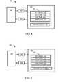
- FIG. 1is a block diagram of a data storage system in an embodiment of the present invention.
- FIG. 2is a memory array block diagram of the data storage system of FIG. 1 .
- FIG. 3is a memory map diagram of the data storage system of FIG. 1 .
- FIG. 4is an archive command flow diagram of the data storage system of FIG. 1 .
- FIG. 5is a restore command flow diagram of the data storage system of FIG. 1 .
- FIG. 6is a control flow of an archive process of the data storage system of FIG. 1 .
- FIG. 7is a control flow of a restore process of the data storage system of FIG. 1 .
- FIG. 8is a flow chart of a method of operation of the data storage system in a further embodiment of the present invention.
- modulecan include software, hardware, or a combination thereof in the context used herein.
- the softwarecan be machine code, firmware, embedded code, and application software.
- the hardwarecan be circuitry, processor, computer, integrated circuit, integrated circuit cores, a pressure sensor, an inertial sensor, a microelectromechanical system (MEMS), passive devices, or a combination thereof.
- MEMSmicroelectromechanical system
- the data storage system 100includes memory arrays 106 coupled to a controller 102 via a bus 104 .
- the controller 102is a processing unit for managing the storage and retrieval of data in the memory arrays 106 .
- the controller 102can be an embedded processor, control logic, or a combination thereof.
- the controller 102can transfer stored data from the memory arrays 106 to a host device 140 .
- the memory arrays 106are non-volatile memory units for storing data.
- the memory arrays 106can include NAND flash memory arrays, NOR flash memory arrays, other non-volatile memory arrays, or a combination thereof.
- the memory arrays 106can include a cell array 132 .
- the cell array 132is a set of non-volatile flash memory cells for storing data.
- the cell array 132can include a single-level cell flash memory (SLC), a multi-level cell flash memory (MLC), a mixed functionality cell, or a combination thereof.
- the memory arrays 106can include an array logic unit 130 coupled to the cell array 132 .
- the array logic unit 130is circuitry to provide addressing, data transfer and sensing, and other support to control the memory arrays 106 for saving and retrieving information from the cell array 132 .
- the controller 102can include a memory interface 116 coupled to the bus 104 .
- the memory interface 116can include circuitry for communicating with the memory arrays 106 over the bus 104 .
- the controller 102can include a control unit 110 coupled to the memory interface 116 and a host interface 114 .
- a read only memory 118can be coupled to the control unit 110 .
- a random access memory 120can be coupled to the control unit 110 and to the read only memory 118 .
- the random access memory 120can be utilized as a buffer memory for temporary storage of data being written to or read from the memory arrays 106 .
- the controller 102can include an error correction code unit 112 coupled to the control unit 110 .
- the error correction code unit 112is a processing hardware for calculating an error correction code value that can be used to detect errors, correct errors, or a combination thereof in data stored or transmitted from the memory arrays 106 .
- the error correction code unit 112can calculate one or more error correction code values using different methods including a Reed-Solomon code, a Hamming code, a Bose-Chauduri-Hocquenghem (BCH) code, low-density parity-check (LDPC), or a combination thereof.
- BCHBose-Chauduri-Hocquenghem
- LDPClow-density parity-check
- the error correction code unit 112is a dedicated element for calculating error correction codes, it is understood that error correction codes can also be calculated in other ways, such as using the control unit 110 to calculate error correction codes.
- the controller 102can include the host interface 114 coupled to the host device 140 .
- the host device 140is a computing device that can use the data storage system 100 for storing data.
- the host device 140can be a laptop computer, a server, a smart phone, or a combination thereof.
- the host interface 114can communicate commands and data between the host device 140 and the controller 102 for the operation of the data storage system 100 .
- the host interface 114can detect a connection to the host device 140 and generate command based on the connection to the host device 140 .
- Each of the memory arrays 106can include the cell array 132 of FIG. 1 and the array logic unit 130 of FIG. 1 .
- the memory arrays 106can include memory blocks 204 .
- the memory blocks 204are defined as portions of the memory arrays 106 for storing data that are the smallest addressable unit for erase operations.
- the memory arrays 106can be updated by erasing the memory blocks 204 and programming new data into the memory blocks 204 that have been erased. Programming the memory blocks 204 writes data into the memory blocks 204 .
- the memory blocks 204can include the memory pages 206 .
- the memory pages 206are defined as the smallest addressable units within the memory blocks 204 that can be used for reading and programming data.
- the memory arrays 106can have 4,096 of the memory blocks 204 with each of the memory blocks 204 having 64 of the memory pages 206 and each of the memory pages 206 .
- Data stored in the memory blocks 204has a data retention period 232 .
- the data retention period 232is defined as the length of time data written to the memory blocks 204 can be reliably read and recovered. Data retention can include the ability of a data bit to retain a data state over a period of time.
- Data stored in the memory blocks 204can fail to be reliably read because of a variety of data errors.
- data errorscan occur based on the age of the data stored, structural limitations of the memory technology used, read and write operations on neighboring memory locations, or a combination thereof.
- the data retention period 232can be influenced by a variety of factors. For example, the data retention period 232 can be determined based on the data retention of individual bits of data stored in the memory blocks 204 , the bit error rate of the memory arrays 106 , and the level of error correction coding used to detect and correct data errors.
- the memory blocks 204can be erased and programmed a finite number of cycles before becoming unable to reliably retain data.
- the memory blocks 204have a limited data endurance.
- Data enduranceis defined as a measure of the number of program and erase cycles one of the memory blocks 204 can sustain before being unable to reliably retain data.
- the data endurancecan be represented by a data endurance count 234 representing the estimated maximum number of program erase cycles the memory blocks 204 can be reliably programed and erased.
- the memory blocks 204can be associated with information about the configuration and status of the memory blocks 204 .
- the memory blocks 204can include information about the number of program and erase, error correction code information, redundancy information, or a combination thereof.
- Each of the memory blocks 204can include one or more of the memory pages 206 used to store configuration and status information.
- the memory blocks 204can include a program erase cycle count 224 .
- the program erase cycle count 224is the number of times one of the memory blocks 204 has been erased and programmed. Because flash memory has a limited number of cycles that it can be erased and programmed and still reliably store data, the program erase cycle count 224 can indicate the degree of usage for each of the memory blocks 204 .
- the memory blocks 204can include an error correction code 220 .
- the error correction code 220is defined as a calculated value used to detect errors, correct errors, or a combination thereof in the payload data.
- the error correction code 220can provided redundancy information that can be used to correct errors.
- the error correction code 220effectively increases the data retention period 232 as measured by the amount of time that the data of the memory blocks 204 can be reliably read by correcting data errors that may have occurred.
- the error correction code 220can be calculated for different types and portions of data including for the memory pages 206 , the memory blocks 204 , or a combination thereof.
- the error correction code 220can be stored in a variety of locations including the memory pages 206 , the memory blocks 204 , the memory arrays 106 , or a combination thereof.
- the memory arrays 106can include an overprovisioning area 230 .
- the overprovisioning area 230is defined as a portion of the memory arrays 106 that can be used for memory management and configuration.
- the overprovisioning area 230can be used for scratch pad memory, wear leveling, and spare memory for live replacement of unreliable memory.
- the overprovisioning area 230can be used for storing block information, the error correction code 220 , status information, bad block replacement, or a combination thereof.
- the size of the overprovisioning area 230can be the difference between the physical memory capacity of the data storage system 100 and the logical capacity available for storing payload data.
- the size of the overprovisioning area 230can be between 0%-28% of the overall memory size of the memory arrays 106 .
- a disk storage system 100 having a rated capacity of 100 GBcan include 28 GB in the overprovisioning area 230 .
- Each of the memory pages 206can include a data area 208 and a spare area 210 .
- the data area 208is defined as a portion of the memory pages 206 used to store payload data.
- Payload datacan include user data such as programs, images, video information, text, or a combination thereof.
- the spare area 210is defined as a portion of the memory pages 206 used to store information about the memory pages 206 .
- the spare area 210can include status and control information such as the error correction code information, page status flags 222 , or a combination thereof.
- the memory pages 206can include the page status flags 222 to represent the configuration and status of the memory pages 206 .
- the page status flags 222can include values indicating valid payload data, erasure status, erasure count, or a combination thereof.
- the memory pages 206can include fast pages 240 and slow pages 242 .
- fast pages 240can be represented with the most significant bits (MSB) and the least significant bits (LSB) of a floating gate cell of the multi-level cell flash memory.
- the fast pages 240can be the memory pages 206 that are associated with the most significant bit of the multi-level cell flash memory.
- the slow pages 242can be the memory pages associated with the least significant bit (LSB) of a multi-level cell flash memory.
- the fast pages 240 and the slow pages 242can be implemented in a variety of ways.
- a multi-level flash memory cellcan be associated with two of the memory pages 206 , one of the fast pages 240 and one of the slow pages 242 .
- the first time one of the fast pages 240 is written after being erasedthe page only needs to be written in a single operation.
- the current values of the multi-level cellshave to be read and then written back to update the values of the multi-level cell for both the fast pages 240 and the slow pages 240 .
- the time to write one of the fast pages 240can be on the order of 500 ⁇ s.
- the time to write one of the slow pages 242can be on the order of 1800 ⁇ s.
- the fast pages 240 of the multi-level cell flash memorycan operate similar to single-level cell flash memory by only writing payload data to the fast pages 240 and not writing to the slow pages 242 .
- Using only the fast pages 240can reduce the effective storage capacity 50%, but increase the data retention period 232 of the flash memory.
- the payload data of the flash memoryoccupies less than 50% of the storage capacity, the payload data can be archived by copying the payload data to only the fast pages 240 to increase data retention.
- the data of the memory pages 206 of the memory blocks 204can be protected using the error correction code 220 during read and write operations.
- the payload datacan be passed to the error correction code unit 112 of FIG. 1 and used to calculate the error correction code 220 to protect the payload data.
- the error correction code 220can be stored in the spare area 210 and associated with the payload data stored in the data area 208 .
- another of the error correction code 220can be calculated for the retrieved payload data and compared to the error correction code 220 that was originally stored with the payload data. If the two versions of the error correction code 220 are identical, then there are no data errors. If the two versions are different, then an error has occurred and the error correction code 220 can be used to correct the data error.
- the size and type of the error correction code 220can determine the number of data errors that can be detected, corrected, or a combination thereof. Stronger error correction code information can correct larger numbers of data errors and effectively increase the amount of time data can reliably be read by allowing the correction of more data errors over time. Error correction and detection can be strengthened by increasing the size of the error correction code 220 , utilizing a different type of code, combining multiple error correction codes for the same payload data, or a combination thereof.
- the error correction code 220can be concatenated to combine two or more different error correction codes to increase the level of error detection and correction and increase effective data retention.
- the memory blocks 204can be protected by the error correction code 220 utilizing a Reed Solomon code, a BCH code, and an LDPC.
- the error correction code 220can be calculated to accommodate specific conditions that may affect the number of data errors. In an illustrative example, if the data storage system 100 will be stored in a thermally hot storage location, such as in a military aircraft parked in the desert, then the type and size of the error correction code 220 can be configured to allow recovery from a larger number of data errors over a given time interval.
- the error correction code 220can be calculated at the time the payload data is stored using a BCH code that can correct up to 55 bit errors per 512 byte page.
- the ability to recover from a larger number of data errorscan allow the data to be recovered for a longer period of time resulting in longer effective data retention.
- Error correctioncan occur at different levels with the data storage system 100 .
- the error correction code 220can be calculated for the data of one of the memory pages 206 and can be stored in the spare area 210 of the memory pages 206 .
- the data storage system 100can include the error correction code 220 stored in other locations including the overprovisioning area 230 of the memory blocks 204 , other instances of the memory blocks 204 , other dissimilar non-volatile memory, or a combination thereof.
- the data storage system 100can include the error correction code 220 calculated for the data of the memory pages 206 and another of the error correction code 220 calculated for the data of the memory blocks 204 .
- the memory blocks 204can include a target block 212 .
- the target block 212is one of the memory blocks 204 that is available for writing new data.
- the target block 212is the intended destination of the next block of payload data to be written to the data storage system 100 .
- the target block 212can be selected from the available set of the memory blocks 204 not currently used to hold valid payload data.
- the memory blocks 204can include an erase block 214 .
- the erase block 214is the smallest portion of the flash memory that can be erased in a single operation.
- the erase block 214can be one of the memory blocks 204 memory blocks 204 identified as being available to be erased to make new storage space available.
- the erase block 214can be one of the memory blocks 204 that has recently been rewritten to the target block 212 and is no longer needed.
- the payload data stored in the memory blocks 204is normally configured to maximize the data endurance of the memory blocks 204 for routine usage. To facilitate longer term storage, the payload data stored in the memory blocks 204 can be archived to increase data retention.
- Archivingis defined reading and programming the payload data from one of the memory blocks 204 to another of the memory blocks 204 with storage settings configured to increase the amount of time the payload data can be reliably read.
- the data storage system 100can be archived by reading all of the payload data and writing the payload data to new memory locations in the memory blocks 204 .
- the payload data stored in the memory blocks 204can include a pre-archived data block 216 .
- the pre-archived data block 216is one of the memory blocks 204 having stored payload data before it has been archived.
- the pre-archived data block 216can include payload data that has been programmed in one of the memory blocks 204 with storage settings configured to increase the total number of program and erase cycles for the memory blocks 204 .
- the memory blocks 204can include an archived data block 218 .
- the archived data block 218is one of the memory blocks 204 having payload data that has already been archived to increase the amount of time the payload data can be reliably read.
- the archived data block 218has been programmed to increase data retention.
- the payload data in the archived data block 218can be restored to another of the memory blocks 204 to refresh the data and increase data endurance.
- Restoringis defined reading the payload data in the archived data block 218 and programming the target block 212 with storage settings configured to increase the maximum number of program and erase cycles of the target block 212 .
- the archived data block 218represents the payload data on the data storage system 100 after it has been archived for maximum data retention.
- the data storage system 100can include the memory blocks 204 having a logical to physical table 302 and an erase block pool 310 .
- the data storage system 100can include the logical to physical table 302 for mapping a logical block address 304 to a physical block address 306 .
- the logical to physical table 302allows mapping the logical blocks to different physical blocks as the data in one of the memory blocks 204 is moved or copied to a different location in the memory arrays 106 of FIG. 1 .
- the data storage system 100can include the erase block pool 310 .
- the erase block pool 310is defined as a set of the memory blocks 204 that have been erased to provide storage space for new data to be written.
- the erase block pool 310is a dynamic list and can grow and shrink as the memory blocks 204 are no longer needed after being copied or updated in another of the memory blocks 204 .
- the pre-archived data block 216 of FIG. 2when the data of the pre-archived data block 216 of FIG. 2 is read and programmed to the target block 212 of FIG. 2 , the pre-archived data block 216 can be identified as no longer containing valid data. Only the memory blocks 204 having valid payload data stored in the memory pages 206 are archived and rewritten. The pre-archived data block 216 can be recycled by erasing the pre-archived data block 216 and tagging the pre-archived data block 216 as the erase block 214 .
- the erase block 214 of FIG. 2can be assigned to the erase block pool 310 for later use.
- the archive command flow diagram 401can depict command and message flow between the host device 140 and the data storage system 100 for an archive command 402 .
- the archive command 402is an instruction to the data storage system 100 to preserve the payload data for maximum data retention.
- the data storage system 100can receive the archive command 402 sent by the host device 140 . After receiving the archive command 402 , the data storage system 100 can set an archive status 420 to indicate that the execution of the archive command 402 has been initiated. For example, the archive status 420 can be set to “Archive in progress”. The archive status 420 can represent the state of the data storage system 100 .
- the data storage system 100can begin archiving the payload data in the memory arrays 106 of FIG. 1 by copying the payload data to new memory locations to increase data retention by refreshing the data. Copying is defined as reading the payload data and programming the payload data in the new memory locations.
- the archive status 420can be set to indicate that the archive command 402 has completed. For example, the archive status 420 can be set to “Archive complete”.
- the data storage system 100can insure completion by restarting the execution of the archive command 402 if process is interrupted.
- the execution of the archive command 402can be interrupted if the data storage system 100 is removed from the host device 140 .
- the archive status 420can be checked and if the archive status 420 indicates that the execution of the archive command 402 has not been completed, then the execution of the archive command 402 can be restarted.
- the archive status 420can be checked each time the data storage system 100 is reconnected to the host device 140 until the archive status 420 indicated that all of the payload data has been archived. To insure data integrity, the data storage system 100 can prevent access to the payload data until the archive status 420 indicates the completion of the execution of the archive command 402 .
- the data storage system 100can archive data by copying the data of the pre-archived data block 216 of FIG. 2 to the target block 212 of FIG. 2 to refresh the data.
- the data storage system 100can update the archive status 420 stored in non-volatile memory to indicate the data has been archived and send an archive status message 404 to the host device 140 .
- the archive status message 404can include the archive status 420 .
- the data storage system 100can include a set of commands for transferring and managing data.
- the set of commandscan include an erase a block command, a program a page command, a copy a block command, read a page command, or a similar command.
- the data storage system 100can include command settings 410 used to modify the storage of data.
- the command settings 410are defined as control values that can alter the behavior and operation of the commands executed on the data storage system 100 .
- the command settings 410can include a program erase threshold 412 , an error correction code level 414 , a storage temperature 416 , command flags 418 , or other information for controlling the storage and retrieval of data.
- the program erase threshold 412can represent a limit of the number of program and erase (PE) cycles of the memory blocks 204 of FIG. 2 for use in the archival of data. For example, if the target block 212 has the program erase cycle count 224 of FIG. 2 greater than or equal to the program erase threshold 412 , then the target block 212 can be replaced with another one of the memory blocks 204 with the program erase cycle count 224 having a lower value.
- PEprogram and erase
- the error correction code level 414is a value to specify the type and size of the error correction codes used during the reading and programming of data.
- the error correction code level 414can be used to expressly override the default error correction code used by the data storage system 100 .
- the error correction code level 414can be set to indicate a BCH error correction code should be calculated for each of the memory pages 206 of FIG. 2 .
- the storage temperature 416is the expected storage temperature of the data storage system 100 after archival of the data.
- the storage temperature 416can represent a single storage temperature or a temperature range.
- the storage temperature 416can be used as a factor to estimate the potential data error rate of the environment where the data storage system 100 will be stored, such as a thermally hot environment. For example, if the storage temperature 416 is 55 degrees Celsius, then the data storage system 100 can compensate for the higher temperature by using a stronger error correction coding, such as a longer BCH code, when archiving data to compensate for the potentially higher data error rate. In another example, the bit error rate of the data storage system 100 can increase by a factor of five to ten as the storage temperature increases from 40 degrees Celsius to 55 degrees Celsius.
- the command flags 418can represent control information for modifying the operational characteristics of the data storage system 100 .
- the command flags 418can be used to modify the timing, duration, and voltage levels of control signals used to read, store, and erase data in the memory arrays 106 .
- the command flags 418can be modified to control the voltage level used when erasing one of the memory blocks 204 to enhance data retention by imparting a higher level of charge in the floating gate transistors of the cell arrays 132 of FIG. 1 .
- the command flags 418can be used to control the duration of write signals to the cell arrays 132 .
- the data retention period 232can be increased by determining the bit error rate calculated by the error correction code unit 112 of FIG. 1 when writing to the target block 212 .
- the command flags 418can be modified to change a read threshold to improve the bit error rate.
- the command flags 418can be modified to adjust the read threshold to reduce the bit error rate to be correctable by the error correction code unit 232 implementing the error correction code level 414 .
- the restore command flow diagram 501can depict command and message flow between the host device 140 and the data storage system 100 for a restore command 502 .
- the restore command 502is an instruction to the data storage system 100 to restore the archived data to the memory blocks 204 optimized for maximum data endurance.
- the data storage system 100can receive the restore command in a variety of ways.
- the data storage system 100can receive the restore command 502 from the host device 140 to initiate the restore process.
- the data storage system 100can automatically generate the restore command 502 when the data storage system 100 detects the connection to the host device 140 .
- the data storage system 100can trigger the restore command 502 when it receives operating electrical power.
- the data storage system 100can set a restore status 520 to indicate that the execution of the restore command has been initiated.
- the restore status 520can be set to “Restore in progress”.
- the restore status 520can represent the state of the data storage system 100 .
- the data storage system 100can insure completion by restarting the execution of the restore command 502 if process is interrupted.
- the execution of the restore command 502can be interrupted if the data storage system 100 is removed from the host device 140 .
- the restore status 520can be detected and if the restore status 520 indicates that the execution of the restore command 502 has not completed, then the execution of the restore command 502 can be restarted.
- the restore status 520can be checked each time the data storage system 100 is reconnected to the host device 140 until the restore status 420 indicates that all of the archived data has been restored. To insure data integrity, the data storage system 100 can prevent access to the payload data until the restore status 520 indicates the completion of the execution of the restore command 502 .
- the data storage system 100can restore the archived data in the memory blocks 204 of FIG. 2 by copying the archived payload data to new memory locations using the command settings 410 to maximize data endurance.
- Restoring datais performed by reading the archived payload data in the archived data block 218 of FIG. 2 and programming the target block 212 of FIG. 2 with the archived payload data using the command settings 410 that have been configured to maximize data endurance.
- the data storage system 100can include the command settings 410 used to modify the storage and retrieval of data.
- the command settings 410can include the program erase threshold 412 , the error correction code level 414 , the storage temperature 416 , the command flags 418 , or other information for controlling the archiving and restoration of data.
- the data storage system 100can update the restore status 520 indicate the data has been restored.
- the restore status 520can be set to “Restore complete”.
- the data storage system 100can send a restore status message 504 to the host device 140 to indicate that the data storage system 100 has been restored and is ready for regular operation.
- the restore status message 504can include the restore status 520 .
- the archive process 601can preserve the data of the data storage system 100 by copying the data of the pre-archived data block 216 of FIG. 2 to new data locations.
- the archive process 601can receive the archive command 402 of FIG. 4 from the host device 140 of FIG. 1 in a receive archive command module 602 .
- Receiving the archive commandcan prepare the data storage system 100 of FIG. 1 to copy the existing payload data to new blocks on the data storage system 100 to maximize data retention.
- the receive archive command module 602can check and define the state of the data storage system 100 by adjusting the archive status 420 of FIG. 4 and the restore status 520 of FIG. 5 .
- the archive status 420can be set to “Archive in progress” to indicate that archive process 601 has been started and the restore status 520 can be set to a blank value.
- the control flow of the archive process 601can proceed to a set erase retention module 604 .
- the set erase retention module 604can configure the command settings 410 of FIG. 4 for the erase command to maximize the data retention period 232 of FIG. 2 .
- Data retentioncan be optimized without regards for data endurance.
- the execution of the erase commandcan erase the memory blocks 204 of FIG. 2 of the data storage system 100 to prepare for programming the memory blocks 204 with new data.
- the set erase retention module 604can configure the erase command to maximize the data retention period 232 in a variety of ways.
- the command settings 410can include the command flags 418 of FIG. 4 set to maximize the data retention period 232 by modifying the configuration of the erase block pool 310 of FIG. 3 .
- the command flags 418can indicate that the erase block 214 of FIG. 2 having the program erase cycle count 224 of FIG. 2 with the lowest value can be positioned at the beginning of the erase block pool 310 .
- the erase block pool 310can be effectively sorted to allow the memory blocks 204 with the lowest number of program erase cycle count 224 to be assigned to the beginning of the erase block pool 310 .
- the target block 212 of FIG. 2 selected from the beginning of the erase block pool 310can have the program erase cycle count 224 with a lower value and thus better data retention.
- the command settings 410can be configured to insert the erase block 214 having the program erase cycle count 224 with higher values at the end of the erase block pool 310 .
- the command settings 410can include the command flags 418 configured to maximize the data retention period 232 by modifying the operational characteristics used during the execution of the erase command.
- the command settings 410can be configured to modify the command flags 418 to increase the duration of the erase pulse to increase the amount of charge stored in the cell array 132 of FIG. 1 on erase. By increasing the amount of charge in the cell array 132 , the data stored in the cell array 132 can be retained for a longer period.
- the command settings 410can be configured to maximize the data retention period 232 by identifying the memory blocks 204 having the program erase cycle count 224 greater than or equal to the program erase threshold 412 of FIG. 4 .
- the memory blocks 204 exceeding the program erase threshold 412can be eliminated from the erase block pool 310 and not used when rewriting the pre-archived data block 216 . Avoiding recycling the memory blocks 204 with the program erase cycle count 224 above the program erase threshold 412 can prevent the use of the memory blocks 204 having poor data retention performance due to excessive use and higher wear.
- the command settings 410can be configured to modify the error correction code level 414 of FIG. 4 to maximize the data retention period 232 by erasing the target block 212 and configuring the target block 212 for a stronger level of error correction coding to be stored in the overprovisioning area 230 of FIG. 2 .
- the payload data stored in the target block 212can be reliably read for a longer period of time by allowing for correction of data errors that occur over time.
- the target block 212can be erased and additional space in the overprovisioning area 230 can be allocated to accommodate the error correction code 220 of FIG. 2 having a greater length.
- the overprovisioning area 230can be configured to store and associate the error correction code 220 having a greater minimum distance, such as a 55 bit BCH code.
- the control flowcan proceed to a set program retention module 606 .
- the set program retention module 606can configure the command settings 410 for the program command to maximize the data retention period 232 .
- the execution of the program commandcan write data to the target block 212 .
- the command settings 410can be configured to maximize the data retention period 232 during the program command in a variety of ways.
- the command settings 410can be configured to maximize the data retention period 232 by setting the command flags 418 to indicate that the payload data should be distributed across the maximum number of the memory blocks 204 .
- Distributing the payload datacan include copying the data of the memory pages 206 of FIG. 2 of the pre-archived data block 216 to two or more instances of the target block 212 .
- the command settings 410can be configured to maximize the data retention period 232 by setting the command flags 418 to indicate that the payload data should be stored in only the fast pages 240 of FIG. 2 of the target block 212 .
- the fast pages 240are associated with the most significant bit of the multi-level cell flash memory.
- the fast pages 240 pagescan represent data with large discrete charge levels that result in larger values for the data retention period 232 .
- the command settings 410can be configured to maximize the data retention period 232 by increasing the error correction code level 414 when programming the target block 212 with data.
- the error correction code level 414can indicate that a 64-bit Reed-Solomon code should be calculated to protect the payload data. It is understood that the error correction code level 414 can indicate the size and type of error correction coding.
- the error correction code level 414can indicate that a 55 bit BCH code should be used. In yet another example, the error correction code level 414 can indicate that a Reed-Solomon code and a BCH code should be used and concatenated together.
- the error correction code level 414can be adjusted based on the type of data errors detected by the data storage system 100 .
- the error correction code level 414can be set based on the data error type, such as burst error distribution, random error distribution, or a combination thereof.
- Matching the error correction code level 414 to the type of data errorscan increase the data retention period 232 of the target block 212 .
- setting the error correction code level 414 to indicate a Reed-Solomon codecan optimize for burst errors.
- setting the error correction code level 414 to indicate a BCH codecan optimize for random data errors.
- the error correction code level 414can be adjusted based on the characteristics of the data errors including the direction of the bit errors. Bit errors move in one direction, either changing from binary 0 to binary 1 or changing from binary 1 to binary 0.
- the error correction code level 414can be set to indicate an error correction code to take advantage of the direction of the bit error changes.
- the error correction code 220 of FIG. 2can be stored in the spare area 210 of FIG. 2 during the archive process 601 .
- the error correction code 220can also be stored in the overprovisioning area 230 of FIG. 2 .
- the command settings 410can be configured to use different operational characteristics during the execution of the program command by setting the command flags 418 of FIG. 4 to select longer write duration and timing, higher programming voltages, single plane operation, or a combination thereof.
- the command settings 410can be configured to modify the command flags 418 to alter the duration of the program pulse to reduce the amount of charge stored in the cell array 132 during the program command.
- the command flags 418can be configured to indicate single plane operation for archiving the payload data.
- the cell arrays 132 of FIG. 1can be partitioned into different planes, where each plane is a subset of the memory arrays 106 of FIG. 1 that can be accessed independently.
- the data storage system 100can operate using multi-plane operations for better bandwidth, improved simultaneous data transfer performance, and reduced runtime power consumption.
- multi-plane operationcan cause an increase in the bit error rate and an increased failure rate of the flash. Setting the command flags 418 for single plane operation can improve the data retention period 232 and reduced the number of data errors.
- the control flow of the archive process 601can proceed to an archive status check module 608 to determine if all of the payload data on the data storage system 100 has all been archived. If the archive status check module 608 indicates that all data has been successfully archived, then control flow passes to an update archive status module 618 .
- the update archive status module 618can update the archive status 420 of FIG. 4 of the data storage system 100 by setting the archive status 420 to indicate that all of the data has been copied to new locations.
- the control flowcan pass to a send archive complete module 620 .
- the send archive complete module 620can send the archive status message 404 of FIG. 4 to the host device 140 via the host interface 114 of FIG. 1 of the data storage system 100 .
- the archive status message 404can inform the host device 140 that the archive process 601 has completed and the data storage system 100 can be safely removed and stored.
- the control flowcan pass to an erase target block module 610 .
- the erase target block module 610can identify the target block 212 and erase the target block 212 using the command settings 410 configured to maximize data retention.
- the erase target block module 610can identify the target block 212 in a variety of ways.
- the target block 212can be assigned to the erase block 214 at the beginning of the erase block pool 310 .
- the erase target block module 610initiates a garbage collection process to recover the memory blocks 204 previously identified as unused to add to the erase block pool 310 .
- the erase block pool 310can be updated by adding the erase block 214 at the top of the list and assigning the erase block 214 to be the target block 212 .
- the target block 212can be erased using the erase command with the command settings 410 configured to maximize data retention.
- the target block 212can be erased and all of the data bits of the target block 212 can be set to 1.
- the control flow of the archive process 601can proceed to a read pre-archived data module 612 .
- the read pre-archived data module 612can identify the pre-archived data block 216 to be rewritten to the target block 212 .
- the pre-archived data block 216is defined as one of the memory blocks 204 of the payload data stored on the data storage system 100 .
- the pre-archived data block 216can be read in a variety of ways. For example, the data can be retrieved from the pre-archived data block 216 and buffered in the random access memory 120 of FIG. 1 . In another example, the pre-archived data block 216 can be identified from the list of the memory blocks 204 of the payload data and flagged as the pre-archived data block 216 .
- the control flow of the archive process 601can proceed to a write pre-archived data module 614 .
- the write pre-archived data module 614can write the pre-archived data block 216 to the target block 212 with the command settings 410 configured to maximize the data retention period 232 .
- the target block 212can be configured as a high retention block that has been configured to maximize data retention.
- the logical to physical table 302 of FIG. 3can be updated to replace the physical block address of the pre-archived data block 216 with the physical block address of the target block 212 .
- the pre-archived data block 216can be written to the target block 212 in a variety of ways.
- the pre-archived data block 216can be written to the target block 212 from the random access memory 120 using the program command with command settings 410 configured to maximize the data retention period 232 .
- the data of the pre-archived data block 216can be written to the target block 212 using an internal copy command optimized for data retention.
- the execution of the internal copy commandcan copy the data of the pre-archived data block 216 directly from the pre-archived data block 216 in the memory arrays 106 of FIG. 1 to the target block 212 in the memory arrays 106 without transferring the data out of the memory arrays 106 .
- the control flow of the archive process 601can proceed to a recycle pre-archived data module 616 .
- the recycle pre-archived data module 616can recycle the pre-archived data block 216 by tagging the pre-archived data block 216 as not having valid data, erasing the pre-archived data block 216 , and adding the pre-archived data block 216 to the erase block pool 310 .
- the control flow of the archive process 601can proceed back to the archive status check module 608 .
- the archive process 601can form a loop for checking the archive status 420 , reading the data of the pre-archived data block 216 , writing the data of the pre-archived data block 216 to the target block 212 , and recycling the copied instances of the pre-archived data block 216 .
- the loopcan continue until all of the payload data has been archived. If the archive process 601 is interrupted, the next time the archive process 601 begins, the archive status 420 can be check to determine if the archive process 601 should be continued.
- the present inventionprovides improved data retention for the storage of payload data of the memory blocks 204 during the archive process by distributing the payload data across the maximum number of the memory blocks 204 .
- the data retention period 232is increased due to the reduction in data errors due to bit flipping caused by writing data in neighboring memory cells.
- the present inventionprovides improved data retention for the storage of payload data of the memory blocks 204 of the memory arrays 106 during the archive process by copying the data of the pre-archived data block 216 to the target block 212 using the command settings 410 configured to maximize data retention.
- the target block 212will be refreshed and have a longer data retention period 232 .
- the present inventionprovides improved data retention time for storage of the payload data of the memory blocks 204 of the memory arrays 106 by increasing the level of error correction associated with each of memory pages 206 of the memory blocks 204 .
- the enhanced error correctioncan provide increased effective data retention time by detecting and correcting data errors in the memory blocks 204 .
- the present inventionprovides an improved data retention period for the storage of the payload data of the memory blocks 204 by adjusting the error correction code level 414 to accommodate the type of data errors detected. By matching the error correction code level 414 to deal with different types of data errors, the data retention period 232 can be increased.
- the present inventionprovides improved data integrity during storage by copying the data of the memory blocks 204 of the memory arrays 106 to new locations to maximize the data retention period 232 .
- Archiving the payload data stored in the memory blocks 204can mitigate the effect of data errors that occur based on the age of data, temperature, read disturb errors, and errors due to the base level of data retention of the memory arrays 106 .
- the restore process 701can preserve the data of the data storage system 100 by copying the data of the archived data block 218 of FIG. 2 to the target block 212 of FIG. 2 with the command settings 410 of FIG. 4 configured to maximize the data endurance count 234 of FIG. 2 of the target block 212 .
- the restore process 701can receive the restore command 502 of FIG. 5 from the host device 140 of FIG. 1 in a receive restore command module 702 .
- the receive restore command module 702can detect the current state of the data storage system 100 and restart the restore process 701 if the restore status 520 indicate that the restore process 701 is in progress.
- Receiving the restore command 502can prepare the data storage system 100 to copy the archived data to new blocks on the data storage system 100 to refresh the data for maximizing data endurance.
- the receive restore command module 702can define the state of the data storage system 100 by adjusting the restore status 520 of FIG. 5 and the archive status 420 of FIG. 4 .
- the restore status 520can be set to “Restore in progress” to indicate that restore process 701 has been started and the archive status 420 can be set to a blank value.
- the restore command 502can also be automatically generated when the data storage system 100 is connected to the host device 140 of FIG. 1 .
- the controller 102 of FIG. 1can detect the host device 140 via the host interface 114 of FIG. 1 and generate the restore command 502 automatically.
- the restore process 701can be automatically restarted if the host device 140 has been disconnected and then reconnected if the restore status 520 indicates that the restore process has not finished.
- the restore process 701includes copying the data of all of the memory blocks 204 of FIG. 2 previously optimized for data retention and rewriting the memory blocks 204 to the data storage system 100 with the command settings 410 configured to maximize data endurance.
- the restore process 701can continue and be restarted until all data has been restored.
- the control flow of the restore process 701can proceed to a set erase endurance module 704 .
- the set erase endurance module 704can configure the command settings 410 for maximum data endurance. Data endurance can be optimized without regard for data retention.
- the execution of the erase commandcan erase the memory blocks 204 of the data storage system 100 to prepare for programming the memory blocks 204 with new data.
- the set erase endurance module 704can configure the erase command to maximize the data endurance count 234 of the erase command in a variety of ways.
- the command settings 410can be configured to maximize the data endurance count 234 by modifying the configuration of the erase block pool 310 of FIG. 3 such that the erase block 214 of FIG. 2 having the program erase cycle count 224 of FIG. 2 with the lowest value is positioned at the beginning of the erase block pool 310 .
- the erase commandcan be configured to insert the erase block 214 having the program erase cycle count 224 with higher values at the end of the erase block pool 310 .
- the command settings 410can be configured to maximize the data endurance count 234 by modifying the command flags 418 of FIG. 4 to change the operational characteristics used during the execution of the erase command.
- the command settings 410can be configured to change the duration of the program pulse to reduce the amount of charge stored in the cell array 132 of FIG. 1 on erase to increase data endurance of the cell array 132 .
- the command settings 410can be configured to maximize the data endurance count 234 by preparing the target block 212 for a level of error correction code data commensurate with normal data endurance operation. Preparing the target block 212 can include freeing memory space for the error correction codes in the overprovisioning area 230 of FIG. 2 and limiting the storage of the error correction code 220 of FIG. 2 to the memory pages 206 of FIG. 2 . By altering the level of error correction coding, the data stored in the target block 212 can increase the data endurance count 234 of the target block 212 .
- the control flow of the restore process 701can proceed to a set program endurance module 706 .
- the set program endurance module 706can configure the command settings 410 to maximize the data endurance count 234 of the program command in a variety of ways.
- the command settings 410can be configured by setting the command flags 418 to indicate that the payload data should be distributed across the minimum number of the memory blocks 204 .
- Distributing the payload datacan include copying the data of the memory pages 206 of the two or more of the archived data block 218 to the target block 212 .
- the command settings 410can be configured by setting the command flags 418 to indicate that the payload data should be stored equally across the memory pages 206 of the target block 212 without regard to fast or slow page status.
- the overall number of the memory blocks 204 needed to store the payload datacan be reduced. Using fewer of the memory blocks 204 can reduce the total number of program and erase cycles, and reduce the impact on the data endurance count 234 .
- the command settings 410can be configured by setting the error correction code level 414 of FIG. 4 to the default level of error correction.
- the error correction code level 414can indicate that the error correction code unit 112 of FIG. 1 should use a 55-bit BCH code.
- the command settings 410can be configured to maximize the data endurance count 234 by setting the command flags 418 of FIG. 4 to select the duration and timing, default programming voltages, plane operation, or a combination thereof for maximum endurance.
- the command settings 410can be set to maximize the data endurance count 234 without regard for the impact of data retention.
- the command flags 418can be configured to implement multi-plane operation for restoring the archived payload data.
- the data storage system 100can operate using multi-plane operations for better bandwidth, data transfer performance, and reduced runtime power consumption. However, multi-plane operation can cause an increase in the bit error rate and an increased failure rate of the flash. Setting the command flags 418 for multi-plane operation can improve the data endurance count 234
- the control flow of the restore process 701can proceed to a restore status check module 708 to determine if all of the data on the data storage system 100 has been restored. If the restore status check module 708 indicates that all data has been successfully restored, then control flow passes to an update restore status module 718 .
- the update restore status module 718can update the restore status 520 of the data storage system 100 by setting the restore status to indicate all of the data has been restored.
- the control flowcan pass to a send restore complete module 720 .
- the send restore complete module 720can send a restore status message to the host device 140 via the host interface 114 of the data storage system 100 .
- the restore status message 504 of FIG. 5can inform the host device 140 that the restore process 701 has completed and the data storage system 100 can be safely used.
- the erase restore target block module 710can identify the target block 212 and erase the target block 212 using the command settings 410 configured to maximize data endurance.
- the erase restore target block module 710can identify the target block 212 in a variety of ways.
- the target block 212can be assigned to be the erase block 214 at the top of the erase block pool 310 .
- the erase restore target block module 710can initiate a garbage collection process to recover the memory blocks 204 previously identified as unused to add to the erase block pool 310 .
- the erase block pool 310can be updated by adding the erase block 214 at the top of the list and assigning the erase block 214 to be the target block 212 . Recovering the memory blocks 204 is defined as adding the memory blocks 204 to the erase block pool 310 .
- the target block 212can be erased using the command settings 410 configured to maximize data endurance.
- the target block 212can be erased and all of the data bits of the target block 212 can be set to 1.
- the control flow of the restore process 701can proceed to a read archived data module 712 .
- the read archived data module 712can identify the archived data block 218 to be programmed to the target block 212 .
- the archived data block 218is defined as one of the memory blocks 204 containing payload data that has been archived for maximum data retention.
- the archived data block 218can be read in a variety of ways.
- the archived data block 218can be retrieved and buffered in the random access memory 120 of FIG. 1 .
- the archived data block 218can be identified from the list of the memory blocks 204 of the payload data and flagged as the archived data block 218 .
- the control flow of the archive process 601 of FIG. 6can proceed to a write archived data module 714 .
- the write archived data module 714can write the archived data block 218 to the target block 212 with the command settings 410 configured to maximize data endurance.
- the target block 212can be configured as a high endurance block that has been optimized for data endurance.
- the archived data block 218can be written to the target block 212 in a variety of ways.
- the archived data block 218can be written to the target block 212 from the random access memory 120 using the program command with the command settings 410 configured to maximize data endurance.
- the logical to physical table 302 of FIG. 3can be updated to replace the physical block address of the archived data block 218 with the physical block address of the target block 212 .
- the archived data block 218can be written to the target block 212 using an internal copy command optimized for data endurance.
- the execution of the internal copy commandcan copy the data of the archived data block 218 directly from the archived data block 218 in the memory arrays 106 to the target block 212 in the memory arrays 106 without transferring the data out of the memory arrays 106 .
- the control flow of the restore process 701can proceed to a recycle archived data module 716 .
- the recycle archived data module 716can recycle the archived data block 218 by tagging the archived data block 218 of FIG. 2 as invalid and adding the archived data block 218 to the erase block pool 310 .
- the control flow of the restore process 701can proceed back to the restore status check module 708 .
- the restore process 701can form a loop for checking the restore status 520 , reading the data of the archive block memory blocks, writing the data of the archived data block 218 to the target block 212 , and recycling the copied instances of the archived data block 218 .
- the loopcan continue until all of the archived payload data has been restored.
- the restore process 701can be interrupted by disconnecting the data storage system 100 from the host device 140 .
- the data storage system 100can restart the restore process 701 when reconnected to the host device 140 by detecting the connection the host device 140 and automatically generating the restore command 502 .
- the restore process 701can be restarted by applying power to the data storage system 100 and examining the restore status 520 .
- the restore status 520can be stored in non-volatile memory, for example in the overprovisioning area 230 .
- the present inventionprovides improved data endurance for the storage of payload data of the memory blocks 204 by restoring the archived data block 218 to the minimum number of the memory blocks 204 needed to hold the payload data. By reducing the total number of memory blocks 204 , the number of program and erase cycles is minimized, reducing the overall effect on the data endurance of the memory blocks 204 .
- the present inventionprovides improved data endurance time for the storage of the payload data of the memory blocks 204 of the memory arrays 106 during the restore process by copying the data of the archived data block 218 to the target block 212 using the command settings 410 configured to maximize data endurance.
- the target block 212will be refreshed and can have a longer data endurance time.
- the present inventionprovides improved data safety by automatically restarting the restore process 701 when the data storage system 100 receives power or is reconnected to the host device 140 .
- the host device 140can be provided with a valid set of data when the host device 140 receives the restore status message 504 of FIG. 5 .
- the present inventionprovides improved data endurance and improved effective operation lifetime by restoring the archived data block 218 to the target block 212 with the command settings 410 configured to maximize data endurance in the restore process 701 .
- the effective operational lifetime of the data storage system 100can be increased.
- the method 800includes: identifying a target block in a block 802 ; configuring a command setting for maximizing a data retention period of the target block in a block 804 ; writing a pre-archived memory block to the target block based on the command setting in a block 806 ; and updating an archive status for sending to a host device in a block 808 .
- the data storage system of the present inventionfurnishes important and heretofore unknown and unavailable solutions, capabilities, and functional aspects for data storage system configurations.
- the resulting processes and configurationsare straightforward, cost-effective, uncomplicated, highly versatile, accurate, sensitive, and effective, and can be implemented by adapting known components for ready, efficient, and economical manufacturing, application, and utilization.
- Another important aspect of the present inventionis that it valuably supports and services the historical trend of reducing costs, simplifying systems, and increasing performance. These and other valuable aspects of the present invention consequently further the state of the technology to at least the next level.
Landscapes
- Engineering & Computer Science (AREA)
- Theoretical Computer Science (AREA)
- Physics & Mathematics (AREA)
- General Engineering & Computer Science (AREA)
- General Physics & Mathematics (AREA)
- Techniques For Improving Reliability Of Storages (AREA)
Abstract
Description
Claims (22)
Priority Applications (1)
| Application Number | Priority Date | Filing Date | Title |
|---|---|---|---|
| US13/433,090US8935466B2 (en) | 2011-03-28 | 2012-03-28 | Data storage system with non-volatile memory and method of operation thereof |
Applications Claiming Priority (2)
| Application Number | Priority Date | Filing Date | Title |
|---|---|---|---|
| US201161468483P | 2011-03-28 | 2011-03-28 | |
| US13/433,090US8935466B2 (en) | 2011-03-28 | 2012-03-28 | Data storage system with non-volatile memory and method of operation thereof |
Publications (2)
| Publication Number | Publication Date |
|---|---|
| US20120254519A1 US20120254519A1 (en) | 2012-10-04 |
| US8935466B2true US8935466B2 (en) | 2015-01-13 |
Family
ID=46928861
Family Applications (1)
| Application Number | Title | Priority Date | Filing Date |
|---|---|---|---|
| US13/433,090Expired - Fee RelatedUS8935466B2 (en) | 2011-03-28 | 2012-03-28 | Data storage system with non-volatile memory and method of operation thereof |
Country Status (1)
| Country | Link |
|---|---|
| US (1) | US8935466B2 (en) |
Cited By (2)
| Publication number | Priority date | Publication date | Assignee | Title |
|---|---|---|---|---|
| US20150178152A1 (en)* | 2013-12-20 | 2015-06-25 | Lsi Corporation | Preventing programming errors from occurring when programming flash memory cells |
| US9846554B1 (en)* | 2016-08-04 | 2017-12-19 | Sandisk Technologies Llc | Storage system and method for grouping blocks based on deterministic data patterns |
Families Citing this family (20)
| Publication number | Priority date | Publication date | Assignee | Title |
|---|---|---|---|---|
| WO2011013351A1 (en)* | 2009-07-30 | 2011-02-03 | パナソニック株式会社 | Access device and memory controller |
| US9170744B1 (en) | 2011-04-06 | 2015-10-27 | P4tents1, LLC | Computer program product for controlling a flash/DRAM/embedded DRAM-equipped system |
| US8930647B1 (en) | 2011-04-06 | 2015-01-06 | P4tents1, LLC | Multiple class memory systems |
| US9176671B1 (en) | 2011-04-06 | 2015-11-03 | P4tents1, LLC | Fetching data between thread execution in a flash/DRAM/embedded DRAM-equipped system |
| US9164679B2 (en) | 2011-04-06 | 2015-10-20 | Patents1, Llc | System, method and computer program product for multi-thread operation involving first memory of a first memory class and second memory of a second memory class |
| US9158546B1 (en) | 2011-04-06 | 2015-10-13 | P4tents1, LLC | Computer program product for fetching from a first physical memory between an execution of a plurality of threads associated with a second physical memory |
| US9417754B2 (en) | 2011-08-05 | 2016-08-16 | P4tents1, LLC | User interface system, method, and computer program product |
| US8694754B2 (en)* | 2011-09-09 | 2014-04-08 | Ocz Technology Group, Inc. | Non-volatile memory-based mass storage devices and methods for writing data thereto |
| US8966343B2 (en)* | 2012-08-21 | 2015-02-24 | Western Digital Technologies, Inc. | Solid-state drive retention monitor using reference blocks |
| US9367391B2 (en) | 2013-03-15 | 2016-06-14 | Micron Technology, Inc. | Error correction operations in a memory device |
| US8908443B1 (en) | 2014-05-27 | 2014-12-09 | Sandisk Technologies Inc. | Storage device and method for performing a self-refresh operation |
| US9443617B2 (en) | 2014-07-18 | 2016-09-13 | Kabushiki Kaisha Toshiba | Memory system and method of controlling memory system |
| KR102276374B1 (en)* | 2015-01-09 | 2021-07-14 | 삼성전자주식회사 | SEMICONDUCTOR PACKAGE WITH PoP STRUCTURE AND THEREFORE REFRESH CONTROL METHOD |
| US11294588B1 (en)* | 2015-08-24 | 2022-04-05 | Pure Storage, Inc. | Placing data within a storage device |
| US10248515B2 (en)* | 2017-01-19 | 2019-04-02 | Apple Inc. | Identifying a failing group of memory cells in a multi-plane storage operation |
| US10289548B1 (en)* | 2017-04-28 | 2019-05-14 | EMC IP Holding Company LLC | Method and system for garbage collection in a storage system which balances wear-leveling and performance |
| KR102640951B1 (en)* | 2018-11-22 | 2024-02-26 | 에스케이하이닉스 주식회사 | Memory controller and operating method thereof |
| US10983717B1 (en)* | 2020-05-01 | 2021-04-20 | EMC IP Holding Company LLC | Uninterrupted block-based restore using a conditional construction container |
| US11695552B2 (en)* | 2021-03-25 | 2023-07-04 | International Business Machines Corporation | Quantum key distribution in a multi-cloud environment |
| KR20240162213A (en)* | 2023-05-08 | 2024-11-15 | 에스케이하이닉스 주식회사 | Storage device migrating user data stored on memory die in an unusable state and operating method of the storage device |
Citations (165)
| Publication number | Priority date | Publication date | Assignee | Title |
|---|---|---|---|---|
| US4048481A (en) | 1974-12-17 | 1977-09-13 | Honeywell Information Systems Inc. | Diagnostic testing apparatus and method |
| US4839587A (en) | 1988-03-29 | 1989-06-13 | Digital Equipment Corporation | Test fixture for tab circuits and devices |
| US5311395A (en) | 1992-10-29 | 1994-05-10 | Ncr Corporation | Surface mount heat sink |
| US5479638A (en) | 1993-03-26 | 1995-12-26 | Cirrus Logic, Inc. | Flash memory mass storage architecture incorporation wear leveling technique |
| US5930504A (en) | 1996-07-22 | 1999-07-27 | Intel Corporation | Dynamic nonvolatile memory update in a computer system |
| US5949785A (en) | 1995-11-01 | 1999-09-07 | Whittaker Corporation | Network access communications system and methodology |
| US5963893A (en) | 1996-06-28 | 1999-10-05 | Microsoft Corporation | Identification of words in Japanese text by a computer system |
| US6091652A (en) | 1998-12-11 | 2000-07-18 | Lsi Logic Corporation | Testing semiconductor devices for data retention |
| US6275436B1 (en) | 1993-04-08 | 2001-08-14 | Hitachi, Ltd | Flash memory control method and apparatus processing system therewith |
| US6345367B1 (en) | 1996-07-11 | 2002-02-05 | Memory Corporation Plc | Defective memory block handling system by addressing a group of memory blocks for erasure and changing the content therewith |
| US6356447B2 (en) | 2000-06-20 | 2002-03-12 | Adc Telecommunications, Inc. | Surface mounted conduction heat sink |
| US6381670B1 (en) | 1997-01-07 | 2002-04-30 | Aplus Flash Technology, Inc. | Flash memory array having maximum and minimum threshold voltage detection for eliminating over-erasure problem and enhancing write operation |
| US20020159285A1 (en) | 2000-03-01 | 2002-10-31 | Stephen Morley | Data balancing scheme in solid state storage devices |
| US6529997B1 (en) | 2000-08-11 | 2003-03-04 | Storage Technology Corporation | Apparatus and method for writing and reading data to and from a virtual volume of redundant storage devices |
| US20030046603A1 (en) | 1989-04-13 | 2003-03-06 | Eliyahou Harari | Flash EEprom system |
| US20030074592A1 (en) | 2001-10-15 | 2003-04-17 | Fujitsu Limited | Information processing apparatus, power supply control method for plural information processing apparatuses, and storage medium therefore |
| US6552581B1 (en) | 2000-08-25 | 2003-04-22 | Agere Systems Inc. | Current recycling circuit and a method of current recycling |
| US6587915B1 (en) | 1999-09-29 | 2003-07-01 | Samsung Electronics Co., Ltd. | Flash memory having data blocks, spare blocks, a map block and a header block and a method for controlling the same |
| US20030163633A1 (en) | 2002-02-27 | 2003-08-28 | Aasheim Jered Donald | System and method for achieving uniform wear levels in a flash memory device |
| US6618249B2 (en) | 2002-02-05 | 2003-09-09 | Quantum Corporation | Thermal cooling system for densely packed storage devices |
| US6728913B1 (en) | 2000-02-25 | 2004-04-27 | Advanced Micro Devices, Inc. | Data recycling in memory |
| US20040080985A1 (en) | 2002-10-28 | 2004-04-29 | Sandisk Corporation, A Delaware Corporation | Maintaining erase counts in non-volatile storage systems |
| US6763424B2 (en) | 2001-01-19 | 2004-07-13 | Sandisk Corporation | Partial block data programming and reading operations in a non-volatile memory |
| US6775792B2 (en) | 2001-01-29 | 2004-08-10 | Snap Appliance, Inc. | Discrete mapping of parity blocks |
| US20040252670A1 (en) | 2003-06-12 | 2004-12-16 | Nokia Corporation | Adaptive power margin adjustment for a 1xEV-DV system |
| US20050021904A1 (en) | 2003-06-05 | 2005-01-27 | Stmicroelectronics S.R.L. | Mass memory device based on a flash memory with multiple buffers |
| US6850443B2 (en) | 1991-09-13 | 2005-02-01 | Sandisk Corporation | Wear leveling techniques for flash EEPROM systems |
| US6854070B2 (en) | 2000-01-25 | 2005-02-08 | Hewlett-Packard Development Company, L.P. | Hot-upgrade/hot-add memory |
| US20050038792A1 (en) | 2003-08-14 | 2005-02-17 | Johnson Ted C. | Apparatus and method for operating circular files |
| US20050073884A1 (en) | 2003-10-03 | 2005-04-07 | Gonzalez Carlos J. | Flash memory data correction and scrub techniques |
| US6903972B2 (en) | 2003-07-30 | 2005-06-07 | M-Systems Flash Disk Pioneers Ltd. | Different methods applied for archiving data according to their desired lifetime |
| US6906961B2 (en) | 2003-06-24 | 2005-06-14 | Micron Technology, Inc. | Erase block data splitting |
| US6975028B1 (en) | 2003-03-19 | 2005-12-13 | Delta Design, Inc. | Thermal apparatus for engaging electronic device |
| US20060020745A1 (en) | 2004-07-21 | 2006-01-26 | Conley Kevin M | Fat analysis for optimized sequential cluster management |
| US20060020747A1 (en)* | 1995-07-31 | 2006-01-26 | Petro Estakhri | Moving sectors within a block of information in a flash memory mass storage architecture |
| US20060136682A1 (en) | 2004-12-21 | 2006-06-22 | Sriram Haridas | Method and apparatus for arbitrarily initializing a portion of memory |
| US20060143365A1 (en) | 2002-06-19 | 2006-06-29 | Tokyo Electron Device Limited | Memory device, memory managing method and program |
| US7082495B2 (en) | 2002-06-27 | 2006-07-25 | Microsoft Corporation | Method and apparatus to reduce power consumption and improve read/write performance of hard disk drives using non-volatile memory |
| US7107389B2 (en) | 2002-08-29 | 2006-09-12 | Matsushita Electric Industrial Co., Ltd. | Semiconductor memory device and method for writing data into flash memory |
| US20060253641A1 (en) | 2003-08-07 | 2006-11-09 | Micron Technology, Inc. | Multiple erase block tagging in a flash memory device |
| US7139864B2 (en) | 2003-12-30 | 2006-11-21 | Sandisk Corporation | Non-volatile memory and method with block management system |
| US20060282644A1 (en) | 2005-06-08 | 2006-12-14 | Micron Technology, Inc. | Robust index storage for non-volatile memory |
| US20060294574A1 (en) | 2005-06-22 | 2006-12-28 | Cha Sang H | Apparatuses and methods for receiving software/firmware |
| US20070061511A1 (en) | 2005-09-15 | 2007-03-15 | Faber Robert W | Distributed and packed metadata structure for disk cache |
| US20070083779A1 (en) | 2005-10-07 | 2007-04-12 | Renesas Technology Corp. | Semiconductor integrated circuit device and power consumption control device |
| US7233497B2 (en) | 2004-10-06 | 2007-06-19 | Hewlett-Packard Development Company, L.P. | Surface mount heat sink |
| US7243186B2 (en) | 2003-12-22 | 2007-07-10 | Phison Electronics Corp. | Method of optimizing performance of flash memory |
| US20070234004A1 (en) | 2006-03-31 | 2007-10-04 | Takashi Oshima | Memory system and controller |
| US20070260811A1 (en) | 2006-05-08 | 2007-11-08 | Merry David E Jr | Systems and methods for measuring the useful life of solid-state storage devices |
| US20070263444A1 (en)* | 2006-05-15 | 2007-11-15 | Gorobets Sergey A | Non-Volatile Memory System with End of Life Calculation |
| US20070276973A1 (en) | 2004-09-30 | 2007-11-29 | Intel Corporation | Managing queues |
| US7330927B1 (en) | 2003-05-07 | 2008-02-12 | Avago Technologies General Ip (Singapore) Pte. Ltd. | Apparatus and methodology for a pointer manager |
| US7333364B2 (en) | 2000-01-06 | 2008-02-19 | Super Talent Electronics, Inc. | Cell-downgrading and reference-voltage adjustment for a multi-bit-cell flash memory |
| US20080046630A1 (en) | 2006-08-21 | 2008-02-21 | Sandisk Il Ltd. | NAND flash memory controller exporting a logical sector-based interface |
| US20080052446A1 (en) | 2006-08-28 | 2008-02-28 | Sandisk Il Ltd. | Logical super block mapping for NAND flash memory |
| US7350101B1 (en) | 2002-12-23 | 2008-03-25 | Storage Technology Corporation | Simultaneous writing and reconstruction of a redundant array of independent limited performance storage devices |
| US20080082736A1 (en) | 2004-03-11 | 2008-04-03 | Chow David Q | Managing bad blocks in various flash memory cells for electronic data flash card |
| US7355896B2 (en) | 2005-12-22 | 2008-04-08 | Chartered Semiconductor Manufacturing Ltd. | System for improving endurance and data retention in memory devices |
| US20080183918A1 (en) | 2007-01-31 | 2008-07-31 | Microsoft Corporation | Extending flash drive lifespan |
| US7434122B2 (en) | 2004-08-04 | 2008-10-07 | Samsung Electronics Co., Ltd. | Flash memory device for performing bad block management and method of performing bad block management of flash memory device |
| US7441067B2 (en) | 2004-11-15 | 2008-10-21 | Sandisk Corporation | Cyclic flash memory wear leveling |
| EP1990921A2 (en) | 2007-05-07 | 2008-11-12 | Broadcom Corporation | Operational parameter adaptable LDPC (low density parity check) decoder |
| US20080313505A1 (en) | 2007-06-14 | 2008-12-18 | Samsung Electronics Co., Ltd. | Flash memory wear-leveling |
| US20090019321A1 (en)* | 2007-07-09 | 2009-01-15 | Micron Technolgy. Inc. | Error correction for memory |
| US20090083587A1 (en) | 2007-09-26 | 2009-03-26 | Jien-Hau Ng | Apparatus and method for selectively enabling and disabling a squelch circuit across AHCI and SATA power states |
| US20090089485A1 (en) | 2007-09-27 | 2009-04-02 | Phison Electronics Corp. | Wear leveling method and controller using the same |
| WO2009042298A1 (en) | 2007-09-26 | 2009-04-02 | Rambus Inc. | Flash memory refresh |
| US7516267B2 (en) | 2005-11-03 | 2009-04-07 | Intel Corporation | Recovering from a non-volatile memory failure |
| US20090138654A1 (en) | 2006-12-11 | 2009-05-28 | Pantas Sutardja | Fatigue management system and method for hybrid nonvolatile solid state memory system |
| US20090146721A1 (en) | 2007-12-07 | 2009-06-11 | Renesas Technology Corp. | Oob (out of band) detection circuit and serial ata system |
| US20090157948A1 (en) | 2007-12-14 | 2009-06-18 | Spansion Llc | Intelligent memory data management |
| US20090164702A1 (en) | 2007-12-21 | 2009-06-25 | Spansion Llc | Frequency distributed flash memory allocation based on free page tables |
| US20090172262A1 (en) | 2007-12-27 | 2009-07-02 | Pliant Technology, Inc. | Metadata rebuild in a flash memory controller following a loss of power |
| US20090222643A1 (en)* | 2008-02-29 | 2009-09-03 | Phison Electronics Corp. | Block management method for flash memory and controller and storage sysetm using the same |
| US20090228761A1 (en) | 2008-03-07 | 2009-09-10 | Anobit Technologies Ltd | Efficient readout from analog memory cells using data compression |
| US20090259896A1 (en) | 2008-04-10 | 2009-10-15 | Phison Electronics Corp. | Bad block identifying method for flash memory, storage system, and controller thereof |
| US20090259819A1 (en) | 2008-04-09 | 2009-10-15 | Skymedi Corporation | Method of wear leveling for non-volatile memory |
| US20090259800A1 (en)* | 2008-04-15 | 2009-10-15 | Adtron, Inc. | Flash management using sequential techniques |
| US7613871B2 (en) | 2005-06-21 | 2009-11-03 | Hitachi, Ltd. | Storage system using a flash memory partitioned with write-once and rewritable blocks |
| US7620769B2 (en) | 2000-01-06 | 2009-11-17 | Super Talent Electronics, Inc. | Recycling partially-stale flash blocks using a sliding window for multi-level-cell (MLC) flash memory |
| US7639532B2 (en) | 2007-10-10 | 2009-12-29 | Micron Technology, Inc. | Non-equal threshold voltage ranges in MLC NAND |
| US20090323419A1 (en) | 2008-06-26 | 2009-12-31 | Sdc Micro Inc. | Read-time wear-leveling method in storage system using flash memory device |
| US20090327581A1 (en) | 2008-06-30 | 2009-12-31 | Coulson Richard L | Nand memory |
| US20090327591A1 (en) | 2008-06-25 | 2009-12-31 | Stec, Inc. | Slc-mlc combination flash storage device |
| US20100011154A1 (en)* | 2008-07-08 | 2010-01-14 | Phison Electronics Corp. | Data accessing method for flash memory and storage system and controller using the same |
| US20100017650A1 (en) | 2008-07-19 | 2010-01-21 | Nanostar Corporation, U.S.A | Non-volatile memory data storage system with reliability management |
| US20100023674A1 (en) | 2008-07-28 | 2010-01-28 | Aviles Joaquin J | Flash DIMM in a Standalone Cache Appliance System and Methodology |
| US20100023956A1 (en) | 2008-07-25 | 2010-01-28 | Prostor Systems, Inc. | Methods for implementation of an eject service for a removable disk drive |
| US7661054B2 (en) | 2005-09-30 | 2010-02-09 | Intel Corporation | Methods and arrangements to remap degraded storage blocks |
| US20100050053A1 (en) | 2008-08-22 | 2010-02-25 | Wilson Bruce A | Error control in a flash memory device |
| US20100064096A1 (en) | 2007-12-05 | 2010-03-11 | Hanan Weingarten | Systems and methods for temporarily retiring memory portions |
| US7679948B2 (en) | 2008-06-05 | 2010-03-16 | Sun Microsystems, Inc. | Write and read assist circuit for SRAM with power recycling |
| US20100070688A1 (en) | 2008-09-17 | 2010-03-18 | Silicon Motion, Inc. | Flash memory device and method for writing data thereto |
| US20100138592A1 (en) | 2008-12-02 | 2010-06-03 | Samsung Electronics Co. Ltd. | Memory device, memory system and mapping information recovering method |
| US7738502B2 (en) | 2006-09-01 | 2010-06-15 | Intel Corporation | Signal noise filtering in a serial interface |
| US7743216B2 (en) | 2006-06-30 | 2010-06-22 | Seagate Technology Llc | Predicting accesses to non-requested data |
| CN101763490A (en)* | 2009-12-18 | 2010-06-30 | 东信和平智能卡股份有限公司 | Data movement method for flash intelligent card |
| US20100169541A1 (en) | 2008-12-30 | 2010-07-01 | Guy Freikorn | Method and apparatus for retroactive adaptation of data location |
| US20100174845A1 (en)* | 2009-01-05 | 2010-07-08 | Sergey Anatolievich Gorobets | Wear Leveling for Non-Volatile Memories: Maintenance of Experience Count and Passive Techniques |
| US20100217898A1 (en) | 2009-02-24 | 2010-08-26 | Seagate Technology Llc | Receiver training during a sata out of band sequence |
| US20100217915A1 (en) | 2009-02-23 | 2010-08-26 | International Business Machines Corporation | High availability memory system |
| US20100228928A1 (en) | 2009-03-04 | 2010-09-09 | Micron Technology, Inc. | Memory block selection |
| US20100262795A1 (en) | 2009-04-08 | 2010-10-14 | Steven Robert Hetzler | System, method, and computer program product for analyzing monitor data information from a plurality of memory devices having finite endurance and/or retention |
| US20100262875A1 (en) | 2009-04-08 | 2010-10-14 | Steven Robert Hetzler | System, method, and computer program product for determining a retention behavior for at least one block of a memory device having finite endurance and/or retention |
| US20100262792A1 (en) | 2009-04-08 | 2010-10-14 | Steven Robert Hetzler | System, method, and computer program product for estimating when a reliable life of a memory device having finite endurance and/or retention, or portion thereof, will be expended |
| US7818525B1 (en) | 2009-08-12 | 2010-10-19 | Texas Memory Systems, Inc. | Efficient reduction of read disturb errors in NAND FLASH memory |
| US7827348B2 (en) | 2000-01-06 | 2010-11-02 | Super Talent Electronics, Inc. | High performance flash memory devices (FMD) |
| US20100281207A1 (en) | 2009-04-30 | 2010-11-04 | Miller Steven C | Flash-based data archive storage system |
| US7830164B2 (en) | 2008-04-22 | 2010-11-09 | Honeywell International Inc. | Ducted test socket |
| US20100287328A1 (en) | 2009-05-07 | 2010-11-11 | Seagate Technology Llc | Wear leveling technique for storage devices |
| US20100293367A1 (en) | 2009-05-13 | 2010-11-18 | Dell Products L.P. | System and Method for Optimizing Performance of an Information Handling System Component |
| US20100312954A1 (en) | 2007-04-27 | 2010-12-09 | Byung-Gil Jeon | Multi-Chip Semiconductor Devices Having Non-Volatile Memory Devices Therein |
| US20100318719A1 (en) | 2009-06-12 | 2010-12-16 | Micron Technology, Inc. | Methods, memory controllers and devices for wear leveling a memory |
| US20100332726A1 (en) | 2009-06-26 | 2010-12-30 | Solid State System Co., Ltd. | Structure and method for managing writing operation on mlc flash memory |
| US20110047322A1 (en) | 2009-08-19 | 2011-02-24 | Ocz Technology Group, Inc. | Methods, systems and devices for increasing data retention on solid-state mass storage devices |
| US20110066788A1 (en) | 2009-09-15 | 2011-03-17 | International Business Machines Corporation | Container marker scheme for reducing write amplification in solid state devices |
| US20110131447A1 (en) | 2009-11-30 | 2011-06-02 | Gyan Prakash | Automated modular and secure boot firmware update |
| US20110131365A1 (en) | 2009-11-30 | 2011-06-02 | Via Technologies, Inc. | Data Storage System and Method |
| US20110132000A1 (en) | 2009-12-09 | 2011-06-09 | Deane Philip A | Thermoelectric Heating/Cooling Structures Including a Plurality of Spaced Apart Thermoelectric Components |
| US20110145473A1 (en) | 2009-12-11 | 2011-06-16 | Nimble Storage, Inc. | Flash Memory Cache for Data Storage Device |
| US7979614B1 (en) | 2005-05-05 | 2011-07-12 | Marvell International Ltd. | Flash memory/disk drive interface and method for same |
| US20110190963A1 (en) | 2010-01-29 | 2011-08-04 | Eurocopter Deutschland Gmbh | Method and system for an optimized utilization of energy resources of an electrical system |
| US20110191522A1 (en) | 2010-02-02 | 2011-08-04 | Condict Michael N | Managing Metadata and Page Replacement in a Persistent Cache in Flash Memory |
| US20110191649A1 (en) | 2010-02-01 | 2011-08-04 | Samsung Electronics Co., Ltd. | Solid state drive and method of controlling an error thereof |
| US8001135B2 (en) | 2007-03-02 | 2011-08-16 | Kabushiki Kaisha Toshiba | Search support apparatus, computer program product, and search support system |
| US20110199823A1 (en) | 2009-08-31 | 2011-08-18 | Sandisk Il Ltd. | Preloading data into a flash storage device |
| US8010738B1 (en) | 2008-06-27 | 2011-08-30 | Emc Corporation | Techniques for obtaining a specified lifetime for a data storage device |
| US8028123B2 (en) | 2008-04-15 | 2011-09-27 | SMART Modular Technologies (AZ) , Inc. | Circular wear leveling |
| US20110238892A1 (en) | 2010-03-24 | 2011-09-29 | Lite-On It Corp. | Wear leveling method of non-volatile memory |
| US8072805B2 (en) | 2009-08-18 | 2011-12-06 | Skymedi Corporation | Method and system of finding a read voltage for a flash memory |
| US20110320687A1 (en) | 2010-06-29 | 2011-12-29 | International Business Machines Corporation | Reducing write amplification in a cache with flash memory used as a write cache |
| US8095724B2 (en) | 2008-02-05 | 2012-01-10 | Skymedi Corporation | Method of wear leveling for non-volatile memory and apparatus using via shifting windows |
| US8095765B2 (en) | 2009-03-04 | 2012-01-10 | Micron Technology, Inc. | Memory block management |
| US8117396B1 (en) | 2006-10-10 | 2012-02-14 | Network Appliance, Inc. | Multi-level buffer cache management through soft-division of a uniform buffer cache |
| US20120047409A1 (en) | 2010-08-23 | 2012-02-23 | Apple Inc. | Systems and methods for generating dynamic super blocks |
| US20120047320A1 (en) | 2010-08-20 | 2012-02-23 | Samsung Electronics Co., Ltd | Method and apparatus to interface semiconductor storage device and host to provide performance throttling of semiconductor storage device |
| US8127202B2 (en) | 2006-05-15 | 2012-02-28 | Apple Inc. | Use of alternative value in cell detection |
| US8145984B2 (en) | 2006-10-30 | 2012-03-27 | Anobit Technologies Ltd. | Reading memory cells using multiple thresholds |
| US8154921B2 (en) | 2008-05-09 | 2012-04-10 | Sandisk Technologies Inc. | Dynamic and adaptive optimization of read compare levels based on memory cell threshold voltage distribution |
| US8169825B1 (en) | 2008-09-02 | 2012-05-01 | Anobit Technologies Ltd. | Reliable data storage in analog memory cells subjected to long retention periods |
| US20120124046A1 (en) | 2010-11-16 | 2012-05-17 | Actifio, Inc. | System and method for managing deduplicated copies of data using temporal relationships among copies |
| US20120124273A1 (en) | 2010-11-12 | 2012-05-17 | Seagate Technology Llc | Estimating Wear of Non-Volatile, Solid State Memory |
| US20120151260A1 (en) | 2010-12-08 | 2012-06-14 | Arnaldo Zimmermann | System and Method for Autonomous NAND Refresh |
| US8219724B1 (en) | 2010-09-29 | 2012-07-10 | Emc Corporation | Flexibly managing I/O operations based on application awareness |
| US8219776B2 (en) | 2009-09-23 | 2012-07-10 | Lsi Corporation | Logical-to-physical address translation for solid state disks |
| US8228701B2 (en) | 2009-03-01 | 2012-07-24 | Apple Inc. | Selective activation of programming schemes in analog memory cell arrays |
| US20120216085A1 (en) | 2011-02-23 | 2012-08-23 | Densbits Technologies Ltd. | Devices and method for wear estimation based memory management |
| US8254172B1 (en) | 2009-09-30 | 2012-08-28 | Western Digital Technologies, Inc. | Wear leveling non-volatile semiconductor memory based on erase times and program times |
| US8259506B1 (en) | 2009-03-25 | 2012-09-04 | Apple Inc. | Database of memory read thresholds |
| US20120239858A1 (en) | 2010-07-07 | 2012-09-20 | Stec, Inc. | Apparatus and method for determining an operating condition of a memory cell based on cycle information |
| US8289801B2 (en) | 2009-09-09 | 2012-10-16 | Fusion-Io, Inc. | Apparatus, system, and method for power reduction management in a storage device |
| US20120266048A1 (en) | 2011-04-15 | 2012-10-18 | Chun Sing Jackson Chung | Dynamic Optimization of Back-End Memory System Interface |
| US8332578B2 (en) | 2009-07-31 | 2012-12-11 | Intel Corporation | Method and system to improve the performance of a multi-level cell (MLC) NAND flash memory |
| US20120331207A1 (en) | 2011-06-24 | 2012-12-27 | Lassa Paul A | Controller, Storage Device, and Method for Power Throttling Memory Operations |
| US20130007380A1 (en) | 2011-06-30 | 2013-01-03 | Seagate Technology Llc | Limiting activity rates that impact life of a data storage media |
| US20130007543A1 (en) | 2011-06-30 | 2013-01-03 | Seagate Technology Llc | Estimating temporal degradation of non-volatile solid-state memory |
| US8363413B2 (en) | 2010-09-13 | 2013-01-29 | Raytheon Company | Assembly to provide thermal cooling |
| US8369141B2 (en) | 2007-03-12 | 2013-02-05 | Apple Inc. | Adaptive estimation of memory cell read thresholds |
| US20130073788A1 (en) | 2011-09-16 | 2013-03-21 | Apple Inc. | Weave sequence counter for non-volatile memory systems |
| US8407409B2 (en) | 2009-04-02 | 2013-03-26 | Hitachi, Ltd. | Metrics and management for flash memory storage life |
| US20130100600A1 (en) | 2011-10-19 | 2013-04-25 | Hon Hai Precision Industry Co., Ltd. | Computer system with airflow guiding duct |
| US20130124792A1 (en) | 2011-02-03 | 2013-05-16 | Stec, Inc. | Erase-suspend system and method |
| US8464106B2 (en) | 2009-08-24 | 2013-06-11 | Ocz Technology Group, Inc. | Computer system with backup function and method therefor |
| US8612804B1 (en) | 2010-09-30 | 2013-12-17 | Western Digital Technologies, Inc. | System and method for improving wear-leveling performance in solid-state memory |
| US20140108891A1 (en) | 2010-01-27 | 2014-04-17 | Fusion-Io, Inc. | Managing non-volatile media |
- 2012
- 2012-03-28USUS13/433,090patent/US8935466B2/ennot_activeExpired - Fee Related
Patent Citations (174)
| Publication number | Priority date | Publication date | Assignee | Title |
|---|---|---|---|---|
| US4048481A (en) | 1974-12-17 | 1977-09-13 | Honeywell Information Systems Inc. | Diagnostic testing apparatus and method |
| US4839587A (en) | 1988-03-29 | 1989-06-13 | Digital Equipment Corporation | Test fixture for tab circuits and devices |
| US20030046603A1 (en) | 1989-04-13 | 2003-03-06 | Eliyahou Harari | Flash EEprom system |
| US6850443B2 (en) | 1991-09-13 | 2005-02-01 | Sandisk Corporation | Wear leveling techniques for flash EEPROM systems |
| US5311395A (en) | 1992-10-29 | 1994-05-10 | Ncr Corporation | Surface mount heat sink |
| US5479638A (en) | 1993-03-26 | 1995-12-26 | Cirrus Logic, Inc. | Flash memory mass storage architecture incorporation wear leveling technique |
| US6275436B1 (en) | 1993-04-08 | 2001-08-14 | Hitachi, Ltd | Flash memory control method and apparatus processing system therewith |
| US20060020747A1 (en)* | 1995-07-31 | 2006-01-26 | Petro Estakhri | Moving sectors within a block of information in a flash memory mass storage architecture |
| US5949785A (en) | 1995-11-01 | 1999-09-07 | Whittaker Corporation | Network access communications system and methodology |
| US5963893A (en) | 1996-06-28 | 1999-10-05 | Microsoft Corporation | Identification of words in Japanese text by a computer system |
| US6345367B1 (en) | 1996-07-11 | 2002-02-05 | Memory Corporation Plc | Defective memory block handling system by addressing a group of memory blocks for erasure and changing the content therewith |
| US5930504A (en) | 1996-07-22 | 1999-07-27 | Intel Corporation | Dynamic nonvolatile memory update in a computer system |
| US6381670B1 (en) | 1997-01-07 | 2002-04-30 | Aplus Flash Technology, Inc. | Flash memory array having maximum and minimum threshold voltage detection for eliminating over-erasure problem and enhancing write operation |
| US6091652A (en) | 1998-12-11 | 2000-07-18 | Lsi Logic Corporation | Testing semiconductor devices for data retention |
| US6587915B1 (en) | 1999-09-29 | 2003-07-01 | Samsung Electronics Co., Ltd. | Flash memory having data blocks, spare blocks, a map block and a header block and a method for controlling the same |
| US7333364B2 (en) | 2000-01-06 | 2008-02-19 | Super Talent Electronics, Inc. | Cell-downgrading and reference-voltage adjustment for a multi-bit-cell flash memory |
| US7620769B2 (en) | 2000-01-06 | 2009-11-17 | Super Talent Electronics, Inc. | Recycling partially-stale flash blocks using a sliding window for multi-level-cell (MLC) flash memory |
| US7827348B2 (en) | 2000-01-06 | 2010-11-02 | Super Talent Electronics, Inc. | High performance flash memory devices (FMD) |
| US6854070B2 (en) | 2000-01-25 | 2005-02-08 | Hewlett-Packard Development Company, L.P. | Hot-upgrade/hot-add memory |
| US6728913B1 (en) | 2000-02-25 | 2004-04-27 | Advanced Micro Devices, Inc. | Data recycling in memory |
| US20020159285A1 (en) | 2000-03-01 | 2002-10-31 | Stephen Morley | Data balancing scheme in solid state storage devices |
| US6356447B2 (en) | 2000-06-20 | 2002-03-12 | Adc Telecommunications, Inc. | Surface mounted conduction heat sink |
| US6529997B1 (en) | 2000-08-11 | 2003-03-04 | Storage Technology Corporation | Apparatus and method for writing and reading data to and from a virtual volume of redundant storage devices |
| US6552581B1 (en) | 2000-08-25 | 2003-04-22 | Agere Systems Inc. | Current recycling circuit and a method of current recycling |
| US6763424B2 (en) | 2001-01-19 | 2004-07-13 | Sandisk Corporation | Partial block data programming and reading operations in a non-volatile memory |
| US6775792B2 (en) | 2001-01-29 | 2004-08-10 | Snap Appliance, Inc. | Discrete mapping of parity blocks |
| US20030074592A1 (en) | 2001-10-15 | 2003-04-17 | Fujitsu Limited | Information processing apparatus, power supply control method for plural information processing apparatuses, and storage medium therefore |
| US6778387B2 (en) | 2002-02-05 | 2004-08-17 | Quantum Corporation | Thermal cooling system for densely packed storage devices |
| US6618249B2 (en) | 2002-02-05 | 2003-09-09 | Quantum Corporation | Thermal cooling system for densely packed storage devices |
| US20030163633A1 (en) | 2002-02-27 | 2003-08-28 | Aasheim Jered Donald | System and method for achieving uniform wear levels in a flash memory device |
| US20060143365A1 (en) | 2002-06-19 | 2006-06-29 | Tokyo Electron Device Limited | Memory device, memory managing method and program |
| US7082495B2 (en) | 2002-06-27 | 2006-07-25 | Microsoft Corporation | Method and apparatus to reduce power consumption and improve read/write performance of hard disk drives using non-volatile memory |
| US7107389B2 (en) | 2002-08-29 | 2006-09-12 | Matsushita Electric Industrial Co., Ltd. | Semiconductor memory device and method for writing data into flash memory |
| US20040080985A1 (en) | 2002-10-28 | 2004-04-29 | Sandisk Corporation, A Delaware Corporation | Maintaining erase counts in non-volatile storage systems |
| US7350101B1 (en) | 2002-12-23 | 2008-03-25 | Storage Technology Corporation | Simultaneous writing and reconstruction of a redundant array of independent limited performance storage devices |
| US6975028B1 (en) | 2003-03-19 | 2005-12-13 | Delta Design, Inc. | Thermal apparatus for engaging electronic device |
| US7330927B1 (en) | 2003-05-07 | 2008-02-12 | Avago Technologies General Ip (Singapore) Pte. Ltd. | Apparatus and methodology for a pointer manager |
| US20050021904A1 (en) | 2003-06-05 | 2005-01-27 | Stmicroelectronics S.R.L. | Mass memory device based on a flash memory with multiple buffers |
| US20040252670A1 (en) | 2003-06-12 | 2004-12-16 | Nokia Corporation | Adaptive power margin adjustment for a 1xEV-DV system |
| US6906961B2 (en) | 2003-06-24 | 2005-06-14 | Micron Technology, Inc. | Erase block data splitting |
| US20060256624A1 (en) | 2003-06-24 | 2006-11-16 | Micron Technology, Inc. | Erase block data splitting |
| US6903972B2 (en) | 2003-07-30 | 2005-06-07 | M-Systems Flash Disk Pioneers Ltd. | Different methods applied for archiving data according to their desired lifetime |
| US20060253641A1 (en) | 2003-08-07 | 2006-11-09 | Micron Technology, Inc. | Multiple erase block tagging in a flash memory device |
| US20050038792A1 (en) | 2003-08-14 | 2005-02-17 | Johnson Ted C. | Apparatus and method for operating circular files |
| US20110055468A1 (en)* | 2003-10-03 | 2011-03-03 | Gonzalez Carlos J | Flash Memory Data Correction and Scrub Techniques |
| US20090187785A1 (en)* | 2003-10-03 | 2009-07-23 | Gonzalez Carlos J | Flash Memory Data Correction And Scrub Techniques |
| US20050073884A1 (en) | 2003-10-03 | 2005-04-07 | Gonzalez Carlos J. | Flash memory data correction and scrub techniques |
| US7243186B2 (en) | 2003-12-22 | 2007-07-10 | Phison Electronics Corp. | Method of optimizing performance of flash memory |
| US7139864B2 (en) | 2003-12-30 | 2006-11-21 | Sandisk Corporation | Non-volatile memory and method with block management system |
| US20080082736A1 (en) | 2004-03-11 | 2008-04-03 | Chow David Q | Managing bad blocks in various flash memory cells for electronic data flash card |
| US20060020745A1 (en) | 2004-07-21 | 2006-01-26 | Conley Kevin M | Fat analysis for optimized sequential cluster management |
| US7434122B2 (en) | 2004-08-04 | 2008-10-07 | Samsung Electronics Co., Ltd. | Flash memory device for performing bad block management and method of performing bad block management of flash memory device |
| US20070276973A1 (en) | 2004-09-30 | 2007-11-29 | Intel Corporation | Managing queues |
| US7233497B2 (en) | 2004-10-06 | 2007-06-19 | Hewlett-Packard Development Company, L.P. | Surface mount heat sink |
| US7441067B2 (en) | 2004-11-15 | 2008-10-21 | Sandisk Corporation | Cyclic flash memory wear leveling |
| US20060136682A1 (en) | 2004-12-21 | 2006-06-22 | Sriram Haridas | Method and apparatus for arbitrarily initializing a portion of memory |
| US7979614B1 (en) | 2005-05-05 | 2011-07-12 | Marvell International Ltd. | Flash memory/disk drive interface and method for same |
| US20060282644A1 (en) | 2005-06-08 | 2006-12-14 | Micron Technology, Inc. | Robust index storage for non-volatile memory |
| US7613871B2 (en) | 2005-06-21 | 2009-11-03 | Hitachi, Ltd. | Storage system using a flash memory partitioned with write-once and rewritable blocks |
| US20060294574A1 (en) | 2005-06-22 | 2006-12-28 | Cha Sang H | Apparatuses and methods for receiving software/firmware |
| US20070061511A1 (en) | 2005-09-15 | 2007-03-15 | Faber Robert W | Distributed and packed metadata structure for disk cache |
| US7661054B2 (en) | 2005-09-30 | 2010-02-09 | Intel Corporation | Methods and arrangements to remap degraded storage blocks |
| US20070083779A1 (en) | 2005-10-07 | 2007-04-12 | Renesas Technology Corp. | Semiconductor integrated circuit device and power consumption control device |
| US7516267B2 (en) | 2005-11-03 | 2009-04-07 | Intel Corporation | Recovering from a non-volatile memory failure |
| US7355896B2 (en) | 2005-12-22 | 2008-04-08 | Chartered Semiconductor Manufacturing Ltd. | System for improving endurance and data retention in memory devices |
| US20070234004A1 (en) | 2006-03-31 | 2007-10-04 | Takashi Oshima | Memory system and controller |
| US20070260811A1 (en) | 2006-05-08 | 2007-11-08 | Merry David E Jr | Systems and methods for measuring the useful life of solid-state storage devices |
| US8127202B2 (en) | 2006-05-15 | 2012-02-28 | Apple Inc. | Use of alternative value in cell detection |
| US20070263444A1 (en)* | 2006-05-15 | 2007-11-15 | Gorobets Sergey A | Non-Volatile Memory System with End of Life Calculation |
| US7743216B2 (en) | 2006-06-30 | 2010-06-22 | Seagate Technology Llc | Predicting accesses to non-requested data |
| US20080046630A1 (en) | 2006-08-21 | 2008-02-21 | Sandisk Il Ltd. | NAND flash memory controller exporting a logical sector-based interface |
| US20080052446A1 (en) | 2006-08-28 | 2008-02-28 | Sandisk Il Ltd. | Logical super block mapping for NAND flash memory |
| US7738502B2 (en) | 2006-09-01 | 2010-06-15 | Intel Corporation | Signal noise filtering in a serial interface |
| US8117396B1 (en) | 2006-10-10 | 2012-02-14 | Network Appliance, Inc. | Multi-level buffer cache management through soft-division of a uniform buffer cache |
| US8145984B2 (en) | 2006-10-30 | 2012-03-27 | Anobit Technologies Ltd. | Reading memory cells using multiple thresholds |
| US20090138654A1 (en) | 2006-12-11 | 2009-05-28 | Pantas Sutardja | Fatigue management system and method for hybrid nonvolatile solid state memory system |
| US20080183918A1 (en) | 2007-01-31 | 2008-07-31 | Microsoft Corporation | Extending flash drive lifespan |
| US8001135B2 (en) | 2007-03-02 | 2011-08-16 | Kabushiki Kaisha Toshiba | Search support apparatus, computer program product, and search support system |
| US8369141B2 (en) | 2007-03-12 | 2013-02-05 | Apple Inc. | Adaptive estimation of memory cell read thresholds |
| US20100312954A1 (en) | 2007-04-27 | 2010-12-09 | Byung-Gil Jeon | Multi-Chip Semiconductor Devices Having Non-Volatile Memory Devices Therein |
| EP1990921A2 (en) | 2007-05-07 | 2008-11-12 | Broadcom Corporation | Operational parameter adaptable LDPC (low density parity check) decoder |
| US20080313505A1 (en) | 2007-06-14 | 2008-12-18 | Samsung Electronics Co., Ltd. | Flash memory wear-leveling |
| US20090019321A1 (en)* | 2007-07-09 | 2009-01-15 | Micron Technolgy. Inc. | Error correction for memory |
| US20090083587A1 (en) | 2007-09-26 | 2009-03-26 | Jien-Hau Ng | Apparatus and method for selectively enabling and disabling a squelch circuit across AHCI and SATA power states |
| WO2009042298A1 (en) | 2007-09-26 | 2009-04-02 | Rambus Inc. | Flash memory refresh |
| US20090089485A1 (en) | 2007-09-27 | 2009-04-02 | Phison Electronics Corp. | Wear leveling method and controller using the same |
| US7639532B2 (en) | 2007-10-10 | 2009-12-29 | Micron Technology, Inc. | Non-equal threshold voltage ranges in MLC NAND |
| US20130080691A1 (en) | 2007-12-05 | 2013-03-28 | Hanan Weingarten | Flash memory device with physical cell value deterioration accommodation and methods useful in conjunction therewith |
| US20100064096A1 (en) | 2007-12-05 | 2010-03-11 | Hanan Weingarten | Systems and methods for temporarily retiring memory portions |
| US20090146721A1 (en) | 2007-12-07 | 2009-06-11 | Renesas Technology Corp. | Oob (out of band) detection circuit and serial ata system |
| US20090157948A1 (en) | 2007-12-14 | 2009-06-18 | Spansion Llc | Intelligent memory data management |
| US20090164702A1 (en) | 2007-12-21 | 2009-06-25 | Spansion Llc | Frequency distributed flash memory allocation based on free page tables |
| US8245101B2 (en) | 2007-12-27 | 2012-08-14 | Sandisk Enterprise Ip Llc | Patrol function used in flash storage controller to detect data errors |
| US8386700B2 (en) | 2007-12-27 | 2013-02-26 | Sandisk Enterprise Ip Llc | Flash memory controller garbage collection operations performed independently in multiple flash memory groups |
| US20090172262A1 (en) | 2007-12-27 | 2009-07-02 | Pliant Technology, Inc. | Metadata rebuild in a flash memory controller following a loss of power |
| US8095724B2 (en) | 2008-02-05 | 2012-01-10 | Skymedi Corporation | Method of wear leveling for non-volatile memory and apparatus using via shifting windows |
| US20090222643A1 (en)* | 2008-02-29 | 2009-09-03 | Phison Electronics Corp. | Block management method for flash memory and controller and storage sysetm using the same |
| US20090228761A1 (en) | 2008-03-07 | 2009-09-10 | Anobit Technologies Ltd | Efficient readout from analog memory cells using data compression |
| US20090259819A1 (en) | 2008-04-09 | 2009-10-15 | Skymedi Corporation | Method of wear leveling for non-volatile memory |
| US20090259896A1 (en) | 2008-04-10 | 2009-10-15 | Phison Electronics Corp. | Bad block identifying method for flash memory, storage system, and controller thereof |
| US8046645B2 (en) | 2008-04-10 | 2011-10-25 | Phison Electronics Corp. | Bad block identifying method for flash memory, storage system, and controller thereof |
| US8028123B2 (en) | 2008-04-15 | 2011-09-27 | SMART Modular Technologies (AZ) , Inc. | Circular wear leveling |
| US20090259800A1 (en)* | 2008-04-15 | 2009-10-15 | Adtron, Inc. | Flash management using sequential techniques |
| US7830164B2 (en) | 2008-04-22 | 2010-11-09 | Honeywell International Inc. | Ducted test socket |
| US8154921B2 (en) | 2008-05-09 | 2012-04-10 | Sandisk Technologies Inc. | Dynamic and adaptive optimization of read compare levels based on memory cell threshold voltage distribution |
| US7679948B2 (en) | 2008-06-05 | 2010-03-16 | Sun Microsystems, Inc. | Write and read assist circuit for SRAM with power recycling |
| US20090327591A1 (en) | 2008-06-25 | 2009-12-31 | Stec, Inc. | Slc-mlc combination flash storage device |
| US20090323419A1 (en) | 2008-06-26 | 2009-12-31 | Sdc Micro Inc. | Read-time wear-leveling method in storage system using flash memory device |
| US8010738B1 (en) | 2008-06-27 | 2011-08-30 | Emc Corporation | Techniques for obtaining a specified lifetime for a data storage device |
| US20090327581A1 (en) | 2008-06-30 | 2009-12-31 | Coulson Richard L | Nand memory |
| US20100011154A1 (en)* | 2008-07-08 | 2010-01-14 | Phison Electronics Corp. | Data accessing method for flash memory and storage system and controller using the same |
| US20100017650A1 (en) | 2008-07-19 | 2010-01-21 | Nanostar Corporation, U.S.A | Non-volatile memory data storage system with reliability management |
| US20100023956A1 (en) | 2008-07-25 | 2010-01-28 | Prostor Systems, Inc. | Methods for implementation of an eject service for a removable disk drive |
| US20100023674A1 (en) | 2008-07-28 | 2010-01-28 | Aviles Joaquin J | Flash DIMM in a Standalone Cache Appliance System and Methodology |
| US20100050053A1 (en) | 2008-08-22 | 2010-02-25 | Wilson Bruce A | Error control in a flash memory device |
| US8169825B1 (en) | 2008-09-02 | 2012-05-01 | Anobit Technologies Ltd. | Reliable data storage in analog memory cells subjected to long retention periods |
| US20100070688A1 (en) | 2008-09-17 | 2010-03-18 | Silicon Motion, Inc. | Flash memory device and method for writing data thereto |
| US20100138592A1 (en) | 2008-12-02 | 2010-06-03 | Samsung Electronics Co. Ltd. | Memory device, memory system and mapping information recovering method |
| US20100169541A1 (en) | 2008-12-30 | 2010-07-01 | Guy Freikorn | Method and apparatus for retroactive adaptation of data location |
| US20100174845A1 (en)* | 2009-01-05 | 2010-07-08 | Sergey Anatolievich Gorobets | Wear Leveling for Non-Volatile Memories: Maintenance of Experience Count and Passive Techniques |
| US20100217915A1 (en) | 2009-02-23 | 2010-08-26 | International Business Machines Corporation | High availability memory system |
| US20100217898A1 (en) | 2009-02-24 | 2010-08-26 | Seagate Technology Llc | Receiver training during a sata out of band sequence |
| US8228701B2 (en) | 2009-03-01 | 2012-07-24 | Apple Inc. | Selective activation of programming schemes in analog memory cell arrays |
| US20100228928A1 (en) | 2009-03-04 | 2010-09-09 | Micron Technology, Inc. | Memory block selection |
| US8095765B2 (en) | 2009-03-04 | 2012-01-10 | Micron Technology, Inc. | Memory block management |
| US8259506B1 (en) | 2009-03-25 | 2012-09-04 | Apple Inc. | Database of memory read thresholds |
| US8407409B2 (en) | 2009-04-02 | 2013-03-26 | Hitachi, Ltd. | Metrics and management for flash memory storage life |
| US20100262792A1 (en) | 2009-04-08 | 2010-10-14 | Steven Robert Hetzler | System, method, and computer program product for estimating when a reliable life of a memory device having finite endurance and/or retention, or portion thereof, will be expended |
| US20100262875A1 (en) | 2009-04-08 | 2010-10-14 | Steven Robert Hetzler | System, method, and computer program product for determining a retention behavior for at least one block of a memory device having finite endurance and/or retention |
| US20100262795A1 (en) | 2009-04-08 | 2010-10-14 | Steven Robert Hetzler | System, method, and computer program product for analyzing monitor data information from a plurality of memory devices having finite endurance and/or retention |
| US20100281207A1 (en) | 2009-04-30 | 2010-11-04 | Miller Steven C | Flash-based data archive storage system |
| US20100287328A1 (en) | 2009-05-07 | 2010-11-11 | Seagate Technology Llc | Wear leveling technique for storage devices |
| US8051241B2 (en) | 2009-05-07 | 2011-11-01 | Seagate Technology Llc | Wear leveling technique for storage devices |
| US20100293367A1 (en) | 2009-05-13 | 2010-11-18 | Dell Products L.P. | System and Method for Optimizing Performance of an Information Handling System Component |
| US20100318719A1 (en) | 2009-06-12 | 2010-12-16 | Micron Technology, Inc. | Methods, memory controllers and devices for wear leveling a memory |
| US20100332726A1 (en) | 2009-06-26 | 2010-12-30 | Solid State System Co., Ltd. | Structure and method for managing writing operation on mlc flash memory |
| US8332578B2 (en) | 2009-07-31 | 2012-12-11 | Intel Corporation | Method and system to improve the performance of a multi-level cell (MLC) NAND flash memory |
| US7818525B1 (en) | 2009-08-12 | 2010-10-19 | Texas Memory Systems, Inc. | Efficient reduction of read disturb errors in NAND FLASH memory |
| US8072805B2 (en) | 2009-08-18 | 2011-12-06 | Skymedi Corporation | Method and system of finding a read voltage for a flash memory |
| US20110047322A1 (en) | 2009-08-19 | 2011-02-24 | Ocz Technology Group, Inc. | Methods, systems and devices for increasing data retention on solid-state mass storage devices |
| US8464106B2 (en) | 2009-08-24 | 2013-06-11 | Ocz Technology Group, Inc. | Computer system with backup function and method therefor |
| US20110199823A1 (en) | 2009-08-31 | 2011-08-18 | Sandisk Il Ltd. | Preloading data into a flash storage device |
| US8289801B2 (en) | 2009-09-09 | 2012-10-16 | Fusion-Io, Inc. | Apparatus, system, and method for power reduction management in a storage device |
| US20110066788A1 (en) | 2009-09-15 | 2011-03-17 | International Business Machines Corporation | Container marker scheme for reducing write amplification in solid state devices |
| US8219776B2 (en) | 2009-09-23 | 2012-07-10 | Lsi Corporation | Logical-to-physical address translation for solid state disks |
| US8254172B1 (en) | 2009-09-30 | 2012-08-28 | Western Digital Technologies, Inc. | Wear leveling non-volatile semiconductor memory based on erase times and program times |
| US20110131365A1 (en) | 2009-11-30 | 2011-06-02 | Via Technologies, Inc. | Data Storage System and Method |
| US20110131447A1 (en) | 2009-11-30 | 2011-06-02 | Gyan Prakash | Automated modular and secure boot firmware update |
| US20110132000A1 (en) | 2009-12-09 | 2011-06-09 | Deane Philip A | Thermoelectric Heating/Cooling Structures Including a Plurality of Spaced Apart Thermoelectric Components |
| US20110145473A1 (en) | 2009-12-11 | 2011-06-16 | Nimble Storage, Inc. | Flash Memory Cache for Data Storage Device |
| CN101763490A (en)* | 2009-12-18 | 2010-06-30 | 东信和平智能卡股份有限公司 | Data movement method for flash intelligent card |
| US20140108891A1 (en) | 2010-01-27 | 2014-04-17 | Fusion-Io, Inc. | Managing non-volatile media |
| US20110190963A1 (en) | 2010-01-29 | 2011-08-04 | Eurocopter Deutschland Gmbh | Method and system for an optimized utilization of energy resources of an electrical system |
| US20110191649A1 (en) | 2010-02-01 | 2011-08-04 | Samsung Electronics Co., Ltd. | Solid state drive and method of controlling an error thereof |
| US20110191522A1 (en) | 2010-02-02 | 2011-08-04 | Condict Michael N | Managing Metadata and Page Replacement in a Persistent Cache in Flash Memory |
| US20110238892A1 (en) | 2010-03-24 | 2011-09-29 | Lite-On It Corp. | Wear leveling method of non-volatile memory |
| US20110320687A1 (en) | 2010-06-29 | 2011-12-29 | International Business Machines Corporation | Reducing write amplification in a cache with flash memory used as a write cache |
| US20120239858A1 (en) | 2010-07-07 | 2012-09-20 | Stec, Inc. | Apparatus and method for determining an operating condition of a memory cell based on cycle information |
| US20120047320A1 (en) | 2010-08-20 | 2012-02-23 | Samsung Electronics Co., Ltd | Method and apparatus to interface semiconductor storage device and host to provide performance throttling of semiconductor storage device |
| US20120047409A1 (en) | 2010-08-23 | 2012-02-23 | Apple Inc. | Systems and methods for generating dynamic super blocks |
| US8363413B2 (en) | 2010-09-13 | 2013-01-29 | Raytheon Company | Assembly to provide thermal cooling |
| US8219724B1 (en) | 2010-09-29 | 2012-07-10 | Emc Corporation | Flexibly managing I/O operations based on application awareness |
| US8612804B1 (en) | 2010-09-30 | 2013-12-17 | Western Digital Technologies, Inc. | System and method for improving wear-leveling performance in solid-state memory |
| US20120124273A1 (en) | 2010-11-12 | 2012-05-17 | Seagate Technology Llc | Estimating Wear of Non-Volatile, Solid State Memory |
| US20120124046A1 (en) | 2010-11-16 | 2012-05-17 | Actifio, Inc. | System and method for managing deduplicated copies of data using temporal relationships among copies |
| US20120151260A1 (en) | 2010-12-08 | 2012-06-14 | Arnaldo Zimmermann | System and Method for Autonomous NAND Refresh |
| US20130124792A1 (en) | 2011-02-03 | 2013-05-16 | Stec, Inc. | Erase-suspend system and method |
| US20120216085A1 (en) | 2011-02-23 | 2012-08-23 | Densbits Technologies Ltd. | Devices and method for wear estimation based memory management |
| US20120266048A1 (en) | 2011-04-15 | 2012-10-18 | Chun Sing Jackson Chung | Dynamic Optimization of Back-End Memory System Interface |
| US20120331207A1 (en) | 2011-06-24 | 2012-12-27 | Lassa Paul A | Controller, Storage Device, and Method for Power Throttling Memory Operations |
| US20130007543A1 (en) | 2011-06-30 | 2013-01-03 | Seagate Technology Llc | Estimating temporal degradation of non-volatile solid-state memory |
| US20130007380A1 (en) | 2011-06-30 | 2013-01-03 | Seagate Technology Llc | Limiting activity rates that impact life of a data storage media |
| US20130073788A1 (en) | 2011-09-16 | 2013-03-21 | Apple Inc. | Weave sequence counter for non-volatile memory systems |
| US20130100600A1 (en) | 2011-10-19 | 2013-04-25 | Hon Hai Precision Industry Co., Ltd. | Computer system with airflow guiding duct |
Non-Patent Citations (29)
| Title |
|---|
| Cooke, "Introduction to Flash Memory (T1A)," Flash Memory Summit, Aug. 22, 2008, Micron Technology, Inc., 102 pages. |
| Esther Spanjer, "Flash Management-Why and How?", "Smart Modular Technologies", Nov. 2009, p. 14, Publisher: http://www.adtron.com/pdf/Flash%20Management%20(FINAL).pdf. |
| Esther Spanjer, "Flash Management—Why and How?", "Smart Modular Technologies", Nov. 2009, p. 14, Publisher: http://www.adtron.com/pdf/Flash%20Management%20(FINAL).pdf. |
| Gal et al., "Algorithms and Data Structures for Flash Memories", "ACM Computing Surveys", Jun. 2005, p. 30, vol. 37, No. 2, Publisher: http://www.tau.ac.il/~stoledo/Pubs/flash-survey.pdf, Published in: New York, NY. |
| Gal et al., "Algorithms and Data Structures for Flash Memories", "ACM Computing Surveys", Jun. 2005, p. 30, vol. 37, No. 2, Publisher: http://www.tau.ac.il/˜stoledo/Pubs/flash-survey.pdf, Published in: New York, NY. |
| Gal et al., "Algorithms and Data Structures for Flash Memories," ACM Computing Surveys, Jun. 2005, vol. 37, No. 2, 30 pages. |
| IBM Corporation, "Systems Management, Work Management," Version 5, Release 4, 9th Edition, Feb. 2006, pp. 1-21. |
| International Search Report and Written Opinion dated Dec. 20, 2013, received in PCT/US2013/045282, which corresponds to U.S. Appl. No. 13/493,949, 7 pages (Ellis). |
| International Search Report and Written Opinion dated Jul. 31, 2014, received in International Patent Application No. PCT/US2014/031465, which corresponds to U.S. Appl. No. 13/851,928, 13 pages (Ellis). |
| International Search Report and Written Opinion dated Jul. 31, 2014, received in International Patent Application No. PCT/US2014/033876, which corresponds to U.S. Appl. No. 13/861,326, 9 pages (Fitzpatrick). |
| International Search Report and Written Opinion dated Jun. 12, 2014, received in PCT/US2014/018972, which corresponds to U.S. Appl. No. 13/779,352, 12 pages (Schmier). |
| International Search Report and Written Opinion dated May 14, 2014, received in International Patent Application No. PCT/US2014/017168, which corresponds to U.S. Appl. No. 14/076,115, 6 pages (Fitzpatrick). |
| International Search Report and Written Opinion dated May 14, 2014, received in International Patent Application No. PCT/US2014/017169, which corresponds to U.S. Appl. No. 14/076,148, 6 pages (Fitzpatrick). |
| International Search Report dated Mar. 25, 2014, received in International Patent Application No. PCT/US2013/072400, which corresponds to U.S. Appl. No. 13/690,337, 3 pages (Ellis). |
| Invitation to Pay Additional Fees dated Jul. 25, 2014, received in International Patent Application No. PCT/US2014/021290, which corresponds to U.S. Appl. No. 13/791,797, 8 pages (Dean). |
| Jim Cooke, "Introduction to Flash Memory", "Micron Technology, Inc.", Aug. 22-24, 2008, p. 102, Publisher: http://www.micron.com/~/media/Documents/Products/Presentation/260FMS08-Intro-to-Flash-Memory-Jim-Cooke.ashx, Published in: Santa Clara, CA. |
| Jim Cooke, "Introduction to Flash Memory", "Micron Technology, Inc.", Aug. 22-24, 2008, p. 102, Publisher: http://www.micron.com/˜/media/Documents/Products/Presentation/260FMS08—Intro—to—Flash—Memory—Jim—Cooke.ashx, Published in: Santa Clara, CA. |
| Jim Cooke, "The Inconvenient Truths of NAND Flash Memory", "Micron Technology, Inc.", Aug. 2007, Publisher: http://www.micron.com/~/media/Documents/Products/Presentation/flash-mem-summit-jcooke-inconvenient-truths-nand.pdf, Published in: Santa Clara, CA.* |
| Jim Cooke, "The Inconvenient Truths of NAND Flash Memory", "Micron Technology, Inc.", Aug. 2007, Publisher: http://www.micron.com/˜/media/Documents/Products/Presentation/flash—mem—summit—jcooke—inconvenient—truths—nand.pdf, Published in: Santa Clara, CA.* |
| Kimmo Raatikainen, "Performance Issue in Mobile Computing and Communications: Flash Memories", "University of Helsinki, Department of Computer Science", Sep. 24, 2007, p. 31, Publisher: http://www.cs.helsinki.fi/group/nodes/Papers/FlashMemories.pdf. |
| Micron Technology, Inc., "NAND Flash 101: Introduction to NAND Flash and How to Design It In Your Next Product", "Micron Technology, Inc.", 2006, p. 27, Publisher: http://www.micron.com/~/media/Documents/Products/Technical%20Note/NAND%20Flash/145tn2919-nand-101.ashx. |
| Micron Technology, Inc., "NAND Flash 101: Introduction to NAND Flash and How to Design It In Your Next Product", "Micron Technology, Inc.", 2006, p. 27, Publisher: http://www.micron.com/˜/media/Documents/Products/Technical%20Note/NAND%20Flash/145tn2919—nand—101.ashx. |
| O'Brien, "SMART Storage Systems Optimus SAS Enterprise SSD Review," SMART Storage Systems, Oct. 9, 2012, 44 pages. |
| Spanjer, "Flash Management-Why and How?" Smart Modular Technologies, Nov. 2009, http://www.scantec.de/fileadmin/pdf/Smart-Modular/Flash-Management.pdf, 14 pages. |
| Spanjer, "Flash Management—Why and How?" Smart Modular Technologies, Nov. 2009, http://www.scantec.de/fileadmin/pdf/Smart—Modular/Flash-Management.pdf, 14 pages. |
| Texas Instruments, "Power Management IC For Digital Set Top Boxes," SLVSA10A, Sep. 2009, pp. 1-22. |
| Ulinktech, "ATA Command Table (in Alphabetic Order)," Feb. 6, 2011, https://web.archive.org/web/20110206060820/http://www.ulinktech.com/downloads/AT, 6 pages. |
| Venkat et al., "Understanding MSP430 Flash Data Retention", "Texas Instruments, Application Report", Mar. 2008, p. 12, Publisher: http://www.ti.com/lit/an/slaa392/slaa392.pdf. |
| Yuan Chen, "Flash Memory Reliability NEPP 2008 Task Final Report", "Jet Propulsion Laboratory, California Institute of Technology", 2009, p. 15, Publisher: http://trs-new.jpl.nasa.gov/dspace/bitstream/2014/41262/1/09-9.pdf, Published in: Pasadena, California. |
Cited By (3)
| Publication number | Priority date | Publication date | Assignee | Title |
|---|---|---|---|---|
| US20150178152A1 (en)* | 2013-12-20 | 2015-06-25 | Lsi Corporation | Preventing programming errors from occurring when programming flash memory cells |
| US9417960B2 (en)* | 2013-12-20 | 2016-08-16 | Seagate Technology Llc | Preventing programming errors from occurring when programming flash memory cells |
| US9846554B1 (en)* | 2016-08-04 | 2017-12-19 | Sandisk Technologies Llc | Storage system and method for grouping blocks based on deterministic data patterns |
Also Published As
| Publication number | Publication date |
|---|---|
| US20120254519A1 (en) | 2012-10-04 |
Similar Documents
| Publication | Publication Date | Title |
|---|---|---|
| US8935466B2 (en) | Data storage system with non-volatile memory and method of operation thereof | |
| CN101246738B (en) | Storage system with backup circuit and programming method | |
| US8621266B2 (en) | Nonvolatile memory system and related method of performing erase refresh operation | |
| US11776638B2 (en) | Memory system, control method thereof, and program | |
| CN104584135B (en) | Flash with Targeted Read Scrub Algorithm | |
| JP5138319B2 (en) | Memory system and operation method thereof. | |
| US11194655B2 (en) | Storage controller and storage device including the same | |
| US10762967B2 (en) | Recovering from failure in programming a nonvolatile memory | |
| US11456050B2 (en) | Relinking scheme in sub-block mode | |
| KR102571747B1 (en) | Data storage device and operating method thereof | |
| US20100199020A1 (en) | Non-volatile memory subsystem and a memory controller therefor | |
| US11604710B2 (en) | Detailed failure notifications in memory sub-systems | |
| US20180032283A1 (en) | Storage device, system including the same and method of operating the same | |
| KR20150044753A (en) | Operating method for data storage device | |
| JP2019169217A (en) | Memory system, control method thereof and program | |
| US11966603B2 (en) | Memory system for updating firmware when SPO occurs and operating method thereof | |
| US11061614B2 (en) | Electronic apparatus having data retention protection and operating method thereof | |
| US8924774B2 (en) | Semiconductor memory device and method for operating the same | |
| US10936456B1 (en) | Handling malfunction in a memory system comprising a nonvolatile memory by monitoring bad-block patterns | |
| US11868647B2 (en) | Nonvolatile memory device, with valley search for threshold voltage, memory controller, and reading method of storage device including the same | |
| CN113936721B (en) | Memory system, memory device, and method of operating a memory device | |
| US12300325B2 (en) | Non-volatile memory device determining read reclaim, method of operating the same, and method of operating storage device including the same | |
| US12118217B2 (en) | Memory system, memory controller and method for operating memory system, capable of determining target meta memory block on the basis of detected target state | |
| KR20140104829A (en) | Multi level cell nonvolatile memory system | |
| JP7679526B1 (en) | NOR type flash memory and its operating method |
Legal Events
| Date | Code | Title | Description |
|---|---|---|---|
| AS | Assignment | Owner name:SMART STORAGE SYSTEMS, INC., ARIZONA Free format text:ASSIGNMENT OF ASSIGNORS INTEREST;ASSIGNOR:ELLIS, ROBERT W.;REEL/FRAME:027968/0239 Effective date:20120327 | |
| STCF | Information on status: patent grant | Free format text:PATENTED CASE | |
| AS | Assignment | Owner name:SANDISK TECHNOLOGIES INC., TEXAS Free format text:ASSIGNMENT OF ASSIGNORS INTEREST;ASSIGNOR:SMART STORAGE SYSTEMS, INC;REEL/FRAME:038290/0033 Effective date:20160324 | |
| AS | Assignment | Owner name:SANDISK TECHNOLOGIES LLC, TEXAS Free format text:CHANGE OF NAME;ASSIGNOR:SANDISK TECHNOLOGIES INC;REEL/FRAME:038807/0898 Effective date:20160516 | |
| MAFP | Maintenance fee payment | Free format text:PAYMENT OF MAINTENANCE FEE, 4TH YEAR, LARGE ENTITY (ORIGINAL EVENT CODE: M1551) Year of fee payment:4 | |
| FEPP | Fee payment procedure | Free format text:MAINTENANCE FEE REMINDER MAILED (ORIGINAL EVENT CODE: REM.); ENTITY STATUS OF PATENT OWNER: LARGE ENTITY | |
| LAPS | Lapse for failure to pay maintenance fees | Free format text:PATENT EXPIRED FOR FAILURE TO PAY MAINTENANCE FEES (ORIGINAL EVENT CODE: EXP.); ENTITY STATUS OF PATENT OWNER: LARGE ENTITY | |
| STCH | Information on status: patent discontinuation | Free format text:PATENT EXPIRED DUE TO NONPAYMENT OF MAINTENANCE FEES UNDER 37 CFR 1.362 | |
| FP | Lapsed due to failure to pay maintenance fee | Effective date:20230113 |