US8935125B1 - Internal cable calibration and compensation - Google Patents
Internal cable calibration and compensationDownload PDFInfo
- Publication number
- US8935125B1 US8935125B1US13/035,710US201113035710AUS8935125B1US 8935125 B1US8935125 B1US 8935125B1US 201113035710 AUS201113035710 AUS 201113035710AUS 8935125 B1US8935125 B1US 8935125B1
- Authority
- US
- United States
- Prior art keywords
- impairment
- receive
- signal
- transmit
- communication device
- Prior art date
- Legal status (The legal status is an assumption and is not a legal conclusion. Google has not performed a legal analysis and makes no representation as to the accuracy of the status listed.)
- Active, expires
Links
- 230000006735deficitEffects0.000claimsabstractdescription114
- 238000003780insertionMethods0.000claimsabstractdescription69
- 230000037431insertionEffects0.000claimsabstractdescription69
- 238000004891communicationMethods0.000claimsabstractdescription66
- 238000000034methodMethods0.000claimsabstractdescription34
- 238000005259measurementMethods0.000claimsdescription23
- 230000005540biological transmissionEffects0.000claimsdescription19
- 230000006978adaptationEffects0.000claimsdescription5
- 238000000605extractionMethods0.000claimsdescription4
- 230000006870functionEffects0.000claimsdescription2
- 230000004044responseEffects0.000claimsdescription2
- 230000002457bidirectional effectEffects0.000claims3
- 230000001419dependent effectEffects0.000abstractdescription4
- 238000010586diagramMethods0.000description11
- 230000001934delayEffects0.000description9
- 238000013459approachMethods0.000description2
- 239000003990capacitorSubstances0.000description2
- 230000008859changeEffects0.000description2
- 239000002131composite materialSubstances0.000description2
- 230000003111delayed effectEffects0.000description2
- 230000000694effectsEffects0.000description2
- 238000012360testing methodMethods0.000description2
- 230000003044adaptive effectEffects0.000description1
- 230000002238attenuated effectEffects0.000description1
- 230000015556catabolic processEffects0.000description1
- 238000012512characterization methodMethods0.000description1
- 230000003247decreasing effectEffects0.000description1
- 238000006731degradation reactionMethods0.000description1
- 238000001914filtrationMethods0.000description1
- 238000012986modificationMethods0.000description1
- 230000004048modificationEffects0.000description1
- 230000003071parasitic effectEffects0.000description1
- 230000002093peripheral effectEffects0.000description1
Images


Classifications
- H—ELECTRICITY
- H04—ELECTRIC COMMUNICATION TECHNIQUE
- H04L—TRANSMISSION OF DIGITAL INFORMATION, e.g. TELEGRAPHIC COMMUNICATION
- H04L25/00—Baseband systems
- H04L25/02—Details ; arrangements for supplying electrical power along data transmission lines
- H04L25/03—Shaping networks in transmitter or receiver, e.g. adaptive shaping networks
- H04L25/03878—Line equalisers; line build-out devices
- H04L25/03885—Line equalisers; line build-out devices adaptive
- H—ELECTRICITY
- H04—ELECTRIC COMMUNICATION TECHNIQUE
- H04L—TRANSMISSION OF DIGITAL INFORMATION, e.g. TELEGRAPHIC COMMUNICATION
- H04L25/00—Baseband systems
- H04L25/02—Details ; arrangements for supplying electrical power along data transmission lines
- H04L25/03—Shaping networks in transmitter or receiver, e.g. adaptive shaping networks
- H04L25/03006—Arrangements for removing intersymbol interference
- H04L25/03343—Arrangements at the transmitter end
Definitions
- the present inventiongenerally relates to data communication and, more particularly, to calibration and compensation of signal impairments introduced by cable interconnects used for data communication.
- Wired-line communication standardsmay also define requirements and tolerances for data cables through which the devices communicate.
- a widely used data communication standard for communicating between computers and peripheral devicesis Universal Serial Bus (USB).
- USB signalsare transmitted differentially through twisted-pair wires inside data cables. These data cables introduce impairments on the signals due to cable parasitics, resistive loss, impedance mismatch, or other factors. These impairments may include as intra-pair skew of the differential signals, insertion loss, crosstalk, and other types of degradation to the signals.
- USB 3.0 data rate4.8 Gbits/second
- minimizing signal impairmentsis critical to ensure reliable data communication.
- the USB 3.0 standarddefines strict tolerances on signal impairments for data cables used between devices, the standard is less well defined for internal data cables used inside the devices.
- a USB 3.0 devicemay pass a compliance test, but may fail in the field after the device is connected to an internal data cable due to signal impairments introduced by the internal data cable.
- Systems and methodsare provided to calibrate and compensate for signal impairments from the use of internal cables in data communication devices.
- Signal impairmentssuch as intra-pair skew of differential signals and frequency dependent insertion loss are measured during a calibration phase.
- the measured impairmentsare used to determine transmit and receive impairment compensation settings. These settings are stored and used to compensate impairments on the data signals when transmitting data to or receiving data from external devices using the internal cables.
- a methodincludes connecting one end of a cable to a communication device.
- the methodalso includes configuring the other end of the cable to loop back to the communication device signals transmitted from the communication device to calibrate a signal impairment introduced by the cable.
- the methodfurther includes transmitting a calibration signal from the communication device.
- the methodfurther includes receiving the calibration signal from the second end of the cable as a looped back signal at the communication device.
- the methodfurther includes measuring the looped back signal.
- the methodfurther includes determining from the measuring of the looped back signal the signal impairment introduced by the cable.
- the signal impairmentincludes a transmit impairment on signals transmitted from the communication device through the cable.
- the signal impairmentalso includes a receive impairment on signals received by the communication device through the cable.
- the methodfurther includes configuring the cable for normal operation.
- the methodfurther includes adjusting the signals transmitted from the communication device to compensate for the transmit impairment.
- the methodfurther includes adjusting the signals received by the communication device to compensate for the receive impairment.
- an apparatusin accordance with one or more embodiments of the present disclosure, includes a controller adapted to transmit a calibration signal from a communication device to calibrate a transmit impairment and a receive impairment introduced by a cable connected to the communication device.
- the cableis configured by a calibration connector to loop back the calibration signal.
- the apparatusalso includes a calibration measurement memory adapted to store the transmit impairment and the receive impairment.
- the apparatusfurther includes an impairment compensation module.
- the impairment compensation moduleis adapted to receive the transmit impairment and the receive impairment from the calibration measurement memory.
- the impairment compensation moduleis also adapted to adjust signals transmitted from the communication device to compensate for the transmit impairment, and to adjust signals received by the communication device to compensate for the receive impairment.
- a machine readable medium of non-transitory instructionsWhen executed by one or more processors of a device, the instructions cause the device to transmitting a calibration signal from a communication device to calibrate a signal impairment introduced by a cable connected to the communication device.
- the cableis configured to loop back the calibration signal.
- the devicealso measures the looped back calibration signal.
- the devicefurther determines a transmit impairment on signals transmitted from the communication device introduced by the cable from measurements of the looped back calibration signal.
- the devicefurther determines a receive impairment on signals received by the communication device introduced by the cable from measurements of the looped back calibration signal.
- the devicefurther adjust signals transmitted from the communication device to compensate for the transmit impairment.
- the devicefurther adjust signals received by the communication device to compensate for the receive impairment.
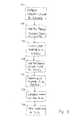
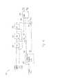
- FIG. 1shows a USB host device on a motherboard of a computer connected to an external USB device through an internal cable and an external cable according to one or more embodiments of the present disclosure.
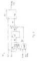
- FIG. 2shows a block diagram of a signal impairment calibration and compensation system of the USB host device of FIG. 1 used to perform calibration of signal impairments introduced by an internal cable connected to the USB device during a calibration phase according to one or more embodiments of the present disclosure.
- FIG. 3shows a flow chart of a method for calibrating a transmit and receive insertion loss through an internal cable using the system of FIG. 2 according to one or more embodiments of the present disclosure.
- FIG. 4shows a block diagram of portions of an impairment compensation module used to compensate the transmit insertion loss of an internal cable when transmitting USB signals through the internal cable according to one or more embodiments of the present disclosure.
- FIG. 5shows a block diagram of portions of an impairment compensation module used to compensate the receive insertion loss of an internal cable when receiving USB signals through the internal cable according to one or more embodiments of the present disclosure.
- FIG. 6shows a flow chart of a method for calibrating a transmit and receive intra-pair skew through an internal cable using the system of FIG. 2 according to one or more embodiments of the present disclosure.
- FIG. 7shows a block diagram of portions of an impairment compensation module used to compensate the transmit intra-pair skew of an internal cable when transmitting USB signals through the internal cable according to one or more embodiments of the present disclosure.
- FIG. 8shows a block diagram of portions of an impairment compensation module used to compensate the receive intra-pair skew of an internal cable when receiving USB signals through the internal cable according to one or more embodiments of the present disclosure.
- Txdata transmit
- Rxdata receive
- FIG. 1shows a USB 3.0 (hereinafter simply USB) host device on a motherboard 102 of a computer connected to an external USB device 134 through an internal cable 106 and an external cable 108 according to one or more embodiments of the present disclosure.
- the motherboard 102contains a USB physical layer device (PHY) 103 which generates Tx data and receives Rx data through a host USB port 104 .
- Full duplex data signals from host USB port 104include a differential pair of transmit signals TxP, TxN and a differential pair of receive signals RxP, RxN.
- Differential signals TxP/TxN, RxP/RxNare carried on twisted pairs of wires through the internal cable 106 that is connected to host USB port 104 on one end and connected to a front panel USB port 114 on a front panel 116 of the computer on the other end.
- the external cable 108carries the differential signals from front panel 116 to the external device 134 .
- USB host device 103 of the computer and external device 134communicate through internal cable 106 and external cable 108 .
- TxP/TxNSignal impairments on TxP/TxN, RxP/RxN are introduced by both internal cable 106 and external cable 108 . These signal impairments may include frequency dependent insertion loss on TxP/TxN, RxP/RxN, and intra-pair skews between differential signals TxP/TxN, and between RxP/RxN. While the USB standard specifies limits on insertion loss and intra-pair skews for TxP/TxN and RxP/RxN through external cable 108 , the limits for internal cable 106 are not as well defined.
- FIG. 2shows a block diagram of a signal impairment calibration and compensation system of the USB host device (e.g., USB PHY 103 ) of FIG. 1 used to perform calibration of signal impairments introduced by an internal cable connected to the USB device during a calibration phase according to one or more embodiments of the present disclosure.
- the USB host devicehas a controller 202 that runs calibration firmware 204 to transmit calibration signals onto the twisted pair carrying TxP/TxN of internal cable 106 .
- the calibration phaseuses a loop back test in which the calibration signals on TxP/TxN are looped back as RxP/RxN at front panel 114 .
- Calibration firmware 204running on controller 202 measures insertion loss by comparing the received calibration signals with the transmitted calibration signals. From the measurement, controller 202 determines the insertion loss attributable to the twisted pair of internal cable 106 carrying TxP/TxN and saves it as Tx insertion loss into a calibration measurement memory 206 . Similarly, controller 202 determines the Rx insertion loss attributable to the twisted pair of internal cable 106 carrying RxP/RxN internal cable 106 and saves it as Rx insertion loss into calibration measurement memory 206 .
- controller 202From the received calibration signals, controller 202 also determines the intra-pair skew introduced by the twisted pair carrying TxP/TxN and saves it as Tx intra-pair skew into calibration measurement memory 206 . Similarly, controller 202 determines the intra-pair skew introduced by the twisted pair carrying RxP/RxN and saves it as Rx intra-pair skew into calibration measurement memory 206 .
- calibration measurement memory 206may be implemented as a non-volatile memory so that the impairment compensation settings are saved even after power to the computer is turned off. The calibration phase may be run during a system characterization step after a new internal cable is connected to the USB host device.
- An impairment compensation module 210reads the impairment compensation settings from calibration measurement memory 206 and applies the settings to TxP/TxN and RxP/RxN. For example, impairment compensation module 210 applies compensation settings for Tx insertion loss and Tx intra-pair skew to transmit data Tx data 214 to generate TxP/TxN. TxP/TxN is thus compensated for the insertion loss and the intra-pair skew introduced by the twisted pair carrying TxP/TxN of internal cable 106 .
- impairment compensation module 210applies compensation settings for Rx insertion loss and Rx intra-pair skew to RxP/RxN to generate received data Rx data 216 .
- RxP/RxNis thus compensated for the insertion loss and the intra-pair skew introduced by the twisted pair carrying RxP/RxN of internal cable 106 .
- FIG. 3shows a flow chart of a method for calibrating Tx and Rx insertion loss introduced by an internal cable using the set up of FIG. 2 according to one or more embodiments of the present disclosure.
- the methodstarts at step 302 , where calibration connector 224 is used to connect the twisted pair carrying TxP/TxN to the twisted pair carrying RxP/RxN as shown in FIG. 2 for looping back TxP to RxP, and TxN to RxN.
- controller 202transmits a low frequency calibration signal of a known amplitude onto the twisted pair carrying TxP/TxN.
- the frequency of the low frequency calibration signalis 2.5 GHz/8.
- the low frequency calibration signalis looped back onto the twisted pair carrying RxP/RxN and its peak amplitude V L is measured by controller 202 in step 306 . Due to the insertion loss introduced by the twisted pairs, the amplitude of the received calibration signal is attenuated from that of the transmitted calibration signal.
- controller 202transmits a high frequency calibration signal with the same amplitude as that of the low frequency calibration signal onto the twisted pair carrying TxP/TxN.
- the frequency of the high frequency calibration signalis 2.5 GHz, or 8 times of the frequency of the low frequency calibration signal.
- the high frequency calibration signalis similarly looped back onto the twisted pair carrying RxP/RxN and its peak amplitude V H is measured by controller 202 in step 310 .
- controller 202calculates the ratio of V H /V L as the combined insertion loss introduced by the two twisted pairs carrying TxP/TxN, RxP/RxN, and by calibration connector 224 .
- the combined insertion lossmay be expressed in dB (decibel) by calculating 10*log(V H /V L ).
- Tx insertion loss and Rx insertion lossrepresent the measured insertion loss for the signal frequency of interest attributable to the twisted pair carrying TxP/TxN and RxP/RxN, respectively.
- the Tx insertion loss and the Rx insertion lossare saved into calibration measurement memory 206 .
- FIG. 4shows a block diagram of portions of an impairment compensation module 210 of FIG. 2 used to compensate the Tx insertion loss of an internal cable 106 when transmitting USB signals through the internal cable according to one or more embodiments of the present disclosure.
- a three-tap FIR (finite impulse response) filteris used for the Tx insertion loss compensation by adjusting the amplitude of TxP/TxN as a function of signal frequency.
- FIR filterswith a different number of taps or other types of filters or adaptive equalizer may be used.
- the flip-flops (F/F) for the three-tap FIR filterare an early tap 408 , a center tap 410 , and a late tap 412 .
- Tx data 214 to be transmitted from the host USB deviceis received by the three-tap FIR filter and is successively clocked through early tap 408 , center tap 410 , and late tap 412 with a clock signal CLK 218 .
- Tx data 214may have already been compensated for Tx intra-pair skew when received as TxDataP and TxDataN for Tx insertion loss compensation.
- TxDataP and TxDataNmay be processed in parallel FIR filters using duplicate tap coefficients but with separate clocks to generate TxP/TxN, respectively.
- Tx data 214may be compensated first for Tx insertion loss and then for Tx intra-pair skew.
- Tx data 214may thus be received as a single-ended signal by a single three-tap FIR filter and then subsequently expanded into TxP/TxN when compensating for Tx intra-pair skew.
- Tx data 214may be compensated for Tx insertion loss and for Tx intra-pair skew in an integrated approach.
- Tx data 214may thus be received as a single-ended signal by two parallel three-tap FIR filters with duplicate tap coefficients. Each of the two parallel three-tap FIR filters is clocked by its own clock adjusted for intra-pair skew to generate TxP/TxN that is compensated for both Tx insertion loss and intra-pair skew.
- the coefficient for center tap 410is set to 1.
- the coefficient for early tap 408is early tap coefficient 404
- the coefficient for late tap 412is late tap coefficient 406 .
- early tap coefficient 404 and late tap coefficient 406are less than 1.
- Early tap coefficient 404 and late tap coefficient 406are stored and read from a Tx insertion loss compensation look up table (LUT) 402 .
- Tx insertion loss saved in calibration measurement memory 206is used as a read address for Tx insertion loss compensation LUT 402 to read out early tap coefficient 404 and late tap coefficient 406 .
- early tap coefficient 404 and late tap coefficient 406represent the FIR coefficients used to compensate TxP/TxN for the measured Tx insertion loss.
- a first multiplier 416multiplies data of early tap 408 with early tap coefficient 404 to generate early tap product 418 .
- a second multiplier 420multiplies data of late tap 412 with late tap coefficient 406 to generate late tap product 422 .
- the tap coefficient for center tap 410is 1. Therefore, no multiplier is necessary for center tap data 424 .
- An adder 426sums early tap product 418 , center tap data 424 , and late tap product 422 to generate TxP/TxN.
- FIG. 5shows a block diagram of portions of an impairment compensation module 210 used to compensate the Rx insertion loss of an internal cable 106 when receiving USB signals through the internal cable according to one or more embodiments of the present disclosure.
- a continuous time linear equalizer 506is used to compensate RxP/RxN for Rx insertion loss.
- Equalization coefficients 504 for continuous time linear equalizer 506are received from a light weight equalization adaptation module 502 .
- Equalization coefficients 504may have a nominal value to boost high frequency signals on RxP/RxN to compensate for the higher Rx insertion loss associated with a higher data rate. This nominal value is based on the Rx insertion loss received from calibration measurement memory 206 and thus compensates for the Rx insertion loss attributable to internal cable 106 .
- continuous time linear equalizer 506may receive equalization coefficients 504 to boost high frequency signals on RxP/RxN by approximately 3-4 dB.
- a high frequency/low frequency energy measurement module 510may be used to measure the energy of high frequency components and the energy of low frequency components of RxP/RxN.
- a ratio of the energies of the two frequency componentsmay be generated as an equalization coefficient adjustment signal 512 for light weight equalization adaptation module 502 to adaptively adjust the nominal value of equalization coefficients 504 .
- equalization coefficients 504may be adaptively adjusted in a simplified manner compared to a full-fledged equalization adaptation algorithm at a cost of decreased performance.
- RxP/RxNmay be compensated for Rx insertion loss first before compensating for Rx intra-pair skew.
- RxDataP/RxDataN from linear equalizer 506would then be compensated for Rx intra-pair skew before bit slicing to generate RxData 216 .
- RxP/RxN as received by linear equalizer 506 for Rx insertion loss compensationmay already have been compensated for Rx intra-pair skew.
- the output of linear equalizer 506 designated as RxDataP/RxDataNmay thus be provided to a slicer to generate RxData 216 .
- FIG. 6shows a flow chart of a method for calibrating Tx and Rx intra-pair skews through an internal cable using the set up of FIG. 2 according to one or more embodiments of the present disclosure.
- the methodstarts at step 602 , where a first type of calibration connector 224 is used to connect the twisted pair carrying TxP/TxN to the twisted pair carrying RxP/RxN as shown in FIG. 2 for looping back TxP to RxP, and TxN to RxN.
- controller 202transmits a skew calibration signal for TxP/TxN.
- the skew calibration signalmay be a pulse or other type of signal that allows the intra-pair skew of the looped back signal to be measured.
- the skew calibration signalis looped back as RxP/RxN and the intra-pair skew M1 between RxP/RxN is measured in step 606 by controller 202 .
- the intra-pair skewmay be measured using multiphase clocks having equally phased offsets as disclosed in U.S. patent application Ser. No. 13/035,331, filed Feb. 25, 2011, entitled “Multiphase Clock Generation and Calibration,” which is incorporated herein by reference in its entirety.
- the signal delay from the transmission of TxP to the reception of RxP by controller 202is D TxP +D RxP .
- the signal delay from the transmission of TxN to the reception of RxN by controller 202is D TxN D RxN .
- M1may be calculated as (D TxP +D RxP ) ⁇ (D TxN +D RxN ).
- a second type of calibration connector 224is used to loop back TxP to RxN, and TxN to RxP.
- controller 202transmits a skew calibration signal for TxP/TxN.
- the skew calibration signalmay be the same as, or may be different from the skew calibration signal transmitted in step 604 .
- the skew calibration signal transmitted on TxPis now looped back as RxN, and the skew calibration signal transmitted on TxN is now looped back as RxP.
- the intra-pair skew M2 between RxP/RxNis measured by control 202 .
- the signal delay from the transmission of TxP to the reception of RxN by controller 202is D TxP +D RxN .
- the signal delay from the transmission of TxN to the reception of RxP by controller 202is D TxN +D RxP ). Therefore, M2 may be calculated as (D TxP +D RxN ) ⁇ (D TxN +D RxP ).
- intra-pair skew between TxP/TxN attributable to the twisted-pair carrying TxP/TxNis calculated by taking the average of M1 and M2:
- intra-pair skew between RxP/RxN attributable to the twisted-pair carrying RxP/RxNis calculated by taking half of the difference between M1 and M2:
- step 616the intra-pair skew D TxP ⁇ D TxN is stored into calibration measurement memory 206 as Tx intra-pair skew.
- the intra-pair skew D RxP ⁇ D RxNis stored into calibration measurement memory 206 as Rx intra-pair skew.
- FIG. 7shows a block diagram of portions of an impairment compensation module 210 used to compensate the Tx intra-pair skew of an internal cable 106 when transmitting USB signals through the internal cable according to one or more embodiments of the present disclosure.
- Tx data 214 to be transmitted from the host USB devicemay be received as differential pair TxDataP and TxDataN.
- TxDataP and TxDataNare individually compensated for Tx intra-pair skew by selectively delaying clocks used to generate TxP/TxN from TxDataP/TxDataN.
- Tx intra-pair skew measured during the calibration phaseindicates that the twisted-pair carrying TxP/TxN TxP delays TxP more than TxN, then a corresponding delay may be introduced onto the clock to delay TxN to offset the delay on TxP.
- TxP clock delay 704 and TxN clock delay 706are stored and read from a Tx skew compensation LUT 702 .
- the Tx intra-pair skew saved in calibration measurement memory 206is used as a read address for Tx skew compensation LUT 702 to read out TxP clock delay 704 and TxN clock delay 706 .
- clock delaysare realized with RC (resistor-capacitor) networks in which varactors, or switch capacitors are used to adjust the clock delays.
- a TxP clock 720is delayed using a RC network of a TxP resistor 710 connected in series with a TxP varactor 708 .
- TxP clock delay 704 from Tx skew compensation LUT 702adjusts the capacitance of TxP varactor 708 to change the RC constant to effect delays on TxP clock 720 .
- a TxN clock 722is delayed using a RC network of a TxN resistor 714 connected in series with a TxN varactor 712 .
- TxN clock delay 706 from Tx skew compensation LUT 702adjusts the capacitance of TxN varactor 712 to change the RC constant to effect delays on TxN clock 722 .
- clock delaysmay alternatively be a network of line delay taps, each tap selectively switched by outputs of Tx skew compensation LUT 702 .
- a TxP F/F 716uses TxP clock 720 to clock in TxDataP.
- a TxN F/F 718uses TxN clock 722 to clock in TxDataN.
- TxP clocked out of TxP F/F 716 and TxN clocked out of TxN F/F 718are skewed with respect to one another to compensate for the Tx intra-pair skew introduced by the twisted pair carrying TxP/TxN.
- TxP/TxNmay subsequently be compensated for Tx insertion loss by providing TxP/TxN to the block diagram of FIG. 4 .
- FIG. 8shows a block diagram of portions of an impairment compensation module 210 used to compensate the Rx intra-pair skew of an internal cable 106 when receiving USB signals through the internal cable according to one or more embodiments of the present disclosure.
- Differential signals RxP and RxNare compensated for intra-pair skew through common mode extraction and filtering.
- a common mode extraction module 806receives RxP/RxN and determines the common mode between them. In one or more embodiments, the common mode may be calculated as an average of RxP and RxN.
- differential signals RxP/RxNmay be compensated first for Rx insertion loss followed by compensating for Rx intra-pair skew. Therefore, RxP/RxN received by FIG. 8 may then be the RxDataP/RxDataN signals from linear equalizer 506 of FIG. 5 that have been compensated for the Rx insertion loss.
- the common mode of a pair of ideal differential signalsis zero. If there is intra-pair skew, the common mode may deviate from zero.
- a common mode error signal 807is generated by a common mode extraction module 806 and filtered by a common mode LPF (low pass filter) 808 to generate a filtered common mode error 809 as an indication of the intra-pair skew.
- common mode LPF 808may be an RC filter.
- Filtered common mode error 809may be substituted for RxN as an input to a bit slicer 814 .
- Bit slicer 814calculates the difference between RxP and filtered common mode error 809 to make a hard decision on Rx data 216 .
- bit slicer 814incurs a 6 dB loss in SNR (signal-to-noise ratio) when using RxP minus filtered common mode error 809 for bit slicing compared to using RxP minus RxN for bit slicing. Therefore, it is desirable to use filtered common mode error 809 for bit slicing only when the intra-pair skew on RxP/RxN is significant.
- Intra-pair skew on RxP/RxNis a combination of intra-pair skews introduced by external cable 108 as well as by internal cable 106 . Because external cable 108 has to be in compliance with limits on signal impairments set by the USB standard, it is likely that the intra-pair skew attributable to internal cable 106 is more than that attributable to external cable 108 . The intra-pair skew attributable to internal cable 106 was measured during the calibration phase and was stored as the Rx intra-pair skew in calibration measurement memory 206 . Therefore, the measured Rx intra-pair skew from internal cable 106 may be a good indicator of the over-all intra-pair skew on RxP/RxN.
- the Rx intra-pair skewis compared with a skew threshold by an Rx comparator 802 .
- the skew thresholdmay be an adjustable threshold set by controller 202 .
- Rx comparator 802generates a select signal 804 based on the comparison. If the Rx intra-pair skew exceeds the skew threshold, the intra-pair skew on RxP/RxN is likely to be significant. Accordingly, select signal 804 is used by multiplexor 810 to select filtered common mode error 809 as a minus input 812 to bit slicer 814 to compensate RxP/RxN for intra-pair skew at a cost of a 6 dB loss in SNR.
- FIG. 8discloses a switchable intra-pair skew compensation approach that bypasses the compensation if the intra-pair skew is not likely to be significant.
- Such componentsmay be implemented with appropriate hardware and/or software to perform the various operations described herein.
- such componentsmay include one or more processors, logic, memory, non-transitory machine readable instructions (e.g., software, firmware, or other instructions stored in a memory or a machine readable medium), and/or other components as may be desired in particular implementations.
- various embodiments provided by the present disclosurecan be implemented using hardware, software, or combinations of hardware and software. Also where applicable, the various hardware components and/or software components set forth herein can be combined into composite components comprising software, hardware, and/or both without departing from the spirit of the present disclosure. Where applicable, the various hardware components and/or software components set forth herein can be separated into sub-components comprising software, hardware, or both without departing from the spirit of the present disclosure. In addition, where applicable, it is contemplated that software components can be implemented as hardware components, and vice-versa.
- Software in accordance with the present disclosurecan be stored on one or more non-transitory machine readable mediums. It is also contemplated that software identified herein can be implemented using one or more general purpose or specific purpose computers and/or computer systems, networked and/or otherwise. Where applicable, the ordering of various steps described herein can be changed, combined into composite steps, and/or separated into sub-steps to provide features described herein.
Landscapes
- Engineering & Computer Science (AREA)
- Power Engineering (AREA)
- Computer Networks & Wireless Communication (AREA)
- Signal Processing (AREA)
- Cable Transmission Systems, Equalization Of Radio And Reduction Of Echo (AREA)
- Dc Digital Transmission (AREA)
Abstract
Description
Claims (20)
Priority Applications (1)
| Application Number | Priority Date | Filing Date | Title |
|---|---|---|---|
| US13/035,710US8935125B1 (en) | 2011-02-25 | 2011-02-25 | Internal cable calibration and compensation |
Applications Claiming Priority (1)
| Application Number | Priority Date | Filing Date | Title |
|---|---|---|---|
| US13/035,710US8935125B1 (en) | 2011-02-25 | 2011-02-25 | Internal cable calibration and compensation |
Publications (1)
| Publication Number | Publication Date |
|---|---|
| US8935125B1true US8935125B1 (en) | 2015-01-13 |
Family
ID=52247840
Family Applications (1)
| Application Number | Title | Priority Date | Filing Date |
|---|---|---|---|
| US13/035,710Active2032-10-26US8935125B1 (en) | 2011-02-25 | 2011-02-25 | Internal cable calibration and compensation |
Country Status (1)
| Country | Link |
|---|---|
| US (1) | US8935125B1 (en) |
Cited By (15)
| Publication number | Priority date | Publication date | Assignee | Title |
|---|---|---|---|---|
| CN105530028A (en)* | 2015-11-26 | 2016-04-27 | 杭州华为数字技术有限公司 | Equalizer configuration method and management module |
| US9461677B1 (en)* | 2015-01-08 | 2016-10-04 | Inphi Corporation | Local phase correction |
| US9491713B2 (en) | 2014-08-06 | 2016-11-08 | U-Blox Ag | Compensator module for a transceiver unit, radio system and method of operating thereof |
| US9887733B2 (en)* | 2014-09-12 | 2018-02-06 | Lattice Semiconductor Corporation | Calibration for echo cancellation in a full duplex communication system |
| WO2021042102A1 (en)* | 2019-08-23 | 2021-03-04 | Microchip Technology Incorporated | Detecting collisions on a network |
| US11074209B2 (en) | 2019-08-23 | 2021-07-27 | Microchip Technology Incorporated | Transceiver and driver architecture with low emission and high interference tolerance |
| US11121782B2 (en) | 2019-08-23 | 2021-09-14 | Microchip Technology Incorporated | Diagnosing cable faults within a network |
| US11171732B2 (en) | 2019-08-23 | 2021-11-09 | Microchip Technology Incorporated | Ethernet interface and related systems methods and devices |
| US11197322B2 (en) | 2019-05-03 | 2021-12-07 | Microchip Technology Incorporated | Emulating collisions in wired local area networks and related systems, methods, and devices |
| JP2022515270A (en)* | 2018-12-25 | 2022-02-17 | 中興通訊股▲ふん▼有限公司 | Connector structure, delay time difference calculation method and equipment |
| US11431468B2 (en) | 2019-08-23 | 2022-08-30 | Microchip Technology Incorporated | Physical layer to link layer interface and related systems, methods and devices |
| US11513577B2 (en) | 2020-03-24 | 2022-11-29 | Microchip Technology Incorporated | Low connection count interface wake source communication according to 10SPE local and remote wake and related systems, methods, and devices |
| US11516855B2 (en) | 2019-08-23 | 2022-11-29 | Microchip Technology Incorporated | Interface for improved media access, and related systems, methods, and devices |
| US11671521B2 (en) | 2019-08-23 | 2023-06-06 | Microchip Technology Incorporated | Ethernet interface and related systems, methods and devices |
| US11670540B2 (en) | 2016-08-11 | 2023-06-06 | Soitec | Substrates including useful layers |
Citations (15)
| Publication number | Priority date | Publication date | Assignee | Title |
|---|---|---|---|---|
| US5673133A (en)* | 1995-04-14 | 1997-09-30 | Nippon Telegraph And Telephone Corporation | Phase synchronization system |
| US20030235253A1 (en)* | 1997-06-20 | 2003-12-25 | Massachusetts Institute Of Technology | Digital transmitter with equalization |
| US20050264299A1 (en)* | 2004-05-28 | 2005-12-01 | Manani Mansukh C | Method and apparatus for measuring insertion loss of a conductor |
| US20060166525A1 (en)* | 2005-01-25 | 2006-07-27 | Fujitsu Component Limited | Evaluation board and cable assembly evaluation method |
| US20070132485A1 (en)* | 2005-12-09 | 2007-06-14 | Elad Alon | Four-wire signaling system |
| US7236108B2 (en)* | 2003-11-04 | 2007-06-26 | Mediatek Inc. | Method and apparatus for data recovery |
| US20080069191A1 (en)* | 2006-09-15 | 2008-03-20 | Dong Yikui Jen | Band-pass high-order analog filter backed hybrid receiver equalization |
| US20080109180A1 (en)* | 2006-11-02 | 2008-05-08 | Redmere Technology Ltd. | System and method for calibrating a high-speed cable |
| US7375532B1 (en)* | 2002-06-07 | 2008-05-20 | Marvell International Ltd. | Cable tester |
| US7426235B1 (en)* | 2004-10-15 | 2008-09-16 | Xilinx, Inc. | Method of adaptive equalization for high-speed NRZ and multi-level signal data communications |
| US20090030635A1 (en)* | 2007-07-25 | 2009-01-29 | Redmere Technology Ld. | Self calibrating cable for a high definition digital video interface |
| US20100283532A1 (en)* | 2006-11-02 | 2010-11-11 | John Martin Horan | Startup circuit and high speed cable using the same |
| US7848404B2 (en)* | 2007-04-05 | 2010-12-07 | Applied Micro Circuits Corporation | Current mode logic multi-tap feed-forward equalizer |
| US20120087405A1 (en)* | 2010-10-12 | 2012-04-12 | Pericom Semiconductor Corp. | Trace Canceller with Equalizer Adjusted for Trace Length Driving Variable-Gain Amplifier with Automatic Gain Control Loop |
| US8179144B1 (en)* | 2002-06-07 | 2012-05-15 | Marvell International Ltd. | Cable tester |
- 2011
- 2011-02-25USUS13/035,710patent/US8935125B1/enactiveActive
Patent Citations (15)
| Publication number | Priority date | Publication date | Assignee | Title |
|---|---|---|---|---|
| US5673133A (en)* | 1995-04-14 | 1997-09-30 | Nippon Telegraph And Telephone Corporation | Phase synchronization system |
| US20030235253A1 (en)* | 1997-06-20 | 2003-12-25 | Massachusetts Institute Of Technology | Digital transmitter with equalization |
| US7375532B1 (en)* | 2002-06-07 | 2008-05-20 | Marvell International Ltd. | Cable tester |
| US8179144B1 (en)* | 2002-06-07 | 2012-05-15 | Marvell International Ltd. | Cable tester |
| US7236108B2 (en)* | 2003-11-04 | 2007-06-26 | Mediatek Inc. | Method and apparatus for data recovery |
| US20050264299A1 (en)* | 2004-05-28 | 2005-12-01 | Manani Mansukh C | Method and apparatus for measuring insertion loss of a conductor |
| US7426235B1 (en)* | 2004-10-15 | 2008-09-16 | Xilinx, Inc. | Method of adaptive equalization for high-speed NRZ and multi-level signal data communications |
| US20060166525A1 (en)* | 2005-01-25 | 2006-07-27 | Fujitsu Component Limited | Evaluation board and cable assembly evaluation method |
| US20070132485A1 (en)* | 2005-12-09 | 2007-06-14 | Elad Alon | Four-wire signaling system |
| US20080069191A1 (en)* | 2006-09-15 | 2008-03-20 | Dong Yikui Jen | Band-pass high-order analog filter backed hybrid receiver equalization |
| US20080109180A1 (en)* | 2006-11-02 | 2008-05-08 | Redmere Technology Ltd. | System and method for calibrating a high-speed cable |
| US20100283532A1 (en)* | 2006-11-02 | 2010-11-11 | John Martin Horan | Startup circuit and high speed cable using the same |
| US7848404B2 (en)* | 2007-04-05 | 2010-12-07 | Applied Micro Circuits Corporation | Current mode logic multi-tap feed-forward equalizer |
| US20090030635A1 (en)* | 2007-07-25 | 2009-01-29 | Redmere Technology Ld. | Self calibrating cable for a high definition digital video interface |
| US20120087405A1 (en)* | 2010-10-12 | 2012-04-12 | Pericom Semiconductor Corp. | Trace Canceller with Equalizer Adjusted for Trace Length Driving Variable-Gain Amplifier with Automatic Gain Control Loop |
Non-Patent Citations (1)
| Title |
|---|
| Ruifeng Sun, "A Low-Power 20-Gb/s Continuous-Time Adaptive Passive Equalizer", 2005, Carnegie Mellon University, pp. 1-71.* |
Cited By (23)
| Publication number | Priority date | Publication date | Assignee | Title |
|---|---|---|---|---|
| US9491713B2 (en) | 2014-08-06 | 2016-11-08 | U-Blox Ag | Compensator module for a transceiver unit, radio system and method of operating thereof |
| US9887733B2 (en)* | 2014-09-12 | 2018-02-06 | Lattice Semiconductor Corporation | Calibration for echo cancellation in a full duplex communication system |
| US9461677B1 (en)* | 2015-01-08 | 2016-10-04 | Inphi Corporation | Local phase correction |
| CN105530028A (en)* | 2015-11-26 | 2016-04-27 | 杭州华为数字技术有限公司 | Equalizer configuration method and management module |
| US11670540B2 (en) | 2016-08-11 | 2023-06-06 | Soitec | Substrates including useful layers |
| JP2022515270A (en)* | 2018-12-25 | 2022-02-17 | 中興通訊股▲ふん▼有限公司 | Connector structure, delay time difference calculation method and equipment |
| JP7498176B2 (en) | 2018-12-25 | 2024-06-11 | 中興通訊股▲ふん▼有限公司 | Connector test fixture, delay time difference calculation method and test device |
| US11995389B2 (en) | 2018-12-25 | 2024-05-28 | Zte Corporation | Connector structure, and skew calculation method and device |
| US11197322B2 (en) | 2019-05-03 | 2021-12-07 | Microchip Technology Incorporated | Emulating collisions in wired local area networks and related systems, methods, and devices |
| US11074209B2 (en) | 2019-08-23 | 2021-07-27 | Microchip Technology Incorporated | Transceiver and driver architecture with low emission and high interference tolerance |
| US11757550B2 (en) | 2019-08-23 | 2023-09-12 | Microchip Technology Incorporated | Ethernet interface and related systems, methods and devices |
| US12323192B2 (en) | 2019-08-23 | 2025-06-03 | Microchip Technology Incorporated | Diagnosing cable faults within a network |
| US11516855B2 (en) | 2019-08-23 | 2022-11-29 | Microchip Technology Incorporated | Interface for improved media access, and related systems, methods, and devices |
| US11665020B2 (en) | 2019-08-23 | 2023-05-30 | Microchip Technology Incorporated | Detecting collisions on a network |
| US11671521B2 (en) | 2019-08-23 | 2023-06-06 | Microchip Technology Incorporated | Ethernet interface and related systems, methods and devices |
| US11171732B2 (en) | 2019-08-23 | 2021-11-09 | Microchip Technology Incorporated | Ethernet interface and related systems methods and devices |
| US11431468B2 (en) | 2019-08-23 | 2022-08-30 | Microchip Technology Incorporated | Physical layer to link layer interface and related systems, methods and devices |
| US11121782B2 (en) | 2019-08-23 | 2021-09-14 | Microchip Technology Incorporated | Diagnosing cable faults within a network |
| WO2021042102A1 (en)* | 2019-08-23 | 2021-03-04 | Microchip Technology Incorporated | Detecting collisions on a network |
| US12256443B2 (en) | 2019-08-23 | 2025-03-18 | Microchip Technology Incorporated | Changing carrier sense signal generated by a reconciliation sublayer of a physical layer that may cause unintended signaling at a reduced media independent interface (RMII) |
| US12137156B2 (en) | 2019-08-23 | 2024-11-05 | Microchip Technology Incorporated | Physical layer to link layer interface and related systems, methods and devices |
| US12093103B2 (en) | 2020-03-24 | 2024-09-17 | Microchip Technology Incorporated | Wake source communication according to 10SPE local and remote wake and related systems, methods, and devices |
| US11513577B2 (en) | 2020-03-24 | 2022-11-29 | Microchip Technology Incorporated | Low connection count interface wake source communication according to 10SPE local and remote wake and related systems, methods, and devices |
Similar Documents
| Publication | Publication Date | Title |
|---|---|---|
| US8935125B1 (en) | Internal cable calibration and compensation | |
| US20050201454A1 (en) | System and method for automatically calibrating two-tap and multi-tap equalization for a communications link | |
| US9960855B2 (en) | High-speed optical communications system | |
| US7447260B2 (en) | Equalizer, equalization method, and transmitter | |
| CN107832246B (en) | Semiconductor device with a semiconductor device having a plurality of semiconductor chips | |
| US11228468B2 (en) | Serdes equalization for short, reflective channels | |
| EP2638673B1 (en) | Adjustable finite impulse response transmitter | |
| WO2008026289A1 (en) | Data transmitting circuit and transmitting method | |
| US20100118930A1 (en) | Signal transmission apparatus and method | |
| KR20210027518A (en) | Method for measuring and correcting multiwire skew | |
| US20210014087A1 (en) | Receiver with selectable digital equalization filter options | |
| US8428111B2 (en) | Crosstalk emission management | |
| US7590176B2 (en) | Partial response transmission system and equalizing circuit thereof | |
| US20170346663A1 (en) | Transmission apparatus | |
| US8737461B2 (en) | Receiving equalization device in communication system and receiving equalization method | |
| KR102458308B1 (en) | Transmitting device/Receiving device with relaxed impedance matching | |
| US11063628B2 (en) | Communication device capable of echo cancellation | |
| CN101662432B (en) | Method, system and device for transmission | |
| US20120287345A1 (en) | System and Method for Automatically Tuning Video Signals | |
| US8938771B2 (en) | Network receiver and control method thereof | |
| US7460602B2 (en) | Method for performing high speed serial link output stage having self adaptation for various impairments | |
| JP2008060768A (en) | Termination resistance adjustment method and termination resistance adjustment circuit | |
| Yoo et al. | An adaptation method for FIR pre-emphasis filter on backplane channel |
Legal Events
| Date | Code | Title | Description |
|---|---|---|---|
| AS | Assignment | Owner name:SMSC HOLDINGS S.A.R.L., LUXEMBOURG Free format text:ASSIGNMENT OF ASSIGNORS INTEREST;ASSIGNORS:FU, WEI;THOMAS, CHRISTOPHER;REEL/FRAME:025868/0240 Effective date:20110225 | |
| AS | Assignment | Owner name:SMSC HOLDINGS S.A.R.L., LUXEMBOURG Free format text:ASSIGNMENT OF ASSIGNORS INTEREST;ASSIGNORS:FU, WEI;THOMAS, CHRISTOPHER;SIGNING DATES FROM 20110224 TO 20110225;REEL/FRAME:029776/0494 | |
| STCF | Information on status: patent grant | Free format text:PATENTED CASE | |
| MAFP | Maintenance fee payment | Free format text:PAYMENT OF MAINTENANCE FEE, 4TH YEAR, LARGE ENTITY (ORIGINAL EVENT CODE: M1551) Year of fee payment:4 | |
| AS | Assignment | Owner name:JPMORGAN CHASE BANK, N.A., AS ADMINISTRATIVE AGENT, DELAWARE Free format text:SECURITY INTEREST;ASSIGNORS:MICROCHIP TECHNOLOGY INC.;SILICON STORAGE TECHNOLOGY, INC.;ATMEL CORPORATION;AND OTHERS;REEL/FRAME:053311/0305 Effective date:20200327 | |
| AS | Assignment | Owner name:SILICON STORAGE TECHNOLOGY, INC., ARIZONA Free format text:RELEASE BY SECURED PARTY;ASSIGNOR:JPMORGAN CHASE BANK, N.A, AS ADMINISTRATIVE AGENT;REEL/FRAME:053466/0011 Effective date:20200529 Owner name:MICROSEMI CORPORATION, CALIFORNIA Free format text:RELEASE BY SECURED PARTY;ASSIGNOR:JPMORGAN CHASE BANK, N.A, AS ADMINISTRATIVE AGENT;REEL/FRAME:053466/0011 Effective date:20200529 Owner name:MICROSEMI STORAGE SOLUTIONS, INC., ARIZONA Free format text:RELEASE BY SECURED PARTY;ASSIGNOR:JPMORGAN CHASE BANK, N.A, AS ADMINISTRATIVE AGENT;REEL/FRAME:053466/0011 Effective date:20200529 Owner name:ATMEL CORPORATION, ARIZONA Free format text:RELEASE BY SECURED PARTY;ASSIGNOR:JPMORGAN CHASE BANK, N.A, AS ADMINISTRATIVE AGENT;REEL/FRAME:053466/0011 Effective date:20200529 Owner name:MICROCHIP TECHNOLOGY INC., ARIZONA Free format text:RELEASE BY SECURED PARTY;ASSIGNOR:JPMORGAN CHASE BANK, N.A, AS ADMINISTRATIVE AGENT;REEL/FRAME:053466/0011 Effective date:20200529 | |
| AS | Assignment | Owner name:WELLS FARGO BANK, NATIONAL ASSOCIATION, MINNESOTA Free format text:SECURITY INTEREST;ASSIGNORS:MICROCHIP TECHNOLOGY INC.;SILICON STORAGE TECHNOLOGY, INC.;ATMEL CORPORATION;AND OTHERS;REEL/FRAME:053468/0705 Effective date:20200529 | |
| AS | Assignment | Owner name:WELLS FARGO BANK, NATIONAL ASSOCIATION, AS COLLATERAL AGENT, MINNESOTA Free format text:SECURITY INTEREST;ASSIGNORS:MICROCHIP TECHNOLOGY INCORPORATED;SILICON STORAGE TECHNOLOGY, INC.;ATMEL CORPORATION;AND OTHERS;REEL/FRAME:055671/0612 Effective date:20201217 | |
| AS | Assignment | Owner name:WELLS FARGO BANK, NATIONAL ASSOCIATION, AS NOTES COLLATERAL AGENT, MINNESOTA Free format text:SECURITY INTEREST;ASSIGNORS:MICROCHIP TECHNOLOGY INCORPORATED;SILICON STORAGE TECHNOLOGY, INC.;ATMEL CORPORATION;AND OTHERS;REEL/FRAME:057935/0474 Effective date:20210528 | |
| AS | Assignment | Owner name:MICROSEMI STORAGE SOLUTIONS, INC., ARIZONA Free format text:RELEASE BY SECURED PARTY;ASSIGNOR:WELLS FARGO BANK, NATIONAL ASSOCIATION, AS NOTES COLLATERAL AGENT;REEL/FRAME:059863/0400 Effective date:20220228 Owner name:MICROSEMI CORPORATION, ARIZONA Free format text:RELEASE BY SECURED PARTY;ASSIGNOR:WELLS FARGO BANK, NATIONAL ASSOCIATION, AS NOTES COLLATERAL AGENT;REEL/FRAME:059863/0400 Effective date:20220228 Owner name:ATMEL CORPORATION, ARIZONA Free format text:RELEASE BY SECURED PARTY;ASSIGNOR:WELLS FARGO BANK, NATIONAL ASSOCIATION, AS NOTES COLLATERAL AGENT;REEL/FRAME:059863/0400 Effective date:20220228 Owner name:SILICON STORAGE TECHNOLOGY, INC., ARIZONA Free format text:RELEASE BY SECURED PARTY;ASSIGNOR:WELLS FARGO BANK, NATIONAL ASSOCIATION, AS NOTES COLLATERAL AGENT;REEL/FRAME:059863/0400 Effective date:20220228 Owner name:MICROCHIP TECHNOLOGY INCORPORATED, ARIZONA Free format text:RELEASE BY SECURED PARTY;ASSIGNOR:WELLS FARGO BANK, NATIONAL ASSOCIATION, AS NOTES COLLATERAL AGENT;REEL/FRAME:059863/0400 Effective date:20220228 | |
| AS | Assignment | Owner name:MICROSEMI STORAGE SOLUTIONS, INC., ARIZONA Free format text:RELEASE BY SECURED PARTY;ASSIGNOR:WELLS FARGO BANK, NATIONAL ASSOCIATION, AS NOTES COLLATERAL AGENT;REEL/FRAME:059363/0001 Effective date:20220228 Owner name:MICROSEMI CORPORATION, ARIZONA Free format text:RELEASE BY SECURED PARTY;ASSIGNOR:WELLS FARGO BANK, NATIONAL ASSOCIATION, AS NOTES COLLATERAL AGENT;REEL/FRAME:059363/0001 Effective date:20220228 Owner name:ATMEL CORPORATION, ARIZONA Free format text:RELEASE BY SECURED PARTY;ASSIGNOR:WELLS FARGO BANK, NATIONAL ASSOCIATION, AS NOTES COLLATERAL AGENT;REEL/FRAME:059363/0001 Effective date:20220228 Owner name:SILICON STORAGE TECHNOLOGY, INC., ARIZONA Free format text:RELEASE BY SECURED PARTY;ASSIGNOR:WELLS FARGO BANK, NATIONAL ASSOCIATION, AS NOTES COLLATERAL AGENT;REEL/FRAME:059363/0001 Effective date:20220228 Owner name:MICROCHIP TECHNOLOGY INCORPORATED, ARIZONA Free format text:RELEASE BY SECURED PARTY;ASSIGNOR:WELLS FARGO BANK, NATIONAL ASSOCIATION, AS NOTES COLLATERAL AGENT;REEL/FRAME:059363/0001 Effective date:20220228 | |
| AS | Assignment | Owner name:MICROSEMI STORAGE SOLUTIONS, INC., ARIZONA Free format text:RELEASE BY SECURED PARTY;ASSIGNOR:WELLS FARGO BANK, NATIONAL ASSOCIATION, AS NOTES COLLATERAL AGENT;REEL/FRAME:060894/0437 Effective date:20220228 Owner name:MICROSEMI CORPORATION, ARIZONA Free format text:RELEASE BY SECURED PARTY;ASSIGNOR:WELLS FARGO BANK, NATIONAL ASSOCIATION, AS NOTES COLLATERAL AGENT;REEL/FRAME:060894/0437 Effective date:20220228 Owner name:ATMEL CORPORATION, ARIZONA Free format text:RELEASE BY SECURED PARTY;ASSIGNOR:WELLS FARGO BANK, NATIONAL ASSOCIATION, AS NOTES COLLATERAL AGENT;REEL/FRAME:060894/0437 Effective date:20220228 Owner name:SILICON STORAGE TECHNOLOGY, INC., ARIZONA Free format text:RELEASE BY SECURED PARTY;ASSIGNOR:WELLS FARGO BANK, NATIONAL ASSOCIATION, AS NOTES COLLATERAL AGENT;REEL/FRAME:060894/0437 Effective date:20220228 Owner name:MICROCHIP TECHNOLOGY INCORPORATED, ARIZONA Free format text:RELEASE BY SECURED PARTY;ASSIGNOR:WELLS FARGO BANK, NATIONAL ASSOCIATION, AS NOTES COLLATERAL AGENT;REEL/FRAME:060894/0437 Effective date:20220228 | |
| MAFP | Maintenance fee payment | Free format text:PAYMENT OF MAINTENANCE FEE, 8TH YEAR, LARGE ENTITY (ORIGINAL EVENT CODE: M1552); ENTITY STATUS OF PATENT OWNER: LARGE ENTITY Year of fee payment:8 |