US8933520B1 - Conductive routings in integrated circuits using under bump metallization - Google Patents
Conductive routings in integrated circuits using under bump metallizationDownload PDFInfo
- Publication number
- US8933520B1 US8933520B1US14/194,414US201414194414AUS8933520B1US 8933520 B1US8933520 B1US 8933520B1US 201414194414 AUS201414194414 AUS 201414194414AUS 8933520 B1US8933520 B1US 8933520B1
- Authority
- US
- United States
- Prior art keywords
- conductive
- region
- layer
- area
- electrodes
- Prior art date
- Legal status (The legal status is an assumption and is not a legal conclusion. Google has not performed a legal analysis and makes no representation as to the accuracy of the status listed.)
- Active
Links
- 238000001465metallisationMethods0.000titleclaimsabstractdescription33
- 239000000758substrateSubstances0.000claimsdescription37
- 238000002161passivationMethods0.000claimsdescription5
- 239000010410layerSubstances0.000description291
- 229910052751metalInorganic materials0.000description73
- 239000002184metalSubstances0.000description73
- 238000002955isolationMethods0.000description30
- 229910000679solderInorganic materials0.000description15
- 230000008878couplingEffects0.000description13
- 238000010168coupling processMethods0.000description13
- 238000005859coupling reactionMethods0.000description13
- RYGMFSIKBFXOCR-UHFFFAOYSA-NCopperChemical compound[Cu]RYGMFSIKBFXOCR-UHFFFAOYSA-N0.000description12
- 229910052802copperInorganic materials0.000description12
- 239000010949copperSubstances0.000description12
- 238000009413insulationMethods0.000description6
- 239000004020conductorSubstances0.000description5
- 229910052782aluminiumInorganic materials0.000description4
- XAGFODPZIPBFFR-UHFFFAOYSA-NaluminiumChemical compound[Al]XAGFODPZIPBFFR-UHFFFAOYSA-N0.000description4
- 238000010586diagramMethods0.000description4
- 239000004065semiconductorSubstances0.000description4
- VYPSYNLAJGMNEJ-UHFFFAOYSA-NSilicium dioxideChemical compoundO=[Si]=OVYPSYNLAJGMNEJ-UHFFFAOYSA-N0.000description3
- XUIMIQQOPSSXEZ-UHFFFAOYSA-NSiliconChemical compound[Si]XUIMIQQOPSSXEZ-UHFFFAOYSA-N0.000description3
- RTAQQCXQSZGOHL-UHFFFAOYSA-NTitaniumChemical compound[Ti]RTAQQCXQSZGOHL-UHFFFAOYSA-N0.000description3
- 239000003990capacitorSubstances0.000description3
- 239000012212insulatorSubstances0.000description3
- 229910052710siliconInorganic materials0.000description3
- 239000010703siliconSubstances0.000description3
- 239000010936titaniumSubstances0.000description3
- 229910052719titaniumInorganic materials0.000description3
- 229910000756V alloyInorganic materials0.000description2
- -1e.g.Substances0.000description2
- 230000004048modificationEffects0.000description2
- 238000012986modificationMethods0.000description2
- HBVFXTAPOLSOPB-UHFFFAOYSA-Nnickel vanadiumChemical compound[V].[Ni]HBVFXTAPOLSOPB-UHFFFAOYSA-N0.000description2
- 238000004806packaging method and processMethods0.000description2
- 229910021420polycrystalline siliconInorganic materials0.000description2
- 229920005591polysiliconPolymers0.000description2
- 239000002344surface layerSubstances0.000description2
- 238000003491arrayMethods0.000description1
- 230000004888barrier functionEffects0.000description1
- 230000015572biosynthetic processEffects0.000description1
- 230000001276controlling effectEffects0.000description1
- 238000009792diffusion processMethods0.000description1
- 238000001914filtrationMethods0.000description1
- 239000000463materialSubstances0.000description1
- 150000004767nitridesChemical class0.000description1
- 230000002093peripheral effectEffects0.000description1
- 238000007747platingMethods0.000description1
- 230000001105regulatory effectEffects0.000description1
- 235000012239silicon dioxideNutrition0.000description1
- 239000000377silicon dioxideSubstances0.000description1
- 229910052814silicon oxideInorganic materials0.000description1
- 238000004544sputter depositionMethods0.000description1
Images


Classifications
- H—ELECTRICITY
- H01—ELECTRIC ELEMENTS
- H01L—SEMICONDUCTOR DEVICES NOT COVERED BY CLASS H10
- H01L23/00—Details of semiconductor or other solid state devices
- H01L23/52—Arrangements for conducting electric current within the device in operation from one component to another, i.e. interconnections, e.g. wires, lead frames
- H01L23/522—Arrangements for conducting electric current within the device in operation from one component to another, i.e. interconnections, e.g. wires, lead frames including external interconnections consisting of a multilayer structure of conductive and insulating layers inseparably formed on the semiconductor body
- H01L23/5226—Via connections in a multilevel interconnection structure
- H—ELECTRICITY
- H01—ELECTRIC ELEMENTS
- H01L—SEMICONDUCTOR DEVICES NOT COVERED BY CLASS H10
- H01L23/00—Details of semiconductor or other solid state devices
- H01L23/48—Arrangements for conducting electric current to or from the solid state body in operation, e.g. leads, terminal arrangements ; Selection of materials therefor
- H01L23/482—Arrangements for conducting electric current to or from the solid state body in operation, e.g. leads, terminal arrangements ; Selection of materials therefor consisting of lead-in layers inseparably applied to the semiconductor body (electrodes)
- H01L23/4824—Pads with extended contours, e.g. grid structure, branch structure, finger structure
- H—ELECTRICITY
- H01—ELECTRIC ELEMENTS
- H01L—SEMICONDUCTOR DEVICES NOT COVERED BY CLASS H10
- H01L23/00—Details of semiconductor or other solid state devices
- H01L23/52—Arrangements for conducting electric current within the device in operation from one component to another, i.e. interconnections, e.g. wires, lead frames
- H01L23/522—Arrangements for conducting electric current within the device in operation from one component to another, i.e. interconnections, e.g. wires, lead frames including external interconnections consisting of a multilayer structure of conductive and insulating layers inseparably formed on the semiconductor body
- H—ELECTRICITY
- H01—ELECTRIC ELEMENTS
- H01L—SEMICONDUCTOR DEVICES NOT COVERED BY CLASS H10
- H01L2224/00—Indexing scheme for arrangements for connecting or disconnecting semiconductor or solid-state bodies and methods related thereto as covered by H01L24/00
- H01L2224/01—Means for bonding being attached to, or being formed on, the surface to be connected, e.g. chip-to-package, die-attach, "first-level" interconnects; Manufacturing methods related thereto
- H01L2224/02—Bonding areas; Manufacturing methods related thereto
- H01L2224/04—Structure, shape, material or disposition of the bonding areas prior to the connecting process
- H01L2224/0401—Bonding areas specifically adapted for bump connectors, e.g. under bump metallisation [UBM]
- H—ELECTRICITY
- H01—ELECTRIC ELEMENTS
- H01L—SEMICONDUCTOR DEVICES NOT COVERED BY CLASS H10
- H01L2224/00—Indexing scheme for arrangements for connecting or disconnecting semiconductor or solid-state bodies and methods related thereto as covered by H01L24/00
- H01L2224/01—Means for bonding being attached to, or being formed on, the surface to be connected, e.g. chip-to-package, die-attach, "first-level" interconnects; Manufacturing methods related thereto
- H01L2224/02—Bonding areas; Manufacturing methods related thereto
- H01L2224/04—Structure, shape, material or disposition of the bonding areas prior to the connecting process
- H01L2224/05—Structure, shape, material or disposition of the bonding areas prior to the connecting process of an individual bonding area
- H01L2224/0554—External layer
- H01L2224/05599—Material
- H01L2224/056—Material with a principal constituent of the material being a metal or a metalloid, e.g. boron [B], silicon [Si], germanium [Ge], arsenic [As], antimony [Sb], tellurium [Te] and polonium [Po], and alloys thereof
- H01L2224/05617—Material with a principal constituent of the material being a metal or a metalloid, e.g. boron [B], silicon [Si], germanium [Ge], arsenic [As], antimony [Sb], tellurium [Te] and polonium [Po], and alloys thereof the principal constituent melting at a temperature of greater than or equal to 400°C and less than 950°C
- H01L2224/05624—Aluminium [Al] as principal constituent
- H—ELECTRICITY
- H01—ELECTRIC ELEMENTS
- H01L—SEMICONDUCTOR DEVICES NOT COVERED BY CLASS H10
- H01L2224/00—Indexing scheme for arrangements for connecting or disconnecting semiconductor or solid-state bodies and methods related thereto as covered by H01L24/00
- H01L2224/01—Means for bonding being attached to, or being formed on, the surface to be connected, e.g. chip-to-package, die-attach, "first-level" interconnects; Manufacturing methods related thereto
- H01L2224/02—Bonding areas; Manufacturing methods related thereto
- H01L2224/04—Structure, shape, material or disposition of the bonding areas prior to the connecting process
- H01L2224/05—Structure, shape, material or disposition of the bonding areas prior to the connecting process of an individual bonding area
- H01L2224/0554—External layer
- H01L2224/05599—Material
- H01L2224/056—Material with a principal constituent of the material being a metal or a metalloid, e.g. boron [B], silicon [Si], germanium [Ge], arsenic [As], antimony [Sb], tellurium [Te] and polonium [Po], and alloys thereof
- H01L2224/05638—Material with a principal constituent of the material being a metal or a metalloid, e.g. boron [B], silicon [Si], germanium [Ge], arsenic [As], antimony [Sb], tellurium [Te] and polonium [Po], and alloys thereof the principal constituent melting at a temperature of greater than or equal to 950°C and less than 1550°C
- H01L2224/05647—Copper [Cu] as principal constituent
- H—ELECTRICITY
- H01—ELECTRIC ELEMENTS
- H01L—SEMICONDUCTOR DEVICES NOT COVERED BY CLASS H10
- H01L2224/00—Indexing scheme for arrangements for connecting or disconnecting semiconductor or solid-state bodies and methods related thereto as covered by H01L24/00
- H01L2224/01—Means for bonding being attached to, or being formed on, the surface to be connected, e.g. chip-to-package, die-attach, "first-level" interconnects; Manufacturing methods related thereto
- H01L2224/10—Bump connectors; Manufacturing methods related thereto
- H01L2224/12—Structure, shape, material or disposition of the bump connectors prior to the connecting process
- H01L2224/13—Structure, shape, material or disposition of the bump connectors prior to the connecting process of an individual bump connector
- H01L2224/13001—Core members of the bump connector
- H01L2224/13099—Material
- H01L2224/131—Material with a principal constituent of the material being a metal or a metalloid, e.g. boron [B], silicon [Si], germanium [Ge], arsenic [As], antimony [Sb], tellurium [Te] and polonium [Po], and alloys thereof
- H—ELECTRICITY
- H01—ELECTRIC ELEMENTS
- H01L—SEMICONDUCTOR DEVICES NOT COVERED BY CLASS H10
- H01L23/00—Details of semiconductor or other solid state devices
- H01L23/52—Arrangements for conducting electric current within the device in operation from one component to another, i.e. interconnections, e.g. wires, lead frames
- H01L23/522—Arrangements for conducting electric current within the device in operation from one component to another, i.e. interconnections, e.g. wires, lead frames including external interconnections consisting of a multilayer structure of conductive and insulating layers inseparably formed on the semiconductor body
- H01L23/532—Arrangements for conducting electric current within the device in operation from one component to another, i.e. interconnections, e.g. wires, lead frames including external interconnections consisting of a multilayer structure of conductive and insulating layers inseparably formed on the semiconductor body characterised by the materials
- H01L23/53204—Conductive materials
- H01L23/53209—Conductive materials based on metals, e.g. alloys, metal silicides
- H01L23/53228—Conductive materials based on metals, e.g. alloys, metal silicides the principal metal being copper
- H01L23/53238—Additional layers associated with copper layers, e.g. adhesion, barrier, cladding layers
- H—ELECTRICITY
- H01—ELECTRIC ELEMENTS
- H01L—SEMICONDUCTOR DEVICES NOT COVERED BY CLASS H10
- H01L24/00—Arrangements for connecting or disconnecting semiconductor or solid-state bodies; Methods or apparatus related thereto
- H01L24/01—Means for bonding being attached to, or being formed on, the surface to be connected, e.g. chip-to-package, die-attach, "first-level" interconnects; Manufacturing methods related thereto
- H01L24/02—Bonding areas ; Manufacturing methods related thereto
- H01L24/04—Structure, shape, material or disposition of the bonding areas prior to the connecting process
- H01L24/05—Structure, shape, material or disposition of the bonding areas prior to the connecting process of an individual bonding area
- H—ELECTRICITY
- H01—ELECTRIC ELEMENTS
- H01L—SEMICONDUCTOR DEVICES NOT COVERED BY CLASS H10
- H01L24/00—Arrangements for connecting or disconnecting semiconductor or solid-state bodies; Methods or apparatus related thereto
- H01L24/01—Means for bonding being attached to, or being formed on, the surface to be connected, e.g. chip-to-package, die-attach, "first-level" interconnects; Manufacturing methods related thereto
- H01L24/10—Bump connectors ; Manufacturing methods related thereto
- H01L24/12—Structure, shape, material or disposition of the bump connectors prior to the connecting process
- H01L24/13—Structure, shape, material or disposition of the bump connectors prior to the connecting process of an individual bump connector
- H—ELECTRICITY
- H01—ELECTRIC ELEMENTS
- H01L—SEMICONDUCTOR DEVICES NOT COVERED BY CLASS H10
- H01L2924/00—Indexing scheme for arrangements or methods for connecting or disconnecting semiconductor or solid-state bodies as covered by H01L24/00
- H01L2924/0001—Technical content checked by a classifier
- H01L2924/00014—Technical content checked by a classifier the subject-matter covered by the group, the symbol of which is combined with the symbol of this group, being disclosed without further technical details
- H—ELECTRICITY
- H01—ELECTRIC ELEMENTS
- H01L—SEMICONDUCTOR DEVICES NOT COVERED BY CLASS H10
- H01L2924/00—Indexing scheme for arrangements or methods for connecting or disconnecting semiconductor or solid-state bodies as covered by H01L24/00
- H01L2924/10—Details of semiconductor or other solid state devices to be connected
- H01L2924/11—Device type
- H01L2924/14—Integrated circuits
Definitions
- the present inventionrelates generally to conductive routings in integrated circuits, and in one aspect, to conductive routings in integrated circuits used as power switches.
- Integrated circuitswhich generally refer to electronic circuits formed on a silicon or other semiconductor substrate, have widespread application in modern electronic systems.
- An IC chipmay contain circuit devices, such as transistors, and electrical interconnects to electrically couple the circuit devices.
- An outer surface of the IC chipmay also contain conductive pads for providing electrical coupling of the chip to external devices, such as voltage sources and control circuits.
- electrical connection between the transistors in the semiconductive substrate and the conductive padsis accomplished through the use of multiple conductive layers that are formed over the semiconducting substrate of the integrated circuit chip but below an insulative layer that supports the conductive pads (an aperture in the insulative layer can provide electrical coupling of the contact pad to the uppermost conductive layer).
- an integrated circuit chipmay have metal lines and vias that electrically couple the source and drain regions of the transistors to the conducting pads of the integrated circuit chip.
- Voltage regulatorssuch as DC to DC converters, are used to provide stable voltage sources for electronic systems.
- Switching voltage regulatorsare known to be an efficient type of DC to DC converter.
- Such voltage regulatorstypically include a power switch to generate a rectangular-wave voltage that is filtered to provide the output DC voltage.
- the power switchwas fabricated as an integrated circuit chip with wire bond packaging. More recently, the power switch has been fabricated as an integrated circuit chip with flip-chip packaging (in which solder bumps are placed on the top surface of the chip, and the chip is mounted upside down with the solder bumps connected directly to a printed circuit board, interposer, or to a package).
- an integrated circuit structureincludes a first conductive layer and an under bump metallization layer over the first conductive layer.
- the first conductive layerhas a first conductive region and a second conductive region electrically isolated from the first conductive region.
- the under bump metallization layerhas a first conductive area and a second conductive area electrically isolated from the first conductive area, the first conductive area substantially located over the first conductive region and the second conductive area substantially located over the second conductive region.
- At least one of the first conductive area or the first conductive regionincludes a first protrusion extending toward the second conductive area or second conductive region, respectively.
- Conductive viasconnect the first conductive region to the second conductive area and connect the second conductive region to the first conductive area, and the conductive vias include at least one via connected to the first protrusion.
- the first conductive areamay include the first protrusion extending toward the second conductive area.
- the first conductive regionmay include a second protrusion extending toward the second conductive region, and the conductive vias may include at least one via connected to the second protrusion.
- the first conductive regionmay include the first protrusion extending toward the second conductive region.
- a first flip-chip interconnectmay be on the first conductive area of the under bump metallization layer, and a second flip-chip interconnect may be on the second conductive area of the under bump metallization layer.
- the first flip-chip interconnect and second flip-chip interconnectmay be solder bumps, solder balls, copper pillars or stud bumps.
- the first conductive regionmay have a plurality of first protrusions extending toward the second conductive region, and the second conductive region may have a plurality of second protrusions extending toward the first conductive region.
- the first conductive areamay have a plurality of third protrusions extending toward the second conductive area, and the second conductive area may have a plurality of fourth protrusions extending toward the first conductive area.
- a plurality of first conductive viasmay connect the plurality of first protrusions to the plurality of fourth protrusions, and a plurality of second conductive vias may connect the plurality of second protrusions to the plurality of third protrusions.
- the first conductive areamay have a plurality of first protrusions extending toward the second conductive area, and the second conductive area may have a plurality of second protrusions extending toward the first conductive area.
- the under bump metallizationmay include a contact layer to contact a portion of the first conductive layer and an outer layer.
- An intermediate layermay be between the contact layer and the outer layer.
- the intermediate layermay include a diffusion-blocking material.
- the contact layermay include aluminum, the intermediate layer may include a nickel vanadium alloy, and the outer layer may include copper.
- the contact layermay be titanium and the outer layer may be copper.
- the outer layermay be a metal layer, e.g., copper, having a thickness greater than 6 microns.
- the integrated circuit structuremay further comprise a substrate under the first conductive layer.
- the substratemay have a first distributed transistor with a first plurality of doped source regions and a first plurality of doped drain regions, and the first conductive region and the second conductive area may be electrically coupled to the first plurality of doped source regions and the second conductive region and the first conductive area may be electrically coupled to the first plurality of doped drain regions.
- the first plurality of doped source regions and the first plurality of doped drain regionsmay be are arranged in an alternating pattern in the substrate.
- the substratemay have a second distributed transistor with a second plurality of doped source regions and a second plurality of doped drain regions arranged in an alternating pattern in the substrate.
- the first conductive layermay have a third conductive region and a fourth conductive region electrically isolated from the third conductive region.
- the under bump metallization layermay have a third conductive area and a fourth conductive area electrically isolated from the third conductive area, the third conductive area substantially located over the third conductive region and the second conductive area substantially located over the fourth conductive region.
- At least one of the third conductive area or the third conductive regionmay include a second protrusion extending toward the fourth conductive area or fourth conductive region, respectively.
- the conductive viasmay connect the third conductive region to the fourth conductive area and connect the fourth conductive region to the third conductive area.
- the conductive viasmay include at least one via connected to the second protrusion.
- the third conductive region and the fourth conductivemay be electrically coupled to the second plurality of doped source regions and the fourth conductive region and the third conductive area electrically coupled to the second plurality of doped drain regions.
- the first conductive areamay be electrically coupled to the third conductive area.
- the first conductive areamay be electrically coupled to the fourth conductive area.
- Thee second conductive areamay be electrically coupled to the fourth conductive area.
- a second conductive layermay be between the first conductive layer and the substrate.
- the second conductive layermay include a plurality of first conductive portions and a plurality of second conductive portions disposed below the first conductive region, and may include plurality of third conductive portions and a plurality of fourth conductive portions disposed below the first conductive region.
- a third plurality of viasmay connect the first conductive region to the plurality of first conductive portions, and a fourth plurality of vias may connect the second conductive region to the plurality of third conductive portions.
- a fifth plurality of viasmay connect the first conductive area to the plurality of second conductive portions, and a sixth plurality of vias may connect the second conductive area to the plurality of fourth conductive portions.
- a first flip-chip interconnectmay be on the first conductive area of the under bump metallization layer
- a second flip-chip interconnectmay be on the second conductive area of the under bump metallization layer
- a third flip-chip interconnectmay be on the third conductive area of the under bump metallization layer
- a fourth flip-chip interconnectmay be on the fourth conductive area of the under bump metallization layer.
- an integrated circuit structurein another aspect, includes a first conductive layer and a second conductive layer over the first conductive layer.
- the first conductive layerhas a first conductive region and a second conductive region electrically isolated from the first conductive region.
- the second conductive layerhas a first conductive area and a second conductive area electrically isolated from the first conductive area, the first conductive area substantially located over the first conductive region and the second conductive area substantially located over the second conductive region. Only one of the first conductive area or the first conductive region includes a first protrusion extending toward the second conductive area or second conductive region, respectively.
- Conductive viasconnect the first conductive region to the second conductive area and connect the second conductive region to the first conductive area.
- the conductive viasinclude at least one via connected to the first protrusion.
- the first conductive areamay include the first protrusion extending toward the second conductive area.
- the first conductive regionmay include the first protrusion extending toward the second conductive region.
- the first conductive regionmay have a plurality of first protrusions extending toward the second conductive region, and the second conductive region may have a plurality of second protrusions extending toward the first conductive region.
- the first conductive areamay have a plurality of third protrusions extending toward the second conductive area, and the second conductive area may have a plurality of fourth protrusions extending toward the first conductive area.
- a plurality of first conductive viasmay connect the plurality of first protrusions to the plurality of fourth protrusions, and a plurality of second conductive vias may connect the plurality of second protrusions to the plurality of third protrusions.
- the first conductive areamay have a plurality of first protrusions extending toward the second conductive area, and the second conductive area may have a plurality of second protrusions extending toward the first conductive area.
- the integrated circuit structuremay include a substrate under the first conductive layer.
- the substratemay have a first plurality of doped source regions and a second plurality of doped drain regions, and the first conductive region and the second conductive area may be electrically coupled to the first plurality of doped source regions and the second conductive region and the first conductive area may be electrically coupled to the first plurality of doped drain regions.
- an integrated circuit structurein another aspect, includes a first conductive layer, a second conductive layer under the first conductive layer, and an under bump metallization layer over the first conductive layer.
- the first conductive layerhas a first conductive region and a second conductive region electrically isolated from the first conductive region.
- the second conductive layerincludes a first conductive portion and a second conductive portion electrically isolated from the first conductive portion, the first conductive portion disposed below the first conductive region, the second conductive portion disposed below the second conductive region.
- the under bump metallization layerhas a first conductive area and a second conductive area electrically isolated from the first conductive area, the first conductive area substantially located over the first conductive region and the second conductive area substantially located over the second conductive region.
- a first conductive viaconnects the first conductive area to the first conductive portion.
- the first conductive viapasses through an aperture in and is electrically isolated from the first conductive region.
- Conductive viasconnect the first conductive region to the second conductive area, connect the second conductive region to the first conductive area, connect the first conductive portion to the second conductive region, and connect the second conductive portion to the first conductive region.
- a second conductive viamay connect the second conductive area to the second conductive portion.
- the second conductive viamay pass through an aperture in and be electrically isolated from the second conductive region.
- an integrated circuit structurein another aspect, includes a first conductive layer, a second conductive layer under the first conductive layer, and an under bump metallization layer over the first conductive layer.
- the first conductive layerhas a first conductive region and a second conductive region electrically isolated from the first conductive region.
- the second conductive layerhas a first conductive portion and a second conductive portion electrically isolated from the first conductive portion, the first conductive portion disposed below and substantially overlapping the first conductive region, the second conductive portion disposed below and substantially overlapping the second conductive region.
- the under bump metallization layerhas a first conductive area and a second conductive area electrically isolated from the first conductive area, the first conductive area disposed over and substantially overlapping the first conductive region and the second conductive area disposed over the second conductive region. At least one of the first conductive area, first conductive region or first conductive portion includes a protrusion extending toward the second conductive region, second conductive area or second conductive portion, respectively. Conductive vias connect the first conductive region to the second conductive area, connect the second conductive region to the first conductive area, connect the first conductive portion to the second conductive region, and connect the second conductive portion to the first conductive region.
- the conductive viasincluding at least one via connected to the protrusion.
- an integrated circuit structurein another aspect, includes a first conducive layer and an under bump metallization layer over the first conductive layer.
- the first conductive layerhas a first conductive region and a second conductive region electrically isolated from the first conductive region, the first conductive region having a first protrusion extending toward the second conductive region.
- the under bump metallization layerhas a first conductive area and a second conductive area electrically isolated from the first conductive area.
- the first conductive areais substantially located over the first conductive region and the second conductive area is substantially located over the second conductive region.
- the first conductive areahas a second protrusion extending toward the second conductive area.
- a first conductive viaconnects the first protrusion to the second conductive area, and a second conductive via connects the second protrusion to the second conductive region.
- the lengths of conductive routings from doped regions in a substrate to conducting padscan be shortened. Interconnection resistance and power loss can be reduced.
- the conductive routing structure of the present inventioncan permit planar current flow so as to reduce resistance and current flow density, thereby increasing the reliability of circuits and devices.
- the area needed for providing conducting pads on an IC chipcan be reduced.
- a chip implemented with the present inventioncan have cheaper dies in a smaller package, lower power loss, and shorter conductive path lengths than a traditional IC structure.
- the area available for functional devices in a chiptherefore, can be increased.
- the performance of devices and circuits on a chipcan be increased as a result of reduced resistance and power loss.
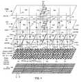
- FIG. 1is a schematic exploded perspective view of an integrated circuit structure with under-bump metallization and a distributed transistor fabricated in a checkerboard pattern.
- FIG. 2is a schematic cross-sectional view of the integrated circuit structure of FIG. 1 illustrating a single source-drain pair.
- FIG. 3is a schematic plan view of a portion of the substrate from FIG. 1 .
- FIG. 4is a schematic perspective view of a conductive area from the second conductive layer from the integrated circuit structure of FIG. 1 .
- FIG. 5is schematic plan view of the under-bump metallization layer with the solder bump shown in phantom.
- FIG. 6is a schematic cross-sectional view of the uppermost conductive layer and the under-bump metallization.
- FIG. 7is a schematic circuit diagram of the integrated circuit structure of FIG. 1 .
- FIG. 8is a schematic top view illustrating multiple adjacent under bump metallization areas arranged in a checkerboard pattern.
- FIG. 9is a schematic exploded perspective view of an integrated circuit structure with under-bump metallization and a distributed transistor fabricated in a pattern of parallel TOWS.
- FIG. 10is a schematic top view illustrating multiple adjacent under bump metallization areas arranged in parallel rows.
- FIG. 11is a block diagram of a switching regulator.
- FIG. 12is a circuit diagram illustrating electrical connections of an under-bump metallization layer.
- FIGS. 1 and 2illustrate one implementation of an integrated circuit structure 10 that can be used as a power switch.
- the structure 10includes a substrate 20 , a lowermost first conductive layer 30 , a middle second conductive layer 40 over the first conductive layer 20 , and a third conductive layer 50 over the second conductive layer 40 .
- an under-bump metallization (UBM) layer 60also termed a post-passivation metallization, is disposed over the third conductive layer 50 to provide electrical contact for a solder bump 80 .
- UBMunder-bump metallization
- the integrated circuit structurehas a first insulation layer 70 between the first conductive layer 30 and the second conductive layer 40 , a second insulation layer 72 between the second conductive layer 40 and the third conductive layer 50 , and a third insulation layer 74 , e.g., a passivation layer, between the third conductive layer 50 and the UBM layer 60 .
- the first conductive layer 30can be formed directly on the substrate 20 , although portions of the first conductive layer will be separated from conductive lines formed on the substrate 20 by another insulating layer.
- the conductive layerscan be formed of a metal, such as aluminum or copper, and the insulation layers can be formed of an oxide, such as silicon oxide, or a nitride.
- the substrate 20has a number of first doped regions 22 and a number of second doped regions 24 formed in, e.g., implanted into the surface layer of, a semiconductor substrate body 26 , e.g., a silicon body.
- the first doped regions 22 and second doped regions 24can be doped regions of a distributed transistor.
- the first doped regions 22serve as drain regions (“D”) and the second doped regions 24 serve as source regions (“S”).
- the drain regions 22 and the source regions 24can be arranged in an alternating checkerboard pattern in the substrate 20 as shown in FIG. 1 .
- the doped regions 22 and 24can be p-doped portions in an n-type substrate or well. If the switch is to be a NMOS transistor, then the doped regions 22 and 24 can be n-doped portions in a p-type substrate or well. If the switch is to be an LDMOS transistor, then the drain regions 22 can be n-doped portions in an n-type substrate or well, and the source region 24 can include both highly p-doped and highly n-doped portions in a lightly-p-doped p-body in the n-type substrate or well.
- a gate 200is also formed on the substrate 20 . Assuming that the doped regions 22 and 24 are arranged in a checkerboard pattern, the gate can include a first set of parallel gate lines 202 and a second set of parallel gate lines 204 . The two sets of gate lines 202 and 204 can intersect to form a rectangular array that surrounds each doped region 22 or 24 .
- the gate lines 202 and 204are formed of a conductive material 210 , such as polysilicon, that is separated from the semiconductor substrate body 26 by a gate insulator layer 212 , such as silicon dioxide.
- An additional insulator layer 214may be formed over the polysilicon to prevent a short circuit with the first conductive layer 30 .
- Apertures 216 in the additional insulator layer 214provide electrical contact between the first conductive layer 30 and the source and drain regions 22 and 24 in the substrate. Since the gate lines 202 and 204 extend off to the edges of the active area, the vias for electrical connections to the gate lines can be made near the edge of the switch, away from the interconnects for the source and drain.
- the first conductive layer 30includes a plurality of first regions 32 a and a plurality of second regions 32 b .
- the plurality of first regions 32 aare electrically isolated from the plurality of second regions 32 b .
- Each region 32 a and 32 boverlies multiple source and drain regions 22 and 24 .
- each region 32 a and 32 bis illustrated as overlying an identical sized array of doped regions, this is not required.
- Each first region 32 aincludes an interconnected conductive sheet 34 a with apertures 36 a .
- a conductive island 38 ais formed in each aperture 36 a .
- each second region 32 bincludes a conductive sheet 34 b with apertures 36 b and conductive islands 38 b formed in the aperture 36 b .
- the conductive islandsare electrically insulated from the conductive sheets.
- the sheets 34 a , 34 bcan be generally continuous, and the apertures 36 a , 36 b can be periodically spaced across the sheet.
- each first region 32 athe conductive islands 38 a overlie the source regions 24 , whereas the conductive sheet 34 a overlies and interconnects the drain regions 22 .
- the conductive islands 38 boverlie the drain regions 22 and the conductive sheet 34 b overlies and interconnects the source regions 24 .
- the combination of the conductive sheet 34 a and the conductive islands 38 bform a drain electrode
- the combination of the conductive sheet 34 b and the conductive islands 34 aform a source electrode.
- the doped regions and the first metal layer 30could be alternating stripes instead of a checkerboard pattern.
- the adjacent portions of the conductive sheets 34 a and 34 bcan form interleaved projections that overlie the drain and source regions 22 and 24 , respectively.
- conductive sheets 34 a and 34 bcan be implemented as alternating stripes, e.g., as shown in FIG. 9 .
- the second conductive layer 40includes a plurality of first conductive areas 42 a , a plurality of second conductive areas 42 b , a plurality of third conductive areas 44 c and a plurality of fourth conductive areas 42 d .
- Each plurality of conductive area 42 a , 42 b , 42 c and 42 dis electrically isolated from the other pluralities of conductive area within the second conductive layer 40 . Electrical isolation between adjacent conductive areas can be provided by portions of the insulation layer 72 .
- Each conductive area 42 a , 42 b , 42 c and 42 dcan be about the same size as an underlying conductive region 32 a or 32 b.
- each region 41 a or 41 bcan include an array of alternating conductive areas 42 a and 42 d or 42 b and 42 c , respectively.
- each region 41 a and 41 bis illustrated as including an identical sized array of conductive areas, this is not required.
- FIG. 1illustrates only a single first region 41 a and a single second region 41 b , there can be multiple regions 41 a and 41 b themselves arranged in an alternating pattern, e.g., a checkerboard pattern.
- the conductive areas 42 a , 42 b , 42 c and 42 d of the second conductive layer 40are connected by vias 220 - 226 (illustrated in phantom in FIG. 1 ) to the conductive islands 38 a and 38 b in the adjacent underlying regions 32 a and 32 b of the first conductive layer 30 .
- vias 220 - 226illustrated in phantom in FIG. 1
- the plurality of first areas 42 a of the second conductive layer 40are electrically coupled to the conductive islands 38 a in the underlying first regions 32 a of the first conductive layer 30 by vias 220 .
- the plurality of second areas 42 b of the second conductive layer 40are electrically coupled to the conductive islands 39 b in the underlying second regions 32 b of the first conductive layer 30 by vias 222 .
- the plurality of third areas 42 c of the second conductive layer 40are electrically coupled to the conductive islands 38 b in the underlying second regions 32 b of the second conductive layer 30 by vias 224 .
- the plurality of fourth areas 42 d of the second conductive layer 40are electrically coupled to the conductive islands 38 a in the underlying second regions 32 b of the first conductive layer 30 by vias 222 .
- Each conductive area 42 a , 42 b , 42 c and 42 dcan be a planar layer of a conductive material, such as a metal layer.
- each conductive area 42 a , 42 b , 42 c and 42 dcan be a substantially continuous plane.
- each conductive area 42 a , 42 b , 42 c and 42 dcan have one or more isolation structures 44 a , 44 b , 44 c and 44 d , respectively.
- each isolation structuree.g., isolation structure 44 a
- the first metal layer 30 and the second metal layer 40can be interconnected at their edges. If so, then adjacent portions of the conductive area 42 a , 42 b , 42 c and 42 d can form interleaved projections that overlie the projections from the conductive sheets 34 a and 34 b . In particular, projections from conductive areas 42 a and 42 d would overlie and be connected by vias to projections from conductive sheets 34 b , whereas projections from conductive areas 42 b and 42 c would overlie and be connected by vias to projections from conductive sheets 34 a .
- conductive sheets 34 a and conductive areas 42 b and 42 cwould form a laterally interconnected drain, whereas conductive sheets 34 b and conductive areas 42 a and 42 d would form a laterally interconnected source.
- projectionscan be formed in only one of the metal layers 30 , 40 .
- the third conductive layer 50includes at least one first region 52 a and at least one second region 52 b .
- the first region 52 ais electrically isolated from the second region 52 b .
- Each first region 52 a of the third conductive layer 50overlies a first region 41 a of the second conductive layer 40
- each second region 52 b of the third conductive layer 50overlies a second region 41 b of the second conductive layer 40 .
- the first region 52 awill overlie multiple conductive areas 42 a and 42 d
- the second region 52 bwill overlie multiple conductive areas 42 b and 42 c .
- each region 52 a or 52 bcan overlie an array of alternating conductive areas 42 a and 42 d or 42 b and 42 c , respectively.
- each region 52 a and 52 bis illustrated overlying an identical sized array of conductive areas, this is not required.
- FIG. 1illustrates the third conductive layer 50 as including only a single first region 52 a and a single second region 52 b , there can be multiple regions 52 a and 52 b arranged in an alternating pattern, e.g., a checkerboard pattern or a sequence of alternating rows.
- Each conductive region 52 a and 52 bcan a planar layer of a conductive material, such as a metal layer.
- each conductive region 52 a,d 52 bcan be a substantially continuous plane.
- each conductive region 52 a , 52 bcan have a number of isolation structures 54 a , 54 b , 54 c and 54 d .
- each isolation structure 54 a , 54 b , 54 c or 54 dincludes an aperture 56 in the conductive area within which is located a conductive island or via 58 that is electrically isolated from the surrounding conductive area.
- the conductive regions 52 a and 52 b of the third conductive layer 50are connected by vias 230 - 236 to the conductive sheets 34 a and 34 b in the underlying regions 32 a and 32 b of the first conductive layer 30 and to the conductive areas 42 a , 42 b , 42 c and 42 d of the second conductive layer (although FIG. 1 illustrates one via per connected area or region, there could be more than one).
- the first conductive region 52 ais electrically coupled to the underlying second conductive areas 42 b in the second conductive layer 40 by vias 230 .
- first conductive region 52 ais electrically coupled to the conductive sheets 34 a of the underlying first conductive regions 32 a of the first metal layer 30 by vias 232 that pass through the isolation structures 44 a in the first conductive areas 42 a of the second metal layer 40 .
- second conductive region 52 bis electrically coupled to the underlying fourth conductive areas 42 d in the second conductive layer 40 by vias 234 , and to the conductive sheets 34 b of the underlying second conductive regions 32 b of the first metal layer 30 by vias 236 that pass through the isolation structures 44 c in the third conductive areas 42 c of the second metal layer 40 .
- the first conductive region(s) 52 ais part of the drain electrode
- the second conductive region(s) 52 bis part of the source electrode.
- lateral protrusions 240At the edge of the first conductive region 52 a that is adjacent the second conductive region 52 b are one or more lateral protrusions 240 , such as a plurality of rectangular protrusions.
- second conductive region 52 b that is adjacent the first conductive region 52 aare one or more lateral protrusions 242 , such as a plurality of rectangular protrusions.
- the rectangular protrusions 240 , 242 of the two conductive regions 52 a , 52 b areascan interlace in an alternating pattern to form a region of interdigitated protrusions at the common edge of the conductive regions 52 a and 52 b.
- the lateral protrusions 240 of the first conductive region 52 a of the third metal layercan vertically underlie protrusions 252 from a second conductive area 62 b of the UBM layer 60 .
- Electrical coupling between the lateral protrusions 240 of the first conductive region 52 a of the third metal layer 50 and the protrusions 252 from the second conductive area 62 b of the UBM layer 60can be provided by vias 260 .
- the lateral protrusions 242 of the second conductive region 52 b of the third metal layercan vertically underlie protrusions 250 from a first conductive area 62 a of the UBM layer 60 .
- Electrical coupling between the lateral protrusions 242 of the second conductive region 52 b of the third metal layer 50 and the protrusions 250 from the first conductive area 62 a of the UBM layer 60can be provided by vias 262 .
- the UBM layer 60is similar to the third conductive layer 50 , and includes one or more first conductive areas 62 a and one or more second conductive areas 62 b , with the first areas 62 a electrically isolated from the second areas 62 b .
- the first conductive area 62 a and the second conductive area 62 bcan simply be physically separated structures on the top surface of the integrated circuit chip (e.g., separated by an air gap), or an insulation layer can be provided in the lateral space between the two areas 62 a and 62 b.
- the UBM layer 60can include a conductive pad layer 280 , such as a metal layer, e.g., aluminum, on which is formed a conductive intermediate layer 282 , such as nickel-vanadium alloy.
- a conductive pad layer 280such as a metal layer, e.g., aluminum
- a conductive intermediate layer 282such as nickel-vanadium alloy.
- the aluminum layercan be 1 micron thick, and the copper layer can be 0.8 micron or more, e.g., up to 14 microns thick.
- the intermediate layer 282provides a diffusion barrier.
- the UBMincludes a conductive pad layer, such as a metal layer, e.g., titanium.
- a conductive pad layersuch as a metal layer, e.g., titanium.
- a thin conductive seed layere.g., of copper
- a thick conductive outer layere.g., of copper
- the thick conductive outer layercan be more than 6 microns thick, e.g., more than 9 microns thick, e.g., about 12 to 14 microns thick.
- the thick copper layerprevents electrical discontinuity from developing due to consumption of the copper layer during formation of the bump.
- a metal solder bump 290is formed on the thick conductive outer layer 286 .
- One metal solder bump 290can be provided per conductive area 62 a or 62 b , e.g., particularly if the conductive areas 62 a and 62 b are arranged in a checkerboard pattern.
- more than one metal solder bump 290e.g., a row of bumps, can be provided per conductive area 62 a or 62 b , e.g., particularly if the conductive areas 62 a and 62 b are arranged in alternating TOWS.
- an edge of the first conductive area 62 a adjacent the second conductive area 62 bhas one or more lateral protrusions 250 , e.g., as a plurality of rectangular protrusions that extended toward the second conductive area 62 b .
- an edge of the second conductive area 62 b adjacent the first conductive area 62 ahas one or more lateral protrusions 252 , e.g., a plurality of rectangular protrusions that extended toward the first conductive area 62 a .
- the rectangular protrusions of the two conductive areascan interlace in an alternating pattern to form a region of inter-digited protrusions at the common edge of the conductive areas 62 a and 62 b.
- the first conductive area 62 a of the UBM layer 60may substantially overlap the first conductive region 52 a of the third metal layer 50 except for the extended regions.
- the second conductive region 64 b of the UBM layer 60may substantially overlap the second conductive area 52 b of the third metal layer 50 except for the extended regions.
- the lateral protrusions 250 of the first conductive area 62 a of the UBM layer 60overlap the lateral protrusions 242 of the second conductive region 52 a of the third metal layer 50 , and vias 262 provide electrical couplings between the overlapped areas.
- the lateral protrusions 252 of the second conductive area 62 b of the UBM layer 60overlap the lateral protrusions 240 of the first conductive region 52 a
- vias 260provide electrical couplings between the overlapped areas.
- the overlapping protrusions and viasform an “interstitching” structure that electrically couples the first conductive region 52 a of the third metal layer 50 with the second conductive area 62 b of the UBM layer 60 , and electrically couples the second conductive region 52 b of the third metal layer 50 with the first conductive region 62 a of the UBM layer 60 .
- the conductive areas 62 a and 62 b of the UBM 60are connected by vias 270 - 276 to the conductive sheets 34 a and 34 b in the regions 32 a and 32 b of the first conductive layer 30 and to the conductive areas 42 a , 42 b , 42 c and 42 d of the second conductive layer that underlie the particular conductive area (although FIG. 1 illustrates one via per connected area or region, there could be more than one).
- the first conductive area 62 a of the UBM layer 60is electrically coupled to the underlying first conductive areas 42 a in the second conductive layer 40 by vias 270 that pass through the isolation structures 54 a in the first conductive region 52 a of the third metal layer 50 .
- first conductive area 62 a of the UBM layer 60is electrically coupled to the conductive sheets 34 b of the underlying second conductive regions 32 b of the first metal layer 30 by vias 272 that pass through the isolation structures 54 b in the first conductive region 52 a of the third metal layer 50 and through the isolation structures 44 b in the second conductive areas 42 b of the second metal layer 40 .
- the second conductive area 62 b of the UBM layer 60is electrically coupled to the underlying third conductive areas 42 c in the second conductive layer 40 by vias 274 that pass through the isolation structures 54 c in the second conductive region 52 b of the third metal layer 50
- the second conductive area 62 b of the UBM layer 60is electrically coupled to the conductive sheets 34 a of the underlying first conductive regions 32 a of the first metal layer 30 by vias 276 that pass through the isolation structures 54 d in the second conductive region 52 b of the third metal layer 50 and through the isolation structures 44 d in the fourth conductive areas 42 d of the second metal layer 40 .
- the first conductive area 62 a of the UBM layer 60becomes the source electrode
- the second conductive area 62 b of the UBM layer 60becomes the drain electrode.
- FIG. 1illustrates an implementation in which the drain regions 22 are electrically coupled to the first conductive region 52 a of the third metal layer 50 and the second conductive area 62 b of the UBM layer 60 , the source regions 24 are electrically coupled to the second conductive region 52 b of the third metal layer 50 and the first conductive area 62 a of the UBM layer 60 , and third metal layer 50 and the UBM layer 62 are connected by an interstitching that keeps the drain and source electrodes electrically isolated.
- FIG. 7A schematic circuit diagram of this configuration is illustrated in FIG. 7 .
- FIG. 1illustrates the UBM layer 60 with just two adjacent conductive areas 62 a and 62 b
- the integrated circuit structurecan be fabricated with multiple interconnected areas.
- the conductive areas 62 a and 62 bcan be formed in a checkerboard pattern, with interstitching connecting the second and third conductive layers at the adjacent boarder of each pair of conductive areas.
- the conductive areas 62 a and 62 bcan be arranged in alternating rows, columns, or in some other pattern. This permits the source and drain pads on the top surface of a chip to be arranged in rows, columns, in a checkerboard, or in some other pattern.
- the integrated circuit structure of the present inventioncouples the source and drain regions of the distributed transistor to the conductive planes of the UBM layer 60 with short lateral interconnects in the first and second conductive layers.
- the third conductive layer 50 and the UBM layer 60can be relatively thick, they can carry large amounts of current (in comparison to the buried first and second conductive layers 30 and 40 , which should be thinner).
- the UBM layer 60can carry current laterally to vias (e.g., vias that are not directly under the solder bump) with lower resistance than the first and second conductive layers.
- the planar current flow in the third conductive layer 50 and UBM layer 60 and the short path of direct vertical interconnectsreduce the current flow density and resistance of interconnects.
- the inventiontherefore reduces power loss of circuits and improves the reliability of circuits and devices. If conducting pads can be placed above the functional area, the invention reduces area needed for providing conducting pads on an IC chip and produces cheaper dies in a smaller package than a traditional IC structure.
- FIGS. 9 and 10illustrate another implementation of an integrated circuit structure 310 that can be used as a power switch. Except as set forth below, the integrated circuit structure of FIGS. 9 and 10 can be constructed similarly to the structure of FIGS. 1-8 .
- the structure 310includes a substrate 320 , a lowermost first conductive layer 310 , a middle second conductive layer 340 over the first conductive layer 320 , and a third conductive layer 350 over the second conductive layer 340 .
- an under-bump metallization (UBM) layer 360is disposed over the third conductive layer 350 to provide electrical contact for a solder bump 380 .
- the substrate 320has a number of first doped regions 322 and a number of second doped regions 324 formed in, e.g., implanted into the surface layer of, a semiconductor substrate body, e.g., a silicon body.
- the first doped regions 322 and second doped regions 324can be doped regions of a distributed transistor.
- the first doped regions 322serve as drain regions (“D”) and the second doped regions 324 serve as source regions (“S”).
- the drain regions 322 and the source regions 324can be arranged in alternating rows as shown in FIG. 9 .
- the gatecan include parallel gate lines 328 that run between each pair of adjacent doped region 322 and 324 . Since the gate lines 328 extend off to the opposing edges of the active area, the vias for electrical connections to the gate lines can be made near the edge of the switch, away from the interconnects for the source and drain.
- the first conductive layer 330includes a plurality of first regions 332 a and a plurality of second regions 332 b .
- conductive strips 334 aoverlie the source regions 324 and conductive strips 336 a overlie the drain regions 322 .
- conductive strips 334 boverlie the drain regions 322 and conductive strips 336 b overlie the source regions 324 .
- the combination of the conductive strips 334 a and the conductive strips 336 bform a source electrode
- the combination of the conductive strips 334 b and the conductive strips 336 aform a drain electrode.
- Each region 332 a and 332 boverlies multiple source and drain regions 322 and 324 , e.g., multiple rows of alternating regions. Adjacent conductive strips are electrically insulated from each other. Although each region 332 a and 332 b is illustrated as overlying an identical sized group of doped regions, this is not required. Optionally, one or both sets of conductive strips within a region can be electrically connected within the first conductive layer. For example, the strips 334 a could extend past the ends of strips 336 a and be connected to a conductive bar extending along one edge of the region 332 a perpendicular to the strips.
- the second conductive layer 340includes a plurality of first conductive areas 342 a and a plurality of second conductive areas 342 b (only one of each conductive area is illustrated). Each plurality of conductive area 342 a , 342 b is electrically isolated from the other plurality of conductive areas within the second conductive layer 340 . Each conductive area 342 a , 342 b can be about the same size as an underlying conductive region 332 a or 332 b , and the conductive areas 342 a , 342 b can be arranged in alternating rows.
- the conductive areas 342 a of the second conductive layer 40are connected by vias 338 a to the conductive strips 334 a in the adjacent underlying regions 332 a of the first conductive layer 330 .
- the conductive areas 342 b of the second conductive layer 40are connected by vias 338 b to the conductive strips 334 b in the adjacent underlying regions 332 b of the first conductive layer 330 .
- not every viais illustrated.
- the combination of the first conductive areas 342 aforms the source electrode
- the combination of the second conductive areas 342 bforms the drain electrode
- Each conductive area 342 a and 342 bcan be a planar layer of a conductive material, such as a metal layer.
- each conductive area 342 a , 342 bcan be a substantially continuous plane.
- each conductive area 342 a and 342 bcan have one or more isolation structures 344 a and 344 b , respectively.
- Each isolation structureincludes an aperture in the conductive area and a conductive island or via in the aperture that is electrically isolated from the surrounding conductive area.
- the third conductive layer 350includes at least one first region 352 a and at least one second region 352 b .
- the first region 352 ais electrically isolated from the second region 352 b .
- Each first region 352 a of the third conductive layer 350overlies a first conductive area 342 a of the second conductive layer 340
- each second region 352 b of the third conductive layer 350overlies a second conductive area 342 b of the second conductive layer 340 .
- Each conductive region 352 a and 352 bcan a planar layer of a conductive material, such as a metal layer.
- each conductive region 352 a , 352 bcan be a substantially continuous plane.
- each conductive region 352 a , 352 bcan have a number of isolation structures 354 a , 354 b , respectively.
- each isolation structure 354 a , 354 bincludes an aperture 356 in the conductive area within which is located a conductive island or via 358 that is electrically isolated from the surrounding conductive area.
- the isolation structures 354 a , 354 bcan be significantly larger than the isolation structures 344 a , 344 b so as to accommodate larger current flow per structure.
- the conductive regions 352 a and 352 b of the third conductive layer 50are connected by vias 382 , 384 to the conductive strips 336 a and 336 b in the underlying regions 332 a and 332 b of the first conductive layer 330 .
- the first conductive region 352 ais electrically coupled to the conductive strips 336 a of the underlying first conductive regions 332 a of the first metal layer 30 by vias 382 that pass through the isolation structures 344 a in the first conductive areas 342 a of the second metal layer 40 .
- the second conductive region 352 bis electrically coupled to the conductive strips 336 b of the underlying first conductive regions 332 b of the first metal layer 30 by vias 384 that pass through the isolation structures 344 b in the second conductive areas 342 b of the second metal layer 340 .
- the first conductive region(s) 352 ais part of the drain electrode, whereas the second conductive region(s) 352 b is part of the source electrode.
- the density of vias 338 a , 338 b per unit length of the conductive strips 334 a , 334 bcan be greater than the density of vias 382 , 384 per unit length of the conductive strips 336 a , 336 b.
- lateral protrusions 240At the edge of the first conductive region 352 a that is adjacent the second conductive region 352 b are one or more lateral protrusions 240 , such as a plurality of rectangular protrusions.
- second conductive area 342 a that is adjacent the first conductive region 352 aare one or more lateral protrusions 242 , such as a plurality of rectangular protrusions.
- the rectangular protrusions 240 , 242 of the two conductive regions 352 a , 352 b areascan interlace in an alternating pattern to form a region of interdigitated protrusions at the common edge of the conductive regions 352 a and 352 b.
- the UBM layer 360includes one or more first conductive areas 362 a and one or more second conductive areas 362 b , with the first areas 362 a electrically isolated from the second areas 362 b .
- An edge of the first conductive area 362 a adjacent the second conductive area 362 bhas one or more lateral protrusions 250 , e.g., as a plurality of rectangular protrusions that extended toward the second conductive area 362 b .
- an edge of the second conductive area 362 b adjacent the first conductive area 362 ahas one or more lateral protrusions 252 , e.g., a plurality of rectangular protrusions that extended toward the first conductive area 362 a .
- the rectangular protrusions of the two conductive areascan interlace in an alternating pattern to form a region of interdigitated protrusions at the common edge of the conductive areas 362 a and 362 b.
- the first conductive area 362 a of the UBM layer 360can substantially overlap the first conductive region 352 a of the third metal layer 350 except for the extended regions.
- the second conductive region 362 b of the UBM layer 360can substantially overlap the second conductive area 352 b of the third metal layer 350 except for the extended regions.
- the lateral protrusions 250 of the first conductive area 362 a of the UBM layer 360overlap the lateral protrusions 242 of the second conductive region 352 a of the third metal layer 350 , and vias 262 provide electrical couplings between the overlapped areas.
- the lateral protrusions 252 of the second conductive area 362 b of the UBM layer 360overlap the lateral protrusions 240 of the first conductive region 352 a , and vias 260 provide electrical couplings between the overlapped areas.
- the overlapping protrusions and viasform an “interstitching” structure that electrically couples the first conductive region 352 a of the third metal layer 350 with the second conductive area 362 b of the UBM layer 360 , and electrically couples the second conductive region 352 b of the third metal layer 350 with the first conductive region 362 a of the UBM layer 360 .
- the conductive areas 362 a and 362 b of the UBM 360are connected by vias 386 , 388 to the conductive areas 342 a and 342 b of the second conductive layer 340 that underlie the particular conductive area (although FIG. 1 illustrates two vias per connected area or region, there could be just one or more than two).
- the first conductive area 362 a of the UBM layer 360is electrically coupled to the underlying first conductive areas 342 a in the second conductive layer 340 by vias 386 that pass through the isolation structures 354 a in the first conductive region 352 a of the third metal layer 350 .
- the second conductive area 362 b of the UBM layer 360is electrically coupled to the underlying second conductive areas 342 b in the second conductive layer 340 by vias 388 that pass through the isolation structures 354 b in the second conductive region 352 b of the third metal layer 350 .
- the first conductive area 362 a of the UBM layer 360becomes the source electrode
- the second conductive area 362 b of the UBM layer 360becomes the drain electrode.
- the density of vias 382 , 384can be greater than the density of vias 386 , 388 .
- the vias 344 a , 344 b from the third metal layer 350 to the first metal layer 330can be omitted in regions where the large vias 348 connects the UBM layer 360 and the second metal layer 340 .
- the edges of the second metal layer 340can be interstitched with the edges of the third metal layer 350 .
- portions of the projections 240 of the first conductive region 352 a in the third metal layer 350can extend over and be connected by vias to the second conductive area 342 b in the second metal layer 340
- portions of the projections 242 of the second conductive region 352 b in the third metal layer 350can extend over and be connected by vias to the first conductive area 342 a in the second metal layer 340 .
- the projectionsare formed in only one of the metal layers 340 , 350 .
- the present inventionmay be implemented to various kinds of IC chips for providing external couplings to the IC chips. Without limiting the scope of the present invention, the implementation of the invention to an IC chip for voltage regulators is illustrated in detail below as an example.
- Voltage regulatorssuch as DC-to-DC converters, are used to provide stable voltage sources for electronic systems.
- Switching voltage regulators(or simply “switching regulators”) are known to be an efficient type of DC-to-DC converter.
- a switching regulatorgenerates an output voltage by converting an input DC voltage into a high frequency voltage waveform, and filtering the high frequency voltage waveform to generate the output DC voltage.
- the switching regulatorincludes a switch for alternately coupling and decoupling an input DC voltage source, such as a battery, to a load, such as an IC chip.
- An output filtertypically including an inductor and a capacitor that are provided between the input voltage source and the load, filters the output of the switch and thus provides the output DC voltage.
- a pulse modulatorsuch as a pulse width modulator or a pulse frequency modulator, typically controls the switch.
- an implementation of a switching regulator 110is coupled to a DC input voltage source 112 , such as a battery, by an input terminal 120 .
- the switching regulator 110is also coupled to a load 114 , such as an IC chip, by an output terminal 124 .
- the switching regulator 110serves as a DC-to-DC converter between the input terminal 120 and the output terminal 124 .
- the switching regulator 110includes a switching circuit 116 that serves as a power switch for alternately coupling and decoupling the input terminal 120 to an intermediate terminal 122 .
- the switching circuit 116includes a rectifier, such as a switch or diode, coupling the intermediate terminal 122 to ground.
- the switching circuit 116 and the output filter 126may be configured in a buck converter topology with a first transistor 130 connected between the input terminal 120 and the intermediate terminal 122 and a second transistor 132 connected between ground and the intermediate terminal 122 .
- the first transistor 130may be a P-type MOS (PMOS) device or N-type LDMOS device
- the second transistor 132may be an N-type MOS (NMOS) device or N-type LDMOS device, and other permutations of PMOS, NMOS, P-type LDMOS and N-type LDMOS devices are possible.
- the switching regulator 110may also include an input capacitor 138 connecting the input terminal 122 to ground.
- the switching regulatoralso includes a controller assembly with a pulse modulator 118 for controlling the operation of the switching circuit 116 .
- the pulse modulator 118causes the switching circuit 116 to generate an intermediate voltage having a rectangular waveform at the intermediate terminal 122 .
- the pulse modulator 118 and the switching circuit 116are illustrated and described below as a pulse width modulator, the invention is also applicable to various pulse frequency modulation schemes.
- the intermediate terminal 122is coupled to the output terminal 124 by an output filter 126 .
- the output filter 126filters the rectangular waveform of the intermediate voltage at the intermediate terminal 122 into a substantially DC output voltage at the output terminal 124 .
- the output filter 126includes an inductor 134 connected between the intermediate terminal 122 and the output terminal 124 and a capacitor 136 connected in parallel with the load 114 .
- the voltage source 112supplies energy to the load 114 and the inductor 134 via the first transistor 130 .
- transistor 132is closed and the inductor 134 supplies the energy.
- the resulting output voltage V outis a substantially DC voltage.
- switching circuit 116 and the output filter 126are illustrated in a buck converter topology, the invention is also applicable to other switching voltage regulator topologies, such as a boost converter topology, a buck-boost converter topology, or a variety of transformer coupled topologies.
- the output voltageis regulated, or maintained at a substantially constant level, by a feedback loop in the controller assembly that includes a feedback circuit 128 .
- the feedback circuit 128includes circuitry that measures the output voltage and/or the current passing through the intermediate terminal. The measured voltage and current are used to control the pulse modulator 118 so that the output voltage at the output terminal 124 remains substantially constant.
- the conductive routings of the present inventioncan be used in the switching circuit 116 to provide a flip-chip package that includes the switching circuit and provides external couplings.
- each switch in the switching circuit 116is fabricated as a distributed array of parallel transistors, and the conductive routing structures discussed above can carry current from the doped regions to the conducting pads on the surface of the chip.
- the second transistor 132can include rectangular n-doped source regions 24 and drain regions 22 laid out in a checkerboard pattern in a p-type well or substrate.
- the first transistor 130is implemented as a p-channel device, is can include alternating rectangular p-doped source regions and drain regions in an n-type well or substrate.
- the first transistor 130is implemented as an re-channel device, it can include alternating rectangular n-doped source regions and drain regions in a p-type well or substrate.
- a grid-like gatemay be implemented to separate each pair of source and drain regions. Electrical connection to the gate can be provided at the peripheral edge of the chip.
- the routing structureis generally applicable to supply power to any integrated device, particular integrated devices with regular arrays of circuitry needing connection to an input voltage and ground.
- one region of the UBMcan be electrically connected to an input voltage line of a circuit block and the other region of the UBM can be electrically connected to the ground line of the circuit block.
- the first region of the UBMis connected as V in to a source of a high-side transistor 142 and another region of the UBM is connected as ground to a source of a low-side transistor 144 .
- isolation structuresare discussed and illustrated as including one conductive island or via, the isolation structures can include multiple vias in parallel.
- drawingsillustrate hemispherical solder bumps 80 , 390 , other flip-chip interconnects can be used, such as stud bumps or copper pillars, and the solder bumps can solder balls or be formed in other shapes such as, for example, studs or columnar members.
Landscapes
- Physics & Mathematics (AREA)
- Condensed Matter Physics & Semiconductors (AREA)
- General Physics & Mathematics (AREA)
- Engineering & Computer Science (AREA)
- Computer Hardware Design (AREA)
- Microelectronics & Electronic Packaging (AREA)
- Power Engineering (AREA)
- Internal Circuitry In Semiconductor Integrated Circuit Devices (AREA)
Abstract
Description
This application is a continuation of U.S. patent application Ser. No. 13/454,968, filed Apr. 24, 2012, which claims priority to and is a continuation of U.S. patent application Ser. No. 12/343,261, filed Dec. 23, 2008, which claims priority to U.S. Provisional Application Ser. No. 61/017,139, filed on Dec. 27, 2007, the entire disclosures of which are incorporated by reference.
The present invention relates generally to conductive routings in integrated circuits, and in one aspect, to conductive routings in integrated circuits used as power switches.
Integrated circuits (“IC”), which generally refer to electronic circuits formed on a silicon or other semiconductor substrate, have widespread application in modern electronic systems. An IC chip may contain circuit devices, such as transistors, and electrical interconnects to electrically couple the circuit devices. An outer surface of the IC chip may also contain conductive pads for providing electrical coupling of the chip to external devices, such as voltage sources and control circuits. Traditionally, electrical connection between the transistors in the semiconductive substrate and the conductive pads is accomplished through the use of multiple conductive layers that are formed over the semiconducting substrate of the integrated circuit chip but below an insulative layer that supports the conductive pads (an aperture in the insulative layer can provide electrical coupling of the contact pad to the uppermost conductive layer). For example, an integrated circuit chip may have metal lines and vias that electrically couple the source and drain regions of the transistors to the conducting pads of the integrated circuit chip.
Voltage regulators, such as DC to DC converters, are used to provide stable voltage sources for electronic systems. Switching voltage regulators are known to be an efficient type of DC to DC converter. Such voltage regulators typically include a power switch to generate a rectangular-wave voltage that is filtered to provide the output DC voltage.
Conventionally, the power switch was fabricated as an integrated circuit chip with wire bond packaging. More recently, the power switch has been fabricated as an integrated circuit chip with flip-chip packaging (in which solder bumps are placed on the top surface of the chip, and the chip is mounted upside down with the solder bumps connected directly to a printed circuit board, interposer, or to a package).
In one aspect, an integrated circuit structure includes a first conductive layer and an under bump metallization layer over the first conductive layer. The first conductive layer has a first conductive region and a second conductive region electrically isolated from the first conductive region. The under bump metallization layer has a first conductive area and a second conductive area electrically isolated from the first conductive area, the first conductive area substantially located over the first conductive region and the second conductive area substantially located over the second conductive region. At least one of the first conductive area or the first conductive region includes a first protrusion extending toward the second conductive area or second conductive region, respectively. Conductive vias connect the first conductive region to the second conductive area and connect the second conductive region to the first conductive area, and the conductive vias include at least one via connected to the first protrusion.
Implementations can include one or more of the following features. The first conductive area may include the first protrusion extending toward the second conductive area. The first conductive region may include a second protrusion extending toward the second conductive region, and the conductive vias may include at least one via connected to the second protrusion. The first conductive region may include the first protrusion extending toward the second conductive region. A first flip-chip interconnect may be on the first conductive area of the under bump metallization layer, and a second flip-chip interconnect may be on the second conductive area of the under bump metallization layer. The first flip-chip interconnect and second flip-chip interconnect may be solder bumps, solder balls, copper pillars or stud bumps. The first conductive region may have a plurality of first protrusions extending toward the second conductive region, and the second conductive region may have a plurality of second protrusions extending toward the first conductive region. The first conductive area may have a plurality of third protrusions extending toward the second conductive area, and the second conductive area may have a plurality of fourth protrusions extending toward the first conductive area. A plurality of first conductive vias may connect the plurality of first protrusions to the plurality of fourth protrusions, and a plurality of second conductive vias may connect the plurality of second protrusions to the plurality of third protrusions. The first conductive area may have a plurality of first protrusions extending toward the second conductive area, and the second conductive area may have a plurality of second protrusions extending toward the first conductive area.
The under bump metallization may include a contact layer to contact a portion of the first conductive layer and an outer layer. An intermediate layer may be between the contact layer and the outer layer. The intermediate layer may include a diffusion-blocking material. The contact layer may include aluminum, the intermediate layer may include a nickel vanadium alloy, and the outer layer may include copper. The contact layer may be titanium and the outer layer may be copper. The outer layer may be a metal layer, e.g., copper, having a thickness greater than 6 microns.
The integrated circuit structure may further comprise a substrate under the first conductive layer. The substrate may have a first distributed transistor with a first plurality of doped source regions and a first plurality of doped drain regions, and the first conductive region and the second conductive area may be electrically coupled to the first plurality of doped source regions and the second conductive region and the first conductive area may be electrically coupled to the first plurality of doped drain regions. The first plurality of doped source regions and the first plurality of doped drain regions may be are arranged in an alternating pattern in the substrate. The substrate may have a second distributed transistor with a second plurality of doped source regions and a second plurality of doped drain regions arranged in an alternating pattern in the substrate. The first conductive layer may have a third conductive region and a fourth conductive region electrically isolated from the third conductive region. The under bump metallization layer may have a third conductive area and a fourth conductive area electrically isolated from the third conductive area, the third conductive area substantially located over the third conductive region and the second conductive area substantially located over the fourth conductive region. At least one of the third conductive area or the third conductive region may include a second protrusion extending toward the fourth conductive area or fourth conductive region, respectively. The conductive vias may connect the third conductive region to the fourth conductive area and connect the fourth conductive region to the third conductive area. The conductive vias may include at least one via connected to the second protrusion. The third conductive region and the fourth conductive may be electrically coupled to the second plurality of doped source regions and the fourth conductive region and the third conductive area electrically coupled to the second plurality of doped drain regions. The first conductive area may be electrically coupled to the third conductive area. The first conductive area may be electrically coupled to the fourth conductive area. Thee second conductive area may be electrically coupled to the fourth conductive area.
A second conductive layer may be between the first conductive layer and the substrate. The second conductive layer may include a plurality of first conductive portions and a plurality of second conductive portions disposed below the first conductive region, and may include plurality of third conductive portions and a plurality of fourth conductive portions disposed below the first conductive region. A third plurality of vias may connect the first conductive region to the plurality of first conductive portions, and a fourth plurality of vias may connect the second conductive region to the plurality of third conductive portions. A fifth plurality of vias may connect the first conductive area to the plurality of second conductive portions, and a sixth plurality of vias may connect the second conductive area to the plurality of fourth conductive portions. A first flip-chip interconnect may be on the first conductive area of the under bump metallization layer, a second flip-chip interconnect may be on the second conductive area of the under bump metallization layer, a third flip-chip interconnect may be on the third conductive area of the under bump metallization layer, and a fourth flip-chip interconnect may be on the fourth conductive area of the under bump metallization layer.
In another aspect, an integrated circuit structure includes a first conductive layer and a second conductive layer over the first conductive layer. The first conductive layer has a first conductive region and a second conductive region electrically isolated from the first conductive region. The second conductive layer has a first conductive area and a second conductive area electrically isolated from the first conductive area, the first conductive area substantially located over the first conductive region and the second conductive area substantially located over the second conductive region. Only one of the first conductive area or the first conductive region includes a first protrusion extending toward the second conductive area or second conductive region, respectively. Conductive vias connect the first conductive region to the second conductive area and connect the second conductive region to the first conductive area. The conductive vias include at least one via connected to the first protrusion.
Implementations can include one or more of the following features. The first conductive area may include the first protrusion extending toward the second conductive area. The first conductive region may include the first protrusion extending toward the second conductive region. The first conductive region may have a plurality of first protrusions extending toward the second conductive region, and the second conductive region may have a plurality of second protrusions extending toward the first conductive region. The first conductive area may have a plurality of third protrusions extending toward the second conductive area, and the second conductive area may have a plurality of fourth protrusions extending toward the first conductive area. A plurality of first conductive vias may connect the plurality of first protrusions to the plurality of fourth protrusions, and a plurality of second conductive vias may connect the plurality of second protrusions to the plurality of third protrusions. The first conductive area may have a plurality of first protrusions extending toward the second conductive area, and the second conductive area may have a plurality of second protrusions extending toward the first conductive area. The integrated circuit structure may include a substrate under the first conductive layer. The substrate may have a first plurality of doped source regions and a second plurality of doped drain regions, and the first conductive region and the second conductive area may be electrically coupled to the first plurality of doped source regions and the second conductive region and the first conductive area may be electrically coupled to the first plurality of doped drain regions.
In another aspect, an integrated circuit structure includes a first conductive layer, a second conductive layer under the first conductive layer, and an under bump metallization layer over the first conductive layer. The first conductive layer has a first conductive region and a second conductive region electrically isolated from the first conductive region. The second conductive layer includes a first conductive portion and a second conductive portion electrically isolated from the first conductive portion, the first conductive portion disposed below the first conductive region, the second conductive portion disposed below the second conductive region. The under bump metallization layer has a first conductive area and a second conductive area electrically isolated from the first conductive area, the first conductive area substantially located over the first conductive region and the second conductive area substantially located over the second conductive region. A first conductive via connects the first conductive area to the first conductive portion. The first conductive via passes through an aperture in and is electrically isolated from the first conductive region. Conductive vias connect the first conductive region to the second conductive area, connect the second conductive region to the first conductive area, connect the first conductive portion to the second conductive region, and connect the second conductive portion to the first conductive region.
Implementations can include one or more of the following features. A second conductive via may connect the second conductive area to the second conductive portion. The second conductive via may pass through an aperture in and be electrically isolated from the second conductive region.
In another aspect, an integrated circuit structure includes a first conductive layer, a second conductive layer under the first conductive layer, and an under bump metallization layer over the first conductive layer. The first conductive layer has a first conductive region and a second conductive region electrically isolated from the first conductive region. The second conductive layer has a first conductive portion and a second conductive portion electrically isolated from the first conductive portion, the first conductive portion disposed below and substantially overlapping the first conductive region, the second conductive portion disposed below and substantially overlapping the second conductive region. The under bump metallization layer has a first conductive area and a second conductive area electrically isolated from the first conductive area, the first conductive area disposed over and substantially overlapping the first conductive region and the second conductive area disposed over the second conductive region. At least one of the first conductive area, first conductive region or first conductive portion includes a protrusion extending toward the second conductive region, second conductive area or second conductive portion, respectively. Conductive vias connect the first conductive region to the second conductive area, connect the second conductive region to the first conductive area, connect the first conductive portion to the second conductive region, and connect the second conductive portion to the first conductive region. The conductive vias including at least one via connected to the protrusion.
In another aspect, an integrated circuit structure includes a first conducive layer and an under bump metallization layer over the first conductive layer. The first conductive layer has a first conductive region and a second conductive region electrically isolated from the first conductive region, the first conductive region having a first protrusion extending toward the second conductive region. The under bump metallization layer has a first conductive area and a second conductive area electrically isolated from the first conductive area. The first conductive area is substantially located over the first conductive region and the second conductive area is substantially located over the second conductive region. The first conductive area has a second protrusion extending toward the second conductive area. A first conductive via connects the first protrusion to the second conductive area, and a second conductive via connects the second protrusion to the second conductive region.
Advantages may include the following. The lengths of conductive routings from doped regions in a substrate to conducting pads can be shortened. Interconnection resistance and power loss can be reduced. In addition, the conductive routing structure of the present invention can permit planar current flow so as to reduce resistance and current flow density, thereby increasing the reliability of circuits and devices. The area needed for providing conducting pads on an IC chip can be reduced. As a result, a chip implemented with the present invention can have cheaper dies in a smaller package, lower power loss, and shorter conductive path lengths than a traditional IC structure. The area available for functional devices in a chip, therefore, can be increased. At the same time, the performance of devices and circuits on a chip can be increased as a result of reduced resistance and power loss.
The details of one or more embodiments are set forth in the accompanying drawings and the description below. Other features, objects, and advantages of the invention will be apparent from the description and drawings, and from the claims.
Referring toFIGS. 1-3 , thesubstrate 20 has a number of firstdoped regions 22 and a number of seconddoped regions 24 formed in, e.g., implanted into the surface layer of, asemiconductor substrate body 26, e.g., a silicon body. The firstdoped regions 22 and seconddoped regions 24 can be doped regions of a distributed transistor. In the illustrated implementation, the firstdoped regions 22 serve as drain regions (“D”) and the seconddoped regions 24 serve as source regions (“S”). Thedrain regions 22 and thesource regions 24 can be arranged in an alternating checkerboard pattern in thesubstrate 20 as shown inFIG. 1 .
If the switch is to be a PMOS transistor, then thedoped regions doped regions drain regions 22 can be n-doped portions in an n-type substrate or well, and thesource region 24 can include both highly p-doped and highly n-doped portions in a lightly-p-doped p-body in the n-type substrate or well.
Agate 200 is also formed on thesubstrate 20. Assuming that the dopedregions parallel gate lines 202 and a second set of parallel gate lines204. The two sets ofgate lines region conductive material 210, such as polysilicon, that is separated from thesemiconductor substrate body 26 by agate insulator layer 212, such as silicon dioxide. Anadditional insulator layer 214 may be formed over the polysilicon to prevent a short circuit with the firstconductive layer 30.Apertures 216 in theadditional insulator layer 214 provide electrical contact between the firstconductive layer 30 and the source and drainregions gate lines
Returning toFIG. 1 , the firstconductive layer 30 includes a plurality offirst regions 32aand a plurality ofsecond regions 32b. The plurality offirst regions 32aare electrically isolated from the plurality ofsecond regions 32b. Eachregion regions region
Eachfirst region 32aincludes an interconnectedconductive sheet 34awith apertures36a. Aconductive island 38ais formed in each aperture36a. Similarly, eachsecond region 32bincludes aconductive sheet 34bwithapertures 36bandconductive islands 38bformed in theaperture 36b. Thus, the conductive islands are electrically insulated from the conductive sheets. Thesheets apertures 36a,36bcan be periodically spaced across the sheet.
In eachfirst region 32a, theconductive islands 38aoverlie thesource regions 24, whereas theconductive sheet 34aoverlies and interconnects thedrain regions 22. In contrast, in eachsecond region 32b, theconductive islands 38boverlie thedrain regions 22 and theconductive sheet 34boverlies and interconnects thesource regions 24. Thus, the combination of theconductive sheet 34aand theconductive islands 38bform a drain electrode, whereas the combination of theconductive sheet 34band theconductive islands 34aform a source electrode.
Many other layouts of the doped regions and thefirst metal layer 30 are possible. For example, as described below, the doped regions and first conductive layer could be alternating stripes instead of a checkerboard pattern. Optionally, the adjacent portions of theconductive sheets source regions conductive sheets FIG. 9 .
Referring toFIGS. 1-3 , the secondconductive layer 40 includes a plurality of firstconductive areas 42a, a plurality of secondconductive areas 42b, a plurality of thirdconductive areas 44cand a plurality of fourthconductive areas 42d. Each plurality ofconductive area conductive layer 40. Electrical isolation between adjacent conductive areas can be provided by portions of theinsulation layer 72. Eachconductive area conductive region
In afirst region 41aof the secondconductive layer 40, the plurality of firstconductive areas 42aand the plurality of secondconductive areas 42bare arranged in an alternating pattern, e.g., a checkerboard pattern. Similarly, in asecond region 41bof the secondconductive layer 40, the plurality of thirdconductive areas 42cand the plurality of fourthconductive areas 42dare arranged in an alternating pattern, e.g., a checkerboard pattern. For example, eachregion conductive areas region FIG. 1 illustrates only a singlefirst region 41aand a singlesecond region 41b, there can bemultiple regions
Theconductive areas conductive layer 40 are connected by vias220-226 (illustrated in phantom inFIG. 1 ) to theconductive islands underlying regions conductive layer 30. For the purpose of clarity, not every via is illustrated. Specifically, the plurality offirst areas 42aof the secondconductive layer 40 are electrically coupled to theconductive islands 38ain the underlyingfirst regions 32aof the firstconductive layer 30 byvias 220. Similarly, the plurality ofsecond areas 42bof the secondconductive layer 40 are electrically coupled to the conductive islands39bin the underlyingsecond regions 32bof the firstconductive layer 30 byvias 222. The plurality ofthird areas 42cof the secondconductive layer 40 are electrically coupled to theconductive islands 38bin the underlyingsecond regions 32bof the secondconductive layer 30 by vias224. The plurality offourth areas 42dof the secondconductive layer 40 are electrically coupled to theconductive islands 38ain the underlyingsecond regions 32bof the firstconductive layer 30 byvias 222. Thus, in thesecond metal layer 40, the combination of the firstconductive areas 42aand the fourthconductive areas 42dforms the source electrode, whereas the combination of the secondconductive areas 42band the thirdconductive areas 42cforms the drain electrode.
Eachconductive area conductive area conductive layer 50 and under-bump metallization 60 to theconductive sheets conductive area more isolation structures
Referring toFIG. 4 , each isolation structure, e.g.,isolation structure 44a, is anaperture 46 in theconductive area 42athat includes a conductive island or via48 that is electrically isolated from the surrounding conductive area42. These isolation structures will be further discussed below.
Optionally, thefirst metal layer 30 and thesecond metal layer 40 can be interconnected at their edges. If so, then adjacent portions of theconductive area conductive sheets conductive areas conductive sheets 34b, whereas projections fromconductive areas conductive sheets 34a. Thus,conductive sheets 34aandconductive areas conductive sheets 34bandconductive areas
Returning toFIG. 1 , the thirdconductive layer 50 includes at least onefirst region 52aand at least onesecond region 52b. Thefirst region 52ais electrically isolated from thesecond region 52b. Eachfirst region 52aof the thirdconductive layer 50 overlies afirst region 41aof the secondconductive layer 40, and eachsecond region 52bof the thirdconductive layer 50 overlies asecond region 41bof the secondconductive layer 40. Thus, thefirst region 52awill overlie multipleconductive areas second region 52bwill overlie multipleconductive areas region conductive areas region FIG. 1 illustrates the thirdconductive layer 50 as including only a singlefirst region 52aand a singlesecond region 52b, there can bemultiple regions
Eachconductive region conductive region 52a,d 52bcan be a substantially continuous plane. However, to provide access from the overlying under-bump metallization 60 to theconductive areas second metal layer 40 and theconductive sheets first metal layer 30, eachconductive region isolation structures isolation structure conductive area second metal layer 40 that theconductive region
Theconductive regions conductive layer 50 are connected by vias230-236 to theconductive sheets underlying regions conductive layer 30 and to theconductive areas FIG. 1 illustrates one via per connected area or region, there could be more than one). Specifically, the firstconductive region 52ais electrically coupled to the underlying secondconductive areas 42bin the secondconductive layer 40 byvias 230. In addition, the firstconductive region 52ais electrically coupled to theconductive sheets 34aof the underlying firstconductive regions 32aof thefirst metal layer 30 byvias 232 that pass through theisolation structures 44ain the firstconductive areas 42aof thesecond metal layer 40. Similarly, the secondconductive region 52bis electrically coupled to the underlying fourthconductive areas 42din the secondconductive layer 40 byvias 234, and to theconductive sheets 34bof the underlying secondconductive regions 32bof thefirst metal layer 30 byvias 236 that pass through theisolation structures 44cin the thirdconductive areas 42cof thesecond metal layer 40. Thus, in thethird metal layer 50, the first conductive region(s)52ais part of the drain electrode, whereas the second conductive region(s)52bis part of the source electrode.
At the edge of the firstconductive region 52athat is adjacent the secondconductive region 52bare one or morelateral protrusions 240, such as a plurality of rectangular protrusions. Similarly, at the edge of the secondconductive region 52bthat is adjacent the firstconductive region 52aare one or morelateral protrusions 242, such as a plurality of rectangular protrusions. Therectangular protrusions conductive regions conductive regions
As discussed further below, thelateral protrusions 240 of the firstconductive region 52aof the third metal layer can vertically underlieprotrusions 252 from a secondconductive area 62bof theUBM layer 60. Electrical coupling between thelateral protrusions 240 of the firstconductive region 52aof thethird metal layer 50 and theprotrusions 252 from the secondconductive area 62bof theUBM layer 60 can be provided byvias 260. Similarly, thelateral protrusions 242 of the secondconductive region 52bof the third metal layer can vertically underlieprotrusions 250 from a firstconductive area 62aof theUBM layer 60. Electrical coupling between thelateral protrusions 242 of the secondconductive region 52bof thethird metal layer 50 and theprotrusions 250 from the firstconductive area 62aof theUBM layer 60 can be provided byvias 262.
Referring toFIGS. 1 ,5 and6, theUBM layer 60 is similar to the thirdconductive layer 50, and includes one or more firstconductive areas 62aand one or more secondconductive areas 62b, with thefirst areas 62aelectrically isolated from thesecond areas 62b. The firstconductive area 62aand the secondconductive area 62bcan simply be physically separated structures on the top surface of the integrated circuit chip (e.g., separated by an air gap), or an insulation layer can be provided in the lateral space between the twoareas
As best shown inFIG. 6 , theUBM layer 60 can include aconductive pad layer 280, such as a metal layer, e.g., aluminum, on which is formed a conductiveintermediate layer 282, such as nickel-vanadium alloy. An outer conductive layer, e.g., a copper layer, is then deposited on the intermediate layer. The aluminum layer can be 1 micron thick, and the copper layer can be 0.8 micron or more, e.g., up to 14 microns thick. Theintermediate layer 282 provides a diffusion barrier.
In another implementation, the UBM includes a conductive pad layer, such as a metal layer, e.g., titanium. On the titanium layer a thin conductive seed layer, e.g., of copper, is deposited, e.g., by sputtering, and a thick conductive outer layer, e.g., of copper, is deposited, e.g., by plating, on the seed layer. The thick conductive outer layer can be more than 6 microns thick, e.g., more than 9 microns thick, e.g., about 12 to 14 microns thick. The thick copper layer prevents electrical discontinuity from developing due to consumption of the copper layer during formation of the bump.
Ametal solder bump 290 is formed on the thick conductiveouter layer 286. Onemetal solder bump 290 can be provided perconductive area conductive areas metal solder bump 290, e.g., a row of bumps, can be provided perconductive area conductive areas
Vias, e.g., vias270 or272, between theUBM layer 60 and the third conductive metal layer50 (particularly the conductive island58 in the isolation structures), can be provided by apertures in thepassivation layer 74, into which at least thecontact layer 282 of theUBM layer 60 extends to contact the thirdconductive metal layer 50. At least some of thevias solder bump 290.
As noted above, an edge of the firstconductive area 62aadjacent the secondconductive area 62bhas one or morelateral protrusions 250, e.g., as a plurality of rectangular protrusions that extended toward the secondconductive area 62b. Similarly, an edge of the secondconductive area 62badjacent the firstconductive area 62ahas one or morelateral protrusions 252, e.g., a plurality of rectangular protrusions that extended toward the firstconductive area 62a. The rectangular protrusions of the two conductive areas can interlace in an alternating pattern to form a region of inter-digited protrusions at the common edge of theconductive areas
The firstconductive area 62aof theUBM layer 60 may substantially overlap the firstconductive region 52aof thethird metal layer 50 except for the extended regions. Similarly, the second conductive region64bof theUBM layer 60 may substantially overlap the secondconductive area 52bof thethird metal layer 50 except for the extended regions.
As noted above, thelateral protrusions 250 of the firstconductive area 62aof theUBM layer 60 overlap thelateral protrusions 242 of the secondconductive region 52aof thethird metal layer 50, and vias262 provide electrical couplings between the overlapped areas. Similarly, thelateral protrusions 252 of the secondconductive area 62bof theUBM layer 60 overlap thelateral protrusions 240 of the firstconductive region 52a, and vias260 provide electrical couplings between the overlapped areas. The overlapping protrusions and vias form an “interstitching” structure that electrically couples the firstconductive region 52aof thethird metal layer 50 with the secondconductive area 62bof theUBM layer 60, and electrically couples the secondconductive region 52bof thethird metal layer 50 with the firstconductive region 62aof theUBM layer 60.
Theconductive areas UBM 60 are connected by vias270-276 to theconductive sheets regions conductive layer 30 and to theconductive areas FIG. 1 illustrates one via per connected area or region, there could be more than one). Specifically, the firstconductive area 62aof theUBM layer 60 is electrically coupled to the underlying firstconductive areas 42ain the secondconductive layer 40 byvias 270 that pass through theisolation structures 54ain the firstconductive region 52aof thethird metal layer 50. In addition, the firstconductive area 62aof theUBM layer 60 is electrically coupled to theconductive sheets 34bof the underlying secondconductive regions 32bof thefirst metal layer 30 byvias 272 that pass through theisolation structures 54bin the firstconductive region 52aof thethird metal layer 50 and through theisolation structures 44bin the secondconductive areas 42bof thesecond metal layer 40. Similarly, the secondconductive area 62bof theUBM layer 60 is electrically coupled to the underlying thirdconductive areas 42cin the secondconductive layer 40 byvias 274 that pass through theisolation structures 54cin the secondconductive region 52bof thethird metal layer 50, and the secondconductive area 62bof theUBM layer 60 is electrically coupled to theconductive sheets 34aof the underlying firstconductive regions 32aof thefirst metal layer 30 byvias 276 that pass through theisolation structures 54din the secondconductive region 52bof thethird metal layer 50 and through theisolation structures 44din the fourthconductive areas 42dof thesecond metal layer 40. Thus, the firstconductive area 62aof theUBM layer 60 becomes the source electrode, and the secondconductive area 62bof theUBM layer 60 becomes the drain electrode.
In summary,FIG. 1 illustrates an implementation in which thedrain regions 22 are electrically coupled to the firstconductive region 52aof thethird metal layer 50 and the secondconductive area 62bof theUBM layer 60, thesource regions 24 are electrically coupled to the secondconductive region 52bof thethird metal layer 50 and the firstconductive area 62aof theUBM layer 60, andthird metal layer 50 and the UBM layer62 are connected by an interstitching that keeps the drain and source electrodes electrically isolated. A schematic circuit diagram of this configuration is illustrated inFIG. 7 .
AlthoughFIG. 1 illustrates theUBM layer 60 with just two adjacentconductive areas FIG. 8 , theconductive areas conductive areas
With the aforementioned implementation, the integrated circuit structure of the present invention couples the source and drain regions of the distributed transistor to the conductive planes of theUBM layer 60 with short lateral interconnects in the first and second conductive layers. Because the thirdconductive layer 50 and theUBM layer 60 can be relatively thick, they can carry large amounts of current (in comparison to the buried first and secondconductive layers UBM layer 60 can carry current laterally to vias (e.g., vias that are not directly under the solder bump) with lower resistance than the first and second conductive layers. The planar current flow in the thirdconductive layer 50 andUBM layer 60 and the short path of direct vertical interconnects reduce the current flow density and resistance of interconnects. The invention therefore reduces power loss of circuits and improves the reliability of circuits and devices. If conducting pads can be placed above the functional area, the invention reduces area needed for providing conducting pads on an IC chip and produces cheaper dies in a smaller package than a traditional IC structure.
The structure310 includes asubstrate 320, a lowermost first conductive layer310, a middle secondconductive layer 340 over the firstconductive layer 320, and a thirdconductive layer 350 over the secondconductive layer 340. In addition, an under-bump metallization (UBM)layer 360 is disposed over the thirdconductive layer 350 to provide electrical contact for asolder bump 380.
Referring toFIG. 9 , thesubstrate 320 has a number of firstdoped regions 322 and a number of seconddoped regions 324 formed in, e.g., implanted into the surface layer of, a semiconductor substrate body, e.g., a silicon body. The firstdoped regions 322 and seconddoped regions 324 can be doped regions of a distributed transistor. In the illustrated implementation, the firstdoped regions 322 serve as drain regions (“D”) and the seconddoped regions 324 serve as source regions (“S”). Thedrain regions 322 and thesource regions 324 can be arranged in alternating rows as shown inFIG. 9 . The gate can includeparallel gate lines 328 that run between each pair of adjacentdoped region gate lines 328 extend off to the opposing edges of the active area, the vias for electrical connections to the gate lines can be made near the edge of the switch, away from the interconnects for the source and drain.
The firstconductive layer 330 includes a plurality offirst regions 332aand a plurality ofsecond regions 332b. In eachfirst region 332a,conductive strips 334aoverlie thesource regions 324 andconductive strips 336aoverlie thedrain regions 322. In contrast, in eachsecond region 332b,conductive strips 334boverlie thedrain regions 322 andconductive strips 336boverlie thesource regions 324. Thus, the combination of theconductive strips 334aand theconductive strips 336bform a source electrode, whereas the combination of theconductive strips 334band theconductive strips 336aform a drain electrode. Eachregion regions region strips 334acould extend past the ends ofstrips 336aand be connected to a conductive bar extending along one edge of theregion 332aperpendicular to the strips.
The secondconductive layer 340 includes a plurality of firstconductive areas 342aand a plurality of secondconductive areas 342b(only one of each conductive area is illustrated). Each plurality ofconductive area conductive layer 340. Eachconductive area conductive region conductive areas
Theconductive areas 342aof the secondconductive layer 40 are connected by vias338ato theconductive strips 334ain the adjacentunderlying regions 332aof the firstconductive layer 330. Similarly, theconductive areas 342bof the secondconductive layer 40 are connected byvias 338bto theconductive strips 334bin the adjacentunderlying regions 332bof the firstconductive layer 330. For the purpose of clarity, not every via is illustrated.
Thus, in thesecond metal layer 340, the combination of the firstconductive areas 342aforms the source electrode, whereas the combination of the secondconductive areas 342bforms the drain electrode.
Eachconductive area conductive area conductive layer 350 to the conductive strips that are not connected to the secondconductive layer 340, eachconductive area more isolation structures
The thirdconductive layer 350 includes at least onefirst region 352aand at least onesecond region 352b. Thefirst region 352ais electrically isolated from thesecond region 352b. Eachfirst region 352aof the thirdconductive layer 350 overlies a firstconductive area 342aof the secondconductive layer 340, and eachsecond region 352bof the thirdconductive layer 350 overlies a secondconductive area 342bof the secondconductive layer 340.
Eachconductive region conductive region bump metallization 360 to theconductive areas second metal layer 340, eachconductive region isolation structures isolation structure aperture 356 in the conductive area within which is located a conductive island or via358 that is electrically isolated from the surrounding conductive area. However, theisolation structures isolation structures conductive region
Theconductive regions conductive layer 50 are connected byvias conductive strips underlying regions conductive layer 330. Specifically, the firstconductive region 352ais electrically coupled to theconductive strips 336aof the underlying firstconductive regions 332aof thefirst metal layer 30 byvias 382 that pass through theisolation structures 344ain the firstconductive areas 342aof thesecond metal layer 40. Similarly, the secondconductive region 352bis electrically coupled to theconductive strips 336bof the underlying firstconductive regions 332bof thefirst metal layer 30 byvias 384 that pass through theisolation structures 344bin the secondconductive areas 342bof thesecond metal layer 340.
Not all vias are illustrated for clarity. Thus, in thethird metal layer 350, the first conductive region(s)352ais part of the drain electrode, whereas the second conductive region(s)352bis part of the source electrode.
The density ofvias conductive strips vias conductive strips
At the edge of the firstconductive region 352athat is adjacent the secondconductive region 352bare one or morelateral protrusions 240, such as a plurality of rectangular protrusions. Similarly, at the edge of the secondconductive area 342athat is adjacent the firstconductive region 352aare one or morelateral protrusions 242, such as a plurality of rectangular protrusions. Therectangular protrusions conductive regions conductive regions
TheUBM layer 360 includes one or more firstconductive areas 362aand one or more secondconductive areas 362b, with thefirst areas 362aelectrically isolated from thesecond areas 362b. An edge of the firstconductive area 362aadjacent the secondconductive area 362bhas one or morelateral protrusions 250, e.g., as a plurality of rectangular protrusions that extended toward the secondconductive area 362b. Similarly, an edge of the secondconductive area 362badjacent the firstconductive area 362ahas one or morelateral protrusions 252, e.g., a plurality of rectangular protrusions that extended toward the firstconductive area 362a. The rectangular protrusions of the two conductive areas can interlace in an alternating pattern to form a region of interdigitated protrusions at the common edge of theconductive areas
The firstconductive area 362aof theUBM layer 360 can substantially overlap the firstconductive region 352aof thethird metal layer 350 except for the extended regions. Similarly, the secondconductive region 362bof theUBM layer 360 can substantially overlap the secondconductive area 352bof thethird metal layer 350 except for the extended regions. Thelateral protrusions 250 of the firstconductive area 362aof theUBM layer 360 overlap thelateral protrusions 242 of the secondconductive region 352aof thethird metal layer 350, and vias262 provide electrical couplings between the overlapped areas. Similarly, thelateral protrusions 252 of the secondconductive area 362bof theUBM layer 360 overlap thelateral protrusions 240 of the firstconductive region 352a, and vias260 provide electrical couplings between the overlapped areas. The overlapping protrusions and vias form an “interstitching” structure that electrically couples the firstconductive region 352aof thethird metal layer 350 with the secondconductive area 362bof theUBM layer 360, and electrically couples the secondconductive region 352bof thethird metal layer 350 with the firstconductive region 362aof theUBM layer 360.
Theconductive areas UBM 360 are connected byvias conductive areas conductive layer 340 that underlie the particular conductive area (althoughFIG. 1 illustrates two vias per connected area or region, there could be just one or more than two). Specifically, the firstconductive area 362aof theUBM layer 360 is electrically coupled to the underlying firstconductive areas 342ain the secondconductive layer 340 byvias 386 that pass through theisolation structures 354ain the firstconductive region 352aof thethird metal layer 350. Similarly, the secondconductive area 362bof theUBM layer 360 is electrically coupled to the underlying secondconductive areas 342bin the secondconductive layer 340 byvias 388 that pass through theisolation structures 354bin the secondconductive region 352bof thethird metal layer 350. Thus, the firstconductive area 362aof theUBM layer 360 becomes the source electrode, and the secondconductive area 362bof theUBM layer 360 becomes the drain electrode.
The density ofvias vias vias third metal layer 350 to thefirst metal layer 330 can be omitted in regions where the large vias348 connects theUBM layer 360 and thesecond metal layer 340.
Optionally, the edges of thesecond metal layer 340 can be interstitched with the edges of thethird metal layer 350. For example, portions of theprojections 240 of the firstconductive region 352ain thethird metal layer 350 can extend over and be connected by vias to the secondconductive area 342bin thesecond metal layer 340, and portions of theprojections 242 of the secondconductive region 352bin thethird metal layer 350 can extend over and be connected by vias to the firstconductive area 342ain thesecond metal layer 340. Thus, as illustrated inFIG. 9 , the projections are formed in only one of the metal layers340,350.
The present invention may be implemented to various kinds of IC chips for providing external couplings to the IC chips. Without limiting the scope of the present invention, the implementation of the invention to an IC chip for voltage regulators is illustrated in detail below as an example.
Voltage regulators, such as DC-to-DC converters, are used to provide stable voltage sources for electronic systems. Switching voltage regulators (or simply “switching regulators”) are known to be an efficient type of DC-to-DC converter. A switching regulator generates an output voltage by converting an input DC voltage into a high frequency voltage waveform, and filtering the high frequency voltage waveform to generate the output DC voltage. Specifically, the switching regulator includes a switch for alternately coupling and decoupling an input DC voltage source, such as a battery, to a load, such as an IC chip. An output filter, typically including an inductor and a capacitor that are provided between the input voltage source and the load, filters the output of the switch and thus provides the output DC voltage. A pulse modulator, such as a pulse width modulator or a pulse frequency modulator, typically controls the switch.
Referring toFIG. 11 , an implementation of aswitching regulator 110 is coupled to a DCinput voltage source 112, such as a battery, by an input terminal120. Theswitching regulator 110 is also coupled to aload 114, such as an IC chip, by anoutput terminal 124. Theswitching regulator 110 serves as a DC-to-DC converter between the input terminal120 and theoutput terminal 124. Theswitching regulator 110 includes aswitching circuit 116 that serves as a power switch for alternately coupling and decoupling the input terminal120 to anintermediate terminal 122. Theswitching circuit 116 includes a rectifier, such as a switch or diode, coupling theintermediate terminal 122 to ground. Specifically, theswitching circuit 116 and the output filter126 may be configured in a buck converter topology with afirst transistor 130 connected between the input terminal120 and theintermediate terminal 122 and a second transistor132 connected between ground and theintermediate terminal 122. Thefirst transistor 130 may be a P-type MOS (PMOS) device or N-type LDMOS device, whereas the second transistor132 may be an N-type MOS (NMOS) device or N-type LDMOS device, and other permutations of PMOS, NMOS, P-type LDMOS and N-type LDMOS devices are possible. Theswitching regulator 110 may also include an input capacitor138 connecting theinput terminal 122 to ground.
The switching regulator also includes a controller assembly with apulse modulator 118 for controlling the operation of theswitching circuit 116. Thepulse modulator 118 causes theswitching circuit 116 to generate an intermediate voltage having a rectangular waveform at theintermediate terminal 122. Although thepulse modulator 118 and theswitching circuit 116 are illustrated and described below as a pulse width modulator, the invention is also applicable to various pulse frequency modulation schemes.
Theintermediate terminal 122 is coupled to theoutput terminal 124 by an output filter126. The output filter126 filters the rectangular waveform of the intermediate voltage at theintermediate terminal 122 into a substantially DC output voltage at theoutput terminal 124. Specifically, in a buck-converter topology, the output filter126 includes aninductor 134 connected between theintermediate terminal 122 and theoutput terminal 124 and acapacitor 136 connected in parallel with theload 114. During a first conduction interval, thevoltage source 112 supplies energy to theload 114 and theinductor 134 via thefirst transistor 130. During a second conduction interval, transistor132 is closed and theinductor 134 supplies the energy. The resulting output voltage Voutis a substantially DC voltage. Although theswitching circuit 116 and the output filter126 are illustrated in a buck converter topology, the invention is also applicable to other switching voltage regulator topologies, such as a boost converter topology, a buck-boost converter topology, or a variety of transformer coupled topologies.
The output voltage is regulated, or maintained at a substantially constant level, by a feedback loop in the controller assembly that includes afeedback circuit 128. Thefeedback circuit 128 includes circuitry that measures the output voltage and/or the current passing through the intermediate terminal. The measured voltage and current are used to control thepulse modulator 118 so that the output voltage at theoutput terminal 124 remains substantially constant.
The conductive routings of the present invention can be used in theswitching circuit 116 to provide a flip-chip package that includes the switching circuit and provides external couplings. In general, each switch in theswitching circuit 116 is fabricated as a distributed array of parallel transistors, and the conductive routing structures discussed above can carry current from the doped regions to the conducting pads on the surface of the chip.
For example, if the second transistor132 is implemented as an n-channel device, it can include rectangular n-dopedsource regions 24 anddrain regions 22 laid out in a checkerboard pattern in a p-type well or substrate. If thefirst transistor 130 is implemented as a p-channel device, is can include alternating rectangular p-doped source regions and drain regions in an n-type well or substrate. If thefirst transistor 130 is implemented as an re-channel device, it can include alternating rectangular n-doped source regions and drain regions in a p-type well or substrate. A grid-like gate may be implemented to separate each pair of source and drain regions. Electrical connection to the gate can be provided at the peripheral edge of the chip.
Although the description above has focused on the use of the electrical routing to opposite sides of a transistor switch (so that one region of the UBM is connected to a source region of a distributed transistor and another region of the UBM is connected to a drain region of a distributed transistor), the routing structure is generally applicable to supply power to any integrated device, particular integrated devices with regular arrays of circuitry needing connection to an input voltage and ground. Thus, one region of the UBM can be electrically connected to an input voltage line of a circuit block and the other region of the UBM can be electrically connected to the ground line of the circuit block. For example, as shown inFIG. 12 , the first region of the UBM is connected as Vinto a source of a high-side transistor 142 and another region of the UBM is connected as ground to a source of a low-side transistor 144.
Although the various isolation structures are discussed and illustrated as including one conductive island or via, the isolation structures can include multiple vias in parallel. Although the drawings illustrate hemispherical solder bumps80,390, other flip-chip interconnects can be used, such as stud bumps or copper pillars, and the solder bumps can solder balls or be formed in other shapes such as, for example, studs or columnar members.
A number of embodiments of the invention have been described. Nevertheless, it will be understood that various modifications may be made without departing from the spirit and scope of the invention. Numerous modifications to the configuration of the conductive routings structure will occur to those of ordinary skill in the art. Accordingly, other embodiments are within the scope of the following claims.
Claims (16)
1. An integrated circuit structure comprising:
a first conductive layer disposed on a substrate and providing first electrodes and second electrodes for a distributed transistor in the substrate, wherein the first electrodes and the second electrodes are disposed on the substrate in a pattern of alternating rows;
a second conductive layer over the first conductive layer, the second conductive layer having a first conductive portion and a second conductive portion electrically isolated from the first conductive portion, wherein the first conductive portion overlies a first plurality of the first electrodes and a first plurality of the second electrodes and the second conductive portion overlies a second plurality of the first electrodes and a second plurality of the second electrodes;
a third conductive layer over the second conductive layer, the third conductive layer having a first conductive region and a second conductive region electrically isolated from the first conductive region, the first conductive region substantially located over the first conductive portion and the second conductive region substantially located over the second conductive portion;
first conductive vias connecting the first conductive region to the first plurality of the first electrodes through apertures in the first conductive portion and connecting the second conductive region to the second plurality of the second electrodes through apertures in the second conductive portion, the first conductive vias disposed with a first density per unit length along the rows;
second conductive vias connecting the first conductive portion to the second plurality of the first electrodes and connecting the second conductive portion to the first plurality of second electrodes, the second conductive vias disposed with a second density per unit length along the rows that is greater than the first density; and
a fourth conductive layer over the third conductive layer, the fourth conductive layer having a first conductive area and a second conductive area electrically isolated from the first conductive area, the first conductive area substantially located over the first conductive region and the second conductive area substantially located over the second conductive region.
2. The integrated circuit structure ofclaim 1 , wherein the first conductive region includes a first protrusion extending toward the second conductive region and over the second conductive portion, and the second conductive region includes a second protrusion extending toward the first conductive region and over the first conductive portion.
3. The integrated circuit structure ofclaim 2 , wherein the first conductive region and the second conductive region comprise interdigited protrusions, the interdigited protrusions including the first protrusion and the second protrusion.
4. The integrated circuit structure ofclaim 2 , wherein the first conductive portion and the second conductive portion lack interdigited protrusions.
5. The integrated circuit structure ofclaim 1 , wherein the fourth conductive layer comprises an under-bump metallization layer.
6. The integrated circuit structure ofclaim 1 , comprising third conductive vias connecting the first conductive area to the first conductive portion through apertures in the first conductive region and connecting the second conductive area to the second conductive portion through apertures in the second conductive region.
7. The integrated circuit structure ofclaim 6 , comprising fourth conductive vias connecting the first conductive area to the second conductive region and connecting the second conductive area to the first conductive region.
8. The integrated circuit structure ofclaim 7 , wherein the first conductive area or the first conductive region includes a protrusion extending toward the second conductive area or second conductive region, respectively, and the fourth conductive vias are in the protrusion.
9. The integrated circuit structure ofclaim 7 , comprising an outermost passivation layer, and wherein the first conductive vias and the second conductive vias extend through the outermost passivation layer.
10. An integrated circuit structure comprising:
a first conductive layer disposed on a substrate and providing first electrodes and second electrodes for a distributed transistor in the substrate;
a second conductive layer over the first conductive layer, the second conductive layer having first conductive portions and second conductive portions electrically isolated from the first conductive portions, the first conductive portions and the second conductive portions arranged in an alternating pattern;
a third conductive layer over the second conductive layer, the third conductive layer having a first conductive region and a second conductive region electrically isolated from the first conductive region, the first conductive region located over a first plurality of the first conductive portions and a first plurality of the second conductive portions, and the second conductive region located over a second plurality of the first conductive portions and a second plurality of the second conductive portions;
first conductive vias connecting the first conductive region to the first electrodes through apertures in the first plurality of first conductive portions and connecting the second conductive region to the second electrodes through apertures in the second plurality of second conductive portions;
second conductive vias connecting the second plurality of first conductive portions to the first electrodes and connecting the first plurality of second conductive portions to the second electrodes; and
a fourth conductive layer over the third conductive layer, the fourth conductive layer having a first conductive area and a second conductive area electrically isolated from the first conductive area, the first conductive area substantially located over the first conductive region and the second conductive area substantially located over the second conductive region.
11. The integrated circuit structure ofclaim 10 , wherein the first conductive region includes a first protrusion extending toward the second conductive region and over the second conductive portion, and the second conductive region includes a second protrusion extending toward the first conductive region and over the first conductive portion.
12. The integrated circuit structure ofclaim 11 , wherein the first conductive region and the second conductive region comprise interdigited protrusions, the interdigited protrusions including the first protrusion and the second protrusion.
13. The integrated circuit structure ofclaim 11 , wherein the first conductive portion and the second conductive portion lack interdigited protrusions.
14. The integrated circuit structure ofclaim 10 , wherein each first conductive portion overlies a plurality of the second electrodes, and each second conductive portion overlies a plurality of the first electrodes.
15. The integrated circuit structure ofclaim 14 , wherein each first conductive portion overlies exactly one of the first electrodes and each second conductive portion overlies exactly one of the second electrodes.
16. The integrated circuit structure ofclaim 10 , wherein the first conductive portions and the second conductive portions are arranged in a checkerboard pattern.
Priority Applications (1)
| Application Number | Priority Date | Filing Date | Title |
|---|---|---|---|
| US14/194,414US8933520B1 (en) | 2007-12-27 | 2014-02-28 | Conductive routings in integrated circuits using under bump metallization |
Applications Claiming Priority (4)
| Application Number | Priority Date | Filing Date | Title |
|---|---|---|---|
| US1713907P | 2007-12-27 | 2007-12-27 | |
| US12/343,261US8169081B1 (en) | 2007-12-27 | 2008-12-23 | Conductive routings in integrated circuits using under bump metallization |
| US13/454,968US8664767B2 (en) | 2007-12-27 | 2012-04-24 | Conductive routings in integrated circuits using under bump metallization |
| US14/194,414US8933520B1 (en) | 2007-12-27 | 2014-02-28 | Conductive routings in integrated circuits using under bump metallization |
Related Parent Applications (1)
| Application Number | Title | Priority Date | Filing Date |
|---|---|---|---|
| US13/454,968ContinuationUS8664767B2 (en) | 2007-12-27 | 2012-04-24 | Conductive routings in integrated circuits using under bump metallization |
Publications (1)
| Publication Number | Publication Date |
|---|---|
| US8933520B1true US8933520B1 (en) | 2015-01-13 |
Family
ID=45990822
Family Applications (3)
| Application Number | Title | Priority Date | Filing Date |
|---|---|---|---|
| US12/343,261ActiveUS8169081B1 (en) | 2007-12-27 | 2008-12-23 | Conductive routings in integrated circuits using under bump metallization |
| US13/454,968Active2029-01-05US8664767B2 (en) | 2007-12-27 | 2012-04-24 | Conductive routings in integrated circuits using under bump metallization |
| US14/194,414ActiveUS8933520B1 (en) | 2007-12-27 | 2014-02-28 | Conductive routings in integrated circuits using under bump metallization |
Family Applications Before (2)
| Application Number | Title | Priority Date | Filing Date |
|---|---|---|---|
| US12/343,261ActiveUS8169081B1 (en) | 2007-12-27 | 2008-12-23 | Conductive routings in integrated circuits using under bump metallization |
| US13/454,968Active2029-01-05US8664767B2 (en) | 2007-12-27 | 2012-04-24 | Conductive routings in integrated circuits using under bump metallization |
Country Status (1)
| Country | Link |
|---|---|
| US (3) | US8169081B1 (en) |
Cited By (2)
| Publication number | Priority date | Publication date | Assignee | Title |
|---|---|---|---|---|
| US20230016635A1 (en)* | 2021-07-09 | 2023-01-19 | Taiwan Semiconductor Manufacturing Company, Ltd. | Semiconductor devices and methods of designing and manufacturing the same |
| US11584638B2 (en) | 2020-07-30 | 2023-02-21 | Invensense, Inc. | Reducing delamination in sensor package |
Families Citing this family (15)
| Publication number | Priority date | Publication date | Assignee | Title |
|---|---|---|---|---|
| US8169081B1 (en) | 2007-12-27 | 2012-05-01 | Volterra Semiconductor Corporation | Conductive routings in integrated circuits using under bump metallization |
| US9070670B2 (en)* | 2009-01-29 | 2015-06-30 | International Rectifier Corporation | Electrical connectivity of die to a host substrate |
| JP5748149B2 (en) | 2009-05-19 | 2015-07-15 | マーベル ワールド トレード リミテッド | Circuit and method for mixing signal power |
| US8581343B1 (en)* | 2010-07-06 | 2013-11-12 | International Rectifier Corporation | Electrical connectivity for circuit applications |
| US8692360B1 (en)* | 2010-07-06 | 2014-04-08 | International Rectifier Corporation | Electrical connectivity for circuit applications |
| JP5794879B2 (en)* | 2011-09-29 | 2015-10-14 | ルネサスエレクトロニクス株式会社 | Semiconductor device and SiP device using the same |
| US9099340B2 (en) | 2011-10-07 | 2015-08-04 | Volterra Semiconductor Corporation | Power management applications of interconnect substrates |
| US20130168869A1 (en)* | 2011-12-28 | 2013-07-04 | Peng Xu | Metal Layout of an Integrated Power Transistor and the Method Thereof |
| US20140159130A1 (en)* | 2012-11-30 | 2014-06-12 | Enpirion, Inc. | Apparatus including a semiconductor device coupled to a decoupling device |
| DE102013214575B3 (en)* | 2013-07-25 | 2014-09-18 | Siemens Aktiengesellschaft | Semiconductor element with Lötstopplage and method for its production and radiation detector and medical device with such a radiation detector |
| US9837386B2 (en)* | 2016-01-12 | 2017-12-05 | Alpha And Omega Semiconductor Incorporated | Power device and preparation method thereof |
| KR102469081B1 (en)* | 2018-07-24 | 2022-11-23 | 삼성전자주식회사 | Antenna apparatus |
| SE2050244A1 (en)* | 2020-03-04 | 2021-09-05 | Powonics Ab | High-current semiconductor components and systems |
| US11749670B2 (en) | 2020-05-18 | 2023-09-05 | Taiwan Semiconductor Manufacturing Company Limited | Power switch for backside power distribution |
| US12310082B1 (en) | 2021-10-20 | 2025-05-20 | National Technology & Engineering Solutions Of Sandia, Llc | Transistor with curvilinear gate configuration for improved thermal distribution |
Citations (165)
| Publication number | Priority date | Publication date | Assignee | Title |
|---|---|---|---|---|
| US3689991A (en) | 1968-03-01 | 1972-09-12 | Gen Electric | A method of manufacturing a semiconductor device utilizing a flexible carrier |
| US3739236A (en) | 1971-02-23 | 1973-06-12 | Microsystems Int Ltd | Semiconductor switching device |
| US3922712A (en) | 1974-05-01 | 1975-11-25 | Gen Motors Corp | Plastic power semiconductor flip chip package |
| US4000842A (en) | 1975-06-02 | 1977-01-04 | National Semiconductor Corporation | Copper-to-gold thermal compression gang bonding of interconnect leads to semiconductive devices |
| US4074342A (en) | 1974-12-20 | 1978-02-14 | International Business Machines Corporation | Electrical package for lsi devices and assembly process therefor |
| US4095165A (en) | 1976-10-18 | 1978-06-13 | Bell Telephone Laboratories, Incorporated | Switching regulator control utilizing digital comparison techniques to pulse width modulate conduction through a switching device |
| US4109194A (en) | 1977-06-09 | 1978-08-22 | Bell Telephone Laboratories, Incorporated | Digital feedback control utilizing accumulated reference count to regulate voltage output of switching regulator |
| US4188438A (en) | 1975-06-02 | 1980-02-12 | National Semiconductor Corporation | Antioxidant coating of copper parts for thermal compression gang bonding of semiconductive devices |
| US4233558A (en) | 1978-09-22 | 1980-11-11 | The United States Of America As Represented By The Secretary Of The Navy | Regulated dual DC power supply |
| US4255672A (en) | 1977-12-30 | 1981-03-10 | Fujitsu Limited | Large scale semiconductor integrated circuit device |
| US4292581A (en) | 1979-07-13 | 1981-09-29 | Tan Tat S | Linear switching regulator |
| US4309650A (en) | 1979-06-18 | 1982-01-05 | Bell Telephone Laboratories, Incorporated | Average current controlled switching regulator utilizing digital control techniques |
| US4315316A (en) | 1979-11-29 | 1982-02-09 | Bell Telephone Laboratories, Incorporated | Digital arrangement for determining average current of a circuit by monitoring a voltage |
| US4353114A (en) | 1981-03-31 | 1982-10-05 | Siemens Corporation | DC/DC Converter |
| US4356542A (en) | 1981-03-11 | 1982-10-26 | Ncr Corporation | Digital controller |
| US4357572A (en) | 1981-03-26 | 1982-11-02 | Bell Telephone Laboratories, Incorporated | Current flare out limit control for PWM converter |
| US4462041A (en) | 1981-03-20 | 1984-07-24 | Harris Corporation | High speed and current gain insulated gate field effect transistors |
| US4520298A (en) | 1984-04-03 | 1985-05-28 | Westinghouse Electric Corp. | Method and apparatus for sampling output AC currents in a voltage-fed inverter power supply |
| WO1985004518A1 (en) | 1984-03-22 | 1985-10-10 | Mostek Corporation | Integrated circuits with contact pads in a standard array |
| US4612617A (en) | 1983-03-02 | 1986-09-16 | Siemens-Allis, Inc. | Method and apparatus for monitoring instantaneous electrical parameters of a power distribution system |
| US4630187A (en) | 1985-09-09 | 1986-12-16 | Sperry Corporation | Power converter with duty ratio quantization |
| US4636825A (en) | 1985-10-04 | 1987-01-13 | Fairchild Semiconductor Corporation | Distributed field effect transistor structure |
| US4695865A (en) | 1984-04-09 | 1987-09-22 | U.S. Philips Corporation | Integrated logic circuit having insulated gate field effect transistors |
| US4725940A (en) | 1987-06-10 | 1988-02-16 | Unisys Corporation | Quantized duty ratio power sharing converters |
| US4761725A (en) | 1986-08-01 | 1988-08-02 | Unisys Corporation | Digitally controlled A.C. to D.C. power conditioner |
| US4805079A (en) | 1986-05-06 | 1989-02-14 | U.S. Philips Corp. | Switched voltage converter |
| US4821084A (en) | 1986-02-10 | 1989-04-11 | Kabushiki Kaisha Toshiba | Insulated gate type field effect transistor |
| US4833513A (en) | 1985-01-20 | 1989-05-23 | Tdk Corporation | MOS FET semiconductor device having a cell pattern arrangement for optimizing channel width |
| US4855888A (en) | 1988-10-19 | 1989-08-08 | Unisys Corporation | Constant frequency resonant power converter with zero voltage switching |
| US4890142A (en) | 1987-06-22 | 1989-12-26 | Sgs-Thomson Microelectronics S.A. | Power MOS transistor structure |
| US4918026A (en) | 1989-03-17 | 1990-04-17 | Delco Electronics Corporation | Process for forming vertical bipolar transistors and high voltage CMOS in a single integrated circuit chip |
| US4929884A (en) | 1987-06-08 | 1990-05-29 | U.S. Philips Corp. | High voltage semiconductor with integrated low voltage circuitry |
| US4947101A (en) | 1988-09-11 | 1990-08-07 | Hughes Aircraft Company | Digital switching voltage regulator |
| US4948754A (en) | 1987-09-02 | 1990-08-14 | Nippondenso Co., Ltd. | Method for making a semiconductor device |
| US4948645A (en) | 1989-08-01 | 1990-08-14 | Rogers Corporation | Tape automated bonding and method of making the same |
| US5003244A (en) | 1989-05-09 | 1991-03-26 | Digital Equipment Corporation | Battery charger for charging a plurality of batteries |
| US5029282A (en) | 1989-02-16 | 1991-07-02 | Kabushiki Kaisha Toshiba | Voltage regulator circuit |
| US5047358A (en) | 1989-03-17 | 1991-09-10 | Delco Electronics Corporation | Process for forming high and low voltage CMOS transistors on a single integrated circuit chip |
| US5046657A (en) | 1988-02-09 | 1991-09-10 | National Semiconductor Corporation | Tape automated bonding of bumped tape on bumped die |
| US5111278A (en) | 1991-03-27 | 1992-05-05 | Eichelberger Charles W | Three-dimensional multichip module systems |
| US5143865A (en) | 1988-09-02 | 1992-09-01 | Kabushiki Kaisha Toshiba | Metal bump type semiconductor device and method for manufacturing the same |
| US5146300A (en) | 1989-11-27 | 1992-09-08 | Mitsubishi Denki Kabushiki Kaisha | Semiconductor integrated circuit device having improved stacked capacitor and manufacturing method therefor |
| US5239196A (en) | 1990-02-09 | 1993-08-24 | Shuji Ikeda | SRAM with dual word lines overlapping drive transistor gates |
| US5268871A (en) | 1991-10-03 | 1993-12-07 | International Business Machines Corporation | Power supply tracking regulator for a memory array |
| US5272614A (en) | 1991-07-11 | 1993-12-21 | U.S. Philips Corporation | Microprocessor-controlled DC-DC converter |
| US5283452A (en) | 1992-02-14 | 1994-02-01 | Hughes Aircraft Company | Distributed cell monolithic mircowave integrated circuit (MMIC) field-effect transistor (FET) amplifier |
| US5299091A (en) | 1991-03-20 | 1994-03-29 | Hitachi, Ltd. | Packaged semiconductor device having heat dissipation/electrical connection bumps and method of manufacturing same |
| US5305192A (en) | 1991-11-01 | 1994-04-19 | Linear Technology Corporation | Switching regulator circuit using magnetic flux-sensing |
| US5309324A (en) | 1991-11-26 | 1994-05-03 | Herandez Jorge M | Device for interconnecting integrated circuit packages to circuit boards |
| US5352942A (en) | 1991-01-29 | 1994-10-04 | Kabushiki Kaisha Toshiba | Gate array semiconductor circuit device, input circuit, output circuit and voltage lowering circuit |
| US5391904A (en) | 1988-09-01 | 1995-02-21 | Fujitsu Limited | Semiconductor delay circuit device |
| US5399898A (en) | 1992-07-17 | 1995-03-21 | Lsi Logic Corporation | Multi-chip semiconductor arrangements using flip chip dies |
| US5410467A (en) | 1992-03-19 | 1995-04-25 | Astec International Limited | Power converters with improved switching efficiency |
| US5412239A (en) | 1993-05-14 | 1995-05-02 | Siliconix Incorporated | Contact geometry for improved lateral MOSFET |
| US5422562A (en) | 1994-01-19 | 1995-06-06 | Unitrode Corporation | Switching regulator with improved Dynamic response |
| US5439162A (en) | 1993-06-28 | 1995-08-08 | Motorola, Inc. | Direct chip attachment structure and method |
| WO1995031033A1 (en) | 1994-05-10 | 1995-11-16 | Italtel S.P.A. | Dc/dc converter comprising a high-insulation charge-transfer feedback network |
| US5468984A (en) | 1994-11-02 | 1995-11-21 | Texas Instruments Incorporated | ESD protection structure using LDMOS diodes with thick copper interconnect |
| US5475296A (en) | 1994-04-15 | 1995-12-12 | Adept Power Systems, Inc. | Digitally controlled switchmode power supply |
| US5479089A (en) | 1994-12-21 | 1995-12-26 | Hughes Aircraft Company | Power converter apparatus having instantaneous commutation switching system |
| US5481178A (en) | 1993-03-23 | 1996-01-02 | Linear Technology Corporation | Control circuit and method for maintaining high efficiency over broad current ranges in a switching regulator circuit |
| US5503286A (en) | 1994-06-28 | 1996-04-02 | International Business Machines Corporation | Electroplated solder terminal |
| US5514947A (en) | 1995-01-31 | 1996-05-07 | National Semiconductor Corporation | Phase lead compensation circuit for an integrated switching regulator |
| US5521426A (en) | 1992-09-09 | 1996-05-28 | Texas Instruments Incorporated | Reduced capacitance lead frame for lead on chip package |
| US5528480A (en) | 1994-04-28 | 1996-06-18 | Elonex Technologies, Inc. | Highly efficient rectifying and converting circuit for computer power supplies |
| US5546297A (en) | 1993-08-31 | 1996-08-13 | Advanced Micro Devices, Inc. | Apparatus for modifying an electrical signal |
| EP0547916B1 (en) | 1991-12-18 | 1996-08-28 | Texas Instruments Incorporated | A voltage regulator control circuit |
| US5552694A (en) | 1994-06-03 | 1996-09-03 | U.S. Philips Corporation | Power supply with improved efficiency, transmitter comprising such a power supply |
| US5578916A (en) | 1994-05-16 | 1996-11-26 | Thomson Consumer Electronics, Inc. | Dual voltage voltage regulator with foldback current limiting |
| US5594631A (en) | 1994-04-20 | 1997-01-14 | The Boeing Company | Digital pulse width modulator for power supply control |
| US5600257A (en) | 1995-08-09 | 1997-02-04 | International Business Machines Corporation | Semiconductor wafer test and burn-in |
| US5610452A (en) | 1992-04-13 | 1997-03-11 | The United States Of America As Represented By The United States Department Of Energy | E-beam high voltage switching power supply |
| US5610503A (en) | 1995-05-10 | 1997-03-11 | Celestica, Inc. | Low voltage DC-to-DC power converter integrated circuit and related methods |
| US5612553A (en) | 1994-08-09 | 1997-03-18 | Mitsubishi Denki Kabushiki Kaisha | Semiconductor integrated circuit and method of fabricating same and method of arranging cells |
| US5614762A (en) | 1995-01-30 | 1997-03-25 | Nec Corporation | Field effect transistors having comb-shaped electrode assemblies |
| US5615477A (en) | 1994-09-06 | 1997-04-01 | Sheldahl, Inc. | Method for interconnecting a flip chip to a printed circuit substrate |
| US5646513A (en) | 1995-03-10 | 1997-07-08 | International Business Machines Corporation | Dynamic loop compensator for continuous mode power converters |
| US5659950A (en) | 1995-03-23 | 1997-08-26 | Motorola, Inc. | Method of forming a package assembly |
| US5665991A (en) | 1992-03-13 | 1997-09-09 | Texas Instruments Incorporated | Device having current ballasting and busing over active area using a multi-level conductor process |
| US5671121A (en) | 1994-09-29 | 1997-09-23 | Intel Corporation | Kangaroo multi-package interconnection concept |
| US5672894A (en) | 1994-10-20 | 1997-09-30 | Nippondenso Co., Ltd. | Semiconductor device |
| US5675240A (en) | 1994-10-05 | 1997-10-07 | Mitsubishi Electric Semiconductor Software Corporation | All digital switching regulator for use in power supplies, battery chargers, and DC motor control circuits |
| US5677618A (en) | 1996-02-26 | 1997-10-14 | The Boeing Company | DC-to-DC switching power supply utilizing a delta-sigma converter in a closed loop controller |
| US5677619A (en) | 1994-04-01 | 1997-10-14 | Maxim Integrated Products, Inc. | Method and apparatus for multiple output regulation in a step-down switching regulator |
| US5684305A (en) | 1995-06-07 | 1997-11-04 | Harris Corporation | Pilot transistor for quasi-vertical DMOS device |
| US5684328A (en) | 1992-07-29 | 1997-11-04 | Samsung Electronics Co., Ltd. | Semiconductor chip package using improved tape mounting |
| US5723974A (en) | 1995-11-21 | 1998-03-03 | Elantec Semiconductor, Inc. | Monolithic power converter with a power switch as a current sensing element |
| US5728594A (en) | 1994-11-02 | 1998-03-17 | Texas Instruments Incorporated | Method of making a multiple transistor integrated circuit with thick copper interconnect |
| US5731223A (en) | 1996-09-24 | 1998-03-24 | Lsi Logic Corporation | Array of solder pads on an integrated circuit |
| US5736766A (en) | 1994-12-12 | 1998-04-07 | Texas Instruments Incorporated | Medium voltage LDMOS device and method of fabrication |
| US5744843A (en) | 1996-08-28 | 1998-04-28 | Texas Instruments Incorporated | CMOS power device and method of construction and layout |
| US5751140A (en) | 1997-03-25 | 1998-05-12 | Space Systems/Loreal, Inc. | Voltage converter with battery discharge protection |
| US5757168A (en) | 1996-05-06 | 1998-05-26 | American Manufacturing & Technologies, Incorporated | Primary regulator for an unregulated linear power supply and method |
| US5773888A (en) | 1994-11-12 | 1998-06-30 | Kabushiki Kaisha Toshiba | Semiconductor device having a bump electrode connected to an inner lead |
| US5777383A (en) | 1996-05-09 | 1998-07-07 | Lsi Logic Corporation | Semiconductor chip package with interconnect layers and routing and testing methods |
| US5777362A (en) | 1995-06-07 | 1998-07-07 | Harris Corporation | High efficiency quasi-vertical DMOS in CMOS or BICMOS process |
| US5793126A (en) | 1995-11-29 | 1998-08-11 | Elantec, Inc. | Power control chip with circuitry that isolates switching elements and bond wires for testing |
| US5814844A (en) | 1995-09-28 | 1998-09-29 | Nippondenso Co., Ltd. | Gate array having highly flexible interconnection structure |
| US5818090A (en) | 1988-11-10 | 1998-10-06 | Seiko Epson Corporation | Semiconductor devices with load elements |
| US5834849A (en) | 1996-02-13 | 1998-11-10 | Altera Corporation | High density integrated circuit pad structures |
| US5847951A (en) | 1996-12-16 | 1998-12-08 | Dell Usa, L.P. | Method and apparatus for voltage regulation within an integrated circuit package |
| US5859474A (en) | 1997-04-23 | 1999-01-12 | Lsi Logic Corporation | Reflow ball grid array assembly |
| US5903058A (en) | 1996-07-17 | 1999-05-11 | Micron Technology, Inc. | Conductive bumps on die for flip chip application |
| US5914873A (en) | 1997-06-30 | 1999-06-22 | Advanced Micro Devices | Distributed voltage converter apparatus and method for high power microprocessor with array connections |
| WO1999031790A1 (en) | 1997-12-16 | 1999-06-24 | Volterra Semiconductor Corporation | Discrete-time sampling of data for use in switching regulators |
| US5945872A (en) | 1997-11-06 | 1999-08-31 | Analog Devices, Inc. | Two-phase boosted CMOS switch drive technique and circuit |
| US5945730A (en) | 1997-02-12 | 1999-08-31 | Motorola, Inc. | Semiconductor power device |
| US5950072A (en) | 1997-07-25 | 1999-09-07 | Stmicroelectronics, Inc. | Low-profile removable ball-grid-array integrated circuit package |
| US5952726A (en) | 1996-11-12 | 1999-09-14 | Lsi Logic Corporation | Flip chip bump distribution on die |
| US5953214A (en) | 1994-03-07 | 1999-09-14 | International Business Machines Corporation | Dual substrate package assembly coupled to a conducting member |
| US5951804A (en) | 1996-07-15 | 1999-09-14 | Samsung Electronics Co., Ltd. | Method for simultaneously manufacturing chip-scale package using lead frame strip with a plurality of lead frames |
| US5959442A (en) | 1997-09-30 | 1999-09-28 | Intel Corporation | Buck converter |
| US5959443A (en) | 1997-11-14 | 1999-09-28 | Toko, Inc. | Controller circuit for controlling a step down switching regulator operating in discontinuous conduction mode |
| US5969514A (en) | 1997-11-24 | 1999-10-19 | National Semiconductor Corporation | Digital feedback power supply |
| US5969513A (en) | 1998-03-24 | 1999-10-19 | Volterra Semiconductor Corporation | Switched capacitor current source for use in switching regulators |
| US5973367A (en) | 1995-10-13 | 1999-10-26 | Siliconix Incorporated | Multiple gated MOSFET for use in DC-DC converter |
| US6020613A (en) | 1997-09-29 | 2000-02-01 | Mitsubishi Denki Kabushiki Kaisha | Field effect transistor array including resistive interconnections |
| US6025618A (en) | 1996-11-12 | 2000-02-15 | Chen; Zhi Quan | Two-parts ferroelectric RAM |
| US6028417A (en) | 1997-06-27 | 2000-02-22 | Sun Microsystems, Inc. | Voltage regulator circuit for attenuating inductance-induced on-chip supply variations |
| US6031361A (en) | 1998-10-30 | 2000-02-29 | Volterra Semiconductor Corporation | Voltage regulation using an estimated current |
| US6037677A (en) | 1999-05-28 | 2000-03-14 | International Business Machines Corporation | Dual-pitch perimeter flip-chip footprint for high integration asics |
| US6041013A (en) | 1996-08-05 | 2000-03-21 | Kabushiki Kaisha Toshiba | Semiconductor memory device, method of laying out semiconductor memory device, method of driving semiconductor pattern of semiconductor device |
| US6075710A (en) | 1998-02-11 | 2000-06-13 | Express Packaging Systems, Inc. | Low-cost surface-mount compatible land-grid array (LGA) chip scale package (CSP) for packaging solder-bumped flip chips |
| US6084266A (en) | 1998-03-02 | 2000-07-04 | Vanguard International Semiconductor Corporation | Layout of semiconductor devices to increase the packing density of a wafer |
| US6100591A (en) | 1998-05-25 | 2000-08-08 | Nec Corporation | Semiconductor device and method of fabricating the same |
| US6100676A (en) | 1998-10-30 | 2000-08-08 | Volterra Semiconductor Corporation | Method and apparatus for digital voltage regulation |
| US6133634A (en) | 1998-08-05 | 2000-10-17 | Fairchild Semiconductor Corporation | High performance flip chip package |
| US6150724A (en) | 1998-03-02 | 2000-11-21 | Motorola, Inc. | Multi-chip semiconductor device and method for making the device by using multiple flip chip interfaces |
| US6150722A (en) | 1994-11-02 | 2000-11-21 | Texas Instruments Incorporated | Ldmos transistor with thick copper interconnect |
| US6160441A (en) | 1998-10-30 | 2000-12-12 | Volterra Semiconductor Corporation | Sensors for measuring current passing through a load |
| US6159841A (en) | 1994-12-30 | 2000-12-12 | Siliconix Incorporated | Method of fabricating lateral power MOSFET having metal strap layer to reduce distributed resistance |
| US6180265B1 (en) | 1997-06-27 | 2001-01-30 | Delco Electronics Corporation | Flip chip solder bump pad |
| US6184555B1 (en) | 1996-02-05 | 2001-02-06 | Siemens Aktiengesellschaft | Field effect-controlled semiconductor component |
| US6198261B1 (en) | 1998-10-30 | 2001-03-06 | Volterra Semiconductor Corporation | Method and apparatus for control of a power transistor in a digital voltage regulator |
| US6268716B1 (en) | 1998-10-30 | 2001-07-31 | Volterra Semiconductor Corporation | Digital voltage regulator using current control |
| US6271060B1 (en) | 1999-09-13 | 2001-08-07 | Vishay Intertechnology, Inc. | Process of fabricating a chip scale surface mount package for semiconductor device |
| WO2001057608A1 (en) | 2000-02-04 | 2001-08-09 | Volterra Semiconductor Corporation | A flip-chip switching regulator |
| US20010015497A1 (en) | 1999-06-10 | 2001-08-23 | Lily Zhao | Integrated circuit package, ball-grid array integrated circuit package and methods of packaging an integrated circuit |
| US6287893B1 (en) | 1997-10-20 | 2001-09-11 | Flip Chip Technologies, L.L.C. | Method for forming chip scale package |
| US6331455B1 (en) | 1999-04-01 | 2001-12-18 | Advanced Power Devices, Inc. | Power rectifier device and method of fabricating power rectifier devices |
| US20020017697A1 (en) | 1995-11-15 | 2002-02-14 | Denso Corporation | Semiconductor device and manufacturing method thereof |
| US6400126B1 (en) | 1999-12-30 | 2002-06-04 | Volterra Semiconductor Corporation | Switching regulator with multiple power transistor driving voltages |
| US6429630B2 (en) | 2000-01-27 | 2002-08-06 | Primarion, Inc. | Apparatus for providing regulated power to an integrated circuit |
| US20020104872A1 (en) | 2000-02-04 | 2002-08-08 | Defelice Richard Alden | Method and apparatus for securing electronic circuits |
| US6476486B1 (en) | 1997-10-30 | 2002-11-05 | Agilent Technologies, Inc. | Ball grid array package with supplemental electronic component |
| US6477079B2 (en) | 1999-05-18 | 2002-11-05 | Kabushiki Kaisha Toshiba | Voltage generator for semiconductor device |
| US6492738B2 (en) | 1999-09-02 | 2002-12-10 | Micron Technology, Inc. | Apparatus and methods of testing and assembling bumped devices using an anisotropically conductive layer |
| US6501166B2 (en) | 2000-12-29 | 2002-12-31 | Intel Corporation | Stitched plane structure and process for package power delivery and dual referenced stripline I/O performance |
| US6512253B2 (en) | 1998-03-30 | 2003-01-28 | Kabushiki Kaisha Toshiba | Nonvolatile semiconductor memory |
| US6525516B2 (en) | 1999-12-07 | 2003-02-25 | Volterra Semiconductor Corporation | Switching regulator with capacitance near load |
| US6559684B2 (en) | 2000-10-13 | 2003-05-06 | Primarion, Inc. | System and method for current sensing |
| US6693361B1 (en) | 1999-12-06 | 2004-02-17 | Tru-Si Technologies, Inc. | Packaging of integrated circuits and vertical integration |
| US6700209B1 (en) | 1999-12-29 | 2004-03-02 | Intel Corporation | Partial underfill for flip-chip electronic packages |
| US6710441B2 (en) | 2000-07-13 | 2004-03-23 | Isothermal Research Systems, Inc. | Power semiconductor switching devices, power converters, integrated circuit assemblies, integrated circuitry, power current switching methods, methods of forming a power semiconductor switching device, power conversion methods, power semiconductor switching device packaging methods, and methods of forming a power transistor |
| US6713823B1 (en)* | 2002-03-08 | 2004-03-30 | Volterra Semiconductor Corporation | Conductive routings in integrated circuits |
| US6821813B2 (en) | 2002-12-19 | 2004-11-23 | Taiwan Semiconductor Manufacturing Co., Ltd. | Process for bonding solder bumps to a substrate |
| US6965502B2 (en) | 2001-03-21 | 2005-11-15 | Primarion, Inc. | System, device and method for providing voltage regulation to a microelectronic device |
| US6984792B2 (en) | 1999-01-19 | 2006-01-10 | International Business Machines Corporation | Dielectric interposer for chip to substrate soldering |
| US7002249B2 (en) | 2002-11-12 | 2006-02-21 | Primarion, Inc. | Microelectronic component with reduced parasitic inductance and method of fabricating |
| US7023672B2 (en) | 2003-02-03 | 2006-04-04 | Primarion, Inc. | Digitally controlled voltage regulator |
| US7301235B2 (en) | 2004-06-03 | 2007-11-27 | International Rectifier Corporation | Semiconductor device module with flip chip devices on a common lead frame |
| US20080111242A1 (en)* | 2006-09-29 | 2008-05-15 | Megica Corporation | Integrated circuit chips with fine-line metal and over-passivation metal |
| US20080185736A1 (en) | 1999-02-08 | 2008-08-07 | Megica Corporation | Multiple selectable function integrated circuit module |
| US20080197172A1 (en) | 1999-02-25 | 2008-08-21 | Reiber Steven F | Bonding Tool |
| US8664767B2 (en) | 2007-12-27 | 2014-03-04 | Volterra Semiconductor Corporation | Conductive routings in integrated circuits using under bump metallization |
- 2008
- 2008-12-23USUS12/343,261patent/US8169081B1/enactiveActive
- 2012
- 2012-04-24USUS13/454,968patent/US8664767B2/enactiveActive
- 2014
- 2014-02-28USUS14/194,414patent/US8933520B1/enactiveActive
Patent Citations (185)
| Publication number | Priority date | Publication date | Assignee | Title |
|---|---|---|---|---|
| US3689991A (en) | 1968-03-01 | 1972-09-12 | Gen Electric | A method of manufacturing a semiconductor device utilizing a flexible carrier |
| US3739236A (en) | 1971-02-23 | 1973-06-12 | Microsystems Int Ltd | Semiconductor switching device |
| US3922712A (en) | 1974-05-01 | 1975-11-25 | Gen Motors Corp | Plastic power semiconductor flip chip package |
| US4074342A (en) | 1974-12-20 | 1978-02-14 | International Business Machines Corporation | Electrical package for lsi devices and assembly process therefor |
| US4188438A (en) | 1975-06-02 | 1980-02-12 | National Semiconductor Corporation | Antioxidant coating of copper parts for thermal compression gang bonding of semiconductive devices |
| US4000842A (en) | 1975-06-02 | 1977-01-04 | National Semiconductor Corporation | Copper-to-gold thermal compression gang bonding of interconnect leads to semiconductive devices |
| US4095165A (en) | 1976-10-18 | 1978-06-13 | Bell Telephone Laboratories, Incorporated | Switching regulator control utilizing digital comparison techniques to pulse width modulate conduction through a switching device |
| US4109194A (en) | 1977-06-09 | 1978-08-22 | Bell Telephone Laboratories, Incorporated | Digital feedback control utilizing accumulated reference count to regulate voltage output of switching regulator |
| US4255672A (en) | 1977-12-30 | 1981-03-10 | Fujitsu Limited | Large scale semiconductor integrated circuit device |
| US4233558A (en) | 1978-09-22 | 1980-11-11 | The United States Of America As Represented By The Secretary Of The Navy | Regulated dual DC power supply |
| US4309650A (en) | 1979-06-18 | 1982-01-05 | Bell Telephone Laboratories, Incorporated | Average current controlled switching regulator utilizing digital control techniques |
| US4292581A (en) | 1979-07-13 | 1981-09-29 | Tan Tat S | Linear switching regulator |
| US4315316A (en) | 1979-11-29 | 1982-02-09 | Bell Telephone Laboratories, Incorporated | Digital arrangement for determining average current of a circuit by monitoring a voltage |
| US4356542A (en) | 1981-03-11 | 1982-10-26 | Ncr Corporation | Digital controller |
| US4462041A (en) | 1981-03-20 | 1984-07-24 | Harris Corporation | High speed and current gain insulated gate field effect transistors |
| US4357572A (en) | 1981-03-26 | 1982-11-02 | Bell Telephone Laboratories, Incorporated | Current flare out limit control for PWM converter |
| US4353114A (en) | 1981-03-31 | 1982-10-05 | Siemens Corporation | DC/DC Converter |
| US4612617A (en) | 1983-03-02 | 1986-09-16 | Siemens-Allis, Inc. | Method and apparatus for monitoring instantaneous electrical parameters of a power distribution system |
| WO1985004518A1 (en) | 1984-03-22 | 1985-10-10 | Mostek Corporation | Integrated circuits with contact pads in a standard array |
| US4520298A (en) | 1984-04-03 | 1985-05-28 | Westinghouse Electric Corp. | Method and apparatus for sampling output AC currents in a voltage-fed inverter power supply |
| US4695865A (en) | 1984-04-09 | 1987-09-22 | U.S. Philips Corporation | Integrated logic circuit having insulated gate field effect transistors |
| US4833513A (en) | 1985-01-20 | 1989-05-23 | Tdk Corporation | MOS FET semiconductor device having a cell pattern arrangement for optimizing channel width |
| US4630187A (en) | 1985-09-09 | 1986-12-16 | Sperry Corporation | Power converter with duty ratio quantization |
| US4636825A (en) | 1985-10-04 | 1987-01-13 | Fairchild Semiconductor Corporation | Distributed field effect transistor structure |
| US4821084A (en) | 1986-02-10 | 1989-04-11 | Kabushiki Kaisha Toshiba | Insulated gate type field effect transistor |
| US4805079A (en) | 1986-05-06 | 1989-02-14 | U.S. Philips Corp. | Switched voltage converter |
| US4761725A (en) | 1986-08-01 | 1988-08-02 | Unisys Corporation | Digitally controlled A.C. to D.C. power conditioner |
| US4929884A (en) | 1987-06-08 | 1990-05-29 | U.S. Philips Corp. | High voltage semiconductor with integrated low voltage circuitry |
| US4725940A (en) | 1987-06-10 | 1988-02-16 | Unisys Corporation | Quantized duty ratio power sharing converters |
| US4890142A (en) | 1987-06-22 | 1989-12-26 | Sgs-Thomson Microelectronics S.A. | Power MOS transistor structure |
| US4948754A (en) | 1987-09-02 | 1990-08-14 | Nippondenso Co., Ltd. | Method for making a semiconductor device |
| US5046657A (en) | 1988-02-09 | 1991-09-10 | National Semiconductor Corporation | Tape automated bonding of bumped tape on bumped die |
| US5391904A (en) | 1988-09-01 | 1995-02-21 | Fujitsu Limited | Semiconductor delay circuit device |
| EP0357064B1 (en) | 1988-09-02 | 1993-03-10 | Kabushiki Kaisha Toshiba | Metal bump type semiconductor device and method for manufacturing the same |
| US5143865A (en) | 1988-09-02 | 1992-09-01 | Kabushiki Kaisha Toshiba | Metal bump type semiconductor device and method for manufacturing the same |
| US4947101A (en) | 1988-09-11 | 1990-08-07 | Hughes Aircraft Company | Digital switching voltage regulator |
| US4855888A (en) | 1988-10-19 | 1989-08-08 | Unisys Corporation | Constant frequency resonant power converter with zero voltage switching |
| US5818090A (en) | 1988-11-10 | 1998-10-06 | Seiko Epson Corporation | Semiconductor devices with load elements |
| US5029282A (en) | 1989-02-16 | 1991-07-02 | Kabushiki Kaisha Toshiba | Voltage regulator circuit |
| US5047358A (en) | 1989-03-17 | 1991-09-10 | Delco Electronics Corporation | Process for forming high and low voltage CMOS transistors on a single integrated circuit chip |
| US4918026A (en) | 1989-03-17 | 1990-04-17 | Delco Electronics Corporation | Process for forming vertical bipolar transistors and high voltage CMOS in a single integrated circuit chip |
| US5003244A (en) | 1989-05-09 | 1991-03-26 | Digital Equipment Corporation | Battery charger for charging a plurality of batteries |
| US4948645A (en) | 1989-08-01 | 1990-08-14 | Rogers Corporation | Tape automated bonding and method of making the same |
| US5146300A (en) | 1989-11-27 | 1992-09-08 | Mitsubishi Denki Kabushiki Kaisha | Semiconductor integrated circuit device having improved stacked capacitor and manufacturing method therefor |
| US5239196A (en) | 1990-02-09 | 1993-08-24 | Shuji Ikeda | SRAM with dual word lines overlapping drive transistor gates |
| US5352942A (en) | 1991-01-29 | 1994-10-04 | Kabushiki Kaisha Toshiba | Gate array semiconductor circuit device, input circuit, output circuit and voltage lowering circuit |
| US5299091A (en) | 1991-03-20 | 1994-03-29 | Hitachi, Ltd. | Packaged semiconductor device having heat dissipation/electrical connection bumps and method of manufacturing same |
| US5111278A (en) | 1991-03-27 | 1992-05-05 | Eichelberger Charles W | Three-dimensional multichip module systems |
| US5272614A (en) | 1991-07-11 | 1993-12-21 | U.S. Philips Corporation | Microprocessor-controlled DC-DC converter |
| US5268871A (en) | 1991-10-03 | 1993-12-07 | International Business Machines Corporation | Power supply tracking regulator for a memory array |
| US5453953A (en) | 1991-10-03 | 1995-09-26 | International Business Machines Corporation | Bandgap voltage reference generator |
| US5438499A (en) | 1991-11-01 | 1995-08-01 | Linear Technology Corp. | Switching regulator circuit using magnetic flux-sensing |
| US5305192A (en) | 1991-11-01 | 1994-04-19 | Linear Technology Corporation | Switching regulator circuit using magnetic flux-sensing |
| US5309324A (en) | 1991-11-26 | 1994-05-03 | Herandez Jorge M | Device for interconnecting integrated circuit packages to circuit boards |
| EP0547916B1 (en) | 1991-12-18 | 1996-08-28 | Texas Instruments Incorporated | A voltage regulator control circuit |
| US5283452A (en) | 1992-02-14 | 1994-02-01 | Hughes Aircraft Company | Distributed cell monolithic mircowave integrated circuit (MMIC) field-effect transistor (FET) amplifier |
| US5665991A (en) | 1992-03-13 | 1997-09-09 | Texas Instruments Incorporated | Device having current ballasting and busing over active area using a multi-level conductor process |
| US5801091A (en) | 1992-03-13 | 1998-09-01 | Texas Instruments Incorporated | Method for current ballasting and busing over active device area using a multi-level conductor process |
| US5410467A (en) | 1992-03-19 | 1995-04-25 | Astec International Limited | Power converters with improved switching efficiency |
| US5610452A (en) | 1992-04-13 | 1997-03-11 | The United States Of America As Represented By The United States Department Of Energy | E-beam high voltage switching power supply |
| US5399898A (en) | 1992-07-17 | 1995-03-21 | Lsi Logic Corporation | Multi-chip semiconductor arrangements using flip chip dies |
| US5684328A (en) | 1992-07-29 | 1997-11-04 | Samsung Electronics Co., Ltd. | Semiconductor chip package using improved tape mounting |
| US5521426A (en) | 1992-09-09 | 1996-05-28 | Texas Instruments Incorporated | Reduced capacitance lead frame for lead on chip package |
| US6580258B2 (en) | 1993-03-23 | 2003-06-17 | Linear Technology Corporation | Control circuit and method for maintaining high efficiency over broad current ranges in a switching regulator circuit |
| US5481178A (en) | 1993-03-23 | 1996-01-02 | Linear Technology Corporation | Control circuit and method for maintaining high efficiency over broad current ranges in a switching regulator circuit |
| US5412239A (en) | 1993-05-14 | 1995-05-02 | Siliconix Incorporated | Contact geometry for improved lateral MOSFET |
| US5439162A (en) | 1993-06-28 | 1995-08-08 | Motorola, Inc. | Direct chip attachment structure and method |
| US5546297A (en) | 1993-08-31 | 1996-08-13 | Advanced Micro Devices, Inc. | Apparatus for modifying an electrical signal |
| US5422562A (en) | 1994-01-19 | 1995-06-06 | Unitrode Corporation | Switching regulator with improved Dynamic response |
| US5953214A (en) | 1994-03-07 | 1999-09-14 | International Business Machines Corporation | Dual substrate package assembly coupled to a conducting member |
| US5677619A (en) | 1994-04-01 | 1997-10-14 | Maxim Integrated Products, Inc. | Method and apparatus for multiple output regulation in a step-down switching regulator |
| US5475296A (en) | 1994-04-15 | 1995-12-12 | Adept Power Systems, Inc. | Digitally controlled switchmode power supply |
| US5594631A (en) | 1994-04-20 | 1997-01-14 | The Boeing Company | Digital pulse width modulator for power supply control |
| US5528480A (en) | 1994-04-28 | 1996-06-18 | Elonex Technologies, Inc. | Highly efficient rectifying and converting circuit for computer power supplies |
| WO1995031033A1 (en) | 1994-05-10 | 1995-11-16 | Italtel S.P.A. | Dc/dc converter comprising a high-insulation charge-transfer feedback network |
| US5578916A (en) | 1994-05-16 | 1996-11-26 | Thomson Consumer Electronics, Inc. | Dual voltage voltage regulator with foldback current limiting |
| US5552694A (en) | 1994-06-03 | 1996-09-03 | U.S. Philips Corporation | Power supply with improved efficiency, transmitter comprising such a power supply |
| US5503286A (en) | 1994-06-28 | 1996-04-02 | International Business Machines Corporation | Electroplated solder terminal |
| US5612553A (en) | 1994-08-09 | 1997-03-18 | Mitsubishi Denki Kabushiki Kaisha | Semiconductor integrated circuit and method of fabricating same and method of arranging cells |
| US5615477A (en) | 1994-09-06 | 1997-04-01 | Sheldahl, Inc. | Method for interconnecting a flip chip to a printed circuit substrate |
| US5671121A (en) | 1994-09-29 | 1997-09-23 | Intel Corporation | Kangaroo multi-package interconnection concept |
| US5675240A (en) | 1994-10-05 | 1997-10-07 | Mitsubishi Electric Semiconductor Software Corporation | All digital switching regulator for use in power supplies, battery chargers, and DC motor control circuits |
| US5672894A (en) | 1994-10-20 | 1997-09-30 | Nippondenso Co., Ltd. | Semiconductor device |
| US6150722A (en) | 1994-11-02 | 2000-11-21 | Texas Instruments Incorporated | Ldmos transistor with thick copper interconnect |
| US5859456A (en) | 1994-11-02 | 1999-01-12 | Texas Instruments Incorporated | Multiple transistor integrated circuit with thick copper interconnect |
| US5468984A (en) | 1994-11-02 | 1995-11-21 | Texas Instruments Incorporated | ESD protection structure using LDMOS diodes with thick copper interconnect |
| US5728594A (en) | 1994-11-02 | 1998-03-17 | Texas Instruments Incorporated | Method of making a multiple transistor integrated circuit with thick copper interconnect |
| US5773888A (en) | 1994-11-12 | 1998-06-30 | Kabushiki Kaisha Toshiba | Semiconductor device having a bump electrode connected to an inner lead |
| US5736766A (en) | 1994-12-12 | 1998-04-07 | Texas Instruments Incorporated | Medium voltage LDMOS device and method of fabrication |
| US5479089A (en) | 1994-12-21 | 1995-12-26 | Hughes Aircraft Company | Power converter apparatus having instantaneous commutation switching system |
| US6159841A (en) | 1994-12-30 | 2000-12-12 | Siliconix Incorporated | Method of fabricating lateral power MOSFET having metal strap layer to reduce distributed resistance |
| US5614762A (en) | 1995-01-30 | 1997-03-25 | Nec Corporation | Field effect transistors having comb-shaped electrode assemblies |
| US5514947A (en) | 1995-01-31 | 1996-05-07 | National Semiconductor Corporation | Phase lead compensation circuit for an integrated switching regulator |
| US5646513A (en) | 1995-03-10 | 1997-07-08 | International Business Machines Corporation | Dynamic loop compensator for continuous mode power converters |
| US5659950A (en) | 1995-03-23 | 1997-08-26 | Motorola, Inc. | Method of forming a package assembly |
| US5610503A (en) | 1995-05-10 | 1997-03-11 | Celestica, Inc. | Low voltage DC-to-DC power converter integrated circuit and related methods |
| US5777362A (en) | 1995-06-07 | 1998-07-07 | Harris Corporation | High efficiency quasi-vertical DMOS in CMOS or BICMOS process |
| US5684305A (en) | 1995-06-07 | 1997-11-04 | Harris Corporation | Pilot transistor for quasi-vertical DMOS device |
| US5600257A (en) | 1995-08-09 | 1997-02-04 | International Business Machines Corporation | Semiconductor wafer test and burn-in |
| US5814844A (en) | 1995-09-28 | 1998-09-29 | Nippondenso Co., Ltd. | Gate array having highly flexible interconnection structure |
| US5973367A (en) | 1995-10-13 | 1999-10-26 | Siliconix Incorporated | Multiple gated MOSFET for use in DC-DC converter |
| US6831331B2 (en) | 1995-11-15 | 2004-12-14 | Denso Corporation | Power MOS transistor for absorbing surge current |
| US20020017697A1 (en) | 1995-11-15 | 2002-02-14 | Denso Corporation | Semiconductor device and manufacturing method thereof |
| US5723974A (en) | 1995-11-21 | 1998-03-03 | Elantec Semiconductor, Inc. | Monolithic power converter with a power switch as a current sensing element |
| US5793126A (en) | 1995-11-29 | 1998-08-11 | Elantec, Inc. | Power control chip with circuitry that isolates switching elements and bond wires for testing |
| US6184555B1 (en) | 1996-02-05 | 2001-02-06 | Siemens Aktiengesellschaft | Field effect-controlled semiconductor component |
| US5834849A (en) | 1996-02-13 | 1998-11-10 | Altera Corporation | High density integrated circuit pad structures |
| US5677618A (en) | 1996-02-26 | 1997-10-14 | The Boeing Company | DC-to-DC switching power supply utilizing a delta-sigma converter in a closed loop controller |
| US5757168A (en) | 1996-05-06 | 1998-05-26 | American Manufacturing & Technologies, Incorporated | Primary regulator for an unregulated linear power supply and method |
| US5777383A (en) | 1996-05-09 | 1998-07-07 | Lsi Logic Corporation | Semiconductor chip package with interconnect layers and routing and testing methods |
| US5951804A (en) | 1996-07-15 | 1999-09-14 | Samsung Electronics Co., Ltd. | Method for simultaneously manufacturing chip-scale package using lead frame strip with a plurality of lead frames |
| US5903058A (en) | 1996-07-17 | 1999-05-11 | Micron Technology, Inc. | Conductive bumps on die for flip chip application |
| US6041013A (en) | 1996-08-05 | 2000-03-21 | Kabushiki Kaisha Toshiba | Semiconductor memory device, method of laying out semiconductor memory device, method of driving semiconductor pattern of semiconductor device |
| US5744843A (en) | 1996-08-28 | 1998-04-28 | Texas Instruments Incorporated | CMOS power device and method of construction and layout |
| US5731223A (en) | 1996-09-24 | 1998-03-24 | Lsi Logic Corporation | Array of solder pads on an integrated circuit |
| US6025618A (en) | 1996-11-12 | 2000-02-15 | Chen; Zhi Quan | Two-parts ferroelectric RAM |
| US5952726A (en) | 1996-11-12 | 1999-09-14 | Lsi Logic Corporation | Flip chip bump distribution on die |
| US5847951A (en) | 1996-12-16 | 1998-12-08 | Dell Usa, L.P. | Method and apparatus for voltage regulation within an integrated circuit package |
| US5945730A (en) | 1997-02-12 | 1999-08-31 | Motorola, Inc. | Semiconductor power device |
| US5751140A (en) | 1997-03-25 | 1998-05-12 | Space Systems/Loreal, Inc. | Voltage converter with battery discharge protection |
| US5859474A (en) | 1997-04-23 | 1999-01-12 | Lsi Logic Corporation | Reflow ball grid array assembly |
| US6028417A (en) | 1997-06-27 | 2000-02-22 | Sun Microsystems, Inc. | Voltage regulator circuit for attenuating inductance-induced on-chip supply variations |
| US6180265B1 (en) | 1997-06-27 | 2001-01-30 | Delco Electronics Corporation | Flip chip solder bump pad |
| US5914873A (en) | 1997-06-30 | 1999-06-22 | Advanced Micro Devices | Distributed voltage converter apparatus and method for high power microprocessor with array connections |
| US5950072A (en) | 1997-07-25 | 1999-09-07 | Stmicroelectronics, Inc. | Low-profile removable ball-grid-array integrated circuit package |
| US6020613A (en) | 1997-09-29 | 2000-02-01 | Mitsubishi Denki Kabushiki Kaisha | Field effect transistor array including resistive interconnections |
| US5959442A (en) | 1997-09-30 | 1999-09-28 | Intel Corporation | Buck converter |
| US6287893B1 (en) | 1997-10-20 | 2001-09-11 | Flip Chip Technologies, L.L.C. | Method for forming chip scale package |
| US6441487B2 (en) | 1997-10-20 | 2002-08-27 | Flip Chip Technologies, L.L.C. | Chip scale package using large ductile solder balls |
| US6476486B1 (en) | 1997-10-30 | 2002-11-05 | Agilent Technologies, Inc. | Ball grid array package with supplemental electronic component |
| US5945872A (en) | 1997-11-06 | 1999-08-31 | Analog Devices, Inc. | Two-phase boosted CMOS switch drive technique and circuit |
| US5959443A (en) | 1997-11-14 | 1999-09-28 | Toko, Inc. | Controller circuit for controlling a step down switching regulator operating in discontinuous conduction mode |
| US5969514A (en) | 1997-11-24 | 1999-10-19 | National Semiconductor Corporation | Digital feedback power supply |
| US6225795B1 (en) | 1997-12-16 | 2001-05-01 | Volterra Semiconductor Corporation | Discrete-time sampling of data for use in switching regulations |
| WO1999031790A1 (en) | 1997-12-16 | 1999-06-24 | Volterra Semiconductor Corporation | Discrete-time sampling of data for use in switching regulators |
| US6020729A (en) | 1997-12-16 | 2000-02-01 | Volterra Semiconductor Corporation | Discrete-time sampling of data for use in switching regulators |
| US6075710A (en) | 1998-02-11 | 2000-06-13 | Express Packaging Systems, Inc. | Low-cost surface-mount compatible land-grid array (LGA) chip scale package (CSP) for packaging solder-bumped flip chips |
| US6150724A (en) | 1998-03-02 | 2000-11-21 | Motorola, Inc. | Multi-chip semiconductor device and method for making the device by using multiple flip chip interfaces |
| US6084266A (en) | 1998-03-02 | 2000-07-04 | Vanguard International Semiconductor Corporation | Layout of semiconductor devices to increase the packing density of a wafer |
| US5969513A (en) | 1998-03-24 | 1999-10-19 | Volterra Semiconductor Corporation | Switched capacitor current source for use in switching regulators |
| US6512253B2 (en) | 1998-03-30 | 2003-01-28 | Kabushiki Kaisha Toshiba | Nonvolatile semiconductor memory |
| US6100591A (en) | 1998-05-25 | 2000-08-08 | Nec Corporation | Semiconductor device and method of fabricating the same |
| US6489678B1 (en) | 1998-08-05 | 2002-12-03 | Fairchild Semiconductor Corporation | High performance multi-chip flip chip package |
| US6133634A (en) | 1998-08-05 | 2000-10-17 | Fairchild Semiconductor Corporation | High performance flip chip package |
| US6992384B2 (en) | 1998-08-05 | 2006-01-31 | Fairchild Semiconductor Corporation | High performance multi-chip flip chip package |
| US20010038277A1 (en) | 1998-10-30 | 2001-11-08 | Volterra Semiconductor Corporation, A Delaware Corporation | Digital voltage regulator using current control |
| US6590369B2 (en) | 1998-10-30 | 2003-07-08 | Volterra Semiconductor Corporation | Digital voltage regulator using current control |
| US6031361A (en) | 1998-10-30 | 2000-02-29 | Volterra Semiconductor Corporation | Voltage regulation using an estimated current |
| US6100676A (en) | 1998-10-30 | 2000-08-08 | Volterra Semiconductor Corporation | Method and apparatus for digital voltage regulation |
| US6160441A (en) | 1998-10-30 | 2000-12-12 | Volterra Semiconductor Corporation | Sensors for measuring current passing through a load |
| US6198261B1 (en) | 1998-10-30 | 2001-03-06 | Volterra Semiconductor Corporation | Method and apparatus for control of a power transistor in a digital voltage regulator |
| US6268716B1 (en) | 1998-10-30 | 2001-07-31 | Volterra Semiconductor Corporation | Digital voltage regulator using current control |
| US6984792B2 (en) | 1999-01-19 | 2006-01-10 | International Business Machines Corporation | Dielectric interposer for chip to substrate soldering |
| US20080185736A1 (en) | 1999-02-08 | 2008-08-07 | Megica Corporation | Multiple selectable function integrated circuit module |
| US20080197172A1 (en) | 1999-02-25 | 2008-08-21 | Reiber Steven F | Bonding Tool |
| US6331455B1 (en) | 1999-04-01 | 2001-12-18 | Advanced Power Devices, Inc. | Power rectifier device and method of fabricating power rectifier devices |
| US6477079B2 (en) | 1999-05-18 | 2002-11-05 | Kabushiki Kaisha Toshiba | Voltage generator for semiconductor device |
| US6037677A (en) | 1999-05-28 | 2000-03-14 | International Business Machines Corporation | Dual-pitch perimeter flip-chip footprint for high integration asics |
| US20010015497A1 (en) | 1999-06-10 | 2001-08-23 | Lily Zhao | Integrated circuit package, ball-grid array integrated circuit package and methods of packaging an integrated circuit |
| US6630737B2 (en) | 1999-06-10 | 2003-10-07 | Koninklijke Philips Electronics N.V. | Integrated circuit package, ball-grid array integrated circuit package |
| US6492738B2 (en) | 1999-09-02 | 2002-12-10 | Micron Technology, Inc. | Apparatus and methods of testing and assembling bumped devices using an anisotropically conductive layer |
| US6271060B1 (en) | 1999-09-13 | 2001-08-07 | Vishay Intertechnology, Inc. | Process of fabricating a chip scale surface mount package for semiconductor device |
| US6693361B1 (en) | 1999-12-06 | 2004-02-17 | Tru-Si Technologies, Inc. | Packaging of integrated circuits and vertical integration |
| US6525516B2 (en) | 1999-12-07 | 2003-02-25 | Volterra Semiconductor Corporation | Switching regulator with capacitance near load |
| US6700209B1 (en) | 1999-12-29 | 2004-03-02 | Intel Corporation | Partial underfill for flip-chip electronic packages |
| US6400126B1 (en) | 1999-12-30 | 2002-06-04 | Volterra Semiconductor Corporation | Switching regulator with multiple power transistor driving voltages |
| US7262583B2 (en) | 2000-01-27 | 2007-08-28 | Primarion, Inc. | Apparatus for providing regulated power to an integrated circuit |
| US6429630B2 (en) | 2000-01-27 | 2002-08-06 | Primarion, Inc. | Apparatus for providing regulated power to an integrated circuit |
| US20040130303A1 (en) | 2000-01-27 | 2004-07-08 | William Pohlman | Apparatus for providing regulated power to an integrated circuit |
| US6278264B1 (en) | 2000-02-04 | 2001-08-21 | Volterra Semiconductor Corporation | Flip-chip switching regulator |
| WO2001057608A1 (en) | 2000-02-04 | 2001-08-09 | Volterra Semiconductor Corporation | A flip-chip switching regulator |
| US6462522B2 (en) | 2000-02-04 | 2002-10-08 | Volterra Semiconductor Corporation | Transistor pattern for voltage regulator |
| US20020104872A1 (en) | 2000-02-04 | 2002-08-08 | Defelice Richard Alden | Method and apparatus for securing electronic circuits |
| US6710441B2 (en) | 2000-07-13 | 2004-03-23 | Isothermal Research Systems, Inc. | Power semiconductor switching devices, power converters, integrated circuit assemblies, integrated circuitry, power current switching methods, methods of forming a power semiconductor switching device, power conversion methods, power semiconductor switching device packaging methods, and methods of forming a power transistor |
| US6737301B2 (en) | 2000-07-13 | 2004-05-18 | Isothermal Systems Research, Inc. | Power semiconductor switching devices, power converters, integrated circuit assemblies, integrated circuitry, power current switching methods, methods of forming a power semiconductor switching device, power conversion methods, power semiconductor switching device packaging methods, and methods of forming a power transistor |
| US6559684B2 (en) | 2000-10-13 | 2003-05-06 | Primarion, Inc. | System and method for current sensing |
| US6501166B2 (en) | 2000-12-29 | 2002-12-31 | Intel Corporation | Stitched plane structure and process for package power delivery and dual referenced stripline I/O performance |
| US6965502B2 (en) | 2001-03-21 | 2005-11-15 | Primarion, Inc. | System, device and method for providing voltage regulation to a microelectronic device |
| US6713823B1 (en)* | 2002-03-08 | 2004-03-30 | Volterra Semiconductor Corporation | Conductive routings in integrated circuits |
| US7002249B2 (en) | 2002-11-12 | 2006-02-21 | Primarion, Inc. | Microelectronic component with reduced parasitic inductance and method of fabricating |
| US6821813B2 (en) | 2002-12-19 | 2004-11-23 | Taiwan Semiconductor Manufacturing Co., Ltd. | Process for bonding solder bumps to a substrate |
| US7023672B2 (en) | 2003-02-03 | 2006-04-04 | Primarion, Inc. | Digitally controlled voltage regulator |
| US7301235B2 (en) | 2004-06-03 | 2007-11-27 | International Rectifier Corporation | Semiconductor device module with flip chip devices on a common lead frame |
| US20080111242A1 (en)* | 2006-09-29 | 2008-05-15 | Megica Corporation | Integrated circuit chips with fine-line metal and over-passivation metal |
| US8664767B2 (en) | 2007-12-27 | 2014-03-04 | Volterra Semiconductor Corporation | Conductive routings in integrated circuits using under bump metallization |
Non-Patent Citations (272)
| Title |
|---|
| "FC-09 A 2X2 mm MOSFET BGA Tape and Reel Dimensions," Mar. 2000, Rev. A, Fairchild Semiconductor Corporation. 4 pgs. |
| "FDZ202P: P-Channel 2.5V Specified Power Trench(TM) BGA MOSFET," Nov. 1999 Advance Information, Fairchild Semiconductor Corporation. 4 pgs. |
| "FDZ202P: P-Channel 2.5V Specified Power Trench™ BGA MOSFET," Nov. 1999 Advance Information, Fairchild Semiconductor Corporation. 4 pgs. |
| "FDZ204P: P-Channel 2.5 V Specified Power Trench® BGA MOSFET," Dec. 2000 Preliminary, Fairchild Semiconductor Corporation. 4 pgs. |
| "FDZ5047N: 30V N-Channel Logic Level Power Trench® BGA MOSFET," Dec. 1999 Advance Information, Fairchild Semiconductor Corporation, 4 pgs. |
| Acker, Brian et al., "Synchronous Rectification with Adaptive Timing Control," Dept. of Electrical Engineering and Comp. Sciences, University of California, Berkeley 1995. IEEE ISBN 0 7803 2730 6. pp. 88-95. |
| Allen, J.J. et al. (1998) "Integrated Micro-Electro-Mechanical Sensor Development for Inertial Applications," 1998 IEEE, 0-7803-4330-1/98, 8 pgs [1021-1028]. |
| Arbetter, Barry et al. (1997) "DC-DC Converter with Fast Transient Response and high Efficiency for Low-Voltage Microproessor Loads," IEEE Power Electronics Specialists Conference, St. Louis, MS, Jun. 22-27, 1997, 8 pgs [865-872]. |
| Arbetter, Barry et al. (1998) "Control Method for low-Voltage DC Power Supply in Battery-Powered Systems with Power Management," IEEE Power Electronics Specialists Conference, St. Louis, MS, Jun. 22, 1997, 6 pgs [859-864]. |
| Arzumanyan, Aram, et al., "Flip Chip Power MOSFET: A New Wafer Scale Packaging Technique," As presented at ISPSD, Jun. 2001, International Rectified Corporation. 4 pgs. |
| Asada, G. et al. (1997) "Low Power Wireless Communication and Signal Processing circuits for Distributed Microsensors," 1997 IEEE Intnl Symposium on Circuits and Systems, Jun. 9-12, 1997, Hong Kong, 2817-2820, 4pgs [940-943]. |
| Atencio, S. et al. (1999) "Design, Analysis, and Fabrication of the APT Cavitites," Proceedings of the 1999 Particle Accelerator Conference, New York, 965-967, 3 pgs [1018-1020]. |
| Bai, John G. et al. (2003) "Flip-Chip on Flex Integrated Power Electronics Modules for High-Density Power Integration," IEEE Transactions on Advanced Packaging, vol. 26, No. 1, Feb. 2003, 6 pgs [54-59]. |
| Baker, R. Jacob et al. CMOS Circuit Design, Layout and Simulation, IEEE Press, 1998, ISBN 0-7803-3416-7. (468 pages). |
| Baker, R. Jacob et al., CMOS Circuit Design, Layout and Simulation, Second Edition, IEEE Press, 2005, ISBN 978-81-265-203-4. (541 pages). |
| Balthasar, Peter P. and Reimers, Eberhart. "The Integrated Power Switch," IEEE Transactions on Industry Applications, vol. 1A-12, No. 2, Mar./Apr. 1976, pp. 179-191. |
| Bandyopadhyay, A. et al. (1998) "A Simplified Approach to Time-Domain Modeling of Avalanche Photodiodes," IEEE Journal of Quantum Electronics, vol. 34, No. 4, Apr. 1998, 691-699, 9 pgs [989-997]. |
| Bentz, Ole et al. "A Dynamic Design Estimation and Exploration Environment", Department of Electrical Engineering and Computer Science, University of California, Berkeley, Proceedings of the 34th Design Automation Conference, 1997. IEEE 1997, pp. 190-195. |
| Bentz, Ole et al. "Information Based Design Environment", University of California, Berkeley, Workshop on VLSI Signal Processing. VIII, 1995. IEEE Signal Processing Society, Oct. 16-18, 1995, pp. 237-246 IEEE 1995, pp. 237-246. |
| Bentz, Ole et al. (1995) "Information Based Design Environment," 1995 IEEE No. 0-7803-2312-1/95, 10 pgs [1627-1636]. |
| Bentz, Ole et al. (1997) "A Dynamic Design Estimation and Exploration Environment," ACM, Inc., DAC 97, Anaheim, CA, ACM 0-89791-920-3/07/06, pp. 190-195, Jun. 9-13, 1997, 6 pgs [1607-1612]. |
| Bessemoulin, A. et al., "A 1-watt Ku-band Power Amplifier MMIC using Cost-Effective Organic SMD Package", 34th European Microwave Conference, Amsterdam, 2004 pp. 349-352. |
| Biswas, Sujit K. el al., "IGBT-Bipolar Discrete Darlington Power Switches: Performance and Design", Industry Applications Society Annual Meeting, 1991., Conference Record of the 1991 IEEE, Sep. 28-Oct. 4, 1991, vol. 2. pp. 1483-1489. |
| Boustedt, Katarina (1998) "GHz Flip Chip. An Overview," 1998 IEEE, No. 0-7803-4526-6/98, 6 pgs. |
| Brandenburg, S. and Yeh, S. {1998) "Elcctromigration Studies of Flip Chip Bump Solder Joints," Delphi Delco Electronics Systems, Kokomo, Indiana. In Proceedings Surface Mount International 1998 San Jose, Calif. Aug. 23, 1998. 8 pgs. |
| Brodersen, R. et al. (1994) "Research Challenges in Wireless Multimedia," PIMRC, 1994 P1.I, 1-5, 5 pgs [948-952]. |
| Brown, Jess et al. "Novel Trench Gate Structure Developments Set the Benchmark for Next Generation Power MOSFET Switching Performance", PCIM Europe 2003 International Conference and Exhibition, May 22-22, 2003, Nuremberg, Germany (4 pages). |
| Brown, William D. "Advanced Electronic Packaging With Emphasis on Multichip Modules," IEEE Press Series on Microelectronic Systems, Stuart K. Tewksbury, Series Editor, IEEE Computer Society Press, Oct. 13, 1998, the Institute of Electrical and electronics Engineers, Inc. New York, pp. 415. |
| BSAC IP Practices Statement, www.bsac.eecs.berkeley.edu/about/ip.html?PHPSESSID=22. (2 pages). |
| Bult, K. et al. (1996) "Low Power Systems for Wireless Microsensors," ISLPED 1996 Monterey. CA, 1996, 17-21, 5 pgs. [935-939]. |
| Burd, Thomas D. et al ., "A Dynamic Voltage Scaled Microprocessor System," SolidState Circuits Conference, Feb. 7-9, 2000. Paper 17.4. ISSCC. 2000 IEEE International. 20 pp. |
| Burd, Thomas D. et al. (2000) "A Dynamic voltage Scaled Microprocessor System," IEEE Journal of Solid-State Circuits, vol. 35, No. 11, Nov. 2000, 10 pgs [1712-1781]. |
| Burdio, Jose ct al. (1995) "A Unified Discrete-Time State-Space Model for Switching ConvertErs," IEEE Transactions on Power Electronics, vol. 10, No. 6, Nov. 1995, 14 pgs. [873-886]. |
| Burstein, Amit et al. (1995) "Mixed Analog-Digital highly-Sensitive Sensor Interface Circuit for Low-Cost Microsensors," Ithe 8th Intnl Conf on Solid.State Sensors and Actuators and Eurosensors, Stockholm, Sweden, Jun. 25-29, 1995, 162-165, 4 pgs [944-947]. |
| Burstein, Amit et al. (1995) "Mixed Analog-Digital highly-Sensitive Sensor Interface Circuit for Low-Cost Microsensors," Ithe 8th Intnl Conf on Solid•State Sensors and Actuators and Eurosensors, Stockholm, Sweden, Jun. 25-29, 1995, 162-165, 4 pgs [944-947]. |
| Burstein, Andrew et al. (1995) "The lnfoPad user Interface," IEEE 1995, 1063-6390/159-162,4 pgs. [967-970]. |
| Casaravilla, Gonzalo and Silveira, Fernando. "Emitter Drive: A Technique to Drive a Bipolar Power Transistor Switching at 100kHz", Colloquium in South America, 1990, Proceedings of the 1990 IEEE, pp. 188-192. |
| Chandrakasan, Anantha et a l. (1994) A Low Power chipset for Portable Multimedia Applications, 1994 IEEE International Solid-State Circuits Conference, ISSCC94, Session 5, Technology Directions: Low-Power Technology, Paper WP5.I, Feb. 16, 1994, 2 pgs. [887-888]. |
| Chandrakasan, Anantha et al. (1994) "A Low Power Chipset for a Portable Multimedia I/O Termianl," IEEE Journal of Solid-State Circuits, vol. 29, No. 12, Dec. 1994,1415-1428 12 pgs. [892-905]. |
| Chandrakasan, Anantha et al. (1994) "Design of Portable Systems," IEEE 1994 Custom Integrated circuits Conference, No. 0-7803-1886-2/94, 8 pgs [1792-1799]. |
| Chen, Sue and Geza, Joos. "Series and Shunt Active Power Conditioners for Compensating Distribution System Faults," IEEE Canadian Conference on Electrical and Computer Engineering, Conference Proceedings vol. 2, May 7-10, 2000, pp. 1182-1186. |
| Chetty, P.R.K. (1986) "Switch-Mode Power Supply Design," TAB Professional and Reference Books, Division of TAB Books, Inc., 1986, 5pgs [971-975]. |
| Cho, et al., "Design Considerations for High-Speed Low-Power, Low-Voltage CMOS Analog-to-Digital Converters", Department of Electrical Engineering and Computer Sciences, University of California at Berkeley; Digest of Technical papers. |
| Chow, T. Paul and Baliga, B. Jayant. NA New Hybrid VDMOS-LIGBT Transistor, IEEE Electron Device Letters, vol. 9, No. 9. Sep. 1988, pp. 473-475. |
| Claim Construction Order, Case No. CV-08-5129 JCS, United States District Court, Northern District of California, San Francisco Division, Feb. 22, 2010, 71 pages. |
| Clark, W.A. and Pelosi, W. (1990) "Area Distributed Soldering of Flexible and Rigid Printed Circuit Boards," 1990 IEEE, 0148-6411/901200-0698, 6 pgs [1003-1008]. |
| Clech, Jean-Paul and Fjelstad, Joseph. "Reliability Prediction Modeling of an Area Array CSPs", Electronic Packaging Solutions International, Inc. Jun. 1997 pp. 91-96. |
| Clough, Sherry L., Thesis "Flip Chip Attachment Methods: A Methodology for Evaluating the Effects of Supplier Process Variation and Supplier Relationships on Product Reliability", B.S.E. Industrial and Operations Engineering, University of Michigan, submitted to the Sloan School of Management and the Dept. of Materials Science Engineering on May 8, 1998, 110 pages. |
| Cooley, G. M. and Fiez, Terri (1995) "PWM and PCM Techniques for Control of Digitally Programmable Switching Power Supplies," 1995 IEEE, 0-7803-2570.2/95, 1114-1117, 4 pgs [1044-1047]. |
| Cooley, G. M. and Fiez, Terri (1995) "PWM and PCM Techniques for Control of Digitally Programmable Switching Power Supplies," 1995 IEEE, 0-7803-2570•2/95, 1114-1117, 4 pgs [1044-1047]. |
| Dancy, Abram and Chandrakasan, Anantha (1997) "Ultra Low Power Control Circuits for PWM Converters," 1997 IEEE, 0-7803-3840-5/97, 21-27, Jun. 22-27, 1997, 7 pgs [1152-1158]. |
| Dancy, Abram P. (1996) "Power Supplies for Ultra Low Power Applications," Archives of the Massachusetts Institute of Technology, Oct. 29, 1997, 104 pgs [1048-1151]. |
| Dancy, Abram P., "Power Supplies for Ultra Low Power Applications", submitted to the Department of Electrical Engineering and Computer Sciences on Aug. 30, 1996, in partial fulfillment of the requirements for the degree of Master Engineering, pp. 81-103 (32 pages). |
| Darwish, M. et al. (1998) "Scaling Issues in Lateral power MOSFETs," Proc 0/1998 Intrnl Symposium on Power Semiconductor Devices and ICs. Kyoto, 11.33/329-332, 4 Pgs. [1159-1162]. |
| Declaration of Dr. Thomas Szepesi in Support of Volterra's Opening Claim Construction Brief, Case No. CV-8-5129 JCS, United States District Court, Northern District of California, San Francisco Division, Oct. 22, 2009, 38 pages. |
| Deering, Scott E. and Szekely, Julian. "Mathematical Modeling of Alternative Pad Designs in Flip-Chip Soldering Processes," Journal of Electronic Materials, vol. 23, No. 12, Dec. 1994, pp. 1325-1334. |
| Defendant's Patent L.R. 3-3 Invalidity Contentions and Patent L.R. 3-4: Volterra v. Primarion, Inc., No. C 08-05129 JCS, (D. Cal., N.D.S.F. Jul. 6, 2009). Exhibits A-G attached. 716 pgs. |
| Dixon, Lloyd, "Average Current Mode Control of Switching Power Supplies," Unitrode Switching Regulated Power Supply Design Seminar Manual, Unitrode Corporation, C1-1 to C1-14. 1991 (16 pages). |
| Dixon, Lloyd, "Switching Power Supply Topology Review," Unitrode Switching Regulated Power Supply Design Seminar Manual, Unitrode Corporation, P1-1 to P1-12, 1991. (14 pages). |
| Dravet, Alain, et al. "Flip Chip and Tab Interconnects for Millimeter Wave MMICs: A Comprehensive Study", GAAS 98, Amsterdam, 1998, pp. 656-661. |
| Dunn, William C. "Driving and Protection of High Side NMOS Power Switches," IEEE Transactions on Industry Applications, vol. 28, No. 1, Jan./Feb. 1992, pp. 26-30. |
| Elantec (1996) EL7560C Programmable CPU Power Supply Unit, elantec High Performance Analog Integrated Circuits, Inc. (product description brochure) Jul. 1996 Rev. A, 12 pgs. [1202-1213]. |
| Elantec (2000) EL7556AC Programmable CPU Power Supply Unit, elantec High Performance Analog Integrated Circuits, Inc. (product description brochure) Feb. 28, 2000, 13 pgs. [1163-1175]. |
| Elantec (2001) EL7556BC Integrated Adjustable 6 Amp Synchronous Switcher, elantec High Performance Analog Integrated Circuits, Inc. (product description brochure), Oct. 5, 2001, 13 pgs [1176-1188]. |
| Elantec EL 7556C Adjustable CPU Power Supply Unit, elantec High Performance Analog Integrated Circuits, Inc. (product description brochure) 13 pgs [1189-1201]. |
| Elmoznin, Abdellatif et al. "The Smart Power High-Side Switch: Description of a Specific Technology, Its Basic Devices, and Monitoring Circuitries", IEEE Transactions on Electron Devices, vol. 37, No. 4, Apr. 1990 pp. 1154-1161. |
| F&K Delvotec, "Chip-on-Board Technology", Apr. 4, 2007, http://www.fkdelvotec.at/press.php. (9 pages). |
| Fairchild Semiconductor "FDMF8704: High Efficiency/High Frequency FET Plus Driver Multi-Chip Module", Rev. G, Fairchild Semiconductor Corporation, Nov. 2007 pp. 1-10. |
| Farley, B. G. and Clark, W.A. "Simulation of Self-Organized Systems by Digital Computer," Lincoln Laboratory at MIT, Cambridge, MA, 1954. Downloaded by licensed user from IEEE Xplore on Dec. 15, 2008, 9 pgs. [1035-1043]. |
| Farley, B.G. et al. (1962) "Computer Techniques for the study of Patterns in the Electroncephalogram." IRE Transactions on Bio-Medical Electronics. Jan. 1962, 9 pgs. [1009-1017]. |
| Feng, Wong Da. "Diode as Pseudo Active Switch in High Frequency Narrowband DC/DC Converter," Power Electronics Specialists Conference, 1991. PESC '91 Record 22nd Annual IEEE, Jun. 24-27, 1991, 182-185. |
| Fjelstad, J. et al. "Compliancy Modeling of an Area Array Chip Scale Package", Proceedings, Surface Mount International, San Jose, CA Sep. 10-12, 1996 vol. I, pp. 236-243. |
| Frear, D. R. "Issues Related to the Implementation of Pb-Free Electronic Solders in Consumer Electonics", J. Mater. Sci.: Mater. Electron (2007) 18: pp. 319-330. |
| Frederiksen, Thomas M. Intuitive IC Electronics, A Sophisticated Primer for Engineers and Technicians, McGraw-Hill Book Company, 1982, ISBN 0-07-021923-0. (104 pages). |
| Free Online Encyclopedia, "chip on board definition of chip on board", http://encyclopedia2.thefreedictionary.com/chip+on+board, downloaded Mar. 3, 2010 (2 pages). |
| Furukawa, T. et al. (1997) Accelerated Gate-Oxide Breakdown I Mixed-Voltage I/O Circuits, 1997 IEEE, 0-7803-3575-9/97, Apr. 8, 1997, 169-173, 5 pgs [998-1002]. |
| Galiere, J. et al., "Millemetre-wave MMIC packaging compatible with surface-mount technology (SMT)", 12th GAAS Symposium, Amsterdam, 2004, pp. 591-594. |
| Gamota, Daniel R. and Melton, Cindy M. "Advanced Encapsulant Systems for Flip-Chip-on-Board Assemblies: Underfills with Improved Manufacturing Properties", IEEE Transactions on Components, Packaging, and Manufacturing Technology, Part C., vol. 21, No. 3, Jul. 1998 pp. 196-203. |
| Giesler, J. et al. "Flip Chip on Board Connection Technology: Process Characterization and Reliability", IEEE Transactions on Components, Packaging and Manufacturing Technology, Part B, vol. 17, No. 3, Aug. 1994, pp. 256-263. |
| Gilbert, P. et al. (1998) "A high Performance 1.5V, 0.10mum Gate Length CMOS Technology with Scaled copper Metallization," 1998 IEEE, IEDM 98-1013, 4 pgs. [978-981]. |
| Gilbert, P. et al. (1998) "A high Performance 1.5V, 0.10μm Gate Length CMOS Technology with Scaled copper Metallization," 1998 IEEE, IEDM 98-1013, 4 pgs. [978-981]. |
| Gilg, Larry. "Challenges in Bare Die Mounting," Die Products Consortium, Austin, Texas, www.dieproducts.org/tutorials/assembly/bare-die-mounting.pdf. pp. 1-8. |
| Gilleo, Ken. "Direct Chip Interconnect Using Polymer Bonding," IEEE Transactions on Components, Hybrids, and Manufacturing Technology, vol. 13, No. I, Mar. 1990, pp. 229-234. |
| Goldmann, L. S. "Geometric Optimization of Controlled Collapse Interconnections," IBM Journal of Research and Development, vol. 13 No. 3, pp. 251-265. |
| Goodman, James et al. (1998) "An Energy/Security Scalable Encryption Processor Using an Embedded Variable Voltage DC/DC Converter," IEEE Jrnl of Solid-State Circuits, vol. 33, No. 11, 1799-1809 Nov. 1998, 11 pgs [1390-1400]. |
| Goodman, James et al. (1998) "An Energy/Security Scalable Encryption Processor Using an Embedded Variable Voltage DC/DC Converter," IEEE Jrnl of Solid-State Circuits. vol. 33, No. 11, 1799-1809, Nov. 1998, 11 pgs [1390-1400]. |
| Griffin, Timothy E. ( 1995) "Multichip Modules Including Processing, A Literature Survey," Army Research Laboratory, ARL-MR-257, No. 19950906-048, Aug. 1995, 26 pgs. [1401-1426]. |
| Gupta, Tarun et al. (1997) "Implementation of a Fuzzy Controller for DC-DC Converters Using an Inexpensive 8-b Microcontroller." IEEE Trans on Industrial Electronics, vol. 44, No. 5, Oct. 1997, 9 pgs. [1427-1435]. |
| Gutnik, Vadim and Chandrakasan, Anantha (1997) "Embedded Power Supply for Low-Power DSP," IEEE Trans on Very Large Scale Integration (VLSI) Systems, vol. 5, No. 4, Dec. 1997, 11 pgs. [1436-1446]. |
| Habekotte, Ernst et al. "A Coplanar CMOS Power Switch", IEEE Journal of Solid-State Circuits, vol. SC-16,No. 3, Jun. 1981, pp. 212-226. |
| Haralson, Il et al. (1997) "Numerical Simulation of Avalanche Breakdown with In-P-InGaAs SAGCM Standoff Avalanche Photodiodes," Journal of Lightwave Technology, vol. 15, No. 11, Nov. 1997, 4 pgs. [1029-1032]. |
| Harper, C. A. , editor, Electronic Packaging and Interconnection Handbook, McGraw-Hill, 1991 pp. 6.64-6.71. |
| Hawkins, William G. "Power ICs Move Ink let Printers to New Performance Levels", Electron Devices Meeting, 1995, International, Dec. 10-13, 1995, pp. 959-962. |
| HIP5020 Integrated-Power Buck Convereter Controller with Synchronous Rectification, HARRIS Semiconductor (product description brochure) File No. 4253, Jan. 1997 (19-0146: Rev. 2: 5/94), 16 pgs [1214-1229]. |
| Hnatek, Eugene R., Integrated Circuit Quality and Reliability, Second Edition, Marcel Dekker, 1995, pp. 99-175, 293-307. |
| Hobrecht, Stephen. "An Intelligent BiCMOS/DMOS Quad 1-A High-Side Switch," IEEE Journal of Sold-State Circuits, vol. 25, No. 6, Dec. 1990, pp. 1395-1402. |
| Hood, Robert B. "Proposed Integrated Circuit for Appliance or Process Control," IEEE Transactions on Industry and General Applications, vol. IGA-4, No. 5, Sep. 1968, pp. 520-526. |
| Horowitz, Paul and Hill, Winfried. The Art of Electronics: Second Edition, Cambridge University Press, 2006, pp. 321-322: Chapter 6 Voltage Regulators and Power Circuits, Section 8; pp. 341-345; Chapter 6, Section 16 through Section 18; p. 819; Chapter 11 Microprocessor Support Chips, Section 12. (11 pages). |
| Huang, J.S.T. et al. "VIB-3 Bidirectional Lateral Insulated Gate Transistors Operated in Controlled Latchup Mode", IEEE Transactions on Electron Devices, vol. 35, No. 12, Dec. 1988, p. 2458. |
| Huliehel, F. and Ben-Yaakow, S. (1989) "Low-Frequency Sampled-Data Models of Switched Mode DC-DC Converters," 1989 IEEE, CH 2721-9/89/0000-0492m 8 pgs. [1447-1454]. |
| Hur, Jung H. et al., "GaAs-Based Opto-Thyristor for Pulsed Power Applications," IEEE Transactions on Electron Devices, vol. 37, No. 12, Dec. 1990, pp. 2520-2525. |
| IEEE Standard Dictionary of Electrical and Electronics Terms, ANSI/IEEE std. 100-1988 Fourth Edition, 1988, Published by the Institute of Electrical and Electronics Engineers, Inc., p. 287-dopant through double circuit systems; p. 717-potentiometer, grounded through power; p. 718-power, active through power, active; p. 728-power rectifier transformer through power system emergency; p. 972-sweep, free-running through switchboard cord. (9 pages). |
| IEEE Standard Dictionary of Electrical and Electronics Terms, Second Edition Revised and Expanded, IEEE Std 100-1977, Published by the Institute of Electrical and Electronics Engineers, Inc., 1997 p. 197-dominant mode through dot signal; p. 510-potier reactance through power active; p. 694-sweep-delay accuracy through switchboard lamp (6 pages). |
| Infineon Technologies, "TDA21201: Integrated Switch (MOSFET Driver and MOSFETs)", Infineon Technologies AG, Preliminary Data Sheet, Apr. 29, 2002, downloaded from www.datasheetcatalog.com (16 pages). |
| Intel® "DrMOS Specifications", Nov. 2004, Revision 1.0 (17 pages). |
| Intel® "Mobile Pentium® III Processor At 233 MHz, 266MHz and 300 MHz", Intel Corporation 1998 Order No. 243669-002 (74 pages). |
| Intel® "Pentium® III Processor for the PGA370 Socket at 500 MHz to 1.13 GHz", Datasheet, Revision 8, Jun. 2001, Document No. 245264-08 (94 pages). |
| Intel®, "Pentium® III Processor for the PGA370 Socket at 500 MHz to 1.13 GHz", Datasheet, Revision 8, Jun. 2001 Document No. 245264-08, (94 pages). |
| International IOR Rectifier, iPOWIR™ Technology, "PD-60325 iP2005APbF: High Frequency Synchronous Buck Optimized LGA Power Stage: Integrated Power Semiconductors, Driver IC & Passives", www.irf.com, Feb. 8, 2008 (18 pages). |
| International IOR Rectifier, iPOWIR™ Technology, "PD-94568A iP2002: Synchronous Buck Multiphase Optimized BGA Power Block: Integrated Power Semiconductors, Drivers & Passives", www.irf.com, Mar. 20, 2003 (12 pages). |
| IPIRA Office of Intellectual Property & Industry Research Alliances University of California, Berkeley, UC Patent Policy, Sep. 4, 1997, www.ucop.edu/ott/genresources/pat-pol—97.html (5 pages). |
| Jarc, Dennis A. and Novotny, Donald W. "A Graphical Approach to AC Drive Classification", IEEE Transactions on Industry Applications, vol. 1A-23, No. 6, Nov./Dec. 1987, pp. 1029-1035. |
| Jittinorasett, Suwanna. "UBM Formation on Single Die/Dice for Flip Chip Applications," (Aug. 25 , 1999) (unpublished M.S. dissertation, Virginia Polytechnic Institute and State University), http://scholar.lib.vt.edu.theses/available/etd-082699-110209/unrestricted/Final.pdf. pp. 1-89. |
| Joshi et al. (2000) "MOSFET BGA Package," 2000 IEEE, electronic Components and Technology Conference, No. 0-7803-5911-9/00, 4 pgs. |
| Jung, Erik et al. (1999) "Flip Chip Contats for high Current Conducting Assemblies," 1999 IEEE, 0-7803-5502-4/99, 7 pgs. [1460-1466]. |
| Jung, Sang-Hwa et al. (1999) "An Integrated CMOS DC-DC Converter," 1998 IEEE, 0-7803-5502-4/99, 5 pgs. [1455-1459]. |
| Kassakian et al. "Form and Function: An Overview, Chapter 2; 2.3 DC/DC Converters" Principles of Power Electronics. Addison-Wesley Publishing Co. pp. 20-23, 1991. |
| Kassakian et al., "Discrete-Time or Sampled-Data models," Principles of Power Electronics, Addison-Wesley Publishing Co., Chapter 12, Sec. 12.5, pp. 313-315, 1991. |
| Kassakian et al., "Dynamics and Control: An Overview," Principles of Power Electronics. Addison-Wesley Publishing Co., Chapter 11, pp. 253-298, 1991. |
| Kassakian et al., "Feedback Control Design," Principles of Power Electronics, Addison-Wesley Publishing Co., Chapter 14. pp. 365-402, 1991. |
| Kassakian et al., "High-Frequency Switching dc/de Conveners," Principles of Power Electronics, Addison-Wesley Publishing Co., Chapter 6, pp. 103-137, 1991. |
| Klein, Jon (2000) "Bumped-wafer technology meets MOSFET challenges," retrieved from Electronic Poducts.com at <http://www2.electronicproducts.com/printarticle.aspx?articleURL+SEPFAI1.SEP2000>, downloaded from internet on May 4, 2009, 4 pgs. |
| Koburger, C., et al. (1994) "Simple, Fast, 2.5-V CMOS Logic with 0.25-μm Channel Lengths and Damascene interconnect," 1994 Symposium on VLSI Technology Digest of Technical Papers, 7A.3, 0-7803-19212-4/94-IEEE, 2 pgs. [1033-1034]. |
| Kukrer, Osman (1996) "Discrete-Time Current Control of Voltage-Fed Three-Phase PWM," IEEE Trans on Power Electronics, vol. 11, No. 2, Mar. 1996, 10 pgs. [1597-1606]. |
| Kurata et al. (2000) "Over-coated Flip-chip Fine Package Development for MCM Fabricated with Si IC and GaAs MMIC," 2000 IEEE, Electronic Components and Technology Conference, No. 0-7803-5911-9/00, 6 pgs. |
| Kurata et al. (2001) "Dual Operational Amplifier using Flip-cup Fine Package of 1.0×1.0.×0.6-mm with 8-pin counts," 2001 IEEE, Electronic Components and Technology Conference, No. 0-7803-7038-4/01, 5 pgs. |
| Lau, John el al., Electronic Packaging, Design, Materials, Process and Reliability, McGraw-Hill, 1998, ISBN 0-07-037135-0. (262 pages). |
| Lau, John H. "Cost Analysis: Soldier Bumped Flip Chip Versus Wire Bonding", IEEE Transactions on Electronics Packaging Manufacturing, vol. 23, No. 1, Jan. 2000, pp. 4-11. |
| Lau, John H. Ed. (1994) "Chip on Board Technologies for Multichip Modules," Chapman & Hall, New York, BY, International Thompson Publishing. ISBN 0442014414. 1994. (299 pgs). |
| Lau, John H. editor, Flip Chip Technologies, McGraw Hill, 1995 pp. 26-28, 411-413, 499-515, 526-527. |
| Lau, John H. editor, Handbook of Tape Automated Bonding, Van Nostrand Reinhold, 1992, ISBN 0-442-00427-3 (336 pages). |
| Lau, John H. et al. Electronic Packaging: Design, Materials, Process, and Reliability, McGraw-Hill, 1998, pp. 13-14. |
| Lau, John H. Flip Chip Technologies, McGraw-Hill, 1996, ISBN 0-07-036609-8 (298 pages). |
| Lau, John H. Low Cost Flip Chip Technologies for DCA, WLCSP, and PBGA Assemblies, McGraw-Hill, 2000, ISBN 0-07-135141-8. (307 pages). |
| Li, Jieli et al. (2004) "Using Coupled Inductors to Enhance Transient Performance of Multi-Phase Buck Convereters," 2004 IEEE, No. 0-7803-8269-2/04, 1289-1203, 5 pgs. [2051-2055]. |
| Lidsky, D. and Rabaey J.M. (1994) "Low Power Design of Memory Intensive Functions Face Study: Vector Quantization," 1998 IEEE, No. 0-7803-2123-5/94, 10 pgs. [1639-1646]. |
| Lidsky, D. and Rabaey J.M. (1996) "Early Power Exploration—A World Wide Web Application," AMC, Inc., 33rd Design Automation Conference, DAC94-06/96, ACM 0-89791-779-0/96/0006, 6 pgs. [1621-1626]. |
| Lidsky, D. and Rabaey, J.M. ( 1994) "Low-Power Design of Memory Intensive Functions," 1994 IEEE Symposium on Low Power Electronics, No. 2.4, 2 pgs [1647-1648]. |
| Lidsky, David B. "The Conceptual-Level Design Approach to Complex Systems", (Fall 1998) (unpublished M.S. dissertation, University of California, Berkeley) (on file with author), pp. 1-220. |
| Liffring, Mark ( 1985) "Spice Compatible Sampled-Data Models for Switching Regulators," Society of Automotive Engineers. Inc., SAE/P•85/164. 6 pgs [1649-1654]. |
| Linear Technology (1993) "High Efficiency Synchronous Step-Down Switching Regulators," (product description brochure) LTC1148, LTC1148-3.3/LTC1148-5, 2 pgs. [1273-1274]. |
| Linear Technology, "Offline Switching Regulator", (product description brochure) LT1103/LT1105, Rev. D 2K, Linear Technology Corporation 1992, 32 pages [1241-1272]. |
| Liu et al. (2000) "Chip-Scale Packaging of Power Devices and its Application in Integrated Power Electronics Modules," 2000 IEEE, Electronic Components and Technology Conference. No. 0-7803-5911-9/00, 8 pgs. |
| Liu, Xingsheng (2000),"Processing and Reliability Assessment of Solder Joint Interconnection for Power: Chips," Dissertation submitted to Virginia Polytechnic Institute and State University, Feb. 27, 2001. pp. i-xxvii and 1-265. |
| Liu, Xingsheng (2001) "Processing and Reliability Assessment of Solder Joint Interconnection for Power Chips," Dissertation submitted to Virginia Polytechnic Institute and State University, Feb. 27, 2001. pp. i-xxvii and 1-265. |
| Liu, Xingsheng, et al. "Chip-Scale Packaging of Power Devices and Its Application in Integrated Power Electronics Modules," IEEE Transactions on Advanced Packaging, vol. 24, No. 2, May 2001, 1521-3323(01)04492-6. 10 pgs. Downloaded on May 5, 2009. |
| Liu, Xingsheng, et al. "Three-Dimensional Flip-Chip on Flex packaging for Power Electronics Applications," IEEE Transactions on Advanced Packaging, vol. 24, No. 1, Feb. 2001. 1521-3323(01)00558-5. 9 pgs. Downloaded on May 4, 2009. |
| Loriferne, Bernard (1982) "Analog-Digital and Digital-Analog Conversion," Heyden & Son. Ltd., No. ISBN 0-85501-497-0 4 pgs. [1655-1658]. |
| Mao, R.S. et al. (1992) "A New On-Chip Voltage Regulator for High Density CMOS DRAMS," 1992 Symposium on VLSI Circuits Digest of Technical Papers, 11-2,1992 IEEE 92CH3173-2/92/0000-0108, 2 pgs [1659-1660]. |
| Martin, T.W. and Ang, S.S. (1995) "Digital Control for Switching Converters," IEEE Symposium on Industrial Electronics, vol. 2 of 2, Jul. 10-14, 1995, 6 pgs [1661-1666]. |
| Mawardi, O. K. et al., "High Voltage Superconducting Switch for Power Application," IEEE Transactions of Magnetics, vol. Mag-19, No. 3, May 1983, pp. 1067-1070. |
| Maxim (1994) "Triple-Output Power-Supply controller for Notebook computers," MAX782, Maxim Integrated Products (brochure) 19-0146; Rev. 2, Jun. 1997, 2 pgs, [1300-1301]. |
| Maxim (1997) "High-Speed Step-Down Controllers with Synchronous Rectification for CPU Power," MAX1624/MAX1625, Maxim Integrated Products (brochure) 19-1227; Rev. 1, Jun. 1997, 25 pgs [1275 -1299]. |
| Maxim, "Digitally Adjustable LCD Bias Supply," MAX749, Maxim Integrated Products (brochure) 19-0143; Rev. 1: 2/95, Feb. 1995, pp. 1-12. |
| McGraw-Hili Dictionary of Scientific and Technical Terms, McGraw-Hill Book Company fifth edition, 1994, p. 1027 (5 pages). |
| McGraw-Hill Dictionary of Electronic and Electrical Engineering, McGraw-Hill Book Company, 1984, p. 164—flasher through flip chip; p. 165—flip call through flutter echo; p. 220—instantaneous companding through insulation; p. 221—insulation coordination through intensifier electrode. (5 pages). |
| McGraw-Hill Dictionary of Electronic and Electrical Engineering, McGraw-Hill Book Company, 1984, pp. 164 and 221. (6 pages). |
| McGraw-Hill Dictionary of Scientific and Technical Terms, Fourth Edition, 1989, p. 556—disconformity through dishpan experiment. (4 pages). |
| McGraw-Hill Dictionary of Scientific and Technical Terms, McGraw-Hill Book Company, fifth edition, 1994, p. 1027. (5 pages). |
| McGraw-Hill Electronics Dictionary, Fifth Edition, John Markus and Neil Sclater Editors, 1994, p. 65—BT-cut crystal through bulk eraser; p. 110—concentric transmission line through confidence interval; p. 114—continuous X-rays through control system; p. 119—counter circuit through coupling coefficient; p. 207—FES through field-effect transistor; p. 230+gas-cell frequency standard through gate; p. 231—gate array through G display; p. 333—mesa transistor through metal-organic vapor-phase epitaxy; p. 494—solar flare through soldering iron; p. 573—VHF antenna through videocassette recorder; p. 578—voltage generator through voltmeter. (14 pages). |
| McGraw-Hill Electronics Dictionary, Fifth Edition, John Markus, Neil Sclater, 1984, p. 578—voltage generator through voltmeter; p. 494—solar flare through soldering iron. (5 pages). |
| Miller, L. F. (1969) "Controlled Collapse Reflow Chip Joining," IBM Components Division Laboratory, East Fishkill, NY, May 1969, pp. 239-250. 12 pgs. |
| Mitchell, Daniel (1988) "DC-DC Switching Regulator Analysis," Basic Switching Regulator Topologies, p. 9, ISBN 0-07-042597-3, McGraw Hill, Inc., 1988, 3 pgs. [1667-1669]. |
| Mospower Applications Handbook, Robin Berliner Editor, 1984, Siliconix Incorporated, pp. 2-3. |
| Motorola (1996) "DC-to-DC Converter Control Circuits," Motorola, Inc. ((product description brochure) MC34063A/D MC33063A, Rev. 5, 13 pgs [1302-1314]. |
| Motorola, Linear/Switchmode Voltage Regulator Handbook, 1989, pp. 95-100. |
| Muller, Richard S. Device Electronics for Integrated Circuits, Second Edition, John Wiley & Sons Inc. 1977, ISBN 0-471-88758-7. (276 pages). |
| Muller, Richard S. et al., Device Electronics for Integrated Circuits, John Wiley & Sons, second edition, 1986, pp. 106-107. |
| Muraoka, Kimihiro et al., "Characteristics of the High-Speed SI Thyristor and Its Application to the 60-kHz 100-kW High-Efficiency Inverter," IEEE Transactions on Power Electronics, vol. 4, No. I, Jan. 1989, pp. 92-100. |
| Murari, Bruno et al. "Smart Power ICs: Technologies and Applications", Itoh, K. et al. editors, Springer Series in Advanced Microelectronics, Springer 2002 (a corrected printing of the 1st edition from 1996), pp. 483-506. |
| Mutoh, Shin'ichiro et al., "Design Method of MTCMOS Power Switch for Low-Voltage High-Speed LSIs," Design Automation Conference, 1999. Proceedings of the ASP-DAC '99. Asia and South Pacific Jan. 18-21, 1999, 113-116 vol. 1. |
| Namgoong, Won, et al., "SP23.2: A High-Efficiency Variable-Voltage CMOS Dynamic dc-de Switching Regulator," IEEE International Solid-Slate Circuits Conference 1997, pp. 381-381 and 489. |
| Narayanaswamy, S. et al. (1996) "A low-power, lightweight unit to provide ubiquitous information access Application and Network Support for InfoPad," IEEE Personal Communications, Apr. 1996, 4-17, 14 pgs. [913-926]. |
| National Semiconductor Corporation, "LM2650 Synchoronus Step-Down DC/DC Converter", Jun. 1999. (11 pages). |
| National Semiconductor, "LM1575/LM2575/LM2575HV: Simple Switcher® 1 A Step-Down Voltage Regulator," National Semiconductor Corporation, Apr. 2007. (28 pages). |
| National Semiconductor, LM2650 Synchronous Step-Down DC/DC Convener, Jan. 1997, (12 pages). |
| National Semiconductor, News Release, "National Semiconductor Announces Industry's First 3 AMP Monolithic Synchronous Battery Switcher with Greater than 96% Efficiency", downloaded on Jul. 30, 2009 from http://www.national.com/news/1996/9609/1m26S0.html, (2 pages). |
| National Semiconductor: The Sight & Sound of Information, "Considerations in Converting from SMT to Die Assemblies," National Semiconductor Technical Seminar Series, Die Product Business Unit, Jun. 26, 2003. (38 pages). |
| Nelson, Carl (1986) "LT1070 Design Manual," Linear Technology Application Note 19, Jun. 1986, No. AN1901, 3 pgs [856-858]. |
| New Webster's Dictionary of the English Language, College Edition, 1975, p. 118—balderdash through ballerina; p. 1146—plumbism to pluriaxial; p. 1374—sentence to sept. (6 pages). |
| New Webster's Dictionary of the English Language, College Edition, 1975, p. 448—disconcerted through discrepancy; p. 821—jupan through jute; p. 1137—plainsman through plane tree; p. 1786—witchery through without. (7 pages). |
| Nielsen, Lars S. et al., "Low-Power Operation Using Self-Timed Circuits and Adaptive Scaling of the Supply Voltage," Special Issue Papers, IEEE Transactions on Very Large Scale Integration (VLSI) Systems, vol. 2, No. 4, Dec. 1994, pp. 391-397. |
| O'Malley, Grace. "The Importance of Material Selection for Flip Chip on Board Assemblies", IEEE Transactions on Components, Packaging, and Manufacturing Technology, Part B, vol. 17, No. 3, Aug. 1994, pp. 248-255. |
| Paik, Kyung-Wook et al., "A Study on Reliability of Flip-Chip Solder Joints Using Pb-Free Solders and Electroless Ni-P UBMs," Proceedings, SMTA Pan Pacific Symposium, 2005. (7 pages). |
| Paulasto, Mervi and Hauck, Torsten, "Flip Chip Die Attach Development for Multichip Mechatronics Power Packages," Motorola GmbH, Advanced Interconnect Systems Laboratory—Europe, Munchen, Electronics Manufacturing Technology Symposium, 1999. Twenty-Fourth IEEE/CPMT, Oct. 18, 1999-Oct. 19, 1999.0-7803-5502-4/99. 7 pgs. Downloaded on May 5, 2009. |
| Paulasto, Mervi and Hauck, Torsten. "Flip Chip Die Attach Development for Multichip Mechatronics Power Packages," Motorola GmbH, Advanced Interconnect Systems Laboratory—Europe, Munchen, Electronics manufacturing Technology Symposium, 1999. Twenty-Fourth IEEE/CPMT, Oct. 18, 1999-Oct. 19, 1999. 0-7803-5502-4/99. 7 pgs. Downloaded on May 5, 2009. |
| PCT International Preliminary Examination Report dated Mar. 28, 2002 issued in PCT/US2001/03756 (WO2001-57608) [1670-1674]. |
| PCT International Search Report dated May 17, 2001 issued in PCT/US2001/03756 (W02001-57608) [161,0-1674]. |
| PCT International Search Report dated May 17, 2001 issued in PCT/US2001/03756 (WO2001-57608) [1670-1674]. |
| Pehlke, D.R. et al. (1997) "Extremely High-Q Tunable Inductor for Si-Based RF Integrated Circuit Applications," 1997 IEEE, 64 IEDM 97-63, 3.4.1, Dec. 7-10, 1997, 4 pgs [927-930]. |
| Pehlke, D.R. et al. (1998) "High-Frequency Application of MOS Compact Models and their Development for Scalable RF Model Libraries," 1998 IEEE Custom Integrated Circuits Conference, 1998, 219-222, 4 pgs. [931-934]. |
| Petr, R. A., et al., "Switching performance of a cryogenic silicon photoconductive power switch," J. Appl. Phys. 63 (8), Apr. 15, 1988, American Institute of Physics, pp. 2839-2847. |
| Pienimaa, S. and Martin, N. (2001) "High Density Packaging for Mobile Terminals," 2001 IEEE, Electronic Components and Technology Conference, No. 0-7803-73084/01, 8 pgs. |
| Poulton, Ken et al. (2002) "A 4GSample/s 8b ADC in 0.35μm CMOS," 2002 IEEE International Solid-State Circuits Conference, 2002, Session 10, High-Speed SDCs, 10.1, 3 pgs. [889-891]. |
| Poulton, Ken et al. (2002) "A 4GSample/s 8b ADC in 0.35μm CMOS," 2002 IEEE International Solid-State Circuits Conference, 2002, Session 10, High-Speed SDCs, 10.1, Visual Supplement, 5 pgs. [953-957]. |
| Primarion, "PX7510: Single-phase Digital Integrated Power Conversion & Management IC," Di-POL™, Product Brief, Nov. 17, 2006. (2 pages). |
| Primarion® Power Code™, "Digital Multiphase Chipset*," Primarion® Wideband Power Products, Product Brief 2003. (2 pages). |
| Pulvirenti, F. et al. "Charger Power Switch for Mobile Phones", Analog and Mixed IC Design, 1997. Proceedings, 1997 2nd IEEE-CAS Region 8 Workshop on, Sep. 12-13, 1997, pp. 97-100. |
| Razavi, Behzad (1995) "Principles of Data Conversion System Design," IEEE Circuits and Systems Society, IEEE Press, No. PC4465, 5 pgs [1676-16080]. |
| Redacted Plaintiff Volterra Semiconductor Corporation's Opening Claim Construction Brief, Case No. CV-8-5129 JCS, United States District Court, Northern District of California, San Francisco Division, Oct. 22, 2009, 29 pages. |
| Redacted Volterra Semiconductor Corporation's Reply Claim Construction Brief, Case No. CV-08-5129 JCS, United States District Court, Northern District of California, San Francisco Division, Nov. 16, 2009, 19 pages. |
| Redacted Volterra Semiconductor Corporation's Supplemental Reply Claim Construction Brief, Case No. CV-8-5129 JCS, United States District Court, Northern District of California, San Francisco Division, Dec. 4, 2012, 22 pages. |
| Renesas, "R2120602NP: Integrated Driver—MOS FET (DrMOST)," Renesas Technology Corp., Fact Sheet Rev. 4.00, Feb. 9, 2009. (15 pages). |
| Riley, George A., Tutorial 11, Under Bump Metallization (UBM) [online], Sep. 2001 [retrieved on Jun. 13, 2011]. Retreived from the Inter: http://www.flipchips.com/tutorial11.html, 5 pages. |
| Rinne et al. (2002) "Electromigration in WLCSP Solder Bumps," Unitive, Inc., Research Triangle Park, North Carolina. International symposium on microelectronics, Denver, Colorado, Apr. 9, 2002, vol. 4931, pp. 662-667. 6 pgs. |
| Saint, Christopher and Judy (2002) "IC Layout Basis, A Practical Guide," McGraw-Hill, No. ISBN 0-07-138625-4, 5 pages [1681-1685]. |
| Salazar, Lautaro D. and Ziogas, Phoivos D. "A High Frequency Two-Switch Forward Converter with Optimized Performance," Industrial Electronics Society, 1989. IECON '89., 15th Annual Conference of IEEE, vol. 1, Nov. 6-10, 1989, pp. 60-66. |
| Schiffer, Brian et al. (1998) "An Active-Charge Cancellation System for Switched-Capacitor Sensor Interface Circuits," IEEEE ISSCC98, Session 17, Sensor Technology, SA 17.2, 2 pgs. [911-912]. |
| Schiffer, Brian et al. (1998) An Active Charge Cancellation System for Switched-Capacitor Sensor Interface Circuits, IEEE Journal of Solid-State Circuits, vol. 33, No. 12, Dec. 1998, 2134-2137, 5 pgs [906-910]. |
| Schofield, Hazel, et al. "FlipFET™ MOSFET Design for High Volume SMT Assembly", Mar. 19, 2001, International Rectifier, 6 pages. |
| Schubert, Andreas et al. Do Chip Size Limits Exist for DCA?, IEEE Transactions on Electronics Packaging Manufacturing, Oct. 1999 vol. 22, No. 4, pp. 255-263. |
| Seitzer, Dieter et al. (1983) "Electronic Analog-to-Digital Converters," John Wiley & Sons, No. ISBN 0 471 90198.9, 3 pgs [1690-1692]. |
| Seraphim, Donald P. et al. Principles of Electronic Packaging, McGraw-Hill, 1989 pp. 595-598. |
| Sevcon Limited, Patent Application No. 9724597.1, Nov. 20, 1997, entitled "Controller for Battery-Operated Vehicle". |
| Severns, R.P. and Bloom, Ed (1985) "Modern DC—To—DC Switchmode Power Converter Circuits," Van Nostrand Reinhold Company, No. ISBN: 0-442-211396-4, 4 pgs [1693-1696]. |
| Sherman, J.D. and Walters, M. (1996) "Synchronous Rectification: Improving the Efficiency of Buck Converter," EDN.com, Mar. 14, 1996, archives at http://www.edn.com/archives/I996/031496/06df4.htm, No. EDN- 03.14.96, 5 pgs, [1697-1701]. |
| Siliconfareast.com, "Chip-on-Board (COB); Direct Chip Attachment (DCA)," http://www.siliconfareeast.com/cob.htm, downloaded 03/0312010. (3 pages). |
| Skyes, Frederick E. "Resonant-Mode Power Supplies: A Primer", 0018-9235/89/0500-0036, IEEE Spectrum, May 1989, vol. 26, Issue 5, pp. 36-39. |
| Smith, T. A. and Dimitrijev, S. "Using the On-Resistance of a Power MOSFET to Control a DC-DC Convener," Circuits and Systems, 1998. IEEE APCCAS 1998. The 1998 IEEE Asia-Pacific Conference on, Nov. 24-27, 1998, pp. 731-733. |
| Smith, Trevor A. et al, "Controlling a DC-Dc Converter by Using the Power MOSFET as a Voltage Controlled Resistor," IEEE Transactions on Circuits and Systems-I: Fundamental Theory and Applications, vol. 47, No. 3, Mar. 2000, pp. 357-362. |
| Soclof, Sidney. Analog Integrated Circuits, Prentice-Hall, Inc., 1985, ISBN 0-13-032772-7. (264 pages). |
| Soclof, Sidney. Analog Integrated Circuits. Prentice-Hall Series in Solid State Physical Electronics, Prentice Hall, Inc. 1985. 264 pages. |
| Soman, Vijay (1998) "Thermal Design Considerations-EL75XX," Intersil, Application Note. Mar. 20, 1998, No. AN1096 6 pgs. [834-839]. |
| Sprock, Doug and Hsu, Ping (1997) "Predictive Discrete Time Control of Switchmode Applications," Dept. of Elec. Eng., 1997 IEEE, pp. 175-181, No. 0-7803-3840-5/97, 7 pgs. [1702-1708]. |
| Sridharan, G. Oct. 1990. "Transformerless DC/DC Converter for Production of High Voltage," downloaded on Dec. 11, 2008 from IEEE Xplore, by licensed user, 3 pgs. [1709-1711]. |
| Steyn, C.G. and D. van Wyk, Jacobus. "Study and Application of Nonlinear Turn-Off Snubber for Power Electronic Switches", IEEE Transactions on Industry Applications, Vo. 1A-22, No. 3, May 1986, May/Jun. 1986, pp. 471-477. |
| Stratakos et al., "DC Power Supply Design in Portable Systems," Electronics Research Laboratory, Memorandum No. MCB/ERL M95/4, Jan. 19, 1995 (Revised Apr. 26, 1995), pp. 1-62. |
| Stratakos, Anthony J. (1998) "High• Efficiency Low-Voltage DC-DC Conversion for Portable Applications," Dissertation No. UMI 9923062, Univ. CA, Berkeley, Dec. 2, 1998, 251 pgs. [1800-2050]. |
| Stratakos, et al. (1994) "A Low-Voltage CMOC DC-DC Converter for a Portable Battery-Operated System," 1994 IEEE, No. 0-7803-1859-5/94, 6 19-626, 8 pgs. [1722-1729]. |
| Stratakos, et al., Coauthored. Chapter 5, "DC Power Supply Design in Portable Systems," University of California, Berkeley, pp. 141-180, in Chandrakasan, Anantha P. and Brodersen, Robert W., Low Power Digital CMOS Design, Kluwer Academic Publishers, Norwell, MA, USA, 1995. ISBN 079239576X, 40 pages. |
| Takahashi, Yasuo and Gang, Tie. "Microjoining Process in Electronic Packaging and Its Numerical Analysis," Transactions of Joining and Welding Research Institute, vol. 30, (2001), No. I, pp. 1-11. |
| Takamura et al. (2000) "Low-thermal-resistance Flip-chip Fine Package for 1-W Voltage Regulator IC," 2000 IEEE/CPMT, Intn'l Electronics Manufacturing Technology Symposium, No. 0-7803-6482-1/00, pp. 305-310. 6 pgs. |
| Taketani et al. (1996) "CSP with LOC Technology," Hitachi Cable Ltd, Hitachi-shi, Ibaraki-ken, Japan. Proc. Proceedings of SPIE—the International Society for Optical Engineering; v. 2920, Proceedings of the 1996 International Symposium on Microelectronics. Oct. 1996. 6 pgs. |
| Tessera: System Building Block, "The Tessera μBGA package," Product Description. 1994. (12 pages). |
| Tessier, Ted and Scott, Doug, editors, Bumping Design Guide, Flip Chip International LLC, May 2009. (53 pages). |
| Texas Instruments, Inc. (1999) "Low-Dropout Voltage Regulators with Integrated Delayed Reset Function," TPS730IQ, TPS7325Q, TPS7330Q, TPS7333Q, TPS7348Q, TPS7350Q, SLVS124F-6/95, Production Data (brochure), Jan. 1999, 46 pgs [1315-1360]. |
| The American Heritage Dictionary, Second College Edition, 1982, p. 817—motionless through mountaineer; p. 1384—wind instrument through wing footed. (5 pages). |
| The authoritative Dictionary of IEEE Standards Terms, Seventh Edition, IEEE, 2000, p. 275—day night sound level through d-display. (6 pages). |
| The IEEE Standard Dictionary of electrical and Electronics Terms, Sixth Edition, IEE Std 100-1996, 1996, p. 313—done correct through dose equivalent; p. 536—integer arithmetic through integrated circuit; p. 537—integrated Civil Engineering System through integration loss; p. 557—isochronous service octet through isolation; p. 650—metal—enclosed power switchgear through metal-oxide semiconductor; p. 808—power selsyn through power transfer relay; p. 818—principal voltage through print server; p. 1054—strip-type transmission line through structure chart; p. 1059—substitute character through subtransient internal voltage. (12 pages). |
| The IEEE Standard Dictionary of electrical and Electronics Terms, Sixth Edition, IEEE Std 100-1996, 1996, p. 313—done correct through dose equivalent; p. 536—integer arithmetic through integrated circuit; p. 537—integrated Civil Engineering through integration loss; p. 544—interlacing impedance voltage through intermediate frequency; p. 557—isochronous service octet through isolation; p. 650—metal-enclosed power switchgear through metal-oxide semiconductor; p. 734—output signal through overcurrent; p. 808—power selsyn through power transfer relay; p. 818—principal voltage through print servet; p. 1054—strip-type transmission line through structure chart; p. 1059—substituted character through subtransient internal voltage; p. 1095—10BASE2 through terminal; p. 1096—terminal adapter the terminal, remote. (20 pages). |
| The New IEEE Standard Dictionary of Electrical and Electronics Terms [Including Abstracts of All current IEEE Standards], 1993, p. 802—metal-enclosed 1000 volts through metallic rectified; p. 803—metallic rectifier cell through meter installation inspection; p. 995—power service protector through power system stabilizer. (5 pages). |
| The New IEEE Standard Dictionary of Electrical and Electronics Terms [Including Abstracts of All current IEEE Standards], 1993, p. 802—metal-enclosed 1000 volts through metallic rectifier; p. 803—metallic—rectifier cell through meter installation inspection; p. 995—power service protector through power system stabilizer. (5 pages). |
| Tsen, T. et al., "A Low Power 16K GaAs HIMESFET static RAM with Built-in Redudancy," Gallium Arsenide Integrated Circuit (GaAs IC) Symposium, 1990, Oct. 7-10, 1990, pp. 155-157, Technical Digest 1990, 12th Annual Rockewell International Corporation MTC/CSP, GaAs IC Symposium, pp. 155-157. |
| Tsui et al. (2000) "Advanced Packaging Technologies in MOSFETs for Power Management," 2000 IEEE, Electronic Components and Technology Conference, No. 0-7803-5911-9/00, 4 pgs. |
| Tsui, Anthony et al. "Direct Interconnect: New MOSFET Package Cuts On-Resistance" PCIM Power Electronic Systems, Aug. 1999 pp. 20-30. |
| Tu, Lishan et al., "Performance Characteristics of the Combined Zero-Voltage Switching Inverter with the Auxiliary Input-Current Controller," Proceedings of the Power Conversion Conference—Nagaoka 1997., Aug. 3-6, 1997, vol. 2, 827-830 0/803-3823-5/97, IEEE 1997, pp. 827-830. |
| Tummala, R. R. editor, Microelectronics Packaging Handbook, Van Nostrand Reinhold, 1989, pp. 364-373. |
| Tummala, R. R. et al., editors, Microelectronics Packaging Handbook, Part II: Semiconductor Packaging Chapman & Hall, 2nd edition 1997, pp. 111-119, 935-937. |
| U.S. Appl. No. 09/498,297, Burstein et al., filed 214/00, issued as USP 6278264; USPTO File History. |
| U.S. Appl. No. 09/892,233, Burstein et al., filed 6126/01, issued as USP 6462522; USPTO File History. |
| U.S. Appl. No. 60/217,860, filed Jul. 13, 2000, 30 pages. |
| U.S. Appl. No. 90/009,402, Feb. 12, 2009, Stratakos et al. |
| U.S. Appl. No. 90/009,403, Feb. 12, 2009, Stratakos et al. |
| U.S. Appl. No. 90/009,435, Apr. 6, 2009, Burstein et al. |
| U.S. Appl. No. 90/009,436, filed Mar. 25, 2009, 453 pages. |
| U.S. Appl. No. 90/009,437, Apr. 30, 2009, Burstein et al. |
| University of California Technology Transfer, UC Patent Policy 1985, Effective Nov. 18, 1985, http://www.ucop.edu/ott/genresources/pat-pol—97.html. (4 pages). |
| van der Broek, H. W., et al. "On the Steady-State and Dynamic Characteristics of Bipolar Transistor Power Switches in Low-Loss Technology", Electric Power Applications, IEEE Proceedings B 132, Sep. 1985 vol. 132, Issue 5, pp. 251-259 IEEE Proceedings, vol. 132, Pt. B, No. 5, Sep. 1985 pp. 251-259. |
| van Heijningen, M. and Priday, 1. "Novel Organic SMD Package for High-Power Millimeter Wave MMICs," 34th European Microwave Conference, Amsterdam, Oct. 11-15, 2004, pp. 357-360. |
| Varosi, S. M. et al., "A Simple Remote-Controlled Power Switch for Internalized Bioelectronic Instrumentation," IEEE Transactions on Biomedical Engineering, Aug. 1989, vol. 36, Issue:8, pp. 858-860. |
| Wan, Marlene et al. (1998) "An Energy Conscious Methodology for Early Design Exploration of Heterogeneous DSPs," 1998 IEEE Custom Integrated Circuits Conference Sec 7.1.1, 8 pgs. [1613-1620]. |
| Webster's Ninth New Collegiate Dictionary, 1991, p. 1176—sub-script through substitutable. (3 pages. |
| Webster's Third New International Dictionary of the English Language Unabridged, Merriam-Webster Inc., Publishers, 1993, p. 63—altaic through altitude; p. 485—consonancy through constellate; p. 493—continental through continuous; p. 494—continuous beam through contraction; p. 646—discomycete through discourage; p. 1275—last day through lateral line; p. 1476—mottled through mount; p. 1477—mount through mountain pride; p. 1575—on through one; p. 1730 plan through planful; p. 1730—plan through planful; p. 1745—plunge through plutonic; p. 1826—protozoacidal through provenience; p. 2300—sureness through surgeon general; p. 2620—windfallen through wind-shaken; p. 2627—wither through witted. (19 pages). |
| Webster's third New International Dictionary of the English Language, Unabridged, Merriam-Webster Inc., Publishers, 1993, p. 63—altaic through altitude; p. 120—Arnhem through array; p. 121—arrayal through arrowhead; p. 480—conjugal bliss through connected load;p. 493—continental drift through continuous; p. 494—continuous beam through contraction; p. 722—ed. Through edict; p. 804—expurgation through extension; p. 811—F through face; p. 1275—last day through lateral line; p. 1476—mottled through mount; p. 1477—mount through mountain pride; p. 1575—on through one; p. 1618—packet through pad; p. 1619—pad through paedomorphism; p. 1730—plan through planful; p. 1730—plan through planful; p. 1745—plunge through plutonic; p. 1826—protozoacidal through provenience; p. 2280—substandard through subsumption; p. 2500—union card through united front; p. 2620—windfallen through wind-shaken; p. 2627—wither through witted. (28 pages). |
| Wei, Gu-Yeon and Horowitz, Mark, "A Low Power Switching Power Supply for Self-Clocked Systems," Computer Systems Laboratory. Stanford University, CA, funding provided under ARPA, contact #J-FBI-92-194, ISLPED 1996 Monterey, California, 5 pgs [4822-4826]. |
| Wikipedia, the free encyclopedia, "Pentium III," http://en.wikipedia.org/wiki/Pentium—III, last modified Nov. 16, 2007. (6 pages). |
| Wilcox, J. R. "Package Interconnects" (presentation) IBM Corporation, Jan. 2006, pp. 1-108. |
| Williams, Jim and Huffman, Brian (1988) "Switched-capacitor networks simplify dc-dc converter designs (technical)," EDN. retrieved from the Internet at http://www.highbeam.com/DocPrint.aspc/DocID=1G1:7220705, downloaded Nov. 18, 2008, 3 pgs. [4833-4835]. |
| Williams, Richard and Blattner, Robert (1993) "Benefits of OM OS Voltage Scaling on Synchronous Buck regulator Efficiency," 1993 IEEE, No. 0-7803-1313-5/93/0000-146, 146-151, 6 pgs. [4827-4832]. |
| Wong, Mike (1998) Designing a high Efficiency DC-DC Converter with the EL75XX, Intersil, Application Note, Mar. 24, 1998, No. AN1101, 16 pgs [840-855]. |
| Wu et al., "An Active Clamp Circuit for Voltage Regulation Module (VRM) Applications," IEEE Trans. on Power Electronics, vol. 16, No. 5, Sep. 2001, pp. 623-634. |
| Zhou, Xunwei (1999), "Low-voltage High-efficiency Fast-transient Voltage Regulator Module," Dissertation submitted to Virginia Polytechnic Institute and State University, Jul. 1999. DD. i-xiv and 1-211 (226 pgs). |
Cited By (3)
| Publication number | Priority date | Publication date | Assignee | Title |
|---|---|---|---|---|
| US11584638B2 (en) | 2020-07-30 | 2023-02-21 | Invensense, Inc. | Reducing delamination in sensor package |
| TWI795761B (en)* | 2020-07-30 | 2023-03-11 | 美商伊凡聖斯股份有限公司 | Reducing delamination in sensor package and method thereof |
| US20230016635A1 (en)* | 2021-07-09 | 2023-01-19 | Taiwan Semiconductor Manufacturing Company, Ltd. | Semiconductor devices and methods of designing and manufacturing the same |
Also Published As
| Publication number | Publication date |
|---|---|
| US8169081B1 (en) | 2012-05-01 |
| US8664767B2 (en) | 2014-03-04 |
| US20130037963A1 (en) | 2013-02-14 |
Similar Documents
| Publication | Publication Date | Title |
|---|---|---|
| US8933520B1 (en) | Conductive routings in integrated circuits using under bump metallization | |
| US6713823B1 (en) | Conductive routings in integrated circuits | |
| US6462522B2 (en) | Transistor pattern for voltage regulator | |
| US8942009B2 (en) | Lead assembly for a flip-chip power switch | |
| JP4124981B2 (en) | Power semiconductor device and power supply circuit | |
| US6710441B2 (en) | Power semiconductor switching devices, power converters, integrated circuit assemblies, integrated circuitry, power current switching methods, methods of forming a power semiconductor switching device, power conversion methods, power semiconductor switching device packaging methods, and methods of forming a power transistor | |
| US8368212B1 (en) | Semiconductor package with under bump metallization routing | |
| US6969909B2 (en) | Flip chip FET device | |
| US10396029B2 (en) | Semiconductor device | |
| US20090014791A1 (en) | Lateral Power MOSFET With Integrated Schottky Diode | |
| US11876041B2 (en) | Semiconductor device having a metallization structure | |
| US20210351168A1 (en) | Semiconductor module | |
| JP2008199037A (en) | Semiconductor device for electric power and power supply circuit | |
| JP2011009767A (en) | Semiconductor device |
Legal Events
| Date | Code | Title | Description |
|---|---|---|---|
| AS | Assignment | Owner name:VOLTERRA SEMICONDUCTOR CORPORATION, CALIFORNIA Free format text:ASSIGNMENT OF ASSIGNORS INTEREST;ASSIGNORS:JERGOVIC, ILIJA;LACAP, EFREN M.;SIGNING DATES FROM 20090717 TO 20090720;REEL/FRAME:033179/0854 | |
| STCF | Information on status: patent grant | Free format text:PATENTED CASE | |
| CC | Certificate of correction | ||
| MAFP | Maintenance fee payment | Free format text:PAYMENT OF MAINTENANCE FEE, 4TH YEAR, LARGE ENTITY (ORIGINAL EVENT CODE: M1551) Year of fee payment:4 | |
| MAFP | Maintenance fee payment | Free format text:PAYMENT OF MAINTENANCE FEE, 8TH YEAR, LARGE ENTITY (ORIGINAL EVENT CODE: M1552); ENTITY STATUS OF PATENT OWNER: LARGE ENTITY Year of fee payment:8 |