US8933491B2 - Arrays of memory cells and methods of forming an array of vertically stacked tiers of memory cells - Google Patents
Arrays of memory cells and methods of forming an array of vertically stacked tiers of memory cellsDownload PDFInfo
- Publication number
- US8933491B2 US8933491B2US13/074,642US201113074642AUS8933491B2US 8933491 B2US8933491 B2US 8933491B2US 201113074642 AUS201113074642 AUS 201113074642AUS 8933491 B2US8933491 B2US 8933491B2
- Authority
- US
- United States
- Prior art keywords
- local
- memory cells
- tiers
- lines
- array
- Prior art date
- Legal status (The legal status is an assumption and is not a legal conclusion. Google has not performed a legal analysis and makes no representation as to the accuracy of the status listed.)
- Active, expires
Links
- 238000000034methodMethods0.000titleabstractdescription12
- 238000003491arrayMethods0.000titledescription8
- 239000000463materialSubstances0.000claimsabstractdescription111
- 239000004020conductorSubstances0.000description38
- 239000000758substrateSubstances0.000description35
- 239000003989dielectric materialSubstances0.000description20
- 239000002019doping agentSubstances0.000description13
- 239000000203mixtureSubstances0.000description10
- 150000002500ionsChemical class0.000description9
- 238000000151depositionMethods0.000description8
- 230000008021depositionEffects0.000description8
- 238000010276constructionMethods0.000description7
- 229910052751metalInorganic materials0.000description7
- 239000002184metalSubstances0.000description7
- IJGRMHOSHXDMSA-UHFFFAOYSA-NAtomic nitrogenChemical compoundN#NIJGRMHOSHXDMSA-UHFFFAOYSA-N0.000description6
- GWEVSGVZZGPLCZ-UHFFFAOYSA-NTitan oxideChemical compoundO=[Ti]=OGWEVSGVZZGPLCZ-UHFFFAOYSA-N0.000description6
- 230000000873masking effectEffects0.000description6
- VYPSYNLAJGMNEJ-UHFFFAOYSA-NSilicium dioxideChemical compoundO=[Si]=OVYPSYNLAJGMNEJ-UHFFFAOYSA-N0.000description5
- 229910052731fluorineInorganic materials0.000description5
- 229910044991metal oxideInorganic materials0.000description5
- 150000004706metal oxidesChemical class0.000description5
- YCKRFDGAMUMZLT-UHFFFAOYSA-NFluorine atomChemical compound[F]YCKRFDGAMUMZLT-UHFFFAOYSA-N0.000description4
- NINIDFKCEFEMDL-UHFFFAOYSA-NSulfurChemical compound[S]NINIDFKCEFEMDL-UHFFFAOYSA-N0.000description4
- QVGXLLKOCUKJST-UHFFFAOYSA-Natomic oxygenChemical compound[O]QVGXLLKOCUKJST-UHFFFAOYSA-N0.000description4
- 239000002800charge carrierSubstances0.000description4
- 239000011737fluorineSubstances0.000description4
- 238000004519manufacturing processMethods0.000description4
- 229910052757nitrogenInorganic materials0.000description4
- 229910052760oxygenInorganic materials0.000description4
- 239000001301oxygenSubstances0.000description4
- 125000004429atomChemical group0.000description3
- RYGMFSIKBFXOCR-UHFFFAOYSA-NCopperChemical compound[Cu]RYGMFSIKBFXOCR-UHFFFAOYSA-N0.000description2
- UQSXHKLRYXJYBZ-UHFFFAOYSA-NIron oxideChemical compound[Fe]=OUQSXHKLRYXJYBZ-UHFFFAOYSA-N0.000description2
- 238000000429assemblyMethods0.000description2
- 230000000712assemblyEffects0.000description2
- 239000002131composite materialSubstances0.000description2
- 229910052802copperInorganic materials0.000description2
- 239000010949copperSubstances0.000description2
- 238000005530etchingMethods0.000description2
- 150000002222fluorine compoundsChemical class0.000description2
- 239000012634fragmentSubstances0.000description2
- 229910001635magnesium fluorideInorganic materials0.000description2
- 150000002739metalsChemical class0.000description2
- 150000004767nitridesChemical class0.000description2
- QJGQUHMNIGDVPM-UHFFFAOYSA-Nnitrogen groupChemical group[N]QJGQUHMNIGDVPM-UHFFFAOYSA-N0.000description2
- 238000000059patterningMethods0.000description2
- 239000004065semiconductorSubstances0.000description2
- 235000012239silicon dioxideNutrition0.000description2
- 239000000377silicon dioxideSubstances0.000description2
- 229910052709silverInorganic materials0.000description2
- HZNVUJQVZSTENZ-UHFFFAOYSA-N2,3-dichloro-5,6-dicyano-1,4-benzoquinoneChemical compoundClC1=C(Cl)C(=O)C(C#N)=C(C#N)C1=OHZNVUJQVZSTENZ-UHFFFAOYSA-N0.000description1
- SNLFYGIUTYKKOE-UHFFFAOYSA-N4-n,4-n-bis(4-aminophenyl)benzene-1,4-diamineChemical compoundC1=CC(N)=CC=C1N(C=1C=CC(N)=CC=1)C1=CC=C(N)C=C1SNLFYGIUTYKKOE-UHFFFAOYSA-N0.000description1
- 229910002969CaMnO3Inorganic materials0.000description1
- QPLDLSVMHZLSFG-UHFFFAOYSA-NCopper oxideChemical compound[Cu]=OQPLDLSVMHZLSFG-UHFFFAOYSA-N0.000description1
- 239000005751Copper oxideSubstances0.000description1
- -1CuS2Inorganic materials0.000description1
- 229910002531CuTeInorganic materials0.000description1
- 229910005842GeS2Inorganic materials0.000description1
- 229910005867GeSe2Inorganic materials0.000description1
- VEQPNABPJHWNSG-UHFFFAOYSA-NNickel(2+)Chemical compound[Ni+2]VEQPNABPJHWNSG-UHFFFAOYSA-N0.000description1
- BUGBHKTXTAQXES-UHFFFAOYSA-NSeleniumChemical compound[Se]BUGBHKTXTAQXES-UHFFFAOYSA-N0.000description1
- 229910052581Si3N4Inorganic materials0.000description1
- BQCADISMDOOEFD-UHFFFAOYSA-NSilverChemical compound[Ag]BQCADISMDOOEFD-UHFFFAOYSA-N0.000description1
- 229910002370SrTiO3Inorganic materials0.000description1
- 229910003081TiO2−xInorganic materials0.000description1
- 229910010252TiO3Inorganic materials0.000description1
- 229910003134ZrOxInorganic materials0.000description1
- 239000011149active materialSubstances0.000description1
- 239000000654additiveSubstances0.000description1
- 230000000996additive effectEffects0.000description1
- 239000000956alloySubstances0.000description1
- 229910045601alloyInorganic materials0.000description1
- XAGFODPZIPBFFR-UHFFFAOYSA-NaluminiumChemical group[Al]XAGFODPZIPBFFR-UHFFFAOYSA-N0.000description1
- PNEYBMLMFCGWSK-UHFFFAOYSA-Naluminium oxideInorganic materials[O-2].[O-2].[O-2].[Al+3].[Al+3]PNEYBMLMFCGWSK-UHFFFAOYSA-N0.000description1
- 229910052787antimonyInorganic materials0.000description1
- WATWJIUSRGPENY-UHFFFAOYSA-Nantimony atomChemical compound[Sb]WATWJIUSRGPENY-UHFFFAOYSA-N0.000description1
- 229910002113barium titanateInorganic materials0.000description1
- 230000006399behaviorEffects0.000description1
- 229910002056binary alloyInorganic materials0.000description1
- 150000004770chalcogenidesChemical class0.000description1
- 229910017052cobaltInorganic materials0.000description1
- 239000010941cobaltSubstances0.000description1
- GUTLYIVDDKVIGB-UHFFFAOYSA-Ncobalt atomChemical compound[Co]GUTLYIVDDKVIGB-UHFFFAOYSA-N0.000description1
- 229910000431copper oxideInorganic materials0.000description1
- 229910052593corundumInorganic materials0.000description1
- 238000009826distributionMethods0.000description1
- 239000003792electrolyteSubstances0.000description1
- GNBHRKFJIUUOQI-UHFFFAOYSA-NfluoresceinChemical compoundO1C(=O)C2=CC=CC=C2C21C1=CC=C(O)C=C1OC1=CC(O)=CC=C21GNBHRKFJIUUOQI-UHFFFAOYSA-N0.000description1
- 125000001153fluoro groupChemical groupF*0.000description1
- 239000003574free electronSubstances0.000description1
- 230000006870functionEffects0.000description1
- 229910001938gadolinium oxideInorganic materials0.000description1
- 229940075613gadolinium oxideDrugs0.000description1
- CMIHHWBVHJVIGI-UHFFFAOYSA-Ngadolinium(iii) oxideChemical compound[O-2].[O-2].[O-2].[Gd+3].[Gd+3]CMIHHWBVHJVIGI-UHFFFAOYSA-N0.000description1
- 229910052732germaniumInorganic materials0.000description1
- GNPVGFCGXDBREM-UHFFFAOYSA-Ngermanium atomChemical compound[Ge]GNPVGFCGXDBREM-UHFFFAOYSA-N0.000description1
- 229910000449hafnium oxideInorganic materials0.000description1
- WIHZLLGSGQNAGK-UHFFFAOYSA-Nhafnium(4+);oxygen(2-)Chemical compound[O-2].[O-2].[Hf+4]WIHZLLGSGQNAGK-UHFFFAOYSA-N0.000description1
- CJNBYAVZURUTKZ-UHFFFAOYSA-Nhafnium(IV) oxideInorganic materialsO=[Hf]=OCJNBYAVZURUTKZ-UHFFFAOYSA-N0.000description1
- 239000012212insulatorSubstances0.000description1
- 230000037427ion transportEffects0.000description1
- 230000004807localizationEffects0.000description1
- CPLXHLVBOLITMK-UHFFFAOYSA-Nmagnesium oxideInorganic materials[Mg]=OCPLXHLVBOLITMK-UHFFFAOYSA-N0.000description1
- 150000002736metal compoundsChemical class0.000description1
- 238000001465metallisationMethods0.000description1
- 229910021421monocrystalline siliconInorganic materials0.000description1
- 229910001453nickel ionInorganic materials0.000description1
- 229910000484niobium oxideInorganic materials0.000description1
- URLJKFSTXLNXLG-UHFFFAOYSA-Nniobium(5+);oxygen(2-)Chemical compound[O-2].[O-2].[O-2].[O-2].[O-2].[Nb+5].[Nb+5]URLJKFSTXLNXLG-UHFFFAOYSA-N0.000description1
- 125000004433nitrogen atomChemical groupN*0.000description1
- QGLKJKCYBOYXKC-UHFFFAOYSA-NnonaoxidotritungstenChemical compoundO=[W]1(=O)O[W](=O)(=O)O[W](=O)(=O)O1QGLKJKCYBOYXKC-UHFFFAOYSA-N0.000description1
- 125000004430oxygen atomChemical groupO*0.000description1
- RVTZCBVAJQQJTK-UHFFFAOYSA-Noxygen(2-);zirconium(4+)Chemical compound[O-2].[O-2].[Zr+4]RVTZCBVAJQQJTK-UHFFFAOYSA-N0.000description1
- 230000002093peripheral effectEffects0.000description1
- 229920000642polymerPolymers0.000description1
- 239000002861polymer materialSubstances0.000description1
- 229910052711seleniumInorganic materials0.000description1
- 239000011669seleniumSubstances0.000description1
- HQVNEWCFYHHQES-UHFFFAOYSA-Nsilicon nitrideChemical compoundN12[Si]34N5[Si]62N3[Si]51N64HQVNEWCFYHHQES-UHFFFAOYSA-N0.000description1
- 229910052814silicon oxideInorganic materials0.000description1
- 239000004332silverSubstances0.000description1
- 239000007787solidSubstances0.000description1
- 125000006850spacer groupChemical group0.000description1
- 230000003068static effectEffects0.000description1
- 229910052712strontiumInorganic materials0.000description1
- 229910014031strontium zirconium oxideInorganic materials0.000description1
- 229910052717sulfurInorganic materials0.000description1
- 239000011593sulfurSubstances0.000description1
- 239000003115supporting electrolyteSubstances0.000description1
- PBCFLUZVCVVTBY-UHFFFAOYSA-Ntantalum pentoxideInorganic materialsO=[Ta](=O)O[Ta](=O)=OPBCFLUZVCVVTBY-UHFFFAOYSA-N0.000description1
- 229910052714telluriumInorganic materials0.000description1
- PORWMNRCUJJQNO-UHFFFAOYSA-Ntellurium atomChemical compound[Te]PORWMNRCUJJQNO-UHFFFAOYSA-N0.000description1
- 229910001930tungsten oxideInorganic materials0.000description1
- 229910001845yogo sapphireInorganic materials0.000description1
- 229910001928zirconium oxideInorganic materials0.000description1
Images


Classifications
- G—PHYSICS
- G11—INFORMATION STORAGE
- G11C—STATIC STORES
- G11C13/00—Digital stores characterised by the use of storage elements not covered by groups G11C11/00, G11C23/00, or G11C25/00
- G11C13/0002—Digital stores characterised by the use of storage elements not covered by groups G11C11/00, G11C23/00, or G11C25/00 using resistive RAM [RRAM] elements
- G11C13/0009—RRAM elements whose operation depends upon chemical change
- G11C13/0011—RRAM elements whose operation depends upon chemical change comprising conductive bridging RAM [CBRAM] or programming metallization cells [PMCs]
- H01L27/2436—
- H01L27/249—
- H—ELECTRICITY
- H10—SEMICONDUCTOR DEVICES; ELECTRIC SOLID-STATE DEVICES NOT OTHERWISE PROVIDED FOR
- H10B—ELECTRONIC MEMORY DEVICES
- H10B63/00—Resistance change memory devices, e.g. resistive RAM [ReRAM] devices
- H10B63/30—Resistance change memory devices, e.g. resistive RAM [ReRAM] devices comprising selection components having three or more electrodes, e.g. transistors
- H—ELECTRICITY
- H10—SEMICONDUCTOR DEVICES; ELECTRIC SOLID-STATE DEVICES NOT OTHERWISE PROVIDED FOR
- H10B—ELECTRONIC MEMORY DEVICES
- H10B63/00—Resistance change memory devices, e.g. resistive RAM [ReRAM] devices
- H10B63/80—Arrangements comprising multiple bistable or multi-stable switching components of the same type on a plane parallel to the substrate, e.g. cross-point arrays
- H10B63/84—Arrangements comprising multiple bistable or multi-stable switching components of the same type on a plane parallel to the substrate, e.g. cross-point arrays arranged in a direction perpendicular to the substrate, e.g. 3D cell arrays
- H10B63/845—Arrangements comprising multiple bistable or multi-stable switching components of the same type on a plane parallel to the substrate, e.g. cross-point arrays arranged in a direction perpendicular to the substrate, e.g. 3D cell arrays the switching components being connected to a common vertical conductor
- H—ELECTRICITY
- H10—SEMICONDUCTOR DEVICES; ELECTRIC SOLID-STATE DEVICES NOT OTHERWISE PROVIDED FOR
- H10N—ELECTRIC SOLID-STATE DEVICES NOT OTHERWISE PROVIDED FOR
- H10N70/00—Solid-state devices having no potential barriers, and specially adapted for rectifying, amplifying, oscillating or switching
- H10N70/011—Manufacture or treatment of multistable switching devices
- H10N70/061—Shaping switching materials
- H10N70/063—Shaping switching materials by etching of pre-deposited switching material layers, e.g. lithography
- H—ELECTRICITY
- H10—SEMICONDUCTOR DEVICES; ELECTRIC SOLID-STATE DEVICES NOT OTHERWISE PROVIDED FOR
- H10N—ELECTRIC SOLID-STATE DEVICES NOT OTHERWISE PROVIDED FOR
- H10N70/00—Solid-state devices having no potential barriers, and specially adapted for rectifying, amplifying, oscillating or switching
- H10N70/011—Manufacture or treatment of multistable switching devices
- H10N70/061—Shaping switching materials
- H10N70/066—Shaping switching materials by filling of openings, e.g. damascene method
- H—ELECTRICITY
- H10—SEMICONDUCTOR DEVICES; ELECTRIC SOLID-STATE DEVICES NOT OTHERWISE PROVIDED FOR
- H10N—ELECTRIC SOLID-STATE DEVICES NOT OTHERWISE PROVIDED FOR
- H10N70/00—Solid-state devices having no potential barriers, and specially adapted for rectifying, amplifying, oscillating or switching
- H10N70/20—Multistable switching devices, e.g. memristors
- H10N70/231—Multistable switching devices, e.g. memristors based on solid-state phase change, e.g. between amorphous and crystalline phases, Ovshinsky effect
- H—ELECTRICITY
- H10—SEMICONDUCTOR DEVICES; ELECTRIC SOLID-STATE DEVICES NOT OTHERWISE PROVIDED FOR
- H10N—ELECTRIC SOLID-STATE DEVICES NOT OTHERWISE PROVIDED FOR
- H10N70/00—Solid-state devices having no potential barriers, and specially adapted for rectifying, amplifying, oscillating or switching
- H10N70/801—Constructional details of multistable switching devices
- H10N70/841—Electrodes
- G—PHYSICS
- G11—INFORMATION STORAGE
- G11C—STATIC STORES
- G11C2213/00—Indexing scheme relating to G11C13/00 for features not covered by this group
- G11C2213/70—Resistive array aspects
- G11C2213/71—Three dimensional array
- H01K45/085—
- H01L45/04—
- H01L45/08—
- H01L45/1226—
- H01L45/14—
- H01L45/142—
- H01L45/143—
- H01L45/144—
- H01L45/146—
- H01L45/147—
- H—ELECTRICITY
- H10—SEMICONDUCTOR DEVICES; ELECTRIC SOLID-STATE DEVICES NOT OTHERWISE PROVIDED FOR
- H10N—ELECTRIC SOLID-STATE DEVICES NOT OTHERWISE PROVIDED FOR
- H10N70/00—Solid-state devices having no potential barriers, and specially adapted for rectifying, amplifying, oscillating or switching
- H10N70/20—Multistable switching devices, e.g. memristors
- H10N70/24—Multistable switching devices, e.g. memristors based on migration or redistribution of ionic species, e.g. anions, vacancies
- H10N70/245—Multistable switching devices, e.g. memristors based on migration or redistribution of ionic species, e.g. anions, vacancies the species being metal cations, e.g. programmable metallization cells
- H—ELECTRICITY
- H10—SEMICONDUCTOR DEVICES; ELECTRIC SOLID-STATE DEVICES NOT OTHERWISE PROVIDED FOR
- H10N—ELECTRIC SOLID-STATE DEVICES NOT OTHERWISE PROVIDED FOR
- H10N70/00—Solid-state devices having no potential barriers, and specially adapted for rectifying, amplifying, oscillating or switching
- H10N70/801—Constructional details of multistable switching devices
- H10N70/821—Device geometry
- H10N70/823—Device geometry adapted for essentially horizontal current flow, e.g. bridge type devices
- H—ELECTRICITY
- H10—SEMICONDUCTOR DEVICES; ELECTRIC SOLID-STATE DEVICES NOT OTHERWISE PROVIDED FOR
- H10N—ELECTRIC SOLID-STATE DEVICES NOT OTHERWISE PROVIDED FOR
- H10N70/00—Solid-state devices having no potential barriers, and specially adapted for rectifying, amplifying, oscillating or switching
- H10N70/801—Constructional details of multistable switching devices
- H10N70/881—Switching materials
- H10N70/882—Compounds of sulfur, selenium or tellurium, e.g. chalcogenides
- H10N70/8822—Sulfides, e.g. CuS
- H—ELECTRICITY
- H10—SEMICONDUCTOR DEVICES; ELECTRIC SOLID-STATE DEVICES NOT OTHERWISE PROVIDED FOR
- H10N—ELECTRIC SOLID-STATE DEVICES NOT OTHERWISE PROVIDED FOR
- H10N70/00—Solid-state devices having no potential barriers, and specially adapted for rectifying, amplifying, oscillating or switching
- H10N70/801—Constructional details of multistable switching devices
- H10N70/881—Switching materials
- H10N70/882—Compounds of sulfur, selenium or tellurium, e.g. chalcogenides
- H10N70/8825—Selenides, e.g. GeSe
- H—ELECTRICITY
- H10—SEMICONDUCTOR DEVICES; ELECTRIC SOLID-STATE DEVICES NOT OTHERWISE PROVIDED FOR
- H10N—ELECTRIC SOLID-STATE DEVICES NOT OTHERWISE PROVIDED FOR
- H10N70/00—Solid-state devices having no potential barriers, and specially adapted for rectifying, amplifying, oscillating or switching
- H10N70/801—Constructional details of multistable switching devices
- H10N70/881—Switching materials
- H10N70/882—Compounds of sulfur, selenium or tellurium, e.g. chalcogenides
- H10N70/8828—Tellurides, e.g. GeSbTe
- H—ELECTRICITY
- H10—SEMICONDUCTOR DEVICES; ELECTRIC SOLID-STATE DEVICES NOT OTHERWISE PROVIDED FOR
- H10N—ELECTRIC SOLID-STATE DEVICES NOT OTHERWISE PROVIDED FOR
- H10N70/00—Solid-state devices having no potential barriers, and specially adapted for rectifying, amplifying, oscillating or switching
- H10N70/801—Constructional details of multistable switching devices
- H10N70/881—Switching materials
- H10N70/883—Oxides or nitrides
- H10N70/8833—Binary metal oxides, e.g. TaOx
- H—ELECTRICITY
- H10—SEMICONDUCTOR DEVICES; ELECTRIC SOLID-STATE DEVICES NOT OTHERWISE PROVIDED FOR
- H10N—ELECTRIC SOLID-STATE DEVICES NOT OTHERWISE PROVIDED FOR
- H10N70/00—Solid-state devices having no potential barriers, and specially adapted for rectifying, amplifying, oscillating or switching
- H10N70/801—Constructional details of multistable switching devices
- H10N70/881—Switching materials
- H10N70/883—Oxides or nitrides
- H10N70/8836—Complex metal oxides, e.g. perovskites, spinels
Definitions
- Embodiments disclosed hereinpertain to arrays of memory cells and to methods of forming an array of vertically stacked tiers of memory cells.
- Memoryis one type of integrated circuitry, and is used in computer systems for storing data. Such is usually fabricated in one or more arrays of individual memory cells.
- the memory cellsmight be volatile, semi-volatile, or nonvolatile.
- Nonvolatile memory cellscan store data for extended periods of time, in many instances including when the computer is turned off. Volatile memory dissipates and therefore requires being refreshed/rewritten, in many instances multiple times per second.
- the smallest unit in each arrayis termed as a memory cell and is configured to retain or store memory in at least two different selectable states. In a binary system, the states are considered as either a “0” or a “1”. In other systems, at least some individual memory cells may be configured to store more than two levels or states of information.
- the smallest and simplest memory cellwill be comprised of two current conductive electrodes having a programmable material there-between.
- the programmable materialis selected or designed to be configured in a selected one of at least two different resistive states to enable storing of information by an individual memory cell.
- the reading of the cellcomprises determination of which of the states the programmable material is in, and the writing of information to the cell comprises placing the programmable material in a predetermined resistive state.
- Some programmable materialsmay contain mobile charge carriers larger than electrons and holes, for example ions in some example applications. Regardless, the programmable materials may be converted from one memory state to another by moving the mobile charge carriers to alter a distribution of charge density within the programmable materials.
- Some example memory devices that utilize ions as mobile charge carriersare resistive RAM (RRAM) cells, which can include classes of memory cells containing multivalent oxides, and which can include memristors in some specific applications.
- RRAMresistive RAM
- Other example memory devices that utilize ions as charge carriersare programmable metallization cells (PMCs); which may be alternatively referred to as a conductive bridging RAM (CBRAM), nanobridge memory, or electrolyte memory.
- CBRAMconductive bridging RAM
- the RRAM cellsmay contain programmable material sandwiched between a pair of electrodes.
- the programming of the RRAM cellsmay comprise transitioning the programmable material between first a memory state in which charge density is relatively uniformly dispersed throughout the material and a second memory state in which the charge density is concentrated in a specific region of the material (for instance, a region closer to one electrode than the other).
- a PMCmay similarly have programmable material sandwiched between a pair of current conductive electrodes.
- the PMC programmable materialcomprises ion conductive material, for example a suitable chalcogenide or any of various suitable oxides.
- a suitable voltage applied across the electrodesgenerates current conductive super-ionic clusters or filaments. Such result from ion transport through the ion conductive material which grows the clusters/filaments from one of the electrodes (the cathode), through the ion conductive material, and toward the other electrode (the anode).
- the clusters or filamentscreate current conductive paths between the electrodes.
- An opposite voltage applied across the electrodesessentially reverses the process and thus removes the current conductive paths.
- a PMCthus comprises a high resistance state (corresponding to the state lacking a current conductive filament or clusters between the electrodes) and a low resistance state (corresponding to the state having a current conductive filament or clusters between the electrodes), with such states being reversibly interchangeable with one another.
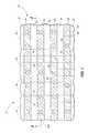
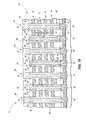
- FIG. 1is a diagrammatic top plan view of a substrate in accordance with an embodiment of the invention.
- FIG. 2is a diagrammatic cross sectional view taken through line 2 - 2 in FIG. 1 .
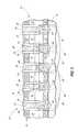
- FIG. 3is an enlargement of a portion of FIG. 2 .
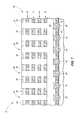
- FIG. 4is a diagrammatic sectional view of a substrate in process in accordance with an embodiment of the invention.
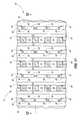
- FIG. 5is a diagrammatic top plan view of the substrate of FIG. 4 at a processing step subsequent to that shown by FIG. 4 .
- FIG. 6is a cross sectional view taken through line 6 - 6 in FIG. 5 .
- FIG. 7is a view of the FIG. 6 substrate at a processing step subsequent to that shown by FIGS. 5 and 6 .
- FIG. 8is a top view of the substrate of FIG. 7 at a processing step subsequent to that shown by FIG. 7 .
- FIG. 9is a cross sectional view taken through line 9 - 9 in FIG. 8 .
- FIG. 10is a view of the FIG. 9 substrate at a processing step subsequent to that shown by FIGS. 8 and 9 .
- FIG. 11is a top view of the substrate of FIG. 10 at a processing step subsequent to that shown by FIG. 10 .
- FIG. 12is a cross sectional view taken through line 12 - 12 in FIG. 11 .
- FIG. 13is a view of the FIG. 12 substrate at a processing step subsequent to that shown by FIGS. 11 and 12 .
- FIG. 14is a view of the FIG. 13 substrate at a processing step subsequent to that shown by FIG. 13 .
- FIG. 15is a view of the FIG. 14 substrate at a processing step subsequent to that shown by FIG. 14 .
- FIG. 16is a view of the FIG. 15 substrate at a processing step subsequent to that shown by FIG. 15 .
- FIG. 17is a view of the FIG. 16 substrate at a processing step subsequent to that shown by FIG. 16 .
- FIG. 18is a view of the FIG. 17 substrate at a processing step subsequent to that shown by FIG. 17 .
- FIG. 19is a view of the FIG. 18 substrate at a processing step subsequent to that shown by FIG. 18 .
- FIG. 20is a top view of the substrate of FIG. 19 at a processing step subsequent to that shown by FIG. 19 .
- FIG. 21is a cross sectional view taken through line 21 - 21 in FIG. 20 .
- Embodiments of the inventioninclude arrays of memory cells independent of method of fabrication, and methods of forming an array of vertically stacked tiers of memory cells.
- the memory cellsmay be nonvolatile.
- Initial example arraysare described with reference to FIGS. 1-3 and a substrate fragment 10 comprising a suitable base substrate 12 over which various materials have been provided.
- Base substrate 12may be homogenous or non-homogenous, for example comprising multiple different composition materials and/or layers.
- suchmay comprise bulk monocrystalline silicon and/or a semiconductor-on-insulator substrate.
- suchmay comprise dielectric material having conductive contacts or vias formed therein which extend vertically or otherwise into current conductive electrical connection with electronic device components, regions, or material elevationally inward of the dielectric material.
- verticalis a direction generally orthogonal to a primary surface relative to which the substrate is processed during fabrication and which may be considered to define a generally horizontal direction.
- vertical and horizontalas used herein are generally perpendicular directions relative one another independent of orientation of the substrate in three-dimensional space.
- elevational and “elevationally”are referenced to the vertical direction from a base substrate upon which the circuitry is fabricated.
- the base substratemay or may not be a semiconductor substrate.
- semiconductor substrateor “semiconductive substrate” is defined to mean any construction comprising semiconductive material, including, but not limited to, bulk semiconductive materials such as a semiconductive wafer (either alone or in assemblies comprising other materials thereon), and semiconductive material layers (either alone or in assemblies comprising other materials).
- substraterefers to any supporting structure, including, but not limited to, the semiconductive substrates described above.
- FIGS. 1-3show an array 14 of vertically stacked tiers 16 , 17 , 18 , 19 of memory cells 20 .
- Logic circuitry(not shown) may be fabricated outside of the array area.
- Control and/or other peripheral circuitry (not shown) for operating the memory arraymay or may not fully or partially be within the array area, with an example array area as a minimum encompassing all of the memory cells of a given array/sub-array.
- multiple sub-arraysmight also be fabricated and operated independently, in tandem, or otherwise relative one another.
- a “sub-array”may also be considered as an array.
- FIG. 2shows four vertically stacked tiers 16 - 19 of individual memory cells 20 .
- One or more tiersmay be elevationally outward of tier 16 and/or elevationally inward of tier 19 . Further, fewer than four tiers may be fabricated.
- Vertical tiers 16 - 19may be of the same or different respective construction(s). In one embodiment, all of such are of the same construction, for example to achieve an ultimate highest density and/or for ease in fabrication.
- Array 14includes a plurality of horizontally oriented access lines 22 (i.e., word lines) within the individual tiers of memory cells.
- Lines 22may comprise current conductive material, and may be homogenous or non-homogenous.
- current conductive materialis a composition wherein electric current flow would inherently occur therein predominantly by movement of sub-atomic positive and/or negative charges when such are generated as opposed to predominantly by movement of ions.
- Example current conductive materialsare elemental metals, alloys of elemental metals, current conductive metal compounds, and conductively doped semiconductive material, including any combinations thereof.
- a plurality of horizontally oriented global sense lines 24are elevationally outward of the tiers of memory cells.
- Sense lines 24may comprise current conductive material, and may be homogenous or non-homogenous. Such may be of the same or different composition as that of access lines 22 , with example materials being as described above.
- One or more dielectric materials 33may be provided between certain current conductive materials as shown.
- Array 10includes a plurality of pairs 32 ( FIG. 2 ) of local first vertical lines 34 and second vertical lines 36 extending through the tiers of memory cells.
- Local first vertical lines 34 within individual of pairs 32are in conductive connection with one of global sense lines 24 and in conductive connection with one of the two source/drain regions of one of the select transistors 26 .
- Local second vertical lines 36 within individual of pairs 32are in conductive connection with another of the two source/drain regions of the one select transistor 26 .
- Local first and second vertical lines 34 , 36may comprise current conductive material, and may be homogenous or non-homogenous. Such may be of the same or different composition(s), with the example current conductive materials described above being examples.
- Current conductive material 37may comprise local first and second vertical lines 34 , 36 , respectively, or otherwise be provided between local first and second vertical lines 34 , 36 and the source/drain regions 28 , 30 , respectively.
- local second vertical lines 36are laterally lined with programmable material 40 .
- programmable material 40may be solid, gel, amorphous, crystalline, or any other suitable phase. Any programmable material may be used, with only some examples being provided below.
- Suchmay have silver, copper, cobalt, and/or nickel ions, and/or other suitable ions, diffused therein for ionic conduction, analogously to structures disclosed in U.S. Pat. No. 7,405,967 and U.S. Patent Publication Number 2010/0193758.
- Additional example programmable materialsinclude multi-resistive state metal oxide-comprising material. Such may comprise, for example, at least two different layers or regions generally regarded as or understood to be active or passive regions, although not necessarily. Alternately, such may only comprise active material.
- Example active cell region compositions which comprise metal oxide and can be configured in multi-resistive statesinclude one or a combination of Sr x Ru y O z , Ru x O y , and In x Sn y O z .
- Example passive cell region compositionsinclude one or a combination of Al 2 O 3 , TiO 2 , and HfO 2 .
- a programmable material compositemight comprise additional metal oxide or other materials not comprising metal oxide.
- Example materials and constructions for a multi-resistive state region comprising one or more layers including a programmable metal oxide-comprising materialare described and disclosed in U.S. Pat.
- multi-resistive state metal oxide-comprising materialsencompass filament-type metal oxides, ferroelectric metal oxides and others as long as resistance of the metal oxide-comprising material can be selectively changed.
- the programmable materialmay comprise memristive material.
- such materialmay be statically programmable semiconductive material which comprises mobile dopants that are within a dielectric such that the material is statically programmable between at least two different resistance states. At least one of the states includes localization or gathering of the mobile dopants such that a dielectric region is formed and thereby provides a higher resistance state. Further, more than two programmable resistance states may be used.
- a “mobile dopant”is a component (other than a free electron) of the semiconductive material that is movable to different locations within said dielectric during normal device operation of repeatedly programming the device between at least two different static states by application of voltage differential to the pair of electrodes.
- Examplesinclude atom vacancies in an otherwise stoichiometric material, and atom interstitials.
- mobile dopantsinclude oxygen atom vacancies in amorphous or crystalline oxides or other oxygen-containing material, nitrogen atom vacancies in amorphous or crystalline nitrides or other nitrogen-containing material, fluorine atom vacancies in amorphous or crystalline fluorides or other fluorine-containing material, and interstitial metal atoms in amorphous or crystalline oxides. More than one type of mobile dopant may be used.
- Example dielectrics in which the mobile dopants are receivedinclude suitable oxides, nitrides, and/or fluorides that are capable of localized electrical conductivity based upon sufficiently high quantity and concentration of the mobile dopants.
- the dielectric within which the mobile dopants are receivedmay or may not be homogenous independent of consideration of the mobile dopants.
- Specific example dielectricsinclude TiO 2 , AlN, and/or MgF 2 .
- Example programmable materials that comprise oxygen vacancies as mobile dopantsmay comprise a combination of TiO 2 and TiO 2-x in at least one programmed resistance state depending on location of the oxygen vacancies and the quantity of the oxygen vacancies in the locations where such are received.
- An example programmable material that comprises nitrogen vacancies as mobile dopantsis a combination of MN and AlN 1-x in at least one programmed state depending on location of the nitrogen vacancies and the quantity of the nitrogen vacancies in the locations where such are received.
- An example programmable material that comprises fluorine vacancies as mobile dopantsmay is a combination of MgF 2 and MgF 2-x in at least one programmed resistance state depending on location of the fluorine vacancies and the quantity of the fluorine vacancies in the locations where such are received.
- the mobile dopantsmay comprise aluminum atom interstitials in a nitrogen-containing material.
- Still other example programmable materialsinclude polymer materials such as Bengala Rose, AlQ 3 Ag, Cu-TCNQ, DDQ, TAPA, and fluorescine-based polymers.
- Individual of memory cells 20comprise a crossing of local second vertical lines 36 and one of horizontal access lines 22 , and programmable material 40 there-between. While programmable material 40 is shown as being a continuous lining about local second vertical lines 36 , such may be discontinuous and/or only provided laterally between the respective horizontally oriented access lines 22 and local second vertical lines 36 in some embodiments.
- an array of vertically stacked tiers of memory cellscomprises a plurality of horizontally oriented access lines within individual tiers of memory cells.
- the arrayalso comprises a plurality of horizontally oriented global sense lines independent of whether such are elevationally outward of the tiers of memory cells. In one implementation, such global sense lines are elevationally outward of the tiers of memory cells.
- the arrayalso comprises a plurality of pairs of adjacent select transistors independent of whether such are elevationally inward of the tiers of memory cells. In one implementation, such select transistors are elevationally inward of the tiers of memory cells.
- FIGS. 1-3 embodimentan example of plurality of pairs 46 ( FIG. 3 ) of immediately adjacent select transistors 26 is shown.
- the pairsindividually comprise a shared mid-source drain region 30 and two laterally outer source/drain regions 28 .
- the array of such embodimentalso includes a plurality of alternating first and second local vertical lines independent of whether the local first vertical lines extend through the tiers of memory cells.
- the local first vertical linesextend through the tiers of memory cells. Regardless, the local first vertical lines are in conductive connection with one of the global sense lines and in conductive connection with one of the laterally outer source/drain regions.
- the local second vertical linesextend through the tiers of memory cells and are in conductive connection with one of the shared source/drain regions. Individual of the memory cells comprise a crossing of the local second vertical lines and one of the horizontal access lines, and include programmable material there-between.
- FIGS. 1-3 embodimentis but one example.
- the adjacent select transistors within an individual pair of select transistorsmay have their gates wired together in parallel. For example, such may be hard-wired together or soft-wired together.
- gatesare hard-wired together if a permanent conductive connection exists between such gates.
- Gatesare soft-wired together if no permanent conductive connection exists between such gates, but such may be selectively placed into conductive connection with one another via software control.
- the laterally outer source/drain regions and local first vertical linesare shared by immediately adjacent of such pairs of adjacent select transistors.
- FIGS. 1-3show but one example.
- An embodiment of the inventionencompasses an array of memory cells independent of whether such include vertically stacked tiers.
- the memory cellsare arranged in vertically stacked tiers.
- the arrayincludes a plurality of crossing access lines and sense lines. Programmable material is between the crossing access and sense lines.
- the arrayincludes two select transistors having respective gates that are wired in parallel to selectively enable current flow in each sense line.
- the access linesare arranged in vertically stacked tiers individually comprising a plurality of access lines.
- the sense linescomprise local lines within the array, and further comprise global lines within the array in switchable conductive connection with the local lines.
- second vertical lines 36 , first vertical lines 34 , and global lines 24 within array 10constitute example sense lines in switchable conductive connection via select transistors 26 .
- the global linesmay be elevationally outward of all of the access lines within the array.
- the select transistorsare elevationally inward of all the access lines within the array. Other attributes from the above first-described embodiments may be used.
- the below chartshows example relative voltages which may be used to write, read, and erase any given memory cell, specifically for the example depicted memory cell 20 n in FIG. 2 .
- embodiments of the inventionencompass methods of forming an array of vertically stacked tiers of memory cells, for example as is next-described with reference to FIGS. 4-21 .
- FIG. 4a substrate fragment 50 is shown, for example in fabricating array 14 of FIGS. 1-3 .
- Like numerals from FIGS. 1-3have been used where appropriate, with some construction differences being indicated with the suffix “a” or with different numerals. Further, numerals of the components shown in FIGS. 1-3 have been used to designate the materials from which such components are fabricated prior to the materials necessarily being of the final example shapes for clarity in the drawings and ease of understanding in the description.
- FIG. 4depicts select transistors 26 and alternating dielectric material 33 and access line material 22 formed thereover.
- An outer hardmask 38has been provided over outermost material 33 . Where, for example, material 33 comprises silicon dioxide, an example material 38 is silicon nitride. Regardless, materials 33 and 38 individually may be homogenous or non-homogenous.
- multiple tiers 16 , 17 , 18 and 19have been formed which individually comprise a plurality of horizontally oriented access lines 22 . Such may be formed, by way of example, by patterning and etch to form trenches 54 as shown. Innermost dielectric region 33 may comprise an outermost etch stop material (not shown) to provide an etch-stopping function when innermost material 22 has been etched through.
- trenches 54have been filled with dielectric material which has subsequently been planarized back at least to elevationally outermost surfaces of hardmask material 38 .
- the dielectric materialmay be homogenous or non-homogenous and, in one embodiment, may be of the same composition as that of material 33 and is so shown and designated in the figures.
- first and second local openings 56 , 58have been formed through tiers 16 - 19 between access lines 22 over individual of source/drain regions 28 , 30 .
- first local openings 56 and second local openings 58are formed using the same masking step.
- individual openings 56 , 58may be formed in a self-aligning manner in opposing lateral directions relative to immediately laterally adjacent of access lines 22 .
- mask lines(not shown) could be formed orthogonally relative to access lines 22 with trenches formed there-between which overlie the respective openings 56 , 58 .
- Removal (i.e., by etching) of dielectric material 33 deposited in FIG. 7may then occur selectively, and in one embodiment highly selectively, relative to the material of select lines 22 , thereby self-aligning relative to such lines.
- a “selective” etchrequires removal of the stated one material relative to another at a rate of at least 1.5:1, and a highly selective etch at a rate of at least about 10:1.
- a “self-aligning manner”means a technique whereby at least a lateral surface of a structure is defined by deposition of material against a sidewall of a previously patterned structure.
- first local openings 56 and second local openings 58have been lined with dielectric material.
- the same dielectric materiallines first local openings 56 and second local openings 58 , and in such embodiment may be deposited into the openings at the same time.
- the dielectric material lining openings 56 , 58may be homogenous or non-homogenous.
- the dielectric materialmay be of the same composition as that of hardmask material 38 and is so shown and designated in the figures. Regardless, hardmask material 38 may have been partially or wholly removed (not shown) earlier.
- a mask(not shown) has been formed over the substrate to cover material 38 within first openings 56 and to leave trench openings formed there-through over material 38 within second local openings 58 outwardly exposed.
- dielectric material 38 that was lining second local openings 58has been removed.
- all of dielectric material 38 that was lining second local openings 58has been removed.
- remaining volume of first openings 56may be considered as first openings 59 .
- processing through FIGS. 11 and 12may be considered as the forming of alternating first and second local openings 59 , 58 , respectively.
- second local openings 58have been lined with programmable material 40 .
- programmable material 40is deposited to less-than-fill second local openings 58 and to fill first local openings 59 .
- such acts of filling and lining with programmable material 40 relative to first local openings 59 and second local openings 58occur in the same deposition step.
- FIG. 13depicts but one example embodiment of replacing dielectric material 38 that was lining second local openings 58 with a programmable material lining 40 .
- programmable material 40has been anisotropically etched to remove such from horizontal surfaces. Such may expose conductive material 37 which may be in conductive connection with source/drain regions 30 .
- conductive material 36has been formed in second openings 58 in conductive connection with alternating source/drain regions 30 . Such may be formed by deposition of conductive material 36 to a sufficient thickness to fill remaining volume of second local openings 58 , followed by planarizing at least to the elevationally outermost surface of outer material 33 , as shown. Programmable material 40 in second local openings 58 is laterally between conductive material 36 and access lines 22 .
- dielectric materialhas been formed over and as part of substrate 50 .
- Suchmay be homogenous or non-homogenous and, in one embodiment, may be of the same composition as that of material 33 and is so shown and designated in the figures.
- substrate 50has been patterned to form contact openings 57 through material 33 over at least programmable material 40 within first local openings 56 , 59 and to leave such programmable material within second openings 58 masked.
- programmable material 40within first local openings 56 , 59 has been removed, for example by selective etching relative to materials 33 , 38 , and 37 .
- An anisotropic etchmay then be conducted of material 38 to expose conductive material 37 in the bottom of first openings 59 .
- conductive material 34has been formed in first local openings 56 in conductive connection with individual of source/drain regions 28 .
- Suchprovides but one example processing of replacing programmable material in first local openings 56 , 59 with conductive material (i.e., material 34 ) in conductive connection with individual of source/drain regions 28 .
- such replacingremoves all of programmable material 40 that was in first local openings 56 , 59 .
- Conductive material 34 within first local openings 56 , 59 and conductive material 36 in second local openings 58may be of the same or different composition(s).
- a plurality of horizontally oriented global sense lines 24have been provided elevationally outward of tiers 16 - 19 in conductive connection with conductive material 34 in first local openings 56 , 59 .
- Suchmay, by way of example only, be formed by deposition followed by patterning and subtractive etch.
- Material of global sense lines 24 and that of material 34may be of the same or different composition(s).
- lines 24 and conductive material 34may comprise the same material deposited and formed in a damascene-like manner in the same deposition step(s).
- FIGS. 20 and 21depict in one example an embodiment essentially the same as that depicted by FIGS. 1-3 .
- Embodiments of the inventionencompass methods of forming an array of vertically stacked tiers of memory cells comprising forming multiple tiers that individually comprise a plurality of horizontally oriented access lines.
- a plurality of select transistorsis provided elevationally inward of the tiers, with such individually comprising source/drain regions.
- alternating first and second local openingsare formed through the tiers between the access lines over individual of the source/drain regions in the same masking step.
- Conductive materialis formed in the first local openings in conductive connection with alternating ones of the source/drain regions.
- Laterally outer programmable material and laterally inner conductive materialare formed in the second local openings. The laterally inner conductive material is in conductive connection with alternating others of the source/drain regions.
- the conductive material in the first local openingsis formed after forming the laterally inner conductive material in the second local openings. In one embodiment, the conductive material in the first local openings is formed after forming the laterally outer programmable material in the second local openings.
- programmable materialis formed in the first local openings. In one example, such programmable material is formed in the first and second local openings in the same deposition step. In one example, the programmable material is removed from the first local openings, and in one example before forming the conductive material in the first local openings. In one example, all of the programmable material is removed from the first local openings.
- a plurality of horizontally oriented global sense linesis ultimately provided elevationally outward of the tiers in conductive connection with the conductive material in the first local openings.
- first and second local openingsare formed through the tiers between the access lines over individual of the source/drain regions independent of whether such are formed in the same masking step. In one embodiment, such may be formed in the same masking step.
- the first and second local openingsare lined with dielectric material.
- the dielectric material that is lining the second local openingsis replaced with a programmable material lining.
- Conductive materialis formed in the first and second local openings in conductive connection with individual of the source/drain regions, with the programmable material in the second local openings being laterally between the current conductive material and the access lines.
- a plurality of horizontally oriented global sense linesare ultimately provided elevationally outward of the tiers in conductive connection with the conductive material in the first local openings. Other attributes as shown and/or described above may be used.
- a method of forming an array of vertically stacked tiers of memory cellsforms alternating first and second local openings through the tiers between the access lines over individual of the source/drain regions independent of whether such occurs in the same masking step. In one embodiment, such does occur in the same masking step. Regardless, the first local openings are filled with programmable material and the second local openings are less-than-filled with programmable material regardless of whether such occurs in the same deposition step. In one embodiment, such occurs in the same deposition step. Conductive material is formed in the second local openings in conductive connection with individual of the source/drain regions. The programmable material in the second local openings is laterally between the current conductive material and the access lines.
- the programmable material in the first local openingsis replaced with current conductive material in conductive connection with individual of the source/drain regions.
- a plurality of horizontally oriented global sense linesis provided elevationally outward of the tiers in conductive connection with the conductive material in the first local openings.
- Other attributes as described and/or shown abovemay be used.
Landscapes
- Engineering & Computer Science (AREA)
- Manufacturing & Machinery (AREA)
- Semiconductor Memories (AREA)
Abstract
Description
| Line | 22n | |||
| WRITE | 3 V | 5 V | 0 V | ||
| READ | 1 V | 3 V | 0 V | ||
| ERASE | 0 V | 3 V | 3 V | ||
Claims (8)
Priority Applications (4)
| Application Number | Priority Date | Filing Date | Title |
|---|---|---|---|
| US13/074,642US8933491B2 (en) | 2011-03-29 | 2011-03-29 | Arrays of memory cells and methods of forming an array of vertically stacked tiers of memory cells |
| US14/594,813US10256275B2 (en) | 2011-03-29 | 2015-01-12 | Arrays of memory cells and methods of forming an array of vertically stacked tiers of memory cells |
| US16/283,645US11276733B2 (en) | 2011-03-29 | 2019-02-22 | Arrays of memory cells and methods of forming an array of vertically stacked tiers of memory cells |
| US17/589,683US12167615B2 (en) | 2011-03-29 | 2022-01-31 | Arrays of memory cells and methods of forming an array of vertically stacked tiers of memory cells |
Applications Claiming Priority (1)
| Application Number | Priority Date | Filing Date | Title |
|---|---|---|---|
| US13/074,642US8933491B2 (en) | 2011-03-29 | 2011-03-29 | Arrays of memory cells and methods of forming an array of vertically stacked tiers of memory cells |
Related Child Applications (1)
| Application Number | Title | Priority Date | Filing Date |
|---|---|---|---|
| US14/594,813DivisionUS10256275B2 (en) | 2011-03-29 | 2015-01-12 | Arrays of memory cells and methods of forming an array of vertically stacked tiers of memory cells |
Publications (2)
| Publication Number | Publication Date |
|---|---|
| US20120248504A1 US20120248504A1 (en) | 2012-10-04 |
| US8933491B2true US8933491B2 (en) | 2015-01-13 |
Family
ID=46926059
Family Applications (4)
| Application Number | Title | Priority Date | Filing Date |
|---|---|---|---|
| US13/074,642Active2031-08-18US8933491B2 (en) | 2011-03-29 | 2011-03-29 | Arrays of memory cells and methods of forming an array of vertically stacked tiers of memory cells |
| US14/594,813Active2032-02-08US10256275B2 (en) | 2011-03-29 | 2015-01-12 | Arrays of memory cells and methods of forming an array of vertically stacked tiers of memory cells |
| US16/283,645ActiveUS11276733B2 (en) | 2011-03-29 | 2019-02-22 | Arrays of memory cells and methods of forming an array of vertically stacked tiers of memory cells |
| US17/589,683Active2032-06-10US12167615B2 (en) | 2011-03-29 | 2022-01-31 | Arrays of memory cells and methods of forming an array of vertically stacked tiers of memory cells |
Family Applications After (3)
| Application Number | Title | Priority Date | Filing Date |
|---|---|---|---|
| US14/594,813Active2032-02-08US10256275B2 (en) | 2011-03-29 | 2015-01-12 | Arrays of memory cells and methods of forming an array of vertically stacked tiers of memory cells |
| US16/283,645ActiveUS11276733B2 (en) | 2011-03-29 | 2019-02-22 | Arrays of memory cells and methods of forming an array of vertically stacked tiers of memory cells |
| US17/589,683Active2032-06-10US12167615B2 (en) | 2011-03-29 | 2022-01-31 | Arrays of memory cells and methods of forming an array of vertically stacked tiers of memory cells |
Country Status (1)
| Country | Link |
|---|---|
| US (4) | US8933491B2 (en) |
Cited By (2)
| Publication number | Priority date | Publication date | Assignee | Title |
|---|---|---|---|---|
| US10199498B2 (en) | 2016-02-10 | 2019-02-05 | Toshiba Memory Corporation | Semiconductor memory device |
| US20220181550A1 (en)* | 2019-03-04 | 2022-06-09 | International Business Machines Corporation | Stacked access device and resistive memory |
Families Citing this family (26)
| Publication number | Priority date | Publication date | Assignee | Title |
|---|---|---|---|---|
| US8937292B2 (en) | 2011-08-15 | 2015-01-20 | Unity Semiconductor Corporation | Vertical cross point arrays for ultra high density memory applications |
| US8416609B2 (en)* | 2010-02-15 | 2013-04-09 | Micron Technology, Inc. | Cross-point memory cells, non-volatile memory arrays, methods of reading a memory cell, methods of programming a memory cell, methods of writing to and reading from a memory cell, and computer systems |
| US8409960B2 (en)* | 2011-04-08 | 2013-04-02 | Micron Technology, Inc. | Methods of patterning platinum-containing material |
| US8994489B2 (en) | 2011-10-19 | 2015-03-31 | Micron Technology, Inc. | Fuses, and methods of forming and using fuses |
| US9252188B2 (en) | 2011-11-17 | 2016-02-02 | Micron Technology, Inc. | Methods of forming memory cells |
| KR101912397B1 (en)* | 2011-11-25 | 2018-10-29 | 삼성전자주식회사 | Semiconductor memory device having three-dimensionally arranged resistive memory cells |
| US9136467B2 (en) | 2012-04-30 | 2015-09-15 | Micron Technology, Inc. | Phase change memory cells and methods of forming phase change memory cells |
| US9553262B2 (en) | 2013-02-07 | 2017-01-24 | Micron Technology, Inc. | Arrays of memory cells and methods of forming an array of memory cells |
| EP2887396B1 (en) | 2013-12-20 | 2017-03-08 | Imec | Three-dimensional resistive memory array |
| US9881971B2 (en) | 2014-04-01 | 2018-01-30 | Micron Technology, Inc. | Memory arrays |
| US9362494B2 (en) | 2014-06-02 | 2016-06-07 | Micron Technology, Inc. | Array of cross point memory cells and methods of forming an array of cross point memory cells |
| US9343506B2 (en)* | 2014-06-04 | 2016-05-17 | Micron Technology, Inc. | Memory arrays with polygonal memory cells having specific sidewall orientations |
| WO2016043657A1 (en)* | 2014-09-15 | 2016-03-24 | Agency For Science, Technology And Research | Memory structure, method for fabricating thereof, memory array device and method for operating thereof |
| US9761580B1 (en) | 2016-11-01 | 2017-09-12 | Micron Technology, Inc. | Methods of forming an array comprising pairs of vertically opposed capacitors and arrays comprising pairs of vertically opposed capacitors |
| US10014305B2 (en) | 2016-11-01 | 2018-07-03 | Micron Technology, Inc. | Methods of forming an array comprising pairs of vertically opposed capacitors and arrays comprising pairs of vertically opposed capacitors |
| US10062745B2 (en) | 2017-01-09 | 2018-08-28 | Micron Technology, Inc. | Methods of forming an array of capacitors, methods of forming an array of memory cells individually comprising a capacitor and a transistor, arrays of capacitors, and arrays of memory cells individually comprising a capacitor and a transistor |
| US9837420B1 (en) | 2017-01-10 | 2017-12-05 | Micron Technology, Inc. | Arrays of memory cells individually comprising a capacitor and an elevationally-extending transistor, methods of forming a tier of an array of memory cells, and methods of forming an array of memory cells individually comprising a capacitor and an elevationally-extending transistor |
| US9842839B1 (en) | 2017-01-12 | 2017-12-12 | Micron Technology, Inc. | Memory cell, an array of memory cells individually comprising a capacitor and a transistor with the array comprising rows of access lines and columns of digit lines, a 2T-1C memory cell, and methods of forming an array of capacitors and access transistors there-above |
| US10236301B1 (en)* | 2017-12-27 | 2019-03-19 | Micron Technology, Inc. | Methods of forming an array of elevationally-extending strings of memory cells |
| US10388658B1 (en) | 2018-04-27 | 2019-08-20 | Micron Technology, Inc. | Transistors, arrays of transistors, arrays of memory cells individually comprising a capacitor and an elevationally-extending transistor, and methods of forming an array of transistors |
| CN112635661B (en)* | 2019-10-09 | 2023-08-01 | 联华电子股份有限公司 | Multi-bit variable resistance memory cell and method for forming same |
| CN112687717B (en)* | 2019-10-18 | 2024-03-08 | 华邦电子股份有限公司 | Variable resistance memory and manufacturing method thereof |
| US11177321B2 (en)* | 2019-10-23 | 2021-11-16 | Winbond Electronics Corp. | Resistive random access memories and method for fabricating the same |
| US11462686B2 (en) | 2020-06-22 | 2022-10-04 | Nantero, Inc. | Three-dimensional array architecture for resistive change element arrays and methods for making same |
| US12029049B2 (en)* | 2020-12-16 | 2024-07-02 | Winbond Electronics Corp. | Memory structures and methods for forming the same |
| CN114665009B (en)* | 2020-12-22 | 2025-06-10 | 华邦电子股份有限公司 | Memory structure and manufacturing method thereof |
Citations (13)
| Publication number | Priority date | Publication date | Assignee | Title |
|---|---|---|---|---|
| US5206183A (en) | 1992-02-19 | 1993-04-27 | Micron Technology, Inc. | Method of forming a bit line over capacitor array of memory cells |
| US20010053575A1 (en) | 1998-12-03 | 2001-12-20 | Wendell P. Noble | Trench dram cell with vertical device and buried word lines |
| US20040151024A1 (en)* | 2003-02-05 | 2004-08-05 | Peter Fricke | Memory array |
| US20070018630A1 (en)* | 2004-01-14 | 2007-01-25 | Jurgen Oehm | Transistor arrangement with temperature compensation and method for temperature compensation |
| US20080123392A1 (en)* | 2005-06-20 | 2008-05-29 | Fujitsu Limited | Nonvolatile semiconductor memory device and method of writing into the same |
| US20080310209A1 (en) | 2007-06-14 | 2008-12-18 | Micron Technology, Inc. | Circuit, biasing scheme and fabrication method for diode accesed cross-point resistive memory array |
| US20090168495A1 (en)* | 2006-09-05 | 2009-07-02 | Fujitsu Limited | Semiconductor memory device and method of writing into semiconductor memory device |
| US20100008124A1 (en) | 2008-07-09 | 2010-01-14 | Sandisk 3D Llc | Cross point memory cell with distributed diodes and method of making same |
| US20100052030A1 (en)* | 2008-08-29 | 2010-03-04 | Takeshi Sakaguchi | Nonvolatile semiconductor memory and manufacturing method thereof |
| US20100188894A1 (en)* | 2009-01-29 | 2010-07-29 | Qualcomm Incorporated | In-situ resistance measurement for magnetic random access memory (mram) |
| US7838360B2 (en) | 2005-05-13 | 2010-11-23 | Micron Technology, Inc. | Memory array with surrounding gate access transistors and capacitors with global and staggered local bit lines |
| US20100295134A1 (en) | 2009-05-20 | 2010-11-25 | Satoshi Nagashima | Semiconductor memory device and method of fabricating the same |
| US20110216603A1 (en)* | 2010-03-04 | 2011-09-08 | Samsung Electronics Co., Ltd. | Non-Volatile Memory Device, Erasing Method Thereof, And Memory System Including The Same |
Family Cites Families (14)
| Publication number | Priority date | Publication date | Assignee | Title |
|---|---|---|---|---|
| US5068603A (en)* | 1987-10-07 | 1991-11-26 | Xilinx, Inc. | Structure and method for producing mask-programmed integrated circuits which are pin compatible substitutes for memory-configured logic arrays |
| US6737696B1 (en) | 1998-06-03 | 2004-05-18 | Micron Technology, Inc. | DRAM capacitor formulation using a double-sided electrode |
| US7791141B2 (en)* | 2004-07-09 | 2010-09-07 | International Business Machines Corporation | Field-enhanced programmable resistance memory cell |
| JP2008277543A (en)* | 2007-04-27 | 2008-11-13 | Toshiba Corp | Nonvolatile semiconductor memory device |
| US8338812B2 (en)* | 2008-01-16 | 2012-12-25 | Micron Technology, Inc. | Vertical spacer electrodes for variable-resistance material memories and vertical spacer variable-resistance material memory cells |
| KR101418434B1 (en)* | 2008-03-13 | 2014-08-14 | 삼성전자주식회사 | Non-volatile memory device, method of fabricating the same, and processing system comprising the same |
| US8134865B2 (en)* | 2008-05-06 | 2012-03-13 | Macronix International Co., Ltd. | Operating method of electrical pulse voltage for RRAM application |
| KR20090126676A (en)* | 2008-06-05 | 2009-12-09 | 주식회사 하이닉스반도체 | Resistive RAM device and manufacturing method thereof |
| JP2010003916A (en)* | 2008-06-20 | 2010-01-07 | Elpida Memory Inc | Semiconductor device and method of manufacturing the same |
| KR20100032572A (en)* | 2008-09-18 | 2010-03-26 | 주식회사 하이닉스반도체 | Resistive memory device and method for manufacturing the same |
| KR101502584B1 (en)* | 2008-10-16 | 2015-03-17 | 삼성전자주식회사 | Nonvolatile memory device |
| JP4940260B2 (en)* | 2009-03-18 | 2012-05-30 | 株式会社東芝 | Resistance change type memory device |
| US8173987B2 (en)* | 2009-04-27 | 2012-05-08 | Macronix International Co., Ltd. | Integrated circuit 3D phase change memory array and manufacturing method |
| US20120086054A1 (en)* | 2010-10-12 | 2012-04-12 | Tzyy-Ming Cheng | Semiconductor structure and method for making the same |
- 2011
- 2011-03-29USUS13/074,642patent/US8933491B2/enactiveActive
- 2015
- 2015-01-12USUS14/594,813patent/US10256275B2/enactiveActive
- 2019
- 2019-02-22USUS16/283,645patent/US11276733B2/enactiveActive
- 2022
- 2022-01-31USUS17/589,683patent/US12167615B2/enactiveActive
Patent Citations (13)
| Publication number | Priority date | Publication date | Assignee | Title |
|---|---|---|---|---|
| US5206183A (en) | 1992-02-19 | 1993-04-27 | Micron Technology, Inc. | Method of forming a bit line over capacitor array of memory cells |
| US20010053575A1 (en) | 1998-12-03 | 2001-12-20 | Wendell P. Noble | Trench dram cell with vertical device and buried word lines |
| US20040151024A1 (en)* | 2003-02-05 | 2004-08-05 | Peter Fricke | Memory array |
| US20070018630A1 (en)* | 2004-01-14 | 2007-01-25 | Jurgen Oehm | Transistor arrangement with temperature compensation and method for temperature compensation |
| US7838360B2 (en) | 2005-05-13 | 2010-11-23 | Micron Technology, Inc. | Memory array with surrounding gate access transistors and capacitors with global and staggered local bit lines |
| US20080123392A1 (en)* | 2005-06-20 | 2008-05-29 | Fujitsu Limited | Nonvolatile semiconductor memory device and method of writing into the same |
| US20090168495A1 (en)* | 2006-09-05 | 2009-07-02 | Fujitsu Limited | Semiconductor memory device and method of writing into semiconductor memory device |
| US20080310209A1 (en) | 2007-06-14 | 2008-12-18 | Micron Technology, Inc. | Circuit, biasing scheme and fabrication method for diode accesed cross-point resistive memory array |
| US20100008124A1 (en) | 2008-07-09 | 2010-01-14 | Sandisk 3D Llc | Cross point memory cell with distributed diodes and method of making same |
| US20100052030A1 (en)* | 2008-08-29 | 2010-03-04 | Takeshi Sakaguchi | Nonvolatile semiconductor memory and manufacturing method thereof |
| US20100188894A1 (en)* | 2009-01-29 | 2010-07-29 | Qualcomm Incorporated | In-situ resistance measurement for magnetic random access memory (mram) |
| US20100295134A1 (en) | 2009-05-20 | 2010-11-25 | Satoshi Nagashima | Semiconductor memory device and method of fabricating the same |
| US20110216603A1 (en)* | 2010-03-04 | 2011-09-08 | Samsung Electronics Co., Ltd. | Non-Volatile Memory Device, Erasing Method Thereof, And Memory System Including The Same |
Non-Patent Citations (1)
| Title |
|---|
| Yoon, "Vertical Cross-Point Resistance Change Memory for Ultra-High Density Non-Volatile Memory Applications", VLSI Technology, 2009. |
Cited By (3)
| Publication number | Priority date | Publication date | Assignee | Title |
|---|---|---|---|---|
| US10199498B2 (en) | 2016-02-10 | 2019-02-05 | Toshiba Memory Corporation | Semiconductor memory device |
| US20220181550A1 (en)* | 2019-03-04 | 2022-06-09 | International Business Machines Corporation | Stacked access device and resistive memory |
| US12284922B2 (en)* | 2019-03-04 | 2025-04-22 | International Business Machines Corporation | Stacked access device and resistive memory |
Also Published As
| Publication number | Publication date |
|---|---|
| US20220157888A1 (en) | 2022-05-19 |
| US12167615B2 (en) | 2024-12-10 |
| US10256275B2 (en) | 2019-04-09 |
| US20190189689A1 (en) | 2019-06-20 |
| US20120248504A1 (en) | 2012-10-04 |
| US20150123070A1 (en) | 2015-05-07 |
| US11276733B2 (en) | 2022-03-15 |
Similar Documents
| Publication | Publication Date | Title |
|---|---|---|
| US12167615B2 (en) | Arrays of memory cells and methods of forming an array of vertically stacked tiers of memory cells | |
| US12406919B2 (en) | Stack of horizontally extending and vertically overlapping features, methods of forming circuitry components, and methods of forming an array of memory cells | |
| US8791447B2 (en) | Arrays of nonvolatile memory cells and methods of forming arrays of nonvolatile memory cells | |
| US8796661B2 (en) | Nonvolatile memory cells and methods of forming nonvolatile memory cell | |
| US9620174B2 (en) | Arrays of nonvolatile memory cells comprising a repetition of a unit cell, arrays of nonvolatile memory cells comprising a combination of vertically oriented and horizontally oriented memory cells, and arrays of vertically stacked tiers of nonvolatile memory cells | |
| US8431458B2 (en) | Methods of forming a nonvolatile memory cell and methods of forming an array of nonvolatile memory cells |
Legal Events
| Date | Code | Title | Description |
|---|---|---|---|
| AS | Assignment | Owner name:MICRON TECHNOLOGY, INC., IDAHO Free format text:ASSIGNMENT OF ASSIGNORS INTEREST;ASSIGNOR:LIU, ZENGTAO T.;REEL/FRAME:026044/0643 Effective date:20110328 Owner name:MICRON TECHNOLOGY, INC., IDAHO Free format text:ASSIGNMENT OF ASSIGNORS INTEREST;ASSIGNOR:LIU, ZENGTAO T.;REEL/FRAME:026043/0083 Effective date:20110328 | |
| FEPP | Fee payment procedure | Free format text:PAYOR NUMBER ASSIGNED (ORIGINAL EVENT CODE: ASPN); ENTITY STATUS OF PATENT OWNER: LARGE ENTITY | |
| STCF | Information on status: patent grant | Free format text:PATENTED CASE | |
| CC | Certificate of correction | ||
| AS | Assignment | Owner name:U.S. BANK NATIONAL ASSOCIATION, AS COLLATERAL AGENT, CALIFORNIA Free format text:SECURITY INTEREST;ASSIGNOR:MICRON TECHNOLOGY, INC.;REEL/FRAME:038669/0001 Effective date:20160426 Owner name:U.S. BANK NATIONAL ASSOCIATION, AS COLLATERAL AGEN Free format text:SECURITY INTEREST;ASSIGNOR:MICRON TECHNOLOGY, INC.;REEL/FRAME:038669/0001 Effective date:20160426 | |
| AS | Assignment | Owner name:MORGAN STANLEY SENIOR FUNDING, INC., AS COLLATERAL AGENT, MARYLAND Free format text:PATENT SECURITY AGREEMENT;ASSIGNOR:MICRON TECHNOLOGY, INC.;REEL/FRAME:038954/0001 Effective date:20160426 Owner name:MORGAN STANLEY SENIOR FUNDING, INC., AS COLLATERAL Free format text:PATENT SECURITY AGREEMENT;ASSIGNOR:MICRON TECHNOLOGY, INC.;REEL/FRAME:038954/0001 Effective date:20160426 | |
| AS | Assignment | Owner name:U.S. BANK NATIONAL ASSOCIATION, AS COLLATERAL AGENT, CALIFORNIA Free format text:CORRECTIVE ASSIGNMENT TO CORRECT THE REPLACE ERRONEOUSLY FILED PATENT #7358718 WITH THE CORRECT PATENT #7358178 PREVIOUSLY RECORDED ON REEL 038669 FRAME 0001. ASSIGNOR(S) HEREBY CONFIRMS THE SECURITY INTEREST;ASSIGNOR:MICRON TECHNOLOGY, INC.;REEL/FRAME:043079/0001 Effective date:20160426 Owner name:U.S. BANK NATIONAL ASSOCIATION, AS COLLATERAL AGEN Free format text:CORRECTIVE ASSIGNMENT TO CORRECT THE REPLACE ERRONEOUSLY FILED PATENT #7358718 WITH THE CORRECT PATENT #7358178 PREVIOUSLY RECORDED ON REEL 038669 FRAME 0001. ASSIGNOR(S) HEREBY CONFIRMS THE SECURITY INTEREST;ASSIGNOR:MICRON TECHNOLOGY, INC.;REEL/FRAME:043079/0001 Effective date:20160426 | |
| MAFP | Maintenance fee payment | Free format text:PAYMENT OF MAINTENANCE FEE, 4TH YEAR, LARGE ENTITY (ORIGINAL EVENT CODE: M1551) Year of fee payment:4 | |
| AS | Assignment | Owner name:JPMORGAN CHASE BANK, N.A., AS COLLATERAL AGENT, ILLINOIS Free format text:SECURITY INTEREST;ASSIGNORS:MICRON TECHNOLOGY, INC.;MICRON SEMICONDUCTOR PRODUCTS, INC.;REEL/FRAME:047540/0001 Effective date:20180703 Owner name:JPMORGAN CHASE BANK, N.A., AS COLLATERAL AGENT, IL Free format text:SECURITY INTEREST;ASSIGNORS:MICRON TECHNOLOGY, INC.;MICRON SEMICONDUCTOR PRODUCTS, INC.;REEL/FRAME:047540/0001 Effective date:20180703 | |
| AS | Assignment | Owner name:MICRON TECHNOLOGY, INC., IDAHO Free format text:RELEASE BY SECURED PARTY;ASSIGNOR:U.S. BANK NATIONAL ASSOCIATION, AS COLLATERAL AGENT;REEL/FRAME:047243/0001 Effective date:20180629 | |
| AS | Assignment | Owner name:MICRON TECHNOLOGY, INC., IDAHO Free format text:RELEASE BY SECURED PARTY;ASSIGNOR:MORGAN STANLEY SENIOR FUNDING, INC., AS COLLATERAL AGENT;REEL/FRAME:050937/0001 Effective date:20190731 | |
| AS | Assignment | Owner name:MICRON TECHNOLOGY, INC., IDAHO Free format text:RELEASE BY SECURED PARTY;ASSIGNOR:JPMORGAN CHASE BANK, N.A., AS COLLATERAL AGENT;REEL/FRAME:051028/0001 Effective date:20190731 Owner name:MICRON SEMICONDUCTOR PRODUCTS, INC., IDAHO Free format text:RELEASE BY SECURED PARTY;ASSIGNOR:JPMORGAN CHASE BANK, N.A., AS COLLATERAL AGENT;REEL/FRAME:051028/0001 Effective date:20190731 | |
| MAFP | Maintenance fee payment | Free format text:PAYMENT OF MAINTENANCE FEE, 8TH YEAR, LARGE ENTITY (ORIGINAL EVENT CODE: M1552); ENTITY STATUS OF PATENT OWNER: LARGE ENTITY Year of fee payment:8 |