US8932960B2 - Methods for isolating portions of a loop of pitch-multiplied material and related structures - Google Patents
Methods for isolating portions of a loop of pitch-multiplied material and related structuresDownload PDFInfo
- Publication number
- US8932960B2 US8932960B2US13/777,803US201313777803AUS8932960B2US 8932960 B2US8932960 B2US 8932960B2US 201313777803 AUS201313777803 AUS 201313777803AUS 8932960 B2US8932960 B2US 8932960B2
- Authority
- US
- United States
- Prior art keywords
- lines
- layer
- spacers
- semiconductor
- pattern
- Prior art date
- Legal status (The legal status is an assumption and is not a legal conclusion. Google has not performed a legal analysis and makes no representation as to the accuracy of the status listed.)
- Active
Links
- 239000000463materialSubstances0.000titleclaimsabstractdescription131
- 238000000034methodMethods0.000titleclaimsabstractdescription68
- 125000006850spacer groupChemical group0.000claimsabstractdescription73
- 239000004065semiconductorSubstances0.000claimsabstractdescription56
- 230000008569processEffects0.000claimsabstractdescription38
- 230000000873masking effectEffects0.000claimsabstractdescription26
- 239000000758substrateSubstances0.000claimsdescription49
- 229920002120photoresistant polymerPolymers0.000claimsdescription44
- 230000015654memoryEffects0.000claimsdescription40
- 238000000151depositionMethods0.000claimsdescription15
- 238000000059patterningMethods0.000claimsdescription12
- 229910003481amorphous carbonInorganic materials0.000claimsdescription10
- 238000005530etchingMethods0.000claimsdescription8
- 238000009966trimmingMethods0.000claims1
- 239000011295pitchSubstances0.000description51
- 210000004027cellAnatomy0.000description25
- 238000002955isolationMethods0.000description25
- 238000000206photolithographyMethods0.000description16
- 229910052814silicon oxideInorganic materials0.000description9
- 230000015572biosynthetic processEffects0.000description8
- VYPSYNLAJGMNEJ-UHFFFAOYSA-NSilicium dioxideChemical compoundO=[Si]=OVYPSYNLAJGMNEJ-UHFFFAOYSA-N0.000description7
- 239000006117anti-reflective coatingSubstances0.000description7
- 229910052710siliconInorganic materials0.000description7
- 239000010703siliconSubstances0.000description7
- XUIMIQQOPSSXEZ-UHFFFAOYSA-NSiliconChemical compound[Si]XUIMIQQOPSSXEZ-UHFFFAOYSA-N0.000description6
- 230000008021depositionEffects0.000description6
- 238000004519manufacturing processMethods0.000description6
- 238000012546transferMethods0.000description6
- 230000008901benefitEffects0.000description4
- 239000003990capacitorSubstances0.000description4
- -1i.e.Polymers0.000description4
- 230000001681protective effectEffects0.000description4
- 238000003491arrayMethods0.000description3
- QVGXLLKOCUKJST-UHFFFAOYSA-Natomic oxygenChemical compound[O]QVGXLLKOCUKJST-UHFFFAOYSA-N0.000description3
- 230000008859changeEffects0.000description3
- 230000003247decreasing effectEffects0.000description3
- 238000011049fillingMethods0.000description3
- 238000012986modificationMethods0.000description3
- 230000004048modificationEffects0.000description3
- 150000004767nitridesChemical class0.000description3
- 239000001301oxygenSubstances0.000description3
- 229910052760oxygenInorganic materials0.000description3
- 238000012545processingMethods0.000description3
- 238000005549size reductionMethods0.000description3
- 206010001513AIDS related complexDiseases0.000description2
- IJGRMHOSHXDMSA-UHFFFAOYSA-NAtomic nitrogenChemical compoundN#NIJGRMHOSHXDMSA-UHFFFAOYSA-N0.000description2
- KAKZBPTYRLMSJV-UHFFFAOYSA-NButadieneChemical compoundC=CC=CKAKZBPTYRLMSJV-UHFFFAOYSA-N0.000description2
- ATUOYWHBWRKTHZ-UHFFFAOYSA-NPropaneChemical compoundCCCATUOYWHBWRKTHZ-UHFFFAOYSA-N0.000description2
- 210000002945adventitial reticular cellAnatomy0.000description2
- 238000000231atomic layer depositionMethods0.000description2
- 239000007833carbon precursorSubstances0.000description2
- 238000005229chemical vapour depositionMethods0.000description2
- 238000010586diagramMethods0.000description2
- 239000002019doping agentSubstances0.000description2
- 230000005669field effectEffects0.000description2
- 230000006870functionEffects0.000description2
- 239000011810insulating materialSubstances0.000description2
- 239000012212insulatorSubstances0.000description2
- 238000001459lithographyMethods0.000description2
- 239000000203mixtureSubstances0.000description2
- 229910021420polycrystalline siliconInorganic materials0.000description2
- 229920005591polysiliconPolymers0.000description2
- 239000002243precursorSubstances0.000description2
- 230000005855radiationEffects0.000description2
- 230000009467reductionEffects0.000description2
- 230000002829reductive effectEffects0.000description2
- 238000003860storageMethods0.000description2
- OKTJSMMVPCPJKN-UHFFFAOYSA-NCarbonChemical compound[C]OKTJSMMVPCPJKN-UHFFFAOYSA-N0.000description1
- 229910052581Si3N4Inorganic materials0.000description1
- BOTDANWDWHJENH-UHFFFAOYSA-NTetraethyl orthosilicateChemical compoundCCO[Si](OCC)(OCC)OCCBOTDANWDWHJENH-UHFFFAOYSA-N0.000description1
- VZPPHXVFMVZRTE-UHFFFAOYSA-N[Kr]FChemical compound[Kr]FVZPPHXVFMVZRTE-UHFFFAOYSA-N0.000description1
- FAQXXMTVCNQJPT-UHFFFAOYSA-N[Si].Cl[Si](Cl)(Cl)[Si](Cl)(Cl)ClChemical compound[Si].Cl[Si](Cl)(Cl)[Si](Cl)(Cl)ClFAQXXMTVCNQJPT-UHFFFAOYSA-N0.000description1
- 238000007792additionMethods0.000description1
- ISQINHMJILFLAQ-UHFFFAOYSA-Nargon hydrofluorideChemical compoundF.[Ar]ISQINHMJILFLAQ-UHFFFAOYSA-N0.000description1
- 239000001273butaneSubstances0.000description1
- 229910052799carbonInorganic materials0.000description1
- 239000003575carbonaceous materialSubstances0.000description1
- 239000002131composite materialSubstances0.000description1
- 150000001875compoundsChemical class0.000description1
- 239000004020conductorSubstances0.000description1
- 239000000470constituentSubstances0.000description1
- 230000001276controlling effectEffects0.000description1
- 238000013500data storageMethods0.000description1
- 238000011161developmentMethods0.000description1
- 230000003292diminished effectEffects0.000description1
- 238000010894electron beam technologyMethods0.000description1
- 150000002430hydrocarbonsChemical class0.000description1
- 238000007654immersionMethods0.000description1
- 229910010272inorganic materialInorganic materials0.000description1
- 239000011147inorganic materialSubstances0.000description1
- IJDNQMDRQITEOD-UHFFFAOYSA-Nn-butaneChemical compoundCCCCIJDNQMDRQITEOD-UHFFFAOYSA-N0.000description1
- OFBQJSOFQDEBGM-UHFFFAOYSA-Nn-pentaneNatural productsCCCCCOFBQJSOFQDEBGM-UHFFFAOYSA-N0.000description1
- 238000001127nanoimprint lithographyMethods0.000description1
- 229910052757nitrogenInorganic materials0.000description1
- 230000002093peripheral effectEffects0.000description1
- 239000001294propaneSubstances0.000description1
- QQONPFPTGQHPMA-UHFFFAOYSA-NpropyleneNatural productsCC=CQQONPFPTGQHPMA-UHFFFAOYSA-N0.000description1
- 125000004805propylene groupChemical group[H]C([H])([H])C([H])([*:1])C([H])([H])[*:2]0.000description1
- MWWATHDPGQKSAR-UHFFFAOYSA-NpropyneChemical compoundCC#CMWWATHDPGQKSAR-UHFFFAOYSA-N0.000description1
- 230000001105regulatory effectEffects0.000description1
- 230000003252repetitive effectEffects0.000description1
- 230000000717retained effectEffects0.000description1
- 229910021332silicideInorganic materials0.000description1
- FVBUAEGBCNSCDD-UHFFFAOYSA-Nsilicide(4-)Chemical compound[Si-4]FVBUAEGBCNSCDD-UHFFFAOYSA-N0.000description1
- LIVNPJMFVYWSIS-UHFFFAOYSA-Nsilicon monoxideChemical class[Si-]#[O+]LIVNPJMFVYWSIS-UHFFFAOYSA-N0.000description1
- HQVNEWCFYHHQES-UHFFFAOYSA-Nsilicon nitrideChemical compoundN12[Si]34N5[Si]62N3[Si]51N64HQVNEWCFYHHQES-UHFFFAOYSA-N0.000description1
- 239000012686silicon precursorSubstances0.000description1
- 239000007787solidSubstances0.000description1
- 230000003068static effectEffects0.000description1
- 125000000383tetramethylene groupChemical group[H]C([H])([*:1])C([H])([H])C([H])([H])C([H])([H])[*:2]0.000description1
- 230000003685thermal hair damageEffects0.000description1
- LXEXBJXDGVGRAR-UHFFFAOYSA-Ntrichloro(trichlorosilyl)silaneChemical compoundCl[Si](Cl)(Cl)[Si](Cl)(Cl)ClLXEXBJXDGVGRAR-UHFFFAOYSA-N0.000description1
- 239000011800void materialSubstances0.000description1
Images


Classifications
- H—ELECTRICITY
- H01—ELECTRIC ELEMENTS
- H01L—SEMICONDUCTOR DEVICES NOT COVERED BY CLASS H10
- H01L21/00—Processes or apparatus adapted for the manufacture or treatment of semiconductor or solid state devices or of parts thereof
- H01L21/70—Manufacture or treatment of devices consisting of a plurality of solid state components formed in or on a common substrate or of parts thereof; Manufacture of integrated circuit devices or of parts thereof
- H01L21/71—Manufacture of specific parts of devices defined in group H01L21/70
- H01L21/768—Applying interconnections to be used for carrying current between separate components within a device comprising conductors and dielectrics
- H01L21/76801—Applying interconnections to be used for carrying current between separate components within a device comprising conductors and dielectrics characterised by the formation and the after-treatment of the dielectrics, e.g. smoothing
- H01L21/76802—Applying interconnections to be used for carrying current between separate components within a device comprising conductors and dielectrics characterised by the formation and the after-treatment of the dielectrics, e.g. smoothing by forming openings in dielectrics
- H01L21/76816—Aspects relating to the layout of the pattern or to the size of vias or trenches
- H01L29/66825—
- H—ELECTRICITY
- H01—ELECTRIC ELEMENTS
- H01L—SEMICONDUCTOR DEVICES NOT COVERED BY CLASS H10
- H01L21/00—Processes or apparatus adapted for the manufacture or treatment of semiconductor or solid state devices or of parts thereof
- H01L21/02—Manufacture or treatment of semiconductor devices or of parts thereof
- H01L21/02104—Forming layers
- H01L21/02365—Forming inorganic semiconducting materials on a substrate
- H01L21/02518—Deposited layers
- H—ELECTRICITY
- H01—ELECTRIC ELEMENTS
- H01L—SEMICONDUCTOR DEVICES NOT COVERED BY CLASS H10
- H01L21/00—Processes or apparatus adapted for the manufacture or treatment of semiconductor or solid state devices or of parts thereof
- H01L21/02—Manufacture or treatment of semiconductor devices or of parts thereof
- H01L21/027—Making masks on semiconductor bodies for further photolithographic processing not provided for in group H01L21/18 or H01L21/34
- H01L21/033—Making masks on semiconductor bodies for further photolithographic processing not provided for in group H01L21/18 or H01L21/34 comprising inorganic layers
- H01L21/0334—Making masks on semiconductor bodies for further photolithographic processing not provided for in group H01L21/18 or H01L21/34 comprising inorganic layers characterised by their size, orientation, disposition, behaviour, shape, in horizontal or vertical plane
- H01L21/0337—Making masks on semiconductor bodies for further photolithographic processing not provided for in group H01L21/18 or H01L21/34 comprising inorganic layers characterised by their size, orientation, disposition, behaviour, shape, in horizontal or vertical plane characterised by the process involved to create the mask, e.g. lift-off masks, sidewalls, or to modify the mask, e.g. pre-treatment, post-treatment
- H—ELECTRICITY
- H01—ELECTRIC ELEMENTS
- H01L—SEMICONDUCTOR DEVICES NOT COVERED BY CLASS H10
- H01L21/00—Processes or apparatus adapted for the manufacture or treatment of semiconductor or solid state devices or of parts thereof
- H01L21/02—Manufacture or treatment of semiconductor devices or of parts thereof
- H01L21/027—Making masks on semiconductor bodies for further photolithographic processing not provided for in group H01L21/18 or H01L21/34
- H01L21/033—Making masks on semiconductor bodies for further photolithographic processing not provided for in group H01L21/18 or H01L21/34 comprising inorganic layers
- H01L21/0334—Making masks on semiconductor bodies for further photolithographic processing not provided for in group H01L21/18 or H01L21/34 comprising inorganic layers characterised by their size, orientation, disposition, behaviour, shape, in horizontal or vertical plane
- H01L21/0338—Process specially adapted to improve the resolution of the mask
- H—ELECTRICITY
- H01—ELECTRIC ELEMENTS
- H01L—SEMICONDUCTOR DEVICES NOT COVERED BY CLASS H10
- H01L21/00—Processes or apparatus adapted for the manufacture or treatment of semiconductor or solid state devices or of parts thereof
- H01L21/70—Manufacture or treatment of devices consisting of a plurality of solid state components formed in or on a common substrate or of parts thereof; Manufacture of integrated circuit devices or of parts thereof
- H01L21/71—Manufacture of specific parts of devices defined in group H01L21/70
- H01L21/768—Applying interconnections to be used for carrying current between separate components within a device comprising conductors and dielectrics
- H01L21/76838—Applying interconnections to be used for carrying current between separate components within a device comprising conductors and dielectrics characterised by the formation and the after-treatment of the conductors
- H01L21/76877—Filling of holes, grooves or trenches, e.g. vias, with conductive material
- H—ELECTRICITY
- H01—ELECTRIC ELEMENTS
- H01L—SEMICONDUCTOR DEVICES NOT COVERED BY CLASS H10
- H01L23/00—Details of semiconductor or other solid state devices
- H01L23/52—Arrangements for conducting electric current within the device in operation from one component to another, i.e. interconnections, e.g. wires, lead frames
- H01L23/522—Arrangements for conducting electric current within the device in operation from one component to another, i.e. interconnections, e.g. wires, lead frames including external interconnections consisting of a multilayer structure of conductive and insulating layers inseparably formed on the semiconductor body
- H01L23/5226—Via connections in a multilevel interconnection structure
- H—ELECTRICITY
- H01—ELECTRIC ELEMENTS
- H01L—SEMICONDUCTOR DEVICES NOT COVERED BY CLASS H10
- H01L23/00—Details of semiconductor or other solid state devices
- H01L23/52—Arrangements for conducting electric current within the device in operation from one component to another, i.e. interconnections, e.g. wires, lead frames
- H01L23/522—Arrangements for conducting electric current within the device in operation from one component to another, i.e. interconnections, e.g. wires, lead frames including external interconnections consisting of a multilayer structure of conductive and insulating layers inseparably formed on the semiconductor body
- H01L23/528—Layout of the interconnection structure
- H01L27/11519—
- H01L27/11521—
- H01L27/11524—
- H01L29/66477—
- H—ELECTRICITY
- H10—SEMICONDUCTOR DEVICES; ELECTRIC SOLID-STATE DEVICES NOT OTHERWISE PROVIDED FOR
- H10B—ELECTRONIC MEMORY DEVICES
- H10B41/00—Electrically erasable-and-programmable ROM [EEPROM] devices comprising floating gates
- H—ELECTRICITY
- H10—SEMICONDUCTOR DEVICES; ELECTRIC SOLID-STATE DEVICES NOT OTHERWISE PROVIDED FOR
- H10B—ELECTRONIC MEMORY DEVICES
- H10B41/00—Electrically erasable-and-programmable ROM [EEPROM] devices comprising floating gates
- H10B41/10—Electrically erasable-and-programmable ROM [EEPROM] devices comprising floating gates characterised by the top-view layout
- H—ELECTRICITY
- H10—SEMICONDUCTOR DEVICES; ELECTRIC SOLID-STATE DEVICES NOT OTHERWISE PROVIDED FOR
- H10B—ELECTRONIC MEMORY DEVICES
- H10B41/00—Electrically erasable-and-programmable ROM [EEPROM] devices comprising floating gates
- H10B41/30—Electrically erasable-and-programmable ROM [EEPROM] devices comprising floating gates characterised by the memory core region
- H10B41/35—Electrically erasable-and-programmable ROM [EEPROM] devices comprising floating gates characterised by the memory core region with a cell select transistor, e.g. NAND
- H—ELECTRICITY
- H10—SEMICONDUCTOR DEVICES; ELECTRIC SOLID-STATE DEVICES NOT OTHERWISE PROVIDED FOR
- H10B—ELECTRONIC MEMORY DEVICES
- H10B41/00—Electrically erasable-and-programmable ROM [EEPROM] devices comprising floating gates
- H10B41/40—Electrically erasable-and-programmable ROM [EEPROM] devices comprising floating gates characterised by the peripheral circuit region
- H10B41/41—Electrically erasable-and-programmable ROM [EEPROM] devices comprising floating gates characterised by the peripheral circuit region of a memory region comprising a cell select transistor, e.g. NAND
- H—ELECTRICITY
- H10—SEMICONDUCTOR DEVICES; ELECTRIC SOLID-STATE DEVICES NOT OTHERWISE PROVIDED FOR
- H10B—ELECTRONIC MEMORY DEVICES
- H10B41/00—Electrically erasable-and-programmable ROM [EEPROM] devices comprising floating gates
- H10B41/40—Electrically erasable-and-programmable ROM [EEPROM] devices comprising floating gates characterised by the peripheral circuit region
- H10B41/42—Simultaneous manufacture of periphery and memory cells
- H10B41/49—Simultaneous manufacture of periphery and memory cells comprising different types of peripheral transistor
- H—ELECTRICITY
- H10—SEMICONDUCTOR DEVICES; ELECTRIC SOLID-STATE DEVICES NOT OTHERWISE PROVIDED FOR
- H10B—ELECTRONIC MEMORY DEVICES
- H10B43/00—EEPROM devices comprising charge-trapping gate insulators
- H10B43/10—EEPROM devices comprising charge-trapping gate insulators characterised by the top-view layout
- H—ELECTRICITY
- H10—SEMICONDUCTOR DEVICES; ELECTRIC SOLID-STATE DEVICES NOT OTHERWISE PROVIDED FOR
- H10B—ELECTRONIC MEMORY DEVICES
- H10B43/00—EEPROM devices comprising charge-trapping gate insulators
- H10B43/30—EEPROM devices comprising charge-trapping gate insulators characterised by the memory core region
- H10B43/35—EEPROM devices comprising charge-trapping gate insulators characterised by the memory core region with cell select transistors, e.g. NAND
- H—ELECTRICITY
- H10—SEMICONDUCTOR DEVICES; ELECTRIC SOLID-STATE DEVICES NOT OTHERWISE PROVIDED FOR
- H10D—INORGANIC ELECTRIC SEMICONDUCTOR DEVICES
- H10D30/00—Field-effect transistors [FET]
- H10D30/01—Manufacture or treatment
- H10D30/021—Manufacture or treatment of FETs having insulated gates [IGFET]
- H10D30/0411—Manufacture or treatment of FETs having insulated gates [IGFET] of FETs having floating gates
- H—ELECTRICITY
- H10—SEMICONDUCTOR DEVICES; ELECTRIC SOLID-STATE DEVICES NOT OTHERWISE PROVIDED FOR
- H10D—INORGANIC ELECTRIC SEMICONDUCTOR DEVICES
- H10D30/00—Field-effect transistors [FET]
- H10D30/60—Insulated-gate field-effect transistors [IGFET]
- H10D30/68—Floating-gate IGFETs
- H—ELECTRICITY
- H10—SEMICONDUCTOR DEVICES; ELECTRIC SOLID-STATE DEVICES NOT OTHERWISE PROVIDED FOR
- H10D—INORGANIC ELECTRIC SEMICONDUCTOR DEVICES
- H10D84/00—Integrated devices formed in or on semiconductor substrates that comprise only semiconducting layers, e.g. on Si wafers or on GaAs-on-Si wafers
- H10D84/40—Integrated devices formed in or on semiconductor substrates that comprise only semiconducting layers, e.g. on Si wafers or on GaAs-on-Si wafers characterised by the integration of at least one component covered by groups H10D12/00 or H10D30/00 with at least one component covered by groups H10D10/00 or H10D18/00, e.g. integration of IGFETs with BJTs
- H10D84/401—Combinations of FETs or IGBTs with BJTs
- H01L21/28273—
- H01L27/11517—
- H01L27/11565—
- H01L27/11568—
- H—ELECTRICITY
- H10—SEMICONDUCTOR DEVICES; ELECTRIC SOLID-STATE DEVICES NOT OTHERWISE PROVIDED FOR
- H10D—INORGANIC ELECTRIC SEMICONDUCTOR DEVICES
- H10D64/00—Electrodes of devices having potential barriers
- H10D64/01—Manufacture or treatment
- H10D64/031—Manufacture or treatment of data-storage electrodes
- H10D64/035—Manufacture or treatment of data-storage electrodes comprising conductor-insulator-conductor-insulator-semiconductor structures
Definitions
- This inventionrelates generally to the fabrication of integrated circuits and electronic devices and, more particularly, to fabrication methods and related structures.
- integrated circuitsare constantly being reduced in size.
- the sizes of the constituent features that form the integrated circuitse.g., electrical devices and interconnect lines, are also constantly being decreased to facilitate this size reduction.
- DRAMdynamic random access memories
- SRAMstatic random access memories
- FEferroelectric
- a memory celltypically consists of two electrical devices: a storage capacitor and an access field effect transistor. Each memory cell is an addressable location that may store one bit (binary digit) of data. A bit may be written to a cell through the transistor and may be read by sensing charge in the capacitor.
- flash memorytypically includes billions of flash memory cells containing floating gate field effect transistors that can retain a charge. The presence or absence of a charge in the floating gate determines the logic state of the memory cell. A bit may be written to a cell by injecting charge to or removing charge from a cell. Flash memory cells may be connected in different architecture configurations, each with different schemes for reading bits. In a “NOR” architecture configuration, each memory cell is coupled to a bit line and may be read individually. In a “NAND” architecture configuration, memory cells are aligned in a “string” of cells, and an entire bit line is activated to access data in one of the string of cells.
- the memory devicesmay be made smaller. Additionally, storage capacities may be increased by fitting more memory cells on a given area in the memory devices.
- pitchmay be used to describe one aspect of the sizes of features in an integrated circuit such as a memory device.
- Pitchis defined as the distance between identical points in two neighboring features, such as features in an array, which are typically arranged in a repeating pattern. These features are typically defined by spaces between adjacent features, which spaces are typically filled by a material, such as an insulator.
- pitchmay be viewed as the sum of the width of a feature and of the width of the space on one side of the feature separating that feature from a neighboring feature. It will be appreciated that the spaces and features, such as lines, typically repeat to form a repetitive pattern of spacers and features.
- Critical dimensionis another term used to describe the sizes of features.
- the critical dimensionis the smallest dimension of a feature in a particular circuit or masking scheme. Controlling the CD of certain structures, such as shallow trench isolation (STI) structures, during integrated circuit fabrication helps to facilitate the continued size reduction of integrated circuits by, e.g., ensuring predictable circuit performance.
- STIshallow trench isolation
- photolithographyis commonly used to pattern features, such as conductive lines, in integrated circuit fabrication.
- photolithography techniquesmay each have a minimum pitch or critical dimension below which a particular photolithographic technique cannot reliably form features.
- the inherent limitations of photolithographic techniquesare obstacles to continued feature size reduction.
- FIGS. 1A-1FA pitch multiplication method is illustrated in FIGS. 1A-1F and described in U.S. Pat. No. 5,328,810, issued to Lowrey et al., the entire disclosure of which is incorporated herein by reference.
- a pattern of lines 10is photolithographically formed in a photoresist layer, which overlies a layer 20 of an expendable material, which in turn overlies a substrate 30 .
- the pattern in the photoresist layeris transferred to the layer 20 , thereby forming placeholders, or mandrels, 40 .
- the photoresist lines 10are stripped and the mandrels 40 are etched to increase the distance between neighboring mandrels 40 , as shown in FIG. 1C .
- a layer 50 of spacer materialis subsequently deposited over the mandrels 40 , as shown in FIG. 1D .
- Spacers 60are then formed on the sides of the mandrels 40 .
- the spacer formationis accomplished by preferentially etching the spacer material from the horizontal surfaces 70 and 80 , as shown in FIG. 1E .
- the remaining mandrels 40are then removed, leaving behind only the spacers 60 , which together act as a mask for patterning, as shown in FIG. 1F .
- the same widthnow includes two features and two spaces, with the spaces defined by the spacers 60 .
- pitch doublingthis reduction in pitch is conventionally referred to as pitch “doubling,” or, more generally, pitch “multiplication.”
- pitch “multiplication” of pitch by a certain factoractually involves reducing the pitch by that factor.
- the conventional terminologyis retained herein.
- FIGS. 1A-1Fare schematic, cross-sectional side views of a sequence of masking patterns for forming conductive lines, in accordance with a prior art pitch doubling method.
- FIG. 2is a schematic top plan view of a partially formed integrated circuit, in accordance with embodiments of the invention.
- FIGS. 3A and 3Bare schematic cross-sectional side and top plan views of the partially formed integrated circuit of FIG. 2 , in accordance with embodiments of the invention.
- FIGS. 4A and 4Bare schematic cross-sectional side and top plan views of the partially formed integrated circuit of FIGS. 3A and 3B after forming lines in a photoresist layer in an array region of the integrated circuit, in accordance with embodiments of the invention.
- FIGS. 5A and 5Bare schematic cross-sectional side and top plan views of the partially formed integrated circuit of FIGS. 4A and 4B after widening spaces between lines in the photoresist layer, in accordance with embodiments of the invention.
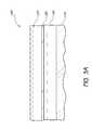
- FIG. 6is a schematic, cross-sectional side view of the partially formed integrated circuit of FIGS. 5A and 5B after depositing a layer of a spacer material, in accordance with embodiments of the invention.
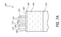
- FIGS. 7A and 7Bare schematic, cross-sectional side and top plan views of the partially formed integrated circuit of FIG. 6 after a spacer etch, in accordance with embodiments of the invention.
- FIGS. 8A and 8Bare schematic, cross-sectional side and top plan views of the partially formed integrated circuit of FIGS. 7A and 7B after removing a remaining portion of the temporary layer to leave a pattern of spacers in the array region of the integrated circuit, in accordance with embodiments of the invention.
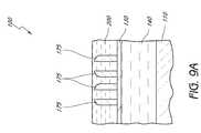
- FIGS. 9A and 9Bare schematic, cross-sectional side and top plan views of the partially formed integrated circuit of FIGS. 8A and 8B after depositing photoresist between and over the spacers, in accordance with embodiments of the invention.
- FIGS. 10A and 10Bare schematic, cross-sectional side and top plan views of the partially formed integrated circuit of FIGS. 9A and 9B after forming a pattern in the photoresist, in accordance with embodiments of the invention.
- FIG. 11is a schematic, cross-sectional side view of the partially formed integrated circuit of FIGS. 10A and 10B after transferring a combined pattern defined by the patterned photoresist and the spacers to an underlying hard mask layer, in accordance with embodiments of the invention.
- FIG. 12is a schematic, cross-sectional side view of the partially formed integrated circuit of FIG. 11 after transferring the combined pattern to a primary mask layer, in accordance with embodiments of the invention.
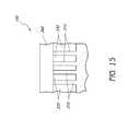
- FIG. 13is a schematic, cross-sectional side view of the partially formed integrated circuit of FIG. 12 after transferring the combined pattern to the underlying substrate, in accordance with embodiments of the invention.
- FIGS. 14A and 14Bare schematic, cross-sectional side and top views of the partially formed integrated circuit of FIG. 13 after transferring the pattern into the substrate and removing hard mask layers overlying the substrate, in accordance with embodiments of the invention.
- FIG. 15is a schematic, cross-sectional side view of the partially formed integrated circuit of FIGS. 14A and 14B after filling trenches with a dielectric and forming a sequence of layers corresponding to a gate stack, in accordance with embodiments of the invention.
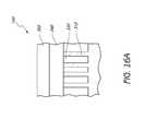
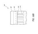
- FIGS. 16A , 16 B and 16 Care schematic, cross-sectional side and top plan views of the partially formed integrated circuit of FIG. 15 after depositing and patterning a photoresist layer, in accordance with embodiments of the invention.
- FIGS. 17A and 17Bare schematic, cross-sectional side and top plan views of the partially formed integrated circuit of FIGS. 16A and 16B after transferring the pattern from the photoresist layer to the sequence of gate stack layers, in accordance with embodiments of the invention.
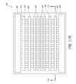
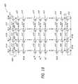
- FIG. 18is a schematic diagram of a memory cell array of a NAND flash memory device, in accordance with embodiments of the invention.
- FIG. 19is a system block diagram illustrating an electronic device including a memory device, in accordance with embodiments of the invention.
- Pitch multiplicationhas the ability to form closely spaced lines by patterning those lines using a mask formed by spacers. Because the spacers are formed on sidewalls of mandrels, the spacers typically form a continuous loop. Using these continuous loops to pattern a substrate may form continuous loops of material in the substrate. However, separated lines are typically desired for use in various applications, such as bit lines or word lines in a memory device. Thus, to utilize the closely spaced pairs of lines patterned using a spacer loop, the ends of the loops are typically etched to physically, electrically disconnect different legs of the loops from each other. Methods and structures for such an etch (called a loop etch) are described in U.S. Pat. No. 7,151,040, the entire disclosure of which is incorporated by reference herein.
- loop end etchingmay involve deposition, patterning and material removal steps. It will be appreciated that the patterning step may involve performing photolithography and exposure of protective material to light through a mask. Due to the time needed to perform these steps and, possibly, the time needed to transport a substrate between processing equipment to perform these steps, the loop etch can undesirably add to the time and complexity involved in, e.g., fabricating an integrated circuit using pitch multiplication.
- different legs of a semiconductor loopare electrically isolated without needing to perform a loop etch. Rather, isolation transistors are formed in the loops to electrically isolate the different legs from each other.
- a gateis formed over the loop of semiconductor material and the regions of the loop neighboring the gate are doped to form source and drain regions.
- the loop region directly below the gatefunctions as an active area.
- the gateis biased in the off state to prevent current flow through the active area, thereby electrically isolating from each other the parts of the loop that lie on either side of the gate.
- an isolation transistoris formed at the ends of each leg of the loops, for a total of four such transistors per loop.
- the isolation transistorsdefine two electrically isolated legs of semiconductor material between each pair of transistors.
- the loops of semiconductor materialare formed by a pitch multiplication process.
- Spacer loopsare formed on a level over a substrate.
- a block of masking materialis overlaid on a section of each of the loops, e.g., a different block of masking material is overlaid on each end of the loops in embodiments where the loops are substantially parallel lines of material joined together at their ends.
- the pattern defined by the spacer loops and the blocks of masking materialare transferred to a substrate, thereby forming lines of semiconductor material that terminate at and are contiguous with the blocks of the semiconductor material.
- a transistor gateis formed on each line of semiconductor material and adjacent each block of semiconductor material.
- the block of semiconductor material and the part of the line on a side of the gate opposite the blockare doped to form source/drain regions.
- the blocks and the gateare electrically tied together and are biased in the off state to electrically isolate the lines of semiconductor material from the blocks.
- each line disposed between the blocksis electrically isolated from other lines without needing to perform a loop etch.
- the steps for forming the isolation transistorsare typically already part of a process flow for forming other transistors, e.g., the isolation transistors can be formed using the same patterning, doping and deposition steps used to form floating gate transistors and select gates in a memory device.
- the formation of the isolation transistorsdo not introduce any additional steps to the process flow.
- the process steps involved in the loop etchcan be omitted.
- the process flowis simplified and process throughput is increased.
- linesmay be formed having a pitch below the minimum pitch of the photolithographic method used to pattern the various photoresist layers illustrated herein.
- embodiments of the inventionallow the formation of lines having a pitch of about 100 nm or less or about 50 nm or less.
- mask featuresare formed by pitch multiplication.
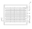
- FIG. 2shows a top view of a portion of a partially fabricated integrated circuit 100 .
- the embodiments of the inventionmay be used to form any integrated circuit and may be applied to form masks for patterning various substrates, they may particularly advantageously be applied to form devices having arrays of electrical devices, including memory cell arrays for volatile and non-volatile memory devices such as DRAM, ROM or flash memory, including NAND or NOR flash memory, or integrated circuits having logic or gate arrays.
- the logic arraymay be a field programmable gate array (FPGA) having a core array similar to a memory array and a periphery with supporting logics.
- the integrated circuit 100may be, e.g., a memory chip or a processor, which may include both a logic array and embedded memory, or any other integrated circuit having a logic or a gate array.
- a central region 102is surrounded by a peripheral region 104 , the “periphery.”
- the array 102will typically be densely populated with electrically conductive line and electrical devices, including transistors and/or capacitors.
- the electrical devicesform a plurality of memory cells, which may be arranged in a regular grid pattern at the intersection of word lines and bit lines.
- pitch multiplicationmay be used to form features such as rows/columns of transistors and/or capacitors in the array 102 , as discussed herein.
- the periphery 104typically comprises features larger than those in the array 102 .
- Conventional photolithographyis preferably used to pattern features, such as logic circuitry, in the periphery 104 , because the geometric complexity of logic circuits located in the periphery 104 makes using pitch multiplication difficult, whereas the regular grid typical of array patterns is conducive to pitch multiplication.
- some devices in the peripheryrequire larger geometries due to electrical constraints, thereby making pitch multiplication less advantageous than conventional photolithography for such devices.
- the periphery 104may contain patterns/circuits defined by both conventional lithography and pitch multiplication.
- the relative positions, and the number of periphery 104 and array 102 regions in the partially fabricated integrated circuit 100may vary from that depicted.
- FIG. 3Ashows a cross-sectional side view of the partially formed integrated circuit 100 .
- Various masking layers 120 - 140are provided above a substrate 110 .
- the layers 120 - 140will be etched to form a mask for patterning the substrate 110 , as discussed below.
- a selectively definable layer 120overlies a hard mask, or etch stop, layer 130 , which overlies a primary mask layer 140 , which overlies the substrate 110 to be processed (e.g., etched) through a mask.
- the materials for the layers 120 - 140 overlying the substrate 110are chosen based upon consideration of the chemistry and process conditions for the various pattern forming and pattern transferring steps discussed herein. Because the layers between the topmost selectively definable layer 120 and the substrate 110 function to transfer a pattern derived from the selectively definable layer 120 to the substrate 110 , the layers 130 - 140 between the selectively definable layer 120 and the substrate 110 are chosen so that they may be selectively etched relative to other exposed materials. It will be appreciated that a material is considered selectively, or preferentially, etched when the etch rate for that material is at least about 2-3 times greater, at least about 10 times greater, at least about 20 times greater, or at least about 40 times greater than that for surrounding materials.
- a goal of the layers 120 - 130 overlying the primary hard mask layer 140is to allow well-defined patterns to be formed in that layer 140 , it will be appreciated that one or more of the layers 120 - 130 may be omitted or substituted if suitable other materials, chemistries and/or process conditions are used.
- the primary hard mask layer 140may be omitted and patterns may be transferred directly to the substrate using the hard mask layer 130 .
- the selectively definable layer 120is photodefinable, e.g., formed of a photoresist, including any photoresist, including any positive or negative photoresist, known in the art.
- the photoresistmay be any photoresist compatible with 157 nm, 193 nm, 248 nm or 365 nm wavelength systems, 193 nm wavelength immersion systems, extreme ultraviolet systems (including 13.7 nm wavelength systems) or electron beam lithographic systems.
- maskless lithography, or maskless photolithographymay be used to define the selectively definable layer 120 .
- photoresist materialsinclude argon fluoride (ArF) sensitive photoresist, i.e., photoresist suitable for use with an ArF light source, and krypton fluoride (KrF) sensitive photoresist, i.e., photoresist suitable for use with a KrF light source.
- ArF photoresistsare used with photolithography systems utilizing relatively short wavelength light, e.g., 193 nm wavelength light.
- KrF photoresistsare used with longer wavelength photolithography systems, such as 248 nm systems.
- the layer 120 and any subsequent resist layersmay be formed of a resist that may be patterned by nano-imprint lithography, e.g., by using a mold or mechanical force to pattern the resist.
- the material for the hard mask layer 130comprises an inorganic material.
- Materials for the hard mask layer 130include silicon oxide (SiO 2 ), silicon or an anti-reflective coating (ARC), such as a silicon-rich silicon oxynitride, a silicon-rich nitride, or a film that has the desired etch selectivity relative to the spacers 175 or other exposed materials ( FIG. 7A ).
- the hard mask layer 130may also include combinations of layers of materials, e.g., a bottom anti-reflective coating (BARC) over a dielectric anti-reflective coating (DARC).
- BARCbottom anti-reflective coating
- DARCdielectric anti-reflective coating
- the hard mask layer 130is an anti-reflective coating, such as DARC.
- ARCsfor the hard mask layer 130 may be particularly advantageous for forming patterns having pitches near the resolution limits of a photolithographic technique.
- the ARCscan enhance resolution by minimizing light reflections, thus increasing the precision with which photolithography can define the edges of a pattern.
- embodiments of the inventionmay utilize a primary masking layer to facilitate pattern transfer to a substrate.
- a primary masking layermay be formed of amorphous carbon.
- the amorphous carbon layermay be formed by chemical vapor deposition using a hydrocarbon compound, or mixtures of such compounds, as carbon precursors.
- Carbon precursorsmay include propylene, propyne, propane, butane, butylene, butadiene and acetelyne.
- a method for forming amorphous carbon layersis described in U.S. Pat. No. 6,573,030 B1, issued to Fairbairn et al. on Jun. 3, 2003, the entire disclosure of which is incorporated herein by reference.
- the amorphous carbonis a form of amorphous carbon that is highly transparent to light and that offers further improvements for photo alignment by being transparent to the wavelengths of light used for such alignment.
- amorphous carbonmay be doped.
- a suitable method for forming doped amorphous carbonis described in U.S. patent application Ser. No. 10/652,174 to Yin et al., the entire disclosure of which is incorporated herein by reference.
- the “substrate” to which patterns are transferredmay include a layer of a single material, a plurality of layers of different materials, a layer or layers having regions of different materials or structures in them, etc. These materials may include semiconductors, insulators, conductors, or combinations thereof.
- the substrateis formed of doped semiconductor material, e.g., semiconductor material containing p-type dopant.
- the trenches 122may be formed by, e.g., photolithography with 248 nm or 193 nm light, in which the layer 120 is exposed to radiation through a reticle and then developed. After being developed, the remaining photodefinable material, photoresist in the illustrated embodiment, forms mask features such as the illustrated lines 124 (shown in cross-section only).
- the pitch of the resulting lines 124is equal to the sum of the width of a line 124 and the width of a neighboring space 122 .
- the pitchmay be at or near the limits of the photolithographic technique used to pattern the photodefinable layer 120 .
- the pitch of the lines 124may be about 100 nm.
- the pitchmay be at the minimum pitch of the photolithographic technique and the spacer pattern discussed below may advantageously have a pitch below the minimum pitch of the photolithographic technique.
- the lines 124may be formed having larger feature sizes, e.g., 200 nm or more, to minimize errors in the position and sizes of the lines 124 .
- the spaces 122are widened by etching the photoresist lines 124 , to form modified spaces 122 a and lines 124 a .
- the photoresist lines 124are etched using an isotropic etch to “shrink” or trim those features. Suitable etches include etches using an oxygen-containing plasma, e.g., a SO 2 /O 2 /N 2 /Ar plasma, a Cl 2 /O 2 /He plasma or a HBr/O 2 /N 2 plasma.
- the extent of the etchis selected so that the widths of the lines 124 a are substantially equal to the desired spacing between the later-formed spacers 175 ( FIG.
- the width of the lines 124may be reduced from about 80-120 nm to about 30-70 nm or about 50-70 nm.
- the width-reducing etchallows the lines 124 a to be narrower than would otherwise be possible using the photolithographic technique used to pattern the photodefinable layer 120 . While the critical dimensions of the lines 124 a may be etched below the resolution limits of the photolithographic technique, it will be appreciated that this etch does not alter the pitch of the spaces 122 a and lines 124 a , since the distance between identical points in these features remains the same.
- a layer 170 of spacer materialis blanket deposited conformally over exposed surfaces, including the hard mask layer 150 and the top and sidewalls of the temporary layer 140 .
- the spacer materialmay be any material that can act as a mask for transferring a pattern to the underlying hard mask layer 130 .
- the spacer materialmay be, without limitation, silicon, silicon oxide and silicon nitride. In the illustrated embodiment, the spacer material is silicon oxide, which provides particular advantages in combination with other selected materials of the masking stack.
- Methods for spacer material depositioninclude atomic layer deposition, e.g., using a self-limiting deposition with a silicon precursor and a subsequent exposure to an oxygen or nitrogen precursor to form silicon oxides and nitrides, respectively.
- a silicon halidesuch as silicon hexachlorodisilane (HCD)
- H 2 Ooxygen precursor
- ALDcan be performed at relatively low temperatures, e.g., under about 200° C. or under about 100° C., which has advantages for preventing thermal damage to underlying carbon-based materials, such as photoresist and amorphous carbon layers.
- chemical vapor depositionis used to deposit the spacer material, e.g., using O 3 and TEOS to form silicon oxide.
- the thickness of the layer 170is determined based upon the desired width of the spacers 175 ( FIG. 7A ). For example, in some embodiments, the layer 170 is deposited to a thickness of about 20-80 nm or about 40-60 nm to form spacers of roughly similar widths. The step coverage is about 80% or greater and or about 90% or greater.
- the silicon oxide spacer layer 170is subjected to an anisotropic etch to remove spacer material from horizontal surfaces 180 of the partially formed integrated circuit 100 .
- the selectively definable layer 120is next removed to leave freestanding spacers 175 .
- the selectively definable layer 120may be selectively removed using an organic strip process.
- the spacers 175form elongated loops and have substantially parallel legs which are joined at their ends.
- the pitch of the spacers 175is roughly half that of the photoresist lines 124 and spaces 122 ( FIGS. 4A and 4B ) originally formed by photolithography. Where the photoresist lines 124 had a pitch of about 200 nm, spacers 175 having a pitch of about 100 nm or less may be formed.
- the spacers 175are formed on the sidewalls of the features or lines 124 b , the spacers 175 generally follow the outline of the pattern of features or lines 124 a in the modified photodefinable layer 120 a and, so, form a closed loop in the spaces 122 a between the lines 124 a.
- blocks of mask materialare overlaid the spacers 175 and the resulting pattern is transferred to the substrate 110 .
- a layer 200 of mask materiale.g., photoresist
- the photoresist layer 200can be formed of positive or negative photoresist.
- the photodefinable layer 200is patterned by photolithography to form masking material blocks 210 , 212 at the ends of the loops of spacers 175 .
- the blocks 210 , 212extend across and contact opposite ends of the spacers 175 .
- the blocks 210 , 212have dimensions sufficiently large to be patterned with photolithography and without performing pitch multiplication.
- a mixed pattern 177 formed of pitch multiplied and non-pitch multiplied mask featurescan be formed.
- the blocks 210 , 212may be patterned simultaneously with other relatively large features formed in the periphery region of the partially fabricated integrated circuit 100 .
- the pattern 177 defined by the blocks 210 , 212 and the spacers 175is transferred to the hard mask layer 130 .
- the pattern transfermay be accomplished by, e.g., anisotropically etching the hard mask layer 130 .
- the pattern 177is transferred to the primary mask layer 140 .
- the pattern transfermay be accomplished by, e.g., anisotropically etching the primary mask layer 140 .
- the pattern 177is transferred to the substrate 110 using an anisotropic etch with the layer 140 acting as a mask for the etch.
- the spacers 175 and mask layers 130 and 140 overlying the substrate 110are removed.
- Pitch multiplied lines 310are formed in the substrate 110 . At each of their ends, the lines 310 contact laterally separated blocks 320 , 322 .
- trenches defined by the lines 310 and blocks 320 , 322are filled with insulating material 330 , e.g., silicon oxide, for shall trench isolation applications.
- insulating material 330e.g., silicon oxide
- Memory cell active areassuch as for flash memory, may be defined between the trenches and floating and control gates may be formed over the active areas.
- a stack of layers 340 for forming the floating and control gatesis subsequently formed over the lines 310 , insulating material 330 and blocks 320 , 322 ( FIG. 14B ).
- the composition of the layers 340can vary across the partially fabricated integrated circuit 100 .
- the layers 340can include layers appropriate for the formation of these gates.
- the layers 340can include fewer layers, as appropriate for formation of the select gate.
- the layers 340may include a silicide layer over a polysilicon layer, which overlies an oxide-nitride-oxide (ONO) composite layer, which overlies a polysilicon layer.
- ONOoxide-nitride-oxide
- a mask layer 350is formed over the stack of layers 340 .
- the mask layer 350may be a selectively definable layer 350 formed of, e.g., photoresist.
- the layer 350is subsequently patterned, thereby forming elongated strips 352 - 356 .
- the patterned elongated strips 352 - 356may be used to form various features in a memory device.
- the strips 352 - 355may be used to form select gates for regulating reading and writing to memory cells formed along the lines 310 , which form active areas.
- the strips 356may be used to define word lines and floating and control gates.
- the strips 352 - 356may be formed in a single step, e.g., by photolithography, or in multiple separate steps. For example, to increase density, the strips 356 may be formed by pitch multiplication. As such, a stack of masking layers as described herein with reference to FIGS. 3A and 3B can be formed over the layers 340 . The stack of masking layers may then be processing as discussed herein with reference to FIGS. 3A-8B . The resulting spacer loops may then be subjected to a loop etch, thereby forming the strips 356 . The mask layer 350 ( FIG. 16A ) may subsequently be deposited between and over the spacers 175 .
- the mask layer 350is then patterned, e.g., by photolithography where the mask layer 350 is formed of photoresist, thereby forming the strips 352 - 355 ( FIGS. 16B and 16C ). While not illustrated for ease of discussion, as discussed herein, one or more additional masking layers may be provided between the mask layer 350 to facilitate pattern transfer to the layers 340 . For example, an ARC layer may be provided directly beneath the mask layer 350 and an amorphous carbon layer may be provided between the ARC layer and the layer 340 . Such a sequence of layers would provide the advantages and could be utilized as noted above for the layers 130 and 140 ( FIGS. 3A-13 ).
- the pattern in the mask layer 350is then transferred to the layers 340 , thereby forming strips 342 - 346 in those layers.
- the strips 342 - 346may correspond to word lines, floating gates, control gates and select gates in those layers.
- the exposed parts of the lines 310 and blocks 320 , 322 of semiconductor materialare doped (e.g., with an n-type dopant) to form source/drain regions in the lines 310 and blocks 320 , 322 on either side of the strips 342 - 346 .
- the feature 320forms a source and the feature 342 form a gate of isolation transistors for each of the lines 310 .
- the feature 322forms a source and the feature 343 form a gate of additional isolation transistors for each of the lines 310 .
- contactsare made to the various bit and word lines and the bit and word lines are connected to various ancillary circuitry to form a memory device.
- the contactsmay be made from a level above the bit and word lines.
- contacts to the source regions 320 , 322can be electrically connected to the gates 342 , 343 , respectively, so that the gates and sources of the isolation transistors are tied together for simplicity of operation and reliability, as discussed herein.
- FIG. 18illustrates a block of a NAND flash memory array in a memory device 400 according to some embodiments of the invention.
- the illustrated flash memory arrayincludes bit lines BL 0 to BLM and word lines WL 0 to WLN.
- the bit lines BL 0 -BLMextend parallel to one another in a column direction.
- the word lines WL 0 -WLNextend parallel to one another in a row direction.
- the NAND flash memory arrayalso includes select transistors 402 , 404 used for selecting a bit line.
- Ancillary logic and other circuitry(not shown) connect to the bit lines using the bit line contacts 406 .
- the gates of the rows of select transistors 402 , 404correspond to the features 344 , 345 ( FIG. 17B ).
- Each bit lineincludes a string of floating gate transistors coupled in series, source to drain.
- the second bit line BL 1includes floating gate transistors 110 connected in series.
- the control gates of floating gate transistors 110 of cells in the same roware coupled to the same word line.
- Each of the floating gate transistors 110forms a memory cell that stores a charge (or a lack of charge), wherein the amount of stored charge can be used to represent, for example, one or more states, and wherein the one or more states can represent one or more digits (e.g., bits) of data.
- the bitis read by detecting the absence or presence of charge.
- bit lines BL 0 to BLMare shunted together at their ends.
- Isolation, or select, transistors 412 , 414electrically isolate individual bit lines from each other by preventing current flow to the shunted ends of the bit lines.
- the shunted endscorrespond to the blocks 320 and 322 ( FIG. 17B ) and the gates of the select transistors 412 , 414 correspond to the features 342 , 343 ( FIG. 17B ).
- each pair of bit lineswhich can also be viewed as a loop of semiconductor material, may include a total of four isolation transistors.
- isolation transistors 412 a and 412 bconstitute first and second isolation transistors proximate one end of the loop and isolation transistors 414 a and 414 b constitute third and fourth isolation transistors proximate an opposite end of the loop.
- a pair of isolation transistorsmay be utilized to electrically isolate a single bit line, which are formed by substantially parallel, horizontally elongated portions of the loops. The isolation transistors isolate the expanse of one of these elongated portions from an expanse of another of these elongated portions.
- the source/drain regions of the select transistors 412 , 414are electrically tied or connected to the gates of these transistors and are biased in an off state.
- the gates and tied source/drainscan be left floating or connected to ground (0V), thereby electrically isolating all bit lines connected to the isolation transistors 412 , 414 .
- the transistors 412 , 414may be in an “on” state. However, because all memory cells are erased simultaneously, the state of the transistors 412 , 414 is irrelevant; there is no need to isolate individual bit lines, since the same operation is performed on all cells of the NAND flash memory block.
- a fully formed integrated circuit 101 formed from the partially fabricated integrated circuit 100can be incorporated into various systems or devices.
- the integrated circuit 101can be utilized as memory for storing data in an electronic device 102 having a computer processor 103 , a user interface 104 and power source 105 .
- Examples of such electronic devicesinclude computerized devices, including any device utilizing a memory circuit, such as data storage and retrieval devices, including music, photo and/or video devices.
- the blocksare advantageously for simplifying operation of the isolation transistors and for improving process results. By tying all the loops together, individual access to the loops is obviated, thereby simplifying fabrication and operation of the isolation transistors. Moreover, the blocks can improve process results by facilitating deposition of dielectric into the trenches 312 ( FIG. 14B ). It has been found that the ends of pitch multiplied loops can be relatively thin relative to mid-portions of the loops. It has also been found that deposition of dielectric into these relatively thin ends can be difficult and prone to void formation. By eliminating these ends by overlying the ends with blocks of masking material, it has been found that filling of the trenches can be improved, leading to integrated circuits with improved reliability.
- the isolation transistorscan be omitted from one end of the loops of material.
- the materialis shunted together for another reason, e.g., where the lines forming the loop are all tied to ground at one end, it may be unnecessary to form an isolation transistor to electrically isolate the lines on the end that is tied to ground.
- the formation of block of material at the ends of the loopshas benefits for improving filling of trenches defined by the lines. As a result, it may be desirable to form the blocks at both loop ends, even where electrical isolation is not necessary at one end.
- linesof material need not extend in only a single direction through the entire extent of the “lines”. Rather, a “line” of material is an elongated run of material and may curve or otherwise change direction over the expanse of the line of material.
- transferring a pattern from an overlying level to an underlying levelinvolves forming features in the underlying level that generally correspond to features in the overlying level.
- the path of lines in the underlying levelwill generally follow the path of lines in the overlying level and the location of other features in the underlying level will correspond to the location of similar features in the overlying level.
- the precise shapes, and sizes of featuresmay vary from the overlying level to the underlying level, however.
- the sizes of and relative spacings between the features forming the transferred patternmay be enlarged or diminished relative to the pattern on the overlying level, while still resembling the same initial “pattern,” as can be seen from the example of shrinking the first resist mask in the embodiments described below.
- the transferred patternis still considered to be the same pattern as the initial pattern.
- forming spacers around mask featuresmay change the pattern.
- a methodcomprises providing a substrate having a loop formed of semiconductor material.
- the loopis defined by a pair of substantially parallel, horizontally elongated portions joined at at least one loop end.
- a first transistor along the loopis formed to electrically isolate an expanse of a first of the elongate portions from an expanse of a second of the elongate portions.
- a part of the loopforms an active area of the first transistor.
- a processfor forming an integrated circuit.
- the processcomprises providing a plurality of mandrels overlying a substrate.
- a spacersare provided at sidewalls of the mandrels.
- the mandrelsare selectively removed relative to the spacers.
- a layer of mask materialis deposited over the spacers.
- the layer of mask materialis patterned to form first and second laterally-separated blocks of the mask material, the first block contacting a first end of each of the spacers and the second block contacting a second end of each of the spacers.
- a first pattern defined by the spacers and the first and second blocksare transferred to the substrate.
- a process for forming an integrated circuitcomprises providing a plurality of elongated loops of a first mask material overlying a substrate.
- a layer of a second mask materialis provided over the loops.
- the layeris patterned to form a block of the second mask material, the block contacting an end of each of the loops.
- a first pattern defined by the loops and the blockis transferred to the substrate.
- a layer of semiconductor materialis subsequently formed over the substrate.
- An other layer of mask materialis formed over the semiconductor material.
- the other layeris patterned to form one or more strips of masking material extending across and contacting each of the loops.
- a second pattern defined by the stripsis transferred to the layer of semiconductor material to form strips of semiconductor material.
- the strips of semiconductor materialare electrically connected to substrate features defined by the block of the second mask material.
- an integrated circuitcomprises a plurality of spaced apart lines of semiconductor material.
- a first block of the semiconductor materialis disposed on a same level as the lines of semiconductor material and contact a first end of each of the elongate strips.
- a first plurality of transistor gatesis disposed along the lines of semiconductor material. The first plurality of transistor gates are electrically connected to the first block.
- an electrical devicecomprising an integrated circuit.
- the integrated circuitcomprises a plurality of spaced-apart lines of semiconductor material. All of a first end of the lines are electrically interconnected and all of an opposite end of the lines are electrically interconnected. A means for preventing current flow from a mid-portion of the lines to the first end is provided.
Landscapes
- Engineering & Computer Science (AREA)
- Physics & Mathematics (AREA)
- Microelectronics & Electronic Packaging (AREA)
- General Physics & Mathematics (AREA)
- Computer Hardware Design (AREA)
- Condensed Matter Physics & Semiconductors (AREA)
- Power Engineering (AREA)
- Manufacturing & Machinery (AREA)
- Chemical & Material Sciences (AREA)
- Inorganic Chemistry (AREA)
- Geometry (AREA)
- Semiconductor Memories (AREA)
- Non-Volatile Memory (AREA)
- Element Separation (AREA)
- Insulated Gate Type Field-Effect Transistor (AREA)
Abstract
Description
Claims (23)
Priority Applications (4)
| Application Number | Priority Date | Filing Date | Title |
|---|---|---|---|
| US13/777,803US8932960B2 (en) | 2007-12-18 | 2013-02-26 | Methods for isolating portions of a loop of pitch-multiplied material and related structures |
| US14/592,498US9666695B2 (en) | 2007-12-18 | 2015-01-08 | Methods for isolating portions of a loop of pitch-multiplied material and related structures |
| US15/596,288US9941155B2 (en) | 2007-12-18 | 2017-05-16 | Methods for isolating portions of a loop of pitch-multiplied material and related structures |
| US15/925,418US10497611B2 (en) | 2007-12-18 | 2018-03-19 | Methods for isolating portions of a loop of pitch-multiplied material and related structures |
Applications Claiming Priority (3)
| Application Number | Priority Date | Filing Date | Title |
|---|---|---|---|
| US11/959,409US7790531B2 (en) | 2007-12-18 | 2007-12-18 | Methods for isolating portions of a loop of pitch-multiplied material and related structures |
| US12/845,167US8390034B2 (en) | 2007-12-18 | 2010-07-28 | Methods for isolating portions of a loop of pitch-multiplied material and related structures |
| US13/777,803US8932960B2 (en) | 2007-12-18 | 2013-02-26 | Methods for isolating portions of a loop of pitch-multiplied material and related structures |
Related Parent Applications (1)
| Application Number | Title | Priority Date | Filing Date |
|---|---|---|---|
| US12/845,167DivisionUS8390034B2 (en) | 2007-12-18 | 2010-07-28 | Methods for isolating portions of a loop of pitch-multiplied material and related structures |
Related Child Applications (1)
| Application Number | Title | Priority Date | Filing Date |
|---|---|---|---|
| US14/592,498ContinuationUS9666695B2 (en) | 2007-12-18 | 2015-01-08 | Methods for isolating portions of a loop of pitch-multiplied material and related structures |
Publications (2)
| Publication Number | Publication Date |
|---|---|
| US20130171784A1 US20130171784A1 (en) | 2013-07-04 |
| US8932960B2true US8932960B2 (en) | 2015-01-13 |
Family
ID=40752074
Family Applications (6)
| Application Number | Title | Priority Date | Filing Date |
|---|---|---|---|
| US11/959,409Active2028-07-02US7790531B2 (en) | 2007-12-18 | 2007-12-18 | Methods for isolating portions of a loop of pitch-multiplied material and related structures |
| US12/845,167Active2028-06-04US8390034B2 (en) | 2007-12-18 | 2010-07-28 | Methods for isolating portions of a loop of pitch-multiplied material and related structures |
| US13/777,803ActiveUS8932960B2 (en) | 2007-12-18 | 2013-02-26 | Methods for isolating portions of a loop of pitch-multiplied material and related structures |
| US14/592,498ActiveUS9666695B2 (en) | 2007-12-18 | 2015-01-08 | Methods for isolating portions of a loop of pitch-multiplied material and related structures |
| US15/596,288ActiveUS9941155B2 (en) | 2007-12-18 | 2017-05-16 | Methods for isolating portions of a loop of pitch-multiplied material and related structures |
| US15/925,418Active2028-02-08US10497611B2 (en) | 2007-12-18 | 2018-03-19 | Methods for isolating portions of a loop of pitch-multiplied material and related structures |
Family Applications Before (2)
| Application Number | Title | Priority Date | Filing Date |
|---|---|---|---|
| US11/959,409Active2028-07-02US7790531B2 (en) | 2007-12-18 | 2007-12-18 | Methods for isolating portions of a loop of pitch-multiplied material and related structures |
| US12/845,167Active2028-06-04US8390034B2 (en) | 2007-12-18 | 2010-07-28 | Methods for isolating portions of a loop of pitch-multiplied material and related structures |
Family Applications After (3)
| Application Number | Title | Priority Date | Filing Date |
|---|---|---|---|
| US14/592,498ActiveUS9666695B2 (en) | 2007-12-18 | 2015-01-08 | Methods for isolating portions of a loop of pitch-multiplied material and related structures |
| US15/596,288ActiveUS9941155B2 (en) | 2007-12-18 | 2017-05-16 | Methods for isolating portions of a loop of pitch-multiplied material and related structures |
| US15/925,418Active2028-02-08US10497611B2 (en) | 2007-12-18 | 2018-03-19 | Methods for isolating portions of a loop of pitch-multiplied material and related structures |
Country Status (7)
| Country | Link |
|---|---|
| US (6) | US7790531B2 (en) |
| EP (1) | EP2232539B1 (en) |
| JP (3) | JP5561485B2 (en) |
| KR (1) | KR101603800B1 (en) |
| CN (2) | CN103904085B (en) |
| TW (1) | TWI503924B (en) |
| WO (1) | WO2009079517A2 (en) |
Cited By (3)
| Publication number | Priority date | Publication date | Assignee | Title |
|---|---|---|---|---|
| US20150123185A1 (en)* | 2007-12-18 | 2015-05-07 | Micron Technology, Inc. | Methods for isolating portions of a loop of pitch-multiplied material and related structures |
| US20150170905A1 (en)* | 2007-07-30 | 2015-06-18 | Micron Technology, Inc. | Methods for device fabrication using pitch reduction and related devices |
| US10515801B2 (en) | 2007-06-04 | 2019-12-24 | Micron Technology, Inc. | Pitch multiplication using self-assembling materials |
Families Citing this family (34)
| Publication number | Priority date | Publication date | Assignee | Title |
|---|---|---|---|---|
| US8481417B2 (en) | 2007-08-03 | 2013-07-09 | Micron Technology, Inc. | Semiconductor structures including tight pitch contacts and methods to form same |
| US8030218B2 (en) | 2008-03-21 | 2011-10-04 | Micron Technology, Inc. | Method for selectively modifying spacing between pitch multiplied structures |
| JP2009295785A (en)* | 2008-06-05 | 2009-12-17 | Toshiba Corp | Method of manufacturing semiconductor device |
| US8076208B2 (en) | 2008-07-03 | 2011-12-13 | Micron Technology, Inc. | Method for forming transistor with high breakdown voltage using pitch multiplication technique |
| JP5665289B2 (en) | 2008-10-29 | 2015-02-04 | 株式会社日立国際電気 | Semiconductor device manufacturing method, substrate processing method, and substrate processing apparatus |
| KR101045090B1 (en)* | 2008-11-13 | 2011-06-29 | 주식회사 하이닉스반도체 | Method of forming fine pattern of semiconductor device |
| US8492282B2 (en) | 2008-11-24 | 2013-07-23 | Micron Technology, Inc. | Methods of forming a masking pattern for integrated circuits |
| KR101077453B1 (en)* | 2009-03-31 | 2011-10-26 | 주식회사 하이닉스반도체 | Method for Forming Pattern of Semiconductor device |
| JP4982582B2 (en)* | 2010-03-31 | 2012-07-25 | 株式会社東芝 | Mask manufacturing method |
| KR101150639B1 (en)* | 2010-06-17 | 2012-07-03 | 에스케이하이닉스 주식회사 | Method for forming pattern of the semiconductor device |
| US8764999B2 (en)* | 2010-11-23 | 2014-07-01 | Tokyo Electron Limited | Sidewall image transfer pitch doubling and inline critical dimension slimming |
| KR20120062385A (en)* | 2010-12-06 | 2012-06-14 | 에스케이하이닉스 주식회사 | Method of manufacturing semiconductor memory device |
| US8536674B2 (en) | 2010-12-20 | 2013-09-17 | General Electric Company | Integrated circuit and method of fabricating same |
| US9525007B2 (en)* | 2010-12-28 | 2016-12-20 | Micron Technology, Inc. | Phase change memory device with voltage control elements |
| TWI473205B (en)* | 2011-11-24 | 2015-02-11 | Powerchip Technology Corp | Method for forming contact hole |
| US8802510B2 (en)* | 2012-02-22 | 2014-08-12 | Taiwan Semiconductor Manufacturing Company, Ltd. | Methods for controlling line dimensions in spacer alignment double patterning semiconductor processing |
| US8889561B2 (en) | 2012-12-10 | 2014-11-18 | Globalfoundries Inc. | Double sidewall image transfer process |
| KR102059183B1 (en) | 2013-03-07 | 2019-12-24 | 삼성전자주식회사 | Method of forming semiconductor device and the device |
| JP6091940B2 (en)* | 2013-03-11 | 2017-03-08 | 株式会社日立国際電気 | Semiconductor device manufacturing method, substrate processing apparatus, and program |
| US9177797B2 (en)* | 2013-12-04 | 2015-11-03 | Taiwan Semiconductor Manufacturing Company, Ltd. | Lithography using high selectivity spacers for pitch reduction |
| US9029263B1 (en)* | 2013-12-12 | 2015-05-12 | Texas Instruments Incorporated | Method of printing multiple structure widths using spacer double patterning |
| US9324619B2 (en)* | 2014-08-25 | 2016-04-26 | Samsung Electronics Co., Ltd. | Semiconductor device and method of fabricating the same |
| KR102290460B1 (en)* | 2014-08-25 | 2021-08-19 | 삼성전자주식회사 | Semiconductor device and method of manufacturing the same |
| JP6382055B2 (en)* | 2014-10-07 | 2018-08-29 | 東京エレクトロン株式会社 | Method for processing an object |
| US9673055B2 (en) | 2015-02-04 | 2017-06-06 | Globalfoundries Inc. | Method for quadruple frequency FinFETs with single-fin removal |
| US9882028B2 (en)* | 2016-06-29 | 2018-01-30 | International Business Machines Corporation | Pitch split patterning for semiconductor devices |
| JP6814377B2 (en)* | 2016-10-20 | 2021-01-20 | 東京エレクトロン株式会社 | How to reduce overlay errors in via-to-grid patterning |
| EP3419047A1 (en) | 2017-06-22 | 2018-12-26 | IMEC vzw | A method for patterning a target layer |
| CN110581066B (en)* | 2018-06-07 | 2024-06-21 | 长鑫存储技术有限公司 | Manufacturing method of multiple mask layer |
| CN110767538B (en)* | 2018-07-26 | 2024-06-07 | 长鑫存储技术有限公司 | Layout structure and method for forming semiconductor integrated circuit device |
| EP3723112B1 (en)* | 2019-04-09 | 2023-12-20 | Imec Vzw | Method for forming a gate mask layer |
| US11011581B2 (en)* | 2019-06-10 | 2021-05-18 | Western Digital Technologies, Inc. | Multi-level loop cut process for a three-dimensional memory device using pitch-doubled metal lines |
| US10978482B2 (en)* | 2019-06-28 | 2021-04-13 | Sandisk Technologies Llc | Ferroelectric memory device with select gate transistor and method of forming the same |
| KR20250010826A (en)* | 2023-07-13 | 2025-01-21 | 삼성전자주식회사 | Semiconductor device and method for fabricating the same |
Citations (206)
| Publication number | Priority date | Publication date | Assignee | Title |
|---|---|---|---|---|
| US4234362A (en) | 1978-11-03 | 1980-11-18 | International Business Machines Corporation | Method for forming an insulator between layers of conductive material |
| JPS5748237Y2 (en) | 1978-12-28 | 1982-10-22 | ||
| US4419809A (en) | 1981-12-30 | 1983-12-13 | International Business Machines Corporation | Fabrication process of sub-micrometer channel length MOSFETs |
| US4432132A (en) | 1981-12-07 | 1984-02-21 | Bell Telephone Laboratories, Incorporated | Formation of sidewall oxide layers by reactive oxygen ion etching to define submicron features |
| US4502914A (en) | 1982-11-13 | 1985-03-05 | International Business Machines Corporation | Method of making structures with dimensions in the sub-micrometer range |
| US4508579A (en) | 1981-03-30 | 1985-04-02 | International Business Machines Corporation | Lateral device structures using self-aligned fabrication techniques |
| US4648937A (en) | 1985-10-30 | 1987-03-10 | International Business Machines Corporation | Method of preventing asymmetric etching of lines in sub-micrometer range sidewall images transfer |
| EP0227303A2 (en) | 1985-11-25 | 1987-07-01 | Plessey Overseas Limited | Method of manufacturing semiconductor devices having side-wall isolation |
| US4716131A (en) | 1983-11-28 | 1987-12-29 | Nec Corporation | Method of manufacturing semiconductor device having polycrystalline silicon layer with metal silicide film |
| US4776922A (en) | 1987-10-30 | 1988-10-11 | International Business Machines Corporation | Formation of variable-width sidewall structures |
| US4803181A (en) | 1986-03-27 | 1989-02-07 | International Business Machines Corporation | Process for forming sub-micrometer patterns using silylation of resist side walls |
| JPS6435916U (en) | 1987-08-28 | 1989-03-03 | ||
| US4838991A (en) | 1987-10-30 | 1989-06-13 | International Business Machines Corporation | Process for defining organic sidewall structures |
| US5013680A (en) | 1990-07-18 | 1991-05-07 | Micron Technology, Inc. | Process for fabricating a DRAM array having feature widths that transcend the resolution limit of available photolithography |
| US5053105A (en) | 1990-07-19 | 1991-10-01 | Micron Technology, Inc. | Process for creating an etch mask suitable for deep plasma etches employing self-aligned silicidation of a metal layer masked with a silicon dioxide template |
| WO1992002044A1 (en) | 1990-07-18 | 1992-02-06 | Seiko Epson Corporation | Semiconductor device |
| JPH0414255B2 (en) | 1987-05-30 | 1992-03-12 | Nitsuto Koki Kk | |
| US5117027A (en) | 1990-10-31 | 1992-05-26 | Huls Aktiengesellschaft | Process for the preparation of organosilanes containing methacryloyloxy or acryloyloxy groups |
| EP0491408A2 (en) | 1990-11-20 | 1992-06-24 | Consorzio per la Ricerca sulla Microelettronica nel Mezzogiorno - CoRiMMe | Process for making planarized sub-micrometric trenches in integrated circuits |
| JPH04307969A (en) | 1991-04-05 | 1992-10-30 | Hitachi Ltd | Semiconductor integrated circuit device |
| JPH05343370A (en) | 1992-06-10 | 1993-12-24 | Toshiba Corp | Method of forming fine pattern |
| DE4236609A1 (en) | 1992-10-29 | 1994-05-05 | Siemens Ag | Method for forming a structure in the surface of a substrate - with an auxiliary structure laterally bounding an initial masking structure, followed by selective removal of masking structure using the auxiliary structure as an etching mask |
| WO1994015261A1 (en) | 1992-12-18 | 1994-07-07 | Vlsi Technology, Inc. | Method of generating lines on semiconductor wafer |
| US5328810A (en) | 1990-05-07 | 1994-07-12 | Micron Technology, Inc. | Method for reducing, by a factor or 2-N, the minimum masking pitch of a photolithographic process |
| US5330879A (en) | 1992-07-16 | 1994-07-19 | Micron Technology, Inc. | Method for fabrication of close-tolerance lines and sharp emission tips on a semiconductor wafer |
| US5470661A (en) | 1993-01-07 | 1995-11-28 | International Business Machines Corporation | Diamond-like carbon films from a hydrocarbon helium plasma |
| JPH0855920A (en) | 1994-08-15 | 1996-02-27 | Toshiba Corp | Method for manufacturing semiconductor device |
| JPH0855908A (en) | 1994-08-17 | 1996-02-27 | Toshiba Corp | Semiconductor device |
| US5514885A (en) | 1986-10-09 | 1996-05-07 | Myrick; James J. | SOI methods and apparatus |
| US5593813A (en) | 1994-07-14 | 1997-01-14 | Hyundai Electronics Industries Co. Ltd. | Method for forming submicroscopic patterns |
| US5670794A (en) | 1994-10-07 | 1997-09-23 | Micron Technology, Inc. | Thin film transistors |
| US5753546A (en) | 1995-06-30 | 1998-05-19 | Hyundai Electronics Industries Co., Ltd. | Method for fabricating metal oxide field effect transistors |
| US5789320A (en) | 1996-04-23 | 1998-08-04 | International Business Machines Corporation | Plating of noble metal electrodes for DRAM and FRAM |
| US5795830A (en) | 1995-06-06 | 1998-08-18 | International Business Machines Corporation | Reducing pitch with continuously adjustable line and space dimensions |
| US5830332A (en) | 1995-01-26 | 1998-11-03 | International Business Machines Corporation | Sputter deposition of hydrogenated amorphous carbon film and applications thereof |
| US5858620A (en) | 1996-07-05 | 1999-01-12 | Mitsubishi Denki Kabushiki Kaisha | Semiconductor device and method for manufacturing the same |
| KR19990001440U (en) | 1997-06-19 | 1999-01-15 | 오상수 | Brush holder of the motor |
| JPH1197652A (en) | 1997-09-19 | 1999-04-09 | Toshiba Corp | Nonvolatile semiconductor memory device and method of manufacturing the same |
| US5895740A (en) | 1996-11-13 | 1999-04-20 | Vanguard International Semiconductor Corp. | Method of forming contact holes of reduced dimensions by using in-situ formed polymeric sidewall spacers |
| US5899746A (en) | 1995-09-08 | 1999-05-04 | Sony Corporation | Method of forming pattern |
| US5998256A (en) | 1996-11-01 | 1999-12-07 | Micron Technology, Inc. | Semiconductor processing methods of forming devices on a substrate, forming device arrays on a substrate, forming conductive lines on a substrate, and forming capacitor arrays on a substrate, and integrated circuitry |
| US6004862A (en) | 1998-01-20 | 1999-12-21 | Advanced Micro Devices, Inc. | Core array and periphery isolation technique |
| US6010946A (en) | 1996-08-21 | 2000-01-04 | Nec Corporation | Semiconductor device with isolation insulating film tapered and method of manufacturing the same |
| US6020255A (en) | 1998-07-13 | 2000-02-01 | Taiwan Semiconductor Manufacturing Company | Dual damascene interconnect process with borderless contact |
| US6042998A (en) | 1993-09-30 | 2000-03-28 | The University Of New Mexico | Method and apparatus for extending spatial frequencies in photolithography images |
| US6057573A (en) | 1998-05-27 | 2000-05-02 | Vanguard International Semiconductor Corporation | Design for high density memory with relaxed metal pitch |
| US6063688A (en) | 1997-09-29 | 2000-05-16 | Intel Corporation | Fabrication of deep submicron structures and quantum wire transistors using hard-mask transistor width definition |
| US6071789A (en) | 1998-11-10 | 2000-06-06 | Vanguard International Semiconductor Corporation | Method for simultaneously fabricating a DRAM capacitor and metal interconnections |
| JP2000208434A (en) | 1999-01-06 | 2000-07-28 | Infineon Technol North America Corp | Patterning method of semiconductor element and semiconductor device |
| US6110837A (en) | 1999-04-28 | 2000-08-29 | Worldwide Semiconductor Manufacturing Corp. | Method for forming a hard mask of half critical dimension |
| US6143476A (en) | 1997-12-12 | 2000-11-07 | Applied Materials Inc | Method for high temperature etching of patterned layers using an organic mask stack |
| JP2000357736A (en) | 1999-06-15 | 2000-12-26 | Toshiba Corp | Semiconductor device and manufacturing method thereof |
| US6207490B1 (en) | 1997-12-11 | 2001-03-27 | Samsung Electronics Co., Ltd. | Semiconductor device and method for fabricating the same |
| US6211044B1 (en) | 1999-04-12 | 2001-04-03 | Advanced Micro Devices | Process for fabricating a semiconductor device component using a selective silicidation reaction |
| US6288454B1 (en) | 1999-05-13 | 2001-09-11 | Lsi Logic Corporation | Semiconductor wafer having a layer-to-layer alignment mark and method for fabricating the same |
| US6291334B1 (en) | 1997-12-19 | 2001-09-18 | Applied Materials, Inc. | Etch stop layer for dual damascene process |
| US6297554B1 (en) | 2000-03-10 | 2001-10-02 | United Microelectronics Corp. | Dual damascene interconnect structure with reduced parasitic capacitance |
| US6335257B1 (en) | 2000-09-29 | 2002-01-01 | Vanguard International Semiconductor Corporation | Method of making pillar-type structure on semiconductor substrate |
| US6348380B1 (en) | 2000-08-25 | 2002-02-19 | Micron Technology, Inc. | Use of dilute steam ambient for improvement of flash devices |
| US6362057B1 (en) | 1999-10-26 | 2002-03-26 | Motorola, Inc. | Method for forming a semiconductor device |
| US20020042198A1 (en) | 2000-09-20 | 2002-04-11 | Bjarni Bjarnason | Method in etching of a substrate |
| US20020045308A1 (en) | 1996-11-01 | 2002-04-18 | Werner Juengling | Semiconductor processing methods of forming a plurality of capacitors on a substrate, bit line contacts and method of forming bit line contacts |
| US6383907B1 (en) | 1999-09-08 | 2002-05-07 | Sony Corporation | Process for fabricating a semiconductor device |
| US20020063110A1 (en) | 2000-11-30 | 2002-05-30 | Cantell Marc W. | Etching of hard masks |
| US20020068243A1 (en) | 2000-12-04 | 2002-06-06 | Jiunn-Ren Hwang | Method of forming opening in wafer layer |
| US20020094688A1 (en) | 2001-01-16 | 2002-07-18 | Semiconductor Leading Edge Technologies, Inc. | Method of forming fine patterns |
| US6423474B1 (en) | 2000-03-21 | 2002-07-23 | Micron Technology, Inc. | Use of DARC and BARC in flash memory processing |
| JP2002208646A (en) | 2001-01-10 | 2002-07-26 | Toshiba Corp | Semiconductor device and method of manufacturing semiconductor device |
| US20020127810A1 (en) | 2000-05-29 | 2002-09-12 | Fujitsu Limited | Semiconductor device and method for fabricating the same |
| US6455372B1 (en) | 2000-08-14 | 2002-09-24 | Micron Technology, Inc. | Nucleation for improved flash erase characteristics |
| WO2002099864A1 (en) | 2001-05-31 | 2002-12-12 | Infineon Technologies, Ag | Method for removing polysilane from a semiconductor without stripping |
| US6500756B1 (en) | 2002-06-28 | 2002-12-31 | Advanced Micro Devices, Inc. | Method of forming sub-lithographic spaces between polysilicon lines |
| US20030006410A1 (en) | 2000-03-01 | 2003-01-09 | Brian Doyle | Quantum wire gate device and method of making same |
| US6514884B2 (en) | 1998-02-06 | 2003-02-04 | Semiconductor Process Laboratory Co., Ltd. | Method for reforming base surface, method for manufacturing semiconductor device and equipment for manufacturing the same |
| US6522584B1 (en) | 2001-08-02 | 2003-02-18 | Micron Technology, Inc. | Programming methods for multi-level flash EEPROMs |
| US20030044722A1 (en) | 2001-08-28 | 2003-03-06 | Yi-Yu Hsu | Process for improving critical dimension uniformity |
| US6534243B1 (en) | 2000-10-23 | 2003-03-18 | Advanced Micro Devices, Inc. | Chemical feature doubling process |
| US6548396B2 (en) | 1998-07-23 | 2003-04-15 | Applied Materials, Inc. | Method of producing an interconnect structure for an integrated circuit |
| US6559017B1 (en) | 2002-06-13 | 2003-05-06 | Advanced Micro Devices, Inc. | Method of using amorphous carbon as spacer material in a disposable spacer process |
| US6566280B1 (en) | 2002-08-26 | 2003-05-20 | Intel Corporation | Forming polymer features on a substrate |
| US6573030B1 (en) | 2000-02-17 | 2003-06-03 | Applied Materials, Inc. | Method for depositing an amorphous carbon layer |
| US20030109102A1 (en) | 2001-10-24 | 2003-06-12 | Hiroshi Kujirai | Method of manufacturing semiconductor device and semiconductor device |
| US20030119307A1 (en) | 2001-12-26 | 2003-06-26 | Applied Materials, Inc. | Method of forming a dual damascene structure |
| US20030127426A1 (en) | 2002-01-07 | 2003-07-10 | Macronix International Co., Ltd. | Method for pitch reduction |
| US6602779B1 (en) | 2002-05-13 | 2003-08-05 | Taiwan Semiconductor Manufacturing Co., Ltd | Method for forming low dielectric constant damascene structure while employing carbon doped silicon oxide planarizing stop layer |
| US20030146461A1 (en) | 2002-02-06 | 2003-08-07 | Peter Beer | Memory module with improved electrical properties |
| US20030157436A1 (en) | 2002-02-20 | 2003-08-21 | Dirk Manger | Method for forming a hard mask in a layer on a planar device |
| US6620715B1 (en) | 2002-03-29 | 2003-09-16 | Cypress Semiconductor Corp. | Method for forming sub-critical dimension structures in an integrated circuit |
| US20030189233A1 (en) | 2002-04-05 | 2003-10-09 | Mitsubishi Denki Kabushiki Kaisha | Semiconductor device including low-resistance wires electrically connected to impurity layers |
| US6632741B1 (en) | 2000-07-19 | 2003-10-14 | International Business Machines Corporation | Self-trimming method on looped patterns |
| EP1357433A2 (en) | 2002-04-23 | 2003-10-29 | Hewlett-Packard Company | Method of fabricating sub-lithographic sized line and space patterns |
| US20030207584A1 (en) | 2002-05-01 | 2003-11-06 | Swaminathan Sivakumar | Patterning tighter and looser pitch geometries |
| US20030207207A1 (en) | 2002-05-03 | 2003-11-06 | Weimin Li | Method of fabricating a semiconductor multilevel interconnect structure |
| US20030215978A1 (en) | 2001-09-19 | 2003-11-20 | Jon Maimon | Method for making tapered opening for programmable resistance memory element |
| US20030216050A1 (en) | 2002-05-17 | 2003-11-20 | International Business Machines Corporation | Method of forming active devices of different gatelengths using lithographic printed gate images of same length |
| US20030230234A1 (en) | 2002-06-14 | 2003-12-18 | Dong-Seok Nam | Method of forming fine patterns of semiconductor device |
| US6667237B1 (en) | 2000-10-12 | 2003-12-23 | Vram Technologies, Llc | Method and apparatus for patterning fine dimensions |
| WO2004001799A2 (en) | 2002-06-20 | 2003-12-31 | Applied Materials, Inc. | Method for fabricating a gate structure of a field effect transistor |
| US20040000534A1 (en) | 2002-06-28 | 2004-01-01 | Infineon Technologies North America Corp. | Hardmask of amorphous carbon-hydrogen (a-C:H) layers with tunable etch resistivity |
| US6673684B1 (en) | 2002-07-31 | 2004-01-06 | Advanced Micro Devices, Inc. | Use of diamond as a hard mask material |
| US20040018738A1 (en) | 2002-07-22 | 2004-01-29 | Wei Liu | Method for fabricating a notch gate structure of a field effect transistor |
| US20040017989A1 (en) | 2002-07-23 | 2004-01-29 | So Daniel W. | Fabricating sub-resolution structures in planar lightwave devices |
| US6686245B1 (en) | 2002-12-20 | 2004-02-03 | Motorola, Inc. | Vertical MOSFET with asymmetric gate structure |
| US20040023475A1 (en) | 2002-07-31 | 2004-02-05 | Advanced Micro Devices, Inc. | Method for reducing pattern deformation and photoresist poisoning in semiconductor device fabrication |
| US20040023502A1 (en) | 2002-08-02 | 2004-02-05 | Applied Materials Inc. | Undoped and fluorinated amorphous carbon film as pattern mask for metal etch |
| US6689695B1 (en) | 2002-06-28 | 2004-02-10 | Taiwan Semiconductor Manufacturing Company | Multi-purpose composite mask for dual damascene patterning |
| US20040036126A1 (en) | 2002-08-23 | 2004-02-26 | Chau Robert S. | Tri-gate devices and methods of fabrication |
| JP2004080033A (en) | 2002-08-09 | 2004-03-11 | Samsung Electronics Co Ltd | Fine pattern forming method using silicon oxide film |
| US6706571B1 (en) | 2002-10-22 | 2004-03-16 | Advanced Micro Devices, Inc. | Method for forming multiple structures in a semiconductor device |
| US20040053475A1 (en) | 2002-09-18 | 2004-03-18 | Gian Sharma | Method for forming a sublithographic opening in a semiconductor process |
| US6709807B2 (en) | 1999-12-02 | 2004-03-23 | Axcelis Technologies, Inc. | Process for reducing edge roughness in patterned photoresist |
| US20040079988A1 (en) | 2002-10-28 | 2004-04-29 | Sandisk Corporation | Flash memory cell arrays having dual control gates per memory cell charge storage element |
| US6734107B2 (en) | 2002-06-12 | 2004-05-11 | Macronix International Co., Ltd. | Pitch reduction in semiconductor fabrication |
| JP2004152784A (en) | 2002-10-28 | 2004-05-27 | Fujitsu Ltd | Method for manufacturing fine pattern and method for manufacturing semiconductor device |
| US6744094B2 (en) | 2001-08-24 | 2004-06-01 | Micron Technology Inc. | Floating gate transistor with horizontal gate layers stacked next to vertical body |
| WO2004003977A3 (en) | 2002-06-27 | 2004-06-03 | Advanced Micro Devices Inc | Method of defining the dimensions of circuit elements by using spacer deposition techniques |
| US20040106257A1 (en) | 2002-04-12 | 2004-06-03 | Matsushita Electric Industrial Co., Ltd. | Method for fabricating semiconductor device |
| US6762449B2 (en) | 1999-04-23 | 2004-07-13 | Hitachi, Ltd. | Semiconductor integrated circuit device and the process of manufacturing the same having poly-silicon plug, wiring trenches and bit lines formed in the wiring trenches having a width finer than a predetermined size |
| US6773998B1 (en) | 2003-05-20 | 2004-08-10 | Advanced Micro Devices, Inc. | Modified film stack and patterning strategy for stress compensation and prevention of pattern distortion in amorphous carbon gate patterning |
| US6818141B1 (en) | 2002-06-10 | 2004-11-16 | Advanced Micro Devices, Inc. | Application of the CVD bilayer ARC as a hard mask for definition of the subresolution trench features between polysilicon wordlines |
| US20040235255A1 (en) | 2003-05-21 | 2004-11-25 | Renesas Technology Corp. | Method of manufacturing semiconductor device capable of suppressing impurity concentration reduction in doped channel region arising from formation of gate insulating film |
| US6835662B1 (en) | 2003-07-14 | 2004-12-28 | Advanced Micro Devices, Inc. | Partially de-coupled core and periphery gate module process |
| US6867116B1 (en) | 2003-11-10 | 2005-03-15 | Macronix International Co., Ltd. | Fabrication method of sub-resolution pitch for integrated circuits |
| US6875703B1 (en) | 2004-01-20 | 2005-04-05 | International Business Machines Corporation | Method for forming quadruple density sidewall image transfer (SIT) structures |
| US20050074949A1 (en) | 2003-10-01 | 2005-04-07 | Dongbu Electronics Co., Ltd. | Semiconductor device and a method for fabricating the semiconductor device |
| WO2005034215A1 (en) | 2003-09-30 | 2005-04-14 | Infineon Technologies Ag | Method for the production of a hard mask and hard mask arrangement |
| US6893972B2 (en) | 2001-08-31 | 2005-05-17 | Infineon Technologies Ag | Process for sidewall amplification of resist structures and for the production of structures having reduced structure size |
| US20050112886A1 (en) | 2001-12-28 | 2005-05-26 | Kabushiki Kaisha Toshiba | Light-emitting device and method for manufacturing the same |
| KR20050052213A (en) | 2003-11-29 | 2005-06-02 | 주식회사 하이닉스반도체 | Fabricating method of minute line in semiconductor device |
| JP2005150333A (en) | 2003-11-14 | 2005-06-09 | Sony Corp | Method of manufacturing semiconductor device |
| US20050142497A1 (en) | 2003-12-26 | 2005-06-30 | Samsung Electronics Co., Ltd. | Method of forming a pattern in a semiconductor device and method of forming a gate using the same |
| US6916594B2 (en) | 2002-12-30 | 2005-07-12 | Hynix Semiconductor Inc. | Overcoating composition for photoresist and method for forming photoresist pattern using the same |
| US20050153562A1 (en) | 2004-01-08 | 2005-07-14 | Toshiharu Furukawa | Method of independent P and N gate length control of FET device made by sidewall image transfer technique |
| US20050167394A1 (en) | 2004-01-30 | 2005-08-04 | Wei Liu | Techniques for the use of amorphous carbon (APF) for various etch and litho integration scheme |
| US20050186705A1 (en) | 2002-07-31 | 2005-08-25 | Jackson Timothy L. | Semiconductor dice having backside redistribution layer accessed using through-silicon vias, methods |
| US6955961B1 (en) | 2004-05-27 | 2005-10-18 | Macronix International Co., Ltd. | Method for defining a minimum pitch in an integrated circuit beyond photolithographic resolution |
| US20050272259A1 (en) | 2004-06-08 | 2005-12-08 | Macronix International Co., Ltd. | Method of pitch dimension shrinkage |
| US20060003182A1 (en) | 2004-07-01 | 2006-01-05 | Lane Richard H | Method for forming controlled geometry hardmasks including subresolution elements and resulting structures |
| US20060011947A1 (en) | 2004-05-26 | 2006-01-19 | Werner Juengling | Semiconductor structures and memory device constructions |
| KR100546409B1 (en) | 2004-05-11 | 2006-01-26 | 삼성전자주식회사 | 2-bit sonos-type memory cell with recess channel and method of manufacturing the same |
| US20060024945A1 (en) | 2004-07-29 | 2006-02-02 | Hynix Semiconductor, Inc. | Method for fabricating semiconductor device using amorphous carbon layer as sacrificial hard mask |
| US20060024940A1 (en) | 2004-07-28 | 2006-02-02 | International Business Machines Corporation | Borderless contact structures |
| US20060046200A1 (en) | 2004-09-01 | 2006-03-02 | Abatchev Mirzafer K | Mask material conversion |
| US20060046161A1 (en) | 2004-08-31 | 2006-03-02 | Zhiping Yin | Prevention of photoresist scumming |
| US20060046201A1 (en) | 2004-09-02 | 2006-03-02 | Sandhu Gurtej S | Method to align mask patterns |
| US20060046484A1 (en) | 2004-09-02 | 2006-03-02 | Abatchev Mirzafer K | Method for integrated circuit fabrication using pitch multiplication |
| US20060046422A1 (en) | 2004-08-31 | 2006-03-02 | Micron Technology, Inc. | Methods for increasing photo alignment margins |
| US7015124B1 (en) | 2003-04-28 | 2006-03-21 | Advanced Micro Devices, Inc. | Use of amorphous carbon for gate patterning |
| US20060083996A1 (en) | 2004-10-11 | 2006-04-20 | Ho-Chul Kim | Apparatus for exposing a substrate, photomask and modified illuminating system of the apparatus, and method of forming a pattern on a substrate using the apparatus |
| US20060110880A1 (en) | 2004-11-23 | 2006-05-25 | Yuan Jack H | Self-aligned trench filling with high coupling ratio |
| WO2006070474A1 (en) | 2004-12-28 | 2006-07-06 | Spansion Llc | Process for producing semiconductor device |
| US7074668B1 (en) | 2004-12-16 | 2006-07-11 | Hynix Semiconductor Inc. | Capacitor of semiconductor device and method for forming the same |
| US20060172540A1 (en) | 2005-02-03 | 2006-08-03 | Jeffrey Marks | Reduction of feature critical dimensions using multiple masks |
| US20060189150A1 (en) | 2005-02-23 | 2006-08-24 | Hynix Semiconductor Inc. | Composition for an organic hard mask and method for forming a pattern on a semiconductor device using the same |
| JP2006237196A (en) | 2005-02-24 | 2006-09-07 | Matsushita Electric Ind Co Ltd | Semiconductor memory device |
| US20060211260A1 (en) | 2005-03-15 | 2006-09-21 | Luan Tran | Pitch reduced patterns relative to photolithography features |
| US20060216923A1 (en) | 2005-03-28 | 2006-09-28 | Tran Luan C | Integrated circuit fabrication |
| US20060231900A1 (en) | 2005-04-19 | 2006-10-19 | Ji-Young Lee | Semiconductor device having fine contacts and method of fabricating the same |
| US20060263699A1 (en) | 2005-05-23 | 2006-11-23 | Mirzafer Abatchev | Methods for forming arrays of a small, closely spaced features |
| US20060267075A1 (en) | 2005-05-26 | 2006-11-30 | Micron Technology, Inc. | Multi-state memory cell |
| US20060273456A1 (en) | 2005-06-02 | 2006-12-07 | Micron Technology, Inc., A Corporation | Multiple spacer steps for pitch multiplication |
| US20060281266A1 (en) | 2005-06-09 | 2006-12-14 | Wells David H | Method and apparatus for adjusting feature size and position |
| JP2006351861A (en) | 2005-06-16 | 2006-12-28 | Toshiba Corp | Manufacturing method of semiconductor device |
| US20070026672A1 (en) | 2005-07-29 | 2007-02-01 | Micron Technology, Inc. | Pitch doubled circuit layout |
| US7183142B2 (en) | 2005-01-13 | 2007-02-27 | International Business Machines Corporation | FinFETs with long gate length at high density |
| US20070045712A1 (en) | 2005-09-01 | 2007-03-01 | Haller Gordon A | Memory cell layout and process flow |
| US20070049030A1 (en) | 2005-09-01 | 2007-03-01 | Sandhu Gurtej S | Pitch multiplication spacers and methods of forming the same |
| US20070048674A1 (en) | 2005-09-01 | 2007-03-01 | Wells David H | Methods for forming arrays of small, closely spaced features |
| US20070049035A1 (en) | 2005-08-31 | 2007-03-01 | Tran Luan C | Method of forming pitch multipled contacts |
| US20070050748A1 (en) | 2005-08-30 | 2007-03-01 | Micron Technology, Inc., A Corporation | Method and algorithm for random half pitched interconnect layout with constant spacing |
| US20070049011A1 (en) | 2005-09-01 | 2007-03-01 | Micron Technology, Inc., A Corporation | Method of forming isolated features using pitch multiplication |
| US20070045736A1 (en) | 2005-07-27 | 2007-03-01 | Atsushi Yagishita | FinFET and method for manufacturing the same |
| US20070049032A1 (en) | 2005-09-01 | 2007-03-01 | Mirzafer Abatchev | Protective coating for planarization |
| US20070049040A1 (en) | 2005-03-15 | 2007-03-01 | Micron Technology, Inc., A Corporation | Multiple deposition for integration of spacers in pitch multiplication process |
| US20070077524A1 (en) | 2005-09-30 | 2007-04-05 | Samsung Electronics Co., Ltd. | Method for forming patterns of semiconductor device |
| US7202174B1 (en) | 2006-02-02 | 2007-04-10 | Hynix Semiconductor Inc. | Method of forming micro pattern in semiconductor device |
| US20070087502A1 (en) | 2005-10-13 | 2007-04-19 | Chen Chung-Zen | Method of forming FLASH cell array having reduced word line pitch |
| US7208379B2 (en) | 2004-11-29 | 2007-04-24 | Texas Instruments Incorporated | Pitch multiplication process |
| US20070148968A1 (en) | 2005-12-26 | 2007-06-28 | Samsung Electronics Co., Ltd. | Method of forming self-aligned double pattern |
| US20070205438A1 (en) | 2006-03-02 | 2007-09-06 | Werner Juengling | Masking process for simultaneously patterning separate regions |
| US20070210449A1 (en) | 2006-03-07 | 2007-09-13 | Dirk Caspary | Memory device and an array of conductive lines and methods of making the same |
| US20070215960A1 (en) | 2004-03-19 | 2007-09-20 | The Regents Of The University Of California | Methods for Fabrication of Positional and Compositionally Controlled Nanostructures on Substrate |
| US20070215874A1 (en) | 2006-03-17 | 2007-09-20 | Toshiharu Furukawa | Layout and process to contact sub-lithographic structures |
| US20070238308A1 (en) | 2006-04-07 | 2007-10-11 | Ardavan Niroomand | Simplified pitch doubling process flow |
| JP2007273859A (en) | 2006-03-31 | 2007-10-18 | Renesas Technology Corp | Semiconductor device and manufacturing method thereof |
| US20070249170A1 (en) | 2006-04-25 | 2007-10-25 | David Kewley | Process for improving critical dimension uniformity of integrated circuit arrays |
| US7288445B2 (en) | 2001-06-21 | 2007-10-30 | International Business Machines Corporation | Double gated transistor and method of fabrication |
| US7291560B2 (en) | 2005-08-01 | 2007-11-06 | Infineon Technologies Ag | Method of production pitch fractionizations in semiconductor technology |
| US20070261016A1 (en) | 2006-04-24 | 2007-11-08 | Sandhu Gurtej S | Masking techniques and templates for dense semiconductor fabrication |
| US7298004B2 (en) | 2004-11-30 | 2007-11-20 | Infineon Technologies Ag | Charge-trapping memory cell and method for production |
| US20070275309A1 (en) | 2006-05-24 | 2007-11-29 | Synopsys, Inc. | Patterning A Single Integrated Circuit Layer Using Multiple Masks And Multiple Masking Layers |
| US20070281219A1 (en) | 2006-06-01 | 2007-12-06 | Sandhu Gurtej S | Masking techniques and contact imprint reticles for dense semiconductor fabrication |
| US20080054350A1 (en) | 2006-09-06 | 2008-03-06 | International Business Machines Corporation | Vertical field effect transistor arrays and methods for fabrication thereof |
| US20080057692A1 (en) | 2006-08-30 | 2008-03-06 | Wells David H | Single spacer process for multiplying pitch by a factor greater than two and related intermediate IC structures |
| US20080070165A1 (en) | 2006-09-14 | 2008-03-20 | Mark Fischer | Efficient pitch multiplication process |
| US7378727B2 (en) | 2005-09-30 | 2008-05-27 | Dirk Caspary | Memory device and a method of forming a memory device |
| US20080179635A1 (en) | 2007-01-30 | 2008-07-31 | Infineon Technologies | Fin interconnects for multigate fet circuit blocks |
| JP2008218569A (en) | 2007-03-01 | 2008-09-18 | Toshiba Corp | Semiconductor memory device |
| US7442976B2 (en) | 2004-09-01 | 2008-10-28 | Micron Technology, Inc. | DRAM cells with vertical transistors |
| US20080292991A1 (en) | 2007-05-24 | 2008-11-27 | Advanced Micro Devices, Inc. | High fidelity multiple resist patterning |
| US20080299774A1 (en) | 2007-06-04 | 2008-12-04 | Micron Technology, Inc. | Pitch multiplication using self-assembling materials |
| US20090035665A1 (en) | 2007-07-31 | 2009-02-05 | Micron Technology, Inc. | Process of semiconductor fabrication with mask overlay on pitch multiplied features and associated structures |
| JP2009054956A (en) | 2007-08-29 | 2009-03-12 | Toshiba Corp | Semiconductor memory |
| US20090115064A1 (en) | 2007-11-01 | 2009-05-07 | Micron Technology, Inc. | Spacer process for on pitch contacts and related structures |
| US20090149026A1 (en) | 2007-12-06 | 2009-06-11 | Micron Technology, Inc. | Method for forming high density patterns |
| US7851135B2 (en) | 2007-11-30 | 2010-12-14 | Hynix Semiconductor Inc. | Method of forming an etching mask pattern from developed negative and positive photoresist layers |
Family Cites Families (34)
| Publication number | Priority date | Publication date | Assignee | Title |
|---|---|---|---|---|
| JPS5748237A (en) | 1980-09-05 | 1982-03-19 | Nec Corp | Manufacture of 2n doubling pattern |
| US4778922A (en) | 1986-06-17 | 1988-10-18 | Hoechst Celanese Corporation | Process for producing N,O-diacetyl-6-amino-2-naphthol |
| JPS6435916A (en) | 1987-07-31 | 1989-02-07 | Hitachi Ltd | Formation of fine pattern |
| JPH0414255A (en)* | 1990-05-07 | 1992-01-20 | Toshiba Corp | MOS type semiconductor device |
| KR0122315B1 (en) | 1993-12-27 | 1997-11-26 | 김주용 | Micro-patterning method of semiconductor |
| KR950034748A (en) | 1994-05-30 | 1995-12-28 | 김주용 | Photoresist pattern formation method |
| US5753548A (en)* | 1996-09-24 | 1998-05-19 | Taiwan Semiconductor Manufacturing Company, Ltd. | Method for preventing fluorine outgassing-induced interlevel dielectric delamination on P-channel FETS |
| TW365691B (en) | 1997-02-05 | 1999-08-01 | Samsung Electronics Co Ltd | Method for etching Pt film of semiconductor device |
| KR100231134B1 (en) | 1997-06-14 | 1999-11-15 | 문정환 | Method for forming metal interconnector of semiconductor device |
| KR19990027887A (en) | 1997-09-30 | 1999-04-15 | 윤종용 | Fine Pattern Forming Method of Semiconductor Device Using Spacer |
| FR2786776B1 (en)* | 1998-12-07 | 2001-02-16 | Clariant France Sa | SILICO-ACRYLIC COMPOSITIONS, PREPARATION METHOD AND APPLICATION FOR OBTAINING ABRASION AND SCRATCH RESISTANT COATINGS |
| KR100727901B1 (en) | 1999-07-10 | 2007-06-14 | 삼성전자주식회사 | Microscheduling Method and Operating System Kernel Device |
| JP2002280463A (en)* | 2001-03-16 | 2002-09-27 | Toshiba Corp | Semiconductor device and manufacturing method thereof |
| US6992925B2 (en) | 2002-04-26 | 2006-01-31 | Kilopass Technologies, Inc. | High density semiconductor memory cell and memory array using a single transistor and having counter-doped poly and buried diffusion wordline |
| US6548385B1 (en) | 2002-06-12 | 2003-04-15 | Jiun-Ren Lai | Method for reducing pitch between conductive features, and structure formed using the method |
| US7105431B2 (en) | 2003-08-22 | 2006-09-12 | Micron Technology, Inc. | Masking methods |
| US7049651B2 (en) | 2003-11-17 | 2006-05-23 | Infineon Technologies Ag | Charge-trapping memory device including high permittivity strips |
| TWI274397B (en) | 2003-11-20 | 2007-02-21 | Winbond Electronics Corp | Method for forming narrow trench structure and method for forming gate structure with narrow spacing |
| KR100594282B1 (en)* | 2004-06-28 | 2006-06-30 | 삼성전자주식회사 | Semiconductor device comprising FIFNFETT and method for manufacturing same |
| CN100555579C (en) | 2005-03-28 | 2009-10-28 | 美光科技公司 | integrated circuit manufacturing |
| KR100674970B1 (en) | 2005-04-21 | 2007-01-26 | 삼성전자주식회사 | Fine pitch pattern formation method using double spacers |
| US7279375B2 (en)* | 2005-06-30 | 2007-10-09 | Intel Corporation | Block contact architectures for nanoscale channel transistors |
| US7325215B2 (en) | 2005-08-31 | 2008-01-29 | Lsi Logic Corporation | Timing violation debugging inside place and route tool |
| KR100842576B1 (en)* | 2005-09-08 | 2008-07-01 | 삼성전자주식회사 | Antenna device of mobile terminal |
| US7294888B1 (en) | 2005-09-30 | 2007-11-13 | Xilinx, Inc. | CMOS-compatible non-volatile memory cell with lateral inter-poly programming layer |
| US20070190762A1 (en) | 2006-02-13 | 2007-08-16 | Asml Netherlands B.V. | Device manufacturing method and computer program product |
| KR100763538B1 (en) | 2006-08-29 | 2007-10-05 | 삼성전자주식회사 | Method of forming mask pattern and method of forming fine pattern using same |
| KR100790998B1 (en) | 2006-10-02 | 2008-01-03 | 삼성전자주식회사 | Pad pattern formation method using self-aligned double patterning method and contact hole formation method using self-aligned double patterning method |
| US8129289B2 (en) | 2006-10-05 | 2012-03-06 | Micron Technology, Inc. | Method to deposit conformal low temperature SiO2 |
| EP2201149B1 (en) | 2007-09-14 | 2013-03-13 | Sigma-Aldrich Co. | Methods of preparing titanium containing thin films by atomic layer deposition using monocyclopentadienyl titanium-based precursors |
| US7790531B2 (en) | 2007-12-18 | 2010-09-07 | Micron Technology, Inc. | Methods for isolating portions of a loop of pitch-multiplied material and related structures |
| DE102008007029B4 (en)* | 2008-01-31 | 2014-07-03 | Globalfoundries Dresden Module One Limited Liability Company & Co. Kg | Operation of an electronic circuit with body-controlled dual-channel transistor and SRAM cell with body-controlled dual-channel transistor |
| US8884966B2 (en) | 2011-08-24 | 2014-11-11 | Hewlett-Packard Development Company, L.P. | Visualizing a scatter plot using real-time backward rewrite |
| JP5806974B2 (en) | 2012-05-17 | 2015-11-10 | 日本電信電話株式会社 | Neighboring information retrieval apparatus, method and program |
- 2007
- 2007-12-18USUS11/959,409patent/US7790531B2/enactiveActive
- 2008
- 2008-12-16EPEP08861157.9Apatent/EP2232539B1/enactiveActive
- 2008-12-16CNCN201410162977.3Apatent/CN103904085B/enactiveActive
- 2008-12-16JPJP2010539709Apatent/JP5561485B2/enactiveActive
- 2008-12-16KRKR1020107015942Apatent/KR101603800B1/enactiveActive
- 2008-12-16WOPCT/US2008/087029patent/WO2009079517A2/enactiveApplication Filing
- 2008-12-16CNCN200880121431.6Apatent/CN101903991B/enactiveActive
- 2008-12-17TWTW097149200Apatent/TWI503924B/enactive
- 2010
- 2010-07-28USUS12/845,167patent/US8390034B2/enactiveActive
- 2013
- 2013-02-26USUS13/777,803patent/US8932960B2/enactiveActive
- 2013-11-25JPJP2013242620Apatent/JP5719911B2/enactiveActive
- 2015
- 2015-01-08USUS14/592,498patent/US9666695B2/enactiveActive
- 2015-01-21JPJP2015009048Apatent/JP2015122516A/enactivePending
- 2017
- 2017-05-16USUS15/596,288patent/US9941155B2/enactiveActive
- 2018
- 2018-03-19USUS15/925,418patent/US10497611B2/enactiveActive
Patent Citations (220)
| Publication number | Priority date | Publication date | Assignee | Title |
|---|---|---|---|---|
| US4234362A (en) | 1978-11-03 | 1980-11-18 | International Business Machines Corporation | Method for forming an insulator between layers of conductive material |
| JPS5748237Y2 (en) | 1978-12-28 | 1982-10-22 | ||
| US4508579A (en) | 1981-03-30 | 1985-04-02 | International Business Machines Corporation | Lateral device structures using self-aligned fabrication techniques |
| US4432132A (en) | 1981-12-07 | 1984-02-21 | Bell Telephone Laboratories, Incorporated | Formation of sidewall oxide layers by reactive oxygen ion etching to define submicron features |
| US4419809A (en) | 1981-12-30 | 1983-12-13 | International Business Machines Corporation | Fabrication process of sub-micrometer channel length MOSFETs |
| US4502914A (en) | 1982-11-13 | 1985-03-05 | International Business Machines Corporation | Method of making structures with dimensions in the sub-micrometer range |
| US4716131A (en) | 1983-11-28 | 1987-12-29 | Nec Corporation | Method of manufacturing semiconductor device having polycrystalline silicon layer with metal silicide film |
| US4648937A (en) | 1985-10-30 | 1987-03-10 | International Business Machines Corporation | Method of preventing asymmetric etching of lines in sub-micrometer range sidewall images transfer |
| EP0227303A2 (en) | 1985-11-25 | 1987-07-01 | Plessey Overseas Limited | Method of manufacturing semiconductor devices having side-wall isolation |
| US4803181A (en) | 1986-03-27 | 1989-02-07 | International Business Machines Corporation | Process for forming sub-micrometer patterns using silylation of resist side walls |
| US5514885A (en) | 1986-10-09 | 1996-05-07 | Myrick; James J. | SOI methods and apparatus |
| JPH0414255B2 (en) | 1987-05-30 | 1992-03-12 | Nitsuto Koki Kk | |
| JPS6435916U (en) | 1987-08-28 | 1989-03-03 | ||
| US4776922A (en) | 1987-10-30 | 1988-10-11 | International Business Machines Corporation | Formation of variable-width sidewall structures |
| US4838991A (en) | 1987-10-30 | 1989-06-13 | International Business Machines Corporation | Process for defining organic sidewall structures |
| US5328810A (en) | 1990-05-07 | 1994-07-12 | Micron Technology, Inc. | Method for reducing, by a factor or 2-N, the minimum masking pitch of a photolithographic process |
| US5013680A (en) | 1990-07-18 | 1991-05-07 | Micron Technology, Inc. | Process for fabricating a DRAM array having feature widths that transcend the resolution limit of available photolithography |
| WO1992002044A1 (en) | 1990-07-18 | 1992-02-06 | Seiko Epson Corporation | Semiconductor device |
| US5053105A (en) | 1990-07-19 | 1991-10-01 | Micron Technology, Inc. | Process for creating an etch mask suitable for deep plasma etches employing self-aligned silicidation of a metal layer masked with a silicon dioxide template |
| US5117027A (en) | 1990-10-31 | 1992-05-26 | Huls Aktiengesellschaft | Process for the preparation of organosilanes containing methacryloyloxy or acryloyloxy groups |
| EP0491408A2 (en) | 1990-11-20 | 1992-06-24 | Consorzio per la Ricerca sulla Microelettronica nel Mezzogiorno - CoRiMMe | Process for making planarized sub-micrometric trenches in integrated circuits |
| JPH04307969A (en) | 1991-04-05 | 1992-10-30 | Hitachi Ltd | Semiconductor integrated circuit device |
| JPH05343370A (en) | 1992-06-10 | 1993-12-24 | Toshiba Corp | Method of forming fine pattern |
| US5330879A (en) | 1992-07-16 | 1994-07-19 | Micron Technology, Inc. | Method for fabrication of close-tolerance lines and sharp emission tips on a semiconductor wafer |
| DE4236609A1 (en) | 1992-10-29 | 1994-05-05 | Siemens Ag | Method for forming a structure in the surface of a substrate - with an auxiliary structure laterally bounding an initial masking structure, followed by selective removal of masking structure using the auxiliary structure as an etching mask |
| WO1994015261A1 (en) | 1992-12-18 | 1994-07-07 | Vlsi Technology, Inc. | Method of generating lines on semiconductor wafer |
| US5470661A (en) | 1993-01-07 | 1995-11-28 | International Business Machines Corporation | Diamond-like carbon films from a hydrocarbon helium plasma |
| US6042998A (en) | 1993-09-30 | 2000-03-28 | The University Of New Mexico | Method and apparatus for extending spatial frequencies in photolithography images |
| US5593813A (en) | 1994-07-14 | 1997-01-14 | Hyundai Electronics Industries Co. Ltd. | Method for forming submicroscopic patterns |
| JPH0855920A (en) | 1994-08-15 | 1996-02-27 | Toshiba Corp | Method for manufacturing semiconductor device |
| JPH0855908A (en) | 1994-08-17 | 1996-02-27 | Toshiba Corp | Semiconductor device |
| US5670794A (en) | 1994-10-07 | 1997-09-23 | Micron Technology, Inc. | Thin film transistors |
| US5830332A (en) | 1995-01-26 | 1998-11-03 | International Business Machines Corporation | Sputter deposition of hydrogenated amorphous carbon film and applications thereof |
| US5795830A (en) | 1995-06-06 | 1998-08-18 | International Business Machines Corporation | Reducing pitch with continuously adjustable line and space dimensions |
| US5753546A (en) | 1995-06-30 | 1998-05-19 | Hyundai Electronics Industries Co., Ltd. | Method for fabricating metal oxide field effect transistors |
| US5899746A (en) | 1995-09-08 | 1999-05-04 | Sony Corporation | Method of forming pattern |
| US5789320A (en) | 1996-04-23 | 1998-08-04 | International Business Machines Corporation | Plating of noble metal electrodes for DRAM and FRAM |
| US5858620A (en) | 1996-07-05 | 1999-01-12 | Mitsubishi Denki Kabushiki Kaisha | Semiconductor device and method for manufacturing the same |
| US6010946A (en) | 1996-08-21 | 2000-01-04 | Nec Corporation | Semiconductor device with isolation insulating film tapered and method of manufacturing the same |
| US5998256A (en) | 1996-11-01 | 1999-12-07 | Micron Technology, Inc. | Semiconductor processing methods of forming devices on a substrate, forming device arrays on a substrate, forming conductive lines on a substrate, and forming capacitor arrays on a substrate, and integrated circuitry |
| US20020045308A1 (en) | 1996-11-01 | 2002-04-18 | Werner Juengling | Semiconductor processing methods of forming a plurality of capacitors on a substrate, bit line contacts and method of forming bit line contacts |
| US5895740A (en) | 1996-11-13 | 1999-04-20 | Vanguard International Semiconductor Corp. | Method of forming contact holes of reduced dimensions by using in-situ formed polymeric sidewall spacers |
| KR19990001440U (en) | 1997-06-19 | 1999-01-15 | 오상수 | Brush holder of the motor |
| JPH1197652A (en) | 1997-09-19 | 1999-04-09 | Toshiba Corp | Nonvolatile semiconductor memory device and method of manufacturing the same |
| US6063688A (en) | 1997-09-29 | 2000-05-16 | Intel Corporation | Fabrication of deep submicron structures and quantum wire transistors using hard-mask transistor width definition |
| US6207490B1 (en) | 1997-12-11 | 2001-03-27 | Samsung Electronics Co., Ltd. | Semiconductor device and method for fabricating the same |
| US6143476A (en) | 1997-12-12 | 2000-11-07 | Applied Materials Inc | Method for high temperature etching of patterned layers using an organic mask stack |
| US6291334B1 (en) | 1997-12-19 | 2001-09-18 | Applied Materials, Inc. | Etch stop layer for dual damascene process |
| US6004862A (en) | 1998-01-20 | 1999-12-21 | Advanced Micro Devices, Inc. | Core array and periphery isolation technique |
| US6514884B2 (en) | 1998-02-06 | 2003-02-04 | Semiconductor Process Laboratory Co., Ltd. | Method for reforming base surface, method for manufacturing semiconductor device and equipment for manufacturing the same |
| US6057573A (en) | 1998-05-27 | 2000-05-02 | Vanguard International Semiconductor Corporation | Design for high density memory with relaxed metal pitch |
| US6020255A (en) | 1998-07-13 | 2000-02-01 | Taiwan Semiconductor Manufacturing Company | Dual damascene interconnect process with borderless contact |
| US6548396B2 (en) | 1998-07-23 | 2003-04-15 | Applied Materials, Inc. | Method of producing an interconnect structure for an integrated circuit |
| US6071789A (en) | 1998-11-10 | 2000-06-06 | Vanguard International Semiconductor Corporation | Method for simultaneously fabricating a DRAM capacitor and metal interconnections |
| JP2000208434A (en) | 1999-01-06 | 2000-07-28 | Infineon Technol North America Corp | Patterning method of semiconductor element and semiconductor device |
| US6211044B1 (en) | 1999-04-12 | 2001-04-03 | Advanced Micro Devices | Process for fabricating a semiconductor device component using a selective silicidation reaction |
| US6762449B2 (en) | 1999-04-23 | 2004-07-13 | Hitachi, Ltd. | Semiconductor integrated circuit device and the process of manufacturing the same having poly-silicon plug, wiring trenches and bit lines formed in the wiring trenches having a width finer than a predetermined size |
| US6110837A (en) | 1999-04-28 | 2000-08-29 | Worldwide Semiconductor Manufacturing Corp. | Method for forming a hard mask of half critical dimension |
| US6288454B1 (en) | 1999-05-13 | 2001-09-11 | Lsi Logic Corporation | Semiconductor wafer having a layer-to-layer alignment mark and method for fabricating the same |
| JP2000357736A (en) | 1999-06-15 | 2000-12-26 | Toshiba Corp | Semiconductor device and manufacturing method thereof |
| US6383907B1 (en) | 1999-09-08 | 2002-05-07 | Sony Corporation | Process for fabricating a semiconductor device |
| US6362057B1 (en) | 1999-10-26 | 2002-03-26 | Motorola, Inc. | Method for forming a semiconductor device |
| US6709807B2 (en) | 1999-12-02 | 2004-03-23 | Axcelis Technologies, Inc. | Process for reducing edge roughness in patterned photoresist |
| US6573030B1 (en) | 2000-02-17 | 2003-06-03 | Applied Materials, Inc. | Method for depositing an amorphous carbon layer |
| US7183597B2 (en) | 2000-03-01 | 2007-02-27 | Intel Corporation | Quantum wire gate device and method of making same |
| US20030006410A1 (en) | 2000-03-01 | 2003-01-09 | Brian Doyle | Quantum wire gate device and method of making same |
| US6297554B1 (en) | 2000-03-10 | 2001-10-02 | United Microelectronics Corp. | Dual damascene interconnect structure with reduced parasitic capacitance |
| US6423474B1 (en) | 2000-03-21 | 2002-07-23 | Micron Technology, Inc. | Use of DARC and BARC in flash memory processing |
| US20020127810A1 (en) | 2000-05-29 | 2002-09-12 | Fujitsu Limited | Semiconductor device and method for fabricating the same |
| US6632741B1 (en) | 2000-07-19 | 2003-10-14 | International Business Machines Corporation | Self-trimming method on looped patterns |
| US6455372B1 (en) | 2000-08-14 | 2002-09-24 | Micron Technology, Inc. | Nucleation for improved flash erase characteristics |
| US6348380B1 (en) | 2000-08-25 | 2002-02-19 | Micron Technology, Inc. | Use of dilute steam ambient for improvement of flash devices |
| US6395613B1 (en) | 2000-08-30 | 2002-05-28 | Micron Technology, Inc. | Semiconductor processing methods of forming a plurality of capacitors on a substrate, bit line contacts and method of forming bit line contacts |
| US20020042198A1 (en) | 2000-09-20 | 2002-04-11 | Bjarni Bjarnason | Method in etching of a substrate |
| US6335257B1 (en) | 2000-09-29 | 2002-01-01 | Vanguard International Semiconductor Corporation | Method of making pillar-type structure on semiconductor substrate |
| US6667237B1 (en) | 2000-10-12 | 2003-12-23 | Vram Technologies, Llc | Method and apparatus for patterning fine dimensions |
| US6534243B1 (en) | 2000-10-23 | 2003-03-18 | Advanced Micro Devices, Inc. | Chemical feature doubling process |
| US20020063110A1 (en) | 2000-11-30 | 2002-05-30 | Cantell Marc W. | Etching of hard masks |
| US20020068243A1 (en) | 2000-12-04 | 2002-06-06 | Jiunn-Ren Hwang | Method of forming opening in wafer layer |
| JP2002208646A (en) | 2001-01-10 | 2002-07-26 | Toshiba Corp | Semiconductor device and method of manufacturing semiconductor device |
| US20020094688A1 (en) | 2001-01-16 | 2002-07-18 | Semiconductor Leading Edge Technologies, Inc. | Method of forming fine patterns |
| WO2002099864A1 (en) | 2001-05-31 | 2002-12-12 | Infineon Technologies, Ag | Method for removing polysilane from a semiconductor without stripping |
| US7288445B2 (en) | 2001-06-21 | 2007-10-30 | International Business Machines Corporation | Double gated transistor and method of fabrication |
| US6522584B1 (en) | 2001-08-02 | 2003-02-18 | Micron Technology, Inc. | Programming methods for multi-level flash EEPROMs |
| US6744094B2 (en) | 2001-08-24 | 2004-06-01 | Micron Technology Inc. | Floating gate transistor with horizontal gate layers stacked next to vertical body |
| US20030044722A1 (en) | 2001-08-28 | 2003-03-06 | Yi-Yu Hsu | Process for improving critical dimension uniformity |
| US6893972B2 (en) | 2001-08-31 | 2005-05-17 | Infineon Technologies Ag | Process for sidewall amplification of resist structures and for the production of structures having reduced structure size |
| US20030215978A1 (en) | 2001-09-19 | 2003-11-20 | Jon Maimon | Method for making tapered opening for programmable resistance memory element |
| US20030109102A1 (en) | 2001-10-24 | 2003-06-12 | Hiroshi Kujirai | Method of manufacturing semiconductor device and semiconductor device |
| US20030119307A1 (en) | 2001-12-26 | 2003-06-26 | Applied Materials, Inc. | Method of forming a dual damascene structure |
| US20050112886A1 (en) | 2001-12-28 | 2005-05-26 | Kabushiki Kaisha Toshiba | Light-emitting device and method for manufacturing the same |
| US6638441B2 (en) | 2002-01-07 | 2003-10-28 | Macronix International Co., Ltd. | Method for pitch reduction |
| US20030127426A1 (en) | 2002-01-07 | 2003-07-10 | Macronix International Co., Ltd. | Method for pitch reduction |
| US20030146461A1 (en) | 2002-02-06 | 2003-08-07 | Peter Beer | Memory module with improved electrical properties |
| US20030157436A1 (en) | 2002-02-20 | 2003-08-21 | Dirk Manger | Method for forming a hard mask in a layer on a planar device |
| US6620715B1 (en) | 2002-03-29 | 2003-09-16 | Cypress Semiconductor Corp. | Method for forming sub-critical dimension structures in an integrated circuit |
| US20030189233A1 (en) | 2002-04-05 | 2003-10-09 | Mitsubishi Denki Kabushiki Kaisha | Semiconductor device including low-resistance wires electrically connected to impurity layers |
| US20040106257A1 (en) | 2002-04-12 | 2004-06-03 | Matsushita Electric Industrial Co., Ltd. | Method for fabricating semiconductor device |
| EP1357433A2 (en) | 2002-04-23 | 2003-10-29 | Hewlett-Packard Company | Method of fabricating sub-lithographic sized line and space patterns |
| US20030207584A1 (en) | 2002-05-01 | 2003-11-06 | Swaminathan Sivakumar | Patterning tighter and looser pitch geometries |
| US20030207207A1 (en) | 2002-05-03 | 2003-11-06 | Weimin Li | Method of fabricating a semiconductor multilevel interconnect structure |
| US6602779B1 (en) | 2002-05-13 | 2003-08-05 | Taiwan Semiconductor Manufacturing Co., Ltd | Method for forming low dielectric constant damascene structure while employing carbon doped silicon oxide planarizing stop layer |
| US20030216050A1 (en) | 2002-05-17 | 2003-11-20 | International Business Machines Corporation | Method of forming active devices of different gatelengths using lithographic printed gate images of same length |
| US6818141B1 (en) | 2002-06-10 | 2004-11-16 | Advanced Micro Devices, Inc. | Application of the CVD bilayer ARC as a hard mask for definition of the subresolution trench features between polysilicon wordlines |
| US6734107B2 (en) | 2002-06-12 | 2004-05-11 | Macronix International Co., Ltd. | Pitch reduction in semiconductor fabrication |
| US6559017B1 (en) | 2002-06-13 | 2003-05-06 | Advanced Micro Devices, Inc. | Method of using amorphous carbon as spacer material in a disposable spacer process |
| US20030230234A1 (en) | 2002-06-14 | 2003-12-18 | Dong-Seok Nam | Method of forming fine patterns of semiconductor device |
| WO2004001799A2 (en) | 2002-06-20 | 2003-12-31 | Applied Materials, Inc. | Method for fabricating a gate structure of a field effect transistor |
| US20040043623A1 (en) | 2002-06-20 | 2004-03-04 | Wei Liu | Method for fabricating a gate structure of a field effect transistor |
| US6924191B2 (en) | 2002-06-20 | 2005-08-02 | Applied Materials, Inc. | Method for fabricating a gate structure of a field effect transistor |
| WO2004003977A3 (en) | 2002-06-27 | 2004-06-03 | Advanced Micro Devices Inc | Method of defining the dimensions of circuit elements by using spacer deposition techniques |
| US6689695B1 (en) | 2002-06-28 | 2004-02-10 | Taiwan Semiconductor Manufacturing Company | Multi-purpose composite mask for dual damascene patterning |
| US6500756B1 (en) | 2002-06-28 | 2002-12-31 | Advanced Micro Devices, Inc. | Method of forming sub-lithographic spaces between polysilicon lines |
| US20040000534A1 (en) | 2002-06-28 | 2004-01-01 | Infineon Technologies North America Corp. | Hardmask of amorphous carbon-hydrogen (a-C:H) layers with tunable etch resistivity |
| US20040018738A1 (en) | 2002-07-22 | 2004-01-29 | Wei Liu | Method for fabricating a notch gate structure of a field effect transistor |
| US20040017989A1 (en) | 2002-07-23 | 2004-01-29 | So Daniel W. | Fabricating sub-resolution structures in planar lightwave devices |
| US20040023475A1 (en) | 2002-07-31 | 2004-02-05 | Advanced Micro Devices, Inc. | Method for reducing pattern deformation and photoresist poisoning in semiconductor device fabrication |
| US6673684B1 (en) | 2002-07-31 | 2004-01-06 | Advanced Micro Devices, Inc. | Use of diamond as a hard mask material |
| US6962867B2 (en) | 2002-07-31 | 2005-11-08 | Microntechnology, Inc. | Methods of fabrication of semiconductor dice having back side redistribution layer accessed using through-silicon vias and assemblies thereof |
| US20050186705A1 (en) | 2002-07-31 | 2005-08-25 | Jackson Timothy L. | Semiconductor dice having backside redistribution layer accessed using through-silicon vias, methods |
| US20040023502A1 (en) | 2002-08-02 | 2004-02-05 | Applied Materials Inc. | Undoped and fluorinated amorphous carbon film as pattern mask for metal etch |
| JP2004080033A (en) | 2002-08-09 | 2004-03-11 | Samsung Electronics Co Ltd | Fine pattern forming method using silicon oxide film |
| US20040036126A1 (en) | 2002-08-23 | 2004-02-26 | Chau Robert S. | Tri-gate devices and methods of fabrication |
| US20050199949A1 (en) | 2002-08-23 | 2005-09-15 | Chau Robert S. | Tri-gate devices and methods of fabrication |
| US6566280B1 (en) | 2002-08-26 | 2003-05-20 | Intel Corporation | Forming polymer features on a substrate |
| US20040053475A1 (en) | 2002-09-18 | 2004-03-18 | Gian Sharma | Method for forming a sublithographic opening in a semiconductor process |
| US6706571B1 (en) | 2002-10-22 | 2004-03-16 | Advanced Micro Devices, Inc. | Method for forming multiple structures in a semiconductor device |
| US20040079988A1 (en) | 2002-10-28 | 2004-04-29 | Sandisk Corporation | Flash memory cell arrays having dual control gates per memory cell charge storage element |
| JP2004152784A (en) | 2002-10-28 | 2004-05-27 | Fujitsu Ltd | Method for manufacturing fine pattern and method for manufacturing semiconductor device |
| US6686245B1 (en) | 2002-12-20 | 2004-02-03 | Motorola, Inc. | Vertical MOSFET with asymmetric gate structure |
| US6916594B2 (en) | 2002-12-30 | 2005-07-12 | Hynix Semiconductor Inc. | Overcoating composition for photoresist and method for forming photoresist pattern using the same |
| US7015124B1 (en) | 2003-04-28 | 2006-03-21 | Advanced Micro Devices, Inc. | Use of amorphous carbon for gate patterning |
| US6773998B1 (en) | 2003-05-20 | 2004-08-10 | Advanced Micro Devices, Inc. | Modified film stack and patterning strategy for stress compensation and prevention of pattern distortion in amorphous carbon gate patterning |
| US20040235255A1 (en) | 2003-05-21 | 2004-11-25 | Renesas Technology Corp. | Method of manufacturing semiconductor device capable of suppressing impurity concentration reduction in doped channel region arising from formation of gate insulating film |
| US6835662B1 (en) | 2003-07-14 | 2004-12-28 | Advanced Micro Devices, Inc. | Partially de-coupled core and periphery gate module process |
| WO2005034215A1 (en) | 2003-09-30 | 2005-04-14 | Infineon Technologies Ag | Method for the production of a hard mask and hard mask arrangement |
| US20050074949A1 (en) | 2003-10-01 | 2005-04-07 | Dongbu Electronics Co., Ltd. | Semiconductor device and a method for fabricating the semiconductor device |
| US6867116B1 (en) | 2003-11-10 | 2005-03-15 | Macronix International Co., Ltd. | Fabrication method of sub-resolution pitch for integrated circuits |
| JP2005150333A (en) | 2003-11-14 | 2005-06-09 | Sony Corp | Method of manufacturing semiconductor device |
| KR20050052213A (en) | 2003-11-29 | 2005-06-02 | 주식회사 하이닉스반도체 | Fabricating method of minute line in semiconductor device |
| US20050142497A1 (en) | 2003-12-26 | 2005-06-30 | Samsung Electronics Co., Ltd. | Method of forming a pattern in a semiconductor device and method of forming a gate using the same |
| US20050153562A1 (en) | 2004-01-08 | 2005-07-14 | Toshiharu Furukawa | Method of independent P and N gate length control of FET device made by sidewall image transfer technique |
| US6875703B1 (en) | 2004-01-20 | 2005-04-05 | International Business Machines Corporation | Method for forming quadruple density sidewall image transfer (SIT) structures |
| US20050167394A1 (en) | 2004-01-30 | 2005-08-04 | Wei Liu | Techniques for the use of amorphous carbon (APF) for various etch and litho integration scheme |
| US20070215960A1 (en) | 2004-03-19 | 2007-09-20 | The Regents Of The University Of California | Methods for Fabrication of Positional and Compositionally Controlled Nanostructures on Substrate |
| KR100546409B1 (en) | 2004-05-11 | 2006-01-26 | 삼성전자주식회사 | 2-bit sonos-type memory cell with recess channel and method of manufacturing the same |
| US7315055B2 (en) | 2004-05-11 | 2008-01-01 | Samsung Electronics Co., Ltd. | Silicon-oxide-nitride-oxide-silicon (SONOS) memory devices having recessed channels |
| US20060011947A1 (en) | 2004-05-26 | 2006-01-19 | Werner Juengling | Semiconductor structures and memory device constructions |
| US6955961B1 (en) | 2004-05-27 | 2005-10-18 | Macronix International Co., Ltd. | Method for defining a minimum pitch in an integrated circuit beyond photolithographic resolution |
| US7183205B2 (en) | 2004-06-08 | 2007-02-27 | Macronix International Co., Ltd. | Method of pitch dimension shrinkage |
| US20050272259A1 (en) | 2004-06-08 | 2005-12-08 | Macronix International Co., Ltd. | Method of pitch dimension shrinkage |
| US20060003182A1 (en) | 2004-07-01 | 2006-01-05 | Lane Richard H | Method for forming controlled geometry hardmasks including subresolution elements and resulting structures |
| US20060024940A1 (en) | 2004-07-28 | 2006-02-02 | International Business Machines Corporation | Borderless contact structures |
| US20060024945A1 (en) | 2004-07-29 | 2006-02-02 | Hynix Semiconductor, Inc. | Method for fabricating semiconductor device using amorphous carbon layer as sacrificial hard mask |
| US20060046422A1 (en) | 2004-08-31 | 2006-03-02 | Micron Technology, Inc. | Methods for increasing photo alignment margins |
| US20060046161A1 (en) | 2004-08-31 | 2006-03-02 | Zhiping Yin | Prevention of photoresist scumming |
| US20060046200A1 (en) | 2004-09-01 | 2006-03-02 | Abatchev Mirzafer K | Mask material conversion |
| US7442976B2 (en) | 2004-09-01 | 2008-10-28 | Micron Technology, Inc. | DRAM cells with vertical transistors |
| US7115525B2 (en) | 2004-09-02 | 2006-10-03 | Micron Technology, Inc. | Method for integrated circuit fabrication using pitch multiplication |
| US20060046201A1 (en) | 2004-09-02 | 2006-03-02 | Sandhu Gurtej S | Method to align mask patterns |
| WO2006026699A3 (en) | 2004-09-02 | 2007-03-08 | Micron Technology Inc | Method for integrated circuit fabrication using pitch multiplication |
| US20060046484A1 (en) | 2004-09-02 | 2006-03-02 | Abatchev Mirzafer K | Method for integrated circuit fabrication using pitch multiplication |
| US20060083996A1 (en) | 2004-10-11 | 2006-04-20 | Ho-Chul Kim | Apparatus for exposing a substrate, photomask and modified illuminating system of the apparatus, and method of forming a pattern on a substrate using the apparatus |
| US20060110880A1 (en) | 2004-11-23 | 2006-05-25 | Yuan Jack H | Self-aligned trench filling with high coupling ratio |
| US7208379B2 (en) | 2004-11-29 | 2007-04-24 | Texas Instruments Incorporated | Pitch multiplication process |
| US7298004B2 (en) | 2004-11-30 | 2007-11-20 | Infineon Technologies Ag | Charge-trapping memory cell and method for production |
| US7074668B1 (en) | 2004-12-16 | 2006-07-11 | Hynix Semiconductor Inc. | Capacitor of semiconductor device and method for forming the same |
| WO2006070474A1 (en) | 2004-12-28 | 2006-07-06 | Spansion Llc | Process for producing semiconductor device |
| US7183142B2 (en) | 2005-01-13 | 2007-02-27 | International Business Machines Corporation | FinFETs with long gate length at high density |
| US20060172540A1 (en) | 2005-02-03 | 2006-08-03 | Jeffrey Marks | Reduction of feature critical dimensions using multiple masks |
| US7271107B2 (en) | 2005-02-03 | 2007-09-18 | Lam Research Corporation | Reduction of feature critical dimensions using multiple masks |
| US20060189150A1 (en) | 2005-02-23 | 2006-08-24 | Hynix Semiconductor Inc. | Composition for an organic hard mask and method for forming a pattern on a semiconductor device using the same |
| JP2006237196A (en) | 2005-02-24 | 2006-09-07 | Matsushita Electric Ind Co Ltd | Semiconductor memory device |
| US20060211260A1 (en) | 2005-03-15 | 2006-09-21 | Luan Tran | Pitch reduced patterns relative to photolithography features |
| US20070049040A1 (en) | 2005-03-15 | 2007-03-01 | Micron Technology, Inc., A Corporation | Multiple deposition for integration of spacers in pitch multiplication process |
| US7253118B2 (en) | 2005-03-15 | 2007-08-07 | Micron Technology, Inc. | Pitch reduced patterns relative to photolithography features |
| US20060216923A1 (en) | 2005-03-28 | 2006-09-28 | Tran Luan C | Integrated circuit fabrication |
| US20060231900A1 (en) | 2005-04-19 | 2006-10-19 | Ji-Young Lee | Semiconductor device having fine contacts and method of fabricating the same |
| US20060263699A1 (en) | 2005-05-23 | 2006-11-23 | Mirzafer Abatchev | Methods for forming arrays of a small, closely spaced features |
| US20060267075A1 (en) | 2005-05-26 | 2006-11-30 | Micron Technology, Inc. | Multi-state memory cell |
| US20060273456A1 (en) | 2005-06-02 | 2006-12-07 | Micron Technology, Inc., A Corporation | Multiple spacer steps for pitch multiplication |
| US20060281266A1 (en) | 2005-06-09 | 2006-12-14 | Wells David H | Method and apparatus for adjusting feature size and position |
| JP2006351861A (en) | 2005-06-16 | 2006-12-28 | Toshiba Corp | Manufacturing method of semiconductor device |
| US20070045736A1 (en) | 2005-07-27 | 2007-03-01 | Atsushi Yagishita | FinFET and method for manufacturing the same |
| US20070026672A1 (en) | 2005-07-29 | 2007-02-01 | Micron Technology, Inc. | Pitch doubled circuit layout |
| US7291560B2 (en) | 2005-08-01 | 2007-11-06 | Infineon Technologies Ag | Method of production pitch fractionizations in semiconductor technology |
| US20070050748A1 (en) | 2005-08-30 | 2007-03-01 | Micron Technology, Inc., A Corporation | Method and algorithm for random half pitched interconnect layout with constant spacing |
| US20070049035A1 (en) | 2005-08-31 | 2007-03-01 | Tran Luan C | Method of forming pitch multipled contacts |
| US20070049030A1 (en) | 2005-09-01 | 2007-03-01 | Sandhu Gurtej S | Pitch multiplication spacers and methods of forming the same |
| US20070048674A1 (en) | 2005-09-01 | 2007-03-01 | Wells David H | Methods for forming arrays of small, closely spaced features |
| US20070045712A1 (en) | 2005-09-01 | 2007-03-01 | Haller Gordon A | Memory cell layout and process flow |
| US20070049011A1 (en) | 2005-09-01 | 2007-03-01 | Micron Technology, Inc., A Corporation | Method of forming isolated features using pitch multiplication |
| US20070049032A1 (en) | 2005-09-01 | 2007-03-01 | Mirzafer Abatchev | Protective coating for planarization |
| US20070077524A1 (en) | 2005-09-30 | 2007-04-05 | Samsung Electronics Co., Ltd. | Method for forming patterns of semiconductor device |
| US7378727B2 (en) | 2005-09-30 | 2008-05-27 | Dirk Caspary | Memory device and a method of forming a memory device |
| US20070087502A1 (en) | 2005-10-13 | 2007-04-19 | Chen Chung-Zen | Method of forming FLASH cell array having reduced word line pitch |
| US20070148968A1 (en) | 2005-12-26 | 2007-06-28 | Samsung Electronics Co., Ltd. | Method of forming self-aligned double pattern |
| US7202174B1 (en) | 2006-02-02 | 2007-04-10 | Hynix Semiconductor Inc. | Method of forming micro pattern in semiconductor device |
| US20070205438A1 (en) | 2006-03-02 | 2007-09-06 | Werner Juengling | Masking process for simultaneously patterning separate regions |
| US20070210449A1 (en) | 2006-03-07 | 2007-09-13 | Dirk Caspary | Memory device and an array of conductive lines and methods of making the same |
| US20070215874A1 (en) | 2006-03-17 | 2007-09-20 | Toshiharu Furukawa | Layout and process to contact sub-lithographic structures |
| JP2007273859A (en) | 2006-03-31 | 2007-10-18 | Renesas Technology Corp | Semiconductor device and manufacturing method thereof |
| US20070238308A1 (en) | 2006-04-07 | 2007-10-11 | Ardavan Niroomand | Simplified pitch doubling process flow |
| US20070261016A1 (en) | 2006-04-24 | 2007-11-08 | Sandhu Gurtej S | Masking techniques and templates for dense semiconductor fabrication |
| US20070249170A1 (en) | 2006-04-25 | 2007-10-25 | David Kewley | Process for improving critical dimension uniformity of integrated circuit arrays |
| US20070275309A1 (en) | 2006-05-24 | 2007-11-29 | Synopsys, Inc. | Patterning A Single Integrated Circuit Layer Using Multiple Masks And Multiple Masking Layers |
| US7537866B2 (en) | 2006-05-24 | 2009-05-26 | Synopsys, Inc. | Patterning a single integrated circuit layer using multiple masks and multiple masking layers |
| US20070281219A1 (en) | 2006-06-01 | 2007-12-06 | Sandhu Gurtej S | Masking techniques and contact imprint reticles for dense semiconductor fabrication |
| US20080057692A1 (en) | 2006-08-30 | 2008-03-06 | Wells David H | Single spacer process for multiplying pitch by a factor greater than two and related intermediate IC structures |
| US20080054350A1 (en) | 2006-09-06 | 2008-03-06 | International Business Machines Corporation | Vertical field effect transistor arrays and methods for fabrication thereof |
| US20080070165A1 (en) | 2006-09-14 | 2008-03-20 | Mark Fischer | Efficient pitch multiplication process |
| US20080179635A1 (en) | 2007-01-30 | 2008-07-31 | Infineon Technologies | Fin interconnects for multigate fet circuit blocks |
| JP2008218569A (en) | 2007-03-01 | 2008-09-18 | Toshiba Corp | Semiconductor memory device |
| US20080292991A1 (en) | 2007-05-24 | 2008-11-27 | Advanced Micro Devices, Inc. | High fidelity multiple resist patterning |
| US20080299774A1 (en) | 2007-06-04 | 2008-12-04 | Micron Technology, Inc. | Pitch multiplication using self-assembling materials |
| US20090035665A1 (en) | 2007-07-31 | 2009-02-05 | Micron Technology, Inc. | Process of semiconductor fabrication with mask overlay on pitch multiplied features and associated structures |
| JP2009054956A (en) | 2007-08-29 | 2009-03-12 | Toshiba Corp | Semiconductor memory |
| US20090115064A1 (en) | 2007-11-01 | 2009-05-07 | Micron Technology, Inc. | Spacer process for on pitch contacts and related structures |
| US7851135B2 (en) | 2007-11-30 | 2010-12-14 | Hynix Semiconductor Inc. | Method of forming an etching mask pattern from developed negative and positive photoresist layers |
| US20090149026A1 (en) | 2007-12-06 | 2009-06-11 | Micron Technology, Inc. | Method for forming high density patterns |
Non-Patent Citations (23)
| Title |
|---|
| Bergeron, et al. "Resolution Enhancement Techniques for the 90nm Technology Node and Beyond," Future Fab International, Issue 15, Jul. 11, 2003, 4 pages. |
| Bhave et al. "Developer-soluble Gap fill materials for patterning metal trenches in Via-first Dual Damascene process," preprint of Proceedings of SPIE: Advances in Resist Technology and Processing XXI, vol. 5376, 2004, John L. Sturtevant, editor, 8 pages. |
| Bruek, "Optical and Interferometric Lithography-Nanotechnology Enablers," 2005, Proceedings of the IEEE, vol. 93, No. 10, pp. 1704-1721. |
| Cerofolini et al., "Strategies for nanoelectronics", Microelectronic Engineering, vol. 81, pp. 405-419. |
| Choi et al. "Sublithographic nanofabrication technology for nanocatalysts and DNA chips," J.Vac. Sci. Technol., Nov./Dec. 2003; pp. 2951-2955. |
| Chung et al. "Nanoscale Multi-Line Patterning Using Sidewall Structure," Jpn., J. App.. Phys. vol. 41 (2002) Pt. 1, No. 6B, pp. 4410-4414. |
| Chung et al. "Pattern multiplication method and the uniformity of nanoscale multiple lines," J.Vac.Sci.Technol. B21(4), Jul./Aug. 2003, pp. 1491-1495. |
| Ex Parte Cantell, unpublished decision of the Board of Patent Appeals and Interferences, Mar. 4, 2005. |
| International Search Report dated Jul. 27, 2009 in counterpart International Application No. PCT/US2008/087029. |
| Joubert et al. "Nanometer scale linewidth control during etching of polysilicon gates in high-density plasmas," Microelectronic Engineering 69 (2003), pp. 350-357. |
| Notice of Rejection Grounds, and its English translation, dated Aug. 27, 2013 in corresponding Japanese Patent Application No. 2010-539709. |
| Oehrlein et al., "Pattern transfer into low dielectic materials by high-density plasma etching," Solid State Tech., May 2000, 8 pages. |
| Office Action dated Nov. 6, 2013 in corresponding European Patent Application No. 08 861 157. |
| Office Action dated Oct. 21, 2014 in corresponding Japanese Patent Application No. 2013-242620. |
| Office Action of Jul. 11, 2008 in U.S. Appl. No. 11/367,020, filed Mar. 2, 2006. |
| Office Action of Jun. 2, 2008 in U.S. Appl. No. 11/219,067, filed Sep. 1, 2005. |
| Office Action of Jun. 5, 2008 in U.S. Appl. No. 11/514,117, filed Aug. 30, 2006. |
| Office Action, and its English translation, dated Apr. 22, 2013 in corresponding PRC (China) Application No. 200880121431.6. |
| Office Action/Search Report dated Oct. 28, 2013 in corresponding PRC (China) Patent Application No. 200880121431.6. |
| Search Report dated Nov. 10, 2011 in corresponding Patent Application No. 201004235-6. |
| Sheats et al., "Microlithography: Science and Technology," 1998, Marcel Dekkar, Inc., pp. 104-105. |
| Supplemental European Search Report dated Feb. 3, 2011in European Patent Application No. 08861157. |
| U.S. Appl. No. 11/543,515, filed Oct. 24, 2006. |
Cited By (10)
| Publication number | Priority date | Publication date | Assignee | Title |
|---|---|---|---|---|
| US10515801B2 (en) | 2007-06-04 | 2019-12-24 | Micron Technology, Inc. | Pitch multiplication using self-assembling materials |
| US20150170905A1 (en)* | 2007-07-30 | 2015-06-18 | Micron Technology, Inc. | Methods for device fabrication using pitch reduction and related devices |
| US10522348B2 (en) | 2007-07-30 | 2019-12-31 | Micron Technology, Inc. | Methods for device fabrication using pitch reduction |
| US11348788B2 (en) | 2007-07-30 | 2022-05-31 | Micron Technology, Inc. | Methods for device fabrication using pitch reduction |
| US12400857B2 (en) | 2007-07-30 | 2025-08-26 | Micron Technology, Inc. | Methods of forming electronic devices using pitch reduction |
| US20150123185A1 (en)* | 2007-12-18 | 2015-05-07 | Micron Technology, Inc. | Methods for isolating portions of a loop of pitch-multiplied material and related structures |
| US9666695B2 (en)* | 2007-12-18 | 2017-05-30 | Micron Technology, Inc. | Methods for isolating portions of a loop of pitch-multiplied material and related structures |
| US9941155B2 (en) | 2007-12-18 | 2018-04-10 | Micron Technology, Inc. | Methods for isolating portions of a loop of pitch-multiplied material and related structures |
| US20180211868A1 (en)* | 2007-12-18 | 2018-07-26 | Micron Technology, Inc. | Methods for Isolating Portions of a Loop of Pitch-Multiplied Material and Related Structures |
| US10497611B2 (en)* | 2007-12-18 | 2019-12-03 | Micron Technology, Inc. | Methods for isolating portions of a loop of pitch-multiplied material and related structures |
Also Published As
| Publication number | Publication date |
|---|---|
| TWI503924B (en) | 2015-10-11 |
| EP2232539B1 (en) | 2016-02-17 |
| US8390034B2 (en) | 2013-03-05 |
| JP2015122516A (en) | 2015-07-02 |
| KR101603800B1 (en) | 2016-03-25 |
| US20130171784A1 (en) | 2013-07-04 |
| JP2014060438A (en) | 2014-04-03 |
| CN101903991A (en) | 2010-12-01 |
| US9666695B2 (en) | 2017-05-30 |
| EP2232539A2 (en) | 2010-09-29 |
| US20180211868A1 (en) | 2018-07-26 |
| US20150123185A1 (en) | 2015-05-07 |
| US9941155B2 (en) | 2018-04-10 |
| CN103904085B (en) | 2017-06-27 |
| KR20100113087A (en) | 2010-10-20 |
| WO2009079517A2 (en) | 2009-06-25 |
| US20170250110A1 (en) | 2017-08-31 |
| TW200937573A (en) | 2009-09-01 |
| WO2009079517A3 (en) | 2009-10-01 |
| CN103904085A (en) | 2014-07-02 |
| US20100289070A1 (en) | 2010-11-18 |
| CN101903991B (en) | 2014-06-04 |
| US7790531B2 (en) | 2010-09-07 |
| JP5561485B2 (en) | 2014-07-30 |
| JP2011507308A (en) | 2011-03-03 |
| JP5719911B2 (en) | 2015-05-20 |
| US20090152645A1 (en) | 2009-06-18 |
| US10497611B2 (en) | 2019-12-03 |
| EP2232539A4 (en) | 2011-03-09 |
Similar Documents
| Publication | Publication Date | Title |
|---|---|---|
| US10497611B2 (en) | Methods for isolating portions of a loop of pitch-multiplied material and related structures | |
| US7666578B2 (en) | Efficient pitch multiplication process | |
| US9412591B2 (en) | Process of semiconductor fabrication with mask overlay on pitch multiplied features and associated structures | |
| US9048194B2 (en) | Method for selectively modifying spacing between pitch multiplied structures |
Legal Events
| Date | Code | Title | Description |
|---|---|---|---|
| FEPP | Fee payment procedure | Free format text:PAYOR NUMBER ASSIGNED (ORIGINAL EVENT CODE: ASPN); ENTITY STATUS OF PATENT OWNER: LARGE ENTITY | |
| STCF | Information on status: patent grant | Free format text:PATENTED CASE | |
| AS | Assignment | Owner name:U.S. BANK NATIONAL ASSOCIATION, AS COLLATERAL AGENT, CALIFORNIA Free format text:SECURITY INTEREST;ASSIGNOR:MICRON TECHNOLOGY, INC.;REEL/FRAME:038669/0001 Effective date:20160426 Owner name:U.S. BANK NATIONAL ASSOCIATION, AS COLLATERAL AGEN Free format text:SECURITY INTEREST;ASSIGNOR:MICRON TECHNOLOGY, INC.;REEL/FRAME:038669/0001 Effective date:20160426 | |
| AS | Assignment | Owner name:MORGAN STANLEY SENIOR FUNDING, INC., AS COLLATERAL AGENT, MARYLAND Free format text:PATENT SECURITY AGREEMENT;ASSIGNOR:MICRON TECHNOLOGY, INC.;REEL/FRAME:038954/0001 Effective date:20160426 Owner name:MORGAN STANLEY SENIOR FUNDING, INC., AS COLLATERAL Free format text:PATENT SECURITY AGREEMENT;ASSIGNOR:MICRON TECHNOLOGY, INC.;REEL/FRAME:038954/0001 Effective date:20160426 | |
| AS | Assignment | Owner name:U.S. BANK NATIONAL ASSOCIATION, AS COLLATERAL AGENT, CALIFORNIA Free format text:CORRECTIVE ASSIGNMENT TO CORRECT THE REPLACE ERRONEOUSLY FILED PATENT #7358718 WITH THE CORRECT PATENT #7358178 PREVIOUSLY RECORDED ON REEL 038669 FRAME 0001. ASSIGNOR(S) HEREBY CONFIRMS THE SECURITY INTEREST;ASSIGNOR:MICRON TECHNOLOGY, INC.;REEL/FRAME:043079/0001 Effective date:20160426 Owner name:U.S. BANK NATIONAL ASSOCIATION, AS COLLATERAL AGEN Free format text:CORRECTIVE ASSIGNMENT TO CORRECT THE REPLACE ERRONEOUSLY FILED PATENT #7358718 WITH THE CORRECT PATENT #7358178 PREVIOUSLY RECORDED ON REEL 038669 FRAME 0001. ASSIGNOR(S) HEREBY CONFIRMS THE SECURITY INTEREST;ASSIGNOR:MICRON TECHNOLOGY, INC.;REEL/FRAME:043079/0001 Effective date:20160426 | |
| MAFP | Maintenance fee payment | Free format text:PAYMENT OF MAINTENANCE FEE, 4TH YEAR, LARGE ENTITY (ORIGINAL EVENT CODE: M1551) Year of fee payment:4 | |
| AS | Assignment | Owner name:JPMORGAN CHASE BANK, N.A., AS COLLATERAL AGENT, ILLINOIS Free format text:SECURITY INTEREST;ASSIGNORS:MICRON TECHNOLOGY, INC.;MICRON SEMICONDUCTOR PRODUCTS, INC.;REEL/FRAME:047540/0001 Effective date:20180703 Owner name:JPMORGAN CHASE BANK, N.A., AS COLLATERAL AGENT, IL Free format text:SECURITY INTEREST;ASSIGNORS:MICRON TECHNOLOGY, INC.;MICRON SEMICONDUCTOR PRODUCTS, INC.;REEL/FRAME:047540/0001 Effective date:20180703 | |
| AS | Assignment | Owner name:MICRON TECHNOLOGY, INC., IDAHO Free format text:RELEASE BY SECURED PARTY;ASSIGNOR:U.S. BANK NATIONAL ASSOCIATION, AS COLLATERAL AGENT;REEL/FRAME:047243/0001 Effective date:20180629 | |
| AS | Assignment | Owner name:MICRON TECHNOLOGY, INC., IDAHO Free format text:RELEASE BY SECURED PARTY;ASSIGNOR:MORGAN STANLEY SENIOR FUNDING, INC., AS COLLATERAL AGENT;REEL/FRAME:050937/0001 Effective date:20190731 | |
| AS | Assignment | Owner name:MICRON SEMICONDUCTOR PRODUCTS, INC., IDAHO Free format text:RELEASE BY SECURED PARTY;ASSIGNOR:JPMORGAN CHASE BANK, N.A., AS COLLATERAL AGENT;REEL/FRAME:051028/0001 Effective date:20190731 Owner name:MICRON TECHNOLOGY, INC., IDAHO Free format text:RELEASE BY SECURED PARTY;ASSIGNOR:JPMORGAN CHASE BANK, N.A., AS COLLATERAL AGENT;REEL/FRAME:051028/0001 Effective date:20190731 | |
| MAFP | Maintenance fee payment | Free format text:PAYMENT OF MAINTENANCE FEE, 8TH YEAR, LARGE ENTITY (ORIGINAL EVENT CODE: M1552); ENTITY STATUS OF PATENT OWNER: LARGE ENTITY Year of fee payment:8 |