US8922188B2 - Low pass filter circuit and voltage regulator - Google Patents
Low pass filter circuit and voltage regulatorDownload PDFInfo
- Publication number
- US8922188B2 US8922188B2US13/779,253US201313779253AUS8922188B2US 8922188 B2US8922188 B2US 8922188B2US 201313779253 AUS201313779253 AUS 201313779253AUS 8922188 B2US8922188 B2US 8922188B2
- Authority
- US
- United States
- Prior art keywords
- terminal
- pass filter
- low pass
- source
- voltage
- Prior art date
- Legal status (The legal status is an assumption and is not a legal conclusion. Google has not performed a legal analysis and makes no representation as to the accuracy of the status listed.)
- Expired - Fee Related, expires
Links
Images


Classifications
- H—ELECTRICITY
- H03—ELECTRONIC CIRCUITRY
- H03H—IMPEDANCE NETWORKS, e.g. RESONANT CIRCUITS; RESONATORS
- H03H11/00—Networks using active elements
- H03H11/02—Multiple-port networks
- H—ELECTRICITY
- H03—ELECTRONIC CIRCUITRY
- H03H—IMPEDANCE NETWORKS, e.g. RESONANT CIRCUITS; RESONATORS
- H03H11/00—Networks using active elements
- H03H11/02—Multiple-port networks
- H03H11/04—Frequency selective two-port networks
- H03H11/12—Frequency selective two-port networks using amplifiers with feedback
- H03H11/1213—Frequency selective two-port networks using amplifiers with feedback using transistor amplifiers
- G—PHYSICS
- G05—CONTROLLING; REGULATING
- G05F—SYSTEMS FOR REGULATING ELECTRIC OR MAGNETIC VARIABLES
- G05F1/00—Automatic systems in which deviations of an electric quantity from one or more predetermined values are detected at the output of the system and fed back to a device within the system to restore the detected quantity to its predetermined value or values, i.e. retroactive systems
- G05F1/10—Regulating voltage or current
- G05F1/46—Regulating voltage or current wherein the variable actually regulated by the final control device is DC
- G05F1/56—Regulating voltage or current wherein the variable actually regulated by the final control device is DC using semiconductor devices in series with the load as final control devices
- G05F1/575—Regulating voltage or current wherein the variable actually regulated by the final control device is DC using semiconductor devices in series with the load as final control devices characterised by the feedback circuit
Definitions
- the present inventionrelates to a low pass filter circuit in a semiconductor integrated circuit, and a voltage regulator including the low pass filter circuit.
- a low noise power supplyis required, and hence a low-dropout (LDO) voltage regulator having good noise characteristics is used.
- Primary factors of output noise of the voltage regulatorinclude 1/f noise generated in an internal reference voltage circuit and resistor thermal noise generated in a resistor voltage dividing circuit for determining an output voltage.
- LDOlow-dropout
- Primary factors of output noise of the voltage regulatorinclude 1/f noise generated in an internal reference voltage circuit and resistor thermal noise generated in a resistor voltage dividing circuit for determining an output voltage.
- CMOS transistor integrated circuithaving smaller current consumption than a bipolar transistor integrated circuit.
- the CMOS transistor circuithas larger 1/f noise than the bipolar transistor circuit. It is therefore required to suppress noise of a voltage regulator in the CMOS transistor circuit.
- the 1/f noisedepends on an interfacial effect in a channel of a MOS transistor, and the 1/f noise is large in a low frequency region.
- a low pass filter circuitis connected to an output of an internal reference voltage circuit (see Japanese Patent Application Laid-open No. Hei 05-127761).
- the 1/f noiseis large in a low frequency region, and hence, in order to sufficiently suppress noise by the low pass filter circuit, it is necessary to set a cutoff frequency to be very low, for example, about several Hz to several tens of Hz.
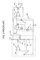
- FIG. 4is a diagram illustrating a voltage regulator including the conventional low pass filter circuit.
- the voltage regulator including the conventional low pass filter circuitincludes a ground terminal 100 , a power supply terminal 101 , an output terminal 102 , a low pass filter circuit 403 , an amplifier 105 , an output transistor 106 , and a reference voltage generation circuit 407 (see, for example, U.S. Pat. No. 7,397,226).
- an amplifier 104controls a voltage of a gate terminal of a PMOS transistor 120 so that an output voltage Vref of a reference voltage source 108 and a divided voltage Vfb obtained by dividing the output voltage Vref by resistors 151 and 152 are equal to each other.
- Vfb and Vrefare equal to each other, and hence, when the resistance values of the resistor 151 and 152 are represented by R 1 and R 2 , respectively, a voltage Vref 2 of a drain terminal of the PMOS transistor 120 is determined by a voltage dividing ratio of R 1 and R 2 as expressed by Expression (1)
- Vref2Vref ⁇ ( R 1 +R 2)/ R 2 (1)
- the resistance ratiocan be set relatively accurately, and hence, by adjusting the resistance ratio of the resistors 151 and 152 , the voltage Vref 2 can be accurately set to an arbitrary value.
- a voltage of an input terminal 112 and a voltage of an output terminal 113 of the low pass filter circuit 403are equal to each other in the steady state, and hence a voltage of the an inverting input terminal of the amplifier 105 is equal to the reference voltage Vref 2 .
- the amplifier 105controls a voltage of a gate terminal of the output transistor 106 so that the voltage of the output terminal 113 of the low pass filter circuit 403 and a voltage Vout of the output terminal 102 of the voltage regulator are equal to each other. Therefore, the output voltage Vout becomes equal to Vref 2 .
- Vref 2is determined by the resistance ratio of the resistors 151 and 152 , and hence the output voltage Vout can be arbitrarily adjusted through the adjustment of the resistance ratio of the resistors.
- a current source 111is designed so as to cause a very small current I 1 of, for example, about sub-nA to several nA, to flow.
- the current I 1is equal to a drain current of a PMOS transistor 122 , and hence the PMOS transistor 122 operates in the weak inversion region and has a very large ON-state resistance of, for example, about several hundreds of M ⁇ .
- An ON-state resistance Ron of a PMOS transistor 121 which is current-mirror connected to the PMOS transistor 122is similarly very large.
- a cutoff frequency fc of a low pass filter determined by the ON-state resistance Ron and a capacitor 161is very low.
- the low pass filter circuit 403suppresses 1/f noise which is contained in the reference voltage Vref 2 and generated in the reference voltage generation circuit 407 and thermal noise which is generated in the resistor voltage dividing circuit of the resistors 151 and 152 . Thus, smaller noise appears in the output terminal 102 . Therefore, a voltage regulator with small output noise can be obtained.
- the output voltageshifts due to a substrate leakage current of the PMOS transistor.
- thermo-stimulated currentflows in the forward direction of the diodes.
- the thermo-stimulated currentincreases exponentially with an increase in temperature, and hence the forward current becomes larger at a higher temperature.
- holesflow into the n-type conductive well due to the forward current.
- the holes flowing into the n-type conductive wellflow to the ground via a parasitic reverse diode formed between the well and a p-type conductive substrate, or alternatively the holes are recombined with electrons as major carriers in the n-type conductive well and disappear to generate a recombination current, which becomes a substrate leakage current in total.
- a potential difference between the channel region and the wellbecomes smaller than a potential difference between the source and the well, and hence the substrate leakage current from the channel region increases.
- the potential of the input terminal of the low pass filterthat is, the source potential of the PMOS transistor of the low pass filter is controlled to be constant.
- the potentials of the channel and the drainare decreased.
- the output voltage of the low pass filter circuitdecreases, and hence the output voltage of the voltage regulator also decreases along with the operation of the voltage regulator.
- a back gate terminal of a PMOS transistor in a low pass filter circuitis fixed to a potential higher than a source of the PMOS transistor. Further, in a voltage regulator incorporating the low pass filter circuit, the back gate terminal potential is generated by an existing reference voltage circuit or voltage dividing circuit.
- the voltage regulator including the low pass filter circuit of the present inventiona leakage current in the low pass filter circuit at high temperature is small, and hence the accuracy of an output voltage under a high temperature environment is improved as compared with conventional one.
- the back gate potential of the PMOS transistor in the low pass filter circuitis generated by an existing circuit provided in a low noise voltage regulator circuit, and hence it is unnecessary to provide a dedicated circuit for generating the back gate potential.
- the chip area of an ICis hardly increased, and the manufacturing cost is not increased.
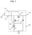
- FIG. 1is a circuit diagram illustrating a low pass filter circuit according to an embodiment of the present invention
- FIG. 2is a circuit diagram illustrating a voltage regulator including the low pass filter circuit according to the embodiment of the present invention
- FIG. 3is a circuit diagram illustrating anther voltage regulator including a low pass filter circuit according to the embodiment of the present invention.
- FIG. 4is a circuit diagram illustrating a voltage regulator including a conventional low pass filter circuit.
- FIG. 1is a diagram illustrating a low pass filter circuit according to the present invention.
- a low pass filter circuit 103includes PMOS transistors 121 and 122 , a current source 111 , a capacitor 161 , an input terminal 112 , a back gate input terminal 114 , and an output terminal 113 .
- the PMOS transistors 121 and 122each have a source terminal connected to the input terminal 112 , a substrate terminal connected to the back gate input terminal 114 , and a gate terminal connected to one terminal of the current source 111 and to a drain terminal of the PMOS transistor 122 .
- the other terminal of the current source 111is connected to a ground terminal 100 .
- the PMOS transistor 121has a drain terminal connected to the output terminal 113 and to one terminal of the capacitor 161 .
- the other terminal of the capacitor 161is connected to the ground terminal.
- a back gate voltage source 109is connected between the input terminal 112 and the back gate input terminal 114 .
- the present inventionis different from the conventional technology in that the back gate terminals of the PMOS transistors 121 and 122 are higher in potential than the source terminals.
- Vcw between the channel and the n-type conductive wellis large, and hence the leakage current is small.
- the leakage currentis small, almost no potential difference is generated between input and output terminals of a low pass filter circuit.
- an effect that almost no shift occurs in output voltage of the low pass filter circuitcan be obtained.
- a resistor or a low pass filter circuitmay be connected between the voltage source 109 and the back gate terminal of the PMOS transistor 121 .
- FIG. 2is a circuit diagram illustrating a voltage regulator including the above-mentioned low pass filter circuit according to an embodiment of the present invention.
- the voltage regulatorincludes the ground terminal 100 , a power supply terminal 101 , an output terminal 102 , the low pass filter circuit 103 , an amplifier 105 , an output transistor 106 , and a reference voltage generation circuit 107 .
- the reference voltage generation circuit 107includes a reference voltage source 108 , an amplifier 104 , a PMOS transistor 120 , and resistors 151 , 152 , and 153 .
- the PMOS transistor 120has a source connected to the power supply terminal 101 and a drain connected to one terminal of the resistor 153 .
- the other terminal of the resistor 153is connected in series to the resistor 151 .
- the resistor 151is grounded via the resistor 152 which is further connected in series.
- a node between the resistor 153 and the resistor 151is connected to the input terminal 112 of the low pass filter circuit 103 , and a node between the PMOS transistor 120 and the resistor 153 is connected to the input terminal 114 of the low pass filter circuit 103 .
- a voltage generated across the resistor 153corresponds to a source-back gate terminal voltage of the PMOS transistors 121 and 122 in the low pass filter circuit 103 .
- the use of the configuration of the voltage regulator in this embodimentcan suppress the leakage current of the low pass filter circuit at high temperature, thus preventing the decrease in output voltage of the low noise voltage regulator. Further, the back gate potential of the PMOS transistor of the low pass filter circuit is generated by resistor division in the reference voltage generation circuit 107 . Thus, it is unnecessary to add a dedicated circuit for generating the back gate voltage, and hence the increase in chip area can be suppressed, which does not affect manufacturing cost.
- FIG. 3is a circuit diagram illustrating a voltage regulator including a low pass filter circuit according to a second embodiment of the present invention.
- the voltage regulator according to the second embodimentincludes the low pass filter circuit 103 , the amplifier 105 , the output transistor 106 , and a reference voltage generation circuit 307 .
- the reference voltage generation circuit 307is an ED type reference voltage circuit, and includes NMOS depletion transistors 123 and 124 and an NMOS enhancement transistor 125 .
- the NMOS enhancement transistor 125has a source terminal connected to the ground terminal, and a gate terminal and a drain terminal connected to the input terminal 112 of the low pass filter circuit 103 .
- the NMOS depletion transistor 124has a source terminal and a gate terminal connected to the drain terminal of the NMOS enhancement transistor 125 and to a gate terminal of the NMOS depletion transistor 123 .
- the NMOS depletion transistor 124has a drain terminal connected to a source terminal of the NMOS depletion transistor 123 and to the back gate input terminal 114 of the low pass filter circuit 103 .
- the NMOS depletion transistor 123has a drain terminal connected to the power supply terminal 101 .
- a potential difference generated across the NMOS depletion transistor 124corresponds to a source-back gate terminal voltage of the PMOS transistors in the low pass filter circuit 103 .
- the series-connected NMOS depletion transistors 123 and 124are originally formed of a single element, if those transistors are not intended to be connected to the back gate input terminal 114 . Therefore, the element layout is different because the elements are divided, which however hardly contributes to an increased chip area.
- 1/f noiseis generated in the NMOS enhancement transistor and the NMOS depletion transistors, which is a primary factor of output noise of the voltage regulator.
- the configuration of FIG. 3can suppress the 1/f noise by the low pass filter circuit 103 .
Landscapes
- Engineering & Computer Science (AREA)
- Physics & Mathematics (AREA)
- Electromagnetism (AREA)
- General Physics & Mathematics (AREA)
- Radar, Positioning & Navigation (AREA)
- Automation & Control Theory (AREA)
- Continuous-Control Power Sources That Use Transistors (AREA)
Abstract
Description
Vref2=Vref·(R1+R2)/R2 (1)
P=P0·exp{−Vcw/(Kb·T)} (2)
where P0 represents a normalization constant, T represents temperature, Kb represents the Boltzmann constant, and Vcw represents a potential difference between the channel and the n-type conductive well. From Expression (2), the probability of thermal excitation becomes higher at a higher temperature and a lower Vcw, and a leakage current becomes larger in proportion to the probability P of Expression (2). In the circuit of the present invention, Vcw between the channel and the n-type conductive well is large, and hence the leakage current is small. When the leakage current is small, almost no potential difference is generated between input and output terminals of a low pass filter circuit. Thus, an effect that almost no shift occurs in output voltage of the low pass filter circuit can be obtained.
Claims (4)
Applications Claiming Priority (2)
| Application Number | Priority Date | Filing Date | Title |
|---|---|---|---|
| JP2012-054844 | 2012-03-12 | ||
| JP2012054844AJP5952035B2 (en) | 2012-03-12 | 2012-03-12 | Low pass filter circuit and voltage regulator |
Publications (2)
| Publication Number | Publication Date |
|---|---|
| US20130234688A1 US20130234688A1 (en) | 2013-09-12 |
| US8922188B2true US8922188B2 (en) | 2014-12-30 |
Family
ID=49113517
Family Applications (1)
| Application Number | Title | Priority Date | Filing Date |
|---|---|---|---|
| US13/779,253Expired - Fee RelatedUS8922188B2 (en) | 2012-03-12 | 2013-02-27 | Low pass filter circuit and voltage regulator |
Country Status (5)
| Country | Link |
|---|---|
| US (1) | US8922188B2 (en) |
| JP (1) | JP5952035B2 (en) |
| KR (1) | KR101956933B1 (en) |
| CN (1) | CN103309389B (en) |
| TW (1) | TWI590583B (en) |
Cited By (3)
| Publication number | Priority date | Publication date | Assignee | Title |
|---|---|---|---|---|
| US20180039296A1 (en)* | 2016-08-02 | 2018-02-08 | Sii Semiconductor Corporation | Voltage regulator |
| US11616505B1 (en)* | 2022-02-17 | 2023-03-28 | Qualcomm Incorporated | Temperature-compensated low-pass filter |
| US12445113B2 (en)* | 2023-01-31 | 2025-10-14 | Ablic Inc. | Low pass filter and semiconductor device |
Families Citing this family (13)
| Publication number | Priority date | Publication date | Assignee | Title |
|---|---|---|---|---|
| CN104714584B (en)* | 2013-12-13 | 2016-04-06 | 芯视达系统公司 | There is voltage regulator and the control method thereof of multi output scope |
| US10156860B2 (en)* | 2015-03-31 | 2018-12-18 | Skyworks Solutions, Inc. | Pre-charged fast wake up low-dropout regulator |
| US9625926B1 (en)* | 2015-11-18 | 2017-04-18 | Qualcomm Incorporated | Multiple input regulator circuit |
| US10574212B2 (en)* | 2017-11-21 | 2020-02-25 | Mediatek Inc. | Method and circuit for low-noise reference signal generation |
| TWI829663B (en)* | 2018-01-19 | 2024-01-21 | 日商半導體能源研究所股份有限公司 | Semiconductor device and operating method thereof |
| JP7000187B2 (en)* | 2018-02-08 | 2022-01-19 | エイブリック株式会社 | Reference voltage circuit and semiconductor device |
| CN108459649A (en)* | 2018-03-13 | 2018-08-28 | 李启同 | A kind of low-dropout regulator and multiple-way supply device of high stability |
| CN114460994B (en)* | 2020-11-09 | 2024-09-27 | 扬智科技股份有限公司 | Voltage Regulator |
| TWI800223B (en)* | 2021-11-17 | 2023-04-21 | 香港商科奇芯有限公司 | Low-pass filter circuit |
| US11909369B2 (en)* | 2021-11-17 | 2024-02-20 | Gutschsemi Limited | Low-pass filter circuit |
| CN114489215B (en)* | 2022-04-06 | 2022-07-08 | 江苏长晶科技股份有限公司 | Low-noise reference circuit and low-dropout linear voltage stabilizing circuit thereof |
| US12388420B2 (en) | 2022-06-01 | 2025-08-12 | Mediatek Inc. | Noise filter circuit with controllable transistor off-resistance and associated noise filtering method |
| CN119916880B (en)* | 2025-04-03 | 2025-06-17 | 成都芯翼科技有限公司 | A circuit to improve the power supply rejection ratio of LDO |
Citations (6)
| Publication number | Priority date | Publication date | Assignee | Title |
|---|---|---|---|---|
| JPH05127761A (en) | 1991-10-31 | 1993-05-25 | Fujitsu Ltd | Stabilized power supply circuit |
| US7397226B1 (en) | 2005-01-13 | 2008-07-08 | National Semiconductor Corporation | Low noise, low power, fast startup, and low drop-out voltage regulator |
| US20100007428A1 (en)* | 2006-06-09 | 2010-01-14 | Thine Electronics, Inc. | Oscillation circuit |
| US20100329157A1 (en)* | 2009-06-25 | 2010-12-30 | Nanoamp Solutions Inc. (Cayman) | Even-Order Harmonics Calibration |
| US20110032647A1 (en)* | 2006-05-31 | 2011-02-10 | Nec Electronics Corporation | Semiconductor device including esd protection field effect transistor with adjustable back gate potential |
| US8477159B2 (en)* | 2010-09-21 | 2013-07-02 | Lapis Semiconductor Co., Ltd. | Offset cancel output circuit of source driver for driving liquid crystal display |
Family Cites Families (8)
| Publication number | Priority date | Publication date | Assignee | Title |
|---|---|---|---|---|
| US5999043A (en)* | 1996-12-19 | 1999-12-07 | Texas Instruments Incorporated | On-chip high resistance device for passive low pass filters with programmable poles |
| US6522114B1 (en)* | 2001-12-10 | 2003-02-18 | Koninklijke Philips Electronics N.V. | Noise reduction architecture for low dropout voltage regulators |
| JP2004094788A (en)* | 2002-09-03 | 2004-03-25 | Seiko Instruments Inc | Voltage regulator |
| CN100373281C (en)* | 2003-06-05 | 2008-03-05 | 联发科技股份有限公司 | Low-noise fast and stable voltage stabilizing circuit |
| JP4804156B2 (en)* | 2006-02-01 | 2011-11-02 | 株式会社リコー | Constant voltage circuit |
| CN101459378B (en)* | 2007-12-14 | 2011-03-09 | 英业达股份有限公司 | Linear Buck Regulator |
| JP5446529B2 (en)* | 2009-07-14 | 2014-03-19 | 株式会社リコー | Low pass filter circuit, constant voltage circuit using the low pass filter circuit, and semiconductor device |
| JP5438477B2 (en)* | 2009-11-26 | 2014-03-12 | トレックス・セミコンダクター株式会社 | Reference voltage circuit |
- 2012
- 2012-03-12JPJP2012054844Apatent/JP5952035B2/ennot_activeExpired - Fee Related
- 2013
- 2013-02-27USUS13/779,253patent/US8922188B2/ennot_activeExpired - Fee Related
- 2013-03-04TWTW102107487Apatent/TWI590583B/ennot_activeIP Right Cessation
- 2013-03-07KRKR1020130024387Apatent/KR101956933B1/ennot_activeExpired - Fee Related
- 2013-03-12CNCN201310078000.9Apatent/CN103309389B/ennot_activeExpired - Fee Related
Patent Citations (6)
| Publication number | Priority date | Publication date | Assignee | Title |
|---|---|---|---|---|
| JPH05127761A (en) | 1991-10-31 | 1993-05-25 | Fujitsu Ltd | Stabilized power supply circuit |
| US7397226B1 (en) | 2005-01-13 | 2008-07-08 | National Semiconductor Corporation | Low noise, low power, fast startup, and low drop-out voltage regulator |
| US20110032647A1 (en)* | 2006-05-31 | 2011-02-10 | Nec Electronics Corporation | Semiconductor device including esd protection field effect transistor with adjustable back gate potential |
| US20100007428A1 (en)* | 2006-06-09 | 2010-01-14 | Thine Electronics, Inc. | Oscillation circuit |
| US20100329157A1 (en)* | 2009-06-25 | 2010-12-30 | Nanoamp Solutions Inc. (Cayman) | Even-Order Harmonics Calibration |
| US8477159B2 (en)* | 2010-09-21 | 2013-07-02 | Lapis Semiconductor Co., Ltd. | Offset cancel output circuit of source driver for driving liquid crystal display |
Cited By (4)
| Publication number | Priority date | Publication date | Assignee | Title |
|---|---|---|---|---|
| US20180039296A1 (en)* | 2016-08-02 | 2018-02-08 | Sii Semiconductor Corporation | Voltage regulator |
| US10007282B2 (en)* | 2016-08-02 | 2018-06-26 | Ablic Inc. | Voltage regulator |
| US11616505B1 (en)* | 2022-02-17 | 2023-03-28 | Qualcomm Incorporated | Temperature-compensated low-pass filter |
| US12445113B2 (en)* | 2023-01-31 | 2025-10-14 | Ablic Inc. | Low pass filter and semiconductor device |
Also Published As
| Publication number | Publication date |
|---|---|
| US20130234688A1 (en) | 2013-09-12 |
| KR20130105394A (en) | 2013-09-25 |
| CN103309389B (en) | 2016-12-28 |
| TW201401769A (en) | 2014-01-01 |
| CN103309389A (en) | 2013-09-18 |
| KR101956933B1 (en) | 2019-03-11 |
| TWI590583B (en) | 2017-07-01 |
| JP2013190855A (en) | 2013-09-26 |
| JP5952035B2 (en) | 2016-07-13 |
Similar Documents
| Publication | Publication Date | Title |
|---|---|---|
| US8922188B2 (en) | Low pass filter circuit and voltage regulator | |
| US7994764B2 (en) | Low dropout voltage regulator with high power supply rejection ratio | |
| US7646574B2 (en) | Voltage regulator | |
| US12282351B2 (en) | Bandgap reference circuit | |
| JP2019174976A (en) | Voltage regulator | |
| US7990207B2 (en) | Constant voltage circuit, constant voltage supply system and constant voltage supply method | |
| CN115562424A (en) | Integrated circuit and semiconductor module | |
| US20130002228A1 (en) | Current source with low power consumption and reduced on-chip area occupancy | |
| US11835979B2 (en) | Voltage regulator device | |
| US7965125B2 (en) | Current drive circuit | |
| US12032396B2 (en) | Voltage generating circuit and semiconductor device for suppressing leakage current | |
| JP6045148B2 (en) | Reference current generation circuit and reference voltage generation circuit | |
| JP6672067B2 (en) | Stabilized power supply circuit | |
| US10509430B2 (en) | Reference circuits | |
| CN108628379B (en) | Bias circuit | |
| JP2005122753A (en) | Temperature detection circuit, heating protection circuit, and various electronic devices incorporating these circuits | |
| US8791750B2 (en) | Constant voltage constant current generation circuit | |
| US12271218B2 (en) | Reference current circuit | |
| JP2024168601A (en) | Constant voltage generation circuit | |
| JP2011150547A (en) | Constant voltage output circuit | |
| CN116348830A (en) | Integrated circuit and semiconductor module | |
| JP2021101456A (en) | Electrostatic protection circuit and semiconductor device | |
| HK1143432B (en) | Low dropout (ldo) voltage regulator and method thereof |
Legal Events
| Date | Code | Title | Description |
|---|---|---|---|
| AS | Assignment | Owner name:SEIKO INSTRUMENTS INC., JAPAN Free format text:ASSIGNMENT OF ASSIGNORS INTEREST;ASSIGNOR:SAKAGUCHI, KAORU;REEL/FRAME:029890/0023 Effective date:20130208 | |
| FEPP | Fee payment procedure | Free format text:PAYOR NUMBER ASSIGNED (ORIGINAL EVENT CODE: ASPN); ENTITY STATUS OF PATENT OWNER: LARGE ENTITY | |
| STCF | Information on status: patent grant | Free format text:PATENTED CASE | |
| AS | Assignment | Owner name:SII SEMICONDUCTOR CORPORATION ., JAPAN Free format text:ASSIGNMENT OF ASSIGNORS INTEREST;ASSIGNOR:SEIKO INSTRUMENTS INC;REEL/FRAME:037783/0166 Effective date:20160209 | |
| AS | Assignment | Owner name:SII SEMICONDUCTOR CORPORATION, JAPAN Free format text:CORRECTIVE ASSIGNMENT TO CORRECT THE EXECUTION DATE PREVIOUSLY RECORDED AT REEL: 037783 FRAME: 0166. ASSIGNOR(S) HEREBY CONFIRMS THE ASSIGNMENT;ASSIGNOR:SEIKO INSTRUMENTS INC;REEL/FRAME:037903/0928 Effective date:20160201 | |
| AS | Assignment | Owner name:ABLIC INC., JAPAN Free format text:CHANGE OF NAME;ASSIGNOR:SII SEMICONDUCTOR CORPORATION;REEL/FRAME:045567/0927 Effective date:20180105 | |
| MAFP | Maintenance fee payment | Free format text:PAYMENT OF MAINTENANCE FEE, 4TH YEAR, LARGE ENTITY (ORIGINAL EVENT CODE: M1551) Year of fee payment:4 | |
| FEPP | Fee payment procedure | Free format text:MAINTENANCE FEE REMINDER MAILED (ORIGINAL EVENT CODE: REM.); ENTITY STATUS OF PATENT OWNER: LARGE ENTITY | |
| LAPS | Lapse for failure to pay maintenance fees | Free format text:PATENT EXPIRED FOR FAILURE TO PAY MAINTENANCE FEES (ORIGINAL EVENT CODE: EXP.); ENTITY STATUS OF PATENT OWNER: LARGE ENTITY | |
| STCH | Information on status: patent discontinuation | Free format text:PATENT EXPIRED DUE TO NONPAYMENT OF MAINTENANCE FEES UNDER 37 CFR 1.362 | |
| FP | Lapsed due to failure to pay maintenance fee | Effective date:20221230 |