US8921205B2 - Deposition of amorphous silicon-containing films - Google Patents
Deposition of amorphous silicon-containing filmsDownload PDFInfo
- Publication number
- US8921205B2 US8921205B2US11/626,730US62673007AUS8921205B2US 8921205 B2US8921205 B2US 8921205B2US 62673007 AUS62673007 AUS 62673007AUS 8921205 B2US8921205 B2US 8921205B2
- Authority
- US
- United States
- Prior art keywords
- film
- amorphous
- crystalline
- single crystal
- source
- Prior art date
- Legal status (The legal status is an assumption and is not a legal conclusion. Google has not performed a legal analysis and makes no representation as to the accuracy of the status listed.)
- Expired - Lifetime, expires
Links
Images


Classifications
- C—CHEMISTRY; METALLURGY
- C30—CRYSTAL GROWTH
- C30B—SINGLE-CRYSTAL GROWTH; UNIDIRECTIONAL SOLIDIFICATION OF EUTECTIC MATERIAL OR UNIDIRECTIONAL DEMIXING OF EUTECTOID MATERIAL; REFINING BY ZONE-MELTING OF MATERIAL; PRODUCTION OF A HOMOGENEOUS POLYCRYSTALLINE MATERIAL WITH DEFINED STRUCTURE; SINGLE CRYSTALS OR HOMOGENEOUS POLYCRYSTALLINE MATERIAL WITH DEFINED STRUCTURE; AFTER-TREATMENT OF SINGLE CRYSTALS OR A HOMOGENEOUS POLYCRYSTALLINE MATERIAL WITH DEFINED STRUCTURE; APPARATUS THEREFOR
- C30B29/00—Single crystals or homogeneous polycrystalline material with defined structure characterised by the material or by their shape
- C30B29/02—Elements
- C30B29/06—Silicon
- C—CHEMISTRY; METALLURGY
- C23—COATING METALLIC MATERIAL; COATING MATERIAL WITH METALLIC MATERIAL; CHEMICAL SURFACE TREATMENT; DIFFUSION TREATMENT OF METALLIC MATERIAL; COATING BY VACUUM EVAPORATION, BY SPUTTERING, BY ION IMPLANTATION OR BY CHEMICAL VAPOUR DEPOSITION, IN GENERAL; INHIBITING CORROSION OF METALLIC MATERIAL OR INCRUSTATION IN GENERAL
- C23C—COATING METALLIC MATERIAL; COATING MATERIAL WITH METALLIC MATERIAL; SURFACE TREATMENT OF METALLIC MATERIAL BY DIFFUSION INTO THE SURFACE, BY CHEMICAL CONVERSION OR SUBSTITUTION; COATING BY VACUUM EVAPORATION, BY SPUTTERING, BY ION IMPLANTATION OR BY CHEMICAL VAPOUR DEPOSITION, IN GENERAL
- C23C16/00—Chemical coating by decomposition of gaseous compounds, without leaving reaction products of surface material in the coating, i.e. chemical vapour deposition [CVD] processes
- C23C16/22—Chemical coating by decomposition of gaseous compounds, without leaving reaction products of surface material in the coating, i.e. chemical vapour deposition [CVD] processes characterised by the deposition of inorganic material, other than metallic material
- C23C16/24—Deposition of silicon only
- C—CHEMISTRY; METALLURGY
- C23—COATING METALLIC MATERIAL; COATING MATERIAL WITH METALLIC MATERIAL; CHEMICAL SURFACE TREATMENT; DIFFUSION TREATMENT OF METALLIC MATERIAL; COATING BY VACUUM EVAPORATION, BY SPUTTERING, BY ION IMPLANTATION OR BY CHEMICAL VAPOUR DEPOSITION, IN GENERAL; INHIBITING CORROSION OF METALLIC MATERIAL OR INCRUSTATION IN GENERAL
- C23C—COATING METALLIC MATERIAL; COATING MATERIAL WITH METALLIC MATERIAL; SURFACE TREATMENT OF METALLIC MATERIAL BY DIFFUSION INTO THE SURFACE, BY CHEMICAL CONVERSION OR SUBSTITUTION; COATING BY VACUUM EVAPORATION, BY SPUTTERING, BY ION IMPLANTATION OR BY CHEMICAL VAPOUR DEPOSITION, IN GENERAL
- C23C16/00—Chemical coating by decomposition of gaseous compounds, without leaving reaction products of surface material in the coating, i.e. chemical vapour deposition [CVD] processes
- C23C16/22—Chemical coating by decomposition of gaseous compounds, without leaving reaction products of surface material in the coating, i.e. chemical vapour deposition [CVD] processes characterised by the deposition of inorganic material, other than metallic material
- C23C16/30—Deposition of compounds, mixtures or solid solutions, e.g. borides, carbides, nitrides
- C23C16/32—Carbides
- C23C16/325—Silicon carbide
- C—CHEMISTRY; METALLURGY
- C30—CRYSTAL GROWTH
- C30B—SINGLE-CRYSTAL GROWTH; UNIDIRECTIONAL SOLIDIFICATION OF EUTECTIC MATERIAL OR UNIDIRECTIONAL DEMIXING OF EUTECTOID MATERIAL; REFINING BY ZONE-MELTING OF MATERIAL; PRODUCTION OF A HOMOGENEOUS POLYCRYSTALLINE MATERIAL WITH DEFINED STRUCTURE; SINGLE CRYSTALS OR HOMOGENEOUS POLYCRYSTALLINE MATERIAL WITH DEFINED STRUCTURE; AFTER-TREATMENT OF SINGLE CRYSTALS OR A HOMOGENEOUS POLYCRYSTALLINE MATERIAL WITH DEFINED STRUCTURE; APPARATUS THEREFOR
- C30B25/00—Single-crystal growth by chemical reaction of reactive gases, e.g. chemical vapour-deposition growth
- C30B25/02—Epitaxial-layer growth
- H—ELECTRICITY
- H01—ELECTRIC ELEMENTS
- H01L—SEMICONDUCTOR DEVICES NOT COVERED BY CLASS H10
- H01L21/00—Processes or apparatus adapted for the manufacture or treatment of semiconductor or solid state devices or of parts thereof
- H01L21/02—Manufacture or treatment of semiconductor devices or of parts thereof
- H01L21/02104—Forming layers
- H01L21/02365—Forming inorganic semiconducting materials on a substrate
- H01L21/02367—Substrates
- H01L21/0237—Materials
- H01L21/02373—Group 14 semiconducting materials
- H01L21/02378—Silicon carbide
- H—ELECTRICITY
- H01—ELECTRIC ELEMENTS
- H01L—SEMICONDUCTOR DEVICES NOT COVERED BY CLASS H10
- H01L21/00—Processes or apparatus adapted for the manufacture or treatment of semiconductor or solid state devices or of parts thereof
- H01L21/02—Manufacture or treatment of semiconductor devices or of parts thereof
- H01L21/02104—Forming layers
- H01L21/02365—Forming inorganic semiconducting materials on a substrate
- H01L21/02367—Substrates
- H01L21/0237—Materials
- H01L21/02373—Group 14 semiconducting materials
- H01L21/02381—Silicon, silicon germanium, germanium
- H—ELECTRICITY
- H01—ELECTRIC ELEMENTS
- H01L—SEMICONDUCTOR DEVICES NOT COVERED BY CLASS H10
- H01L21/00—Processes or apparatus adapted for the manufacture or treatment of semiconductor or solid state devices or of parts thereof
- H01L21/02—Manufacture or treatment of semiconductor devices or of parts thereof
- H01L21/02104—Forming layers
- H01L21/02365—Forming inorganic semiconducting materials on a substrate
- H01L21/02518—Deposited layers
- H01L21/02521—Materials
- H01L21/02524—Group 14 semiconducting materials
- H01L21/02529—Silicon carbide
- H—ELECTRICITY
- H01—ELECTRIC ELEMENTS
- H01L—SEMICONDUCTOR DEVICES NOT COVERED BY CLASS H10
- H01L21/00—Processes or apparatus adapted for the manufacture or treatment of semiconductor or solid state devices or of parts thereof
- H01L21/02—Manufacture or treatment of semiconductor devices or of parts thereof
- H01L21/02104—Forming layers
- H01L21/02365—Forming inorganic semiconducting materials on a substrate
- H01L21/02518—Deposited layers
- H01L21/02521—Materials
- H01L21/02524—Group 14 semiconducting materials
- H01L21/02532—Silicon, silicon germanium, germanium
- H—ELECTRICITY
- H01—ELECTRIC ELEMENTS
- H01L—SEMICONDUCTOR DEVICES NOT COVERED BY CLASS H10
- H01L21/00—Processes or apparatus adapted for the manufacture or treatment of semiconductor or solid state devices or of parts thereof
- H01L21/02—Manufacture or treatment of semiconductor devices or of parts thereof
- H01L21/02104—Forming layers
- H01L21/02365—Forming inorganic semiconducting materials on a substrate
- H01L21/02612—Formation types
- H01L21/02617—Deposition types
- H01L21/0262—Reduction or decomposition of gaseous compounds, e.g. CVD
Definitions
- This applicationrelates generally to the deposition of silicon-containing materials. More particularly, this application relates to the deposition of amorphous silicon-containing films using trisilane, and to the annealing of such films to form crystalline silicon-containing films over a variety of substrates, including mixed substrates. Such deposition processes are useful in a variety of applications, e.g., semiconductor manufacturing.
- Si-containingsilicon-containing
- CMOScomplementary metal-oxide-semiconductor
- Nucleationthe first stage, is very important and is greatly affected by the nature and quality of the substrate surface. Nucleation occurs as the first few atoms or molecules deposit onto the surface and form nuclei.
- the isolated nucleiform small islands that grow into larger islands.
- the growing islandsbegin coalescing into a continuous film.
- the filmtypically has a thickness of a few hundred angstroms and is known as a “transition” film. It generally has chemical and physical properties that are different from the thicker bulk film that begins to grow after the transition film is formed.
- Deposition processesare usually designed to produce a particular type of bulk film morphology, e.g., single crystal, epitaxial, polycrystalline or amorphous.
- nucleationis very important and critically dependent on substrate quality. For example, attempting to grow a single-crystal film on a wafer with islands of unremoved oxide will result in regions of polysilicon in the bulk film. Because of these nucleation issues, deposition of thin film Si-containing materials with similar physical properties onto substrates having two or more different types of surfaces using conventional silicon sources and deposition methods is often problematic.
- silicon tetrachloride (SiCl 4 ), silane (SiH 4 ) and dichlorosilane (SiH 2 Cl 2 )are the most widely used silicon sources in the semiconductor manufacturing industry for depositing Si-containing films, see Peter Van Zant, “Microchip Fabrication,” 4 th Ed., McGraw Hill, New York, (2000), p 380-382.
- deposition using these conventional silicon sourcesis generally difficult to control over mixed substrates, such as surfaces containing both single crystal silicon and silicon dioxide. Control is difficult because the morphology and thickness of the resulting Si-containing film depend on both the deposition temperature and the morphology of the underlying substrate.
- 4,578,142discloses that the deposition of single crystal silicon onto a single crystal surface using SiH 2 Cl 2 begins immediately, whereas there is a delay before non-single-crystalline deposition occurs on an adjoining silicon dioxide surface.
- Other deposition parametersincluding total reactor pressure, reactant partial pressure and reactant flow rate can also strongly influence the quality of depositions over mixed substrates.
- U.S. Pat. No. 4,578,142discloses the use of a two stage silicon deposition/etching cycle that involves depositing single crystal silicon onto a single crystal surface and selectively etching to remove any non-single crystalline material, then repeating the cycle until the deposited single crystal silicon grows laterally across an adjoining silicon dioxide surface.
- Later patentsrefer to this deposition process as “epitaxial lateral overgrowth” (“ELO”), see U.S. Pat. Nos. 4,615,762; 4,704,186; and 4,891,092. Similar ELO techniques are disclosed in U.S. Pat. Nos. 4,557,794 and 4,755,481.
- ELOprovides a method for depositing single crystal silicon over portions of an adjoining non-single crystalline surface, the ability to extend the single crystal over large areas is limited.
- Solid phase epitaxyis the solid phase transformation of an amorphous Si-containing material to single crystal Si-containing material, see U.S. Pat. Nos. 4,509,990; 4,808,546; 4,975,387; and 5,278,903. SPE has been used to selectively form single crystalline silicon over semiconductor substrates.
- U.S. Pat. No. 6,346,732discloses depositing an amorphous silicon film over a mixed substrate having a semiconductor surface and a silicon nitride surface by low pressure chemical vapor deposition (“LPCVD”) using silane as a deposition gas, then transforming the portion of the amorphous film over the semiconductor surface to single crystalline silicon by annealing.
- LPCVDlow pressure chemical vapor deposition
- U.S. Pat. No. 6,346,732discloses that the portion of the amorphous silicon film over the silicon nitride surface remained amorphous after annealing, see column 18, lines 47-58.
- JP Patent Application No. 63166502discloses depositing an amorphous silicon film over a mixed substrate having a single crystal silicon surface and a silicon dioxide surface by LPCVD using silane as a deposition gas, then transforming the amorphous film over both of the underlying surfaces to single crystalline silicon by annealing.
- This processapparently proceeds by a lateral overgrowth mechanism, in which the annealing initiates crystallization of the amorphous film in the portion of the amorphous film over the single crystal silicon surface.
- the portion of the amorphous silicon layer overlying the non-single crystal surface and adjoining the newly crystallized regionis then transformed into single-crystal silicon by lateral overgrowth, see JP Application No. 60257703 and U.S. Pat. No. 6,274,463. Crystallization of amorphous silicon to form polycrystalline silicon can be initiated by the introduction of catalyst elements, see U.S. Pat. No. 6,162,667.
- FETdouble gate field effect transistors
- H.-S Wong“Beyond the Conventional MOFSET,” IEDM Technical Digest, and/or involves complicated processing steps, see U.S. Pat. Nos. 6,372,559 and 6,365,465.
- C. Edwards“Submicron zone catalyst for end of bulk CMOS,” EETimes, May 12, 2001.
- the fabrication complexitycan be traced to the multiple masking, deposition, etching, and planarization steps used to create various structures over assorted underlying surfaces, particularly those having mixed morphologies.
- a preferred embodimentprovides a deposition method comprising: providing a substrate disposed within a chamber, the substrate comprising a first surface having a first surface morphology and a second surface having a second surface morphology different from the first surface morphology; introducing trisilane to the chamber under chemical vapor deposition conditions; and depositing an amorphous Si-containing film onto the substrate over both of the first surface and the second surface.
- Another preferred embodimentprovides a deposition method comprising: depositing an amorphous Si-containing film onto a substrate using a feed gas that comprises trisilane; and annealing the amorphous Si-containing film to form a crystalline Si-containing film.
- FIGS. 1A and 1Bare schematic cross sections of the structures obtained by prior art methods for creating a single crystalline film overlying a mixed substrate.
- FIG. 1Aillustrates a film deposited using silane under deposition conditions resulting in the formation of a single crystal film over the single crystal portion of the mixed substrate.
- FIG. 1Billustrates a film deposited using silane under conditions resulting in the formation of an amorphous film over a mixed substrate, followed by annealing to form a single crystalline film over the single crystalline portion of the mixed substrate.
- FIG. 2schematically illustrates a process for depositing an amorphous Si-containing film over a mixed substrate using trisilane, then annealing to form a single crystal region over the underlying single crystal surface and a polycrystalline region over the underlying dielectric surface.
- FIG. 3schematically illustrates a process for depositing an amorphous Si-containing film over a mixed substrate using trisilane, then annealing to form a single crystal region over the underlying single crystal surface and over the underlying dielectric surface.
- FIG. 4schematically illustrates a process for depositing an amorphous Si-containing film over a dielectric substrate using trisilane, annealing to form a single crystal region over the underlying dielectric surface, then depositing a single crystal film over the single crystal region.
- FIG. 5schematically illustrates a process for depositing an amorphous Si-containing film over a single crystal substrate using trisilane, then annealing to form a single crystal region over the underlying single crystal surface.
- FIG. 1illustrates the results obtained by typical prior art deposition processes using silane as the silicon source
- FIGS. 2-5schematically illustrate preferred structures resulting from deposition using trisilane.
- FIGS. 2-5show that the trisilane deposition methods described herein may be used to provide an amorphous Si-containing film that can be annealed to produce high quality single crystal and/or polycrystalline films over a variety of substrates, including mixed substrates. The preferred embodiments illustrated in FIGS. 2-5 are discussed in greater detail below.
- a “mixed substrate”is a substrate that has two or more different types of surfaces.
- surfacescan be different from each other.
- the surfacescan be made from different elements such as copper or silicon, or from different metals, such as copper or aluminum, or from different Si-containing materials, such as silicon or silicon dioxide. Even if the materials are made from the same element, the surfaces can be different if the morphologies (crystallinity) of the surfaces are different.
- the electrical properties of surfacescan also make them different from each other.
- Si-containing layersare simultaneously formed over conductive and semiconductive materials and dielectrics. Examples of dielectric materials include silicon dioxide, silicon nitride, metal oxide and metal silicate.
- Such a mixed substratecomprises a first surface having a first surface morphology and a second surface having a second surface morphology.
- surface morphologyrefers to the crystalline structure of the substrate surface.
- Amorphous and crystallineare examples of different morphologies.
- Polycrystalline morphologyis a crystalline structure that consists of a disorderly arrangement of orderly crystals and thus has an intermediate degree of order. The atoms in a polycrystalline material have long range order within each of the crystals, but the crystals themselves lack long range order with respect to one another.
- Single crystal morphologyis a crystalline structure that has a high degree of order.
- Epitaxial filmsare characterized by a crystal structure and orientation that is identical to the substrate upon which they are grown. The atoms in these materials are arranged in a lattice-like structure that persists over relatively long distances (on an atomic scale), Amorphous morphology is a non-crystalline structure having a low degree of order because the atoms lack a definite periodic arrangement. Other morphologies include microcrystalline and mixtures of amorphous and crystalline material. As used herein, “single-crystal” or “epitaxial” is used to describe a predominantly large crystal structure that may have a tolerable number of faults therein.
- crystallinity of a layergenerally falls along a continuum from amorphous to polycrystalline to single-crystal; the skilled artisan can readily determine when a crystal structure can be considered single-crystal or epitaxial, despite low density faults.
- Specific examples of mixed substratesinclude without limitation single crystal/polycrystalline, single crystal/amorphous, epitaxial/polycrystalline, epitaxial/amorphous, single crystal/dielectric, epitaxial/dielectric, conductor/dielectric, and semiconductor/dielectric.
- mixed substrateincludes substrates having more than two different types of surfaces, and thus the skilled artisan will understand that methods described herein for depositing Si-containing films onto mixed substrates having two types of surfaces may also be applied to mixed substrates having three or more different types of surfaces.
- the delivery of trisilane to the surface of a substratepreferably results in the formation of an amorphous Si-containing film.
- delivery of the trisilane to the substrate surfaceis accomplished by introducing the trisilane to a suitable chamber having the substrate disposed therein.
- a high quality amorphous Si-containing filmcan be deposited onto the substrate over various surface types. Deposition may be suitably conducted according to the various CVD methods known to those skilled in the art, but the greatest benefits are obtained when deposition is conducted according to the CVD methods taught herein.
- the disclosed methodsmay be suitably practiced by employing CVD, including plasma-enhanced chemical vapor deposition (PECVD) or thermal CVD, utilizing gaseous trisilane to deposit an amorphous Si-containing film onto a substrate contained within a CVD chamber.
- CVDincluding plasma-enhanced chemical vapor deposition (PECVD) or thermal CVD, utilizing gaseous trisilane to deposit an amorphous Si-containing film onto a substrate contained within a CVD chamber.
- PECVDplasma-enhanced chemical vapor deposition
- thermal CVDutilizing gaseous trisilane to deposit an amorphous Si-containing film onto a substrate contained within a CVD chamber.
- thermal CVDis preferred.
- Trisilaneis preferably introduced to the chamber in the form of a gas or as a component of a feed gas.
- the total pressure in the CVD chamberis preferably in the range of about 0.001 Torr to about 1000 Torr, more preferably in the range of about 0.1 Torr to about 850 Torr, even more preferably in the range of about 1 Torr to about 350 Torr, most preferably in the range of about 1 Torr to about 100 torn.
- the partial pressure of trisilaneis preferably in the range of about 0.0001% to about 100% of the total pressure, more preferably about 0.001% to about 50% of the total pressure.
- the feed gascan also include a gas or gases other than trisilane, such as other silicon sources or inert carrier gases. Hydrogen and nitrogen are preferred carrier gases for the methods described herein.
- trisilaneis introduced to the chamber by way of a bubbler used with a carrier gas to entrain trisilane vapor, more preferably a temperature controlled bubbler.
- trisilaneis introduced to the chamber along with a hydrogen carrier gas, using a relatively high trisilane flow rate and a relatively low hydrogen flow rate, as compared to using silane in place of trisilane.
- thermal CVDis carried out in an Epsilon E2500TM reactor system (available commercially from ASM America, Inc., of Phoenix, Ariz.) using a trisilane flow rate of about 50 standard cubic centimeters per minute (sccm) or greater (bubbler), more preferably about 100 scem or greater, even more preferably about 200 sccm or greater, a hydrogen flow rate of about 25 standard liters per minute (slm) or less, more preferably about 20 slm or less, and at a deposition temperature in the range of about 350° C. to about 530° C.
- Thermal CVDis preferably conducted at a substrate temperature that is effective to deposit an amorphous Si-containing film over the substrate.
- thermal CVDis conducted at a temperature in the range of about 350° C. to about 530° C., more preferably about 400° C. to about 500° C., most preferably about 425° C. to about 475° C.
- PECVDis preferably conducted at a temperature in the range of about 0° C. to about 500° C.
- the substratecan be heated by a variety of methods known in the art, e.g., resistive heating and lamp heating.
- a suitable manifoldmay be used to supply feed gas(es) to the CVD chamber.
- the gas flow in the CVD chamberis horizontal, most preferably the chamber is a single-wafer, single pass, laminar horizontal gas flow reactor, preferably radiantly heated.
- Suitable reactors of this typeare commercially available, and preferred models include the EpsilonTM series of single wafer reactors commercially available from ASM America, Inc. of Phoenix, Ariz. While the methods described herein can also be employed in alternative reactors, such as a showerhead arrangement, benefits in increased uniformity and deposition rates have been found particularly effective in the horizontal, single-pass laminar gas flow arrangement of the EpsilonTM chambers, employing a rotating substrate, particularly with low process gas residence times.
- CVDmay be conducted by introducing plasma products (in situ or downstream of a remote plasma generator) to the chamber, but thermal CVD is preferred.
- the feed gasmay also contain other materials known by those skilled in the art to be useful for doping or alloying Si-containing films, as desired.
- the gasfurther comprises one or more precursors selected from the group consisting of silicon source, germanium source, carbon source, boron source, gallium source, indium source, arsenic source, phosphorous source, antimony source, nitrogen source and oxygen source.
- Specific examples of such sourcesinclude: silane, disilane and tetrasilane as silicon sources; germane, digermane and trigermane as germanium sources; NF 3 , ammonia, hydrazine and atomic nitrogen as nitrogen sources; various hydrocarbons, e.g., methane, ethane, propane, etc.
- Incorporation of dopants into Si-containing films by CVD using trisilaneis preferably accomplished by in situ doping using dopant precursors.
- Precursors for electrical dopantsinclude diborane, deuterated diborane, phosphine, arsenic vapor, and arsine.
- SbH 3 and trimethylindiumare preferred sources of antimony and indium, respectively.
- Such dopant precursorsare useful for the preparation of preferred films as described below, preferably boron-, phosphorous-, antimony-, indium-, and arsenic-doped silicon, SiC, SiGe and SiGeC films and alloys.
- SiCSiGe
- SiGeCrepresent materials that contain the indicated elements in various proportions.
- SiGeis a material that comprises silicon, germanium and, optionally, other elements, e.g., dopants.
- SiC”, “SiGe”, and “SiGeC”are not stoichiometric chemical formulas per se and thus are not limited to materials that contain particular ratios of the indicated elements.
- the amount of dopant precursor in the feed gasmay be adjusted to provide the desired level of dopant in the Si-containing film.
- Typical concentrations in the feed gascan be in the range of about 1 part per billion (ppb) to about 1% by weight based on total feed gas weight, although higher or lower amounts are sometimes preferred in order to achieve the desired property in the resulting film.
- dilute mixtures of dopant precursor in a carrier gascan be delivered to the reactor via a mass flow controller with set points ranging from about 10 to about 200 standard cubic centimeters per minute (seem), depending on desired dopant concentration and dopant gas concentration.
- the dilute mixtureis preferably further diluted by mixing with trisilane and any suitable carrier gas.
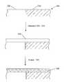
- FIGS. 1A and 1Bare schematic cross sections of typical structures obtained by prior art methods for creating a single crystal film overlying a mixed substrate.
- FIG. 1Aillustrates a film 110 deposited using silane under deposition conditions resulting in the formation of a single crystal film 120 over the single crystal portion 130 of the mixed substrate. It is apparent from FIG. 1A that the thickness of the deposited film is not uniform, because the nucleation rate of silane on the dielectric portion 140 of the underlying mixed substrate differs considerably from the nucleation rate on the single crystal portion 130 .
- FIG. 1Aillustrates a film 110 deposited using silane under deposition conditions resulting in the formation of a single crystal film 120 over the single crystal portion 130 of the mixed substrate. It is apparent from FIG. 1A that the thickness of the deposited film is not uniform, because the nucleation rate of silane on the dielectric portion 140 of the underlying mixed substrate differs considerably from the nucleation rate on the single crystal portion 130 .
- FIG. 1Aillustrates a film 110 deposited using
- FIG. 1Billustrates a film deposited using silane under conditions resulting in the formation of an amorphous film 150 over a mixed substrate, followed by annealing to form a single crystalline film 160 over the single crystal portion 170 of the mixed substrate. It is apparent that thickness uniformity is improved somewhat relative to FIG. 1A (because the deposition of amorphous films is less sensitive to the morphology of the substrate), but nevertheless remains a problem.
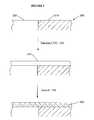
- FIG. 2schematically illustrates the deposition of an amorphous Si-containing film over a mixed substrate using trisilane, followed by annealing to form a film having both single crystal and polycrystalline regions.
- annealingmeans subjecting a Si-containing material to a thermal treatment that alters its degree of crystalline order.
- a mixed substrate 200 having a single crystal surface 210 and a dielectric surface 220is exposed to trisilane CVD conditions 230 to deposit an amorphous Si-containing film 240 over both the surfaces 210 and 220 .
- Preferred trisilane deposition conditionsinvolve introducing trisilane to a deposition chamber (not shown) having the mixed substrate 200 disposed therein, preferably at a deposition temperature in the range of about 350° C. to about 530° C., more preferably about 400° C. to about 500° C., most preferably about 425° C. to about 475° C., for a period of time that is effective to produce an amorphous Si-containing film having the desired thickness.
- Trisilaneis preferably delivered in the form of a feed gas to the chamber via a temperature controlled bubbler at a flow rate of about 50 sccm or greater, preferably in admixture with a carrier gas.
- the feed gasmay also contain other materials known by those skilled in the art to be useful for doping or alloying Si-containing films, as discussed above.
- the Si-containing filmis silicon, doped silicon, SiGe, or doped SiGe.
- the amorphous film 240is very uniform, as discussed below with respect to Table 1.
- the amorphous film 240is then annealed 250 at a temperature or temperatures in the range of about 500° C. to about 1100° C. to produce a mixed morphology crystalline film 260 having a single crystal region 270 over the single crystal surface 210 and a polycrystalline region 280 over the dielectric surface 220 . Within the range of about 500° C.
- annealing at lower temperaturestends to be slower and also tends to increase epitaxial lateral overgrowth (ELO) of the single crystal region 270 over the dielectric surface 220 , minimizing the polycrystalline region 280 , whereas annealing at higher temperatures tends to be faster and also minimizes ELO.
- annealing at higher temperaturesalso tends to consume thermal budget.
- annealingis conducted at a temperature or temperatures in the range of about 530° C. to about 750° C., more preferably about 550° C. to about 700° C., even more preferably about 575° C. to about 650° C., for a period of time that is effective to crystallize the amorphous film to the extent desired. Partial crystallization results in a film that comprises a mixture of amorphous and crystalline material.
- FIG. 3schematically illustrates the deposition of an amorphous film over a mixed substrate using trisilane, followed by annealing to form a film having a single crystal region that extends over both of the underlying surfaces.
- a mixed substrate 300 having a single crystal semiconductor surface 310 and a dielectric surface 320is exposed to trisilane CVD conditions 330 to deposit an amorphous Si-containing film 340 over both the surfaces 310 and 320 .
- Trisilane CVD conditions 330are generally similar to trisilane CVD conditions 230 described above.
- the amorphous Si-containing film 340is very uniform, as discussed below with respect to Table 1.
- the amorphous film 340is then annealed 350 at a temperature or temperatures in the range of about 500° C.
- annealingis conducted at a temperature or temperatures in the range of about 500° C. to about 700° C., more preferably about 530° C.
- Partial crystallizationresults in a film that comprises a mixture of amorphous and crystalline material.
- FIG. 4schematically illustrates the deposition of an amorphous film over an oxide substrate using trisilane.
- An oxide substrate 400is exposed to trisilane CVD conditions 410 to deposit an amorphous Si-containing film 420 thereon.
- Trisilane CVD conditions 410are generally similar to trisilane CVD conditions 230 described above.
- the amorphous film 420may then be annealed 430 at a temperature or temperatures in the range of about 500° C. to about 1100° C. to produce a single crystal film 440 .
- the resulting structure 450is a silicon-on-oxide (SOI) structure that is useful in a number of applications as described below.
- SOIsilicon-on-oxide
- Annealing at temperatures closer to 500° C.tends to be slower, but consumes less thermal budget.
- annealingis conducted at a temperature or temperatures in the range of about 500° C. to about 750° C., more preferably about 530° C. to about 700° C., even more preferably about 550° C. to about 650° C., for a period of time that is effective to crystallize the amorphous film to the extent desired. Partial crystallization results in a film that comprises a mixture of amorphous and crystalline material.
- the SOI structure 450is a preferred embodiment useful in a number of applications.
- FIG. 4illustrates a process in which the structure 450 serves as a substrate for a deposition step 460 that results in an single crystal SiGe film 470 overlying single crystal film 440 .
- the deposition step 460may be conducted by any method known to those skilled in the art for depositing single crystal SiGe films over single crystal substrates, but is preferably conducted using trisilane as the silicon source.
- the deposition step 460may be conducted by directly depositing the single crystal SiGe film 470 onto the single crystal film 440 , optionally after preparing the epitaxial film 440 for deposition using an HF last clean and/or bake step.
- the deposition step 460is preferably conducted in the general manner described below with respect to FIG. 5 for depositing the single crystal film 540 onto the single crystal substrate 500 .
- FIG. 5schematically illustrates the deposition of an amorphous film over a single crystal substrate using trisilane.
- a single crystal substrate 500is exposed to trisilane CVD conditions 510 to deposit an amorphous Si-containing film 520 thereon.
- Trisilane CVD conditions 510are generally similar to trisilane CVD conditions 230 described above.
- the amorphous film 520may then be annealed 530 at a temperature or temperatures in the range of about 500° C. to about 1100° C. to produce a single crystal film 540 . Annealing at temperatures closer to 500° C. tends to be slower, but also tends to produce single crystal films having fewer faults and consumes less thermal budget.
- annealingis conducted at a temperature or temperatures in the range of about 500° C. to about 750° C., more preferably about 530° C. to about 700° C., even more preferably about 550° C. to about 650° C., for a period of time that is effective to crystallize the amorphous film to the extent desired. Partial crystallization results in a film that comprises a mixture of amorphous and crystalline material.
- deposition of amorphous Si-containing films using trisilanecan offer significant advantages over the use of conventional silicon sources when conducted as described herein.
- deposition of Si-containing films using trisilanepreferably proceeds at a rate that is significantly faster than when silane is used instead of trisilane.
- Deposition of the amorphous Si-containing films described hereinis preferably conducted at a rate of about 5 ⁇ per minute or higher, more preferably about 10 ⁇ per minute or higher, most preferably about 20 ⁇ per minute or higher.
- a preferred embodimentprovides a high rate deposition method in which trisilane is delivered to the substrate surface at a delivery rate of at least about 0.001 milligram per minute per square centimeter of the substrate surface, more preferably at least about 0.003 milligram per minute per square centimeter of the substrate surface.
- a delivery rateof at least about 0.001 milligram per minute per square centimeter of the substrate surface, more preferably at least about 0.003 milligram per minute per square centimeter of the substrate surface.
- the Si-containing materialpreferably at a deposition temperature in the range of about 425° C. to about 525° C.
- practice of this embodimentresults in relatively fast deposition of the Si-containing material (as compared to other silicon sources), preferably at a rate of about 10 ⁇ per minute or higher, more preferably about 25 ⁇ per minute or higher, most preferably about 50 ⁇ per minute or higher.
- a germanium sourceis also delivered to the surface along with the trisilane to thereby deposit a SiG
- Preferred amorphous Si-containing filmshave a thickness that is highly uniform across the surface of the film.
- the percent thickness non-uniformity for the resulting amorphous filmsis preferably about 20% or less.
- additional values for percent thickness non-uniformitymay be preferred as shown in Table 1 below. Each value for % thickness non-uniformity shown in Table 1 is to be understood as if preceded by the word “about.”
- measurements of film thickness uniformity for a film deposited under a particular set of process conditionscan be made by depositing the film on a uniform or mixed substrate having a diameter in the range of about 200 mm to about 300 mm.
- Film thickness uniformityis determined by making multiple-point thickness measurements along a randomly selected diameter (with no measurements being taken within a 3 mm exclusion zone at the wafer periphery), determining the mean thickness by averaging the various thickness measurements, and determining the root mean square (rms) variability.
- a preferred instrument for measuring film thicknessutilizes a Nanospec® 8300 ⁇ SE instrument (commercially available from Nanometrics, Inc., Sunnyvale, Calif.), and a preferred measurement method involves using such an instrument to measure the film thickness at 49 points along a randomly selected wafer diameter.
- thickness variabilityis typically obtained directly from the instrument following such a measurement, and thus need not be calculated manually.
- the resultscan be expressed as percent non-uniformity, calculated by dividing the rms thickness variability by the mean thickness and multiplying by 100 to express the result as a percentage.
- the filmWhen measuring thickness uniformity of a film having a surface that is not accessible to such a measurement, e.g., a film onto which one or more additional layers have been applied, or a film contained within an integrated circuit, the film is cross sectioned and examined by electron microscopy. The film thickness is measured at the thinnest part of the cross sectioned film and at the thickest part, and the range in thickness measurements (e.g., ⁇ 6 ⁇ ) between these two points is then divided by the sum of the two measurements. This non-uniformity is expressed as a percentage herein.
- the annealing temperature or temperature rangeis preferably selected by considering factors such as the desired degree and type of crystallinity, the rate of production, and/or the thermal budget for the process, and is typically in the range of about 500° C. to about 1100° C., preferably in the range of about 530° C. to about 750° C., and more preferably about 525° C. to about 650° C.
- the degree of crystalline order achieved by annealingmay be affected by the time, temperature and pressure during annealing, and by the thickness of the amorphous film. For example, the rate of annealing is generally faster at higher temperatures and at lower pressures. Longer annealing times and/or lower pressures tend to produce higher degrees of crystallinity. Thinner amorphous films tend to crystallize more quickly and to a greater extent than thicker films.
- the temperature and/or the pressuremay be held constant or varied over the course of annealing.
- the use of trisilane as described herein to deposit amorphous Si-containing filmsenables the efficient production of a variety of crystalline films by annealing the deposited films.
- the overall production rate of a crystalline filmmay be materially increased by using trisilane to deposit the precursor amorphous film more quickly; a crystalline film having a mixed morphology can be produced by using trisilane to deposit the amorphous precursor film over a mixed substrate; and/or the thickness uniformity of a crystalline film may be improved by using trisilane to deposit a correspondingly uniform amorphous precursor film.
- the percent thickness non-uniformity for the resulting crystalline filmsis preferably about 20% or less.
- additional values for percent thickness non-uniformitymay be preferred as shown in Table 1 above.
- compositional uniformity of preferred crystalline Si-containing films that contain other elementsmade in accordance with the methods described herein, e.g., depositing an amorphous film using trisilane and a source of the other element, then annealing to crystallize, is materially improved as compared to corresponding films made without the use of trisilane.
- This inventionis not bound by any theory of operation, but it is believed that the amorphous Si-containing films have a degree of compositional uniformity that is better than corresponding as-deposited crystalline Si-containing films, and that this degree of compositional uniformity is substantially preserved when the amorphous films are annealed.
- crystalline Si-containing alloys containing relatively high levels of non-silicon element(s)can be prepared by the methods described herein.
- crystalline SiGepreferably contains about 10 atomic % Ge or greater, more preferably about 20 atomic % Ge or greater, even more preferably about 30 atomic % Ge or greater.
- preferred embodimentsprovide improved crystalline Si-containing films by using trisilane to deposit an amorphous precursor film, then annealing the precursor film by, e.g., SPE or ELO to form a crystalline film.
- the ability to deposit precursor amorphous films quickly and with a high degree of uniformity, even when the films are thin and even over mixed substrates,enables corresponding improvements in the production and quality of the resulting crystalline films.
- the use of trisilaneis especially useful in SPE and ELO processes, as compared to the use of conventional silicon sources, because it enables the processes to be conducted faster and/or results in the production of higher quality crystalline films.
- a relatively thick, high quality Si-containing epitaxial filmis formed over a mixed substrate by first depositing a thin amorphous Si-containing film over the mixed substrate, annealing the amorphous film to form a thin epitaxial film over both of the underlying surfaces, then depositing additional epitaxial material onto the thin epitaxial film, preferably using the thin epitaxial film as a nucleation layer.
- the thin amorphous filmhas an average thickness of about 300 ⁇ or less, more preferably about 100 ⁇ or less, most preferably about 50 ⁇ or less. Thin films tend to crystallize more readily than thicker films.
- Annealingis preferably conducted under conditions that favor ELO as discussed above, more preferably in the temperature range of from about 530° C. to about 675° C. and at a pressure of about 100 torr or less.
- annealingresults in a thin, uniform epitaxial layer over both of the underlying surfaces of the mixed substrate.
- This thin epitaxial layerpreferably serves as a nucleation layer for the subsequent deposition of an overlying epitaxial film.
- Such subsequent depositionmay be conducted by methods generally known to those skilled in the art, or by deposition using trisilane under conditions that favor the deposition of epitaxial Si-containing materials (e.g., higher temperatures and/or lower pressures than used to deposit amorphous Si-containing films).
- the resulting total epitaxial film thicknessis preferably in the range of about 100 ⁇ to about 10,000 ⁇ .
- This exampleillustrates the deposition of amorphous silicon films over mixed morphology substrates.
- An eight-inch oxide patterned Si ⁇ 100> wafer substrate(having both single crystal surfaces and dielectric surfaces) is cleaned and etched using SC1, SC2 and HF-last solutions.
- the substrateis then loaded into a loadlock of an Epsilon E2500TM reactor system and cycle purged under an ultra-high purity nitrogen atmosphere until the oxygen and moisture partial pressures are significantly reduced below those of the ambient air outside the reactor system.
- the substrateis then introduced into the reactor system at 400° C., the pressure is reduced to 40 Torr at a hydrogen flow rate of 5 slm, and the substrate is allowed to stabilize for 20 seconds.
- the hydrogen flowis then increased to 10 slm as the temperature of the substrate is raised to 450° C.
- the substrateis then allowed to stabilize for 10 seconds, after which time a flow of 400 scem (hydrogen bubbler) of trisilane is introduced for 45 seconds.
- a continuous, uniform amorphous silicon film having a thickness of about 50 ⁇is deposited over both the single crystal and oxide surfaces.
- the substrateis then removed from the reactor and returned to the loadlock.
- This exampleillustrates annealing an amorphous silicon film over a mixed substrate to yield a crystalline film having a single crystal region and a smooth, continuous polycrystalline region.
- a 50 ⁇ amorphous silicon filmis deposited onto a mixed morphology substrate by the method described in Example 1.
- the filmis then annealed within the reactor at 625° C. for 5 minutes at a pressure of 100 Torr under a flow of 30 slm hydrogen gas. This results in the conversion of the amorphous silicon film to a crystalline film having single crystal regions over the single crystal surfaces and having smooth polysilicon regions over the dielectric surfaces.
- This exampleillustrates annealing an overlying amorphous silicon film to produce a crystalline film having single crystal regions over underlying crystal Si ⁇ 100> surfaces by solid phase epitaxy (SPE) and single crystal regions over underlying dielectric SiO 2 surfaces by ELO (also know as Lateral Solid Phase Epitaxy (LSPE)).
- SPEsolid phase epitaxy
- ELOalso know as Lateral Solid Phase Epitaxy
- a 150- ⁇ amorphous silicon filmis deposited onto a mixed morphology substrate by the method described in Example 1.
- the filmis then annealed at 575° C. for 10 minutes at atmospheric pressure under a flow of 30 slm argon carrier gas. This results in the conversion of the amorphous silicon film to a single crystal film over the underlying single crystal surfaces (by SPE) and over the underlying dielectric surfaces (by ELO).
Landscapes
- Engineering & Computer Science (AREA)
- Chemical & Material Sciences (AREA)
- Materials Engineering (AREA)
- Microelectronics & Electronic Packaging (AREA)
- General Physics & Mathematics (AREA)
- Manufacturing & Machinery (AREA)
- Computer Hardware Design (AREA)
- Physics & Mathematics (AREA)
- Power Engineering (AREA)
- Condensed Matter Physics & Semiconductors (AREA)
- Organic Chemistry (AREA)
- Metallurgy (AREA)
- General Chemical & Material Sciences (AREA)
- Chemical Kinetics & Catalysis (AREA)
- Crystallography & Structural Chemistry (AREA)
- Inorganic Chemistry (AREA)
- Mechanical Engineering (AREA)
- Chemical Vapour Deposition (AREA)
- Recrystallisation Techniques (AREA)
Abstract
Description
This application is a divisional of U.S. patent application Ser. No. 10/219,687, filed on Aug. 14, 2002, and issued as U.S. Pat. No. 7,186,630, which is hereby incorporated by reference in its entirety.
1. Field of the Invention
This application relates generally to the deposition of silicon-containing materials. More particularly, this application relates to the deposition of amorphous silicon-containing films using trisilane, and to the annealing of such films to form crystalline silicon-containing films over a variety of substrates, including mixed substrates. Such deposition processes are useful in a variety of applications, e.g., semiconductor manufacturing.
2. Description of the Related Art
A variety of methods are used in the semiconductor manufacturing industry to deposit materials onto surfaces. For example, one of the most widely used methods is chemical vapor deposition (“CVD”), in which atoms or molecules contained in a vapor deposit on a surface and build up to form a film. Deposition of silicon-containing (“Si-containing”) materials using conventional silicon sources and deposition methods is believed to proceed in several distinct stages, see Peter Van Zant, “Microchip Fabrication,” 4thEd., McGraw Hill, New York, (2000), pp. 364-365. Nucleation, the first stage, is very important and is greatly affected by the nature and quality of the substrate surface. Nucleation occurs as the first few atoms or molecules deposit onto the surface and form nuclei. During the second stage, the isolated nuclei form small islands that grow into larger islands. In the third stage, the growing islands begin coalescing into a continuous film. At this point, the film typically has a thickness of a few hundred angstroms and is known as a “transition” film. It generally has chemical and physical properties that are different from the thicker bulk film that begins to grow after the transition film is formed.
Deposition processes are usually designed to produce a particular type of bulk film morphology, e.g., single crystal, epitaxial, polycrystalline or amorphous. When using conventional silicon sources and deposition processes, nucleation is very important and critically dependent on substrate quality. For example, attempting to grow a single-crystal film on a wafer with islands of unremoved oxide will result in regions of polysilicon in the bulk film. Because of these nucleation issues, deposition of thin film Si-containing materials with similar physical properties onto substrates having two or more different types of surfaces using conventional silicon sources and deposition methods is often problematic.
For example, silicon tetrachloride (SiCl4), silane (SiH4) and dichlorosilane (SiH2Cl2) are the most widely used silicon sources in the semiconductor manufacturing industry for depositing Si-containing films, see Peter Van Zant, “Microchip Fabrication,” 4thEd., McGraw Hill, New York, (2000), p 380-382. However, deposition using these conventional silicon sources is generally difficult to control over mixed substrates, such as surfaces containing both single crystal silicon and silicon dioxide. Control is difficult because the morphology and thickness of the resulting Si-containing film depend on both the deposition temperature and the morphology of the underlying substrate. For example, U.S. Pat. No. 4,578,142 discloses that the deposition of single crystal silicon onto a single crystal surface using SiH2Cl2begins immediately, whereas there is a delay before non-single-crystalline deposition occurs on an adjoining silicon dioxide surface. Other deposition parameters, including total reactor pressure, reactant partial pressure and reactant flow rate can also strongly influence the quality of depositions over mixed substrates.
U.S. Pat. No. 4,578,142 discloses the use of a two stage silicon deposition/etching cycle that involves depositing single crystal silicon onto a single crystal surface and selectively etching to remove any non-single crystalline material, then repeating the cycle until the deposited single crystal silicon grows laterally across an adjoining silicon dioxide surface. Later patents refer to this deposition process as “epitaxial lateral overgrowth” (“ELO”), see U.S. Pat. Nos. 4,615,762; 4,704,186; and 4,891,092. Similar ELO techniques are disclosed in U.S. Pat. Nos. 4,557,794 and 4,755,481. Although ELO provides a method for depositing single crystal silicon over portions of an adjoining non-single crystalline surface, the ability to extend the single crystal over large areas is limited.
Solid phase epitaxy (“SPE”) is the solid phase transformation of an amorphous Si-containing material to single crystal Si-containing material, see U.S. Pat. Nos. 4,509,990; 4,808,546; 4,975,387; and 5,278,903. SPE has been used to selectively form single crystalline silicon over semiconductor substrates. For example, U.S. Pat. No. 6,346,732 discloses depositing an amorphous silicon film over a mixed substrate having a semiconductor surface and a silicon nitride surface by low pressure chemical vapor deposition (“LPCVD”) using silane as a deposition gas, then transforming the portion of the amorphous film over the semiconductor surface to single crystalline silicon by annealing. U.S. Pat. No. 6,346,732 discloses that the portion of the amorphous silicon film over the silicon nitride surface remained amorphous after annealing, see column 18, lines 47-58.
JP Patent Application No. 63166502 discloses depositing an amorphous silicon film over a mixed substrate having a single crystal silicon surface and a silicon dioxide surface by LPCVD using silane as a deposition gas, then transforming the amorphous film over both of the underlying surfaces to single crystalline silicon by annealing. This process apparently proceeds by a lateral overgrowth mechanism, in which the annealing initiates crystallization of the amorphous film in the portion of the amorphous film over the single crystal silicon surface. The portion of the amorphous silicon layer overlying the non-single crystal surface and adjoining the newly crystallized region is then transformed into single-crystal silicon by lateral overgrowth, see JP Application No. 60257703 and U.S. Pat. No. 6,274,463. Crystallization of amorphous silicon to form polycrystalline silicon can be initiated by the introduction of catalyst elements, see U.S. Pat. No. 6,162,667.
Scaling conventional CMOS transistors much below 50 nm is difficult, see S. Tang et al., “FinFET—A Quasi-Planar Double-Gate MOFSET,” IEEE International Solid-State Circuits Conference, Feb. 6, 2001 (“Tang”). Tang states that control of leakage currents requires gate dielectrics so thin and bodies doped so heavily that a process window sufficiently large for manufacturing might not be found. Double-gate MOSFET structures can overcome these and other limitations to transistor scaling. By placing a second gate on the opposite side of the device, the gate capacitance to the channel is doubled and the channel potential is better controlled by the gate electrode, thus limiting the current leakage. Various double gate structures have been proposed as well as methods for fabricating such structures. See, e.g., X. Huang et al., “Sub 50-nm FinFET: PMOS,” IEDM Technical Digest, 1999; J. M Hergenrother, “The Vertical Replaement-Gate (VRG) MOFSET: A 50-nm Vertical MOFSET with Lithography-Independent Gate Length,” IEDM Technical Digest, 1999; J. Moers et al., “Vertical Double-Gate MOSFET based on Epitaxial Growth by LPCVD,” U.S. Pat. No. 6,252,284; and U.S. Patent Application Publication Nos. 2002/0011612 and 2002/0036290.
However, the fabrication of double gate field effect transistors (“FET”) is difficult, see H.-S Wong, “Beyond the Conventional MOFSET,” IEDM Technical Digest, and/or involves complicated processing steps, see U.S. Pat. Nos. 6,372,559 and 6,365,465. It has been noted that putting a gate underneath the channel is prohibitively expensive using current techniques, see C. Edwards, “Submicron zone catalyst for end of bulk CMOS,” EETimes, May 12, 2001. In many cases, the fabrication complexity can be traced to the multiple masking, deposition, etching, and planarization steps used to create various structures over assorted underlying surfaces, particularly those having mixed morphologies.
A preferred embodiment provides a deposition method comprising: providing a substrate disposed within a chamber, the substrate comprising a first surface having a first surface morphology and a second surface having a second surface morphology different from the first surface morphology; introducing trisilane to the chamber under chemical vapor deposition conditions; and depositing an amorphous Si-containing film onto the substrate over both of the first surface and the second surface.
Another preferred embodiment provides a deposition method comprising: depositing an amorphous Si-containing film onto a substrate using a feed gas that comprises trisilane; and annealing the amorphous Si-containing film to form a crystalline Si-containing film.
These and other aspects of the invention will be better understood in view of the preferred embodiments, described in greater detail below.
These and other aspects of the invention will be readily apparent from the following description and from the appended drawings, which are meant to illustrate and not to limit the invention, and in which:
Deposition processes have now been discovered that are much less sensitive to nucleation phenomena. These processes employ trisilane (H3SiSiH2SiH3) as a silicon source to enable the deposition of high quality Si-containing films over various substrates, including mixed substrates.FIG. 1 illustrates the results obtained by typical prior art deposition processes using silane as the silicon source, whereasFIGS. 2-5 schematically illustrate preferred structures resulting from deposition using trisilane.FIGS. 2-5 show that the trisilane deposition methods described herein may be used to provide an amorphous Si-containing film that can be annealed to produce high quality single crystal and/or polycrystalline films over a variety of substrates, including mixed substrates. The preferred embodiments illustrated inFIGS. 2-5 are discussed in greater detail below.
As used herein, a “mixed substrate” is a substrate that has two or more different types of surfaces. There are various ways that surfaces can be different from each other. For example, the surfaces can be made from different elements such as copper or silicon, or from different metals, such as copper or aluminum, or from different Si-containing materials, such as silicon or silicon dioxide. Even if the materials are made from the same element, the surfaces can be different if the morphologies (crystallinity) of the surfaces are different. The electrical properties of surfaces can also make them different from each other. In the illustrated examples, Si-containing layers are simultaneously formed over conductive and semiconductive materials and dielectrics. Examples of dielectric materials include silicon dioxide, silicon nitride, metal oxide and metal silicate.
The processes described herein are useful for depositing Si-containing films on a variety of substrates, but are particularly useful for mixed substrates having mixed surface morphologies. Such a mixed substrate comprises a first surface having a first surface morphology and a second surface having a second surface morphology. In this context, “surface morphology” refers to the crystalline structure of the substrate surface. Amorphous and crystalline are examples of different morphologies. Polycrystalline morphology is a crystalline structure that consists of a disorderly arrangement of orderly crystals and thus has an intermediate degree of order. The atoms in a polycrystalline material have long range order within each of the crystals, but the crystals themselves lack long range order with respect to one another. Single crystal morphology is a crystalline structure that has a high degree of order. Epitaxial films are characterized by a crystal structure and orientation that is identical to the substrate upon which they are grown. The atoms in these materials are arranged in a lattice-like structure that persists over relatively long distances (on an atomic scale), Amorphous morphology is a non-crystalline structure having a low degree of order because the atoms lack a definite periodic arrangement. Other morphologies include microcrystalline and mixtures of amorphous and crystalline material. As used herein, “single-crystal” or “epitaxial” is used to describe a predominantly large crystal structure that may have a tolerable number of faults therein. The skilled artisan will appreciate that crystallinity of a layer generally falls along a continuum from amorphous to polycrystalline to single-crystal; the skilled artisan can readily determine when a crystal structure can be considered single-crystal or epitaxial, despite low density faults. Specific examples of mixed substrates include without limitation single crystal/polycrystalline, single crystal/amorphous, epitaxial/polycrystalline, epitaxial/amorphous, single crystal/dielectric, epitaxial/dielectric, conductor/dielectric, and semiconductor/dielectric. The term “mixed substrate” includes substrates having more than two different types of surfaces, and thus the skilled artisan will understand that methods described herein for depositing Si-containing films onto mixed substrates having two types of surfaces may also be applied to mixed substrates having three or more different types of surfaces.
Under the CVD conditions taught herein, the delivery of trisilane to the surface of a substrate preferably results in the formation of an amorphous Si-containing film. Preferably, delivery of the trisilane to the substrate surface is accomplished by introducing the trisilane to a suitable chamber having the substrate disposed therein. By establishing CVD conditions in the chamber and supplying trisilane to the substrate surface, a high quality amorphous Si-containing film can be deposited onto the substrate over various surface types. Deposition may be suitably conducted according to the various CVD methods known to those skilled in the art, but the greatest benefits are obtained when deposition is conducted according to the CVD methods taught herein. The disclosed methods may be suitably practiced by employing CVD, including plasma-enhanced chemical vapor deposition (PECVD) or thermal CVD, utilizing gaseous trisilane to deposit an amorphous Si-containing film onto a substrate contained within a CVD chamber. Thermal CVD is preferred.
Trisilane is preferably introduced to the chamber in the form of a gas or as a component of a feed gas. The total pressure in the CVD chamber is preferably in the range of about 0.001 Torr to about 1000 Torr, more preferably in the range of about 0.1 Torr to about 850 Torr, even more preferably in the range of about 1 Torr to about 350 Torr, most preferably in the range of about 1 Torr to about 100 torn. The partial pressure of trisilane is preferably in the range of about 0.0001% to about 100% of the total pressure, more preferably about 0.001% to about 50% of the total pressure. The feed gas can also include a gas or gases other than trisilane, such as other silicon sources or inert carrier gases. Hydrogen and nitrogen are preferred carrier gases for the methods described herein. Preferably, trisilane is introduced to the chamber by way of a bubbler used with a carrier gas to entrain trisilane vapor, more preferably a temperature controlled bubbler.
Preferably, trisilane is introduced to the chamber along with a hydrogen carrier gas, using a relatively high trisilane flow rate and a relatively low hydrogen flow rate, as compared to using silane in place of trisilane. For example, in a preferred embodiment thermal CVD is carried out in an Epsilon E2500™ reactor system (available commercially from ASM America, Inc., of Phoenix, Ariz.) using a trisilane flow rate of about 50 standard cubic centimeters per minute (sccm) or greater (bubbler), more preferably about 100 scem or greater, even more preferably about 200 sccm or greater, a hydrogen flow rate of about 25 standard liters per minute (slm) or less, more preferably about 20 slm or less, and at a deposition temperature in the range of about 350° C. to about 530° C.
Thermal CVD is preferably conducted at a substrate temperature that is effective to deposit an amorphous Si-containing film over the substrate. Preferably, thermal CVD is conducted at a temperature in the range of about 350° C. to about 530° C., more preferably about 400° C. to about 500° C., most preferably about 425° C. to about 475° C. PECVD is preferably conducted at a temperature in the range of about 0° C. to about 500° C. Those skilled in the art can adjust these temperature ranges to take into account the realities of actual manufacturing, e.g., preservation of thermal budget, deposition rate, etc. The substrate can be heated by a variety of methods known in the art, e.g., resistive heating and lamp heating.
A suitable manifold may be used to supply feed gas(es) to the CVD chamber. In the illustrated embodiments, the gas flow in the CVD chamber is horizontal, most preferably the chamber is a single-wafer, single pass, laminar horizontal gas flow reactor, preferably radiantly heated. Suitable reactors of this type are commercially available, and preferred models include the Epsilon™ series of single wafer reactors commercially available from ASM America, Inc. of Phoenix, Ariz. While the methods described herein can also be employed in alternative reactors, such as a showerhead arrangement, benefits in increased uniformity and deposition rates have been found particularly effective in the horizontal, single-pass laminar gas flow arrangement of the Epsilon™ chambers, employing a rotating substrate, particularly with low process gas residence times. CVD may be conducted by introducing plasma products (in situ or downstream of a remote plasma generator) to the chamber, but thermal CVD is preferred.
The feed gas may also contain other materials known by those skilled in the art to be useful for doping or alloying Si-containing films, as desired. Preferably the gas further comprises one or more precursors selected from the group consisting of silicon source, germanium source, carbon source, boron source, gallium source, indium source, arsenic source, phosphorous source, antimony source, nitrogen source and oxygen source. Specific examples of such sources include: silane, disilane and tetrasilane as silicon sources; germane, digermane and trigermane as germanium sources; NF3, ammonia, hydrazine and atomic nitrogen as nitrogen sources; various hydrocarbons, e.g., methane, ethane, propane, etc. as carbon sources; monosilylmethane, disilylmethane, trisilylmethane, and tetrasilylmethane as sources of both carbon and silicon; N2O and NO2as sources of both nitrogen and oxygen; and various dopant precursors as sources of dopants such as antimony, arsenic, boron, gallium, indium and phosphorous.
Incorporation of dopants into Si-containing films by CVD using trisilane is preferably accomplished by in situ doping using dopant precursors. Precursors for electrical dopants include diborane, deuterated diborane, phosphine, arsenic vapor, and arsine. Silylphosphines [(H3Si)3-xPRx] and silylarsines [(H3Si)3-xAsRx] where x=0-2 and Rx=H and/or D are preferred precursors for phosphorous and arsenic dopants. SbH3and trimethylindium are preferred sources of antimony and indium, respectively. Such dopant precursors are useful for the preparation of preferred films as described below, preferably boron-, phosphorous-, antimony-, indium-, and arsenic-doped silicon, SiC, SiGe and SiGeC films and alloys. As used herein, “SiC”, “SiGe”, and “SiGeC” represent materials that contain the indicated elements in various proportions. For example, “SiGe” is a material that comprises silicon, germanium and, optionally, other elements, e.g., dopants. “SiC”, “SiGe”, and “SiGeC” are not stoichiometric chemical formulas per se and thus are not limited to materials that contain particular ratios of the indicated elements.
The amount of dopant precursor in the feed gas may be adjusted to provide the desired level of dopant in the Si-containing film. Typical concentrations in the feed gas can be in the range of about 1 part per billion (ppb) to about 1% by weight based on total feed gas weight, although higher or lower amounts are sometimes preferred in order to achieve the desired property in the resulting film. In the preferred Epsilon™ series of single wafer reactors, dilute mixtures of dopant precursor in a carrier gas can be delivered to the reactor via a mass flow controller with set points ranging from about 10 to about 200 standard cubic centimeters per minute (seem), depending on desired dopant concentration and dopant gas concentration. The dilute mixture is preferably further diluted by mixing with trisilane and any suitable carrier gas. Since typical total flow rates for deposition in the preferred Epsilon™ series reactors often range from about 20 standard liters per minute (slm) to about 180 slm, the concentration of the dopant precursor used in such a method is generally small relative to total flow.
Using conventional silicon sources such as silane, it has been found that crystalline films can be formed by depositing amorphous films at relatively low temperatures, then annealing the amorphous films to form crystalline films. This process conserves thermal budget and is often faster than depositing a crystalline film directly at higher temperatures. However, attempts to increase the overall rate of crystalline film formation have been frustrated by the relatively slow deposition rate of the amorphous film using conventional silicon sources at low temperatures. In addition, deposition over mixed substrates using such conventional silicon sources is problematic for the reasons discussed above.
For example,FIGS. 1A and 1B are schematic cross sections of typical structures obtained by prior art methods for creating a single crystal film overlying a mixed substrate.FIG. 1A illustrates afilm 110 deposited using silane under deposition conditions resulting in the formation of asingle crystal film 120 over thesingle crystal portion 130 of the mixed substrate. It is apparent fromFIG. 1A that the thickness of the deposited film is not uniform, because the nucleation rate of silane on thedielectric portion 140 of the underlying mixed substrate differs considerably from the nucleation rate on thesingle crystal portion 130.FIG. 1B illustrates a film deposited using silane under conditions resulting in the formation of anamorphous film 150 over a mixed substrate, followed by annealing to form asingle crystalline film 160 over thesingle crystal portion 170 of the mixed substrate. It is apparent that thickness uniformity is improved somewhat relative toFIG. 1A (because the deposition of amorphous films is less sensitive to the morphology of the substrate), but nevertheless remains a problem.
Reference is now made toFIGS. 2-5 and to various aspects of the preferred embodiments illustrated therein.FIG. 2 schematically illustrates the deposition of an amorphous Si-containing film over a mixed substrate using trisilane, followed by annealing to form a film having both single crystal and polycrystalline regions. As used herein, the term “annealing” means subjecting a Si-containing material to a thermal treatment that alters its degree of crystalline order. Amixed substrate 200 having asingle crystal surface 210 and adielectric surface 220 is exposed totrisilane CVD conditions 230 to deposit an amorphous Si-containingfilm 240 over both thesurfaces mixed substrate 200 disposed therein, preferably at a deposition temperature in the range of about 350° C. to about 530° C., more preferably about 400° C. to about 500° C., most preferably about 425° C. to about 475° C., for a period of time that is effective to produce an amorphous Si-containing film having the desired thickness. Trisilane is preferably delivered in the form of a feed gas to the chamber via a temperature controlled bubbler at a flow rate of about 50 sccm or greater, preferably in admixture with a carrier gas. The feed gas may also contain other materials known by those skilled in the art to be useful for doping or alloying Si-containing films, as discussed above. In preferred embodiments, the Si-containing film is silicon, doped silicon, SiGe, or doped SiGe. Theamorphous film 240 is very uniform, as discussed below with respect to Table 1. Theamorphous film 240 is then annealed250 at a temperature or temperatures in the range of about 500° C. to about 1100° C. to produce a mixedmorphology crystalline film 260 having asingle crystal region 270 over thesingle crystal surface 210 and apolycrystalline region 280 over thedielectric surface 220. Within the range of about 500° C. to about 1100° C., annealing at lower temperatures tends to be slower and also tends to increase epitaxial lateral overgrowth (ELO) of thesingle crystal region 270 over thedielectric surface 220, minimizing thepolycrystalline region 280, whereas annealing at higher temperatures tends to be faster and also minimizes ELO. However, annealing at higher temperatures also tends to consume thermal budget. Preferably, annealing is conducted at a temperature or temperatures in the range of about 530° C. to about 750° C., more preferably about 550° C. to about 700° C., even more preferably about 575° C. to about 650° C., for a period of time that is effective to crystallize the amorphous film to the extent desired. Partial crystallization results in a film that comprises a mixture of amorphous and crystalline material.
It is apparent from the foregoing that the methods described herein may be used to deposit amorphous Si-containing films over single morphology substrates. For example,FIG. 4 schematically illustrates the deposition of an amorphous film over an oxide substrate using trisilane. Anoxide substrate 400 is exposed totrisilane CVD conditions 410 to deposit an amorphous Si-containingfilm 420 thereon.Trisilane CVD conditions 410 are generally similar totrisilane CVD conditions 230 described above. Theamorphous film 420 may then be annealed430 at a temperature or temperatures in the range of about 500° C. to about 1100° C. to produce asingle crystal film 440. The resultingstructure 450 is a silicon-on-oxide (SOI) structure that is useful in a number of applications as described below. Annealing at temperatures closer to 500° C. tends to be slower, but consumes less thermal budget. Preferably, annealing is conducted at a temperature or temperatures in the range of about 500° C. to about 750° C., more preferably about 530° C. to about 700° C., even more preferably about 550° C. to about 650° C., for a period of time that is effective to crystallize the amorphous film to the extent desired. Partial crystallization results in a film that comprises a mixture of amorphous and crystalline material.
TheSOI structure 450 is a preferred embodiment useful in a number of applications. For example,FIG. 4 illustrates a process in which thestructure 450 serves as a substrate for adeposition step 460 that results in an singlecrystal SiGe film 470 overlyingsingle crystal film 440. Thedeposition step 460 may be conducted by any method known to those skilled in the art for depositing single crystal SiGe films over single crystal substrates, but is preferably conducted using trisilane as the silicon source. For asingle crystal film 470 having a Ge content of about 30% or less, thedeposition step 460 may be conducted by directly depositing the singlecrystal SiGe film 470 onto thesingle crystal film 440, optionally after preparing theepitaxial film 440 for deposition using an HF last clean and/or bake step. For asingle crystal film 470 having a Ge content of about 60% or less, and particularly when the Ge content is about 30% or greater, thedeposition step 460 is preferably conducted in the general manner described below with respect toFIG. 5 for depositing thesingle crystal film 540 onto thesingle crystal substrate 500.
It has now been found that the deposition of amorphous Si-containing films using trisilane can offer significant advantages over the use of conventional silicon sources when conducted as described herein. For example, at a given deposition temperature, deposition of Si-containing films using trisilane preferably proceeds at a rate that is significantly faster than when silane is used instead of trisilane. Deposition of the amorphous Si-containing films described herein is preferably conducted at a rate of about 5 Å per minute or higher, more preferably about 10 Å per minute or higher, most preferably about 20 Å per minute or higher. A preferred embodiment provides a high rate deposition method in which trisilane is delivered to the substrate surface at a delivery rate of at least about 0.001 milligram per minute per square centimeter of the substrate surface, more preferably at least about 0.003 milligram per minute per square centimeter of the substrate surface. Under thermal CVD conditions, preferably at a deposition temperature in the range of about 425° C. to about 525° C., practice of this embodiment results in relatively fast deposition of the Si-containing material (as compared to other silicon sources), preferably at a rate of about 10 Å per minute or higher, more preferably about 25 Å per minute or higher, most preferably about 50 Å per minute or higher. Preferably, a germanium source is also delivered to the surface along with the trisilane to thereby deposit a SiGe-containing material as the Si-containing material.
Preferred amorphous Si-containing films have a thickness that is highly uniform across the surface of the film. When deposition is conducted using trisilane over uniform or mixed substrates as described herein, the percent thickness non-uniformity for the resulting amorphous films is preferably about 20% or less. Depending on the mean thickness of the film, additional values for percent thickness non-uniformity may be preferred as shown in Table 1 below. Each value for % thickness non-uniformity shown in Table 1 is to be understood as if preceded by the word “about.”
| TABLE 1 | |||
| More Preferred | Most Preferred | ||
| Preferred Range of | Range of % | Range of % | |
| Mean Film | % Thickness Non- | Thickness Non- | Thickness Non- |
| Thickness, Å | Uniformity | Uniformity | Uniformity |
| >150 Å | <10 | <8 | <4 |
| 100-150 | <10 | <8 | <6 |
| 50-99 | <15 | <10 | <8 |
| <50 | <20 | <15 | <10 |
In general, measurements of film thickness uniformity for a film deposited under a particular set of process conditions can be made by depositing the film on a uniform or mixed substrate having a diameter in the range of about 200 mm to about 300 mm. Film thickness uniformity is determined by making multiple-point thickness measurements along a randomly selected diameter (with no measurements being taken within a 3 mm exclusion zone at the wafer periphery), determining the mean thickness by averaging the various thickness measurements, and determining the root mean square (rms) variability. A preferred instrument for measuring film thickness utilizes a Nanospec® 8300×SE instrument (commercially available from Nanometrics, Inc., Sunnyvale, Calif.), and a preferred measurement method involves using such an instrument to measure the film thickness at 49 points along a randomly selected wafer diameter. In practice, thickness variability is typically obtained directly from the instrument following such a measurement, and thus need not be calculated manually. To enable comparisons, the results can be expressed as percent non-uniformity, calculated by dividing the rms thickness variability by the mean thickness and multiplying by 100 to express the result as a percentage. When measuring thickness uniformity of a film having a surface that is not accessible to such a measurement, e.g., a film onto which one or more additional layers have been applied, or a film contained within an integrated circuit, the film is cross sectioned and examined by electron microscopy. The film thickness is measured at the thinnest part of the cross sectioned film and at the thickest part, and the range in thickness measurements (e.g., ±6 Å) between these two points is then divided by the sum of the two measurements. This non-uniformity is expressed as a percentage herein.
Preferably, one or more of the various advantages realized by depositing the amorphous Si-containing film using trisilane produces one or more corresponding advantages when annealed to form a crystalline film as described herein. In a particular case, the annealing temperature or temperature range is preferably selected by considering factors such as the desired degree and type of crystallinity, the rate of production, and/or the thermal budget for the process, and is typically in the range of about 500° C. to about 1100° C., preferably in the range of about 530° C. to about 750° C., and more preferably about 525° C. to about 650° C. The degree of crystalline order achieved by annealing may be affected by the time, temperature and pressure during annealing, and by the thickness of the amorphous film. For example, the rate of annealing is generally faster at higher temperatures and at lower pressures. Longer annealing times and/or lower pressures tend to produce higher degrees of crystallinity. Thinner amorphous films tend to crystallize more quickly and to a greater extent than thicker films. The temperature and/or the pressure may be held constant or varied over the course of annealing.
The use of trisilane as described herein to deposit amorphous Si-containing films enables the efficient production of a variety of crystalline films by annealing the deposited films. For example, if desired, the overall production rate of a crystalline film may be materially increased by using trisilane to deposit the precursor amorphous film more quickly; a crystalline film having a mixed morphology can be produced by using trisilane to deposit the amorphous precursor film over a mixed substrate; and/or the thickness uniformity of a crystalline film may be improved by using trisilane to deposit a correspondingly uniform amorphous precursor film. Thus, for example, the percent thickness non-uniformity for the resulting crystalline films is preferably about 20% or less. Depending on the mean thickness of the crystalline film, additional values for percent thickness non-uniformity may be preferred as shown in Table 1 above.
In addition, the compositional uniformity of preferred crystalline Si-containing films that contain other elements (e.g., doped silicon, Si-containing alloys, and doped Si-containing alloys) made in accordance with the methods described herein, e.g., depositing an amorphous film using trisilane and a source of the other element, then annealing to crystallize, is materially improved as compared to corresponding films made without the use of trisilane. This invention is not bound by any theory of operation, but it is believed that the amorphous Si-containing films have a degree of compositional uniformity that is better than corresponding as-deposited crystalline Si-containing films, and that this degree of compositional uniformity is substantially preserved when the amorphous films are annealed. Furthermore, crystalline Si-containing alloys containing relatively high levels of non-silicon element(s) can be prepared by the methods described herein. For example, crystalline SiGe preferably contains about 10 atomic % Ge or greater, more preferably about 20 atomic % Ge or greater, even more preferably about 30 atomic % Ge or greater.
Thus, preferred embodiments provide improved crystalline Si-containing films by using trisilane to deposit an amorphous precursor film, then annealing the precursor film by, e.g., SPE or ELO to form a crystalline film. The ability to deposit precursor amorphous films quickly and with a high degree of uniformity, even when the films are thin and even over mixed substrates, enables corresponding improvements in the production and quality of the resulting crystalline films. The use of trisilane is especially useful in SPE and ELO processes, as compared to the use of conventional silicon sources, because it enables the processes to be conducted faster and/or results in the production of higher quality crystalline films.
In a preferred embodiment, a relatively thick, high quality Si-containing epitaxial film is formed over a mixed substrate by first depositing a thin amorphous Si-containing film over the mixed substrate, annealing the amorphous film to form a thin epitaxial film over both of the underlying surfaces, then depositing additional epitaxial material onto the thin epitaxial film, preferably using the thin epitaxial film as a nucleation layer. Preferably, the thin amorphous film has an average thickness of about 300 Å or less, more preferably about 100 Å or less, most preferably about 50 Å or less. Thin films tend to crystallize more readily than thicker films. Annealing is preferably conducted under conditions that favor ELO as discussed above, more preferably in the temperature range of from about 530° C. to about 675° C. and at a pressure of about 100 torr or less. Preferably, annealing results in a thin, uniform epitaxial layer over both of the underlying surfaces of the mixed substrate. This thin epitaxial layer preferably serves as a nucleation layer for the subsequent deposition of an overlying epitaxial film. Such subsequent deposition may be conducted by methods generally known to those skilled in the art, or by deposition using trisilane under conditions that favor the deposition of epitaxial Si-containing materials (e.g., higher temperatures and/or lower pressures than used to deposit amorphous Si-containing films). The resulting total epitaxial film thickness is preferably in the range of about 100 Å to about 10,000 Å.
This example illustrates the deposition of amorphous silicon films over mixed morphology substrates.
An eight-inch oxide patterned Si<100> wafer substrate (having both single crystal surfaces and dielectric surfaces) is cleaned and etched using SC1, SC2 and HF-last solutions. The substrate is then loaded into a loadlock of an Epsilon E2500™ reactor system and cycle purged under an ultra-high purity nitrogen atmosphere until the oxygen and moisture partial pressures are significantly reduced below those of the ambient air outside the reactor system. The substrate is then introduced into the reactor system at 400° C., the pressure is reduced to 40 Torr at a hydrogen flow rate of 5 slm, and the substrate is allowed to stabilize for 20 seconds. The hydrogen flow is then increased to 10 slm as the temperature of the substrate is raised to 450° C. The substrate is then allowed to stabilize for 10 seconds, after which time a flow of 400 scem (hydrogen bubbler) of trisilane is introduced for 45 seconds. A continuous, uniform amorphous silicon film having a thickness of about 50 Å is deposited over both the single crystal and oxide surfaces. The substrate is then removed from the reactor and returned to the loadlock.
This example illustrates annealing an amorphous silicon film over a mixed substrate to yield a crystalline film having a single crystal region and a smooth, continuous polycrystalline region.
A 50 Å amorphous silicon film is deposited onto a mixed morphology substrate by the method described in Example 1. The film is then annealed within the reactor at 625° C. for 5 minutes at a pressure of 100 Torr under a flow of 30 slm hydrogen gas. This results in the conversion of the amorphous silicon film to a crystalline film having single crystal regions over the single crystal surfaces and having smooth polysilicon regions over the dielectric surfaces.
This example illustrates annealing an overlying amorphous silicon film to produce a crystalline film having single crystal regions over underlying crystal Si<100> surfaces by solid phase epitaxy (SPE) and single crystal regions over underlying dielectric SiO2surfaces by ELO (also know as Lateral Solid Phase Epitaxy (LSPE)).
A 150-Å amorphous silicon film is deposited onto a mixed morphology substrate by the method described in Example 1. The film is then annealed at 575° C. for 10 minutes at atmospheric pressure under a flow of 30 slm argon carrier gas. This results in the conversion of the amorphous silicon film to a single crystal film over the underlying single crystal surfaces (by SPE) and over the underlying dielectric surfaces (by ELO).
All patents, patent applications and papers mentioned herein are hereby incorporated by reference in their entireties. It will be appreciated by those skilled in the art that various omissions, additions and modifications may be made to the processes described above without departing from the scope of the invention, and all such modifications and changes are intended to fall within the scope of the invention, as defined by the appended claims.
Claims (25)
1. A deposition method comprising:
depositing an amorphous Si-containing film onto an exposed single crystal surface of a mixed substrate at a rate of about 20 Å per minute or higher using a feed gas that comprises trisilane, wherein the amorphous Si-containing film has a thickness non-uniformity that is about 20% or less across its surface over the mixed substrate; and
annealing the amorphous Si-containing film to form a crystalline Si-containing film that comprises a single crystal region.
2. The method ofclaim 1 in which the crystalline Si-containing film is an epitaxial crystalline film.
3. The method ofclaim 1 in which the crystalline Si-containing film further comprises a polycrystalline region.
4. The method ofclaim 1 in which the depositing is conducted at a temperature in the range of about 350° C. to about 500° C.
5. The method ofclaim 1 in which the annealing is conducted at a temperature in the range of about 500° C. to about 1100° C.
6. The method ofclaim 1 in which the depositing is conducted at a temperature in the range of about 350° C. to about 500° C. and the annealing is conducted at a temperature in the range of about 500° C. to about 750° C.
7. The method ofclaim 6 in which the substrate is crystalline.
8. The method ofclaim 1 in which the crystalline Si-containing film is selected from the group consisting of silicon, doped silicon, SiC, doped SiC, SiGe, doped SiGe, SiGeC, and doped SiGeC.
9. The method ofclaim 1 , further comprising depositing a SiGe film onto the crystalline Si-containing film.
10. The method ofclaim 9 in which the SiGe film comprises a dopant.
11. The method ofclaim 1 in which the feed gas further comprises a precursor selected from the group consisting of a germanium source, a silicon source, a carbon source, a boron source, a gallium source, an indium source, an arsenic source, a phosphorous source, an antimony source, a nitrogen source and an oxygen source.
12. The method ofclaim 11 in which the precursor is a silicon source selected from the group consisting of silane and disilane.
13. The method ofclaim 1 , wherein the mixed substrate comprises the single crystal surface and a surface that is not single crystal.
14. The method ofclaim 1 , wherein the mixed substrate comprises a surface that is epitaxial and a surface that is not epitaxial.
15. The method ofclaim 1 , wherein the mixed substrate comprises a surface that is amorphous and a surface that is not amorphous.
16. The method ofclaim 1 , wherein the thickness non-uniformity is about 15% or less.
17. The method ofclaim 1 , wherein thickness non-uniformity is about 10% or less.
18. The method ofclaim 1 , wherein the thickness non-uniformity is about 8% or less.
19. The method ofclaim 1 , wherein the thickness non-uniformity is about 6% or less.
20. The method ofclaim 1 , wherein the thickness non-uniformity is about 4% or less.
21. The method ofclaim 1 , wherein the rate is about 50 Å per minute or higher.
22. The method ofclaim 1 , wherein the depositing occurs in a chamber, and the chamber comprises a total pressure in the range of about 1 Torr to about 350 Torr.
23. The method ofclaim 1 , wherein the depositing occurs in a chamber, and the chamber comprises a total pressure in the range of about 1 Torr to about 100 Torr.
24. The method ofclaim 22 , wherein trisilane comprises a partial pressure in the range of about 0.0001% to about 100% of the total pressure in the chamber.
25. The method ofclaim 22 , wherein trisilane comprises a partial pressure in the range of about 0.001% to about 50% of the total pressure in the chamber.
Priority Applications (1)
| Application Number | Priority Date | Filing Date | Title |
|---|---|---|---|
| US11/626,730US8921205B2 (en) | 2002-08-14 | 2007-01-24 | Deposition of amorphous silicon-containing films |
Applications Claiming Priority (2)
| Application Number | Priority Date | Filing Date | Title |
|---|---|---|---|
| US10/219,687US7186630B2 (en) | 2002-08-14 | 2002-08-14 | Deposition of amorphous silicon-containing films |
| US11/626,730US8921205B2 (en) | 2002-08-14 | 2007-01-24 | Deposition of amorphous silicon-containing films |
Related Parent Applications (1)
| Application Number | Title | Priority Date | Filing Date |
|---|---|---|---|
| US10/219,687DivisionUS7186630B2 (en) | 2002-08-14 | 2002-08-14 | Deposition of amorphous silicon-containing films |
Publications (2)
| Publication Number | Publication Date |
|---|---|
| US20070117359A1 US20070117359A1 (en) | 2007-05-24 |
| US8921205B2true US8921205B2 (en) | 2014-12-30 |
Family
ID=31714781
Family Applications (2)
| Application Number | Title | Priority Date | Filing Date |
|---|---|---|---|
| US10/219,687Expired - LifetimeUS7186630B2 (en) | 2002-08-14 | 2002-08-14 | Deposition of amorphous silicon-containing films |
| US11/626,730Expired - LifetimeUS8921205B2 (en) | 2002-08-14 | 2007-01-24 | Deposition of amorphous silicon-containing films |
Family Applications Before (1)
| Application Number | Title | Priority Date | Filing Date |
|---|---|---|---|
| US10/219,687Expired - LifetimeUS7186630B2 (en) | 2002-08-14 | 2002-08-14 | Deposition of amorphous silicon-containing films |
Country Status (3)
| Country | Link |
|---|---|
| US (2) | US7186630B2 (en) |
| JP (1) | JP2005536054A (en) |
| WO (1) | WO2004017365A2 (en) |
Cited By (1)
| Publication number | Priority date | Publication date | Assignee | Title |
|---|---|---|---|---|
| US20160141173A1 (en)* | 2014-11-19 | 2016-05-19 | Hitachi Kokusai Electric Inc. | Method of manufacturing semiconductor device, substrate processing apparatus, gas supply system, and recording medium |
Families Citing this family (67)
| Publication number | Priority date | Publication date | Assignee | Title |
|---|---|---|---|---|
| US7026219B2 (en) | 2001-02-12 | 2006-04-11 | Asm America, Inc. | Integration of high k gate dielectric |
| AU2002306436A1 (en)* | 2001-02-12 | 2002-10-15 | Asm America, Inc. | Improved process for deposition of semiconductor films |
| US7186630B2 (en)* | 2002-08-14 | 2007-03-06 | Asm America, Inc. | Deposition of amorphous silicon-containing films |
| JP2004103600A (en)* | 2002-09-04 | 2004-04-02 | Canon Inc | Substrate and method of manufacturing the same |
| TWI242796B (en)* | 2002-09-04 | 2005-11-01 | Canon Kk | Substrate and manufacturing method therefor |
| JP2004103855A (en)* | 2002-09-10 | 2004-04-02 | Canon Inc | Substrate and method of manufacturing the same |
| JP2004103946A (en)* | 2002-09-11 | 2004-04-02 | Canon Inc | Substrate and method of manufacturing the same |
| US7540920B2 (en)* | 2002-10-18 | 2009-06-02 | Applied Materials, Inc. | Silicon-containing layer deposition with silicon compounds |
| JP4065516B2 (en)* | 2002-10-21 | 2008-03-26 | キヤノン株式会社 | Information processing apparatus and information processing method |
| US8501594B2 (en)* | 2003-10-10 | 2013-08-06 | Applied Materials, Inc. | Methods for forming silicon germanium layers |
| US7166528B2 (en)* | 2003-10-10 | 2007-01-23 | Applied Materials, Inc. | Methods of selective deposition of heavily doped epitaxial SiGe |
| US7132338B2 (en)* | 2003-10-10 | 2006-11-07 | Applied Materials, Inc. | Methods to fabricate MOSFET devices using selective deposition process |
| US7078302B2 (en)* | 2004-02-23 | 2006-07-18 | Applied Materials, Inc. | Gate electrode dopant activation method for semiconductor manufacturing including a laser anneal |
| US7314513B1 (en) | 2004-09-24 | 2008-01-01 | Kovio, Inc. | Methods of forming a doped semiconductor thin film, doped semiconductor thin film structures, doped silane compositions, and methods of making such compositions |
| WO2006044268A1 (en)* | 2004-10-13 | 2006-04-27 | Dow Global Technologies Inc. | Catalysed diesel soot filter and process for its use |
| US20060084283A1 (en)* | 2004-10-20 | 2006-04-20 | Paranjpe Ajit P | Low temperature sin deposition methods |
| US7682940B2 (en)* | 2004-12-01 | 2010-03-23 | Applied Materials, Inc. | Use of Cl2 and/or HCl during silicon epitaxial film formation |
| US7312128B2 (en)* | 2004-12-01 | 2007-12-25 | Applied Materials, Inc. | Selective epitaxy process with alternating gas supply |
| US7560352B2 (en)* | 2004-12-01 | 2009-07-14 | Applied Materials, Inc. | Selective deposition |
| KR100611108B1 (en)* | 2005-01-13 | 2006-08-09 | 삼성전자주식회사 | Thin Film Formation Method |
| US7235492B2 (en)* | 2005-01-31 | 2007-06-26 | Applied Materials, Inc. | Low temperature etchant for treatment of silicon-containing surfaces |
| US7816236B2 (en)* | 2005-02-04 | 2010-10-19 | Asm America Inc. | Selective deposition of silicon-containing films |
| US7651955B2 (en)* | 2005-06-21 | 2010-01-26 | Applied Materials, Inc. | Method for forming silicon-containing materials during a photoexcitation deposition process |
| US20060286774A1 (en)* | 2005-06-21 | 2006-12-21 | Applied Materials. Inc. | Method for forming silicon-containing materials during a photoexcitation deposition process |
| US7648927B2 (en)* | 2005-06-21 | 2010-01-19 | Applied Materials, Inc. | Method for forming silicon-containing materials during a photoexcitation deposition process |
| TW200713455A (en)* | 2005-09-20 | 2007-04-01 | Applied Materials Inc | Method to form a device on a SOI substrate |
| US20070065578A1 (en)* | 2005-09-21 | 2007-03-22 | Applied Materials, Inc. | Treatment processes for a batch ALD reactor |
| JP4542492B2 (en)* | 2005-10-07 | 2010-09-15 | セイコーエプソン株式会社 | Electro-optical device and manufacturing method thereof, electronic apparatus, and semiconductor device |
| WO2007078802A2 (en)* | 2005-12-22 | 2007-07-12 | Asm America, Inc. | Epitaxial deposition of doped semiconductor materials |
| FR2895419B1 (en)* | 2005-12-27 | 2008-02-22 | Commissariat Energie Atomique | PROCESS FOR SIMPLIFIED REALIZATION OF AN EPITAXIC STRUCTURE |
| US7964514B2 (en)* | 2006-03-02 | 2011-06-21 | Applied Materials, Inc. | Multiple nitrogen plasma treatments for thin SiON dielectrics |
| US20070238267A1 (en)* | 2006-03-28 | 2007-10-11 | International Business Machines Corporation | Epitaxy of Silicon-Carbon Substitutional Solid Solutions by Ultra-Fast Annealing of Amorphous Material |
| US7674337B2 (en)* | 2006-04-07 | 2010-03-09 | Applied Materials, Inc. | Gas manifolds for use during epitaxial film formation |
| FR2900277B1 (en)* | 2006-04-19 | 2008-07-11 | St Microelectronics Sa | PROCESS FOR FORMING A SILICON-BASED MONOCRYSTALLINE PORTION |
| US8278176B2 (en)* | 2006-06-07 | 2012-10-02 | Asm America, Inc. | Selective epitaxial formation of semiconductor films |
| JP5175285B2 (en)* | 2006-07-31 | 2013-04-03 | アプライド マテリアルズ インコーポレイテッド | Method for controlling morphology during epitaxial layer formation |
| US8029620B2 (en)* | 2006-07-31 | 2011-10-04 | Applied Materials, Inc. | Methods of forming carbon-containing silicon epitaxial layers |
| US20080246101A1 (en)* | 2007-04-05 | 2008-10-09 | Applied Materials Inc. | Method of poly-silicon grain structure formation |
| US7939447B2 (en)* | 2007-10-26 | 2011-05-10 | Asm America, Inc. | Inhibitors for selective deposition of silicon containing films |
| US7655543B2 (en)* | 2007-12-21 | 2010-02-02 | Asm America, Inc. | Separate injection of reactive species in selective formation of films |
| JP2009224727A (en) | 2008-03-18 | 2009-10-01 | Semiconductor Technology Academic Research Center | Semiconductor device and its manufacturing method |
| US7947552B2 (en)* | 2008-04-21 | 2011-05-24 | Infineon Technologies Ag | Process for the simultaneous deposition of crystalline and amorphous layers with doping |
| KR101436564B1 (en)* | 2008-05-07 | 2014-09-02 | 한국에이에스엠지니텍 주식회사 | Forming method of amorphous silicone thin film |
| US8486191B2 (en)* | 2009-04-07 | 2013-07-16 | Asm America, Inc. | Substrate reactor with adjustable injectors for mixing gases within reaction chamber |
| US8367528B2 (en)* | 2009-11-17 | 2013-02-05 | Asm America, Inc. | Cyclical epitaxial deposition and etch |
| JP5373718B2 (en)* | 2010-08-17 | 2013-12-18 | 株式会社半導体理工学研究センター | Manufacturing method of semiconductor device |
| US8809170B2 (en) | 2011-05-19 | 2014-08-19 | Asm America Inc. | High throughput cyclical epitaxial deposition and etch process |
| US9128218B2 (en)* | 2011-12-29 | 2015-09-08 | Visera Technologies Company Limited | Microlens structure and fabrication method thereof |
| US9064745B2 (en) | 2012-08-29 | 2015-06-23 | International Business Machines Corporation | Sublithographic width finFET employing solid phase epitaxy |
| US9018108B2 (en) | 2013-01-25 | 2015-04-28 | Applied Materials, Inc. | Low shrinkage dielectric films |
| US9417515B2 (en) | 2013-03-14 | 2016-08-16 | Applied Materials, Inc. | Ultra-smooth layer ultraviolet lithography mirrors and blanks, and manufacturing and lithography systems therefor |
| US20140272684A1 (en) | 2013-03-12 | 2014-09-18 | Applied Materials, Inc. | Extreme ultraviolet lithography mask blank manufacturing system and method of operation therefor |
| US9612521B2 (en) | 2013-03-12 | 2017-04-04 | Applied Materials, Inc. | Amorphous layer extreme ultraviolet lithography blank, and manufacturing and lithography systems therefor |
| US9354508B2 (en) | 2013-03-12 | 2016-05-31 | Applied Materials, Inc. | Planarized extreme ultraviolet lithography blank, and manufacturing and lithography systems therefor |
| US9632411B2 (en) | 2013-03-14 | 2017-04-25 | Applied Materials, Inc. | Vapor deposition deposited photoresist, and manufacturing and lithography systems therefor |
| KR102335891B1 (en) | 2013-12-26 | 2021-12-03 | 어플라이드 머티어리얼스, 인코포레이티드 | Photo-assisted deposition of flowable films |
| TWI715645B (en)* | 2015-10-22 | 2021-01-11 | 美商應用材料股份有限公司 | Deposition of conformal and gap-fill amorphous silicon thin-films |
| US10192775B2 (en) | 2016-03-17 | 2019-01-29 | Applied Materials, Inc. | Methods for gapfill in high aspect ratio structures |
| US9984940B1 (en)* | 2017-01-30 | 2018-05-29 | International Business Machines Corporation | Selective and conformal passivation layer for 3D high-mobility channel devices |
| US10460932B2 (en)* | 2017-03-31 | 2019-10-29 | Asm Ip Holding B.V. | Semiconductor device with amorphous silicon filled gaps and methods for forming |
| US10276379B2 (en) | 2017-04-07 | 2019-04-30 | Applied Materials, Inc. | Treatment approach to improve film roughness by improving nucleation/adhesion of silicon oxide |
| WO2018187546A1 (en) | 2017-04-07 | 2018-10-11 | Applied Materials, Inc. | Gapfill using reactive anneal |
| WO2019022826A1 (en) | 2017-07-24 | 2019-01-31 | Applied Materials, Inc. | Pre-treatment approach to improve continuity of ultra-thin amorphous silicon film on silicon oxide |
| US11572620B2 (en)* | 2018-11-06 | 2023-02-07 | Asm Ip Holding B.V. | Methods for selectively depositing an amorphous silicon film on a substrate |
| US11165032B2 (en)* | 2019-09-05 | 2021-11-02 | Taiwan Semiconductor Manufacturing Co., Ltd. | Field effect transistor using carbon nanotubes |
| US11133178B2 (en) | 2019-09-20 | 2021-09-28 | Applied Materials, Inc. | Seamless gapfill with dielectric ALD films |
| EP4266413A4 (en)* | 2021-07-05 | 2025-01-15 | LG Energy Solution, Ltd. | COMPOSITE NEGATIVE ELECTRODE ACTIVE MATERIAL, METHOD OF PRODUCING THE SAME, NEGATIVE ELECTRODE COMPRISING THE SAME, AND SECONDARY BATTERY |
Citations (316)
| Publication number | Priority date | Publication date | Assignee | Title |
|---|---|---|---|---|
| JPS49121488U (en) | 1973-02-15 | 1974-10-17 | ||
| US3900597A (en) | 1973-12-19 | 1975-08-19 | Motorola Inc | System and process for deposition of polycrystalline silicon with silane in vacuum |
| US4058430A (en) | 1974-11-29 | 1977-11-15 | Tuomo Suntola | Method for producing compound thin films |
| US4118539A (en) | 1976-01-13 | 1978-10-03 | The Research Institute For Iron, Steel And Other Metals Of The Tohoku University | Super hard-highly pure silicon nitrides having a preferred crystal face orientation |
| US4200666A (en) | 1978-08-02 | 1980-04-29 | Texas Instruments Incorporated | Single component monomer for silicon nitride deposition |
| US4217374A (en) | 1978-03-08 | 1980-08-12 | Energy Conversion Devices, Inc. | Amorphous semiconductors equivalent to crystalline semiconductors |
| US4223048A (en) | 1978-08-07 | 1980-09-16 | Pacific Western Systems | Plasma enhanced chemical vapor processing of semiconductive wafers |
| US4237150A (en) | 1979-04-18 | 1980-12-02 | The United States Of America As Represented By The United States Department Of Energy | Method of producing hydrogenated amorphous silicon film |
| US4363828A (en) | 1979-12-12 | 1982-12-14 | International Business Machines Corp. | Method for depositing silicon films and related materials by a glow discharge in a disiland or higher order silane gas |
| JPS57209810A (en) | 1981-06-17 | 1982-12-23 | Asahi Chem Ind Co Ltd | Preparation of silicon nitride |
| US4379020A (en) | 1980-06-16 | 1983-04-05 | Massachusetts Institute Of Technology | Polycrystalline semiconductor processing |
| US4413022A (en) | 1979-02-28 | 1983-11-01 | Canon Kabushiki Kaisha | Method for performing growth of compound thin films |
| US4444812A (en) | 1980-07-28 | 1984-04-24 | Monsanto Company | Combination gas curtains for continuous chemical vapor deposition production of silicon bodies |
| JPS5978918A (en) | 1982-10-26 | 1984-05-08 | Mitsui Toatsu Chem Inc | Method for forming wide bandgap amorphous silicon film |
| JPS5978919A (en) | 1982-10-26 | 1984-05-08 | Mitsui Toatsu Chem Inc | Formation of amorphous silicon film |
| US4452875A (en) | 1982-02-15 | 1984-06-05 | Canon Kabushiki Kaisha | Amorphous photoconductive member with α-Si interlayers |
| US4481229A (en) | 1982-06-25 | 1984-11-06 | Hitachi, Ltd. | Method for growing silicon-including film by employing plasma deposition |
| US4495218A (en) | 1982-09-29 | 1985-01-22 | Hitachi, Ltd. | Process for forming thin film |
| JPS6043485A (en) | 1983-08-19 | 1985-03-08 | Mitsui Toatsu Chem Inc | Formation of amorphous silicon film |
| JPS6043485U (en) | 1983-08-27 | 1985-03-27 | 日野自動車株式会社 | Room pressure release valve |
| JPS6015967Y2 (en) | 1982-10-22 | 1985-05-18 | トヨタ自動車株式会社 | differential limiter |
| US4557794A (en) | 1984-05-07 | 1985-12-10 | Rca Corporation | Method for forming a void-free monocrystalline epitaxial layer on a mask |
| JPS60257703A (en) | 1984-05-24 | 1985-12-19 | ウエステイングハウス ブレイク アンド シグナル カンパニー リミテツド | Vehicle protecting system |
| US4578142A (en) | 1984-05-10 | 1986-03-25 | Rca Corporation | Method for growing monocrystalline silicon through mask layer |
| US4585671A (en) | 1982-11-15 | 1986-04-29 | Mitsui Toatsu Chemicals, Incorporated | Formation process of amorphous silicon film |
| US4592933A (en) | 1984-06-29 | 1986-06-03 | International Business Machines Corporation | High efficiency homogeneous chemical vapor deposition |
| JPS6195535U (en) | 1984-11-30 | 1986-06-19 | ||
| JPS61153277A (en) | 1984-12-27 | 1986-07-11 | Agency Of Ind Science & Technol | Production of thin fine crystal silicon film |
| US4615762A (en) | 1985-04-30 | 1986-10-07 | Rca Corporation | Method for thinning silicon |
| JPS61194823U (en) | 1985-05-28 | 1986-12-04 | ||
| US4631804A (en) | 1984-12-10 | 1986-12-30 | At&T Bell Laboratories | Technique for reducing substrate warpage springback using a polysilicon subsurface strained layer |
| US4634605A (en) | 1984-05-23 | 1987-01-06 | Wiesmann Harold J | Method for the indirect deposition of amorphous silicon and polycrystalline silicone and alloys thereof |
| JPS6276612A (en) | 1985-09-30 | 1987-04-08 | Mitsui Toatsu Chem Inc | Method for manufacturing semiconductor thin film |
| US4684542A (en) | 1986-08-11 | 1987-08-04 | International Business Machines Corporation | Low pressure chemical vapor deposition of tungsten silicide |
| EP0233613A2 (en) | 1986-02-18 | 1987-08-26 | Solarex Corporation | Deposition feedstock and dopant materials useful in the fabrication of hydrogenated amorphous silicon alloys for photovoltaic devices and other semiconductor devices |
| US4695331A (en) | 1985-05-06 | 1987-09-22 | Chronar Corporation | Hetero-augmentation of semiconductor materials |
| US4704186A (en) | 1986-02-19 | 1987-11-03 | Rca Corporation | Recessed oxide method for making a silicon-on-insulator substrate |
| JPS62253771A (en) | 1986-04-28 | 1987-11-05 | Hitachi Ltd | Thin film formation method |
| US4707197A (en) | 1984-08-02 | 1987-11-17 | American Telephone And Telegraph Company, At&T Bell Laboratories | Method of producing a silicide/Si heteroepitaxial structure, and articles produced by the method |
| JPS633414A (en) | 1986-06-24 | 1988-01-08 | Agency Of Ind Science & Technol | Silicon film manufacturing method |
| JPS633463A (en) | 1986-06-24 | 1988-01-08 | Agency Of Ind Science & Technol | Manufacturing method of thin film transistor |
| US4720395A (en) | 1986-08-25 | 1988-01-19 | Anicon, Inc. | Low temperature silicon nitride CVD process |
| JPS6351680U (en) | 1986-09-22 | 1988-04-07 | ||
| US4737379A (en) | 1982-09-24 | 1988-04-12 | Energy Conversion Devices, Inc. | Plasma deposited coatings, and low temperature plasma method of making same |
| US4745088A (en) | 1985-02-20 | 1988-05-17 | Hitachi, Ltd. | Vapor phase growth on semiconductor wafers |
| US4747367A (en) | 1986-06-12 | 1988-05-31 | Crystal Specialties, Inc. | Method and apparatus for producing a constant flow, constant pressure chemical vapor deposition |
| US4755481A (en) | 1986-05-15 | 1988-07-05 | General Electric Company | Method of making a silicon-on-insulator transistor |
| US4761269A (en) | 1986-06-12 | 1988-08-02 | Crystal Specialties, Inc. | Apparatus for depositing material on a substrate |
| JPS63166502U (en) | 1987-04-20 | 1988-10-31 | ||
| US4854263A (en) | 1987-08-14 | 1989-08-08 | Applied Materials, Inc. | Inlet manifold and methods for increasing gas dissociation and for PECVD of dielectric films |
| JPH01217956A (en) | 1988-02-26 | 1989-08-31 | Fujitsu Ltd | Conductive layer and its manufacturing method, and capacitor using the conductive layer and its manufacturing method |
| JPH01128428U (en) | 1988-02-26 | 1989-09-01 | ||
| US4871416A (en) | 1987-11-19 | 1989-10-03 | Oki Electric Industry Co., Ltd. | Method and device for cleaning substrates |
| JPH01268064A (en) | 1988-04-20 | 1989-10-25 | Hitachi Ltd | Formation of polycrystalline silicon thin film |
| US4891092A (en) | 1986-01-13 | 1990-01-02 | General Electric Company | Method for making a silicon-on-insulator substrate |
| JPH02314Y2 (en) | 1983-12-28 | 1990-01-08 | ||
| US4894352A (en) | 1988-10-26 | 1990-01-16 | Texas Instruments Inc. | Deposition of silicon-containing films using organosilicon compounds and nitrogen trifluoride |
| US4902645A (en) | 1987-08-24 | 1990-02-20 | Fujitsu Limited | Method of selectively forming a silicon-containing metal layer |
| US4927786A (en)* | 1988-05-25 | 1990-05-22 | Canon Kabushiki Kaisha | Process for the formation of a silicon-containing semiconductor thin film by chemically reacting active hydrogen atoms with liquefied film-forming raw material gas on the surface of a substrate |
| US4933206A (en) | 1988-08-17 | 1990-06-12 | Intel Corporation | UV-vis characteristic writing in silicon nitride and oxynitride films |
| JPH02155225A (en) | 1988-12-08 | 1990-06-14 | Mitsui Toatsu Chem Inc | Method of forming amorphous semiconductor thin-film |
| EP0388651A2 (en) | 1989-03-18 | 1990-09-26 | Ing. Erich Pfeiffer GmbH | Device for discharging a fluid |
| US4963506A (en) | 1989-04-24 | 1990-10-16 | Motorola Inc. | Selective deposition of amorphous and polycrystalline silicon |
| US4966861A (en) | 1986-10-08 | 1990-10-30 | Fujitsu Limited | Vapor deposition method for simultaneously growing an epitaxial silicon layer and a polycrystalline silicone layer over a selectively oxidized silicon substrate |
| US4992299A (en) | 1990-02-01 | 1991-02-12 | Air Products And Chemicals, Inc. | Deposition of silicon nitride films from azidosilane sources |
| JPH0391239A (en) | 1989-09-04 | 1991-04-16 | Hitachi Ltd | Manufacturing method of semiconductor device |
| US5037666A (en) | 1989-08-03 | 1991-08-06 | Uha Mikakuto Precision Engineering Research Institute Co., Ltd. | High-speed film forming method by microwave plasma chemical vapor deposition (CVD) under high pressure |
| JPH03185817A (en) | 1989-12-15 | 1991-08-13 | Seiko Epson Corp | Method of forming semiconductor film |
| JPH03187215A (en) | 1989-12-15 | 1991-08-15 | Sharp Corp | Method for manufacturing silicon thin film |
| JPH03205830A (en) | 1990-01-06 | 1991-09-09 | Fujitsu Ltd | Manufacture of semiconductor device and polycrystalline germanium |
| US5068124A (en) | 1989-11-17 | 1991-11-26 | International Business Machines Corporation | Method for depositing high quality silicon dioxide by pecvd |
| US5071670A (en) | 1990-06-11 | 1991-12-10 | Kelly Michael A | Method for chemical vapor deposition under a single reactor vessel divided into separate reaction chambers each with its own depositing and exhausting means |
| JPH03292741A (en) | 1990-04-10 | 1991-12-24 | Seiko Epson Corp | Manufacturing method of semiconductor device |
| US5080933A (en) | 1990-09-04 | 1992-01-14 | Motorola, Inc. | Selective deposition of polycrystalline silicon |
| US5082696A (en) | 1986-10-03 | 1992-01-21 | Dow Corning Corporation | Method of forming semiconducting amorphous silicon films from the thermal decomposition of dihalosilanes |
| US5091761A (en) | 1988-08-22 | 1992-02-25 | Hitachi, Ltd. | Semiconductor device having an arrangement of IGFETs and capacitors stacked thereover |
| US5110757A (en) | 1990-12-19 | 1992-05-05 | North American Philips Corp. | Formation of composite monosilicon/polysilicon layer using reduced-temperature two-step silicon deposition |
| US5112773A (en) | 1991-04-10 | 1992-05-12 | Micron Technology, Inc. | Methods for texturizing polysilicon utilizing gas phase nucleation |
| EP0486047A2 (en) | 1990-11-16 | 1992-05-20 | Seiko Epson Corporation | Thin film semiconductor device, process for fabricating the same, and silicon film |
| JPH0485818U (en) | 1990-11-27 | 1992-07-27 | ||
| JPH04323834A (en) | 1991-04-23 | 1992-11-13 | Seiko Epson Corp | Manufacturing method of semiconductor device |
| JPH0521378A (en) | 1990-08-31 | 1993-01-29 | Hitachi Ltd | Method for manufacturing semiconductor device |
| US5192714A (en) | 1990-02-14 | 1993-03-09 | Kabushiki Kaisha Toshiba | Method of manufacturing a multilayered metallization structure in which the conductive layer and insulating layer are selectively deposited |
| JPH0562911A (en) | 1991-09-04 | 1993-03-12 | Fujitsu Ltd | Manufacture of semiconductor superlattice |
| US5194398A (en) | 1989-06-28 | 1993-03-16 | Mitsui Toatsu Chemicals, Inc. | Semiconductor film and process for its production |
| US5198387A (en) | 1989-12-01 | 1993-03-30 | Texas Instruments Incorporated | Method and apparatus for in-situ doping of deposited silicon |
| JPH05129202A (en) | 1990-11-16 | 1993-05-25 | Seiko Epson Corp | Thin film semiconductor device and its manufacture and silicon film |
| US5214002A (en) | 1989-10-25 | 1993-05-25 | Agency Of Industrial Science And Technology | Process for depositing a thermal CVD film of Si or Ge using a hydrogen post-treatment step and an optional hydrogen pre-treatment step |
| US5227329A (en) | 1990-08-31 | 1993-07-13 | Hitachi, Ltd. | Method of manufacturing semiconductor device |
| US5231056A (en) | 1992-01-15 | 1993-07-27 | Micron Technology, Inc. | Tungsten silicide (WSix) deposition process for semiconductor manufacture |
| US5234609A (en) | 1991-05-02 | 1993-08-10 | Shin-Etsu Chemical Co., Ltd. | X-ray permeable membrane for X-ray lithographic mask |
| JPH0562911U (en) | 1991-09-25 | 1993-08-20 | 松下電工株式会社 | Reflector for lighting equipment |
| US5242847A (en) | 1992-07-27 | 1993-09-07 | North Carolina State University At Raleigh | Selective deposition of doped silion-germanium alloy on semiconductor substrate |
| US5250452A (en) | 1990-04-27 | 1993-10-05 | North Carolina State University | Deposition of germanium thin films on silicon dioxide employing interposed polysilicon layer |
| JPH05275679A (en) | 1992-03-27 | 1993-10-22 | Daido Hoxan Inc | Manufacture of semiconductor device |
| JPH05275335A (en) | 1992-03-28 | 1993-10-22 | Kanegafuchi Chem Ind Co Ltd | Polysilicon thin film having controlled grain size and manufacture thereof |
| JPH0587171B2 (en) | 1989-10-25 | 1993-12-15 | Kogyo Gijutsuin | |
| JPH0613313Y2 (en) | 1987-12-23 | 1994-04-06 | 未来工業株式会社 | Synthetic resin flooring |
| US5306666A (en) | 1992-07-24 | 1994-04-26 | Nippon Steel Corporation | Process for forming a thin metal film by chemical vapor deposition |
| JPH0621494Y2 (en) | 1991-09-27 | 1994-06-08 | 株式会社ジョリーブ | Magnetic material for magnetic therapy device |
| US5324684A (en) | 1992-02-25 | 1994-06-28 | Ag Processing Technologies, Inc. | Gas phase doping of semiconductor material in a cold-wall radiantly heated reactor under reduced pressure |
| US5326649A (en) | 1991-03-27 | 1994-07-05 | Shin-Etsu Chemical Co., Ltd. | X-ray transmitting membrane for mask in x-ray lithography and method for preparing the same |
| JPH06204138A (en) | 1992-12-28 | 1994-07-22 | Canon Inc | Thin film forming method and thin film forming equipment and semiconductor element |
| US5356821A (en) | 1992-08-15 | 1994-10-18 | Kabushiki Kaisha Toshiba | Method for manufacturing semiconductor integrated circuit device |
| JPH06302526A (en) | 1993-04-16 | 1994-10-28 | Kokusai Electric Co Ltd | Method for forming amorphous silicon film |
| JPH06310493A (en) | 1993-04-23 | 1994-11-04 | Kawasaki Steel Corp | Manufacturing equipment for semiconductor device |
| JPH06338497A (en) | 1993-05-28 | 1994-12-06 | Nec Corp | Chemical vapor growth method |
| US5385863A (en) | 1991-06-21 | 1995-01-31 | Nec Corporation | Method of manufacturing polysilicon film including recrystallization of an amorphous film |
| US5389570A (en) | 1991-08-19 | 1995-02-14 | Kabushiki Kaisha Toshiba | Method of forming boron doped silicon layer and semiconductor |
| US5389398A (en) | 1990-04-16 | 1995-02-14 | Hoya Corporation | Method of manufacturing magnetic recording medium for contact recording |
| JPH076952Y2 (en) | 1987-12-22 | 1995-02-22 | 株式会社タカラ | Folding and unfolding structure of members in toys |
| JPH07131007A (en) | 1993-11-02 | 1995-05-19 | Tadahiro Omi | Semiconductor device |
| JPH0737823Y2 (en) | 1989-11-27 | 1995-08-30 | 株式会社藤本撚糸製造所 | Ink bottle |
| JPH07249618A (en) | 1994-03-14 | 1995-09-26 | Fujitsu Ltd | Method for manufacturing semiconductor device |
| US5453858A (en) | 1990-12-25 | 1995-09-26 | Semiconductor Energy Laboratory Co., Ltd. | Electro-optical device constructed with thin film transistors |
| US5461250A (en) | 1992-08-10 | 1995-10-24 | International Business Machines Corporation | SiGe thin film or SOI MOSFET and method for making the same |
| US5471330A (en) | 1993-07-29 | 1995-11-28 | Honeywell Inc. | Polysilicon pixel electrode |
| JPH0845838A (en) | 1994-07-26 | 1996-02-16 | Toyota Central Res & Dev Lab Inc | Method of manufacturing SOI structure |
| US5504704A (en) | 1990-10-29 | 1996-04-02 | Nec Corporation | Semiconductor memory device |
| US5508067A (en) | 1993-09-24 | 1996-04-16 | Applied Materials, Inc. | Deposition of silicon nitride by plasma-enchanced chemical vapor deposition |
| US5510146A (en) | 1991-07-16 | 1996-04-23 | Seiko Epson Corporation | CVD apparatus, method of forming semiconductor film, and method of fabricating thin-film semiconductor device |
| JPH08139032A (en) | 1994-11-11 | 1996-05-31 | Nec Corp | Formation of semiconductor thin film |
| WO1996017107A1 (en) | 1994-11-28 | 1996-06-06 | Mikrokemia Oy | Method and apparatus for growing thin films |
| JPH08148427A (en) | 1994-11-25 | 1996-06-07 | Sony Corp | Manufacture of silicon quantum dot |
| US5540785A (en) | 1991-06-28 | 1996-07-30 | International Business Machines Corporation | Fabrication of defect free silicon on an insulating substrate |
| JPH08242006A (en) | 1996-01-27 | 1996-09-17 | Semiconductor Energy Lab Co Ltd | Production of semiconductor device |
| US5563093A (en) | 1993-01-28 | 1996-10-08 | Kawasaki Steel Corporation | Method of manufacturing fet semiconductor devices with polysilicon gate having large grain sizes |
| JPH08279462A (en) | 1995-04-07 | 1996-10-22 | Toshiba Corp | Vapor growth method |
| JPH08298333A (en) | 1995-02-28 | 1996-11-12 | Semiconductor Energy Lab Co Ltd | Semiconductor coating film forming equipment, and thin film solar cell and forming method of thin film solar cell |
| JPH08306688A (en) | 1995-04-28 | 1996-11-22 | Sanyo Electric Co Ltd | Manufacture of semiconductor device |
| US5582640A (en) | 1992-04-30 | 1996-12-10 | Kabushiki Kaisha Toshiba | Semiconductor device and its fabricating method |
| EP0747974A2 (en) | 1995-05-30 | 1996-12-11 | Canon Kabushiki Kaisha | Photovoltaic element and fabrication process thereof |
| US5587344A (en) | 1994-06-03 | 1996-12-24 | Nec Corporation | Method for fabricating an oxynitride film for use in a semiconductor device |
| US5607724A (en) | 1991-08-09 | 1997-03-04 | Applied Materials, Inc. | Low temperature high pressure silicon deposition method |
| US5614257A (en) | 1991-08-09 | 1997-03-25 | Applied Materials, Inc | Low temperature, high pressure silicon deposition method |
| JPH0982651A (en)* | 1995-09-14 | 1997-03-28 | Toshiba Corp | Method for manufacturing semiconductor device |
| US5616754A (en) | 1993-11-23 | 1997-04-01 | Enichem S.P.A. | Compounds useful as chemical precursors in chemical vapor deposition of silicon-based ceramic materials |
| JPH09153633A (en) | 1995-09-25 | 1997-06-10 | Canon Inc | Method for forming photovoltaic element |
| US5648293A (en) | 1993-07-22 | 1997-07-15 | Nec Corporation | Method of growing an amorphous silicon film |
| JPH09191117A (en) | 1996-01-09 | 1997-07-22 | Mitsui Toatsu Chem Inc | Semiconductor thin film |
| US5656531A (en) | 1993-12-10 | 1997-08-12 | Micron Technology, Inc. | Method to form hemi-spherical grain (HSG) silicon from amorphous silicon |
| JPH09260293A (en) | 1996-03-25 | 1997-10-03 | Junichi Hanna | Forming method of conductive pattern |
| US5674781A (en) | 1995-06-06 | 1997-10-07 | Advanced Micro Devices, Inc. | Landing pad technology doubled up as a local interconnect and borderless contact for deep sub-half micrometer IC application |
| US5677236A (en) | 1995-02-24 | 1997-10-14 | Mitsui Toatsu Chemicals, Inc. | Process for forming a thin microcrystalline silicon semiconductor film |
| US5695819A (en) | 1991-08-09 | 1997-12-09 | Applied Materials, Inc. | Method of enhancing step coverage of polysilicon deposits |
| US5698771A (en) | 1995-03-30 | 1997-12-16 | The United States Of America As Represented By The United States National Aeronautics And Space Administration | Varying potential silicon carbide gas sensor |
| US5711811A (en) | 1994-11-28 | 1998-01-27 | Mikrokemia Oy | Method and equipment for growing thin films |
| JPH1041321A (en) | 1996-07-26 | 1998-02-13 | Sony Corp | Manufacturing method of bipolar transistor |
| JPH1055971A (en) | 1997-05-15 | 1998-02-24 | Agency Of Ind Science & Technol | Method for piling semiconductor thin film |
| US5731238A (en) | 1996-08-05 | 1998-03-24 | Motorola Inc. | Integrated circuit having a jet vapor deposition silicon nitride film and method of making the same |
| US5763021A (en) | 1996-12-13 | 1998-06-09 | Cypress Semiconductor Corporation | Method of forming a dielectric film |
| US5769950A (en) | 1985-07-23 | 1998-06-23 | Canon Kabushiki Kaisha | Device for forming deposited film |
| US5786027A (en) | 1996-02-14 | 1998-07-28 | Micron Technology, Inc. | Method for depositing polysilicon with discontinuous grain boundaries |
| US5789030A (en) | 1996-03-18 | 1998-08-04 | Micron Technology, Inc. | Method for depositing doped amorphous or polycrystalline silicon on a substrate |
| JPH10203895A (en) | 1997-01-20 | 1998-08-04 | Sony Corp | Production of silicon germanium mixed crystal film |
| JPH10223913A (en) | 1990-11-16 | 1998-08-21 | Seiko Epson Corp | Method for manufacturing thin film semiconductor device |
| US5831335A (en) | 1995-01-31 | 1998-11-03 | Sony Corporation | Semiconductor device contains refractory metal or metal silicide with less than 1% weight of halogen atom |
| JPH10308503A (en) | 1997-04-30 | 1998-11-17 | Internatl Business Mach Corp <Ibm> | Method for forming strain layer on insulator |
| JPH10321860A (en) | 1997-04-29 | 1998-12-04 | Siemens Ag | MOS transistor and method of manufacturing the same |
| US5858819A (en) | 1994-06-15 | 1999-01-12 | Seiko Epson Corporation | Fabrication method for a thin film semiconductor device, the thin film semiconductor device itself, liquid crystal display, and electronic device |
| US5863598A (en) | 1996-04-12 | 1999-01-26 | Applied Materials, Inc. | Method of forming doped silicon in high aspect ratio openings |
| US5869389A (en) | 1996-01-18 | 1999-02-09 | Micron Technology, Inc. | Semiconductor processing method of providing a doped polysilicon layer |
| US5879970A (en) | 1996-09-05 | 1999-03-09 | Nec Corporation | Process of growing polycrystalline silicon-germanium alloy having large silicon content |
| US5879459A (en) | 1997-08-29 | 1999-03-09 | Genus, Inc. | Vertically-stacked process reactor and cluster tool system for atomic layer deposition |
| US5885869A (en) | 1993-06-03 | 1999-03-23 | Micron Technology, Inc. | Method for uniformly doping hemispherical grain polycrystalline silicon |
| JPH1187341A (en) | 1997-09-12 | 1999-03-30 | Toshiba Corp | Film forming method and film forming apparatus |
| US5893949A (en) | 1995-12-26 | 1999-04-13 | Xerox Corporation | Solid phase epitaxial crystallization of amorphous silicon films on insulating substrates |
| US5904565A (en) | 1997-07-17 | 1999-05-18 | Sharp Microelectronics Technology, Inc. | Low resistance contact between integrated circuit metal levels and method for same |
| GB2332564A (en) | 1997-12-16 | 1999-06-23 | Lg Semicon Co Ltd | Method of forming quantum dots in a semiconductor device |
| US5916365A (en) | 1996-08-16 | 1999-06-29 | Sherman; Arthur | Sequential chemical vapor deposition |
| DE19820147A1 (en) | 1997-12-31 | 1999-07-01 | Samsung Electronics Co Ltd | Process for forming a conductive layer using an atomic layer deposition process |
| WO1999035311A1 (en) | 1998-01-09 | 1999-07-15 | Asm America, Inc. | In situ growth of oxide and silicon layers |
| US5930106A (en) | 1996-07-11 | 1999-07-27 | Micron Technology, Inc. | DRAM capacitors made from silicon-germanium and electrode-limited conduction dielectric films |
| US5933761A (en) | 1998-02-09 | 1999-08-03 | Lee; Ellis | Dual damascene structure and its manufacturing method |
| JPH11238809A (en) | 1998-02-07 | 1999-08-31 | United Integrated Circuits Corp | Method of manufacturing dual voltage MOS transistor |
| JPH11256328A (en) | 1998-03-06 | 1999-09-21 | Tokyo Electron Ltd | Heat treatment apparatus |
| US5959326A (en) | 1996-05-08 | 1999-09-28 | Nec Corporation | Capacitor incorporated in semiconductor device having a lower electrode composed of multi-layers or of graded impurity concentration |
| US5969393A (en)* | 1995-09-14 | 1999-10-19 | Kabushiki Kaisha Toshiba | Semiconductor device and method of manufacture of the same |
| WO1999041423A3 (en) | 1998-02-11 | 1999-10-28 | Applied Materials Inc | Plasma processes for depositing low dielectric constant films |
| JPH11317530A (en) | 1999-02-22 | 1999-11-16 | Semiconductor Energy Lab Co Ltd | Semiconductor device |
| JPH11326958A (en) | 1990-12-20 | 1999-11-26 | Semiconductor Energy Lab Co Ltd | Electrooptical device |
| WO1999062109A1 (en) | 1998-05-27 | 1999-12-02 | Genitech Co., Ltd. | Method of forming cobalt disilicide contacts by chemical vapor deposition |
| US5998289A (en) | 1997-06-25 | 1999-12-07 | France Telecom | Process for obtaining a transistor having a silicon-germanium gate |
| US6013922A (en) | 1997-05-30 | 2000-01-11 | Sharp Kabushiki Kaisha | Semiconductor storage element having a channel region formed of an aggregate of spherical grains and a method of manufacturing the same |
| WO2000003061A1 (en) | 1998-07-09 | 2000-01-20 | Applied Materials, Inc. | Method and apparatus for forming amorphous and polycrystalline silicon germanium alloy films |
| WO2000003425A1 (en) | 1998-07-10 | 2000-01-20 | Applied Materials, Inc. | Plasma process to deposit silicon nitride with high film quality and low hydrogen content |
| US6027975A (en) | 1998-08-28 | 2000-02-22 | Lucent Technologies Inc. | Process for fabricating vertical transistors |
| US6027705A (en) | 1998-01-08 | 2000-02-22 | Showa Denko K.K. | Method for producing a higher silane |
| WO2000011721A1 (en) | 1998-08-20 | 2000-03-02 | The Government Of The United States Of America, Represented By The Secretary Of The Navy | Electronic devices with barrier film and process for making same |
| JP2000068519A (en) | 1998-08-26 | 2000-03-03 | Nec Corp | Field-effect transistor and manufacture thereof |
| US6037258A (en) | 1999-05-07 | 2000-03-14 | Taiwan Semiconductor Manufacturing Company | Method of forming a smooth copper seed layer for a copper damascene structure |
| JP2000077658A (en) | 1998-08-28 | 2000-03-14 | Toshiba Corp | Method for manufacturing semiconductor device |
| WO2000015866A1 (en) | 1998-09-11 | 2000-03-23 | Genitech Co., Ltd. | Chemical deposition method using catalyst on surface |
| US6042654A (en) | 1998-01-13 | 2000-03-28 | Applied Materials, Inc. | Method of cleaning CVD cold-wall chamber and exhaust lines |
| US6048790A (en) | 1998-07-10 | 2000-04-11 | Advanced Micro Devices, Inc. | Metalorganic decomposition deposition of thin conductive films on integrated circuits using reducing ambient |
| WO2000022659A1 (en) | 1998-10-13 | 2000-04-20 | Genitech Co., Ltd. | Method of forming cobalt-disilicide contacts using a cobalt-carbon alloy thin film |
| US6069068A (en) | 1997-05-30 | 2000-05-30 | International Business Machines Corporation | Sub-quarter-micron copper interconnections with improved electromigration resistance and reduced defect sensitivity |
| WO2000013227A3 (en) | 1998-08-31 | 2000-06-02 | Koninkl Philips Electronics Nv | Method of manufacturing a semiconductor device with a bipolar transistor |
| WO2000013207A3 (en) | 1998-09-01 | 2000-06-02 | Genitech Co Ltd | Method for forming a metal film |
| WO2000015881A3 (en) | 1998-09-14 | 2000-06-08 | Genitech Co Ltd | Gas feeding system for chemical vapor deposition reactor and method of controlling the same |
| WO2000016377A3 (en) | 1998-09-10 | 2000-06-08 | Genitech Co Ltd | Method for forming a three-component nitride film containing metal and silicon |
| US6077775A (en) | 1998-08-20 | 2000-06-20 | The United States Of America As Represented By The Secretary Of The Navy | Process for making a semiconductor device with barrier film formation using a metal halide and products thereof |
| US6083810A (en) | 1993-11-15 | 2000-07-04 | Lucent Technologies | Integrated circuit fabrication process |
| US6083818A (en) | 1998-08-20 | 2000-07-04 | The United States Of America As Represented By The Secretary Of The Navy | Electronic devices with strontium barrier film and process for making same |
| US6091117A (en)* | 1998-04-23 | 2000-07-18 | Kabushiki Kaisha Toshiba | Field effect transistor having elevated source and drain regions and methods of manufacturing the same |
| US6090666A (en) | 1997-09-30 | 2000-07-18 | Sharp Kabushiki Kaisha | Method for fabricating semiconductor nanocrystal and semiconductor memory device using the semiconductor nanocrystal |
| US6093368A (en) | 1992-11-04 | 2000-07-25 | C. A. Patents, L.L.C. | Plural layered metal repair tape |
| US6100184A (en) | 1997-08-20 | 2000-08-08 | Sematech, Inc. | Method of making a dual damascene interconnect structure using low dielectric constant material for an inter-level dielectric layer |
| US6103600A (en) | 1997-09-24 | 2000-08-15 | Sharp Kabushiki Kaisha | Method for forming ultrafine particles and/or ultrafine wire, and semiconductor device using ultrafine particles and/or ultrafine wire formed by the forming method |
| JP2000232219A (en) | 1999-02-10 | 2000-08-22 | Sharp Corp | Method for manufacturing quantum wire and semiconductor device using the quantum wire |
| US6107147A (en) | 1998-12-18 | 2000-08-22 | Texas Instruments Incorporated | Stacked poly/amorphous silicon gate giving low sheet resistance silicide film at submicron linewidths |
| US6121081A (en) | 1994-11-15 | 2000-09-19 | Micron Technology, Inc. | Method to form hemi-spherical grain (HSG) silicon |
| WO2000055895A1 (en) | 1999-03-16 | 2000-09-21 | Genitech, Inc. | Method of forming an aluminum oxide film |
| JP2000299470A (en) | 1999-02-12 | 2000-10-24 | Semiconductor Energy Lab Co Ltd | Semiconductor device and manufacturing method thereof |
| US6139700A (en) | 1997-10-01 | 2000-10-31 | Samsung Electronics Co., Ltd. | Method of and apparatus for forming a metal interconnection in the contact hole of a semiconductor device |
| US6146517A (en) | 1999-05-19 | 2000-11-14 | Infineon Technologies North America Corp. | Integrated circuits with copper metallization for interconnections |
| US6147375A (en)* | 1992-02-05 | 2000-11-14 | Semiconductor Energy Laboratory Co., Ltd. | Active matrix display device |
| US6150283A (en) | 1995-08-04 | 2000-11-21 | Seiko Epson Corporation | Thin film transistor fabrication method, active matrix substrate fabrication method, and liquid crystal display device |
| JP2000323420A (en) | 1999-05-14 | 2000-11-24 | Sony Corp | Manufacture for semiconductor device |
| US6153541A (en) | 1999-02-23 | 2000-11-28 | Vanguard International Semiconductor Corporation | Method for fabricating an oxynitride layer having anti-reflective properties and low leakage current |
| JP2000340512A (en) | 1999-03-23 | 2000-12-08 | Matsushita Electric Ind Co Ltd | Method for growing semiconductor film and method for manufacturing semiconductor device |
| JP2000340684A (en) | 1999-05-31 | 2000-12-08 | Sony Corp | Method for manufacturing semiconductor device |
| US6162667A (en) | 1994-03-28 | 2000-12-19 | Sharp Kabushiki Kaisha | Method for fabricating thin film transistors |
| US6161498A (en) | 1995-09-14 | 2000-12-19 | Tokyo Electron Limited | Plasma processing device and a method of plasma process |
| WO2000079576A1 (en) | 1999-06-19 | 2000-12-28 | Genitech, Inc. | Chemical deposition reactor and method of forming a thin film using the same |
| EP1065728A2 (en) | 1999-06-22 | 2001-01-03 | Matsushita Electric Industrial Co., Ltd. | Heterojunction bipolar transistor and method for fabricating the same |
| US6171662B1 (en) | 1996-04-01 | 2001-01-09 | Mitsubishi Denki Kabushiki Kaisha | Method of surface processing |
| JP2001007301A (en) | 1999-06-17 | 2001-01-12 | Sony Corp | Semiconductor device and manufacture thereof |
| JP2001015736A (en) | 1999-06-29 | 2001-01-19 | Sony Corp | Method for manufacturing semiconductor device |
| US6181012B1 (en) | 1998-04-27 | 2001-01-30 | International Business Machines Corporation | Copper interconnection structure incorporating a metal seed layer |
| US6184128B1 (en) | 2000-01-31 | 2001-02-06 | Advanced Micro Devices, Inc. | Method using a thin resist mask for dual damascene stop layer etch |
| US6188134B1 (en) | 1998-08-20 | 2001-02-13 | The United States Of America As Represented By The Secretary Of The Navy | Electronic devices with rubidium barrier film and process for making same |
| WO2001015220A1 (en) | 1999-08-24 | 2001-03-01 | Asm America, Inc. | Method for bottomless deposition of barrier layers in integrated circuit metallization schemes |
| US6197669B1 (en) | 1999-04-15 | 2001-03-06 | Taiwan Semicondcutor Manufacturing Company | Reduction of surface defects on amorphous silicon grown by a low-temperature, high pressure LPCVD process |
| US6197694B1 (en) | 1992-01-16 | 2001-03-06 | Applied Materials, Inc. | In situ method for cleaning silicon surface and forming layer thereon in same chamber |
| US6200893B1 (en) | 1999-03-11 | 2001-03-13 | Genus, Inc | Radical-assisted sequential CVD |
| WO2000075964A3 (en) | 1999-06-05 | 2001-03-15 | Kim Ki Bum | Method of fabricating semiconductor device employing copper interconnect structure |
| US6203613B1 (en) | 1999-10-19 | 2001-03-20 | International Business Machines Corporation | Atomic layer deposition with nitrate containing precursors |
| US6207567B1 (en) | 1999-04-12 | 2001-03-27 | United Microelectronics Corp. | Fabricating method of glue layer and barrier layer |
| US6207487B1 (en) | 1998-10-13 | 2001-03-27 | Samsung Electronics Co., Ltd. | Method for forming dielectric film of capacitor having different thicknesses partly |
| US6210988B1 (en) | 1999-01-15 | 2001-04-03 | The Regents Of The University Of California | Polycrystalline silicon germanium films for forming micro-electromechanical systems |
| US6225213B1 (en) | 1997-01-23 | 2001-05-01 | Nec Corporation | Manufacturing method for contact hole |
| US6228181B1 (en) | 1997-10-02 | 2001-05-08 | Shigeo Yamamoto | Making epitaxial semiconductor device |
| US6235568B1 (en) | 1999-01-22 | 2001-05-22 | Intel Corporation | Semiconductor device having deposited silicon regions and a method of fabrication |
| US20010001742A1 (en) | 1998-10-02 | 2001-05-24 | Yimin Huang | Method of fabricating a dual -damascene structure in an integrated cirtcuit with multilevel-interconnect strcture |
| WO2001036702A1 (en) | 1999-11-18 | 2001-05-25 | Genitech Co., Ltd. | Method of vaporizing liquid sources and apparatus therefor |
| WO2001045149A1 (en) | 1999-12-15 | 2001-06-21 | Genitech Co., Ltd. | Method of forming copper interconnections and thin films using chemical vapor deposition with catalyst |
| US6252284B1 (en) | 1999-12-09 | 2001-06-26 | International Business Machines Corporation | Planarized silicon fin device |
| US6252295B1 (en) | 2000-06-19 | 2001-06-26 | International Business Machines Corporation | Adhesion of silicon carbide films |
| US6270572B1 (en) | 1998-08-07 | 2001-08-07 | Samsung Electronics Co., Ltd. | Method for manufacturing thin film using atomic layer deposition |
| US6274463B1 (en) | 2000-07-31 | 2001-08-14 | Hewlett-Packard Company | Fabrication of a photoconductive or a cathoconductive device using lateral solid overgrowth method |
| US6281559B1 (en) | 1999-03-03 | 2001-08-28 | Advanced Micro Devices, Inc. | Gate stack structure for variable threshold voltage |
| US6284583B1 (en) | 1997-06-30 | 2001-09-04 | Kabushiki Kaisha Toshiba | Semiconductor device and method of manufacturing the same |
| US6287965B1 (en) | 1997-07-28 | 2001-09-11 | Samsung Electronics Co, Ltd. | Method of forming metal layer using atomic layer deposition and semiconductor device having the metal layer as barrier metal layer or upper or lower electrode of capacitor |
| US6291876B1 (en) | 1998-08-20 | 2001-09-18 | The United States Of America As Represented By The Secretary Of The Navy | Electronic devices with composite atomic barrier film and process for making same |
| WO2001078124A1 (en) | 2000-04-12 | 2001-10-18 | Semicontech Corporation | Conditioner and conditioning process for polishing pad of chemical mechanical polishing apparatus |
| WO2001078123A1 (en) | 2000-04-11 | 2001-10-18 | Genitech Co., Ltd. | Method of forming metal interconnects |
| US20010034123A1 (en) | 2000-04-20 | 2001-10-25 | In-Sang Jeon | Method of manufacturing a barrier metal layer using atomic layer deposition |
| US6319782B1 (en) | 1998-09-10 | 2001-11-20 | Matsushita Electric Industrial Co., Ltd. | Semiconductor device and method of fabricating the same |
| US6326064B1 (en) | 1991-05-17 | 2001-12-04 | Lam Research Corporation | Process for depositing a SiOx film having reduced intrinsic stress and/or reduced hydrogen content |
| US6326311B1 (en) | 1998-03-30 | 2001-12-04 | Sharp Kabushiki Kaisha | Microstructure producing method capable of controlling growth position of minute particle or thin and semiconductor device employing the microstructure |
| WO2001099166A1 (en) | 2000-06-08 | 2001-12-27 | Genitech Inc. | Thin film forming method |
| US6340619B1 (en) | 1996-12-26 | 2002-01-22 | Lg Semicon Co., Ltd. | Capacitor and method of fabricating the same |
| US6342448B1 (en) | 2000-05-31 | 2002-01-29 | Taiwan Semiconductor Manufacturing Company | Method of fabricating barrier adhesion to low-k dielectric layers in a copper damascene process |
| US20020011612A1 (en) | 2000-07-31 | 2002-01-31 | Kabushiki Kaisha Toshiba | Semiconductor device and method for manufacturing the same |
| US20020016084A1 (en) | 2000-04-28 | 2002-02-07 | Todd Michael A. | CVD syntheses of silicon nitride materials |
| US6346732B1 (en)* | 1999-05-14 | 2002-02-12 | Kabushiki Kaisha Toshiba | Semiconductor device with oxide mediated epitaxial layer |
| WO2001066832A3 (en) | 2000-03-07 | 2002-02-14 | Asm Inc | Graded thin films |
| US6351039B1 (en) | 1997-05-28 | 2002-02-26 | Texas Instruments Incorporated | Integrated circuit dielectric and method |
| US20020023520A1 (en) | 2000-02-03 | 2002-02-28 | Bobby Hu | Biasing arrangement for a pawl of a reversible ratchet-type wrench |
| US6358829B2 (en) | 1998-09-17 | 2002-03-19 | Samsung Electronics Company., Ltd. | Semiconductor device fabrication method using an interface control layer to improve a metal interconnection layer |
| US20020036290A1 (en) | 2000-09-28 | 2002-03-28 | Kabushiki Kaisha Toshiba | Semiconductor device having MIS field effect transistors or three-dimensional structure |
| US6365465B1 (en) | 1999-03-19 | 2002-04-02 | International Business Machines Corporation | Self-aligned double-gate MOSFET by selective epitaxy and silicon wafer bonding techniques |
| US6365479B1 (en) | 2000-09-22 | 2002-04-02 | Conexant Systems, Inc. | Method for independent control of polycrystalline silicon-germanium in a silicon-germanium HBT and related structure |
| US6368954B1 (en) | 2000-07-28 | 2002-04-09 | Advanced Micro Devices, Inc. | Method of copper interconnect formation using atomic layer copper deposition |
| US6373112B1 (en) | 1999-12-02 | 2002-04-16 | Intel Corporation | Polysilicon-germanium MOSFET gate electrodes |
| US6372559B1 (en) | 2000-11-09 | 2002-04-16 | International Business Machines Corporation | Method for self-aligned vertical double-gate MOSFET |
| US6380065B1 (en) | 1998-11-11 | 2002-04-30 | Sony Corporation | Interconnection structure and fabrication process therefor |
| US6385020B1 (en) | 1999-01-20 | 2002-05-07 | Samsung Electronics Co., Ltd. | Methods of forming HSG capacitors from nonuniformly doped amorphous silicon layers and HSG capacitors formed thereby |
| US20020098627A1 (en) | 2000-11-24 | 2002-07-25 | Pomarede Christophe F. | Surface preparation prior to deposition |
| WO2002064853A2 (en) | 2001-02-12 | 2002-08-22 | Asm America, Inc. | Thin films and methods of making them using trisilane |
| WO2002065525A1 (en) | 2001-02-12 | 2002-08-22 | Asm America, Inc. | Integration of high k gate dielectric |
| US6444495B1 (en) | 2001-01-11 | 2002-09-03 | Honeywell International, Inc. | Dielectric films for narrow gap-fill applications |
| US6444512B1 (en) | 2000-06-12 | 2002-09-03 | Motorola, Inc. | Dual metal gate transistors for CMOS process |
| US6455892B1 (en) | 1999-09-21 | 2002-09-24 | Denso Corporation | Silicon carbide semiconductor device and method for manufacturing the same |
| US6465045B1 (en) | 1998-10-06 | 2002-10-15 | Case Western Reserve University | Low stress polysilicon film and method for producing same |
| US6482733B2 (en) | 2000-05-15 | 2002-11-19 | Asm Microchemistry Oy | Protective layers prior to alternating layer deposition |
| US20030047129A1 (en) | 2001-08-27 | 2003-03-13 | Hoya Corporation | Method of manufacturing compound single crystal |
| US6555839B2 (en) | 2000-05-26 | 2003-04-29 | Amberwave Systems Corporation | Buried channel strained silicon FET using a supply layer created through ion implantation |
| US6583015B2 (en) | 2000-08-07 | 2003-06-24 | Amberwave Systems Corporation | Gate technology for strained surface channel and strained buried channel MOSFET devices |
| US6583048B2 (en) | 2001-01-17 | 2003-06-24 | Air Products And Chemicals, Inc. | Organosilicon precursors for interlayer dielectric films with low dielectric constants |
| WO2002085508A3 (en) | 2001-04-25 | 2003-12-11 | Syntroleum Corp | Process for regenerating a slurry fischer-tropsch catalyst |
| US6709512B2 (en) | 2000-08-30 | 2004-03-23 | Sony Corporation | Method of growing a polycrystalline silicon layer, method of growing a single crystal silicon layer and catalytic CVD apparatus |
| US6727169B1 (en) | 1999-10-15 | 2004-04-27 | Asm International, N.V. | Method of making conformal lining layers for damascene metallization |
| US20040224089A1 (en) | 2002-10-18 | 2004-11-11 | Applied Materials, Inc. | Silicon-containing layer deposition with silicon compounds |
| US6835675B2 (en)* | 1996-02-15 | 2004-12-28 | Semiconductor Energy Laboratory Co., Ltd. | Laser-irradiation method and laser-irradiation device |
| US20040262694A1 (en) | 2003-06-25 | 2004-12-30 | Chidambaram Pr | Transistor device containing carbon doped silicon in a recess next to MDD to create strain in channel |
| US20050023520A1 (en) | 2003-07-29 | 2005-02-03 | Min-Hung Lee | Strained silicon carbon alloy MOSFET structure and fabrication method thereof |
| US20050079692A1 (en) | 2003-10-10 | 2005-04-14 | Applied Materials, Inc. | Methods to fabricate MOSFET devices using selective deposition process |
| US20050250298A1 (en) | 2004-04-23 | 2005-11-10 | Matthias Bauer | In situ doped epitaxial films |
| US20060011984A1 (en) | 2002-06-07 | 2006-01-19 | Amberwave Systems Corporation | Control of strain in device layers by selective relaxation |
| US20060014366A1 (en) | 2002-06-07 | 2006-01-19 | Amberwave Systems Corporation | Control of strain in device layers by prevention of relaxation |
| US7005160B2 (en) | 2003-04-24 | 2006-02-28 | Asm America, Inc. | Methods for depositing polycrystalline films with engineered grain structures |
| US20060115933A1 (en) | 2004-12-01 | 2006-06-01 | Applied Materials, Inc. | Use of CL2 and/or HCL during silicon epitaxial film formation |
| US20060130743A1 (en) | 2001-05-30 | 2006-06-22 | Brabant Paul D | Low temperature load and bake |
| US20060148151A1 (en) | 2005-01-04 | 2006-07-06 | Anand Murthy | CMOS transistor junction regions formed by a CVD etching and deposition sequence |
| US20060166414A1 (en) | 2004-12-01 | 2006-07-27 | Carlson David K | Selective deposition |
| US20060169669A1 (en) | 2005-01-31 | 2006-08-03 | Applied Materials, Inc. | Etchant treatment processes for substrate surfaces and chamber surfaces |
| US20060205194A1 (en) | 2005-02-04 | 2006-09-14 | Matthias Bauer | Methods of depositing electrically active doped crystalline Si-containing films |
| US20060289900A1 (en) | 2005-06-23 | 2006-12-28 | Applied Materials, Inc. | Methods for forming a transistor and creating channel stress |
| US7186630B2 (en) | 2002-08-14 | 2007-03-06 | Asm America, Inc. | Deposition of amorphous silicon-containing films |
| US20070161316A1 (en) | 2006-01-11 | 2007-07-12 | Yuichi Taguchi | Method of manufacturing light emitting apparatus |
| US20070287272A1 (en) | 2006-06-07 | 2007-12-13 | Asm America, Inc. | Selective epitaxial formation of semiconductor films |
| US20080026149A1 (en) | 2006-05-31 | 2008-01-31 | Asm America, Inc. | Methods and systems for selectively depositing si-containing films using chloropolysilanes |
| JP5389570B2 (en) | 2009-08-25 | 2014-01-15 | 株式会社不二工機 | Multi-way selector valve |
| JP5453858B2 (en) | 2009-03-12 | 2014-03-26 | 株式会社リコー | Image composition device and image composition program |
Family Cites Families (6)
| Publication number | Priority date | Publication date | Assignee | Title |
|---|---|---|---|---|
| JPS63166502A (en) | 1986-12-27 | 1988-07-09 | 新日本製鐵株式会社 | Frame body for molded form |
| JPH02225399A (en) | 1988-11-11 | 1990-09-07 | Fujitsu Ltd | Epitaxial growth method and growth apparatus |
| JP3886085B2 (en)* | 1999-05-14 | 2007-02-28 | 株式会社東芝 | Manufacturing method of semiconductor epitaxial substrate |
| US6252264B1 (en)* | 1999-07-30 | 2001-06-26 | International Business Machines Corporation | Integrated circuit chip with features that facilitate a multi-chip module having a number of the chips |
| US6235566B1 (en)* | 1999-12-23 | 2001-05-22 | United Microelectronics Corp. | Two-step silicidation process for fabricating a semiconductor device |
| JP2007319735A (en)* | 2006-05-30 | 2007-12-13 | Fuji Xerox Co Ltd | Microreactor and method for cleaning micro flow path |
- 2002
- 2002-08-14USUS10/219,687patent/US7186630B2/ennot_activeExpired - Lifetime
- 2003
- 2003-07-24WOPCT/US2003/022976patent/WO2004017365A2/enactiveApplication Filing
- 2003-07-24JPJP2004529111Apatent/JP2005536054A/enactivePending
- 2007
- 2007-01-24USUS11/626,730patent/US8921205B2/ennot_activeExpired - Lifetime
Patent Citations (356)
| Publication number | Priority date | Publication date | Assignee | Title |
|---|---|---|---|---|
| JPS49121488U (en) | 1973-02-15 | 1974-10-17 | ||
| US3900597A (en) | 1973-12-19 | 1975-08-19 | Motorola Inc | System and process for deposition of polycrystalline silicon with silane in vacuum |
| US4058430A (en) | 1974-11-29 | 1977-11-15 | Tuomo Suntola | Method for producing compound thin films |
| US4118539A (en) | 1976-01-13 | 1978-10-03 | The Research Institute For Iron, Steel And Other Metals Of The Tohoku University | Super hard-highly pure silicon nitrides having a preferred crystal face orientation |
| US4217374A (en) | 1978-03-08 | 1980-08-12 | Energy Conversion Devices, Inc. | Amorphous semiconductors equivalent to crystalline semiconductors |
| US4200666A (en) | 1978-08-02 | 1980-04-29 | Texas Instruments Incorporated | Single component monomer for silicon nitride deposition |
| US4223048A (en) | 1978-08-07 | 1980-09-16 | Pacific Western Systems | Plasma enhanced chemical vapor processing of semiconductive wafers |
| US4413022A (en) | 1979-02-28 | 1983-11-01 | Canon Kabushiki Kaisha | Method for performing growth of compound thin films |
| US4237150A (en) | 1979-04-18 | 1980-12-02 | The United States Of America As Represented By The United States Department Of Energy | Method of producing hydrogenated amorphous silicon film |
| US4363828A (en) | 1979-12-12 | 1982-12-14 | International Business Machines Corp. | Method for depositing silicon films and related materials by a glow discharge in a disiland or higher order silane gas |
| US4379020A (en) | 1980-06-16 | 1983-04-05 | Massachusetts Institute Of Technology | Polycrystalline semiconductor processing |
| US4444812A (en) | 1980-07-28 | 1984-04-24 | Monsanto Company | Combination gas curtains for continuous chemical vapor deposition production of silicon bodies |
| JPS57209810A (en) | 1981-06-17 | 1982-12-23 | Asahi Chem Ind Co Ltd | Preparation of silicon nitride |
| US4452875A (en) | 1982-02-15 | 1984-06-05 | Canon Kabushiki Kaisha | Amorphous photoconductive member with α-Si interlayers |
| US4481229A (en) | 1982-06-25 | 1984-11-06 | Hitachi, Ltd. | Method for growing silicon-including film by employing plasma deposition |
| US4737379A (en) | 1982-09-24 | 1988-04-12 | Energy Conversion Devices, Inc. | Plasma deposited coatings, and low temperature plasma method of making same |
| US4495218A (en) | 1982-09-29 | 1985-01-22 | Hitachi, Ltd. | Process for forming thin film |
| JPS6015967Y2 (en) | 1982-10-22 | 1985-05-18 | トヨタ自動車株式会社 | differential limiter |
| JPS5978919A (en) | 1982-10-26 | 1984-05-08 | Mitsui Toatsu Chem Inc | Formation of amorphous silicon film |
| JPS5978918A (en) | 1982-10-26 | 1984-05-08 | Mitsui Toatsu Chem Inc | Method for forming wide bandgap amorphous silicon film |
| US4585671A (en) | 1982-11-15 | 1986-04-29 | Mitsui Toatsu Chemicals, Incorporated | Formation process of amorphous silicon film |
| JPS6043485A (en) | 1983-08-19 | 1985-03-08 | Mitsui Toatsu Chem Inc | Formation of amorphous silicon film |
| JPS6043485U (en) | 1983-08-27 | 1985-03-27 | 日野自動車株式会社 | Room pressure release valve |
| JPH02314Y2 (en) | 1983-12-28 | 1990-01-08 | ||
| US4557794A (en) | 1984-05-07 | 1985-12-10 | Rca Corporation | Method for forming a void-free monocrystalline epitaxial layer on a mask |
| US4578142A (en) | 1984-05-10 | 1986-03-25 | Rca Corporation | Method for growing monocrystalline silicon through mask layer |
| US4634605A (en) | 1984-05-23 | 1987-01-06 | Wiesmann Harold J | Method for the indirect deposition of amorphous silicon and polycrystalline silicone and alloys thereof |
| JPS60257703A (en) | 1984-05-24 | 1985-12-19 | ウエステイングハウス ブレイク アンド シグナル カンパニー リミテツド | Vehicle protecting system |
| US4592933A (en) | 1984-06-29 | 1986-06-03 | International Business Machines Corporation | High efficiency homogeneous chemical vapor deposition |
| US4707197A (en) | 1984-08-02 | 1987-11-17 | American Telephone And Telegraph Company, At&T Bell Laboratories | Method of producing a silicide/Si heteroepitaxial structure, and articles produced by the method |
| JPS6195535U (en) | 1984-11-30 | 1986-06-19 | ||
| US4631804A (en) | 1984-12-10 | 1986-12-30 | At&T Bell Laboratories | Technique for reducing substrate warpage springback using a polysilicon subsurface strained layer |
| JPS61153277A (en) | 1984-12-27 | 1986-07-11 | Agency Of Ind Science & Technol | Production of thin fine crystal silicon film |
| US4745088A (en) | 1985-02-20 | 1988-05-17 | Hitachi, Ltd. | Vapor phase growth on semiconductor wafers |
| US4615762A (en) | 1985-04-30 | 1986-10-07 | Rca Corporation | Method for thinning silicon |
| US4695331A (en) | 1985-05-06 | 1987-09-22 | Chronar Corporation | Hetero-augmentation of semiconductor materials |
| JPS61194823U (en) | 1985-05-28 | 1986-12-04 | ||
| US5769950A (en) | 1985-07-23 | 1998-06-23 | Canon Kabushiki Kaisha | Device for forming deposited film |
| JPS6276612A (en) | 1985-09-30 | 1987-04-08 | Mitsui Toatsu Chem Inc | Method for manufacturing semiconductor thin film |
| US4891092A (en) | 1986-01-13 | 1990-01-02 | General Electric Company | Method for making a silicon-on-insulator substrate |
| EP0233613A2 (en) | 1986-02-18 | 1987-08-26 | Solarex Corporation | Deposition feedstock and dopant materials useful in the fabrication of hydrogenated amorphous silicon alloys for photovoltaic devices and other semiconductor devices |
| US4704186A (en) | 1986-02-19 | 1987-11-03 | Rca Corporation | Recessed oxide method for making a silicon-on-insulator substrate |
| JPS62253771A (en) | 1986-04-28 | 1987-11-05 | Hitachi Ltd | Thin film formation method |
| US4755481A (en) | 1986-05-15 | 1988-07-05 | General Electric Company | Method of making a silicon-on-insulator transistor |
| US4761269A (en) | 1986-06-12 | 1988-08-02 | Crystal Specialties, Inc. | Apparatus for depositing material on a substrate |
| US4747367A (en) | 1986-06-12 | 1988-05-31 | Crystal Specialties, Inc. | Method and apparatus for producing a constant flow, constant pressure chemical vapor deposition |
| JPS633414A (en) | 1986-06-24 | 1988-01-08 | Agency Of Ind Science & Technol | Silicon film manufacturing method |
| JPS633463A (en) | 1986-06-24 | 1988-01-08 | Agency Of Ind Science & Technol | Manufacturing method of thin film transistor |
| US4684542A (en) | 1986-08-11 | 1987-08-04 | International Business Machines Corporation | Low pressure chemical vapor deposition of tungsten silicide |
| US4720395A (en) | 1986-08-25 | 1988-01-19 | Anicon, Inc. | Low temperature silicon nitride CVD process |
| JPS6351680U (en) | 1986-09-22 | 1988-04-07 | ||
| US5082696A (en) | 1986-10-03 | 1992-01-21 | Dow Corning Corporation | Method of forming semiconducting amorphous silicon films from the thermal decomposition of dihalosilanes |
| US4966861A (en) | 1986-10-08 | 1990-10-30 | Fujitsu Limited | Vapor deposition method for simultaneously growing an epitaxial silicon layer and a polycrystalline silicone layer over a selectively oxidized silicon substrate |
| JPS63166502U (en) | 1987-04-20 | 1988-10-31 | ||
| US4854263B1 (en) | 1987-08-14 | 1997-06-17 | Applied Materials Inc | Inlet manifold and methods for increasing gas dissociation and for PECVD of dielectric films |
| US4854263A (en) | 1987-08-14 | 1989-08-08 | Applied Materials, Inc. | Inlet manifold and methods for increasing gas dissociation and for PECVD of dielectric films |
| US4902645A (en) | 1987-08-24 | 1990-02-20 | Fujitsu Limited | Method of selectively forming a silicon-containing metal layer |
| US4871416A (en) | 1987-11-19 | 1989-10-03 | Oki Electric Industry Co., Ltd. | Method and device for cleaning substrates |
| JPH076952Y2 (en) | 1987-12-22 | 1995-02-22 | 株式会社タカラ | Folding and unfolding structure of members in toys |
| JPH0613313Y2 (en) | 1987-12-23 | 1994-04-06 | 未来工業株式会社 | Synthetic resin flooring |
| JPH01128428U (en) | 1988-02-26 | 1989-09-01 | ||
| JPH01217956A (en) | 1988-02-26 | 1989-08-31 | Fujitsu Ltd | Conductive layer and its manufacturing method, and capacitor using the conductive layer and its manufacturing method |
| JPH01268064A (en) | 1988-04-20 | 1989-10-25 | Hitachi Ltd | Formation of polycrystalline silicon thin film |
| US4927786A (en)* | 1988-05-25 | 1990-05-22 | Canon Kabushiki Kaisha | Process for the formation of a silicon-containing semiconductor thin film by chemically reacting active hydrogen atoms with liquefied film-forming raw material gas on the surface of a substrate |
| US4933206A (en) | 1988-08-17 | 1990-06-12 | Intel Corporation | UV-vis characteristic writing in silicon nitride and oxynitride films |
| US5091761A (en) | 1988-08-22 | 1992-02-25 | Hitachi, Ltd. | Semiconductor device having an arrangement of IGFETs and capacitors stacked thereover |
| US4894352A (en) | 1988-10-26 | 1990-01-16 | Texas Instruments Inc. | Deposition of silicon-containing films using organosilicon compounds and nitrogen trifluoride |
| JPH02155225A (en) | 1988-12-08 | 1990-06-14 | Mitsui Toatsu Chem Inc | Method of forming amorphous semiconductor thin-film |
| EP0388651A2 (en) | 1989-03-18 | 1990-09-26 | Ing. Erich Pfeiffer GmbH | Device for discharging a fluid |
| US4963506A (en) | 1989-04-24 | 1990-10-16 | Motorola Inc. | Selective deposition of amorphous and polycrystalline silicon |
| US5194398A (en) | 1989-06-28 | 1993-03-16 | Mitsui Toatsu Chemicals, Inc. | Semiconductor film and process for its production |
| US5037666A (en) | 1989-08-03 | 1991-08-06 | Uha Mikakuto Precision Engineering Research Institute Co., Ltd. | High-speed film forming method by microwave plasma chemical vapor deposition (CVD) under high pressure |
| JPH0391239A (en) | 1989-09-04 | 1991-04-16 | Hitachi Ltd | Manufacturing method of semiconductor device |
| US5214002A (en) | 1989-10-25 | 1993-05-25 | Agency Of Industrial Science And Technology | Process for depositing a thermal CVD film of Si or Ge using a hydrogen post-treatment step and an optional hydrogen pre-treatment step |
| JPH0587171B2 (en) | 1989-10-25 | 1993-12-15 | Kogyo Gijutsuin | |
| US5068124A (en) | 1989-11-17 | 1991-11-26 | International Business Machines Corporation | Method for depositing high quality silicon dioxide by pecvd |
| JPH0737823Y2 (en) | 1989-11-27 | 1995-08-30 | 株式会社藤本撚糸製造所 | Ink bottle |
| US5198387A (en) | 1989-12-01 | 1993-03-30 | Texas Instruments Incorporated | Method and apparatus for in-situ doping of deposited silicon |
| JPH03187215A (en) | 1989-12-15 | 1991-08-15 | Sharp Corp | Method for manufacturing silicon thin film |
| JPH03185817A (en) | 1989-12-15 | 1991-08-13 | Seiko Epson Corp | Method of forming semiconductor film |
| JPH03205830A (en) | 1990-01-06 | 1991-09-09 | Fujitsu Ltd | Manufacture of semiconductor device and polycrystalline germanium |
| US4992299A (en) | 1990-02-01 | 1991-02-12 | Air Products And Chemicals, Inc. | Deposition of silicon nitride films from azidosilane sources |
| US5192714A (en) | 1990-02-14 | 1993-03-09 | Kabushiki Kaisha Toshiba | Method of manufacturing a multilayered metallization structure in which the conductive layer and insulating layer are selectively deposited |
| US5654237A (en) | 1990-02-14 | 1997-08-05 | Kabushiki Kaisha Toshiba | Method of manufacturing semiconductor device |
| JPH03292741A (en) | 1990-04-10 | 1991-12-24 | Seiko Epson Corp | Manufacturing method of semiconductor device |
| US5389398A (en) | 1990-04-16 | 1995-02-14 | Hoya Corporation | Method of manufacturing magnetic recording medium for contact recording |
| US5250452A (en) | 1990-04-27 | 1993-10-05 | North Carolina State University | Deposition of germanium thin films on silicon dioxide employing interposed polysilicon layer |
| US5071670A (en) | 1990-06-11 | 1991-12-10 | Kelly Michael A | Method for chemical vapor deposition under a single reactor vessel divided into separate reaction chambers each with its own depositing and exhausting means |
| KR100209856B1 (en) | 1990-08-31 | 1999-07-15 | 가나이 쓰도무 | Method of manufacturing semiconductor device |
| US5227329A (en) | 1990-08-31 | 1993-07-13 | Hitachi, Ltd. | Method of manufacturing semiconductor device |
| JPH0521378A (en) | 1990-08-31 | 1993-01-29 | Hitachi Ltd | Method for manufacturing semiconductor device |
| US5080933A (en) | 1990-09-04 | 1992-01-14 | Motorola, Inc. | Selective deposition of polycrystalline silicon |
| US5504704A (en) | 1990-10-29 | 1996-04-02 | Nec Corporation | Semiconductor memory device |
| EP0486047A2 (en) | 1990-11-16 | 1992-05-20 | Seiko Epson Corporation | Thin film semiconductor device, process for fabricating the same, and silicon film |
| JPH10223913A (en) | 1990-11-16 | 1998-08-21 | Seiko Epson Corp | Method for manufacturing thin film semiconductor device |
| JPH05129202A (en) | 1990-11-16 | 1993-05-25 | Seiko Epson Corp | Thin film semiconductor device and its manufacture and silicon film |
| JPH0485818U (en) | 1990-11-27 | 1992-07-27 | ||
| US5110757A (en) | 1990-12-19 | 1992-05-05 | North American Philips Corp. | Formation of composite monosilicon/polysilicon layer using reduced-temperature two-step silicon deposition |
| JPH11326958A (en) | 1990-12-20 | 1999-11-26 | Semiconductor Energy Lab Co Ltd | Electrooptical device |
| US5849601A (en) | 1990-12-25 | 1998-12-15 | Semiconductor Energy Laboratory Co., Ltd. | Electro-optical device and method for manufacturing the same |
| US5453858A (en) | 1990-12-25 | 1995-09-26 | Semiconductor Energy Laboratory Co., Ltd. | Electro-optical device constructed with thin film transistors |
| US5326649A (en) | 1991-03-27 | 1994-07-05 | Shin-Etsu Chemical Co., Ltd. | X-ray transmitting membrane for mask in x-ray lithography and method for preparing the same |
| US5112773A (en) | 1991-04-10 | 1992-05-12 | Micron Technology, Inc. | Methods for texturizing polysilicon utilizing gas phase nucleation |
| JPH04323834A (en) | 1991-04-23 | 1992-11-13 | Seiko Epson Corp | Manufacturing method of semiconductor device |
| US5234609A (en) | 1991-05-02 | 1993-08-10 | Shin-Etsu Chemical Co., Ltd. | X-ray permeable membrane for X-ray lithographic mask |
| US6326064B1 (en) | 1991-05-17 | 2001-12-04 | Lam Research Corporation | Process for depositing a SiOx film having reduced intrinsic stress and/or reduced hydrogen content |
| US5385863A (en) | 1991-06-21 | 1995-01-31 | Nec Corporation | Method of manufacturing polysilicon film including recrystallization of an amorphous film |
| US5540785A (en) | 1991-06-28 | 1996-07-30 | International Business Machines Corporation | Fabrication of defect free silicon on an insulating substrate |
| US5510146A (en) | 1991-07-16 | 1996-04-23 | Seiko Epson Corporation | CVD apparatus, method of forming semiconductor film, and method of fabricating thin-film semiconductor device |
| US5700520A (en) | 1991-08-09 | 1997-12-23 | Applied Materials, Inc. | Low temperature, high pressure silicon deposition method |
| US5614257A (en) | 1991-08-09 | 1997-03-25 | Applied Materials, Inc | Low temperature, high pressure silicon deposition method |
| US5607724A (en) | 1991-08-09 | 1997-03-04 | Applied Materials, Inc. | Low temperature high pressure silicon deposition method |
| US5876797A (en) | 1991-08-09 | 1999-03-02 | Applied Materials, Inc. | Low temperature high pressure silicon deposition method |
| US5695819A (en) | 1991-08-09 | 1997-12-09 | Applied Materials, Inc. | Method of enhancing step coverage of polysilicon deposits |
| US5874129A (en) | 1991-08-09 | 1999-02-23 | Applied Materials, Inc. | Low temperature, high pressure silicon deposition method |
| US5389570A (en) | 1991-08-19 | 1995-02-14 | Kabushiki Kaisha Toshiba | Method of forming boron doped silicon layer and semiconductor |
| JPH0562911A (en) | 1991-09-04 | 1993-03-12 | Fujitsu Ltd | Manufacture of semiconductor superlattice |
| JPH0562911U (en) | 1991-09-25 | 1993-08-20 | 松下電工株式会社 | Reflector for lighting equipment |
| JPH0621494Y2 (en) | 1991-09-27 | 1994-06-08 | 株式会社ジョリーブ | Magnetic material for magnetic therapy device |
| US5231056A (en) | 1992-01-15 | 1993-07-27 | Micron Technology, Inc. | Tungsten silicide (WSix) deposition process for semiconductor manufacture |
| US6197694B1 (en) | 1992-01-16 | 2001-03-06 | Applied Materials, Inc. | In situ method for cleaning silicon surface and forming layer thereon in same chamber |
| US6147375A (en)* | 1992-02-05 | 2000-11-14 | Semiconductor Energy Laboratory Co., Ltd. | Active matrix display device |
| US5324684A (en) | 1992-02-25 | 1994-06-28 | Ag Processing Technologies, Inc. | Gas phase doping of semiconductor material in a cold-wall radiantly heated reactor under reduced pressure |
| JPH05275679A (en) | 1992-03-27 | 1993-10-22 | Daido Hoxan Inc | Manufacture of semiconductor device |
| JPH05275335A (en) | 1992-03-28 | 1993-10-22 | Kanegafuchi Chem Ind Co Ltd | Polysilicon thin film having controlled grain size and manufacture thereof |
| US5582640A (en) | 1992-04-30 | 1996-12-10 | Kabushiki Kaisha Toshiba | Semiconductor device and its fabricating method |
| US5306666A (en) | 1992-07-24 | 1994-04-26 | Nippon Steel Corporation | Process for forming a thin metal film by chemical vapor deposition |
| US5242847A (en) | 1992-07-27 | 1993-09-07 | North Carolina State University At Raleigh | Selective deposition of doped silion-germanium alloy on semiconductor substrate |
| US5461250A (en) | 1992-08-10 | 1995-10-24 | International Business Machines Corporation | SiGe thin film or SOI MOSFET and method for making the same |
| US5356821A (en) | 1992-08-15 | 1994-10-18 | Kabushiki Kaisha Toshiba | Method for manufacturing semiconductor integrated circuit device |
| US6093368A (en) | 1992-11-04 | 2000-07-25 | C. A. Patents, L.L.C. | Plural layered metal repair tape |
| JPH06204138A (en) | 1992-12-28 | 1994-07-22 | Canon Inc | Thin film forming method and thin film forming equipment and semiconductor element |
| US5563093A (en) | 1993-01-28 | 1996-10-08 | Kawasaki Steel Corporation | Method of manufacturing fet semiconductor devices with polysilicon gate having large grain sizes |
| JPH06302526A (en) | 1993-04-16 | 1994-10-28 | Kokusai Electric Co Ltd | Method for forming amorphous silicon film |
| JPH06310493A (en) | 1993-04-23 | 1994-11-04 | Kawasaki Steel Corp | Manufacturing equipment for semiconductor device |
| JPH06338497A (en) | 1993-05-28 | 1994-12-06 | Nec Corp | Chemical vapor growth method |
| US5885869A (en) | 1993-06-03 | 1999-03-23 | Micron Technology, Inc. | Method for uniformly doping hemispherical grain polycrystalline silicon |
| US5648293A (en) | 1993-07-22 | 1997-07-15 | Nec Corporation | Method of growing an amorphous silicon film |
| US5471330A (en) | 1993-07-29 | 1995-11-28 | Honeywell Inc. | Polysilicon pixel electrode |
| US5591494A (en) | 1993-09-24 | 1997-01-07 | Applied Materials, Inc. | Deposition of silicon nitrides by plasma-enhanced chemical vapor deposition |
| US5508067A (en) | 1993-09-24 | 1996-04-16 | Applied Materials, Inc. | Deposition of silicon nitride by plasma-enchanced chemical vapor deposition |
| JPH07131007A (en) | 1993-11-02 | 1995-05-19 | Tadahiro Omi | Semiconductor device |
| US6083810A (en) | 1993-11-15 | 2000-07-04 | Lucent Technologies | Integrated circuit fabrication process |
| US5616754A (en) | 1993-11-23 | 1997-04-01 | Enichem S.P.A. | Compounds useful as chemical precursors in chemical vapor deposition of silicon-based ceramic materials |
| US5656531A (en) | 1993-12-10 | 1997-08-12 | Micron Technology, Inc. | Method to form hemi-spherical grain (HSG) silicon from amorphous silicon |
| US5837580A (en) | 1993-12-10 | 1998-11-17 | Micron Technology, Inc. | Method to form hemi-spherical grain (HSG) silicon |
| JPH07249618A (en) | 1994-03-14 | 1995-09-26 | Fujitsu Ltd | Method for manufacturing semiconductor device |
| US6162667A (en) | 1994-03-28 | 2000-12-19 | Sharp Kabushiki Kaisha | Method for fabricating thin film transistors |
| US5587344A (en) | 1994-06-03 | 1996-12-24 | Nec Corporation | Method for fabricating an oxynitride film for use in a semiconductor device |
| US5858819A (en) | 1994-06-15 | 1999-01-12 | Seiko Epson Corporation | Fabrication method for a thin film semiconductor device, the thin film semiconductor device itself, liquid crystal display, and electronic device |
| JPH0845838A (en) | 1994-07-26 | 1996-02-16 | Toyota Central Res & Dev Lab Inc | Method of manufacturing SOI structure |
| JPH08139032A (en) | 1994-11-11 | 1996-05-31 | Nec Corp | Formation of semiconductor thin film |
| US6121081A (en) | 1994-11-15 | 2000-09-19 | Micron Technology, Inc. | Method to form hemi-spherical grain (HSG) silicon |
| JPH08148427A (en) | 1994-11-25 | 1996-06-07 | Sony Corp | Manufacture of silicon quantum dot |
| US5711811A (en) | 1994-11-28 | 1998-01-27 | Mikrokemia Oy | Method and equipment for growing thin films |
| WO1996017107A1 (en) | 1994-11-28 | 1996-06-06 | Mikrokemia Oy | Method and apparatus for growing thin films |
| US5831335A (en) | 1995-01-31 | 1998-11-03 | Sony Corporation | Semiconductor device contains refractory metal or metal silicide with less than 1% weight of halogen atom |
| US5677236A (en) | 1995-02-24 | 1997-10-14 | Mitsui Toatsu Chemicals, Inc. | Process for forming a thin microcrystalline silicon semiconductor film |
| JPH08298333A (en) | 1995-02-28 | 1996-11-12 | Semiconductor Energy Lab Co Ltd | Semiconductor coating film forming equipment, and thin film solar cell and forming method of thin film solar cell |
| US5698771A (en) | 1995-03-30 | 1997-12-16 | The United States Of America As Represented By The United States National Aeronautics And Space Administration | Varying potential silicon carbide gas sensor |
| JPH08279462A (en) | 1995-04-07 | 1996-10-22 | Toshiba Corp | Vapor growth method |
| JPH08306688A (en) | 1995-04-28 | 1996-11-22 | Sanyo Electric Co Ltd | Manufacture of semiconductor device |
| EP0747974A2 (en) | 1995-05-30 | 1996-12-11 | Canon Kabushiki Kaisha | Photovoltaic element and fabrication process thereof |
| US5674781A (en) | 1995-06-06 | 1997-10-07 | Advanced Micro Devices, Inc. | Landing pad technology doubled up as a local interconnect and borderless contact for deep sub-half micrometer IC application |
| US6150283A (en) | 1995-08-04 | 2000-11-21 | Seiko Epson Corporation | Thin film transistor fabrication method, active matrix substrate fabrication method, and liquid crystal display device |
| US6161498A (en) | 1995-09-14 | 2000-12-19 | Tokyo Electron Limited | Plasma processing device and a method of plasma process |
| US5969393A (en)* | 1995-09-14 | 1999-10-19 | Kabushiki Kaisha Toshiba | Semiconductor device and method of manufacture of the same |
| JPH0982651A (en)* | 1995-09-14 | 1997-03-28 | Toshiba Corp | Method for manufacturing semiconductor device |
| JPH09153633A (en) | 1995-09-25 | 1997-06-10 | Canon Inc | Method for forming photovoltaic element |
| US5893949A (en) | 1995-12-26 | 1999-04-13 | Xerox Corporation | Solid phase epitaxial crystallization of amorphous silicon films on insulating substrates |
| JPH09191117A (en) | 1996-01-09 | 1997-07-22 | Mitsui Toatsu Chem Inc | Semiconductor thin film |
| US5869389A (en) | 1996-01-18 | 1999-02-09 | Micron Technology, Inc. | Semiconductor processing method of providing a doped polysilicon layer |
| US6159828A (en) | 1996-01-18 | 2000-12-12 | Micron Technology, Inc. | Semiconductor processing method of providing a doped polysilicon layer |
| JPH08242006A (en) | 1996-01-27 | 1996-09-17 | Semiconductor Energy Lab Co Ltd | Production of semiconductor device |
| US5786027A (en) | 1996-02-14 | 1998-07-28 | Micron Technology, Inc. | Method for depositing polysilicon with discontinuous grain boundaries |
| US6835675B2 (en)* | 1996-02-15 | 2004-12-28 | Semiconductor Energy Laboratory Co., Ltd. | Laser-irradiation method and laser-irradiation device |
| US5789030A (en) | 1996-03-18 | 1998-08-04 | Micron Technology, Inc. | Method for depositing doped amorphous or polycrystalline silicon on a substrate |
| JPH09260293A (en) | 1996-03-25 | 1997-10-03 | Junichi Hanna | Forming method of conductive pattern |
| US6171662B1 (en) | 1996-04-01 | 2001-01-09 | Mitsubishi Denki Kabushiki Kaisha | Method of surface processing |
| US5863598A (en) | 1996-04-12 | 1999-01-26 | Applied Materials, Inc. | Method of forming doped silicon in high aspect ratio openings |
| US5959326A (en) | 1996-05-08 | 1999-09-28 | Nec Corporation | Capacitor incorporated in semiconductor device having a lower electrode composed of multi-layers or of graded impurity concentration |
| US5930106A (en) | 1996-07-11 | 1999-07-27 | Micron Technology, Inc. | DRAM capacitors made from silicon-germanium and electrode-limited conduction dielectric films |
| JPH1041321A (en) | 1996-07-26 | 1998-02-13 | Sony Corp | Manufacturing method of bipolar transistor |
| US5731238A (en) | 1996-08-05 | 1998-03-24 | Motorola Inc. | Integrated circuit having a jet vapor deposition silicon nitride film and method of making the same |
| US5916365A (en) | 1996-08-16 | 1999-06-29 | Sherman; Arthur | Sequential chemical vapor deposition |
| US5879970A (en) | 1996-09-05 | 1999-03-09 | Nec Corporation | Process of growing polycrystalline silicon-germanium alloy having large silicon content |
| US5763021A (en) | 1996-12-13 | 1998-06-09 | Cypress Semiconductor Corporation | Method of forming a dielectric film |
| US6340619B1 (en) | 1996-12-26 | 2002-01-22 | Lg Semicon Co., Ltd. | Capacitor and method of fabricating the same |
| JPH10203895A (en) | 1997-01-20 | 1998-08-04 | Sony Corp | Production of silicon germanium mixed crystal film |
| US6225213B1 (en) | 1997-01-23 | 2001-05-01 | Nec Corporation | Manufacturing method for contact hole |
| JPH10321860A (en) | 1997-04-29 | 1998-12-04 | Siemens Ag | MOS transistor and method of manufacturing the same |
| JPH10308503A (en) | 1997-04-30 | 1998-11-17 | Internatl Business Mach Corp <Ibm> | Method for forming strain layer on insulator |
| JPH1055971A (en) | 1997-05-15 | 1998-02-24 | Agency Of Ind Science & Technol | Method for piling semiconductor thin film |
| US6351039B1 (en) | 1997-05-28 | 2002-02-26 | Texas Instruments Incorporated | Integrated circuit dielectric and method |
| US6013922A (en) | 1997-05-30 | 2000-01-11 | Sharp Kabushiki Kaisha | Semiconductor storage element having a channel region formed of an aggregate of spherical grains and a method of manufacturing the same |
| US6069068A (en) | 1997-05-30 | 2000-05-30 | International Business Machines Corporation | Sub-quarter-micron copper interconnections with improved electromigration resistance and reduced defect sensitivity |
| US5998289A (en) | 1997-06-25 | 1999-12-07 | France Telecom | Process for obtaining a transistor having a silicon-germanium gate |
| US6284583B1 (en) | 1997-06-30 | 2001-09-04 | Kabushiki Kaisha Toshiba | Semiconductor device and method of manufacturing the same |
| US5904565A (en) | 1997-07-17 | 1999-05-18 | Sharp Microelectronics Technology, Inc. | Low resistance contact between integrated circuit metal levels and method for same |
| US6287965B1 (en) | 1997-07-28 | 2001-09-11 | Samsung Electronics Co, Ltd. | Method of forming metal layer using atomic layer deposition and semiconductor device having the metal layer as barrier metal layer or upper or lower electrode of capacitor |
| US6100184A (en) | 1997-08-20 | 2000-08-08 | Sematech, Inc. | Method of making a dual damascene interconnect structure using low dielectric constant material for an inter-level dielectric layer |
| US5879459A (en) | 1997-08-29 | 1999-03-09 | Genus, Inc. | Vertically-stacked process reactor and cluster tool system for atomic layer deposition |
| JPH1187341A (en) | 1997-09-12 | 1999-03-30 | Toshiba Corp | Film forming method and film forming apparatus |
| US6103600A (en) | 1997-09-24 | 2000-08-15 | Sharp Kabushiki Kaisha | Method for forming ultrafine particles and/or ultrafine wire, and semiconductor device using ultrafine particles and/or ultrafine wire formed by the forming method |
| US6090666A (en) | 1997-09-30 | 2000-07-18 | Sharp Kabushiki Kaisha | Method for fabricating semiconductor nanocrystal and semiconductor memory device using the semiconductor nanocrystal |
| US6139700A (en) | 1997-10-01 | 2000-10-31 | Samsung Electronics Co., Ltd. | Method of and apparatus for forming a metal interconnection in the contact hole of a semiconductor device |
| US6228181B1 (en) | 1997-10-02 | 2001-05-08 | Shigeo Yamamoto | Making epitaxial semiconductor device |
| GB2332564A (en) | 1997-12-16 | 1999-06-23 | Lg Semicon Co Ltd | Method of forming quantum dots in a semiconductor device |
| DE19820147A1 (en) | 1997-12-31 | 1999-07-01 | Samsung Electronics Co Ltd | Process for forming a conductive layer using an atomic layer deposition process |
| US6027705A (en) | 1998-01-08 | 2000-02-22 | Showa Denko K.K. | Method for producing a higher silane |
| WO1999035311A1 (en) | 1998-01-09 | 1999-07-15 | Asm America, Inc. | In situ growth of oxide and silicon layers |
| US6042654A (en) | 1998-01-13 | 2000-03-28 | Applied Materials, Inc. | Method of cleaning CVD cold-wall chamber and exhaust lines |
| JPH11238809A (en) | 1998-02-07 | 1999-08-31 | United Integrated Circuits Corp | Method of manufacturing dual voltage MOS transistor |
| US5933761A (en) | 1998-02-09 | 1999-08-03 | Lee; Ellis | Dual damascene structure and its manufacturing method |
| US6303523B2 (en) | 1998-02-11 | 2001-10-16 | Applied Materials, Inc. | Plasma processes for depositing low dielectric constant films |
| WO1999041423A3 (en) | 1998-02-11 | 1999-10-28 | Applied Materials Inc | Plasma processes for depositing low dielectric constant films |
| JPH11256328A (en) | 1998-03-06 | 1999-09-21 | Tokyo Electron Ltd | Heat treatment apparatus |
| US6326311B1 (en) | 1998-03-30 | 2001-12-04 | Sharp Kabushiki Kaisha | Microstructure producing method capable of controlling growth position of minute particle or thin and semiconductor device employing the microstructure |
| US6091117A (en)* | 1998-04-23 | 2000-07-18 | Kabushiki Kaisha Toshiba | Field effect transistor having elevated source and drain regions and methods of manufacturing the same |
| US6181012B1 (en) | 1998-04-27 | 2001-01-30 | International Business Machines Corporation | Copper interconnection structure incorporating a metal seed layer |
| WO1999062109A1 (en) | 1998-05-27 | 1999-12-02 | Genitech Co., Ltd. | Method of forming cobalt disilicide contacts by chemical vapor deposition |
| WO2000003061A1 (en) | 1998-07-09 | 2000-01-20 | Applied Materials, Inc. | Method and apparatus for forming amorphous and polycrystalline silicon germanium alloy films |
| US6048790A (en) | 1998-07-10 | 2000-04-11 | Advanced Micro Devices, Inc. | Metalorganic decomposition deposition of thin conductive films on integrated circuits using reducing ambient |
| WO2000003425A1 (en) | 1998-07-10 | 2000-01-20 | Applied Materials, Inc. | Plasma process to deposit silicon nitride with high film quality and low hydrogen content |
| US6270572B1 (en) | 1998-08-07 | 2001-08-07 | Samsung Electronics Co., Ltd. | Method for manufacturing thin film using atomic layer deposition |
| US6083818A (en) | 1998-08-20 | 2000-07-04 | The United States Of America As Represented By The Secretary Of The Navy | Electronic devices with strontium barrier film and process for making same |
| US6077775A (en) | 1998-08-20 | 2000-06-20 | The United States Of America As Represented By The Secretary Of The Navy | Process for making a semiconductor device with barrier film formation using a metal halide and products thereof |
| WO2000011721A1 (en) | 1998-08-20 | 2000-03-02 | The Government Of The United States Of America, Represented By The Secretary Of The Navy | Electronic devices with barrier film and process for making same |
| US6188134B1 (en) | 1998-08-20 | 2001-02-13 | The United States Of America As Represented By The Secretary Of The Navy | Electronic devices with rubidium barrier film and process for making same |
| US6291876B1 (en) | 1998-08-20 | 2001-09-18 | The United States Of America As Represented By The Secretary Of The Navy | Electronic devices with composite atomic barrier film and process for making same |
| JP2000068519A (en) | 1998-08-26 | 2000-03-03 | Nec Corp | Field-effect transistor and manufacture thereof |
| JP2000077658A (en) | 1998-08-28 | 2000-03-14 | Toshiba Corp | Method for manufacturing semiconductor device |
| US6027975A (en) | 1998-08-28 | 2000-02-22 | Lucent Technologies Inc. | Process for fabricating vertical transistors |
| WO2000013227A3 (en) | 1998-08-31 | 2000-06-02 | Koninkl Philips Electronics Nv | Method of manufacturing a semiconductor device with a bipolar transistor |
| WO2000013207A3 (en) | 1998-09-01 | 2000-06-02 | Genitech Co Ltd | Method for forming a metal film |
| WO2000016377A3 (en) | 1998-09-10 | 2000-06-08 | Genitech Co Ltd | Method for forming a three-component nitride film containing metal and silicon |
| US6319782B1 (en) | 1998-09-10 | 2001-11-20 | Matsushita Electric Industrial Co., Ltd. | Semiconductor device and method of fabricating the same |
| WO2000015866A1 (en) | 1998-09-11 | 2000-03-23 | Genitech Co., Ltd. | Chemical deposition method using catalyst on surface |
| WO2000015881A3 (en) | 1998-09-14 | 2000-06-08 | Genitech Co Ltd | Gas feeding system for chemical vapor deposition reactor and method of controlling the same |
| US6358829B2 (en) | 1998-09-17 | 2002-03-19 | Samsung Electronics Company., Ltd. | Semiconductor device fabrication method using an interface control layer to improve a metal interconnection layer |
| US20010001742A1 (en) | 1998-10-02 | 2001-05-24 | Yimin Huang | Method of fabricating a dual -damascene structure in an integrated cirtcuit with multilevel-interconnect strcture |
| US6610361B1 (en) | 1998-10-06 | 2003-08-26 | Case Western Reserve University | Multi-layer assemblies with predetermined stress profile and method for producing same |
| US6465045B1 (en) | 1998-10-06 | 2002-10-15 | Case Western Reserve University | Low stress polysilicon film and method for producing same |
| WO2000022659A1 (en) | 1998-10-13 | 2000-04-20 | Genitech Co., Ltd. | Method of forming cobalt-disilicide contacts using a cobalt-carbon alloy thin film |
| US6207487B1 (en) | 1998-10-13 | 2001-03-27 | Samsung Electronics Co., Ltd. | Method for forming dielectric film of capacitor having different thicknesses partly |
| US6380065B1 (en) | 1998-11-11 | 2002-04-30 | Sony Corporation | Interconnection structure and fabrication process therefor |
| US6107147A (en) | 1998-12-18 | 2000-08-22 | Texas Instruments Incorporated | Stacked poly/amorphous silicon gate giving low sheet resistance silicide film at submicron linewidths |
| US6210988B1 (en) | 1999-01-15 | 2001-04-03 | The Regents Of The University Of California | Polycrystalline silicon germanium films for forming micro-electromechanical systems |
| US6385020B1 (en) | 1999-01-20 | 2002-05-07 | Samsung Electronics Co., Ltd. | Methods of forming HSG capacitors from nonuniformly doped amorphous silicon layers and HSG capacitors formed thereby |
| US6235568B1 (en) | 1999-01-22 | 2001-05-22 | Intel Corporation | Semiconductor device having deposited silicon regions and a method of fabrication |
| JP2000232219A (en) | 1999-02-10 | 2000-08-22 | Sharp Corp | Method for manufacturing quantum wire and semiconductor device using the quantum wire |
| JP2000299470A (en) | 1999-02-12 | 2000-10-24 | Semiconductor Energy Lab Co Ltd | Semiconductor device and manufacturing method thereof |
| JPH11317530A (en) | 1999-02-22 | 1999-11-16 | Semiconductor Energy Lab Co Ltd | Semiconductor device |
| US6153541A (en) | 1999-02-23 | 2000-11-28 | Vanguard International Semiconductor Corporation | Method for fabricating an oxynitride layer having anti-reflective properties and low leakage current |
| US6281559B1 (en) | 1999-03-03 | 2001-08-28 | Advanced Micro Devices, Inc. | Gate stack structure for variable threshold voltage |
| US6200893B1 (en) | 1999-03-11 | 2001-03-13 | Genus, Inc | Radical-assisted sequential CVD |
| WO2000055895A1 (en) | 1999-03-16 | 2000-09-21 | Genitech, Inc. | Method of forming an aluminum oxide film |
| US6365465B1 (en) | 1999-03-19 | 2002-04-02 | International Business Machines Corporation | Self-aligned double-gate MOSFET by selective epitaxy and silicon wafer bonding techniques |
| JP2000340512A (en) | 1999-03-23 | 2000-12-08 | Matsushita Electric Ind Co Ltd | Method for growing semiconductor film and method for manufacturing semiconductor device |
| US6207567B1 (en) | 1999-04-12 | 2001-03-27 | United Microelectronics Corp. | Fabricating method of glue layer and barrier layer |
| US6197669B1 (en) | 1999-04-15 | 2001-03-06 | Taiwan Semicondcutor Manufacturing Company | Reduction of surface defects on amorphous silicon grown by a low-temperature, high pressure LPCVD process |
| US6037258A (en) | 1999-05-07 | 2000-03-14 | Taiwan Semiconductor Manufacturing Company | Method of forming a smooth copper seed layer for a copper damascene structure |
| US6346732B1 (en)* | 1999-05-14 | 2002-02-12 | Kabushiki Kaisha Toshiba | Semiconductor device with oxide mediated epitaxial layer |
| JP2000323420A (en) | 1999-05-14 | 2000-11-24 | Sony Corp | Manufacture for semiconductor device |
| US6146517A (en) | 1999-05-19 | 2000-11-14 | Infineon Technologies North America Corp. | Integrated circuits with copper metallization for interconnections |
| JP2000340684A (en) | 1999-05-31 | 2000-12-08 | Sony Corp | Method for manufacturing semiconductor device |
| WO2000075964A3 (en) | 1999-06-05 | 2001-03-15 | Kim Ki Bum | Method of fabricating semiconductor device employing copper interconnect structure |
| JP2001007301A (en) | 1999-06-17 | 2001-01-12 | Sony Corp | Semiconductor device and manufacture thereof |
| WO2000079576A1 (en) | 1999-06-19 | 2000-12-28 | Genitech, Inc. | Chemical deposition reactor and method of forming a thin film using the same |
| EP1065728A2 (en) | 1999-06-22 | 2001-01-03 | Matsushita Electric Industrial Co., Ltd. | Heterojunction bipolar transistor and method for fabricating the same |
| JP2001015736A (en) | 1999-06-29 | 2001-01-19 | Sony Corp | Method for manufacturing semiconductor device |
| WO2001015220A1 (en) | 1999-08-24 | 2001-03-01 | Asm America, Inc. | Method for bottomless deposition of barrier layers in integrated circuit metallization schemes |
| US6391785B1 (en) | 1999-08-24 | 2002-05-21 | Interuniversitair Microelektronica Centrum (Imec) | Method for bottomless deposition of barrier layers in integrated circuit metallization schemes |
| US6455892B1 (en) | 1999-09-21 | 2002-09-24 | Denso Corporation | Silicon carbide semiconductor device and method for manufacturing the same |
| US6727169B1 (en) | 1999-10-15 | 2004-04-27 | Asm International, N.V. | Method of making conformal lining layers for damascene metallization |
| US6203613B1 (en) | 1999-10-19 | 2001-03-20 | International Business Machines Corporation | Atomic layer deposition with nitrate containing precursors |
| WO2001036702A1 (en) | 1999-11-18 | 2001-05-25 | Genitech Co., Ltd. | Method of vaporizing liquid sources and apparatus therefor |
| US6373112B1 (en) | 1999-12-02 | 2002-04-16 | Intel Corporation | Polysilicon-germanium MOSFET gate electrodes |
| US6252284B1 (en) | 1999-12-09 | 2001-06-26 | International Business Machines Corporation | Planarized silicon fin device |
| WO2001045149A1 (en) | 1999-12-15 | 2001-06-21 | Genitech Co., Ltd. | Method of forming copper interconnections and thin films using chemical vapor deposition with catalyst |
| US6184128B1 (en) | 2000-01-31 | 2001-02-06 | Advanced Micro Devices, Inc. | Method using a thin resist mask for dual damascene stop layer etch |
| US20020023520A1 (en) | 2000-02-03 | 2002-02-28 | Bobby Hu | Biasing arrangement for a pawl of a reversible ratchet-type wrench |
| WO2001066832A3 (en) | 2000-03-07 | 2002-02-14 | Asm Inc | Graded thin films |
| WO2001078123A1 (en) | 2000-04-11 | 2001-10-18 | Genitech Co., Ltd. | Method of forming metal interconnects |
| WO2001078124A1 (en) | 2000-04-12 | 2001-10-18 | Semicontech Corporation | Conditioner and conditioning process for polishing pad of chemical mechanical polishing apparatus |
| US20010034123A1 (en) | 2000-04-20 | 2001-10-25 | In-Sang Jeon | Method of manufacturing a barrier metal layer using atomic layer deposition |
| US20020016084A1 (en) | 2000-04-28 | 2002-02-07 | Todd Michael A. | CVD syntheses of silicon nitride materials |
| US6482733B2 (en) | 2000-05-15 | 2002-11-19 | Asm Microchemistry Oy | Protective layers prior to alternating layer deposition |
| US6593191B2 (en) | 2000-05-26 | 2003-07-15 | Amberwave Systems Corporation | Buried channel strained silicon FET using a supply layer created through ion implantation |
| US6555839B2 (en) | 2000-05-26 | 2003-04-29 | Amberwave Systems Corporation | Buried channel strained silicon FET using a supply layer created through ion implantation |
| US6969875B2 (en) | 2000-05-26 | 2005-11-29 | Amberwave Systems Corporation | Buried channel strained silicon FET using a supply layer created through ion implantation |
| US6342448B1 (en) | 2000-05-31 | 2002-01-29 | Taiwan Semiconductor Manufacturing Company | Method of fabricating barrier adhesion to low-k dielectric layers in a copper damascene process |
| WO2001099166A1 (en) | 2000-06-08 | 2001-12-27 | Genitech Inc. | Thin film forming method |
| US6444512B1 (en) | 2000-06-12 | 2002-09-03 | Motorola, Inc. | Dual metal gate transistors for CMOS process |
| US6252295B1 (en) | 2000-06-19 | 2001-06-26 | International Business Machines Corporation | Adhesion of silicon carbide films |
| US6368954B1 (en) | 2000-07-28 | 2002-04-09 | Advanced Micro Devices, Inc. | Method of copper interconnect formation using atomic layer copper deposition |
| US6274463B1 (en) | 2000-07-31 | 2001-08-14 | Hewlett-Packard Company | Fabrication of a photoconductive or a cathoconductive device using lateral solid overgrowth method |
| US20020011612A1 (en) | 2000-07-31 | 2002-01-31 | Kabushiki Kaisha Toshiba | Semiconductor device and method for manufacturing the same |
| US6583015B2 (en) | 2000-08-07 | 2003-06-24 | Amberwave Systems Corporation | Gate technology for strained surface channel and strained buried channel MOSFET devices |
| US6709512B2 (en) | 2000-08-30 | 2004-03-23 | Sony Corporation | Method of growing a polycrystalline silicon layer, method of growing a single crystal silicon layer and catalytic CVD apparatus |
| US6365479B1 (en) | 2000-09-22 | 2002-04-02 | Conexant Systems, Inc. | Method for independent control of polycrystalline silicon-germanium in a silicon-germanium HBT and related structure |
| US20020036290A1 (en) | 2000-09-28 | 2002-03-28 | Kabushiki Kaisha Toshiba | Semiconductor device having MIS field effect transistors or three-dimensional structure |
| US6372559B1 (en) | 2000-11-09 | 2002-04-16 | International Business Machines Corporation | Method for self-aligned vertical double-gate MOSFET |
| US6613695B2 (en) | 2000-11-24 | 2003-09-02 | Asm America, Inc. | Surface preparation prior to deposition |
| US20020098627A1 (en) | 2000-11-24 | 2002-07-25 | Pomarede Christophe F. | Surface preparation prior to deposition |
| US6444495B1 (en) | 2001-01-11 | 2002-09-03 | Honeywell International, Inc. | Dielectric films for narrow gap-fill applications |
| US6583048B2 (en) | 2001-01-17 | 2003-06-24 | Air Products And Chemicals, Inc. | Organosilicon precursors for interlayer dielectric films with low dielectric constants |
| US6962859B2 (en) | 2001-02-12 | 2005-11-08 | Asm America, Inc. | Thin films and method of making them |
| US7285500B2 (en) | 2001-02-12 | 2007-10-23 | Asm America, Inc. | Thin films and methods of making them |
| US7186582B2 (en) | 2001-02-12 | 2007-03-06 | Asm America, Inc. | Process for deposition of semiconductor films |
| WO2002064853A2 (en) | 2001-02-12 | 2002-08-22 | Asm America, Inc. | Thin films and methods of making them using trisilane |
| US6716713B2 (en) | 2001-02-12 | 2004-04-06 | Asm America, Inc. | Dopant precursors and ion implantation processes |
| US6716751B2 (en) | 2001-02-12 | 2004-04-06 | Asm America, Inc. | Dopant precursors and processes |
| WO2002080244A9 (en) | 2001-02-12 | 2004-04-22 | Asm Inc | Improved process for deposition of semiconductor films |
| WO2002065525A1 (en) | 2001-02-12 | 2002-08-22 | Asm America, Inc. | Integration of high k gate dielectric |
| US6743738B2 (en) | 2001-02-12 | 2004-06-01 | Asm America, Inc. | Dopant precursors and processes |
| US20080073645A1 (en) | 2001-02-12 | 2008-03-27 | Asm America, Inc. | Thin films and methods of making them |
| US6821825B2 (en) | 2001-02-12 | 2004-11-23 | Asm America, Inc. | Process for deposition of semiconductor films |
| US7026219B2 (en) | 2001-02-12 | 2006-04-11 | Asm America, Inc. | Integration of high k gate dielectric |
| US20080014725A1 (en) | 2001-02-12 | 2008-01-17 | Asm America, Inc. | Deposition over mixed substrates using trisilane |
| WO2002065517A3 (en) | 2001-02-12 | 2003-10-30 | Asm Inc | Deposition method over mixed substrates using trisilane |
| US20050064684A1 (en) | 2001-02-12 | 2005-03-24 | Todd Michael A. | Process for deposition of semiconductor films |
| US7273799B2 (en) | 2001-02-12 | 2007-09-25 | Asm America, Inc. | Deposition over mixed substrates |
| US6900115B2 (en) | 2001-02-12 | 2005-05-31 | Asm America, Inc. | Deposition over mixed substrates |
| US20050233529A1 (en) | 2001-02-12 | 2005-10-20 | Pomarede Christophe F | Integration of high k gate dielectric |
| US6958253B2 (en) | 2001-02-12 | 2005-10-25 | Asm America, Inc. | Process for deposition of semiconductor films |
| US20020168868A1 (en) | 2001-02-12 | 2002-11-14 | Todd Michael A. | Deposition Over Mixed Substrates |
| US20070102790A1 (en) | 2001-02-12 | 2007-05-10 | Todd Michael A | Process for deposition of semiconductor films |
| US20020173130A1 (en) | 2001-02-12 | 2002-11-21 | Pomerede Christophe F. | Integration of High K Gate Dielectric |
| WO2002085508A3 (en) | 2001-04-25 | 2003-12-11 | Syntroleum Corp | Process for regenerating a slurry fischer-tropsch catalyst |
| US20060130743A1 (en) | 2001-05-30 | 2006-06-22 | Brabant Paul D | Low temperature load and bake |
| US20030047129A1 (en) | 2001-08-27 | 2003-03-13 | Hoya Corporation | Method of manufacturing compound single crystal |
| US20060011984A1 (en) | 2002-06-07 | 2006-01-19 | Amberwave Systems Corporation | Control of strain in device layers by selective relaxation |
| US20060014366A1 (en) | 2002-06-07 | 2006-01-19 | Amberwave Systems Corporation | Control of strain in device layers by prevention of relaxation |
| US7186630B2 (en) | 2002-08-14 | 2007-03-06 | Asm America, Inc. | Deposition of amorphous silicon-containing films |
| US20070117359A1 (en) | 2002-08-14 | 2007-05-24 | Asm America, Inc. | Deposition of amorphous silicon-containing films |
| US20040224089A1 (en) | 2002-10-18 | 2004-11-11 | Applied Materials, Inc. | Silicon-containing layer deposition with silicon compounds |
| US7005160B2 (en) | 2003-04-24 | 2006-02-28 | Asm America, Inc. | Methods for depositing polycrystalline films with engineered grain structures |
| US20040262694A1 (en) | 2003-06-25 | 2004-12-30 | Chidambaram Pr | Transistor device containing carbon doped silicon in a recess next to MDD to create strain in channel |
| US20050023520A1 (en) | 2003-07-29 | 2005-02-03 | Min-Hung Lee | Strained silicon carbon alloy MOSFET structure and fabrication method thereof |
| US20050079692A1 (en) | 2003-10-10 | 2005-04-14 | Applied Materials, Inc. | Methods to fabricate MOSFET devices using selective deposition process |
| US20050250298A1 (en) | 2004-04-23 | 2005-11-10 | Matthias Bauer | In situ doped epitaxial films |
| US20060166414A1 (en) | 2004-12-01 | 2006-07-27 | Carlson David K | Selective deposition |
| US20060115933A1 (en) | 2004-12-01 | 2006-06-01 | Applied Materials, Inc. | Use of CL2 and/or HCL during silicon epitaxial film formation |
| US20060148151A1 (en) | 2005-01-04 | 2006-07-06 | Anand Murthy | CMOS transistor junction regions formed by a CVD etching and deposition sequence |
| US20060169669A1 (en) | 2005-01-31 | 2006-08-03 | Applied Materials, Inc. | Etchant treatment processes for substrate surfaces and chamber surfaces |
| US20060169668A1 (en) | 2005-01-31 | 2006-08-03 | Applied Materials, Inc. | Low temperature etchant for treatment of silicon-containing surfaces |
| US20060234504A1 (en) | 2005-02-04 | 2006-10-19 | Matthias Bauer | Selective deposition of silicon-containing films |
| US20060240630A1 (en) | 2005-02-04 | 2006-10-26 | Matthias Bauer | Methods of making substitutionally carbon-doped crystalline Si-containing materials by chemical vapor deposition |
| US20060205194A1 (en) | 2005-02-04 | 2006-09-14 | Matthias Bauer | Methods of depositing electrically active doped crystalline Si-containing films |
| US20060289900A1 (en) | 2005-06-23 | 2006-12-28 | Applied Materials, Inc. | Methods for forming a transistor and creating channel stress |
| US20070161316A1 (en) | 2006-01-11 | 2007-07-12 | Yuichi Taguchi | Method of manufacturing light emitting apparatus |
| US20080026149A1 (en) | 2006-05-31 | 2008-01-31 | Asm America, Inc. | Methods and systems for selectively depositing si-containing films using chloropolysilanes |
| US20070287272A1 (en) | 2006-06-07 | 2007-12-13 | Asm America, Inc. | Selective epitaxial formation of semiconductor films |
| JP5453858B2 (en) | 2009-03-12 | 2014-03-26 | 株式会社リコー | Image composition device and image composition program |
| JP5389570B2 (en) | 2009-08-25 | 2014-01-15 | 株式会社不二工機 | Multi-way selector valve |
Non-Patent Citations (19)
| Title |
|---|
| Bensahel et al., "Industrial single wafer processing of in-situ doped polycrsyalline Si and Si1-xGex," Solid State Technology, Mar. 1998, pp. S5-S10. |
| Colter, Tina J. et al., "High Quality Plasma-Enhanced Chemical Vapor Deposited Silicon Nitride Films," Journal of the Electrochemical Society, vol. 140, No. 7, Jul. 1993, pp. 2071-2075. |
| Comfort, J.H. et al., "Plasma-enhanced chemical vapor deposition of in situ doped epitaxial silicon at low temperatures II boron doping," Journal of Applied Physics, vol. 65, No. 3, Feb. 1, 1989, pp. 1067-1073. |
| Edwards, C., "Submicron zone catalyst for end of bulk CMOS," EETimes, May 12, 2001 , 2 pages. |
| English translation of Japanese Notice of Reasons for Rejected dated Jun. 5, 2012 in Japanese Patent Application No. 2004-529111, 7 pages. |
| EPO Office Action for App. 02 757 761.8-1528 mailed Feb. 27, 2009. |
| Hergenrother, J.M., "The Vertical Replaement-Gate (VRG) MOFSET: A 50-nm Vertical MOFSET with Lithography-Independent Gate Length," IEDM Technical Digest, 1999, 4 pages. |
| Huang, X. et al., "Sub 50-nm FinFET: PMOS," IEDM Technical Digest, 1999 , 5 pages. |
| Ikoma et al., "Growth of Si/3C-SiC/Si(100) heterostructures by pulsed supersonic free jets," Applied Physics Letters, vol. 75, No. 25, pp. 3977-3979, Dec. 1999. |
| Ikoma et al., "Growth of Si/3C—SiC/Si(100) heterostructures by pulsed supersonic free jets," Applied Physics Letters, vol. 75, No. 25, pp. 3977-3979, Dec. 1999. |
| International Search Report Issued by the PCT on Mar. 3, 2004, 4 pages. |
| Japan Office Action for 2004-529111 mailed Jul. 29, 2009. |
| Japanese Office Action dated Jun. 15, 2010 in Japanese Patent Application No. 2002-578556 with English translation. |
| Khanh, N.Q. et al., "Ion beam analysis of plasma immersion implanted silicon for solar cell fabrication," Nuclear Instruments and Methods in Physics Research, Sec. B. vol. 112, May 1, 1996, pp. 259-262. |
| Machine English Translation of JP-09-082651, Mar. 1997, Kanbayashi et al.* |
| Van Zant, Peter, "Microchip Fabrication," 4th Ed., McGraw Hill, New York, (2000), p. 380-382. |
| Van Zant, Peter, "Microchip Fabrication," 4th Ed., McGraw Hill, New York, (2000), pp. 364-365. |
| Wolf, S. and Tauber, R., "Silicon Processing for the VLSI Era," vol. 1, Lattice Press, Sunset Beach, CA, (2000), pp. 225-264. |
| Wong, H.S., "Beyond the Conventional Transistor," IBM J. Res. & Dev., vol. 46, No. 2/3, Mar./May 2002 , pp. 133-168. |
Cited By (6)
| Publication number | Priority date | Publication date | Assignee | Title |
|---|---|---|---|---|
| US20160141173A1 (en)* | 2014-11-19 | 2016-05-19 | Hitachi Kokusai Electric Inc. | Method of manufacturing semiconductor device, substrate processing apparatus, gas supply system, and recording medium |
| US9412587B2 (en)* | 2014-11-19 | 2016-08-09 | Hitachi Kokusai Electric, Inc. | Method of manufacturing semiconductor device, substrate processing apparatus, gas supply system, and recording medium |
| US9540728B2 (en)* | 2014-11-19 | 2017-01-10 | Hitachi Kokusai Electric Inc. | Substrate processing apparatus, apparatus for manufacturing semiconductor device, and gas supply system |
| US20170084455A1 (en)* | 2014-11-19 | 2017-03-23 | Hitachi Kokusai Electric Inc. | Method of manufacturing semiconductor device, substrate processing apparatus, and recording medium |
| US9691609B2 (en)* | 2014-11-19 | 2017-06-27 | Hitachi Kokusai Electric Inc. | Method of manufacturing semiconductor device, substrate processing apparatus, and recording medium |
| US9941119B2 (en)* | 2014-11-19 | 2018-04-10 | Hitachi Kokusai Electric Inc. | Method of forming silicon layer in manufacturing semiconductor device and recording medium |
Also Published As
| Publication number | Publication date |
|---|---|
| WO2004017365A2 (en) | 2004-02-26 |
| JP2005536054A (en) | 2005-11-24 |
| US7186630B2 (en) | 2007-03-06 |
| US20040033674A1 (en) | 2004-02-19 |
| US20070117359A1 (en) | 2007-05-24 |
| WO2004017365A3 (en) | 2004-04-15 |
Similar Documents
| Publication | Publication Date | Title |
|---|---|---|
| US8921205B2 (en) | Deposition of amorphous silicon-containing films | |
| US6900115B2 (en) | Deposition over mixed substrates | |
| US7863163B2 (en) | Epitaxial deposition of doped semiconductor materials | |
| US7816236B2 (en) | Selective deposition of silicon-containing films | |
| US7939447B2 (en) | Inhibitors for selective deposition of silicon containing films | |
| KR101521878B1 (en) | Selective epitaxial formation of semiconductor thin films | |
| US7005160B2 (en) | Methods for depositing polycrystalline films with engineered grain structures | |
| US20080026149A1 (en) | Methods and systems for selectively depositing si-containing films using chloropolysilanes | |
| EP1887617B1 (en) | Deposition method over mixed substrates using trisilane |
Legal Events
| Date | Code | Title | Description |
|---|---|---|---|
| AS | Assignment | Owner name:ASM AMERICA, INC., ARIZONA Free format text:ASSIGNMENT OF ASSIGNORS INTEREST;ASSIGNOR:TODD, MICHAEL A.;REEL/FRAME:018814/0623 Effective date:20020923 | |
| STCF | Information on status: patent grant | Free format text:PATENTED CASE | |
| MAFP | Maintenance fee payment | Free format text:PAYMENT OF MAINTENANCE FEE, 4TH YEAR, LARGE ENTITY (ORIGINAL EVENT CODE: M1551) Year of fee payment:4 | |
| AS | Assignment | Owner name:ASM IP HOLDING B.V., NETHERLANDS Free format text:ASSIGNMENT OF ASSIGNORS INTEREST;ASSIGNOR:ASM AMERICA, INC.;REEL/FRAME:056465/0280 Effective date:20201215 | |
| MAFP | Maintenance fee payment | Free format text:PAYMENT OF MAINTENANCE FEE, 8TH YEAR, LARGE ENTITY (ORIGINAL EVENT CODE: M1552); ENTITY STATUS OF PATENT OWNER: LARGE ENTITY Year of fee payment:8 |