US8921191B2 - Integrated circuits including FINFET devices with lower contact resistance and reduced parasitic capacitance and methods for fabricating the same - Google Patents
Integrated circuits including FINFET devices with lower contact resistance and reduced parasitic capacitance and methods for fabricating the sameDownload PDFInfo
- Publication number
- US8921191B2 US8921191B2US13/759,156US201313759156AUS8921191B2US 8921191 B2US8921191 B2US 8921191B2US 201313759156 AUS201313759156 AUS 201313759156AUS 8921191 B2US8921191 B2US 8921191B2
- Authority
- US
- United States
- Prior art keywords
- section
- epi
- dielectric
- portions
- depositing
- Prior art date
- Legal status (The legal status is an assumption and is not a legal conclusion. Google has not performed a legal analysis and makes no representation as to the accuracy of the status listed.)
- Active, expires
Links
- 238000000034methodMethods0.000titleclaimsabstractdescription51
- 230000003071parasitic effectEffects0.000titledescription9
- 229910021332silicideInorganic materials0.000claimsabstractdescription67
- FVBUAEGBCNSCDD-UHFFFAOYSA-Nsilicide(4-)Chemical compound[Si-4]FVBUAEGBCNSCDD-UHFFFAOYSA-N0.000claimsabstractdescription67
- 125000006850spacer groupChemical group0.000claimsabstractdescription39
- 239000004065semiconductorSubstances0.000claimsabstractdescription33
- 239000003989dielectric materialSubstances0.000claimsabstractdescription32
- 239000000758substrateSubstances0.000claimsabstractdescription28
- 239000000463materialSubstances0.000claimsabstractdescription25
- 238000000151depositionMethods0.000claimsdescription22
- XUIMIQQOPSSXEZ-UHFFFAOYSA-NSiliconChemical compound[Si]XUIMIQQOPSSXEZ-UHFFFAOYSA-N0.000claimsdescription12
- 229910052710siliconInorganic materials0.000claimsdescription12
- 239000010703siliconSubstances0.000claimsdescription12
- 238000005530etchingMethods0.000claimsdescription8
- 150000004767nitridesChemical class0.000claimsdescription6
- 239000011800void materialSubstances0.000claimsdescription5
- 238000000231atomic layer depositionMethods0.000claimsdescription4
- 238000001020plasma etchingMethods0.000claimsdescription4
- 239000011810insulating materialSubstances0.000claimsdescription3
- 238000001039wet etchingMethods0.000claimsdescription3
- 229910052751metalInorganic materials0.000description9
- 239000002184metalSubstances0.000description9
- 238000004519manufacturing processMethods0.000description8
- 230000015572biosynthetic processEffects0.000description7
- 239000012212insulatorSubstances0.000description5
- 229910000577Silicon-germaniumInorganic materials0.000description3
- 230000008021depositionEffects0.000description3
- 230000005669field effectEffects0.000description3
- PXHVJJICTQNCMI-UHFFFAOYSA-NNickelChemical compound[Ni]PXHVJJICTQNCMI-UHFFFAOYSA-N0.000description2
- NBIIXXVUZAFLBC-UHFFFAOYSA-NPhosphoric acidChemical compoundOP(O)(O)=ONBIIXXVUZAFLBC-UHFFFAOYSA-N0.000description2
- 229910052581Si3N4Inorganic materials0.000description2
- LEVVHYCKPQWKOP-UHFFFAOYSA-N[Si].[Ge]Chemical compound[Si].[Ge]LEVVHYCKPQWKOP-UHFFFAOYSA-N0.000description2
- 239000004020conductorSubstances0.000description2
- 230000003247decreasing effectEffects0.000description2
- 239000012535impuritySubstances0.000description2
- 238000004518low pressure chemical vapour depositionMethods0.000description2
- 229910044991metal oxideInorganic materials0.000description2
- 150000004706metal oxidesChemical class0.000description2
- HQVNEWCFYHHQES-UHFFFAOYSA-Nsilicon nitrideChemical compoundN12[Si]34N5[Si]62N3[Si]51N64HQVNEWCFYHHQES-UHFFFAOYSA-N0.000description2
- GRYLNZFGIOXLOG-UHFFFAOYSA-NNitric acidChemical compoundO[N+]([O-])=OGRYLNZFGIOXLOG-UHFFFAOYSA-N0.000description1
- 208000012868OvergrowthDiseases0.000description1
- VYPSYNLAJGMNEJ-UHFFFAOYSA-NSilicium dioxideChemical compoundO=[Si]=OVYPSYNLAJGMNEJ-UHFFFAOYSA-N0.000description1
- QAOWNCQODCNURD-UHFFFAOYSA-NSulfuric acidChemical compoundOS(O)(=O)=OQAOWNCQODCNURD-UHFFFAOYSA-N0.000description1
- HIVGXUNKSAJJDN-UHFFFAOYSA-N[Si].[P]Chemical compound[Si].[P]HIVGXUNKSAJJDN-UHFFFAOYSA-N0.000description1
- 229910045601alloyInorganic materials0.000description1
- 239000000956alloySubstances0.000description1
- 229910000147aluminium phosphateInorganic materials0.000description1
- 238000000137annealingMethods0.000description1
- 238000013459approachMethods0.000description1
- 125000004432carbon atomChemical groupC*0.000description1
- 229910017052cobaltInorganic materials0.000description1
- 239000010941cobaltSubstances0.000description1
- GUTLYIVDDKVIGB-UHFFFAOYSA-Ncobalt atomChemical compound[Co]GUTLYIVDDKVIGB-UHFFFAOYSA-N0.000description1
- 230000007423decreaseEffects0.000description1
- 229910003460diamondInorganic materials0.000description1
- 239000010432diamondSubstances0.000description1
- 238000001312dry etchingMethods0.000description1
- 230000002708enhancing effectEffects0.000description1
- 238000010438heat treatmentMethods0.000description1
- 238000002955isolationMethods0.000description1
- 150000002739metalsChemical class0.000description1
- 239000000203mixtureSubstances0.000description1
- 229910052759nickelInorganic materials0.000description1
- 229910017604nitric acidInorganic materials0.000description1
- 125000004433nitrogen atomChemical groupN*0.000description1
- 125000004430oxygen atomChemical groupO*0.000description1
- 238000000059patterningMethods0.000description1
- 229910052814silicon oxideInorganic materials0.000description1
- 238000004544sputter depositionMethods0.000description1
- 230000003068static effectEffects0.000description1
- 239000000126substanceSubstances0.000description1
- WFKWXMTUELFFGS-UHFFFAOYSA-NtungstenChemical compound[W]WFKWXMTUELFFGS-UHFFFAOYSA-N0.000description1
- 229910052721tungstenInorganic materials0.000description1
- 239000010937tungstenSubstances0.000description1
Images


Classifications
- H—ELECTRICITY
- H10—SEMICONDUCTOR DEVICES; ELECTRIC SOLID-STATE DEVICES NOT OTHERWISE PROVIDED FOR
- H10D—INORGANIC ELECTRIC SEMICONDUCTOR DEVICES
- H10D30/00—Field-effect transistors [FET]
- H10D30/60—Insulated-gate field-effect transistors [IGFET]
- H10D30/62—Fin field-effect transistors [FinFET]
- H10D30/6212—Fin field-effect transistors [FinFET] having fin-shaped semiconductor bodies having non-rectangular cross-sections
- H01L27/0886—
- H—ELECTRICITY
- H01—ELECTRIC ELEMENTS
- H01L—SEMICONDUCTOR DEVICES NOT COVERED BY CLASS H10
- H01L21/00—Processes or apparatus adapted for the manufacture or treatment of semiconductor or solid state devices or of parts thereof
- H01L21/02—Manufacture or treatment of semiconductor devices or of parts thereof
- H01L21/04—Manufacture or treatment of semiconductor devices or of parts thereof the devices having potential barriers, e.g. a PN junction, depletion layer or carrier concentration layer
- H01L21/18—Manufacture or treatment of semiconductor devices or of parts thereof the devices having potential barriers, e.g. a PN junction, depletion layer or carrier concentration layer the devices having semiconductor bodies comprising elements of Group IV of the Periodic Table or AIIIBV compounds with or without impurities, e.g. doping materials
- H01L21/28—Manufacture of electrodes on semiconductor bodies using processes or apparatus not provided for in groups H01L21/20 - H01L21/268
- H01L29/66795—
- H01L29/785—
- H—ELECTRICITY
- H10—SEMICONDUCTOR DEVICES; ELECTRIC SOLID-STATE DEVICES NOT OTHERWISE PROVIDED FOR
- H10D—INORGANIC ELECTRIC SEMICONDUCTOR DEVICES
- H10D30/00—Field-effect transistors [FET]
- H10D30/01—Manufacture or treatment
- H10D30/021—Manufacture or treatment of FETs having insulated gates [IGFET]
- H10D30/024—Manufacture or treatment of FETs having insulated gates [IGFET] of fin field-effect transistors [FinFET]
- H—ELECTRICITY
- H10—SEMICONDUCTOR DEVICES; ELECTRIC SOLID-STATE DEVICES NOT OTHERWISE PROVIDED FOR
- H10D—INORGANIC ELECTRIC SEMICONDUCTOR DEVICES
- H10D30/00—Field-effect transistors [FET]
- H10D30/60—Insulated-gate field-effect transistors [IGFET]
- H10D30/62—Fin field-effect transistors [FinFET]
- H10D30/6219—Fin field-effect transistors [FinFET] characterised by the source or drain electrodes
- H—ELECTRICITY
- H10—SEMICONDUCTOR DEVICES; ELECTRIC SOLID-STATE DEVICES NOT OTHERWISE PROVIDED FOR
- H10D—INORGANIC ELECTRIC SEMICONDUCTOR DEVICES
- H10D30/00—Field-effect transistors [FET]
- H10D30/60—Insulated-gate field-effect transistors [IGFET]
- H10D30/67—Thin-film transistors [TFT]
- H10D30/6729—Thin-film transistors [TFT] characterised by the electrodes
- H10D30/6737—Thin-film transistors [TFT] characterised by the electrodes characterised by the electrode materials
- H—ELECTRICITY
- H10—SEMICONDUCTOR DEVICES; ELECTRIC SOLID-STATE DEVICES NOT OTHERWISE PROVIDED FOR
- H10D—INORGANIC ELECTRIC SEMICONDUCTOR DEVICES
- H10D30/00—Field-effect transistors [FET]
- H10D30/60—Insulated-gate field-effect transistors [IGFET]
- H10D30/67—Thin-film transistors [TFT]
- H10D30/674—Thin-film transistors [TFT] characterised by the active materials
- H10D30/6741—Group IV materials, e.g. germanium or silicon carbide
- H10D30/6743—Silicon
- H—ELECTRICITY
- H10—SEMICONDUCTOR DEVICES; ELECTRIC SOLID-STATE DEVICES NOT OTHERWISE PROVIDED FOR
- H10D—INORGANIC ELECTRIC SEMICONDUCTOR DEVICES
- H10D62/00—Semiconductor bodies, or regions thereof, of devices having potential barriers
- H10D62/10—Shapes, relative sizes or dispositions of the regions of the semiconductor bodies; Shapes of the semiconductor bodies
- H10D62/113—Isolations within a component, i.e. internal isolations
- H10D62/115—Dielectric isolations, e.g. air gaps
- H10D62/116—Dielectric isolations, e.g. air gaps adjoining the input or output regions of field-effect devices, e.g. adjoining source or drain regions
- H—ELECTRICITY
- H10—SEMICONDUCTOR DEVICES; ELECTRIC SOLID-STATE DEVICES NOT OTHERWISE PROVIDED FOR
- H10D—INORGANIC ELECTRIC SEMICONDUCTOR DEVICES
- H10D84/00—Integrated devices formed in or on semiconductor substrates that comprise only semiconducting layers, e.g. on Si wafers or on GaAs-on-Si wafers
- H10D84/01—Manufacture or treatment
- H10D84/0123—Integrating together multiple components covered by H10D12/00 or H10D30/00, e.g. integrating multiple IGBTs
- H10D84/0126—Integrating together multiple components covered by H10D12/00 or H10D30/00, e.g. integrating multiple IGBTs the components including insulated gates, e.g. IGFETs
- H10D84/0158—Integrating together multiple components covered by H10D12/00 or H10D30/00, e.g. integrating multiple IGBTs the components including insulated gates, e.g. IGFETs the components including FinFETs
- H—ELECTRICITY
- H10—SEMICONDUCTOR DEVICES; ELECTRIC SOLID-STATE DEVICES NOT OTHERWISE PROVIDED FOR
- H10D—INORGANIC ELECTRIC SEMICONDUCTOR DEVICES
- H10D84/00—Integrated devices formed in or on semiconductor substrates that comprise only semiconducting layers, e.g. on Si wafers or on GaAs-on-Si wafers
- H10D84/01—Manufacture or treatment
- H10D84/02—Manufacture or treatment characterised by using material-based technologies
- H10D84/03—Manufacture or treatment characterised by using material-based technologies using Group IV technology, e.g. silicon technology or silicon-carbide [SiC] technology
- H10D84/038—Manufacture or treatment characterised by using material-based technologies using Group IV technology, e.g. silicon technology or silicon-carbide [SiC] technology using silicon technology, e.g. SiGe
- H—ELECTRICITY
- H10—SEMICONDUCTOR DEVICES; ELECTRIC SOLID-STATE DEVICES NOT OTHERWISE PROVIDED FOR
- H10D—INORGANIC ELECTRIC SEMICONDUCTOR DEVICES
- H10D84/00—Integrated devices formed in or on semiconductor substrates that comprise only semiconducting layers, e.g. on Si wafers or on GaAs-on-Si wafers
- H10D84/80—Integrated devices formed in or on semiconductor substrates that comprise only semiconducting layers, e.g. on Si wafers or on GaAs-on-Si wafers characterised by the integration of at least one component covered by groups H10D12/00 or H10D30/00, e.g. integration of IGFETs
- H10D84/82—Integrated devices formed in or on semiconductor substrates that comprise only semiconducting layers, e.g. on Si wafers or on GaAs-on-Si wafers characterised by the integration of at least one component covered by groups H10D12/00 or H10D30/00, e.g. integration of IGFETs of only field-effect components
- H10D84/83—Integrated devices formed in or on semiconductor substrates that comprise only semiconducting layers, e.g. on Si wafers or on GaAs-on-Si wafers characterised by the integration of at least one component covered by groups H10D12/00 or H10D30/00, e.g. integration of IGFETs of only field-effect components of only insulated-gate FETs [IGFET]
- H10D84/834—Integrated devices formed in or on semiconductor substrates that comprise only semiconducting layers, e.g. on Si wafers or on GaAs-on-Si wafers characterised by the integration of at least one component covered by groups H10D12/00 or H10D30/00, e.g. integration of IGFETs of only field-effect components of only insulated-gate FETs [IGFET] comprising FinFETs
Definitions
- the technical fieldrelates generally to integrated circuits and methods for fabricating integrated circuits, and more particularly relates to integrated circuits including FINFET devices with lower contact resistance and reduced parasitic capacitance and methods for fabricating such integrated circuits.
- Transistorssuch as metal oxide semiconductor field effect transistors (MOSFETs) or simply field effect transistors (FETs) or MOS transistors are the core building blocks of the vast majority of semiconductor integrated circuits (ICs).
- a FETincludes source and drain regions between which a current can flow through a channel under the influence of a bias applied to a gate electrode that overlies the channel.
- Some semiconductor ICssuch as high performance microprocessors, can include millions of FETs. For such ICs, decreasing transistor size and thus increasing transistor density has traditionally been a high priority in the semiconductor manufacturing industry. Transistor performance, however, must be maintained even as the transistor size decreases.
- a FINFETis a type of transistor that lends itself to the goals of reducing transistor size while maintaining transistor performance.
- the FINFETis a non-planar, three dimensional transistor formed in a thin fin that extends upwardly from a semiconductor substrate.
- One important challenge with the implementation of FINFETsis the formation of contacts to the non-planar source and drain regions of the fins.
- merged finsFor merged fins, a layer of epitaxial silicon is grown on the fins. As a result of the epitaxial growth, adjacent fins become merged. The resulting contact area is large and lacks topographical variation. Therefore, conventional silicide processes can be used to successfully form silicide contacts on the top surfaces of the merged fins.
- unmerged finsFor unmerged fins, a separate layer of epitaxial doped silicon or silicon germanium is grown on the top of each fin without the epitaxial growth merging adjacent fins. Unmerged fins are required, for example, for Static Random Access Memory (SRAM) devices and the like. Unmerged fins permit the design of SRAM cells with tighter pitch, making the overall chip layout smaller. Interface resistivity (Rs) is a significant factor in the overall contact resistance of an integrated circuit, and the plurality of unmerged fins provides much more contact formation area due to the higher surface area exposed to the silicidation process. The total resistance from the contacts can be significantly lower than that of a merged set of fins, which have a smaller contact surface area and thus higher resistance.
- RsInterface resistivity
- conductive contact-forming materialcan be deposited between the lower sections of unmerged fins, leading to higher parasitic capacitance. Lowering the contact resistance of many small unmerged fins and decreasing parasitic capacitance can make a significant difference in circuit performance.
- a method for fabricating an integrated circuitincludes forming a first fin and a second fin adjacent to each other extending from a semiconductor substrate.
- a silicon-containing materialis selectively epitaxially grown on the first and second fins to form a first epi-portion overlying a first upper section of the first fin and a second epi-portion overlying a second upper section of the second fin.
- the first and second epi-portionsare spaced apart from each other.
- a first silicide layeris formed overlying the first epi-portion and a second silicide layer is formed overlying the second epi-portion.
- the first and second silicide layersare spaced apart from each other to define a lateral gap.
- a dielectric materialis deposited overlying the first and second silicide layers to form a dielectric spacer that spans the lateral gap.
- the dielectric material that overlies portions of the first and second silicide layers laterally above the dielectric spaceris removed while leaving the dielectric spacer intact.
- a contact-forming materialis deposited overlying the dielectric spacer and the portions of the first and second silicide layers.
- a method for fabricating an integrated circuitincludes forming a first fin and a second fin adjacent to each other extending from a semiconductor substrate.
- a silicon-containing materialis selectively epitaxially grown on the first and second fins to form a first diamond-shaped/cross-section epi-portion disposed on a first upper section of the first fin and a second diamond-shaped/cross-section epi-portion disposed on a second upper section of the second fin.
- the first diamond-shaped/cross-section epi-portionhas a first upper surface and a first lower surface.
- the second diamond-shaped/cross-section epi-portionhas a second upper surface and a second lower surface.
- the first and second diamond-shaped/cross-section epi-portionsare spaced apart from each other.
- a first silicide layeris formed along the first upper and lower surfaces of the first diamond-shaped/cross-section epi-portion and a second silicide layer is formed along the second upper and lower surfaces of the second diamond-shaped/cross-section epi-portion.
- the first and second silicide layersare spaced apart from each other to define a lateral gap.
- a dielectric materialis deposited overlying the first and second silicide layers to form a dielectric spacer that closes off the lateral gap.
- the dielectric materialis etched to expose upper portions of the first and second silicide layers that overlie the first and second upper surfaces of the first and second diamond-shaped/cross-section epi-portions, respectively, while leaving the dielectric spacer intact.
- An ILD layer of insulating materialis deposited overlying the dielectric spacer and the upper portions of the first and second silicide layers.
- the ILD layeris etched to form a contact opening that is formed through the ILD layer to expose the upper portions of the first and second silicide layers.
- a contact-forming materialis deposited into the contact opening.
- an integrated circuitin accordance with another exemplary embodiment, includes a semiconductor substrate.
- a first fin and a second finare adjacent to each other extending from the semiconductor substrate.
- the first finhas a first upper section and the second fin has a second upper section.
- a first epi-portionoverlies the first upper section and a second epi-portion overlies the second upper section.
- the first and second epi-portionsare spaced apart from each other.
- a first silicide layeroverlies the first epi-portion and a second silicide layer overlies the second epi-portion.
- the first and second silicide layersare spaced apart from each other to define a lateral gap.
- a dielectric spaceris formed of a dielectric material and spans the lateral gap.
- a contact-forming materialoverlies the dielectric spacer and portions of the first and second silicide layers that are laterally above the dielectric spacer.
- FIG. 1illustrates a FINFET in a partially cut away perspective view
- FIGS. 2-9illustrate in cross-sectional views an integrated circuit and methods for fabricating an integrated circuit during various stages of its fabrication in accordance with an exemplary embodiment.
- MOS transistorscan be designed with millions of transistors. Many ICs are designed using metal oxide semiconductor (MOS) transistors, also known as field effect transistors (FETs) or MOSFETs.
- MOS transistorproperly refers to a device having a metal gate electrode and an oxide gate insulator, that term used herein refers to any device that includes a conductive gate electrode (whether metal or other conductive material) that is positioned over a gate insulator (whether oxide or other insulator) which, in turn, is positioned over a semiconductor substrate.
- MOS transistorused in the design of ICs
- a FINFETwhich can be fabricated as a P-channel transistor or as an N-channel transistor, and can also be fabricated with or without mobility enhancing stress features.
- a circuit designercan mix and match device types, using P-channel and N-channel, FINFET and other types of MOS transistors, stressed and unstressed, to take advantage of the best characteristics of each device type as they best suit the circuit being designed.
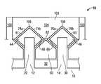
- FIG. 1illustrates, in a cut away perspective view, a portion of a FINFET integrated circuit (IC) 10 .
- the IC 10includes two fins 12 and 14 that are formed from and extend upwardly from a semiconductor substrate 16 (e.g., a bulk semiconductor substrate or silicon-on-insulator (SOI) semiconductor substrate).
- a gate electrode 18overlies the two fins 12 and 14 and is electrically insulated from the fins 12 and 14 by a gate insulator (not illustrated).
- An end 20 of the fin 12is appropriately impurity doped to form a source of a FINFET 22
- an end 24 of the fin 12is appropriately impurity doped to form a drain of the FINFET 22 .
- the ends 26 and 28 of the fin 14form the source and drain, respectively, of another FINFET 30 .
- the illustrated portion of IC 10thus includes two FINFETs 22 and 30 having a common gate electrode 18 .
- the structurewould be a two-fin FINFET having twice the gate width of either FINFET 22 or 30 .
- An oxide layer 32e.g., deposited onto the semiconductor substrate 16 if the semiconductor substrate 16 is a bulk semiconductor substrate, or alternatively, is part of the semiconductor substrate 16 if the semiconductor substrate 16 is an SOI semiconductor substrate) forms electrical isolation between the fins 12 and 14 and between adjacent devices as is needed for the circuit being implemented.
- the channel of the FINFET 22extends along a sidewall 34 of the fin 12 beneath the gate electrode 18 , along a top 36 of the fin 12 , as well as along an opposite sidewall not visible in this perspective view.
- the advantage of the FINFET structureis that although the fin 12 has only the narrow width represented by the arrows 38 , the channel has a width represented by at least twice the height of the fin 12 above the oxide layer 32 . The channel width thus can be much greater than fin width.
- the fins 12 and 14are formed according to known processes. For instance, when using a SOI semiconductor substrate as the semiconductor substrate 16 , portions of the top silicon layer of the semiconductor substrate 16 are etched or otherwise removed leaving the fins 12 and 14 formed from silicon remaining on the underlying oxide layer 32 . As shown, the gate electrode 18 is formed across the fins 12 and 14 . Gate oxide and/or nitride capping layers (not shown) may be deposited over the fins 12 and 14 before the gate electrode 18 is formed. The gate electrode 18 is formed by typical lithographic processing.
- FIGS. 2-9illustrate methods for forming the IC 10 in accordance with various embodiments.
- FIGS. 2-9are cross-sectional views of the source or drain regions 20 , 26 or 24 , 28 of the fins 12 and 14 shown in FIG. 1 during various subsequent stages in the fabrication of the IC 10 .
- the described process steps, procedures, and materialsare to be considered only as exemplary embodiments designed to illustrate to one of ordinary skill in the art methods for practicing the methods contemplated herein; the methods are not limited to these exemplary embodiments.
- the illustrated portion of the IC 10 as shownincludes only two FINFETs 22 and 30 , although those of skill in the art will recognize that an actual IC could include a large number of such transistors.
- Various steps in the manufacture of ICsare well known and so, in the interest of brevity, many conventional steps will only be mentioned briefly herein or will be omitted entirely without providing the well known process details.
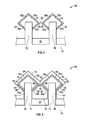
- FIG. 2illustrates, in cross-sectional view, a portion of the IC 10 at an intermediate fabrication stages in accordance with an exemplary embodiment.
- the fins 12 and 14have been formed adjacent to each other extending from the semiconductor substrate 16 and extending above the oxide layer 32 . Further patterning, implanting, and annealing processes are employed to form wells 40 and 42 in the semiconductor substrate 16 below the fins 12 and 14 .
- a selective epitaxial growth processis used to grow a silicon-containing material overlying the upper sections 48 and 50 of the fins 12 and 14 to form epi-portions 44 and 46 , respectively.
- the silicon-containing materialis silicon phosphorus (SiP) for N-type FINFETs or silicon germanium (SiGe) for P-type FINFETs.
- the epi-portions 44 and 46are spaced apart from each other such that the fins 12 and 14 are not merged to define unmerged fins 52 and 54 . As illustrated, the epi-portions 44 and 46 are configured as having “diamond-shaped/cross-sections.” The diamond-shaped/cross-sections of the epi-portions 44 and 46 form due to the slower rate of growth of the silicon-containing material on the (111) surface of the fins 12 and 14 . As such, the epi-portions 44 and 46 have corresponding upper surfaces 56 a, 56 b, 58 a, and 58 b and lower surfaces 60 a, 60 b, 62 a, and 62 b.
- the lower surfaces 60 a, 60 b, 62 a, and 62 bface towards the semiconductor substrate 16 and the upper surfaces 56 a, 56 b, 58 a, and 58 b are positioned beyond the lower surfaces 60 a, 60 b, 62 a, and 62 b facing away from the semiconductor substrate 16 .
- FIG. 3illustrates, in cross-sectional view, a portion of the IC 10 at a further advanced fabrication stage in accordance with an exemplary embodiment.
- silicide layers 61 and 63are formed over the epi-portions 44 and 46 , respectively.
- the silicide layers 61 and 63are formed by depositing a silicide-forming metal overlying the upper surfaces 56 a, 56 b, 58 a, and 58 b and the lower surfaces 60 a, 60 b , 62 a, and 62 b of the epi-portions 44 and 46 , and heating the silicide-forming metal, for example by rapid thermal anneal (RTA), to cause the silicide-forming metal to react with exposed silicon-containing material in the epi-portions 44 and 46 .
- RTArapid thermal anneal
- Examples of silicide-forming metalsinclude, but are not limited to, nickel, cobalt, and alloys thereof.
- the silicide-forming metalcan be deposited, for example by sputtering, to a thickness of from about 3 to about 10 nm, such as about 7 nm. Any unreacted silicide-forming metal can be removed, for example, by wet etching in a H 2 O 2 /H 2 SO 4 or HNO 3 /HCl solution.
- the silicide layers 61 and 63each have a thickness of from about 3 to about 10 nm.
- the silicide formation at both the bottoms and tops of the diamond shaped epi-portions 44 and 46helps maximizes the contact surface area thus reducing contact resistance.
- the silicide layers 61 and 63are spaced apart from each other such that a lateral gap 64 is defined between the silicide layers 61 and 63 proximate the mid-corners 66 and 68 of the diamond-shaped/cross-section of the epi-portions 44 and 46 .
- the lateral gapis from about 3 to about 7 nm.
- the processcontinues as illustrated in FIG. 4 by depositing a dielectric material over the oxide layer 32 and the unmerged fins 52 and 54 including the silicide layers 61 and 63 .
- the dielectric materialis deposited using an atomic layer deposition (ALD) process and comprises silicon nitride (SiN), which may be doped with carbon atoms (C), nitrogen atoms (N), and/or oxygen atoms (O).
- the dielectric materialaccumulates on the upper and lower portions 74 a, 74 b, 76 a, 76 b, 78 a, 78 b, 80 a, and 80 b of the silicide layers 61 and 63 and the surrounding area to form dielectric films 70 and 72 .
- the dielectric films 70 and 72merged together proximate the mid-corners 66 and 68 of the diamond-shaped/cross-sections of the epi-portions 44 and 46 to integrally form a dielectric spacer 82 (indicated by dashed lines). As illustrated, the dielectric spacer 82 spans and closes off the lateral gap 64 .
- the dielectric spacer 82has a lateral dimension of at least about 3 nm, such as about 3 to about 10 nm, for example from about 3 to about 7 nm to close off the lateral gap 64 .
- the upper dielectric film sections 84 and 86 that overlie the upper portions 74 a, 74 b, 76 a, and 76 b of the silicide layers 61 and 63 , respectively,are formed thicker (e.g., with overgrowth) than the lower dielectric film sections 88 and 90 that overlie the lower portions 78 a, 78 b, 80 a, and 80 b of the silicide layers 61 and 63 , respectively.
- the upper dielectric film sections 84 and 86are formed each having a thickness of about 5 to about 15 nm and the lower dielectric film sections 88 and 90 are each formed having a thickness of from about 2 to about 7 nm.
- a void 92is disposed beneath the dielectric spacer 82 between the semiconductor substrate 16 , the lower sections 94 and 96 of the fins 12 and 14 , and the lower dielectric film sections 88 and 90 .
- the void 92enables air trapping beneath the dielectric spacer 82 , and together with the low-k characteristics of the dielectric spacer 82 , enables very low parasitic capacitance.
- FIG. 5illustrates, in cross-sectional view, a portion of the IC 10 at a further advanced fabrication stage in accordance with an exemplary embodiment.
- the upper dielectric film sections 84 and 86are removed by etching the dielectric material to expose the upper portions 74 a, 74 b, 76 a, and 76 b of the silicide layers 61 and 63 while leaving the dielectric spacer 82 intact.
- the dielectric materialis etched using a dry etching process, such as a plasma etching process, for example reactive ion etching (RIE).
- RIEreactive ion etching
- the dielectric materialis etched using a wet etching process, such as a hot phosphoric acid etching process at a temperature of about 160 to about 170° C.
- a wet etching processsuch as a hot phosphoric acid etching process at a temperature of about 160 to about 170° C.
- the methodcontinues as illustrated in FIGS. 6 and 7 by forming a nitride etch layer 98 overlying the dielectric spacer 82 and the upper portions 74 a, 74 b, 76 a, and 76 b of the silicide layers 61 and 63 .
- An ILD layer 100 of insulating materiale.g., silicon oxide
- the ILD layer 100is deposited by a low pressure chemical vapor deposition (LPCVD) process.
- LPCVDlow pressure chemical vapor deposition
- CMPchemical mechanical planarization
- FIGS. 8-9illustrate, in cross sectional views, the IC 10 at further advanced fabrication stages in accordance with an exemplary embodiment.
- the methodcontinues by etching through the ILD layer 100 and the nitride etch stop layer 98 to form a contact opening 102 .
- the contact opening 102exposes the dielectric spacer 82 and the upper portions 74 a, 74 b, 76 a, and 76 b of the silicide layers 61 and 63 .
- a contact-forming material 103(e.g., conductive metal) is deposited into the contact opening 102 to form a contact plug 104 that overlies the dielectric spacer 82 and the upper portions 74 a , 74 b, 76 a, and 76 b of the silicide layers 61 and 63 .
- the contact-forming material 103is tungsten (W).
- the void 92which has been protectively covered by the dielectric spacer 82 during deposition of the contact forming material 103 , is substantially free of the contact-forming material 103 , thereby reducing parasitic capacitance compared to conventional ICs with unmerged fins.
- the contact plug 104contacts the silicide layers 61 and 63 horizontally up from about the mid-corners 66 and 68 of the epi-portions 44 and 46 to the uppermost portions 106 and 108 of the silicide layers 61 and 63 .
- the FINFETs 22 and 30have more contact area and thus lower contact resistance than conventional FINFET devices with unmerged fins that have small contacts formed only at the very tops of the fins. Any excess contact-forming material that is disposed above the ILD layer 100 is then removed using CMP.
- unmerged finsare formed in which a first fin has a first epi-portion and a second fin has a second epi-portion.
- a first silicide layeris formed overlying a first epi-portion and a second silicide layer is formed overlying the second epi-portion.
- the first and second silicide layersare spaced apart from each other to define a lateral gap.
- a dielectric materialis deposited overlying the first and second silicide layers to form a dielectric spacer that spans the lateral gap.
- the dielectric material that overlies portions of the first and second silicide layers laterally above the dielectric spaceris removed while leaving the dielectric spacer intact.
- a contact-forming materialis deposited overlying the dielectric spacer and the portions of the first and second silicide layers.
Landscapes
- Engineering & Computer Science (AREA)
- Physics & Mathematics (AREA)
- Condensed Matter Physics & Semiconductors (AREA)
- General Physics & Mathematics (AREA)
- Manufacturing & Machinery (AREA)
- Computer Hardware Design (AREA)
- Microelectronics & Electronic Packaging (AREA)
- Power Engineering (AREA)
- Thin Film Transistor (AREA)
- Insulated Gate Type Field-Effect Transistor (AREA)
Abstract
Description
Claims (14)
Priority Applications (4)
| Application Number | Priority Date | Filing Date | Title |
|---|---|---|---|
| US13/759,156US8921191B2 (en) | 2013-02-05 | 2013-02-05 | Integrated circuits including FINFET devices with lower contact resistance and reduced parasitic capacitance and methods for fabricating the same |
| TW102130763ATWI525745B (en) | 2013-02-05 | 2013-08-28 | Integrated circuit including fin field effect transistor device with lower contact resistance and reduced parasitic capacitance and manufacturing method thereof |
| CN201410044017.7ACN103972236B (en) | 2013-02-05 | 2014-01-30 | Comprise integrated circuit and the manufacture method thereof of fin field effect electric crystal device |
| US14/551,606US9425319B2 (en) | 2013-02-05 | 2014-11-24 | Integrated circuits including FINFET devices with lower contact resistance and reduced parasitic capacitance and methods for fabricating the same |
Applications Claiming Priority (1)
| Application Number | Priority Date | Filing Date | Title |
|---|---|---|---|
| US13/759,156US8921191B2 (en) | 2013-02-05 | 2013-02-05 | Integrated circuits including FINFET devices with lower contact resistance and reduced parasitic capacitance and methods for fabricating the same |
Related Child Applications (1)
| Application Number | Title | Priority Date | Filing Date |
|---|---|---|---|
| US14/551,606DivisionUS9425319B2 (en) | 2013-02-05 | 2014-11-24 | Integrated circuits including FINFET devices with lower contact resistance and reduced parasitic capacitance and methods for fabricating the same |
Publications (2)
| Publication Number | Publication Date |
|---|---|
| US20140217517A1 US20140217517A1 (en) | 2014-08-07 |
| US8921191B2true US8921191B2 (en) | 2014-12-30 |
Family
ID=51241551
Family Applications (2)
| Application Number | Title | Priority Date | Filing Date |
|---|---|---|---|
| US13/759,156Active2033-03-07US8921191B2 (en) | 2013-02-05 | 2013-02-05 | Integrated circuits including FINFET devices with lower contact resistance and reduced parasitic capacitance and methods for fabricating the same |
| US14/551,606Expired - Fee RelatedUS9425319B2 (en) | 2013-02-05 | 2014-11-24 | Integrated circuits including FINFET devices with lower contact resistance and reduced parasitic capacitance and methods for fabricating the same |
Family Applications After (1)
| Application Number | Title | Priority Date | Filing Date |
|---|---|---|---|
| US14/551,606Expired - Fee RelatedUS9425319B2 (en) | 2013-02-05 | 2014-11-24 | Integrated circuits including FINFET devices with lower contact resistance and reduced parasitic capacitance and methods for fabricating the same |
Country Status (3)
| Country | Link |
|---|---|
| US (2) | US8921191B2 (en) |
| CN (1) | CN103972236B (en) |
| TW (1) | TWI525745B (en) |
Cited By (18)
| Publication number | Priority date | Publication date | Assignee | Title |
|---|---|---|---|---|
| US20150102422A1 (en)* | 2013-02-05 | 2015-04-16 | GlobalFoundries, Inc. | Integrated circuits including finfet devices with lower contact resistance and reduced parasitic capacitance and methods for fabricating the same |
| US20160300911A1 (en)* | 2013-03-12 | 2016-10-13 | Taiwan Semiconductor Manufacturing Company, Ltd. | Heterostructures for Semiconductor Devices and Methods of Forming the Same |
| US20160359044A1 (en)* | 2015-06-04 | 2016-12-08 | International Business Machines Corporation | FORMATION OF DISLOCATION-FREE SiGe FINFET USING POROUS SILICON |
| US9564358B1 (en) | 2015-09-09 | 2017-02-07 | International Business Machines Corporation | Forming reliable contacts on tight semiconductor pitch |
| US9680020B2 (en) | 2015-07-09 | 2017-06-13 | Globalfoundries Inc. | Increased contact area for FinFETs |
| US9812332B2 (en) | 2016-01-05 | 2017-11-07 | Samsung Electronics Co., Ltd. | Etching methods and methods of manufacturing semiconductor devices using the same |
| US9837407B1 (en) | 2016-09-06 | 2017-12-05 | International Business Machines Corporation | Semiconductor device with increased source/drain area |
| US9941277B2 (en) | 2015-03-25 | 2018-04-10 | Samsung Electronics Co., Ltd. | Semiconductor devices including increased area contacts |
| US9954107B2 (en)* | 2015-05-05 | 2018-04-24 | International Business Machines Corporation | Strained FinFET source drain isolation |
| US10026809B1 (en) | 2016-12-22 | 2018-07-17 | Samsung Electronics Co., Ltd. | Semiconductor device |
| US10032884B2 (en) | 2015-10-22 | 2018-07-24 | International Business Machines Corporation | Unmerged epitaxial process for FinFET devices with aggressive fin pitch scaling |
| US10141307B2 (en) | 2016-03-03 | 2018-11-27 | Taiwan Semiconductor Manufacturing Company, Ltd. | Semiconductor device and manufacturing method thereof |
| US10998241B2 (en) | 2018-09-19 | 2021-05-04 | Taiwan Semiconductor Manufacturing Co., Ltd. | Selective dual silicide formation using a maskless fabrication process flow |
| US11133401B2 (en)* | 2017-08-30 | 2021-09-28 | Taiwan Semiconductor Manufacturing Co., Ltd. | Fin structures having varied fin heights for semiconductor device |
| TWI745741B (en)* | 2018-09-19 | 2021-11-11 | 台灣積體電路製造股份有限公司 | Semiconductor device and fabricating the same |
| US11211473B2 (en)* | 2016-11-30 | 2021-12-28 | Taiwan Semiconductor Manufacturing Co., Ltd. | Epitaxial fin structures having an epitaxial buffer region and an epitaxial capping region |
| US11244864B2 (en) | 2020-04-21 | 2022-02-08 | International Business Machines Corporation | Reducing parasitic capacitance within semiconductor devices |
| US12419092B2 (en) | 2017-08-30 | 2025-09-16 | Taiwan Semiconductor Manufacturing Company, Ltd. | Fin structures having varied fin heights for semiconductor device |
Families Citing this family (79)
| Publication number | Priority date | Publication date | Assignee | Title |
|---|---|---|---|---|
| US9397098B2 (en)* | 2012-03-08 | 2016-07-19 | Taiwan Semiconductor Manufacturing Company, Ltd. | FinFET-based ESD devices and methods for forming the same |
| US8779517B2 (en) | 2012-03-08 | 2014-07-15 | Taiwan Semiconductor Manufacturing Company, Ltd. | FinFET-based ESD devices and methods for forming the same |
| US9147682B2 (en)* | 2013-01-14 | 2015-09-29 | Taiwan Semiconductor Manufacturing Company, Ltd. | Fin spacer protected source and drain regions in FinFETs |
| US9752251B2 (en)* | 2013-04-15 | 2017-09-05 | International Business Machines Corporation | Self-limiting selective epitaxy process for preventing merger of semiconductor fins |
| US9054218B2 (en) | 2013-08-07 | 2015-06-09 | International Business Machines Corporation | Method of manufacturing a FinFET device using a sacrificial epitaxy region for improved fin merge and FinFET device formed by same |
| US9214556B2 (en) | 2013-08-09 | 2015-12-15 | Taiwan Semiconductor Manufacturing Company, Ltd. | Self-aligned dual-metal silicide and germanide formation |
| US20150087144A1 (en)* | 2013-09-26 | 2015-03-26 | Taiwan Semiconductor Manufacturing Company Ltd. | Apparatus and method of manufacturing metal gate semiconductor device |
| US9472652B2 (en) | 2013-12-20 | 2016-10-18 | Taiwan Semiconductor Manufacturing Company, Ltd. | Fin structure of semiconductor device |
| US9425310B2 (en)* | 2014-03-04 | 2016-08-23 | Taiwan Semiconductor Manufacturing Co., Ltd. | Methods for forming wrap around contact |
| US9406804B2 (en)* | 2014-04-11 | 2016-08-02 | Taiwan Semiconductor Manufacturing Company, Ltd. | FinFETs with contact-all-around |
| US9443769B2 (en) | 2014-04-21 | 2016-09-13 | Taiwan Semiconductor Manufacturing Company, Ltd. | Wrap-around contact |
| US9373550B2 (en) | 2014-04-23 | 2016-06-21 | International Business Machines Corporation | Selectively degrading current resistance of field effect transistor devices |
| US9349649B2 (en) | 2014-06-26 | 2016-05-24 | Globalfoundries Inc. | Low resistance and defect free epitaxial semiconductor material for providing merged FinFETs |
| US9966471B2 (en)* | 2014-06-27 | 2018-05-08 | Taiwan Semiconductor Manufacturing Company, Ltd. | Stacked Gate-All-Around FinFET and method forming the same |
| US9543438B2 (en) | 2014-10-15 | 2017-01-10 | Taiwan Semiconductor Manufacturing Company, Ltd. | Contact resistance reduction technique |
| US10164108B2 (en)* | 2014-10-17 | 2018-12-25 | Taiwan Semiconductor Manufacturing Co., Ltd. | Fin field effect transistor (FinFET) device and method for forming the same |
| US9431303B2 (en)* | 2014-10-17 | 2016-08-30 | Globalfoundries Inc. | Contact liners for integrated circuits and fabrication methods thereof |
| US9472470B2 (en) | 2014-12-09 | 2016-10-18 | GlobalFoundries, Inc. | Methods of forming FinFET with wide unmerged source drain EPI |
| KR20160072476A (en)* | 2014-12-15 | 2016-06-23 | 삼성전자주식회사 | Semiconductor device and method of fabricating the same |
| CN105845725B (en)* | 2015-01-12 | 2019-01-22 | 中芯国际集成电路制造(上海)有限公司 | A semiconductor device and its manufacturing method and electronic device |
| KR102379267B1 (en) | 2015-04-01 | 2022-03-28 | 삼성전자주식회사 | Semiconductor Devices Having a Spacer on an Isolation Region |
| US9443853B1 (en) | 2015-04-07 | 2016-09-13 | International Business Machines Corporation | Minimizing shorting between FinFET epitaxial regions |
| KR102326316B1 (en)* | 2015-04-10 | 2021-11-16 | 삼성전자주식회사 | Semiconductor dievices and methods of manufacturing the same |
| KR102432268B1 (en)* | 2015-04-14 | 2022-08-12 | 삼성전자주식회사 | A semiconductor device and method of manufacturing the semiconductor device |
| KR102310076B1 (en) | 2015-04-23 | 2021-10-08 | 삼성전자주식회사 | Semiconductor devices having a source/drain ofasymmetrical shape |
| KR102400375B1 (en) | 2015-04-30 | 2022-05-20 | 삼성전자주식회사 | Semiconductor devices and methods of manufacturing the same |
| US9741829B2 (en)* | 2015-05-15 | 2017-08-22 | Taiwan Semiconductor Manufacturing Co., Ltd. | Semiconductor device and manufacturing method thereof |
| US10483262B2 (en) | 2015-05-15 | 2019-11-19 | Taiwan Semiconductor Manufacturing Co., Ltd. | Dual nitride stressor for semiconductor device and method of manufacturing |
| KR20160143942A (en) | 2015-06-04 | 2016-12-15 | 삼성전자주식회사 | Method of manufacturing semiconductor device |
| KR102310081B1 (en) | 2015-06-08 | 2021-10-12 | 삼성전자주식회사 | Methods of manufacturing semiconductor devices |
| KR102258109B1 (en)* | 2015-06-08 | 2021-05-28 | 삼성전자주식회사 | Semiconductor device blocking a leakage current and method for fabricating the same |
| US9722043B2 (en) | 2015-06-15 | 2017-08-01 | International Business Machines Corporation | Self-aligned trench silicide process for preventing gate contact to silicide shorts |
| US9627278B2 (en) | 2015-06-16 | 2017-04-18 | International Business Machines Corporation | Method of source/drain height control in dual epi finFET formation |
| US9455331B1 (en) | 2015-07-10 | 2016-09-27 | International Business Machines Corporation | Method and structure of forming controllable unmerged epitaxial material |
| KR102422430B1 (en) | 2015-07-16 | 2022-07-18 | 삼성전자주식회사 | Semiconductor device and fabricating method thereof |
| US10158003B2 (en) | 2015-08-12 | 2018-12-18 | International Business Machines Corporation | Epitaxial and silicide layer formation at top and bottom surfaces of semiconductor fins |
| US10366988B2 (en) | 2015-08-14 | 2019-07-30 | International Business Machines Corporation | Selective contact etch for unmerged epitaxial source/drain regions |
| US9620644B2 (en)* | 2015-09-02 | 2017-04-11 | International Business Machines Corporation | Composite spacer enabling uniform doping in recessed fin devices |
| US9472620B1 (en)* | 2015-09-04 | 2016-10-18 | Taiwan Semiconductor Manufacturing Co., Ltd. | Semiconductor device including fin structures and manufacturing method thereof |
| US10103249B2 (en) | 2015-09-10 | 2018-10-16 | Taiwan Semiconductor Manufacturing Co., Ltd. | FinFET device and method for fabricating the same |
| US9905641B2 (en)* | 2015-09-15 | 2018-02-27 | Taiwan Semiconductor Manufacturing Company, Ltd. | Semiconductor device and manufacturing method thereof |
| DE102016102679B4 (en) | 2015-09-15 | 2024-09-12 | Taiwan Semiconductor Manufacturing Co., Ltd. | FETS AND METHODS OF FORMING FETS |
| US9831116B2 (en)* | 2015-09-15 | 2017-11-28 | Taiwan Semiconductor Manufacturing Company, Ltd. | FETS and methods of forming FETs |
| CN108028280B (en)* | 2015-09-25 | 2023-04-04 | 英特尔公司 | Method for manufacturing wound source/drain electrode of contact part of back side metal |
| US10177143B2 (en) | 2015-10-28 | 2019-01-08 | Taiwan Semiconductor Manufacturing Company Limited | FinFET device and method for fabricating the same |
| US9601586B1 (en) | 2015-11-02 | 2017-03-21 | Samsung Electronics Co., Ltd. | Methods of forming semiconductor devices, including forming a metal layer on source/drain regions |
| US10497701B2 (en)* | 2015-12-16 | 2019-12-03 | Taiwan Semiconductor Manufacturing Co., Ltd. | Semiconductor device and manufacturing method thereof |
| TWI707403B (en)* | 2016-01-06 | 2020-10-11 | 聯華電子股份有限公司 | Semiconductor device and method for fabricating the same |
| US10249502B2 (en) | 2016-01-22 | 2019-04-02 | International Business Machines Corporation | Low resistance source drain contact formation with trench metastable alloys and laser annealing |
| US20170250268A1 (en)* | 2016-02-25 | 2017-08-31 | Taiwan Semiconductor Manufacturing Co., Ltd. | Fin field effect transistor and method for fabricating the same |
| US9865504B2 (en)* | 2016-03-04 | 2018-01-09 | Taiwan Semiconductor Manufacturing Company, Ltd. | Semiconductor device and manufacturing method thereof |
| US10205025B2 (en)* | 2016-03-11 | 2019-02-12 | Samsung Electronics Co., Ltd. | Methods to achieve strained channel finFET devices |
| CN107369621B (en)* | 2016-05-13 | 2020-03-10 | 中芯国际集成电路制造(上海)有限公司 | Fin field effect transistor and forming method thereof |
| US10157918B2 (en) | 2016-08-03 | 2018-12-18 | Taiwan Semiconductor Manufacturing Company, Ltd. | Semiconductor device and method |
| US9805989B1 (en) | 2016-09-22 | 2017-10-31 | International Business Machines Corporation | Sacrificial cap for forming semiconductor contact |
| US10535652B2 (en)* | 2016-10-27 | 2020-01-14 | International Business Machines Corporation | Fabrication of vertical fin field effect transistors having top air spacers and a self-aligned top junction |
| US10872889B2 (en)* | 2016-11-17 | 2020-12-22 | Taiwan Semiconductor Manufacturing Co., Ltd. | Semiconductor component and fabricating method thereof |
| TWI778048B (en)* | 2017-04-20 | 2022-09-21 | 美商微材料有限責任公司 | Methods of forming semiconductor structures |
| US10164065B1 (en)* | 2017-05-31 | 2018-12-25 | Taiwan Semiconductor Manufacturing Co., Ltd. | Film deposition for 3D semiconductor structure |
| US10510875B2 (en)* | 2017-07-31 | 2019-12-17 | Taiwan Semiconductor Manufacturing Co., Ltd. | Source and drain structure with reduced contact resistance and enhanced mobility |
| KR102432467B1 (en)* | 2017-08-30 | 2022-08-12 | 삼성전자주식회사 | Semiconductor device and method for fabricating the same |
| US10763104B2 (en) | 2017-09-28 | 2020-09-01 | Taiwan Semiconductor Manufacturing Co., Ltd. | Method of forming differential etch stop layer using directional plasma to activate surface on device structure |
| US10347744B1 (en) | 2018-01-09 | 2019-07-09 | International Business Machines Corporation | Method and structure of forming FinFET contact |
| CN110416297B (en)* | 2018-04-27 | 2023-07-04 | 中芯国际集成电路制造(上海)有限公司 | N-type fin field effect transistor and forming method thereof |
| US10373877B1 (en) | 2018-05-22 | 2019-08-06 | Globalfoundries Inc. | Methods of forming source/drain contact structures on integrated circuit products |
| US10854716B2 (en) | 2018-07-30 | 2020-12-01 | Taiwan Semiconductor Manufacturing Co., Ltd. | Semiconductor device with source/drain contact formed using bottom-up deposition |
| US10804368B2 (en) | 2018-07-30 | 2020-10-13 | International Business Machines Corporation | Semiconductor device having two-part spacer |
| US10943818B2 (en)* | 2018-10-31 | 2021-03-09 | Taiwan Semiconductor Manufacturing Company, Ltd. | Semiconductor device and method |
| US11121238B2 (en)* | 2018-11-29 | 2021-09-14 | Taiwan Semiconductor Manufacturing Co., Ltd. | Semiconductor device and manufacturing method thereof |
| US11107752B2 (en)* | 2020-01-03 | 2021-08-31 | International Business Machines Corporation | Half buried nFET/pFET epitaxy source/drain strap |
| US11164774B2 (en)* | 2020-01-16 | 2021-11-02 | International Business Machines Corporation | Interconnects with spacer structure for forming air-gaps |
| US11450572B2 (en)* | 2020-05-22 | 2022-09-20 | Taiwan Semiconductor Manufacturing Co., Ltd. | Semiconductor device and method |
| US11888064B2 (en) | 2020-06-01 | 2024-01-30 | Taiwan Semiconductor Manufacturing Co., Ltd. | Semiconductor device and method |
| US11515165B2 (en) | 2020-06-11 | 2022-11-29 | Taiwan Semiconductor Manufacturing Co., Ltd. | Semiconductor device and method |
| US11502200B2 (en)* | 2020-06-19 | 2022-11-15 | Globalfoundries U.S. Inc. | Transistor device having sidewall spacers contacting lower surfaces of an epitaxial semiconductor material |
| US11605673B2 (en) | 2020-12-09 | 2023-03-14 | International Business Machines Corporation | Dual resistive random-access memory with two transistors |
| CN112582478B (en)* | 2020-12-30 | 2022-08-19 | 上海集成电路装备材料产业创新中心有限公司 | Fin type field effect transistor and preparation method thereof |
| US11735483B2 (en)* | 2021-02-26 | 2023-08-22 | Taiwan Semiconductor Manufacturing Company, Ltd. | Method for forming epitaxial source/drain features using a self-aligned mask and semiconductor devices fabricated thereof |
| KR20220135684A (en)* | 2021-03-31 | 2022-10-07 | 삼성전자주식회사 | Temperature sensig device and system on chip |
Citations (10)
| Publication number | Priority date | Publication date | Assignee | Title |
|---|---|---|---|---|
| US20090026505A1 (en)* | 2007-07-27 | 2009-01-29 | Kabushiki Kaisha Toshiba | Semiconductor device and method of fabricating the same |
| US20110193175A1 (en)* | 2010-02-09 | 2011-08-11 | Taiwan Semiconductor Manufacturing Co., Ltd. | Lower parasitic capacitance finfet |
| US20110210404A1 (en)* | 2010-02-26 | 2011-09-01 | Taiwan Seminconductor Manufacturing Company, Ltd. | Epitaxy Profile Engineering for FinFETs |
| US20110298058A1 (en)* | 2010-06-04 | 2011-12-08 | Toshiba America Electronic Components, Inc. | Faceted epi shape and half-wrap around silicide in s/d merged finfet |
| US20130153960A1 (en)* | 2011-12-16 | 2013-06-20 | Taiwan Semiconductor Manufacturing Company, Ltd. | Anti-Fuses on Semiconductor Fins |
| US20130187228A1 (en)* | 2012-01-19 | 2013-07-25 | Globalfoundries Inc. | FinFET Semiconductor Devices with Improved Source/Drain Resistance and Methods of Making Same |
| US20130193446A1 (en)* | 2012-01-31 | 2013-08-01 | Taiwan Semiconductor Manufacturing Company, Ltd. | Finfet and method of fabricating the same |
| US20140183605A1 (en)* | 2012-12-28 | 2014-07-03 | International Business Machines Corporation | Semiconductor device and method of manufacturing the semiconductor device |
| US20140203370A1 (en)* | 2013-01-24 | 2014-07-24 | Shigenobu Maeda | Semiconductor Device and Fabricating Method Thereof |
| US20140217517A1 (en)* | 2013-02-05 | 2014-08-07 | International Business Machines Corporation | Integrated circuits including finfet devices with lower contact resistance and reduced parasitic capacitance and methods for fabricating the same |
Family Cites Families (27)
| Publication number | Priority date | Publication date | Assignee | Title |
|---|---|---|---|---|
| US7425500B2 (en)* | 2006-03-31 | 2008-09-16 | Intel Corporation | Uniform silicide metal on epitaxially grown source and drain regions of three-dimensional transistors |
| US7560344B2 (en)* | 2006-11-15 | 2009-07-14 | Samsung Electronics Co., Ltd. | Semiconductor device having a pair of fins and method of manufacturing the same |
| KR101225641B1 (en)* | 2006-12-27 | 2013-01-24 | 삼성전자주식회사 | Semiconductor device and method of fabricating the same |
| US8030108B1 (en)* | 2008-06-30 | 2011-10-04 | Stc.Unm | Epitaxial growth of in-plane nanowires and nanowire devices |
| US7910453B2 (en)* | 2008-07-14 | 2011-03-22 | Taiwan Semiconductor Manufacturing Company, Ltd. | Storage nitride encapsulation for non-planar sonos NAND flash charge retention |
| US8116121B2 (en)* | 2009-03-06 | 2012-02-14 | Kabushiki Kaisha Toshiba | Semiconductor device and manufacturing methods with using non-planar type of transistors |
| US8426923B2 (en)* | 2009-12-02 | 2013-04-23 | Taiwan Semiconductor Manufacturing Company, Ltd. | Multiple-gate semiconductor device and method |
| US8258572B2 (en)* | 2009-12-07 | 2012-09-04 | Taiwan Semiconductor Manufacturing Company, Ltd. | SRAM structure with FinFETs having multiple fins |
| US8937353B2 (en)* | 2010-03-01 | 2015-01-20 | Taiwan Semiconductor Manufacturing Co., Ltd. | Dual epitaxial process for a finFET device |
| JP2012018968A (en) | 2010-07-06 | 2012-01-26 | Elpida Memory Inc | Semiconductor device manufacturing method |
| JP2013115272A (en)* | 2011-11-29 | 2013-06-10 | Toshiba Corp | Semiconductor device and method of manufacturing the same |
| US8377779B1 (en)* | 2012-01-03 | 2013-02-19 | Taiwan Semiconductor Manufacturing Company, Ltd. | Methods of manufacturing semiconductor devices and transistors |
| US20130221414A1 (en)* | 2012-02-27 | 2013-08-29 | Chao Zhao | Semiconductor FET and Method for Manufacturing the Same |
| TWI449802B (en)* | 2012-06-06 | 2014-08-21 | Univ Nat Chiao Tung | Carbon-doped silicon nitride thin film and manufacturing method and device thereof |
| US10535735B2 (en)* | 2012-06-29 | 2020-01-14 | Intel Corporation | Contact resistance reduced P-MOS transistors employing Ge-rich contact layer |
| US8846477B2 (en)* | 2012-09-27 | 2014-09-30 | Globalfoundries Inc. | Methods of forming 3-D semiconductor devices using a replacement gate technique and a novel 3-D device |
| US8946029B2 (en)* | 2012-11-12 | 2015-02-03 | GlobalFoundries, Inc. | Methods of manufacturing integrated circuits having FinFET structures with epitaxially formed source/drain regions |
| US9142633B2 (en)* | 2012-12-13 | 2015-09-22 | GlobalFoundries, Inc. | Integrated circuits and methods for fabricating integrated circuits with silicide contacts on non-planar structures |
| US8956942B2 (en)* | 2012-12-21 | 2015-02-17 | Stmicroelectronics, Inc. | Method of forming a fully substrate-isolated FinFET transistor |
| KR102068980B1 (en)* | 2013-08-01 | 2020-01-22 | 삼성전자 주식회사 | Semiconductor device and method for fabricating the same |
| US9214556B2 (en)* | 2013-08-09 | 2015-12-15 | Taiwan Semiconductor Manufacturing Company, Ltd. | Self-aligned dual-metal silicide and germanide formation |
| US8999779B2 (en)* | 2013-09-06 | 2015-04-07 | International Business Machines Corporation | Locally raised epitaxy for improved contact by local silicon capping during trench silicide processings |
| US9202918B2 (en)* | 2013-09-18 | 2015-12-01 | Globalfoundries Inc. | Methods of forming stressed layers on FinFET semiconductor devices and the resulting devices |
| US9324790B2 (en)* | 2013-11-19 | 2016-04-26 | International Business Machines Corporation | Self-aligned dual-height isolation for bulk FinFET |
| US9391077B2 (en)* | 2014-02-10 | 2016-07-12 | International Business Machines Corporation | SiGe and Si FinFET structures and methods for making the same |
| US9871121B2 (en)* | 2014-03-10 | 2018-01-16 | Qualcomm Incorporated | Semiconductor device having a gap defined therein |
| US9443769B2 (en)* | 2014-04-21 | 2016-09-13 | Taiwan Semiconductor Manufacturing Company, Ltd. | Wrap-around contact |
- 2013
- 2013-02-05USUS13/759,156patent/US8921191B2/enactiveActive
- 2013-08-28TWTW102130763Apatent/TWI525745B/enactive
- 2014
- 2014-01-30CNCN201410044017.7Apatent/CN103972236B/ennot_activeExpired - Fee Related
- 2014-11-24USUS14/551,606patent/US9425319B2/ennot_activeExpired - Fee Related
Patent Citations (16)
| Publication number | Priority date | Publication date | Assignee | Title |
|---|---|---|---|---|
| US20090026505A1 (en)* | 2007-07-27 | 2009-01-29 | Kabushiki Kaisha Toshiba | Semiconductor device and method of fabricating the same |
| US8697539B2 (en)* | 2010-02-09 | 2014-04-15 | Taiwan Semiconductor Manufacturing Co., Ltd. | Method of making lower parasitic capacitance FinFET |
| US20110193175A1 (en)* | 2010-02-09 | 2011-08-11 | Taiwan Semiconductor Manufacturing Co., Ltd. | Lower parasitic capacitance finfet |
| US20130109152A1 (en)* | 2010-02-09 | 2013-05-02 | Taiwan Semiconductor Manufacturing Co., Ltd. | Method of making lower parasitic capacitance finfet |
| US20110210404A1 (en)* | 2010-02-26 | 2011-09-01 | Taiwan Seminconductor Manufacturing Company, Ltd. | Epitaxy Profile Engineering for FinFETs |
| US20110298058A1 (en)* | 2010-06-04 | 2011-12-08 | Toshiba America Electronic Components, Inc. | Faceted epi shape and half-wrap around silicide in s/d merged finfet |
| US20140179070A1 (en)* | 2011-12-16 | 2014-06-26 | Taiwan Semiconductor Manufacturing Company, Ltd. | Anti-Fuses on Semiconductor Fins |
| US8742457B2 (en)* | 2011-12-16 | 2014-06-03 | Taiwan Semiconductor Manufacturing Company, Ltd. | Anti-fuses on semiconductor fins |
| US20130153960A1 (en)* | 2011-12-16 | 2013-06-20 | Taiwan Semiconductor Manufacturing Company, Ltd. | Anti-Fuses on Semiconductor Fins |
| US20130187228A1 (en)* | 2012-01-19 | 2013-07-25 | Globalfoundries Inc. | FinFET Semiconductor Devices with Improved Source/Drain Resistance and Methods of Making Same |
| US20130193446A1 (en)* | 2012-01-31 | 2013-08-01 | Taiwan Semiconductor Manufacturing Company, Ltd. | Finfet and method of fabricating the same |
| US8659032B2 (en)* | 2012-01-31 | 2014-02-25 | Taiwan Semiconductor Manufacturing Company, Ltd. | FinFET and method of fabricating the same |
| US20140134831A1 (en)* | 2012-01-31 | 2014-05-15 | Taiwan Semiconductor Manufacturing Company, Ltd. | Finfet and method of fabricating the same |
| US20140183605A1 (en)* | 2012-12-28 | 2014-07-03 | International Business Machines Corporation | Semiconductor device and method of manufacturing the semiconductor device |
| US20140203370A1 (en)* | 2013-01-24 | 2014-07-24 | Shigenobu Maeda | Semiconductor Device and Fabricating Method Thereof |
| US20140217517A1 (en)* | 2013-02-05 | 2014-08-07 | International Business Machines Corporation | Integrated circuits including finfet devices with lower contact resistance and reduced parasitic capacitance and methods for fabricating the same |
Cited By (29)
| Publication number | Priority date | Publication date | Assignee | Title |
|---|---|---|---|---|
| US9425319B2 (en)* | 2013-02-05 | 2016-08-23 | GlobalFoundries, Inc. | Integrated circuits including FINFET devices with lower contact resistance and reduced parasitic capacitance and methods for fabricating the same |
| US20150102422A1 (en)* | 2013-02-05 | 2015-04-16 | GlobalFoundries, Inc. | Integrated circuits including finfet devices with lower contact resistance and reduced parasitic capacitance and methods for fabricating the same |
| US20160300911A1 (en)* | 2013-03-12 | 2016-10-13 | Taiwan Semiconductor Manufacturing Company, Ltd. | Heterostructures for Semiconductor Devices and Methods of Forming the Same |
| US10164024B2 (en)* | 2013-03-12 | 2018-12-25 | Taiwan Semiconductor Manufacturing Company, Ltd. | Heterostructures for semiconductor devices and methods of forming the same |
| US9941277B2 (en) | 2015-03-25 | 2018-04-10 | Samsung Electronics Co., Ltd. | Semiconductor devices including increased area contacts |
| US9954107B2 (en)* | 2015-05-05 | 2018-04-24 | International Business Machines Corporation | Strained FinFET source drain isolation |
| US10586867B2 (en) | 2015-05-05 | 2020-03-10 | International Business Machines Corporation | Strained FinFET source drain isloation |
| US20160359044A1 (en)* | 2015-06-04 | 2016-12-08 | International Business Machines Corporation | FORMATION OF DISLOCATION-FREE SiGe FINFET USING POROUS SILICON |
| US10833175B2 (en)* | 2015-06-04 | 2020-11-10 | International Business Machines Corporation | Formation of dislocation-free SiGe finFET using porous silicon |
| US9680020B2 (en) | 2015-07-09 | 2017-06-13 | Globalfoundries Inc. | Increased contact area for FinFETs |
| US9899525B2 (en) | 2015-07-09 | 2018-02-20 | Globalfoundries Inc. | Increased contact area for finFETs |
| US9564358B1 (en) | 2015-09-09 | 2017-02-07 | International Business Machines Corporation | Forming reliable contacts on tight semiconductor pitch |
| US9634004B2 (en) | 2015-09-09 | 2017-04-25 | International Business Machines Corporation | Forming reliable contacts on tight semiconductor pitch |
| US10734499B2 (en) | 2015-10-22 | 2020-08-04 | International Business Machines Corporation | Unmerged epitaxial process for FinFET devices with aggressive fin pitch scaling |
| US10032884B2 (en) | 2015-10-22 | 2018-07-24 | International Business Machines Corporation | Unmerged epitaxial process for FinFET devices with aggressive fin pitch scaling |
| US10388754B2 (en) | 2015-10-22 | 2019-08-20 | International Business Machines Corporation | Unmerged epitaxial process for FinFET devices with aggressive fin pitch scaling |
| US9812332B2 (en) | 2016-01-05 | 2017-11-07 | Samsung Electronics Co., Ltd. | Etching methods and methods of manufacturing semiconductor devices using the same |
| US10141307B2 (en) | 2016-03-03 | 2018-11-27 | Taiwan Semiconductor Manufacturing Company, Ltd. | Semiconductor device and manufacturing method thereof |
| US9837407B1 (en) | 2016-09-06 | 2017-12-05 | International Business Machines Corporation | Semiconductor device with increased source/drain area |
| US11211473B2 (en)* | 2016-11-30 | 2021-12-28 | Taiwan Semiconductor Manufacturing Co., Ltd. | Epitaxial fin structures having an epitaxial buffer region and an epitaxial capping region |
| US11888046B2 (en) | 2016-11-30 | 2024-01-30 | Taiwan Semiconductor Manufacturing Co., Ltd. | Epitaxial fin structures of finFET having an epitaxial buffer region and an epitaxial capping region |
| US10026809B1 (en) | 2016-12-22 | 2018-07-17 | Samsung Electronics Co., Ltd. | Semiconductor device |
| US11133401B2 (en)* | 2017-08-30 | 2021-09-28 | Taiwan Semiconductor Manufacturing Co., Ltd. | Fin structures having varied fin heights for semiconductor device |
| US12419092B2 (en) | 2017-08-30 | 2025-09-16 | Taiwan Semiconductor Manufacturing Company, Ltd. | Fin structures having varied fin heights for semiconductor device |
| US10998241B2 (en) | 2018-09-19 | 2021-05-04 | Taiwan Semiconductor Manufacturing Co., Ltd. | Selective dual silicide formation using a maskless fabrication process flow |
| TWI745741B (en)* | 2018-09-19 | 2021-11-11 | 台灣積體電路製造股份有限公司 | Semiconductor device and fabricating the same |
| US11749682B2 (en) | 2018-09-19 | 2023-09-05 | Taiwan Semiconductor Manufacturing Co., Ltd. | Selective dual silicide formation using a maskless fabrication process flow |
| US12266709B2 (en) | 2018-09-19 | 2025-04-01 | Taiwan Semiconductor Manufacturing Co., Ltd. | Selective dual silicide formation using a maskless fabrication process flow |
| US11244864B2 (en) | 2020-04-21 | 2022-02-08 | International Business Machines Corporation | Reducing parasitic capacitance within semiconductor devices |
Also Published As
| Publication number | Publication date |
|---|---|
| TW201432847A (en) | 2014-08-16 |
| CN103972236A (en) | 2014-08-06 |
| US20150102422A1 (en) | 2015-04-16 |
| CN103972236B (en) | 2017-01-04 |
| US20140217517A1 (en) | 2014-08-07 |
| US9425319B2 (en) | 2016-08-23 |
| TWI525745B (en) | 2016-03-11 |
Similar Documents
| Publication | Publication Date | Title |
|---|---|---|
| US9425319B2 (en) | Integrated circuits including FINFET devices with lower contact resistance and reduced parasitic capacitance and methods for fabricating the same | |
| US10325812B2 (en) | Graphene contacts on source/drain regions of FinFET devices | |
| US10217672B2 (en) | Vertical transistor devices with different effective gate lengths | |
| US9570356B1 (en) | Multiple gate length vertical field-effect-transistors | |
| US8853037B2 (en) | Methods for fabricating integrated circuits | |
| US9147680B2 (en) | Integrated circuits having replacement metal gates with improved threshold voltage performance and methods for fabricating the same | |
| US8541286B2 (en) | Methods for fabricating integrated circuits | |
| TWI485848B (en) | Semiconductor device and method of manufacturing same | |
| US8455307B2 (en) | FINFET integrated circuits and methods for their fabrication | |
| US9905421B2 (en) | Improving channel strain and controlling lateral epitaxial growth of the source and drain in FinFET devices | |
| US7893496B2 (en) | Stress enhanced transistor | |
| US11688741B2 (en) | Gate-all-around devices with isolated and non-isolated epitaxy regions for strain engineering | |
| US20060216880A1 (en) | FINFET devices and methods of fabricating FINFET devices | |
| US8927406B2 (en) | Dual damascene metal gate | |
| TW201711157A (en) | Interconnect structure, manufacturing method thereof and semiconductor component using same | |
| US9373720B2 (en) | Three-dimensional transistor with improved channel mobility | |
| US9698224B2 (en) | Silicon germanium fin formation via condensation | |
| CN103762177A (en) | Reduction of proximity effects in field-effect transistors with embedded silicon-germanium source and drain regions | |
| US12389627B2 (en) | Silicon germanium fins and integration methods | |
| US20240170532A1 (en) | Shared source/drain contact for stacked field-effect transistor | |
| US7265400B2 (en) | Semiconductor device including field-effect transistor using salicide (self-aligned silicide) structure and method of fabricating the same | |
| US9196544B2 (en) | Integrated circuits with stressed semiconductor-on-insulator (SOI) body contacts and methods for fabricating the same | |
| JP6204162B2 (en) | Semiconductor device and manufacturing method thereof | |
| JP2005276989A (en) | Semiconductor device manufacturing method |
Legal Events
| Date | Code | Title | Description |
|---|---|---|---|
| AS | Assignment | Owner name:GLOBALFOUNDRIES INC., CAYMAN ISLANDS Free format text:ASSIGNMENT OF ASSIGNORS INTEREST;ASSIGNORS:CAI, XIUYU;XIE, RUILONG;KHAKIFIROOZ, ALI;AND OTHERS;SIGNING DATES FROM 20130124 TO 20130128;REEL/FRAME:029753/0241 Owner name:INTERNATIONAL BUSINESS MACHINES CORPORATION, NEW Y Free format text:ASSIGNMENT OF ASSIGNORS INTEREST;ASSIGNORS:CAI, XIUYU;XIE, RUILONG;KHAKIFIROOZ, ALI;AND OTHERS;SIGNING DATES FROM 20130124 TO 20130128;REEL/FRAME:029753/0241 | |
| STCF | Information on status: patent grant | Free format text:PATENTED CASE | |
| MAFP | Maintenance fee payment | Free format text:PAYMENT OF MAINTENANCE FEE, 4TH YEAR, LARGE ENTITY (ORIGINAL EVENT CODE: M1551) Year of fee payment:4 | |
| AS | Assignment | Owner name:WILMINGTON TRUST, NATIONAL ASSOCIATION, DELAWARE Free format text:SECURITY AGREEMENT;ASSIGNOR:GLOBALFOUNDRIES INC.;REEL/FRAME:049490/0001 Effective date:20181127 | |
| AS | Assignment | Owner name:GLOBALFOUNDRIES U.S. INC., CALIFORNIA Free format text:ASSIGNMENT OF ASSIGNORS INTEREST;ASSIGNOR:GLOBALFOUNDRIES INC.;REEL/FRAME:054633/0001 Effective date:20201022 | |
| AS | Assignment | Owner name:GLOBALFOUNDRIES INC., CAYMAN ISLANDS Free format text:RELEASE BY SECURED PARTY;ASSIGNOR:WILMINGTON TRUST, NATIONAL ASSOCIATION;REEL/FRAME:054636/0001 Effective date:20201117 | |
| AS | Assignment | Owner name:GLOBALFOUNDRIES U.S. INC., NEW YORK Free format text:RELEASE BY SECURED PARTY;ASSIGNOR:WILMINGTON TRUST, NATIONAL ASSOCIATION;REEL/FRAME:056987/0001 Effective date:20201117 | |
| MAFP | Maintenance fee payment | Free format text:PAYMENT OF MAINTENANCE FEE, 8TH YEAR, LARGE ENTITY (ORIGINAL EVENT CODE: M1552); ENTITY STATUS OF PATENT OWNER: LARGE ENTITY Year of fee payment:8 |