US8917210B2 - Package structures to improve on-chip antenna performance - Google Patents
Package structures to improve on-chip antenna performanceDownload PDFInfo
- Publication number
- US8917210B2 US8917210B2US13/686,377US201213686377AUS8917210B2US 8917210 B2US8917210 B2US 8917210B2US 201213686377 AUS201213686377 AUS 201213686377AUS 8917210 B2US8917210 B2US 8917210B2
- Authority
- US
- United States
- Prior art keywords
- antenna
- superstrate
- planar
- substrate layer
- beol
- Prior art date
- Legal status (The legal status is an assumption and is not a legal conclusion. Google has not performed a legal analysis and makes no representation as to the accuracy of the status listed.)
- Active, expires
Links
- 239000000758substrateSubstances0.000claimsabstractdescription81
- 229910052751metalInorganic materials0.000claimsabstractdescription67
- 239000002184metalSubstances0.000claimsabstractdescription58
- 230000000295complement effectEffects0.000claimsabstractdescription17
- 230000005670electromagnetic radiationEffects0.000claimsabstractdescription6
- 239000004065semiconductorSubstances0.000claimsdescription29
- 239000000463materialSubstances0.000claimsdescription20
- 238000000034methodMethods0.000claimsdescription15
- VYPSYNLAJGMNEJ-UHFFFAOYSA-NSilicium dioxideChemical compoundO=[Si]=OVYPSYNLAJGMNEJ-UHFFFAOYSA-N0.000claimsdescription11
- 229910052710siliconInorganic materials0.000claimsdescription10
- 239000010703siliconSubstances0.000claimsdescription10
- 238000004519manufacturing processMethods0.000claimsdescription6
- 239000005352borofloatSubstances0.000claimsdescription5
- 239000011521glassSubstances0.000claimsdescription5
- 230000008569processEffects0.000claimsdescription5
- 239000000377silicon dioxideSubstances0.000claimsdescription4
- 230000002093peripheral effectEffects0.000claimsdescription3
- 239000010453quartzSubstances0.000claimsdescription3
- 239000010410layerSubstances0.000description67
- 238000013461designMethods0.000description9
- XUIMIQQOPSSXEZ-UHFFFAOYSA-NSiliconChemical compound[Si]XUIMIQQOPSSXEZ-UHFFFAOYSA-N0.000description6
- 239000012790adhesive layerSubstances0.000description6
- 238000004806packaging method and processMethods0.000description6
- 239000000919ceramicSubstances0.000description5
- 230000005855radiationEffects0.000description4
- 238000005516engineering processMethods0.000description3
- 239000004744fabricSubstances0.000description2
- 235000012239silicon dioxideNutrition0.000description2
- 239000002210silicon-based materialSubstances0.000description2
- -1>1000 Ohm·cm)Chemical compound0.000description1
- RYGMFSIKBFXOCR-UHFFFAOYSA-NCopperChemical compound[Cu]RYGMFSIKBFXOCR-UHFFFAOYSA-N0.000description1
- 239000000853adhesiveSubstances0.000description1
- 230000001070adhesive effectEffects0.000description1
- 229910052782aluminiumInorganic materials0.000description1
- XAGFODPZIPBFFR-UHFFFAOYSA-NaluminiumChemical compound[Al]XAGFODPZIPBFFR-UHFFFAOYSA-N0.000description1
- 238000013459approachMethods0.000description1
- 239000003990capacitorSubstances0.000description1
- 238000004891communicationMethods0.000description1
- 239000012141concentrateSubstances0.000description1
- 239000004020conductorSubstances0.000description1
- 238000010276constructionMethods0.000description1
- 229910052802copperInorganic materials0.000description1
- 239000010949copperSubstances0.000description1
- 230000008878couplingEffects0.000description1
- 238000010168coupling processMethods0.000description1
- 238000005859coupling reactionMethods0.000description1
- 239000003989dielectric materialSubstances0.000description1
- 230000003467diminishing effectEffects0.000description1
- PCHJSUWPFVWCPO-UHFFFAOYSA-NgoldChemical compound[Au]PCHJSUWPFVWCPO-UHFFFAOYSA-N0.000description1
- 229910052737goldInorganic materials0.000description1
- 239000010931goldSubstances0.000description1
- 230000010354integrationEffects0.000description1
- 238000002955isolationMethods0.000description1
- 239000000203mixtureSubstances0.000description1
- 238000012986modificationMethods0.000description1
- 230000004048modificationEffects0.000description1
- 229910000679solderInorganic materials0.000description1
Images

Classifications
- H—ELECTRICITY
- H01—ELECTRIC ELEMENTS
- H01Q—ANTENNAS, i.e. RADIO AERIALS
- H01Q1/00—Details of, or arrangements associated with, antennas
- H01Q1/36—Structural form of radiating elements, e.g. cone, spiral, umbrella; Particular materials used therewith
- H01Q1/38—Structural form of radiating elements, e.g. cone, spiral, umbrella; Particular materials used therewith formed by a conductive layer on an insulating support
- H—ELECTRICITY
- H01—ELECTRIC ELEMENTS
- H01Q—ANTENNAS, i.e. RADIO AERIALS
- H01Q1/00—Details of, or arrangements associated with, antennas
- H01Q1/12—Supports; Mounting means
- H01Q1/22—Supports; Mounting means by structural association with other equipment or articles
- H01Q1/2283—Supports; Mounting means by structural association with other equipment or articles mounted in or on the surface of a semiconductor substrate as a chip-type antenna or integrated with other components into an IC package
- H—ELECTRICITY
- H01—ELECTRIC ELEMENTS
- H01Q—ANTENNAS, i.e. RADIO AERIALS
- H01Q1/00—Details of, or arrangements associated with, antennas
- H01Q1/36—Structural form of radiating elements, e.g. cone, spiral, umbrella; Particular materials used therewith
- H—ELECTRICITY
- H01—ELECTRIC ELEMENTS
- H01Q—ANTENNAS, i.e. RADIO AERIALS
- H01Q9/00—Electrically-short antennas having dimensions not more than twice the operating wavelength and consisting of conductive active radiating elements
- H01Q9/04—Resonant antennas
- H01Q9/0407—Substantially flat resonant element parallel to ground plane, e.g. patch antenna
- H—ELECTRICITY
- H01—ELECTRIC ELEMENTS
- H01L—SEMICONDUCTOR DEVICES NOT COVERED BY CLASS H10
- H01L2223/00—Details relating to semiconductor or other solid state devices covered by the group H01L23/00
- H01L2223/58—Structural electrical arrangements for semiconductor devices not otherwise provided for
- H01L2223/64—Impedance arrangements
- H01L2223/66—High-frequency adaptations
- H01L2223/6661—High-frequency adaptations for passive devices
- H01L2223/6677—High-frequency adaptations for passive devices for antenna, e.g. antenna included within housing of semiconductor device
- H—ELECTRICITY
- H01—ELECTRIC ELEMENTS
- H01L—SEMICONDUCTOR DEVICES NOT COVERED BY CLASS H10
- H01L2224/00—Indexing scheme for arrangements for connecting or disconnecting semiconductor or solid-state bodies and methods related thereto as covered by H01L24/00
- H01L2224/01—Means for bonding being attached to, or being formed on, the surface to be connected, e.g. chip-to-package, die-attach, "first-level" interconnects; Manufacturing methods related thereto
- H01L2224/02—Bonding areas; Manufacturing methods related thereto
- H01L2224/04—Structure, shape, material or disposition of the bonding areas prior to the connecting process
- H01L2224/0401—Bonding areas specifically adapted for bump connectors, e.g. under bump metallisation [UBM]
- H—ELECTRICITY
- H01—ELECTRIC ELEMENTS
- H01L—SEMICONDUCTOR DEVICES NOT COVERED BY CLASS H10
- H01L2224/00—Indexing scheme for arrangements for connecting or disconnecting semiconductor or solid-state bodies and methods related thereto as covered by H01L24/00
- H01L2224/01—Means for bonding being attached to, or being formed on, the surface to be connected, e.g. chip-to-package, die-attach, "first-level" interconnects; Manufacturing methods related thereto
- H01L2224/02—Bonding areas; Manufacturing methods related thereto
- H01L2224/04—Structure, shape, material or disposition of the bonding areas prior to the connecting process
- H01L2224/04042—Bonding areas specifically adapted for wire connectors, e.g. wirebond pads
- H—ELECTRICITY
- H01—ELECTRIC ELEMENTS
- H01L—SEMICONDUCTOR DEVICES NOT COVERED BY CLASS H10
- H01L2224/00—Indexing scheme for arrangements for connecting or disconnecting semiconductor or solid-state bodies and methods related thereto as covered by H01L24/00
- H01L2224/01—Means for bonding being attached to, or being formed on, the surface to be connected, e.g. chip-to-package, die-attach, "first-level" interconnects; Manufacturing methods related thereto
- H01L2224/10—Bump connectors; Manufacturing methods related thereto
- H01L2224/12—Structure, shape, material or disposition of the bump connectors prior to the connecting process
- H01L2224/13—Structure, shape, material or disposition of the bump connectors prior to the connecting process of an individual bump connector
- H01L2224/13001—Core members of the bump connector
- H01L2224/1302—Disposition
- H01L2224/13025—Disposition the bump connector being disposed on a via connection of the semiconductor or solid-state body
- H—ELECTRICITY
- H01—ELECTRIC ELEMENTS
- H01L—SEMICONDUCTOR DEVICES NOT COVERED BY CLASS H10
- H01L2224/00—Indexing scheme for arrangements for connecting or disconnecting semiconductor or solid-state bodies and methods related thereto as covered by H01L24/00
- H01L2224/01—Means for bonding being attached to, or being formed on, the surface to be connected, e.g. chip-to-package, die-attach, "first-level" interconnects; Manufacturing methods related thereto
- H01L2224/10—Bump connectors; Manufacturing methods related thereto
- H01L2224/15—Structure, shape, material or disposition of the bump connectors after the connecting process
- H01L2224/16—Structure, shape, material or disposition of the bump connectors after the connecting process of an individual bump connector
- H01L2224/161—Disposition
- H01L2224/16151—Disposition the bump connector connecting between a semiconductor or solid-state body and an item not being a semiconductor or solid-state body, e.g. chip-to-substrate, chip-to-passive
- H01L2224/16221—Disposition the bump connector connecting between a semiconductor or solid-state body and an item not being a semiconductor or solid-state body, e.g. chip-to-substrate, chip-to-passive the body and the item being stacked
- H01L2224/16225—Disposition the bump connector connecting between a semiconductor or solid-state body and an item not being a semiconductor or solid-state body, e.g. chip-to-substrate, chip-to-passive the body and the item being stacked the item being non-metallic, e.g. insulating substrate with or without metallisation
- H01L2224/16227—Disposition the bump connector connecting between a semiconductor or solid-state body and an item not being a semiconductor or solid-state body, e.g. chip-to-substrate, chip-to-passive the body and the item being stacked the item being non-metallic, e.g. insulating substrate with or without metallisation the bump connector connecting to a bond pad of the item
- H—ELECTRICITY
- H01—ELECTRIC ELEMENTS
- H01L—SEMICONDUCTOR DEVICES NOT COVERED BY CLASS H10
- H01L2224/00—Indexing scheme for arrangements for connecting or disconnecting semiconductor or solid-state bodies and methods related thereto as covered by H01L24/00
- H01L2224/01—Means for bonding being attached to, or being formed on, the surface to be connected, e.g. chip-to-package, die-attach, "first-level" interconnects; Manufacturing methods related thereto
- H01L2224/26—Layer connectors, e.g. plate connectors, solder or adhesive layers; Manufacturing methods related thereto
- H01L2224/31—Structure, shape, material or disposition of the layer connectors after the connecting process
- H01L2224/32—Structure, shape, material or disposition of the layer connectors after the connecting process of an individual layer connector
- H01L2224/321—Disposition
- H01L2224/32151—Disposition the layer connector connecting between a semiconductor or solid-state body and an item not being a semiconductor or solid-state body, e.g. chip-to-substrate, chip-to-passive
- H01L2224/32221—Disposition the layer connector connecting between a semiconductor or solid-state body and an item not being a semiconductor or solid-state body, e.g. chip-to-substrate, chip-to-passive the body and the item being stacked
- H01L2224/32225—Disposition the layer connector connecting between a semiconductor or solid-state body and an item not being a semiconductor or solid-state body, e.g. chip-to-substrate, chip-to-passive the body and the item being stacked the item being non-metallic, e.g. insulating substrate with or without metallisation
- H—ELECTRICITY
- H01—ELECTRIC ELEMENTS
- H01L—SEMICONDUCTOR DEVICES NOT COVERED BY CLASS H10
- H01L2224/00—Indexing scheme for arrangements for connecting or disconnecting semiconductor or solid-state bodies and methods related thereto as covered by H01L24/00
- H01L2224/01—Means for bonding being attached to, or being formed on, the surface to be connected, e.g. chip-to-package, die-attach, "first-level" interconnects; Manufacturing methods related thereto
- H01L2224/42—Wire connectors; Manufacturing methods related thereto
- H01L2224/47—Structure, shape, material or disposition of the wire connectors after the connecting process
- H01L2224/48—Structure, shape, material or disposition of the wire connectors after the connecting process of an individual wire connector
- H01L2224/4805—Shape
- H01L2224/4809—Loop shape
- H01L2224/48091—Arched
- H—ELECTRICITY
- H01—ELECTRIC ELEMENTS
- H01L—SEMICONDUCTOR DEVICES NOT COVERED BY CLASS H10
- H01L2224/00—Indexing scheme for arrangements for connecting or disconnecting semiconductor or solid-state bodies and methods related thereto as covered by H01L24/00
- H01L2224/73—Means for bonding being of different types provided for in two or more of groups H01L2224/10, H01L2224/18, H01L2224/26, H01L2224/34, H01L2224/42, H01L2224/50, H01L2224/63, H01L2224/71
- H01L2224/732—Location after the connecting process
- H01L2224/73201—Location after the connecting process on the same surface
- H01L2224/73203—Bump and layer connectors
- H01L2224/73204—Bump and layer connectors the bump connector being embedded into the layer connector
- H—ELECTRICITY
- H01—ELECTRIC ELEMENTS
- H01L—SEMICONDUCTOR DEVICES NOT COVERED BY CLASS H10
- H01L2224/00—Indexing scheme for arrangements for connecting or disconnecting semiconductor or solid-state bodies and methods related thereto as covered by H01L24/00
- H01L2224/73—Means for bonding being of different types provided for in two or more of groups H01L2224/10, H01L2224/18, H01L2224/26, H01L2224/34, H01L2224/42, H01L2224/50, H01L2224/63, H01L2224/71
- H01L2224/732—Location after the connecting process
- H01L2224/73201—Location after the connecting process on the same surface
- H01L2224/73215—Layer and wire connectors
- H—ELECTRICITY
- H01—ELECTRIC ELEMENTS
- H01L—SEMICONDUCTOR DEVICES NOT COVERED BY CLASS H10
- H01L2224/00—Indexing scheme for arrangements for connecting or disconnecting semiconductor or solid-state bodies and methods related thereto as covered by H01L24/00
- H01L2224/73—Means for bonding being of different types provided for in two or more of groups H01L2224/10, H01L2224/18, H01L2224/26, H01L2224/34, H01L2224/42, H01L2224/50, H01L2224/63, H01L2224/71
- H01L2224/732—Location after the connecting process
- H01L2224/73251—Location after the connecting process on different surfaces
- H01L2224/73265—Layer and wire connectors
Definitions
- the fieldgenerally relates to RFIC (radio frequency integrated circuit) chip packages with integrated antennas and, in particular, packaging structures and methods to improve antenna performance (e.g., antenna gain and bandwidth) in millimeter-wave applications for on-chip antennas that are integrally formed as part of BEOL (back-end-of-line) structures of RFIC chips.
- RFICradio frequency integrated circuit
- Antennasare used in various RF (radio frequency) systems. For frequencies up to 60 GHz, antennas are typically designed separately from RFIC chips, and then packaged with the RFIC chips using various techniques. For instance, in millimeter-wave frequencies at 60 GHz up to 94 GHz, an antenna structure can be integrated into an RFIC chip package (antenna-in-package design) by connecting the antenna structure to the RFIC chip using flip-chip bonding or wire bonding techniques, which can improve antenna performance.
- multilayer integrated antenna structurescan be fabricated using multilayered printed circuit boards (PCB) (organic-based) or using low temperature co-fired ceramic (LTCC) technology (ceramic-based). These multilayered organic or ceramic integrated antenna structures can be connected to semiconductor IC chips using standard C4 (controlled collapse chip connection) techniques.
- PCBprinted circuit boards
- LTCClow temperature co-fired ceramic
- Integrated antenna structures that are made with organic or ceramic-based packaging techniquesare generally suitable for application operating frequencies in the 60 GHz band while achieving suitable performance.
- the use of organic or ceramic-based multilayer antenna structuresbecomes problematic due to, e.g., low PCB and LTCC manufacturing tolerances and resolutions.
- the package materials used for PCB and LTCC technologiesare too lossy for such high frequency applications.
- the interfacetypically flip-chip connection
- the antenna package and the RFIC chipcan result in more than 1 dB signal attenuation at 94 GHz, diminishing the advantages of antenna-in-package designs.
- it is desirable to design package structures with integrated antennaswhich provide high performance for applications with operating frequencies in the 94 GHz band and higher.
- exemplary embodiments of the inventioninclude RFIC chip packages with integrated antennas and, in particular, packaging structures and methods to improve antenna performance (e.g., antenna gain and bandwidth) in millimeter-wave applications for on-chip antennas that are integrally formed as part of BEOL structures of RFIC chips.
- antenna performancee.g., antenna gain and bandwidth
- a package structureincludes an RFIC (radio frequency integrated circuit) chip and an antenna structure.
- the RFIC chipincludes a semiconductor substrate having an active surface and an inactive surface, and a BEOL structure formed on the active surface of the semiconductor substrate.
- the antenna structureincludes a planar antenna and a superstrate structure.
- the planar antennaincludes one or more radiator elements formed as part of the BEOL structure of the RFIC chip.
- the superstrate structureis disposed on a surface of the BEOL structure adjacent planar antenna.
- the superstrate structureincludes at least one substrate layer and a focusing metal element which is disposed on a surface of the at least one substrate and aligned to the one or more radiator elements of the planar antenna.
- the focusing metal elementhas a structure that is complementary to the one or more radiator elements of the planar antenna and which is configured to focus electromagnetic radiation to and from the planar antenna structure.
- FIG. 1schematically depicts an RFIC package comprising an integrated antenna structure according to an embodiment of the invention.
- FIG. 2schematically depicts an RFIC package comprising an integrated antenna structure according to another embodiment of the invention.
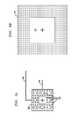
- FIGS. 3A and 3Billustrate a planar patch antenna and a complementary focusing metal element, respectively, which can be used to construct an RFIC package with an integrated antenna structure, according to an embodiment of the invention.
- FIGS. 4A and 4Billustrate a fractal patch antenna and a complementary focusing metal element, respectively, which can be used to construct an RFIC package with an integrated antenna structure, according to another embodiment of the invention.
- FIG. 5schematically depicts an RFIC package comprising an integrated antenna structure according to another embodiment of the invention.
- FIG. 6schematically depicts an RFIC package comprising an integrated antenna structure according to another embodiment of the invention.
- Embodiments of the inventionwill now be discussed in further detail with regard to packaging structures and methods to improve antenna performance (e.g., antenna gain and bandwidth) in millimeter-wave applications (e.g., 94 GHz) for on-chip antennas that are integrally formed as part of BEOL structures of RFIC chips.
- embodiments of the invention as shown in the accompanying drawingsinclude package structures having an antenna structure comprising a planar on-chip antenna, wherein the on-chip antenna comprises one or more planar radiator elements formed as part of a BEOL structure of an RFIC chip.
- the antenna structurefurther comprises a superstrate structure disposed on the BEOL structure of the RFIC chip.
- the superstrate structureincludes at least one substrate layer and a focusing metal element.
- the focusing metal elementhas a structure that is complementary to the on-chip radiator elements, and the focusing metal element is configured to focus electromagnetic radiation to and from the planar on-chip antenna.
- the superstrate structureimproves the performance (e.g., antenna gain and bandwidth) of the on-chip antenna for millimeter-wave applications.
- FIG. 1schematically depicts an RFIC package comprising an integrated antenna structure according to an embodiment of the invention.
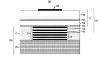
- FIG. 1is a schematic side view of a package structure 100 comprising an RFIC chip 110 and an antenna structure 120 integrally formed on an active side of the RFIC chip 110 .
- the RFIC chip 110comprises a semiconductor substrate 111 (e.g., silicon substrate) and a BEOL structure 112 formed on an active surface of the semiconductor substrate 111 .
- the BEOL structure 112comprises a plurality of alternating dielectric/insulating layers and patterned metallic layers 113 .
- the dielectric/insulating layersmay be formed of materials such as silicon dioxide, and the patterned metallic layers may be formed of materials such as copper, gold, aluminum, or other known dielectric, insulating, metallic or conductor materials, which are commonly used to construct BEOL structures in wafer scale manufacturing.
- the semiconductor substrate 111comprises active circuit elements that form various circuits, such as a receiver, a transmitter, or a transceiver circuit, for example, as well as other types of active or passive circuit elements that are commonly used to implement wireless RFIC chips.
- the BEOL insulating and metal layers 113comprise a plurality of lower metal layers 114 which form an interconnect fabric for connecting the various active and passive circuit components in the active surface of the semiconductor substrate 111 .
- the lower metal layers 114may comprise various patterned structures including, horizontal wiring, vertical interconnects, vias, contact pads, and other passive components such as distributed inductor and capacitor elements, etc. which are commonly used for constructing BEOL interconnection networks.
- the BEOL insulating and metal layers 113further comprise a plurality of upper metal layers 121 and 122 that form various on-chip antenna components of the antenna structure 120 .
- the upper layers of the BEOL layers 113include for example, an antenna ground plane 121 and two or more patterned metal layers 122 that form antenna feed line structures and planar radiator elements.
- the metal layers 121 and 122form an on-chip antenna structure that is fabricated part of the BEOL structure 112 of the RFIC chip 110 .
- the on-chip antenna structureis generically depicted by the patterned metal layers 121 and 122 shown in FIG.
- the various antenna components formed by the patterned metal layers 122may include one or more of various types of planar antenna radiator elements such as patch antennas, stacked patch antennas, electromagnetically-coupled patch antennas, slot antennas, ring antennas, fractal patch antennas, dipole antennas, loop antennas, and other types of planar antenna radiator elements known by those of ordinary skill in the art.
- an antenna feed linemay be a differential feed line, a micro strip line, or a co-planar waveguide line, or other types of feed lines that are directly connected to antenna radiator elements or which electromagnetically couple energy to and from antenna radiator elements.
- an on-chip antenna structure formed by the patterned metal layers 121 and 122 of the BEOL structure 112 alonecan be very poor, with the radiation efficiency (gain) of an on-chip antenna undesirably low, e.g., in a range of about ⁇ 15 dBi to about ⁇ 3 dBi, depending on the antenna design.
- on-chip antenna structuresare problematic in that these structures can couple substantial RF power into substrate modes of various layers of the semiconductor substrate due to the effective electrical thickness of these layers at such millimeter-wave frequencies. These substrate modes not only increase mutual coupling between the on-chip antenna structure and other on-chip components, but also make the impedance and radiation patterns sensitive to the dimensions of the silicon layers and nearby structures.
- the low resistivity (meaning high loss) silicon materialdissipates substantial RF power as loss, resulting in very low antenna radiation efficiency.
- the antenna ground plane 121which is disposed between the semiconductor substrate 111 and the patterned metal layers 122 forming the antenna radiator and feed line elements, can provide some isolation from the lossy material forming the semiconductor substrate 111 , the thickness of the BEOL oxide layers (which are typically ⁇ 12 ⁇ m thick), can degrade the radiation efficiency and performance of the on-chip antenna radiator elements when the radiator elements are too close the ground plane 121 .
- the antenna structure 120 shown in FIG. 1comprises a superstrate structure 127 disposed on top of the BEOL structure 112 .
- the superstrate structure 127comprises a first substrate layer 124 that is bonded to the top of the BEOL structure 112 by a first adhesive layer 123 , a second substrate layer 126 that is bonded to the top of the first substrate layer 124 by a second adhesive layer 125 , and a focusing metallic element 128 disposed on top of the second substrate layer 126 .
- the focusing metallic element 128is aligned to the radiator elements of the on-chip antenna structure 122 . It is to be understood term “aligned” means, for example, that the focusing metallic element 128 and an on-chip antenna radiator element either partially overlap or fully overlap each other on the different layers.
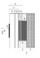
- FIG. 2schematically depicts an RFIC package comprising an integrated antenna structure according to another embodiment of the invention.
- FIG. 2is a schematic side view of a package structure 200 comprising an RFIC chip 110 and an antenna structure 220 integrally formed on an active side of the RFIC chip 110 .
- the various components 111 , 112 , 113 , 114 , 121 , 122 , 123 , and 128 of the RFIC chip 110 and antenna structure 220 depicted in FIG. 2are the same or similar in structure and function to the similarly labeled components shown in FIG. 1 .
- the antenna structure 220 shown in FIG. 2has superstrate structure 227 that comprises a single substrate layer 224 bonded to the BEOL structure 112 with the focusing element 128 disposed on top of the single substrate layer 224 in alignment with the on-chip antenna structure 122 .
- the inventorshave found through experimentation and construction of experimental prototypes, that the performance of an on-chip antenna can be improved with respect to increased antenna bandwidth and increased antenna gain by using a superstrate structure comprising one or more focusing metallic elements disposed on top of a stack of one or more low-loss substrates, as generally depicted in FIGS. 1 and 2 .
- a superstrate structurecomprising one or more focusing metallic elements disposed on top of a stack of one or more low-loss substrates, as generally depicted in FIGS. 1 and 2 .
- the focusing metal elements 128 shown in FIGS. 1 and 2do not function as antenna radiator elements. Instead, the focusing metal elements 128 in FIGS.
- the distance between the on-chip antenna radiator elements and the complementary focusing metal elements 128can vary significantly, resulting in flexibility of the total thickness of the one or substrate layers of the superstrate structures that separate the complementary focusing metal elements 128 and the on-chip radiator elements.
- the distance between the focusing metal element 128 and the on-chip antenna structure 122can be much less than 1 ⁇ 4 wavelength for the given operating frequency.
- the substrate layers 124 , 126 , and 224 of the superstrate structures 127 and 227 shown in FIGS. 1 and 2are formed of low-loss, low dielectric constant materials.
- the substrates 124 , 126 and 224may be formed of a low loss semiconductor substrate material such as high resistivity silicon (e.g., >1000 Ohm ⁇ cm), silica, quartz, or other materials suitable for wafer-scale manufacturing.
- the thickness of the various substrate layers 124 , 126 , and 224will depend on factors such as the dielectric constant of the material used, the operating frequency, the performance requirements (bandwidth, gain) of the antenna structures, and the commercial availability of substrate materials that are desired for the given package structure design.
- the first substrate layer 124is an insulating layer formed of a glass material (e.g., Borofloat) and the second substrate layer 126 is a semiconductor layer formed of high-resistivity silicon.
- a glass materiale.g., Borofloat
- the second substrate layer 126is a semiconductor layer formed of high-resistivity silicon.
- the total thickness of the two substrate layerscan be in a range of about 50 ⁇ m to about 250 ⁇ m, wherein the first substrate layer 124 formed of a glass material such as Borofloat can have a thickness in a range of about 50 ⁇ m to about 100 ⁇ m, and wherein the second substrate layer 126 formed of high-resistivity silicon material can have a thickness in a range of about 50 ⁇ m to about 150 ⁇ m.
- the single substrate layer 224can be formed of a low loss, low dielectric material such as glass having a thickness in a range of about 50 ⁇ m to about 450 ⁇ m.
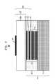
- FIGS. 3A and 3Billustrate embodiments of a planar patch antenna and a complementary focusing metal element, respectively, which can be used to construct an antenna structure for an RFIC package, according to an embodiment of the invention.
- FIG. 3Aschematically illustrates a planar dual-polarized patch antenna 300 with two feed lines 301 and 302 , which can be patterned on an upper metal layer of the BEOL layers 122 (as generically depicted in FIGS. 1 and 2 ) to form an on-chip antenna.
- FIG. 3Bschematically illustrates a planar focusing metal element 310 that is complementary to the patch element 300 of FIG. 3A , and which can be used for the focusing metal element 128 generically depicted in FIGS. 1 and 2 , for example.
- the planar focusing metal element 310 shown in FIG. 3Bcomprises a square cutout feature 311 in a central region thereof, and a plurality of thin, rectangular notch features 312 , 313 , 314 and 315 extending out from each side of the square cutout feature 311 .
- the “+” signs depicted in FIGS. 3A and 3Bare exemplary alignment markers that illustrate how the planar patch antenna element 300 and the complementary planar focusing metal element 310 are vertically aligned with each other in a package structure.
- the planar focusing metal element 310 with the central square cutout feature 311functions as a lens structure that narrows the beam width of the antenna and focuses electromagnetic energy to and from the planar patch antenna element 300 , thereby increasing the gain of the antenna structure.
- the central square cutout feature 311 of the planar focusing metal element 310is slightly larger in area than the planar patch antenna element 300 of FIG. 3A .
- the four thin rectangular notches 312 , 313 , 314 and 315are used to tune the antenna impedance matching.
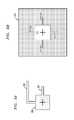
- FIGS. 4A and 4Billustrate embodiments of a planar dual-polarized fractal-patch antenna and a complementary focusing metal element, respectively, which can be used to construct an antenna structure for an RFIC package, according to another embodiment of the invention.
- FIG. 4Aschematically illustrates a planar dual-polarized fractal-patch antenna 400 with two feed lines 401 and 402 , which can be patterned on an upper metal layer of the BEOL layers 122 (as generically depicted in FIGS. 1 and 2 ) to form an on-chip antenna.
- the planar dual-polarized fractal-patch antenna 400comprises a pattern of variable size cutout features 403 , which enables the fractal patch radiator element 400 to have smaller dimensions than the planar patch element 300 of FIG. 3A , for the same operating frequency (e.g. 94 GHz).
- FIG. 4Bschematically illustrates a planar focusing metal element 410 that is complementary to the planar fractal patch antenna element 400 of FIG. 4A , and which can be used for the focusing metal element 128 generically depicted in FIGS. 1 and 2 , for example.
- the planar focusing metal element 410 shown in FIG. 4Bcomprises a square cutout feature 411 in a central region thereof.
- the “+” signs depicted in FIGS. 4A and 4Bare exemplary alignment markers that illustrate how the planar fractal patch antenna element 400 and the complementary planar focusing element 410 are vertically aligned with each other in a package structure.
- the planar focusing metal element 410 with the central square cutout feature 411functions as a lens structure that narrows the beam width of the antenna and focuses electromagnetic energy to and from the planar fractal patch antenna element 400 , thereby increasing the gain of the antenna structure.
- the central square cutout feature 411 of the planar focusing metal element 410is larger in area than the planar fractal patch antenna element 400 of FIG. 4A .
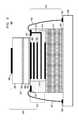
- FIG. 5schematically depicts an RFIC package comprising an integrated antenna structure according to another embodiment of the invention, which implements a TSV (Through-Silicon-Via) design.
- FIG. 5illustrates an RFIC package structure 500 that implements a TSV process which allows the overall RFIC package structure with an integrated antenna to be wafer-scaled manufactured, and therefore, suitable for 3D integration.
- FIG. 5is a side schematic view of a package structure 500 comprising an RFIC chip 510 , an antenna structure 120 integrally formed on an active side of the RFIC chip 510 , and an application board 530 on which the RFIC chip 510 is mounted using a BGA (ball grid array) and C4 process.
- the antenna structure 120 shown in FIG. 5is similar to the antenna structure 120 shown in FIG. 1 , so detailed discussion thereof will not be repeated.
- the RFIC chip 510 of FIG. 5comprises a semiconductor substrate 511 (e.g., silicon substrate) and a BEOL structure 512 formed on an active surface of the semiconductor substrate 511 .
- the BEOL structure 512comprises a plurality of alternating dielectric/insulating layers and patterned metallic layers 513 .
- the RFIC chip 510further comprises a plurality of conductive through-silicon-vias 515 and 516 , which are formed through the BEOL structure 512 and semiconductor substrate 511 , forming vertical interconnects between various patterned metal layers of the BEOL layers 513 to contact pads 517 formed on the backside surface of the semiconductor substrate 511 .
- the silicon-through via 515provides an electrical connection between a contact pad 517 on the backside surface of the substrate 511 to one of the patterned metal layers 122 (e.g., antenna feed line) of the on-chip antenna structure.
- the silicon-through via 516provides an electrical connection between another contact pad 517 and a patterned metal layer (e.g., power plane, I/0 wiring, etc.) of an interconnection network 514 of the BEOL structure 512 .
- the silicon-through vias 515 and 516allow DC supply, or control or I/O baseband signal connections between the RFIC chip 510 and other chip packages or system components mounted to the application board 530 .
- the contact pads 517may be bonded to corresponding contacts (not shown) formed on the application board 530 using BGA techniques and solder balls (e.g., C4 connections).
- An underfill/adhesive layer 532is used to further bond the backside surface of the substrate 511 to the surface of the application board 530 and reduce mechanical stress on the BGA, C4 connections, using well-known techniques.
- a superstrate structurewhen a TSV process is not utilized, can be manufactured separately from an RFIC package with an on-chip antenna, and the two package components can be bonded together in a separate process, and then mounted to an application board with bonding wires, as depicted in FIG. 6 .
- FIG. 6schematically depicts an RFIC package 600 comprising an RFIC chip 610 and a superstrate structure 627 that is manufactured separately from the RFIC chip 610 and then subsequently bonded to the RFIC chip 610 using an adhesive material 623 .
- the footprint size of the RFIC chip 610 and the antenna superstrate structure 627are different, allowing for a different approach to packaging and wiring.
- the footprint size of the RFIC chip 610is greater than the footprint size of the antenna superstrate structure 627 , thereby allowing low frequency wire bonds 635 to be attached to contact pads 617 exposed in a peripheral region of the top surface of a BEOL structure 612 of the RFIC chip 610 and to contact pads 634 on a top surface of an application board 630 .
- the RFIC chip 610 shown in FIG. 6comprises a semiconductor substrate 611 (e.g., silicon substrate) and a BEOL structure 612 formed on an active surface of the semiconductor substrate 611 .
- the BEOL structure 612comprises a plurality of alternating dielectric/insulating layers and patterned metallic layers 613 , vertical interconnects 615 , and upper contact pads 617 exposed on an upper surface of the BEOL structure 612 .
- the vertical interconnect 615comprises a plurality of aligned conductive vias formed through multiple insulating/dielectric layers of the BEOL structure 612 .
- the vertical interconnect 615connects one or more patterned metal layers 614 of the BEOL layers 613 to the contact pads 617 .
- an antenna structure 620comprises on chip antenna structure formed as part of the upper metal layers 621 , 622 of the BEOL layers 613 , and the superstrate structure 627 .
- the superstrate structure 627comprises a first substrate layer 624 bonded to the BEOL structure 612 using the adhesive layer 623 , a second substrate layer 626 bonded to the first substrate layer 624 using an adhesive layer 625 , and a complementary focusing metal element 628 disposed on top of the second substrate layer 626 .
- the superstrate structure 627 shown in FIG. 6is similar in structure and composition to the superstrate structure 127 shown in FIGS.
- the superstrate structure 627has a smaller footprint than the RFIC chip 610 to thereby expose the contact pads 617 formed in the peripheral upper surface region of the BEOL structure 612 .
- the wire bonds 635are implemented to provide electrical connections between the contact pads 617 of the RFIC chip 610 and the contact pads 634 on the application board 630 , which allows direct DC supply and/or control and I/O baseband signal connections between the RFIC chip 610 and other components or package structures or systems connected to the application board 630 .
- the RFIC chip 610is bonded to the application board 630 using an adhesive layer 632 .
- the exemplary package structurecan be readily fabricated using known wafer-scale manufacturing and packaging techniques to fabricate and package antenna structures with semiconductor RFIC chips to form compact integrated radio/wireless communications systems for millimeter-wave and Terahertz applications.
- integrated chip packages according to exemplary embodiments of the inventionenable antennas to be integrally packaged with IC chips such as transceiver chips, which provide compact designs with very low loss between the transceiver and the antenna.
- IC chipssuch as transceiver chips
- Various types of antenna designscan be implemented including patch antennas, slot antennas, slot ring antennas, dipole antennas, and cavity antennas, for example.
- the use of integrated antenna/IC chip packages according to the present inventionsaves significant space, size, cost, and weight, which is a premium for virtually any commercial or military application.
Landscapes
- Engineering & Computer Science (AREA)
- Microelectronics & Electronic Packaging (AREA)
- Waveguide Aerials (AREA)
- Details Of Aerials (AREA)
Abstract
Description
Claims (30)
Priority Applications (1)
| Application Number | Priority Date | Filing Date | Title |
|---|---|---|---|
| US13/686,377US8917210B2 (en) | 2012-11-27 | 2012-11-27 | Package structures to improve on-chip antenna performance |
Applications Claiming Priority (1)
| Application Number | Priority Date | Filing Date | Title |
|---|---|---|---|
| US13/686,377US8917210B2 (en) | 2012-11-27 | 2012-11-27 | Package structures to improve on-chip antenna performance |
Publications (2)
| Publication Number | Publication Date |
|---|---|
| US20140145884A1 US20140145884A1 (en) | 2014-05-29 |
| US8917210B2true US8917210B2 (en) | 2014-12-23 |
Family
ID=50772792
Family Applications (1)
| Application Number | Title | Priority Date | Filing Date |
|---|---|---|---|
| US13/686,377Active2033-06-14US8917210B2 (en) | 2012-11-27 | 2012-11-27 | Package structures to improve on-chip antenna performance |
Country Status (1)
| Country | Link |
|---|---|
| US (1) | US8917210B2 (en) |
Cited By (154)
| Publication number | Priority date | Publication date | Assignee | Title |
|---|---|---|---|---|
| US9608740B2 (en) | 2015-07-15 | 2017-03-28 | At&T Intellectual Property I, L.P. | Method and apparatus for launching a wave mode that mitigates interference |
| US9615269B2 (en) | 2014-10-02 | 2017-04-04 | At&T Intellectual Property I, L.P. | Method and apparatus that provides fault tolerance in a communication network |
| US9628116B2 (en) | 2015-07-14 | 2017-04-18 | At&T Intellectual Property I, L.P. | Apparatus and methods for transmitting wireless signals |
| US9640850B2 (en) | 2015-06-25 | 2017-05-02 | At&T Intellectual Property I, L.P. | Methods and apparatus for inducing a non-fundamental wave mode on a transmission medium |
| US9667317B2 (en) | 2015-06-15 | 2017-05-30 | At&T Intellectual Property I, L.P. | Method and apparatus for providing security using network traffic adjustments |
| US9674711B2 (en) | 2013-11-06 | 2017-06-06 | At&T Intellectual Property I, L.P. | Surface-wave communications and methods thereof |
| US9685992B2 (en) | 2014-10-03 | 2017-06-20 | At&T Intellectual Property I, L.P. | Circuit panel network and methods thereof |
| US9692101B2 (en) | 2014-08-26 | 2017-06-27 | At&T Intellectual Property I, L.P. | Guided wave couplers for coupling electromagnetic waves between a waveguide surface and a surface of a wire |
| US9699785B2 (en) | 2012-12-05 | 2017-07-04 | At&T Intellectual Property I, L.P. | Backhaul link for distributed antenna system |
| US9705561B2 (en) | 2015-04-24 | 2017-07-11 | At&T Intellectual Property I, L.P. | Directional coupling device and methods for use therewith |
| US9705610B2 (en) | 2014-10-21 | 2017-07-11 | At&T Intellectual Property I, L.P. | Transmission device with impairment compensation and methods for use therewith |
| US9722318B2 (en) | 2015-07-14 | 2017-08-01 | At&T Intellectual Property I, L.P. | Method and apparatus for coupling an antenna to a device |
| US9729197B2 (en) | 2015-10-01 | 2017-08-08 | At&T Intellectual Property I, L.P. | Method and apparatus for communicating network management traffic over a network |
| US9735833B2 (en) | 2015-07-31 | 2017-08-15 | At&T Intellectual Property I, L.P. | Method and apparatus for communications management in a neighborhood network |
| US20170237300A1 (en)* | 2012-10-01 | 2017-08-17 | Fractal Antenna Systems, Inc. | Radiative transfer and power control with fractal metamaterial and plasmonics |
| US9742521B2 (en) | 2014-11-20 | 2017-08-22 | At&T Intellectual Property I, L.P. | Transmission device with mode division multiplexing and methods for use therewith |
| US9742462B2 (en) | 2014-12-04 | 2017-08-22 | At&T Intellectual Property I, L.P. | Transmission medium and communication interfaces and methods for use therewith |
| US9749013B2 (en) | 2015-03-17 | 2017-08-29 | At&T Intellectual Property I, L.P. | Method and apparatus for reducing attenuation of electromagnetic waves guided by a transmission medium |
| US9748626B2 (en) | 2015-05-14 | 2017-08-29 | At&T Intellectual Property I, L.P. | Plurality of cables having different cross-sectional shapes which are bundled together to form a transmission medium |
| US9749053B2 (en) | 2015-07-23 | 2017-08-29 | At&T Intellectual Property I, L.P. | Node device, repeater and methods for use therewith |
| US9762289B2 (en) | 2014-10-14 | 2017-09-12 | At&T Intellectual Property I, L.P. | Method and apparatus for transmitting or receiving signals in a transportation system |
| US9769128B2 (en) | 2015-09-28 | 2017-09-19 | At&T Intellectual Property I, L.P. | Method and apparatus for encryption of communications over a network |
| US9769020B2 (en) | 2014-10-21 | 2017-09-19 | At&T Intellectual Property I, L.P. | Method and apparatus for responding to events affecting communications in a communication network |
| US9768833B2 (en) | 2014-09-15 | 2017-09-19 | At&T Intellectual Property I, L.P. | Method and apparatus for sensing a condition in a transmission medium of electromagnetic waves |
| US9780834B2 (en) | 2014-10-21 | 2017-10-03 | At&T Intellectual Property I, L.P. | Method and apparatus for transmitting electromagnetic waves |
| US9787412B2 (en) | 2015-06-25 | 2017-10-10 | At&T Intellectual Property I, L.P. | Methods and apparatus for inducing a fundamental wave mode on a transmission medium |
| US9793951B2 (en) | 2015-07-15 | 2017-10-17 | At&T Intellectual Property I, L.P. | Method and apparatus for launching a wave mode that mitigates interference |
| US9793955B2 (en) | 2015-04-24 | 2017-10-17 | At&T Intellectual Property I, Lp | Passive electrical coupling device and methods for use therewith |
| US9793954B2 (en) | 2015-04-28 | 2017-10-17 | At&T Intellectual Property I, L.P. | Magnetic coupling device and methods for use therewith |
| US9800327B2 (en) | 2014-11-20 | 2017-10-24 | At&T Intellectual Property I, L.P. | Apparatus for controlling operations of a communication device and methods thereof |
| US9820146B2 (en) | 2015-06-12 | 2017-11-14 | At&T Intellectual Property I, L.P. | Method and apparatus for authentication and identity management of communicating devices |
| US9838896B1 (en) | 2016-12-09 | 2017-12-05 | At&T Intellectual Property I, L.P. | Method and apparatus for assessing network coverage |
| US9838078B2 (en) | 2015-07-31 | 2017-12-05 | At&T Intellectual Property I, L.P. | Method and apparatus for exchanging communication signals |
| US9847566B2 (en) | 2015-07-14 | 2017-12-19 | At&T Intellectual Property I, L.P. | Method and apparatus for adjusting a field of a signal to mitigate interference |
| US9847850B2 (en) | 2014-10-14 | 2017-12-19 | At&T Intellectual Property I, L.P. | Method and apparatus for adjusting a mode of communication in a communication network |
| US9853342B2 (en) | 2015-07-14 | 2017-12-26 | At&T Intellectual Property I, L.P. | Dielectric transmission medium connector and methods for use therewith |
| US9860075B1 (en) | 2016-08-26 | 2018-01-02 | At&T Intellectual Property I, L.P. | Method and communication node for broadband distribution |
| US9866309B2 (en) | 2015-06-03 | 2018-01-09 | At&T Intellectual Property I, Lp | Host node device and methods for use therewith |
| US9866276B2 (en) | 2014-10-10 | 2018-01-09 | At&T Intellectual Property I, L.P. | Method and apparatus for arranging communication sessions in a communication system |
| US9865911B2 (en) | 2015-06-25 | 2018-01-09 | At&T Intellectual Property I, L.P. | Waveguide system for slot radiating first electromagnetic waves that are combined into a non-fundamental wave mode second electromagnetic wave on a transmission medium |
| US9871558B2 (en) | 2014-10-21 | 2018-01-16 | At&T Intellectual Property I, L.P. | Guided-wave transmission device and methods for use therewith |
| US9871282B2 (en) | 2015-05-14 | 2018-01-16 | At&T Intellectual Property I, L.P. | At least one transmission medium having a dielectric surface that is covered at least in part by a second dielectric |
| US9871283B2 (en) | 2015-07-23 | 2018-01-16 | At&T Intellectual Property I, Lp | Transmission medium having a dielectric core comprised of plural members connected by a ball and socket configuration |
| US9876605B1 (en) | 2016-10-21 | 2018-01-23 | At&T Intellectual Property I, L.P. | Launcher and coupling system to support desired guided wave mode |
| US9876571B2 (en) | 2015-02-20 | 2018-01-23 | At&T Intellectual Property I, Lp | Guided-wave transmission device with non-fundamental mode propagation and methods for use therewith |
| US9876264B2 (en) | 2015-10-02 | 2018-01-23 | At&T Intellectual Property I, Lp | Communication system, guided wave switch and methods for use therewith |
| US9882257B2 (en) | 2015-07-14 | 2018-01-30 | At&T Intellectual Property I, L.P. | Method and apparatus for launching a wave mode that mitigates interference |
| US9887447B2 (en) | 2015-05-14 | 2018-02-06 | At&T Intellectual Property I, L.P. | Transmission medium having multiple cores and methods for use therewith |
| US9893795B1 (en) | 2016-12-07 | 2018-02-13 | At&T Intellectual Property I, Lp | Method and repeater for broadband distribution |
| US9906269B2 (en) | 2014-09-17 | 2018-02-27 | At&T Intellectual Property I, L.P. | Monitoring and mitigating conditions in a communication network |
| US9904535B2 (en) | 2015-09-14 | 2018-02-27 | At&T Intellectual Property I, L.P. | Method and apparatus for distributing software |
| US9913139B2 (en) | 2015-06-09 | 2018-03-06 | At&T Intellectual Property I, L.P. | Signal fingerprinting for authentication of communicating devices |
| US9912381B2 (en) | 2015-06-03 | 2018-03-06 | At&T Intellectual Property I, Lp | Network termination and methods for use therewith |
| US9912033B2 (en) | 2014-10-21 | 2018-03-06 | At&T Intellectual Property I, Lp | Guided wave coupler, coupling module and methods for use therewith |
| US9912027B2 (en) | 2015-07-23 | 2018-03-06 | At&T Intellectual Property I, L.P. | Method and apparatus for exchanging communication signals |
| US9911020B1 (en) | 2016-12-08 | 2018-03-06 | At&T Intellectual Property I, L.P. | Method and apparatus for tracking via a radio frequency identification device |
| US9912419B1 (en) | 2016-08-24 | 2018-03-06 | At&T Intellectual Property I, L.P. | Method and apparatus for managing a fault in a distributed antenna system |
| US9917341B2 (en) | 2015-05-27 | 2018-03-13 | At&T Intellectual Property I, L.P. | Apparatus and method for launching electromagnetic waves and for modifying radial dimensions of the propagating electromagnetic waves |
| US9930668B2 (en) | 2013-05-31 | 2018-03-27 | At&T Intellectual Property I, L.P. | Remote distributed antenna system |
| US9927517B1 (en) | 2016-12-06 | 2018-03-27 | At&T Intellectual Property I, L.P. | Apparatus and methods for sensing rainfall |
| KR101842861B1 (en)* | 2017-01-03 | 2018-03-28 | 국방과학연구소 | Small rectenna for receiving dual polarization and detecting electromagnetic wave |
| US9948333B2 (en) | 2015-07-23 | 2018-04-17 | At&T Intellectual Property I, L.P. | Method and apparatus for wireless communications to mitigate interference |
| US9948355B2 (en) | 2014-10-21 | 2018-04-17 | At&T Intellectual Property I, L.P. | Apparatus for providing communication services and methods thereof |
| US9948354B2 (en) | 2015-04-28 | 2018-04-17 | At&T Intellectual Property I, L.P. | Magnetic coupling device with reflective plate and methods for use therewith |
| US9954286B2 (en) | 2014-10-21 | 2018-04-24 | At&T Intellectual Property I, L.P. | Guided-wave transmission device with non-fundamental mode propagation and methods for use therewith |
| US9954287B2 (en) | 2014-11-20 | 2018-04-24 | At&T Intellectual Property I, L.P. | Apparatus for converting wireless signals and electromagnetic waves and methods thereof |
| US9967173B2 (en) | 2015-07-31 | 2018-05-08 | At&T Intellectual Property I, L.P. | Method and apparatus for authentication and identity management of communicating devices |
| US9973940B1 (en) | 2017-02-27 | 2018-05-15 | At&T Intellectual Property I, L.P. | Apparatus and methods for dynamic impedance matching of a guided wave launcher |
| US9991580B2 (en) | 2016-10-21 | 2018-06-05 | At&T Intellectual Property I, L.P. | Launcher and coupling system for guided wave mode cancellation |
| US9998870B1 (en) | 2016-12-08 | 2018-06-12 | At&T Intellectual Property I, L.P. | Method and apparatus for proximity sensing |
| US9997819B2 (en) | 2015-06-09 | 2018-06-12 | At&T Intellectual Property I, L.P. | Transmission medium and method for facilitating propagation of electromagnetic waves via a core |
| US9999038B2 (en) | 2013-05-31 | 2018-06-12 | At&T Intellectual Property I, L.P. | Remote distributed antenna system |
| US10009067B2 (en) | 2014-12-04 | 2018-06-26 | At&T Intellectual Property I, L.P. | Method and apparatus for configuring a communication interface |
| US10009065B2 (en) | 2012-12-05 | 2018-06-26 | At&T Intellectual Property I, L.P. | Backhaul link for distributed antenna system |
| US10009063B2 (en) | 2015-09-16 | 2018-06-26 | At&T Intellectual Property I, L.P. | Method and apparatus for use with a radio distributed antenna system having an out-of-band reference signal |
| US10020844B2 (en) | 2016-12-06 | 2018-07-10 | T&T Intellectual Property I, L.P. | Method and apparatus for broadcast communication via guided waves |
| US10027398B2 (en) | 2015-06-11 | 2018-07-17 | At&T Intellectual Property I, Lp | Repeater and methods for use therewith |
| US10027397B2 (en) | 2016-12-07 | 2018-07-17 | At&T Intellectual Property I, L.P. | Distributed antenna system and methods for use therewith |
| US10033107B2 (en) | 2015-07-14 | 2018-07-24 | At&T Intellectual Property I, L.P. | Method and apparatus for coupling an antenna to a device |
| US10033108B2 (en) | 2015-07-14 | 2018-07-24 | At&T Intellectual Property I, L.P. | Apparatus and methods for generating an electromagnetic wave having a wave mode that mitigates interference |
| US10044409B2 (en) | 2015-07-14 | 2018-08-07 | At&T Intellectual Property I, L.P. | Transmission medium and methods for use therewith |
| US10069535B2 (en) | 2016-12-08 | 2018-09-04 | At&T Intellectual Property I, L.P. | Apparatus and methods for launching electromagnetic waves having a certain electric field structure |
| US10079661B2 (en) | 2015-09-16 | 2018-09-18 | At&T Intellectual Property I, L.P. | Method and apparatus for use with a radio distributed antenna system having a clock reference |
| US10090594B2 (en) | 2016-11-23 | 2018-10-02 | At&T Intellectual Property I, L.P. | Antenna system having structural configurations for assembly |
| US10090606B2 (en) | 2015-07-15 | 2018-10-02 | At&T Intellectual Property I, L.P. | Antenna system with dielectric array and methods for use therewith |
| US10103801B2 (en) | 2015-06-03 | 2018-10-16 | At&T Intellectual Property I, L.P. | Host node device and methods for use therewith |
| US10103422B2 (en) | 2016-12-08 | 2018-10-16 | At&T Intellectual Property I, L.P. | Method and apparatus for mounting network devices |
| US10135146B2 (en) | 2016-10-18 | 2018-11-20 | At&T Intellectual Property I, L.P. | Apparatus and methods for launching guided waves via circuits |
| US10135145B2 (en) | 2016-12-06 | 2018-11-20 | At&T Intellectual Property I, L.P. | Apparatus and methods for generating an electromagnetic wave along a transmission medium |
| US10135147B2 (en) | 2016-10-18 | 2018-11-20 | At&T Intellectual Property I, L.P. | Apparatus and methods for launching guided waves via an antenna |
| US10136434B2 (en) | 2015-09-16 | 2018-11-20 | At&T Intellectual Property I, L.P. | Method and apparatus for use with a radio distributed antenna system having an ultra-wideband control channel |
| US10142086B2 (en) | 2015-06-11 | 2018-11-27 | At&T Intellectual Property I, L.P. | Repeater and methods for use therewith |
| US10139820B2 (en) | 2016-12-07 | 2018-11-27 | At&T Intellectual Property I, L.P. | Method and apparatus for deploying equipment of a communication system |
| US20180342472A1 (en)* | 2015-12-22 | 2018-11-29 | Intel Corporation | Microelectronic devices with high frequency communication modules having compound semiconductor devices integrated on a package fabric |
| US10148016B2 (en) | 2015-07-14 | 2018-12-04 | At&T Intellectual Property I, L.P. | Apparatus and methods for communicating utilizing an antenna array |
| US10144036B2 (en) | 2015-01-30 | 2018-12-04 | At&T Intellectual Property I, L.P. | Method and apparatus for mitigating interference affecting a propagation of electromagnetic waves guided by a transmission medium |
| US10168695B2 (en) | 2016-12-07 | 2019-01-01 | At&T Intellectual Property I, L.P. | Method and apparatus for controlling an unmanned aircraft |
| US10170840B2 (en) | 2015-07-14 | 2019-01-01 | At&T Intellectual Property I, L.P. | Apparatus and methods for sending or receiving electromagnetic signals |
| US10178445B2 (en) | 2016-11-23 | 2019-01-08 | At&T Intellectual Property I, L.P. | Methods, devices, and systems for load balancing between a plurality of waveguides |
| US10205655B2 (en) | 2015-07-14 | 2019-02-12 | At&T Intellectual Property I, L.P. | Apparatus and methods for communicating utilizing an antenna array and multiple communication paths |
| US10225025B2 (en) | 2016-11-03 | 2019-03-05 | At&T Intellectual Property I, L.P. | Method and apparatus for detecting a fault in a communication system |
| US10224634B2 (en) | 2016-11-03 | 2019-03-05 | At&T Intellectual Property I, L.P. | Methods and apparatus for adjusting an operational characteristic of an antenna |
| US10243784B2 (en) | 2014-11-20 | 2019-03-26 | At&T Intellectual Property I, L.P. | System for generating topology information and methods thereof |
| US10243270B2 (en) | 2016-12-07 | 2019-03-26 | At&T Intellectual Property I, L.P. | Beam adaptive multi-feed dielectric antenna system and methods for use therewith |
| CN109560379A (en)* | 2018-12-12 | 2019-04-02 | 瑞声光电科技(常州)有限公司 | Antenna system and communicating terminal |
| US10264586B2 (en) | 2016-12-09 | 2019-04-16 | At&T Mobility Ii Llc | Cloud-based packet controller and methods for use therewith |
| US10291334B2 (en) | 2016-11-03 | 2019-05-14 | At&T Intellectual Property I, L.P. | System for detecting a fault in a communication system |
| US10291311B2 (en) | 2016-09-09 | 2019-05-14 | At&T Intellectual Property I, L.P. | Method and apparatus for mitigating a fault in a distributed antenna system |
| US10298293B2 (en) | 2017-03-13 | 2019-05-21 | At&T Intellectual Property I, L.P. | Apparatus of communication utilizing wireless network devices |
| US10305190B2 (en) | 2016-12-01 | 2019-05-28 | At&T Intellectual Property I, L.P. | Reflecting dielectric antenna system and methods for use therewith |
| US10312567B2 (en) | 2016-10-26 | 2019-06-04 | At&T Intellectual Property I, L.P. | Launcher with planar strip antenna and methods for use therewith |
| US10320586B2 (en) | 2015-07-14 | 2019-06-11 | At&T Intellectual Property I, L.P. | Apparatus and methods for generating non-interfering electromagnetic waves on an insulated transmission medium |
| US10326494B2 (en) | 2016-12-06 | 2019-06-18 | At&T Intellectual Property I, L.P. | Apparatus for measurement de-embedding and methods for use therewith |
| US10326689B2 (en) | 2016-12-08 | 2019-06-18 | At&T Intellectual Property I, L.P. | Method and system for providing alternative communication paths |
| US10340603B2 (en) | 2016-11-23 | 2019-07-02 | At&T Intellectual Property I, L.P. | Antenna system having shielded structural configurations for assembly |
| US10340983B2 (en) | 2016-12-09 | 2019-07-02 | At&T Intellectual Property I, L.P. | Method and apparatus for surveying remote sites via guided wave communications |
| US10340600B2 (en) | 2016-10-18 | 2019-07-02 | At&T Intellectual Property I, L.P. | Apparatus and methods for launching guided waves via plural waveguide systems |
| US10340601B2 (en) | 2016-11-23 | 2019-07-02 | At&T Intellectual Property I, L.P. | Multi-antenna system and methods for use therewith |
| US10340573B2 (en) | 2016-10-26 | 2019-07-02 | At&T Intellectual Property I, L.P. | Launcher with cylindrical coupling device and methods for use therewith |
| US10341142B2 (en) | 2015-07-14 | 2019-07-02 | At&T Intellectual Property I, L.P. | Apparatus and methods for generating non-interfering electromagnetic waves on an uninsulated conductor |
| US10355367B2 (en) | 2015-10-16 | 2019-07-16 | At&T Intellectual Property I, L.P. | Antenna structure for exchanging wireless signals |
| US10359749B2 (en) | 2016-12-07 | 2019-07-23 | At&T Intellectual Property I, L.P. | Method and apparatus for utilities management via guided wave communication |
| US10361489B2 (en) | 2016-12-01 | 2019-07-23 | At&T Intellectual Property I, L.P. | Dielectric dish antenna system and methods for use therewith |
| US10374316B2 (en) | 2016-10-21 | 2019-08-06 | At&T Intellectual Property I, L.P. | System and dielectric antenna with non-uniform dielectric |
| US10382976B2 (en) | 2016-12-06 | 2019-08-13 | At&T Intellectual Property I, L.P. | Method and apparatus for managing wireless communications based on communication paths and network device positions |
| US10389037B2 (en) | 2016-12-08 | 2019-08-20 | At&T Intellectual Property I, L.P. | Apparatus and methods for selecting sections of an antenna array and use therewith |
| US10389029B2 (en) | 2016-12-07 | 2019-08-20 | At&T Intellectual Property I, L.P. | Multi-feed dielectric antenna system with core selection and methods for use therewith |
| US10411356B2 (en) | 2016-12-08 | 2019-09-10 | At&T Intellectual Property I, L.P. | Apparatus and methods for selectively targeting communication devices with an antenna array |
| US10439675B2 (en) | 2016-12-06 | 2019-10-08 | At&T Intellectual Property I, L.P. | Method and apparatus for repeating guided wave communication signals |
| US10446936B2 (en) | 2016-12-07 | 2019-10-15 | At&T Intellectual Property I, L.P. | Multi-feed dielectric antenna system and methods for use therewith |
| US10498044B2 (en) | 2016-11-03 | 2019-12-03 | At&T Intellectual Property I, L.P. | Apparatus for configuring a surface of an antenna |
| US10530505B2 (en) | 2016-12-08 | 2020-01-07 | At&T Intellectual Property I, L.P. | Apparatus and methods for launching electromagnetic waves along a transmission medium |
| US10535928B2 (en) | 2016-11-23 | 2020-01-14 | At&T Intellectual Property I, L.P. | Antenna system and methods for use therewith |
| US10547348B2 (en) | 2016-12-07 | 2020-01-28 | At&T Intellectual Property I, L.P. | Method and apparatus for switching transmission mediums in a communication system |
| US10601494B2 (en) | 2016-12-08 | 2020-03-24 | At&T Intellectual Property I, L.P. | Dual-band communication device and method for use therewith |
| US10637149B2 (en) | 2016-12-06 | 2020-04-28 | At&T Intellectual Property I, L.P. | Injection molded dielectric antenna and methods for use therewith |
| US10650940B2 (en) | 2015-05-15 | 2020-05-12 | At&T Intellectual Property I, L.P. | Transmission medium having a conductive material and methods for use therewith |
| US10665942B2 (en) | 2015-10-16 | 2020-05-26 | At&T Intellectual Property I, L.P. | Method and apparatus for adjusting wireless communications |
| US10694379B2 (en) | 2016-12-06 | 2020-06-23 | At&T Intellectual Property I, L.P. | Waveguide system with device-based authentication and methods for use therewith |
| US10727599B2 (en) | 2016-12-06 | 2020-07-28 | At&T Intellectual Property I, L.P. | Launcher with slot antenna and methods for use therewith |
| US10755542B2 (en) | 2016-12-06 | 2020-08-25 | At&T Intellectual Property I, L.P. | Method and apparatus for surveillance via guided wave communication |
| US10777873B2 (en) | 2016-12-08 | 2020-09-15 | At&T Intellectual Property I, L.P. | Method and apparatus for mounting network devices |
| US10797781B2 (en) | 2015-06-03 | 2020-10-06 | At&T Intellectual Property I, L.P. | Client node device and methods for use therewith |
| US10811767B2 (en) | 2016-10-21 | 2020-10-20 | At&T Intellectual Property I, L.P. | System and dielectric antenna with convex dielectric radome |
| US10819035B2 (en) | 2016-12-06 | 2020-10-27 | At&T Intellectual Property I, L.P. | Launcher with helical antenna and methods for use therewith |
| US10840578B2 (en) | 2018-08-09 | 2020-11-17 | Industrial Technology Research Institute | Antenna array module and manufacturing method thereof |
| US10866034B2 (en) | 2012-10-01 | 2020-12-15 | Fractal Antenna Systems, Inc. | Superconducting wire and waveguides with enhanced critical temperature, incorporating fractal plasmonic surfaces |
| US10914534B2 (en) | 2012-10-01 | 2021-02-09 | Fractal Antenna Systems, Inc. | Directional antennas from fractal plasmonic surfaces |
| US10916969B2 (en) | 2016-12-08 | 2021-02-09 | At&T Intellectual Property I, L.P. | Method and apparatus for providing power using an inductive coupling |
| US10938108B2 (en) | 2016-12-08 | 2021-03-02 | At&T Intellectual Property I, L.P. | Frequency selective multi-feed dielectric antenna system and methods for use therewith |
| US11032819B2 (en) | 2016-09-15 | 2021-06-08 | At&T Intellectual Property I, L.P. | Method and apparatus for use with a radio distributed antenna system having a control channel reference signal |
| US11176338B1 (en)* | 2019-11-01 | 2021-11-16 | Bae Systems Information And Electronic Systems Integration Inc. | On-chip RF interrogation for heterogeneous RFIDS |
| US11268771B2 (en) | 2012-10-01 | 2022-03-08 | Fractal Antenna Systems, Inc. | Enhanced gain antenna systems employing fractal metamaterials |
| US11322850B1 (en) | 2012-10-01 | 2022-05-03 | Fractal Antenna Systems, Inc. | Deflective electromagnetic shielding |
Families Citing this family (151)
| Publication number | Priority date | Publication date | Assignee | Title |
|---|---|---|---|---|
| US10206185B2 (en) | 2013-05-10 | 2019-02-12 | Energous Corporation | System and methods for wireless power transmission to an electronic device in accordance with user-defined restrictions |
| US9859797B1 (en) | 2014-05-07 | 2018-01-02 | Energous Corporation | Synchronous rectifier design for wireless power receiver |
| US20150326070A1 (en) | 2014-05-07 | 2015-11-12 | Energous Corporation | Methods and Systems for Maximum Power Point Transfer in Receivers |
| US10063064B1 (en) | 2014-05-23 | 2018-08-28 | Energous Corporation | System and method for generating a power receiver identifier in a wireless power network |
| US10965164B2 (en) | 2012-07-06 | 2021-03-30 | Energous Corporation | Systems and methods of wirelessly delivering power to a receiver device |
| US9438045B1 (en) | 2013-05-10 | 2016-09-06 | Energous Corporation | Methods and systems for maximum power point transfer in receivers |
| US10141791B2 (en) | 2014-05-07 | 2018-11-27 | Energous Corporation | Systems and methods for controlling communications during wireless transmission of power using application programming interfaces |
| US10186913B2 (en) | 2012-07-06 | 2019-01-22 | Energous Corporation | System and methods for pocket-forming based on constructive and destructive interferences to power one or more wireless power receivers using a wireless power transmitter including a plurality of antennas |
| US10243414B1 (en) | 2014-05-07 | 2019-03-26 | Energous Corporation | Wearable device with wireless power and payload receiver |
| US10148097B1 (en) | 2013-11-08 | 2018-12-04 | Energous Corporation | Systems and methods for using a predetermined number of communication channels of a wireless power transmitter to communicate with different wireless power receivers |
| US10063105B2 (en) | 2013-07-11 | 2018-08-28 | Energous Corporation | Proximity transmitters for wireless power charging systems |
| US10218227B2 (en) | 2014-05-07 | 2019-02-26 | Energous Corporation | Compact PIFA antenna |
| US10063106B2 (en) | 2014-05-23 | 2018-08-28 | Energous Corporation | System and method for a self-system analysis in a wireless power transmission network |
| US9876394B1 (en) | 2014-05-07 | 2018-01-23 | Energous Corporation | Boost-charger-boost system for enhanced power delivery |
| US10038337B1 (en) | 2013-09-16 | 2018-07-31 | Energous Corporation | Wireless power supply for rescue devices |
| US10211680B2 (en) | 2013-07-19 | 2019-02-19 | Energous Corporation | Method for 3 dimensional pocket-forming |
| US11502551B2 (en) | 2012-07-06 | 2022-11-15 | Energous Corporation | Wirelessly charging multiple wireless-power receivers using different subsets of an antenna array to focus energy at different locations |
| US10992187B2 (en) | 2012-07-06 | 2021-04-27 | Energous Corporation | System and methods of using electromagnetic waves to wirelessly deliver power to electronic devices |
| US10256657B2 (en) | 2015-12-24 | 2019-04-09 | Energous Corporation | Antenna having coaxial structure for near field wireless power charging |
| US9825674B1 (en) | 2014-05-23 | 2017-11-21 | Energous Corporation | Enhanced transmitter that selects configurations of antenna elements for performing wireless power transmission and receiving functions |
| US10230266B1 (en) | 2014-02-06 | 2019-03-12 | Energous Corporation | Wireless power receivers that communicate status data indicating wireless power transmission effectiveness with a transmitter using a built-in communications component of a mobile device, and methods of use thereof |
| US10199835B2 (en) | 2015-12-29 | 2019-02-05 | Energous Corporation | Radar motion detection using stepped frequency in wireless power transmission system |
| US10263432B1 (en) | 2013-06-25 | 2019-04-16 | Energous Corporation | Multi-mode transmitter with an antenna array for delivering wireless power and providing Wi-Fi access |
| US10270261B2 (en) | 2015-09-16 | 2019-04-23 | Energous Corporation | Systems and methods of object detection in wireless power charging systems |
| US10291055B1 (en) | 2014-12-29 | 2019-05-14 | Energous Corporation | Systems and methods for controlling far-field wireless power transmission based on battery power levels of a receiving device |
| US10090699B1 (en) | 2013-11-01 | 2018-10-02 | Energous Corporation | Wireless powered house |
| US10211674B1 (en) | 2013-06-12 | 2019-02-19 | Energous Corporation | Wireless charging using selected reflectors |
| US10205239B1 (en) | 2014-05-07 | 2019-02-12 | Energous Corporation | Compact PIFA antenna |
| US9124125B2 (en) | 2013-05-10 | 2015-09-01 | Energous Corporation | Wireless power transmission with selective range |
| US10124754B1 (en) | 2013-07-19 | 2018-11-13 | Energous Corporation | Wireless charging and powering of electronic sensors in a vehicle |
| US9867062B1 (en) | 2014-07-21 | 2018-01-09 | Energous Corporation | System and methods for using a remote server to authorize a receiving device that has requested wireless power and to determine whether another receiving device should request wireless power in a wireless power transmission system |
| US10224758B2 (en) | 2013-05-10 | 2019-03-05 | Energous Corporation | Wireless powering of electronic devices with selective delivery range |
| US10128693B2 (en) | 2014-07-14 | 2018-11-13 | Energous Corporation | System and method for providing health safety in a wireless power transmission system |
| US9871398B1 (en) | 2013-07-01 | 2018-01-16 | Energous Corporation | Hybrid charging method for wireless power transmission based on pocket-forming |
| US10141768B2 (en) | 2013-06-03 | 2018-11-27 | Energous Corporation | Systems and methods for maximizing wireless power transfer efficiency by instructing a user to change a receiver device's position |
| US9843201B1 (en) | 2012-07-06 | 2017-12-12 | Energous Corporation | Wireless power transmitter that selects antenna sets for transmitting wireless power to a receiver based on location of the receiver, and methods of use thereof |
| US10312715B2 (en) | 2015-09-16 | 2019-06-04 | Energous Corporation | Systems and methods for wireless power charging |
| US9887584B1 (en) | 2014-08-21 | 2018-02-06 | Energous Corporation | Systems and methods for a configuration web service to provide configuration of a wireless power transmitter within a wireless power transmission system |
| US12057715B2 (en) | 2012-07-06 | 2024-08-06 | Energous Corporation | Systems and methods of wirelessly delivering power to a wireless-power receiver device in response to a change of orientation of the wireless-power receiver device |
| US10090886B1 (en) | 2014-07-14 | 2018-10-02 | Energous Corporation | System and method for enabling automatic charging schedules in a wireless power network to one or more devices |
| US9812890B1 (en) | 2013-07-11 | 2017-11-07 | Energous Corporation | Portable wireless charging pad |
| US10211682B2 (en) | 2014-05-07 | 2019-02-19 | Energous Corporation | Systems and methods for controlling operation of a transmitter of a wireless power network based on user instructions received from an authenticated computing device powered or charged by a receiver of the wireless power network |
| US10193396B1 (en) | 2014-05-07 | 2019-01-29 | Energous Corporation | Cluster management of transmitters in a wireless power transmission system |
| US10008889B2 (en) | 2014-08-21 | 2018-06-26 | Energous Corporation | Method for automatically testing the operational status of a wireless power receiver in a wireless power transmission system |
| US10128699B2 (en) | 2014-07-14 | 2018-11-13 | Energous Corporation | Systems and methods of providing wireless power using receiver device sensor inputs |
| US10291066B1 (en) | 2014-05-07 | 2019-05-14 | Energous Corporation | Power transmission control systems and methods |
| US10199849B1 (en) | 2014-08-21 | 2019-02-05 | Energous Corporation | Method for automatically testing the operational status of a wireless power receiver in a wireless power transmission system |
| US10381880B2 (en) | 2014-07-21 | 2019-08-13 | Energous Corporation | Integrated antenna structure arrays for wireless power transmission |
| US9787103B1 (en) | 2013-08-06 | 2017-10-10 | Energous Corporation | Systems and methods for wirelessly delivering power to electronic devices that are unable to communicate with a transmitter |
| US10103582B2 (en) | 2012-07-06 | 2018-10-16 | Energous Corporation | Transmitters for wireless power transmission |
| US9853458B1 (en) | 2014-05-07 | 2017-12-26 | Energous Corporation | Systems and methods for device and power receiver pairing |
| US10223717B1 (en) | 2014-05-23 | 2019-03-05 | Energous Corporation | Systems and methods for payment-based authorization of wireless power transmission service |
| US10439448B2 (en) | 2014-08-21 | 2019-10-08 | Energous Corporation | Systems and methods for automatically testing the communication between wireless power transmitter and wireless power receiver |
| US10992185B2 (en) | 2012-07-06 | 2021-04-27 | Energous Corporation | Systems and methods of using electromagnetic waves to wirelessly deliver power to game controllers |
| US10103552B1 (en) | 2013-06-03 | 2018-10-16 | Energous Corporation | Protocols for authenticated wireless power transmission |
| US10021523B2 (en) | 2013-07-11 | 2018-07-10 | Energous Corporation | Proximity transmitters for wireless power charging systems |
| US10075017B2 (en) | 2014-02-06 | 2018-09-11 | Energous Corporation | External or internal wireless power receiver with spaced-apart antenna elements for charging or powering mobile devices using wirelessly delivered power |
| US10158257B2 (en) | 2014-05-01 | 2018-12-18 | Energous Corporation | System and methods for using sound waves to wirelessly deliver power to electronic devices |
| US10153653B1 (en) | 2014-05-07 | 2018-12-11 | Energous Corporation | Systems and methods for using application programming interfaces to control communications between a transmitter and a receiver |
| US10170917B1 (en) | 2014-05-07 | 2019-01-01 | Energous Corporation | Systems and methods for managing and controlling a wireless power network by establishing time intervals during which receivers communicate with a transmitter |
| US10153645B1 (en) | 2014-05-07 | 2018-12-11 | Energous Corporation | Systems and methods for designating a master power transmitter in a cluster of wireless power transmitters |
| US9652649B2 (en)* | 2014-07-02 | 2017-05-16 | Auden Techno Corp. | Chip-type antenna device and chip structure |
| US10116143B1 (en) | 2014-07-21 | 2018-10-30 | Energous Corporation | Integrated antenna arrays for wireless power transmission |
| US10068703B1 (en) | 2014-07-21 | 2018-09-04 | Energous Corporation | Integrated miniature PIFA with artificial magnetic conductor metamaterials |
| US9620464B2 (en) | 2014-08-13 | 2017-04-11 | International Business Machines Corporation | Wireless communications package with integrated antennas and air cavity |
| US10770802B2 (en)* | 2014-11-10 | 2020-09-08 | Qorvo Us, Inc. | Antenna on a device assembly |
| US10122415B2 (en) | 2014-12-27 | 2018-11-06 | Energous Corporation | Systems and methods for assigning a set of antennas of a wireless power transmitter to a wireless power receiver based on a location of the wireless power receiver |
| WO2016130090A1 (en)* | 2015-02-13 | 2016-08-18 | Nanyang Technological University | Semiconductor arrangement and method for fabricating thereof |
| US12283828B2 (en) | 2015-09-15 | 2025-04-22 | Energous Corporation | Receiver devices configured to determine location within a transmission field |
| US10523033B2 (en) | 2015-09-15 | 2019-12-31 | Energous Corporation | Receiver devices configured to determine location within a transmission field |
| US10778041B2 (en) | 2015-09-16 | 2020-09-15 | Energous Corporation | Systems and methods for generating power waves in a wireless power transmission system |
| US9871387B1 (en) | 2015-09-16 | 2018-01-16 | Energous Corporation | Systems and methods of object detection using one or more video cameras in wireless power charging systems |
| US10158259B1 (en) | 2015-09-16 | 2018-12-18 | Energous Corporation | Systems and methods for identifying receivers in a transmission field by transmitting exploratory power waves towards different segments of a transmission field |
| US10199850B2 (en) | 2015-09-16 | 2019-02-05 | Energous Corporation | Systems and methods for wirelessly transmitting power from a transmitter to a receiver by determining refined locations of the receiver in a segmented transmission field associated with the transmitter |
| US10186893B2 (en) | 2015-09-16 | 2019-01-22 | Energous Corporation | Systems and methods for real time or near real time wireless communications between a wireless power transmitter and a wireless power receiver |
| US11710321B2 (en) | 2015-09-16 | 2023-07-25 | Energous Corporation | Systems and methods of object detection in wireless power charging systems |
| US10211685B2 (en) | 2015-09-16 | 2019-02-19 | Energous Corporation | Systems and methods for real or near real time wireless communications between a wireless power transmitter and a wireless power receiver |
| US10008875B1 (en) | 2015-09-16 | 2018-06-26 | Energous Corporation | Wireless power transmitter configured to transmit power waves to a predicted location of a moving wireless power receiver |
| US10020678B1 (en) | 2015-09-22 | 2018-07-10 | Energous Corporation | Systems and methods for selecting antennas to generate and transmit power transmission waves |
| US10135295B2 (en) | 2015-09-22 | 2018-11-20 | Energous Corporation | Systems and methods for nullifying energy levels for wireless power transmission waves |
| US10050470B1 (en) | 2015-09-22 | 2018-08-14 | Energous Corporation | Wireless power transmission device having antennas oriented in three dimensions |
| US10033222B1 (en) | 2015-09-22 | 2018-07-24 | Energous Corporation | Systems and methods for determining and generating a waveform for wireless power transmission waves |
| US10128686B1 (en) | 2015-09-22 | 2018-11-13 | Energous Corporation | Systems and methods for identifying receiver locations using sensor technologies |
| US10027168B2 (en) | 2015-09-22 | 2018-07-17 | Energous Corporation | Systems and methods for generating and transmitting wireless power transmission waves using antennas having a spacing that is selected by the transmitter |
| US10153660B1 (en) | 2015-09-22 | 2018-12-11 | Energous Corporation | Systems and methods for preconfiguring sensor data for wireless charging systems |
| US10135294B1 (en) | 2015-09-22 | 2018-11-20 | Energous Corporation | Systems and methods for preconfiguring transmission devices for power wave transmissions based on location data of one or more receivers |
| CN105305040A (en)* | 2015-09-25 | 2016-02-03 | 西安电子科技大学 | Antenna used for anti-metal tag and signal transmitting and receiving method of antenna |
| US10734717B2 (en) | 2015-10-13 | 2020-08-04 | Energous Corporation | 3D ceramic mold antenna |
| US10333332B1 (en) | 2015-10-13 | 2019-06-25 | Energous Corporation | Cross-polarized dipole antenna |
| US9853485B2 (en) | 2015-10-28 | 2017-12-26 | Energous Corporation | Antenna for wireless charging systems |
| US10135112B1 (en) | 2015-11-02 | 2018-11-20 | Energous Corporation | 3D antenna mount |
| US10063108B1 (en) | 2015-11-02 | 2018-08-28 | Energous Corporation | Stamped three-dimensional antenna |
| US10027180B1 (en) | 2015-11-02 | 2018-07-17 | Energous Corporation | 3D triple linear antenna that acts as heat sink |
| US9832867B2 (en) | 2015-11-23 | 2017-11-28 | Medtronic, Inc. | Embedded metallic structures in glass |
| WO2017111769A1 (en)* | 2015-12-22 | 2017-06-29 | Intel Corporation | Microelectronic devices designed with compound semiconductor devices and integrated on an inter die fabric |
| US10038332B1 (en) | 2015-12-24 | 2018-07-31 | Energous Corporation | Systems and methods of wireless power charging through multiple receiving devices |
| US11863001B2 (en) | 2015-12-24 | 2024-01-02 | Energous Corporation | Near-field antenna for wireless power transmission with antenna elements that follow meandering patterns |
| US10079515B2 (en) | 2016-12-12 | 2018-09-18 | Energous Corporation | Near-field RF charging pad with multi-band antenna element with adaptive loading to efficiently charge an electronic device at any position on the pad |
| US10320446B2 (en) | 2015-12-24 | 2019-06-11 | Energous Corporation | Miniaturized highly-efficient designs for near-field power transfer system |
| US10027159B2 (en) | 2015-12-24 | 2018-07-17 | Energous Corporation | Antenna for transmitting wireless power signals |
| US10186892B2 (en) | 2015-12-24 | 2019-01-22 | Energous Corporation | Receiver device with antennas positioned in gaps |
| US10256677B2 (en) | 2016-12-12 | 2019-04-09 | Energous Corporation | Near-field RF charging pad with adaptive loading to efficiently charge an electronic device at any position on the pad |
| US10164478B2 (en) | 2015-12-29 | 2018-12-25 | Energous Corporation | Modular antenna boards in wireless power transmission systems |
| US10847889B2 (en) | 2016-06-30 | 2020-11-24 | Intel Corporation | Patch antenna with isolated feeds |
| CN106299645A (en)* | 2016-08-22 | 2017-01-04 | 北京无线电测量研究所 | A kind of on-chip antenna based on silicon technology |
| US10923954B2 (en) | 2016-11-03 | 2021-02-16 | Energous Corporation | Wireless power receiver with a synchronous rectifier |
| US10594019B2 (en) | 2016-12-03 | 2020-03-17 | International Business Machines Corporation | Wireless communications package with integrated antenna array |
| CN116455101A (en) | 2016-12-12 | 2023-07-18 | 艾诺格思公司 | Transmitter integrated circuit |
| US10389161B2 (en) | 2017-03-15 | 2019-08-20 | Energous Corporation | Surface mount dielectric antennas for wireless power transmitters |
| US10439442B2 (en) | 2017-01-24 | 2019-10-08 | Energous Corporation | Microstrip antennas for wireless power transmitters |
| US10680319B2 (en) | 2017-01-06 | 2020-06-09 | Energous Corporation | Devices and methods for reducing mutual coupling effects in wireless power transmission systems |
| US11011942B2 (en) | 2017-03-30 | 2021-05-18 | Energous Corporation | Flat antennas having two or more resonant frequencies for use in wireless power transmission systems |
| US20180294569A1 (en)* | 2017-04-07 | 2018-10-11 | Skyworks Solutions, Inc. | Radio-frequency module with integrated shield layer antenna and integrated cavity-based antenna |
| US11069978B2 (en) | 2017-04-07 | 2021-07-20 | Skyworks Solutions, Inc. | Method of manufacturing a radio-frequency module with a conformal shield antenna |
| US10511097B2 (en) | 2017-05-12 | 2019-12-17 | Energous Corporation | Near-field antennas for accumulating energy at a near-field distance with minimal far-field gain |
| US12074452B2 (en) | 2017-05-16 | 2024-08-27 | Wireless Electrical Grid Lan, Wigl Inc. | Networked wireless charging system |
| US12074460B2 (en) | 2017-05-16 | 2024-08-27 | Wireless Electrical Grid Lan, Wigl Inc. | Rechargeable wireless power bank and method of using |
| US11462949B2 (en) | 2017-05-16 | 2022-10-04 | Wireless electrical Grid LAN, WiGL Inc | Wireless charging method and system |
| US10910329B2 (en)* | 2017-05-23 | 2021-02-02 | Advanced Semiconductor Engineering, Inc. | Semiconductor package device and method of manufacturing the same |
| US10848853B2 (en) | 2017-06-23 | 2020-11-24 | Energous Corporation | Systems, methods, and devices for utilizing a wire of a sound-producing device as an antenna for receipt of wirelessly delivered power |
| EP3429026B1 (en)* | 2017-07-10 | 2020-12-02 | Nxp B.V. | An integrated circuit package and method of making thereof |
| US10685924B2 (en)* | 2017-08-24 | 2020-06-16 | Qualcomm Incorporated | Antenna-on-package arrangements |
| US10122219B1 (en) | 2017-10-10 | 2018-11-06 | Energous Corporation | Systems, methods, and devices for using a battery as a antenna for receiving wirelessly delivered power from radio frequency power waves |
| US11342798B2 (en) | 2017-10-30 | 2022-05-24 | Energous Corporation | Systems and methods for managing coexistence of wireless-power signals and data signals operating in a same frequency band |
| US10615647B2 (en) | 2018-02-02 | 2020-04-07 | Energous Corporation | Systems and methods for detecting wireless power receivers and other objects at a near-field charging pad |
| US11159057B2 (en) | 2018-03-14 | 2021-10-26 | Energous Corporation | Loop antennas with selectively-activated feeds to control propagation patterns of wireless power signals |
| US10187019B1 (en) | 2018-03-26 | 2019-01-22 | Qorvo Us, Inc. | Phased array antenna system |
| US11515732B2 (en) | 2018-06-25 | 2022-11-29 | Energous Corporation | Power wave transmission techniques to focus wirelessly delivered power at a receiving device |
| US11437735B2 (en) | 2018-11-14 | 2022-09-06 | Energous Corporation | Systems for receiving electromagnetic energy using antennas that are minimally affected by the presence of the human body |
| EP3918691A1 (en) | 2019-01-28 | 2021-12-08 | Energous Corporation | Systems and methods for miniaturized antenna for wireless power transmissions |
| US11018779B2 (en) | 2019-02-06 | 2021-05-25 | Energous Corporation | Systems and methods of estimating optimal phases to use for individual antennas in an antenna array |
| US12155231B2 (en) | 2019-04-09 | 2024-11-26 | Energous Corporation | Asymmetric spiral antennas for wireless power transmission and reception |
| KR102689200B1 (en)* | 2019-04-12 | 2024-07-29 | 삼성전자 주식회사 | An antenna module and an electronic device including the antenna module |
| CN110148587B (en)* | 2019-06-06 | 2023-09-08 | 盛合晶微半导体(江阴)有限公司 | Fan-out type antenna packaging structure and packaging method |
| CN110350293B (en)* | 2019-06-26 | 2024-11-05 | 加特兰微电子科技(上海)有限公司 | Antenna and radar system on a chip |
| EP4032166A4 (en) | 2019-09-20 | 2023-10-18 | Energous Corporation | SYSTEMS AND METHODS FOR PROTECTING WIRELESS POWER RECEIVER USING MULTIPLE RECTIFIERS AND PRODUCING IN-BAND COMMUNICATION USING MULTIPLE RECTIFIERS |
| WO2021055901A1 (en) | 2019-09-20 | 2021-03-25 | Energous Corporation | Asymmetric spiral antennas with parasitic elements for wireless power transmission |
| US11381118B2 (en) | 2019-09-20 | 2022-07-05 | Energous Corporation | Systems and methods for machine learning based foreign object detection for wireless power transmission |
| US11139699B2 (en) | 2019-09-20 | 2021-10-05 | Energous Corporation | Classifying and detecting foreign objects using a power amplifier controller integrated circuit in wireless power transmission systems |
| WO2021055898A1 (en) | 2019-09-20 | 2021-03-25 | Energous Corporation | Systems and methods for machine learning based foreign object detection for wireless power transmission |
| EP4073905A4 (en) | 2019-12-13 | 2024-01-03 | Energous Corporation | CHARGING STATION HAVING GUIDANCE CONTOURS FOR ALIGNING AN ELECTRONIC DEVICE TO THE CHARGING STATION AND EFFECTIVELY TRANSFERRING NEAR-FIELD RADIO FREQUENCY ENERGY TO THE ELECTRONIC DEVICE |
| US10985617B1 (en) | 2019-12-31 | 2021-04-20 | Energous Corporation | System for wirelessly transmitting energy at a near-field distance without using beam-forming control |
| US11799324B2 (en) | 2020-04-13 | 2023-10-24 | Energous Corporation | Wireless-power transmitting device for creating a uniform near-field charging area |
| US11469629B2 (en) | 2020-08-12 | 2022-10-11 | Energous Corporation | Systems and methods for secure wireless transmission of power using unidirectional communication signals from a wireless-power-receiving device |
| EP4244934B1 (en)* | 2020-11-13 | 2024-10-16 | Viasat Inc. | Integrated antenna array with beamformer ic chips having multiple surface interfaces |
| US12306285B2 (en) | 2020-12-01 | 2025-05-20 | Energous Corporation | Systems and methods for using one or more sensors to detect and classify objects in a keep-out zone of a wireless-power transmission field, and antennas with integrated sensor arrangements |
| CN112909531B (en)* | 2021-02-24 | 2022-05-03 | 电子科技大学 | An L-shaped wide-bandwidth beam circularly polarized on-chip antenna for millimeter-wave frequency band |
| CN113193333B (en)* | 2021-04-29 | 2022-10-11 | 电子科技大学 | Fractal structure on-chip antenna applied to CMOS (complementary Metal oxide semiconductor) process |
| US11916398B2 (en) | 2021-12-29 | 2024-02-27 | Energous Corporation | Small form-factor devices with integrated and modular harvesting receivers, and shelving-mounted wireless-power transmitters for use therewith |
| US12142939B2 (en) | 2022-05-13 | 2024-11-12 | Energous Corporation | Integrated wireless-power-transmission platform designed to operate in multiple bands, and multi-band antennas for use therewith |
| CN120237411A (en)* | 2025-05-29 | 2025-07-01 | 杭州市北京航空航天大学国际创新研究院(北京航空航天大学国际创新学院) | On-chip antenna and pulse source integrated device and method based on heterogeneous material 3D packaging integration |
Citations (10)
| Publication number | Priority date | Publication date | Assignee | Title |
|---|---|---|---|---|
| US20040090370A1 (en)* | 2002-11-08 | 2004-05-13 | Kvh Industries, Inc. | Feed network and method for an offset stacked patch antenna array |
| KR20070016691A (en) | 2005-08-05 | 2007-02-08 | (주)하이게인안테나 | Low Altitude Active Radar Antenna |
| EP1858162A1 (en) | 2006-05-17 | 2007-11-21 | Samsung Electronics Co., Ltd. | Device for improving amplitude imbalance of on-chip transformer balun |
| US20090251362A1 (en) | 2008-04-04 | 2009-10-08 | Alexandros Margomenos | Three dimensional integrated automotive radars and methods of manufacturing the same |
| US20090273517A1 (en) | 2008-05-01 | 2009-11-05 | Emag Technologies, Inc. | Vertically integrated electronically steered phased array and method for packaging |
| US20100052975A1 (en) | 2007-08-09 | 2010-03-04 | Beam Networks Ltd. | Compact active phased array antenna for radars |
| GB2467325A (en) | 2009-01-29 | 2010-08-04 | Antenova Ltd | Radio-antenna modules for connection to external matching circuits |
| US20120235881A1 (en) | 2011-03-15 | 2012-09-20 | Pan Helen K | Mm-wave phased array antenna and system integration on semi-flex packaging |
| US20130021208A1 (en)* | 2011-07-22 | 2013-01-24 | Texas Instruments Incorporated | Loop antenna |
| US8384596B2 (en)* | 2008-06-19 | 2013-02-26 | Broadcom Corporation | Method and system for inter-chip communication via integrated circuit package antennas |
- 2012
- 2012-11-27USUS13/686,377patent/US8917210B2/enactiveActive
Patent Citations (10)
| Publication number | Priority date | Publication date | Assignee | Title |
|---|---|---|---|---|
| US20040090370A1 (en)* | 2002-11-08 | 2004-05-13 | Kvh Industries, Inc. | Feed network and method for an offset stacked patch antenna array |
| KR20070016691A (en) | 2005-08-05 | 2007-02-08 | (주)하이게인안테나 | Low Altitude Active Radar Antenna |
| EP1858162A1 (en) | 2006-05-17 | 2007-11-21 | Samsung Electronics Co., Ltd. | Device for improving amplitude imbalance of on-chip transformer balun |
| US20100052975A1 (en) | 2007-08-09 | 2010-03-04 | Beam Networks Ltd. | Compact active phased array antenna for radars |
| US20090251362A1 (en) | 2008-04-04 | 2009-10-08 | Alexandros Margomenos | Three dimensional integrated automotive radars and methods of manufacturing the same |
| US20090273517A1 (en) | 2008-05-01 | 2009-11-05 | Emag Technologies, Inc. | Vertically integrated electronically steered phased array and method for packaging |
| US8384596B2 (en)* | 2008-06-19 | 2013-02-26 | Broadcom Corporation | Method and system for inter-chip communication via integrated circuit package antennas |
| GB2467325A (en) | 2009-01-29 | 2010-08-04 | Antenova Ltd | Radio-antenna modules for connection to external matching circuits |
| US20120235881A1 (en) | 2011-03-15 | 2012-09-20 | Pan Helen K | Mm-wave phased array antenna and system integration on semi-flex packaging |
| US20130021208A1 (en)* | 2011-07-22 | 2013-01-24 | Texas Instruments Incorporated | Loop antenna |
Non-Patent Citations (5)
| Title |
|---|
| A. Babakhani et al., "A 77-GHz Phased-Array Transceiver with On-Chip Antennas in Silicon: Receiver and Antennas," IEEE Journal of Solid-State Circuits, Dec. 2006, pp. 2795-2806, vol. 41, No. 12. |
| A.M. Hashim et al., "Dual-Functional On-Chip AIGaAs/GaAs Schottky Diode for RF Power Detection and Low-Power Rectenna Applications," Sensors, 2011, pp. 8127-8142, vol. 11, No. 8, Molecular Diversity Preservation International. |
| C. Chansungsan et al., "Method for an On-Chip RF CMOS Global Clock Transmitter and Receiver," IP.com Prior Art Database, IPCOM000009611D, Sep. 2002, 5 pages. |
| J.M. Edwards et al., "High-Efficiency Elliptical Slot Antennas with Quartz Superstrates for Silicon RFICs," IEEE Transactions on Antennas and Propagation, Jan. 2012, pp. 1-11. |
| Y.-C. Ou et al., "Differential Microstrip and Slot-Ring Antennas for Millimeter-Wave Silicon Systems," IEEE Transactions on Antennas and Propagation, Jun. 2012, pp. 2611-2619, vol. 60, No. 6. |
Cited By (189)
| Publication number | Priority date | Publication date | Assignee | Title |
|---|---|---|---|---|
| US11322850B1 (en) | 2012-10-01 | 2022-05-03 | Fractal Antenna Systems, Inc. | Deflective electromagnetic shielding |
| US10788272B1 (en) | 2012-10-01 | 2020-09-29 | Fractal Antenna Systems, Inc. | Radiative transfer and power control with fractal metamaterial and plasmonics |
| US10415896B2 (en) | 2012-10-01 | 2019-09-17 | Fractal Antenna Systems, Inc. | Radiative transfer and power control with fractal metamaterial and plasmonics |
| US10866034B2 (en) | 2012-10-01 | 2020-12-15 | Fractal Antenna Systems, Inc. | Superconducting wire and waveguides with enhanced critical temperature, incorporating fractal plasmonic surfaces |
| US10876803B2 (en) | 2012-10-01 | 2020-12-29 | Fractal Antenna Systems, Inc. | Radiative transfer and power control with fractal metamaterial and plasmonics |
| US9935503B2 (en)* | 2012-10-01 | 2018-04-03 | Fractal Antenna Systems, Inc. | Radiative transfer and power control with fractal metamaterial and plasmonics |
| US10914534B2 (en) | 2012-10-01 | 2021-02-09 | Fractal Antenna Systems, Inc. | Directional antennas from fractal plasmonic surfaces |
| US11150035B2 (en) | 2012-10-01 | 2021-10-19 | Fractal Antenna Systems, Inc. | Superconducting wire and waveguides with enhanced critical temperature, incorporating fractal plasmonic surfaces |
| US20170237300A1 (en)* | 2012-10-01 | 2017-08-17 | Fractal Antenna Systems, Inc. | Radiative transfer and power control with fractal metamaterial and plasmonics |
| US11268771B2 (en) | 2012-10-01 | 2022-03-08 | Fractal Antenna Systems, Inc. | Enhanced gain antenna systems employing fractal metamaterials |
| US10194437B2 (en) | 2012-12-05 | 2019-01-29 | At&T Intellectual Property I, L.P. | Backhaul link for distributed antenna system |
| US9788326B2 (en) | 2012-12-05 | 2017-10-10 | At&T Intellectual Property I, L.P. | Backhaul link for distributed antenna system |
| US9699785B2 (en) | 2012-12-05 | 2017-07-04 | At&T Intellectual Property I, L.P. | Backhaul link for distributed antenna system |
| US10009065B2 (en) | 2012-12-05 | 2018-06-26 | At&T Intellectual Property I, L.P. | Backhaul link for distributed antenna system |
| US10091787B2 (en) | 2013-05-31 | 2018-10-02 | At&T Intellectual Property I, L.P. | Remote distributed antenna system |
| US9999038B2 (en) | 2013-05-31 | 2018-06-12 | At&T Intellectual Property I, L.P. | Remote distributed antenna system |
| US10051630B2 (en) | 2013-05-31 | 2018-08-14 | At&T Intellectual Property I, L.P. | Remote distributed antenna system |
| US9930668B2 (en) | 2013-05-31 | 2018-03-27 | At&T Intellectual Property I, L.P. | Remote distributed antenna system |
| US9674711B2 (en) | 2013-11-06 | 2017-06-06 | At&T Intellectual Property I, L.P. | Surface-wave communications and methods thereof |
| US9692101B2 (en) | 2014-08-26 | 2017-06-27 | At&T Intellectual Property I, L.P. | Guided wave couplers for coupling electromagnetic waves between a waveguide surface and a surface of a wire |
| US10096881B2 (en) | 2014-08-26 | 2018-10-09 | At&T Intellectual Property I, L.P. | Guided wave couplers for coupling electromagnetic waves to an outer surface of a transmission medium |
| US9768833B2 (en) | 2014-09-15 | 2017-09-19 | At&T Intellectual Property I, L.P. | Method and apparatus for sensing a condition in a transmission medium of electromagnetic waves |
| US9906269B2 (en) | 2014-09-17 | 2018-02-27 | At&T Intellectual Property I, L.P. | Monitoring and mitigating conditions in a communication network |
| US10063280B2 (en) | 2014-09-17 | 2018-08-28 | At&T Intellectual Property I, L.P. | Monitoring and mitigating conditions in a communication network |
| US9973416B2 (en) | 2014-10-02 | 2018-05-15 | At&T Intellectual Property I, L.P. | Method and apparatus that provides fault tolerance in a communication network |
| US9615269B2 (en) | 2014-10-02 | 2017-04-04 | At&T Intellectual Property I, L.P. | Method and apparatus that provides fault tolerance in a communication network |
| US9998932B2 (en) | 2014-10-02 | 2018-06-12 | At&T Intellectual Property I, L.P. | Method and apparatus that provides fault tolerance in a communication network |
| US9685992B2 (en) | 2014-10-03 | 2017-06-20 | At&T Intellectual Property I, L.P. | Circuit panel network and methods thereof |
| US9866276B2 (en) | 2014-10-10 | 2018-01-09 | At&T Intellectual Property I, L.P. | Method and apparatus for arranging communication sessions in a communication system |
| US9973299B2 (en) | 2014-10-14 | 2018-05-15 | At&T Intellectual Property I, L.P. | Method and apparatus for adjusting a mode of communication in a communication network |
| US9847850B2 (en) | 2014-10-14 | 2017-12-19 | At&T Intellectual Property I, L.P. | Method and apparatus for adjusting a mode of communication in a communication network |
| US9762289B2 (en) | 2014-10-14 | 2017-09-12 | At&T Intellectual Property I, L.P. | Method and apparatus for transmitting or receiving signals in a transportation system |
| US9912033B2 (en) | 2014-10-21 | 2018-03-06 | At&T Intellectual Property I, Lp | Guided wave coupler, coupling module and methods for use therewith |
| US9780834B2 (en) | 2014-10-21 | 2017-10-03 | At&T Intellectual Property I, L.P. | Method and apparatus for transmitting electromagnetic waves |
| US9960808B2 (en) | 2014-10-21 | 2018-05-01 | At&T Intellectual Property I, L.P. | Guided-wave transmission device and methods for use therewith |
| US9948355B2 (en) | 2014-10-21 | 2018-04-17 | At&T Intellectual Property I, L.P. | Apparatus for providing communication services and methods thereof |
| US9705610B2 (en) | 2014-10-21 | 2017-07-11 | At&T Intellectual Property I, L.P. | Transmission device with impairment compensation and methods for use therewith |
| US9876587B2 (en) | 2014-10-21 | 2018-01-23 | At&T Intellectual Property I, L.P. | Transmission device with impairment compensation and methods for use therewith |
| US9769020B2 (en) | 2014-10-21 | 2017-09-19 | At&T Intellectual Property I, L.P. | Method and apparatus for responding to events affecting communications in a communication network |
| US9954286B2 (en) | 2014-10-21 | 2018-04-24 | At&T Intellectual Property I, L.P. | Guided-wave transmission device with non-fundamental mode propagation and methods for use therewith |
| US9871558B2 (en) | 2014-10-21 | 2018-01-16 | At&T Intellectual Property I, L.P. | Guided-wave transmission device and methods for use therewith |
| US9954287B2 (en) | 2014-11-20 | 2018-04-24 | At&T Intellectual Property I, L.P. | Apparatus for converting wireless signals and electromagnetic waves and methods thereof |
| US10243784B2 (en) | 2014-11-20 | 2019-03-26 | At&T Intellectual Property I, L.P. | System for generating topology information and methods thereof |
| US9800327B2 (en) | 2014-11-20 | 2017-10-24 | At&T Intellectual Property I, L.P. | Apparatus for controlling operations of a communication device and methods thereof |
| US9742521B2 (en) | 2014-11-20 | 2017-08-22 | At&T Intellectual Property I, L.P. | Transmission device with mode division multiplexing and methods for use therewith |
| US9749083B2 (en) | 2014-11-20 | 2017-08-29 | At&T Intellectual Property I, L.P. | Transmission device with mode division multiplexing and methods for use therewith |
| US10009067B2 (en) | 2014-12-04 | 2018-06-26 | At&T Intellectual Property I, L.P. | Method and apparatus for configuring a communication interface |
| US9742462B2 (en) | 2014-12-04 | 2017-08-22 | At&T Intellectual Property I, L.P. | Transmission medium and communication interfaces and methods for use therewith |
| US10144036B2 (en) | 2015-01-30 | 2018-12-04 | At&T Intellectual Property I, L.P. | Method and apparatus for mitigating interference affecting a propagation of electromagnetic waves guided by a transmission medium |
| US9876571B2 (en) | 2015-02-20 | 2018-01-23 | At&T Intellectual Property I, Lp | Guided-wave transmission device with non-fundamental mode propagation and methods for use therewith |
| US9876570B2 (en) | 2015-02-20 | 2018-01-23 | At&T Intellectual Property I, Lp | Guided-wave transmission device with non-fundamental mode propagation and methods for use therewith |
| US9749013B2 (en) | 2015-03-17 | 2017-08-29 | At&T Intellectual Property I, L.P. | Method and apparatus for reducing attenuation of electromagnetic waves guided by a transmission medium |
| US10224981B2 (en) | 2015-04-24 | 2019-03-05 | At&T Intellectual Property I, Lp | Passive electrical coupling device and methods for use therewith |
| US9831912B2 (en) | 2015-04-24 | 2017-11-28 | At&T Intellectual Property I, Lp | Directional coupling device and methods for use therewith |
| US9793955B2 (en) | 2015-04-24 | 2017-10-17 | At&T Intellectual Property I, Lp | Passive electrical coupling device and methods for use therewith |
| US9705561B2 (en) | 2015-04-24 | 2017-07-11 | At&T Intellectual Property I, L.P. | Directional coupling device and methods for use therewith |
| US9948354B2 (en) | 2015-04-28 | 2018-04-17 | At&T Intellectual Property I, L.P. | Magnetic coupling device with reflective plate and methods for use therewith |
| US9793954B2 (en) | 2015-04-28 | 2017-10-17 | At&T Intellectual Property I, L.P. | Magnetic coupling device and methods for use therewith |
| US9887447B2 (en) | 2015-05-14 | 2018-02-06 | At&T Intellectual Property I, L.P. | Transmission medium having multiple cores and methods for use therewith |
| US9748626B2 (en) | 2015-05-14 | 2017-08-29 | At&T Intellectual Property I, L.P. | Plurality of cables having different cross-sectional shapes which are bundled together to form a transmission medium |
| US9871282B2 (en) | 2015-05-14 | 2018-01-16 | At&T Intellectual Property I, L.P. | At least one transmission medium having a dielectric surface that is covered at least in part by a second dielectric |
| US10650940B2 (en) | 2015-05-15 | 2020-05-12 | At&T Intellectual Property I, L.P. | Transmission medium having a conductive material and methods for use therewith |
| US9917341B2 (en) | 2015-05-27 | 2018-03-13 | At&T Intellectual Property I, L.P. | Apparatus and method for launching electromagnetic waves and for modifying radial dimensions of the propagating electromagnetic waves |
| US10812174B2 (en) | 2015-06-03 | 2020-10-20 | At&T Intellectual Property I, L.P. | Client node device and methods for use therewith |
| US10797781B2 (en) | 2015-06-03 | 2020-10-06 | At&T Intellectual Property I, L.P. | Client node device and methods for use therewith |
| US9912382B2 (en) | 2015-06-03 | 2018-03-06 | At&T Intellectual Property I, Lp | Network termination and methods for use therewith |
| US9967002B2 (en) | 2015-06-03 | 2018-05-08 | At&T Intellectual I, Lp | Network termination and methods for use therewith |
| US9866309B2 (en) | 2015-06-03 | 2018-01-09 | At&T Intellectual Property I, Lp | Host node device and methods for use therewith |
| US10050697B2 (en) | 2015-06-03 | 2018-08-14 | At&T Intellectual Property I, L.P. | Host node device and methods for use therewith |
| US9912381B2 (en) | 2015-06-03 | 2018-03-06 | At&T Intellectual Property I, Lp | Network termination and methods for use therewith |
| US9935703B2 (en) | 2015-06-03 | 2018-04-03 | At&T Intellectual Property I, L.P. | Host node device and methods for use therewith |
| US10103801B2 (en) | 2015-06-03 | 2018-10-16 | At&T Intellectual Property I, L.P. | Host node device and methods for use therewith |
| US9913139B2 (en) | 2015-06-09 | 2018-03-06 | At&T Intellectual Property I, L.P. | Signal fingerprinting for authentication of communicating devices |
| US9997819B2 (en) | 2015-06-09 | 2018-06-12 | At&T Intellectual Property I, L.P. | Transmission medium and method for facilitating propagation of electromagnetic waves via a core |
| US10027398B2 (en) | 2015-06-11 | 2018-07-17 | At&T Intellectual Property I, Lp | Repeater and methods for use therewith |
| US10142086B2 (en) | 2015-06-11 | 2018-11-27 | At&T Intellectual Property I, L.P. | Repeater and methods for use therewith |
| US10142010B2 (en) | 2015-06-11 | 2018-11-27 | At&T Intellectual Property I, L.P. | Repeater and methods for use therewith |
| US9820146B2 (en) | 2015-06-12 | 2017-11-14 | At&T Intellectual Property I, L.P. | Method and apparatus for authentication and identity management of communicating devices |
| US9667317B2 (en) | 2015-06-15 | 2017-05-30 | At&T Intellectual Property I, L.P. | Method and apparatus for providing security using network traffic adjustments |
| US9865911B2 (en) | 2015-06-25 | 2018-01-09 | At&T Intellectual Property I, L.P. | Waveguide system for slot radiating first electromagnetic waves that are combined into a non-fundamental wave mode second electromagnetic wave on a transmission medium |
| US9787412B2 (en) | 2015-06-25 | 2017-10-10 | At&T Intellectual Property I, L.P. | Methods and apparatus for inducing a fundamental wave mode on a transmission medium |
| US9640850B2 (en) | 2015-06-25 | 2017-05-02 | At&T Intellectual Property I, L.P. | Methods and apparatus for inducing a non-fundamental wave mode on a transmission medium |
| US9882657B2 (en) | 2015-06-25 | 2018-01-30 | At&T Intellectual Property I, L.P. | Methods and apparatus for inducing a fundamental wave mode on a transmission medium |
| US10069185B2 (en) | 2015-06-25 | 2018-09-04 | At&T Intellectual Property I, L.P. | Methods and apparatus for inducing a non-fundamental wave mode on a transmission medium |
| US9847566B2 (en) | 2015-07-14 | 2017-12-19 | At&T Intellectual Property I, L.P. | Method and apparatus for adjusting a field of a signal to mitigate interference |
| US10170840B2 (en) | 2015-07-14 | 2019-01-01 | At&T Intellectual Property I, L.P. | Apparatus and methods for sending or receiving electromagnetic signals |
| US9853342B2 (en) | 2015-07-14 | 2017-12-26 | At&T Intellectual Property I, L.P. | Dielectric transmission medium connector and methods for use therewith |
| US10320586B2 (en) | 2015-07-14 | 2019-06-11 | At&T Intellectual Property I, L.P. | Apparatus and methods for generating non-interfering electromagnetic waves on an insulated transmission medium |
| US9882257B2 (en) | 2015-07-14 | 2018-01-30 | At&T Intellectual Property I, L.P. | Method and apparatus for launching a wave mode that mitigates interference |
| US9722318B2 (en) | 2015-07-14 | 2017-08-01 | At&T Intellectual Property I, L.P. | Method and apparatus for coupling an antenna to a device |
| US9628116B2 (en) | 2015-07-14 | 2017-04-18 | At&T Intellectual Property I, L.P. | Apparatus and methods for transmitting wireless signals |
| US10341142B2 (en) | 2015-07-14 | 2019-07-02 | At&T Intellectual Property I, L.P. | Apparatus and methods for generating non-interfering electromagnetic waves on an uninsulated conductor |
| US9929755B2 (en) | 2015-07-14 | 2018-03-27 | At&T Intellectual Property I, L.P. | Method and apparatus for coupling an antenna to a device |
| US10148016B2 (en) | 2015-07-14 | 2018-12-04 | At&T Intellectual Property I, L.P. | Apparatus and methods for communicating utilizing an antenna array |
| US10033107B2 (en) | 2015-07-14 | 2018-07-24 | At&T Intellectual Property I, L.P. | Method and apparatus for coupling an antenna to a device |
| US10033108B2 (en) | 2015-07-14 | 2018-07-24 | At&T Intellectual Property I, L.P. | Apparatus and methods for generating an electromagnetic wave having a wave mode that mitigates interference |
| US10044409B2 (en) | 2015-07-14 | 2018-08-07 | At&T Intellectual Property I, L.P. | Transmission medium and methods for use therewith |
| US10205655B2 (en) | 2015-07-14 | 2019-02-12 | At&T Intellectual Property I, L.P. | Apparatus and methods for communicating utilizing an antenna array and multiple communication paths |
| US9793951B2 (en) | 2015-07-15 | 2017-10-17 | At&T Intellectual Property I, L.P. | Method and apparatus for launching a wave mode that mitigates interference |
| US10090606B2 (en) | 2015-07-15 | 2018-10-02 | At&T Intellectual Property I, L.P. | Antenna system with dielectric array and methods for use therewith |
| US9608740B2 (en) | 2015-07-15 | 2017-03-28 | At&T Intellectual Property I, L.P. | Method and apparatus for launching a wave mode that mitigates interference |
| US9871283B2 (en) | 2015-07-23 | 2018-01-16 | At&T Intellectual Property I, Lp | Transmission medium having a dielectric core comprised of plural members connected by a ball and socket configuration |
| US10074886B2 (en) | 2015-07-23 | 2018-09-11 | At&T Intellectual Property I, L.P. | Dielectric transmission medium comprising a plurality of rigid dielectric members coupled together in a ball and socket configuration |
| US9948333B2 (en) | 2015-07-23 | 2018-04-17 | At&T Intellectual Property I, L.P. | Method and apparatus for wireless communications to mitigate interference |
| US9806818B2 (en) | 2015-07-23 | 2017-10-31 | At&T Intellectual Property I, Lp | Node device, repeater and methods for use therewith |
| US9912027B2 (en) | 2015-07-23 | 2018-03-06 | At&T Intellectual Property I, L.P. | Method and apparatus for exchanging communication signals |
| US9749053B2 (en) | 2015-07-23 | 2017-08-29 | At&T Intellectual Property I, L.P. | Node device, repeater and methods for use therewith |
| US9735833B2 (en) | 2015-07-31 | 2017-08-15 | At&T Intellectual Property I, L.P. | Method and apparatus for communications management in a neighborhood network |
| US9967173B2 (en) | 2015-07-31 | 2018-05-08 | At&T Intellectual Property I, L.P. | Method and apparatus for authentication and identity management of communicating devices |
| US9838078B2 (en) | 2015-07-31 | 2017-12-05 | At&T Intellectual Property I, L.P. | Method and apparatus for exchanging communication signals |
| US9904535B2 (en) | 2015-09-14 | 2018-02-27 | At&T Intellectual Property I, L.P. | Method and apparatus for distributing software |
| US10009063B2 (en) | 2015-09-16 | 2018-06-26 | At&T Intellectual Property I, L.P. | Method and apparatus for use with a radio distributed antenna system having an out-of-band reference signal |
| US10136434B2 (en) | 2015-09-16 | 2018-11-20 | At&T Intellectual Property I, L.P. | Method and apparatus for use with a radio distributed antenna system having an ultra-wideband control channel |
| US10079661B2 (en) | 2015-09-16 | 2018-09-18 | At&T Intellectual Property I, L.P. | Method and apparatus for use with a radio distributed antenna system having a clock reference |
| US9769128B2 (en) | 2015-09-28 | 2017-09-19 | At&T Intellectual Property I, L.P. | Method and apparatus for encryption of communications over a network |
| US9729197B2 (en) | 2015-10-01 | 2017-08-08 | At&T Intellectual Property I, L.P. | Method and apparatus for communicating network management traffic over a network |
| US9876264B2 (en) | 2015-10-02 | 2018-01-23 | At&T Intellectual Property I, Lp | Communication system, guided wave switch and methods for use therewith |
| US10665942B2 (en) | 2015-10-16 | 2020-05-26 | At&T Intellectual Property I, L.P. | Method and apparatus for adjusting wireless communications |
| US10355367B2 (en) | 2015-10-16 | 2019-07-16 | At&T Intellectual Property I, L.P. | Antenna structure for exchanging wireless signals |
| US20180342472A1 (en)* | 2015-12-22 | 2018-11-29 | Intel Corporation | Microelectronic devices with high frequency communication modules having compound semiconductor devices integrated on a package fabric |
| US11387200B2 (en) | 2015-12-22 | 2022-07-12 | Intel Corporation | Microelectronic devices with high frequency communication modules having compound semiconductor devices integrated on a package fabric |
| US10629551B2 (en)* | 2015-12-22 | 2020-04-21 | Intel Corporation | Microelectronic devices with high frequency communication modules having compound semiconductor devices integrated on a package fabric |
| US9912419B1 (en) | 2016-08-24 | 2018-03-06 | At&T Intellectual Property I, L.P. | Method and apparatus for managing a fault in a distributed antenna system |
| US9860075B1 (en) | 2016-08-26 | 2018-01-02 | At&T Intellectual Property I, L.P. | Method and communication node for broadband distribution |
| US10291311B2 (en) | 2016-09-09 | 2019-05-14 | At&T Intellectual Property I, L.P. | Method and apparatus for mitigating a fault in a distributed antenna system |
| US11032819B2 (en) | 2016-09-15 | 2021-06-08 | At&T Intellectual Property I, L.P. | Method and apparatus for use with a radio distributed antenna system having a control channel reference signal |
| US10135147B2 (en) | 2016-10-18 | 2018-11-20 | At&T Intellectual Property I, L.P. | Apparatus and methods for launching guided waves via an antenna |
| US10340600B2 (en) | 2016-10-18 | 2019-07-02 | At&T Intellectual Property I, L.P. | Apparatus and methods for launching guided waves via plural waveguide systems |
| US10135146B2 (en) | 2016-10-18 | 2018-11-20 | At&T Intellectual Property I, L.P. | Apparatus and methods for launching guided waves via circuits |
| US10374316B2 (en) | 2016-10-21 | 2019-08-06 | At&T Intellectual Property I, L.P. | System and dielectric antenna with non-uniform dielectric |
| US9876605B1 (en) | 2016-10-21 | 2018-01-23 | At&T Intellectual Property I, L.P. | Launcher and coupling system to support desired guided wave mode |
| US9991580B2 (en) | 2016-10-21 | 2018-06-05 | At&T Intellectual Property I, L.P. | Launcher and coupling system for guided wave mode cancellation |
| US10811767B2 (en) | 2016-10-21 | 2020-10-20 | At&T Intellectual Property I, L.P. | System and dielectric antenna with convex dielectric radome |
| US10340573B2 (en) | 2016-10-26 | 2019-07-02 | At&T Intellectual Property I, L.P. | Launcher with cylindrical coupling device and methods for use therewith |
| US10530031B2 (en) | 2016-10-26 | 2020-01-07 | At&T Intellectual Property I, L.P. | Launcher with planar strip antenna and methods for use therewith |
| US10312567B2 (en) | 2016-10-26 | 2019-06-04 | At&T Intellectual Property I, L.P. | Launcher with planar strip antenna and methods for use therewith |
| US10225025B2 (en) | 2016-11-03 | 2019-03-05 | At&T Intellectual Property I, L.P. | Method and apparatus for detecting a fault in a communication system |
| US10291334B2 (en) | 2016-11-03 | 2019-05-14 | At&T Intellectual Property I, L.P. | System for detecting a fault in a communication system |
| US10498044B2 (en) | 2016-11-03 | 2019-12-03 | At&T Intellectual Property I, L.P. | Apparatus for configuring a surface of an antenna |
| US10224634B2 (en) | 2016-11-03 | 2019-03-05 | At&T Intellectual Property I, L.P. | Methods and apparatus for adjusting an operational characteristic of an antenna |
| US10340603B2 (en) | 2016-11-23 | 2019-07-02 | At&T Intellectual Property I, L.P. | Antenna system having shielded structural configurations for assembly |
| US10535928B2 (en) | 2016-11-23 | 2020-01-14 | At&T Intellectual Property I, L.P. | Antenna system and methods for use therewith |
| US10340601B2 (en) | 2016-11-23 | 2019-07-02 | At&T Intellectual Property I, L.P. | Multi-antenna system and methods for use therewith |
| US10090594B2 (en) | 2016-11-23 | 2018-10-02 | At&T Intellectual Property I, L.P. | Antenna system having structural configurations for assembly |
| US10178445B2 (en) | 2016-11-23 | 2019-01-08 | At&T Intellectual Property I, L.P. | Methods, devices, and systems for load balancing between a plurality of waveguides |
| US10361489B2 (en) | 2016-12-01 | 2019-07-23 | At&T Intellectual Property I, L.P. | Dielectric dish antenna system and methods for use therewith |
| US10305190B2 (en) | 2016-12-01 | 2019-05-28 | At&T Intellectual Property I, L.P. | Reflecting dielectric antenna system and methods for use therewith |
| US10755542B2 (en) | 2016-12-06 | 2020-08-25 | At&T Intellectual Property I, L.P. | Method and apparatus for surveillance via guided wave communication |
| US10727599B2 (en) | 2016-12-06 | 2020-07-28 | At&T Intellectual Property I, L.P. | Launcher with slot antenna and methods for use therewith |
| US10819035B2 (en) | 2016-12-06 | 2020-10-27 | At&T Intellectual Property I, L.P. | Launcher with helical antenna and methods for use therewith |
| US10382976B2 (en) | 2016-12-06 | 2019-08-13 | At&T Intellectual Property I, L.P. | Method and apparatus for managing wireless communications based on communication paths and network device positions |
| US10694379B2 (en) | 2016-12-06 | 2020-06-23 | At&T Intellectual Property I, L.P. | Waveguide system with device-based authentication and methods for use therewith |
| US9927517B1 (en) | 2016-12-06 | 2018-03-27 | At&T Intellectual Property I, L.P. | Apparatus and methods for sensing rainfall |
| US10637149B2 (en) | 2016-12-06 | 2020-04-28 | At&T Intellectual Property I, L.P. | Injection molded dielectric antenna and methods for use therewith |
| US10135145B2 (en) | 2016-12-06 | 2018-11-20 | At&T Intellectual Property I, L.P. | Apparatus and methods for generating an electromagnetic wave along a transmission medium |
| US10439675B2 (en) | 2016-12-06 | 2019-10-08 | At&T Intellectual Property I, L.P. | Method and apparatus for repeating guided wave communication signals |
| US10020844B2 (en) | 2016-12-06 | 2018-07-10 | T&T Intellectual Property I, L.P. | Method and apparatus for broadcast communication via guided waves |
| US10326494B2 (en) | 2016-12-06 | 2019-06-18 | At&T Intellectual Property I, L.P. | Apparatus for measurement de-embedding and methods for use therewith |
| US10547348B2 (en) | 2016-12-07 | 2020-01-28 | At&T Intellectual Property I, L.P. | Method and apparatus for switching transmission mediums in a communication system |
| US10359749B2 (en) | 2016-12-07 | 2019-07-23 | At&T Intellectual Property I, L.P. | Method and apparatus for utilities management via guided wave communication |
| US10446936B2 (en) | 2016-12-07 | 2019-10-15 | At&T Intellectual Property I, L.P. | Multi-feed dielectric antenna system and methods for use therewith |
| US10139820B2 (en) | 2016-12-07 | 2018-11-27 | At&T Intellectual Property I, L.P. | Method and apparatus for deploying equipment of a communication system |
| US10168695B2 (en) | 2016-12-07 | 2019-01-01 | At&T Intellectual Property I, L.P. | Method and apparatus for controlling an unmanned aircraft |
| US9893795B1 (en) | 2016-12-07 | 2018-02-13 | At&T Intellectual Property I, Lp | Method and repeater for broadband distribution |
| US10027397B2 (en) | 2016-12-07 | 2018-07-17 | At&T Intellectual Property I, L.P. | Distributed antenna system and methods for use therewith |
| US10389029B2 (en) | 2016-12-07 | 2019-08-20 | At&T Intellectual Property I, L.P. | Multi-feed dielectric antenna system with core selection and methods for use therewith |
| US10243270B2 (en) | 2016-12-07 | 2019-03-26 | At&T Intellectual Property I, L.P. | Beam adaptive multi-feed dielectric antenna system and methods for use therewith |
| US9911020B1 (en) | 2016-12-08 | 2018-03-06 | At&T Intellectual Property I, L.P. | Method and apparatus for tracking via a radio frequency identification device |
| US10389037B2 (en) | 2016-12-08 | 2019-08-20 | At&T Intellectual Property I, L.P. | Apparatus and methods for selecting sections of an antenna array and use therewith |
| US9998870B1 (en) | 2016-12-08 | 2018-06-12 | At&T Intellectual Property I, L.P. | Method and apparatus for proximity sensing |
| US10777873B2 (en) | 2016-12-08 | 2020-09-15 | At&T Intellectual Property I, L.P. | Method and apparatus for mounting network devices |
| US10069535B2 (en) | 2016-12-08 | 2018-09-04 | At&T Intellectual Property I, L.P. | Apparatus and methods for launching electromagnetic waves having a certain electric field structure |
| US10411356B2 (en) | 2016-12-08 | 2019-09-10 | At&T Intellectual Property I, L.P. | Apparatus and methods for selectively targeting communication devices with an antenna array |
| US10601494B2 (en) | 2016-12-08 | 2020-03-24 | At&T Intellectual Property I, L.P. | Dual-band communication device and method for use therewith |
| US10103422B2 (en) | 2016-12-08 | 2018-10-16 | At&T Intellectual Property I, L.P. | Method and apparatus for mounting network devices |
| US10326689B2 (en) | 2016-12-08 | 2019-06-18 | At&T Intellectual Property I, L.P. | Method and system for providing alternative communication paths |
| US10938108B2 (en) | 2016-12-08 | 2021-03-02 | At&T Intellectual Property I, L.P. | Frequency selective multi-feed dielectric antenna system and methods for use therewith |
| US10916969B2 (en) | 2016-12-08 | 2021-02-09 | At&T Intellectual Property I, L.P. | Method and apparatus for providing power using an inductive coupling |
| US10530505B2 (en) | 2016-12-08 | 2020-01-07 | At&T Intellectual Property I, L.P. | Apparatus and methods for launching electromagnetic waves along a transmission medium |
| US10264586B2 (en) | 2016-12-09 | 2019-04-16 | At&T Mobility Ii Llc | Cloud-based packet controller and methods for use therewith |
| US9838896B1 (en) | 2016-12-09 | 2017-12-05 | At&T Intellectual Property I, L.P. | Method and apparatus for assessing network coverage |
| US10340983B2 (en) | 2016-12-09 | 2019-07-02 | At&T Intellectual Property I, L.P. | Method and apparatus for surveying remote sites via guided wave communications |
| KR101842861B1 (en)* | 2017-01-03 | 2018-03-28 | 국방과학연구소 | Small rectenna for receiving dual polarization and detecting electromagnetic wave |
| US9973940B1 (en) | 2017-02-27 | 2018-05-15 | At&T Intellectual Property I, L.P. | Apparatus and methods for dynamic impedance matching of a guided wave launcher |
| US10298293B2 (en) | 2017-03-13 | 2019-05-21 | At&T Intellectual Property I, L.P. | Apparatus of communication utilizing wireless network devices |
| US10840578B2 (en) | 2018-08-09 | 2020-11-17 | Industrial Technology Research Institute | Antenna array module and manufacturing method thereof |
| CN109560379A (en)* | 2018-12-12 | 2019-04-02 | 瑞声光电科技(常州)有限公司 | Antenna system and communicating terminal |
| CN109560379B (en)* | 2018-12-12 | 2020-09-29 | 瑞声光电科技(常州)有限公司 | Antenna system and communication terminal |
| US11176338B1 (en)* | 2019-11-01 | 2021-11-16 | Bae Systems Information And Electronic Systems Integration Inc. | On-chip RF interrogation for heterogeneous RFIDS |
Also Published As
| Publication number | Publication date |
|---|---|
| US20140145884A1 (en) | 2014-05-29 |
Similar Documents
| Publication | Publication Date | Title |
|---|---|---|
| US8917210B2 (en) | Package structures to improve on-chip antenna performance | |
| US8648454B2 (en) | Wafer-scale package structures with integrated antennas | |
| US11658390B2 (en) | Wireless communications package with integrated antenna array | |
| US9985346B2 (en) | Wireless communications package with integrated antennas and air cavity | |
| US11075116B2 (en) | Integrated antenna on interposer substrate | |
| US10431892B2 (en) | Antenna-in-package structures with broadside and end-fire radiations | |
| TWI716838B (en) | Antenna structure and antenna-in-package | |
| US9196951B2 (en) | Millimeter-wave radio frequency integrated circuit packages with integrated antennas | |
| US10103450B2 (en) | Integration of area efficient antennas for phased array or wafer scale array antenna applications | |
| US9819098B2 (en) | Antenna-in-package structures with broadside and end-fire radiations | |
| US8754818B2 (en) | Integrated antenna structure on separate semiconductor die | |
| US9305888B2 (en) | Integrated antenna structure and array | |
| CN103779319B (en) | Semiconductor package with integrated antenna and method of forming same | |
| US7999753B2 (en) | Apparatus and methods for constructing antennas using vias as radiating elements formed in a substrate | |
| TW202203500A (en) | Low-cost, ipd and laminate based antenna array module | |
| CN116742316A (en) | An antenna package |
Legal Events
| Date | Code | Title | Description |
|---|---|---|---|
| AS | Assignment | Owner name:INTERNATIONAL BUSINESS MACHINES CORPORATION, NEW Y Free format text:ASSIGNMENT OF ASSIGNORS INTEREST;ASSIGNORS:DANG, BING;LIU, DUIXIAN;TSANG, CORNELIA KANG-I;SIGNING DATES FROM 20121123 TO 20121126;REEL/FRAME:029357/0640 | |
| STCF | Information on status: patent grant | Free format text:PATENTED CASE | |
| AS | Assignment | Owner name:GLOBALFOUNDRIES U.S. 2 LLC, NEW YORK Free format text:ASSIGNMENT OF ASSIGNORS INTEREST;ASSIGNOR:INTERNATIONAL BUSINESS MACHINES CORPORATION;REEL/FRAME:036550/0001 Effective date:20150629 | |
| AS | Assignment | Owner name:GLOBALFOUNDRIES INC., CAYMAN ISLANDS Free format text:ASSIGNMENT OF ASSIGNORS INTEREST;ASSIGNORS:GLOBALFOUNDRIES U.S. 2 LLC;GLOBALFOUNDRIES U.S. INC.;REEL/FRAME:036779/0001 Effective date:20150910 | |
| MAFP | Maintenance fee payment | Free format text:PAYMENT OF MAINTENANCE FEE, 4TH YEAR, LARGE ENTITY (ORIGINAL EVENT CODE: M1551) Year of fee payment:4 | |
| AS | Assignment | Owner name:WILMINGTON TRUST, NATIONAL ASSOCIATION, DELAWARE Free format text:SECURITY AGREEMENT;ASSIGNOR:GLOBALFOUNDRIES INC.;REEL/FRAME:049490/0001 Effective date:20181127 | |
| AS | Assignment | Owner name:GLOBALFOUNDRIES U.S. INC., CALIFORNIA Free format text:ASSIGNMENT OF ASSIGNORS INTEREST;ASSIGNOR:GLOBALFOUNDRIES INC.;REEL/FRAME:054633/0001 Effective date:20201022 | |
| AS | Assignment | Owner name:GLOBALFOUNDRIES INC., CAYMAN ISLANDS Free format text:RELEASE BY SECURED PARTY;ASSIGNOR:WILMINGTON TRUST, NATIONAL ASSOCIATION;REEL/FRAME:054636/0001 Effective date:20201117 | |
| AS | Assignment | Owner name:GLOBALFOUNDRIES U.S. INC., NEW YORK Free format text:RELEASE BY SECURED PARTY;ASSIGNOR:WILMINGTON TRUST, NATIONAL ASSOCIATION;REEL/FRAME:056987/0001 Effective date:20201117 | |
| MAFP | Maintenance fee payment | Free format text:PAYMENT OF MAINTENANCE FEE, 8TH YEAR, LARGE ENTITY (ORIGINAL EVENT CODE: M1552); ENTITY STATUS OF PATENT OWNER: LARGE ENTITY Year of fee payment:8 |