US8913417B2 - Memory cell that employs a selectively deposited reversible resistance-switching element and methods of forming the same - Google Patents
Memory cell that employs a selectively deposited reversible resistance-switching element and methods of forming the sameDownload PDFInfo
- Publication number
- US8913417B2 US8913417B2US13/556,312US201213556312AUS8913417B2US 8913417 B2US8913417 B2US 8913417B2US 201213556312 AUS201213556312 AUS 201213556312AUS 8913417 B2US8913417 B2US 8913417B2
- Authority
- US
- United States
- Prior art keywords
- reversible resistance
- diode
- switching element
- memory cell
- layer
- Prior art date
- Legal status (The legal status is an assumption and is not a legal conclusion. Google has not performed a legal analysis and makes no representation as to the accuracy of the status listed.)
- Active, expires
Links
Images


Classifications
- H01L27/2409—
- H—ELECTRICITY
- H10—SEMICONDUCTOR DEVICES; ELECTRIC SOLID-STATE DEVICES NOT OTHERWISE PROVIDED FOR
- H10B—ELECTRONIC MEMORY DEVICES
- H10B63/00—Resistance change memory devices, e.g. resistive RAM [ReRAM] devices
- H10B63/20—Resistance change memory devices, e.g. resistive RAM [ReRAM] devices comprising selection components having two electrodes, e.g. diodes
- H—ELECTRICITY
- H10—SEMICONDUCTOR DEVICES; ELECTRIC SOLID-STATE DEVICES NOT OTHERWISE PROVIDED FOR
- H10B—ELECTRONIC MEMORY DEVICES
- H10B63/00—Resistance change memory devices, e.g. resistive RAM [ReRAM] devices
- H10B63/80—Arrangements comprising multiple bistable or multi-stable switching components of the same type on a plane parallel to the substrate, e.g. cross-point arrays
- H10B63/84—Arrangements comprising multiple bistable or multi-stable switching components of the same type on a plane parallel to the substrate, e.g. cross-point arrays arranged in a direction perpendicular to the substrate, e.g. 3D cell arrays
- H01L27/2436—
- H01L27/2481—
- H—ELECTRICITY
- H10—SEMICONDUCTOR DEVICES; ELECTRIC SOLID-STATE DEVICES NOT OTHERWISE PROVIDED FOR
- H10B—ELECTRONIC MEMORY DEVICES
- H10B63/00—Resistance change memory devices, e.g. resistive RAM [ReRAM] devices
- H10B63/30—Resistance change memory devices, e.g. resistive RAM [ReRAM] devices comprising selection components having three or more electrodes, e.g. transistors
- G—PHYSICS
- G11—INFORMATION STORAGE
- G11C—STATIC STORES
- G11C13/00—Digital stores characterised by the use of storage elements not covered by groups G11C11/00, G11C23/00, or G11C25/00
- G11C13/0002—Digital stores characterised by the use of storage elements not covered by groups G11C11/00, G11C23/00, or G11C25/00 using resistive RAM [RRAM] elements
- G11C13/0007—Digital stores characterised by the use of storage elements not covered by groups G11C11/00, G11C23/00, or G11C25/00 using resistive RAM [RRAM] elements comprising metal oxide memory material, e.g. perovskites
- H01L45/04—
- H01L45/1233—
- H01L45/145—
- H01L45/1608—
- H—ELECTRICITY
- H10—SEMICONDUCTOR DEVICES; ELECTRIC SOLID-STATE DEVICES NOT OTHERWISE PROVIDED FOR
- H10N—ELECTRIC SOLID-STATE DEVICES NOT OTHERWISE PROVIDED FOR
- H10N70/00—Solid-state devices having no potential barriers, and specially adapted for rectifying, amplifying, oscillating or switching
- H10N70/011—Manufacture or treatment of multistable switching devices
- H10N70/021—Formation of switching materials, e.g. deposition of layers
- H—ELECTRICITY
- H10—SEMICONDUCTOR DEVICES; ELECTRIC SOLID-STATE DEVICES NOT OTHERWISE PROVIDED FOR
- H10N—ELECTRIC SOLID-STATE DEVICES NOT OTHERWISE PROVIDED FOR
- H10N70/00—Solid-state devices having no potential barriers, and specially adapted for rectifying, amplifying, oscillating or switching
- H10N70/20—Multistable switching devices, e.g. memristors
- H—ELECTRICITY
- H10—SEMICONDUCTOR DEVICES; ELECTRIC SOLID-STATE DEVICES NOT OTHERWISE PROVIDED FOR
- H10N—ELECTRIC SOLID-STATE DEVICES NOT OTHERWISE PROVIDED FOR
- H10N70/00—Solid-state devices having no potential barriers, and specially adapted for rectifying, amplifying, oscillating or switching
- H10N70/801—Constructional details of multistable switching devices
- H10N70/821—Device geometry
- H10N70/826—Device geometry adapted for essentially vertical current flow, e.g. sandwich or pillar type devices
- H—ELECTRICITY
- H10—SEMICONDUCTOR DEVICES; ELECTRIC SOLID-STATE DEVICES NOT OTHERWISE PROVIDED FOR
- H10N—ELECTRIC SOLID-STATE DEVICES NOT OTHERWISE PROVIDED FOR
- H10N70/00—Solid-state devices having no potential barriers, and specially adapted for rectifying, amplifying, oscillating or switching
- H10N70/801—Constructional details of multistable switching devices
- H10N70/881—Switching materials
- H10N70/883—Oxides or nitrides
Definitions
- the present inventionrelates to non-volatile memories and more particularly to a memory cell that employs a selectively deposited reversible resistance-switching element and methods of forming the same.
- Non-volatile memories formed from reversible resistance-switching elementsare known.
- U.S. patent application Ser. No. 11/125,939, filed May 9, 2005, (hereinafter “the '939 Application”)which is hereby incorporated by reference herein in its entirety, describes a rewriteable non-volatile memory cell that includes a diode coupled in series with a reversible resistivity-switching material such as a metal oxide or metal nitride.
- a memory cellin a first aspect of the invention, includes a steering element, a reversible resistance-switching element coupled to the steering element and a silicide-forming metal layer disposed between the steering element and the reversible resistance-switching element.
- the reversible resistance-switching elementincludes tantalum, and is formed using a selective deposition process.
- a plurality of nonvolatile memory cellsincludes a first plurality of substantially parallel, substantially coplanar conductors extending in a first direction, a plurality of diodes, a plurality of reversible resistance-switching elements each including tantalum, and a second plurality of substantially parallel, substantially coplanar conductors extending in a second direction different from the first direction.
- one of the diodes and one of the reversible resistance-switching elementsare arranged in series and disposed between one of the first conductors and one of the second conductors.
- a silicide-forming metalis disposed between the diode and the reversible resistance-switching element.
- Each reversible resistance-switching elementis formed using a selective deposition process.
- a monolithic three dimensional memory arrayin a third aspect of the invention, includes a first memory level formed above a substrate, and a second memory level monolithically formed above the first memory level.
- the first memory levelincludes a plurality of memory cells, each memory cell including a steering element, a reversible resistance-switching element including tantalum coupled to the steering element and formed using a selective deposition process, and a silicide-forming metal layer disposed between the steering element and the reversible resistance-switching element.
- FIG. 1is a schematic illustration of an exemplary memory cell provided in accordance with the present invention.
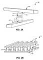
- FIG. 2Ais a simplified perspective view of a first embodiment of a memory cell provided in accordance with the present invention.
- FIG. 2Bis a simplified perspective view of a portion of a first memory level formed from a plurality of the memory cells of FIG. 2A .
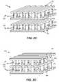
- FIG. 2Cis a simplified perspective view of a portion of a first exemplary three dimensional memory array provided in accordance with the present invention.
- FIG. 2Dis a simplified perspective view of a portion of a second exemplary three dimensional memory array provided in accordance with the present invention.
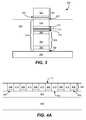
- FIG. 3is a cross-sectional view of an exemplary embodiment of the memory cell of FIG. 2A .
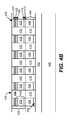
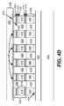
- FIGS. 4A-Dillustrate cross sectional views of a portion of a substrate during fabrication of a single memory level in accordance with the present invention.
- FIG. 5is a cross sectional view of a first alternative memory cell provided in accordance with the present invention.
- FIG. 6is a cross sectional view of a second alternative memory cell provided in accordance with the present invention.
- fabricating memory devices from rewriteable resistivity-switching materialsis difficult.
- many rewriteable resistivity-switching materialsare difficult to etch chemically, increasing fabrication costs and complexity associated with their use in integrated circuits.
- difficult-to-etch-chemically rewriteable resistivity-switching materialsmay be used within a memory cell without being etched.
- a memory cellis provided that includes a reversible resistivity-switching material formed using a selective deposition process so that the reversible resistivity-switching material may be used within the memory cell without being etched.
- a reversible resistance-switching elementmay be formed using nickel oxide as a reversible resistivity-switching material.
- Nickel oxide filmshave been shown to be suitable for use in memory cells, as described, for example, in the '939 Application, previously incorporated.
- Nickel-containing filmssuch as Ni, Ni x P y , NiO, NiO x , NiO x P y , etc., are difficult to etch chemically.
- a nickel oxide layermay be used in a reversible resistance-switching element of a memory cell without the nickel oxide layer being etched.
- a reversible resistance-switching elementmay be formed by employing a deposition process such as electroplating, electroless deposition, or the like, to selectively deposit a nickel-containing layer only on conductive surfaces formed above a substrate. In this manner, only the conductive surfaces on the substrate are patterned and/or etched (prior to deposition of the nickel-containing layer) and not the nickel-containing layer.
- a deposition processsuch as electroplating, electroless deposition, or the like
- nickel oxidemay be selectively deposited while in other embodiments, nickel may be selectively deposited and then oxidized to form nickel oxide. In either case, the need for etching of nickel and/or nickel oxide layers may be eliminated and memory cell fabrication significantly simplified.
- reversible or one-time-programmable resistivity-switching materialsfor use in memory cells.
- a layer of Nb, Ta, V, Al, Ti, Co, cobalt-nickel alloy, etc.may be selectively deposited, such as by electroplating, and oxidized to form a reversible resistivity-switching material.
- FIG. 1is a schematic illustration of an exemplary memory cell 100 provided in accordance with the present invention.
- the memory cell 100includes a reversible resistance-switching element 102 coupled to a steering element 104 .
- the reversible resistance-switching element 102includes a reversible resistivity-switching material (not separately shown) having a resistivity that may be reversibly switched between two or more states.
- the reversible resistivity-switching material of the element 102may be in an initial, low-resistivity state upon fabrication that is switchable to a high-resistivity state upon application of a first voltage and/or current. Application of a second voltage and/or current may return the reversible resistivity-switching material to a low-resistivity state.
- the reversible resistance-switching element 102may be in an initial, high-resistance state upon fabrication that is reversibly switchable to a low-resistance state upon application of the appropriate voltage (s) and/or current(s).
- one resistance stateWhen used in a memory cell, one resistance state may represent a binary “0” while another resistance state may represent a binary “1,” although more than two data/resistance states may be used.
- Numerous reversible resistivity-switching materials and operation of memory cells employing reversible resistance-switching elementsare described, for example, the '939 Application, previously incorporated.
- the reversible resistance-switching element 102is formed using a selective deposition process. As will be described further below, use of a selective deposition process allows a reversible resistivity-switching material to be provided within the reversible resistance-switching element 102 without the reversible resistivity-switching material having to be etched. Fabrication of the reversible resistance-switching element 102 thereby is simplified.
- the steering element 104may include a thin film transistor, a diode, or another suitable steering element that exhibits non-ohmic conduction by selectively limiting the voltage across and/or the current flow through the reversible resistance-switching element 102 .
- the memory cell 100may be used as part of a two or three dimensional memory array and data may be written to and/or read from the memory cell 100 without affecting the state of other memory cells in the array.
- Exemplary embodiments of the memory cell 100 , the reversible resistance-switching element 102 and the steering element 104are described below with reference to FIGS. 2A-6 .
- FIG. 2Ais a simplified perspective view of a first embodiment of a memory cell 200 provided in accordance with the present invention.
- the memory cell 200includes a reversible resistance-switching element 202 coupled in series with a diode 204 between a first conductor 206 and a second conductor 208 .
- a barrier layer 210 and/or a conductive layer 212may be formed between the reversible resistance-switching element 202 and the diode 204 .
- the barrier layer 210may include titanium nitride, tantalum nitride, tungsten nitride, etc.
- the conductive layer 212may include tungsten or another suitable metal layer.
- the barrier layer 210 and/or conductive layer 212may serve as a hard mask during formation of the diode 204 .
- Such a hard maskis described, for example, in U.S. patent application Ser. No. 11/444,936, filed May 13, 2006 (hereinafter “the '936 Application”), now U.S. Pat. No. 7,575,984, which is hereby incorporated by reference herein in its entirety.
- An additional barrier layer 213such as titanium nitride, tantalum nitride, tungsten nitride, etc., also may be formed between the diode 204 and the first conductor 206 .
- the reversible resistance-switching element 202is selectively formed so as to simplify fabrication of the memory cell 200 .
- the reversible resistance-switching element 202includes at least a portion of a nickel oxide layer formed by selectively depositing nickel and then oxidizing the nickel layer.
- Ni, Ni x P y or another similar form of nickelmay be selectively deposited using electroless deposition, electroplating or a similar selective process, and then oxidized to form nickel oxide (e.g., using rapid thermal oxidation or another oxidation process).
- nickel oxideitself may be selectively deposited.
- an NiO—, NiO x — or NiO x P y -containing layermay be selectively deposited above the diode 204 using a selective deposition process and then annealed and/or oxidized (if necessary).
- the reversible resistance-switching element 202is shown as being positioned above the diode 204 in FIG. 2A , it will be understood that in alternative embodiments, the reversible resistance-switching element 202 may be positioned below the diode 204 (as described below, for example, with reference to FIG. 6 ). In some embodiments, only a portion, such as one or more filaments, of the reversible resistance-switching element 202 may switch and/or be switchable.
- the diode 204may include any suitable diode such as a vertical polycrystalline p-n or p-i-n diode, whether upward pointing with an n-region above a p-region of the diode or downward pointing with a p-region above an n-region of the diode. Exemplary embodiments of the diode 204 are described below with reference to FIG. 3 .
- the first and/or second conductor 206 , 208may include any suitable conductive material such as tungsten, any appropriate metal, heavily doped semiconductor material, a conductive silicide, a conductive silicide-germanide, a conductive germanide, or the like.
- first and second conductors 206 , 208are rail-shaped and extend in different directions (e.g., substantially perpendicular to one another). Other conductor shapes and/or configurations may be used. In some embodiments, barrier layers, adhesion layers, antireflection coatings and/or the like (not shown) may be used with the first and/or second conductors 206 to improve device performance and/or aid in device fabrication.
- reversible resistance-switching element 202other materials may be used to form the reversible resistance-switching element 202 .
- materialssuch as Nb, Ta, V, Al, Ti, Co, cobalt-nickel alloy, etc., may be similarly selectively deposited over diode 204 (such as over the barrier layer 210 and/or over the conductive layer 212 as shown in FIG. 2A ) and, if necessary, oxidized and/or annealed to form the reversible resistance-switching element 202 .
- FIG. 2Bis a simplified perspective view of a portion of a first memory level 214 formed from a plurality of the memory cells 200 of FIG. 2A .
- the reversible resistance-switching element 202 , the diode 204 , the barrier layers 210 and 213 and the conductive layer 212are not separately shown.
- the memory array 214is a “cross-point” array including a plurality of bit lines (second conductors 208 ) and word lines (first conductors 206 ) to which multiple memory cells are coupled (as shown). Other memory array configurations may be used, as may multiple levels of memory.
- FIG. 2Cis a simplified perspective view of a portion of a monolithic three dimensional array 216 that includes a first memory level 218 positioned below a second memory level 220 .
- each memory level 218 , 220includes a plurality of memory cells 200 in a cross-point array.
- additional layerse.g., an interlevel dielectric
- FIG. 2Cmay be present between the first and second memory levels 218 and 220 , but are not shown in FIG. 2C for simplicity.
- all diodesmay “point” in the same direction, such as upward or downward depending on whether p-i-n diodes having a p-doped region on the bottom or top of the diode are employed, simplifying diode fabrication.
- the memory levelsmay be formed, as described, for example, in U.S. Pat. No. 6,952,030, “High-density three-dimensional memory cell,” which is hereby incorporated by reference herein in its entirety for all purposes.
- the upper conductors of a first memory levelmay be used as the lower conductors of a second memory level that is positioned above the first memory level as shown in FIG. 2D .
- the diodes on adjacent memory levelspreferably point in opposite directions as described in U.S. patent application Ser. No. 11/692,151, filed Mar. 27, 2007 (hereinafter “the '151 Application”), now U.S. Pat. No. 7,767,499, which is hereby incorporated by reference herein in its entirety for all purposes.
- the diodes of the first memory level 218may be upward pointing diodes as indicated by arrow A 1 (e.g., with p regions at the bottom of the diodes), while the diodes of the second memory level 220 may be downward pointing diodes as indicated by arrow A 2 (e.g., with n regions at the bottom of the diodes), or vice versa.
- a monolithic three dimensional memory arrayis one in which multiple memory levels are formed above a single substrate, such as a wafer, with no intervening substrates.
- the layers forming one memory levelare deposited or grown directly over the layers of an existing level or levels.
- stacked memorieshave been constructed by forming memory levels on separate substrates and adhering the memory levels atop each other, as in Leedy, U.S. Pat. No. 5,915,167, “Three dimensional structure memory.”
- the substratesmay be thinned or removed from the memory levels before bonding, but as the memory levels are initially formed over separate substrates, such memories are not true monolithic three dimensional memory arrays.
- FIG. 3is a cross-sectional view of an exemplary embodiment of the memory cell 200 of FIG. 2A .
- the memory cell 200includes the reversible resistance-switching element 202 , the diode 204 and the first and second conductors 206 , 208 .
- the diode 204may be a vertical p-n or p-i-n diode, which may either point upward or downward.
- adjacent memory levelspreferably have diodes that point in opposite directions such as downward-pointing p-i-n diodes for a first memory level and upward-pointing p-i-n diodes for an adjacent, second memory level (or vice versa).
- the diode 204may be formed from a polycrystalline semiconductor material such as polysilicon, a polycrystalline silicon-germanium alloy, polygermanium or any other suitable material.
- the diode 204may include a heavily doped n+ polysilicon region 302 , a lightly doped or an intrinsic (unintentionally doped) polysilicon region 304 above the n+ polysilicon region 302 and a heavily doped, p+ polysilicon region 306 above the intrinsic region 304 .
- a thin (e.g., a few hundred angstroms or less) germanium and/or silicon-germanium alloy layermay be formed on the n+ polysilicon region 302 to prevent and/or reduce dopant migration from the n+ polysilicon region 302 into the intrinsic region 304 , as described, for example, in U.S. patent application Ser. No. 11/298,331, filed Dec. 9, 2005 (hereinafter “the '331 Application”), now U.S. Pat. No. 7,405,465, which is hereby incorporated by reference herein in its entirety for all purposes.
- a barrier layer 308such as titanium nitride, tantalum nitride, tungsten nitride, etc., may be formed between the first conductor 206 and the n+ region 302 (e.g., to prevent and/or reduce migration of metal atoms into the polysilicon regions).
- a silicide layer 310may be formed on the diode 204 to place the deposited silicon in a low resistivity state, as fabricated.
- a low resistivity stateallows for easier programming of the memory cell 200 as a large voltage is not required to switch the deposited silicon to a low resistivity state.
- a silicide-forming metal layer 312such as titanium or cobalt may be deposited on the p+ polysilicon region 306 .
- a subsequent anneal step(described below) employed to crystallize the deposited silicon that forms the diode 204 , the silicide-forming metal layer 312 and the deposited silicon of the diode 204 interact to form the silicide layer 310 , consuming all or a portion of the silicide-forming metal layer 312 .
- silicide-forming materialssuch as titanium and/or cobalt react with deposited silicon during annealing to form a silicide layer.
- silicide layersmay serve as “crystallization templates” or “seeds” for adjacent deposited silicon as the deposited silicon crystallizes (e.g., the silicide layer 310 enhances the crystalline structure of the silicon diode 204 during annealing). Lower resistivity silicon thereby is provided. Similar results may be achieved for silicon-germanium alloy and/or germanium diodes.
- the reversible resistance-switching element 202is formed by a selective deposition process. In some embodiments, the reversible resistance-switching element 202 may be formed over the conductive silicide-forming metal layer 312 (or on a conductive barrier layer formed over the silicide-forming metal layer 312 ). (Such layers may be patterned during formation of the diode 204 as described below with reference to FIGS. 4A-4D .)
- a metal hard maskmay be formed over the silicide-forming metal layer 312 prior to formation of the resistance-switching element 202 .
- a barrier layer 314 and/or a conductive layer 316may be formed over the silicide-forming metal layer 312 .
- the barrier layer 314may include titanium nitride, tantalum nitride, tungsten nitride, etc., and the conductive layer 316 may include tungsten or another suitable metal layer.
- the barrier layer 314 and/or conductive layer 316may serve as a hard mask during formation of the diode 204 and may mitigate any overetching that may occur during formation of the top conductor 208 (as described in the '936 Application, previously incorporated).
- the barrier layer 314 and conductive layer 316may be patterned and etched, and then serve as a mask during etching of the diode 204 .
- Etching of the conductive layer 316 , barrier layer 314 , silicide-forming metal layer 312 , diode 204 (p+ polysilicon layer 306 , intrinsic layer 304 , n+ polysilicon layer 302 ) and barrier layer 308creates a pillar structure 318 .
- Dielectric material 320is deposited on top of and around the pillar structure 318 so as to isolate the pillar structure 318 from other similar pillar structures of other memory cells (not shown) fabricated on a memory level that includes the memory cell 200 .
- a CMP or dielectric etchback stepthen is performed to planarize the dielectric material 320 and remove the dielectric material from the top of the conductive layer 316 .
- the reversible resistance-switching element 202may be formed over the patterned and etched conductive layer 316 by a selective deposition process.
- a nickel oxide layermay be selectively formed over the patterned and etched conductive layer 316 by (1) selectively depositing nickel oxide, such as NiO, NiO x , NiO x P y and, if needed, annealing and/or oxidizing the nickel oxide; and/or (2) selectively depositing nickel and then oxidizing the nickel.
- nickel oxideonly deposits on the patterned and etched top surface of the conductive layer 316 , the need for etching of nickel and/or nickel oxide layers may be eliminated and memory cell fabrication significantly simplified. Further, any desired thickness of nickel oxide may be formed. In some embodiments, a nickel oxide layer thickness of about 1000 angstroms or less, and more preferably about 500 angstroms or less, is employed for the reversible resistance-switching element 202 (although other thickness ranges may be used).
- an electroless deposition processis employed to selectively deposit nickel or nickel oxide on the conductive layer 316 .
- an aqueous solutionmay be employed to selectively form nickel or nickel oxide on the conductive layer 316 by submerging the conductive layer 316 in the aqueous solution.
- the aqueous solutionmay include, for example, one or more dissolved salts/precursors, complexing agents and/or buffers for regulating pH of the solution.
- the aqueous solutionmay include nickel salts and/or nickel salt hydroxides, such as nickel sulfates, nickel sulfites, nickel phosphates, nickel phosphides, nickel hydroxides, ammonia phosphates, or mixtures of the same.
- Further exemplary componentsmay include NiSO 4 , NaH 2 PO 2 , sodium citrate, (NH 4 ) 2 SO 4 , or the like. It will be understood that either nickel or nickel oxide (or both) may be deposited on the conductive layer 316 depending on the exact components used to form the aqueous solution and/or other process conditions.
- Exemplary process conditionsinclude submerging the conductive layer 316 in an aqueous nickel-containing solution for about 1 second to about 5 minutes while the aqueous solution is maintained at a temperature of between about 20° C. to 85° C.
- Additional exemplary aqueous solutions and/or process conditions that may be used to selectively form a nickel or nickel oxide layerare described in N. Takano et al., “Mechanism of the Chemical Deposition of Nickel on Silicon Wafers in Aqueous Solution,” Journal of Electrochemical Society, 146(4) pp. 1407-1411 (1999), which is hereby incorporated by reference herein in its entirety for all purposes.
- deposited nickel or nickel oxidemay include Ni, Ni x P y , NiO, NiO x , NiO x P y , or other similar materials.
- a thermal oxidation processmay be used to either form nickel oxide from selectively deposited nickel or to improve the morphology and/or electrical characteristics of selectively deposited nickel oxide.
- Exemplary oxidation conditionsinclude rapid thermal oxidation in an oxygen environment such as O 2 for about 20 seconds to 10 minutes at a temperature of about 400° C. to 800° C. Other oxidation or annealing processes, oxygen species, times and/or temperatures may be used.
- Another suitable selective deposition process that may be used to form a nickel-containing layer on the patterned and etched conductive layer 316includes conventional nickel electroplating. Any suitable electroplating process may be employed to selectively deposit nickel on the conductive layer 316 . Thereafter, the electroplated nickel may be oxidized to form nickel oxide as described above.
- materialsmay be used to form the reversible resistance-switching element 202 .
- materialssuch as Nb, Ta, V, Al, Ti, Co, cobalt-nickel alloy, etc., may be similarly selectively deposited over diode 204 (such as over the barrier layer 210 and/or over the conductive layer 212 as shown in FIG. 2A ) and annealed and/or oxidized, if necessary.
- the top conductor 208is formed.
- one or more barrier layers and/or adhesion layers 322may be formed over the reversible resistance-switching element 202 prior to deposition of a conductive layer 324 .
- the conductive layer 324 and barrier layer 322may be patterned and/or etched together to form the top conductor 208 .
- the top conductor 208may be formed using a damascene process as described below with reference to FIGS. 4A-4D .
- the memory cell 200may be annealed to crystallize the deposited semiconductor material of the diode 204 (and/or to form the silicide layer 310 ).
- the annealmay be performed for about 10 seconds to about 2 minutes in nitrogen at a temperature of about 600° C. to 800° C., and more preferably between about 650° C. and 750° C. Other annealing times, temperatures and/or environments may be used.
- the silicide layer 310may serve as a “crystallization template” or “seed” during annealing for underlying deposited semiconductor material that forms the diode 204 . Lower resistivity diode material thereby is provided.
- FIGS. 4A-DAn exemplary process for fabricating a memory cell in accordance with the present invention is described below with reference to FIGS. 4A-D .
- FIGS. 4A-Dillustrate cross sectional views of a portion of a substrate 400 during fabrication of a first memory level in accordance with the present invention.
- the first memory levelincludes a plurality of memory cells that each include a reversible resistance-switching element formed using a selective deposition process. Additional memory levels may be fabricated above the first memory level (as described previously with reference to FIGS. 2C-2D ).
- the substrate 400is shown as having already undergone several processing steps.
- the substrate 400may be any suitable substrate such as a silicon, germanium, silicon-germanium, undoped, doped, bulk, silicon-on-insulator (SOI) or other substrate with or without additional circuitry.
- the substrate 400may include one or more n-well or p-well regions (not shown).
- Isolation layer 402is formed above the substrate 400 .
- the isolation layer 402may be a layer of silicon dioxide, silicon nitride, silicon oxynitride or any other suitable insulating layer.
- an adhesion layer 404is formed over the isolation layer 402 (e.g., by physical vapor deposition or another method).
- the adhesion layer 404may be about 20 to about 500 angstroms, and preferably about 100 angstroms, of titanium nitride or another suitable adhesion layer such as tantalum nitride, tungsten nitride, combinations of one or more adhesion layers, or the like. Other adhesion layer materials and/or thicknesses may be employed.
- the adhesion layer 404may be optional.
- the conductive layer 406may include any suitable conductive material such as tungsten or another appropriate metal, heavily doped semiconductor material, a conductive silicide, a conductive silicide-germanide, a conductive germanide, or the like deposited by any suitable method (e.g., chemical vapor deposition (CVD), physical vapor deposition (PVD), etc.). In at least one embodiment, the conductive layer 406 may comprise about 200 to about 2500 angstroms of tungsten. Other conductive layer materials and/or thicknesses may be used.
- CVDchemical vapor deposition
- PVDphysical vapor deposition
- the adhesion layer 404 and the conductive layer 406are patterned and etched.
- the adhesion layer 404 and the conductive layer 406may be patterned and etched using conventional lithography techniques, with a soft or hard mask, and wet or dry etch processing.
- the adhesion layer 404 and conductive layer 406are patterned and etched so as to form substantially parallel, substantially co-planar conductors 408 (as shown in FIG. 4A ).
- Exemplary widths for the conductors 408 and/or spacings between the conductors 408range from about 200 to about 2500 angstroms, although other conductor widths and/or spacings may be used.
- a dielectric layer 410is formed over the substrate 400 so as to fill the voids between the conductors 408 .
- a dielectric layer 410may be deposited on the substrate 400 and planarized using chemical mechanical polishing or an etchback process to form a planar surface 412 .
- the planar surface 412includes exposed top surfaces of the conductors 408 separated by dielectric material (as shown).
- dielectric materialsuch as silicon nitride, silicon oxynitride, low K dielectrics, etc., and/or other dielectric layer thicknesses may be used.
- Exemplary low K dielectricsinclude carbon doped oxides, silicon carbon layers, or the like.
- the conductors 408may be formed using a damascene process in which the dielectric layer 410 is formed and patterned to create openings or voids for the conductors 408 .
- the openings or voidsthen may be filled with the adhesion layer 404 and the conductive layer 406 (and/or a conductive seed, conductive fill and/or barrier layer if needed).
- the adhesion layer 404 and conductive layer 406then may be planarized to form the planar surface 412 . In such an embodiment, the adhesion layer 404 will line the bottom and sidewalls of each opening or void.
- a barrier layer 414is formed over the planarized top surface 412 of the substrate 400 .
- the barrier layer 414may be about 20 to about 500 angstroms, and preferably about 100 angstroms, of titanium nitride or another suitable barrier layer such as tantalum nitride, tungsten nitride, combinations of one or more barrier layers, barrier layers in combination with other layers such as titanium/titanium nitride, tantalum/tantalum nitride or tungsten/tungsten nitride stacks, or the like. Other barrier layer materials and/or thicknesses may be employed.
- each diodemay be a vertical p-n or p-i-n diode as previously described.
- each diodeis formed from a polycrystalline semiconductor material such as polysilicon, a polycrystalline silicon-germanium alloy, polygermanium or any other suitable material. For convenience, formation of a polysilicon, downward-pointing diode is described herein. It will be understood that other materials and/or diode configurations may be used.
- n+ silicon layer 416is deposited on the barrier layer 414 .
- the n+ silicon layer 416is in an amorphous state as deposited.
- the n+ silicon layer 416is in a polycrystalline state as deposited. CVD or another suitable process may be employed to deposit the n+ silicon layer 416 .
- the n+ silicon layer 416may be formed, for example, from about 100 to about 1000 angstroms, preferably about 100 angstroms, of phosphorus or arsenic doped silicon having a doping concentration of about 10 21 cm-3. Other layer thicknesses, doping types and/or doping concentrations may be used.
- the n+ silicon layer 416may be doped in situ, for example, by flowing a donor gas during deposition. Other doping methods may be used (e.g., implantation).
- a lightly doped, intrinsic and/or unintentionally doped silicon layer 418is formed over the n+ silicon layer 416 .
- the intrinsic silicon layer 418is in an amorphous state as deposited. In other embodiments, the intrinsic silicon layer 418 is in a polycrystalline state as deposited. CVD or another suitable deposition method may be employed to deposit the intrinsic silicon layer 418 .
- the intrinsic silicon layer 418may be about 500 to about 4800 angstroms, preferably about 2500 angstroms, in thickness. Other intrinsic layer thicknesses may be used.
- a thin (e.g., a few hundred angstroms or less) germanium and/or silicon-germanium alloy layermay be formed on the n+ silicon layer 416 prior to deposition of the intrinsic silicon layer 418 to prevent and/or reduce dopant migration from the n+ silicon layer 416 into the intrinsic silicon layer 418 (as described in the '331 Application, previously incorporated).
- Heavily doped, p-type siliconis either deposited and doped by ion implantation or is doped in situ during deposition to form a p+ silicon layer 420 .
- a blanket p+ implantmay be employed to implant boron a predetermined depth within the intrinsic silicon layer 418 .
- Exemplary implantable molecular ionsinclude BF 2 , BF 3 , B and the like.
- an implant dose of about 1-5 ⁇ 10 15 ions/cm 2may be employed.
- Other implant species and/or dosesmay be used.
- a diffusion processmay be employed.
- the resultant p+ silicon layer 420has a thickness of about 100-700 angstroms, although other p+ silicon layer sizes may be used.
- a silicide-forming metal layer 422is deposited over the p+ silicon layer 420 .
- exemplary silicide-forming metalsinclude sputter or otherwise deposited titanium or cobalt.
- the silicide-forming metal layer 422has a thickness of about 10 to about 200 angstroms, preferably about 20 to about 50 angstroms and more preferably about 20 angstroms. Other silicide-forming metal layer materials and/or thicknesses may be used.
- a barrier layer 424is deposited over the silicide-forming metal layer 422 .
- the barrier layer 424may be about 20 to about 500 angstroms, and preferably about 100 angstroms, of titanium nitride or another suitable barrier layer such as tantalum nitride, tungsten nitride, combinations of one or more barrier layers, barrier layers in combination with other layers such as titanium/titanium nitride, tantalum/tantalum nitride or tungsten/tungsten nitride stacks, or the like. Other barrier layer materials and/or thicknesses may be employed.
- a conductive layer 426is formed over the barrier layer 424 .
- the conductive layer 426may be about 50 to about 1000 angstroms, and preferably about 500 angstroms of conductive material such as tungsten or another suitable metal.
- barrier layer 414 , silicon regions 416 , 418 , and 420 , silicide-forming metal layer 422 , barrier layer 424 and conductive layer 426are then patterned and etched into pillars 428 .
- the conductive layer 426 and barrier layer 424are etched. The etch continues, etching silicide-forming metal layer 422 , silicon regions 420 , 418 , and 416 and barrier layer 414 .
- Conductive layer 426 and barrier layer 414serve as a hard mask during the silicon etch.
- a hard maskis an etched layer which serves to pattern the etch of an underlying layer; if all of the photoresist present on the conductive layer 426 has been consumed, the hard mask can provide the pattern in its stead.
- the pillars 428are formed in a single photolithographic step. Conventional lithography techniques, and wet or dry etch processing may be employed to form the pillars 428 .
- Each pillar 428includes a p-i-n, downward-pointing diode 430 . Upward-pointing p-i-n diodes may be similarly formed.
- a dielectric layer 432is deposited over the pillars 428 to fill the voids between the pillars 428 .
- a dielectric layer 432is deposited over the pillars 428 to fill the voids between the pillars 428 .
- approximately 200-7000 angstroms of silicon dioxidemay be deposited and planarized using chemical mechanical polishing or an etchback process to form a planar surface 434 .
- the planar surface 434includes exposed top surfaces of the pillars 428 separated by dielectric material 432 (as shown).
- Other dielectric materialssuch as silicon nitride, silicon oxynitride, low K dielectrics, etc., and/or other dielectric layer thicknesses may be used.
- Exemplary low K dielectricsinclude carbon doped oxides, silicon carbon layers, or the like.
- a reversible resistance-switching element 436( FIG. 4C ) is selectively formed over each pillar 428 .
- a nickel oxide layermay be selectively formed over each conductive pillar 428 by selectively depositing (1) nickel oxide; and/or (2) selectively depositing nickel and then oxidizing the nickel. In either case, the need for etching of nickel and/or nickel oxide layers may be eliminated and memory cell fabrication significantly simplified.
- any suitable method for selectively depositing nickel or a nickel oxidemay be used such as electroless deposition, electroplating or the like.
- the reversible resistance-switching element 436 formed over each conductive pillar 428includes a nickel oxide layer having a thickness of about 1000 angstroms or less, and more preferably a thickness of about 500 angstroms or less. Other nickel oxide thicknesses may be employed.
- the nickel oxide layermay include, for example, NiO, NiO x , and NiO x P y , or other similar materials. Other materials such as Nb, Ta, V, Al, Ti, Co, cobalt-nickel alloy, etc., may be similarly selectively deposited, oxidized and/or annealed to form a selectively deposited, reversible resistance-switching element over each pillar 428 .
- a second set of conductors 438may be formed above the pillars 428 in a manner similar to the formation of the bottom set of conductors 408 .
- one or more barrier layers and/or adhesion layers 440may be deposited over the reversible resistance-switching elements 436 prior to deposition of a conductive layer 442 used to form the upper, second set of conductors 438 .
- the conductive layer 442may be formed from any suitable conductive material such as tungsten, another suitable metal, heavily doped semiconductor material, a conductive silicide, a conductive silicide-germanide, a conductive germanide, or the like deposited by any suitable method (e.g., CVD, PVD, etc.). Other conductive layer materials may be used.
- suitable conductive materialsuch as tungsten, another suitable metal, heavily doped semiconductor material, a conductive silicide, a conductive silicide-germanide, a conductive germanide, or the like deposited by any suitable method (e.g., CVD, PVD, etc.). Other conductive layer materials may be used.
- Barrier layers and/or adhesion layers 440may include titanium nitride or another suitable layer such as tantalum nitride, tungsten nitride, combinations of one or more layers, or any other suitable material(s).
- the deposited conductive layer 442 and barrier and/or adhesion layer 440may be patterned and etched to form the second set of conductors 438 .
- the upper conductors 438are substantially parallel, substantially coplanar conductors that extend in a different direction than the lower conductors 408 .
- the upper conductors 438may be formed using a damascene process in which a dielectric layer is formed and patterned to create openings or voids for the conductors 438 .
- the conductive layer 426 and barrier layer 424may mitigate the effects of overetching of such a dielectric layer during formation of the openings or voids for the upper conductors 438 , preventing accidental shorting of the diodes 430 .
- the openings or voidsmay be filled with the adhesion layer 440 and the conductive layer 442 (and/or a conductive seed, conductive fill and/or barrier layer if needed).
- the adhesion layer 440 and conductive layer 442then may be planarized to form a planar surface.
- the structuremay be annealed to crystallize the deposited semiconductor material of the diodes 430 (and/or to form silicide regions by reaction of the silicide-forming metal layer 422 with p+ region 420 ).
- the annealmay be performed for about 10 seconds to about 2 minutes in nitrogen at a temperature of about 600° C. to 800° C., and more preferably between about 650° C. and 750° C. Other annealing times, temperatures and/or environments may be used.
- the silicide regions formed as each silicide-forming metal layer region 422 and p+ region 420 reactmay serve as “crystallization templates” or “seeds” during annealing for underlying deposited semiconductor material that forms the diodes 430 (e.g., changing any amorphous semiconductor material to polycrystalline semiconductor material and/or improving overall crystalline properties of the diodes 430 ). Lower resistivity diode material thereby is provided.
- FIG. 5is a cross sectional view of an exemplary memory cell 500 provided in accordance with the present invention.
- the memory cell 500includes a thin film transistor (TFT), such as a thin film, metal oxide semiconductor field effect transistor (MOSFET) 502 coupled to a reversible resistance-switching element 504 formed above a substrate 505 .
- TFTthin film transistor
- MOSFETmetal oxide semiconductor field effect transistor
- the MOSFET 502may be an n-channel or a p-channel thin film MOSFET formed on any suitable substrate.
- an insulating region 506such as silicon dioxide, silicon nitride, oxynitride, etc., is formed above the substrate 505 and a deposited semiconductor region 507 such as deposited silicon, germanium, silicon-germanium, etc., is formed above the insulating region 506 .
- the thin film MOSFET 502is formed within the deposited semiconductor region 507 and is insulated from the substrate 505 by the insulating region 506 .
- the MOSFET 502includes source/drain regions 508 , 510 and channel region 512 , as well as gate dielectric layer 514 , gate electrode 516 and spacers 518 a - b .
- the source/drain regions 508 , 510may be doped p-type and the channel region 512 may be doped n-type, while in other embodiments the source/drain regions 508 , 510 may be doped n-type and the channel region 512 may be doped p-type.
- the MOSFET 502may be electrically isolated by isolation regions (not shown) formed using an STI, LOCOS or other similar process.
- gate, source and/or drain regions of the MOSFET 502may be shared with other transistors (not shown) formed on the substrate 505 .
- the reversible resistance-switching element 504includes a reversible resistivity-switching material 522 formed over a conductive plug 526 .
- the reversible resistivity-switching material 522is formed using a selective deposition process as previously described with reference to the embodiments of FIGS. 1-4D .
- a nickel oxide layermay be selectively formed over the conductive plug 526 by selectively depositing (1) nickel oxide; and/or (2) selectively deposited nickel and then oxidizing the nickel.
- Exemplary selective deposition processesinclude electroless deposition, electroplating, or the like.
- Other materialsmay be selectively deposited, oxidized and/or annealed in accordance with the present invention to form reversible resistivity-switching materials for use in memory cell 500 (e.g., Nb, Ta, V, Al, Ti, Co, cobalt-nickel alloy, etc.).
- the reversible resistance-switching element 504is coupled to the source/drain region 510 of the MOSFET 502 by the first conductive plug 526 and to a first metal level (M 1 ) line 528 by a second conductive plug 530 (which extend through a dielectric layer 532 ).
- a third conductive plug 534couples the source/drain region 508 of the MOSFET 502 to an M 1 line 536 .
- the conductive plugs and/or linesmay be formed from any suitable materials (without or without barriers layers) such as tungsten, another metal, heavily doped semiconductor material, a conductive silicide, a conductive silicide-germanide, a conductive germanide, or the like.
- the dielectric layer 532may include any suitable dielectric such as silicon dioxide, silicon nitride, silicon oxynitride, low K dielectrics, etc.
- the thin film MOSFET 502operates as a steering element in a manner similar to that of the diodes employed in the memory cells of FIGS. 2A-4D , selectively limiting the voltage applied across and/or the current flow through the reversible resistance-switching element 504 .
- the reversible resistance-switching element 504includes a nickel oxide layer having a thickness of about 1000 angstroms or less, and more preferably a thickness of about 500 angstroms or less. Other nickel oxide thicknesses may be employed.
- FIG. 6is a cross sectional view of an exemplary memory cell 600 provided in accordance with the present invention.
- the memory cell 600is similar to the memory cell 200 of FIG. 3 , with the exception that the reversible resistance-switching element 202 is formed below the diode 204 .
- the reversible resistance-switching element 202is formed by selectively depositing a conductive material 602 on the patterned and etched bottom conductor 206 .
- the conductive material 602then may be annealed and/or oxidized if necessary, in accordance with the present invention, to form a reversible resistivity-switching material 604 for use in memory cell 600 .
- the conductive material 602may include a layer of Ni, Ni x P y , NiO, NiO x , NiO x P y , Nb, Ta, V, Al, Ti, Co, cobalt-nickel alloy, etc., selectively deposited, such as by electroplating, and oxidized to form the reversible resistivity-switching material layer 604 .
- a portion of the reversible resistivity-switching material layer 604 that vertically overlaps and/or aligns with the diode 204may serve as the reversible resistance-switching element 202 between the diode 204 and the first conductor 206 of the memory cell 600 .
- only a portion, such as one or more filaments, of the reversible resistance-switching element 202may switch and/or be switchable. Because the layer 604 is selectively deposited on the already patterned and etched bottom conductor 206 , the reversible resistivity-switching material layer 604 does not require etching.
- the present inventionhas been described primarily with regard to selective deposition of nickel and nickel oxide, it will be understood that other materials may be selectively deposited for use in a reversible resistance-switching element such as Ta, Nb, Al, V, Co, cobalt-nickel alloy, Ti, etc., forming, for example, Ta 2 O 5 , Nb 2 O 5 , Al 2 O 3 , V 2 O 5 , CoO, (Co x Ni y )O z , and TiO 2 .
- a reversible resistance-switching elementsuch as Ta, Nb, Al, V, Co, cobalt-nickel alloy, Ti, etc.
Landscapes
- Semiconductor Memories (AREA)
Abstract
Description
Claims (20)
Priority Applications (1)
| Application Number | Priority Date | Filing Date | Title |
|---|---|---|---|
| US13/556,312US8913417B2 (en) | 2007-06-29 | 2012-07-24 | Memory cell that employs a selectively deposited reversible resistance-switching element and methods of forming the same |
Applications Claiming Priority (2)
| Application Number | Priority Date | Filing Date | Title |
|---|---|---|---|
| US11/772,084US8233308B2 (en) | 2007-06-29 | 2007-06-29 | Memory cell that employs a selectively deposited reversible resistance-switching element and methods of forming the same |
| US13/556,312US8913417B2 (en) | 2007-06-29 | 2012-07-24 | Memory cell that employs a selectively deposited reversible resistance-switching element and methods of forming the same |
Related Parent Applications (1)
| Application Number | Title | Priority Date | Filing Date |
|---|---|---|---|
| US11/772,084ContinuationUS8233308B2 (en) | 2007-06-29 | 2007-06-29 | Memory cell that employs a selectively deposited reversible resistance-switching element and methods of forming the same |
Publications (2)
| Publication Number | Publication Date |
|---|---|
| US20120286233A1 US20120286233A1 (en) | 2012-11-15 |
| US8913417B2true US8913417B2 (en) | 2014-12-16 |
Family
ID=40159269
Family Applications (2)
| Application Number | Title | Priority Date | Filing Date |
|---|---|---|---|
| US11/772,084Expired - Fee RelatedUS8233308B2 (en) | 2007-06-29 | 2007-06-29 | Memory cell that employs a selectively deposited reversible resistance-switching element and methods of forming the same |
| US13/556,312Active2028-05-19US8913417B2 (en) | 2007-06-29 | 2012-07-24 | Memory cell that employs a selectively deposited reversible resistance-switching element and methods of forming the same |
Family Applications Before (1)
| Application Number | Title | Priority Date | Filing Date |
|---|---|---|---|
| US11/772,084Expired - Fee RelatedUS8233308B2 (en) | 2007-06-29 | 2007-06-29 | Memory cell that employs a selectively deposited reversible resistance-switching element and methods of forming the same |
Country Status (1)
| Country | Link |
|---|---|
| US (2) | US8233308B2 (en) |
Cited By (1)
| Publication number | Priority date | Publication date | Assignee | Title |
|---|---|---|---|---|
| US9748311B2 (en) | 2014-11-07 | 2017-08-29 | Micron Technology, Inc. | Cross-point memory and methods for fabrication of same |
Families Citing this family (110)
| Publication number | Priority date | Publication date | Assignee | Title |
|---|---|---|---|---|
| US7812404B2 (en)* | 2005-05-09 | 2010-10-12 | Sandisk 3D Llc | Nonvolatile memory cell comprising a diode and a resistance-switching material |
| US7834338B2 (en)* | 2005-11-23 | 2010-11-16 | Sandisk 3D Llc | Memory cell comprising nickel-cobalt oxide switching element |
| US7816659B2 (en) | 2005-11-23 | 2010-10-19 | Sandisk 3D Llc | Devices having reversible resistivity-switching metal oxide or nitride layer with added metal |
| US7875871B2 (en)* | 2006-03-31 | 2011-01-25 | Sandisk 3D Llc | Heterojunction device comprising a semiconductor and a resistivity-switching oxide or nitride |
| US7829875B2 (en) | 2006-03-31 | 2010-11-09 | Sandisk 3D Llc | Nonvolatile rewritable memory cell comprising a resistivity-switching oxide or nitride and an antifuse |
| US7808810B2 (en)* | 2006-03-31 | 2010-10-05 | Sandisk 3D Llc | Multilevel nonvolatile memory cell comprising a resistivity-switching oxide or nitride and an antifuse |
| US8987702B2 (en) | 2007-05-01 | 2015-03-24 | Micron Technology, Inc. | Selectively conducting devices, diode constructions, constructions, and diode forming methods |
| US8233308B2 (en) | 2007-06-29 | 2012-07-31 | Sandisk 3D Llc | Memory cell that employs a selectively deposited reversible resistance-switching element and methods of forming the same |
| US7846785B2 (en)* | 2007-06-29 | 2010-12-07 | Sandisk 3D Llc | Memory cell that employs a selectively deposited reversible resistance-switching element and methods of forming the same |
| US7824956B2 (en) | 2007-06-29 | 2010-11-02 | Sandisk 3D Llc | Memory cell that employs a selectively grown reversible resistance-switching element and methods of forming the same |
| US7902537B2 (en) | 2007-06-29 | 2011-03-08 | Sandisk 3D Llc | Memory cell that employs a selectively grown reversible resistance-switching element and methods of forming the same |
| US7777215B2 (en)* | 2007-07-20 | 2010-08-17 | Macronix International Co., Ltd. | Resistive memory structure with buffer layer |
| US8558220B2 (en)* | 2007-12-31 | 2013-10-15 | Sandisk 3D Llc | Memory cell that employs a selectively fabricated carbon nano-tube reversible resistance-switching element formed over a bottom conductor and methods of forming the same |
| US8878235B2 (en) | 2007-12-31 | 2014-11-04 | Sandisk 3D Llc | Memory cell that employs a selectively fabricated carbon nano-tube reversible resistance-switching element and methods of forming the same |
| US8236623B2 (en)* | 2007-12-31 | 2012-08-07 | Sandisk 3D Llc | Memory cell that employs a selectively fabricated carbon nano-tube reversible resistance-switching element and methods of forming the same |
| US8530318B2 (en)* | 2008-04-11 | 2013-09-10 | Sandisk 3D Llc | Memory cell that employs a selectively fabricated carbon nano-tube reversible resistance-switching element formed over a bottom conductor and methods of forming the same |
| US8304284B2 (en)* | 2008-04-11 | 2012-11-06 | Sandisk 3D Llc | Memory cell that employs a selectively fabricated carbon nano-tube reversible resistance-switching element, and methods of forming the same |
| US8120951B2 (en) | 2008-05-22 | 2012-02-21 | Micron Technology, Inc. | Memory devices, memory device constructions, constructions, memory device forming methods, current conducting devices, and memory cell programming methods |
| US7920407B2 (en)* | 2008-10-06 | 2011-04-05 | Sandisk 3D, Llc | Set and reset detection circuits for reversible resistance switching memory material |
| US8270199B2 (en) | 2009-04-03 | 2012-09-18 | Sandisk 3D Llc | Cross point non-volatile memory cell |
| US7978498B2 (en) | 2009-04-03 | 2011-07-12 | Sandisk 3D, Llc | Programming non-volatile storage element using current from other element |
| US8279650B2 (en) | 2009-04-20 | 2012-10-02 | Sandisk 3D Llc | Memory system with data line switching scheme |
| EP2259267B1 (en)* | 2009-06-02 | 2013-08-21 | Imec | Method for manufacturing a resistive switching memory cell comprising a nickel oxide layer operable at low-power and memory cells obtained thereof |
| US8154904B2 (en) | 2009-06-19 | 2012-04-10 | Sandisk 3D Llc | Programming reversible resistance switching elements |
| US8207064B2 (en) | 2009-09-17 | 2012-06-26 | Sandisk 3D Llc | 3D polysilicon diode with low contact resistance and method for forming same |
| WO2011047151A2 (en) | 2009-10-14 | 2011-04-21 | Skeletal Dynamics Llc | Internal joint stabilizer for a multi-axis joint, such as a carpo-metacarpal joint or the like, and method of use |
| US8274130B2 (en) | 2009-10-20 | 2012-09-25 | Sandisk 3D Llc | Punch-through diode steering element |
| US8213243B2 (en) | 2009-12-15 | 2012-07-03 | Sandisk 3D Llc | Program cycle skip |
| US8223525B2 (en) | 2009-12-15 | 2012-07-17 | Sandisk 3D Llc | Page register outside array and sense amplifier interface |
| US8624293B2 (en) | 2009-12-16 | 2014-01-07 | Sandisk 3D Llc | Carbon/tunneling-barrier/carbon diode |
| KR20130001725A (en) | 2010-02-18 | 2013-01-04 | 쌘디스크 3디 엘엘씨 | Step soft program for reversible resistivity-switching elements |
| US8686419B2 (en) | 2010-02-23 | 2014-04-01 | Sandisk 3D Llc | Structure and fabrication method for resistance-change memory cell in 3-D memory |
| JP2011199197A (en)* | 2010-03-23 | 2011-10-06 | Toshiba Corp | Semiconductor memory device |
| US8385102B2 (en) | 2010-05-11 | 2013-02-26 | Sandisk 3D Llc | Alternating bipolar forming voltage for resistivity-switching elements |
| US9012307B2 (en)* | 2010-07-13 | 2015-04-21 | Crossbar, Inc. | Two terminal resistive switching device structure and method of fabricating |
| US8946046B1 (en) | 2012-05-02 | 2015-02-03 | Crossbar, Inc. | Guided path for forming a conductive filament in RRAM |
| US9570678B1 (en) | 2010-06-08 | 2017-02-14 | Crossbar, Inc. | Resistive RAM with preferental filament formation region and methods |
| US9601692B1 (en) | 2010-07-13 | 2017-03-21 | Crossbar, Inc. | Hetero-switching layer in a RRAM device and method |
| US8441835B2 (en) | 2010-06-11 | 2013-05-14 | Crossbar, Inc. | Interface control for improved switching in RRAM |
| CN103081093B (en) | 2010-06-11 | 2015-06-03 | 科洛斯巴股份有限公司 | Pillar structure and method of memory device |
| US8520425B2 (en) | 2010-06-18 | 2013-08-27 | Sandisk 3D Llc | Resistive random access memory with low current operation |
| US8724369B2 (en) | 2010-06-18 | 2014-05-13 | Sandisk 3D Llc | Composition of memory cell with resistance-switching layers |
| US8395926B2 (en) | 2010-06-18 | 2013-03-12 | Sandisk 3D Llc | Memory cell with resistance-switching layers and lateral arrangement |
| US8374018B2 (en) | 2010-07-09 | 2013-02-12 | Crossbar, Inc. | Resistive memory using SiGe material |
| US8947908B2 (en) | 2010-11-04 | 2015-02-03 | Crossbar, Inc. | Hetero-switching layer in a RRAM device and method |
| US8467227B1 (en) | 2010-11-04 | 2013-06-18 | Crossbar, Inc. | Hetero resistive switching material layer in RRAM device and method |
| US8569172B1 (en) | 2012-08-14 | 2013-10-29 | Crossbar, Inc. | Noble metal/non-noble metal electrode for RRAM applications |
| US8168506B2 (en) | 2010-07-13 | 2012-05-01 | Crossbar, Inc. | On/off ratio for non-volatile memory device and method |
| US8884261B2 (en) | 2010-08-23 | 2014-11-11 | Crossbar, Inc. | Device switching using layered device structure |
| US8492195B2 (en) | 2010-08-23 | 2013-07-23 | Crossbar, Inc. | Method for forming stackable non-volatile resistive switching memory devices |
| US9401475B1 (en) | 2010-08-23 | 2016-07-26 | Crossbar, Inc. | Method for silver deposition for a non-volatile memory device |
| US8889521B1 (en) | 2012-09-14 | 2014-11-18 | Crossbar, Inc. | Method for silver deposition for a non-volatile memory device |
| US8558212B2 (en) | 2010-09-29 | 2013-10-15 | Crossbar, Inc. | Conductive path in switching material in a resistive random access memory device and control |
| US8391049B2 (en) | 2010-09-29 | 2013-03-05 | Crossbar, Inc. | Resistor structure for a non-volatile memory device and method |
| USRE46335E1 (en) | 2010-11-04 | 2017-03-07 | Crossbar, Inc. | Switching device having a non-linear element |
| US8502185B2 (en) | 2011-05-31 | 2013-08-06 | Crossbar, Inc. | Switching device having a non-linear element |
| US8088688B1 (en) | 2010-11-05 | 2012-01-03 | Crossbar, Inc. | p+ polysilicon material on aluminum for non-volatile memory device and method |
| US8355271B2 (en) | 2010-11-17 | 2013-01-15 | Sandisk 3D Llc | Memory system with reversible resistivity-switching using pulses of alternate polarity |
| US8462580B2 (en) | 2010-11-17 | 2013-06-11 | Sandisk 3D Llc | Memory system with reversible resistivity-switching using pulses of alternatrie polarity |
| US8930174B2 (en) | 2010-12-28 | 2015-01-06 | Crossbar, Inc. | Modeling technique for resistive random access memory (RRAM) cells |
| US9153623B1 (en) | 2010-12-31 | 2015-10-06 | Crossbar, Inc. | Thin film transistor steering element for a non-volatile memory device |
| US8791010B1 (en) | 2010-12-31 | 2014-07-29 | Crossbar, Inc. | Silver interconnects for stacked non-volatile memory device and method |
| US8815696B1 (en) | 2010-12-31 | 2014-08-26 | Crossbar, Inc. | Disturb-resistant non-volatile memory device using via-fill and etchback technique |
| US8374051B2 (en) | 2011-03-03 | 2013-02-12 | Sandisk 3D Llc | Three dimensional memory system with column pipeline |
| US8553476B2 (en) | 2011-03-03 | 2013-10-08 | Sandisk 3D Llc | Three dimensional memory system with page of data across word lines |
| US9053766B2 (en) | 2011-03-03 | 2015-06-09 | Sandisk 3D, Llc | Three dimensional memory system with intelligent select circuit |
| US8699293B2 (en) | 2011-04-27 | 2014-04-15 | Sandisk 3D Llc | Non-volatile storage system with dual block programming |
| US8450710B2 (en) | 2011-05-27 | 2013-05-28 | Crossbar, Inc. | Low temperature p+ silicon junction material for a non-volatile memory device |
| US8394670B2 (en)* | 2011-05-31 | 2013-03-12 | Crossbar, Inc. | Vertical diodes for non-volatile memory device |
| US9620206B2 (en) | 2011-05-31 | 2017-04-11 | Crossbar, Inc. | Memory array architecture with two-terminal memory cells |
| US8619459B1 (en) | 2011-06-23 | 2013-12-31 | Crossbar, Inc. | High operating speed resistive random access memory |
| US9627443B2 (en) | 2011-06-30 | 2017-04-18 | Crossbar, Inc. | Three-dimensional oblique two-terminal memory with enhanced electric field |
| US9564587B1 (en) | 2011-06-30 | 2017-02-07 | Crossbar, Inc. | Three-dimensional two-terminal memory with enhanced electric field and segmented interconnects |
| US8946669B1 (en) | 2012-04-05 | 2015-02-03 | Crossbar, Inc. | Resistive memory device and fabrication methods |
| US8659929B2 (en) | 2011-06-30 | 2014-02-25 | Crossbar, Inc. | Amorphous silicon RRAM with non-linear device and operation |
| US9166163B2 (en) | 2011-06-30 | 2015-10-20 | Crossbar, Inc. | Sub-oxide interface layer for two-terminal memory |
| US9252191B2 (en) | 2011-07-22 | 2016-02-02 | Crossbar, Inc. | Seed layer for a p+ silicon germanium material for a non-volatile memory device and method |
| US8674724B2 (en) | 2011-07-29 | 2014-03-18 | Crossbar, Inc. | Field programmable gate array utilizing two-terminal non-volatile memory |
| US9729155B2 (en) | 2011-07-29 | 2017-08-08 | Crossbar, Inc. | Field programmable gate array utilizing two-terminal non-volatile memory |
| US10056907B1 (en) | 2011-07-29 | 2018-08-21 | Crossbar, Inc. | Field programmable gate array utilizing two-terminal non-volatile memory |
| JP2013069922A (en) | 2011-09-22 | 2013-04-18 | Toshiba Corp | Manufacturing method of nonvolatile semiconductor storage device and nonvolatile semiconductor storage device |
| US8716098B1 (en) | 2012-03-09 | 2014-05-06 | Crossbar, Inc. | Selective removal method and structure of silver in resistive switching device for a non-volatile memory device |
| JP5606478B2 (en)* | 2012-03-22 | 2014-10-15 | 株式会社東芝 | Semiconductor memory device |
| US9087576B1 (en) | 2012-03-29 | 2015-07-21 | Crossbar, Inc. | Low temperature fabrication method for a three-dimensional memory device and structure |
| US9685608B2 (en) | 2012-04-13 | 2017-06-20 | Crossbar, Inc. | Reduced diffusion in metal electrode for two-terminal memory |
| US8658476B1 (en) | 2012-04-20 | 2014-02-25 | Crossbar, Inc. | Low temperature P+ polycrystalline silicon material for non-volatile memory device |
| US8796658B1 (en) | 2012-05-07 | 2014-08-05 | Crossbar, Inc. | Filamentary based non-volatile resistive memory device and method |
| US8765566B2 (en) | 2012-05-10 | 2014-07-01 | Crossbar, Inc. | Line and space architecture for a non-volatile memory device |
| US9583701B1 (en) | 2012-08-14 | 2017-02-28 | Crossbar, Inc. | Methods for fabricating resistive memory device switching material using ion implantation |
| US9741765B1 (en) | 2012-08-14 | 2017-08-22 | Crossbar, Inc. | Monolithically integrated resistive memory using integrated-circuit foundry compatible processes |
| US8946673B1 (en) | 2012-08-24 | 2015-02-03 | Crossbar, Inc. | Resistive switching device structure with improved data retention for non-volatile memory device and method |
| US9312483B2 (en) | 2012-09-24 | 2016-04-12 | Crossbar, Inc. | Electrode structure for a non-volatile memory device and method |
| US9576616B2 (en) | 2012-10-10 | 2017-02-21 | Crossbar, Inc. | Non-volatile memory with overwrite capability and low write amplification |
| US11068620B2 (en) | 2012-11-09 | 2021-07-20 | Crossbar, Inc. | Secure circuit integrated with memory layer |
| US8982647B2 (en) | 2012-11-14 | 2015-03-17 | Crossbar, Inc. | Resistive random access memory equalization and sensing |
| US9412790B1 (en) | 2012-12-04 | 2016-08-09 | Crossbar, Inc. | Scalable RRAM device architecture for a non-volatile memory device and method |
| KR102021978B1 (en)* | 2012-12-06 | 2019-09-18 | 삼성전자주식회사 | Semiconductor device having blocking layer and method of forming the same |
| US9406379B2 (en) | 2013-01-03 | 2016-08-02 | Crossbar, Inc. | Resistive random access memory with non-linear current-voltage relationship |
| US9112145B1 (en) | 2013-01-31 | 2015-08-18 | Crossbar, Inc. | Rectified switching of two-terminal memory via real time filament formation |
| US9324942B1 (en) | 2013-01-31 | 2016-04-26 | Crossbar, Inc. | Resistive memory cell with solid state diode |
| US8934280B1 (en) | 2013-02-06 | 2015-01-13 | Crossbar, Inc. | Capacitive discharge programming for two-terminal memory cells |
| US9007810B2 (en) | 2013-02-28 | 2015-04-14 | Sandisk 3D Llc | ReRAM forming with reset and iload compensation |
| US8947944B2 (en) | 2013-03-15 | 2015-02-03 | Sandisk 3D Llc | Program cycle skip evaluation before write operations in non-volatile memory |
| US8947972B2 (en) | 2013-03-15 | 2015-02-03 | Sandisk 3D Llc | Dynamic address grouping for parallel programming in non-volatile memory |
| US10290801B2 (en) | 2014-02-07 | 2019-05-14 | Crossbar, Inc. | Scalable silicon based resistive memory device |
| KR102321605B1 (en)* | 2015-04-09 | 2021-11-08 | 삼성전자주식회사 | Method for designing layout of semiconductor device and method for manufacturing semiconductor device using the same |
| US9923139B2 (en)* | 2016-03-11 | 2018-03-20 | Micron Technology, Inc. | Conductive hard mask for memory device formation |
| KR102767605B1 (en)* | 2017-02-20 | 2025-02-17 | 에스케이하이닉스 주식회사 | Neuromorphic Device Including a Synapse Having Carbon Nano-Tubes |
| US11538524B2 (en) | 2020-07-15 | 2022-12-27 | Weebit Nano Ltd. | Silicon over insulator two-transistor two-resistor in-series resistive memory cell |
| US11659720B2 (en) | 2020-07-15 | 2023-05-23 | Weebit Nano Ltd. | Silicon over insulator two-transistor one-resistor in-series resistive memory cell |
Citations (144)
| Publication number | Priority date | Publication date | Assignee | Title |
|---|---|---|---|---|
| US2655609A (en) | 1952-07-22 | 1953-10-13 | Bell Telephone Labor Inc | Bistable circuits, including transistors |
| US2971140A (en) | 1959-01-07 | 1961-02-07 | Marc A Chappey | Two-terminal semi-conductor devices having negative differential resistance |
| GB1284645A (en) | 1970-01-30 | 1972-08-09 | Welwyn Electric Ltd | Then film device |
| US3796926A (en) | 1971-03-29 | 1974-03-12 | Ibm | Bistable resistance device which does not require forming |
| US3795977A (en) | 1971-12-30 | 1974-03-12 | Ibm | Methods for fabricating bistable resistors |
| GB1416644A (en) | 1972-06-05 | 1975-12-03 | Ibm | Electrical device incorporating a film of a n |
| US4203123A (en) | 1977-12-12 | 1980-05-13 | Burroughs Corporation | Thin film memory device employing amorphous semiconductor materials |
| US4204028A (en) | 1978-03-16 | 1980-05-20 | Ppg Industries, Inc. | Conductive metal oxide film for solar energy control |
| US4499557A (en) | 1980-10-28 | 1985-02-12 | Energy Conversion Devices, Inc. | Programmable cell for use in programmable electronic arrays |
| US4646266A (en) | 1984-09-28 | 1987-02-24 | Energy Conversion Devices, Inc. | Programmable semiconductor structures and methods for using the same |
| JPS6242582Y2 (en) | 1982-09-30 | 1987-10-31 | ||
| US4772571A (en) | 1984-09-14 | 1988-09-20 | Stc Plc | Process of self aligned nitridation of TiSi2 to form TiN/TiSi2 contact |
| US4907054A (en) | 1987-11-10 | 1990-03-06 | Thomson-Csf | Matrix of photosensitive elements combining a phototransistor with a storage capacitor |
| US4940553A (en) | 1988-05-26 | 1990-07-10 | Deutsche Automobilgesellschaft | Aqueous nickel hydroxide paste of high flowability |
| US5037200A (en) | 1989-07-11 | 1991-08-06 | Tosoh Corporation | Laser-operated detector |
| US5075738A (en) | 1988-03-28 | 1991-12-24 | Canon Kabushiki Kaisha | Switching device and method of preparing it |
| US5087509A (en) | 1989-05-22 | 1992-02-11 | Mitsubishi Metal Corporation | Substrate used for fabrication of thick film circuit |
| US5166758A (en) | 1991-01-18 | 1992-11-24 | Energy Conversion Devices, Inc. | Electrically erasable phase change memory |
| US5273915A (en) | 1992-10-05 | 1993-12-28 | Motorola, Inc. | Method for fabricating bipolar junction and MOS transistors on SOI |
| US5311055A (en) | 1991-11-22 | 1994-05-10 | The United States Of America As Represented By The Secretary Of The Navy | Trenched bipolar transistor structures |
| WO1997041606A1 (en) | 1996-04-26 | 1997-11-06 | Isis Innovation Limited | Spin transistor |
| US5751012A (en) | 1995-06-07 | 1998-05-12 | Micron Technology, Inc. | Polysilicon pillar diode for use in a non-volatile memory cell |
| US5774394A (en) | 1997-05-22 | 1998-06-30 | Motorola, Inc. | Magnetic memory cell with increased GMR ratio |
| US5854102A (en) | 1996-03-01 | 1998-12-29 | Micron Technology, Inc. | Vertical diode structures with low series resistance |
| US5876788A (en) | 1997-01-16 | 1999-03-02 | International Business Machines Corporation | High dielectric TiO2 -SiN composite films for memory applications |
| US5915167A (en) | 1997-04-04 | 1999-06-22 | Elm Technology Corporation | Three dimensional structure memory |
| US6034882A (en) | 1998-11-16 | 2000-03-07 | Matrix Semiconductor, Inc. | Vertically stacked field programmable nonvolatile memory and method of fabrication |
| WO2000049659A1 (en) | 1999-02-17 | 2000-08-24 | International Business Machines Corporation | Microelectronic device for storing information and method thereof |
| JP2001502848A (en) | 1996-10-28 | 2001-02-27 | エナージー コンバーション デバイセス インコーポレイテッド | Composite memory material comprising a mixture of phase change memory material and dielectric material |
| USRE37259E1 (en) | 1996-04-19 | 2001-07-03 | Energy Conversion Devices, Inc. | Multibit single cell memory element having tapered contact |
| JP2001237393A (en) | 2000-01-03 | 2001-08-31 | Infineon Technologies Ag | Method for manufacturing semiconductor structural element |
| WO2001069655A2 (en) | 2000-03-14 | 2001-09-20 | Isis Innovation Limited | Spin transistor |
| US6369431B1 (en) | 1996-02-23 | 2002-04-09 | Micron Technology, Inc. | Method for forming conductors in semiconductor devices |
| US20020057594A1 (en) | 2000-11-01 | 2002-05-16 | Tadahiko Hirai | Magnetic memory and information recording and reproducing method therefor |
| US6426891B1 (en) | 1999-10-27 | 2002-07-30 | Sony Corporation | Nonvolatile memory with a two-terminal switching element and its driving method |
| US6437383B1 (en) | 2000-12-21 | 2002-08-20 | Intel Corporation | Dual trench isolation for a phase-change memory cell and method of making same |
| US6465370B1 (en) | 1998-06-26 | 2002-10-15 | Infineon Technologies Ag | Low leakage, low capacitance isolation material |
| US20020168852A1 (en) | 2001-05-11 | 2002-11-14 | Harshfield Steven T. | PCRAM memory cell and method of making same |
| US6483734B1 (en) | 2001-11-26 | 2002-11-19 | Hewlett Packard Company | Memory device having memory cells capable of four states |
| US20030013007A1 (en) | 2001-07-13 | 2003-01-16 | Kaun Thomas D. | Cell structure for electrochemical devices and method of making same |
| US20030031045A1 (en) | 2001-08-08 | 2003-02-13 | Keiji Hosotani | Magnetic random access memory including memory cell unit and reference cell unit |
| US20030047727A1 (en) | 2001-09-07 | 2003-03-13 | Chien Chiang | Using selective deposition to form phase-change memory cells |
| US6534841B1 (en) | 2001-12-14 | 2003-03-18 | Hewlett-Packard Company | Continuous antifuse material in memory structure |
| US20030052330A1 (en) | 2001-09-20 | 2003-03-20 | Klein Rita J. | Electro-and electroless plating of metal in the manufacture of PCRAM devices |
| US6541792B1 (en) | 2001-09-14 | 2003-04-01 | Hewlett-Packard Development Company, Llp | Memory device having dual tunnel junction memory cells |
| US20030081446A1 (en) | 2001-10-31 | 2003-05-01 | Peter Fricke | Memory cell structure |
| EP1308960A2 (en) | 2001-10-31 | 2003-05-07 | Hewlett-Packard Company | Feedback write method for programmable memory |
| WO2003079463A2 (en) | 2002-03-15 | 2003-09-25 | Axon Technologies Corporation | Programmable structure, an array including the structure, and methods of forming the same |
| US20030189851A1 (en) | 2002-04-09 | 2003-10-09 | Brandenberger Sarah M. | Non-volatile, multi-level memory device |
| US20030193053A1 (en) | 2002-04-10 | 2003-10-16 | Gilton Terry L. | Thin film diode integrated with chalcogenide memory cell |
| US20040002186A1 (en) | 2002-06-27 | 2004-01-01 | Vyvoda Michael A. | Electrically isolated pillars in active devices |
| US20040084743A1 (en) | 2002-11-04 | 2004-05-06 | Vanbuskirk Michael A. | Control of memory arrays utilizing zener diode-like devices |
| US20040095300A1 (en) | 2002-11-20 | 2004-05-20 | Osram Opto Semiconductors Gmbh | Current limiting device |
| US6754097B2 (en) | 2002-09-03 | 2004-06-22 | Hewlett-Packard Development Company, L.P. | Read operations on multi-bit memory cells in resistive cross point arrays |
| US6753561B1 (en) | 2002-08-02 | 2004-06-22 | Unity Semiconductor Corporation | Cross point memory array using multiple thin films |
| JP2004193312A (en) | 2002-12-11 | 2004-07-08 | Matsushita Electric Ind Co Ltd | Memory cell using variable resistance element and control method thereof |
| US6761985B2 (en) | 2000-10-05 | 2004-07-13 | Battelle Memorial Institute | Magnetic transparent conducting oxide film and method of making |
| US6774458B2 (en) | 2002-07-23 | 2004-08-10 | Hewlett Packard Development Company, L.P. | Vertical interconnection structure and methods |
| US6778441B2 (en) | 2001-08-30 | 2004-08-17 | Micron Technology, Inc. | Integrated circuit memory device and method |
| US6778425B1 (en) | 1999-09-27 | 2004-08-17 | Matsushita Electric Industrial Co., Ltd. | Magnetoresistance effect memory device and method for producing the same |
| US20040160808A1 (en) | 2002-08-02 | 2004-08-19 | Unity Semiconductor Corporation | Cross point memory array using distinct voltages |
| US20040160812A1 (en) | 2002-08-02 | 2004-08-19 | Unity Semiconductor Corporation | 2-Terminal trapped charge memory device with voltage switchable multi-level resistance |
| US20040160807A1 (en) | 2002-08-02 | 2004-08-19 | Unity Semiconductor Corporation | Cross point memory array with memory plugs exhibiting a characteristic hysteresis |
| US20040161888A1 (en) | 2002-08-02 | 2004-08-19 | Unity Semiconductor Corporation | Multi-resistive state material that uses dopants |
| US20040160818A1 (en) | 2002-08-02 | 2004-08-19 | Unity Semiconductor Corporation | Cross point memory array using multiple modes of operation |
| US20040160817A1 (en) | 2002-08-02 | 2004-08-19 | Unity Semiconductor Corporation | Non-volatile memory with a single transistor and resistive memory element |
| US20040159835A1 (en) | 2001-08-13 | 2004-08-19 | Krieger Juri Heinrich | Memory device |
| US20040159869A1 (en) | 2002-08-02 | 2004-08-19 | Unity Semiconductor Corporation | Memory array with high temperature wiring |
| US20040160819A1 (en) | 2002-08-02 | 2004-08-19 | Unity Semiconductor Corporation | High-density NVRAM |
| US20040159828A1 (en) | 2002-08-02 | 2004-08-19 | Unity Semiconductor, Inc. | Resistive memory device with a treated interface |
| US20040160798A1 (en) | 2002-10-31 | 2004-08-19 | Unity Semiconductor Inc. | Adaptive programming technique for a re-writable conductive memory device |
| US20040160805A1 (en) | 2002-08-02 | 2004-08-19 | Unity Semiconductor Corporation | Multi-output multiplexor |
| US20040160804A1 (en) | 2002-08-02 | 2004-08-19 | Unity Semiconductor Corporation | Memory array of a non-volatile ram |
| US20040160806A1 (en) | 2002-08-02 | 2004-08-19 | Unity Semiconductor Corporation | Providing a reference voltage to a cross point memory array |
| US20040159867A1 (en) | 2002-08-02 | 2004-08-19 | Unity Semiconductor Corporation | Multi-layer conductive memory device |
| US20040170040A1 (en) | 2002-08-02 | 2004-09-02 | Unity Semiconductor Corporation | Rewritable memory with non-linear memory element |
| US6787401B2 (en) | 1996-03-01 | 2004-09-07 | Micron Technology, Inc. | Method of making vertical diode structures |
| JP2004312022A (en) | 2003-04-07 | 2004-11-04 | Hewlett-Packard Development Co Lp | Memory cell filament electrode and method |
| US20040228172A1 (en) | 2002-08-02 | 2004-11-18 | Unity Semiconductor Corporation | Conductive memory stack with sidewall |
| EP1484799A2 (en) | 2003-06-03 | 2004-12-08 | Samsung Electronics Co., Ltd. | Nonvolatile memory device comprising a switching device and a resistant material and method of manufacturing the same |
| EP1484798A2 (en) | 2003-06-03 | 2004-12-08 | Hewlett-Packard Development Company, L.P. | Partially processed tunnel junction control element |
| US6836421B2 (en) | 2002-08-02 | 2004-12-28 | Unity Semiconductor Corporation | Line drivers that fit within a specified line pitch |
| US20040262591A1 (en) | 2003-06-03 | 2004-12-30 | Campbell Kristy A. | Diode/superionic conductor/polymer memory structure |
| US6850455B2 (en) | 2002-08-02 | 2005-02-01 | Unity Semiconductor Corporation | Multiplexor having a reference voltage on unselected lines |
| US20050045919A1 (en) | 2003-08-27 | 2005-03-03 | Nec Corporation | Semiconductor device |
| EP1513159A2 (en) | 2003-09-03 | 2005-03-09 | The Regents Of The University Of California | Memory devices based on electric field programmable films |
| US20050052915A1 (en) | 2002-12-19 | 2005-03-10 | Matrix Semiconductor, Inc. | Nonvolatile memory cell without a dielectric antifuse having high- and low-impedance states |
| WO2005024839A1 (en) | 2003-09-11 | 2005-03-17 | Infineon Technologies Ag | Storage location having an ionic conduction storage mechanism and method for the production thereof |
| WO2005041303A1 (en) | 2003-10-23 | 2005-05-06 | Matsushita Electric Industrial Co., Ltd. | Resistance change element, manufacturing method thereof, memory including the element, and drive method of the memory |
| US6946719B2 (en) | 2003-12-03 | 2005-09-20 | Matrix Semiconductor, Inc | Semiconductor device including junction diode contacting contact-antifuse unit comprising silicide |
| US6952030B2 (en) | 2002-12-19 | 2005-10-04 | Matrix Semiconductor, Inc. | High-density three-dimensional memory cell |
| US20050247921A1 (en) | 2004-04-28 | 2005-11-10 | Samsung Electronics Co., Ltd. | Memory device using multi-layer with a graded resistance change |
| US20050286211A1 (en) | 2004-05-18 | 2005-12-29 | Cay-Uwe Pinnow | Solid electrolyte switching element |
| US20060006495A1 (en) | 2002-12-19 | 2006-01-12 | Matrix Semiconductor, Inc. | Ultrathin chemically grown oxide film as a dopant diffusion barrier in semiconductor devices |
| US20060067117A1 (en) | 2004-09-29 | 2006-03-30 | Matrix Semiconductor, Inc. | Fuse memory cell comprising a diode, the diode serving as the fuse element |
| US20060094236A1 (en) | 2004-11-03 | 2006-05-04 | Elkins Patricia C | Electroless plating of metal caps for chalcogenide-based memory devices |
| US20060098472A1 (en) | 2004-11-10 | 2006-05-11 | Seung-Eon Ahn | Nonvolatile memory device, array of nonvolatile memory devices, and methods of making the same |
| US7053445B1 (en) | 2005-08-02 | 2006-05-30 | Spansion Llc | Memory device with barrier layer |
| US20060128153A1 (en) | 2004-12-14 | 2006-06-15 | Matrix Semiconductor, Inc. | Method for cleaning slurry particles from a surface polished by chemical mechanical polishing |
| US20060131554A1 (en) | 2004-12-21 | 2006-06-22 | Young-Soo Joung | Nonvolatile memory device having two or more resistance elements and methods of forming and using the same |
| WO2006070683A1 (en) | 2004-12-28 | 2006-07-06 | Nec Corporation | Switching element, production mehod for switching element, rewritable logical integrated circuit, and memory element |
| WO2006075574A1 (en) | 2005-01-14 | 2006-07-20 | Matsushita Electric Industrial Co., Ltd. | Resistance change element and manufacturing method thereof |
| US20060157679A1 (en) | 2005-01-19 | 2006-07-20 | Matrix Semiconductor, Inc. | Structure and method for biasing phase change memory array for reliable writing |
| WO2006078505A2 (en) | 2005-01-19 | 2006-07-27 | Matrix Semiconductor, Inc. | A non-volatile memory cell comprising a dielectric layer and a phase change material in series |
| US20060164880A1 (en) | 2003-07-18 | 2006-07-27 | Toshitsugu Sakamoto | Switching element method of driving switching element rewritable logic integrated circuit and memory |
| US20060181920A1 (en) | 2005-02-09 | 2006-08-17 | Klaus-Dieter Ufert | Resistive memory element with shortened erase time |
| US20060250837A1 (en) | 2005-05-09 | 2006-11-09 | Sandisk 3D, Llc | Nonvolatile memory cell comprising a diode and a resistance-switching material |
| US20060250836A1 (en) | 2005-05-09 | 2006-11-09 | Matrix Semiconductor, Inc. | Rewriteable memory cell comprising a diode and a resistance-switching material |
| US20060268594A1 (en) | 2003-03-18 | 2006-11-30 | Haruki Toda | Programmable resistance memory device |
| US20060273298A1 (en) | 2005-06-02 | 2006-12-07 | Matrix Semiconductor, Inc. | Rewriteable memory cell comprising a transistor and resistance-switching material in series |
| US20070010100A1 (en) | 2005-07-11 | 2007-01-11 | Matrix Semiconductor, Inc. | Method of plasma etching transition metals and their compounds |
| WO2007004843A1 (en) | 2005-07-04 | 2007-01-11 | Industry-University Cooperation Foundation Hanyang University | Method for forming multi-layered binary oxide film for use in resistance random access memory |
| US7176064B2 (en) | 2003-12-03 | 2007-02-13 | Sandisk 3D Llc | Memory cell comprising a semiconductor junction diode crystallized adjacent to a silicide |
| JP2007053199A (en) | 2005-08-17 | 2007-03-01 | Toshiba Corp | Manufacturing method of integrated circuit device |
| US20070072360A1 (en) | 2005-09-28 | 2007-03-29 | Tanmay Kumar | Method for using a memory cell comprising switchable semiconductor memory element with trimmable resistance |
| US7215564B2 (en) | 2004-04-27 | 2007-05-08 | Infineon Technologies Ag | Semiconductor memory component in cross-point architecture |
| KR100717286B1 (en) | 2006-04-21 | 2007-05-15 | 삼성전자주식회사 | Formation method of phase change material layer, formation method of phase change memory device and phase change memory device using the method |
| US20070114509A1 (en) | 2005-11-23 | 2007-05-24 | Sandisk 3D Llc | Memory cell comprising nickel-cobalt oxide switching element |
| US20070114508A1 (en) | 2005-11-23 | 2007-05-24 | Matrix Semiconductor, Inc. | Reversible resistivity-switching metal oxide or nitride layer with added metal |
| US7224013B2 (en) | 2004-09-29 | 2007-05-29 | Sandisk 3D Llc | Junction diode comprising varying semiconductor compositions |
| WO2007067448A1 (en) | 2005-12-09 | 2007-06-14 | Sandisk 3D Llc | Deposited semiconductor structure to minimize n-type dopant diffusion and method of making |
| WO2007072308A1 (en) | 2005-12-20 | 2007-06-28 | Koninklijke Philips Electronics N.V. | A vertical phase change memory cell and methods for manufacturing thereof |
| JP2007165873A (en) | 2005-12-12 | 2007-06-28 | Hitachi Global Storage Technologies Netherlands Bv | Unipolar resistive random access memory (RRAM) device and vertical stack architecture |
| US7238607B2 (en) | 2002-12-19 | 2007-07-03 | Sandisk 3D Llc | Method to minimize formation of recess at surface planarized by chemical mechanical planarization |
| US20070190722A1 (en) | 2002-12-19 | 2007-08-16 | Herner S B | Method to form upward pointing p-i-n diodes having large and uniform current |
| US20070228414A1 (en) | 2006-03-31 | 2007-10-04 | Sandisk 3D, Llc | Heterojunction device comprising a semiconductor and a resistivity-switching oxide or nitride |
| US20070228354A1 (en) | 2006-03-31 | 2007-10-04 | Sandisk 3D, Llc | Nonvolatile rewritable memory cell comprising a resistivity-switching oxide or nitride and an antifuse |
| US20070236981A1 (en) | 2006-03-31 | 2007-10-11 | Sandisk 3D, Llc | Multilevel nonvolatile memory cell comprising a resistivity-switching oxide or nitride and an antifuse |
| US7391064B1 (en) | 2004-12-01 | 2008-06-24 | Spansion Llc | Memory device with a selection element and a control line in a substantially similar layer |
| US20080175032A1 (en) | 2007-01-23 | 2008-07-24 | Kabushiki Kaisha Toshiba | Semiconductor memory and method for manufacturing the same |
| WO2008097742A1 (en) | 2007-02-05 | 2008-08-14 | Interolecular, Inc. | Methods for forming resistive switching memory elements |
| US20090001345A1 (en) | 2007-06-29 | 2009-01-01 | April Schricker | Memory cell that employs a selectively deposited reversible resistance-switching element and methods of forming the same |
| US20090001344A1 (en) | 2007-06-29 | 2009-01-01 | April Schricker | Memory cell that employs a selectively grown reversible resistance-switching element and methods of forming the same |
| US20090001343A1 (en) | 2007-06-29 | 2009-01-01 | April Schricker | Memory cell that employs a selectively deposited reversible resistance-switching element and methods of forming the same |
| US20090001342A1 (en) | 2007-06-29 | 2009-01-01 | April Schricker | Memory cell that employs a selectively grown reversible resistance-switching element and methods of forming the same |
| US7501331B2 (en) | 2006-03-31 | 2009-03-10 | Sandisk 3D Llc | Low-temperature metal-induced crystallization of silicon-germanium films |
| US20090104756A1 (en) | 2007-06-29 | 2009-04-23 | Tanmay Kumar | Method to form a rewriteable memory cell comprising a diode and a resistivity-switching grown oxide |
| US20090200640A1 (en) | 2006-04-28 | 2009-08-13 | Yasunari Hosoi | Variable resistive element, and its manufacturing method |
| US7575984B2 (en) | 2006-05-31 | 2009-08-18 | Sandisk 3D Llc | Conductive hard mask to protect patterned features during trench etch |
| US20090236581A1 (en) | 2006-11-30 | 2009-09-24 | Fujitsu Limited | Resistance memory element, method of manufacturing resistance memory element and semiconductor memory device |
| US7704789B2 (en) | 2007-02-05 | 2010-04-27 | Intermolecular, Inc. | Methods for forming resistive switching memory elements |
| EP1463061B1 (en) | 2003-03-25 | 2010-07-21 | Hitachi, Ltd. | Memory device |
| US7989789B2 (en) | 2002-04-04 | 2011-08-02 | Kabushiki Kaisha Toshiba | Phase-change memory device that stores information in a non-volatile manner by changing states of a memory material |
| EP1914806B1 (en) | 2005-08-05 | 2013-09-25 | Sharp Kabushiki Kaisha | Variable resistor element and production method therefor and storage device provided with it |
- 2007
- 2007-06-29USUS11/772,084patent/US8233308B2/ennot_activeExpired - Fee Related
- 2012
- 2012-07-24USUS13/556,312patent/US8913417B2/enactiveActive
Patent Citations (173)
| Publication number | Priority date | Publication date | Assignee | Title |
|---|---|---|---|---|
| US2655609A (en) | 1952-07-22 | 1953-10-13 | Bell Telephone Labor Inc | Bistable circuits, including transistors |
| US2971140A (en) | 1959-01-07 | 1961-02-07 | Marc A Chappey | Two-terminal semi-conductor devices having negative differential resistance |
| GB1284645A (en) | 1970-01-30 | 1972-08-09 | Welwyn Electric Ltd | Then film device |
| US3796926A (en) | 1971-03-29 | 1974-03-12 | Ibm | Bistable resistance device which does not require forming |
| US3795977A (en) | 1971-12-30 | 1974-03-12 | Ibm | Methods for fabricating bistable resistors |
| GB1416644A (en) | 1972-06-05 | 1975-12-03 | Ibm | Electrical device incorporating a film of a n |
| US4203123A (en) | 1977-12-12 | 1980-05-13 | Burroughs Corporation | Thin film memory device employing amorphous semiconductor materials |
| US4204028A (en) | 1978-03-16 | 1980-05-20 | Ppg Industries, Inc. | Conductive metal oxide film for solar energy control |
| US4499557A (en) | 1980-10-28 | 1985-02-12 | Energy Conversion Devices, Inc. | Programmable cell for use in programmable electronic arrays |
| JPS6242582Y2 (en) | 1982-09-30 | 1987-10-31 | ||
| US4772571A (en) | 1984-09-14 | 1988-09-20 | Stc Plc | Process of self aligned nitridation of TiSi2 to form TiN/TiSi2 contact |
| US4646266A (en) | 1984-09-28 | 1987-02-24 | Energy Conversion Devices, Inc. | Programmable semiconductor structures and methods for using the same |
| US4907054A (en) | 1987-11-10 | 1990-03-06 | Thomson-Csf | Matrix of photosensitive elements combining a phototransistor with a storage capacitor |
| US5075738A (en) | 1988-03-28 | 1991-12-24 | Canon Kabushiki Kaisha | Switching device and method of preparing it |
| US4940553A (en) | 1988-05-26 | 1990-07-10 | Deutsche Automobilgesellschaft | Aqueous nickel hydroxide paste of high flowability |
| US5087509A (en) | 1989-05-22 | 1992-02-11 | Mitsubishi Metal Corporation | Substrate used for fabrication of thick film circuit |
| US5037200A (en) | 1989-07-11 | 1991-08-06 | Tosoh Corporation | Laser-operated detector |
| US5166758A (en) | 1991-01-18 | 1992-11-24 | Energy Conversion Devices, Inc. | Electrically erasable phase change memory |
| US5311055A (en) | 1991-11-22 | 1994-05-10 | The United States Of America As Represented By The Secretary Of The Navy | Trenched bipolar transistor structures |
| US5273915A (en) | 1992-10-05 | 1993-12-28 | Motorola, Inc. | Method for fabricating bipolar junction and MOS transistors on SOI |
| US5751012A (en) | 1995-06-07 | 1998-05-12 | Micron Technology, Inc. | Polysilicon pillar diode for use in a non-volatile memory cell |
| US6369431B1 (en) | 1996-02-23 | 2002-04-09 | Micron Technology, Inc. | Method for forming conductors in semiconductor devices |
| US5854102A (en) | 1996-03-01 | 1998-12-29 | Micron Technology, Inc. | Vertical diode structures with low series resistance |
| US6787401B2 (en) | 1996-03-01 | 2004-09-07 | Micron Technology, Inc. | Method of making vertical diode structures |
| USRE37259E1 (en) | 1996-04-19 | 2001-07-03 | Energy Conversion Devices, Inc. | Multibit single cell memory element having tapered contact |
| WO1997041606A1 (en) | 1996-04-26 | 1997-11-06 | Isis Innovation Limited | Spin transistor |
| JP2001502848A (en) | 1996-10-28 | 2001-02-27 | エナージー コンバーション デバイセス インコーポレイテッド | Composite memory material comprising a mixture of phase change memory material and dielectric material |
| US5876788A (en) | 1997-01-16 | 1999-03-02 | International Business Machines Corporation | High dielectric TiO2 -SiN composite films for memory applications |
| US5915167A (en) | 1997-04-04 | 1999-06-22 | Elm Technology Corporation | Three dimensional structure memory |
| US5774394A (en) | 1997-05-22 | 1998-06-30 | Motorola, Inc. | Magnetic memory cell with increased GMR ratio |
| US6465370B1 (en) | 1998-06-26 | 2002-10-15 | Infineon Technologies Ag | Low leakage, low capacitance isolation material |
| US6034882A (en) | 1998-11-16 | 2000-03-07 | Matrix Semiconductor, Inc. | Vertically stacked field programmable nonvolatile memory and method of fabrication |
| WO2000049659A1 (en) | 1999-02-17 | 2000-08-24 | International Business Machines Corporation | Microelectronic device for storing information and method thereof |
| US6815744B1 (en) | 1999-02-17 | 2004-11-09 | International Business Machines Corporation | Microelectronic device for storing information with switchable ohmic resistance |
| US6778425B1 (en) | 1999-09-27 | 2004-08-17 | Matsushita Electric Industrial Co., Ltd. | Magnetoresistance effect memory device and method for producing the same |
| US6426891B1 (en) | 1999-10-27 | 2002-07-30 | Sony Corporation | Nonvolatile memory with a two-terminal switching element and its driving method |
| JP2001237393A (en) | 2000-01-03 | 2001-08-31 | Infineon Technologies Ag | Method for manufacturing semiconductor structural element |
| US20030209971A1 (en) | 2000-02-11 | 2003-11-13 | Kozicki Michael N. | Programmable structure, an array including the structure, and methods of forming the same |
| WO2001069655A2 (en) | 2000-03-14 | 2001-09-20 | Isis Innovation Limited | Spin transistor |
| US6761985B2 (en) | 2000-10-05 | 2004-07-13 | Battelle Memorial Institute | Magnetic transparent conducting oxide film and method of making |
| US20020057594A1 (en) | 2000-11-01 | 2002-05-16 | Tadahiko Hirai | Magnetic memory and information recording and reproducing method therefor |
| US6437383B1 (en) | 2000-12-21 | 2002-08-20 | Intel Corporation | Dual trench isolation for a phase-change memory cell and method of making same |
| US20020168852A1 (en) | 2001-05-11 | 2002-11-14 | Harshfield Steven T. | PCRAM memory cell and method of making same |
| US20030013007A1 (en) | 2001-07-13 | 2003-01-16 | Kaun Thomas D. | Cell structure for electrochemical devices and method of making same |
| US20030031045A1 (en) | 2001-08-08 | 2003-02-13 | Keiji Hosotani | Magnetic random access memory including memory cell unit and reference cell unit |
| US20040159835A1 (en) | 2001-08-13 | 2004-08-19 | Krieger Juri Heinrich | Memory device |
| US6778441B2 (en) | 2001-08-30 | 2004-08-17 | Micron Technology, Inc. | Integrated circuit memory device and method |
| US20030047727A1 (en) | 2001-09-07 | 2003-03-13 | Chien Chiang | Using selective deposition to form phase-change memory cells |
| US6541792B1 (en) | 2001-09-14 | 2003-04-01 | Hewlett-Packard Development Company, Llp | Memory device having dual tunnel junction memory cells |
| US20030052330A1 (en) | 2001-09-20 | 2003-03-20 | Klein Rita J. | Electro-and electroless plating of metal in the manufacture of PCRAM devices |
| US6707698B2 (en) | 2001-10-31 | 2004-03-16 | Hewlett-Packard Development Company, L.P. | Dual memory cell |
| EP1308960A2 (en) | 2001-10-31 | 2003-05-07 | Hewlett-Packard Company | Feedback write method for programmable memory |
| US20030081446A1 (en) | 2001-10-31 | 2003-05-01 | Peter Fricke | Memory cell structure |
| US6483734B1 (en) | 2001-11-26 | 2002-11-19 | Hewlett Packard Company | Memory device having memory cells capable of four states |
| US6534841B1 (en) | 2001-12-14 | 2003-03-18 | Hewlett-Packard Company | Continuous antifuse material in memory structure |
| WO2003079463A2 (en) | 2002-03-15 | 2003-09-25 | Axon Technologies Corporation | Programmable structure, an array including the structure, and methods of forming the same |
| US7989789B2 (en) | 2002-04-04 | 2011-08-02 | Kabushiki Kaisha Toshiba | Phase-change memory device that stores information in a non-volatile manner by changing states of a memory material |
| US20030189851A1 (en) | 2002-04-09 | 2003-10-09 | Brandenberger Sarah M. | Non-volatile, multi-level memory device |
| US20030193053A1 (en) | 2002-04-10 | 2003-10-16 | Gilton Terry L. | Thin film diode integrated with chalcogenide memory cell |
| US20040002186A1 (en) | 2002-06-27 | 2004-01-01 | Vyvoda Michael A. | Electrically isolated pillars in active devices |
| US6774458B2 (en) | 2002-07-23 | 2004-08-10 | Hewlett Packard Development Company, L.P. | Vertical interconnection structure and methods |
| US6834008B2 (en) | 2002-08-02 | 2004-12-21 | Unity Semiconductor Corporation | Cross point memory array using multiple modes of operation |
| US20040159867A1 (en) | 2002-08-02 | 2004-08-19 | Unity Semiconductor Corporation | Multi-layer conductive memory device |
| US20040160812A1 (en) | 2002-08-02 | 2004-08-19 | Unity Semiconductor Corporation | 2-Terminal trapped charge memory device with voltage switchable multi-level resistance |
| US20040160807A1 (en) | 2002-08-02 | 2004-08-19 | Unity Semiconductor Corporation | Cross point memory array with memory plugs exhibiting a characteristic hysteresis |
| US20040161888A1 (en) | 2002-08-02 | 2004-08-19 | Unity Semiconductor Corporation | Multi-resistive state material that uses dopants |
| US20040160818A1 (en) | 2002-08-02 | 2004-08-19 | Unity Semiconductor Corporation | Cross point memory array using multiple modes of operation |
| US20040160817A1 (en) | 2002-08-02 | 2004-08-19 | Unity Semiconductor Corporation | Non-volatile memory with a single transistor and resistive memory element |
| US6850429B2 (en) | 2002-08-02 | 2005-02-01 | Unity Semiconductor Corporation | Cross point memory array with memory plugs exhibiting a characteristic hysteresis |
| US20040159869A1 (en) | 2002-08-02 | 2004-08-19 | Unity Semiconductor Corporation | Memory array with high temperature wiring |
| US20040160819A1 (en) | 2002-08-02 | 2004-08-19 | Unity Semiconductor Corporation | High-density NVRAM |
| US20040159828A1 (en) | 2002-08-02 | 2004-08-19 | Unity Semiconductor, Inc. | Resistive memory device with a treated interface |
| US6856536B2 (en) | 2002-08-02 | 2005-02-15 | Unity Semiconductor Corporation | Non-volatile memory with a single transistor and resistive memory element |
| US20040160805A1 (en) | 2002-08-02 | 2004-08-19 | Unity Semiconductor Corporation | Multi-output multiplexor |
| US20040160804A1 (en) | 2002-08-02 | 2004-08-19 | Unity Semiconductor Corporation | Memory array of a non-volatile ram |
| US20040160806A1 (en) | 2002-08-02 | 2004-08-19 | Unity Semiconductor Corporation | Providing a reference voltage to a cross point memory array |
| US6850455B2 (en) | 2002-08-02 | 2005-02-01 | Unity Semiconductor Corporation | Multiplexor having a reference voltage on unselected lines |
| US20040170040A1 (en) | 2002-08-02 | 2004-09-02 | Unity Semiconductor Corporation | Rewritable memory with non-linear memory element |
| US6753561B1 (en) | 2002-08-02 | 2004-06-22 | Unity Semiconductor Corporation | Cross point memory array using multiple thin films |
| US6798685B2 (en) | 2002-08-02 | 2004-09-28 | Unity Semiconductor Corporation | Multi-output multiplexor |
| US6836421B2 (en) | 2002-08-02 | 2004-12-28 | Unity Semiconductor Corporation | Line drivers that fit within a specified line pitch |
| US6831854B2 (en) | 2002-08-02 | 2004-12-14 | Unity Semiconductor Corporation | Cross point memory array using distinct voltages |
| US20040228172A1 (en) | 2002-08-02 | 2004-11-18 | Unity Semiconductor Corporation | Conductive memory stack with sidewall |
| US20040160808A1 (en) | 2002-08-02 | 2004-08-19 | Unity Semiconductor Corporation | Cross point memory array using distinct voltages |
| US6870755B2 (en) | 2002-08-02 | 2005-03-22 | Unity Semiconductor Corporation | Re-writable memory with non-linear memory element |
| US6859382B2 (en) | 2002-08-02 | 2005-02-22 | Unity Semiconductor Corporation | Memory array of a non-volatile ram |
| US6754097B2 (en) | 2002-09-03 | 2004-06-22 | Hewlett-Packard Development Company, L.P. | Read operations on multi-bit memory cells in resistive cross point arrays |
| US20040160798A1 (en) | 2002-10-31 | 2004-08-19 | Unity Semiconductor Inc. | Adaptive programming technique for a re-writable conductive memory device |
| US20040084743A1 (en) | 2002-11-04 | 2004-05-06 | Vanbuskirk Michael A. | Control of memory arrays utilizing zener diode-like devices |
| US20040095300A1 (en) | 2002-11-20 | 2004-05-20 | Osram Opto Semiconductors Gmbh | Current limiting device |
| JP2004193312A (en) | 2002-12-11 | 2004-07-08 | Matsushita Electric Ind Co Ltd | Memory cell using variable resistance element and control method thereof |
| US20070190722A1 (en) | 2002-12-19 | 2007-08-16 | Herner S B | Method to form upward pointing p-i-n diodes having large and uniform current |
| US6952030B2 (en) | 2002-12-19 | 2005-10-04 | Matrix Semiconductor, Inc. | High-density three-dimensional memory cell |
| US7265049B2 (en) | 2002-12-19 | 2007-09-04 | Sandisk 3D Llc | Ultrathin chemically grown oxide film as a dopant diffusion barrier in semiconductor devices |
| US7238607B2 (en) | 2002-12-19 | 2007-07-03 | Sandisk 3D Llc | Method to minimize formation of recess at surface planarized by chemical mechanical planarization |
| US20050052915A1 (en) | 2002-12-19 | 2005-03-10 | Matrix Semiconductor, Inc. | Nonvolatile memory cell without a dielectric antifuse having high- and low-impedance states |
| US20060006495A1 (en) | 2002-12-19 | 2006-01-12 | Matrix Semiconductor, Inc. | Ultrathin chemically grown oxide film as a dopant diffusion barrier in semiconductor devices |
| US20060268594A1 (en) | 2003-03-18 | 2006-11-30 | Haruki Toda | Programmable resistance memory device |
| EP1463061B1 (en) | 2003-03-25 | 2010-07-21 | Hitachi, Ltd. | Memory device |
| JP2004312022A (en) | 2003-04-07 | 2004-11-04 | Hewlett-Packard Development Co Lp | Memory cell filament electrode and method |
| US20040245557A1 (en) | 2003-06-03 | 2004-12-09 | Samsung Electronics Co., Ltd. | Nonvolatile memory device comprising one switching device and one resistant material and method of manufacturing the same |
| EP1484799A2 (en) | 2003-06-03 | 2004-12-08 | Samsung Electronics Co., Ltd. | Nonvolatile memory device comprising a switching device and a resistant material and method of manufacturing the same |
| EP1484798A2 (en) | 2003-06-03 | 2004-12-08 | Hewlett-Packard Development Company, L.P. | Partially processed tunnel junction control element |
| US20040262591A1 (en) | 2003-06-03 | 2004-12-30 | Campbell Kristy A. | Diode/superionic conductor/polymer memory structure |
| US20060164880A1 (en) | 2003-07-18 | 2006-07-27 | Toshitsugu Sakamoto | Switching element method of driving switching element rewritable logic integrated circuit and memory |
| US7116573B2 (en) | 2003-07-18 | 2006-10-03 | Nec Corporation | Switching element method of driving switching element rewritable logic integrated circuit and memory |
| US20050045919A1 (en) | 2003-08-27 | 2005-03-03 | Nec Corporation | Semiconductor device |
| EP1513159A2 (en) | 2003-09-03 | 2005-03-09 | The Regents Of The University Of California | Memory devices based on electric field programmable films |
| US20050058009A1 (en) | 2003-09-03 | 2005-03-17 | Yang Yang | Memory devices based on electric field programmable films |
| WO2005024839A1 (en) | 2003-09-11 | 2005-03-17 | Infineon Technologies Ag | Storage location having an ionic conduction storage mechanism and method for the production thereof |
| US20050167699A1 (en) | 2003-10-23 | 2005-08-04 | Matsushita Electric Industrial Co., Ltd. | Variable resistance element, method of manufacturing the element, memory containing the element, and method of driving the memory |
| WO2005041303A1 (en) | 2003-10-23 | 2005-05-06 | Matsushita Electric Industrial Co., Ltd. | Resistance change element, manufacturing method thereof, memory including the element, and drive method of the memory |
| US6946719B2 (en) | 2003-12-03 | 2005-09-20 | Matrix Semiconductor, Inc | Semiconductor device including junction diode contacting contact-antifuse unit comprising silicide |
| US7176064B2 (en) | 2003-12-03 | 2007-02-13 | Sandisk 3D Llc | Memory cell comprising a semiconductor junction diode crystallized adjacent to a silicide |
| US7215564B2 (en) | 2004-04-27 | 2007-05-08 | Infineon Technologies Ag | Semiconductor memory component in cross-point architecture |
| US20050247921A1 (en) | 2004-04-28 | 2005-11-10 | Samsung Electronics Co., Ltd. | Memory device using multi-layer with a graded resistance change |
| US20050286211A1 (en) | 2004-05-18 | 2005-12-29 | Cay-Uwe Pinnow | Solid electrolyte switching element |
| US7224013B2 (en) | 2004-09-29 | 2007-05-29 | Sandisk 3D Llc | Junction diode comprising varying semiconductor compositions |
| US7405465B2 (en) | 2004-09-29 | 2008-07-29 | Sandisk 3D Llc | Deposited semiconductor structure to minimize n-type dopant diffusion and method of making |
| US20060067117A1 (en) | 2004-09-29 | 2006-03-30 | Matrix Semiconductor, Inc. | Fuse memory cell comprising a diode, the diode serving as the fuse element |
| US20090026582A1 (en) | 2004-09-29 | 2009-01-29 | Sandisk 3D Llc | Deposited semiconductor structure to minimize n-type dopant diffusion and method of making |
| WO2006052394A1 (en) | 2004-11-03 | 2006-05-18 | Micron Technology, Inc. | Electroless plating of metal caps for chalcogenide-based memory devices |
| US20060094236A1 (en) | 2004-11-03 | 2006-05-04 | Elkins Patricia C | Electroless plating of metal caps for chalcogenide-based memory devices |
| US20060098472A1 (en) | 2004-11-10 | 2006-05-11 | Seung-Eon Ahn | Nonvolatile memory device, array of nonvolatile memory devices, and methods of making the same |
| US7391064B1 (en) | 2004-12-01 | 2008-06-24 | Spansion Llc | Memory device with a selection element and a control line in a substantially similar layer |
| US20060128153A1 (en) | 2004-12-14 | 2006-06-15 | Matrix Semiconductor, Inc. | Method for cleaning slurry particles from a surface polished by chemical mechanical polishing |
| US20060131554A1 (en) | 2004-12-21 | 2006-06-22 | Young-Soo Joung | Nonvolatile memory device having two or more resistance elements and methods of forming and using the same |
| WO2006070683A1 (en) | 2004-12-28 | 2006-07-06 | Nec Corporation | Switching element, production mehod for switching element, rewritable logical integrated circuit, and memory element |
| WO2006075574A1 (en) | 2005-01-14 | 2006-07-20 | Matsushita Electric Industrial Co., Ltd. | Resistance change element and manufacturing method thereof |
| WO2006078505A2 (en) | 2005-01-19 | 2006-07-27 | Matrix Semiconductor, Inc. | A non-volatile memory cell comprising a dielectric layer and a phase change material in series |
| US20060157679A1 (en) | 2005-01-19 | 2006-07-20 | Matrix Semiconductor, Inc. | Structure and method for biasing phase change memory array for reliable writing |
| US7307268B2 (en) | 2005-01-19 | 2007-12-11 | Sandisk Corporation | Structure and method for biasing phase change memory array for reliable writing |
| US20060181920A1 (en) | 2005-02-09 | 2006-08-17 | Klaus-Dieter Ufert | Resistive memory element with shortened erase time |
| US20060250836A1 (en) | 2005-05-09 | 2006-11-09 | Matrix Semiconductor, Inc. | Rewriteable memory cell comprising a diode and a resistance-switching material |
| WO2006121837A3 (en) | 2005-05-09 | 2007-01-04 | Sandisk 3D Llc | Nonvolatile memory cell comprising a diode and a resistance-switching material |
| US20100302836A1 (en) | 2005-05-09 | 2010-12-02 | Herner S Brad | Nonvolatile memory cell comprising a diode and a resistance-switching material |
| US20060250837A1 (en) | 2005-05-09 | 2006-11-09 | Sandisk 3D, Llc | Nonvolatile memory cell comprising a diode and a resistance-switching material |
| WO2006121837A2 (en) | 2005-05-09 | 2006-11-16 | Sandisk 3D Llc | Nonvolatile memory cell comprising a diode and a resistance-switching material |
| US20060273298A1 (en) | 2005-06-02 | 2006-12-07 | Matrix Semiconductor, Inc. | Rewriteable memory cell comprising a transistor and resistance-switching material in series |
| WO2007004843A1 (en) | 2005-07-04 | 2007-01-11 | Industry-University Cooperation Foundation Hanyang University | Method for forming multi-layered binary oxide film for use in resistance random access memory |
| US20070010100A1 (en) | 2005-07-11 | 2007-01-11 | Matrix Semiconductor, Inc. | Method of plasma etching transition metals and their compounds |
| US7053445B1 (en) | 2005-08-02 | 2006-05-30 | Spansion Llc | Memory device with barrier layer |
| EP1914806B1 (en) | 2005-08-05 | 2013-09-25 | Sharp Kabushiki Kaisha | Variable resistor element and production method therefor and storage device provided with it |
| JP2007053199A (en) | 2005-08-17 | 2007-03-01 | Toshiba Corp | Manufacturing method of integrated circuit device |
| US20070072360A1 (en) | 2005-09-28 | 2007-03-29 | Tanmay Kumar | Method for using a memory cell comprising switchable semiconductor memory element with trimmable resistance |
| WO2007038709A1 (en) | 2005-09-28 | 2007-04-05 | Sandisk 3D Llc | Method for using a memory cell comprising switchable semiconductor memory element with trimmable resistance |
| WO2007062022A1 (en) | 2005-11-23 | 2007-05-31 | Sandisk 3D Llc | Reversible resistivity-switching metal oxide or nitride layer with added metal |
| US20070114509A1 (en) | 2005-11-23 | 2007-05-24 | Sandisk 3D Llc | Memory cell comprising nickel-cobalt oxide switching element |
| US20070114508A1 (en) | 2005-11-23 | 2007-05-24 | Matrix Semiconductor, Inc. | Reversible resistivity-switching metal oxide or nitride layer with added metal |
| WO2007067448A1 (en) | 2005-12-09 | 2007-06-14 | Sandisk 3D Llc | Deposited semiconductor structure to minimize n-type dopant diffusion and method of making |
| JP2007165873A (en) | 2005-12-12 | 2007-06-28 | Hitachi Global Storage Technologies Netherlands Bv | Unipolar resistive random access memory (RRAM) device and vertical stack architecture |
| WO2007072308A1 (en) | 2005-12-20 | 2007-06-28 | Koninklijke Philips Electronics N.V. | A vertical phase change memory cell and methods for manufacturing thereof |
| US20070228354A1 (en) | 2006-03-31 | 2007-10-04 | Sandisk 3D, Llc | Nonvolatile rewritable memory cell comprising a resistivity-switching oxide or nitride and an antifuse |
| US7501331B2 (en) | 2006-03-31 | 2009-03-10 | Sandisk 3D Llc | Low-temperature metal-induced crystallization of silicon-germanium films |
| US20070236981A1 (en) | 2006-03-31 | 2007-10-11 | Sandisk 3D, Llc | Multilevel nonvolatile memory cell comprising a resistivity-switching oxide or nitride and an antifuse |
| US20070228414A1 (en) | 2006-03-31 | 2007-10-04 | Sandisk 3D, Llc | Heterojunction device comprising a semiconductor and a resistivity-switching oxide or nitride |
| US7875871B2 (en) | 2006-03-31 | 2011-01-25 | Sandisk 3D Llc | Heterojunction device comprising a semiconductor and a resistivity-switching oxide or nitride |
| US20110114913A1 (en) | 2006-03-31 | 2011-05-19 | Tanmay Kumar | Heterojunction device comprising a semiconductor and a resistivity-switching oxide or nitride |
| KR100717286B1 (en) | 2006-04-21 | 2007-05-15 | 삼성전자주식회사 | Formation method of phase change material layer, formation method of phase change memory device and phase change memory device using the method |
| US20070246743A1 (en) | 2006-04-21 | 2007-10-25 | Sung-Lae Cho | Method of forming a phase change material layer, method of forming a phase change memory device using the same, and a phase change memory device so formed |
| US20090200640A1 (en) | 2006-04-28 | 2009-08-13 | Yasunari Hosoi | Variable resistive element, and its manufacturing method |
| US7575984B2 (en) | 2006-05-31 | 2009-08-18 | Sandisk 3D Llc | Conductive hard mask to protect patterned features during trench etch |
| US20090236581A1 (en) | 2006-11-30 | 2009-09-24 | Fujitsu Limited | Resistance memory element, method of manufacturing resistance memory element and semiconductor memory device |
| US20080175032A1 (en) | 2007-01-23 | 2008-07-24 | Kabushiki Kaisha Toshiba | Semiconductor memory and method for manufacturing the same |
| WO2008097742A1 (en) | 2007-02-05 | 2008-08-14 | Interolecular, Inc. | Methods for forming resistive switching memory elements |
| US7704789B2 (en) | 2007-02-05 | 2010-04-27 | Intermolecular, Inc. | Methods for forming resistive switching memory elements |
| US20090001344A1 (en) | 2007-06-29 | 2009-01-01 | April Schricker | Memory cell that employs a selectively grown reversible resistance-switching element and methods of forming the same |
| US20090104756A1 (en) | 2007-06-29 | 2009-04-23 | Tanmay Kumar | Method to form a rewriteable memory cell comprising a diode and a resistivity-switching grown oxide |
| US20110042639A1 (en) | 2007-06-29 | 2011-02-24 | April Schricker | Memory cell that employs a selectively grown reversible resistance-switching element and methods of forming the same |
| US20090001342A1 (en) | 2007-06-29 | 2009-01-01 | April Schricker | Memory cell that employs a selectively grown reversible resistance-switching element and methods of forming the same |
| US20110147693A1 (en) | 2007-06-29 | 2011-06-23 | April Schricker | Memory cell that employs a selectively grown reversible resistance-switching element and methods of forming the same |
| US20090001343A1 (en) | 2007-06-29 | 2009-01-01 | April Schricker | Memory cell that employs a selectively deposited reversible resistance-switching element and methods of forming the same |
| US20090001345A1 (en) | 2007-06-29 | 2009-01-01 | April Schricker | Memory cell that employs a selectively deposited reversible resistance-switching element and methods of forming the same |
Non-Patent Citations (108)
| Title |
|---|
| Abouatallah et al., "Characterization of Vanadium Deposit Formation at a Hydrogen Evolving Electrode in Alkaline Media", 2001, Journal of the Electrochemical Society, 148 (9), pp. E357-E363. |
| Amendment Under Rule 312 in U.S. Appl. No. 11/772,084, filed Dec. 15, 2010. |
| Ansari, et al., "Pre- and Post-Threshold Conduction Mechanisms in Thermally Grown Titanium Oxide Films", J. Phys. D. Appl. Phys. 20, (1987), pp. 1063-1066. |
| Appeal and Amendments filed Sep. 10, 2013 in Korean Patent Application No. 2007-7027841. |
| Apr. 7, 2009 Office Action of U.S. Appl. No. 11/772,090. |
| Apr. 8, 2010 Reply to Restriction Requirement of U.S. Appl. No. 11/772,084 mailed Apr. 1, 2010. |
| Aug. 9, 2010 Supplemental Reply to Office Action of U.S. Appl. No. 11/772,090 mailed Jun. 28, 2010. |
| Baek et al., "Multi-layer Cross-point Binary Oxide Resistive Memory (OxRRAM) for Post-NAND Storage Application," 2005, pp. 1-4, IEEE. |
| Baek, I.G.,et al., Highly Scalable Non-volatile Resistive Memory Using Simple Binary Oxide Driven by Asymmetric Unipolar Voltage Pulses , IEDM (2004), (Jan. 2004), 587-590. |
| Beck, et al., "Reproducible Switching Effect in Thin Oxide Films for Memory Applications," Applied Physics Letters, vol. 77, No. 1,Jul. 3, 2000, pp. 139-141, XP00958527, ISSN: 0003-6951. |
| Bruyere et al., "Switching and Negative Resistance in Thin Films of Nickel Oxide", Applied Physics Letters, vol. 16, No. 1, Jan. 1, 1970, pp. 40-43. |
| Choi et al., "Resistive Switching Mechanism of TiO2 Thin Films Grown by Atomic-Layer Deposition", 2005, Journal of Applied Physics 98, pp. 033715-1-033715-10. |
| Christensen et al., "The Influence of Oxide on the Electrodeposition of Niobium from Alkali Fluoride Melts", May 1994, J. Electrochem. Soc., vol. 141, No. 5, pp. 1212-1220. |
| Communication pursuant to Rules (70)2 and 70a(2) EPC and Reference to Rule 39(1) EPC of related European Patent Application No. 12166461.9 dated Aug. 27, 2012. |
| Dec. 10, 2008 International Search Report and Written Opinion of PCT/US2008/007986. |
| Dec. 18, 2009 Reply to Office Action of U.S. Appl. No. 11/772,090 mailed Sep. 22, 2009. |
| English Abstract of JP2007053199 published Mar. 1, 2007. |
| Ex Parte Quayle Office Action of U.S. Appl. No. 11/772,090 mailed Jan. 12, 2010. |
| Examiner's Amendment in related U.S. Appl. No. 11/772,084 dated Dec. 14, 2010. |
| Extended Search Report of related European Patent Application No. 10009108.1 mailed Oct. 28, 2010. |
| Extended Search Report of related European Patent Application No. 10009109.9 mailed Oct. 28, 2010. |
| Extended Search Report of related European Patent Application No. 10009110.7 mailed Oct. 28, 2010. |
| Extended Search Report of related European Patent Application No. 10009111.5 mailed Oct. 28, 2010. |
| F C Eze, "Electroless Deposition of CoO Thin Films", J. Phys. D: Appl. Phys. 32 (1999), pp. 533-540. |
| Feb. 20, 2013 Response to Aug. 27, 2012 Communication pursuant to Rules (70)2 and 70a(2) EPC and Reference to Rule 39(1) EPC of related European Patent Application No. 12166461.9. |
| Feb. 6, 2009 Reply to Restriction Requirement of U.S. Appl. No. 11/772,090 mailed Jan. 9, 2009. |
| Fujimoto et al., "TiO2 Anatase Nanolayer on TiN Thin Film Exhibiting High-Speed Bipolar Resistive Switching", 2006, Applied Physics Letters 89, pp. 223509-1-223509-3. |
| Fuschillo, et al., "Non-Linear Transport and Switching Properties of Transition Metal Oxides," 6th International Vacuum Congress, Kyoto Japan, Mar. 25-29, 1974, Japanese Journal of Applied Physics Suppl., vol. 2, No. 1, 1974, pp. 817-820, XP002429046, ISSN: 0021-4922. |
| G.P. Burns, "Titanium Dioxide Dielectric Films Formed by Rapid Thermal Oxidation", Mar. 1, 1989, J. Appl. Phys. 65 (5), pp. 2095-2097. |
| Han et al., "The Growth Mechanism of Nickel Oxide Thin Films by Room-Temperature Chemical Bath Deposition", 2006, Journal of the Electrochemical Society, 153 (6), pp. C382-C386. |
| Herner et al, U.S. Appl. No. 13/734,536, titled "Nonvolatile Memory Cell Comprising a Diode and a Resistance-Switching Material", filed Jan. 4, 2013. |
| Herner et. al., "Vertical p-i-n. Polysilicon Diode With Antifuse for Stackable Field-Programmable ROM", May 2004, IEEE Electron Device Letters, vol. 25, No. 5, pp. 271-273. |
| Hiatt et al., "Bistable Switching in Niobium Oxide Diodes," Applied Physics Letters, Mar. 15, 1965, vol. 6, No. 6, pp. 106-108. |
| Hwang et al., "Molecular dynamics simulations of nanomemory element based on boron-nitride nanotube-to-peapod transition," Computational Materials Science, 2005, pp. 317-324, 33, Elsevier B.V. |
| Jan. 19, 2010 Reply to Ex Parte Quayle Office Action of U.S. Appl. No. 11/772,090 mailed Jan. 12, 2010. |
| Jan. 5, 2011 Reply to Dec. 27, 2010 Notice to file corrected application papers in U.S. Appl. No. 11/772,084. |
| Jeong et al., "Ultraviolet-enhanced photodiode employing n-ZnO/p-Si structure", Applied Physics Letters, American Institute of Physics, Melville, NY, US, vol. 83, No. 14, Oct. 6, 2003, pp. 2946-2948. |
| Jeong, I.-S. et al., "Ultraviolet-enhanced photodiode employing n-ZnO/p-Si Structure", Applied Physics Letter, vol. 83, 2003, p. 2946 (f 170-TW OA Jun. 3, 2011). |
| Jul. 23, 2013 Reply to May 14, 2013 Office Action of related Japanese Patent Application No. 2010-514824. |
| Jul. 29, 2010 Reply to Office Action of U.S. Appl. No. 11/772,090 mailed Jun. 28, 2010. |
| Jul. 7, 2009 Reply to Apr. 7, 2009 Office Action of U.S. Appl. No. 11/772,090. |
| Jun. 7, 2011 Reply to Jan. 20, 2011 Office Action of counterpart Chinese Patent Application No. 200880022647.7. |
| Kumar et al, U.S. Appl. No. 13/553,963, titled "Heterojunction Device Comprising a Semiconductor and a Resistivity-Switching Oxide or Nitride", filed Jul. 20, 2012. |
| Lantelme et al., "Electrodeposition of Tantalum in NaCI-KCI-K2TzF7 Melts", May 1992, J. Electrochem. Soc., vol. 139, No. 5, pp. 1249-1255. |
| Lu et al., "Study of the Electroless Deposition Process of Ni-P-Based Ternary Alloys", 2003, Journal of the Electrochemical Society, 150 (11), pp. C777-C786. |
| Malhi et al., "Characteristics and Three-Dimensional Integration of MOSFET's in Small-Grain LPCVD Polycrystalline Silicon", Feb. 1985, IEEE Journal of Solid-State Circuits, vol. sc-20, No. 1, pp. 178-201. |
| Mar. 14, 2012 Response to Nov. 15, 2011 Office Action of counterpart European Patent Application No. 08779800.5. |
| Milgram, "Selective Surfaces of Anodic Copper Oxide for Solar Collectors" Jun. 1983, J. Appl. Phys. 54 (6), pp. 3640-3642. |
| Mine, Lili, "ReRAM with Erase/Read Speed of 3ns, Applicable as Multi-Level cell", Dec. 26, 2006. Nikkei Electronics, ; pp. 1-2. |
| Mine, Lili, "ReRAM with Erase/Read Speed of 3ns, Applicable as Multi-Level cell", Dec. 26, 2006. Nikkei Electronics, <http://techon.nikkeibp.co.jp/english/NEWS—EN/20061226/12591&f>; pp. 1-2. |
| Notice of Allowance and Fee(s) Due dated Apr. 11, 2014 in U.S. Appl. No. 13/964,157. |
| Notice of Allowance and Fee(s) Due dated Apr. 14, 2014 in U.S. Appl. No. 13/764,065. |
| Notice of Allowance and Fee(s) Due dated Nov. 13, 2013 in U.S. Appl. No. 13/734,536. |
| Notice of Allowance of U.S. Appl. No. 11/772,084 mailed Nov. 15, 2010. |
| Notice of Allowance of U.S. Appl. No. 11/772,090 mailed Apr. 6, 2010. |
| Notice of Allowance of U.S. Appl. No. 11/772,090 mailed Aug. 13, 2010. |
| Notice of Allowance of U.S. Appl. No. 11/772,090 mailed Feb. 5, 2010. |
| Notice to file corrected application papers in U.S. Appl. No. 11/772,084 mailed Dec. 27, 2010. |
| Oct. 8, 2010 Reply to Jul. 8, 2010 Office Action of Related U.S. Appl. No. 11/772,084. |
| Office Action dated Apr. 22, 2014 in Taiwan Patent Application No. 099141295. |
| Office Action dated Aug. 5, 2012 in Taiwan Patent Application No. 097124473. |
| Office Action dated Dec. 3, 2013 in U.S. Appl. No. 13/964,157. |
| Office Action dated Jan. 13, 2014 in Chinese Patent Application No. 201110447977.4. |
| Office Action dated Jan. 27, 2014 in Chinese Patent Application No. 10-2007-7027303. |
| Office Action dated Jan. 3, 2014 in U.S. Appl. No. 13/764,065. |
| Office Action dated Jun. 23, 2014 in Korean Patent Application No. 2014-7008185. |
| Office Action dated Jun. 23, 2014 in Korean Patent Application No. 22014-7008191. |
| Office Action filed Feb. 12, 2014 in Japanese Patent Application No. 2010-514824. |
| Office Action of counterpart Chinese Patent Application No. 200880022647.7 issued Jan. 20, 2011. |
| Office Action of counterpart European Patent Application No. 08779800.5 mailed Nov. 15, 2011. |
| Office Action of European Patent Application No. 08779800.5 mailed May 4, 2010. |
| Office Action of related Japanese Patent Application No. 2010-514824 dated May 14, 2013. |
| Office Action of U.S. Appl. No. 11/772,084 mailed Jul. 8, 2010. |
| Office Action of U.S. Appl. No. 11/772,090 mailed Jun. 28, 2010. |
| Office Action of U.S. Appl. No. 11/772,090 mailed Sep. 22, 2009. |
| Osaka et al., "Electroless Nickel Ternary Alloy Deposition on SiO2 for Application to Diffusion Barrier Layer in Copper Interconnect Technology", 2002, Journal of the Electrochemical Society, 149 (11), pp. C573-0578. |
| Ozgur et al., "A comprehensive review of ZnO materials and devices", Journal of Applied Physics, American Institute of Physics, New York, US, vol. 98, No. 4, Aug. 30, 2005, pp. 1-103. |
| Pagnia, H., et al., "Bistable switching in Electroformed Metal-Insulator-Metal Devices", Phys. Stat. Sol. A 108 11 (1988), 10-65. |
| Park, Jae-Wan., et at. "Reproducible resistive switching in nonstoichiometric nickel oxide films grown by rf reactive sputtering for resistive random access memory applications", J. Vac. Sci. Technol. A 23(5). (Sep./Oct. 2005), 1309-1313. |
| Prince, "Trends in Scaled and Nanotechnology Memories," Sep. 2005, Non-Volatile Memory Symposium, IEEE, Piscataway, NJ USA, pp. 55-61. |
| Response to Non-Final Rejection filed Mar. 3, 2014 in U.S. Appl. No. 13/964,157. |
| Response to Office Action filed Apr. 1, 2014 in U.S. Appl. No. 13/764,065. |
| Response to Office Action filed Apr. 22, 2014 in Japanese Patent Application No. 2010-514824. |
| Response to Office Action filed Aug. 25, 2014 in Korea Patent Application No. 2014-7008185. |
| Response to Office Action filed Aug. 25, 2014 in Korea Patent Application No. 2014-7008191. |
| Response to Office Action filed Jul. 21, 2014 in Taiwan Patent Application No. 099141295. |
| Response to Office Action filed Mar. 27, 2014 in Korean Patent Application No. 2009-7027303. |
| Response to Office Action filed May 9, 2014 in Chinese Patent Application No. 201210124956.3. |
| Response to Office Action filed Nov. 4, 2013 in Taiwan Patent Application No. 097124473. |
| Response to Office Action filed Oct. 24, 2013 in U.S. Appl. No. 13/734,536. |
| Restriction Requirement of U.S. Appl. No. 11/772,084 mailed Apr. 1, 2010. |
| Restriction Requirement of U.S. Appl. No. 11/772,090 mailed Jan. 9, 2009. |
| Roginskaya et al., "Characterization of Bulk and Surface Composition of CoxNi1-xOy Mixed Oxides for Electrocatalyis", Langmuir, vol. 13, No. 17, 1997, pp. 4621-4627. |
| Scheuerlein et al., "A 10ns Read and Write Non-Volatile Memory Array Using a Magnetic Tunnel Junction and FET Switch in each Cell," 2000, IEEE International Solid-State Circuits Conference, pp. 1-2. |
| Schricker et al, U.S. Appl. No. 13/464,115, titled "Memory Cell That Employs a Selectively Grown Reversible Resistance-Switching Element and Methods of Forming the Same", filed May 4, 2012. |
| Schricker et al, U.S. Appl. No. 13/764,065, titled "Memory Cell That Employs a Selectively Grown Reversible Resistance-Switching Element and Methods of Forming the Same", filed Feb. 11, 2013. |
| Schricker et al, U.S. Appl. No. 13/964,157, titled "Memory Cell That Employs a Selectively Grown Reversible Resistance-Switching Element and Methods of Forming the Same", filed Aug. 12, 2013. |
| Schricker et al., U.S. Appl. No. 12/915,290, filed Oct. 29, 2010. |
| Search Report of related European Patent Application No. 12166461.9 dated Jul. 20, 2012. |
| Seo, S., et al. "Conductivity switching characteristics and reset currents in NiO films", Appl. Phys. Lett. 86 093509 (2005), 093509;093509-2;093509-3. |
| Seo, S., et al.,"Reproducible resistance switching in polycrystalline NiO films", . Appl. Phys. Lett. vol. 85 No. 23 (2004), (Dec. 6, 2004), 5655-5657. |
| Sep. 3, 2010 Reply to counterpart Office Action of European Patent Application No. 08779800.5 mailed May 4, 2010. |
| Shih et al., "Study of Anodic Oxidation of Aluminum in Mixed Acid using a Pulsed Current", 2000, Surface and Coatings Technology 124, pp. 278-285. |
| Sim et al., "Excellent Resistance Switching Characteristics of Pt/SrTiO3 Schottky Junction for Multi-bit Nonvolatile Memory Application", Electron Devices Meeting, 2005, IEDM Technical Digest, IEEE International Dec. 5, 2005, Piscataway, NJ, USA, pp. 758-761. |
| Sim et al., "Resistance Switching Characteristics of Polycrystalline Nb205 for Nonvolatile Memory Application", IEEE Electron Device Letters vol. 26, Issue 5, pp. 292-294 (2005), published May 2, 2005. |
| Takano et al., "Mechanism of the Chemical Deposition of Nickel on Silicon Wafers in Aqueous Solution", 1999, Journal of the Electrochemical Society, 146 (4), pp. 1407-1411. |
| U.S. Appl. No. 14/183,797, filed Feb. 19, 2014. |
| Windisch, et al., "Synthesis and Characterization of Transparent Conducting Oxide Cobalt-Nickel Spinel Films", Journal of Vacuum Science & Technology A, vol. 19, No. 4, Jul. 2001 pp. 1647-1651. |
Cited By (3)
| Publication number | Priority date | Publication date | Assignee | Title |
|---|---|---|---|---|
| US9748311B2 (en) | 2014-11-07 | 2017-08-29 | Micron Technology, Inc. | Cross-point memory and methods for fabrication of same |
| US10396125B2 (en) | 2014-11-07 | 2019-08-27 | Micron Technology, Inc. | Cross-point memory and methods for fabrication of same |
| US10680037B2 (en) | 2014-11-07 | 2020-06-09 | Micron Technology, Inc. | Cross-point memory and methods for fabrication of same |
Also Published As
| Publication number | Publication date |
|---|---|
| US20120286233A1 (en) | 2012-11-15 |
| US8233308B2 (en) | 2012-07-31 |
| US20090001343A1 (en) | 2009-01-01 |
Similar Documents
| Publication | Publication Date | Title |
|---|---|---|
| US8913417B2 (en) | Memory cell that employs a selectively deposited reversible resistance-switching element and methods of forming the same | |
| US7846785B2 (en) | Memory cell that employs a selectively deposited reversible resistance-switching element and methods of forming the same | |
| EP2485258B1 (en) | Method of forming a memory cell that employs a selectively deposited reversible resistance-switching element | |
| US8507315B2 (en) | Memory cell that employs a selectively grown reversible resistance-switching element and methods of forming the same | |
| US7902537B2 (en) | Memory cell that employs a selectively grown reversible resistance-switching element and methods of forming the same | |
| CN101720508B (en) | Memory cell utilizing selectively grown reversible resistance-switching element and method of forming same | |
| US8236623B2 (en) | Memory cell that employs a selectively fabricated carbon nano-tube reversible resistance-switching element and methods of forming the same | |
| EP2263256B1 (en) | A method of forming a memory cell that includes a carbon-based memory element | |
| US20140252298A1 (en) | Methods and apparatus for metal oxide reversible resistance-switching memory devices |
Legal Events
| Date | Code | Title | Description |
|---|---|---|---|
| STCF | Information on status: patent grant | Free format text:PATENTED CASE | |
| CC | Certificate of correction | ||
| AS | Assignment | Owner name:SANDISK TECHNOLOGIES INC., TEXAS Free format text:ASSIGNMENT OF ASSIGNORS INTEREST;ASSIGNOR:SANDISK 3D LLC.;REEL/FRAME:038300/0665 Effective date:20160324 | |
| AS | Assignment | Owner name:SANDISK TECHNOLOGIES INC., TEXAS Free format text:CORRECTIVE ASSIGNMENT TO CORRECT THE INCORRECT LISTED PATENT NUMBER 8853569 TO THE CORRECT PATENT NUMBER 8883569 PREVIOUSLY RECORDED ON REEL 038300 FRAME 0665. ASSIGNOR(S) HEREBY CONFIRMS THE ASSIGNMENT;ASSIGNOR:SANDISK 3D LLC;REEL/FRAME:038520/0552 Effective date:20160324 | |
| AS | Assignment | Owner name:SANDISK TECHNOLOGIES LLC, TEXAS Free format text:CHANGE OF NAME;ASSIGNOR:SANDISK TECHNOLOGIES INC;REEL/FRAME:038807/0898 Effective date:20160516 | |
| MAFP | Maintenance fee payment | Free format text:PAYMENT OF MAINTENANCE FEE, 4TH YEAR, LARGE ENTITY (ORIGINAL EVENT CODE: M1551) Year of fee payment:4 | |
| FEPP | Fee payment procedure | Free format text:MAINTENANCE FEE REMINDER MAILED (ORIGINAL EVENT CODE: REM.); ENTITY STATUS OF PATENT OWNER: LARGE ENTITY | |
| FEPP | Fee payment procedure | Free format text:7.5 YR SURCHARGE - LATE PMT W/IN 6 MO, LARGE ENTITY (ORIGINAL EVENT CODE: M1555); ENTITY STATUS OF PATENT OWNER: LARGE ENTITY | |
| MAFP | Maintenance fee payment | Free format text:PAYMENT OF MAINTENANCE FEE, 8TH YEAR, LARGE ENTITY (ORIGINAL EVENT CODE: M1552); ENTITY STATUS OF PATENT OWNER: LARGE ENTITY Year of fee payment:8 | |
| AS | Assignment | Owner name:SANDISK TECHNOLOGIES, INC., CALIFORNIA Free format text:ASSIGNMENT OF ASSIGNORS INTEREST;ASSIGNOR:SANDISK TECHNOLOGIES LLC;REEL/FRAME:069796/0423 Effective date:20241227 | |
| AS | Assignment | Owner name:SAMSUNG ELECTRONICS CO., LTD., KOREA, REPUBLIC OF Free format text:ASSIGNMENT OF ASSIGNORS INTEREST;ASSIGNOR:SANDISK TECHNOLOGIES, INC.;REEL/FRAME:070778/0160 Effective date:20250306 |