US8912778B1 - Switching voltage regulator employing current pre-adjust based on power mode - Google Patents
Switching voltage regulator employing current pre-adjust based on power modeDownload PDFInfo
- Publication number
- US8912778B1 US8912778B1US12/534,072US53407209AUS8912778B1US 8912778 B1US8912778 B1US 8912778B1US 53407209 AUS53407209 AUS 53407209AUS 8912778 B1US8912778 B1US 8912778B1
- Authority
- US
- United States
- Prior art keywords
- time
- operable
- voltage regulator
- switching voltage
- recited
- Prior art date
- Legal status (The legal status is an assumption and is not a legal conclusion. Google has not performed a legal analysis and makes no representation as to the accuracy of the status listed.)
- Active, expires
Links
Images


Classifications
- H—ELECTRICITY
- H02—GENERATION; CONVERSION OR DISTRIBUTION OF ELECTRIC POWER
- H02M—APPARATUS FOR CONVERSION BETWEEN AC AND AC, BETWEEN AC AND DC, OR BETWEEN DC AND DC, AND FOR USE WITH MAINS OR SIMILAR POWER SUPPLY SYSTEMS; CONVERSION OF DC OR AC INPUT POWER INTO SURGE OUTPUT POWER; CONTROL OR REGULATION THEREOF
- H02M3/00—Conversion of DC power input into DC power output
- H02M3/02—Conversion of DC power input into DC power output without intermediate conversion into AC
- H02M3/04—Conversion of DC power input into DC power output without intermediate conversion into AC by static converters
- H02M3/10—Conversion of DC power input into DC power output without intermediate conversion into AC by static converters using discharge tubes with control electrode or semiconductor devices with control electrode
- H02M3/145—Conversion of DC power input into DC power output without intermediate conversion into AC by static converters using discharge tubes with control electrode or semiconductor devices with control electrode using devices of a triode or transistor type requiring continuous application of a control signal
- H02M3/155—Conversion of DC power input into DC power output without intermediate conversion into AC by static converters using discharge tubes with control electrode or semiconductor devices with control electrode using devices of a triode or transistor type requiring continuous application of a control signal using semiconductor devices only
- H02M3/156—Conversion of DC power input into DC power output without intermediate conversion into AC by static converters using discharge tubes with control electrode or semiconductor devices with control electrode using devices of a triode or transistor type requiring continuous application of a control signal using semiconductor devices only with automatic control of output voltage or current, e.g. switching regulators
- H—ELECTRICITY
- H02—GENERATION; CONVERSION OR DISTRIBUTION OF ELECTRIC POWER
- H02M—APPARATUS FOR CONVERSION BETWEEN AC AND AC, BETWEEN AC AND DC, OR BETWEEN DC AND DC, AND FOR USE WITH MAINS OR SIMILAR POWER SUPPLY SYSTEMS; CONVERSION OF DC OR AC INPUT POWER INTO SURGE OUTPUT POWER; CONTROL OR REGULATION THEREOF
- H02M1/00—Details of apparatus for conversion
- H02M1/0003—Details of control, feedback or regulation circuits
- H02M1/0025—Arrangements for modifying reference values, feedback values or error values in the control loop of a converter
Definitions
- Discontinuous switching voltage regulatorscomprise a charging element that is charged/discharged and then tristated over a cycle that begins when an error signal exceeds a threshold.
- the charging timemay begin when an output voltage falls below a reference voltage, or when a propagation oscillation signal representing a propagation delay of a digital circuit falls below a reference oscillation signal.
- the charging elementtypically comprises an inductor that is connected to a source voltage through an upper switch (e.g., a field effect transistor or FET) while charging during an “on-time,” and connected to ground through a lower switch (e.g., using a diode or FET) while discharging during a “discharge time.”
- an upper switche.g., a field effect transistor or FET
- a lower switche.g., using a diode or FET
- both the upper and lower switchesare opened to tristate the inductor during a “tristate time” in order to prevent the inductor from resonating with the output capacitor.
- the inductorremains in tristate until the error signal exceeds the threshold which starts a new cycle.
- FIG. 1Ashows a discontinuous switching voltage regulator according to an embodiment of the present invention comprising an inductor, switching circuitry, and switch control circuitry for controlling the switching circuitry in response to an error signal representing a difference between the output voltage and a reference voltage.
- FIG. 1Bshows a discontinuous switching voltage regulator according to an embodiment of the present invention comprising an inductor, switching circuitry, and switch control circuitry for controlling the switching circuitry in response to an error signal representing a difference between a propagation oscillation signal and a reference oscillation signal.
- FIG. 2Aillustrates an inductor current relative to an error signal as well as an on-time, discharge time, and tristate time of a cycle, according to one embodiment of the present invention.
- FIG. 2Bis a state diagram illustrating an embodiment of the present invention wherein the on-time is reduced if the ratio of the tristate time to the switch time exceeds a predetermined threshold.
- FIG. 3Ashows example circuitry for implementing a discontinuous switching voltage regulator according to an embodiment of the present invention, including a state mapper for implementing the state diagram of FIG. 2B and state controller circuitry.
- FIG. 3Bshows example circuitry according to an embodiment of the present invention for implementing the state controller circuitry of FIG. 3A .
- FIGS. 4A-4Dillustrate operation of a discontinuous switching voltage regulator according to an embodiment of the present invention, including the inductor current, the load current, the error signal, the data rate of the system circuitry, and the output voltage.
- FIG. 5Ais a flow diagram according to an embodiment of the present invention wherein prior to the power mode changing, the state of the voltage regulator is changed to pre-compensate for the change in load current associated with the power mode changing.
- FIG. 5Billustrates an example difference in voltage margin required with and without the pre-adjust embodiment of the present invention when the load current increases.
- FIGS. 6A-6Dillustrate an embodiment of the present invention including the effect of pre-adjusting the voltage regulator by changing the state prior to the power mode changing.
- FIG. 7shows a switching voltage regulator according to an embodiment of the present invention comprising control circuitry for adjusting a frequency of a reference signal and a frequency of a ring oscillator.
- FIG. 8shows a ring oscillator according to an embodiment of the present invention comprising control circuitry (e.g., a multiplexer) for selecting between a first number of delay elements and a second number of delay elements.
- control circuitrye.g., a multiplexer
- FIG. 9shows control circuitry according to an embodiment of the present invention for comparing a frequency of the oscillator signal to a frequency of the reference signal.
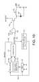
- FIG. 10shows control circuitry according to an embodiment of the present invention wherein the switching circuitry charges the charging element while the reference frequency is above the oscillator frequency.
- FIG. 11shows example waveforms illustrating an embodiment of the present invention including the frequency of the oscillator signal, the frequency of the reference signal, and the regulated voltage supplied to the system circuitry.
- FIG. 12is a flow diagram according to an embodiment of the present invention wherein prior to the power mode changing, a hysteresis threshold of the voltage regulator is adjusted to pre-compensate for the change in load current associated with the power mode changing.
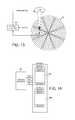
- FIG. 13shows a disk drive including control circuitry employing a switching voltage regulator according to an embodiment of the present invention.
- FIG. 14shows a solid state drive including control circuitry employing a switching voltage regulator according to an embodiment of the present invention.
- FIG. 1Ashows an embodiment of the present invention comprising a switching voltage regulator including a charging element 2 operable to generate an output voltage 4 , switching circuitry 6 coupled to the charging element 2 , and switch control circuitry 8 operable to control the switching circuitry 6 to configure the charging element 2 during a cycle, including to charge the charging element 2 for an on-time, discharge the charging element 2 for a discharge time, and tristate the charging element 2 for a tristate time.
- the on-timeis initialized to a first on-time, and a first switch time is measured comprising the first on-time and a first discharge time of a first cycle.
- a first tristate time of the first cycleis also measured, and a first ratio of the first tristate time to the first switch time is determined.
- the first ratiois compared to a first ratio threshold, and the on-time is decreased to a second on-time if the first ratio exceeds the first ratio threshold. Prior to a power mode changing which increases the current demand of the load, the on-time is increased to the first on-time.
- the charging element 2comprises an inductor, which may be implemented as a discrete or integrated element; however, any suitable charging element may be employed.
- the output voltage 4is applied to system circuitry 11 and to a voltage comparator 10 , which compares the output voltage 4 to a reference voltage 12 .
- the reference voltage 12is selected relative to the target output voltage 4 , and it may be adjusted relative to the system circuitry's 11 mode of operation. For example, the reference voltage 12 may be reduced during modes of operation that require less power (e.g., slower data rate in a communication channel).
- the switch control circuitry 8when the output voltage 4 falls below the reference voltage 12 , the resulting error signal 14 triggers the switch control circuitry 8 to begin a cycle by turning on a FET 6 A to charge the charging element 2 for the on-time, thereby building a charge across a capacitor 16 .
- the switch control circuitry 8turns off the FET 6 A so that the inductor current discharges while recirculating through a diode 6 B to ground.
- the diode 6 Bstops conducting, thereby preventing the output capacitor 16 from discharging through the inductor 2 to ground.
- the inductor 2remains in this tristate condition during the tristate time until the output voltage 4 falls below the reference voltage 12 (and the error signal turns positive), as shown in FIG. 2A .
- the diode 6 Bis replaced with a FET and a current sensor, wherein the FET is turned off when the current sensor detects zero current flowing through the FET at the end of the discharge time.
- the error signal 14may be generated in any suitable manner.
- FIG. 1Bshows an embodiment of the present invention wherein the error signal 14 is generated by a cycle comparator 18 which compares a propagation oscillation signal 20 to a reference oscillation signal 22 output by a frequency generator 24 .
- An oscillator 26generates the propagation oscillation signal 20 which represents a propagation delay of a digital circuit within the system circuitry 11 .
- the error signal 14may represent a phase or frequency error between the propagation oscillation signal 20 and the reference oscillation signal 22 output by the frequency generator 24 .
- FIG. 2Bis a state diagram illustrating how the on-time is adjusted according to an embodiment of the present invention.
- Operation of the discontinuous switching voltage regulatorbegins in STATE 1 where the on-time is initialized to a first on-time.
- the first on-timeis selected to maximize the peak inductor current while preventing damage to the FET 6 A (e.g., an on-time that corresponds to the maximum peak current the FET 6 A can handle minus a predetermined margin).
- a first switch time (T SW )is measured comprising the first on-time (T ON ) and a first discharge time (T REC ) of the inductor 2 .
- a first tristate time of the first cycleis also measured, and a first ratio (T TRI /T SW ) of the first tristate time to the first switch time is determined at branch 28 . If the first ratio is greater than a first ratio threshold (e.g., 3) at branch 28 , then at step 30 the on-time (T ON ) is adjusted to a second on-time by reducing the on-time by 25%, and the state changes to STATE 2. Otherwise, the on-time (T ON ) is not adjusted and the state remains in STATE 1. Any suitable value may be selected for the ratio threshold. For example, the first ratio threshold may be selected relative to the number of states in the state diagram, and/or relative to the range of on-times.
- a first ratio thresholde.g., 3
- a second switch time (T SW )is measured comprising the second on-time (T ON ) and a second discharge time (T REC ) of the inductor 2 .
- a second tristate time (T TRI ) of the second cycleis also measured, and a second ratio (T TRI /T SW ) of the second tristate time to the second switch time is determined at branch 32 . If the second ratio is greater than a second ratio threshold (e.g., 3) at branch 32 , then at step 34 the on-time (T ON ) is adjusted to a third on-time by reducing the on-time by 25%, and the state changes to STATE 3.
- a second ratio thresholde.g., 3
- the second on-timeis approximately 1/N times the first on-time
- the third on-timeis approximately 1/N times the second on-time, and so on for the on-time of the following states. If the second ratio is not greater than the second ratio threshold at branch 32 , then the second ratio is compared to a third ratio threshold (e.g., 0.75) at branch 36 . If the second ratio is less than the third ratio threshold at branch 36 , then the on-time is reset to the first on-time, and the state changes to STATE 1. Otherwise, the on-time (T ON ) is not adjusted, and the state remains in STATE 2. Assuming the state changes to STATE 3, a third switch time and a third tristate time are measured during a third cycle, a similar ratio generated and compared to a third ratio threshold at step 38 , and the on-time adjusted accordingly at step 40 .
- a third ratio thresholde.g. 0.5
- the state diagram of FIG. 2Bmay comprise any suitable number of states, and may also be modified in any suitable manner. Adjusting the on-time relative to the ratio of the tristate time to the switch time may improve the transient response without requiring an analog current sensor or a programmable analog current comparator as in the prior art.
- FIG. 3Ashows circuitry for implementing a discontinuous switching voltage regulator according to an embodiment of the present invention, wherein the error signal 14 is generated by comparing a propagation oscillation signal 20 to a reference oscillation signal 22 .
- the circuitry disclosed in FIG. 3Amay also be employed in an embodiment wherein the error signal 14 is generated using a different method, for example, by comparing the output voltage 4 to a reference voltage 12 as shown in FIG. 1A .
- the circuitry in FIG. 3Acomprises state mapper circuitry 42 for implementing the state diagram of FIG. 2B , and state controller circuitry 44 for generating three state signals S0, S1 and S2 corresponding to three states of the switching voltage regulator T TRI , T ON , and T REC .
- the state mapper circuitry 42may comprise any suitable circuitry for implementing the state diagram of FIG. 2B , such as a suitable state machine together with suitable math operators (multipliers, dividers, etc.) and/or code segments of a control program executed by a microprocessor.
- a power-on-reset (POR) signal 46is held high turning FET 6 A on through OR gate 48 until the output voltage 4 rises sufficiently for the oscillator 26 to function properly.
- POR 46is reset, the FET 6 A is turned off.
- the state controller 44is enabled via control signal 50 output by AND gate 51 .
- the state controller 44has been initialized to state S0 (tristate time of FIG. 2A ).
- the state controller 44transitions from state S0 to state S1 (on-time of FIG. 2A ), which turns on FET 6 A via control signal 52 and enables via control signal 54 a digital timer (counter) 56 to begin timing the switch time (T SW ).
- the state controller 44also loads the on-time 58 generated by the state mapper 42 into a counter 60 (via control line 61 ) and enables the counter 60 via control line 63 .
- the counter 60generates a DONE signal 62 at the end of the on-time.
- the state controller 44transitions from state S1 to state S2, loads a maximum discharge time into counter 60 , and begins monitoring the voltage 64 across the diode 6 B to detect the end of the discharge time.
- the maximum discharge timeis related to the inductor drive voltage (input voltage of the battery minus the output voltage Vdd in FIG. 1 ), and the flyback voltage that discharges the inductor 2 (Vdd plus the voltage across the diode 6 B). If the input voltage is much higher than the output voltage (plus the reverse bias voltage caused by the flyback diode), then the maximum off time is selected to be longer than the on-time.
- the state controller 44transitions from state S2 to state S0 and enables via control signal 66 a digital timer (counter) 68 for timing the next tristate time (T TRI ), and stops the counter 56 .
- the state controller 44loads via control signal 52 the switch time (T SW ) and the tristate time (T TRI ) into the state mapper 42 , which generates the next on-time according to the state diagram of FIG. 2B .
- the state mapper 42generates the next on-time in a manner that compensates for the delay in computing the next on-time.
- FIG. 3Bshows circuitry for implementing the state controller 44 of FIG. 3A according to an embodiment of the present invention.
- the 2-bit counter 70is initialized to state S0 by the enable signal 50 (see FIG. 3A ).
- the 2-bit counter 70is enabled by a multiplexer 76 when the switching voltage regulator transitions into the next state. For example, when in state S0, the multiplexer 76 outputs control signal 78 as the enable signal 80 to the 2-bit counter 70 .
- control signal 78enables the 2-bit counter 70 which transitions from state S0 to state S1.
- the multiplexer 76enables the 2-bit counter 70 which transitions from state S1 to state S2.
- a latch 82is used to detect the low to high transition of voltage 64 at the end of the discharge time.
- the latch 82When the voltage 64 transitions from high to low at the end of the on-time, the latch 82 enables an AND gate 84 which then detects the transition from low to high at the end of the discharge time. Alternatively, an AND gate 86 detects if the counter 60 ( FIG. 3A ) times out before the voltage 64 transitions from low to high. An OR gate 88 outputs the control signal 90 indicating the end of the discharge time, which enables the 2-bit counter 70 to transition from state S2 back to state S0 which activates control signal 66 to begin timing the tristate time.
- FIGS. 4A-4Dillustrate operation of the switching voltage regulator, including the inductor current, load current, error signal, data rate, and output voltage.
- the error signalis high and the state mapper 42 remains in STATE 1 ( FIG. 2B ) until the output voltage rises to an operating level. Once the output voltage stabilizes, the state mapper 42 reduces the on-time and transitions into STATE 2 and then into STATE 3.
- the state mapper 42reduces the on-time and transitions into STATE 4.
- the state mapper 42resets the on-time to the maximum and transitions into STATE 1 as shown in FIG.
- FIG. 5Ais a flow diagram according to an embodiment of the present invention wherein prior to a power mode changing (step 92 ) which increases the current demand of the load (step 94 ), the on-time of the charging element is increased (step 96 ) by decreasing the current state in FIG. 2B . For example, if the current state is STATE 3, the on-time is increased by 4/3 and the state is decreased to STATE 2. In this manner, the charging element (inductor 2 ) will be charged with more current just prior to the power mode changing which helps compensate for the increase in the current demand of the load.
- Pre-adjusting by increasing the on-timereduces the required voltage margin by reducing the supply voltage undershoot as shown in FIG. 5B leading to a more efficient switching voltage regulator.
- the voltage undershootmay be further reduced toward zero or even inverted by further increasing the on-time of the charging element.
- FIG. 5Aalso illustrates an embodiment of the present invention wherein prior to a power mode changing (step 92 ) which decreases the current demand of the load (step 94 ), the on-time of the charging element is decreased (step 100 ) by increasing the current state in FIG. 2B .
- the current stateis STATE 3
- the on-timeis decreased by 3 ⁇ 4 and the state is increased to STATE 4.
- the charging elementinductor 2
- Pre-adjusting by decreasing the on-timereduces the supply voltage overshoot leading to a more efficient switching voltage regulator.
- FIGS. 6A-6Dillustrate operation of the switching voltage regulator similar to FIGS. 4A-4D described above, with the addition of the pre-adjust compensation for a power mode change.
- the on-timeis pre-adjusted one cycle before the power mode changes (current demand decreases) due to the data rate decreasing, and then it is pre-adjusted one cycle before the power mode changes (current demand increases) due to the data rate increasing as shown in FIG. 6C .
- thisreduces the undershoot and overshoot of the error signal as compared to FIG. 4B
- FIG. 6Dit improves the transient response of the supply voltage as compared to FIG. 4D by more closely matching the on time of the switch to the expected load change.
- This approachalso reduces the lag time between a request for higher voltage, and the regulator's compliance with that request (supply voltage latency).
- FIG. 7shows a switching voltage regulator operable to regulate a voltage 104 supplied to system circuitry 106 .
- the switching voltage regulatorcomprises a ring oscillator 108 operable to generate an oscillator signal 110 representing a gate speed of a reference circuit in the system circuitry 106 , wherein the ring oscillator 108 comprises a plurality of delay elements connected in series.
- a frequency generator 112generates a reference signal 114 representing a target gate speed of the reference circuit, wherein a frequency of the reference signal 114 is based on a divider value.
- a comparator 116compares the oscillator signal 110 to the reference signal 114 , and switching circuitry 118 (controlled by a switch controller 120 ) charges a charging element 122 in response to the comparison.
- Control circuitry 124adjusts the number of delay elements in the ring oscillator 108 and the divider value of the frequency generator 112 to generate hysteresis in the comparison. Prior to a power mode of the system circuitry changing, a hysteresis threshold is adjusted for controlling a level of the hysteresis.
- control circuitry 124 of FIG. 7may comprise a flip-flop having an output 126 that changes state each time the output 128 of the comparator 116 changes state.
- the output 128 of the comparator 116goes high each time a frequency of the oscillator signal 110 falls below a frequency of the reference signal 114 .
- the output 126 of the flip-flop 124configures a multiplexer 130 to toggle between two divider values (N and M), and adjusts the number of delay elements in the ring oscillator 108 .
- the control circuitry 124may also comprise suitable delay circuitry to accommodate for the timing characteristics of the switching circuitry 118 .
- FIG. 8shows an embodiment of a ring oscillator 108 according to an embodiment of the present invention comprising a plurality of delay elements 132 0 - 132 N (including a plurality of inverters) which are powered by the supply voltage 104 generated by the switching voltage regulator.
- the ring oscillator 108further comprises a NAND gate 134 having as inputs the output of the last delay element 132 N and an enable signal 136 .
- the enable signal 136When the enable signal 136 is active, the enable signal 136 will propagate through the delay elements 132 0 - 132 N and eventually feedback to the NAND gate 134 , thereby generating the oscillator signal 110 having a frequency that is proportional to the supply voltage 104 .
- the frequency of the oscillator signal 110is adjusted by adjusting the number of delay elements 132 0 - 132 N connected in series.
- the flip-flop signal 126controls a multiplexer 138 to selectively remove/insert delay element 132 1 in order to make a coarse adjustment to the frequency of the oscillator signal 110 .
- the coarse adjustment to the frequency of the reference signal 114(e.g., by changing the divider value between N and M) is slightly different than the coarse adjustment to the frequency of the oscillator signal 110 (e.g., by changing the number of delay elements) so that the result is a fine adjustment to the threshold in comparator 116 ( FIG. 7 ). Toggling between the two adjusted frequencies thereby introduces a hysteresis in the comparator 116 which increases the efficiency by reducing the peak current relative to the normal load current.
- the fractional adjustment to the comparison thresholdmay be computed as: (( d ⁇ 1)/ d )*( n /( n ⁇ 1)) where d is the divider value of the frequency generator 112 , and n is the number of delay elements in the ring oscillator 108 .
- dthe divider value of the frequency generator 112
- nthe number of delay elements in the ring oscillator 108 .
- any suitable charging elemente.g., an inductor, a capacitor, etc.
- a buck mode voltage regulatoris shown employing an inductor 122 as the charging element.
- the switching voltage regulatormay include a boost mode voltage regulator, or a buck/boost mode voltage regulator.
- the physical location of the elements comprising the switching voltage regulatoris unimportant.
- the ring oscillator 108may be located on a separate chip from the system circuitry 106 .
- the inductor 122may be located separately from digital circuitry comprising portions of the switching voltage regulator.
- system circuitry 106may comprise any circuitry supplied by a voltage.
- the system circuitry 106may comprise a microprocessor, as would be typically found in a computer.
- the system circuitry 106may comprise analog circuitry configured to perform one or more tasks.
- the ring oscillator 108is configurable to represent one of a plurality of different circuits (or circuit paths) within the system circuitry 106 depending on a mode of operation (i.e., the reference circuit may be different circuits at different times).
- the oscillator frequencyneed not correspond precisely with the gate speed of the reference circuit, but may instead simply track it (e.g., the oscillator frequency may be a multiple of the corresponding gate speed-equivalent frequency of the reference circuit).
- the oscillator frequencyis directly proportional to the gate speed of the reference circuit. Since the oscillator frequency will vary relative to the magnitude of the supply voltage 104 as well as other factors, such as temperature, adjusting the magnitude of the supply voltage 104 adjusts the frequency of the oscillator signal 110 until the reference circuit is operating at the desired gate speed.
- the simulation and layout software used in the design of the system circuitry 106may provide sophisticated timing analysis of various delays.
- the reference circuit within the system circuitry 106is determined at design time using the simulation and layout software.
- the gates in the ring oscillator 108 and system circuitry 106may be fabricated together so they have similar characteristics. Some differences may occur due to loading effects and wire routing; however, by adding inverters, lengthening wires through physical placement, adding dummy loads, and placing the ring oscillator 108 as close as possible to the reference circuit, the ring oscillator 108 may be configured to substantially match the delay of the reference circuit.
- the ring oscillator 108will change speed as the temperature changes, as the supply voltage 104 changes, or as the manufacturing process produces faster or slower gates, and thereby track the propagation delay of the reference circuit within the system circuitry 106 .
- FIG. 9shows an example embodiment of the present invention including circuitry for implementing the comparator 116 for comparing at least one cycle of the oscillator signal 110 to at least one cycle of the reference signal 114 .
- the comparator 116comprises a first register 140 (e.g., a first counter) clocked by the reference signal 114 , wherein the first register 140 asserts a first signal 142 at the end of the reference cycle, and a second register 144 (e.g., a second counter) clocked by the oscillator signal 110 , wherein the second register 144 asserts a second signal 146 at the end of the oscillator cycle.
- the comparator 116further comprises a latch 148 for latching the first signal 142 if generated before the second signal 146 . Latch 148 thus outputs a reference fast (REF_FAST) signal 150 indicating when the reference signal 114 is oscillating faster than the oscillator signal 110 .
- REF_FASTreference fast
- an OR gate 152asserts a disable signal 154 through latches 156 and 158 .
- the disable signal 154latches the output of latch 148 through AND gate 160 , and disables the latch 148 through AND gate 162 until the next sample period.
- the disable signal 154also disables the ring oscillator 108 and loads the counters 140 and 144 with appropriate starting values.
- a register 164resets the disable signal 154 when clocked by the reference signal 114 to thereby synchronize the ring oscillator 108 and the frequency generator 112 .
- the comparator 116compares one cycle of the oscillator signal 110 to one cycle of the reference signal 114 . Because the comparator 116 compares a cycle (or cycles) of the oscillator signal 110 to a cycle (or cycles) of the reference signal 114 , as compared to computing a frequency difference using counters, the comparator 116 may in some embodiments reduce the transport delay and quantization error, and thereby improve the transient response of the switching voltage regulator.
- the counters 140 and 144 in the embodiment of FIG. 9enable scaling of the oscillator frequency or the reference frequency. For example, if the frequency of the oscillator signal 110 should equal half the frequency of the reference signal 114 , then counter 140 is loaded with a starting value that is twice the starting value loaded into counter 144 , from which values the two counters count down at each cycle of the reference and oscillator signals.
- the comparator 116compares multiple cycles of the oscillator signal 110 and reference signal 114 in order to improve the accuracy of the measurement, for example, by compensating for startup transient errors of the ring oscillator 108 .
- counters 140 and 144are loaded with a starting value of 2 in order to compare two cycles of the oscillator signal 110 to two cycles of the reference signal 114 .
- the counters 140 and 144are implemented using simple registers for detecting a single cycle of the reference signal 114 and oscillator signal 110 , respectively.
- FIG. 10shows a switching voltage regulator employing a ring oscillator 108 and comparator 116 according to an embodiment of the present invention.
- the REF_FAST signal 150When the REF_FAST signal 150 is active (indicating that the output voltage 104 is too low), it turns on switch 118 through OR gate 166 so as to charge the charging element 122 .
- the REF_FAST signal 150also toggles flip-flop 124 so as to adjust the divider value of the frequency generator 112 and the number of delay elements in the ring oscillator 108 to effectively raise the threshold in the comparator 116 .
- the switch 118remains on until the oscillator signal 110 rises above the higher threshold, at which time the REF_FAST signal 150 goes low turning off the switch 118 to stop charging the charging element 122 .
- the REF_FAST signal 150goes low, it also toggles flip-flop 124 so as to lower the threshold in the comparator 116 , thereby keeping switch 118 off until the oscillator signal 110 falls back below the
- the switching voltage regulator of FIG. 10comprises a diode 168 that enables a recirculation current.
- the diode 168 of FIG. 10is replaced with a conventional switch (e.g., a FET, as shown in FIG. 7 ) to improve efficiency by avoiding the voltage drop of the diode 168 .
- a current detectoris employed to turn off the switch once the current decays to zero.
- the switching voltage regulatorfurther comprises suitable circuitry to facilitate a startup operation during a power-on restart (POR) event.
- PORpower-on restart
- a POR signal 170enables a charge cycle through OR gate 166 regardless of the discharge level of the current in order to help maintain a sufficient output voltage 104 during the startup operation. Once the switching voltage regulator stabilizes, the POR signal 170 is disabled so that the regulator enters the discontinuous mode.
- FIG. 11shows example waveforms illustrating an embodiment of the present invention including the frequency of the oscillator signal 110 , the frequency of the reference signal 114 , and the regulated voltage 104 supplied to the system circuitry 106 .
- the control circuitry 124decreases the number of delay elements in the ring oscillator 108 which effectively increases the frequency of the oscillator signal 110 as shown in FIG. 11 .
- the control circuitry 124adjusts the divider value of the frequency generator 112 which increases the frequency of the reference signal 114 to be slightly higher than the frequency of the oscillator signal 110 as illustrated in FIG. 11 . This causes the comparator 116 to turn on switch 118 of FIG.
- the control circuitry 124increases the number of delay elements in the ring oscillator 108 which effectively decreases the frequency of the oscillator signal 110 as illustrated in FIG. 11 .
- the control circuitry 124adjusts the divider value of the frequency generator 112 which decreases the frequency of the reference signal 114 to be slightly lower than the frequency of the oscillator signal 110 as illustrated in FIG. 11 . This causes the comparator 116 to turn off switch 118 of FIG. 10 which eventually discharges the charging element 122 until the supply voltage 104 decreases to start another cycle.
- the on time of switch 118decreases which reduces the ripple voltage of the supply voltage 104 .
- FIG. 12shows a flow diagram according to an embodiment of the present invention wherein prior to a power mode changing (step 172 ) which increases the current demand of the load (step 174 ), the hysteresis threshold is increased (step 176 ) to increase the on-time of the charging element. Similar to decreasing the state in FIG. 2B as described above, increasing the hysteresis threshold reduces the required voltage margin by reducing the supply voltage undershoot when the power mode changes. In another embodiment, prior to the power mode changing (step 172 ) which decreases the current demand of the load (step 174 ), the hysteresis threshold is decreased (step 178 ) to decrease the on-time of the charging element. Similar to increasing the state in FIG. 2B as described above, decreasing the hysteresis threshold reduces supply voltage overshoot when the power mode changes leading to a more efficient switching voltage regulator.
- the hysteresis thresholdmay be adjusted using any suitable technique.
- the hysteresis thresholdis adjusted by adjusting the divider value of the frequency generator 112 , and/or by adjusting the number of delay elements in the ring oscillator 108 .
- the hysteresis thresholdis adjusted by adjusting the value loaded into the counter 140 clocked by the reference signal 114 and/or by adjusting the value loaded into the counter 144 clocked by the oscillator signal 110 .
- the hysteresis thresholdmay be increased by decreasing the value loaded into the counter 140 clocked by the reference signal 114 , and/or by increasing the value loaded into the counter 144 clocked by the oscillator signal 110 .
- the switching voltage regulator of the present inventionmay be employed in any suitable device, such as in a data storage device.
- FIG. 13shows a disk drive comprising a head 180 actuated over a disk 182 and control circuitry 184 including a switching voltage regulator described above according to an embodiment of the present invention.
- FIG. 14shows a solid state drive comprising a plurality of non-volatile semiconductor memories 186 A, 186 B, etc., such as flash memories, and control circuitry 188 including a switching voltage regulator described above according to an embodiment of the present invention.
- the switching voltage regulator of the present inventionmay also be employed in any suitable consumer or industrial electronic device other than storage devices.
- the switching voltage regulatormay be employed in system circuitry for computers, cell phones, televisions, music players, or any other suitable device.
Landscapes
- Engineering & Computer Science (AREA)
- Power Engineering (AREA)
- Dc-Dc Converters (AREA)
Abstract
Description
((d−1)/d)*(n/(n−1))
where d is the divider value of the
16/17* 16/15=1.004
In one embodiment, employing a coarser granularity for (d,n) reduces noise in the
Claims (20)
Priority Applications (1)
| Application Number | Priority Date | Filing Date | Title |
|---|---|---|---|
| US12/534,072US8912778B1 (en) | 2006-03-30 | 2009-07-31 | Switching voltage regulator employing current pre-adjust based on power mode |
Applications Claiming Priority (2)
| Application Number | Priority Date | Filing Date | Title |
|---|---|---|---|
| US11/393,425US7486060B1 (en) | 2006-03-30 | 2006-03-30 | Switching voltage regulator comprising a cycle comparator for dynamic voltage scaling |
| US12/534,072US8912778B1 (en) | 2006-03-30 | 2009-07-31 | Switching voltage regulator employing current pre-adjust based on power mode |
Publications (1)
| Publication Number | Publication Date |
|---|---|
| US8912778B1true US8912778B1 (en) | 2014-12-16 |
Family
ID=40298074
Family Applications (2)
| Application Number | Title | Priority Date | Filing Date |
|---|---|---|---|
| US11/393,425Active2027-02-01US7486060B1 (en) | 2006-03-30 | 2006-03-30 | Switching voltage regulator comprising a cycle comparator for dynamic voltage scaling |
| US12/534,072Active2033-03-12US8912778B1 (en) | 2006-03-30 | 2009-07-31 | Switching voltage regulator employing current pre-adjust based on power mode |
Family Applications Before (1)
| Application Number | Title | Priority Date | Filing Date |
|---|---|---|---|
| US11/393,425Active2027-02-01US7486060B1 (en) | 2006-03-30 | 2006-03-30 | Switching voltage regulator comprising a cycle comparator for dynamic voltage scaling |
Country Status (1)
| Country | Link |
|---|---|
| US (2) | US7486060B1 (en) |
Cited By (7)
| Publication number | Priority date | Publication date | Assignee | Title |
|---|---|---|---|---|
| US20130169239A1 (en)* | 2011-12-28 | 2013-07-04 | Honda Motor Co., Ltd. | Electric power generation control system for vehicle |
| US20140253056A1 (en)* | 2013-03-11 | 2014-09-11 | Cree, Inc. | Power Supply with Adaptive-Controlled Output Voltage |
| US20150160975A1 (en)* | 2013-12-09 | 2015-06-11 | Advanced Micro Devices, Inc. | Voltage droop mitigation in 3d chip system |
| US9425687B2 (en) | 2013-03-11 | 2016-08-23 | Cree, Inc. | Methods of operating switched mode power supply circuits using adaptive filtering and related controller circuits |
| US10211738B2 (en)* | 2017-05-17 | 2019-02-19 | Semiconductor Manufacturing International (Shanghai) Corp. | DC-DC conversion circuit system and forming method thereof |
| US10236773B2 (en) | 2016-09-30 | 2019-03-19 | Cypress Semiconductor Corporation | Low quiescent current DC-to-DC converter with increased output voltage accuracy |
| US20190140542A1 (en)* | 2017-10-30 | 2019-05-09 | Renesas Electronics America Inc. | Asynchronous controller for low power hysteretic buck-boost dc-dc controller |
Families Citing this family (143)
| Publication number | Priority date | Publication date | Assignee | Title |
|---|---|---|---|---|
| US8079045B2 (en) | 2001-10-17 | 2011-12-13 | Keen Personal Media, Inc. | Personal video recorder and method for inserting a stored advertisement into a displayed broadcast stream |
| US7486060B1 (en)* | 2006-03-30 | 2009-02-03 | Western Digital Technologies, Inc. | Switching voltage regulator comprising a cycle comparator for dynamic voltage scaling |
| US7551383B1 (en) | 2006-06-28 | 2009-06-23 | Western Digital Technologies, Inc. | Adjusting voltage delivered to disk drive circuitry based on a selected zone |
| US20080278223A1 (en)* | 2006-11-22 | 2008-11-13 | Kent Kernahan | Apparatus and method for controlling the propagation delay of a circuit by controlling the voltage applied to the circuit |
| US20080116964A1 (en)* | 2006-11-22 | 2008-05-22 | Kent Kernahan | Apparatus and method for controlling the propagation delay of a circuit by controlling the voltage applied to the circuit |
| US7847529B2 (en)* | 2007-08-30 | 2010-12-07 | International Business Machines Corporation | Dual loop linear voltage regulator with high frequency noise reduction |
| US7855534B2 (en)* | 2007-08-30 | 2010-12-21 | International Business Machines Corporation | Method for regulating a voltage using a dual loop linear voltage regulator with high frequency noise reduction |
| US7733189B1 (en) | 2007-09-14 | 2010-06-08 | Western Digital Technologies, Inc. | Oscillator comprising foldover detection |
| US20090113702A1 (en) | 2007-11-01 | 2009-05-07 | Western Digital Technologies, Inc. | Disk drive comprising a double sided flex circuit wherein a first side lead provides an etching mask for a second side lead |
| US8085020B1 (en)* | 2008-06-13 | 2011-12-27 | Western Digital Technologies, Inc. | Switching voltage regulator employing dynamic voltage scaling with hysteretic comparator |
| US9009358B1 (en) | 2008-09-23 | 2015-04-14 | Western Digital Technologies, Inc. | Configuring a data storage device with a parameter file interlocked with configuration code |
| US8914625B1 (en) | 2009-07-31 | 2014-12-16 | Western Digital Technologies, Inc. | Automatically configuring a web browser file when booting an operating system from a data storage device |
| US9330715B1 (en) | 2010-03-22 | 2016-05-03 | Western Digital Technologies, Inc. | Mapping of shingled magnetic recording media |
| US8687306B1 (en) | 2010-03-22 | 2014-04-01 | Western Digital Technologies, Inc. | Systems and methods for improving sequential data rate performance using sorted data zones |
| US9268499B1 (en) | 2010-08-13 | 2016-02-23 | Western Digital Technologies, Inc. | Hybrid drive migrating high workload data from disk to non-volatile semiconductor memory |
| US8879188B1 (en) | 2010-08-23 | 2014-11-04 | Western Digital Technologies, Inc. | Disk drive employing fly height calibration tracks to account for magnetic entropy and thermal decay |
| US8937404B1 (en) | 2010-08-23 | 2015-01-20 | Western Digital Technologies, Inc. | Data storage device comprising dual mode independent/parallel voltage regulators |
| US8954664B1 (en) | 2010-10-01 | 2015-02-10 | Western Digital Technologies, Inc. | Writing metadata files on a disk |
| US8324974B1 (en) | 2010-12-17 | 2012-12-04 | Western Digital Technologies, Inc. | Regulating power consumption of digital circuitry using a multi-layer ring oscillator |
| US8390367B1 (en) | 2011-02-15 | 2013-03-05 | Western Digital Technologies, Inc. | Ensuring minimum gate speed during startup of gate speed regulator |
| US8350628B1 (en) | 2011-02-15 | 2013-01-08 | Western Digital Technologies, Inc. | Gate speed regulator dithering ring oscillator to match critical path circuit |
| US9268649B1 (en) | 2011-06-23 | 2016-02-23 | Western Digital Technologies, Inc. | Disk drive with recent write streams list for data refresh determination |
| US8990493B1 (en) | 2011-06-30 | 2015-03-24 | Western Digital Technologies, Inc. | Method and apparatus for performing force unit access writes on a disk |
| US9189392B1 (en) | 2011-06-30 | 2015-11-17 | Western Digital Technologies, Inc. | Opportunistic defragmentation during garbage collection |
| US8909889B1 (en) | 2011-10-10 | 2014-12-09 | Western Digital Technologies, Inc. | Method and apparatus for servicing host commands by a disk drive |
| US9158722B1 (en) | 2011-11-02 | 2015-10-13 | Western Digital Technologies, Inc. | Data storage device to communicate with a host in a SATA or a USB mode |
| US9213493B1 (en) | 2011-12-16 | 2015-12-15 | Western Digital Technologies, Inc. | Sorted serpentine mapping for storage drives |
| US9063838B1 (en) | 2012-01-23 | 2015-06-23 | Western Digital Technologies, Inc. | Data storage device shifting data chunks of alignment zone relative to sector boundaries |
| US8996839B1 (en) | 2012-01-23 | 2015-03-31 | Western Digital Technologies, Inc. | Data storage device aligning partition to boundary of sector when partition offset correlates with offset of write commands |
| US9155139B2 (en) | 2012-03-09 | 2015-10-06 | Rockwell Automation Technologies, Inc. | LED driver circuits and methods |
| US8749910B1 (en) | 2012-05-07 | 2014-06-10 | Western Digital Technologies, Inc. | Hard disk drive assembly including a NVSM to store configuration data for controlling disk drive operations |
| US8681442B2 (en) | 2012-05-11 | 2014-03-25 | Western Digital Technologies, Inc. | Disk drive comprising extended range head proximity sensor |
| US9128820B1 (en) | 2012-06-18 | 2015-09-08 | Western Digital Technologies, Inc. | File management among different zones of storage media |
| US9383923B1 (en) | 2012-10-18 | 2016-07-05 | Western Digital Technologies, Inc. | Write pointer management for a disk drive |
| US8970978B1 (en) | 2012-10-22 | 2015-03-03 | Western Digital Technologies, Inc. | Disk drive detecting head touchdown by applying DC+AC control signal to fly height actuator |
| US8959281B1 (en) | 2012-11-09 | 2015-02-17 | Western Digital Technologies, Inc. | Data management for a storage device |
| US8902529B1 (en) | 2012-11-20 | 2014-12-02 | Western Digital Technologies, Inc. | Dual frequency crystal oscillator |
| US9086708B2 (en) | 2012-12-31 | 2015-07-21 | Gazelle Semiconductor Inc. | High slew rate switching regulator circuits and methods |
| US9735574B2 (en) | 2012-12-31 | 2017-08-15 | Gazelle Semiconductor, Inc. | Switching regulator circuits and methods |
| US8941941B1 (en) | 2013-02-28 | 2015-01-27 | Western Digital Technologies, Inc. | Disk drive calibrating touchdown sensor |
| US8891341B1 (en) | 2013-03-11 | 2014-11-18 | Western Digital Technologies, Inc. | Energy assisted magnetic recording disk drive using modulated laser light |
| US9417628B2 (en) | 2013-03-13 | 2016-08-16 | Western Digital Technologies, Inc. | Production failure analysis system |
| US9074941B1 (en) | 2013-03-14 | 2015-07-07 | Western Digital Technologies, Inc. | Systems and methods for measuring ambient and laser temperature in heat assisted magnetic recording |
| US9053749B1 (en) | 2013-03-15 | 2015-06-09 | Western Digital Technologies, Inc. | Disk drive comprising a per-drive and per-head fly height filter |
| US8922939B1 (en) | 2013-04-02 | 2014-12-30 | Western Digital Technologies, Inc. | Disk drive generating feed-forward fly height control based on temperature sensitive fly height sensor |
| US9064542B1 (en) | 2013-04-08 | 2015-06-23 | Western Digital Technologies, Inc. | Scheduled load of heads to reduce lubricant migration on pole tip and decrease time to ready |
| US8949521B1 (en) | 2013-04-10 | 2015-02-03 | Western Digital Technologies, Inc. | Actuator prepositioning for disk drive |
| US8947816B1 (en) | 2013-05-01 | 2015-02-03 | Western Digital Technologies, Inc. | Data storage assembly for archive cold storage |
| US8891193B1 (en) | 2013-05-09 | 2014-11-18 | Western Digital Technologies, Inc. | Disk drive calibrating threshold and gain of touchdown sensor |
| US9153287B1 (en) | 2013-05-13 | 2015-10-06 | Western Digital Technologies, Inc. | Data access for shingled magnetic recording media |
| US9183864B1 (en) | 2013-06-13 | 2015-11-10 | Western Digital Technologies, Inc. | Disk drive adjusting closed-loop fly height target based on change in open-loop fly height control signal |
| US9164694B1 (en) | 2013-06-19 | 2015-10-20 | Western Digital Technologies, Inc. | Data storage device detecting read-before-write conditions and returning configurable return data |
| US9577532B2 (en) | 2013-07-25 | 2017-02-21 | Gazelle Semiconductor, Inc. | Switching regulator circuits and methods |
| US9025270B1 (en) | 2013-09-17 | 2015-05-05 | Western Digital Technologies, Inc. | Electronic system with current conservation mechanism and method of operation thereof |
| US9355666B1 (en) | 2013-09-30 | 2016-05-31 | Western Digital Technologies, Inc. | Disk drive measuring stroke difference between heads by detecting a difference between ramp contact |
| US9099144B1 (en) | 2013-10-11 | 2015-08-04 | Western Digital Technologies, Inc. | Disk drive evaluating laser performance for heat assisted magnetic recording |
| US9471072B1 (en) | 2013-11-14 | 2016-10-18 | Western Digital Technologies, Inc | Self-adaptive voltage scaling |
| US9047917B1 (en) | 2013-11-26 | 2015-06-02 | Western Digital Technologies, Inc. | Disk drive slider with sense amplifier for coupling to a preamp through a supply/bias line and a read signal line |
| US9866104B2 (en) | 2013-11-26 | 2018-01-09 | Gazelle Semiconductor, Inc. | Circuits and methods for operating a switching regulator |
| US9064525B2 (en) | 2013-11-26 | 2015-06-23 | Western Digital Technologies, Inc. | Disk drive comprising laser transmission line optimized for heat assisted magnetic recording |
| US9257145B1 (en) | 2013-11-27 | 2016-02-09 | Western Digital Technologies, Inc. | Disk drive measuring down-track spacing of read sensors |
| US9013818B1 (en) | 2013-12-06 | 2015-04-21 | Western Digital Technologies, Inc. | Disk drive measuring reader/writer gap by measuring fractional clock cycle over disk radius |
| US9021410B1 (en) | 2013-12-10 | 2015-04-28 | Western Technologies, Inc. | Electronic system with multi-cycle simulation coverage mechanism and method of operation thereof |
| US8958167B1 (en) | 2013-12-23 | 2015-02-17 | Western Digital Technologies, Inc. | Detection of disk surface irregularities in data storage devices |
| US9501393B2 (en) | 2014-01-27 | 2016-11-22 | Western Digital Technologies, Inc. | Data storage system garbage collection based on at least one attribute |
| US8908311B1 (en) | 2014-01-27 | 2014-12-09 | Western Digital Technologies, Inc. | Data storage device writing a multi-sector codeword in segments over multiple disk revolutions |
| US9864529B1 (en) | 2014-01-27 | 2018-01-09 | Western Digital Technologies, Inc. | Host compatibility for host managed storage media |
| US9064504B1 (en) | 2014-01-29 | 2015-06-23 | Western Digital Technologies, Inc. | Electronic system with media recovery mechanism and method of operation thereof |
| US9230585B1 (en) | 2014-01-31 | 2016-01-05 | Western Digital Technologies, Inc. | Per wedge preheat DFH to improve data storage device performance |
| US9257146B1 (en) | 2014-02-11 | 2016-02-09 | Western Digital Technologies, Inc. | Data storage device comprising sequence detector compensating for inter-track interference |
| US9117489B1 (en) | 2014-02-18 | 2015-08-25 | Western Digital Technologies, Inc. | Data storage device screening heads by verifying defects after defect scan |
| US8988809B1 (en) | 2014-02-18 | 2015-03-24 | Western Digital (Fremont), Llc | Disk recording device for writing a radially coherent reference band by measuring relative timing offsets of reference bursts |
| US9070406B1 (en) | 2014-03-10 | 2015-06-30 | Western Digital Technologies, Inc. | Disk drive configuring one-dimensional and two-dimensional recording areas based on read element spacing |
| US9245556B2 (en) | 2014-03-10 | 2016-01-26 | Western Digital Technologies, Inc. | Disk drive employing multiple read elements to increase radial band for two-dimensional magnetic recording |
| US9082458B1 (en) | 2014-03-10 | 2015-07-14 | Western Digital Technologies, Inc. | Data storage device balancing and maximizing quality metric when configuring arial density of each disk surface |
| US9263088B2 (en) | 2014-03-21 | 2016-02-16 | Western Digital Technologies, Inc. | Data management for a data storage device using a last resort zone |
| US8947812B1 (en) | 2014-03-27 | 2015-02-03 | Western Digital Technologies, Inc. | Data storage device comprising equalizer filter and inter-track interference filter |
| US9916616B2 (en) | 2014-03-31 | 2018-03-13 | Western Digital Technologies, Inc. | Inventory management system using incremental capacity formats |
| US9632711B1 (en) | 2014-04-07 | 2017-04-25 | Western Digital Technologies, Inc. | Processing flush requests by utilizing storage system write notifications |
| US9645752B1 (en) | 2014-04-07 | 2017-05-09 | Western Digital Technologies, Inc. | Identification of data committed to non-volatile memory by use of notification commands |
| US8976633B1 (en) | 2014-04-15 | 2015-03-10 | Western Digital Technologies, Inc. | Data storage device calibrating fly height actuator based on laser power for heat assisted magnetic recording |
| US9123370B1 (en) | 2014-04-15 | 2015-09-01 | Western Digital Technologies, Inc. | Data storage device calibrating fly height actuator based on laser power for heat assisted magnetic recording |
| US8988810B1 (en) | 2014-04-16 | 2015-03-24 | Western Digital Technologies, Inc. | Track measurement for data storage device |
| US9401165B1 (en) | 2014-05-05 | 2016-07-26 | Western Digital Technologies, Inc. | Method and system to monitor magnetic head loading and unloading stability for a data storage system |
| US9245558B1 (en) | 2014-05-09 | 2016-01-26 | Western Digital Technologies, Inc. | Electronic system with data management mechanism and method of operation thereof |
| US9075714B1 (en) | 2014-05-13 | 2015-07-07 | Western Digital Technologies, Inc. | Electronic system with data management mechanism and method of operation thereof |
| US9251856B1 (en) | 2014-05-30 | 2016-02-02 | Western Digial Technologies, Inc. | Read failover method and apparatus for a data storage system |
| US9251844B1 (en) | 2014-06-02 | 2016-02-02 | Western Digital Technologies, Inc. | Waterfall method and apparatus for a data storage device read system |
| US9025267B1 (en) | 2014-06-09 | 2015-05-05 | Western Digital Technologies, Inc. | Data storage device using branch metric from adjacent track to compensate for inter-track interference |
| US9013821B1 (en) | 2014-06-10 | 2015-04-21 | Western Digital Technologies, Inc. | Data storage device employing one-dimensional and two-dimensional channels |
| US8953277B1 (en) | 2014-06-16 | 2015-02-10 | Western Digital Technologies, Inc. | Data storage device writing tracks on a disk with equal spacing |
| US9117463B1 (en) | 2014-06-23 | 2015-08-25 | Western Digital Technologies, Inc. | Data storage device erasing multiple adjacent data tracks to recover from inter-track interference |
| US9171575B1 (en) | 2014-06-23 | 2015-10-27 | Western Digital Technologies, Inc. | Data storage device detecting media defects by writing opposite polarity test pattern |
| US9444340B2 (en) | 2014-06-26 | 2016-09-13 | Gazelle Semiconductor, Inc. | Circuits and methods for providing current to a load |
| US9424864B2 (en) | 2014-07-02 | 2016-08-23 | Western Digital Technologies, Inc. | Data management for a data storage device with zone relocation |
| US9001453B1 (en) | 2014-07-18 | 2015-04-07 | Western Digital Technologies, Inc. | Data storage device calibrating fly height actuator based on read mode touchdown resistance of touchdown sensor |
| US8953269B1 (en) | 2014-07-18 | 2015-02-10 | Western Digital Technologies, Inc. | Management of data objects in a data object zone |
| US9875055B1 (en) | 2014-08-04 | 2018-01-23 | Western Digital Technologies, Inc. | Check-pointing of metadata |
| US10572358B1 (en) | 2014-09-08 | 2020-02-25 | Western Digital Technologies, Inc. | Data management in RAID environment |
| US9153266B1 (en) | 2014-09-11 | 2015-10-06 | Western Digital Technologies, Inc. | Data storage device measuring laser protrusion fly height profile |
| US9600205B1 (en) | 2014-09-22 | 2017-03-21 | Western Digital Technologies, Inc. | Power aware power safe write buffer |
| US9117479B1 (en) | 2014-09-24 | 2015-08-25 | Western Digital Technologies, Inc. | Data storage device calibrating laser write power for heat assisted magnetic recording |
| US9747928B1 (en) | 2014-09-25 | 2017-08-29 | Western Digital Technologies, Inc. | Data storage device modifying write operation when a laser mode hop is detected |
| US9025421B1 (en) | 2014-10-08 | 2015-05-05 | Western Digital Technologies, Inc. | Data storage device adjusting laser input power to compensate for temperature variations |
| US9236086B1 (en) | 2014-10-15 | 2016-01-12 | Western Digital Technologies, Inc. | Methods for reducing operational latency of data storage systems |
| US9099103B1 (en) | 2014-10-21 | 2015-08-04 | Western Digital Technologies, Inc. | Heat assisted magnetic recording withinterlaced high-power heated and low-power heated tracks |
| US9129628B1 (en) | 2014-10-23 | 2015-09-08 | Western Digital Technologies, Inc. | Data management for data storage device with different track density regions |
| US9123382B1 (en) | 2014-10-28 | 2015-09-01 | Western Digital Technologies, Inc. | Non-volatile caching for sequence of data |
| US9230605B1 (en) | 2014-12-01 | 2016-01-05 | Western Digital Technologies, Inc. | Data storage device maximizing areal density based on a target quality metric |
| US10282371B1 (en) | 2014-12-02 | 2019-05-07 | Western Digital Technologies, Inc. | Object storage device with probabilistic data structure |
| US9269393B1 (en) | 2014-12-08 | 2016-02-23 | Western Digital Technologies, Inc. | Electronic system with data refresh mechanism and method of operation thereof |
| US10282096B1 (en) | 2014-12-17 | 2019-05-07 | Western Digital Technologies, Inc. | Identification of data with predetermined data pattern |
| US9281009B1 (en) | 2014-12-18 | 2016-03-08 | Western Digital Technologies, Inc. | Data storage device employing variable size interleave written track segments |
| US9257143B1 (en) | 2014-12-23 | 2016-02-09 | Western Digital Technologies, Inc. | Precautionary measures for data storage device environmental conditions |
| US9842622B1 (en) | 2014-12-23 | 2017-12-12 | Western Digital Technologies, Inc. | Data storage device having improved read failure tolerance |
| US9311939B1 (en) | 2014-12-23 | 2016-04-12 | Western Digital Technologies, Inc. | Write-through media caching |
| US9076474B1 (en) | 2014-12-23 | 2015-07-07 | Western Digital Technologies, Inc. | Data storage device attenuating thermal decay effect on fly height measurement |
| US9257134B1 (en) | 2014-12-24 | 2016-02-09 | Western Digital Technologies, Inc. | Allowing fast data zone switches on data storage devices |
| US10365836B1 (en) | 2015-01-27 | 2019-07-30 | Western Digital Technologies, Inc. | Electronic system with declustered data protection by parity based on reliability and method of operation thereof |
| US9099134B1 (en) | 2015-01-27 | 2015-08-04 | Western Digital Technologies, Inc. | Data storage device employing multiple jog profiles for a butterfly written disk surface |
| US9672107B1 (en) | 2015-02-11 | 2017-06-06 | Western Digital Technologies, Inc. | Data protection for a data storage device |
| US9933955B1 (en) | 2015-03-05 | 2018-04-03 | Western Digital Technologies, Inc. | Power safe write buffer for data storage device |
| US9318137B1 (en) | 2015-03-13 | 2016-04-19 | Western Digital Technologies, Inc. | Data storage device executing retry operation by buffering signal samples at different radial offsets |
| US9196302B1 (en) | 2015-03-18 | 2015-11-24 | Western Digital Technologies, Inc. | Electronic system with media maintenance mechanism and method of operation thereof |
| US9183877B1 (en) | 2015-03-20 | 2015-11-10 | Western Digital Technologies, Inc. | Data storage device comprising two-dimensional data dependent noise whitening filters for two-dimensional recording |
| US9870281B1 (en) | 2015-03-20 | 2018-01-16 | Western Digital Technologies, Inc. | Power loss mitigation for data storage device |
| US9384774B1 (en) | 2015-03-23 | 2016-07-05 | Western Digital Technologies, Inc. | Data storage device calibrating a laser power for heat assisted magnetic recording based on slope of quality metric |
| US9368131B1 (en) | 2015-04-03 | 2016-06-14 | Western Digital (Fremont), Llc | Data storage device employing mirrored cross-track profiles for top and bottom disk surfaces |
| US9502068B1 (en) | 2015-04-08 | 2016-11-22 | Western Digital Technologies, Inc. | Data storage device updating laser power during non-write mode for heat assisted magnetic recording |
| US9361938B1 (en) | 2015-04-16 | 2016-06-07 | Western Digital Technologies, Inc. | Disk defect management for a data storage device |
| US9472219B1 (en) | 2015-05-01 | 2016-10-18 | Western Digital Technologies, Inc. | Data storage device calibrating parameter for heat assisted magnetic recording |
| US9588898B1 (en) | 2015-06-02 | 2017-03-07 | Western Digital Technologies, Inc. | Fullness control for media-based cache operating in a steady state |
| US9466321B1 (en) | 2015-06-05 | 2016-10-11 | Western Digital Technologies, Inc. | Angular position tracking of data accesses to mitigate risk of data loss |
| US9842617B1 (en) | 2015-06-29 | 2017-12-12 | Western Digital Technologies, Inc. | Electronic system with head management mechanism and method of operation thereof |
| US9639287B1 (en) | 2015-06-29 | 2017-05-02 | Western Digital Technologies, Inc. | Write command reporting |
| US9368132B1 (en) | 2015-09-04 | 2016-06-14 | Western Digital Technologies, Inc. | Data storage device employing differential write data signal and differential write pattern signal |
| US9437242B1 (en) | 2015-09-14 | 2016-09-06 | Western Digital Technologies, Inc. | Data storage device employing different frequency preambles in adjacent data tracks |
| US9959052B1 (en) | 2015-09-17 | 2018-05-01 | Western Digital Technologies, Inc. | Media based cache for data storage device |
| US10063257B1 (en) | 2015-11-03 | 2018-08-28 | Western Digital Technologies, Inc. | Data storage device encoding and interleaving codewords to improve trellis sequence detection |
| US10056920B1 (en) | 2015-11-03 | 2018-08-21 | Western Digital Technologies, Inc. | Data storage device encoding and interleaving codewords to improve trellis sequence detection |
| US9761273B1 (en) | 2015-11-03 | 2017-09-12 | Western Digital Technologies, Inc. | Data storage device encoding and interleaving codewords to improve trellis sequence detection |
| KR20200010830A (en) | 2018-07-23 | 2020-01-31 | 삼성전자주식회사 | Switching regulator for dynamically changing output voltage and power supply circuit including the same |
| US11056976B2 (en) | 2019-03-04 | 2021-07-06 | Analog Devices International Unlimited Company | Counter-based frequency hopping switching regulator |
Citations (97)
| Publication number | Priority date | Publication date | Assignee | Title |
|---|---|---|---|---|
| US4164648A (en) | 1978-06-23 | 1979-08-14 | Hewlett-Packard Company | Double vernier time interval measurement using triggered phase-locked oscillators |
| US4298898A (en) | 1979-04-19 | 1981-11-03 | Compagnie Internationale Pour L'informatique Cii Honeywell Bull | Method of and apparatus for reading data from reference zones of a memory |
| US4675617A (en) | 1986-02-03 | 1987-06-23 | Martin Kenneth W | Stable voltage controlled oscillator |
| US4737670A (en) | 1984-11-09 | 1988-04-12 | Lsi Logic Corporation | Delay control circuit |
| US4822144A (en) | 1986-12-24 | 1989-04-18 | U.S. Philips Corporation | Electro-optic color display including luminescent layer and interference filter |
| US4922141A (en) | 1986-10-07 | 1990-05-01 | Western Digital Corporation | Phase-locked loop delay line |
| WO1990013079A1 (en) | 1989-04-17 | 1990-11-01 | Motorola, Inc. | Computing system with selective operating voltage |
| US5134355A (en)* | 1990-12-31 | 1992-07-28 | Texas Instruments Incorporated | Power factor correction control for switch-mode power converters |
| US5146121A (en) | 1991-10-24 | 1992-09-08 | Northern Telecom Limited | Signal delay apparatus employing a phase locked loop |
| US5386187A (en) | 1992-09-30 | 1995-01-31 | Siemens Aktiengesellschaft | Method for anticipatory control of a switched-mode power supply for compensating for fluctuations in feed voltage and circuit configuration for performing the method |
| US5440520A (en) | 1994-09-16 | 1995-08-08 | Intel Corporation | Integrated circuit device that selects its own supply voltage by controlling a power supply |
| US5440250A (en) | 1993-06-26 | 1995-08-08 | Deutsche Itt Industries Gmbh | Clock-generating circuit for clock-controlled logic circuits |
| US5446718A (en) | 1992-03-04 | 1995-08-29 | Hitachi, Ltd. | Information recording and reproducing method and system for disc-shaped recording mediums |
| US5459438A (en) | 1992-12-16 | 1995-10-17 | Mirow; Fred | Negative feedback frequency stabilized pulse oscillator |
| US5479119A (en) | 1994-11-23 | 1995-12-26 | Analog Devices, Inc. | High speed active overvoltage detection and protection for overvoltage sensitive circuits |
| US5545977A (en)* | 1992-06-10 | 1996-08-13 | Matsushita Electric Industrial Co., Ltd. | Reference potential generating circuit and semiconductor integrated circuit arrangement using the same |
| US5612610A (en) | 1993-10-22 | 1997-03-18 | Sgs-Thomson Microelectronics S.R.L | DC-to-DC converter operating in a discontinuous mode |
| US5629610A (en) | 1994-05-06 | 1997-05-13 | Sgs-Thomson Microelectronics S.R.L. | Dual threshold current mode digital PWM controller |
| US5638019A (en) | 1995-11-17 | 1997-06-10 | International Business Machines Corporation | Accurately generating precisely skewed clock signals |
| US5640383A (en) | 1993-11-05 | 1997-06-17 | Sony Corporation | Apparatus and method for reproducing data from a record medium |
| US5661422A (en) | 1995-12-12 | 1997-08-26 | Analog Devices, Inc. | High speed saturation prevention for saturable circuit elements |
| US5668508A (en)* | 1995-03-31 | 1997-09-16 | Co.Ri.M.Me - Consorzio Per La Ricerca Sulla Microelettronica Nel Mezzogiorno | Oscillator circuit having oscillation frequency independent from the supply voltage value |
| US5717683A (en) | 1992-10-05 | 1998-02-10 | Mitsubishi Denki Kabushiki Kaisha | Optical disk and optical disk drive device |
| US5748050A (en) | 1996-03-29 | 1998-05-05 | Symbios Logic Inc. | Linearization method and apparatus for voltage controlled oscillator |
| US5747976A (en) | 1996-03-26 | 1998-05-05 | Raytheon Company | Constant on-time architecture for switching regulators |
| US5777567A (en) | 1996-06-14 | 1998-07-07 | Sun Microsystems, Inc. | System and method for serial to parallel data conversion using delay line |
| US5787292A (en) | 1996-04-01 | 1998-07-28 | International Business Machines Corporation | Power saving method and apparatus for use in multiple frequency zone drives |
| US5808455A (en) | 1996-11-13 | 1998-09-15 | Micro Linear Corporation | DC-to-DC converter having hysteretic current limiting |
| US5815043A (en) | 1997-02-13 | 1998-09-29 | Apple Computer, Inc. | Frequency controlled ring oscillator having by passable stages |
| US5994885A (en) | 1993-03-23 | 1999-11-30 | Linear Technology Corporation | Control circuit and method for maintaining high efficiency over broad current ranges in a switching regulator circuit |
| US6031426A (en) | 1998-05-29 | 2000-02-29 | Avant! Corporation | Phase locked loop with digital vernier control |
| US6055287A (en) | 1998-05-26 | 2000-04-25 | Mcewan; Thomas E. | Phase-comparator-less delay locked loop |
| US6125157A (en) | 1997-02-06 | 2000-09-26 | Rambus, Inc. | Delay-locked loop circuitry for clock delay adjustment |
| US6157247A (en) | 1996-08-07 | 2000-12-05 | Motorola, Inc. | Methods and circuits for dynamically adjusting a supply voltage and/or a frequency of a clock signal in a digital circuit |
| US6188206B1 (en) | 1999-12-08 | 2001-02-13 | Intel Corporation | Dynamic hysteresis voltage regulation |
| US6259327B1 (en) | 1998-12-11 | 2001-07-10 | Cselt - Centro Studi E Laboratori Telecomunicazioni S.P.A. | PLL having circuits for selecting optimum VCO input/output characteristics |
| US6259293B1 (en) | 1999-06-15 | 2001-07-10 | Mitsubishi Denki Kabushiki Kaisha | Delay circuitry, clock generating circuitry, and phase synchronization circuitry |
| US6288524B1 (en) | 1999-01-26 | 2001-09-11 | Kabushiki Kaisha Toyoda Jidoshokki Seisakusho | DC/DC converter and a controlling circuit thereof |
| US6333652B1 (en) | 1999-05-27 | 2001-12-25 | Rohm Co. Ltd. | Delay circuit |
| US6356062B1 (en) | 2000-09-27 | 2002-03-12 | Intel Corporation | Degenerative load temperature correction for charge pumps |
| US6396251B2 (en) | 2000-03-07 | 2002-05-28 | Stmicroelectronics S.R.L. | Constant-frequency control circuit for a switching voltage regulator of the hysteretic type |
| US6424184B1 (en) | 1996-09-25 | 2002-07-23 | Matsushita Electric Industrial Co., Ltd. | Frequency-voltage conversion circuit, delay amount judgement circuit, system having frequency-voltage conversion circuit, method of adjusting input/output characteristics of frequency-voltage conversion circuit, and apparatus for automatically adjusting input |
| US6425086B1 (en) | 1999-04-30 | 2002-07-23 | Intel Corporation | Method and apparatus for dynamic power control of a low power processor |
| US6449110B1 (en) | 1999-02-03 | 2002-09-10 | Cirrus Logic, Inc. | Optimizing operation of a disk storage system by increasing the gain of a non-linear transducer and correcting the non-linear distortions using a non-linear correction circuit |
| US6449575B2 (en) | 1999-04-21 | 2002-09-10 | Hewlett-Packard Company | Voltage control of integrated circuits |
| US6515460B1 (en) | 2001-09-10 | 2003-02-04 | National Semiconductor Corporation | Multiphase switching regulator control architecture for low on time systems that enforces current sharing |
| US6525585B1 (en) | 2000-11-21 | 2003-02-25 | Nec Corporation | Fixed-length delay generation circuit |
| US6535735B2 (en) | 2001-03-22 | 2003-03-18 | Skyworks Solutions, Inc. | Critical path adaptive power control |
| US20030093160A1 (en) | 2001-11-09 | 2003-05-15 | The Regents Of The University Of Colorado, A Body Corporate | Adaptive voltage regulator for powered digital devices |
| US6577535B2 (en) | 2001-02-16 | 2003-06-10 | Sandisk Corporation | Method and system for distributed power generation in multi-chip memory systems |
| US6617936B2 (en) | 2001-02-20 | 2003-09-09 | Velio Communications, Inc. | Phase controlled oscillator |
| US6622252B1 (en) | 2000-04-12 | 2003-09-16 | International Business Machines Corporation | Data storage device having selectable performance modes for use in dual powered portable devices |
| US6657467B2 (en) | 2001-08-10 | 2003-12-02 | Sony Corporation | Delay control circuit with internal power supply voltage control |
| US6693473B2 (en) | 2002-03-19 | 2004-02-17 | Infineon Technologies Ag | Delay lock loop having a variable voltage regulator |
| US6721255B1 (en) | 1998-10-28 | 2004-04-13 | Matsushita Electric Industrial Co., Ltd. | Device and method for recording data to optical disk using recording pulse with corrected edge position |
| US6774694B1 (en) | 2001-12-26 | 2004-08-10 | Analog Devices, Inc. | Timing vernier architecture for generating high speed, high accuracy timing edges |
| US6831494B1 (en) | 2003-05-16 | 2004-12-14 | Transmeta Corporation | Voltage compensated integrated circuits |
| US20040257056A1 (en) | 2003-05-09 | 2004-12-23 | Jian-Rong Huang | Switching regulator with improved load transient efficiency and method thereof |
| US6868503B1 (en) | 2002-01-19 | 2005-03-15 | National Semiconductor Corporation | Adaptive voltage scaling digital processing component and method of operating the same |
| US6870410B1 (en) | 2002-10-15 | 2005-03-22 | National Semiconductor Corporation | All digital power supply system and method that provides a substantially constant supply voltage over changes in PVT without a band gap reference voltage |
| US6885210B1 (en) | 2002-04-16 | 2005-04-26 | Transmeta Corporation | System and method for measuring transistor leakage current with a ring oscillator with backbias controls |
| US20050099235A1 (en) | 2003-11-10 | 2005-05-12 | Sharp Kabushiki Kaisha | PLL clock signal generation circuit |
| US6909266B2 (en) | 2002-11-14 | 2005-06-21 | Fyre Storm, Inc. | Method of regulating an output voltage of a power converter by calculating a current value to be applied to an inductor during a time interval immediately following a voltage sensing time interval and varying a duty cycle of a switch during the time interval following the voltage sensing time interval |
| US20050134391A1 (en) | 2003-12-19 | 2005-06-23 | Yasuyuki Kimura | Semiconductor integrated circuit having built-in PLL circuit |
| US20050140418A1 (en) | 2003-12-31 | 2005-06-30 | Ravisangar Muniandy | On-chip frequency degradation compensation |
| US20050218871A1 (en) | 2003-04-11 | 2005-10-06 | Inyup Kang | Dynamic voltage scaling for portable devices |
| US20050218877A1 (en) | 2004-03-31 | 2005-10-06 | Matsushita Electric Industrial Co., Ltd. | Current mode switching regulator with predetermined on time |
| US20050251700A1 (en) | 2004-05-05 | 2005-11-10 | Henderson Eric L | Dynamic voltage scaling system |
| US6970045B1 (en) | 2003-06-25 | 2005-11-29 | Nel Frequency Controls, Inc. | Redundant clock module |
| US6987380B1 (en) | 2001-11-06 | 2006-01-17 | Linear Technology Corporation | Time-based current control in switching regulators |
| US7042202B2 (en) | 2002-07-10 | 2006-05-09 | Marvell World Trade Ltd | Energy saving discontinuous mode system and method |
| US20060119339A1 (en) | 2004-12-08 | 2006-06-08 | Kiawe Forest, Llc. | Adaptive digital voltage regulator wtih same-cycle feedback |
| US20060129852A1 (en) | 2004-12-10 | 2006-06-15 | Bonola Thomas J | Bios-based systems and methods of processor power management |
| US20060161678A1 (en) | 2000-06-30 | 2006-07-20 | Emc Corporation | Method and apparatus for implementing high-performance, scaleable data processing and storage systems |
| US20060176040A1 (en) | 2005-01-05 | 2006-08-10 | Fyre Storm, Inc. | Low power method of monitoring and of responsively initiating higher powered intelligent response to detected change of condition |
| US7102446B1 (en) | 2005-02-11 | 2006-09-05 | Silicon Image, Inc. | Phase lock loop with coarse control loop having frequency lock detector and device including same |
| US20060220753A1 (en) | 2005-03-31 | 2006-10-05 | Boerstler David W | Oscillator array with row and column control |
| US20060227861A1 (en) | 2005-02-22 | 2006-10-12 | Dragan Maksimovic | Digital pulse-width modulator |
| US7129763B1 (en) | 2004-11-08 | 2006-10-31 | Western Digital Technologies, Inc. | Adjusting power consumption of digital circuitry by generating frequency error representing error in propagation delay |
| US7151417B1 (en) | 2004-06-16 | 2006-12-19 | Transmeta Corporation | System and method for characterizing a potential distribution |
| US7176663B2 (en) | 2002-08-22 | 2007-02-13 | Fujitsu Limited | Control circuit for DC/DC converter |
| US7205805B1 (en) | 2004-11-02 | 2007-04-17 | Western Digital Technologies, Inc. | Adjusting power consumption of digital circuitry relative to critical path circuit having the largest propagation delay error |
| US7259603B2 (en) | 2004-03-30 | 2007-08-21 | Texas Instruments Incorporated | Switch mode power converter |
| US7276925B2 (en) | 2005-07-01 | 2007-10-02 | P.A. Semi, Inc. | Operating an integrated circuit at a minimum supply voltage |
| US7330017B2 (en) | 2004-01-29 | 2008-02-12 | Enpirion, Inc. | Driver for a power converter and a method of driving a switch thereof |
| US7330019B1 (en)* | 2006-10-31 | 2008-02-12 | Western Digital Technologies, Inc. | Adjusting on-time for a discontinuous switching voltage regulator |
| US7421604B1 (en) | 2005-07-25 | 2008-09-02 | Nvidia Corporation | Advanced voltage regulation using feed-forward load information |
| US20080252280A1 (en) | 2007-04-10 | 2008-10-16 | Aleksandar Prodic | Continuous-time digital controller for high-frequency dc-dc converters |
| US7441137B1 (en) | 2005-07-25 | 2008-10-21 | Nvidia Corporation | Voltage regulator with internal controls for adjusting output based on feed-forward load information |
| US7454643B2 (en) | 2003-04-30 | 2008-11-18 | Marvell World Trade Ltd. | Pre-emptive power supply control system and method |
| US7486060B1 (en)* | 2006-03-30 | 2009-02-03 | Western Digital Technologies, Inc. | Switching voltage regulator comprising a cycle comparator for dynamic voltage scaling |
| US20090143032A1 (en)* | 2007-11-29 | 2009-06-04 | Nokia Corporation | Control circuit and control method |
| US7551383B1 (en) | 2006-06-28 | 2009-06-23 | Western Digital Technologies, Inc. | Adjusting voltage delivered to disk drive circuitry based on a selected zone |
| US7592791B2 (en)* | 2007-08-07 | 2009-09-22 | Newport Media, Inc. | High efficiency DC-DC converter using pulse skipping modulation with programmable burst duration |
| US7733189B1 (en) | 2007-09-14 | 2010-06-08 | Western Digital Technologies, Inc. | Oscillator comprising foldover detection |
| US20100231299A1 (en)* | 2009-03-10 | 2010-09-16 | Texas Instrument Incorporated | Automatic gain control |
| US8085020B1 (en)* | 2008-06-13 | 2011-12-27 | Western Digital Technologies, Inc. | Switching voltage regulator employing dynamic voltage scaling with hysteretic comparator |
- 2006
- 2006-03-30USUS11/393,425patent/US7486060B1/enactiveActive
- 2009
- 2009-07-31USUS12/534,072patent/US8912778B1/enactiveActive
Patent Citations (102)
| Publication number | Priority date | Publication date | Assignee | Title |
|---|---|---|---|---|
| US4164648A (en) | 1978-06-23 | 1979-08-14 | Hewlett-Packard Company | Double vernier time interval measurement using triggered phase-locked oscillators |
| US4298898A (en) | 1979-04-19 | 1981-11-03 | Compagnie Internationale Pour L'informatique Cii Honeywell Bull | Method of and apparatus for reading data from reference zones of a memory |
| US4737670A (en) | 1984-11-09 | 1988-04-12 | Lsi Logic Corporation | Delay control circuit |
| US4675617A (en) | 1986-02-03 | 1987-06-23 | Martin Kenneth W | Stable voltage controlled oscillator |
| US4922141A (en) | 1986-10-07 | 1990-05-01 | Western Digital Corporation | Phase-locked loop delay line |
| US4822144A (en) | 1986-12-24 | 1989-04-18 | U.S. Philips Corporation | Electro-optic color display including luminescent layer and interference filter |
| WO1990013079A1 (en) | 1989-04-17 | 1990-11-01 | Motorola, Inc. | Computing system with selective operating voltage |
| US5134355A (en)* | 1990-12-31 | 1992-07-28 | Texas Instruments Incorporated | Power factor correction control for switch-mode power converters |
| US5146121A (en) | 1991-10-24 | 1992-09-08 | Northern Telecom Limited | Signal delay apparatus employing a phase locked loop |
| US5446718A (en) | 1992-03-04 | 1995-08-29 | Hitachi, Ltd. | Information recording and reproducing method and system for disc-shaped recording mediums |
| US5545977A (en)* | 1992-06-10 | 1996-08-13 | Matsushita Electric Industrial Co., Ltd. | Reference potential generating circuit and semiconductor integrated circuit arrangement using the same |
| US5386187A (en) | 1992-09-30 | 1995-01-31 | Siemens Aktiengesellschaft | Method for anticipatory control of a switched-mode power supply for compensating for fluctuations in feed voltage and circuit configuration for performing the method |
| US5717683A (en) | 1992-10-05 | 1998-02-10 | Mitsubishi Denki Kabushiki Kaisha | Optical disk and optical disk drive device |
| US5459438A (en) | 1992-12-16 | 1995-10-17 | Mirow; Fred | Negative feedback frequency stabilized pulse oscillator |
| US5994885A (en) | 1993-03-23 | 1999-11-30 | Linear Technology Corporation | Control circuit and method for maintaining high efficiency over broad current ranges in a switching regulator circuit |
| US5440250A (en) | 1993-06-26 | 1995-08-08 | Deutsche Itt Industries Gmbh | Clock-generating circuit for clock-controlled logic circuits |
| US5612610A (en) | 1993-10-22 | 1997-03-18 | Sgs-Thomson Microelectronics S.R.L | DC-to-DC converter operating in a discontinuous mode |
| US5640383A (en) | 1993-11-05 | 1997-06-17 | Sony Corporation | Apparatus and method for reproducing data from a record medium |
| US5629610A (en) | 1994-05-06 | 1997-05-13 | Sgs-Thomson Microelectronics S.R.L. | Dual threshold current mode digital PWM controller |
| US5440520A (en) | 1994-09-16 | 1995-08-08 | Intel Corporation | Integrated circuit device that selects its own supply voltage by controlling a power supply |
| US5479119A (en) | 1994-11-23 | 1995-12-26 | Analog Devices, Inc. | High speed active overvoltage detection and protection for overvoltage sensitive circuits |
| US5668508A (en)* | 1995-03-31 | 1997-09-16 | Co.Ri.M.Me - Consorzio Per La Ricerca Sulla Microelettronica Nel Mezzogiorno | Oscillator circuit having oscillation frequency independent from the supply voltage value |
| US5638019A (en) | 1995-11-17 | 1997-06-10 | International Business Machines Corporation | Accurately generating precisely skewed clock signals |
| US5661422A (en) | 1995-12-12 | 1997-08-26 | Analog Devices, Inc. | High speed saturation prevention for saturable circuit elements |
| US5747976A (en) | 1996-03-26 | 1998-05-05 | Raytheon Company | Constant on-time architecture for switching regulators |
| US5748050A (en) | 1996-03-29 | 1998-05-05 | Symbios Logic Inc. | Linearization method and apparatus for voltage controlled oscillator |
| US6285263B1 (en) | 1996-03-29 | 2001-09-04 | Lsi Logic Corporation | Linearization method and apparatus for voltage controlled oscillator |
| US5787292A (en) | 1996-04-01 | 1998-07-28 | International Business Machines Corporation | Power saving method and apparatus for use in multiple frequency zone drives |
| US5777567A (en) | 1996-06-14 | 1998-07-07 | Sun Microsystems, Inc. | System and method for serial to parallel data conversion using delay line |
| US6157247A (en) | 1996-08-07 | 2000-12-05 | Motorola, Inc. | Methods and circuits for dynamically adjusting a supply voltage and/or a frequency of a clock signal in a digital circuit |
| US6424184B1 (en) | 1996-09-25 | 2002-07-23 | Matsushita Electric Industrial Co., Ltd. | Frequency-voltage conversion circuit, delay amount judgement circuit, system having frequency-voltage conversion circuit, method of adjusting input/output characteristics of frequency-voltage conversion circuit, and apparatus for automatically adjusting input |
| US5808455A (en) | 1996-11-13 | 1998-09-15 | Micro Linear Corporation | DC-to-DC converter having hysteretic current limiting |
| US6125157A (en) | 1997-02-06 | 2000-09-26 | Rambus, Inc. | Delay-locked loop circuitry for clock delay adjustment |
| US5815043A (en) | 1997-02-13 | 1998-09-29 | Apple Computer, Inc. | Frequency controlled ring oscillator having by passable stages |
| US6055287A (en) | 1998-05-26 | 2000-04-25 | Mcewan; Thomas E. | Phase-comparator-less delay locked loop |
| US6031426A (en) | 1998-05-29 | 2000-02-29 | Avant! Corporation | Phase locked loop with digital vernier control |
| US6721255B1 (en) | 1998-10-28 | 2004-04-13 | Matsushita Electric Industrial Co., Ltd. | Device and method for recording data to optical disk using recording pulse with corrected edge position |
| US6259327B1 (en) | 1998-12-11 | 2001-07-10 | Cselt - Centro Studi E Laboratori Telecomunicazioni S.P.A. | PLL having circuits for selecting optimum VCO input/output characteristics |
| US6288524B1 (en) | 1999-01-26 | 2001-09-11 | Kabushiki Kaisha Toyoda Jidoshokki Seisakusho | DC/DC converter and a controlling circuit thereof |
| US6449110B1 (en) | 1999-02-03 | 2002-09-10 | Cirrus Logic, Inc. | Optimizing operation of a disk storage system by increasing the gain of a non-linear transducer and correcting the non-linear distortions using a non-linear correction circuit |
| US6449575B2 (en) | 1999-04-21 | 2002-09-10 | Hewlett-Packard Company | Voltage control of integrated circuits |
| US6425086B1 (en) | 1999-04-30 | 2002-07-23 | Intel Corporation | Method and apparatus for dynamic power control of a low power processor |
| US6333652B1 (en) | 1999-05-27 | 2001-12-25 | Rohm Co. Ltd. | Delay circuit |
| US6259293B1 (en) | 1999-06-15 | 2001-07-10 | Mitsubishi Denki Kabushiki Kaisha | Delay circuitry, clock generating circuitry, and phase synchronization circuitry |
| US6188206B1 (en) | 1999-12-08 | 2001-02-13 | Intel Corporation | Dynamic hysteresis voltage regulation |
| US6396251B2 (en) | 2000-03-07 | 2002-05-28 | Stmicroelectronics S.R.L. | Constant-frequency control circuit for a switching voltage regulator of the hysteretic type |
| US6622252B1 (en) | 2000-04-12 | 2003-09-16 | International Business Machines Corporation | Data storage device having selectable performance modes for use in dual powered portable devices |
| US20060161678A1 (en) | 2000-06-30 | 2006-07-20 | Emc Corporation | Method and apparatus for implementing high-performance, scaleable data processing and storage systems |
| US6356062B1 (en) | 2000-09-27 | 2002-03-12 | Intel Corporation | Degenerative load temperature correction for charge pumps |
| US6525585B1 (en) | 2000-11-21 | 2003-02-25 | Nec Corporation | Fixed-length delay generation circuit |
| US6577535B2 (en) | 2001-02-16 | 2003-06-10 | Sandisk Corporation | Method and system for distributed power generation in multi-chip memory systems |
| US6617936B2 (en) | 2001-02-20 | 2003-09-09 | Velio Communications, Inc. | Phase controlled oscillator |
| US6535735B2 (en) | 2001-03-22 | 2003-03-18 | Skyworks Solutions, Inc. | Critical path adaptive power control |
| US6657467B2 (en) | 2001-08-10 | 2003-12-02 | Sony Corporation | Delay control circuit with internal power supply voltage control |
| US6515460B1 (en) | 2001-09-10 | 2003-02-04 | National Semiconductor Corporation | Multiphase switching regulator control architecture for low on time systems that enforces current sharing |
| US6987380B1 (en) | 2001-11-06 | 2006-01-17 | Linear Technology Corporation | Time-based current control in switching regulators |
| US20030093160A1 (en) | 2001-11-09 | 2003-05-15 | The Regents Of The University Of Colorado, A Body Corporate | Adaptive voltage regulator for powered digital devices |
| US7061292B2 (en) | 2001-11-09 | 2006-06-13 | The Regents Of The University Of Colorado | Adaptive voltage regulator for powered digital devices |
| US6774694B1 (en) | 2001-12-26 | 2004-08-10 | Analog Devices, Inc. | Timing vernier architecture for generating high speed, high accuracy timing edges |
| US6868503B1 (en) | 2002-01-19 | 2005-03-15 | National Semiconductor Corporation | Adaptive voltage scaling digital processing component and method of operating the same |
| US6693473B2 (en) | 2002-03-19 | 2004-02-17 | Infineon Technologies Ag | Delay lock loop having a variable voltage regulator |
| US6885210B1 (en) | 2002-04-16 | 2005-04-26 | Transmeta Corporation | System and method for measuring transistor leakage current with a ring oscillator with backbias controls |
| US7042202B2 (en) | 2002-07-10 | 2006-05-09 | Marvell World Trade Ltd | Energy saving discontinuous mode system and method |
| US7176663B2 (en) | 2002-08-22 | 2007-02-13 | Fujitsu Limited | Control circuit for DC/DC converter |
| US6870410B1 (en) | 2002-10-15 | 2005-03-22 | National Semiconductor Corporation | All digital power supply system and method that provides a substantially constant supply voltage over changes in PVT without a band gap reference voltage |
| US6909266B2 (en) | 2002-11-14 | 2005-06-21 | Fyre Storm, Inc. | Method of regulating an output voltage of a power converter by calculating a current value to be applied to an inductor during a time interval immediately following a voltage sensing time interval and varying a duty cycle of a switch during the time interval following the voltage sensing time interval |
| US20050218871A1 (en) | 2003-04-11 | 2005-10-06 | Inyup Kang | Dynamic voltage scaling for portable devices |
| US7454643B2 (en) | 2003-04-30 | 2008-11-18 | Marvell World Trade Ltd. | Pre-emptive power supply control system and method |
| US20040257056A1 (en) | 2003-05-09 | 2004-12-23 | Jian-Rong Huang | Switching regulator with improved load transient efficiency and method thereof |
| US6831494B1 (en) | 2003-05-16 | 2004-12-14 | Transmeta Corporation | Voltage compensated integrated circuits |
| US6970045B1 (en) | 2003-06-25 | 2005-11-29 | Nel Frequency Controls, Inc. | Redundant clock module |
| US20050099235A1 (en) | 2003-11-10 | 2005-05-12 | Sharp Kabushiki Kaisha | PLL clock signal generation circuit |
| US20050134391A1 (en) | 2003-12-19 | 2005-06-23 | Yasuyuki Kimura | Semiconductor integrated circuit having built-in PLL circuit |
| US7015735B2 (en) | 2003-12-19 | 2006-03-21 | Renesas Technology Corp. | Semiconductor integrated circuit having built-in PLL circuit |
| US20050140418A1 (en) | 2003-12-31 | 2005-06-30 | Ravisangar Muniandy | On-chip frequency degradation compensation |
| US7330017B2 (en) | 2004-01-29 | 2008-02-12 | Enpirion, Inc. | Driver for a power converter and a method of driving a switch thereof |
| US7259603B2 (en) | 2004-03-30 | 2007-08-21 | Texas Instruments Incorporated | Switch mode power converter |
| US20050218877A1 (en) | 2004-03-31 | 2005-10-06 | Matsushita Electric Industrial Co., Ltd. | Current mode switching regulator with predetermined on time |
| US7437580B2 (en) | 2004-05-05 | 2008-10-14 | Qualcomm Incorporated | Dynamic voltage scaling system |
| US20050251700A1 (en) | 2004-05-05 | 2005-11-10 | Henderson Eric L | Dynamic voltage scaling system |
| US7151417B1 (en) | 2004-06-16 | 2006-12-19 | Transmeta Corporation | System and method for characterizing a potential distribution |
| US7205805B1 (en) | 2004-11-02 | 2007-04-17 | Western Digital Technologies, Inc. | Adjusting power consumption of digital circuitry relative to critical path circuit having the largest propagation delay error |
| US7129763B1 (en) | 2004-11-08 | 2006-10-31 | Western Digital Technologies, Inc. | Adjusting power consumption of digital circuitry by generating frequency error representing error in propagation delay |
| US20060119339A1 (en) | 2004-12-08 | 2006-06-08 | Kiawe Forest, Llc. | Adaptive digital voltage regulator wtih same-cycle feedback |
| US7109695B2 (en) | 2004-12-08 | 2006-09-19 | Kiawe Forest Llc. | Adaptive digital voltage regulator with same-cycle feedback |
| US20060129852A1 (en) | 2004-12-10 | 2006-06-15 | Bonola Thomas J | Bios-based systems and methods of processor power management |
| US20060176040A1 (en) | 2005-01-05 | 2006-08-10 | Fyre Storm, Inc. | Low power method of monitoring and of responsively initiating higher powered intelligent response to detected change of condition |
| US7102446B1 (en) | 2005-02-11 | 2006-09-05 | Silicon Image, Inc. | Phase lock loop with coarse control loop having frequency lock detector and device including same |
| US20060227861A1 (en) | 2005-02-22 | 2006-10-12 | Dragan Maksimovic | Digital pulse-width modulator |
| US20060220753A1 (en) | 2005-03-31 | 2006-10-05 | Boerstler David W | Oscillator array with row and column control |
| US7276925B2 (en) | 2005-07-01 | 2007-10-02 | P.A. Semi, Inc. | Operating an integrated circuit at a minimum supply voltage |
| US7421604B1 (en) | 2005-07-25 | 2008-09-02 | Nvidia Corporation | Advanced voltage regulation using feed-forward load information |
| US7441137B1 (en) | 2005-07-25 | 2008-10-21 | Nvidia Corporation | Voltage regulator with internal controls for adjusting output based on feed-forward load information |
| US7486060B1 (en)* | 2006-03-30 | 2009-02-03 | Western Digital Technologies, Inc. | Switching voltage regulator comprising a cycle comparator for dynamic voltage scaling |
| US7551383B1 (en) | 2006-06-28 | 2009-06-23 | Western Digital Technologies, Inc. | Adjusting voltage delivered to disk drive circuitry based on a selected zone |
| US7330019B1 (en)* | 2006-10-31 | 2008-02-12 | Western Digital Technologies, Inc. | Adjusting on-time for a discontinuous switching voltage regulator |
| US20080252280A1 (en) | 2007-04-10 | 2008-10-16 | Aleksandar Prodic | Continuous-time digital controller for high-frequency dc-dc converters |
| US7592791B2 (en)* | 2007-08-07 | 2009-09-22 | Newport Media, Inc. | High efficiency DC-DC converter using pulse skipping modulation with programmable burst duration |
| US7733189B1 (en) | 2007-09-14 | 2010-06-08 | Western Digital Technologies, Inc. | Oscillator comprising foldover detection |
| US20090143032A1 (en)* | 2007-11-29 | 2009-06-04 | Nokia Corporation | Control circuit and control method |
| US8085020B1 (en)* | 2008-06-13 | 2011-12-27 | Western Digital Technologies, Inc. | Switching voltage regulator employing dynamic voltage scaling with hysteretic comparator |
| US20100231299A1 (en)* | 2009-03-10 | 2010-09-16 | Texas Instrument Incorporated | Automatic gain control |
Non-Patent Citations (17)
| Title |
|---|
| "Applications for White LED Driver in Parallel vs. Series," Analog Integrations Corporation (AIC), AIC1845, AN027.pdf, www.analog.com, pp. 1-7, Oct. 2003. |
| "Power Supply Regulation," printout from Altera website, http://www.altera.com/support/devices/power/regulators/pow-regulators.html, Oct. 2006. |
| Aleksandar Prodic, et al., "Mixed-Signal Simulation of Digitally Controlled Switching Converters," IEEE Compel, pp. 100-105, Jun. 2002. |
| Alexander Klaiber, "The Technology Behind Crusoe Processors, Low-Power x86-Compatible Processors Implemented with Code Morphing Software," Transmeta Corporation, pp. 1-18, Jan. 2000. |
| Anthony John Stratakos, "High-Efficiency Low-Voltage DC-DC Conversion for Portable Applications," pp. 1, 124-129, 177-183, 188-191, Ph.D. Dissertation, University of California, Berkley, Dec. 1998. |
| Boit et al., Interaction of Laser Beam with Semiconductor Device (IC), Retrieved Jan. 29, 2009 from http://mikro.ee.tu-berlin.de/h1b/emmi/poster-emmi1.pdf. |
| Gu-Yeon Wei, et al., "A Fully Digital, Energy-Efficient, Adaptive Power-Supply Regulator," IEEE Journal of Solid-State Circuits, vol. 34, No. 4, pp. 520-528, Apr. 1999. |
| Jinwen Xiao, et al., "A 4-muA Quiescent-Current Dual-Mode Digitally Controlled Buck Converter IC for Cellular Phone Applications," IEEE Journal of Solid-State Circuits, vol. 39, No. 12, pp. 2342-2348, Dec. 2004. |
| Jinwen Xiao, et al., "A 4-μA Quiescent-Current Dual-Mode Digitally Controlled Buck Converter IC for Cellular Phone Applications," IEEE Journal of Solid-State Circuits, vol. 39, No. 12, pp. 2342-2348, Dec. 2004. |
| Lu Yun, et al., "A Current Steering Logic Based Ring Oscillator for High Stability and Lower Noise Applications", High Density Packaging and Microsystem Integration, 2007. HDP '07, International Symposium on, Jun. 26-28, 2007, pp. 1-3. |
| Marc Fleischmann, "LongRun Power Management, Dynamic Power Management for Crusoe Processors," Transmeta Corporation, pp. 1-18, Jan. 17, 2001. |
| Moore, B., et al., "Design of wireless sub-micron characterization system", VLSI Test Symposium, 2004, Proceedings. 22nd IEEE, Apr. 25-29, 2004, pp. 341-346. |
| Shamim Choudhury, "Designing a TMS320F280x Based Digitally Controlled DC-DC Switching Power Supply," Texas Instruments Application Report, http://focus.ti.com, spraab3.pdf, pp. 1-16, Jul. 2005. |
| T. D. Burd, et al., "A Dynamic Voltage Scaled Microprocessor System," IEEE Journal of Solid-State Circuits, vol. 35, No. 11, pp. 1571-1580, Nov. 2000. |
| Wang et al., "Technology Challenges Motivating Adaptive Techniques", Adaptive Techniques for Dynamic Processor Optimization, Spring US, ISSN 1558-9412, 2008, pp. 1-23. |
| Wei, et al., "A Variable-Frequency Parallel 1/0 Interface with Adaptive Power-Supply Regulation", Nov. 2000, IEEE, Journal of Solid-State Circuits vol. 35, No. 11, pp. 1600-1610. |
| Wei, Gu-Yeon, "Energy-Efficient I/O Interface Design with Adaptive Power-Supply Regulation", A Dissertation Submitted to the Department of Electrical Engineering and the Committee on Graduate Studies of Stanford University, Jun. 2001, retrieved from http://www-vlsi.stanford.edu/papers/gyw-thesis.pdf on Jan. 29, 2009. |
Cited By (16)
| Publication number | Priority date | Publication date | Assignee | Title |
|---|---|---|---|---|
| US20130169239A1 (en)* | 2011-12-28 | 2013-07-04 | Honda Motor Co., Ltd. | Electric power generation control system for vehicle |
| US9007034B2 (en)* | 2011-12-28 | 2015-04-14 | Honda Motor Co., Ltd. | Electric power generation control system for vehicle |
| US20140253056A1 (en)* | 2013-03-11 | 2014-09-11 | Cree, Inc. | Power Supply with Adaptive-Controlled Output Voltage |
| US9425687B2 (en) | 2013-03-11 | 2016-08-23 | Cree, Inc. | Methods of operating switched mode power supply circuits using adaptive filtering and related controller circuits |
| US9866117B2 (en)* | 2013-03-11 | 2018-01-09 | Cree, Inc. | Power supply with adaptive-controlled output voltage |
| US20150160975A1 (en)* | 2013-12-09 | 2015-06-11 | Advanced Micro Devices, Inc. | Voltage droop mitigation in 3d chip system |
| US9595508B2 (en)* | 2013-12-09 | 2017-03-14 | Advanced Micro Devices, Inc. | Voltage droop mitigation in 3D chip system |
| US10361175B2 (en) | 2013-12-09 | 2019-07-23 | Advanced Micro Devices, Inc. | Voltage droop mitigation in 3D chip system |
| US10236773B2 (en) | 2016-09-30 | 2019-03-19 | Cypress Semiconductor Corporation | Low quiescent current DC-to-DC converter with increased output voltage accuracy |
| US10211738B2 (en)* | 2017-05-17 | 2019-02-19 | Semiconductor Manufacturing International (Shanghai) Corp. | DC-DC conversion circuit system and forming method thereof |
| US20190140542A1 (en)* | 2017-10-30 | 2019-05-09 | Renesas Electronics America Inc. | Asynchronous controller for low power hysteretic buck-boost dc-dc controller |
| US10491121B2 (en) | 2017-10-30 | 2019-11-26 | Renesas Electronics America Inc. | Window comparator structure for low power hysteretic buck-boost DC-DC controller |
| US10498238B2 (en) | 2017-10-30 | 2019-12-03 | Renesas Electronics America Inc. | Synthetic ripple generator for low power hysteretic buck-boost DC-DC controller |
| US10707760B2 (en)* | 2017-10-30 | 2020-07-07 | Renesas Electronics America Inc. | Asynchronous controller for low power hysteretic buck-boost DC-DC controller |
| US11038425B2 (en) | 2017-10-30 | 2021-06-15 | Renesas Electronics America Inc. | Synthetic ripple generator for low power hysteretic buck-boost DC-DC controller |
| US11736011B2 (en) | 2017-10-30 | 2023-08-22 | Renesas Electronics America Inc. | Window comparator structure for low power hysteretic buck-boost DC-DC controller |
Also Published As
| Publication number | Publication date |
|---|---|
| US7486060B1 (en) | 2009-02-03 |
Similar Documents
| Publication | Publication Date | Title |
|---|---|---|
| US8912778B1 (en) | Switching voltage regulator employing current pre-adjust based on power mode | |
| US8085020B1 (en) | Switching voltage regulator employing dynamic voltage scaling with hysteretic comparator | |
| US7330019B1 (en) | Adjusting on-time for a discontinuous switching voltage regulator | |
| US10879797B2 (en) | Voltage booster circuit with ripple control and method controlling same | |
| US7733189B1 (en) | Oscillator comprising foldover detection | |
| US7501868B2 (en) | Power supply voltage control apparatus | |
| US7852061B2 (en) | Band gap generator with temperature invariant current correction circuit | |
| US20080157730A1 (en) | High-voltage generation circuit and method for reducing overshoot of output voltage | |
| US20100148856A1 (en) | Regulation of Recovery Rates in Charge Pumps | |
| JP2022552397A (en) | Method and system for buck converter current reuse | |
| US7474141B2 (en) | Mode transition control method and circuit for a charge pump | |
| US10804803B1 (en) | Combined buck-boost converter using a single inductor | |
| CN101218735A (en) | Step-down switching regulator and its control circuit, electronic equipment using it | |
| US7248026B2 (en) | Single-pin tracking/soft-start function with timer control | |
| US20070201294A1 (en) | Control circuit for power supply device, power supply device, and control method thereof | |
| US8633759B2 (en) | Voltage generator and method of generating voltage | |
| US7253594B2 (en) | Reducing power/area requirements to support sleep mode operation when regulators are turned off | |
| EP1537598A2 (en) | Power-on management for voltage down-converter | |
| TWI710781B (en) | System and method for low current sensing | |
| US10684314B2 (en) | System and method for testing reference voltage circuit | |
| TWI798598B (en) | Voltage regulator and voltage regulating method | |
| US12341497B2 (en) | Power multiplexer | |
| US20120262143A1 (en) | Semiconductor integrated circuit for controlling regulator circuit and signal processor which operates based on output voltage thereof | |
| US7227366B2 (en) | Device and a method for biasing a transistor that is connected to a power converter | |
| US20220329146A1 (en) | Circuit, corresponding multi-phase converter device and method of operation |
Legal Events
| Date | Code | Title | Description |
|---|---|---|---|
| AS | Assignment | Owner name:WESTERN DIGITAL TECHNOLOGIES, INC., CALIFORNIA Free format text:ASSIGNMENT OF ASSIGNORS INTEREST;ASSIGNORS:BENNETT, GEORGE J.;VASQUEZ, STEVEN R.;REEL/FRAME:023039/0470 Effective date:20090731 | |
| STCF | Information on status: patent grant | Free format text:PATENTED CASE | |
| AS | Assignment | Owner name:JPMORGAN CHASE BANK, N.A., AS COLLATERAL AGENT, ILLINOIS Free format text:SECURITY AGREEMENT;ASSIGNOR:WESTERN DIGITAL TECHNOLOGIES, INC.;REEL/FRAME:038722/0229 Effective date:20160512 Owner name:JPMORGAN CHASE BANK, N.A., AS COLLATERAL AGENT, ILLINOIS Free format text:SECURITY AGREEMENT;ASSIGNOR:WESTERN DIGITAL TECHNOLOGIES, INC.;REEL/FRAME:038744/0481 Effective date:20160512 Owner name:U.S. BANK NATIONAL ASSOCIATION, AS COLLATERAL AGENT, CALIFORNIA Free format text:SECURITY AGREEMENT;ASSIGNOR:WESTERN DIGITAL TECHNOLOGIES, INC.;REEL/FRAME:038744/0281 Effective date:20160512 Owner name:JPMORGAN CHASE BANK, N.A., AS COLLATERAL AGENT, IL Free format text:SECURITY AGREEMENT;ASSIGNOR:WESTERN DIGITAL TECHNOLOGIES, INC.;REEL/FRAME:038722/0229 Effective date:20160512 Owner name:U.S. BANK NATIONAL ASSOCIATION, AS COLLATERAL AGEN Free format text:SECURITY AGREEMENT;ASSIGNOR:WESTERN DIGITAL TECHNOLOGIES, INC.;REEL/FRAME:038744/0281 Effective date:20160512 Owner name:JPMORGAN CHASE BANK, N.A., AS COLLATERAL AGENT, IL Free format text:SECURITY AGREEMENT;ASSIGNOR:WESTERN DIGITAL TECHNOLOGIES, INC.;REEL/FRAME:038744/0481 Effective date:20160512 | |
| AS | Assignment | Owner name:WESTERN DIGITAL TECHNOLOGIES, INC., CALIFORNIA Free format text:RELEASE BY SECURED PARTY;ASSIGNOR:U.S. BANK NATIONAL ASSOCIATION, AS COLLATERAL AGENT;REEL/FRAME:045501/0714 Effective date:20180227 | |
| MAFP | Maintenance fee payment | Free format text:PAYMENT OF MAINTENANCE FEE, 4TH YEAR, LARGE ENTITY (ORIGINAL EVENT CODE: M1551) Year of fee payment:4 | |
| AS | Assignment | Owner name:WESTERN DIGITAL TECHNOLOGIES, INC., CALIFORNIA Free format text:RELEASE OF SECURITY INTEREST AT REEL 038744 FRAME 0481;ASSIGNOR:JPMORGAN CHASE BANK, N.A.;REEL/FRAME:058982/0556 Effective date:20220203 | |
| MAFP | Maintenance fee payment | Free format text:PAYMENT OF MAINTENANCE FEE, 8TH YEAR, LARGE ENTITY (ORIGINAL EVENT CODE: M1552); ENTITY STATUS OF PATENT OWNER: LARGE ENTITY Year of fee payment:8 | |
| AS | Assignment | Owner name:JPMORGAN CHASE BANK, N.A., ILLINOIS Free format text:PATENT COLLATERAL AGREEMENT - A&R LOAN AGREEMENT;ASSIGNOR:WESTERN DIGITAL TECHNOLOGIES, INC.;REEL/FRAME:064715/0001 Effective date:20230818 Owner name:JPMORGAN CHASE BANK, N.A., ILLINOIS Free format text:PATENT COLLATERAL AGREEMENT - DDTL LOAN AGREEMENT;ASSIGNOR:WESTERN DIGITAL TECHNOLOGIES, INC.;REEL/FRAME:067045/0156 Effective date:20230818 |