US8909851B2 - Storage control system with change logging mechanism and method of operation thereof - Google Patents
Storage control system with change logging mechanism and method of operation thereofDownload PDFInfo
- Publication number
- US8909851B2 US8909851B2US13/369,195US201213369195AUS8909851B2US 8909851 B2US8909851 B2US 8909851B2US 201213369195 AUS201213369195 AUS 201213369195AUS 8909851 B2US8909851 B2US 8909851B2
- Authority
- US
- United States
- Prior art keywords
- logical
- log
- memory
- physical
- partition
- Prior art date
- Legal status (The legal status is an assumption and is not a legal conclusion. Google has not performed a legal analysis and makes no representation as to the accuracy of the status listed.)
- Active, expires
Links
Images


Classifications
- G—PHYSICS
- G06—COMPUTING OR CALCULATING; COUNTING
- G06F—ELECTRIC DIGITAL DATA PROCESSING
- G06F12/00—Accessing, addressing or allocating within memory systems or architectures
- G06F12/02—Addressing or allocation; Relocation
- G06F12/0223—User address space allocation, e.g. contiguous or non contiguous base addressing
- G06F12/023—Free address space management
- G06F12/0238—Memory management in non-volatile memory, e.g. resistive RAM or ferroelectric memory
- G06F12/0246—Memory management in non-volatile memory, e.g. resistive RAM or ferroelectric memory in block erasable memory, e.g. flash memory
- G—PHYSICS
- G06—COMPUTING OR CALCULATING; COUNTING
- G06F—ELECTRIC DIGITAL DATA PROCESSING
- G06F2212/00—Indexing scheme relating to accessing, addressing or allocation within memory systems or architectures
- G06F2212/72—Details relating to flash memory management
- G06F2212/7201—Logical to physical mapping or translation of blocks or pages
- G—PHYSICS
- G06—COMPUTING OR CALCULATING; COUNTING
- G06F—ELECTRIC DIGITAL DATA PROCESSING
- G06F2212/00—Indexing scheme relating to accessing, addressing or allocation within memory systems or architectures
- G06F2212/72—Details relating to flash memory management
- G06F2212/7207—Details relating to flash memory management management of metadata or control data
- Y—GENERAL TAGGING OF NEW TECHNOLOGICAL DEVELOPMENTS; GENERAL TAGGING OF CROSS-SECTIONAL TECHNOLOGIES SPANNING OVER SEVERAL SECTIONS OF THE IPC; TECHNICAL SUBJECTS COVERED BY FORMER USPC CROSS-REFERENCE ART COLLECTIONS [XRACs] AND DIGESTS
- Y02—TECHNOLOGIES OR APPLICATIONS FOR MITIGATION OR ADAPTATION AGAINST CLIMATE CHANGE
- Y02D—CLIMATE CHANGE MITIGATION TECHNOLOGIES IN INFORMATION AND COMMUNICATION TECHNOLOGIES [ICT], I.E. INFORMATION AND COMMUNICATION TECHNOLOGIES AIMING AT THE REDUCTION OF THEIR OWN ENERGY USE
- Y02D10/00—Energy efficient computing, e.g. low power processors, power management or thermal management
Definitions
- FIG. 6is the logical-to-physical table of FIG. 3 in further detail.
- FIG. 10is a detailed example of the logical-to-physical update log of FIG. 7 .
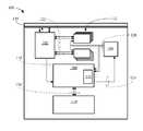
- the L2P table 302is organized having a one-directional logical-to-physical mapping to access the NVS memory 112 .
- the L2P table 302can have a structure that includes logical page numbers 304 , logical page entries 306 , logical-to-physical identifiers 308 , and a physical identifier length 312 .
- Each individual L2P page IDs 608 within one of the L2P partition offsets 604can be physically located by an offset from a starting location at the beginning of each of the L2P partition offsets 604 in a manner similar to the LP offsets 304 of FIG. 3 .
- each of the L2P partition offsets 604can be formed having the PIL 612 equal to 512-bytes and each of the L2P partition offsets 604 can have one hundred twenty eight L2P page IDs 608 on a 200 GB drive. It is understood that the L2P partition offsets 604 or the quantity of the L2P page IDs 608 can be changed, resulting a larger or smaller quantity of storage space needed in the volatile memory of the VM table 108 of FIG. 1 .
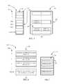
- FIG. 8therein is shown an example of a log super block page of one of the super log blocks 704 of FIG. 7 .
- the structure of the super log blocks 704can have a 1024-page size with 8 KB log pages having sixteen 512 byte sized partitions.
- Each of the super log blocks 704 of the L2P update log 702 of FIG. 7can have the same structure.
- the 8 KB log pagescan also be referred to as 8 KB_LPs 804 .
- the log super block page 802can be referred to as a L_SB page 802 .
- the L_SP page 802can contain up to sixteen 512-byte partitions. Each of the byte partitions can also be referred to as L2P partitions 806 .
- the 512-byte partitionscontain the actual data from the VM table 108 of FIG. 1 .
- L_SP page 802is written as a single atomic flash write.
- Metadata 808 stored with the L_SB page 802 of each of the 8 KB_LPs 804contains the partition numbers of the partitions stored in each of the L_SB page 802 .
- the metadata pages 812provides the flash layer or hardware of solid state storage devices the ability to quickly access the metadata 808 for rapid analysis, initialization, or rebuild of the VM table 108 of FIG. 1 on startup or for exception recovery.
- the main focus during initializationis to rebuild the L2P table 302 .
- the L2P table 302identifies the location of each partition in the flash, such as the L2P page IDs 608 .
- the L2P update log 702can be used to load the portion of the L2P table 302 first accessed before the entire L2P table 302 has been rebuilt to service host commands before the L2P table 302 has been fully loaded into the volatile memory table 108 or non-volatile memory.
- the memory controller 104determines the most recent version of each of the L2P partition 806 of FIG. 8 .
- the L2P table 302can be rebuilt by copying the most recent version of each partition into the appropriate location in the L2P table 302 .
- L2P update log 702is traversed to determine the most recent version of each of the L2P partition 806 of FIG. 8 .
- the super log blocks 704are identified in chronological order in the L2P update log 702 to permit reversed chronological ordering of the entries in the L2P update log 702 .
- the first entry in the reversed chronological ordercorresponds to the most recent version of the L2P update log 702 .
- a 420 GB drive with 1 KB partitions using the L2P update log 702 with a size equal to, five times greater than, or ten times greater than a size of the L2P table 302can have total initialization times of four hundred and thirty, six hundred and two, and eight hundred and seventeen milliseconds, respectively.
- the total initialization timesassume reads of the metadata pages 812 can be overlapped with writes to different flash devices, such as the NVS memory 112 of FIG. 1 and can change based on the read latency of the NAND flash.
- the metadata pages 812 of the super log blocks 704can be read and partition entries of the super log blocks 704 , such as partition entries, can be processed in parallel.
- the total initialization timesassume that writing the L2P table 302 will take no more than one microsecond and skipping an invalid entry will take no more than one hundred nanoseconds and can change based on the read latency of the NAND flash. For example, the total initialization times can improve as the read latency of NAND flash improves
- the L2P update log 702can represent the state from the last time a Page 63 has been written to one of the super log blocks 704 . Changes in the super log blocks 704 that are open do need to be captured because the L2P partitions 806 can be loaded and patched up as described earlier and can eliminate the need to capture all updates, such as changes in the super log blocks 704 that are not open, in the L2P update log 702 .
- the 8 KB_LPs 804 of FIG. 8are not mixed with host data pages in the same super block because of difficulties encountered when attempting to reclaim the super superblock.
- the larger the L2P update log 702the easier the recycling process. For example, a log ten times the size of a fully compact log has 1 valid partition for every 9 obsolete partitions.
- the worst caseis when the valid partitions are evenly distributed through the L2P update log 702 . In the worst case, there would be one valid partition on most the 8 KB_LPs 804 .
- the worst-case write amplification caused by the writes to the L2P update log 702are a function of the size of the L2P update log 702 .
- the L2P partitions 806 entries that are static and their associated logical pagescan be grouped together in the static log to prevent interspersion with the dynamic data and increasing the write amplification.
- the static datacan be marked as static and aggregated when moving a valid page during recycling.
- the write amplificationis at most 1 ⁇ 8 th . As described above, the write amplification is significantly less for large block or sequential operations. The write amplification associated with the recycle operations for a log ten times greater is at most one-eightieth when compared to the original host write of one-eighth.
- the recycle writes themselvescan trigger their own L2P log write and L2P log recycle writes, which can increase the write amplification for the writes by a maximum of one-eighth.
- L2P update log 702 with the super log blocks 704 for hosts writesenables large blocks of data to be kept together, aligned, or sequential and recycled to provide minimized write amplification by enabling writes to one or two partitions of NAND flash at a time, resulting in superior drive performance and reliability.
- the L2P partition table 1702is smaller than the logical-to-physical table 1708 and can be physically located in a portion of the VM table 108 of FIG. 1 or in separate volatile memory device.
- the L2P partition table 1702contains the location of each partition in the L2P log pages 1704 .
- the L2P log pages 1704can have a data structure similar to a data structure of the 8 KB_LPs 804 and have a size that is one-one hundred and twenty fourth the size of the logical-to-physical table 1708 .
- SSDsolid state drive
- a 1.2 TB SSDwould result in 1.2 GB of DDRAM for the logical-to-physical table 302 and if the 1.2 TB SSD has a maximum volatile memory size of 1 GB, the entire logical-to-physical table 302 would not fit in the RAM.
- the logical-to-physical partition tablecan be a supplemental (or replacement) table which points to the pieces of the L2P that are actually in RAM.
- the pieces of the L2P tablewould reside in a pooled area of RAM. At any one time, not all of the pieces of the L2P table are in memory, only a sparse number of pieces. Also, by not having all of the L2P table in memory at one time, the number of NAND flash reads required to start using the table will reduce the amount of start-up initialization time. It also means that only the segments of the L2P table in memory will have to be stored in the event of a power interruptions since the rest of the table already exists in the NAND.
- a large area of the volatile memory table 108 , of FIG. 1can be allocated to store a logical-to-physical pool (L2P pool).
- L2P poollogical-to-physical pool
- a L2P piece from the L2P poolcan be allocated and linked to the head of a most-recently-used list when reading a L2P partition from NAND.
- the L2P piececan be re-linked to the head of the MRU list.
- the oldest entries in the MRU listcan be reclaimed to the L2P pool.
- the traversal of the metadata 2204removes the need to back-fill the full L2P table.
- An estimated time for filling 480 MB of DDRAM using a DMAwould take at least 150 milliseconds.
- the traversal of the metadata 2204also removes need to read the entire L2P table, which is would require reading 480 MB from NAND flash and is estimated to take at least 600 milliseconds.
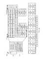
- the components of FIG. 23can be as follows—CH: Channel, 4 bits, 0 through 15; CE: Chip Enable, 2 bits, 0 through 3; LUN: Logical Unit, 1 bit, 0 or 1; EB: Erase Block, 13 bits, 0 through 4095; Page: Page number: 7 bits, 0 through 127; SP: Subpage, 1 bit, 0 or 1.
- the LUNcan be a die or portions of a die.
- the L2P IDs 308 of FIG. 3can include a portion of some or all of the components of FIG. 23 .
- the changes in the 100 GB L2P table 2402can be persistently captured and stored in non-volatile memory using logs in a manner similar to the L2P update log 702 of FIG. 7 , the super log blocks 704 of FIG. 7 , L2P partition table 1702 of FIG. 17 , or the L2P table 302 of FIG. 3 .
- the logscan be used to rebuild the 100 GB L2P table 2402 , structures, or data in volatile memory during a drive initialization, after a power cycle, or to restore any of the logs at any time
- L2P update log 2504is an example of a data structure in the NVM space 114 .
- the L2P update log 2504must be updated in a persistent manner to reflect any updates to the VM table 108 of FIG. 1 . Since the VM table 108 is modified whenever the location of a logical flash page is changed, updates to the NVM space 114 must be kept with modifications to the VM table 108 to enable the VM table 108 to be rebuilt across power cycles using the L2P update log 2504 in the NVM space 114 .
- the super log block 2604can have metadata of 32 bytes.
- the super log blocks 2604 of a L2P update log 114 of FIG. 1can be scattered throughout the drive and there is no restriction on the use of the super blocks.
- the super log blocks 704when in chronological order, form a sequential log. This sequential log is read only during drive initializations.
Landscapes
- Engineering & Computer Science (AREA)
- Theoretical Computer Science (AREA)
- Physics & Mathematics (AREA)
- General Engineering & Computer Science (AREA)
- General Physics & Mathematics (AREA)
- Techniques For Improving Reliability Of Storages (AREA)
Abstract
Description
Claims (10)
Priority Applications (1)
| Application Number | Priority Date | Filing Date | Title |
|---|---|---|---|
| US13/369,195US8909851B2 (en) | 2011-02-08 | 2012-02-08 | Storage control system with change logging mechanism and method of operation thereof |
Applications Claiming Priority (2)
| Application Number | Priority Date | Filing Date | Title |
|---|---|---|---|
| US201161440400P | 2011-02-08 | 2011-02-08 | |
| US13/369,195US8909851B2 (en) | 2011-02-08 | 2012-02-08 | Storage control system with change logging mechanism and method of operation thereof |
Publications (2)
| Publication Number | Publication Date |
|---|---|
| US20120203958A1 US20120203958A1 (en) | 2012-08-09 |
| US8909851B2true US8909851B2 (en) | 2014-12-09 |
Family
ID=46601466
Family Applications (1)
| Application Number | Title | Priority Date | Filing Date |
|---|---|---|---|
| US13/369,195Active2032-06-05US8909851B2 (en) | 2011-02-08 | 2012-02-08 | Storage control system with change logging mechanism and method of operation thereof |
Country Status (1)
| Country | Link |
|---|---|
| US (1) | US8909851B2 (en) |
Cited By (8)
| Publication number | Priority date | Publication date | Assignee | Title |
|---|---|---|---|---|
| EP3223160A1 (en) | 2016-03-21 | 2017-09-27 | Apple Inc. | Managing backup of logical-to-physical translation information to control boot-time and write amplification |
| US9940261B2 (en) | 2016-05-05 | 2018-04-10 | Western Digital Technology, Inc. | Zoning of logical to physical data address translation tables with parallelized log list replay |
| US20190294539A1 (en)* | 2018-03-23 | 2019-09-26 | Toshiba Memory Corporation | Memory system and method of controlling memory system |
| US10572391B2 (en) | 2018-02-09 | 2020-02-25 | Western Digital Technologies, Inc. | Methods and apparatus for implementing a logical to physical address mapping in a solid state drive |
| US10635331B2 (en) | 2017-07-05 | 2020-04-28 | Western Digital Technologies, Inc. | Distribution of logical-to-physical address entries across bank groups |
| US11487630B2 (en)* | 2019-01-08 | 2022-11-01 | Samsung Electronics Co., Ltd. | Storage device and data processing method thereof |
| WO2023196176A1 (en)* | 2022-04-05 | 2023-10-12 | Western Digital Technologies, Inc. | Storage optimization of cat table during background operations |
| US11874770B2 (en) | 2022-05-12 | 2024-01-16 | Western Digital Technologies, Inc. | Indexless logical-to-physical translation table |
Families Citing this family (67)
| Publication number | Priority date | Publication date | Assignee | Title |
|---|---|---|---|---|
| US9164679B2 (en) | 2011-04-06 | 2015-10-20 | Patents1, Llc | System, method and computer program product for multi-thread operation involving first memory of a first memory class and second memory of a second memory class |
| US9158546B1 (en) | 2011-04-06 | 2015-10-13 | P4tents1, LLC | Computer program product for fetching from a first physical memory between an execution of a plurality of threads associated with a second physical memory |
| US9176671B1 (en) | 2011-04-06 | 2015-11-03 | P4tents1, LLC | Fetching data between thread execution in a flash/DRAM/embedded DRAM-equipped system |
| US8930647B1 (en) | 2011-04-06 | 2015-01-06 | P4tents1, LLC | Multiple class memory systems |
| US9170744B1 (en) | 2011-04-06 | 2015-10-27 | P4tents1, LLC | Computer program product for controlling a flash/DRAM/embedded DRAM-equipped system |
| US9417754B2 (en) | 2011-08-05 | 2016-08-16 | P4tents1, LLC | User interface system, method, and computer program product |
| CN103488580A (en)* | 2012-06-14 | 2014-01-01 | 建兴电子科技股份有限公司 | Method for establishing address corresponding table of solid-state storage device |
| CN103970669A (en) | 2013-02-06 | 2014-08-06 | Lsi公司 | Method for accelerating physical-to-logic address mapping of recycling operation in solid-state equipment |
| US9454474B2 (en)* | 2013-03-05 | 2016-09-27 | Western Digital Technologies, Inc. | Methods, devices and systems for two stage power-on map rebuild with free space accounting in a solid state drive |
| US9612773B2 (en)* | 2013-11-21 | 2017-04-04 | Samsung Electronics Co., Ltd. | User device having a host flash translation layer (FTL), a method for transferring an erase count thereof, a method for transferring reprogram information thereof, and a method for transferring a page offset of an open block thereof |
| US20150149824A1 (en)* | 2013-11-25 | 2015-05-28 | Violin Memory Inc. | Method and apparatus for reconstructing an indirection table |
| TWI603194B (en)* | 2013-12-04 | 2017-10-21 | 慧榮科技股份有限公司 | Data storage device and data accessing method |
| US20150178164A1 (en)* | 2013-12-19 | 2015-06-25 | Violin Memory Inc. | Reconstructing an indirection table from logged media addresses |
| US10430092B1 (en)* | 2014-07-28 | 2019-10-01 | Rambus Inc. | Memory controller systems with nonvolatile memory for storing operating parameters |
| US10402092B2 (en)* | 2016-06-01 | 2019-09-03 | Western Digital Technologies, Inc. | Resizing namespaces for storage devices |
| US10564856B2 (en)* | 2017-07-06 | 2020-02-18 | Alibaba Group Holding Limited | Method and system for mitigating write amplification in a phase change memory-based storage device |
| US10628326B2 (en)* | 2017-08-21 | 2020-04-21 | Micron Technology, Inc. | Logical to physical mapping |
| CN111656330B (en) | 2017-12-21 | 2023-11-10 | 北极星特许集团有限责任公司 | NAND logical to physical table region tracking |
| JP6482690B1 (en)* | 2018-01-11 | 2019-03-13 | ウィンボンド エレクトロニクス コーポレーション | Semiconductor memory device |
| US10496548B2 (en) | 2018-02-07 | 2019-12-03 | Alibaba Group Holding Limited | Method and system for user-space storage I/O stack with user-space flash translation layer |
| US11379155B2 (en) | 2018-05-24 | 2022-07-05 | Alibaba Group Holding Limited | System and method for flash storage management using multiple open page stripes |
| CN111902804B (en) | 2018-06-25 | 2024-03-01 | 阿里巴巴集团控股有限公司 | System and method for managing resources of a storage device and quantifying I/O request costs |
| US10921992B2 (en) | 2018-06-25 | 2021-02-16 | Alibaba Group Holding Limited | Method and system for data placement in a hard disk drive based on access frequency for improved IOPS and utilization efficiency |
| US10996886B2 (en) | 2018-08-02 | 2021-05-04 | Alibaba Group Holding Limited | Method and system for facilitating atomicity and latency assurance on variable sized I/O |
| US10713163B2 (en) | 2018-09-11 | 2020-07-14 | Toshiba Memory Corporation | Set aware system data and mapping tables |
| US10909030B2 (en)* | 2018-09-11 | 2021-02-02 | Toshiba Memory Corporation | Enhanced trim command support for solid state drives |
| US11327929B2 (en) | 2018-09-17 | 2022-05-10 | Alibaba Group Holding Limited | Method and system for reduced data movement compression using in-storage computing and a customized file system |
| US10977122B2 (en) | 2018-12-31 | 2021-04-13 | Alibaba Group Holding Limited | System and method for facilitating differentiated error correction in high-density flash devices |
| US11061735B2 (en) | 2019-01-02 | 2021-07-13 | Alibaba Group Holding Limited | System and method for offloading computation to storage nodes in distributed system |
| US11132291B2 (en) | 2019-01-04 | 2021-09-28 | Alibaba Group Holding Limited | System and method of FPGA-executed flash translation layer in multiple solid state drives |
| US11301369B2 (en) | 2019-01-24 | 2022-04-12 | Western Digital Technologies, Inc. | Logical to physical mapping management using low-latency non-volatile memory |
| US11200337B2 (en) | 2019-02-11 | 2021-12-14 | Alibaba Group Holding Limited | System and method for user data isolation |
| US10922234B2 (en)* | 2019-04-11 | 2021-02-16 | Alibaba Group Holding Limited | Method and system for online recovery of logical-to-physical mapping table affected by noise sources in a solid state drive |
| KR102815137B1 (en)* | 2019-06-25 | 2025-06-02 | 에스케이하이닉스 주식회사 | Memory system |
| US10860223B1 (en) | 2019-07-18 | 2020-12-08 | Alibaba Group Holding Limited | Method and system for enhancing a distributed storage system by decoupling computation and network tasks |
| US11617282B2 (en) | 2019-10-01 | 2023-03-28 | Alibaba Group Holding Limited | System and method for reshaping power budget of cabinet to facilitate improved deployment density of servers |
| US11126561B2 (en) | 2019-10-01 | 2021-09-21 | Alibaba Group Holding Limited | Method and system for organizing NAND blocks and placing data to facilitate high-throughput for random writes in a solid state drive |
| US11449455B2 (en) | 2020-01-15 | 2022-09-20 | Alibaba Group Holding Limited | Method and system for facilitating a high-capacity object storage system with configuration agility and mixed deployment flexibility |
| US11379447B2 (en) | 2020-02-06 | 2022-07-05 | Alibaba Group Holding Limited | Method and system for enhancing IOPS of a hard disk drive system based on storing metadata in host volatile memory and data in non-volatile memory using a shared controller |
| US11150986B2 (en) | 2020-02-26 | 2021-10-19 | Alibaba Group Holding Limited | Efficient compaction on log-structured distributed file system using erasure coding for resource consumption reduction |
| US11200114B2 (en) | 2020-03-17 | 2021-12-14 | Alibaba Group Holding Limited | System and method for facilitating elastic error correction code in memory |
| US11449386B2 (en) | 2020-03-20 | 2022-09-20 | Alibaba Group Holding Limited | Method and system for optimizing persistent memory on data retention, endurance, and performance for host memory |
| US11169881B2 (en) | 2020-03-30 | 2021-11-09 | Alibaba Group Holding Limited | System and method for facilitating reduction of complexity and data movement in erasure coding merging on journal and data storage drive |
| US11385833B2 (en) | 2020-04-20 | 2022-07-12 | Alibaba Group Holding Limited | Method and system for facilitating a light-weight garbage collection with a reduced utilization of resources |
| US11301173B2 (en) | 2020-04-20 | 2022-04-12 | Alibaba Group Holding Limited | Method and system for facilitating evaluation of data access frequency and allocation of storage device resources |
| US11281575B2 (en) | 2020-05-11 | 2022-03-22 | Alibaba Group Holding Limited | Method and system for facilitating data placement and control of physical addresses with multi-queue I/O blocks |
| US11461262B2 (en) | 2020-05-13 | 2022-10-04 | Alibaba Group Holding Limited | Method and system for facilitating a converged computation and storage node in a distributed storage system |
| US11494115B2 (en) | 2020-05-13 | 2022-11-08 | Alibaba Group Holding Limited | System method for facilitating memory media as file storage device based on real-time hashing by performing integrity check with a cyclical redundancy check (CRC) |
| US11218165B2 (en) | 2020-05-15 | 2022-01-04 | Alibaba Group Holding Limited | Memory-mapped two-dimensional error correction code for multi-bit error tolerance in DRAM |
| US11507499B2 (en) | 2020-05-19 | 2022-11-22 | Alibaba Group Holding Limited | System and method for facilitating mitigation of read/write amplification in data compression |
| US11556277B2 (en) | 2020-05-19 | 2023-01-17 | Alibaba Group Holding Limited | System and method for facilitating improved performance in ordering key-value storage with input/output stack simplification |
| US11436153B2 (en)* | 2020-05-26 | 2022-09-06 | Western Digital Technologies, Inc. | Moving change log tables to align to zones |
| US11263132B2 (en) | 2020-06-11 | 2022-03-01 | Alibaba Group Holding Limited | Method and system for facilitating log-structure data organization |
| US11354200B2 (en) | 2020-06-17 | 2022-06-07 | Alibaba Group Holding Limited | Method and system for facilitating data recovery and version rollback in a storage device |
| US11422931B2 (en) | 2020-06-17 | 2022-08-23 | Alibaba Group Holding Limited | Method and system for facilitating a physically isolated storage unit for multi-tenancy virtualization |
| US11354233B2 (en) | 2020-07-27 | 2022-06-07 | Alibaba Group Holding Limited | Method and system for facilitating fast crash recovery in a storage device |
| US11379141B2 (en)* | 2020-07-31 | 2022-07-05 | Kioxia Corporation | SSD supporting read-only mode after PLP backup failure |
| US11372774B2 (en) | 2020-08-24 | 2022-06-28 | Alibaba Group Holding Limited | Method and system for a solid state drive with on-chip memory integration |
| US11487465B2 (en) | 2020-12-11 | 2022-11-01 | Alibaba Group Holding Limited | Method and system for a local storage engine collaborating with a solid state drive controller |
| US11734115B2 (en) | 2020-12-28 | 2023-08-22 | Alibaba Group Holding Limited | Method and system for facilitating write latency reduction in a queue depth of one scenario |
| US11416365B2 (en) | 2020-12-30 | 2022-08-16 | Alibaba Group Holding Limited | Method and system for open NAND block detection and correction in an open-channel SSD |
| KR20220130389A (en)* | 2021-03-18 | 2022-09-27 | 에스케이하이닉스 주식회사 | A memory system and method of operation of the memory system |
| US11726699B2 (en) | 2021-03-30 | 2023-08-15 | Alibaba Singapore Holding Private Limited | Method and system for facilitating multi-stream sequential read performance improvement with reduced read amplification |
| US11461173B1 (en) | 2021-04-21 | 2022-10-04 | Alibaba Singapore Holding Private Limited | Method and system for facilitating efficient data compression based on error correction code and reorganization of data placement |
| US11476874B1 (en) | 2021-05-14 | 2022-10-18 | Alibaba Singapore Holding Private Limited | Method and system for facilitating a storage server with hybrid memory for journaling and data storage |
| US11995085B2 (en)* | 2022-02-25 | 2024-05-28 | Visa International Service Association | System, method, and computer program product for efficiently storing multi-threaded log data |
| US12038848B1 (en)* | 2023-03-28 | 2024-07-16 | Sk Hynix Nand Product Solutions Corp. | Compression of logical-to-physical address indirection table on solid-state drives |
Citations (146)
| Publication number | Priority date | Publication date | Assignee | Title |
|---|---|---|---|---|
| US4048481A (en) | 1974-12-17 | 1977-09-13 | Honeywell Information Systems Inc. | Diagnostic testing apparatus and method |
| US5311395A (en) | 1992-10-29 | 1994-05-10 | Ncr Corporation | Surface mount heat sink |
| US5479638A (en) | 1993-03-26 | 1995-12-26 | Cirrus Logic, Inc. | Flash memory mass storage architecture incorporation wear leveling technique |
| US5930504A (en) | 1996-07-22 | 1999-07-27 | Intel Corporation | Dynamic nonvolatile memory update in a computer system |
| US5949785A (en) | 1995-11-01 | 1999-09-07 | Whittaker Corporation | Network access communications system and methodology |
| US5963983A (en) | 1996-04-15 | 1999-10-05 | International Business Machines Corporation | Method and apparatus for dynamically creating conversion tables to access a semiconductor memory device |
| US6091652A (en) | 1998-12-11 | 2000-07-18 | Lsi Logic Corporation | Testing semiconductor devices for data retention |
| US6275436B1 (en) | 1993-04-08 | 2001-08-14 | Hitachi, Ltd | Flash memory control method and apparatus processing system therewith |
| US6345367B1 (en) | 1996-07-11 | 2002-02-05 | Memory Corporation Plc | Defective memory block handling system by addressing a group of memory blocks for erasure and changing the content therewith |
| US6356447B2 (en) | 2000-06-20 | 2002-03-12 | Adc Telecommunications, Inc. | Surface mounted conduction heat sink |
| US6381670B1 (en) | 1997-01-07 | 2002-04-30 | Aplus Flash Technology, Inc. | Flash memory array having maximum and minimum threshold voltage detection for eliminating over-erasure problem and enhancing write operation |
| US6412080B1 (en) | 1999-02-23 | 2002-06-25 | Microsoft Corporation | Lightweight persistent storage system for flash memory devices |
| US20020159285A1 (en) | 2000-03-01 | 2002-10-31 | Stephen Morley | Data balancing scheme in solid state storage devices |
| US20030046603A1 (en) | 1989-04-13 | 2003-03-06 | Eliyahou Harari | Flash EEprom system |
| US20030074592A1 (en) | 2001-10-15 | 2003-04-17 | Fujitsu Limited | Information processing apparatus, power supply control method for plural information processing apparatuses, and storage medium therefore |
| US6552581B1 (en) | 2000-08-25 | 2003-04-22 | Agere Systems Inc. | Current recycling circuit and a method of current recycling |
| US6587915B1 (en) | 1999-09-29 | 2003-07-01 | Samsung Electronics Co., Ltd. | Flash memory having data blocks, spare blocks, a map block and a header block and a method for controlling the same |
| US20030163633A1 (en) | 2002-02-27 | 2003-08-28 | Aasheim Jered Donald | System and method for achieving uniform wear levels in a flash memory device |
| US6618249B2 (en) | 2002-02-05 | 2003-09-09 | Quantum Corporation | Thermal cooling system for densely packed storage devices |
| US6728913B1 (en) | 2000-02-25 | 2004-04-27 | Advanced Micro Devices, Inc. | Data recycling in memory |
| US20040080985A1 (en) | 2002-10-28 | 2004-04-29 | Sandisk Corporation, A Delaware Corporation | Maintaining erase counts in non-volatile storage systems |
| US6763424B2 (en) | 2001-01-19 | 2004-07-13 | Sandisk Corporation | Partial block data programming and reading operations in a non-volatile memory |
| US6775792B2 (en) | 2001-01-29 | 2004-08-10 | Snap Appliance, Inc. | Discrete mapping of parity blocks |
| US20040252670A1 (en) | 2003-06-12 | 2004-12-16 | Nokia Corporation | Adaptive power margin adjustment for a 1xEV-DV system |
| US20050021904A1 (en) | 2003-06-05 | 2005-01-27 | Stmicroelectronics S.R.L. | Mass memory device based on a flash memory with multiple buffers |
| US6850443B2 (en) | 1991-09-13 | 2005-02-01 | Sandisk Corporation | Wear leveling techniques for flash EEPROM systems |
| US6854070B2 (en) | 2000-01-25 | 2005-02-08 | Hewlett-Packard Development Company, L.P. | Hot-upgrade/hot-add memory |
| US20050038792A1 (en) | 2003-08-14 | 2005-02-17 | Johnson Ted C. | Apparatus and method for operating circular files |
| US20050073884A1 (en) | 2003-10-03 | 2005-04-07 | Gonzalez Carlos J. | Flash memory data correction and scrub techniques |
| US6903972B2 (en) | 2003-07-30 | 2005-06-07 | M-Systems Flash Disk Pioneers Ltd. | Different methods applied for archiving data according to their desired lifetime |
| US6906961B2 (en) | 2003-06-24 | 2005-06-14 | Micron Technology, Inc. | Erase block data splitting |
| US6975028B1 (en) | 2003-03-19 | 2005-12-13 | Delta Design, Inc. | Thermal apparatus for engaging electronic device |
| US20060020745A1 (en) | 2004-07-21 | 2006-01-26 | Conley Kevin M | Fat analysis for optimized sequential cluster management |
| US20060136682A1 (en) | 2004-12-21 | 2006-06-22 | Sriram Haridas | Method and apparatus for arbitrarily initializing a portion of memory |
| US20060143365A1 (en) | 2002-06-19 | 2006-06-29 | Tokyo Electron Device Limited | Memory device, memory managing method and program |
| US7082495B2 (en) | 2002-06-27 | 2006-07-25 | Microsoft Corporation | Method and apparatus to reduce power consumption and improve read/write performance of hard disk drives using non-volatile memory |
| US7107389B2 (en) | 2002-08-29 | 2006-09-12 | Matsushita Electric Industrial Co., Ltd. | Semiconductor memory device and method for writing data into flash memory |
| US20060253641A1 (en) | 2003-08-07 | 2006-11-09 | Micron Technology, Inc. | Multiple erase block tagging in a flash memory device |
| US7139864B2 (en) | 2003-12-30 | 2006-11-21 | Sandisk Corporation | Non-volatile memory and method with block management system |
| US20060282644A1 (en) | 2005-06-08 | 2006-12-14 | Micron Technology, Inc. | Robust index storage for non-volatile memory |
| US20060294574A1 (en) | 2005-06-22 | 2006-12-28 | Cha Sang H | Apparatuses and methods for receiving software/firmware |
| US20070061511A1 (en) | 2005-09-15 | 2007-03-15 | Faber Robert W | Distributed and packed metadata structure for disk cache |
| US20070083779A1 (en) | 2005-10-07 | 2007-04-12 | Renesas Technology Corp. | Semiconductor integrated circuit device and power consumption control device |
| US7233497B2 (en) | 2004-10-06 | 2007-06-19 | Hewlett-Packard Development Company, L.P. | Surface mount heat sink |
| US7243186B2 (en) | 2003-12-22 | 2007-07-10 | Phison Electronics Corp. | Method of optimizing performance of flash memory |
| US20070234004A1 (en) | 2006-03-31 | 2007-10-04 | Takashi Oshima | Memory system and controller |
| US20070260811A1 (en) | 2006-05-08 | 2007-11-08 | Merry David E Jr | Systems and methods for measuring the useful life of solid-state storage devices |
| US20070263444A1 (en) | 2006-05-15 | 2007-11-15 | Gorobets Sergey A | Non-Volatile Memory System with End of Life Calculation |
| US20070276973A1 (en) | 2004-09-30 | 2007-11-29 | Intel Corporation | Managing queues |
| US7330927B1 (en) | 2003-05-07 | 2008-02-12 | Avago Technologies General Ip (Singapore) Pte. Ltd. | Apparatus and methodology for a pointer manager |
| US7333364B2 (en) | 2000-01-06 | 2008-02-19 | Super Talent Electronics, Inc. | Cell-downgrading and reference-voltage adjustment for a multi-bit-cell flash memory |
| US20080046630A1 (en) | 2006-08-21 | 2008-02-21 | Sandisk Il Ltd. | NAND flash memory controller exporting a logical sector-based interface |
| US20080052446A1 (en) | 2006-08-28 | 2008-02-28 | Sandisk Il Ltd. | Logical super block mapping for NAND flash memory |
| US20080082736A1 (en) | 2004-03-11 | 2008-04-03 | Chow David Q | Managing bad blocks in various flash memory cells for electronic data flash card |
| US7355896B2 (en) | 2005-12-22 | 2008-04-08 | Chartered Semiconductor Manufacturing Ltd. | System for improving endurance and data retention in memory devices |
| US20080183918A1 (en) | 2007-01-31 | 2008-07-31 | Microsoft Corporation | Extending flash drive lifespan |
| US7434122B2 (en) | 2004-08-04 | 2008-10-07 | Samsung Electronics Co., Ltd. | Flash memory device for performing bad block management and method of performing bad block management of flash memory device |
| US7441067B2 (en) | 2004-11-15 | 2008-10-21 | Sandisk Corporation | Cyclic flash memory wear leveling |
| EP1990921A2 (en) | 2007-05-07 | 2008-11-12 | Broadcom Corporation | Operational parameter adaptable LDPC (low density parity check) decoder |
| US20080313505A1 (en) | 2007-06-14 | 2008-12-18 | Samsung Electronics Co., Ltd. | Flash memory wear-leveling |
| US20090019321A1 (en) | 2007-07-09 | 2009-01-15 | Micron Technolgy. Inc. | Error correction for memory |
| US20090089485A1 (en) | 2007-09-27 | 2009-04-02 | Phison Electronics Corp. | Wear leveling method and controller using the same |
| US7516267B2 (en)* | 2005-11-03 | 2009-04-07 | Intel Corporation | Recovering from a non-volatile memory failure |
| US20090138654A1 (en) | 2006-12-11 | 2009-05-28 | Pantas Sutardja | Fatigue management system and method for hybrid nonvolatile solid state memory system |
| US20090157948A1 (en) | 2007-12-14 | 2009-06-18 | Spansion Llc | Intelligent memory data management |
| US20090164702A1 (en) | 2007-12-21 | 2009-06-25 | Spansion Llc | Frequency distributed flash memory allocation based on free page tables |
| US20090172262A1 (en) | 2007-12-27 | 2009-07-02 | Pliant Technology, Inc. | Metadata rebuild in a flash memory controller following a loss of power |
| US20090228761A1 (en) | 2008-03-07 | 2009-09-10 | Anobit Technologies Ltd | Efficient readout from analog memory cells using data compression |
| US20090259819A1 (en) | 2008-04-09 | 2009-10-15 | Skymedi Corporation | Method of wear leveling for non-volatile memory |
| US20090259896A1 (en) | 2008-04-10 | 2009-10-15 | Phison Electronics Corp. | Bad block identifying method for flash memory, storage system, and controller thereof |
| US7613871B2 (en) | 2005-06-21 | 2009-11-03 | Hitachi, Ltd. | Storage system using a flash memory partitioned with write-once and rewritable blocks |
| US7620769B2 (en) | 2000-01-06 | 2009-11-17 | Super Talent Electronics, Inc. | Recycling partially-stale flash blocks using a sliding window for multi-level-cell (MLC) flash memory |
| US7639532B2 (en) | 2007-10-10 | 2009-12-29 | Micron Technology, Inc. | Non-equal threshold voltage ranges in MLC NAND |
| US20090327591A1 (en) | 2008-06-25 | 2009-12-31 | Stec, Inc. | Slc-mlc combination flash storage device |
| US20090327581A1 (en) | 2008-06-30 | 2009-12-31 | Coulson Richard L | Nand memory |
| US20090323419A1 (en) | 2008-06-26 | 2009-12-31 | Sdc Micro Inc. | Read-time wear-leveling method in storage system using flash memory device |
| US20100017650A1 (en) | 2008-07-19 | 2010-01-21 | Nanostar Corporation, U.S.A | Non-volatile memory data storage system with reliability management |
| US20100023674A1 (en) | 2008-07-28 | 2010-01-28 | Aviles Joaquin J | Flash DIMM in a Standalone Cache Appliance System and Methodology |
| US7661054B2 (en) | 2005-09-30 | 2010-02-09 | Intel Corporation | Methods and arrangements to remap degraded storage blocks |
| US20100050053A1 (en) | 2008-08-22 | 2010-02-25 | Wilson Bruce A | Error control in a flash memory device |
| US7679948B2 (en) | 2008-06-05 | 2010-03-16 | Sun Microsystems, Inc. | Write and read assist circuit for SRAM with power recycling |
| US20100138592A1 (en)* | 2008-12-02 | 2010-06-03 | Samsung Electronics Co. Ltd. | Memory device, memory system and mapping information recovering method |
| US7738502B2 (en) | 2006-09-01 | 2010-06-15 | Intel Corporation | Signal noise filtering in a serial interface |
| US7743216B2 (en) | 2006-06-30 | 2010-06-22 | Seagate Technology Llc | Predicting accesses to non-requested data |
| US20100169541A1 (en) | 2008-12-30 | 2010-07-01 | Guy Freikorn | Method and apparatus for retroactive adaptation of data location |
| US20100174845A1 (en) | 2009-01-05 | 2010-07-08 | Sergey Anatolievich Gorobets | Wear Leveling for Non-Volatile Memories: Maintenance of Experience Count and Passive Techniques |
| US20100217915A1 (en) | 2009-02-23 | 2010-08-26 | International Business Machines Corporation | High availability memory system |
| US20100262795A1 (en) | 2009-04-08 | 2010-10-14 | Steven Robert Hetzler | System, method, and computer program product for analyzing monitor data information from a plurality of memory devices having finite endurance and/or retention |
| US20100262875A1 (en) | 2009-04-08 | 2010-10-14 | Steven Robert Hetzler | System, method, and computer program product for determining a retention behavior for at least one block of a memory device having finite endurance and/or retention |
| US20100262792A1 (en) | 2009-04-08 | 2010-10-14 | Steven Robert Hetzler | System, method, and computer program product for estimating when a reliable life of a memory device having finite endurance and/or retention, or portion thereof, will be expended |
| US7818525B1 (en) | 2009-08-12 | 2010-10-19 | Texas Memory Systems, Inc. | Efficient reduction of read disturb errors in NAND FLASH memory |
| US7827348B2 (en) | 2000-01-06 | 2010-11-02 | Super Talent Electronics, Inc. | High performance flash memory devices (FMD) |
| US7830164B2 (en) | 2008-04-22 | 2010-11-09 | Honeywell International Inc. | Ducted test socket |
| US20100287328A1 (en) | 2009-05-07 | 2010-11-11 | Seagate Technology Llc | Wear leveling technique for storage devices |
| US20100293367A1 (en) | 2009-05-13 | 2010-11-18 | Dell Products L.P. | System and Method for Optimizing Performance of an Information Handling System Component |
| US20100312954A1 (en) | 2007-04-27 | 2010-12-09 | Byung-Gil Jeon | Multi-Chip Semiconductor Devices Having Non-Volatile Memory Devices Therein |
| US20100318719A1 (en) | 2009-06-12 | 2010-12-16 | Micron Technology, Inc. | Methods, memory controllers and devices for wear leveling a memory |
| US20100332726A1 (en) | 2009-06-26 | 2010-12-30 | Solid State System Co., Ltd. | Structure and method for managing writing operation on mlc flash memory |
| US20110066788A1 (en) | 2009-09-15 | 2011-03-17 | International Business Machines Corporation | Container marker scheme for reducing write amplification in solid state devices |
| US20110131447A1 (en) | 2009-11-30 | 2011-06-02 | Gyan Prakash | Automated modular and secure boot firmware update |
| US20110131365A1 (en)* | 2009-11-30 | 2011-06-02 | Via Technologies, Inc. | Data Storage System and Method |
| US20110145473A1 (en) | 2009-12-11 | 2011-06-16 | Nimble Storage, Inc. | Flash Memory Cache for Data Storage Device |
| US7979614B1 (en) | 2005-05-05 | 2011-07-12 | Marvell International Ltd. | Flash memory/disk drive interface and method for same |
| US20110191522A1 (en) | 2010-02-02 | 2011-08-04 | Condict Michael N | Managing Metadata and Page Replacement in a Persistent Cache in Flash Memory |
| US20110191649A1 (en) | 2010-02-01 | 2011-08-04 | Samsung Electronics Co., Ltd. | Solid state drive and method of controlling an error thereof |
| US20110190963A1 (en) | 2010-01-29 | 2011-08-04 | Eurocopter Deutschland Gmbh | Method and system for an optimized utilization of energy resources of an electrical system |
| US8001135B2 (en) | 2007-03-02 | 2011-08-16 | Kabushiki Kaisha Toshiba | Search support apparatus, computer program product, and search support system |
| US8010738B1 (en) | 2008-06-27 | 2011-08-30 | Emc Corporation | Techniques for obtaining a specified lifetime for a data storage device |
| US8028123B2 (en) | 2008-04-15 | 2011-09-27 | SMART Modular Technologies (AZ) , Inc. | Circular wear leveling |
| US20110238892A1 (en) | 2010-03-24 | 2011-09-29 | Lite-On It Corp. | Wear leveling method of non-volatile memory |
| US8072805B2 (en) | 2009-08-18 | 2011-12-06 | Skymedi Corporation | Method and system of finding a read voltage for a flash memory |
| US20110320687A1 (en) | 2010-06-29 | 2011-12-29 | International Business Machines Corporation | Reducing write amplification in a cache with flash memory used as a write cache |
| US8095724B2 (en) | 2008-02-05 | 2012-01-10 | Skymedi Corporation | Method of wear leveling for non-volatile memory and apparatus using via shifting windows |
| US8095765B2 (en) | 2009-03-04 | 2012-01-10 | Micron Technology, Inc. | Memory block management |
| US8117396B1 (en) | 2006-10-10 | 2012-02-14 | Network Appliance, Inc. | Multi-level buffer cache management through soft-division of a uniform buffer cache |
| US20120047409A1 (en) | 2010-08-23 | 2012-02-23 | Apple Inc. | Systems and methods for generating dynamic super blocks |
| US20120047320A1 (en) | 2010-08-20 | 2012-02-23 | Samsung Electronics Co., Ltd | Method and apparatus to interface semiconductor storage device and host to provide performance throttling of semiconductor storage device |
| US8127202B2 (en) | 2006-05-15 | 2012-02-28 | Apple Inc. | Use of alternative value in cell detection |
| US8145984B2 (en) | 2006-10-30 | 2012-03-27 | Anobit Technologies Ltd. | Reading memory cells using multiple thresholds |
| US8154921B2 (en) | 2008-05-09 | 2012-04-10 | Sandisk Technologies Inc. | Dynamic and adaptive optimization of read compare levels based on memory cell threshold voltage distribution |
| US8169825B1 (en) | 2008-09-02 | 2012-05-01 | Anobit Technologies Ltd. | Reliable data storage in analog memory cells subjected to long retention periods |
| US20120124046A1 (en) | 2010-11-16 | 2012-05-17 | Actifio, Inc. | System and method for managing deduplicated copies of data using temporal relationships among copies |
| US20120124273A1 (en) | 2010-11-12 | 2012-05-17 | Seagate Technology Llc | Estimating Wear of Non-Volatile, Solid State Memory |
| US20120151260A1 (en) | 2010-12-08 | 2012-06-14 | Arnaldo Zimmermann | System and Method for Autonomous NAND Refresh |
| US8219724B1 (en) | 2010-09-29 | 2012-07-10 | Emc Corporation | Flexibly managing I/O operations based on application awareness |
| US8219776B2 (en) | 2009-09-23 | 2012-07-10 | Lsi Corporation | Logical-to-physical address translation for solid state disks |
| US8228701B2 (en) | 2009-03-01 | 2012-07-24 | Apple Inc. | Selective activation of programming schemes in analog memory cell arrays |
| US20120216085A1 (en) | 2011-02-23 | 2012-08-23 | Densbits Technologies Ltd. | Devices and method for wear estimation based memory management |
| US8254172B1 (en) | 2009-09-30 | 2012-08-28 | Western Digital Technologies, Inc. | Wear leveling non-volatile semiconductor memory based on erase times and program times |
| US8259506B1 (en) | 2009-03-25 | 2012-09-04 | Apple Inc. | Database of memory read thresholds |
| US20120239858A1 (en) | 2010-07-07 | 2012-09-20 | Stec, Inc. | Apparatus and method for determining an operating condition of a memory cell based on cycle information |
| US8289801B2 (en) | 2009-09-09 | 2012-10-16 | Fusion-Io, Inc. | Apparatus, system, and method for power reduction management in a storage device |
| US20120266048A1 (en) | 2011-04-15 | 2012-10-18 | Chun Sing Jackson Chung | Dynamic Optimization of Back-End Memory System Interface |
| US8332578B2 (en) | 2009-07-31 | 2012-12-11 | Intel Corporation | Method and system to improve the performance of a multi-level cell (MLC) NAND flash memory |
| US20120331207A1 (en) | 2011-06-24 | 2012-12-27 | Lassa Paul A | Controller, Storage Device, and Method for Power Throttling Memory Operations |
| US20130007380A1 (en) | 2011-06-30 | 2013-01-03 | Seagate Technology Llc | Limiting activity rates that impact life of a data storage media |
| US8363413B2 (en) | 2010-09-13 | 2013-01-29 | Raytheon Company | Assembly to provide thermal cooling |
| US8369141B2 (en) | 2007-03-12 | 2013-02-05 | Apple Inc. | Adaptive estimation of memory cell read thresholds |
| US20130073788A1 (en) | 2011-09-16 | 2013-03-21 | Apple Inc. | Weave sequence counter for non-volatile memory systems |
| US8407409B2 (en) | 2009-04-02 | 2013-03-26 | Hitachi, Ltd. | Metrics and management for flash memory storage life |
| US20130080691A1 (en) | 2007-12-05 | 2013-03-28 | Hanan Weingarten | Flash memory device with physical cell value deterioration accommodation and methods useful in conjunction therewith |
| US20130100600A1 (en) | 2011-10-19 | 2013-04-25 | Hon Hai Precision Industry Co., Ltd. | Computer system with airflow guiding duct |
| US20130124792A1 (en) | 2011-02-03 | 2013-05-16 | Stec, Inc. | Erase-suspend system and method |
| US8464106B2 (en) | 2009-08-24 | 2013-06-11 | Ocz Technology Group, Inc. | Computer system with backup function and method therefor |
| US8612804B1 (en) | 2010-09-30 | 2013-12-17 | Western Digital Technologies, Inc. | System and method for improving wear-leveling performance in solid-state memory |
| US20140108891A1 (en) | 2010-01-27 | 2014-04-17 | Fusion-Io, Inc. | Managing non-volatile media |
- 2012
- 2012-02-08USUS13/369,195patent/US8909851B2/enactiveActive
Patent Citations (153)
| Publication number | Priority date | Publication date | Assignee | Title |
|---|---|---|---|---|
| US4048481A (en) | 1974-12-17 | 1977-09-13 | Honeywell Information Systems Inc. | Diagnostic testing apparatus and method |
| US20030046603A1 (en) | 1989-04-13 | 2003-03-06 | Eliyahou Harari | Flash EEprom system |
| US6850443B2 (en) | 1991-09-13 | 2005-02-01 | Sandisk Corporation | Wear leveling techniques for flash EEPROM systems |
| US5311395A (en) | 1992-10-29 | 1994-05-10 | Ncr Corporation | Surface mount heat sink |
| US5479638A (en) | 1993-03-26 | 1995-12-26 | Cirrus Logic, Inc. | Flash memory mass storage architecture incorporation wear leveling technique |
| US6275436B1 (en) | 1993-04-08 | 2001-08-14 | Hitachi, Ltd | Flash memory control method and apparatus processing system therewith |
| US5949785A (en) | 1995-11-01 | 1999-09-07 | Whittaker Corporation | Network access communications system and methodology |
| US5963983A (en) | 1996-04-15 | 1999-10-05 | International Business Machines Corporation | Method and apparatus for dynamically creating conversion tables to access a semiconductor memory device |
| US6345367B1 (en) | 1996-07-11 | 2002-02-05 | Memory Corporation Plc | Defective memory block handling system by addressing a group of memory blocks for erasure and changing the content therewith |
| US5930504A (en) | 1996-07-22 | 1999-07-27 | Intel Corporation | Dynamic nonvolatile memory update in a computer system |
| US6381670B1 (en) | 1997-01-07 | 2002-04-30 | Aplus Flash Technology, Inc. | Flash memory array having maximum and minimum threshold voltage detection for eliminating over-erasure problem and enhancing write operation |
| US6091652A (en) | 1998-12-11 | 2000-07-18 | Lsi Logic Corporation | Testing semiconductor devices for data retention |
| US6412080B1 (en) | 1999-02-23 | 2002-06-25 | Microsoft Corporation | Lightweight persistent storage system for flash memory devices |
| US6587915B1 (en) | 1999-09-29 | 2003-07-01 | Samsung Electronics Co., Ltd. | Flash memory having data blocks, spare blocks, a map block and a header block and a method for controlling the same |
| US7333364B2 (en) | 2000-01-06 | 2008-02-19 | Super Talent Electronics, Inc. | Cell-downgrading and reference-voltage adjustment for a multi-bit-cell flash memory |
| US7620769B2 (en) | 2000-01-06 | 2009-11-17 | Super Talent Electronics, Inc. | Recycling partially-stale flash blocks using a sliding window for multi-level-cell (MLC) flash memory |
| US7827348B2 (en) | 2000-01-06 | 2010-11-02 | Super Talent Electronics, Inc. | High performance flash memory devices (FMD) |
| US6854070B2 (en) | 2000-01-25 | 2005-02-08 | Hewlett-Packard Development Company, L.P. | Hot-upgrade/hot-add memory |
| US6728913B1 (en) | 2000-02-25 | 2004-04-27 | Advanced Micro Devices, Inc. | Data recycling in memory |
| US20020159285A1 (en) | 2000-03-01 | 2002-10-31 | Stephen Morley | Data balancing scheme in solid state storage devices |
| US6356447B2 (en) | 2000-06-20 | 2002-03-12 | Adc Telecommunications, Inc. | Surface mounted conduction heat sink |
| US6552581B1 (en) | 2000-08-25 | 2003-04-22 | Agere Systems Inc. | Current recycling circuit and a method of current recycling |
| US6763424B2 (en) | 2001-01-19 | 2004-07-13 | Sandisk Corporation | Partial block data programming and reading operations in a non-volatile memory |
| US6775792B2 (en) | 2001-01-29 | 2004-08-10 | Snap Appliance, Inc. | Discrete mapping of parity blocks |
| US20030074592A1 (en) | 2001-10-15 | 2003-04-17 | Fujitsu Limited | Information processing apparatus, power supply control method for plural information processing apparatuses, and storage medium therefore |
| US6778387B2 (en) | 2002-02-05 | 2004-08-17 | Quantum Corporation | Thermal cooling system for densely packed storage devices |
| US6618249B2 (en) | 2002-02-05 | 2003-09-09 | Quantum Corporation | Thermal cooling system for densely packed storage devices |
| US20030163633A1 (en) | 2002-02-27 | 2003-08-28 | Aasheim Jered Donald | System and method for achieving uniform wear levels in a flash memory device |
| US20060143365A1 (en) | 2002-06-19 | 2006-06-29 | Tokyo Electron Device Limited | Memory device, memory managing method and program |
| US7082495B2 (en) | 2002-06-27 | 2006-07-25 | Microsoft Corporation | Method and apparatus to reduce power consumption and improve read/write performance of hard disk drives using non-volatile memory |
| US7107389B2 (en) | 2002-08-29 | 2006-09-12 | Matsushita Electric Industrial Co., Ltd. | Semiconductor memory device and method for writing data into flash memory |
| US20040080985A1 (en) | 2002-10-28 | 2004-04-29 | Sandisk Corporation, A Delaware Corporation | Maintaining erase counts in non-volatile storage systems |
| US6975028B1 (en) | 2003-03-19 | 2005-12-13 | Delta Design, Inc. | Thermal apparatus for engaging electronic device |
| US7330927B1 (en) | 2003-05-07 | 2008-02-12 | Avago Technologies General Ip (Singapore) Pte. Ltd. | Apparatus and methodology for a pointer manager |
| US20050021904A1 (en) | 2003-06-05 | 2005-01-27 | Stmicroelectronics S.R.L. | Mass memory device based on a flash memory with multiple buffers |
| US20040252670A1 (en) | 2003-06-12 | 2004-12-16 | Nokia Corporation | Adaptive power margin adjustment for a 1xEV-DV system |
| US6906961B2 (en) | 2003-06-24 | 2005-06-14 | Micron Technology, Inc. | Erase block data splitting |
| US20060256624A1 (en) | 2003-06-24 | 2006-11-16 | Micron Technology, Inc. | Erase block data splitting |
| US6903972B2 (en) | 2003-07-30 | 2005-06-07 | M-Systems Flash Disk Pioneers Ltd. | Different methods applied for archiving data according to their desired lifetime |
| US20060253641A1 (en) | 2003-08-07 | 2006-11-09 | Micron Technology, Inc. | Multiple erase block tagging in a flash memory device |
| US20050038792A1 (en) | 2003-08-14 | 2005-02-17 | Johnson Ted C. | Apparatus and method for operating circular files |
| US20110055468A1 (en) | 2003-10-03 | 2011-03-03 | Gonzalez Carlos J | Flash Memory Data Correction and Scrub Techniques |
| US20050073884A1 (en) | 2003-10-03 | 2005-04-07 | Gonzalez Carlos J. | Flash memory data correction and scrub techniques |
| US7243186B2 (en) | 2003-12-22 | 2007-07-10 | Phison Electronics Corp. | Method of optimizing performance of flash memory |
| US7139864B2 (en) | 2003-12-30 | 2006-11-21 | Sandisk Corporation | Non-volatile memory and method with block management system |
| US20080082736A1 (en) | 2004-03-11 | 2008-04-03 | Chow David Q | Managing bad blocks in various flash memory cells for electronic data flash card |
| US20060020745A1 (en) | 2004-07-21 | 2006-01-26 | Conley Kevin M | Fat analysis for optimized sequential cluster management |
| US7434122B2 (en) | 2004-08-04 | 2008-10-07 | Samsung Electronics Co., Ltd. | Flash memory device for performing bad block management and method of performing bad block management of flash memory device |
| US20070276973A1 (en) | 2004-09-30 | 2007-11-29 | Intel Corporation | Managing queues |
| US7233497B2 (en) | 2004-10-06 | 2007-06-19 | Hewlett-Packard Development Company, L.P. | Surface mount heat sink |
| US7441067B2 (en) | 2004-11-15 | 2008-10-21 | Sandisk Corporation | Cyclic flash memory wear leveling |
| US20060136682A1 (en) | 2004-12-21 | 2006-06-22 | Sriram Haridas | Method and apparatus for arbitrarily initializing a portion of memory |
| US7979614B1 (en) | 2005-05-05 | 2011-07-12 | Marvell International Ltd. | Flash memory/disk drive interface and method for same |
| US20060282644A1 (en) | 2005-06-08 | 2006-12-14 | Micron Technology, Inc. | Robust index storage for non-volatile memory |
| US7613871B2 (en) | 2005-06-21 | 2009-11-03 | Hitachi, Ltd. | Storage system using a flash memory partitioned with write-once and rewritable blocks |
| US20060294574A1 (en) | 2005-06-22 | 2006-12-28 | Cha Sang H | Apparatuses and methods for receiving software/firmware |
| US20070061511A1 (en) | 2005-09-15 | 2007-03-15 | Faber Robert W | Distributed and packed metadata structure for disk cache |
| US7661054B2 (en) | 2005-09-30 | 2010-02-09 | Intel Corporation | Methods and arrangements to remap degraded storage blocks |
| US20070083779A1 (en) | 2005-10-07 | 2007-04-12 | Renesas Technology Corp. | Semiconductor integrated circuit device and power consumption control device |
| US7516267B2 (en)* | 2005-11-03 | 2009-04-07 | Intel Corporation | Recovering from a non-volatile memory failure |
| US7355896B2 (en) | 2005-12-22 | 2008-04-08 | Chartered Semiconductor Manufacturing Ltd. | System for improving endurance and data retention in memory devices |
| US20070234004A1 (en) | 2006-03-31 | 2007-10-04 | Takashi Oshima | Memory system and controller |
| US20070260811A1 (en) | 2006-05-08 | 2007-11-08 | Merry David E Jr | Systems and methods for measuring the useful life of solid-state storage devices |
| US8127202B2 (en) | 2006-05-15 | 2012-02-28 | Apple Inc. | Use of alternative value in cell detection |
| US20070263444A1 (en) | 2006-05-15 | 2007-11-15 | Gorobets Sergey A | Non-Volatile Memory System with End of Life Calculation |
| US7743216B2 (en) | 2006-06-30 | 2010-06-22 | Seagate Technology Llc | Predicting accesses to non-requested data |
| US20080046630A1 (en) | 2006-08-21 | 2008-02-21 | Sandisk Il Ltd. | NAND flash memory controller exporting a logical sector-based interface |
| US20080052446A1 (en) | 2006-08-28 | 2008-02-28 | Sandisk Il Ltd. | Logical super block mapping for NAND flash memory |
| US7738502B2 (en) | 2006-09-01 | 2010-06-15 | Intel Corporation | Signal noise filtering in a serial interface |
| US8117396B1 (en) | 2006-10-10 | 2012-02-14 | Network Appliance, Inc. | Multi-level buffer cache management through soft-division of a uniform buffer cache |
| US8145984B2 (en) | 2006-10-30 | 2012-03-27 | Anobit Technologies Ltd. | Reading memory cells using multiple thresholds |
| US20090138654A1 (en) | 2006-12-11 | 2009-05-28 | Pantas Sutardja | Fatigue management system and method for hybrid nonvolatile solid state memory system |
| US20080183918A1 (en) | 2007-01-31 | 2008-07-31 | Microsoft Corporation | Extending flash drive lifespan |
| US8001135B2 (en) | 2007-03-02 | 2011-08-16 | Kabushiki Kaisha Toshiba | Search support apparatus, computer program product, and search support system |
| US8369141B2 (en) | 2007-03-12 | 2013-02-05 | Apple Inc. | Adaptive estimation of memory cell read thresholds |
| US20100312954A1 (en) | 2007-04-27 | 2010-12-09 | Byung-Gil Jeon | Multi-Chip Semiconductor Devices Having Non-Volatile Memory Devices Therein |
| EP1990921A2 (en) | 2007-05-07 | 2008-11-12 | Broadcom Corporation | Operational parameter adaptable LDPC (low density parity check) decoder |
| US20080313505A1 (en) | 2007-06-14 | 2008-12-18 | Samsung Electronics Co., Ltd. | Flash memory wear-leveling |
| US20090019321A1 (en) | 2007-07-09 | 2009-01-15 | Micron Technolgy. Inc. | Error correction for memory |
| US20090089485A1 (en) | 2007-09-27 | 2009-04-02 | Phison Electronics Corp. | Wear leveling method and controller using the same |
| US7639532B2 (en) | 2007-10-10 | 2009-12-29 | Micron Technology, Inc. | Non-equal threshold voltage ranges in MLC NAND |
| US20130080691A1 (en) | 2007-12-05 | 2013-03-28 | Hanan Weingarten | Flash memory device with physical cell value deterioration accommodation and methods useful in conjunction therewith |
| US20090157948A1 (en) | 2007-12-14 | 2009-06-18 | Spansion Llc | Intelligent memory data management |
| US20090164702A1 (en) | 2007-12-21 | 2009-06-25 | Spansion Llc | Frequency distributed flash memory allocation based on free page tables |
| US20090172262A1 (en) | 2007-12-27 | 2009-07-02 | Pliant Technology, Inc. | Metadata rebuild in a flash memory controller following a loss of power |
| US8245101B2 (en) | 2007-12-27 | 2012-08-14 | Sandisk Enterprise Ip Llc | Patrol function used in flash storage controller to detect data errors |
| US8386700B2 (en) | 2007-12-27 | 2013-02-26 | Sandisk Enterprise Ip Llc | Flash memory controller garbage collection operations performed independently in multiple flash memory groups |
| US8095724B2 (en) | 2008-02-05 | 2012-01-10 | Skymedi Corporation | Method of wear leveling for non-volatile memory and apparatus using via shifting windows |
| US20090228761A1 (en) | 2008-03-07 | 2009-09-10 | Anobit Technologies Ltd | Efficient readout from analog memory cells using data compression |
| US20090259819A1 (en) | 2008-04-09 | 2009-10-15 | Skymedi Corporation | Method of wear leveling for non-volatile memory |
| US8046645B2 (en) | 2008-04-10 | 2011-10-25 | Phison Electronics Corp. | Bad block identifying method for flash memory, storage system, and controller thereof |
| US20090259896A1 (en) | 2008-04-10 | 2009-10-15 | Phison Electronics Corp. | Bad block identifying method for flash memory, storage system, and controller thereof |
| US8028123B2 (en) | 2008-04-15 | 2011-09-27 | SMART Modular Technologies (AZ) , Inc. | Circular wear leveling |
| US7830164B2 (en) | 2008-04-22 | 2010-11-09 | Honeywell International Inc. | Ducted test socket |
| US8154921B2 (en) | 2008-05-09 | 2012-04-10 | Sandisk Technologies Inc. | Dynamic and adaptive optimization of read compare levels based on memory cell threshold voltage distribution |
| US7679948B2 (en) | 2008-06-05 | 2010-03-16 | Sun Microsystems, Inc. | Write and read assist circuit for SRAM with power recycling |
| US20090327591A1 (en) | 2008-06-25 | 2009-12-31 | Stec, Inc. | Slc-mlc combination flash storage device |
| US20090323419A1 (en) | 2008-06-26 | 2009-12-31 | Sdc Micro Inc. | Read-time wear-leveling method in storage system using flash memory device |
| US8010738B1 (en) | 2008-06-27 | 2011-08-30 | Emc Corporation | Techniques for obtaining a specified lifetime for a data storage device |
| US20090327581A1 (en) | 2008-06-30 | 2009-12-31 | Coulson Richard L | Nand memory |
| US20100017650A1 (en) | 2008-07-19 | 2010-01-21 | Nanostar Corporation, U.S.A | Non-volatile memory data storage system with reliability management |
| US20100023674A1 (en) | 2008-07-28 | 2010-01-28 | Aviles Joaquin J | Flash DIMM in a Standalone Cache Appliance System and Methodology |
| US20100050053A1 (en) | 2008-08-22 | 2010-02-25 | Wilson Bruce A | Error control in a flash memory device |
| US8169825B1 (en) | 2008-09-02 | 2012-05-01 | Anobit Technologies Ltd. | Reliable data storage in analog memory cells subjected to long retention periods |
| US20100138592A1 (en)* | 2008-12-02 | 2010-06-03 | Samsung Electronics Co. Ltd. | Memory device, memory system and mapping information recovering method |
| US20100169541A1 (en) | 2008-12-30 | 2010-07-01 | Guy Freikorn | Method and apparatus for retroactive adaptation of data location |
| US20100174845A1 (en) | 2009-01-05 | 2010-07-08 | Sergey Anatolievich Gorobets | Wear Leveling for Non-Volatile Memories: Maintenance of Experience Count and Passive Techniques |
| US20100217915A1 (en) | 2009-02-23 | 2010-08-26 | International Business Machines Corporation | High availability memory system |
| US8228701B2 (en) | 2009-03-01 | 2012-07-24 | Apple Inc. | Selective activation of programming schemes in analog memory cell arrays |
| US8095765B2 (en) | 2009-03-04 | 2012-01-10 | Micron Technology, Inc. | Memory block management |
| US8259506B1 (en) | 2009-03-25 | 2012-09-04 | Apple Inc. | Database of memory read thresholds |
| US8407409B2 (en) | 2009-04-02 | 2013-03-26 | Hitachi, Ltd. | Metrics and management for flash memory storage life |
| US20100262792A1 (en) | 2009-04-08 | 2010-10-14 | Steven Robert Hetzler | System, method, and computer program product for estimating when a reliable life of a memory device having finite endurance and/or retention, or portion thereof, will be expended |
| US20100262795A1 (en) | 2009-04-08 | 2010-10-14 | Steven Robert Hetzler | System, method, and computer program product for analyzing monitor data information from a plurality of memory devices having finite endurance and/or retention |
| US20100262875A1 (en) | 2009-04-08 | 2010-10-14 | Steven Robert Hetzler | System, method, and computer program product for determining a retention behavior for at least one block of a memory device having finite endurance and/or retention |
| US8051241B2 (en) | 2009-05-07 | 2011-11-01 | Seagate Technology Llc | Wear leveling technique for storage devices |
| US20100287328A1 (en) | 2009-05-07 | 2010-11-11 | Seagate Technology Llc | Wear leveling technique for storage devices |
| US20100293367A1 (en) | 2009-05-13 | 2010-11-18 | Dell Products L.P. | System and Method for Optimizing Performance of an Information Handling System Component |
| US20100318719A1 (en) | 2009-06-12 | 2010-12-16 | Micron Technology, Inc. | Methods, memory controllers and devices for wear leveling a memory |
| US20100332726A1 (en) | 2009-06-26 | 2010-12-30 | Solid State System Co., Ltd. | Structure and method for managing writing operation on mlc flash memory |
| US8332578B2 (en) | 2009-07-31 | 2012-12-11 | Intel Corporation | Method and system to improve the performance of a multi-level cell (MLC) NAND flash memory |
| US7818525B1 (en) | 2009-08-12 | 2010-10-19 | Texas Memory Systems, Inc. | Efficient reduction of read disturb errors in NAND FLASH memory |
| US8072805B2 (en) | 2009-08-18 | 2011-12-06 | Skymedi Corporation | Method and system of finding a read voltage for a flash memory |
| US8464106B2 (en) | 2009-08-24 | 2013-06-11 | Ocz Technology Group, Inc. | Computer system with backup function and method therefor |
| US8289801B2 (en) | 2009-09-09 | 2012-10-16 | Fusion-Io, Inc. | Apparatus, system, and method for power reduction management in a storage device |
| US20110066788A1 (en) | 2009-09-15 | 2011-03-17 | International Business Machines Corporation | Container marker scheme for reducing write amplification in solid state devices |
| US8219776B2 (en) | 2009-09-23 | 2012-07-10 | Lsi Corporation | Logical-to-physical address translation for solid state disks |
| US8254172B1 (en) | 2009-09-30 | 2012-08-28 | Western Digital Technologies, Inc. | Wear leveling non-volatile semiconductor memory based on erase times and program times |
| US20110131447A1 (en) | 2009-11-30 | 2011-06-02 | Gyan Prakash | Automated modular and secure boot firmware update |
| US20110131365A1 (en)* | 2009-11-30 | 2011-06-02 | Via Technologies, Inc. | Data Storage System and Method |
| US20110145473A1 (en) | 2009-12-11 | 2011-06-16 | Nimble Storage, Inc. | Flash Memory Cache for Data Storage Device |
| US20140108891A1 (en) | 2010-01-27 | 2014-04-17 | Fusion-Io, Inc. | Managing non-volatile media |
| US20110190963A1 (en) | 2010-01-29 | 2011-08-04 | Eurocopter Deutschland Gmbh | Method and system for an optimized utilization of energy resources of an electrical system |
| US20110191649A1 (en) | 2010-02-01 | 2011-08-04 | Samsung Electronics Co., Ltd. | Solid state drive and method of controlling an error thereof |
| US20110191522A1 (en) | 2010-02-02 | 2011-08-04 | Condict Michael N | Managing Metadata and Page Replacement in a Persistent Cache in Flash Memory |
| US20110238892A1 (en) | 2010-03-24 | 2011-09-29 | Lite-On It Corp. | Wear leveling method of non-volatile memory |
| US20110320687A1 (en) | 2010-06-29 | 2011-12-29 | International Business Machines Corporation | Reducing write amplification in a cache with flash memory used as a write cache |
| US20120239858A1 (en) | 2010-07-07 | 2012-09-20 | Stec, Inc. | Apparatus and method for determining an operating condition of a memory cell based on cycle information |
| US20120047320A1 (en) | 2010-08-20 | 2012-02-23 | Samsung Electronics Co., Ltd | Method and apparatus to interface semiconductor storage device and host to provide performance throttling of semiconductor storage device |
| US20120047409A1 (en) | 2010-08-23 | 2012-02-23 | Apple Inc. | Systems and methods for generating dynamic super blocks |
| US8363413B2 (en) | 2010-09-13 | 2013-01-29 | Raytheon Company | Assembly to provide thermal cooling |
| US8219724B1 (en) | 2010-09-29 | 2012-07-10 | Emc Corporation | Flexibly managing I/O operations based on application awareness |
| US8612804B1 (en) | 2010-09-30 | 2013-12-17 | Western Digital Technologies, Inc. | System and method for improving wear-leveling performance in solid-state memory |
| US20120124273A1 (en) | 2010-11-12 | 2012-05-17 | Seagate Technology Llc | Estimating Wear of Non-Volatile, Solid State Memory |
| US20120124046A1 (en) | 2010-11-16 | 2012-05-17 | Actifio, Inc. | System and method for managing deduplicated copies of data using temporal relationships among copies |
| US20120151260A1 (en) | 2010-12-08 | 2012-06-14 | Arnaldo Zimmermann | System and Method for Autonomous NAND Refresh |
| US20130124792A1 (en) | 2011-02-03 | 2013-05-16 | Stec, Inc. | Erase-suspend system and method |
| US20120216085A1 (en) | 2011-02-23 | 2012-08-23 | Densbits Technologies Ltd. | Devices and method for wear estimation based memory management |
| US20120266048A1 (en) | 2011-04-15 | 2012-10-18 | Chun Sing Jackson Chung | Dynamic Optimization of Back-End Memory System Interface |
| US20120331207A1 (en) | 2011-06-24 | 2012-12-27 | Lassa Paul A | Controller, Storage Device, and Method for Power Throttling Memory Operations |
| US20130007380A1 (en) | 2011-06-30 | 2013-01-03 | Seagate Technology Llc | Limiting activity rates that impact life of a data storage media |
| US20130073788A1 (en) | 2011-09-16 | 2013-03-21 | Apple Inc. | Weave sequence counter for non-volatile memory systems |
| US20130100600A1 (en) | 2011-10-19 | 2013-04-25 | Hon Hai Precision Industry Co., Ltd. | Computer system with airflow guiding duct |
Non-Patent Citations (11)
| Title |
|---|
| Cooke, "Introduction to Flash Memory (T1A)," Flash Memory Summit, Aug. 22, 2008, Micron Technology, Inc., 102 pages. |
| Gal et al., "Algorithms and Data Structures for Flash Memories." ACM Computing Surveys, Jun. 2005, Vol, 37, No. 2, 30 pages. |
| IBM Corporation, Systems Management Contrilling System Shutdown Using a Power-Handling Program, Version 5, Release 4, 9th Edition, pp. 1-21, Feb. 2006. |
| International Search Report and Written Opinion dated Dec. 20, 2013, received in PCT/US2013/045282, which corresponds to U.S. Appl. No. 13/493,949, 7 pages (Ellis). |
| International Search Report and Written Opinion dated Jun. 12, 2014, received in PCT/US2014/018972, which corresponds to U.S. Appl. No. 13/779,352, 12 pages (Schmier). |
| International Search Report and Written Opinion dated May 14, 2014, received in International Patent Application no. PCT/US2014/017168, which corresponds to U.S. Appl. No. 14/076,115, 6 pages (Fitzpatrick). |
| International Search Report and Written Opinion dated May 14, 2014, received in International Patent Application No. PCT/US2014/017169, which corresponds to U.S. Appl. No. 14/076,148, 6 pages (Fitzpatrick). |
| O'Brien, "SMART Storage Systems Optimus SAS Enterprise SSD Review," SMART Storage Systems. Oct. 9, 2012, 44 pages. |
| Spanjer, "Flash Management-Why and How?" Smart Modular Technologies. Nov. 2009, http://www.scantec.de/fileadmin/pcf/Smart-Modular/Flash-Management.pdf, 14 pages. |
| Spanjer, "Flash Management—Why and How?" Smart Modular Technologies. Nov. 2009, http://www.scantec.de/fileadmin/pcf/Smart—Modular/Flash-Management.pdf, 14 pages. |
| Texas Instruments, Power Management IC for Digital Set Top Boxes, SLVSA 10A, pp. 1-22, Sep. 2009. |
Cited By (15)
| Publication number | Priority date | Publication date | Assignee | Title |
|---|---|---|---|---|
| EP3223160A1 (en) | 2016-03-21 | 2017-09-27 | Apple Inc. | Managing backup of logical-to-physical translation information to control boot-time and write amplification |
| CN107220143A (en)* | 2016-03-21 | 2017-09-29 | 苹果公司 | Logic is managed to physical transformation information backup to control boot time and write-in to amplify |
| US10162561B2 (en) | 2016-03-21 | 2018-12-25 | Apple Inc. | Managing backup of logical-to-physical translation information to control boot-time and write amplification |
| CN107220143B (en)* | 2016-03-21 | 2020-10-23 | 苹果公司 | Managing backup of logical to physical translation information to control boot time and write amplification |
| US9940261B2 (en) | 2016-05-05 | 2018-04-10 | Western Digital Technology, Inc. | Zoning of logical to physical data address translation tables with parallelized log list replay |
| US10635331B2 (en) | 2017-07-05 | 2020-04-28 | Western Digital Technologies, Inc. | Distribution of logical-to-physical address entries across bank groups |
| US11221771B2 (en) | 2017-07-05 | 2022-01-11 | Western Digital Technologies, Inc. | Distribution of logical-to-physical address entries across bank groups |
| US11836354B2 (en) | 2017-07-05 | 2023-12-05 | Western Digital Technologies, Inc. | Distribution of logical-to-physical address entries across multiple memory areas |
| US10572391B2 (en) | 2018-02-09 | 2020-02-25 | Western Digital Technologies, Inc. | Methods and apparatus for implementing a logical to physical address mapping in a solid state drive |
| US10783070B2 (en)* | 2018-03-23 | 2020-09-22 | Toshiba Memory Corporation | Memory system having first and second correspondence tables and method of controlling memory system |
| US20190294539A1 (en)* | 2018-03-23 | 2019-09-26 | Toshiba Memory Corporation | Memory system and method of controlling memory system |
| US11487630B2 (en)* | 2019-01-08 | 2022-11-01 | Samsung Electronics Co., Ltd. | Storage device and data processing method thereof |
| WO2023196176A1 (en)* | 2022-04-05 | 2023-10-12 | Western Digital Technologies, Inc. | Storage optimization of cat table during background operations |
| US12248676B2 (en) | 2022-04-05 | 2025-03-11 | SanDisk Technologies, Inc. | Storage optimization of CAT table during background operations |
| US11874770B2 (en) | 2022-05-12 | 2024-01-16 | Western Digital Technologies, Inc. | Indexless logical-to-physical translation table |
Also Published As
| Publication number | Publication date |
|---|---|
| US20120203958A1 (en) | 2012-08-09 |
Similar Documents
| Publication | Publication Date | Title |
|---|---|---|
| US8909851B2 (en) | Storage control system with change logging mechanism and method of operation thereof | |
| US11301369B2 (en) | Logical to physical mapping management using low-latency non-volatile memory | |
| US10394708B2 (en) | Apparatus and method of damage recovery of storage class memory using repair entry in write cache | |
| US9213633B2 (en) | Flash translation layer with lower write amplification | |
| US7890550B2 (en) | Flash memory system and garbage collection method thereof | |
| US20170024326A1 (en) | Method and Apparatus for Caching Flash Translation Layer (FTL) Table | |
| US9292434B2 (en) | Method and apparatus for restoring flash translation layer (FTL) in non-volatile storage device | |
| US10037272B2 (en) | Storage system employing MRAM and array of solid state disks with integrated switch | |
| US9830257B1 (en) | Fast saving of data during power interruption in data storage systems | |
| US20160117112A1 (en) | Trim command processing in a solid state drive | |
| US20050251617A1 (en) | Hybrid non-volatile memory system | |
| US9009396B2 (en) | Physically addressed solid state disk employing magnetic random access memory (MRAM) | |
| CN109144899B (en) | Method for managing table recovery | |
| US9471485B2 (en) | Difference L2P method | |
| KR20080037283A (en) | System comprising flash memory device and data recovery method thereof | |
| US11237758B2 (en) | Apparatus and method of wear leveling for storage class memory using address cache | |
| US10289321B1 (en) | Bad block table recovery in a solid state drives | |
| US20170010810A1 (en) | Method and Apparatus for Providing Wear Leveling to Non-Volatile Memory with Limited Program Cycles Using Flash Translation Layer | |
| Nazari et al. | FRCD: Fast recovery of compressible data in flash memories | |
| US20140047161A1 (en) | System Employing MRAM and Physically Addressed Solid State Disk | |
| EP2264602A1 (en) | Memory device for managing the recovery of a non volatile memory | |
| US11886741B2 (en) | Method and storage device for improving NAND flash memory performance for intensive read workloads | |
| CN110531921A (en) | Data storage device, with its storage system and for the operating method of recovery | |
| US9977612B1 (en) | System data management using garbage collection and logs | |
| US11880603B2 (en) | Storage system and method for preserving overwritten data to allow a future rollback |
Legal Events
| Date | Code | Title | Description |
|---|---|---|---|
| AS | Assignment | Owner name:SMART STORAGE SYSTEMS, INC., ARIZONA Free format text:ASSIGNMENT OF ASSIGNORS INTEREST;ASSIGNORS:JONES, RYAN;ELLIS, ROBERT W.;TAYLOR, JOSEPH;REEL/FRAME:027786/0804 Effective date:20120208 | |
| STCF | Information on status: patent grant | Free format text:PATENTED CASE | |
| AS | Assignment | Owner name:SANDISK TECHNOLOGIES INC., TEXAS Free format text:ASSIGNMENT OF ASSIGNORS INTEREST;ASSIGNOR:SMART STORAGE SYSTEMS, INC;REEL/FRAME:038290/0033 Effective date:20160324 | |
| AS | Assignment | Owner name:SANDISK TECHNOLOGIES LLC, TEXAS Free format text:CHANGE OF NAME;ASSIGNOR:SANDISK TECHNOLOGIES INC;REEL/FRAME:038807/0898 Effective date:20160516 | |
| MAFP | Maintenance fee payment | Free format text:PAYMENT OF MAINTENANCE FEE, 4TH YEAR, LARGE ENTITY (ORIGINAL EVENT CODE: M1551) Year of fee payment:4 | |
| MAFP | Maintenance fee payment | Free format text:PAYMENT OF MAINTENANCE FEE, 8TH YEAR, LARGE ENTITY (ORIGINAL EVENT CODE: M1552); ENTITY STATUS OF PATENT OWNER: LARGE ENTITY Year of fee payment:8 | |
| AS | Assignment | Owner name:SANDISK TECHNOLOGIES, INC., CALIFORNIA Free format text:ASSIGNMENT OF ASSIGNORS INTEREST;ASSIGNOR:SANDISK TECHNOLOGIES LLC;REEL/FRAME:069796/0423 Effective date:20241227 | |
| AS | Assignment | Owner name:SANDISK TECHNOLOGIES, INC., CALIFORNIA Free format text:PARTIAL RELEASE OF SECURITY INTERESTS;ASSIGNOR:JPMORGAN CHASE BANK, N.A., AS AGENT;REEL/FRAME:071382/0001 Effective date:20250424 Owner name:JPMORGAN CHASE BANK, N.A., AS COLLATERAL AGENT, ILLINOIS Free format text:SECURITY AGREEMENT;ASSIGNOR:SANDISK TECHNOLOGIES, INC.;REEL/FRAME:071050/0001 Effective date:20250424 |