US8908350B2 - Capacitor - Google Patents
CapacitorDownload PDFInfo
- Publication number
- US8908350B2 US8908350B2US12/215,261US21526108AUS8908350B2US 8908350 B2US8908350 B2US 8908350B2US 21526108 AUS21526108 AUS 21526108AUS 8908350 B2US8908350 B2US 8908350B2
- Authority
- US
- United States
- Prior art keywords
- terminal
- plate
- capacitor
- electrical
- positive
- Prior art date
- Legal status (The legal status is an assumption and is not a legal conclusion. Google has not performed a legal analysis and makes no representation as to the accuracy of the status listed.)
- Expired - Fee Related, expires
Links
Images


Classifications
- H—ELECTRICITY
- H01—ELECTRIC ELEMENTS
- H01G—CAPACITORS; CAPACITORS, RECTIFIERS, DETECTORS, SWITCHING DEVICES, LIGHT-SENSITIVE OR TEMPERATURE-SENSITIVE DEVICES OF THE ELECTROLYTIC TYPE
- H01G4/00—Fixed capacitors; Processes of their manufacture
- H01G4/002—Details
- H01G4/228—Terminals
- H01G4/232—Terminals electrically connecting two or more layers of a stacked or rolled capacitor
- G—PHYSICS
- G03—PHOTOGRAPHY; CINEMATOGRAPHY; ANALOGOUS TECHNIQUES USING WAVES OTHER THAN OPTICAL WAVES; ELECTROGRAPHY; HOLOGRAPHY
- G03B—APPARATUS OR ARRANGEMENTS FOR TAKING PHOTOGRAPHS OR FOR PROJECTING OR VIEWING THEM; APPARATUS OR ARRANGEMENTS EMPLOYING ANALOGOUS TECHNIQUES USING WAVES OTHER THAN OPTICAL WAVES; ACCESSORIES THEREFOR
- G03B15/00—Special procedures for taking photographs; Apparatus therefor
- G03B15/02—Illuminating scene
- G03B15/03—Combinations of cameras with lighting apparatus; Flash units
- G03B15/05—Combinations of cameras with electronic flash apparatus; Electronic flash units
- H—ELECTRICITY
- H01—ELECTRIC ELEMENTS
- H01F—MAGNETS; INDUCTANCES; TRANSFORMERS; SELECTION OF MATERIALS FOR THEIR MAGNETIC PROPERTIES
- H01F17/00—Fixed inductances of the signal type
- H01F17/02—Fixed inductances of the signal type without magnetic core
- H—ELECTRICITY
- H01—ELECTRIC ELEMENTS
- H01G—CAPACITORS; CAPACITORS, RECTIFIERS, DETECTORS, SWITCHING DEVICES, LIGHT-SENSITIVE OR TEMPERATURE-SENSITIVE DEVICES OF THE ELECTROLYTIC TYPE
- H01G4/00—Fixed capacitors; Processes of their manufacture
- H01G4/40—Structural combinations of fixed capacitors with other electric elements, the structure mainly consisting of a capacitor, e.g. RC combinations
- H—ELECTRICITY
- H01—ELECTRIC ELEMENTS
- H01J—ELECTRIC DISCHARGE TUBES OR DISCHARGE LAMPS
- H01J61/00—Gas-discharge or vapour-discharge lamps
- H01J61/02—Details
- H01J61/56—One or more circuit elements structurally associated with the lamp
- H—ELECTRICITY
- H02—GENERATION; CONVERSION OR DISTRIBUTION OF ELECTRIC POWER
- H02M—APPARATUS FOR CONVERSION BETWEEN AC AND AC, BETWEEN AC AND DC, OR BETWEEN DC AND DC, AND FOR USE WITH MAINS OR SIMILAR POWER SUPPLY SYSTEMS; CONVERSION OF DC OR AC INPUT POWER INTO SURGE OUTPUT POWER; CONTROL OR REGULATION THEREOF
- H02M1/00—Details of apparatus for conversion
- H02M1/0048—Circuits or arrangements for reducing losses
- Y—GENERAL TAGGING OF NEW TECHNOLOGICAL DEVELOPMENTS; GENERAL TAGGING OF CROSS-SECTIONAL TECHNOLOGIES SPANNING OVER SEVERAL SECTIONS OF THE IPC; TECHNICAL SUBJECTS COVERED BY FORMER USPC CROSS-REFERENCE ART COLLECTIONS [XRACs] AND DIGESTS
- Y02—TECHNOLOGIES OR APPLICATIONS FOR MITIGATION OR ADAPTATION AGAINST CLIMATE CHANGE
- Y02B—CLIMATE CHANGE MITIGATION TECHNOLOGIES RELATED TO BUILDINGS, e.g. HOUSING, HOUSE APPLIANCES OR RELATED END-USER APPLICATIONS
- Y02B70/00—Technologies for an efficient end-user side electric power management and consumption
- Y02B70/10—Technologies improving the efficiency by using switched-mode power supplies [SMPS], i.e. efficient power electronics conversion e.g. power factor correction or reduction of losses in power supplies or efficient standby modes
Definitions
- the inventionrelates to an electrical device and method and, more particularly, to capacitance and inductance.
- a capacitorcan be used for a power supply for an apparatus, such as a Switch Mode Power Supply (SMPS) or a xenon flash for a camera for example.
- SMPSSwitch Mode Power Supply
- xenon flashfor a camera for example.
- SMPSswitch mode power supply
- energy flowis controlled with power semiconductors that are continuously switching ON and OFF with high frequency.
- the “switchers”offer greater efficiency compared with linear supplies because an ideal switch does not dissipate power. They also have smaller size and lighter weight due to reduced passive components size and lower heat generation.
- Switch mode operationcontributes to lower power losses—when a switch is “off” the current through it is near zero, when it is “on” the voltage across it is low. However, it introduces additional electrical noise (EMI) whose acceptable limits vary with the frequency.
- EMIelectrical noise
- the switcher's frequencyis normally selected based on size, efficiency, cost and EMI considerations.
- an input noise reduction filteris used in addition to a SMPS input capacitor. This is achieved by adding another capacitor and a resistor or inductance between the two capacitors.
- the additional capacitorcan also work as an input capacitor, but the resistor or inductance has no other use other than filtering the noise.
- serial inductanceIn a capacitor a serial inductance has an harmful impact. That is why the terminals are design so that the inductance is minimized.
- the serial inductance and serial resistance, ESR,is considered a negative characteristic of a capacitor.
- a three-terminal capacitorconsists of two active electrodes surrounded by a third, or shield, conductor.
- the direct capacitance between the two active electrodesis the capacitance of interest, and, when shielded leads are used, it is independent of the location of all other conductors except the shield.
- a common construction of capacitorsis use of windings as plates.
- a winding rolltends to have inductance, and in order to reduce the inductance the terminals are connected in the center of the electrodes, so the current flowing into and from the ends of the electrodes compensate their magnetic fields; thus reducing the inductance.
- an apparatuscomprising an electrical component having a plurality of electrical conductors; and a flash connected to the conductors.
- the flashcomprises a flash lamp and an electrical device.
- the electrical devicecomprises a capacitor and an inductor with a common electrical conductor having a winding roll shaped section which forms a winding plate of the capacitor and a coil of the inductor.
- an apparatuscomprising a switch mode power supply; and an electrical device connected to an input of the switch mode power supply.
- the electrical devicecomprises a capacitor and an inductor with a common electrical conductor having a winding roll shaped section which forms a winding plate of the capacitor and a coil of the inductor.
- a deviceincluding a first electrical conductor, a second electrical conductor, dielectric material connecting the first and second conductors to each other, and an output or ground terminal section.
- the first electrical conductorhas a first terminal section and a first plate section.
- the second electrical conductorincludes a second terminal section and a second plate section.
- the second terminal sectionis connected to a first end of the second plate section.
- the second plate sectionincludes a coil shaped section.
- the output terminal sectionis connected to an opposite second end of the second plate section.
- the dielectric materialconnects the first and second plate sections to each other.
- a devicecomprising a capacitor and an output terminal.
- the capacitorcomprises a first coil shaped plate connected to a first terminal, a second coil shaped plate connected to a second terminal, and dielectric material connecting the first and second plates to each other in a spaced inter-rolled fashion.
- the output terminalis connected to the second plate at a location spaced from the second terminal.
- the second terminal, the second plate and the output terminalform an inductor such that the second coil shaped plate is a common member of both the capacitor and the inductor.
- a devicecomprising a capacitor comprising an first terminal and a winding roll plate connected to the first terminal; and an inductor comprising an input, an output and the winding roll plate.
- the inputcomprises the first terminal of the capacitor
- the outputcomprises an output terminal extending from the winding roll plate proximate an opposite end of the plate relative to the first terminal.
- a methodcomprising providing an electrical apparatus subassembly; and connecting a device to the an electrical apparatus subassembly.
- the devicecomprises a capacitor and an inductor having a common member forming a winding roll plate of the capacitor and a coil of the inductor.
- the common memberis configured to provide inductance to reduce noise of the an electrical apparatus subassembly.
- a methodcomprising turning ON current to an apparatus from a combined capacitor and inductor device, wherein a capacitor and an inductor of the device comprise a common member forming a winding roll plate of the capacitor and a coil of the inductor; and turning OFF the current from the capacitor to the apparatus, wherein a slope of the current from ON to OFF is increased by inductance from the combined capacitor and inductor device to delay a current turn off point of the current from the capacitor.
- FIG. 1is a block diagram of an apparatus comprising features of the invention
- FIG. 2is a block diagram showing some of the components of the apparatus shown in FIG. 1 ;
- FIG. 3is a perspective view of a subassembly used in the apparatus shown in FIGS. 1 and 2 ;
- FIG. 4is a perspective view of the capacitor/inductor device in FIG. 3 ;
- FIG. 5is a cross sectional view of the device shown in FIG. 4 ;
- FIG. 6is a perspective view of some of the components of the device shown in FIG. 5 ;
- FIG. 7is a circuit diagram of the device shown in FIGS. 4-6 ;
- FIG. 8is a diagram showing the increased duration from ON to OFF of the device shown in FIGS. 4-7 ;
- FIG. 9is a block diagram illustrating use of the capacitor/inductor device with another apparatus, such as a switch mode power supply (SMPS) for example;
- SMPSswitch mode power supply
- FIG. 10is an end view of an alternate embodiment of the invention.
- FIG. 11is a perspective view of another alternate embodiment of the invention.
- FIG. 12is a flow chart of steps of one method of the invention.
- FIG. 13is a flow chart of steps of another method of the invention.
- FIG. 14is a perspective view of components of another alternate embodiment of the invention.
- FIG. 1there is shown a diagram of a device 10 incorporating features of the invention shown.
- a device 10incorporating features of the invention shown.
- the inventionwill be described with reference to the embodiments shown in the drawings, it should be understood that the invention can be embodied in many alternate forms of embodiments.
- any suitable size, shape or type of elements or materialscould be used.
- the device 10is an imaging device, such as a digital camera.
- the device 10could be any suitable type of device having a capacitor as further understood from the description below.
- the device 10is a mobile telephone handset having a digital camera feature.
- the device 10generally comprises a battery 18 , circuitry 12 , one or more capacitors 40 , and a function 14 .
- the function 14comprises suitable hardware and perhaps software for taking a digital photograph.
- any suitable function which uses a capacitorcould be provided.
- the function 14can include a controller 32 and a memory 34 .
- the device 10can comprise a user control 36 , such as a keypad or a touch screen for example, which is connected to the controller 32 .
- the function 14includes a camera 22 and a flash 30 .
- the camera 22 , flash 30 and battery 18are connected to the controller 32 .
- the controller 32is configured, such as with software programming, to take a digital picture with the camera 22 and store the digital information in the memory 34 .
- the controller 32can also control actuation of the flash 30 . In one type of embodiment, actuation of the flash 30 might be automatic when the camera 22 is used.
- the flash 30comprises a flash lamp 38 , the capacitor(s) 40 and a trigger 42 .
- the flash lamp 38is a xenon flash lamp.
- the circuitry 12includes a flex cable 44 which electrically connects the capacitor 40 to the battery 18 , electrically connects the capacitor 40 to the flash lamp 38 , and electrically connects the trigger 42 to the controller 32 , the capacitor 40 and the flash lamp 38 .
- any suitable connection among the componentscould be provided.
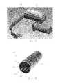
- the capacitor 40generally comprises a body or housing 46 , a first anode terminal 48 , a second cathode terminal 50 , dielectric material 52 , and a third output or ground terminal 54 .
- a first anode terminal 48is a positive/input terminal
- the second terminal 50is a negative terminal
- the third terminal 54is a positive/output terminal (or ground terminal).
- FIG. 6shows the capacitor without showing the housing and the dielectric material.
- the capacitor 40can be connected to the flex cable 44 with the first terminal 48 , second terminal 50 and the third terminal 54 being electrically, directly connected to conductors of the cable, such as by solder.
- the housing 46is comprised of electrically conductive metal, such as in the form of a can.
- the housing 46has an aperture 58 into the housing.
- a seal or closure 60is provide at the aperture 58 .
- the three terminals 48 , 50 , 54extend through the closure at a first end side of the capacitor.
- the capacitor 40also includes two plates 62 , 64 .
- the first plate 62is connected to the first terminal 48 to form a first electrical conductor for the capacitor.
- the second plate 64is connected to the second terminal 50 to form a second electrical conductor for the capacitor.
- the two plates 62 , 64are provided with a general coil shape or winding roll shape.
- the two plates 62 , 64are inter-rolled with each other with the dielectric material 52 therebetween. As seen by arrow 66 in FIG. 6 , capacitance can be provided between the first and second terminals 48 , 50 .
- First terminal 48is connected to a first end of the first plate 62 .
- the third terminal 54is connected to a second opposite end of the first plate 62 . Because of the coiled shape of the first plate 62 , this can provide an inductor with inductance between the first and third electrodes 48 , 54 as indicated by arrow 68 in FIG. 6 .
- the device 10can function as both a capacitor and a coil inductor.
- the inventioncan add one or more terminals to a capacitor so that the natural inductance of the capacitor, beneficially a roll, impacts between the input and output rather than between the capacitor itself and the terminal (where it would otherwise have a harmful impact in some cases). Furthermore, with the invention the output terminal 54 can be used for grounding the capacitor. This can add extra noise reduction and electric radiation immunity.
- FIG. 7A circuit diagram illustrating the new combined capacitor and inductor device 40 is shown in FIG. 7 . As can be seen, the inductor is one of the plates of the capacitor. Thus, the inductor is not arranged in series with the capacitor. The parallel capacitor-inductor arrangement is intertwined or intermixed, and are not spaced from each other.
- the inventioncan comprise a three to four legged capacitor (for example electrolytic or ceramic). Two of the contact points or terminals are placed proximate opposite ends of a first one of the capacitor plates, and the other capacitor plate can have either one or two terminals.
- the inventioncan comprise the concept of having an inductance component in a capacitor body; the construction of a such capacitor; the method of utilizing such a capacitor in both separating power networks (Radio Frequency, for example) and using it in controlling the timing of turn-off point and noise.
- the inductance of the capacitorwould reduce noise.
- the inventioncan comprise use of one or more of the capacitors 40 as an input or output to an apparatus 74 (or part of an apparatus) such as when the apparatus 74 is a SPMS for example. So, there are at least two applications benefiting of the roll inductance of a capacitor.
- the inventioncan be used for a power capacitor construction that is used, for example, in a Switch Mode Power Supply (SMPS) or a xenon flash for a camera.
- SMPSSwitch Mode Power Supply
- xenon flashfor a camera.
- a second ground or output terminalcan enable a separate ground pin configuration.
- the device 80comprises the first, second and third terminals 48 , 50 , 54 , and a fourth terminal 82 .
- the fourth terminal 82is a ground or output terminal connected to an end of the second plate 64 at the opposite end of the plate from the second terminal 50 .
- FIG. 11shows another embodiment where the fourth terminal 82 is connected to the housing 46 at the opposite end of the housing from the aperture 58 .
- an apparatuscomprising an electrical component and a flash.
- the electrical componentincludes a plurality of electrical conductors.
- the electrical componentcould be a printed circuit board or the flex cable 44 .
- the flashis connected to the conductors,
- the flashcomprises a flash lamp 38 and an electrical device 40 .
- the electrical device 40comprises a capacitor and an inductor with a common electrical conductor having a winding roll shaped section 62 which forms a winding plate of the capacitor and a coil of the inductor.
- the electrical componentcould be any suitable electrical component having electrical conductors.
- the apparatuscould be the subassembly shown in FIG. 3 , or the apparatus 10 shown in FIG. 1 , for example.
- the electrical devicecould be directly connected to the conductors of the flash lamp.
- an apparatusincluding a first electrical conductor ( 48 , 62 ), a second electrical conductor ( 50 , 64 ), dielectric material 52 connecting the first and second conductors to each other, and an output or ground terminal section 54 .
- the first electrical conductorhas a first terminal section 48 and a first plate section 62 .
- the second electrical conductorincludes a second terminal section 50 and a second plate section 64 .
- the second terminal sectionis connected to a first end of the second plate section.
- the second plate sectionincludes a coil shaped section.
- the output terminal sectionis connected to an opposite second end of the second plate section.
- the dielectric materialconnects the first and second plate sections to each other.
- an apparatuscomprising a capacitor and an output terminal 54 .
- the capacitorcomprises a first coil shaped plate 62 connected to a first terminal 48 , a second coil shaped plate 64 connected to a second terminal 50 , and dielectric material 52 connecting the first and second plates to each other in a spaced inter-rolled fashion.
- the output terminalis connected to the second plate at a location spaced from the second terminal.
- the second terminal, the second plate and the output terminalform an inductor such that the second coil shaped plate is a common member of both the capacitor and the inductor.
- an apparatuscomprising a capacitor comprising a first terminal 48 and a winding roll plate 62 connected to the first terminal; and an inductor comprising an input 48 , an output 54 and the winding roll plate 62 .
- the inputcomprises the first terminal of the capacitor
- the outputcomprises an output terminal extending from the winding roll plate proximate an opposite end of the plate relative to the first terminal.
- a methodcomprising providing an electrical device as indicated by block 84 ; and connecting an apparatus to the electrical device as indicated by block 86 .
- the apparatuscomprises a capacitor and an inductor having a common member forming a winding roll plate of the capacitor and a coil of the inductor.
- the common memberis configured to provide inductance to reduce noise of the electrical device.
- a methodcomprising turning ON current to an apparatus from a combined capacitor and inductor device as indicated by block 88 , wherein a capacitor and an inductor of the device comprise a common member forming a winding roll plate of the capacitor and a coil of the inductor; and turning OFF the current from the capacitor to the apparatus as indicated by block 90 , wherein a slope of the current from ON to OFF is increased as indicated by block 92 by inductance from the combined capacitor and inductor device to delay a current turn off point of the current from the capacitor.
- the inventioncan be used to provide a ground when the capacitor is manufactured. Thus, there is no need for the xenon flash supplier to perform an extra manufacturing process to provide a grounding connection for a capacitor.
- the capacitoris automatically grounded when the terminal 54 is connected to ground.
- the inventioncan be provided by a camera module manufacturer or a flash module manufacturer to a device manufacturer, such as a manufacturer of a mobile telephone handset for example.
- the inventioncould be used in suitable multifunction devices having a camera function with a flash.
- the inventioncan also be used in a stand alone digital camera rather than a multifunction device.
- the inventioncan also be used in a device other than for a camera function.
- the inventioncould be provided as a flash module configured to be inserted into a device as a single subassembly, such as shown in FIG. 3 for example.
- the device 100comprises positive capacitor plates 102 and negative capacitor plates 104 with ceramic material (not shown) therebetween.
- the ceramic materialfunctions as the dielectric material among the plates 102 / 104 .
- the plates 102 , 104are substantially flat and straight. Thus, the plates do not need to have a roll or coil shape.
- a negative terminal 106is connected to a first end of the negative plates 104 .
- a positive/input terminal 108is connected to a first end of the positive plates 102 , and a positive/output terminal 110 is connected to an opposite second end of the plates 102 .
- capacitancecan be provided between the negative terminal 106 and the positive terminals 108 , 110 .
- Inductancecan be provided between the positive/input terminal 108 and the positive/output terminal 110 as indicated by arrow 114 .
- the inventioncan be used in a capacitor other than a coiled plate electrolytic capacitor design, and other than a coiled conductor inductor design.
Landscapes
- Engineering & Computer Science (AREA)
- Power Engineering (AREA)
- Microelectronics & Electronic Packaging (AREA)
- Manufacturing & Machinery (AREA)
- Physics & Mathematics (AREA)
- General Physics & Mathematics (AREA)
- Stroboscope Apparatuses (AREA)
- Camera Bodies And Camera Details Or Accessories (AREA)
Abstract
Description
- Additional inductance and resistance between an input and an output can reduce noise in a Switch Mode Power Supply.
- Currently, a discrete resistor or inductance and a second capacitor are used for noise reduction in a Switch Mode Power Supply. These two components can be eliminated. This can provided a noticeable cost reduction.
- A Second ground or output terminal can enable a separate ground pin configuration.
- In a xenon flash grounding is needed. Currently the grounding is made by gluing the can (housing) to a ground. By eliminating this type of manufacturing step, there can be a remarkable cost reduction.
- Additional inductance benefits a xenon flash by improving the accuracy of short flash pulses.
- Additional inductance benefits a xenon flash by changing the color temperature to more beneficial area.
Claims (18)
Priority Applications (3)
| Application Number | Priority Date | Filing Date | Title |
|---|---|---|---|
| US12/215,261US8908350B2 (en) | 2008-06-25 | 2008-06-25 | Capacitor |
| PCT/FI2009/050340WO2009156560A1 (en) | 2008-06-25 | 2009-04-29 | Capacitor |
| US14/535,472US20150062860A1 (en) | 2008-06-25 | 2014-11-07 | Capacitor |
Applications Claiming Priority (1)
| Application Number | Priority Date | Filing Date | Title |
|---|---|---|---|
| US12/215,261US8908350B2 (en) | 2008-06-25 | 2008-06-25 | Capacitor |
Related Child Applications (1)
| Application Number | Title | Priority Date | Filing Date |
|---|---|---|---|
| US14/535,472ContinuationUS20150062860A1 (en) | 2008-06-25 | 2014-11-07 | Capacitor |
Publications (2)
| Publication Number | Publication Date |
|---|---|
| US20090323251A1 US20090323251A1 (en) | 2009-12-31 |
| US8908350B2true US8908350B2 (en) | 2014-12-09 |
Family
ID=41444070
Family Applications (2)
| Application Number | Title | Priority Date | Filing Date |
|---|---|---|---|
| US12/215,261Expired - Fee RelatedUS8908350B2 (en) | 2008-06-25 | 2008-06-25 | Capacitor |
| US14/535,472AbandonedUS20150062860A1 (en) | 2008-06-25 | 2014-11-07 | Capacitor |
Family Applications After (1)
| Application Number | Title | Priority Date | Filing Date |
|---|---|---|---|
| US14/535,472AbandonedUS20150062860A1 (en) | 2008-06-25 | 2014-11-07 | Capacitor |
Country Status (2)
| Country | Link |
|---|---|
| US (2) | US8908350B2 (en) |
| WO (1) | WO2009156560A1 (en) |
Families Citing this family (2)
| Publication number | Priority date | Publication date | Assignee | Title |
|---|---|---|---|---|
| JP6861567B2 (en)* | 2017-04-19 | 2021-04-21 | 矢崎総業株式会社 | Vehicle circuit |
| TWI866450B (en)* | 2023-09-08 | 2024-12-11 | 欣興電子股份有限公司 | Circuit board structure and manufacturing method thereof |
Citations (28)
| Publication number | Priority date | Publication date | Assignee | Title |
|---|---|---|---|---|
| US1460390A (en) | 1920-05-21 | 1923-07-03 | William J O'leary | Solenoid |
| US2521513A (en) | 1948-08-18 | 1950-09-05 | Gen Electric | Stationary induction apparatus |
| US2840694A (en)* | 1953-05-08 | 1958-06-24 | Rca Corp | Portable radio transmitter with combination microphone horn and antenna |
| US3025431A (en)* | 1958-06-27 | 1962-03-13 | Gen Electric | Flash apparatus |
| US3671885A (en)* | 1970-10-20 | 1972-06-20 | Lindsay Specialty Prod Ltd | High frequency signal routing devices for use in catv systems |
| US3691435A (en)* | 1970-11-23 | 1972-09-12 | Gen Electric | Wound impedence device |
| GB1315878A (en) | 1970-07-17 | 1973-05-02 | Phase Industries | Tubular electronic reactor component having an embedded electrode |
| US3775720A (en)* | 1970-11-23 | 1973-11-27 | Gen Electric | Cap-reactor power groove ballast circuit |
| US3782258A (en)* | 1971-12-03 | 1974-01-01 | Philips Corp | Ignition arrangement for a discharge tube |
| US3870392A (en)* | 1973-11-14 | 1975-03-11 | Whirlpool Co | Grounding mounting means |
| US4320364A (en) | 1979-06-11 | 1982-03-16 | Murata Manufacturing Co., Ltd. | Capacitor arrangement |
| US4368407A (en)* | 1979-08-31 | 1983-01-11 | Frequency Technology, Inc. | Inductor-capacitor impedance devices and method of making the same |
| US5040094A (en) | 1988-12-26 | 1991-08-13 | Murata Manufacturing Co., Ltd. | 3-terminal capacitor |
| US5103147A (en)* | 1988-07-14 | 1992-04-07 | Bsg-Schalttechnik Gmbh & Co. Kg | Operating device for consumers connected to the electric system of mobile units |
| US5153812A (en) | 1989-06-16 | 1992-10-06 | Mitsubishi Denki Kabushiki Kaisha | Composite LC element |
| US5337028A (en) | 1992-05-27 | 1994-08-09 | Sundstrand Corporation | Multilayered distributed filter |
| US5367275A (en)* | 1991-01-23 | 1994-11-22 | Mitsubishi Denki Kabushiki Kaisha | Laminate LC filter having combined condenser and coil functions |
| US5515126A (en)* | 1994-09-28 | 1996-05-07 | Eastman Kodak Company | Convertible flash camera and method |
| US5522851A (en)* | 1994-12-06 | 1996-06-04 | Ventritex, Inc. | Capacitor for an implantable cardiac defibrillator |
| US5892668A (en)* | 1996-06-10 | 1999-04-06 | Fuji Electric Company, Ltd. | Noise-cut filter for power converter |
| US5920292A (en)* | 1996-12-20 | 1999-07-06 | Ericsson Inc. | L-band quadrifilar helix antenna |
| US6204817B1 (en)* | 1998-09-28 | 2001-03-20 | Allgon Ab | Radio communication device and an antenna system |
| US6255935B1 (en)* | 1998-09-14 | 2001-07-03 | Abb Research Ltd. | Coupling capacitor having an integrated connecting cable |
| US6529363B2 (en)* | 2000-06-21 | 2003-03-04 | Koninklijke Philips Electronics N.V. | Capacitor integrated into transformer by multi-layer foil winding |
| US6661644B2 (en)* | 2001-10-05 | 2003-12-09 | Matsushita Electric Industrial Co., Ltd. | Capacitor |
| US6836401B2 (en)* | 2001-09-20 | 2004-12-28 | Matsushita Electric Industrial Co., Ltd. | Capacitor, laminated capacitor, and capacitor built-in-board |
| US20070086146A1 (en)* | 2005-10-18 | 2007-04-19 | Mark Timmerman | Capacitor bank for electrical generator |
| US7385804B2 (en)* | 2003-08-12 | 2008-06-10 | Rohm Co., Ltd. | Solid electrolytic capacitor, electric circuit, and solid electrolytic capacitor mounting structure |
Family Cites Families (2)
| Publication number | Priority date | Publication date | Assignee | Title |
|---|---|---|---|---|
| US4132471A (en)* | 1977-04-04 | 1979-01-02 | Polaroid Corporation | Expandable self-developing camera |
| JP4288134B2 (en)* | 2003-10-16 | 2009-07-01 | 京セラ株式会社 | Imaging device |
- 2008
- 2008-06-25USUS12/215,261patent/US8908350B2/ennot_activeExpired - Fee Related
- 2009
- 2009-04-29WOPCT/FI2009/050340patent/WO2009156560A1/enactiveApplication Filing
- 2014
- 2014-11-07USUS14/535,472patent/US20150062860A1/ennot_activeAbandoned
Patent Citations (28)
| Publication number | Priority date | Publication date | Assignee | Title |
|---|---|---|---|---|
| US1460390A (en) | 1920-05-21 | 1923-07-03 | William J O'leary | Solenoid |
| US2521513A (en) | 1948-08-18 | 1950-09-05 | Gen Electric | Stationary induction apparatus |
| US2840694A (en)* | 1953-05-08 | 1958-06-24 | Rca Corp | Portable radio transmitter with combination microphone horn and antenna |
| US3025431A (en)* | 1958-06-27 | 1962-03-13 | Gen Electric | Flash apparatus |
| GB1315878A (en) | 1970-07-17 | 1973-05-02 | Phase Industries | Tubular electronic reactor component having an embedded electrode |
| US3671885A (en)* | 1970-10-20 | 1972-06-20 | Lindsay Specialty Prod Ltd | High frequency signal routing devices for use in catv systems |
| US3691435A (en)* | 1970-11-23 | 1972-09-12 | Gen Electric | Wound impedence device |
| US3775720A (en)* | 1970-11-23 | 1973-11-27 | Gen Electric | Cap-reactor power groove ballast circuit |
| US3782258A (en)* | 1971-12-03 | 1974-01-01 | Philips Corp | Ignition arrangement for a discharge tube |
| US3870392A (en)* | 1973-11-14 | 1975-03-11 | Whirlpool Co | Grounding mounting means |
| US4320364A (en) | 1979-06-11 | 1982-03-16 | Murata Manufacturing Co., Ltd. | Capacitor arrangement |
| US4368407A (en)* | 1979-08-31 | 1983-01-11 | Frequency Technology, Inc. | Inductor-capacitor impedance devices and method of making the same |
| US5103147A (en)* | 1988-07-14 | 1992-04-07 | Bsg-Schalttechnik Gmbh & Co. Kg | Operating device for consumers connected to the electric system of mobile units |
| US5040094A (en) | 1988-12-26 | 1991-08-13 | Murata Manufacturing Co., Ltd. | 3-terminal capacitor |
| US5153812A (en) | 1989-06-16 | 1992-10-06 | Mitsubishi Denki Kabushiki Kaisha | Composite LC element |
| US5367275A (en)* | 1991-01-23 | 1994-11-22 | Mitsubishi Denki Kabushiki Kaisha | Laminate LC filter having combined condenser and coil functions |
| US5337028A (en) | 1992-05-27 | 1994-08-09 | Sundstrand Corporation | Multilayered distributed filter |
| US5515126A (en)* | 1994-09-28 | 1996-05-07 | Eastman Kodak Company | Convertible flash camera and method |
| US5522851A (en)* | 1994-12-06 | 1996-06-04 | Ventritex, Inc. | Capacitor for an implantable cardiac defibrillator |
| US5892668A (en)* | 1996-06-10 | 1999-04-06 | Fuji Electric Company, Ltd. | Noise-cut filter for power converter |
| US5920292A (en)* | 1996-12-20 | 1999-07-06 | Ericsson Inc. | L-band quadrifilar helix antenna |
| US6255935B1 (en)* | 1998-09-14 | 2001-07-03 | Abb Research Ltd. | Coupling capacitor having an integrated connecting cable |
| US6204817B1 (en)* | 1998-09-28 | 2001-03-20 | Allgon Ab | Radio communication device and an antenna system |
| US6529363B2 (en)* | 2000-06-21 | 2003-03-04 | Koninklijke Philips Electronics N.V. | Capacitor integrated into transformer by multi-layer foil winding |
| US6836401B2 (en)* | 2001-09-20 | 2004-12-28 | Matsushita Electric Industrial Co., Ltd. | Capacitor, laminated capacitor, and capacitor built-in-board |
| US6661644B2 (en)* | 2001-10-05 | 2003-12-09 | Matsushita Electric Industrial Co., Ltd. | Capacitor |
| US7385804B2 (en)* | 2003-08-12 | 2008-06-10 | Rohm Co., Ltd. | Solid electrolytic capacitor, electric circuit, and solid electrolytic capacitor mounting structure |
| US20070086146A1 (en)* | 2005-10-18 | 2007-04-19 | Mark Timmerman | Capacitor bank for electrical generator |
Non-Patent Citations (1)
| Title |
|---|
| Perkinelmer Optoelectronics, High Performance Flash and Arc Lamps. Brochure (online). Created on Oct. 9, 2009, modified Sep. 25, 2006. |
Also Published As
| Publication number | Publication date |
|---|---|
| WO2009156560A1 (en) | 2009-12-30 |
| US20090323251A1 (en) | 2009-12-31 |
| US20150062860A1 (en) | 2015-03-05 |
Similar Documents
| Publication | Publication Date | Title |
|---|---|---|
| EP2106014B1 (en) | Dc-dc converter module | |
| US9390862B2 (en) | Composite electronic component and board with the same mounted thereon | |
| CN104600974B (en) | Combined electronical assembly and the plate installed above for having the combined electronical assembly | |
| US20140313785A1 (en) | Composite electronic component, board having the same mounted thereon and power stabilizing unit including the same | |
| US9633779B2 (en) | Composite electronic component and board having the same | |
| KR101504017B1 (en) | Multi-layered ceramic capacitor and board for mounting the same | |
| US20150062860A1 (en) | Capacitor | |
| US9532443B2 (en) | Composite electronic component and board having the same | |
| CN104111714B (en) | Composite electronic assemblies, boards and power smoothing units | |
| US9922762B2 (en) | Composite electronic component and board having the same | |
| KR101659135B1 (en) | Composite electronic component, board having the same mounted thereon and power smoothing unit comprising the same | |
| KR101539857B1 (en) | Composite electronic component and board for mounting the same | |
| JP4184336B2 (en) | Flexible flat conductor with built-in output filter | |
| US9754723B2 (en) | Composite electronic component and board for mounting thereof | |
| KR102004778B1 (en) | Composite electronic component, board having the same mounted thereon and power smoothing unit comprising the same | |
| KR101983153B1 (en) | Composite electronic component | |
| KR101558075B1 (en) | Composite electronic component and board for mounting the same | |
| KR101452138B1 (en) | Composite electronic component | |
| US20160181011A1 (en) | Composite electronic component |
Legal Events
| Date | Code | Title | Description |
|---|---|---|---|
| AS | Assignment | Owner name:NOKIA CORPORATION, FINLAND Free format text:ASSIGNMENT OF ASSIGNORS INTEREST;ASSIGNOR:NASKALI, MATTI;REEL/FRAME:021657/0813 Effective date:20080715 Owner name:NOKIA CORPORATION, FINLAND Free format text:ASSIGNMENT OF ASSIGNORS INTEREST;ASSIGNOR:WALLIUS, SAMULI;REEL/FRAME:021657/0817 Effective date:20080804 Owner name:NOKIA CORPORATION, FINLAND Free format text:ASSIGNMENT OF ASSIGNORS INTEREST;ASSIGNOR:YLA-SOININMAKI, LASSI;REEL/FRAME:021657/0837 Effective date:20080715 | |
| AS | Assignment | Owner name:MICROSOFT CORPORATION, WASHINGTON Free format text:SHORT FORM PATENT SECURITY AGREEMENT;ASSIGNOR:CORE WIRELESS LICENSING S.A.R.L.;REEL/FRAME:026894/0665 Effective date:20110901 Owner name:NOKIA CORPORATION, FINLAND Free format text:SHORT FORM PATENT SECURITY AGREEMENT;ASSIGNOR:CORE WIRELESS LICENSING S.A.R.L.;REEL/FRAME:026894/0665 Effective date:20110901 | |
| AS | Assignment | Owner name:NOKIA 2011 PATENT TRUST, DELAWARE Free format text:ASSIGNMENT OF ASSIGNORS INTEREST;ASSIGNOR:NOKIA CORPORATION;REEL/FRAME:027120/0608 Effective date:20110531 Owner name:2011 INTELLECTUAL PROPERTY ASSET TRUST, DELAWARE Free format text:CHANGE OF NAME;ASSIGNOR:NOKIA 2011 PATENT TRUST;REEL/FRAME:027121/0353 Effective date:20110901 | |
| AS | Assignment | Owner name:CORE WIRELESS LICENSING S.A.R.L, LUXEMBOURG Free format text:ASSIGNMENT OF ASSIGNORS INTEREST;ASSIGNOR:2011 INTELLECTUAL PROPERTY ASSET TRUST;REEL/FRAME:027485/0472 Effective date:20110831 | |
| STCF | Information on status: patent grant | Free format text:PATENTED CASE | |
| CC | Certificate of correction | ||
| AS | Assignment | Owner name:MICROSOFT CORPORATION, WASHINGTON Free format text:UCC FINANCING STATEMENT AMENDMENT - DELETION OF SECURED PARTY;ASSIGNOR:NOKIA CORPORATION;REEL/FRAME:039872/0112 Effective date:20150327 | |
| AS | Assignment | Owner name:CONVERSANT WIRELESS LICENSING S.A R.L., LUXEMBOURG Free format text:CHANGE OF NAME;ASSIGNOR:CORE WIRELESS LICENSING S.A.R.L.;REEL/FRAME:044250/0398 Effective date:20170720 | |
| MAFP | Maintenance fee payment | Free format text:PAYMENT OF MAINTENANCE FEE, 4TH YEAR, LARGE ENTITY (ORIGINAL EVENT CODE: M1551) Year of fee payment:4 | |
| AS | Assignment | Owner name:CPPIB CREDIT INVESTMENTS, INC., CANADA Free format text:AMENDED AND RESTATED U.S. PATENT SECURITY AGREEMENT (FOR NON-U.S. GRANTORS);ASSIGNOR:CONVERSANT WIRELESS LICENSING S.A R.L.;REEL/FRAME:046897/0001 Effective date:20180731 | |
| AS | Assignment | Owner name:CONVERSANT WIRELESS LICENSING S.A R.L., LUXEMBOURG Free format text:RELEASE BY SECURED PARTY;ASSIGNOR:CPPIB CREDIT INVESTMENTS INC.;REEL/FRAME:055910/0698 Effective date:20210302 | |
| FEPP | Fee payment procedure | Free format text:MAINTENANCE FEE REMINDER MAILED (ORIGINAL EVENT CODE: REM.); ENTITY STATUS OF PATENT OWNER: LARGE ENTITY | |
| LAPS | Lapse for failure to pay maintenance fees | Free format text:PATENT EXPIRED FOR FAILURE TO PAY MAINTENANCE FEES (ORIGINAL EVENT CODE: EXP.); ENTITY STATUS OF PATENT OWNER: LARGE ENTITY | |
| STCH | Information on status: patent discontinuation | Free format text:PATENT EXPIRED DUE TO NONPAYMENT OF MAINTENANCE FEES UNDER 37 CFR 1.362 | |
| FP | Lapsed due to failure to pay maintenance fee | Effective date:20221209 |