US8904148B2 - Processor architecture with switch matrices for transferring data along buses - Google Patents
Processor architecture with switch matrices for transferring data along busesDownload PDFInfo
- Publication number
- US8904148B2 US8904148B2US13/176,381US201113176381AUS8904148B2US 8904148 B2US8904148 B2US 8904148B2US 201113176381 AUS201113176381 AUS 201113176381AUS 8904148 B2US8904148 B2US 8904148B2
- Authority
- US
- United States
- Prior art keywords
- array
- data
- bus
- processor architecture
- elements
- Prior art date
- Legal status (The legal status is an assumption and is not a legal conclusion. Google has not performed a legal analysis and makes no representation as to the accuracy of the status listed.)
- Expired - Fee Related
Links
Images


Classifications
- G—PHYSICS
- G06—COMPUTING OR CALCULATING; COUNTING
- G06F—ELECTRIC DIGITAL DATA PROCESSING
- G06F15/00—Digital computers in general; Data processing equipment in general
- G06F15/76—Architectures of general purpose stored program computers
- G06F15/80—Architectures of general purpose stored program computers comprising an array of processing units with common control, e.g. single instruction multiple data processors
- G06F15/8007—Architectures of general purpose stored program computers comprising an array of processing units with common control, e.g. single instruction multiple data processors single instruction multiple data [SIMD] multiprocessors
- G06F15/8023—Two dimensional arrays, e.g. mesh, torus
Definitions
- This inventionrelates to a processor architecture, and in particular to an architecture which can be used in a wide range of devices, such as communications devices operating under different standards.
- the processor architecture of the present inventionfalls under the broad category of what are sometimes referred to as dataflow architectures, but with some key differences which address the needs of software.
- the inventionprovides a solution which is more akin to a hard-wired architecture than a DSP processor, with consequential size and power advantages. It consists of an array of processor and memory elements connected by switch matrices.
- a processor architecturecomprising:
- each first bus pairincluding a respective first bus running in a first direction (for example, left to right) and a respective second bus running in a second direction is opposite to the first direction (for example right to left);
- each second bus pairincluding a respective third bus running in a third direction (for example downwards) and a respective fourth bus running in a fourth direction opposite to the third direction (for example upwards), the third and fourth buses intersecting the first and second buses;
- each switch matrixlocated at an intersection of a first and a second pair of buses;
- each elementbeing arranged to receive data from a respective first or second bus, and transfer data to a respective first or second bus.
- the elements in the arrayinclude processing elements, for operating on received data, and memory elements, for storing received data.
- the processing elementsinclude Arithmetic Logic Units and/or Multiplier Accumulators.
- the elements in the arrayfurther include interface elements for receiving input data from outside the processor, and transferring output data outside the processor.
- each element of the arrayis connected between a first bus of one first bus pair and a second bus of an adjacent first bus pair, and has: a first input for receiving data from the first bus of the one first bus pair; a first output for transferring data to the first bus of the one first bus pair; a second input for receiving data from a second bus of the adjacent first bus pair; and a second output for transferring data to the second bus of the adjacent first bus pair.
- each switch matrixallows data on a bus of a first bus pair to be switched onto the other bus of said first bus pair and/or onto either bus or both buses of the respective intersecting second bus pair, and allows data on a bus of a second bus pair to be switched onto either bus or both buses of the respective intersecting first bus pair, but not onto the other bus of said second bus pair.
- each bus of a first bus pair between each pair of adjacent switch matricesthere are a plurality of array elements (most preferably, four) connected to each bus of a first bus pair between each pair of adjacent switch matrices.
- the architecture according to the preferred embodiment of the inventionhas the advantage that no global memory is required, which provides a major benefit in terms of power consumption.
- the architectureallows flexible data routing between array elements using a switch matrix. This means that the device is able to run the many diverse algorithms required by a software radio concurrently, without having to reconfigure the array.
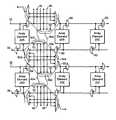
- FIG. 1is a schematic representation of a section of a processor, illustrating the architecture in accordance with the invention
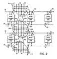
- FIG. 2is an enlarged representation of a part of the architecture of FIG. 1 ;
- FIG. 3is an enlarged representation of another part of the architecture of FIG. 1 ;
- FIG. 4is an enlarged representation of another part of the architecture of FIG. 1 ;
- FIG. 5shows the distribution of elements in a typical array in accordance with the invention
- FIG. 6shows a first array element in the architecture of FIG. 1 ;
- FIG. 7shows a second array element in the architecture of FIG. 1 ;
- FIG. 8shows a first connection of the array element of FIG. 7 in the array according to the invention
- FIG. 9shows a second connection of the array element of FIG. 7 in the array according to the invention.
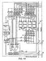
- FIG. 10shows a third array element in the architecture of FIG. 1 ;
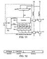
- FIG. 11shows a fourth array element in the architecture of FIG. 1 ;
- FIG. 12shows the format of data transferred between array elements
- FIG. 13is a timing diagram illustrating the flow of data between array elements.
- FIG. 1shows a part of the structure of a processor architecture 10 .
- the deviceis made up of an array of elements 20 , which are connected by buses and switches.
- the architectureincludes first bus pairs 30 , shown running horizontally in FIG. 1 , each pair including a respective first bus 32 carrying data from left to right in FIG. 1 and a respective second bus 36 carrying data from right to left.
- the architecturealso includes second bus pairs 40 , shown running vertically in FIG. 1 , each pair including a respective third bus 42 shown carrying data upwards in FIG. 1 and a respective fourth bus 46 shown carrying data downwards in FIG. 1 .
- each diamond connection 50represents a switch, which connects an array element 20 to a respective bus 32 , 36 .
- the arrayfurther includes a switch matrix 55 at each intersection of a first and second bus pair 30 , 40 .
- Each array elementcan be designed to be any one of the following:
- an execution array elementwhich contains an Arithmetic Logic Unit (ALU) or Multiplier Accumulator (MAC);
- ALUArithmetic Logic Unit
- MACMultiplier Accumulator
- a memory array elementcontaining a RAM
- an interface array elementwhich connects the processor to an external device
- a switch control array elementwhich controls the operation of at least one switch matrix 55 .
- FIG. 2is an enlarged view of a part of the architecture of FIG. 1 , showing six array elements, 20 A- 20 F. Each array element is connected onto two 64-bit buses, 32 , 36 , which carry data in opposite directions. After every four array elements (as shown in FIG. 1 ), the horizontal buses are connected to two vertical buses, 42 , 46 , one running up and the other down.
- the choice of bit-width and vertical bus pitchis not fundamental to the architecture, but these dimensions are presently preferred.
- Each switch element 50is a 2:1 multiplexer, controllable such that either of its two inputs can be made to appear on its output.
- output data from an array elementcan be transferred onto a bus, and/or data already on the bus can be allowed to pass.
- the switch matrix 55includes four 4:1 multiplexers 501 , 502 , 503 and 504 which are each controllable such that any one of their inputs can appear at their output.
- the inputs of multiplexer 501are connected to input connections 32 a , 36 a and 42 a on buses 32 , 36 , 42 respectively, and to ground.
- the output of multiplexer 501is connected to bus 42 .
- the inputs of multiplexer 502are connected to input connections 32 a , 36 a and 46 a on buses 32 , 36 , 46 respectively, and to ground.
- the output of multiplexer 502is connected to bus 46 .
- the inputs of multiplexer 503are connected to input connections 32 a , 36 a , 42 a and 46 a on buses 32 , 36 , 42 and 46 respectively.
- the output of multiplexer 503is connected to bus 36 .
- the inputs of multiplexer 504are connected to input connections 32 a , 36 a , 42 a and 46 a on buses 32 , 36 , 42 and 46 respectively.
- the output of multiplexer 504is connected to bus 32 .
- the input of any buscan be used as the source for data on the output of any bus, except that it is not possible to select the down bus (i.e. the one entering from the top of the diagram in FIG. 2 , namely the fourth bus 46 ) as the source for the up bus (that is, the third bus 42 ), and, similarly, it is not possible to select the up bus (the third bus 42 ) as the source of the down bus (the fourth bus 46 ).
- each of the multiplexers 501 , 502is connected to ground. That is, each of the 64 bus lines is connected to the value 0. This is used as part of a power reduction method, which will be described further below.
- Each of the multiplexers 501 , 502 , 503 , 504can be controlled by signals on two control lines. That is, a two-bit control signal can determine which of the four inputs to a multiplexer appears on its output.
- FIG. 3is a view of the top-left hand corner of the array of FIG. 1 , showing the structure of a switch matrix 56 which is used when there is no input connection to a left-right bus 32 , and of a switch matrix 57 which is used when there is no input connection to a left-right bus 32 or to a bus 46 running down.
- the switch matrix 56includes three 4:1 multiplexers 505 , 506 , 507 , while the switch matrix 57 includes three 4:1 multiplexers 508 , 509 , 510 .
- the number of input buses to multiplexers 505 , 508 and 509is reduced by one, because there is no input bus entering from the left.
- there is no input bus entering from the left as an input to multiplexer 510but in this case the input bus which has been released has been connected to 0.
- This is also the case for multiplexer 507but in this case there is no input bus entering from the top of the switch matrix either, so this multiplexer has only three input buses.
- FIG. 4is a view of part of the top edge of the array of FIG. 1 , showing the structure of a switch matrix 58 which is used when there is no input connection to a bus 46 running down.
- the switch matrix 58includes two 4:1 multiplexers 511 , 512 .
- the number of available input buses to multiplexers 511 and 512is reduced by two, but, in the case of multiplexer 511 , one of the input buses has been replaced by the value zero.
- An equivalent structure for multiplexers on the bottom edge of the arrayis apparent.
- Data transfercan be regarded as having three stages. Firstly, an array element puts the data on the appropriate output.
- multiplexers in the appropriate switch matrix, or switch matricesare switched to make the necessary connections.
- the destination array elementloads the data.
- Each of these aspectsis controlled by a separate array element: the first and third by the source and destination array elements respectively, and the second by special switch control array elements. These are embedded into the array at regular intervals and are connected by control lines to all the multiplexers in the switch matrices which they control. Each array element controls the multiplexers immediately adjacent to its outputs, with the control being performed separately on individual 16-bit fields. This allows several array elements to source data onto a bus at the same time, provided they are using different fields of the bus. This is particularly useful for functions such as Add-Compare-Select (ACS) in the Viterbi Algorithm. Switching at intersection nodes of the horizontal and vertical buses is performed on the entire 64-bit bus and its associated control signals.
- ACSAdd-Compare-Select
- each array elementmust run a program loop which accesses the buses in a regular pattern which has a duration in clock cycles which is a power of two (e.g. 4, 8, 16 or 32 clock cycles).
- array elementsare data driven. That is to say, array elements only execute instructions of their programs when data arrives.
- FIG. 5shows an example of an array containing 256 array elements in proportions optimised for a communications transceiver.
- FIG. 5does not show the horizontal buses in the array and the positions of pairs of vertical buses 40 are shown as single lines.
- the example array of FIG. 5contains three interface array elements, 80 , 81 and 82 .
- Array elements 80 and 81are used for data input and output to the analogue portions of the transceiver and array element 82 is the interface to a microprocessor.
- Each of the four Switch Control array elements 83 a to 83 dcontrols the switch matrices of one quarter of the array.
- Switch Control array element 83 acontrols the switch matrices along the horizontal buses connected to the top four rows of array elements, 84 .
- FIG. 6shows the preferred embodiment of a Switch Control array element. This consists of controller 94 and RAM 95 , together with means of loading the RAM using the Array Control Protocol described below and sequencing data out of the RAM. Data is loaded into the RAM from either the left bus 32 or right bus 36 to which the Switch Control array element is connected by means of multiplexers 92 and 64-bit register 93 .
- the address of RAM 95is first set to zero and the first 160-bit word is read out and loaded into register 96 .
- the RAM addressis incremented and a new 160-bit word is loaded into register 96 , until the address reaches 127, at which point it is reset to zero again and the process is repeated.
- the outputs of register 96are routed directly to the select inputs of the multiplexers in the switch matrices 55 ( FIGS. 1 and 2 ), so in this way all the switch matrices are controlled in a cyclical pattern lasting for 128 clock cycles.
- the outputs of register 96can also be directed onto the bus 32 or the bus 36 by means of a multiplexer 97 and switch boxes 51 .
- a multiplexer 97 and switch boxes 51As previously noted, most areas of the array transfer data in cyclical patterns of a duration less than 128 clock cycles, but these are accommodated by repeating them within the 128 cycle pattern.
- ALU and MAC array elementshave the same interfaces to the array, differing only in the type of execution unit and associated instructions.
- FIG. 7shows an ALU array element, which will be used to describe these interfaces to the array.
- three 64-bit registerseach formed from four 16-bit sub-registers 121 a - 121 d , 121 e - 121 h and 121 i - 121 l , can be connected to either of left bus 32 or right bus 36 through multiplexers 120 , thus allowing them to be loaded from either bus.
- any one 64-bit registercan be connected to the left or right bus during one clock cycle and any combination of sub-registers loaded.
- an instructionmay cause 16-bit sub-registers 121 a and 121 b of 64-bit register 121 a - 121 d to be loaded with the data in bits 31 : 0 of left bus 32 .
- Further instructionsmay cause data in the registers to be manipulated in ALU 125 and stored back into the same or different registers 121 , and still further instructions may enable the contents of these registers onto the left and right buses via multiplexer 126 and switch boxes 51 .
- one 64-bit registermay be used to load data from an array bus, data from another may be enabled back onto an array bus and ALU operations may be performed on the contents of registers, these tasks being accomplished by using separate fields in the instruction words.
- FIG. 8shows the contents of a switch box 51 in FIG. 7 .
- BUSIN 132 and BUSOUT 133are each segments of a left bus 36 or a right bus 32 .
- Control signals EN[ 3 : 0 ] 130 and SEL[ 3 : 0 ] 131are both sourced by instruction decode block 123 in FIG. 7 . Using these signals, any 16-bit field of BUSOUT may be set to be equal to BUSIN, the output bus of the array element or zero.
- FIG. 9illustrates how, likewise, the BDVAL signal (described below) associated with the data on the bus can be allowed to pass along the bus or be set by the array element.
- FIG. 10shows the preferred embodiment of a Memory array element. This has many of the same features of the ALU array element described above, but in addition has RAMs 143 connected to registers 140 , 141 and 142 via multiplexers. 16-bit sub-registers R 0 to R 3 of 64-bit register 140 are used for data input to the RAMs, 16-bit sub-registers R 4 to R 7 of 64-bit register 141 are used for the address input to the RAMs and 16-bit sub-registers R 8 to R 11 of 64-bit register 142 are used for the data output from the RAMs.
- Both address and datamay be manipulated using the ALU under the control of the instruction decode unit as in the case of the ALU array element and the processes of loading data from the left and right buses 32 and 36 is also performed in exactly the same manner.
- the instructions stored in instruction store 144 and decoded in instruction decode unit 145have an additional field compared to the equivalent units of the ALU array element. This additional field is used to control the reading of data from the RAMs and writing of data to them, these operations being performed in the same cycles as array accesses and ALU operations.
- addresses for the RAMsmay be calculated within the Memory array element using its internal ALU and loaded into the sub-registers of 64-bit register 141 .
- addressesmay be provided over the array buses from another array element and loaded directly into register 141 .
- Memory array elementshold all the data which is processed by the execution array elements and there is no external global memory.
- Interface array elementsaccess to external memory can be provided using appropriate Interface array elements.
- instructions which form the programs which the array elements runare not generally stored in Memory array elements, but reside entirely in the instruction stores of the array elements. Instructions are loaded into the instruction stores of the array elements using the Array Control Protocol, which is described below.
- FIG. 11shows how an Analogue to Digital Converter (ADC) 153 can be connected to the processor architecture as an Interface array element.
- ADCAnalogue to Digital Converter
- an ADCsolely sources data
- the only need to supply data to this array element, through a multiplexer 150is for the purposes of configuration and control, such as putting the ADC into test or low power standby modes, and to control the times at which the array element transfers sampled data onto the output bus.
- the array element controller 152can therefore be simpler than the instruction store and decode unit in Execution and Memory array elements, but nevertheless is capable of being programmed to cause ADC 153 to sample input analogue signal 156 , load the sampled data into register 155 through multiplexers 154 and enable this data onto bus 32 or 36 at configurable points in a sequence.
- Interface array elementOther common sorts of Interface array element are the Digital to Analogue Converters (DAC) array element, which performs the opposite role of the ADC array element, and the host interface array element. The latter transfers data from the array to the bus of a general purpose host processor and from the host processor to the array.
- DACDigital to Analogue Converters
- a number of control signalsare multiplexed with the 64-bit data buses in the array, namely:
- ARRCTLARRay ConTroL—This signifies that the data on the bus is array control information. All array elements must interpret this and act accordingly.
- BDVALBus Data VALid—This signifies that there is valid data on the bus. This is a key signal in the control of power dissipation.
- ACPArray Control Protocol
- Each array elementhas a Unique Identifier (UID), which is used to address it, and the ACP uses Array Control Words (ACW's) to communicate information between array elements.
- UIDUnique Identifier
- ACW'sArray Control Words
- FIG. 12shows the structure of the 64-bit ACW.
- the array elementWhen an ACW is put on the section of the bus to which an array element is connected, the array element must examine the word, even if it was formerly in low-power sleep mode. If the address field of the ACW matches the UID of the array element, or is equal to a designated broadcast address, the array element must interpret the FUNCTION field of the ACW and perform the required action. In one presently preferred embodiment of the invention, the following FUNCTION fields are defined:
- the DATA fieldcontains a program word which Program must be placed in the first location in the 0 program store of the array element 11 Load
- the DATA fieldcontains a program word which Program must be placed in the next location in the program store of the array element 100 Start The array element must start executing program in program store 101 Stop The array element must stop executing program in program store 110 Test Enter test mode 111 Dump Place data from next location in the program store on the bus
- ACWsmay be generated by any array element, but the array will normally include one element which is defined as the master controller, and the master controller will generate all ACWs.
- the major function of the Array Control Protocolis to load the program stores of the array elements when the device is booted. Therefore, a host interface array element, which loads the program supplied by a host processor, is most likely to be the source of ACWs.
- the processor of the present inventionUnlike most processors, which are instruction driven, the processor of the present invention, and its component array elements, are data driven. That is, instead of processing data as the result of fetching an instruction, array elements execute instructions as a result of receiving data.
- the demodulatorwill contain an ADC which samples at a fixed rate which generally will be somewhat above the actual required rate.
- the front end of the demodulatorwill contain an interpolator, which resamples the incoming data. This removes the need for an analogue VCO to synchronise the ADC sample clock to the data, but the resampled data will be irregular with respect to the processor system clock and data transfer sequences, creating “gaps” where data would have been expected. (In fact the ADC sample clock need not be synchronised to the processor system clock at all, with synchronisation to the system clock being performed in the ADC interface array element).
- the array elementswhich are affected merely “go to sleep” until data is available.
- array elementswill sleep for at least one of the sequences to which they are synchronised.
- FIG. 13This is illustrated in FIG. 13 .
- all transfers to two array elementsare synchronised to a four cycle sequence.
- Successive transfer sequencesare labelled 0 to 5 (TRANSFER SEQ).
- array element Aloads data on the fourth clock cycle and array element B on the second (as shown in the DATA bus), the points at which they load being shown for convenience as the signals LOADREQA and LOADREQB.
- Signals BDVALA and BDVALBare the BDVAL signals associated with the data loaded by array elements A and B.
- a small group of array elementswhen a particular array element does not receive data, a small group of array elements must be stalled. For example, if an array element multiplies data with coefficients which are loaded from a memory array element, then, if the data does not arrive, the memory array element must be prevented from sending data. This is achieved by routing the data past the memory array element and allowing the memory array element to sample the BDVAL signal. If BDVAL is low, then the memory array element will also go into sleep mode.
- the method by which the BDVAL signal is controlled and array elements respond to itis as follows.
- this array elementexecutes a STORE instruction, which causes it to enable data onto an array bus, it sets the LOCAL_VALID, VALID_ENABLE and SELECT signals ( 128 a in FIG. 9 ) for one of switch boxes 52 such that BDVAL OUT ( 129 in FIG. 9 ) is set to 1 for one clock cycle.
- EN[ 3 : 0 ] 130 and SEL[ 3 : 0 ] 131 in FIG. 8are set so as to set BUSOUT[ 63 : 0 ] to the required value.
- array element 20 Bcould transfer data onto bits [ 31 : 0 ] of bus 36
- array element 20 Ctransfers data on bits [ 63 : 32 ], with all 64 bits being routed to array element 20 F, say.
- the Switch Control array elementscause multiplexers in switch matrices 55 ( FIGS. 1 and 2 ) to switch so that the bus data and the associated BDVAL signal are routed to the destination array element.
- the destination array elementexecutes a LOAD instruction which causes multiplexers 120 to select the bus on the inputs of the required register 121 , which is loaded at the end of the clock cycle if the BDVAL signal is 1. If the BDVAL signal is 0, no load takes place and the array element waits for a number of clock cycles specified as part of the LOAD instruction field.
- the only active circuitry in the array elementis the execution control block 124 , which loads the wait period into a counter and counts down. When the count reaches zero, the execution control unit re-examines the BDVAL signal and, if it is now 1, causes execution to proceed from the point it left off. Because the circuitry in the execution control unit is very small compared to the rest of the array element, very little power is consumed while an array element is waiting.
- all array elements which can be destinations for data transfersalso have a WAIT instruction.
- This instructioncauses the execution control unit to examine the BDVAL signal for either left bus 32 or right bus 36 and wait for the specified number of clock cycles if selected BDVAL signal is 0. However, no data is loaded.
- bus lines and other signalsare not charged and discharged unless necessary.
- the default state of all bus lineshas been chosen to be 0, and the Switch Control array elements are programmed to select the value of 0 onto all bus segments that are not being used via the “0” inputs of multiplexers 501 and 502 in FIG. 2 and additional multiplexer inputs at the edges and corners of the array as shown in FIGS. 3 and 4 .
- a fieldis provided in the LOAD instruction which is executed on an array element which selects whether data is allowed to propagate further along the bus or is stopped as just described, thus allowing multiple array elements to load the same-data (or different fields of the bus which are transferred during the same clock cycle).
- processor architecturewhich can be reprogrammed to provide a required functionality, while being efficient in terms of its power consumption and occupied silicon area.
Landscapes
- Engineering & Computer Science (AREA)
- Computer Hardware Design (AREA)
- Theoretical Computer Science (AREA)
- Computing Systems (AREA)
- Physics & Mathematics (AREA)
- General Engineering & Computer Science (AREA)
- General Physics & Mathematics (AREA)
- Multi Processors (AREA)
- Bus Control (AREA)
Abstract
Description
| Function | Description | ||
| 0 | Reset | Causes the array element to halt operation and |
| resets its | ||
| 1 | Load | The DATA field contains a program word which |
| Program | must be placed in the first location in the | |
| 0 | program store of the array element | |
| 11 | Load | The DATA field contains a program word which |
| Program | must be placed in the next location in the | |
| program store of the array element | ||
| 100 | Start | The array element must start |
| executing program in program store | ||
| 101 | Stop | The array element must stop |
| executing program in program store | ||
| 110 | Test | Enter test mode |
| 111 | Dump | Place data from next location in the program |
| store on the bus | ||
Claims (17)
Priority Applications (1)
| Application Number | Priority Date | Filing Date | Title |
|---|---|---|---|
| US13/176,381US8904148B2 (en) | 2000-12-19 | 2011-07-05 | Processor architecture with switch matrices for transferring data along buses |
Applications Claiming Priority (5)
| Application Number | Priority Date | Filing Date | Title |
|---|---|---|---|
| GB0030993.0 | 2000-12-19 | ||
| GB0030993AGB2370380B (en) | 2000-12-19 | 2000-12-19 | Processor architecture |
| US10/450,618US20040078548A1 (en) | 2000-12-19 | 2001-10-19 | Processor architecture |
| US12/070,790US7996652B2 (en) | 2000-12-19 | 2008-02-21 | Processor architecture with switch matrices for transferring data along buses |
| US13/176,381US8904148B2 (en) | 2000-12-19 | 2011-07-05 | Processor architecture with switch matrices for transferring data along buses |
Related Parent Applications (1)
| Application Number | Title | Priority Date | Filing Date |
|---|---|---|---|
| US12/070,790ContinuationUS7996652B2 (en) | 2000-12-19 | 2008-02-21 | Processor architecture with switch matrices for transferring data along buses |
Publications (2)
| Publication Number | Publication Date |
|---|---|
| US20120191945A1 US20120191945A1 (en) | 2012-07-26 |
| US8904148B2true US8904148B2 (en) | 2014-12-02 |
Family
ID=9905410
Family Applications (3)
| Application Number | Title | Priority Date | Filing Date |
|---|---|---|---|
| US10/450,618AbandonedUS20040078548A1 (en) | 2000-12-19 | 2001-10-19 | Processor architecture |
| US12/070,790Expired - Fee RelatedUS7996652B2 (en) | 2000-12-19 | 2008-02-21 | Processor architecture with switch matrices for transferring data along buses |
| US13/176,381Expired - Fee RelatedUS8904148B2 (en) | 2000-12-19 | 2011-07-05 | Processor architecture with switch matrices for transferring data along buses |
Family Applications Before (2)
| Application Number | Title | Priority Date | Filing Date |
|---|---|---|---|
| US10/450,618AbandonedUS20040078548A1 (en) | 2000-12-19 | 2001-10-19 | Processor architecture |
| US12/070,790Expired - Fee RelatedUS7996652B2 (en) | 2000-12-19 | 2008-02-21 | Processor architecture with switch matrices for transferring data along buses |
Country Status (7)
| Country | Link |
|---|---|
| US (3) | US20040078548A1 (en) |
| EP (1) | EP1368744A2 (en) |
| JP (2) | JP4386636B2 (en) |
| CN (1) | CN1262944C (en) |
| AU (1) | AU2001294073A1 (en) |
| GB (1) | GB2370380B (en) |
| WO (1) | WO2002050624A2 (en) |
Cited By (2)
| Publication number | Priority date | Publication date | Assignee | Title |
|---|---|---|---|---|
| US11163565B2 (en) | 2017-03-20 | 2021-11-02 | Intel Corporation | Systems, methods, and apparatuses for dot production operations |
| US11275588B2 (en) | 2017-07-01 | 2022-03-15 | Intel Corporation | Context save with variable save state size |
Families Citing this family (66)
| Publication number | Priority date | Publication date | Assignee | Title |
|---|---|---|---|---|
| US7266725B2 (en) | 2001-09-03 | 2007-09-04 | Pact Xpp Technologies Ag | Method for debugging reconfigurable architectures |
| DE19651075A1 (en) | 1996-12-09 | 1998-06-10 | Pact Inf Tech Gmbh | Unit for processing numerical and logical operations, for use in processors (CPU's), multi-computer systems, data flow processors (DFP's), digital signal processors (DSP's) or the like |
| DE19654595A1 (en) | 1996-12-20 | 1998-07-02 | Pact Inf Tech Gmbh | I0 and memory bus system for DFPs as well as building blocks with two- or multi-dimensional programmable cell structures |
| ATE243390T1 (en)* | 1996-12-27 | 2003-07-15 | Pact Inf Tech Gmbh | METHOD FOR INDEPENDENT DYNAMIC LOADING OF DATA FLOW PROCESSORS (DFPS) AND COMPONENTS WITH TWO- OR MULTI-DIMENSIONAL PROGRAMMABLE CELL STRUCTURES (FPGAS, DPGAS, O.L.) |
| US6542998B1 (en) | 1997-02-08 | 2003-04-01 | Pact Gmbh | Method of self-synchronization of configurable elements of a programmable module |
| US8686549B2 (en) | 2001-09-03 | 2014-04-01 | Martin Vorbach | Reconfigurable elements |
| DE19861088A1 (en) | 1997-12-22 | 2000-02-10 | Pact Inf Tech Gmbh | Repairing integrated circuits by replacing subassemblies with substitutes |
| WO2000077652A2 (en) | 1999-06-10 | 2000-12-21 | Pact Informationstechnologie Gmbh | Sequence partitioning in cell structures |
| EP2226732A3 (en) | 2000-06-13 | 2016-04-06 | PACT XPP Technologies AG | Cache hierarchy for a multicore processor |
| US8058899B2 (en) | 2000-10-06 | 2011-11-15 | Martin Vorbach | Logic cell array and bus system |
| GB2370380B (en) | 2000-12-19 | 2003-12-31 | Picochip Designs Ltd | Processor architecture |
| GB2370381B (en)* | 2000-12-19 | 2003-12-24 | Picochip Designs Ltd | Processor architecture |
| US7844796B2 (en)* | 2001-03-05 | 2010-11-30 | Martin Vorbach | Data processing device and method |
| US9037807B2 (en) | 2001-03-05 | 2015-05-19 | Pact Xpp Technologies Ag | Processor arrangement on a chip including data processing, memory, and interface elements |
| US20070299993A1 (en)* | 2001-03-05 | 2007-12-27 | Pact Xpp Technologies Ag | Method and Device for Treating and Processing Data |
| US7444531B2 (en) | 2001-03-05 | 2008-10-28 | Pact Xpp Technologies Ag | Methods and devices for treating and processing data |
| AU2002347560A1 (en) | 2001-06-20 | 2003-01-02 | Pact Xpp Technologies Ag | Data processing method |
| US7996827B2 (en) | 2001-08-16 | 2011-08-09 | Martin Vorbach | Method for the translation of programs for reconfigurable architectures |
| US7434191B2 (en) | 2001-09-03 | 2008-10-07 | Pact Xpp Technologies Ag | Router |
| US8686475B2 (en) | 2001-09-19 | 2014-04-01 | Pact Xpp Technologies Ag | Reconfigurable elements |
| DE10392560D2 (en) | 2002-01-19 | 2005-05-12 | Pact Xpp Technologies Ag | Reconfigurable processor |
| US8914590B2 (en) | 2002-08-07 | 2014-12-16 | Pact Xpp Technologies Ag | Data processing method and device |
| GB2417586B (en)* | 2002-07-19 | 2007-03-28 | Picochip Designs Ltd | Processor array |
| AU2003286131A1 (en) | 2002-08-07 | 2004-03-19 | Pact Xpp Technologies Ag | Method and device for processing data |
| US7657861B2 (en) | 2002-08-07 | 2010-02-02 | Pact Xpp Technologies Ag | Method and device for processing data |
| US7394284B2 (en) | 2002-09-06 | 2008-07-01 | Pact Xpp Technologies Ag | Reconfigurable sequencer structure |
| GB2396446B (en) | 2002-12-20 | 2005-11-16 | Picochip Designs Ltd | Array synchronization |
| GB2397668B (en)* | 2003-01-27 | 2005-12-07 | Picochip Designs Ltd | Processor array |
| GB2398651A (en)* | 2003-02-21 | 2004-08-25 | Picochip Designs Ltd | Automatical task allocation in a processor array |
| GB2398650B (en) | 2003-02-21 | 2006-09-20 | Picochip Designs Ltd | Communications in a processor array |
| US7865637B2 (en)* | 2003-06-18 | 2011-01-04 | Nethra Imaging, Inc. | System of hardware objects |
| US20070186076A1 (en)* | 2003-06-18 | 2007-08-09 | Jones Anthony M | Data pipeline transport system |
| EP1676208A2 (en) | 2003-08-28 | 2006-07-05 | PACT XPP Technologies AG | Data processing device and method |
| JP4353052B2 (en)* | 2004-10-04 | 2009-10-28 | 株式会社日立製作所 | Semiconductor integrated circuit |
| JP5013326B2 (en)* | 2004-11-30 | 2012-08-29 | 独立行政法人理化学研究所 | Plant environmental stress resistance composition |
| GB2420884B (en) | 2004-12-03 | 2009-04-15 | Picochip Designs Ltd | Processor architecture |
| JP2009524134A (en)* | 2006-01-18 | 2009-06-25 | ペーアーツェーテー イクスペーペー テクノロジーズ アクチエンゲゼルシャフト | Hardware definition method |
| US8099583B2 (en)* | 2006-08-23 | 2012-01-17 | Axis Semiconductor, Inc. | Method of and apparatus and architecture for real time signal processing by switch-controlled programmable processor configuring and flexible pipeline and parallel processing |
| US8301905B2 (en)* | 2006-09-08 | 2012-10-30 | Inside Secure | System and method for encrypting data |
| US7571300B2 (en)* | 2007-01-08 | 2009-08-04 | Integrated Device Technologies, Inc. | Modular distributive arithmetic logic unit |
| US8131909B1 (en)* | 2007-09-19 | 2012-03-06 | Agate Logic, Inc. | System and method of signal processing engines with programmable logic fabric |
| GB2454865B (en) | 2007-11-05 | 2012-06-13 | Picochip Designs Ltd | Power control |
| US20090132747A1 (en)* | 2007-11-19 | 2009-05-21 | International Business Machines Corporation | Structure for universal peripheral processor system for soc environments on an integrated circuit |
| GB2457309A (en) | 2008-02-11 | 2009-08-12 | Picochip Designs Ltd | Process allocation in a processor array using a simulated annealing method |
| GB2457310B (en) | 2008-02-11 | 2012-03-21 | Picochip Designs Ltd | Signal routing in processor arrays |
| GB2459674A (en) | 2008-04-29 | 2009-11-04 | Picochip Designs Ltd | Allocating communication bandwidth in a heterogeneous multicore environment |
| US8181003B2 (en)* | 2008-05-29 | 2012-05-15 | Axis Semiconductor, Inc. | Instruction set design, control and communication in programmable microprocessor cores and the like |
| US8078833B2 (en)* | 2008-05-29 | 2011-12-13 | Axis Semiconductor, Inc. | Microprocessor with highly configurable pipeline and executional unit internal hierarchal structures, optimizable for different types of computational functions |
| WO2010032866A1 (en)* | 2008-09-16 | 2010-03-25 | 日本電気株式会社 | Semiconductor programmable device and signal transferring method in semiconductor programmable device |
| JP5365637B2 (en)* | 2008-09-16 | 2013-12-11 | 日本電気株式会社 | Semiconductor programmable device and control method thereof |
| WO2010032865A1 (en)* | 2008-09-16 | 2010-03-25 | 日本電気株式会社 | Semiconductor programmable device and signal transferring method in semiconductor programmable device |
| GB2466661B (en)* | 2009-01-05 | 2014-11-26 | Intel Corp | Rake receiver |
| GB2470037B (en) | 2009-05-07 | 2013-07-10 | Picochip Designs Ltd | Methods and devices for reducing interference in an uplink |
| GB2470771B (en) | 2009-06-05 | 2012-07-18 | Picochip Designs Ltd | A method and device in a communication network |
| GB2470891B (en) | 2009-06-05 | 2013-11-27 | Picochip Designs Ltd | A method and device in a communication network |
| GB2471067B (en)* | 2009-06-12 | 2011-11-30 | Graeme Roy Smith | Shared resource multi-thread array processor |
| GB2474071B (en) | 2009-10-05 | 2013-08-07 | Picochip Designs Ltd | Femtocell base station |
| GB2482869B (en) | 2010-08-16 | 2013-11-06 | Picochip Designs Ltd | Femtocell access control |
| GB2489716B (en) | 2011-04-05 | 2015-06-24 | Intel Corp | Multimode base system |
| GB2489919B (en) | 2011-04-05 | 2018-02-14 | Intel Corp | Filter |
| GB2491098B (en) | 2011-05-16 | 2015-05-20 | Intel Corp | Accessing a base station |
| US20130227190A1 (en)* | 2012-02-27 | 2013-08-29 | Raytheon Company | High Data-Rate Processing System |
| US9330040B2 (en)* | 2013-09-12 | 2016-05-03 | Qualcomm Incorporated | Serial configuration of a reconfigurable instruction cell array |
| NL2015114B1 (en)* | 2015-07-07 | 2017-02-01 | Univ Delft Tech | Scalable computation architecture in a memristor-based array. |
| US10565036B1 (en) | 2019-02-14 | 2020-02-18 | Axis Semiconductor, Inc. | Method of synchronizing host and coprocessor operations via FIFO communication |
| US11336287B1 (en)* | 2021-03-09 | 2022-05-17 | Xilinx, Inc. | Data processing engine array architecture with memory tiles |
Citations (223)
| Publication number | Priority date | Publication date | Assignee | Title |
|---|---|---|---|---|
| US4380046A (en) | 1979-05-21 | 1983-04-12 | Nasa | Massively parallel processor computer |
| US4574345A (en) | 1981-04-01 | 1986-03-04 | Advanced Parallel Systems, Inc. | Multiprocessor computer system utilizing a tapped delay line instruction bus |
| US4589066A (en) | 1984-05-31 | 1986-05-13 | General Electric Company | Fault tolerant, frame synchronization for multiple processor systems |
| US4601031A (en) | 1982-10-29 | 1986-07-15 | Inmos Limited | Repairable ROM array |
| US4603404A (en) | 1981-12-29 | 1986-07-29 | Fujitsu Limited | Semiconductor memory device with redundant cells |
| JPS61123968U (en) | 1985-01-21 | 1986-08-04 | ||
| EP0180212A3 (en) | 1980-10-06 | 1986-10-01 | Inmos Corporation | Redundancy scheme for a dynamic memory |
| US4622632A (en) | 1982-08-18 | 1986-11-11 | Board Of Regents, University Of Washington | Data processing system having a pyramidal array of processors |
| US4698746A (en) | 1983-05-25 | 1987-10-06 | Ramtek Corporation | Multiprocessor communication method and apparatus |
| US4720780A (en) | 1985-09-17 | 1988-01-19 | The Johns Hopkins University | Memory-linked wavefront array processor |
| US4736291A (en) | 1985-11-22 | 1988-04-05 | Texas Instruments Incorporated | General-purpose array processor |
| US4814970A (en) | 1985-12-13 | 1989-03-21 | Elettronica San Giorgio - Elsag S.P.A. | Multiple-hierarchical-level multiprocessor system |
| US4825359A (en) | 1983-01-18 | 1989-04-25 | Mitsubishi Denki Kabushiki Kaisha | Data processing system for array computation |
| US4858233A (en) | 1986-05-22 | 1989-08-15 | Inmos Limited | Redundancy scheme for multi-stage apparatus |
| US4890279A (en) | 1988-09-26 | 1989-12-26 | Pacific Bell | Multiplexer and computer network using the same |
| US4914653A (en) | 1986-12-22 | 1990-04-03 | American Telephone And Telegraph Company | Inter-processor communication protocol |
| WO1990004235A1 (en) | 1988-10-07 | 1990-04-19 | Martin Marietta Corporation | Parallel data processor |
| US4937741A (en) | 1988-04-28 | 1990-06-26 | The Charles Stark Draper Laboratory, Inc. | Synchronization of fault-tolerant parallel processing systems |
| US4943912A (en) | 1987-10-13 | 1990-07-24 | Hitachi, Ltd. | Parallel processor system having control processor and array control apparatus for selectively activating different processors |
| US4967326A (en) | 1982-11-26 | 1990-10-30 | Inmos Limited | Microcomputer building block |
| US4974146A (en) | 1988-05-06 | 1990-11-27 | Science Applications International Corporation | Array processor |
| US4974190A (en) | 1988-12-05 | 1990-11-27 | Digital Equipment Corporation | Pass-through and isolation switch |
| US4992933A (en) | 1986-10-27 | 1991-02-12 | International Business Machines Corporation | SIMD array processor with global instruction control and reprogrammable instruction decoders |
| US5036453A (en) | 1985-12-12 | 1991-07-30 | Texas Instruments Incorporated | Master/slave sequencing processor |
| US5038386A (en)* | 1986-08-29 | 1991-08-06 | International Business Machines Corporation | Polymorphic mesh network image processing system |
| WO1991011770A1 (en) | 1990-02-01 | 1991-08-08 | Cellware Kft. | Circuit arrangement of a cellular processor |
| US5065308A (en) | 1985-01-29 | 1991-11-12 | The Secretary Of State For Defence In Her Britannic Magesty's Government Of The United Kingdom Of Great Britain And Northern Ireland | Processing cell for fault tolerant arrays |
| US5109329A (en) | 1987-02-06 | 1992-04-28 | At&T Bell Laboratories | Multiprocessing method and arrangement |
| US5152000A (en) | 1983-05-31 | 1992-09-29 | Thinking Machines Corporation | Array communications arrangement for parallel processor |
| US5193175A (en) | 1988-12-09 | 1993-03-09 | Tandem Computers Incorporated | Fault-tolerant computer with three independently clocked processors asynchronously executing identical code that are synchronized upon each voted access to two memory modules |
| US5233615A (en) | 1991-06-06 | 1993-08-03 | Honeywell Inc. | Interrupt driven, separately clocked, fault tolerant processor synchronization |
| US5239641A (en) | 1987-11-09 | 1993-08-24 | Tandem Computers Incorporated | Method and apparatus for synchronizing a plurality of processors |
| US5241491A (en) | 1990-08-02 | 1993-08-31 | Carlstedt Elektronik Ab | Method for performing arithmetic, logical and related operations and a numerical arithmetic unit |
| US5247694A (en) | 1990-06-14 | 1993-09-21 | Thinking Machines Corporation | System and method for generating communications arrangements for routing data in a massively parallel processing system |
| US5253308A (en) | 1989-06-21 | 1993-10-12 | Amber Engineering, Inc. | Massively parallel digital image data processor using pixel-mapped input/output and relative indexed addressing |
| EP0492174A3 (en) | 1990-12-20 | 1993-11-10 | Motorola Ltd | Parallel processor |
| US5265207A (en) | 1990-10-03 | 1993-11-23 | Thinking Machines Corporation | Parallel computer system including arrangement for transferring messages from a source processor to selected ones of a plurality of destination processors and combining responses |
| US5280584A (en) | 1989-11-21 | 1994-01-18 | Deutsche Itt Industries Gmbh | Two-way data transfer apparatus |
| US5384697A (en) | 1990-01-30 | 1995-01-24 | Johnson Service Company | Networked facilities management system with balanced differential analog control outputs |
| US5386495A (en) | 1993-02-01 | 1995-01-31 | Motorola, Inc. | Method and apparatus for determining the signal quality of a digital signal |
| US5408676A (en) | 1992-01-07 | 1995-04-18 | Hitachi, Ltd. | Parallel data processing system with plural-system bus configuration capable of fast data communication between processors by using common buses |
| US5410727A (en) | 1989-10-24 | 1995-04-25 | International Business Machines Corporation | Input/output system for a massively parallel, single instruction, multiple data (SIMD) computer providing for the simultaneous transfer of data between a host computer input/output system and all SIMD memory devices |
| US5410723A (en) | 1989-11-21 | 1995-04-25 | Deutsche Itt Industries Gmbh | Wavefront array processor for blocking the issuance of first handshake signal (req) by the presence of second handshake signal (ack) which indicates the readyness of the receiving cell |
| US5473731A (en) | 1993-07-20 | 1995-12-05 | Intel Corporation | Lattice based dynamic programming classification system |
| US5555548A (en) | 1992-10-23 | 1996-09-10 | Fjuitsu Limited | Method and apparatus for transferring data between a master unit and a plurality of slave units |
| US5557751A (en) | 1994-01-27 | 1996-09-17 | Sun Microsystems, Inc. | Method and apparatus for serial data communications using FIFO buffers |
| US5570045A (en) | 1995-06-07 | 1996-10-29 | Lsi Logic Corporation | Hierarchical clock distribution system and method |
| US5600784A (en) | 1993-12-01 | 1997-02-04 | Marathon Technologies Corporation | Fault resilient/fault tolerant computing |
| WO1997026593A1 (en) | 1996-01-16 | 1997-07-24 | Alacron, Inc. | Scalable multi-processor architecture for simd and mimd operations |
| US5692139A (en) | 1988-01-11 | 1997-11-25 | North American Philips Corporation, Signetics Div. | VLIW processing device including improved memory for avoiding collisions without an excessive number of ports |
| US5719445A (en) | 1996-12-23 | 1998-02-17 | Sgs-Thomson Microelectronics, Inc. | Input delay control |
| US5734921A (en) | 1990-11-13 | 1998-03-31 | International Business Machines Corporation | Advanced parallel array processor computer package |
| US5752067A (en) | 1990-11-13 | 1998-05-12 | International Business Machines Corporation | Fully scalable parallel processing system having asynchronous SIMD processing |
| US5761514A (en) | 1995-08-31 | 1998-06-02 | International Business Machines Corporation | Register allocation method and apparatus for truncating runaway lifetimes of program variables in a computer system |
| US5790879A (en) | 1994-06-15 | 1998-08-04 | Wu; Chen-Mie | Pipelined-systolic single-instruction stream multiple-data stream (SIMD) array processing with broadcasting control, and method of operating same |
| US5796937A (en) | 1994-09-29 | 1998-08-18 | Fujitsu Limited | Method of and apparatus for dealing with processor abnormality in multiprocessor system |
| US5795797A (en) | 1995-08-18 | 1998-08-18 | Teradyne, Inc. | Method of making memory chips using memory tester providing fast repair |
| US5802561A (en) | 1996-06-28 | 1998-09-01 | Digital Equipment Corporation | Simultaneous, mirror write cache |
| US5805839A (en) | 1996-07-02 | 1998-09-08 | Advanced Micro Devices, Inc. | Efficient technique for implementing broadcasts on a system of hierarchical buses |
| US5826049A (en)* | 1991-07-22 | 1998-10-20 | Hitachi, Ltd. | Partial broadcast method in parallel computer and a parallel computer suitable therefor |
| US5826033A (en) | 1991-11-26 | 1998-10-20 | Fujitsu Limited | Parallel computer apparatus and method for performing all-to-all communications among processing elements |
| US5826054A (en) | 1996-05-15 | 1998-10-20 | Philips Electronics North America Corporation | Compressed Instruction format for use in a VLIW processor |
| WO1998050854A1 (en) | 1997-05-08 | 1998-11-12 | The Source Recovery Company, Llc. | Method of recovering source code from object code |
| US5845060A (en) | 1993-03-02 | 1998-12-01 | Tandem Computers, Incorporated | High-performance fault tolerant computer system with clock length synchronization of loosely coupled processors |
| US5860008A (en) | 1996-02-02 | 1999-01-12 | Apple Computer, Inc. | Method and apparatus for decompiling a compiled interpretive code |
| US5861761A (en) | 1992-11-05 | 1999-01-19 | Xilinx, Inc. | Hierarchically connectable configurable cellular array |
| US5864706A (en) | 1995-08-15 | 1999-01-26 | Sony Corporation | Digital signal processing apparatus and information processing system |
| US5923615A (en) | 1998-04-17 | 1999-07-13 | Motorlola | Synchronous pipelined burst memory and method for operating same |
| US5926640A (en) | 1996-11-01 | 1999-07-20 | Digital Equipment Corporation | Skipping clock interrupts during system inactivity to reduce power consumption |
| US5951664A (en) | 1995-11-20 | 1999-09-14 | Advanced Micro Devices, Inc. | Computer system having a multimedia bus and including improved time slotting and bus allocation |
| US5959995A (en) | 1996-02-22 | 1999-09-28 | Fujitsu, Ltd. | Asynchronous packet switching |
| US5963609A (en) | 1996-04-03 | 1999-10-05 | United Microelectronics Corp. | Apparatus and method for serial data communication between plurality of chips in a chip set |
| JPH11272645A (en) | 1998-03-25 | 1999-10-08 | Sharp Corp | Data driven information processor |
| EP0877533A3 (en) | 1997-05-06 | 1999-12-01 | Nokia Mobile Phones Ltd. | Cell selection based on terminal prediction in cellular radio system |
| GB2304495B (en) | 1995-08-15 | 1999-12-29 | Nokia Mobile Phones Ltd | Radio resource sharing |
| EP0973099A2 (en) | 1994-09-13 | 2000-01-19 | Lockheed Martin Corporation | Parallel data processor |
| US6023757A (en) | 1996-01-31 | 2000-02-08 | Hitachi, Ltd. | Data processor |
| US6044451A (en) | 1992-12-29 | 2000-03-28 | Philips Electronics North America Corporation | VLIW processor with write control unit for allowing less write buses than functional units |
| US6052752A (en) | 1995-12-28 | 2000-04-18 | Daewoo Telecom Ltd. | Hierarchical dual bus architecture for use in an electronic switching system employing a distributed control architecture |
| US6055285A (en) | 1997-11-17 | 2000-04-25 | Qlogic Corporation | Synchronization circuit for transferring pointer between two asynchronous circuits |
| US6069490A (en) | 1997-12-02 | 2000-05-30 | Xilinx, Inc. | Routing architecture using a direct connect routing mesh |
| US6101599A (en) | 1998-06-29 | 2000-08-08 | Cisco Technology, Inc. | System for context switching between processing elements in a pipeline of processing elements |
| US6122677A (en) | 1998-03-20 | 2000-09-19 | Micron Technology, Inc. | Method of shortening boot uptime in a computer system |
| US6167502A (en) | 1997-10-10 | 2000-12-26 | Billions Of Operations Per Second, Inc. | Method and apparatus for manifold array processing |
| US6173386B1 (en) | 1998-12-14 | 2001-01-09 | Cisco Technology, Inc. | Parallel processor with debug capability |
| WO2001002960A1 (en) | 1999-07-02 | 2001-01-11 | Commissariat A L'energie Atomique | Reconfiguration method applicable to an array of identical functional elements |
| US6175665B1 (en) | 1997-06-09 | 2001-01-16 | Nec Corporation | Image inquiry circuit capable of comparing reference image and retrieval object image |
| JP2001034471A (en) | 1999-07-19 | 2001-02-09 | Mitsubishi Electric Corp | VLIW processor |
| US6199093B1 (en) | 1995-07-21 | 2001-03-06 | Nec Corporation | Processor allocating method/apparatus in multiprocessor system, and medium for storing processor allocating program |
| US6317820B1 (en) | 1998-06-05 | 2001-11-13 | Texas Instruments Incorporated | Dual-mode VLIW architecture providing a software-controlled varying mix of instruction-level and task-level parallelism |
| US6345046B1 (en) | 1998-11-19 | 2002-02-05 | Mitsubishi Denki Kabushiki Kaisha | Receiver and demodulator applied to mobile telecommunications system |
| US6360259B1 (en) | 1998-10-09 | 2002-03-19 | United Technologies Corporation | Method for optimizing communication speed between processors |
| US20020045433A1 (en) | 2000-05-30 | 2002-04-18 | Jaakko Vihriala | Method and arrangement for reducing frequency offset in a radio receiver |
| US6381461B1 (en) | 1997-10-23 | 2002-04-30 | Siemens Aktiengesellschaft | Method and radio communications system for transmitting data in a mobile radio network |
| US6381293B1 (en) | 1996-04-03 | 2002-04-30 | United Microelectronics Corp. | Apparatus and method for serial data communication between plurality of chips in a chip set |
| US6393026B1 (en) | 1998-09-17 | 2002-05-21 | Nortel Networks Limited | Data packet processing system and method for a router |
| US20020069345A1 (en) | 2000-12-05 | 2002-06-06 | Conexant Systems, Inc. | High performance VLIW processor |
| US6408402B1 (en) | 1994-03-22 | 2002-06-18 | Hyperchip Inc. | Efficient direct replacement cell fault tolerant architecture |
| US6424870B1 (en) | 1996-02-09 | 2002-07-23 | Hitachi, Ltd. | Parallel processor |
| US6448910B1 (en) | 2001-03-26 | 2002-09-10 | Morpho Technologies | Method and apparatus for convolution encoding and viterbi decoding of data that utilize a configurable processor to configure a plurality of re-configurable processing elements |
| US20020174318A1 (en) | 1999-04-09 | 2002-11-21 | Dave Stuttard | Parallel data processing apparatus |
| US6499096B1 (en) | 1999-04-21 | 2002-12-24 | Mitsubishi Denki Kabushiki Kaisha | VLIW processor for exchanging and inputting sub-instructions to containers, and code compression device and method for compressing program code |
| US6499097B2 (en) | 1998-12-03 | 2002-12-24 | Sun Microsystems, Inc. | Instruction fetch unit aligner for a non-power of two size VLIW instruction |
| US20020198606A1 (en) | 2001-06-25 | 2002-12-26 | Takeshi Satou | Data processing system and control method |
| US6567417B2 (en) | 2000-06-19 | 2003-05-20 | Broadcom Corporation | Frame forwarding in a switch fabric |
| WO2003001697A3 (en) | 2001-06-25 | 2003-06-05 | Ericsson Telefon Ab L M | Reducing the peak-to-average power ratio of a communication sign al |
| US20030154358A1 (en) | 2002-02-08 | 2003-08-14 | Samsung Electronics Co., Ltd. | Apparatus and method for dispatching very long instruction word having variable length |
| US6631439B2 (en) | 2000-03-08 | 2003-10-07 | Sun Microsystems, Inc. | VLIW computer processing architecture with on-chip dynamic RAM |
| WO2002050624A3 (en) | 2000-12-19 | 2003-10-16 | Picochip Designs Ltd | Processor architecture |
| WO2002050700A3 (en) | 2000-12-19 | 2003-11-06 | Picochip Designs Ltd | Processor architecture |
| US20030235241A1 (en) | 2002-06-19 | 2003-12-25 | Koichi Tamura | CDMA demodulation circuit, CDMA mobile communication demodulation method used therefor, and storage medium recording program thereof |
| US6681341B1 (en) | 1999-11-03 | 2004-01-20 | Cisco Technology, Inc. | Processor isolation method for integrated multi-processor systems |
| WO2004034251A1 (en) | 2002-10-11 | 2004-04-22 | Koninklijke Philips Electronics N.V. | Vliw processor with power saving |
| US20040083409A1 (en) | 2002-10-28 | 2004-04-29 | Skyworks Solutions, Inc. | Fast closed-loop power control for non-constant envelope modulation |
| US6738891B2 (en)* | 2000-02-25 | 2004-05-18 | Nec Corporation | Array type processor with state transition controller identifying switch configuration and processing element instruction address |
| US20040139466A1 (en) | 2002-11-05 | 2004-07-15 | Abhay Sharma | Finger allocation for a path searcher in a multipath receiver |
| WO2004029796A3 (en) | 2002-09-24 | 2004-07-22 | Koninkl Philips Electronics Nv | Apparatus, method ,and compiler enabling processing of load immediate instructions in a very long instruction word processor |
| US20040150422A1 (en) | 2000-08-04 | 2004-08-05 | Leopard Logic, Inc. | Interconnection network for a field programmable gate array |
| US6775766B2 (en) | 1998-01-12 | 2004-08-10 | Pts Corporation | Methods and apparatus to dynamically reconfigure the instruction pipeline of an indirect very long instruction word scalable processor |
| GB2398651A (en) | 2003-02-21 | 2004-08-25 | Picochip Designs Ltd | Automatical task allocation in a processor array |
| US6795422B2 (en) | 1998-09-30 | 2004-09-21 | Nec Corporation | Method of providing hysteresis in detection of path timing by multiplying delay profile by weighting coefficient |
| US20040198386A1 (en) | 2002-01-16 | 2004-10-07 | Dupray Dennis J. | Applications for a wireless location gateway |
| WO2004102989A1 (en) | 2003-05-14 | 2004-11-25 | Koninklijke Philips Electronics N.V. | Time-division multiplexing circuit-switching router |
| US6829296B1 (en) | 2000-09-20 | 2004-12-07 | Mindspeed Technologies, Inc. | Spectrally flat time domain equalizer and methods |
| US20050083840A1 (en) | 2003-10-17 | 2005-04-21 | Motorola, Inc. | Wireless local area network future service quality determination method |
| US6892293B2 (en) | 1993-11-05 | 2005-05-10 | Intergraph Corporation | VLIW processor and method therefor |
| WO2005048491A1 (en) | 2003-11-14 | 2005-05-26 | Samsung Electronics Co., Ltd. | Method for supporting pilot boost in e-dch of wcdma |
| US20050114565A1 (en) | 2003-03-31 | 2005-05-26 | Stretch, Inc. | Systems and methods for selecting input/output configuration in an integrated circuit |
| US20050124344A1 (en) | 2003-12-05 | 2005-06-09 | Rajiv Laroia | Base station based methods and apparatus for supporting break before make handoffs in a multi-carrier system |
| US20050163248A1 (en) | 2000-06-20 | 2005-07-28 | Reza Berangi | Signal peak reduction circuit for non-constant envelope modulation signals |
| US6928500B1 (en) | 1990-06-29 | 2005-08-09 | Hewlett-Packard Development Company, L.P. | High speed bus system that incorporates uni-directional point-to-point buses |
| EP0977355B1 (en) | 1998-07-31 | 2005-09-21 | Lucent Technologies Inc. | Device and method for limiting peaks of a signal |
| US6952181B2 (en) | 1996-09-09 | 2005-10-04 | Tracbeam, Llc | Locating a mobile station using a plurality of wireless networks and applications therefor |
| US6961782B1 (en) | 2000-03-14 | 2005-11-01 | International Business Machines Corporation | Methods for routing packets on a linear array of processors |
| US20050250502A1 (en) | 2004-04-15 | 2005-11-10 | Rajiv Laroia | Multi-carrier communications methods and apparatus |
| GB2414896A (en) | 2004-06-01 | 2005-12-07 | Toshiba Res Europ Ltd | WLAN load balancing |
| US20050282500A1 (en) | 2004-06-16 | 2005-12-22 | Wang Yi-Pin E | Benign interference suppression for received signal quality estimation |
| US6996157B2 (en) | 2000-02-02 | 2006-02-07 | Nec Corporation | Pattern generation circuit, multi-path detection circuit employing the same and multi-path detection method |
| GB2391083B (en) | 2002-07-19 | 2006-03-01 | Picochip Designs Ltd | Processor array |
| EP1418776B1 (en) | 2002-11-07 | 2006-03-22 | Samsung Electronics Co., Ltd. | Frequency reuse method in an orthogonal frequency division multiplex mobile communication system (OFDM) |
| US20060087323A1 (en) | 2002-11-19 | 2006-04-27 | University Of Utah Research Foundation | Apparatus and method for testing a signal path from an injection point |
| US20060089154A1 (en) | 2004-10-14 | 2006-04-27 | Rajiv Laroia | Wireless terminal location using apparatus and methods employing carrier diversity |
| WO2006059172A1 (en) | 2004-12-01 | 2006-06-08 | Nokia Corporation | Method, device and system for power control in wireless communication systems using cdma-based technologies |
| US7103008B2 (en) | 2001-07-02 | 2006-09-05 | Conexant, Inc. | Communications system using rings architecture |
| US20060251046A1 (en) | 2003-07-24 | 2006-11-09 | Kabushiki Kaisha Yaskawa Denki | Master-slave synchronization communication method |
| US20060268962A1 (en) | 2005-05-31 | 2006-11-30 | Telefonaktiebolaget Lm Ericsson (Publ) | Adaptive timing recovery via generalized RAKE reception |
| US7161978B2 (en) | 2001-08-29 | 2007-01-09 | Texas Instruments Incorporated | Transmit and receive window synchronization |
| US20070036251A1 (en) | 2005-08-11 | 2007-02-15 | Siemens Aktiengesellschaft | Method and system for clipping a baseband input signal |
| WO2007021139A1 (en) | 2005-08-19 | 2007-02-22 | Electronics And Telecommunications Research Institute | Dynamic resource allocation method based on frequency reuse partitioning for ofdma/fdd system, and frame transmission method therefor |
| WO2007056733A1 (en) | 2005-11-07 | 2007-05-18 | Qualcomm Incorporated | Wireless device with a non-compensated crystal oscillator |
| WO2007054127A1 (en) | 2005-11-10 | 2007-05-18 | Telefonaktiebolaget Lm Ericsson (Publ) | Arrangements in a mobile telecommunication network |
| US20070127556A1 (en) | 2004-02-03 | 2007-06-07 | Matsushita Electric Industrial Co., Ltd. | Rake reception device and rake reception method |
| US7237055B1 (en) | 2003-10-22 | 2007-06-26 | Stretch, Inc. | System, apparatus and method for data path routing configurable to perform dynamic bit permutations |
| US20070173255A1 (en) | 2006-01-26 | 2007-07-26 | Tebbit Nicholas J | Methods, devices and systems relating to reselecting cells in a cellular wireless communications system |
| US20070183427A1 (en) | 2005-10-04 | 2007-08-09 | Tomas Nylander | Access control in radio access network having pico base stations |
| US20070220522A1 (en) | 2006-03-14 | 2007-09-20 | Paul Coene | System and method for runtime placement and routing of a processing array |
| US20070220586A1 (en) | 2006-03-01 | 2007-09-20 | Norman Salazar | Computing resource assignment method and apparatus using genetic algorithms |
| US20070248191A1 (en) | 2006-04-25 | 2007-10-25 | Telefonaktiebolaget Lm Ericsson (Publ) | Baseband sample selection |
| US20070254620A1 (en) | 2006-04-28 | 2007-11-01 | Telefonaktiebolaget Lm Ericsson (Publ) | Dynamic Building of Monitored Set |
| US20070263544A1 (en) | 2006-05-15 | 2007-11-15 | Ipflex Inc. | System and method for finding shortest paths between nodes included in a network |
| US20070270151A1 (en) | 2006-05-22 | 2007-11-22 | Holger Claussen | Controlling transmit power of picocell base units |
| US7302552B2 (en) | 2004-05-17 | 2007-11-27 | Arm Limited | System for processing VLIW words containing variable length instructions having embedded instruction length identifiers |
| US7340017B1 (en) | 2002-07-30 | 2008-03-04 | National Semiconductor Corporation | System and method for finger management in a rake receiver |
| US7342414B2 (en) | 2002-02-01 | 2008-03-11 | California Institute Of Technology | Fast router and hardware-assisted fast routing method |
| WO2008030934A2 (en) | 2006-09-07 | 2008-03-13 | Airvana, Inc. | Controlling reverse link interference in private access points for wireless networking |
| EP1134908B1 (en) | 2000-02-28 | 2008-03-26 | Texas Instruments Incorporated | Spread spectrum path estimation |
| US7383422B2 (en) | 2004-02-12 | 2008-06-03 | Matsushita Electric Industrial Co., Ltd. | Very long instruction word (VLIW) computer having an efficient instruction code format |
| US20080146154A1 (en) | 2006-12-15 | 2008-06-19 | Holger Claussen | Controlling uplink power for picocell communications within a macrocell |
| US20080151832A1 (en) | 2006-12-22 | 2008-06-26 | Motoya Iwasaki | Suppression of interferences between cells |
| WO2008090154A1 (en) | 2007-01-23 | 2008-07-31 | Nokia Siemens Networks Gmbh & Co. Kg | Interference control in a mobile network structure with private pico/home base stations |
| WO2008099340A1 (en) | 2007-02-12 | 2008-08-21 | Nokia Corporation | Apparatus, method and computer program product providing inter-node b signalling of cell status information |
| US7428721B2 (en) | 2004-12-01 | 2008-09-23 | Tabula, Inc. | Operational cycle assignment in a configurable IC |
| WO2008155732A2 (en) | 2007-06-19 | 2008-12-24 | Nokia Corporation | Resource-block-cluster-based load indication |
| US20090003263A1 (en) | 2007-06-26 | 2009-01-01 | Motorola, Inc. | Network for a cellular communication system and a method of operation therefor |
| US20090042593A1 (en) | 2007-08-10 | 2009-02-12 | Qualcomm Incorporated | Adaptation of transmit power for neighboring nodes |
| US20090046665A1 (en) | 2007-08-16 | 2009-02-19 | Julius Robson | Capacity Optimisation in a Cellular Wireless Network |
| US20090080550A1 (en) | 2007-09-25 | 2009-03-26 | Hitachi Kokusai Electric Inc. | Communications device |
| US20090092122A1 (en) | 2007-10-05 | 2009-04-09 | Via Telecom Inc. | Time synchronization of femtocell |
| US20090097452A1 (en) | 2007-10-12 | 2009-04-16 | Qualcomm Incorporated | Femto cell synchronization and pilot search methodology |
| US20090098871A1 (en) | 2007-10-12 | 2009-04-16 | Qualcomm Incorporated | Method and system for service redirection background |
| US20090111503A1 (en) | 2007-10-31 | 2009-04-30 | Nokia Siemens Networks Oy | Overload indicator for adjusting open loop power control parameters |
| WO2009054205A1 (en) | 2007-10-22 | 2009-04-30 | Nec Corporation | Wireless communication system, base station, wireless resource management method and base station control program |
| US20090150420A1 (en) | 2007-11-05 | 2009-06-11 | Picochip Designs Limited | Generating debug information |
| EP2071738A1 (en) | 2007-12-13 | 2009-06-17 | Lucent Technologies Inc. | A picocell base station and method of adjusting transmission power of pilot signals therefrom |
| US20090163216A1 (en) | 2007-12-19 | 2009-06-25 | Minh Hoang | Proximity detection in a network |
| US20090168907A1 (en) | 2007-12-31 | 2009-07-02 | Shantidev Mohanty | OFDMA based communication system |
| US20090196253A1 (en) | 2008-01-31 | 2009-08-06 | William Joseph Semper | Location based femtocell device configuration and handoff |
| US20090215390A1 (en) | 2008-02-25 | 2009-08-27 | Sansung Electronics Co., Ltd. | Method and apparatus for estimating/removing echo signal using channel coefficient predicting technique in multi-carrier system |
| US20090252200A1 (en) | 2001-06-28 | 2009-10-08 | King's London College | Electronic data communication systems |
| US20090264077A1 (en) | 2008-04-16 | 2009-10-22 | Qualcomm Incorporated | Methods and apparatus for uplink and downlink inter-cell interference coordination |
| US20090296635A1 (en) | 2008-05-21 | 2009-12-03 | Airhop Communications, Inc. | Method and apparatus for base stations and their provisioning, management, and networking |
| US20100035556A1 (en) | 2008-08-08 | 2010-02-11 | Motorola, Inc. | Managing interference from femtocells |
| US20100046455A1 (en) | 2008-08-20 | 2010-02-25 | Qualcomm Incorporated | Methods and apparatus for switching between a base channel and a 60 ghz channel |
| US7672836B2 (en) | 2004-10-12 | 2010-03-02 | Samsung Electronics Co., Ltd. | Method and apparatus for estimating pitch of signal |
| US20100054237A1 (en) | 2008-09-04 | 2010-03-04 | Motorola, Inc. | Synchronization for femto-cell base stations |
| US20100087148A1 (en) | 2008-09-30 | 2010-04-08 | Murari Srinivasan | Identifying and controlling interference from wireless terminals |
| US20100105345A1 (en) | 2008-10-24 | 2010-04-29 | Motorola, Inc. | Method and device for detecting presence of a carrier signal in a received signal |
| US7712067B1 (en) | 2004-02-09 | 2010-05-04 | Altera Corporation | Method and apparatus for facilitating effective and efficient optimization of short-path timing constraints |
| US20100111070A1 (en) | 2008-11-01 | 2010-05-06 | Broadband Wireless Technology Corp. | Apparatus, Method, And Tangible Machine-Readable Medium Thereof For Time Synchronization Procedure In A Cellular Network |
| US20100157906A1 (en) | 2008-10-31 | 2010-06-24 | Xiangying Yang | Techniques for femto cell synchronization in wireless networks |
| WO2010072127A1 (en) | 2008-12-22 | 2010-07-01 | 华为技术有限公司 | Signal clipping method, device, system and signal transmitting system |
| US20100195525A1 (en) | 2007-09-27 | 2010-08-05 | Nokia Corporation | Preliminary Neighbor Cell Suitability Check |
| US20100216485A1 (en) | 2009-02-24 | 2010-08-26 | Eden Rock Communications, Llc | Systems and methods for usage-based output power level adjustments for self-optimizing radio access nodes |
| US20100215032A1 (en) | 2009-02-20 | 2010-08-26 | Beceem Communications Inc. | Synchronization and Frame Structure Determination of a Base Station |
| US20100216403A1 (en) | 2009-02-24 | 2010-08-26 | Eden Rock Communications, Llc | Systems and methods for optimizing short range wireless communications within a larger wireless network |
| US20100222068A1 (en) | 2009-03-02 | 2010-09-02 | Qualcomm Incorporated | Timing adjustment for synchronous operation in a wireless network |
| EP1876854B1 (en) | 2006-07-04 | 2010-09-08 | Samsung Electronics Co., Ltd. | Power control of a mobile station based on noise and interference information of a neighboring cell |
| US20100234061A1 (en) | 2009-03-12 | 2010-09-16 | Qualcomm Incorporated | Over-the-air overload indicator |
| US7801029B2 (en) | 2004-04-30 | 2010-09-21 | Hewlett-Packard Development Company, L.P. | System for selecting routes for retransmission in a network |
| US7804719B1 (en) | 2005-06-14 | 2010-09-28 | Xilinx, Inc. | Programmable logic block having reduced output delay during RAM write processes when programmed to function in RAM mode |
| US20100248646A1 (en) | 2009-03-31 | 2010-09-30 | Kddi Corporation | Wireless communication terminal and communication system selection method |
| US20100273481A1 (en) | 2009-04-23 | 2010-10-28 | Qualcomm Incorporated | Femto node power adjustment using requests for registration |
| US20100279689A1 (en) | 2009-05-01 | 2010-11-04 | Qualcomm Incorporated | Idle handoff to hybrid femto cell based on system selection database |
| WO2010126155A1 (en) | 2009-04-27 | 2010-11-04 | Nec Corporation | Preferential access for hybrid access mode home base stations |
| GB2463074B (en) | 2008-09-02 | 2010-12-22 | Ip Access Ltd | Communication unit and method for selective frequency synchronisation in a cellular communication network |
| US20110002426A1 (en) | 2009-01-05 | 2011-01-06 | Picochip Designs Limited | Rake Receiver |
| US20110122834A1 (en) | 2009-11-24 | 2011-05-26 | Qualcomm Incorporated | Virtual home channel for mobile broadcast networks |
| US20110130143A1 (en) | 2007-08-13 | 2011-06-02 | Ntt Docomo, Inc. | Mobile communications system, general base station apparatus, base station apparatus, and base station status control method |
| US20110170494A1 (en) | 2008-09-19 | 2011-07-14 | Industry-Academic Cooperation Foundation, Yonsei University | Synchronization method of femtocell base station and femtocell base station using the same |
| US8032142B2 (en) | 2007-02-02 | 2011-10-04 | Ubiquisys Limited | Access point power control |
| CN101873688B (en) | 2009-04-22 | 2013-05-08 | 鼎桥通信技术有限公司 | Synchronization method of femtocell and macrocell and access method of user equipment |
| CN101754351B (en) | 2008-12-05 | 2013-09-25 | 电信科学技术研究院 | Method, system and apparatus for synchronization of home base station |
| EP2326118B1 (en) | 2009-11-20 | 2014-10-22 | Alcatel Lucent | A femtocell base station, and a method of controlling a femtocell base station |
Family Cites Families (10)
| Publication number | Priority date | Publication date | Assignee | Title |
|---|---|---|---|---|
| JPS6024634A (en)* | 1983-07-21 | 1985-02-07 | Matsushita Electric Ind Co Ltd | Digital signal processing device |
| JP2722481B2 (en)* | 1988-02-16 | 1998-03-04 | 日本電信電話株式会社 | Module connection control circuit |
| JPH03139863A (en)* | 1989-10-25 | 1991-06-14 | Hitachi Ltd | semiconductor integrated circuit |
| GB2280293B (en)* | 1993-07-19 | 1997-12-10 | Hewlett Packard Co | Architecture for programmable logic |
| JP2791764B2 (en)* | 1996-02-19 | 1998-08-27 | 有限会社サングラフィックス | Arithmetic unit |
| JPH09223011A (en)* | 1996-02-19 | 1997-08-26 | San Graphics:Kk | Arithmetic unit |
| JPH09307428A (en)* | 1996-05-14 | 1997-11-28 | Hitachi Ltd | Variable logic integrated circuit |
| US6683876B1 (en)* | 1996-09-23 | 2004-01-27 | Silicon Graphics, Inc. | Packet switched router architecture for providing multiple simultaneous communications |
| JP3611714B2 (en)* | 1998-04-08 | 2005-01-19 | 株式会社ルネサステクノロジ | Processor |
| JP2000347834A (en)* | 1999-06-08 | 2000-12-15 | Japan Science & Technology Corp | Arithmetic circuit by sw number system |
- 2000
- 2000-12-19GBGB0030993Apatent/GB2370380B/ennot_activeExpired - Fee Related
- 2001
- 2001-10-19CNCN 01822670patent/CN1262944C/ennot_activeExpired - Fee Related
- 2001-10-19USUS10/450,618patent/US20040078548A1/ennot_activeAbandoned
- 2001-10-19JPJP2002551657Apatent/JP4386636B2/ennot_activeExpired - Lifetime
- 2001-10-19WOPCT/GB2001/004665patent/WO2002050624A2/enactiveApplication Filing
- 2001-10-19AUAU2001294073Apatent/AU2001294073A1/ennot_activeAbandoned
- 2001-10-19EPEP01974559Apatent/EP1368744A2/ennot_activeWithdrawn
- 2008
- 2008-02-21USUS12/070,790patent/US7996652B2/ennot_activeExpired - Fee Related
- 2008-06-06JPJP2008149976Apatent/JP2008226275A/enactivePending
- 2011
- 2011-07-05USUS13/176,381patent/US8904148B2/ennot_activeExpired - Fee Related
Patent Citations (234)
| Publication number | Priority date | Publication date | Assignee | Title |
|---|---|---|---|---|
| US4380046A (en) | 1979-05-21 | 1983-04-12 | Nasa | Massively parallel processor computer |
| EP0180212A3 (en) | 1980-10-06 | 1986-10-01 | Inmos Corporation | Redundancy scheme for a dynamic memory |
| US4574345A (en) | 1981-04-01 | 1986-03-04 | Advanced Parallel Systems, Inc. | Multiprocessor computer system utilizing a tapped delay line instruction bus |
| US4603404A (en) | 1981-12-29 | 1986-07-29 | Fujitsu Limited | Semiconductor memory device with redundant cells |
| US4622632A (en) | 1982-08-18 | 1986-11-11 | Board Of Regents, University Of Washington | Data processing system having a pyramidal array of processors |
| US4601031A (en) | 1982-10-29 | 1986-07-15 | Inmos Limited | Repairable ROM array |
| US4967326A (en) | 1982-11-26 | 1990-10-30 | Inmos Limited | Microcomputer building block |
| US4825359A (en) | 1983-01-18 | 1989-04-25 | Mitsubishi Denki Kabushiki Kaisha | Data processing system for array computation |
| US4698746A (en) | 1983-05-25 | 1987-10-06 | Ramtek Corporation | Multiprocessor communication method and apparatus |
| US5152000A (en) | 1983-05-31 | 1992-09-29 | Thinking Machines Corporation | Array communications arrangement for parallel processor |
| US4589066A (en) | 1984-05-31 | 1986-05-13 | General Electric Company | Fault tolerant, frame synchronization for multiple processor systems |
| JPS61123968U (en) | 1985-01-21 | 1986-08-04 | ||
| US5065308A (en) | 1985-01-29 | 1991-11-12 | The Secretary Of State For Defence In Her Britannic Magesty's Government Of The United Kingdom Of Great Britain And Northern Ireland | Processing cell for fault tolerant arrays |
| US4720780A (en) | 1985-09-17 | 1988-01-19 | The Johns Hopkins University | Memory-linked wavefront array processor |
| US4736291A (en) | 1985-11-22 | 1988-04-05 | Texas Instruments Incorporated | General-purpose array processor |
| US5036453A (en) | 1985-12-12 | 1991-07-30 | Texas Instruments Incorporated | Master/slave sequencing processor |
| US4814970A (en) | 1985-12-13 | 1989-03-21 | Elettronica San Giorgio - Elsag S.P.A. | Multiple-hierarchical-level multiprocessor system |
| US4858233A (en) | 1986-05-22 | 1989-08-15 | Inmos Limited | Redundancy scheme for multi-stage apparatus |
| US5038386A (en)* | 1986-08-29 | 1991-08-06 | International Business Machines Corporation | Polymorphic mesh network image processing system |
| US4992933A (en) | 1986-10-27 | 1991-02-12 | International Business Machines Corporation | SIMD array processor with global instruction control and reprogrammable instruction decoders |
| US4914653A (en) | 1986-12-22 | 1990-04-03 | American Telephone And Telegraph Company | Inter-processor communication protocol |
| US5109329A (en) | 1987-02-06 | 1992-04-28 | At&T Bell Laboratories | Multiprocessing method and arrangement |
| US4943912A (en) | 1987-10-13 | 1990-07-24 | Hitachi, Ltd. | Parallel processor system having control processor and array control apparatus for selectively activating different processors |
| US5239641A (en) | 1987-11-09 | 1993-08-24 | Tandem Computers Incorporated | Method and apparatus for synchronizing a plurality of processors |
| US5692139A (en) | 1988-01-11 | 1997-11-25 | North American Philips Corporation, Signetics Div. | VLIW processing device including improved memory for avoiding collisions without an excessive number of ports |
| US4937741A (en) | 1988-04-28 | 1990-06-26 | The Charles Stark Draper Laboratory, Inc. | Synchronization of fault-tolerant parallel processing systems |
| US4974146A (en) | 1988-05-06 | 1990-11-27 | Science Applications International Corporation | Array processor |
| US4890279A (en) | 1988-09-26 | 1989-12-26 | Pacific Bell | Multiplexer and computer network using the same |
| WO1990004235A1 (en) | 1988-10-07 | 1990-04-19 | Martin Marietta Corporation | Parallel data processor |
| US4974190A (en) | 1988-12-05 | 1990-11-27 | Digital Equipment Corporation | Pass-through and isolation switch |
| US5193175A (en) | 1988-12-09 | 1993-03-09 | Tandem Computers Incorporated | Fault-tolerant computer with three independently clocked processors asynchronously executing identical code that are synchronized upon each voted access to two memory modules |
| US5253308A (en) | 1989-06-21 | 1993-10-12 | Amber Engineering, Inc. | Massively parallel digital image data processor using pixel-mapped input/output and relative indexed addressing |
| US5410727A (en) | 1989-10-24 | 1995-04-25 | International Business Machines Corporation | Input/output system for a massively parallel, single instruction, multiple data (SIMD) computer providing for the simultaneous transfer of data between a host computer input/output system and all SIMD memory devices |
| US5280584A (en) | 1989-11-21 | 1994-01-18 | Deutsche Itt Industries Gmbh | Two-way data transfer apparatus |
| US5410723A (en) | 1989-11-21 | 1995-04-25 | Deutsche Itt Industries Gmbh | Wavefront array processor for blocking the issuance of first handshake signal (req) by the presence of second handshake signal (ack) which indicates the readyness of the receiving cell |
| US5384697A (en) | 1990-01-30 | 1995-01-24 | Johnson Service Company | Networked facilities management system with balanced differential analog control outputs |
| WO1991011770A1 (en) | 1990-02-01 | 1991-08-08 | Cellware Kft. | Circuit arrangement of a cellular processor |
| US5247694A (en) | 1990-06-14 | 1993-09-21 | Thinking Machines Corporation | System and method for generating communications arrangements for routing data in a massively parallel processing system |
| US6928500B1 (en) | 1990-06-29 | 2005-08-09 | Hewlett-Packard Development Company, L.P. | High speed bus system that incorporates uni-directional point-to-point buses |
| US5241491A (en) | 1990-08-02 | 1993-08-31 | Carlstedt Elektronik Ab | Method for performing arithmetic, logical and related operations and a numerical arithmetic unit |
| US5265207A (en) | 1990-10-03 | 1993-11-23 | Thinking Machines Corporation | Parallel computer system including arrangement for transferring messages from a source processor to selected ones of a plurality of destination processors and combining responses |
| US5752067A (en) | 1990-11-13 | 1998-05-12 | International Business Machines Corporation | Fully scalable parallel processing system having asynchronous SIMD processing |
| US5734921A (en) | 1990-11-13 | 1998-03-31 | International Business Machines Corporation | Advanced parallel array processor computer package |
| EP0492174A3 (en) | 1990-12-20 | 1993-11-10 | Motorola Ltd | Parallel processor |
| US5233615A (en) | 1991-06-06 | 1993-08-03 | Honeywell Inc. | Interrupt driven, separately clocked, fault tolerant processor synchronization |
| US5826049A (en)* | 1991-07-22 | 1998-10-20 | Hitachi, Ltd. | Partial broadcast method in parallel computer and a parallel computer suitable therefor |
| US5826033A (en) | 1991-11-26 | 1998-10-20 | Fujitsu Limited | Parallel computer apparatus and method for performing all-to-all communications among processing elements |
| US5408676A (en) | 1992-01-07 | 1995-04-18 | Hitachi, Ltd. | Parallel data processing system with plural-system bus configuration capable of fast data communication between processors by using common buses |
| US5555548A (en) | 1992-10-23 | 1996-09-10 | Fjuitsu Limited | Method and apparatus for transferring data between a master unit and a plurality of slave units |
| US5861761A (en) | 1992-11-05 | 1999-01-19 | Xilinx, Inc. | Hierarchically connectable configurable cellular array |
| US6044451A (en) | 1992-12-29 | 2000-03-28 | Philips Electronics North America Corporation | VLIW processor with write control unit for allowing less write buses than functional units |
| US5386495A (en) | 1993-02-01 | 1995-01-31 | Motorola, Inc. | Method and apparatus for determining the signal quality of a digital signal |
| US5845060A (en) | 1993-03-02 | 1998-12-01 | Tandem Computers, Incorporated | High-performance fault tolerant computer system with clock length synchronization of loosely coupled processors |
| US5473731A (en) | 1993-07-20 | 1995-12-05 | Intel Corporation | Lattice based dynamic programming classification system |
| US6892293B2 (en) | 1993-11-05 | 2005-05-10 | Intergraph Corporation | VLIW processor and method therefor |
| US5600784A (en) | 1993-12-01 | 1997-02-04 | Marathon Technologies Corporation | Fault resilient/fault tolerant computing |
| US5557751A (en) | 1994-01-27 | 1996-09-17 | Sun Microsystems, Inc. | Method and apparatus for serial data communications using FIFO buffers |
| US6408402B1 (en) | 1994-03-22 | 2002-06-18 | Hyperchip Inc. | Efficient direct replacement cell fault tolerant architecture |
| US5790879A (en) | 1994-06-15 | 1998-08-04 | Wu; Chen-Mie | Pipelined-systolic single-instruction stream multiple-data stream (SIMD) array processing with broadcasting control, and method of operating same |
| EP0973099A2 (en) | 1994-09-13 | 2000-01-19 | Lockheed Martin Corporation | Parallel data processor |
| US5796937A (en) | 1994-09-29 | 1998-08-18 | Fujitsu Limited | Method of and apparatus for dealing with processor abnormality in multiprocessor system |
| US5570045A (en) | 1995-06-07 | 1996-10-29 | Lsi Logic Corporation | Hierarchical clock distribution system and method |
| US6199093B1 (en) | 1995-07-21 | 2001-03-06 | Nec Corporation | Processor allocating method/apparatus in multiprocessor system, and medium for storing processor allocating program |
| US5864706A (en) | 1995-08-15 | 1999-01-26 | Sony Corporation | Digital signal processing apparatus and information processing system |
| GB2304495B (en) | 1995-08-15 | 1999-12-29 | Nokia Mobile Phones Ltd | Radio resource sharing |
| US5795797A (en) | 1995-08-18 | 1998-08-18 | Teradyne, Inc. | Method of making memory chips using memory tester providing fast repair |
| US5761514A (en) | 1995-08-31 | 1998-06-02 | International Business Machines Corporation | Register allocation method and apparatus for truncating runaway lifetimes of program variables in a computer system |
| US5951664A (en) | 1995-11-20 | 1999-09-14 | Advanced Micro Devices, Inc. | Computer system having a multimedia bus and including improved time slotting and bus allocation |
| US6052752A (en) | 1995-12-28 | 2000-04-18 | Daewoo Telecom Ltd. | Hierarchical dual bus architecture for use in an electronic switching system employing a distributed control architecture |
| WO1997026593A1 (en) | 1996-01-16 | 1997-07-24 | Alacron, Inc. | Scalable multi-processor architecture for simd and mimd operations |
| US6023757A (en) | 1996-01-31 | 2000-02-08 | Hitachi, Ltd. | Data processor |
| US5860008A (en) | 1996-02-02 | 1999-01-12 | Apple Computer, Inc. | Method and apparatus for decompiling a compiled interpretive code |
| US6424870B1 (en) | 1996-02-09 | 2002-07-23 | Hitachi, Ltd. | Parallel processor |
| US5959995A (en) | 1996-02-22 | 1999-09-28 | Fujitsu, Ltd. | Asynchronous packet switching |
| US5963609A (en) | 1996-04-03 | 1999-10-05 | United Microelectronics Corp. | Apparatus and method for serial data communication between plurality of chips in a chip set |
| US6381293B1 (en) | 1996-04-03 | 2002-04-30 | United Microelectronics Corp. | Apparatus and method for serial data communication between plurality of chips in a chip set |
| US5826054A (en) | 1996-05-15 | 1998-10-20 | Philips Electronics North America Corporation | Compressed Instruction format for use in a VLIW processor |
| US5802561A (en) | 1996-06-28 | 1998-09-01 | Digital Equipment Corporation | Simultaneous, mirror write cache |
| US5805839A (en) | 1996-07-02 | 1998-09-08 | Advanced Micro Devices, Inc. | Efficient technique for implementing broadcasts on a system of hierarchical buses |
| US6952181B2 (en) | 1996-09-09 | 2005-10-04 | Tracbeam, Llc | Locating a mobile station using a plurality of wireless networks and applications therefor |
| US5926640A (en) | 1996-11-01 | 1999-07-20 | Digital Equipment Corporation | Skipping clock interrupts during system inactivity to reduce power consumption |
| US5719445A (en) | 1996-12-23 | 1998-02-17 | Sgs-Thomson Microelectronics, Inc. | Input delay control |
| EP0877533A3 (en) | 1997-05-06 | 1999-12-01 | Nokia Mobile Phones Ltd. | Cell selection based on terminal prediction in cellular radio system |
| WO1998050854A1 (en) | 1997-05-08 | 1998-11-12 | The Source Recovery Company, Llc. | Method of recovering source code from object code |
| US5946484A (en) | 1997-05-08 | 1999-08-31 | The Source Recovery Company, Llc | Method of recovering source code from object code |
| US6175665B1 (en) | 1997-06-09 | 2001-01-16 | Nec Corporation | Image inquiry circuit capable of comparing reference image and retrieval object image |
| US6167502A (en) | 1997-10-10 | 2000-12-26 | Billions Of Operations Per Second, Inc. | Method and apparatus for manifold array processing |
| US6381461B1 (en) | 1997-10-23 | 2002-04-30 | Siemens Aktiengesellschaft | Method and radio communications system for transmitting data in a mobile radio network |
| US6055285A (en) | 1997-11-17 | 2000-04-25 | Qlogic Corporation | Synchronization circuit for transferring pointer between two asynchronous circuits |
| US6069490A (en) | 1997-12-02 | 2000-05-30 | Xilinx, Inc. | Routing architecture using a direct connect routing mesh |
| US6775766B2 (en) | 1998-01-12 | 2004-08-10 | Pts Corporation | Methods and apparatus to dynamically reconfigure the instruction pipeline of an indirect very long instruction word scalable processor |
| US6122677A (en) | 1998-03-20 | 2000-09-19 | Micron Technology, Inc. | Method of shortening boot uptime in a computer system |
| JPH11272645A (en) | 1998-03-25 | 1999-10-08 | Sharp Corp | Data driven information processor |
| US5923615A (en) | 1998-04-17 | 1999-07-13 | Motorlola | Synchronous pipelined burst memory and method for operating same |
| US6317820B1 (en) | 1998-06-05 | 2001-11-13 | Texas Instruments Incorporated | Dual-mode VLIW architecture providing a software-controlled varying mix of instruction-level and task-level parallelism |
| US6101599A (en) | 1998-06-29 | 2000-08-08 | Cisco Technology, Inc. | System for context switching between processing elements in a pipeline of processing elements |
| EP0977355B1 (en) | 1998-07-31 | 2005-09-21 | Lucent Technologies Inc. | Device and method for limiting peaks of a signal |
| US6393026B1 (en) | 1998-09-17 | 2002-05-21 | Nortel Networks Limited | Data packet processing system and method for a router |
| US6795422B2 (en) | 1998-09-30 | 2004-09-21 | Nec Corporation | Method of providing hysteresis in detection of path timing by multiplying delay profile by weighting coefficient |
| US6360259B1 (en) | 1998-10-09 | 2002-03-19 | United Technologies Corporation | Method for optimizing communication speed between processors |
| EP1054523A4 (en) | 1998-11-19 | 2006-07-19 | Mitsubishi Electric Corp | RECEIVER AND DEMODULATOR USED IN A MOBILE MESSAGE TRANSMISSION SYSTEM |
| US6345046B1 (en) | 1998-11-19 | 2002-02-05 | Mitsubishi Denki Kabushiki Kaisha | Receiver and demodulator applied to mobile telecommunications system |
| US6499097B2 (en) | 1998-12-03 | 2002-12-24 | Sun Microsystems, Inc. | Instruction fetch unit aligner for a non-power of two size VLIW instruction |
| US6173386B1 (en) | 1998-12-14 | 2001-01-09 | Cisco Technology, Inc. | Parallel processor with debug capability |
| US20020174318A1 (en) | 1999-04-09 | 2002-11-21 | Dave Stuttard | Parallel data processing apparatus |
| US6499096B1 (en) | 1999-04-21 | 2002-12-24 | Mitsubishi Denki Kabushiki Kaisha | VLIW processor for exchanging and inputting sub-instructions to containers, and code compression device and method for compressing program code |
| WO2001002960A1 (en) | 1999-07-02 | 2001-01-11 | Commissariat A L'energie Atomique | Reconfiguration method applicable to an array of identical functional elements |
| US6615339B1 (en) | 1999-07-19 | 2003-09-02 | Mitsubishi Denki Kabushiki Kaisha | VLIW processor accepting branching to any instruction in an instruction word set to be executed consecutively |
| JP2001034471A (en) | 1999-07-19 | 2001-02-09 | Mitsubishi Electric Corp | VLIW processor |
| US6681341B1 (en) | 1999-11-03 | 2004-01-20 | Cisco Technology, Inc. | Processor isolation method for integrated multi-processor systems |
| US6996157B2 (en) | 2000-02-02 | 2006-02-07 | Nec Corporation | Pattern generation circuit, multi-path detection circuit employing the same and multi-path detection method |
| US6738891B2 (en)* | 2000-02-25 | 2004-05-18 | Nec Corporation | Array type processor with state transition controller identifying switch configuration and processing element instruction address |
| EP1134908B1 (en) | 2000-02-28 | 2008-03-26 | Texas Instruments Incorporated | Spread spectrum path estimation |
| US6631439B2 (en) | 2000-03-08 | 2003-10-07 | Sun Microsystems, Inc. | VLIW computer processing architecture with on-chip dynamic RAM |
| US6961782B1 (en) | 2000-03-14 | 2005-11-01 | International Business Machines Corporation | Methods for routing packets on a linear array of processors |
| US20020045433A1 (en) | 2000-05-30 | 2002-04-18 | Jaakko Vihriala | Method and arrangement for reducing frequency offset in a radio receiver |
| US6567417B2 (en) | 2000-06-19 | 2003-05-20 | Broadcom Corporation | Frame forwarding in a switch fabric |
| US20050163248A1 (en) | 2000-06-20 | 2005-07-28 | Reza Berangi | Signal peak reduction circuit for non-constant envelope modulation signals |
| US20040150422A1 (en) | 2000-08-04 | 2004-08-05 | Leopard Logic, Inc. | Interconnection network for a field programmable gate array |
| US6829296B1 (en) | 2000-09-20 | 2004-12-07 | Mindspeed Technologies, Inc. | Spectrally flat time domain equalizer and methods |
| US20020069345A1 (en) | 2000-12-05 | 2002-06-06 | Conexant Systems, Inc. | High performance VLIW processor |
| US20040078548A1 (en) | 2000-12-19 | 2004-04-22 | Claydon Anthony Peter John | Processor architecture |
| JP2004525439A (en) | 2000-12-19 | 2004-08-19 | ピコチップ デザインズ リミテッド | Processor architecture |
| GB2370380B (en) | 2000-12-19 | 2003-12-31 | Picochip Designs Ltd | Processor architecture |
| WO2002050700A3 (en) | 2000-12-19 | 2003-11-06 | Picochip Designs Ltd | Processor architecture |
| WO2002050624A3 (en) | 2000-12-19 | 2003-10-16 | Picochip Designs Ltd | Processor architecture |
| US6448910B1 (en) | 2001-03-26 | 2002-09-10 | Morpho Technologies | Method and apparatus for convolution encoding and viterbi decoding of data that utilize a configurable processor to configure a plurality of re-configurable processing elements |
| WO2003001697A3 (en) | 2001-06-25 | 2003-06-05 | Ericsson Telefon Ab L M | Reducing the peak-to-average power ratio of a communication sign al |
| US20020198606A1 (en) | 2001-06-25 | 2002-12-26 | Takeshi Satou | Data processing system and control method |
| US20090252200A1 (en) | 2001-06-28 | 2009-10-08 | King's London College | Electronic data communication systems |
| US7103008B2 (en) | 2001-07-02 | 2006-09-05 | Conexant, Inc. | Communications system using rings architecture |
| US7161978B2 (en) | 2001-08-29 | 2007-01-09 | Texas Instruments Incorporated | Transmit and receive window synchronization |
| US20040198386A1 (en) | 2002-01-16 | 2004-10-07 | Dupray Dennis J. | Applications for a wireless location gateway |
| US7342414B2 (en) | 2002-02-01 | 2008-03-11 | California Institute Of Technology | Fast router and hardware-assisted fast routing method |
| US20030154358A1 (en) | 2002-02-08 | 2003-08-14 | Samsung Electronics Co., Ltd. | Apparatus and method for dispatching very long instruction word having variable length |
| US20030235241A1 (en) | 2002-06-19 | 2003-12-25 | Koichi Tamura | CDMA demodulation circuit, CDMA mobile communication demodulation method used therefor, and storage medium recording program thereof |
| US7549081B2 (en) | 2002-07-19 | 2009-06-16 | Picochips Design Limited | Processor array |
| GB2391083B (en) | 2002-07-19 | 2006-03-01 | Picochip Designs Ltd | Processor array |
| US7340017B1 (en) | 2002-07-30 | 2008-03-04 | National Semiconductor Corporation | System and method for finger management in a rake receiver |
| WO2004029796A3 (en) | 2002-09-24 | 2004-07-22 | Koninkl Philips Electronics Nv | Apparatus, method ,and compiler enabling processing of load immediate instructions in a very long instruction word processor |
| JP2006500673A (en) | 2002-09-24 | 2006-01-05 | コーニンクレッカ フィリップス エレクトロニクス エヌ ヴィ | Processing apparatus, processing method, and compiler |
| WO2004034251A1 (en) | 2002-10-11 | 2004-04-22 | Koninklijke Philips Electronics N.V. | Vliw processor with power saving |
| US20040083409A1 (en) | 2002-10-28 | 2004-04-29 | Skyworks Solutions, Inc. | Fast closed-loop power control for non-constant envelope modulation |
| US20040139466A1 (en) | 2002-11-05 | 2004-07-15 | Abhay Sharma | Finger allocation for a path searcher in a multipath receiver |
| EP1418776B1 (en) | 2002-11-07 | 2006-03-22 | Samsung Electronics Co., Ltd. | Frequency reuse method in an orthogonal frequency division multiplex mobile communication system (OFDM) |
| US20060087323A1 (en) | 2002-11-19 | 2006-04-27 | University Of Utah Research Foundation | Apparatus and method for testing a signal path from an injection point |
| GB2398651A (en) | 2003-02-21 | 2004-08-25 | Picochip Designs Ltd | Automatical task allocation in a processor array |
| US20050114565A1 (en) | 2003-03-31 | 2005-05-26 | Stretch, Inc. | Systems and methods for selecting input/output configuration in an integrated circuit |
| WO2004102989A1 (en) | 2003-05-14 | 2004-11-25 | Koninklijke Philips Electronics N.V. | Time-division multiplexing circuit-switching router |
| US20060251046A1 (en) | 2003-07-24 | 2006-11-09 | Kabushiki Kaisha Yaskawa Denki | Master-slave synchronization communication method |
| US20050083840A1 (en) | 2003-10-17 | 2005-04-21 | Motorola, Inc. | Wireless local area network future service quality determination method |
| US7237055B1 (en) | 2003-10-22 | 2007-06-26 | Stretch, Inc. | System, apparatus and method for data path routing configurable to perform dynamic bit permutations |
| WO2005048491A1 (en) | 2003-11-14 | 2005-05-26 | Samsung Electronics Co., Ltd. | Method for supporting pilot boost in e-dch of wcdma |
| US20050124344A1 (en) | 2003-12-05 | 2005-06-09 | Rajiv Laroia | Base station based methods and apparatus for supporting break before make handoffs in a multi-carrier system |
| US20070127556A1 (en) | 2004-02-03 | 2007-06-07 | Matsushita Electric Industrial Co., Ltd. | Rake reception device and rake reception method |
| US7712067B1 (en) | 2004-02-09 | 2010-05-04 | Altera Corporation | Method and apparatus for facilitating effective and efficient optimization of short-path timing constraints |
| US7383422B2 (en) | 2004-02-12 | 2008-06-03 | Matsushita Electric Industrial Co., Ltd. | Very long instruction word (VLIW) computer having an efficient instruction code format |
| US20050250502A1 (en) | 2004-04-15 | 2005-11-10 | Rajiv Laroia | Multi-carrier communications methods and apparatus |
| US7801029B2 (en) | 2004-04-30 | 2010-09-21 | Hewlett-Packard Development Company, L.P. | System for selecting routes for retransmission in a network |
| US7302552B2 (en) | 2004-05-17 | 2007-11-27 | Arm Limited | System for processing VLIW words containing variable length instructions having embedded instruction length identifiers |
| GB2414896A (en) | 2004-06-01 | 2005-12-07 | Toshiba Res Europ Ltd | WLAN load balancing |
| US20050282500A1 (en) | 2004-06-16 | 2005-12-22 | Wang Yi-Pin E | Benign interference suppression for received signal quality estimation |
| US7672836B2 (en) | 2004-10-12 | 2010-03-02 | Samsung Electronics Co., Ltd. | Method and apparatus for estimating pitch of signal |
| US20060089154A1 (en) | 2004-10-14 | 2006-04-27 | Rajiv Laroia | Wireless terminal location using apparatus and methods employing carrier diversity |
| US7428721B2 (en) | 2004-12-01 | 2008-09-23 | Tabula, Inc. | Operational cycle assignment in a configurable IC |
| WO2006059172A1 (en) | 2004-12-01 | 2006-06-08 | Nokia Corporation | Method, device and system for power control in wireless communication systems using cdma-based technologies |
| US20060268962A1 (en) | 2005-05-31 | 2006-11-30 | Telefonaktiebolaget Lm Ericsson (Publ) | Adaptive timing recovery via generalized RAKE reception |
| US7804719B1 (en) | 2005-06-14 | 2010-09-28 | Xilinx, Inc. | Programmable logic block having reduced output delay during RAM write processes when programmed to function in RAM mode |
| US20070036251A1 (en) | 2005-08-11 | 2007-02-15 | Siemens Aktiengesellschaft | Method and system for clipping a baseband input signal |
| WO2007021139A1 (en) | 2005-08-19 | 2007-02-22 | Electronics And Telecommunications Research Institute | Dynamic resource allocation method based on frequency reuse partitioning for ofdma/fdd system, and frame transmission method therefor |
| US20070183427A1 (en) | 2005-10-04 | 2007-08-09 | Tomas Nylander | Access control in radio access network having pico base stations |
| WO2007056733A1 (en) | 2005-11-07 | 2007-05-18 | Qualcomm Incorporated | Wireless device with a non-compensated crystal oscillator |
| EP1946506A1 (en) | 2005-11-07 | 2008-07-23 | QUALCOMM Incorporated | Wireless device with a non-compensated crystal oscillator |
| WO2007054127A1 (en) | 2005-11-10 | 2007-05-18 | Telefonaktiebolaget Lm Ericsson (Publ) | Arrangements in a mobile telecommunication network |
| US20070173255A1 (en) | 2006-01-26 | 2007-07-26 | Tebbit Nicholas J | Methods, devices and systems relating to reselecting cells in a cellular wireless communications system |
| US20070220586A1 (en) | 2006-03-01 | 2007-09-20 | Norman Salazar | Computing resource assignment method and apparatus using genetic algorithms |
| US20070220522A1 (en) | 2006-03-14 | 2007-09-20 | Paul Coene | System and method for runtime placement and routing of a processing array |
| US20070248191A1 (en) | 2006-04-25 | 2007-10-25 | Telefonaktiebolaget Lm Ericsson (Publ) | Baseband sample selection |
| WO2007126351A1 (en) | 2006-04-28 | 2007-11-08 | Telefonaktiebolaget Lm Ericsson (Publ) | Dynamic building of monitored set |
| US20070254620A1 (en) | 2006-04-28 | 2007-11-01 | Telefonaktiebolaget Lm Ericsson (Publ) | Dynamic Building of Monitored Set |
| US20070263544A1 (en) | 2006-05-15 | 2007-11-15 | Ipflex Inc. | System and method for finding shortest paths between nodes included in a network |
| US20070270151A1 (en) | 2006-05-22 | 2007-11-22 | Holger Claussen | Controlling transmit power of picocell base units |
| EP1876854B1 (en) | 2006-07-04 | 2010-09-08 | Samsung Electronics Co., Ltd. | Power control of a mobile station based on noise and interference information of a neighboring cell |
| WO2008030934A2 (en) | 2006-09-07 | 2008-03-13 | Airvana, Inc. | Controlling reverse link interference in private access points for wireless networking |
| US20080146154A1 (en) | 2006-12-15 | 2008-06-19 | Holger Claussen | Controlling uplink power for picocell communications within a macrocell |
| US20080151832A1 (en) | 2006-12-22 | 2008-06-26 | Motoya Iwasaki | Suppression of interferences between cells |
| WO2008090154A1 (en) | 2007-01-23 | 2008-07-31 | Nokia Siemens Networks Gmbh & Co. Kg | Interference control in a mobile network structure with private pico/home base stations |
| GB2447439B (en) | 2007-02-02 | 2012-01-25 | Ubiquisys Ltd | Access point power control |
| US8032142B2 (en) | 2007-02-02 | 2011-10-04 | Ubiquisys Limited | Access point power control |
| WO2008099340A1 (en) | 2007-02-12 | 2008-08-21 | Nokia Corporation | Apparatus, method and computer program product providing inter-node b signalling of cell status information |
| WO2008155732A2 (en) | 2007-06-19 | 2008-12-24 | Nokia Corporation | Resource-block-cluster-based load indication |
| US20090003263A1 (en) | 2007-06-26 | 2009-01-01 | Motorola, Inc. | Network for a cellular communication system and a method of operation therefor |
| US20090042593A1 (en) | 2007-08-10 | 2009-02-12 | Qualcomm Incorporated | Adaptation of transmit power for neighboring nodes |
| US20110130143A1 (en) | 2007-08-13 | 2011-06-02 | Ntt Docomo, Inc. | Mobile communications system, general base station apparatus, base station apparatus, and base station status control method |
| US20090046665A1 (en) | 2007-08-16 | 2009-02-19 | Julius Robson | Capacity Optimisation in a Cellular Wireless Network |
| US20090080550A1 (en) | 2007-09-25 | 2009-03-26 | Hitachi Kokusai Electric Inc. | Communications device |
| US20100195525A1 (en) | 2007-09-27 | 2010-08-05 | Nokia Corporation | Preliminary Neighbor Cell Suitability Check |
| US20090092122A1 (en) | 2007-10-05 | 2009-04-09 | Via Telecom Inc. | Time synchronization of femtocell |
| US20090098871A1 (en) | 2007-10-12 | 2009-04-16 | Qualcomm Incorporated | Method and system for service redirection background |
| US20090097452A1 (en) | 2007-10-12 | 2009-04-16 | Qualcomm Incorporated | Femto cell synchronization and pilot search methodology |
| WO2009054205A1 (en) | 2007-10-22 | 2009-04-30 | Nec Corporation | Wireless communication system, base station, wireless resource management method and base station control program |
| US20090111503A1 (en) | 2007-10-31 | 2009-04-30 | Nokia Siemens Networks Oy | Overload indicator for adjusting open loop power control parameters |
| US20090150420A1 (en) | 2007-11-05 | 2009-06-11 | Picochip Designs Limited | Generating debug information |
| EP2071738A1 (en) | 2007-12-13 | 2009-06-17 | Lucent Technologies Inc. | A picocell base station and method of adjusting transmission power of pilot signals therefrom |
| US20090163216A1 (en) | 2007-12-19 | 2009-06-25 | Minh Hoang | Proximity detection in a network |
| US20090168907A1 (en) | 2007-12-31 | 2009-07-02 | Shantidev Mohanty | OFDMA based communication system |
| US20090196253A1 (en) | 2008-01-31 | 2009-08-06 | William Joseph Semper | Location based femtocell device configuration and handoff |
| US20090215390A1 (en) | 2008-02-25 | 2009-08-27 | Sansung Electronics Co., Ltd. | Method and apparatus for estimating/removing echo signal using channel coefficient predicting technique in multi-carrier system |
| US20090264077A1 (en) | 2008-04-16 | 2009-10-22 | Qualcomm Incorporated | Methods and apparatus for uplink and downlink inter-cell interference coordination |
| US20090296635A1 (en) | 2008-05-21 | 2009-12-03 | Airhop Communications, Inc. | Method and apparatus for base stations and their provisioning, management, and networking |
| US20100035556A1 (en) | 2008-08-08 | 2010-02-11 | Motorola, Inc. | Managing interference from femtocells |
| US20100046455A1 (en) | 2008-08-20 | 2010-02-25 | Qualcomm Incorporated | Methods and apparatus for switching between a base channel and a 60 ghz channel |
| GB2463074B (en) | 2008-09-02 | 2010-12-22 | Ip Access Ltd | Communication unit and method for selective frequency synchronisation in a cellular communication network |
| US20100054237A1 (en) | 2008-09-04 | 2010-03-04 | Motorola, Inc. | Synchronization for femto-cell base stations |
| US20110170494A1 (en) | 2008-09-19 | 2011-07-14 | Industry-Academic Cooperation Foundation, Yonsei University | Synchronization method of femtocell base station and femtocell base station using the same |
| US20100087148A1 (en) | 2008-09-30 | 2010-04-08 | Murari Srinivasan | Identifying and controlling interference from wireless terminals |
| US20100105345A1 (en) | 2008-10-24 | 2010-04-29 | Motorola, Inc. | Method and device for detecting presence of a carrier signal in a received signal |
| US20100157906A1 (en) | 2008-10-31 | 2010-06-24 | Xiangying Yang | Techniques for femto cell synchronization in wireless networks |
| US20100111070A1 (en) | 2008-11-01 | 2010-05-06 | Broadband Wireless Technology Corp. | Apparatus, Method, And Tangible Machine-Readable Medium Thereof For Time Synchronization Procedure In A Cellular Network |
| CN101754351B (en) | 2008-12-05 | 2013-09-25 | 电信科学技术研究院 | Method, system and apparatus for synchronization of home base station |
| WO2010072127A1 (en) | 2008-12-22 | 2010-07-01 | 华为技术有限公司 | Signal clipping method, device, system and signal transmitting system |
| US20110002426A1 (en) | 2009-01-05 | 2011-01-06 | Picochip Designs Limited | Rake Receiver |
| US20100215032A1 (en) | 2009-02-20 | 2010-08-26 | Beceem Communications Inc. | Synchronization and Frame Structure Determination of a Base Station |
| US20100216403A1 (en) | 2009-02-24 | 2010-08-26 | Eden Rock Communications, Llc | Systems and methods for optimizing short range wireless communications within a larger wireless network |
| US20100216485A1 (en) | 2009-02-24 | 2010-08-26 | Eden Rock Communications, Llc | Systems and methods for usage-based output power level adjustments for self-optimizing radio access nodes |
| US20100222068A1 (en) | 2009-03-02 | 2010-09-02 | Qualcomm Incorporated | Timing adjustment for synchronous operation in a wireless network |
| US20100234061A1 (en) | 2009-03-12 | 2010-09-16 | Qualcomm Incorporated | Over-the-air overload indicator |
| US20100248646A1 (en) | 2009-03-31 | 2010-09-30 | Kddi Corporation | Wireless communication terminal and communication system selection method |
| CN101873688B (en) | 2009-04-22 | 2013-05-08 | 鼎桥通信技术有限公司 | Synchronization method of femtocell and macrocell and access method of user equipment |
| US20100273481A1 (en) | 2009-04-23 | 2010-10-28 | Qualcomm Incorporated | Femto node power adjustment using requests for registration |
| WO2010126155A1 (en) | 2009-04-27 | 2010-11-04 | Nec Corporation | Preferential access for hybrid access mode home base stations |
| US20100279689A1 (en) | 2009-05-01 | 2010-11-04 | Qualcomm Incorporated | Idle handoff to hybrid femto cell based on system selection database |
| EP2326118B1 (en) | 2009-11-20 | 2014-10-22 | Alcatel Lucent | A femtocell base station, and a method of controlling a femtocell base station |
| US20110122834A1 (en) | 2009-11-24 | 2011-05-26 | Qualcomm Incorporated | Virtual home channel for mobile broadcast networks |
Non-Patent Citations (41)
| Title |
|---|
| "Details on specification aspects for UL ICIC", Qualcomm Europe, May 5-May 9, 2008, 2 pages. |
| "Hierarchical Interconnection Networks for Multicomputer systems" Sivarama P. Dandamudi, et al. IEEE Transactions on Computers archive vol. 39, Issue 6 (Jun. 1990 ) pp. 786-797 Year of Publication: 1990. |
| "Interference Management in Femto Cell Deployment", Mingxi Fan, Mehmet Yavuz, Sanjiv Nanda, Yeliz Tokgoz, Farhad Meshkati, Raul Dangui, Qualcomm Incorporated, QUALCOMM 3GPP2 Femto Workshop, Boston, MA, Oct. 15, 2007. |
| 3GPP TS 36.331 v9.2.0 3rd Generation Partnership Project: Technical Specification Group Radio Access Network; Evolved Universal Terrestrial Radio Acces (E-UTRA); Radio Resource Control (RRC) Protocol specification (Release 9) Mar. 2010, pp. 1-248. |
| A Cluster Structure as an Interconnection Network for Large Multimicrocomputer Systems Wu, S.B. Liu, M.T. This paper appears in: Transactions on Computers Publication Date: Apr. 1981 vol. C-30, Issue: 4 on pp. 254-264. |
| Alcatel-Lucent, et al., "Congested H(e)NB Hybrid Access Mode cell", 2009, 3GPP Draft; R3-091053-Congested H(e)NB, 3rd Generation Partnership Project (3GPP), Apr. 29, 2009, 4 pages. |
| Balakrishnan, et al., CodeSurfer/x86-A Platform for Analyzing x86 Executables, Springer-Verlag Berlin Heidelber, 2005, [retrieved on Dec. 30, 2011], retrieved from the internet:. |
| Balakrishnan, et al., CodeSurfer/x86—A Platform for Analyzing x86 Executables, Springer-Verlag Berlin Heidelber, 2005, [retrieved on Dec. 30, 2011], retrieved from the internet:<URL:http://www.springerlink.com/content/uneu2a95u9nvb20v/>. |
| Chean, M., et al., "A Taxonomy of Reconfiguration Techniques for Fault-Tolerant Processor Arrays," Computer, IEEE Computer Society, vol. 23, No. 1, Jan. 1990, pp. 55-69. |
| Ennals, R. et al., "Task Partitioning for Multi-core Network Processors", 2005. |
| Greenstreet, et al., Implementing a STARI Chip, IEEE 1995. |
| Hierarchical multiprocessor organizations; J. Archer Harris; David R. Smith; International Symposium on computer Architecture; Proceedings of the 4th annual symposium on Computer architecture pp. 41-48 Year of Publication 1977. |
| Holger Claussen, Bell Laboratories, Alcatel-Lucent; "Performance of Macro and Co-Channel Femtocells in a Hierarchical Cell Structure"; The 18th Annual IEEE Internation Symposium on Personal, Indoor and Mobile Radio Communications (PIMRC'07); Sep. 1, 2007; pp. 1-5, XP031168593, ISBN: 978-1-4244-1143-6; Swindon, United Kingdom. |
| Ishijima, et al., A Semi-Synchronous Circuit Design Method by Clock Tree Modification IEEE Trans. Fundamentals, vol. E85-A, No. 12 Dec. 2002. |
| John, L.K., et al., "A Dynamically Reconfigurable Interconnect for Array Processors," IEE Transactions on Very Large Scale Integration (lvsi) Systems, vol. 6, No. 1, Mar. 1998, pp. 150-157. |
| Kamiura, N., et al., "A Repairable and Diagnosable Cellular Array on Multiple-Valued Logic," Proceedings of the 23rd International Symposium on Multiple-Valued Logic, 1993, pp. 92-97. |
| Knight, Thomas and Wu, Henry, "A Method for Skew-free Distribution of Digital Signals using Matched Variable Delay Lines," VLSI Circuits, 1993. Digest of Technicial Papers. 1993 Symposium on, May 1993, pp. 19-21. |
| Kober, Rudolf, "The Multiprocessor System SMS 201-Combining 128 Microprocessors to a Powerful Computer," Sep. 1977, Compcon '77, pp. 225-230. |
| LaForge, 1., "Extremally Fault Tolerant Arrays," Proceedings: International Conference on Wafer Scale Integration, 1989, pp. 365-378. |
| Levine B. N. et al.: "A comparison of known classes of reliable multicast protocols" Netowrk Protocols, 1996 International Conference on Columbus, OH, USA Oct. 29-Nov. 1, 1996, Los Alamitos, CA, USA IEEE Comput. Soc. US Oct. 29, 1996, pp. 112-121, XP010204425 ISBN: 0-8186-7453-9. |
| Lin, Lian-Yu, et al., Communication-driven Task Binding for Multiprocessor with Latency Insensitive Network-on-Chip, Design Automation Conference, 2005 Proceedings of th ASP-DAC, Jan. 18/21, 2005, IEEE, pp. 39-44. |
| Miecznikowski, J., et al., "Decompiling Java Using Stage Encapsulation", Proceedings of the Eighth Working Conference on Reverse Engineering, Oct. 2-5, 2001. |
| MIPS, MIPS32 Architecture for Programmers, 2001, MIPS Technologies, vol. 2, pp. 1-253. |
| Motorola, "Text proposal for TR 36.9xx: Reducing HeNB interference by dynamically changing HeNB access mode", 2009, 3GPP Draft: R4-094688, Apr. 29, 2009, 2 pages. |
| Muhammad Ali Mazidi, "The80x86 IBM PC and Compatible Computers", 2003, Prentice Hall, 4th edition, pp. 513-515. |
| Nanda, Ashwini K., et al., "Mapping Applications onto a Cache Coherent Multiprocessor," Conference on High Performance Networking and Computing, Proceedings of the 1992 ACM/IEEE Conference on Supercomputing, 1992, IEEE, pp. 368-377. |
| Panesar, G. et al., "Deterministic Parallel Processing", Proceedings of the 1st Microgrid Workshop, Jul. 2005. |
| Pechanek, et al. ManArray Processor Interconnection Network: An Introduction, Euro-Par'99, LNCS 1685, pp. 761-765, 1999. |
| Performance Analysis of a Generalized Class of M-Level Hierarchical Multiprocessor Systems I.O. Mahgoub A.K. Elmagarmid Mar. 1992 (vol. 3, No. 2) pp. 129-138. |
| Performance Analysis of Multilevel Bus Networks for Hierarchichal Multiprocessors S.M. Mahmud IEEE Transactions on Computers archive vol. 43, Issue 7 (Jul. 1994) pp. 789-805 Year of Publication: 1994. |
| picoChip, "PC7203 Development Platform Preliminary Product Brief", Jul. 2007. |
| Popli, S.P., et al., "A Reconfigurable VLSI Array for Reliability and Yield Enhancement," Proceedings of the International Conference on Systolic Arrays, 1988, pp. 631-642. |
| Rabideau, Daniel J., et al., "Simulated Annealing for Mapping DSP Algorithms on to Multiprocessors," Signals, Systems and Computers, 1993 Conference Record of the Twenty-Seventh Asilomar Conference, Nov. 1-3, 1993, IEEE, pp. 668-672. |
| Reiner Hartenstein, et al., On Reconfigurable Co-Processing Units, Proceedings of Reconfigurable Architectures Workshop (RAW98), Mar. 30, 1998. |
| Schmidt, U., et al., "Data-Driven Array Processor for Video Signal Processing", IEEE-1990 (USA). |
| Schmidt, U., et al., "Datawave: A Single-Chip Multiprocessor for Video Applications," IEEE Micro, vol. 11, No. 3, Jun. 1991, pp. 22-25, 88-94. |
| Shigei, N., et al., "On Efficient Spare Arrangements and an Algorithm with Relocating Spares for Reconfiguring Processor Arrays," IEICE Transactions on Fundamentals of Electronics, communications and Computer Sciences, vol. E80-A, No. 6, Jun. 1997, pp. 988-995. |
| Shiroshita, T., et al.: "Reliable data distribution middleware for large-scale massive data replication" Parallel and Distributed Information Systems, 1993, Fourth International Conference on Miami Beach, FL, USA Dec. 18-20, 1996, Los Alamitos, CA, USA IEEE Comput. Soc, US, Dec. 18, 1996, pp. 196-205m XP010213188 ISBN: 0-8186-7475-X. |
| Towner, D. et al., "Debugging and Verification of Parallel Systems-the picoChip way", 2004. |
| Waddington, T., Decompilation of "hello world" on Pentium and SPARC, 4 pages, [retrieved on Aug. 3, 2012]. Retrieved from the Internet:. |
| Waddington, T., Decompilation of "hello world" on Pentium and SPARC, 4 pages, [retrieved on Aug. 3, 2012]. Retrieved from the Internet:<URL: http://web.archive.org/web/20050311141936/http://boomerang.sourceforge.net/helloworld.html>. |
Cited By (19)
| Publication number | Priority date | Publication date | Assignee | Title |
|---|---|---|---|---|
| US11714642B2 (en) | 2017-03-20 | 2023-08-01 | Intel Corporation | Systems, methods, and apparatuses for tile store |
| US11977886B2 (en) | 2017-03-20 | 2024-05-07 | Intel Corporation | Systems, methods, and apparatuses for tile store |
| US11263008B2 (en) | 2017-03-20 | 2022-03-01 | Intel Corporation | Systems, methods, and apparatuses for tile broadcast |
| US11847452B2 (en) | 2017-03-20 | 2023-12-19 | Intel Corporation | Systems, methods, and apparatus for tile configuration |
| US11288068B2 (en)* | 2017-03-20 | 2022-03-29 | Intel Corporation | Systems, methods, and apparatus for matrix move |
| US11288069B2 (en) | 2017-03-20 | 2022-03-29 | Intel Corporation | Systems, methods, and apparatuses for tile store |
| US11360770B2 (en) | 2017-03-20 | 2022-06-14 | Intel Corporation | Systems, methods, and apparatuses for zeroing a matrix |
| US11567765B2 (en) | 2017-03-20 | 2023-01-31 | Intel Corporation | Systems, methods, and apparatuses for tile load |
| US11200055B2 (en) | 2017-03-20 | 2021-12-14 | Intel Corporation | Systems, methods, and apparatuses for matrix add, subtract, and multiply |
| US11163565B2 (en) | 2017-03-20 | 2021-11-02 | Intel Corporation | Systems, methods, and apparatuses for dot production operations |
| US12314717B2 (en) | 2017-03-20 | 2025-05-27 | Intel Corporation | Systems, methods, and apparatuses for dot production operations |
| US12039332B2 (en) | 2017-03-20 | 2024-07-16 | Intel Corporation | Systems, methods, and apparatus for matrix move |
| US12106100B2 (en) | 2017-03-20 | 2024-10-01 | Intel Corporation | Systems, methods, and apparatuses for matrix operations |
| US12124847B2 (en) | 2017-03-20 | 2024-10-22 | Intel Corporation | Systems, methods, and apparatuses for tile transpose |
| US12147804B2 (en) | 2017-03-20 | 2024-11-19 | Intel Corporation | Systems, methods, and apparatuses for tile matrix multiplication and accumulation |
| US12182571B2 (en) | 2017-03-20 | 2024-12-31 | Intel Corporation | Systems, methods, and apparatuses for tile load, multiplication and accumulation |
| US12260213B2 (en) | 2017-03-20 | 2025-03-25 | Intel Corporation | Systems, methods, and apparatuses for matrix add, subtract, and multiply |
| US12282773B2 (en) | 2017-03-20 | 2025-04-22 | Intel Corporation | Systems, methods, and apparatus for tile configuration |
| US11275588B2 (en) | 2017-07-01 | 2022-03-15 | Intel Corporation | Context save with variable save state size |
Also Published As
| Publication number | Publication date |
|---|---|
| GB2370380A (en) | 2002-06-26 |
| AU2001294073A1 (en) | 2002-07-01 |
| JP4386636B2 (en) | 2009-12-16 |
| GB2370380B (en) | 2003-12-31 |
| WO2002050624A2 (en) | 2002-06-27 |
| WO2002050624A3 (en) | 2003-10-16 |
| US20080222339A1 (en) | 2008-09-11 |
| US20040078548A1 (en) | 2004-04-22 |
| GB0030993D0 (en) | 2001-01-31 |
| CN1489733A (en) | 2004-04-14 |
| US20120191945A1 (en) | 2012-07-26 |
| US7996652B2 (en) | 2011-08-09 |
| CN1262944C (en) | 2006-07-05 |
| JP2004525439A (en) | 2004-08-19 |
| JP2008226275A (en) | 2008-09-25 |
| EP1368744A2 (en) | 2003-12-10 |
Similar Documents
| Publication | Publication Date | Title |
|---|---|---|
| US8904148B2 (en) | Processor architecture with switch matrices for transferring data along buses | |
| US8386752B2 (en) | Processor architecture | |
| US7188192B2 (en) | Controlling multiple context processing elements based on transmitted message containing configuration data, address mask, and destination indentification | |
| US6526498B1 (en) | Method and apparatus for retiming in a network of multiple context processing elements | |
| US6108760A (en) | Method and apparatus for position independent reconfiguration in a network of multiple context processing elements | |
| EP1117031B1 (en) | Microprocessor with reduced power-consumption. | |
| US7856246B2 (en) | Multi-cell data processor | |
| US20120173864A1 (en) | Flexible multi-processing system | |
| EP1290546B1 (en) | Programmable single-chip device and related development environment | |
| Parizi et al. | A reconfigurable architecture for wireless communication systems | |
| US20060101232A1 (en) | Semiconductor integrated circuit | |
| US8140110B2 (en) | Controlling input and output in a multi-mode wireless processing system |
Legal Events
| Date | Code | Title | Description |
|---|---|---|---|
| AS | Assignment | Owner name:PICOCHIP LIMITED, UNITED KINGDOM Free format text:CHANGE OF NAME;ASSIGNOR:PICOCHIP DESIGNS LIMITED;REEL/FRAME:027182/0627 Effective date:20100813 | |
| AS | Assignment | Owner name:MINDSPEED TECHNOLOGIES U.K., LIMITED, UNITED KINGD Free format text:CHANGE OF NAME;ASSIGNOR:PICOCHIP LIMITED;REEL/FRAME:028188/0283 Effective date:20120308 | |
| AS | Assignment | Owner name:INTEL CORPORATION, CALIFORNIA Free format text:ASSIGNMENT OF ASSIGNORS INTEREST;ASSIGNORS:MINDSPEED TECHNOLOGIES, INC.;MINDSPEED TECHNOLOGIES U.K., LIMITED;MINDSPEED TELECOMMUNICATIONS TECHNOLOGIES DEVELOPMENT (SHENSHEN) CO. LTD.;AND OTHERS;SIGNING DATES FROM 20140204 TO 20140214;REEL/FRAME:032372/0154 | |
| FEPP | Fee payment procedure | Free format text:MAINTENANCE FEE REMINDER MAILED (ORIGINAL EVENT CODE: REM.) | |
| LAPS | Lapse for failure to pay maintenance fees | Free format text:PATENT EXPIRED FOR FAILURE TO PAY MAINTENANCE FEES (ORIGINAL EVENT CODE: EXP.); ENTITY STATUS OF PATENT OWNER: LARGE ENTITY | |
| STCH | Information on status: patent discontinuation | Free format text:PATENT EXPIRED DUE TO NONPAYMENT OF MAINTENANCE FEES UNDER 37 CFR 1.362 | |
| FP | Expired due to failure to pay maintenance fee | Effective date:20181202 |