US8902484B2 - Holographic brightness enhancement film - Google Patents
Holographic brightness enhancement filmDownload PDFInfo
- Publication number
- US8902484B2 US8902484B2US12/969,224US96922410AUS8902484B2US 8902484 B2US8902484 B2US 8902484B2US 96922410 AUS96922410 AUS 96922410AUS 8902484 B2US8902484 B2US 8902484B2
- Authority
- US
- United States
- Prior art keywords
- light
- hologram
- display
- pixels
- incident
- Prior art date
- Legal status (The legal status is an assumption and is not a legal conclusion. Google has not performed a legal analysis and makes no representation as to the accuracy of the status listed.)
- Expired - Fee Related, expires
Links
Images


Classifications
- G—PHYSICS
- G02—OPTICS
- G02B—OPTICAL ELEMENTS, SYSTEMS OR APPARATUS
- G02B26/00—Optical devices or arrangements for the control of light using movable or deformable optical elements
- G02B26/001—Optical devices or arrangements for the control of light using movable or deformable optical elements based on interference in an adjustable optical cavity
- G—PHYSICS
- G02—OPTICS
- G02B—OPTICAL ELEMENTS, SYSTEMS OR APPARATUS
- G02B26/00—Optical devices or arrangements for the control of light using movable or deformable optical elements
- G02B26/08—Optical devices or arrangements for the control of light using movable or deformable optical elements for controlling the direction of light
- G02B26/0816—Optical devices or arrangements for the control of light using movable or deformable optical elements for controlling the direction of light by means of one or more reflecting elements
- G02B26/0833—Optical devices or arrangements for the control of light using movable or deformable optical elements for controlling the direction of light by means of one or more reflecting elements the reflecting element being a micromechanical device, e.g. a MEMS mirror, DMD
- G—PHYSICS
- G02—OPTICS
- G02B—OPTICAL ELEMENTS, SYSTEMS OR APPARATUS
- G02B5/00—Optical elements other than lenses
- G02B5/32—Holograms used as optical elements
Definitions
- This disclosurerelates to electromechanical systems including display systems, methods and apparatus utilizing a holographic film to turn light incident on a display.
- Electromechanical systemsinclude devices having electrical and mechanical elements, actuators, transducers, sensors, optical components (e.g., minors) and electronics. Electromechanical systems can be manufactured at a variety of scales including, but not limited to, microscales and nanoscales.
- microelectromechanical systems (MEMS) devicescan include structures having sizes ranging from about a micron to hundreds of microns or more.
- Nanoelectromechanical systems (NEMS) devicescan include structures having sizes smaller than a micron including, for example, sizes smaller than several hundred nanometers.
- Electromechanical elementsmay be created using deposition, etching, lithography, and/or other micromachining processes that etch away parts of substrates and/or deposited material layers, or that add layers to form electrical and electromechanical devices.
- an interferometric modulatorrefers to a device that selectively absorbs and/or reflects light using the principles of optical interference.
- an interferometric modulatormay include a pair of conductive plates, one or both of which may be transparent and/or reflective, wholly or in part, and capable of relative motion upon application of an appropriate electrical signal.
- one platemay include a stationary layer deposited on a substrate and the other plate may include a reflective membrane separated from the stationary layer by an air gap. The position of one plate in relation to another can change the optical interference of light incident on the interferometric modulator.
- Interferometric modulator deviceshave a wide range of applications, and are anticipated to be used in improving existing products and creating new products, especially those with display capabilities.
- Reflected ambient lightcan be used to form images in some display devices, such as those using pixels formed by interferometric modulators.
- the perceived brightness of these displaysdepends upon the amount of light that is reflected towards a viewer.
- light from an artificial light sourcecan be used to illuminate the reflective pixels, which then reflects the light towards a viewer to generate an image.
- New illumination devicesare continually being developed to meet the needs of display devices, including reflective and transmissive displays.
- the display deviceincludes an array of display elements; and a holographic film overlying the display elements.
- the holographic filmincludes a hologram, which is configured to turn light incident on the holographic film towards the array of display elements such that the turned light is reflected and propagates away from the display device at angles within a view cone.
- the incident lightis incident on the holographic film at angles outside of the view cone.
- the hologramcan be pixilated. Different pluralities of the pixels of the hologram can be configured to turn light incident on the hologram from different directions. Different pluralities of the pixels of the hologram also can be configured to turn light of different colors.
- the pixelscan be biased to turn light of one or more particular colors relative to other colors.
- Another implementationincludes a display device with a first means for reflecting incident light outward from an image-displaying side of the display system to form a displayed image.
- a second meansis provided for turning light incident on the display device towards the first means such that the turned light is reflected from the first means and the reflected turned light propagates away from the display device at angles within a view cone. The light is incident on the second means at angles outside of the view cone.
- a method for manufacturing a display deviceincludes providing a display having a reflective layer, and providing a holographic film on the display.
- the holographic filmincludes a hologram configured to turn light incident on the display device towards the reflective layer such that the turned light is reflected off the reflective layer and the reflected turned light propagates away from the display device at angles within a view cone. The light is incident on the holographic film at angles outside of the view cone.
- FIG. 1shows an example of an isometric view depicting two adjacent pixels in a series of pixels of an interferometric modulator (IMOD) display device.
- IMODinterferometric modulator
- FIG. 2shows an example of a system block diagram illustrating an electronic device incorporating a 3 ⁇ 3 interferometric modulator display.
- FIG. 3Ashows an example of a diagram illustrating movable reflective layer position versus applied voltage for the interferometric modulator of FIG. 1 .
- FIG. 3Bshows an example of a table illustrating various states of an interferometric modulator when various common and segment voltages are applied.
- FIG. 4Ashows an example of a diagram illustrating a frame of display data in the 3 ⁇ 3 interferometric modulator display of FIG. 2 .
- FIG. 4Bshows an example of a timing diagram for common and segment signals that may be used to write the frame of display data illustrated in FIG. 4A .
- FIG. 5Ashows an example of a partial cross-section of the interferometric modulator display of FIG. 1 .
- FIGS. 5B-5Eshow examples of cross-sections of varying implementations of interferometric modulators.
- FIG. 6shows an example of a flow diagram illustrating a manufacturing process for an interferometric modulator.
- FIGS. 7A-7Eshow examples of cross-sectional schematic illustrations of various stages in a method of making an interferometric modulator.
- FIGS. 8 and 9show examples of cross sections of a portion of a display.
- FIG. 10shows an example of a top-down plan view of a portion of a display.
- FIG. 11shows an example of a top-down plan view of a portion of a hologram.
- FIGS. 12A and 12Bshow examples of system block diagrams illustrating a display device that includes a plurality of interferometric modulators.
- the following detailed descriptionis directed to certain implementations for the purposes of describing the innovative aspects.
- teachings hereincan be applied in a multitude of different ways.
- the described implementationsmay be implemented in any device that is configured to display an image, whether in motion (e.g., video) or stationary (e.g., still image), and whether textual, graphical or pictorial.
- the implementationsmay be implemented in or associated with a variety of electronic devices such as, but not limited to, mobile telephones, multimedia Internet enabled cellular telephones, mobile television receivers, wireless devices, smartphones, bluetooth devices, personal data assistants (PDAs), wireless electronic mail receivers, hand-held or portable computers, netbooks, notebooks, smartbooks, printers, copiers, scanners, facsimile devices, GPS receivers/navigators, cameras, MP3 players, camcorders, game consoles, wrist watches, clocks, calculators, television monitors, flat panel displays, electronic reading devices (e.g., e-readers), computer monitors, auto displays (e.g., odometer display, etc.), cockpit controls and/or displays, camera view displays (e.g., display of a rear view camera in a vehicle), electronic photographs, electronic billboards or signs, projectors, architectural structures, microwaves, refrigerators, stereo systems, cassette recorders or players, DVD players, CD players, VCRs, radios, portable memory
- PDAspersonal data assistant
- teachings hereinalso can be used in non-display applications such as, but not limited to, electronic switching devices, radio frequency filters, sensors, accelerometers, gyroscopes, motion-sensing devices, magnetometers, inertial components for consumer electronics, parts of consumer electronics products, varactors, liquid crystal devices, electrophoretic devices, drive schemes, manufacturing processes, electronic test equipment.
- electronic switching devicesradio frequency filters
- sensorsaccelerometers
- gyroscopesmotion-sensing devices
- magnetometersmagnetometers
- inertial componentsfor consumer electronics
- parts of consumer electronics productsvaractors
- liquid crystal devicesparts of consumer electronics products
- electrophoretic devicesdrive schemes
- manufacturing processeselectronic test equipment
- a display device having reflective display elementsis provided.
- a holographic filmis disposed over the display elements.
- the holographic filmhas a hologram that is configured to turn light, which is incident on the film at angles outside of a view cone, so that the light is reflected and propagates outward from an image-displaying side of the display towards the viewer at angles within the view cone.
- lightso-called “non-useful” light
- the hologramallows this non-useful light to be reflected within the view cone, thereby increasing the brightness of the display.
- the hologramcan be pixilated. Some of these hologram pixels can have properties that differ from other hologram pixels. For example, different pixels can be configured to turn light from different directions and/or light of different wavelengths or colors.
- Various implementations disclosed hereincan increase the amount of light captured and reflected from a display towards a viewer.
- the hologram disposed on the displaycan be configured to efficiently turn light incident on the display device from a plurality of different directions and/or the color balance of the display can be adjusted by turning light of desired wavelengths.
- a reflective display devicecan incorporate interferometric modulators (IMODs) to selectively absorb and/or reflect light incident thereon using principles of optical interference.
- IMODscan include an absorber, a reflector that is movable with respect to the absorber, and an optical resonant cavity defined between the absorber and the reflector.
- the reflectorcan be moved to two or more different positions, which can change the size of the optical resonant cavity and thereby affect the reflectance of the interferometric modulator.
- the reflectance spectrums of IMODscan create fairly broad spectral bands which can be shifted across the visible wavelengths to generate different colors. The position of the spectral band can be adjusted by changing the thickness of the optical resonant cavity, i.e., by changing the position of the reflector.
- FIG. 1shows an example of an isometric view depicting two adjacent pixels in a series of pixels of an interferometric modulator (IMOD) display device.
- the IMOD display deviceincludes one or more interferometric MEMS display elements.
- the pixels of the MEMS display elementscan be in either a bright or dark state. In the bright (“relaxed,” “open” or “on”) state, the display element reflects a large portion of incident visible light, e.g., to a user. Conversely, in the dark (“actuated,” “closed” or “off”) state, the display element reflects little incident visible light. In some implementations, the light reflectance properties of the on and off states may be reversed.
- MEMS pixelscan be configured to reflect predominantly at particular wavelengths allowing for a color display in addition to black and white.
- the IMOD display devicecan include a row/column array of IMODs.
- Each IMODcan include a pair of reflective layers, i.e., a movable reflective layer and a fixed partially reflective layer, positioned at a variable and controllable distance from each other to form an air gap (also referred to as an optical gap or cavity).
- the movable reflective layermay be moved between at least two positions. In a first position, i.e., a relaxed position, the movable reflective layer can be positioned at a relatively large distance from the fixed partially reflective layer. In a second position, i.e., an actuated position, the movable reflective layer can be positioned more closely to the partially reflective layer.
- Incident light that reflects from the two layerscan interfere constructively or destructively depending on the position of the movable reflective layer, producing either an overall reflective or non-reflective state for each pixel.
- the IMODmay be in a reflective state when unactuated, reflecting light within the visible spectrum, and may be in a dark state when unactuated, reflecting light outside of the visible range (e.g., infrared light). In some other implementations, however, an IMOD may be in a dark state when unactuated, and in a reflective state when actuated.
- the introduction of an applied voltagecan drive the pixels to change states.
- an applied chargecan drive the pixels to change states.
- the depicted portion of the pixel array in FIG. 1includes two adjacent interferometric modulators 12 .
- a movable reflective layer 14is illustrated in a relaxed position at a predetermined distance from an optical stack 16 , which includes a partially reflective layer.
- the voltage V 0 applied across the IMOD 12 on the leftis insufficient to cause actuation of the movable reflective layer 14 .
- the movable reflective layer 14is illustrated in an actuated position near or adjacent the optical stack 16 .
- the voltage V bias applied across the IMOD 12 on the rightis sufficient to maintain the movable reflective layer 14 in the actuated position.
- the reflective properties of pixels 12are generally illustrated with arrows 13 indicating light incident upon the pixels 12 , and light 15 reflecting from the pixel 12 on the left.
- arrows 13indicating light incident upon the pixels 12
- light 15reflecting from the pixel 12 on the left.
- a portion of the light incident upon the optical stack 16will be transmitted through the partially reflective layer of the optical stack 16 , and a portion will be reflected back through the transparent substrate 20 .
- the portion of light 13 that is transmitted through the optical stack 16will be reflected at the movable reflective layer 14 , back toward (and through) the transparent substrate 20 . Interference (constructive or destructive) between the light reflected from the partially reflective layer of the optical stack 16 and the light reflected from the movable reflective layer 14 will determine the wavelength(s) of light 15 reflected from the pixel 12 .
- the optical stack 16can include a single layer or several layers.
- the layer(s)can include one or more of an electrode layer, a partially reflective and partially transmissive layer and a transparent dielectric layer.
- the optical stack 16is electrically conductive, partially transparent and partially reflective, and may be fabricated, for example, by depositing one or more of the above layers onto a transparent substrate 20 .
- the electrode layercan be formed from a variety of materials, such as various metals, for example indium tin oxide (ITO).
- the partially reflective layercan be formed from a variety of materials that are partially reflective, such as various metals, e.g., chromium (Cr), semiconductors, and dielectrics.
- the partially reflective layercan be formed of one or more layers of materials, and each of the layers can be formed of a single material or a combination of materials.
- the optical stack 16can include a single semi-transparent thickness of metal or semiconductor which serves as both an optical absorber and conductor, while different, more conductive layers or portions (e.g., of the optical stack 16 or of other structures of the IMOD) can serve to bus signals between IMOD pixels.
- the optical stack 16also can include one or more insulating or dielectric layers covering one or more conductive layers or a conductive/absorptive layer.
- the layer(s) of the optical stack 16can be patterned into parallel strips, and may form row electrodes in a display device as described further below.
- the term “patterned”is used herein to refer to masking as well as etching processes.
- a highly conductive and reflective materialsuch as aluminum (Al) may be used for the movable reflective layer 14 , and these strips may form column electrodes in a display device.
- the movable reflective layer 14may be formed as a series of parallel strips of a deposited metal layer or layers (orthogonal to the row electrodes of the optical stack 16 ) to form columns deposited on top of posts 18 and an intervening sacrificial material deposited between the posts 18 .
- a defined gap 19can be formed between the movable reflective layer 14 and the optical stack 16 .
- the spacing between posts 18may be on the order of 1-1000 um, while the gap 19 may be on the order of ⁇ 10,000 Angstroms ( ⁇ ).
- a dielectric layer (not shown) within the optical stack 16may prevent shorting and control the separation distance between the layers 14 and 16 , as illustrated by the actuated pixel 12 on the right in FIG. 1 .
- the behavioris the same regardless of the polarity of the applied potential difference.
- a series of pixels in an arraymay be referred to in some instances as “rows” or “columns,” a person having ordinary skill in the art will readily understand that referring to one direction as a “row” and another as a “column” is arbitrary. Restated, in some orientations, the rows can be considered columns, and the columns considered to be rows.
- FIG. 2shows an example of a system block diagram illustrating an electronic device incorporating a 3 ⁇ 3 interferometric modulator display.
- the electronic deviceincludes a processor 21 that may be configured to execute one or more software modules.
- the processor 21may be configured to execute one or more software applications, including a web browser, a telephone application, an email program, or any other software application.
- the processor 21can be configured to communicate with an array driver 22 .
- the array driver 22can include a row driver circuit 24 and a column driver circuit 26 that provide signals to, e.g., a display array or panel 30 .
- the cross section of the IMOD display device illustrated in FIG. 1is shown by the lines 1 - 1 in FIG. 2 .
- FIG. 2illustrates a 3 ⁇ 3 array of IMODs for the sake of clarity, the display array 30 may contain a very large number of IMODs, and may have a different number of IMODs in rows than in columns, and vice versa.
- FIG. 3Ashows an example of a diagram illustrating movable reflective layer position versus applied voltage for the interferometric modulator of FIG. 1 .
- the row/column (i.e., common/segment) write proceduremay take advantage of a hysteresis property of these devices as illustrated in FIG. 3A .
- An interferometric modulatormay require, for example, about a 10-volt potential difference to cause the movable reflective layer, or minor, to change from the relaxed state to the actuated state.
- the movable reflective layerWhen the voltage is reduced from that value, the movable reflective layer maintains its state as the voltage drops back below, e.g., 10-volts, however, the movable reflective layer does not relax completely until the voltage drops below 2-volts.
- a range of voltageapproximately 3 to 7-volts, as shown in FIG. 3A , exists where there is a window of applied voltage within which the device is stable in either the relaxed or actuated state. This is referred to herein as the “hysteresis window” or “stability window.”
- the row/column write procedurecan be designed to address one or more rows at a time, such that during the addressing of a given row, pixels in the addressed row that are to be actuated are exposed to a voltage difference of about 10-volts, and pixels that are to be relaxed are exposed to a voltage difference of near zero volts. After addressing, the pixels are exposed to a steady state or bias voltage difference of approximately 5-volts such that they remain in the previous strobing state. In this example, after being addressed, each pixel sees a potential difference within the “stability window” of about 3-7-volts. This hysteresis property feature enables the pixel design, e.g., illustrated in FIG.
- a frame of an imagemay be created by applying data signals in the form of “segment” voltages along the set of column electrodes, in accordance with the desired change (if any) to the state of the pixels in a given row.
- Each row of the arraycan be addressed in turn, such that the frame is written one row at a time.
- segment voltages corresponding to the desired state of the pixels in the first rowcan be applied on the column electrodes, and a first row pulse in the form of a specific “common” voltage or signal can be applied to the first row electrode.
- the set of segment voltagescan then be changed to correspond to the desired change (if any) to the state of the pixels in the second row, and a second common voltage can be applied to the second row electrode.
- the pixels in the first roware unaffected by the change in the segment voltages applied along the column electrodes, and remain in the state they were set to during the first common voltage row pulse.
- This processmay be repeated for the entire series of rows, or alternatively, columns, in a sequential fashion to produce the image frame.
- the framescan be refreshed and/or updated with new image data by continually repeating this process at some desired number of frames per second.
- FIG. 3Bshows an example of a table illustrating various states of an interferometric modulator when various common and segment voltages are applied.
- the “segment” voltagescan be applied to either the column electrodes or the row electrodes, and the “common” voltages can be applied to the other of the column electrodes or the row electrodes.
- a release voltage VC RELwhen a release voltage VC REL is applied along a common line, all interferometric modulator elements along the common line will be placed in a relaxed state, alternatively referred to as a released or unactuated state, regardless of the voltage applied along the segment lines, i.e., high segment voltage VS H and low segment voltage VS L .
- the release voltage VC RELwhen the release voltage VC REL is applied along a common line, the potential voltage across the modulator (alternatively referred to as a pixel voltage) is within the relaxation window (see FIG. 3A , also referred to as a release window) both when the high segment voltage VS H and the low segment voltage VS L are applied along the corresponding segment line for that pixel.
- a hold voltageWhen a hold voltage is applied on a common line, such as a high hold voltage VC HOLD — H or a low hold voltage VC HOLD — L , the state of the interferometric modulator will remain constant. For example, a relaxed IMOD will remain in a relaxed position, and an actuated IMOD will remain in an actuated position.
- the hold voltagescan be selected such that the pixel voltage will remain within a stability window both when the high segment voltage VS H and the low segment voltage VS L are applied along the corresponding segment line.
- the segment voltage swingi.e., the difference between the high VS H and low segment voltage VS L , is less than the width of either the positive or the negative stability window.
- a common linesuch as a high addressing voltage VC ADD — H or a low addressing voltage VC ADD — L
- datacan be selectively written to the modulators along that line by application of segment voltages along the respective segment lines.
- the segment voltagesmay be selected such that actuation is dependent upon the segment voltage applied.
- an addressing voltageis applied along a common line
- application of one segment voltagewill result in a pixel voltage within a stability window, causing the pixel to remain unactuated.
- application of the other segment voltagewill result in a pixel voltage beyond the stability window, resulting in actuation of the pixel.
- the particular segment voltage which causes actuationcan vary depending upon which addressing voltage is used.
- the high addressing voltage VC ADD — Hwhen the high addressing voltage VC ADD — H is applied along the common line, application of the high segment voltage VS H can cause a modulator to remain in its current position, while application of the low segment voltage VS L can cause actuation of the modulator.
- the effect of the segment voltagescan be the opposite when a low addressing voltage VC ADD — L is applied, with high segment voltage VS H causing actuation of the modulator, and low segment voltage VS L having no effect (i.e., remaining stable) on the state of the modulator.
- hold voltages, address voltages, and segment voltagesmay be used which always produce the same polarity potential difference across the modulators.
- signalscan be used which alternate the polarity of the potential difference of the modulators. Alternation of the polarity across the modulators (that is, alternation of the polarity of write procedures) may reduce or inhibit charge accumulation which could occur after repeated write operations of a single polarity.
- a release voltage 70is applied on common line 1 ; the voltage applied on common line 2 begins at a high hold voltage 72 and moves to a release voltage 70 ; and a low hold voltage 76 is applied along common line 3 .
- the modulators (common 1 , segment 1 ), ( 1 , 2 ) and ( 1 , 3 ) along common line 1remain in a relaxed, or unactuated, state for the duration of the first line time 60 a , the modulators ( 2 , 1 ), ( 2 , 2 ) and ( 2 , 3 ) along common line 2 will move to a relaxed state, and the modulators ( 3 , 1 ), ( 3 , 2 ) and ( 3 , 3 ) along common line 3 will remain in their previous state.
- segment voltages applied along segment lines 1 , 2 and 3will have no effect on the state of the interferometric modulators, as none of common lines 1 , 2 or 3 are being exposed to voltage levels causing actuation during line time 60 a (i.e., VC REL -relax and VC HOLD — L -stable).
- the voltage on common line 1moves to a high hold voltage 72 , and all modulators along common line 1 remain in a relaxed state regardless of the segment voltage applied because no addressing, or actuation, voltage was applied on the common line 1 .
- the modulators along common line 2remain in a relaxed state due to the application of the release voltage 70 , and the modulators ( 3 , 1 ), ( 3 , 2 ) and ( 3 , 3 ) along common line 3 will relax when the voltage along common line 3 moves to a release voltage 70 .
- common line 1is addressed by applying a high address voltage 74 on common line 1 . Because a low segment voltage 64 is applied along segment lines 1 and 2 during the application of this address voltage, the pixel voltage across modulators ( 1 , 1 ) and ( 1 , 2 ) is greater than the high end of the positive stability window (i.e., the voltage differential exceeded a predefined threshold) of the modulators, and the modulators ( 1 , 1 ) and ( 1 , 2 ) are actuated.
- the positive stability windowi.e., the voltage differential exceeded a predefined threshold
- the pixel voltage across modulator ( 1 , 3 )is less than that of modulators ( 1 , 1 ) and ( 1 , 2 ), and remains within the positive stability window of the modulator; modulator ( 1 , 3 ) thus remains relaxed.
- the voltage along common line 2decreases to a low hold voltage 76 , and the voltage along common line 3 remains at a release voltage 70 , leaving the modulators along common lines 2 and 3 in a relaxed position.
- the voltage on common line 1returns to a high hold voltage 72 , leaving the modulators along common line 1 in their respective addressed states.
- the voltage on common line 2is decreased to a low address voltage 78 . Because a high segment voltage 62 is applied along segment line 2 , the pixel voltage across modulator ( 2 , 2 ) is below the lower end of the negative stability window of the modulator, causing the modulator ( 2 , 2 ) to actuate. Conversely, because a low segment voltage 64 is applied along segment lines 1 and 3 , the modulators ( 2 , 1 ) and ( 2 , 3 ) remain in a relaxed position. The voltage on common line 3 increases to a high hold voltage 72 , leaving the modulators along common line 3 in a relaxed state.
- the voltage on common line 1remains at high hold voltage 72
- the voltage on common line 2remains at a low hold voltage 76 , leaving the modulators along common lines 1 and 2 in their respective addressed states.
- the voltage on common line 3increases to a high address voltage 74 to address the modulators along common line 3 .
- the modulators ( 3 , 2 ) and ( 3 , 3 )actuate, while the high segment voltage 62 applied along segment line 1 causes modulator ( 3 , 1 ) to remain in a relaxed position.
- the 3 ⁇ 3 pixel arrayis in the state shown in FIG. 4A , and will remain in that state as long as the hold voltages are applied along the common lines, regardless of variations in the segment voltage which may occur when modulators along other common lines (not shown) are being addressed.
- a given write procedure(i.e., line times 60 a - 60 e ) can include the use of either high hold and address voltages, or low hold and address voltages.
- the pixel voltageremains within a given stability window, and does not pass through the relaxation window until a release voltage is applied on that common line.
- the actuation time of a modulatormay determine the necessary line time.
- the release voltagemay be applied for longer than a single line time, as depicted in FIG. 4B .
- voltages applied along common lines or segment linesmay vary to account for variations in the actuation and release voltages of different modulators, such as modulators of different colors.
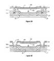
- FIGS. 5 A- 5 Eshow examples of cross-sections of varying implementations of interferometric modulators, including the movable reflective layer 14 and its supporting structures.
- FIG. 5Ashows an example of a partial cross-section of the interferometric modulator display of FIG. 1 , where a strip of metal material, i.e., the movable reflective layer 14 is deposited on supports 18 extending orthogonally from the substrate 20 .
- the movable reflective layer 14 of each IMODis generally square or rectangular in shape and attached to supports at or near the corners, on tethers 32 .
- FIG. 5Ashows an example of a partial cross-section of the interferometric modulator display of FIG. 1 , where a strip of metal material, i.e., the movable reflective layer 14 is deposited on supports 18 extending orthogonally from the substrate 20 .
- the movable reflective layer 14 of each IMODis generally square or rectangular in shape and attached to supports at or near the corners, on tethers
- the movable reflective layer 14is generally square or rectangular in shape and suspended from a deformable layer 34 , which may include a flexible metal.
- the deformable layer 34can connect, directly or indirectly, to the substrate 20 around the perimeter of the movable reflective layer 14 . These connections are herein referred to as support posts.
- the implementation shown in FIG. 5Chas additional benefits deriving from the decoupling of the optical functions of the movable reflective layer 14 from its mechanical functions, which are carried out by the deformable layer 34 . This decoupling allows the structural design and materials used for the reflective layer 14 and those used for the deformable layer 34 to be optimized independently of one another.
- FIG. 5Dshows another example of an IMOD, where the movable reflective layer 14 includes a reflective sub-layer 14 a .
- the movable reflective layer 14rests on a support structure, such as support posts 18 .
- the support posts 18provide separation of the movable reflective layer 14 from the lower stationary electrode (i.e., part of the optical stack 16 in the illustrated IMOD) so that a gap 19 is formed between the movable reflective layer 14 and the optical stack 16 , for example when the movable reflective layer 14 is in a relaxed position.
- the movable reflective layer 14also can include a conductive layer 14 c , which may be configured to serve as an electrode, and a support layer 14 b .
- the support layer 14 bcan be a stack of layers, such as, for example, a SiO 2 /SiON/SiO 2 tri-layer stack.
- Either or both of the reflective sub-layer 14 a and the conductive layer 14 ccan include, e.g., an Al alloy with about 0.5% Cu, or another reflective metallic material.
- Employing conductive layers 14 a , 14 c above and below the dielectric support layer 14 bcan balance stresses and provide enhanced conduction.
- the reflective sub-layer 14 a and the conductive layer 14 ccan be formed of different materials for a variety of design purposes, such as achieving specific stress profiles within the movable reflective layer 14 .
- some implementationsalso can include a black mask structure 23 .
- the black mask structure 23can be formed in optically inactive regions (e.g., between pixels or under posts 18 ) to absorb ambient or stray light.
- the black mask structure 23also can improve the optical properties of a display device by inhibiting light from being reflected from or transmitted through inactive portions of the display, thereby increasing the contrast ratio.
- the black mask structure 23can be conductive and be configured to function as an electrical bussing layer.
- the row electrodescan be connected to the black mask structure 23 to reduce the resistance of the connected row electrode.
- the black mask structure 23can be formed using a variety of methods, including deposition and patterning techniques.
- the black mask structure 23can include one or more layers.
- the black mask structure 23includes a molybdenum-chromium (MoCr) layer that serves as an optical absorber, a SiO 2 layer, and an aluminum alloy that serves as a reflector and a bussing layer, with a thickness in the range of about 30-80 ⁇ , 500-1000 ⁇ , and 500-6000 ⁇ , respectively.
- the one or more layerscan be patterned using a variety of techniques, including photolithography and dry etching, including, for example, CF 4 and/or O 2 for the MoCr and SiO 2 layers and Cl 2 and/or BCl 3 for the aluminum alloy layer.
- the black mask 23can be an etalon or interferometric stack structure.
- the conductive absorberscan be used to transmit or bus signals between lower, stationary electrodes in the optical stack 16 of each row or column.
- a spacer layer 35can serve to generally electrically isolate the absorber layer 16 a from the conductive layers in the black mask 23 .
- FIG. 5Eshows another example of an IMOD, where the movable reflective layer 14 is self supporting.
- the implementation of FIG. 5Edoes not include support posts 18 .
- the movable reflective layer 14contacts the underlying optical stack 16 at multiple locations, and the curvature of the movable reflective layer 14 provides sufficient support that the movable reflective layer 14 returns to the unactuated position of FIG. 5E when the voltage across the interferometric modulator is insufficient to cause actuation.
- the optical stack 16which may contain a plurality of several different layers, is shown here for clarity including an optical absorber 16 a , and a dielectric 16 b .
- the optical absorber 16 amay serve both as a fixed electrode and as a partially reflective layer.
- the IMODsfunction as direct-view devices, in which images are viewed from the front side of the transparent substrate 20 , i.e., the side opposite to that upon which the modulator is arranged.
- the back portions of the devicethat is, any portion of the display device behind the movable reflective layer 14 , including, for example, the deformable layer 34 illustrated in FIG. 5C
- the reflective layer 14optically shields those portions of the device.
- a bus structure(not illustrated) can be included behind the movable reflective layer 14 which provides the ability to separate the optical properties of the modulator from the electromechanical properties of the modulator, such as voltage addressing and the movements that result from such addressing.
- FIGS. 5A-5Ecan simplify processing, such as, e.g., patterning.
- FIG. 6shows an example of a flow diagram illustrating a manufacturing process 80 for an interferometric modulator
- FIGS. 7A-7Eshow examples of cross-sectional schematic illustrations of corresponding stages of such a manufacturing process 80 .
- the manufacturing process 80can be implemented to manufacture, e.g., interferometric modulators of the general type illustrated in FIGS. 1 and 5 , in addition to other blocks not shown in FIG. 6 .
- the process 80begins at block 82 with the formation of the optical stack 16 over the substrate 20 .
- FIG. 7Aillustrates such an optical stack 16 formed over the substrate 20 .
- the substrate 20may be a transparent substrate such as glass or plastic, it may be flexible or relatively stiff and unbending, and may have been subjected to prior preparation processes, e.g., cleaning, to facilitate efficient formation of the optical stack 16 .
- the optical stack 16can be electrically conductive, partially transparent and partially reflective and may be fabricated, for example, by depositing one or more layers having the desired properties onto the transparent substrate 20 .
- the optical stack 16includes a multilayer structure having sub-layers 16 a and 16 b , although more or fewer sub-layers may be included in some other implementations.
- one of the sub-layers 16 a , 16 bcan be configured with both optically absorptive and conductive properties, such as the combined conductor/absorber sub-layer 16 a . Additionally, one or more of the sub-layers 16 a , 16 b can be patterned into parallel strips, and may form row electrodes in a display device. Such patterning can be performed by a masking and etching process or another suitable process known in the art. In some implementations, one of the sub-layers 16 a , 16 b can be an insulating or dielectric layer, such as sub-layer 16 b that is deposited over one or more metal layers (e.g., one or more reflective and/or conductive layers). In addition, the optical stack 16 can be patterned into individual and parallel strips that form the rows of the display.
- the process 80continues at block 84 with the formation of a sacrificial layer 25 over the optical stack 16 .
- the sacrificial layer 25is later removed (e.g., at block 90 ) to form the cavity 19 and thus the sacrificial layer 25 is not shown in the resulting interferometric modulators 12 illustrated in FIG. 1 .
- FIG. 7Billustrates a partially fabricated device including a sacrificial layer 25 formed over the optical stack 16 .
- the formation of the sacrificial layer 25 over the optical stack 16may include deposition of a xenon difluoride (XeF 2 )-etchable material such as molybdenum (Mo) or amorphous silicon (Si), in a thickness selected to provide, after subsequent removal, a gap or cavity 19 (see also FIGS. 1 and 7E ) having a desired design size.
- XeF 2xenon difluoride
- Momolybdenum
- Siamorphous silicon
- Deposition of the sacrificial materialmay be carried out using deposition techniques such as physical vapor deposition (PVD, e.g., sputtering), plasma-enhanced chemical vapor deposition (PECVD), thermal chemical vapor deposition (thermal CVD), or spin-coating.
- PVDphysical vapor deposition
- PECVDplasma-enhanced chemical vapor deposition
- thermal CVDthermal chemical vapor deposition
- the process 80continues at block 86 with the formation of a support structure e.g., a post 18 as illustrated in FIGS. 1 , 5 and 7 C.
- the formation of the post 18may include patterning the sacrificial layer 25 to form a support structure aperture, then depositing a material (e.g., a polymer or an inorganic material, e.g., silicon oxide) into the aperture to form the post 18 , using a deposition method such as PVD, PECVD, thermal CVD, or spin-coating.
- a materiale.g., a polymer or an inorganic material, e.g., silicon oxide
- the support structure aperture formed in the sacrificial layercan extend through both the sacrificial layer 25 and the optical stack 16 to the underlying substrate 20 , so that the lower end of the post 18 contacts the substrate 20 as illustrated in FIG. 5A .
- the aperture formed in the sacrificial layer 25can extend through the sacrificial layer 25 , but not through the optical stack 16 .
- FIG. 7Eillustrates the lower ends of the support posts 18 in contact with an upper surface of the optical stack 16 .
- the post 18may be formed by depositing a layer of support structure material over the sacrificial layer 25 and patterning portions of the support structure material located away from apertures in the sacrificial layer 25 .
- the support structuresmay be located within the apertures, as illustrated in FIG. 7C , but also can, at least partially, extend over a portion of the sacrificial layer 25 .
- the patterning of the sacrificial layer 25 and/or the support posts 18can be performed by a patterning and etching process, but also may be performed by alternative etching methods.
- the process 80continues at block 88 with the formation of a movable reflective layer or membrane such as the movable reflective layer 14 illustrated in FIGS. 1 , 5 and 7 D.
- the movable reflective layer 14may be formed by employing one or more deposition steps, e.g., reflective layer (e.g., aluminum, aluminum alloy) deposition, along with one or more patterning, masking, and/or etching steps.
- the movable reflective layer 14can be electrically conductive, and referred to as an electrically conductive layer.
- the movable reflective layer 14may include a plurality of sub-layers 14 a , 14 b , 14 c as shown in FIG. 7D .
- one or more of the sub-layersmay include highly reflective sub-layers selected for their optical properties, and another sub-layer 14 b may include a mechanical sub-layer selected for its mechanical properties. Since the sacrificial layer 25 is still present in the partially fabricated interferometric modulator formed at block 88 , the movable reflective layer 14 is typically not movable at this stage. A partially fabricated IMOD that contains a sacrificial layer 25 may also be referred to herein as an “unreleased” IMOD. As described above in connection with FIG. 1 , the movable reflective layer 14 can be patterned into individual and parallel strips that form the columns of the display.
- the process 80continues at block 90 with the formation of a cavity, e.g., cavity 19 as illustrated in FIGS. 1 , 5 and 7 E.
- the cavity 19may be formed by exposing the sacrificial material 25 (deposited at block 84 ) to an etchant.
- an etchable sacrificial materialsuch as Mo or amorphous Si may be removed by dry chemical etching, e.g., by exposing the sacrificial layer 25 to a gaseous or vaporous etchant, such as vapors derived from solid XeF 2 for a period of time that is effective to remove the desired amount of material, typically selectively removed relative to the structures surrounding the cavity 19 .
- Other etching methodse.g.
- the movable reflective layer 14is typically movable after this stage. After removal of the sacrificial material 25 , the resulting fully or partially fabricated IMOD may be referred to herein as a “released” IMOD.
- the display 100has a body 101 , a major surface 102 and a reflective surface 103 .
- the body 101is transmissive to desired wavelengths of radiation, e.g., wavelengths of light in the visible spectrum, and may be a transparent substrate such as the substrate 20 in, e.g., FIG. 1 .
- the body 101can be discontinuous, e.g., have gaps, and/or may be formed of multiple layers of material.
- the major surface 102faces a viewer 104 and is typically flat, as illustrated. In use, the viewer 104 typically perceives an image as being displayed on the major surface 102 , although the display elements forming the image may be below the surface 102 .
- the reflective surface 103is configured to reflect light out of the body 101 towards the viewer 104 .
- This reflective surface 103may be continuous or discontinuous.
- the reflective surface 103may be formed of a continuous layer of material, or may be a part of devices such as interferometric modulators.
- the surface 103may include reflective layer 14 of interferometric modulators 12 in, e.g., FIG. 1 .
- the display 100whether having display elements formed of interferometric modulators or other devices, has a range of viewing directions within which display performance can be specified as acceptable. This range of directions is referred to as a view cone 110 .
- the imagecan be unacceptably distorted or can contain an unacceptable number of artifacts when viewed from directions outside of the view cone 110 .
- interferometric modulators 12have posts 18 , which can cause shadows and can block light at some viewing angles, thereby causing non-uniformities across the display 100 .
- the view cone 110includes viewing directions within about ⁇ 60°, about ⁇ 45°, about ⁇ 30°, about ⁇ 25°, about ⁇ 15°, about ⁇ 10°, or about ⁇ 5° of an axis 105 extending out from the major surface 102 of the display. Larger angles for the view cone 110 may allow for a larger range of viewing angles for a viewer, and smaller viewer angles may allow for a greater apparent brightness, since light from many different directions can be focused within a relatively small view cone 110 . As illustrated, this axis 105 can be configured normal to the major surface 102 . In some other arrangements, however, the view cone 110 may be centered on an axis (not shown) that is tilted relative to the normal.
- the view cone 110may be in the shape of a symmetrical cone having a boundary that extends at an angle of about ⁇ 60°, about ⁇ 45°, about ⁇ 30°, about ⁇ 25°, about ⁇ 15°, about ⁇ 10°, or about ⁇ 5° relative to the normal.
- the view cone 110can have a tip at the intersection point of the normal 105 and the major surface 102 and can be rotated, at an angle of about ⁇ 60°, or about ⁇ 45°, about the axis 105 defined by the normal. It will be appreciated that, even within the view cone 110 , the image quality may vary somewhat depending upon viewing direction; there may be a subset of viewing directions with which superior image quality is observed.
- the display 100uses reflected light to produce an image.
- the reflected light that is directed towards a viewer 104 within the view cone 110can determine the perceived brightness of the display 100 .
- some of the light striking the displayis “useful” in that it is reflected and propagates away from the display 100 within the view cone 110 .
- some of the lightis “non-useful” in that it is not reflected within the view cone 110 .
- the angles at which the non-useful light impinges on the display 100may be referred to as “non-useful” angles.
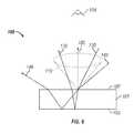
- FIG. 8Useful and non-useful light are illustrated in FIG. 8 .
- rays of lightare reflected differently and propagate away from the display 100 at different angles.
- rays incident on the surface 102 at angles within the view conemay be reflected out of the display 100 at angles that are also within the view cone 110 .
- ray 130is incident on the surface 102 at an angle within the view cone 110 .
- the ray 130passes into the body 101 and continues to propagate through the body 101 until it contacts the reflective surface 103 , which reflects the ray 130 back out of the body 101 .
- the ray 130exits the body 101 and propagates away from the display 100 within the view cone 110 .
- rays of lightmay be incident on the body 101 at angles that are outside of the view cone 110 .
- ray 140is incident on the body 101 at an angle outside of the view cone 110 .
- the ray 140passes into the body 101 , and is reflected out of the body 101 by the reflective surface 103 .
- Rays such as the ray 140are non-useful light for image formation purposes since they are not reflected out of the display 100 within the view cone 110 . As a result, such rays are not perceived by the viewer 104 as contributing to the brightness of an image shown on the display 100 .
- non-useful lightcan be captured and converted into useful light.
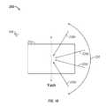
- FIG. 9an example of a cross section of a portion of a display 200 is schematically illustrated.
- the display 200includes the body 101 , the major surface 102 , the reflective surface 103 , and the view cone 110 as discussed with respect to FIG. 8 .
- the hologram 212is configured, or recorded, so that light turning features constituting the hologram 212 turn light from non-useful angles such that, after being turned, this light passes into the body 101 and is then reflected and propagates away from the display 200 within the view cone 110 ; that is, the reflected light exits the display 200 at an angle that is within the view cone 110 .
- Light ray 220is an example of non-useful light that is turned by the hologram 212 and made useful.
- the light ray 220is incident on the holographic element 210 at an angle 222 from the axis 105 that is outside of the view cone 110 ; that is, outside of the range of angles encompassed by the view cone 110 .
- the ray 220may be incident on the holographic film 210 at an angle of 222 , which is depicted greater than about 45° relative to the axis 105 .
- the angle 222may be greater than about 60° relative to the axis 105 , or the normal.
- the ray 220passes into the holographic element 210 and is diffracted by the hologram 212 to such a degree that the ray 220 passes into the body 101 and continues to the reflective surface 103 , where it is reflected and directed out of the display 200 at an angle 224 from the normal that is within the view cone 110 ; that is, within the range of angles encompassed by the view cone 110 .
- the angle 224is within a range of about ⁇ 60°, or about ⁇ 45°, relative to the normal to the major surface 102 .
- FIG. 10illustrates an example of a top-down plan view of a portion of the display 200 .
- the ray 220can be incident on the holographic element 210 from multiple different directions.
- the angle 222 in FIG. 9 relative to the axis 105can vary.
- the angles made by non-useful incident rays 220 a - 220 d on the x-y planecan vary.
- the rays 220 a - 220 dcan impinge on the holographic element 210 from a range of angles 230 relative to, e.g., the y-axis.
- hologramstypically are most efficient at turning light from a single direction, since holograms are typically formed by light striking a holographic film from one direction.
- the hologram 212( FIG. 9 ) is most efficient at turning light from that one direction. Light incident on the hologram 212 from directions different from that one direction may be turned with a relatively low turning efficiency and the turning of that light may also cause color shifts.
- the hologram 212is configured to turn light impinging on the holographic element 210 from multiple directions. It will be appreciated that the hologram 212 may be formed by striking a holographic film with light rays that converge in the body of the film. In some implementations, the hologram 212 is formed using a first set of light sources, arrayed at a plurality of directions around a holographic film. A second set of one or more light sources directs light into the holographic film so that the light rays from that second set are, e.g., from the direction of the viewer (e.g., normal to the major surface of the holographic film).
- a hologramis formed at the convergence of the light from the first and second sets of light sources.
- the angles that the light from the first set of light sources form when impinging on the holographic filmcorrespond to the angles of the light that the holographic film is configured to turn.
- one or a limited number of light sourcescan be passed through a diffuser to form the hologram 212 ; the diffuser can cause light to strike the holographic film at different angles.
- the light spectrum of the light sources used to form the hologram 212may be selected to form a hologram that will turn light within a desired wavelength range (e.g., within the visible spectrum). This may be accomplished by appropriate selection of the wavelengths of light used to form the hologram 212 .
- the wavelengths of light used to form the hologram 212are the same as the wavelengths of light that the hologram 212 is configured to turn.
- the hologram 212can be configured to turn light of only one wavelength, if desired.
- the hologram 212may be configured to turn light of a desired range of wavelengths and from a desired number of directions.
- the hologram 212can be pixilated.
- the individual pixelscan be configured to turn light of different wavelengths and/or from different directions.
- FIG. 11illustrates an example of a top-down plan view of a portion of the hologram 212 .
- the hologram 212is provided with a plurality of separated and non-overlapping pixels 212 i+n . Individual ones of the pixels 212 i+n are configured to turn light incident on the hologram 212 from one particular direction. Each individual one of the pixels 212 i+n can be further configured to turn light of one particular wavelength.
- the wavelengths of lightcan correspond to the individual colors produced by individual display elements of the display 200 .
- the pixels 212 i+nare configured to turn light corresponding to the colors red, green and blue. Some pixels configured to turn light corresponding to different colors or oriented to turn light from different directions are indicated by reference numerals 212 i , 212 i+1 , 212 i+2 , 212 i+3 .
- the relative number of pixels of each type of pixelallows the response of the hologram to be tailored for the display. For example, in some applications, light may be expected to come from a limited number of directions. To turn a high proportion of the light from those directions, the population of pixels 212 i+n may contain a larger number or surface area of pixels configured to turn light from those particular directions than from any other directions, or the pixels may only turn light from those directions.
- the pixels 212 i+nmay have a uniform density of similar pixels (or pixels of similar total surface area) configured to turn light from a uniform distribution of different desired directions. This uniformity in the light turning properties of the pixels 212 i+n incident on the display 200 improves the brightness uniformity of the display 200 as it is moved in normal operation.
- the pixels 212 i+nmay be used to adjust the color balance of the display 200 .
- the number or surface area of pixels 212 i+n that turn one or more colorscan be increased to increase the intensity of the one or colors in images produced by the display 200 .
- the proportion of red light turned by the hologram 212can be increased in displays that produce the color red at lower intensities than other colors. This increase in the intensity of the color red can be achieved by increasing the number or surface area of pixels 212 i+n that turn light corresponding to the color red, relative to pixels that turn light of other colors.
- the intensity of one or more particular colorscan be reduced by providing a lower number or surface area of pixels 212 i+n that turn light of those colors, relative to pixels 212 i+n that turn light of other colors.
- the relative surface area of a set of pixelscan be changed by changing the absolute number of those pixels relative to other pixels, or the relative sizes of the pixels can be changed to achieve a desired total surface area for a particular type of pixel.
- the pixels 212 i+nmay be formed by various methods, such as by using a mask with openings that allow illumination of selected portions of the holographic film in a first position, and shifting the mask to other positions, e.g., second and third other positions, etc., and exposing the holographic film to light while the mask is in each position.
- a mask with openingsthat allow illumination of selected portions of the holographic film in a first position
- other positionse.g., second and third other positions, etc.
- exposing the holographic film to light while the mask is in each positione.g., an array of regularly repeating, discrete regions configured to turn light from a particular direction and at a particular wavelength may be formed.
- Each discrete regioncan constitute a pixel in the hologram.
- the holographic filmcan be exposed to laser light of a different wavelength and/or direction. The wavelength corresponds to the wavelength of light that the pixel is configured to turn.
- the laser lightcan include laser beams oriented substantially normal to the holographic film.
- a secondary beamwhich can have the same wavelength as the substantially normal laser beam, can be directed into the holographic film at the same direction as light to be turned by the hologram.
- the range of light rays that the hologram 212 is configured to turnmay be limited.
- the hologram 212may be configured to turn light from a limited range of angles relative to the z-axis 105 or normal as in FIG. 9 and/or a limited range of angles relative to the y-axis as in FIG. 10 .
- lightmay impinge on the hologram 210 from a range of directions which can have azimuths on the plane of the hologram 210 .
- these azimuthscan vary in a range from 0-360°.
- the rays 220 a - 220 dcorrespond to the azimuths and the range of angles 230 over which the rays 220 a - 220 d extend can be limited to, e.g., a range of about 270° or about 180° as viewed on the x-y plane on which is the major surface 102 ( FIG. 9 ) or the holographic is disposed.
- the azimuths for light turned by the hologramcan extend in a range of about 0-270° or about 0-180°. Due to the configuration (e.g., positions of control and input devices) of devices containing the display 200 , the viewer 104 and ambient light sources will typically be positioned at a predetermined position relative to the display 200 . For example, where the display is part of a hand-held device, or upright display (e.g., a monitor), it is possible that the device will be positioned with one end of the display 200 pointed upwards, such as towards the sky.
- the hologram 212may be configured to turn light coming from directions at one end of the display 200 (e.g., which may be expected to point towards ambient light sources), but not light coming from the direction of the opposite end of the display (e.g., which may be expected to point towards the ground, away from ambient light sources).
- a first set of directions for which the hologram 212 is configured to turn lightspans about 180° on the x-y plane of the display 200 and the hologram 212 is not configured to turn light, or configured to not turn light, incident on the display 200 from other directions opposite that first set of directions.
- the angles which the hologram 212 is not configured to turn lightcorrespond to those directions that are not expected to point towards an ambient light source.
- the hologram 212can be configured to turn ambient light so that it reflects off the reflective surface 103 such that the reflected light propagates away from the display 200 at multiple different angles within the view cone 110 .
- the hologram 212can be configured to turn those light rays such that each is reflected and propagates away from the display 200 at one of a plurality of different angles within the view cone 110 .
- the set of pixels 212 i+n configured to turn light coming from a single directionalso can contain multiple sub-sets of pixels, with each sub-set configured to turn light into the body 101 at a different angle from that of other sub-sets, so that the light from that single direction is reflected and propagates away from the display 200 at a different angle from that of other subsets.
- Such an arrangementcan increase the brightness uniformity of images as the viewing angle changes within the view cone 110 .
- the holographic element 210has been illustrated as the uppermost part of the device 200 for ease of illustration and discussion.
- Other materialsmay be disposed over the holographic element 210 .
- anti-reflective and/or scratch-resistant layersmay be provided over the holographic element 210 .
- other materialsmay be provided between the holographic element 210 and the body 101 .
- individual pixels 212 i+nalso can be configured to turn light of one or more different wavelengths and/or one or more different directions.
- the efficiency of light turningdecreases as an individual pixel 212 i+n is made to turn light of more directions or wavelengths, the number of directions and the number of colors can be limited to one.
- FIGS. 12A and 12Bshow examples of system block diagrams illustrating a display device 40 that includes a plurality of interferometric modulators.
- the display device 40can be, for example, a cellular or mobile telephone.
- the same components of the display device 40 or slight variations thereofare also illustrative of various types of display devices such as televisions, e-readers and portable media players.
- the display device 40includes a housing 41 , a display 30 , an antenna 43 , a speaker 45 , an input device 48 , and a microphone 46 .
- the housing 41can be formed from any of a variety of manufacturing processes, including injection molding, and vacuum forming.
- the housing 41may be made from any of a variety of materials, including, but not limited to: plastic, metal, glass, rubber, and ceramic, or a combination thereof.
- the housing 41can include removable portions (not shown) that may be interchanged with other removable portions of different color, or containing different logos, pictures, or symbols.
- the display 30may be any of a variety of displays, including a bi-stable or analog display, as described herein.
- the display 30also can be configured to include a flat-panel display, such as plasma, EL, OLED, STN LCD, or TFT LCD, or a non-flat-panel display, such as a CRT or other tube device.
- the display 30can include an interferometric modulator display, as described herein.
- the components of the display device 40are schematically illustrated in FIG. 12B .
- the display device 40includes a housing 41 and can include additional components at least partially enclosed therein.
- the display device 40includes a network interface 27 that includes an antenna 43 which is coupled to a transceiver 47 .
- the transceiver 47is connected to a processor 21 , which is connected to conditioning hardware 52 .
- the conditioning hardware 52may be configured to condition a signal (e.g., filter a signal).
- the conditioning hardware 52is connected to a speaker 45 and a microphone 46 .
- the processor 21is also connected to an input device 48 and a driver controller 29 .
- the driver controller 29is coupled to a frame buffer 28 , and to an array driver 22 , which in turn is coupled to a display array 30 .
- a power supply 50can provide power to all components as required by the particular display device 40 design.
- the network interface 27includes the antenna 43 and the transceiver 47 so that the display device 40 can communicate with one or more devices over a network.
- the network interface 27also may have some processing capabilities to relieve, e.g., data processing requirements of the processor 21 .
- the antenna 43can transmit and receive signals.
- the antenna 43transmits and receives RF signals according to the IEEE 16.11 standard, including IEEE 16.11(a), (b), or (g), or the IEEE 802.11 standard, including IEEE 802.11a, b, g or n.
- the antenna 43transmits and receives RF signals according to the BLUETOOTH standard.
- the antenna 43is designed to receive code division multiple access (CDMA), frequency division multiple access (FDMA), time division multiple access (TDMA), Global System for Mobile communications (GSM), GSM/General Packet Radio Service (GPRS), Enhanced Data GSM Environment (EDGE), Terrestrial Trunked Radio (TETRA), Wideband-CDMA (W-CDMA), Evolution Data Optimized (EV-DO), 1xEV-DO, EV-DO Rev A, EV-DO Rev B, High Speed Packet Access (HSPA), High Speed Downlink Packet Access (HSDPA), High Speed Uplink Packet Access (HSUPA), Evolved High Speed Packet Access (HSPA+), Long Term Evolution (LTE), AMPS, or other known signals that are used to communicate within a wireless network, such as a system utilizing 3G or 4G technology.
- CDMAcode division multiple access
- FDMAfrequency division multiple access
- TDMATime division multiple access
- GSMGlobal System for Mobile communications
- GPRSGSM/General Packet
- the transceiver 47can pre-process the signals received from the antenna 43 so that they may be received by and further manipulated by the processor 21 .
- the transceiver 47also can process signals received from the processor 21 so that they may be transmitted from the display device 40 via the antenna 43 .
- the transceiver 47can be replaced by a receiver.
- the network interface 27can be replaced by an image source, which can store or generate image data to be sent to the processor 21 .
- the processor 21can control the overall operation of the display device 40 .
- the processor 21receives data, such as compressed image data from the network interface 27 or an image source, and processes the data into raw image data or into a format that is readily processed into raw image data.
- the processor 21can send the processed data to the driver controller 29 or to the frame buffer 28 for storage.
- Raw datatypically refers to the information that identifies the image characteristics at each location within an image. For example, such image characteristics can include color, saturation, and gray-scale level.
- the processor 21can include a microcontroller, CPU, or logic unit to control operation of the display device 40 .
- the conditioning hardware 52may include amplifiers and filters for transmitting signals to the speaker 45 , and for receiving signals from the microphone 46 .
- the conditioning hardware 52may be discrete components within the display device 40 , or may be incorporated within the processor 21 or other components.
- the driver controller 29can take the raw image data generated by the processor 21 either directly from the processor 21 or from the frame buffer 28 and can re-format the raw image data appropriately for high speed transmission to the array driver 22 .
- the driver controller 29can re-format the raw image data into a data flow having a raster-like format, such that it has a time order suitable for scanning across the display array 30 . Then the driver controller 29 sends the formatted information to the array driver 22 .
- a driver controller 29such as an LCD controller, is often associated with the system processor 21 as a stand-alone Integrated Circuit (IC), such controllers may be implemented in many ways.
- controllersmay be embedded in the processor 21 as hardware, embedded in the processor 21 as software, or fully integrated in hardware with the array driver 22 .
- the array driver 22can receive the formatted information from the driver controller 29 and can re-format the video data into a parallel set of waveforms that are applied many times per second to the hundreds, and sometimes thousands (or more), of leads coming from the display's x-y matrix of pixels.
- the driver controller 29 , the array driver 22 , and the display array 30are appropriate for any of the types of displays described herein.
- the driver controller 29can be a conventional display controller or a bi-stable display controller (e.g., an IMOD controller).
- the array driver 22can be a conventional driver or a bi-stable display driver (e.g., an IMOD display driver).
- the display array 30can be a conventional display array or a bi-stable display array (e.g., a display including an array of IMODs).
- the driver controller 29can be integrated with the array driver 22 . Such an implementation is common in highly integrated systems such as cellular phones, watches and other small-area displays.
- the input device 48can be configured to allow, e.g., a user to control the operation of the display device 40 .
- the input device 48can include a keypad, such as a QWERTY keyboard or a telephone keypad, a button, a switch, a rocker, a touch-sensitive screen, or a pressure- or heat-sensitive membrane.
- the microphone 46can be configured as an input device for the display device 40 . In some implementations, voice commands through the microphone 46 can be used for controlling operations of the display device 40 .
- the power supply 50can include a variety of energy storage devices as are well known in the art.
- the power supply 50can be a rechargeable battery, such as a nickel-cadmium battery or a lithium-ion battery.
- the power supply 50also can be a renewable energy source, a capacitor, or a solar cell, including a plastic solar cell or solar-cell paint.
- the power supply 50also can be configured to receive power from a wall outlet.
- control programmabilityresides in the driver controller 29 which can be located in several places in the electronic display system. In some other implementations, control programmability resides in the array driver 22 .
- the above-described optimizationmay be implemented in any number of hardware and/or software components and in various configurations.
- the hardware and data processing apparatus used to implement the various illustrative logics, logical blocks, modules and circuits described in connection with the aspects disclosed hereinmay be implemented or performed with a general purpose single- or multi-chip processor, a digital signal processor (DSP), an application specific integrated circuit (ASIC), a field programmable gate array (FPGA) or other programmable logic device, discrete gate or transistor logic, discrete hardware components, or any combination thereof designed to perform the functions described herein.
- a general purpose processormay be a microprocessor, or, any conventional processor, controller, microcontroller, or state machine.
- a processormay also be implemented as a combination of computing devices, e.g., a combination of a DSP and a microprocessor, a plurality of microprocessors, one or more microprocessors in conjunction with a DSP core, or any other such configuration.
- particular steps and methodsmay be performed by circuitry that is specific to a given function.
- the functions describedmay be implemented in hardware, digital electronic circuitry, computer software, firmware, including the structures disclosed in this specification and their structural equivalents thereof, or in any combination thereof. Implementations of the subject matter described in this specification also can be implemented as one or more computer programs, i.e., one or more modules of computer program instructions, encoded on a computer storage media for execution by, or to control the operation of, data processing apparatus.
Landscapes
- Physics & Mathematics (AREA)
- General Physics & Mathematics (AREA)
- Optics & Photonics (AREA)
- Spectroscopy & Molecular Physics (AREA)
- Mechanical Light Control Or Optical Switches (AREA)
Abstract
Description
Claims (31)
Priority Applications (2)
| Application Number | Priority Date | Filing Date | Title |
|---|---|---|---|
| US12/969,224US8902484B2 (en) | 2010-12-15 | 2010-12-15 | Holographic brightness enhancement film |
| PCT/US2011/064482WO2012082651A1 (en) | 2010-12-15 | 2011-12-12 | Holographic brightness enhancement film |
Applications Claiming Priority (1)
| Application Number | Priority Date | Filing Date | Title |
|---|---|---|---|
| US12/969,224US8902484B2 (en) | 2010-12-15 | 2010-12-15 | Holographic brightness enhancement film |
Publications (2)
| Publication Number | Publication Date |
|---|---|
| US20120154881A1 US20120154881A1 (en) | 2012-06-21 |
| US8902484B2true US8902484B2 (en) | 2014-12-02 |
Family
ID=45531528
Family Applications (1)
| Application Number | Title | Priority Date | Filing Date |
|---|---|---|---|
| US12/969,224Expired - Fee RelatedUS8902484B2 (en) | 2010-12-15 | 2010-12-15 | Holographic brightness enhancement film |
Country Status (2)
| Country | Link |
|---|---|
| US (1) | US8902484B2 (en) |
| WO (1) | WO2012082651A1 (en) |
Families Citing this family (6)
| Publication number | Priority date | Publication date | Assignee | Title |
|---|---|---|---|---|
| TWI289708B (en) | 2002-12-25 | 2007-11-11 | Qualcomm Mems Technologies Inc | Optical interference type color display |
| EP1943555B1 (en) | 2006-10-06 | 2012-05-02 | QUALCOMM MEMS Technologies, Inc. | Optical loss structure integrated in an illumination apparatus of a display |
| EP1943551A2 (en) | 2006-10-06 | 2008-07-16 | Qualcomm Mems Technologies, Inc. | Light guide |
| US8068710B2 (en) | 2007-12-07 | 2011-11-29 | Qualcomm Mems Technologies, Inc. | Decoupled holographic film and diffuser |
| US8902484B2 (en) | 2010-12-15 | 2014-12-02 | Qualcomm Mems Technologies, Inc. | Holographic brightness enhancement film |
| US20230050198A1 (en)* | 2020-01-20 | 2023-02-16 | Vuzix Corporation | Near-eye display based on conical diffraction |
Citations (686)
| Publication number | Priority date | Publication date | Assignee | Title |
|---|---|---|---|---|
| US2518647A (en) | 1948-01-07 | 1950-08-15 | Celanese Corp | Interferometer means for thickness measurements |
| US3813265A (en) | 1970-02-16 | 1974-05-28 | A Marks | Electro-optical dipolar material |
| US3924929A (en) | 1966-11-14 | 1975-12-09 | Minnesota Mining & Mfg | Retro-reflective sheet material |
| US4154219A (en) | 1977-03-11 | 1979-05-15 | E-Systems, Inc. | Prismatic solar reflector apparatus and method of solar tracking |
| US4375312A (en) | 1980-08-07 | 1983-03-01 | Hughes Aircraft Company | Graded index waveguide structure and process for forming same |
| US4378567A (en) | 1981-01-29 | 1983-03-29 | Eastman Kodak Company | Electronic imaging apparatus having means for reducing inter-pixel transmission nonuniformity |
| DE3402746A1 (en) | 1984-01-27 | 1985-08-08 | Robert Bosch Gmbh, 7000 Stuttgart | Liquid crystal display |
| JPS60242408A (en) | 1984-05-17 | 1985-12-02 | Seiko Epson Corp | Light source optical system for light guide |
| JPS629317Y2 (en) | 1982-09-13 | 1987-03-04 | ||
| EP0278038A1 (en) | 1987-02-13 | 1988-08-17 | Battelle-Institut e.V. | Active flat type display panel |
| US4832459A (en) | 1984-02-06 | 1989-05-23 | Rogers Corporation | Backlighting for electro-optical passive displays and transflective layer useful therewith |
| US4850682A (en) | 1986-07-14 | 1989-07-25 | Advanced Environmental Research Group | Diffraction grating structures |
| US4863224A (en) | 1981-10-06 | 1989-09-05 | Afian Viktor V | Solar concentrator and manufacturing method therefor |
| US4915479A (en) | 1986-12-17 | 1990-04-10 | U.S. Philips Corporation | Liquid crystal display illumination system |
| US4918577A (en) | 1988-01-16 | 1990-04-17 | Alps Electric Co., Ltd. | Illumination light transmitting device |
| US4947291A (en) | 1988-06-17 | 1990-08-07 | Mcdermott Kevin | Lighting device |
| EP0389031A1 (en) | 1989-03-16 | 1990-09-26 | Koninklijke Philips Electronics N.V. | Colour display device |
| US4961617A (en) | 1989-07-19 | 1990-10-09 | Ferrydon Shahidi | Fibre optic waveguide illuminating elements |
| US5038224A (en) | 1989-12-22 | 1991-08-06 | Bell Communications Research, Inc. | Video imaging device in a teleconferencing system |
| US5042921A (en) | 1988-10-25 | 1991-08-27 | Casio Computer Co., Ltd. | Liquid crystal display apparatus |
| US5050946A (en) | 1990-09-27 | 1991-09-24 | Compaq Computer Corporation | Faceted light pipe |
| US5110370A (en) | 1990-09-20 | 1992-05-05 | United Solar Systems Corporation | Photovoltaic device with decreased gridline shading and method for its manufacture |
| US5123247A (en) | 1990-02-14 | 1992-06-23 | 116736 (Canada) Inc. | Solar roof collector |
| US5151585A (en) | 1991-08-12 | 1992-09-29 | Hughes Danbury Optical Systems, Inc. | Coherent radiation detector |
| JPH0481816B2 (en) | 1985-08-26 | 1992-12-25 | Matsushita Electric Ind Co Ltd | |
| EP0539099A2 (en) | 1991-10-25 | 1993-04-28 | Optical Coating Laboratory, Inc. | Repositionable optical cover for monitors |
| US5226099A (en) | 1991-04-26 | 1993-07-06 | Texas Instruments Incorporated | Digital micromirror shutter device |
| JPH05281479A (en) | 1992-03-31 | 1993-10-29 | Nippon Steel Corp | Display device |
| US5261970A (en) | 1992-04-08 | 1993-11-16 | Sverdrup Technology, Inc. | Optoelectronic and photovoltaic devices with low-reflectance surfaces |
| US5272496A (en) | 1991-08-06 | 1993-12-21 | Thomson-Csf | Image projector with optimized luminous efficiency |
| US5278680A (en) | 1989-10-05 | 1994-01-11 | Seiko Epson Corporation | Projection type liquid crystal display system and method of polarized light component projection |
| US5283600A (en) | 1992-02-21 | 1994-02-01 | Nec Corporation | LCD projector |
| US5289300A (en) | 1991-02-04 | 1994-02-22 | Semiconductor Energy Laboratory Co., Ltd. | Method of manufacturing electro-optical devices wherein the electrode is patterned on the modulation layer |
| WO1994006871A1 (en) | 1992-09-17 | 1994-03-31 | Canterbury Park Limited | A sign, a method of making the sign and an ink therefor |
| EP0590511A1 (en) | 1992-10-01 | 1994-04-06 | International Business Machines Corporation | Edge-lit transflective non-emissive display |
| GB2260203B (en) | 1991-10-04 | 1994-09-07 | Marconi Gec Ltd | Colour display system |
| EP0621500A1 (en) | 1993-04-23 | 1994-10-26 | AT&T Corp. | Illuminated transparent display with microtextured back reflector |
| US5361190A (en) | 1990-02-20 | 1994-11-01 | K. W. Muth Co. Inc. | Mirror assembly |
| GB2278222A (en) | 1993-05-20 | 1994-11-23 | Sharp Kk | Spatial light modulator |
| WO1995001584A1 (en) | 1993-07-01 | 1995-01-12 | Alliedsignal Inc. | Direct view display device with array of tapered waveguide |
| US5387953A (en) | 1990-12-27 | 1995-02-07 | Canon Kabushiki Kaisha | Polarization illumination device and projector having the same |
| US5387991A (en) | 1990-05-18 | 1995-02-07 | Canon Kabushiki Kaisha | Polarization converting device and polarized-light illuminating system using the device and image display unit using the device |
| US5398125A (en) | 1993-11-10 | 1995-03-14 | Minnesota Mining And Manufacturing Company | Liquid crystal projection panel having microlens arrays, on each side of the liquid crystal, with a focus beyond the liquid crystal |
| WO1995014256A1 (en) | 1993-11-15 | 1995-05-26 | Alliedsignal Inc. | Optical element for use in an array of optical elements in a display arrangement |
| WO1995015582A1 (en) | 1993-12-02 | 1995-06-08 | R & S Renewable Energy Systems B.V. | A photovoltaic solar panel and a method for producing same |
| US5446510A (en) | 1989-12-20 | 1995-08-29 | Canon Kabushiki Kaisha | Image display apparatus |
| US5448659A (en) | 1993-02-01 | 1995-09-05 | Matsushita Electric Industrial Co., Ltd. | Waveguide-type image transmission device and fingerprint identification device |
| US5452385A (en) | 1993-03-09 | 1995-09-19 | Sharp Kabushiki Kaisha | Optical scanning device an optical scanning type display and an image data input/output device |
| US5459610A (en) | 1992-04-28 | 1995-10-17 | The Board Of Trustees Of The Leland Stanford, Junior University | Deformable grating apparatus for modulating a light beam and including means for obviating stiction between grating elements and underlying substrate |
| US5467417A (en) | 1992-09-16 | 1995-11-14 | Hitachi, Ltd. | Prism plate for efficiently emitting light flux within a predetermined range, and liquid crystal indicator and indicator illumination method using the same |
| US5515184A (en) | 1991-11-12 | 1996-05-07 | The University Of Alabama In Huntsville | Waveguide hologram illuminators |
| US5517366A (en) | 1993-10-22 | 1996-05-14 | Olympus Optical Co., Ltd. | Concentric optical system |
| WO1996016348A1 (en) | 1994-11-24 | 1996-05-30 | Hitachi Ltd. | Liquid crystal display device |
| US5555186A (en) | 1994-02-15 | 1996-09-10 | Nec Corporation | Projection type liquid crystal display apparatus using multiple polarizing beam splitters |
| US5555160A (en) | 1991-06-27 | 1996-09-10 | Nissen Chemitec Co., Ltd. | Light-guiding panel for surface lighting and a surface lighting body |
| US5592332A (en) | 1992-12-25 | 1997-01-07 | Dai Nippon Printing Co., Ltd. | Renticular lens, surface light source, and liquid crystal display apparatus |
| WO1997001240A1 (en) | 1995-06-20 | 1997-01-09 | Thomson Consumer Electronics, Inc. | Back lit electronic viewfinder |
| JPH095735A (en) | 1995-06-21 | 1997-01-10 | Hitachi Ltd | Reflective liquid crystal display |
| US5594830A (en) | 1992-03-23 | 1997-01-14 | Minnesota Mining And Manufacturing Co. | Luminaire device |
| JPH0922012A (en) | 1995-07-06 | 1997-01-21 | Mitsubishi Rayon Co Ltd | Backlight and liquid crystal display device using the same |
| US5601351A (en) | 1994-06-01 | 1997-02-11 | U.S. Philips Corporation | High-efficiency illumination device and image projection apparatus comprising such a device |
| US5626408A (en) | 1993-12-17 | 1997-05-06 | U.S. Philips Corporation | Illumination system for a color projection device and circular polarizer suitable for use in such an illumination system, and color image projection device comprising such an illumination system and circular polarizer |
| WO1997016756A1 (en) | 1995-11-01 | 1997-05-09 | Matsushita Electric Industrial Co., Ltd. | Outgoing efficiency control device, projection type display apparatus, infrared sensor and non-contact thermometer |
| US5638084A (en) | 1992-05-22 | 1997-06-10 | Dielectric Systems International, Inc. | Lighting-independent color video display |
| JPH09160032A (en) | 1995-12-12 | 1997-06-20 | Omron Corp | Illuminator, liquid crystal display device using the illuminator, portable terminal equipment, on board equipment and optical recognition device |
| US5647036A (en) | 1994-09-09 | 1997-07-08 | Deacon Research | Projection display with electrically-controlled waveguide routing |
| JPH09178949A (en) | 1995-12-25 | 1997-07-11 | Sharp Corp | Flat lighting device |
| US5650865A (en) | 1995-03-21 | 1997-07-22 | Hughes Electronics | Holographic backlight for flat panel displays |
| US5659410A (en) | 1993-12-28 | 1997-08-19 | Enplas Corporation | Surface light source device and liquid crystal display |
| US5664862A (en) | 1994-11-29 | 1997-09-09 | Precision Lamp, Inc. | Edge light for panel display |
| US5671314A (en) | 1993-01-15 | 1997-09-23 | Sisters Of Prividence In Oregon | Illuminator devices for ultraviolet light delivery and methods of making same |
| US5673128A (en) | 1995-01-31 | 1997-09-30 | Sharp Kabushiki Kaisha | Back light device of liquid crystal device |
| US5671994A (en) | 1994-06-08 | 1997-09-30 | Clio Technologies, Inc. | Flat and transparent front-lighting system using microprisms |
| JPH09307140A (en) | 1996-05-14 | 1997-11-28 | Matsushita Electron Corp | Semiconductor light emitting device |
| JPH09311333A (en) | 1996-05-17 | 1997-12-02 | Matsushita Electric Ind Co Ltd | Lighting device for reflective display and reflective liquid crystal display device |
| WO1997046908A1 (en) | 1996-06-05 | 1997-12-11 | Forschungszentrum Jülich GmbH | Interference filter based on porous silicon |
| US5703667A (en) | 1996-05-31 | 1997-12-30 | Shimada Precision, Co., Ltd. | Light guide plates and light guide plate assembly utilizing diffraction grating |
| US5712694A (en) | 1994-09-16 | 1998-01-27 | Kabushiki Kaisha Toshiba | LCD comprising a light separating element including a cholesteric liquid crystal sheet |
| GB2315356A (en) | 1996-07-15 | 1998-01-28 | Lg Electronics Inc | Liquid crystal display with microlenses |
| EP0822441A2 (en) | 1996-08-01 | 1998-02-04 | Sharp Kabushiki Kaisha | Optical device and directional display |
| US5735590A (en) | 1994-03-02 | 1998-04-07 | Tosoh Corporation | Backlighting device with a transparent sheet having straight ridges |
| WO1998019201A1 (en) | 1996-10-29 | 1998-05-07 | Xeotron Corporation | Optical device utilizing optical waveguides and mechanical light-switches |
| US5749642A (en) | 1992-03-18 | 1998-05-12 | Canon Kabushiki Kaisha | Illuminating optical system and projector utilizing the same |
| US5771124A (en) | 1996-07-02 | 1998-06-23 | Siliscape | Compact display system with two stage magnification and immersed beam splitter |
| US5771321A (en) | 1996-01-04 | 1998-06-23 | Massachusetts Institute Of Technology | Micromechanical optical switch and flat panel display |
| US5772299A (en) | 1994-11-25 | 1998-06-30 | Lg Electronics Inc. | Optical apparatus for liquid crystal display projector |
| US5783614A (en) | 1997-02-21 | 1998-07-21 | Copytele, Inc. | Polymeric-coated dielectric particles and formulation and method for preparing same |
| US5782993A (en) | 1996-06-28 | 1998-07-21 | Ponewash; Jackie | Photovoltaic cells having micro-embossed optical enhancing structures |
| WO1998032047A1 (en) | 1997-01-16 | 1998-07-23 | Motorola Inc. | Ambient illuminated electro-optic display device |
| JPH10202948A (en) | 1997-01-29 | 1998-08-04 | Canon Inc | Image forming apparatus and image forming method of image forming apparatus |
| WO1998035182A1 (en) | 1997-02-07 | 1998-08-13 | Alliedsignal Inc. | Reflective display |
| US5805117A (en) | 1994-05-12 | 1998-09-08 | Samsung Electronics Co., Ltd. | Large area tiled modular display system |
| US5808708A (en) | 1994-12-15 | 1998-09-15 | Sharp Kabushiki Kaisha | Lighting apparatus |
| US5810464A (en) | 1995-02-03 | 1998-09-22 | Enplas Corporation | Surface light source device of side light type |
| US5815229A (en) | 1994-11-21 | 1998-09-29 | Proxima Corporation | Microlens imbedded liquid crystal projection panel including thermal insulation layer |
| US5816677A (en) | 1905-03-01 | 1998-10-06 | Canon Kabushiki Kaisha | Backlight device for display apparatus |
| JPH10268307A (en) | 1997-03-28 | 1998-10-09 | Sharp Corp | Forward illumination device and reflection type liquid crystal display device having the same |
| US5835255A (en) | 1986-04-23 | 1998-11-10 | Etalon, Inc. | Visible spectrum modulator arrays |
| EP0879991A2 (en) | 1997-05-13 | 1998-11-25 | Matsushita Electric Industrial Co., Ltd. | Illuminating system |
| US5845035A (en) | 1996-09-23 | 1998-12-01 | U.S. Philips Corporation | Illumination system for a flat-panel picture display device |
| US5854872A (en) | 1996-10-08 | 1998-12-29 | Clio Technologies, Inc. | Divergent angle rotator system and method for collimating light beams |
| US5853240A (en) | 1995-12-22 | 1998-12-29 | Sharp Kabushiki Kaisha | Projector using a small-size optical system |
| WO1999004296A1 (en) | 1997-07-18 | 1999-01-28 | Terrasun L.L.C. | Device for concentrating optical radiation |
| US5883684A (en) | 1997-06-19 | 1999-03-16 | Three-Five Systems, Inc. | Diffusively reflecting shield optically, coupled to backlit lightguide, containing LED's completely surrounded by the shield |
| US5892598A (en) | 1994-07-15 | 1999-04-06 | Matsushita Electric Industrial Co., Ltd. | Head up display unit, liquid crystal display panel, and method of fabricating the liquid crystal display panel |
| EP0907050A1 (en) | 1997-10-03 | 1999-04-07 | THOMSON multimedia | Back-lighting system for a transmissive electrooptic modulator using the light polarization effect |
| GB2331615A (en) | 1997-11-21 | 1999-05-26 | Mitsubishi Electric Corp | A backlight for a liquid crystal display |
| JPH11160687A (en) | 1997-11-21 | 1999-06-18 | Sony Corp | Display device and method of manufacturing optical diffusion layer |
| JPH11167808A (en) | 1997-12-04 | 1999-06-22 | Hitachi Ltd | Liquid crystal display device having illumination device and backlight |
| US5914804A (en) | 1998-01-28 | 1999-06-22 | Lucent Technologies Inc | Double-cavity micromechanical optical modulator with plural multilayer mirrors |
| US5914818A (en) | 1996-11-29 | 1999-06-22 | Texas Instruments Incorporated | Offset projection lens for use with reflective spatial light modulators |
| US5913594A (en) | 1997-02-25 | 1999-06-22 | Iimura; Keiji | Flat panel light source device and passive display device utilizing the light source device |
| JPH11174234A (en) | 1997-12-05 | 1999-07-02 | Victor Co Of Japan Ltd | Hologram color filter, manufacture of hologram color filter and spatial light modulation device using the same |
| JPH11184387A (en) | 1997-12-24 | 1999-07-09 | Seiko Instruments Inc | Front light type lighting device and reflection type color display device with front light type lighting device |
| US5933183A (en) | 1995-12-12 | 1999-08-03 | Fuji Photo Film Co., Ltd. | Color spatial light modulator and color printer using the same |
| JPH11211999A (en) | 1998-01-28 | 1999-08-06 | Teijin Ltd | Optical modulating element and display device |
| JPH11231321A (en) | 1998-02-17 | 1999-08-27 | Enplas Corp | Side light type planar light source unit and liquid crystal display device |
| JPH11232919A (en) | 1998-02-17 | 1999-08-27 | Fuji Xerox Co Ltd | Front light lighting system and reflecting type display device |
| US5956106A (en) | 1993-07-27 | 1999-09-21 | Physical Optics Corporation | Illuminated display with light source destructuring and shaping device |
| US5961198A (en) | 1996-02-02 | 1999-10-05 | Hitachi, Ltd. | Liquid crystal display device and method of manufacturing backlighting light guide panel therefor |
| US5975703A (en) | 1996-09-30 | 1999-11-02 | Digital Optics International | Image projection system |
| US5982540A (en) | 1994-03-16 | 1999-11-09 | Enplas Corporation | Surface light source device with polarization function |
| EP0957392A1 (en) | 1998-05-11 | 1999-11-17 | Nitto Denko Corporation | Reflection type liquid-crystal display unit |
| US5991073A (en) | 1996-01-26 | 1999-11-23 | Sharp Kabushiki Kaisha | Autostereoscopic display including a viewing window that may receive black view data |
| US5999239A (en) | 1995-04-07 | 1999-12-07 | Honeywell Inc. | Method for making a polarization-sensitive optical element |
| WO1999063394A1 (en) | 1998-06-02 | 1999-12-09 | Nissha Printing Co., Ltd. | Touch screen with front lighting |
| US6002829A (en) | 1992-03-23 | 1999-12-14 | Minnesota Mining And Manufacturing Company | Luminaire device |
| WO1999064785A1 (en) | 1998-06-11 | 1999-12-16 | Zumtobel Staff Gmbh | Light distribution system |
| US6008449A (en) | 1997-08-19 | 1999-12-28 | Cole; Eric D. | Reflective concentrating solar cell assembly |
| US6014192A (en) | 1996-07-16 | 2000-01-11 | Thomson-Csf | Illumination device and application thereof to the illumination of a transmissive screen |
| JP2000028933A (en) | 1998-05-07 | 2000-01-28 | Fuji Photo Film Co Ltd | Array type optical modulation element, array type exposure element, plane display device, and method for driving array type optical modulation element |
| US6023373A (en) | 1998-03-26 | 2000-02-08 | Mixed Reality Systems Laboratory Inc. | Reflective image display apparatus |
| GB2340281A (en) | 1998-08-04 | 2000-02-16 | Sharp Kk | A reflective liquid crystal display device |
| EP0984314A2 (en) | 1998-09-03 | 2000-03-08 | Sel Semiconductor Energy Laboratory Co., Ltd. | Electronic device with liquid crystal display |
| JP2000075293A (en) | 1998-09-02 | 2000-03-14 | Matsushita Electric Ind Co Ltd | Illumination device, illuminated touch panel and reflective liquid crystal display device |
| US6040937A (en) | 1994-05-05 | 2000-03-21 | Etalon, Inc. | Interferometric modulation |
| JP2000089225A (en) | 1998-09-16 | 2000-03-31 | Sharp Corp | Reflective liquid crystal display |
| US6049317A (en) | 1989-02-27 | 2000-04-11 | Texas Instruments Incorporated | System for imaging of light-sensitive media |
| JP2000147262A (en) | 1998-11-11 | 2000-05-26 | Nobuyuki Higuchi | Converging device and photovoltaic power generation system utilizing the device |
| US6073034A (en) | 1996-10-31 | 2000-06-06 | Kopin Corporation | Wireless telephone display system |
| US6074069A (en) | 1998-11-17 | 2000-06-13 | Industrial Technology Research Institute | Backlight source device with circular arc diffusion units |
| JP2000193933A (en) | 1998-12-25 | 2000-07-14 | Matsushita Electric Works Ltd | Display device |
| US6091469A (en) | 1998-05-19 | 2000-07-18 | Dai Nippon Printing Co., Ltd. | Light reflector for use in a reflective-type liquid-crystal display |
| JP2000214804A (en) | 1999-01-20 | 2000-08-04 | Fuji Photo Film Co Ltd | Light modulation element, aligner, and planar display |
| US6099134A (en) | 1996-09-27 | 2000-08-08 | Hitachi, Ltd. | Liquid crystal display device |
| WO2000050807A1 (en) | 1999-02-23 | 2000-08-31 | Solid State Opto Limited | Light emitting panel assemblies |
| US6123431A (en) | 1997-03-19 | 2000-09-26 | Sanyo Electric Co., Ltd | Backlight apparatus and light guide plate |
| US6128077A (en) | 1997-11-17 | 2000-10-03 | Max Planck Gesellschaft | Confocal spectroscopy system and method |
| JP2000305074A (en) | 1999-04-26 | 2000-11-02 | Dainippon Printing Co Ltd | Reflective liquid crystal display |
| US6151089A (en) | 1998-01-20 | 2000-11-21 | Sony Corporation | Reflection type display with light waveguide with inclined and planar surface sections |
| GB2336933B (en) | 1998-04-30 | 2000-12-06 | Matsushita Electric Industrial Co Ltd | Portable electronic apparatus having liquid crystal display device |
| JP2000338310A (en) | 1999-05-28 | 2000-12-08 | Dainippon Printing Co Ltd | Anti-glare film and method for producing the same |
| GB2351834A (en) | 1999-07-06 | 2001-01-10 | Nec Corp | Liquid crystal display |
| US6195196B1 (en) | 1998-03-13 | 2001-02-27 | Fuji Photo Film Co., Ltd. | Array-type exposing device and flat type display incorporating light modulator and driving method thereof |
| US6196691B1 (en) | 1998-04-01 | 2001-03-06 | Shimada Precision, Co., Ltd. | Light guide plate for point source |
| EP1081633A2 (en) | 1999-08-31 | 2001-03-07 | Daicel Chemical Industries, Ltd. | Touch panel and display device using the same |
| DE19942513A1 (en) | 1999-09-07 | 2001-03-08 | Gerhard Karl | Luminous body for images capable of screening |
| US6199989B1 (en) | 1998-10-29 | 2001-03-13 | Sumitomo Chemical Company, Limited | Optical plate having reflecting function and transmitting function |
| US6211976B1 (en) | 1998-09-14 | 2001-04-03 | Digilens, Inc. | Holographic projection system |
| EP1089115A1 (en) | 1999-10-02 | 2001-04-04 | Sharp Kabushiki Kaisha | Optical device and projection display |
| EP1093105A1 (en) | 1999-03-02 | 2001-04-18 | Matsushita Electric Industrial Co., Ltd. | Illuminating device and display device provided with the device |
| WO2001029148A1 (en) | 1999-10-19 | 2001-04-26 | Rolic Ag | Topologically structured polymer coating |
| US6243149B1 (en) | 1994-10-27 | 2001-06-05 | Massachusetts Institute Of Technology | Method of imaging using a liquid crystal display device |
| US20010003504A1 (en) | 1999-12-10 | 2001-06-14 | Takayuki Ishihara | Illuminator for liquid crystal display apparatus |
| EP1113218A1 (en) | 1999-12-28 | 2001-07-04 | Fujitsu Kasei Limited | Lighting apparatus for a display |
| US6259082B1 (en) | 1997-07-31 | 2001-07-10 | Rohm Co., Ltd. | Image reading apparatus |
| US6259854B1 (en) | 1997-05-29 | 2001-07-10 | Kuraray Co., Ltd. | Lightguide |
| EP1116987A2 (en) | 2000-01-17 | 2001-07-18 | Nitto Denko Corporation | Organic electroluminescent device, polarizing surface light source, and liquid-crystal display |
| EP1122586A2 (en) | 2000-02-02 | 2001-08-08 | Nitto Denko Corporation | Optical film |
| WO2001057434A1 (en) | 2000-02-04 | 2001-08-09 | Robert Bosch Gmbh | Display device |
| US6273577B1 (en) | 1997-10-31 | 2001-08-14 | Sanyo Electric Co., Ltd. | Light guide plate, surface light source using the light guide plate, and liquid crystal display using the surface light source |
| US6282010B1 (en) | 1998-05-14 | 2001-08-28 | Texas Instruments Incorporated | Anti-reflective coatings for spatial light modulators |
| EP1127984A1 (en) | 1999-08-30 | 2001-08-29 | Matsushita Shokai Co., LTD. | Planar light emitting device and light-emitting guide |
| US6283602B1 (en) | 1997-03-18 | 2001-09-04 | Seiko Epson Corporation | Lighting device, liquid crystal display unit, and electronic equipment |
| US20010019380A1 (en) | 2000-03-03 | 2001-09-06 | Takayuki Ishihara | Lighting unit and liquid crystal display utilizing the same |
| US20010022636A1 (en) | 1997-03-25 | 2001-09-20 | Sony Corporation | Reflective display device |
| US20010026001A1 (en) | 2000-03-14 | 2001-10-04 | Nikon Corporation | Semiconductor devices including back-surface-incidence CCD light-sensors, and methods for manufacturing same |
| EP1143270A2 (en) | 2000-01-13 | 2001-10-10 | Nitto Denko Corporation | Optical film and liquid-crystal display device |
| JP2001283622A (en) | 2000-03-29 | 2001-10-12 | Matsushita Electric Ind Co Ltd | Illumination device and reflective liquid crystal display device |
| US20010030861A1 (en) | 1996-02-01 | 2001-10-18 | Mitsubishi Rayon Co., Ltd. | Surface light source device, and liquid crystal display device, sign display apparatus and traffic sign display apparatus using the surface light source device |
| JP2001297615A (en) | 2000-04-12 | 2001-10-26 | Keiwa Inc | Optical sheet and backlight unit using the same |
| JP2001305312A (en) | 2000-03-31 | 2001-10-31 | Three M Innovative Properties Co | Optical laminated body |
| WO2001081994A1 (en) | 2000-04-21 | 2001-11-01 | Seiko Epson Corporation | Electrooptic device, projection type display and method for manufacturing electrooptic device |
| WO2001084229A1 (en) | 2000-05-04 | 2001-11-08 | Koninklijke Philips Electronics N.V. | Illumination system, light mixing chamber and display device |
| WO2001084228A1 (en) | 2000-05-04 | 2001-11-08 | Koninklijke Philips Electronics N.V. | Image display device and method of manufacturing a light conductor for such an image display device |
| US6323987B1 (en) | 1999-05-14 | 2001-11-27 | Agere Systems Optoelectronics Guardian Corp. | Controlled multi-wavelength etalon |
| US6322901B1 (en) | 1997-11-13 | 2001-11-27 | Massachusetts Institute Of Technology | Highly luminescent color-selective nano-crystalline materials |
| US6322236B1 (en) | 1999-02-09 | 2001-11-27 | 3M Innovative Properties Company | Optical film with defect-reducing surface and method for making same |
| US6323415B1 (en) | 1998-09-18 | 2001-11-27 | Hitachi, Ltd. | Light concentrator photovoltaic module method of manufacturing same and light concentrator photovoltaic system |
| US6323892B1 (en) | 1998-08-04 | 2001-11-27 | Olympus Optical Co., Ltd. | Display and camera device for videophone and videophone apparatus |
| WO2001090637A1 (en) | 2000-05-19 | 2001-11-29 | Koninklijke Philips Electronics N.V. | Polarized light-emitting waveguide plate |
| US20010049061A1 (en) | 1997-12-05 | 2001-12-06 | Shintaro Nakagaki | Method for producing hologram lens, method for producing hologram color filter, and space light modulating apparatuses using the hologram lens and the hologram color filter respectively |
| JP2001343514A (en) | 2000-05-30 | 2001-12-14 | Victor Co Of Japan Ltd | Hologram color filter |
| US20020006036A1 (en) | 2000-07-11 | 2002-01-17 | Minebea Co., Ltd. | Spread illuminating apparatus |
| WO2002006858A2 (en) | 2000-07-18 | 2002-01-24 | Optaglio Limited | Achromatic diffractive device |
| US6356378B1 (en) | 1995-06-19 | 2002-03-12 | Reflectivity, Inc. | Double substrate reflective spatial light modulator |
| JP2002072284A (en) | 2000-08-28 | 2002-03-12 | Canon Inc | Light amount adjustment device, lens device, and imaging device |
| US20020034071A1 (en) | 2000-09-20 | 2002-03-21 | Sanyo Electric Co., Ltd. | Beam light source and lighting device using same |
| JP2002090549A (en) | 2000-09-13 | 2002-03-27 | Shimada Precision Kk | Front light light guide plate |
| US20020039155A1 (en) | 2000-06-14 | 2002-04-04 | Nitto Denko Corporation | Liquid-crystal display device |
| JP2002098838A (en) | 2000-07-19 | 2002-04-05 | Sanyo Electric Co Ltd | Rod-like light guide body, linear illumination device which uses the same and surface illumination device which uses the linear illumination device |
| JP2002108227A (en) | 2000-07-26 | 2002-04-10 | Bridgestone Corp | Front light and liquid crystal display device |
| US6371623B1 (en) | 1999-08-16 | 2002-04-16 | Minebea Co., Ltd. | Spread illuminating apparatus with a means for controlling light directivity |
| US20020044445A1 (en) | 1999-12-03 | 2002-04-18 | Bohler Christopher L. | Sold state light source augmentation for slm display systems |
| US6377535B1 (en) | 1998-07-06 | 2002-04-23 | Read-Rite Corporation | High numerical aperture optical focusing device having a conical incident facet and a parabolic reflector for use in data storage systems |
| EP1199512A1 (en) | 2000-10-11 | 2002-04-24 | Nitto Denko Corporation | Glass substrate and liquid-crystal display device |
| JP2002124113A (en) | 2000-07-21 | 2002-04-26 | Hayashi Telempu Co Ltd | Flat lighting device |
| US6381022B1 (en) | 1992-01-22 | 2002-04-30 | Northeastern University | Light modulating device |
| WO2002035145A1 (en) | 2000-10-25 | 2002-05-02 | Lumileds Lighting B.V. | Illumination system and display device |
| JP2002131551A (en) | 2000-10-19 | 2002-05-09 | Dainippon Printing Co Ltd | Hologram light guide plate |
| US20020054258A1 (en) | 2000-11-08 | 2002-05-09 | Nitto Denko Corporation | Optical film and reflective liquid-crystal display device |
| US6402325B1 (en) | 1999-04-16 | 2002-06-11 | Fuji Photo Optical Co., Ltd. | Illuminating optical system having multiple light sources and lenticular arrays for use with a projection-type display unit |
| US20020070931A1 (en) | 2000-07-03 | 2002-06-13 | Hiroichi Ishikawa | Optical multilayer structure, optical switching device, and image display |
| US6407785B1 (en) | 1998-10-05 | 2002-06-18 | Semiconductor Energy Laboratory Co., Ltd. | Reflection type semiconductor display device having optical fiber adjacent the surface of the main body |
| US20020075555A1 (en) | 1994-05-05 | 2002-06-20 | Iridigm Display Corporation | Interferometric modulation of radiation |
| US20020075245A1 (en) | 2000-12-20 | 2002-06-20 | Satoshi Kawashima | Touch panel for display device integrated with front light unit |
| JP2002174732A (en) | 2000-12-07 | 2002-06-21 | Mark:Kk | Light guide plate, display device and electronic device using the same, and method of manufacturing light guide plate |
| JP2002174780A (en) | 2000-12-08 | 2002-06-21 | Stanley Electric Co Ltd | Reflective color display |
| US20020080465A1 (en) | 2000-11-03 | 2002-06-27 | Intpax, Inc. | MEMS based variable optical attenuator (MBVOA) |
| US6412969B1 (en) | 1998-12-14 | 2002-07-02 | Sharp Kabushiki Kaisha | Backlighting device and a method of manufacturing the same, and a liquid crystal display apparatus |
| JP2002196151A (en) | 2000-12-25 | 2002-07-10 | Citizen Electronics Co Ltd | Light guide plate |
| US6421103B2 (en) | 1999-12-28 | 2002-07-16 | Fuji Photo Film Co., Ltd. | Liquid-crystal display apparatus including a backlight section using collimating plate |
| US20020101551A1 (en) | 2001-01-31 | 2002-08-01 | Minebea Co., Ltd. | Spread illuminating apparatus |
| US20020106182A1 (en) | 2001-02-02 | 2002-08-08 | Minebea Co., Ltd. | Spread illuminating apparatus with cover provided over transparent substrate |
| US20020105699A1 (en) | 2001-02-02 | 2002-08-08 | Teravicta Technologies, Inc | Integrated optical micro-electromechanical systems and methods of fabricating and operating the same |
| JP2002236290A (en) | 2001-02-09 | 2002-08-23 | Fujitsu Ltd | Liquid crystal display device and lighting device |
| US6442124B1 (en) | 1998-03-14 | 2002-08-27 | Samsung Electronics Co., Ltd. | Compatible optical pick-up apparatus for recording and reproducing information from recording media having different formats |
| JP2002245835A (en) | 2001-02-15 | 2002-08-30 | Minolta Co Ltd | Illumination device, display device, and electronic equipment |
| WO2002071132A2 (en) | 2001-03-02 | 2002-09-12 | Massachusetts Institute Of Technology | Methods and apparatus for diffractive optical processing using an actuatable structure |
| US6454452B1 (en) | 1999-04-22 | 2002-09-24 | Mitsubishi Denki Kabushiki Kaisha | Backlight for liquid crystal display device |
| US6456279B1 (en) | 1998-07-14 | 2002-09-24 | Hitachi, Ltd. | Liquid crystal display device with a touch panel |
| JP2002287047A (en) | 2001-03-23 | 2002-10-03 | Seiko Epson Corp | Optical switching element, optical switching device, manufacturing method thereof, and image display device |
| JP2002297044A (en) | 2001-03-29 | 2002-10-09 | Toshiba Corp | Mobile display for narrow angle of view, manufacturing method for filter used in the display, and portable terminal device |
| US20020149584A1 (en) | 2001-04-13 | 2002-10-17 | Simpson John T. | Reflective coherent spatial light modulator |
| EP1251454A2 (en) | 2001-04-16 | 2002-10-23 | Nitto Denko Corporation | Touch panel including illuminator and reflective liquid-crystal display device |
| US6478432B1 (en) | 2001-07-13 | 2002-11-12 | Chad D. Dyner | Dynamically generated interactive real imaging device |
| US6480634B1 (en) | 2000-05-18 | 2002-11-12 | Silicon Light Machines | Image projector including optical fiber which couples laser illumination to light modulator |
| US20020172039A1 (en) | 2001-05-16 | 2002-11-21 | Ben-Zion Inditsky | Ultra-thin backlight |
| WO2002097324A1 (en) | 2001-06-01 | 2002-12-05 | Lumileds Lighting U.S., Llc | Compact illumination system and display device |
| US6493475B1 (en) | 2000-10-19 | 2002-12-10 | Tellium, Inc. | Monolithic integration of signal-monitoring scheme in an optical switch |
| CN1384392A (en) | 2001-05-07 | 2002-12-11 | 日东电工株式会社 | Reflecting liquid crystal display |
| US6494588B1 (en) | 1999-07-26 | 2002-12-17 | Minebea Co., Ltd. | Spread illuminating apparatus with an optical path conversion means |
| JP2002365438A (en) | 2001-06-05 | 2002-12-18 | Mark:Kk | Linear light guide, display device and electronic device using the same, and method of manufacturing linear light guide |
| EP1271223A2 (en) | 2001-06-28 | 2003-01-02 | Nokia Corporation | Electronic display |
| US6504589B1 (en) | 1997-02-18 | 2003-01-07 | Dai Nippon Printing Co., Ltd. | Backlight device and liquid crystal display device |
| JP2003007114A (en) | 2001-06-26 | 2003-01-10 | Sharp Corp | Front light and reflective display device using the same |
| US20030012009A1 (en) | 2001-07-13 | 2003-01-16 | Minebea Co., Ltd | Spread illuminating apparatus with light reflection member |
| US20030016930A1 (en) | 2001-07-23 | 2003-01-23 | Ben-Zion Inditsky | Ultra thin radiation management and distribution systems with hybrid optical waveguide |
| US6512626B1 (en) | 1999-06-16 | 2003-01-28 | Creavis Gesellschaft Fuer Technologie Und Innovation Mbh | Composite sheets with electrically switchable optical properties made of light-scattering base material |
| EP1279892A1 (en) | 2001-07-27 | 2003-01-29 | Nissen Chemitec Corporation | Planar lighting device |
| US20030030764A1 (en) | 2001-07-13 | 2003-02-13 | Hea-Chun Lee | Light guiding plate, method of manufacturing the same and liquid crystal display having the light guiding plate |
| US6522794B1 (en) | 1994-09-09 | 2003-02-18 | Gemfire Corporation | Display panel with electrically-controlled waveguide-routing |
| US20030034445A1 (en) | 2001-08-15 | 2003-02-20 | Boyd Gary T. | Light guide for use with backlit display |
| JP2003057653A (en) | 2001-08-21 | 2003-02-26 | Citizen Watch Co Ltd | Liquid crystal display device |
| JP2003057652A (en) | 2001-08-20 | 2003-02-26 | Japan Science & Technology Corp | Image display devices, lighting devices |
| US6527410B2 (en) | 2000-02-02 | 2003-03-04 | Fuji Photo Film Co., Ltd. | Illuminating device and liquid-crystal display apparatus |
| JP2003066451A (en) | 2001-08-30 | 2003-03-05 | Matsushita Electric Ind Co Ltd | Liquid crystal display |
| US6538813B1 (en) | 2000-09-19 | 2003-03-25 | Honeywell International Inc. | Display screen with metallized tapered waveguides |
| EP1296094A1 (en) | 2001-09-21 | 2003-03-26 | Omron Corporation | Plane light source apparatus |
| US20030058069A1 (en) | 2001-09-21 | 2003-03-27 | Schwartz Robert N. | Stress bimorph MEMS switches and methods of making same |
| US6540368B2 (en) | 2001-03-26 | 2003-04-01 | Minebea Co., Ltd. | Spread illuminating apparatus with multi-layer light conductive member |
| US20030067760A1 (en) | 2001-09-26 | 2003-04-10 | Jagt Hendrik Johannes Boudewijn | Waveguide, edge-lit illumination arrangement and display comprising such |
| WO2003032058A1 (en) | 2001-10-11 | 2003-04-17 | Deep Video Imaging Limited | Visual display unit illumination |
| US20030071947A1 (en) | 2001-07-05 | 2003-04-17 | Miki Shiraogawa | Optical film and a liquid crystal display using the same |
| US20030081154A1 (en) | 2001-11-01 | 2003-05-01 | Coleman Zane Arthur | Reflective liquid crystal display with improved contrast |
| US20030083429A1 (en) | 1995-09-28 | 2003-05-01 | Alliedsignal Inc. | Colored articles and compositions and methods for their fabrication |
| EP1306609A1 (en) | 2001-10-23 | 2003-05-02 | Alps Electric Co., Ltd. | Surface-emitting device and liquid crystal display device with enhanced utilization efficiency of light from light source |
| US20030086031A1 (en) | 2000-06-29 | 2003-05-08 | Hitoshi Taniguchi | Liquid crystal display device |
| US20030086030A1 (en) | 2001-11-08 | 2003-05-08 | Hitoshi Taniguchi | Backlit lighting device, liquid crystal display device utilizing same, and liquid crystal display device manufacturing method |
| US6561661B2 (en) | 2000-11-02 | 2003-05-13 | Minebea Co., Ltd. | Spread illuminating apparatus with a pair of light sources overlapped in a thickness direction of a transparent substrate |
| US6565225B2 (en) | 2000-07-19 | 2003-05-20 | Sanyo Electric Co., Ltd. | Bar-shaped light guide, beam lighting device using the bar-shaped light guide, and surface lighting device using the beam lighting device |
| JP2003149642A (en) | 2001-11-13 | 2003-05-21 | Matsushita Electric Works Ltd | Front light for liquid crystal |
| JP2003149643A (en) | 2001-11-16 | 2003-05-21 | Goyo Paper Working Co Ltd | Front light for liquid crystal display |
| US20030095401A1 (en) | 2001-11-20 | 2003-05-22 | Palm, Inc. | Non-visible light display illumination system and method |
| US20030099118A1 (en) | 2001-11-29 | 2003-05-29 | Nec Corporation | Light source and liquid crystal display device using this light source |
| US20030098957A1 (en) | 2001-11-28 | 2003-05-29 | Haldiman Robert C. | System, method and apparatus for ambient video projection |
| US6574033B1 (en) | 2002-02-27 | 2003-06-03 | Iridigm Display Corporation | Microelectromechanical systems device and method for fabricating same |
| US20030103177A1 (en) | 2001-04-10 | 2003-06-05 | Seiko Epson Corporation | Liquid crystal device and electronic apparatus |
| US20030103344A1 (en) | 2001-11-30 | 2003-06-05 | Eiki Niida | Wedge plate type light guiding plate for front light |
| US6577429B1 (en) | 2002-01-15 | 2003-06-10 | Eastman Kodak Company | Laser projection display system |
| JP2003173713A (en) | 2001-12-04 | 2003-06-20 | Rohm Co Ltd | Illumination device and liquid crystal display device |
| US6582095B1 (en) | 1999-07-23 | 2003-06-24 | Minebea Co., Ltd. | Spread illuminating apparatus |
| JP2003177336A (en) | 2001-12-11 | 2003-06-27 | Fuji Photo Film Co Ltd | Optical modulating element, optical modulating element array, and exposure device using the same |
| JP2003188959A (en) | 2001-12-14 | 2003-07-04 | Nec Access Technica Ltd | Portable telephone set |
| US6592234B2 (en) | 2001-04-06 | 2003-07-15 | 3M Innovative Properties Company | Frontlit display |
| EP1329664A1 (en) | 2000-09-25 | 2003-07-23 | Mitsubishi Rayon Co., Ltd. | Light source device |
| US6598987B1 (en) | 2000-06-15 | 2003-07-29 | Nokia Mobile Phones Limited | Method and apparatus for distributing light to the user interface of an electronic device |
| WO2003062912A1 (en) | 2002-01-25 | 2003-07-31 | Koninklijke Philips Electronics N.V. | Display device |
| US6603520B2 (en) | 2000-12-21 | 2003-08-05 | Nitto Denko Corporation | Optical film and liquid-crystal display device |
| EP1336876A1 (en) | 2002-02-05 | 2003-08-20 | Alps Electric Co., Ltd. | Illumination device having a single light source and liquid crystal display device |
| US20030161040A1 (en) | 2002-02-26 | 2003-08-28 | Namco Ltd. | Stereoscopic image display device and electronic apparatus |
| US20030165067A1 (en) | 2001-12-04 | 2003-09-04 | Norihiro Imamura | Liquid crystal display and lighting unit used for the same |
| US20030169385A1 (en) | 2002-03-05 | 2003-09-11 | Citizen Electronics Co., Ltd. | Illumination device for a color liquid crystal display |
| TW552720B (en) | 2000-07-18 | 2003-09-11 | Gen Electric | Micro electro mechanical system controlled organic LED and pixel arrays and method of using and of manufacturing same |
| WO2003075207A2 (en) | 2002-03-01 | 2003-09-12 | Planar Systems, Inc. | Reflection resistant touch screens |
| EP1347315A1 (en) | 2000-12-28 | 2003-09-24 | Fuji Electric Co., Ltd. | Light guiding plate and liquid crystal display device with the light guiding plate |
| US20030184690A1 (en) | 2000-04-21 | 2003-10-02 | Akifumi Ogiwara | Illuminator, image display comprising the same, liquid crystal television, liquid crystal monitor, and liquid crystal information terminal |
| US6630968B1 (en) | 1999-02-01 | 2003-10-07 | Seiko Epson Corporation | Display device, electronic apparatus using the same, and light guider for display devices |
| US6631998B2 (en) | 2000-09-05 | 2003-10-14 | Minebea Co., Ltd. | Spread illuminating apparatus |
| US20030193630A1 (en) | 2002-04-10 | 2003-10-16 | Au Optronics Corp. | Light guide plate capable of controlling light-emitting angle and liquid crystal display therewith |
| US6636322B1 (en) | 1999-05-07 | 2003-10-21 | Sharp Kabushiki Kaisha | Method and device for measuring cell gap of liquid crystal display using near-IR radiation |
| US6643067B2 (en) | 2000-11-22 | 2003-11-04 | Seiko Epson Corporation | Electro-optical device and electronic apparatus |
| JP2003315694A (en) | 2002-04-25 | 2003-11-06 | Fuji Photo Film Co Ltd | Image display element and image display device using the same |
| US6646772B1 (en) | 1999-09-14 | 2003-11-11 | Digilens, Inc. | Holographic illumination system |
| US20030210367A1 (en) | 2002-05-07 | 2003-11-13 | Nitto Denko Corporation | Reflection-type liquid-crystal display, and optical film |
| US20030210222A1 (en) | 2000-07-31 | 2003-11-13 | Akifumi Ogiwara | Illuminator, image display, liquid crystal monitor, liquid crystal television, liquid crystal information terminal, and method for producing light guide plate |
| US6650455B2 (en) | 1994-05-05 | 2003-11-18 | Iridigm Display Corporation | Photonic mems and structures |
| US6652109B2 (en) | 2000-12-14 | 2003-11-25 | Alps Electric Co., Ltd. | Surface light emission device, method of manufacturing the same, and liquid crystal display device |
| US6657683B2 (en) | 1999-10-22 | 2003-12-02 | Motorola, Inc. | Front illuminator for a liquid crystal display and method of making same |
| JP2003344881A (en) | 2002-05-22 | 2003-12-03 | Alps Electric Co Ltd | Electrophoretic display |
| US6659615B2 (en) | 2000-01-13 | 2003-12-09 | Nitto Denko Corporation | Light pipe and method for producing the same |
| US6660997B2 (en) | 2001-04-26 | 2003-12-09 | Creo Srl | Absolute position Moiré type encoder for use in a control system |
| US20030231483A1 (en) | 2002-06-17 | 2003-12-18 | Casio Computer Co., Ltd. | Surface light source for emitting light from two surfaces and double-sided display device using the same |
| TW567388B (en) | 2001-06-16 | 2003-12-21 | Che-Chih Tsao | Pattern projection techniques for volumetric 3D displays and 2D displays |
| US6667782B1 (en) | 1999-10-08 | 2003-12-23 | International Business Machines Corporation | Light guide apparatus, a backlight apparatus and a liquid crystal display apparatus |
| US6669350B2 (en) | 2000-12-14 | 2003-12-30 | Mitsubish Rayon Co., Ltd. | Planar light source system and light deflecting device therefor |
| US20040001169A1 (en) | 2002-02-12 | 2004-01-01 | Yuuji Saiki | Polarizer, polarizing plate, liquid crystal display, and image display, and a method for producing the polarizer |
| US6674562B1 (en) | 1994-05-05 | 2004-01-06 | Iridigm Display Corporation | Interferometric modulation of radiation |
| WO2004003643A1 (en) | 2002-07-01 | 2004-01-08 | Matsushita Electric Industrial Co., Ltd. | Portable terminal apparatus |
| CA2490975A1 (en) | 2002-07-02 | 2004-01-14 | Iridigm Display Corporation | A device having a light-absorbing mask and a method for fabricating same |
| JP2004012918A (en) | 2002-06-07 | 2004-01-15 | Dainippon Printing Co Ltd | Light direction control sheet, visibility improving sheet, light source device and display |
| DE10228946A1 (en) | 2002-06-28 | 2004-01-22 | Universität Bremen | Optical modulator, used in projection displays, comprises a base layer arranged on a substrate, a membrane layer, and devices for applying an electrical voltage between the membrane layer and the substrate |
| US20040017599A1 (en) | 2002-07-29 | 2004-01-29 | Xiaofeng Yang | Micro-mirror with rotor structure |
| US20040027339A1 (en) | 2002-08-09 | 2004-02-12 | Schulz Stephen C. | Multifunctional multilayer optical film |
| EP1389775A2 (en) | 2002-08-09 | 2004-02-18 | Sanyo Electric Co., Ltd. | Display including a plurality of display panels |
| WO2004015489A1 (en) | 2002-08-07 | 2004-02-19 | Koninklijke Philips Electronics N.V. | Display device with light guiding substrate |
| US20040032401A1 (en) | 2002-08-19 | 2004-02-19 | Fujitsu Limited | Touch panel device |
| US6697403B2 (en) | 2001-04-17 | 2004-02-24 | Samsung Electronics Co., Ltd. | Light-emitting device and light-emitting apparatus using the same |
| JP2004062099A (en) | 2002-07-31 | 2004-02-26 | Dainippon Printing Co Ltd | Visibility improving sheet, display using the same, and transmissive projection screen |
| US20040042233A1 (en) | 2002-08-30 | 2004-03-04 | Fujitsu Display Technologies Corporation | Lighting unit and display device |
| WO2004027514A2 (en) | 2002-09-20 | 2004-04-01 | Honeywell International, Inc. | High efficiency viewing screen |
| US20040075994A1 (en) | 2002-10-18 | 2004-04-22 | Kuo Hong Huang | Radial type light-guiding plate |
| EP1413543A1 (en) | 2002-10-24 | 2004-04-28 | Hewlett-Packard Development Company, L.P. | Micro electro mechanical (MEMS) actuated colour light modulator grating and method for its manufacture |
| WO2004036270A1 (en) | 2002-10-14 | 2004-04-29 | 3M Innovative Properties Company | Antireflection films for use with displays |
| US20040085748A1 (en) | 2002-10-16 | 2004-05-06 | Alps Electric Co., Ltd. | Lighting device and liquid crystal display device |
| US6738194B1 (en) | 2002-07-22 | 2004-05-18 | The United States Of America As Represented By The Secretary Of The Navy | Resonance tunable optical filter |
| US20040100796A1 (en) | 2002-11-21 | 2004-05-27 | Matthew Ward | Light emitting diode (LED) picture element |
| US6742907B2 (en) | 1996-09-24 | 2004-06-01 | Seiko Epson Corporation | Illumination device and display device using it |
| US6742921B2 (en) | 2000-06-26 | 2004-06-01 | Nitto Denko Corporation | Light pipe, plate light source unit and reflection type liquid-crystal display device |
| US20040109305A1 (en) | 2002-12-04 | 2004-06-10 | General Electric Company | High index coated light management films |
| US6751023B2 (en) | 2000-02-02 | 2004-06-15 | Nitto Denko Corporation | Optical film |
| US20040125048A1 (en) | 2002-09-20 | 2004-07-01 | Toshihiro Fukuda | Display element , display device, and microlens array |
| US6760135B1 (en) | 1999-06-09 | 2004-07-06 | Holographic Imaging Llc | Holographic displays |
| US6761461B2 (en) | 2001-11-15 | 2004-07-13 | Minebea Co., Ltd. | Spread illuminating apparatus without light conductive bar |
| EP1437610A1 (en) | 2003-01-07 | 2004-07-14 | Samsung Electronics Co., Ltd. | Backlight unit |
| US20040135494A1 (en) | 2002-12-26 | 2004-07-15 | Nitto Denko Corporation | Optical element, as well as polarized-light-emitting surface light source and display device using the same |
| JP2004206049A (en) | 2002-12-25 | 2004-07-22 | Prime View Internatl Co Ltd | Light interference type color display |
| CN1517776A (en) | 2003-01-13 | 2004-08-04 | 刘卓勋 | Built-in lens |
| US6774962B2 (en) | 2001-11-08 | 2004-08-10 | Lg.Philips Lcd Co., Ltd. | Liquid crystal display device using cholesteric liquid crystal and a manufacturing method thereof |
| US6773126B1 (en) | 1999-05-28 | 2004-08-10 | Oy Modilis Ltd. | Light panel with improved diffraction |
| EP1445629A1 (en) | 2003-02-04 | 2004-08-11 | Fawoo Technology Co., Ltd | A light guide panel with slant light guiding parts |
| US6778746B2 (en) | 1997-05-16 | 2004-08-17 | Btg International Limited | Optical devices and methods of fabrication thereof |
| US6784948B2 (en) | 2001-07-13 | 2004-08-31 | Minebea Co., Ltd. | Touch panel for display device with pet film having transparent gel layer |
| US20040170373A1 (en) | 2003-02-18 | 2004-09-02 | Kim Jae Bum | Backlight unit |
| US6792293B1 (en) | 2000-09-13 | 2004-09-14 | Motorola, Inc. | Apparatus and method for orienting an image on a display of a wireless communication device |
| US6794119B2 (en) | 2002-02-12 | 2004-09-21 | Iridigm Display Corporation | Method for fabricating a structure for a microelectromechanical systems (MEMS) device |
| US6798469B2 (en) | 2000-06-15 | 2004-09-28 | Fuji Photo Film Co., Ltd. | Optical element, optical light source unit and optical display device equipped with the optical light source unit |
| US20040188150A1 (en) | 2003-03-25 | 2004-09-30 | 3M Innovative Properties Company | High transparency touch screen |
| US20040188599A1 (en) | 2000-06-29 | 2004-09-30 | Pierre Viktorovitch | Optoelectronic device with integrated wavelength filtering |
| WO2004088372A1 (en) | 2003-03-31 | 2004-10-14 | Osram Opto Semiconductors Gmbh | Method for the production of an illumination device and illumination device |
| US20040207995A1 (en) | 2003-04-18 | 2004-10-21 | Park Jong Hwa | Light unit for display device |
| US20040217264A1 (en) | 2002-03-18 | 2004-11-04 | Wood Roland A. | Tunable sensor |
| US6819380B2 (en) | 2002-10-11 | 2004-11-16 | Toppoly Optoelectronics Corp. | Double-sided LCD panel |
| US20040228112A1 (en) | 2003-02-28 | 2004-11-18 | Yoshiki Takata | Surface radiation conversion element, liquid crystal display device, and method of producing a surface radiation conversion element |
| US20040228109A1 (en) | 2002-11-22 | 2004-11-18 | Hon Hai Precision Ind. Co., Ltd | Light guide module having uniform light diffusion arrangement and method for making the same |
| US6822745B2 (en) | 2000-01-25 | 2004-11-23 | Zygo Corporation | Optical systems for measuring form and geometric dimensions of precision engineered parts |
| US20040233357A1 (en) | 2001-10-02 | 2004-11-25 | Sharp Kabushiki Kaisha | Liquid crystal display device |
| US6826000B2 (en) | 2001-09-17 | 2004-11-30 | Secugen Corporation | Optical fingerprint acquisition apparatus |
| US20040246743A1 (en) | 2001-06-30 | 2004-12-09 | Lee Moon-Gyu | Backlight using planar hologram for flat display device |
| WO2004114418A1 (en) | 2003-06-23 | 2004-12-29 | Hitachi Chemical Co., Ltd. | Concentrating photovoltaic power generation system |
| US20050002175A1 (en) | 2003-05-15 | 2005-01-06 | Yuki Matsui | Front light, reflective type of display, and light controlling method |
| US6841787B2 (en) | 2001-11-07 | 2005-01-11 | Applied Materials, Inc. | Maskless photon-electron spot-grid array printer |
| US20050010568A1 (en) | 2002-11-29 | 2005-01-13 | Casio Computer Co., Ltd. | Portable wireless communication terminal, picked-up image editing apparatus, and picked-up image editing method |
| WO2005011012A1 (en) | 2003-07-21 | 2005-02-03 | Schott Ag | Luminous element |
| US20050024849A1 (en) | 1999-02-23 | 2005-02-03 | Parker Jeffery R. | Methods of cutting or forming cavities in a substrate for use in making optical films, components or wave guides |
| US20050024890A1 (en) | 2003-06-19 | 2005-02-03 | Alps Electric Co., Ltd. | Light guide plate, surface light-emitting unit, and liquid crystal display device and method for manufacturing the same |
| US6852396B1 (en) | 1998-09-17 | 2005-02-08 | Keiwa, Inc. | Photodiffusion sheet and backlight unit using this |
| US6853418B2 (en) | 2002-02-28 | 2005-02-08 | Mitsubishi Denki Kabushiki Kaisha | Liquid crystal display device |
| US20050030732A1 (en) | 2000-04-12 | 2005-02-10 | Semiconductor Energy Laboratory Co., Ltd., A Japan Corporation | Illumination apparatus |
| US20050041175A1 (en) | 2003-06-18 | 2005-02-24 | Citizen Watch Co., Ltd. | Display device employing light control member and display device manufacturing method |
| US6862141B2 (en) | 2002-05-20 | 2005-03-01 | General Electric Company | Optical substrate and method of making |
| US20050046011A1 (en) | 2003-07-07 | 2005-03-03 | Board Of Regents, The University Of Texas System | System, method and apparatus for improved electrical-to-optical transmitters disposed within printed circuit boards |
| US6865312B2 (en) | 2000-12-14 | 2005-03-08 | Planop-Planar Optics Ltd. | Compact dynamic crossbar switch by means of planar optics |
| US6864882B2 (en) | 2000-05-24 | 2005-03-08 | Next Holdings Limited | Protected touch panel display system |
| US6866393B2 (en) | 2000-07-05 | 2005-03-15 | Nitto Denko Corporation | Reflective liquid crystal display |
| US6871982B2 (en) | 2003-01-24 | 2005-03-29 | Digital Optics International Corporation | High-density illumination system |
| US20050069254A1 (en) | 2003-08-08 | 2005-03-31 | Bernd Schultheis | Method for producing light-scattering structures on flat optical waveguides |
| US6879354B1 (en) | 1997-03-28 | 2005-04-12 | Sharp Kabushiki Kaisha | Front-illuminating device and a reflection-type liquid crystal display using such a device |
| US6883924B2 (en) | 2001-08-31 | 2005-04-26 | Fujitsu Limited | Lighting apparatus and liquid crystal display |
| US6885377B2 (en) | 2001-11-19 | 2005-04-26 | Samsung Electronics Co., Ltd. | Image data output controller using double buffering |
| US6883934B2 (en) | 2000-07-13 | 2005-04-26 | Seiko Epson Corporation | Light source device, illumination device liquid crystal device and electronic apparatus |
| EP1531302A1 (en) | 2002-08-23 | 2005-05-18 | Fujitsu Limited | Illuminator and liquid crystal display |
| US6897855B1 (en) | 1998-02-17 | 2005-05-24 | Sarnoff Corporation | Tiled electronic display structure |
| US20050120553A1 (en) | 2003-12-08 | 2005-06-09 | Brown Dirk D. | Method for forming MEMS grid array connector |
| US20050128190A1 (en) | 2003-12-11 | 2005-06-16 | Nokia Corporation | Method and device for detecting touch pad input |
| EP1544537A1 (en) | 2002-08-30 | 2005-06-22 | Hitachi Chemical Co., Ltd. | Light guide plate and backlight device |
| US20050133761A1 (en) | 2003-12-19 | 2005-06-23 | Robbie Thielemans | Broadband full white reflective display structure |
| US20050141065A1 (en) | 2003-12-22 | 2005-06-30 | Taketoshi Masamoto | Illuminating device, electro-optical device, and electronic apparatus |
| US20050146897A1 (en) | 2002-03-14 | 2005-07-07 | Nec Corporation | Optical modulating/display device and production method therefor and display apparatus mounting the optical modulating/displaying device thereon |
| US6917469B2 (en) | 2003-06-27 | 2005-07-12 | Japan Acryace Co., Ltd. | Light diffusing laminated plate |
| CN1639596A (en) | 2002-03-08 | 2005-07-13 | 皇家飞利浦电子股份有限公司 | Display device comprising a light guide |
| US6930816B2 (en) | 2003-01-17 | 2005-08-16 | Fuji Photo Film Co., Ltd. | Spatial light modulator, spatial light modulator array, image forming device and flat panel display |
| US20050185416A1 (en) | 2004-02-24 | 2005-08-25 | Eastman Kodak Company | Brightness enhancement film using light concentrator array |
| US6940653B2 (en) | 2001-12-19 | 2005-09-06 | Actuality Systems, Inc. | Radiation conditioning system |
| US20050195175A1 (en) | 2004-03-05 | 2005-09-08 | Anderson Daryl E. | Method for driving display device |
| CN1670593A (en) | 2004-02-16 | 2005-09-21 | 株式会社西铁城电子 | Planar light source |
| EP1577701A1 (en) | 2004-03-17 | 2005-09-21 | National Institute of Advanced Industrial Science and Technology | Reflective light control element with diffusely reflecting surface |
| US20050207016A1 (en) | 2004-03-15 | 2005-09-22 | Fuji Photo Film Co., Ltd. | Antireflection film, polarizing plate and liquid crystal display |
| JP2005259365A (en) | 2004-03-09 | 2005-09-22 | International Display Technology Kk | Planar light generator, image display device |
| WO2005088367A1 (en) | 2004-02-13 | 2005-09-22 | Nokia Corporation | Method of manufacturing a light guide |
| US20050231981A1 (en) | 2002-03-05 | 2005-10-20 | Koninklijke Philips Electronics N.V. | Illumination system combining diffuse homogeneous lighting with direct spot illumination |
| US6960010B2 (en) | 2002-03-29 | 2005-11-01 | Citizen Watch Co., Ltd. | Polarized light emitting device for illuminating a display |
| US20050248524A1 (en) | 2004-05-04 | 2005-11-10 | Sharp Laboratories Of America, Inc. | Liquid crystal display with colored backlight |
| JP2005316178A (en) | 2004-04-28 | 2005-11-10 | Hitachi Chem Co Ltd | Optical element, its manufacturing method and surface light source device |
| US6964484B2 (en) | 2004-02-02 | 2005-11-15 | Hewlett-Packard Development Company, L.P. | Overfill reduction for an optical modulator |
| US20050254771A1 (en) | 2002-05-20 | 2005-11-17 | Mitsubishi Rayon Co., Ltd. | Planar light source and light guide for use therein |
| US6967779B2 (en) | 1998-04-15 | 2005-11-22 | Bright View Technologies, Inc. | Micro-lens array with precisely aligned aperture mask and methods of producing same |
| US20050259939A1 (en) | 2004-04-30 | 2005-11-24 | Kari Rinko | Ultra thin lighting element |
| WO2005111669A1 (en) | 2004-05-17 | 2005-11-24 | Nikon Corporation | Optical element, combiner optical system, and image display unit |
| US6970031B1 (en) | 2004-05-28 | 2005-11-29 | Hewlett-Packard Development Company, L.P. | Method and apparatus for reducing charge injection in control of MEMS electrostatic actuator array |
| US20050271325A1 (en) | 2004-01-22 | 2005-12-08 | Anderson Michael H | Liquid crystal waveguide having refractive shapes for dynamically controlling light |
| US20050270798A1 (en) | 2004-06-03 | 2005-12-08 | Eastman Kodak Company | Brightness enhancement film using a linear arrangement of light concentrators |
| US20060002141A1 (en) | 2004-06-30 | 2006-01-05 | Ouderkirk Andrew J | Phosphor based illumination system having a short pass reflector and method of making same |
| US20060001653A1 (en) | 2004-06-30 | 2006-01-05 | National Semiconductor Corporation | Apparatus and method for a folded optical element waveguide for use with light based touch screens |
| US20060002675A1 (en) | 2004-07-01 | 2006-01-05 | Lg Electronics Inc. | Light guide plate for surface light-emitting device and method of manufacturing the same |
| WO2006008702A2 (en) | 2004-07-15 | 2006-01-26 | Koninklijke Philips Electronics N.V. | A flexible display device |
| US20060024017A1 (en) | 2004-07-27 | 2006-02-02 | Page David J | Flat optical fiber light emitters |
| JP2006039056A (en) | 2004-07-23 | 2006-02-09 | Hitachi Chem Co Ltd | Liquid crystal display device |
| US6998196B2 (en) | 2001-12-28 | 2006-02-14 | Wavefront Technology | Diffractive optical element and method of manufacture |
| US6999235B2 (en) | 2002-03-18 | 2006-02-14 | Nikon Corporation | Diffractive optical element, method of producing same, and optical apparatus |
| US7002726B2 (en) | 2003-07-24 | 2006-02-21 | Reflectivity, Inc. | Micromirror having reduced space between hinge and mirror plate of the micromirror |
| US20060044523A1 (en) | 2002-11-07 | 2006-03-02 | Teijido Juan M | Illumination arrangement for a projection system |
| US7009772B2 (en) | 2000-08-07 | 2006-03-07 | Taiwan Semiconductor Manufacturing Co., Ltd. | High transmittance overcoat for microlens arrays in semiconductor color imagers |
| US7010212B2 (en) | 2002-05-28 | 2006-03-07 | 3M Innovative Properties Company | Multifunctional optical assembly |
| US20060050032A1 (en) | 2002-05-01 | 2006-03-09 | Gunner Alec G | Electroluminiscent display and driver circuit to reduce photoluminesence |
| US20060051048A1 (en) | 1999-10-08 | 2006-03-09 | Gardiner Mark E | Backlight with structured surfaces |
| JP2006065360A (en) | 2005-11-16 | 2006-03-09 | Omron Corp | Light guide and display apparatus |
| US7012659B2 (en) | 2001-06-19 | 2006-03-14 | Qinetiq Limited | Image replication system having focusing means to receive reflected light through lightguide from spatial light modulator |
| US20060056166A1 (en) | 2004-09-09 | 2006-03-16 | Yeo Terence E | Enhanced LCD backlight |
| US20060061705A1 (en) | 2004-09-21 | 2006-03-23 | Yasunori Onishi | Optical waveguide, illumination device, electro-optical device, and electronic apparatus |
| US20060062016A1 (en) | 2004-08-24 | 2006-03-23 | Norihiro Dejima | Illumination device and display device using the same |
| US7018088B2 (en) | 2002-11-08 | 2006-03-28 | Hon Hai Precision Ind. Co., Ltd. | Light guide plate for liquid crystal display |
| US7019734B2 (en) | 2002-07-17 | 2006-03-28 | 3M Innovative Properties Company | Resistive touch sensor having microstructured conductive layer |
| US20060066586A1 (en) | 2004-09-27 | 2006-03-30 | Gally Brian J | Touchscreens for displays |
| US20060067600A1 (en) | 2004-09-27 | 2006-03-30 | Gally Brian J | Display element having filter material diffused in a substrate of the display element |
| US20060072339A1 (en) | 2004-10-01 | 2006-04-06 | Hsiao-I Li | Backlight module |
| WO2006036496A1 (en) | 2004-09-27 | 2006-04-06 | Idc, Llc | Optical films for directing light towards active areas of displays |
| WO2006036451A1 (en) | 2004-09-27 | 2006-04-06 | Idc, Llc | Optical films for controlling angular characteristics of display |
| US20060072315A1 (en) | 2004-10-05 | 2006-04-06 | Byung-Woong Han | White light generating unit, backlight assembly having the same and liquid crystal display device having the same |
| US7025461B2 (en) | 2003-08-28 | 2006-04-11 | Brookhaven Science Associates | Interactive display system having a digital micromirror imaging device |
| US7030949B2 (en) | 2001-06-01 | 2006-04-18 | Dai Nippon Printing Co., Ltd. | Optical display including a cholesteric layer, a display device and a diffusing layer on an exit side of the cholesteric layer |
| US20060083028A1 (en) | 2004-10-19 | 2006-04-20 | Yi-Ting Sun | Light guide plate and method for fabricating the same |
| JP2006107993A (en) | 2004-10-07 | 2006-04-20 | Dainippon Printing Co Ltd | Condensing sheet, surface light source device, and manufacturing method of condensing sheet |
| US7041344B2 (en) | 2000-06-15 | 2006-05-09 | Teijin Limited | Biaxially oriented polyester film for light-diffusing plate and light-diffusing plate |
| US7042444B2 (en) | 2003-01-17 | 2006-05-09 | Eastman Kodak Company | OLED display and touch screen |
| JP2006120571A (en) | 2004-10-25 | 2006-05-11 | Fujikura Ltd | Lighting device |
| US7046409B2 (en) | 2003-05-08 | 2006-05-16 | Sony Corporation | Holographic stereogram forming apparatus |
| US20060110090A1 (en) | 2004-02-12 | 2006-05-25 | Panorama Flat Ltd. | Apparatus, method, and computer program product for substrated/componentized waveguided goggle system |
| US20060109682A1 (en) | 2004-11-22 | 2006-05-25 | Koditech Co., Ltd | Light excitation-diffusion sheet for backlight unit and backlight unit for liquid crystal display using the same |
| US7054045B2 (en) | 2003-07-03 | 2006-05-30 | Holotouch, Inc. | Holographic human-machine interfaces |
| US20060114244A1 (en) | 2004-11-30 | 2006-06-01 | Saxena Kuldeep K | Touch input system using light guides |
| US7056001B2 (en) | 2003-01-30 | 2006-06-06 | Toppoly Optoelectronics Corp. | Back light module for flat display device |
| US7058252B2 (en) | 2001-08-06 | 2006-06-06 | Ocuity Limited | Optical switching apparatus |
| US7061226B2 (en) | 2003-01-15 | 2006-06-13 | Micronic Laser Systems Ab | Method to detect a defective element |
| US20060126142A1 (en) | 2004-12-14 | 2006-06-15 | Samsung Electronics Co., Ltd. | Illumination apparatus for display device using hologram-based light guide plate (LGP) |
| US7064875B2 (en) | 2003-03-24 | 2006-06-20 | Fuji Xerox Co., Ltd. | Optical recording apparatus and optical recording/reproducing apparatus |
| US20060132383A1 (en) | 2004-09-27 | 2006-06-22 | Idc, Llc | System and method for illuminating interferometric modulator display |
| US7068948B2 (en) | 2001-06-13 | 2006-06-27 | Gazillion Bits, Inc. | Generation of optical signals with return-to-zero format |
| CN1795403A (en) | 2003-05-22 | 2006-06-28 | 日立化成工业株式会社 | Optical film and surface light source using it |
| US7072093B2 (en) | 2003-04-30 | 2006-07-04 | Hewlett-Packard Development Company, L.P. | Optical interference pixel display with charge control |
| US7072096B2 (en) | 2001-12-14 | 2006-07-04 | Digital Optics International, Corporation | Uniform illumination system |
| US20060164861A1 (en) | 2003-08-13 | 2006-07-27 | Fujitsu Limited | Lighting apparatus and liquid crystal display |
| US20060164863A1 (en) | 2005-01-26 | 2006-07-27 | Chia-Yin Chang | Light guide plate for uniformly scattering lights from point light source |
| CN1811549A (en) | 2000-09-25 | 2006-08-02 | 三菱丽阳株式会社 | Light source device |
| US7092163B2 (en) | 2004-07-22 | 2006-08-15 | General Electric Company | Light collimating and diffusing film and system for making the film |
| US20060181903A1 (en) | 2005-01-24 | 2006-08-17 | Citizen Electronics Co. Ltd. | Planar light source unit |
| US20060181866A1 (en) | 2005-02-16 | 2006-08-17 | Samsung Electronics Co., Ltd. | Multi-chip light emitting diode unit, and backlight unit and liquid crystal display device employing the same |
| US20060187676A1 (en) | 2005-02-18 | 2006-08-24 | Sharp Kabushiki Kaisha | Light guide plate, light guide device, lighting device, light guide system, and drive circuit |
| US7099058B2 (en) | 2001-11-30 | 2006-08-29 | Hamamatsu Photonics K.K. | Hologram preparing method |
| CN1272922C (en) | 2000-09-29 | 2006-08-30 | 阿雷伊通讯有限公司 | Method and apparatus for separating multiple users in a shared-channel communication system |
| EP1698918A1 (en) | 1998-11-27 | 2006-09-06 | Sharp Kabushiki Kaisha | Illuminator, illuminating device, front light and liquid crystal display |
| US7110158B2 (en) | 1999-10-05 | 2006-09-19 | Idc, Llc | Photonic MEMS and structures |
| US20060209012A1 (en) | 2005-02-23 | 2006-09-21 | Pixtronix, Incorporated | Devices having MEMS displays |
| US20060209385A1 (en) | 2005-03-15 | 2006-09-21 | Motorola, Inc. | Microelectromechanical system optical apparatus and method |
| US7113339B2 (en) | 2003-08-29 | 2006-09-26 | Sharp Kabushiki Kaisha | Interferometric modulator and display unit |
| US20060215958A1 (en) | 2004-11-17 | 2006-09-28 | Yeo Terence E | Enhanced electroluminescent sign |
| US20060227532A1 (en) | 2005-04-06 | 2006-10-12 | Kdt Co. Ltd. | Keypad lighting arrangement |
| US7128459B2 (en) | 2001-11-12 | 2006-10-31 | Nidec Copal Corporation | Light-guide plate and method for manufacturing the same |
| JP2000181367A5 (en) | 1999-10-04 | 2006-11-02 | Reflective display device | |
| US7132200B1 (en)* | 1992-11-27 | 2006-11-07 | Dai Nippon Printing Co., Ltd. | Hologram recording sheet, holographic optical element using said sheet, and its production process |
| US7133022B2 (en) | 2001-11-06 | 2006-11-07 | Keyotee, Inc. | Apparatus for image projection |
| US7138984B1 (en) | 2001-06-05 | 2006-11-21 | Idc, Llc | Directly laminated touch sensitive screen |
| US20060262562A1 (en) | 2005-05-10 | 2006-11-23 | Citizen Electronics Co. Ltd | Multifunctional-type backlight unit and information device using said backlight unit |
| US7142346B2 (en) | 2003-12-09 | 2006-11-28 | Idc, Llc | System and method for addressing a MEMS display |
| US7142347B2 (en) | 2000-08-01 | 2006-11-28 | Cheetah Omni, Llc | Method and system for processing photonic systems using semiconductor devices |
| CN1286424C (en) | 2001-03-08 | 2006-11-29 | 戴森技术有限公司 | Rod-shaped components for home appliances |
| US20060268574A1 (en) | 2005-05-31 | 2006-11-30 | Samsung Electronics Co., Ltd. | Backlight system and liquid crystal display employing the same |
| US20060265919A1 (en) | 2005-05-30 | 2006-11-30 | Hui-Tung Huang | Transparent light-conducting module |
| EP1732141A1 (en) | 2005-06-06 | 2006-12-13 | The General Electric Company | Optical concentrator for solar cells |
| US20060279558A1 (en) | 2003-09-22 | 2006-12-14 | Koninklike Phillips Electronics N.V. | Touc input screen using a light guide |
| US20060285356A1 (en) | 2005-06-21 | 2006-12-21 | K-Bridge Electronics Co., Ltd. | Side-edge backlight module dimming pack |
| US20060290684A1 (en) | 2003-09-22 | 2006-12-28 | Koninklijke Philips Electronics N.V. | Coordinate detection system for a display monitor |
| US20060291769A1 (en) | 2005-05-27 | 2006-12-28 | Eastman Kodak Company | Light emitting source incorporating vertical cavity lasers and other MEMS devices within an electro-optical addressing architecture |
| US7161730B2 (en) | 2004-09-27 | 2007-01-09 | Idc, Llc | System and method for providing thermal compensation for an interferometric modulator display |
| US7161136B1 (en) | 2005-07-06 | 2007-01-09 | Avago Technologies Ecbu Ip (Singapore) Pte. Ltd. | Light modulating input device for capturing user control inputs |
| US20070018585A1 (en) | 2003-09-27 | 2007-01-25 | Ijzerman Willem L | Multi-view display |
| US20070036492A1 (en) | 2005-08-15 | 2007-02-15 | Lee Yee C | System and method for fiber optics based direct view giant screen flat panel display |
| US7180672B2 (en) | 2002-05-20 | 2007-02-20 | General Electric Company | Optical substrate and method of making |
| EP1762778A1 (en) | 2000-02-28 | 2007-03-14 | Omron Corporation | Surface light source and manufacturing method for the same and apparatus using the same device |
| US20070070270A1 (en) | 2005-09-28 | 2007-03-29 | Chuan-Pei Yu | Display |
| US20070081360A1 (en) | 2005-06-28 | 2007-04-12 | Edward Bailey | Display backlight with improved light coupling and mixing |
| US7206133B2 (en) | 2003-05-22 | 2007-04-17 | Optical Research Associates | Light distribution apparatus and methods for illuminating optical systems |
| US7212345B2 (en) | 2004-09-13 | 2007-05-01 | Eastman Kodak Company | Randomized patterns of individual optical elements |
| US20070097694A1 (en) | 2005-10-31 | 2007-05-03 | Faase Kenneth J | Fabry-perot interferometric MEMS electromagnetic wave modulator with zero-electric field |
| US7218429B2 (en) | 2000-10-20 | 2007-05-15 | Batchko Robert G | Digital focus lens system |
| US7218812B2 (en) | 2003-10-27 | 2007-05-15 | Rpo Pty Limited | Planar waveguide with patterned cladding and method for producing the same |
| US7221418B2 (en) | 2003-01-14 | 2007-05-22 | Samsung Electronics Co., Ltd. | Liquid crystal display device |
| US20070116424A1 (en) | 2005-11-11 | 2007-05-24 | Chunghwa Picture Tubes, Ltd | Backlight module structure for LED chip holder |
| US7223010B2 (en) | 2003-04-16 | 2007-05-29 | Samsung Electronics Co., Ltd. | Light guide panel of edge-light type backlight system and edge-light type backlight system employing the same |
| US20070125415A1 (en) | 2005-12-05 | 2007-06-07 | Massachusetts Institute Of Technology | Light capture with patterned solar cell bus wires |
| WO2007064133A1 (en) | 2005-11-29 | 2007-06-07 | Korea Institute Of Industrial Technology | Light guiding panel using point lights and fabricating method thereof |
| US20070134438A1 (en) | 2005-12-08 | 2007-06-14 | Fabick Ryan T | Diffuse multilayer optical assembly |
| US20070133226A1 (en) | 2005-12-13 | 2007-06-14 | Eastman Kodak Company | Polarizing turning film with multiple operating orientations |
| US20070133935A1 (en) | 2002-12-09 | 2007-06-14 | Eran Fine | Flexible optical device |
| WO2007073203A1 (en) | 2005-12-19 | 2007-06-28 | Renewable Energy Corporation Asa | Solar cell module |
| WO2007074787A1 (en) | 2005-12-27 | 2007-07-05 | Matsushita Electric Industrial Co., Ltd. | Planar lighting device and liquid crystal display device using same |
| US20070171418A1 (en) | 2002-02-15 | 2007-07-26 | Nyhart Eldon H Jr | Communication Terminal Apparatus And Wireless Transmission Method |
| US20070171330A1 (en) | 2006-01-26 | 2007-07-26 | Chen-Pin Hung | Providing light guide elements in a backlight module |
| US20070177405A1 (en) | 2006-01-27 | 2007-08-02 | Toppoly Optoelectronics Corp. | Backlight unit, liquid crystal display module and electronic device |
| US7256922B2 (en) | 2004-07-02 | 2007-08-14 | Idc, Llc | Interferometric modulators with thin film transistors |
| US20070187852A1 (en) | 1999-02-23 | 2007-08-16 | Solid State Opto Limited | Transreflectors, transreflector systems and displays and methods of making transreflectors |
| US20070189036A1 (en) | 2006-02-10 | 2007-08-16 | Wintek Corporation | Backlight module |
| WO2007094558A1 (en) | 2005-12-30 | 2007-08-23 | Doosan Corporation | Integrated light guide panel and method of manufacturing the same |
| US7262916B2 (en) | 2005-03-16 | 2007-08-28 | Au Optronicscorp. | Backlight module and brightness enhancement film thereof |
| JP2007218540A (en) | 2006-02-17 | 2007-08-30 | Nagaoka Univ Of Technology | Solar collector, solar cell and solar collector using the same |
| US7264389B2 (en) | 2004-02-17 | 2007-09-04 | Seiko Instruments Inc. | Illuminating unit and display device using the unit |
| EP1832806A1 (en) | 2004-12-27 | 2007-09-12 | Nichia Corporation | Light guide and surface emitting device using same |
| US20070210163A1 (en) | 2006-02-28 | 2007-09-13 | Samsung Electronics Co.; Ltd | Touch sensor device |
| US20070216992A1 (en) | 2006-01-27 | 2007-09-20 | Taiwan Nano Electro-Optical Technology Co. , Ltd. | Light guide plate luminance mixing structure |
| US20070229737A1 (en) | 2006-03-31 | 2007-10-04 | Hitachi Displays, Ltd. | Liquid crystal display apparatus |
| US7278774B2 (en) | 2005-10-03 | 2007-10-09 | Radiant Opto-Electronics Corporation | Light-conductive panel of side-light type backlight module |
| US20070241340A1 (en) | 2006-04-17 | 2007-10-18 | Pan Shaoher X | Micro-mirror based display device having an improved light source |
| US20070253717A1 (en) | 2005-10-24 | 2007-11-01 | Rpo Pty Limited | Optical Elements for Waveguide-based Optical Touch Screens |
| US20070268695A1 (en) | 2004-12-23 | 2007-11-22 | Dolby Canada Corporation | Wide color gamut displays |
| EP1862730A1 (en) | 2005-02-18 | 2007-12-05 | Minebea Co., Ltd. | Planar illumination device |
| US20070279727A1 (en) | 2006-06-05 | 2007-12-06 | Pixtronix, Inc. | Display apparatus with optical cavities |
| US20070279935A1 (en) | 2006-05-31 | 2007-12-06 | 3M Innovative Properties Company | Flexible light guide |
| US20070285406A1 (en) | 2006-05-01 | 2007-12-13 | Rpo Pty Limited | Waveguide Materials for Optical Touch Screens |
| US20070292091A1 (en) | 2006-06-19 | 2007-12-20 | Fuji Xerox Co., Ltd. | Optical waveguide, method of manufacturing the same and optical communication module |
| US20070291362A1 (en) | 2006-06-20 | 2007-12-20 | Applied Opsec, Inc. | Optically variable device with diffraction-based micro-optics, method of creating the same, and article employing the same |
| EP1870635A2 (en) | 2000-03-31 | 2007-12-26 | Mitsubishi Denki K.K. | Front light device, liquid crystal display device and personal digital assistant |
| US7324248B2 (en) | 1999-12-10 | 2008-01-29 | Xyz Imaging, Inc. | Holographic printer |
| US7327510B2 (en) | 2004-09-27 | 2008-02-05 | Idc, Llc | Process for modifying offset voltage characteristics of an interferometric modulator |
| US20080030650A1 (en) | 2006-06-30 | 2008-02-07 | Kabushiki Kaisha Toshiba | Illumination apparatus and liquid crystal display apparatus |
| FR2889597B1 (en) | 2005-08-02 | 2008-02-08 | Saint Gobain | TEXTURE PLATE WITH ASYMMETRIC PATTERNS |
| US20080042154A1 (en) | 2006-05-16 | 2008-02-21 | Seiko Epson Corporation | Light-emitting device, method of fabricating the same, and electronic apparatus |
| US7336329B2 (en) | 2001-11-08 | 2008-02-26 | Lg.Philips Lcd Co., Ltd. | Liquid crystal display device using holographic diffuser |
| US20080049445A1 (en) | 2006-08-25 | 2008-02-28 | Philips Lumileds Lighting Company, Llc | Backlight Using High-Powered Corner LED |
| US7342705B2 (en) | 2004-02-03 | 2008-03-11 | Idc, Llc | Spatial light modulator with integrated optical compensation structure |
| US7346251B2 (en) | 2005-04-18 | 2008-03-18 | The Trustees Of Columbia University In The City Of New York | Light emission using quantum dot emitters in a photonic crystal |
| CN101149445A (en) | 2007-11-09 | 2008-03-26 | 清华大学 | A grating and its backlight module |
| US20080074402A1 (en) | 2006-09-22 | 2008-03-27 | Rpo Pty Limited | Waveguide configurations for optical touch systems |
| US7352940B2 (en) | 2005-02-07 | 2008-04-01 | Rpo Pty Limited | Waveguide design incorporating reflective optics |
| US7352501B2 (en) | 2005-03-31 | 2008-04-01 | Xerox Corporation | Electrophoretic caps prepared from encapsulated electrophoretic particles |
| WO2008038754A1 (en) | 2006-09-29 | 2008-04-03 | Toray Industries, Inc. | Surface light source and liquid crystal display device using the same |
| US20080079687A1 (en) | 2006-09-28 | 2008-04-03 | Honeywell International Inc. | LCD touchscreen panel with external optical path |
| US7355780B2 (en) | 2004-09-27 | 2008-04-08 | Idc, Llc | System and method of illuminating interferometric modulators using backlighting |
| US20080084600A1 (en) | 2006-10-06 | 2008-04-10 | Ion Bita | System and method for reducing visual artifacts in displays |
| US7357552B2 (en) | 2004-12-28 | 2008-04-15 | Enplas Corporation | Surface light source device and display |
| US7357557B2 (en) | 2004-02-16 | 2008-04-15 | Citizen Electronics Co., Ltd | Light guide plate |
| US7359011B2 (en) | 2003-03-31 | 2008-04-15 | Sharp Kabushiki Kaisha | Reflection-type liquid crystal display device |
| US20080090025A1 (en) | 2005-01-14 | 2008-04-17 | 3M Innovative Properties Company | Pre-stacked optical films |
| WO2008045364A2 (en) | 2006-10-06 | 2008-04-17 | Qualcomm Mems Technologies, Inc. | Illumination assemblies comprising light bars |
| WO2008045311A2 (en) | 2006-10-06 | 2008-04-17 | Qualcomm Mems Technologies, Inc. | Illumination device with built-in light coupler |
| WO2008045462A2 (en) | 2006-10-10 | 2008-04-17 | Qualcomm Mems Technologies, Inc. | Display device with diffractive optics |
| US7360899B2 (en) | 2003-05-22 | 2008-04-22 | Optical Research Associates | Beamsplitting structures and methods in optical systems |
| US20080094853A1 (en) | 2006-10-20 | 2008-04-24 | Pixtronix, Inc. | Light guides and backlight systems incorporating light redirectors at varying densities |
| US7366393B2 (en) | 2006-01-13 | 2008-04-29 | Optical Research Associates | Light enhancing structures with three or more arrays of elongate features |
| JP2008103110A (en) | 2006-10-17 | 2008-05-01 | Nippon Leiz Co Ltd | Light guide plate and flat lighting device |
| US7369292B2 (en) | 2006-05-03 | 2008-05-06 | Qualcomm Mems Technologies, Inc. | Electrode and interconnect materials for MEMS devices |
| US7369294B2 (en) | 2004-09-27 | 2008-05-06 | Idc, Llc | Ornamental display device |
| US20080105908A1 (en) | 2006-11-06 | 2008-05-08 | Samsung Electronics Co., Ltd. | Image sensor and method of forming the same |
| US7376308B2 (en) | 2003-12-24 | 2008-05-20 | National Research Council Of Canada | Optical off-chip interconnects in multichannel planar waveguide devices |
| US7375779B2 (en) | 2002-10-05 | 2008-05-20 | Samsung Electronics Co., Ltd. | Optical member, method of fabricating the same and liquid crystal display apparatus having the same |
| US7377678B2 (en) | 2005-02-16 | 2008-05-27 | Au Optronics Corp. | Backlight module |
| US7380970B2 (en) | 2005-10-19 | 2008-06-03 | Lg Electronics Inc. | Prism sheet employed in a backlight unit |
| US20080137373A1 (en) | 2006-12-08 | 2008-06-12 | Hon Hai Precision Industry Co., Ltd. | Light guide plate and backlight module having same |
| US7388181B2 (en) | 2005-10-28 | 2008-06-17 | Samsung Electro-Mechanics Co., Ltd. | Apparatus for adjusting applied voltage in display system using diffractive optical modulator |
| US20080170414A1 (en) | 2007-01-15 | 2008-07-17 | Dynascan Technology Corp. | LED backlight module for an LCD device |
| US7403180B1 (en) | 2007-01-29 | 2008-07-22 | Qualcomm Mems Technologies, Inc. | Hybrid color synthesis for multistate reflective modulator displays |
| CN101226259A (en) | 2007-01-16 | 2008-07-23 | 财团法人工业技术研究院 | Optical coupling element |
| US20080192484A1 (en) | 2006-12-28 | 2008-08-14 | Cheil Industries, Inc. | Optical sheet and display device including the same |
| WO2008099989A1 (en) | 2007-02-15 | 2008-08-21 | International Display Solutions Co., Ltd. | Backlight unit |
| US7417735B2 (en) | 2004-09-27 | 2008-08-26 | Idc, Llc | Systems and methods for measuring color and contrast in specular reflective devices |
| US7417784B2 (en) | 2006-04-19 | 2008-08-26 | Qualcomm Mems Technologies, Inc. | Microelectromechanical device and method utilizing a porous surface |
| US20080232135A1 (en) | 2006-05-31 | 2008-09-25 | 3M Innovative Properties Company | Light guide |
| US20080239216A1 (en) | 2006-09-27 | 2008-10-02 | Toppan Printing Co., Ltd. | Optical device, labeled article, optical kit and discrimination method |
| US7450295B2 (en) | 2006-03-02 | 2008-11-11 | Qualcomm Mems Technologies, Inc. | Methods for producing MEMS with protective coatings using multi-component sacrificial layers |
| US20080278460A1 (en) | 2007-05-11 | 2008-11-13 | Rpo Pty Limited | Transmissive Body |
| US7453653B2 (en) | 2004-09-14 | 2008-11-18 | Omnivision Cdm Optics, Inc. | Low height imaging system and associated methods |
| US7453612B2 (en) | 2005-06-17 | 2008-11-18 | Sony Corporation | Optical device, and virtual image display |
| US20080285307A1 (en) | 2007-05-16 | 2008-11-20 | Aylward Peter T | Lcd displays with light redirection |
| US7456805B2 (en) | 2003-12-18 | 2008-11-25 | 3M Innovative Properties Company | Display including a solid state light device and method using same |
| DE102007025092A1 (en) | 2007-05-30 | 2008-12-04 | Osram Opto Semiconductors Gmbh | LED chip |
| US7477809B1 (en) | 2007-07-31 | 2009-01-13 | Hewlett-Packard Development Company, L.P. | Photonic guiding device |
| WO2009011922A1 (en) | 2007-07-18 | 2009-01-22 | Qd Vision, Inc. | Quantum dot-based light sheets useful for solid-state lighting |
| US20090050454A1 (en) | 2006-01-20 | 2009-02-26 | Nissha Printing Co., Ltd. | Capacitance type light-emitting switch and light-emitting switch element used for such capacitance type light-emitting switch |
| US7498621B2 (en) | 2002-06-20 | 2009-03-03 | Mesa Imaging Ag | Image sensing device and method of |
| US7502168B2 (en) | 2005-09-29 | 2009-03-10 | Sony Corporation | Optical device and image display apparatus |
| US20090086466A1 (en) | 2007-09-27 | 2009-04-02 | Hitachi Displays, Ltd. | Planar Light Emitting Element, Image Display Element, and Image Display Device Using the Same |
| US7515336B2 (en) | 2001-12-21 | 2009-04-07 | Bose Corporation | Selective reflecting |
| US20090090611A1 (en) | 2007-10-08 | 2009-04-09 | Whirlpool Corporation | Capacitive touch switch and domestic appliance provided with such switch |
| US20090096956A1 (en) | 2004-10-13 | 2009-04-16 | Nec Corporation | Light source apparatus |
| US20090103166A1 (en) | 2007-10-23 | 2009-04-23 | Qualcomm Mems Technologies, Inc. | Adjustably transmissive mems-based devices |
| US20090101623A1 (en) | 2007-09-14 | 2009-04-23 | Qualcomm Mems Technologies, Inc. | Etching processes used in mems production |
| US7532800B2 (en) | 2004-06-14 | 2009-05-12 | Keiji Iimura | Light guide unit |
| US7535466B2 (en) | 2004-09-27 | 2009-05-19 | Idc, Llc | System with server based control of client device display features |
| US20090126777A1 (en) | 2007-11-16 | 2009-05-21 | Qualcomm Mems Technologies, Inc. | Simultaneous light collection and illumination on an active display |
| US20090126792A1 (en) | 2007-11-16 | 2009-05-21 | Qualcomm Incorporated | Thin film solar concentrator/collector |
| US20090135469A1 (en) | 2007-11-28 | 2009-05-28 | Samsung Electronics Co., Ltd. | Reflection type display apparatus and method for manufacturing light guide plate |
| US20090141476A1 (en) | 2005-06-07 | 2009-06-04 | Noam Meir | Illumination Apparatus and Methods of Forming the Same |
| US7545569B2 (en) | 2006-01-13 | 2009-06-09 | Avery Dennison Corporation | Optical apparatus with flipped compound prism structures |
| US20090147535A1 (en) | 2007-12-07 | 2009-06-11 | Qualcomm Incorporated | Light illumination of displays with front light guide and coupling elements |
| US20090168459A1 (en) | 2007-12-27 | 2009-07-02 | Qualcomm Incorporated | Light guide including conjugate film |
| US7560681B2 (en) | 2006-07-25 | 2009-07-14 | Samsung Electronics Co., Ltd. | Image sensor and manufacturing method thereof |
| US7561133B2 (en) | 2005-12-29 | 2009-07-14 | Xerox Corporation | System and methods of device independent display using tunable individually-addressable fabry-perot membranes |
| US7564612B2 (en) | 2004-09-27 | 2009-07-21 | Idc, Llc | Photonic MEMS and structures |
| US20090196068A1 (en) | 2008-02-01 | 2009-08-06 | Au Optronics Corporation | Backlight module and display apparatus having the same |
| US20090201301A1 (en) | 2008-02-12 | 2009-08-13 | Qualcomm Mems Technologies, Inc. | Integrated front light solution |
| US20090199893A1 (en) | 2008-02-12 | 2009-08-13 | Qualcomm Mems Technologies, Inc. | Thin film holographic solar concentrator/collector |
| US20090201565A1 (en)* | 2008-02-12 | 2009-08-13 | Qualcomm Mems Technologies, Inc. | Devices and methods for enhancing brightness of displays using angle conversion layers |
| US20090231877A1 (en) | 2006-10-06 | 2009-09-17 | Qualcomm Mems Technologies, Inc. | Thin light bar and method of manufacturing |
| US20090251783A1 (en) | 2008-04-04 | 2009-10-08 | Texas Instruments Incorporated | Light combiner |
| US7603001B2 (en) | 2006-02-17 | 2009-10-13 | Qualcomm Mems Technologies, Inc. | Method and apparatus for providing back-lighting in an interferometric modulator display device |
| US20090255569A1 (en) | 2008-04-11 | 2009-10-15 | Qualcomm Mems Technologies, Inc. | Method to improve pv aesthetics and efficiency |
| US20090257108A1 (en) | 2008-04-15 | 2009-10-15 | Qualcomm Mems Technologies, Inc. | Light with bi-directional propagation |
| US20090296193A1 (en) | 2008-05-28 | 2009-12-03 | Qualcomm Mems Technologies, Inc. | Front Light Devices and Methods of Fabrication Thereof |
| US7630123B2 (en) | 2004-09-27 | 2009-12-08 | Qualcomm Mems Technologies, Inc. | Method and device for compensating for color shift as a function of angle of view |
| US20090303417A1 (en) | 2005-11-15 | 2009-12-10 | Tetsuro Mizushima | Surface illuminator and liquid crystal display using same |
| US20090303746A1 (en) | 2008-06-04 | 2009-12-10 | Qualcomm Mems Technologies, Inc. | Edge shadow reducing methods for prismatic front light |
| JP2009300966A (en) | 2008-06-17 | 2009-12-24 | Stanley Electric Co Ltd | Strobe reflector for camera |
| US20090319220A1 (en) | 2008-06-18 | 2009-12-24 | Qualcomm Mems Technologies, Inc. | Pressure measurement using a mems device |
| US20090323144A1 (en) | 2008-06-30 | 2009-12-31 | Qualcomm Mems Technologies, Inc. | Illumination device with holographic light guide |
| US20090323153A1 (en) | 2008-06-25 | 2009-12-31 | Qualcomm Mems Technologies, Inc. | Backlight displays |
| US7643203B2 (en) | 2006-04-10 | 2010-01-05 | Qualcomm Mems Technologies, Inc. | Interferometric optical display system with broadband characteristics |
| US20100026727A1 (en) | 2006-10-06 | 2010-02-04 | Qualcomm Mems Technologies, Inc. | Optical loss structure integrated in an illumination apparatus |
| US20100033988A1 (en) | 2008-08-11 | 2010-02-11 | Kuan-Her Chiu | Edge lighting back light unit |
| US7663714B2 (en) | 2004-08-18 | 2010-02-16 | Sony Corporation | Backlight device and color liquid crystal display apparatus |
| US20100052880A1 (en) | 2007-04-12 | 2010-03-04 | Nokia Corporation | Keypad |
| US20100053148A1 (en) | 2008-09-02 | 2010-03-04 | Qualcomm Mems Technologies, Inc. | Light turning device with prismatic light turning features |
| US20100051089A1 (en) | 2008-09-02 | 2010-03-04 | Qualcomm Mems Technologies, Inc. | Light collection device with prismatic light turning features |
| US7706050B2 (en) | 2004-03-05 | 2010-04-27 | Qualcomm Mems Technologies, Inc. | Integrated modulator illumination |
| US7710636B2 (en) | 2004-09-27 | 2010-05-04 | Qualcomm Mems Technologies, Inc. | Systems and methods using interferometric optical modulators and diffusers |
| US7719500B2 (en) | 2004-09-27 | 2010-05-18 | Qualcomm Mems Technologies, Inc. | Reflective display pixels arranged in non-rectangular arrays |
| US7733439B2 (en) | 2007-04-30 | 2010-06-08 | Qualcomm Mems Technologies, Inc. | Dual film light guide for illuminating displays |
| US20100141557A1 (en) | 2006-10-06 | 2010-06-10 | Qualcomm Mems Technologies, Inc. | Light guide |
| US20100157406A1 (en) | 2008-12-19 | 2010-06-24 | Qualcomm Mems Technologies, Inc. | System and method for matching light source emission to display element reflectivity |
| WO2010073047A1 (en) | 2008-12-24 | 2010-07-01 | Light Blue Optics Limited | Touch sensitive image display device |
| US7750886B2 (en) | 2004-09-27 | 2010-07-06 | Qualcomm Mems Technologies, Inc. | Methods and devices for lighting displays |
| US20100172012A1 (en) | 2004-09-27 | 2010-07-08 | Idc, Llc | System and method of reducing color shift in a display |
| US20100177533A1 (en) | 2009-01-13 | 2010-07-15 | Qualcomm Mems Technologies, Inc. | Large area light panel and screen |
| US20100188367A1 (en) | 2009-01-23 | 2010-07-29 | Nitto Denko Corporation | Optical waveguide with light emitting device and optical touch panel |
| US7766498B2 (en) | 2006-06-21 | 2010-08-03 | Qualcomm Mems Technologies, Inc. | Linear solid state illuminator |
| US7777954B2 (en) | 2007-01-30 | 2010-08-17 | Qualcomm Mems Technologies, Inc. | Systems and methods of providing a light guiding layer |
| US20100238529A1 (en) | 2009-03-23 | 2010-09-23 | Qualcomm Mems Technologies, Inc. | Dithered holographic frontlight |
| US7813029B2 (en) | 2007-07-31 | 2010-10-12 | Qualcomm Mems Technologies, Inc. | Devices and methods for enhancing color shift of interferometric modulators |
| WO2010119426A2 (en) | 2009-04-16 | 2010-10-21 | Koninklijke Philips Electronics N.V. | A light guide apparatus |
| US20100302802A1 (en) | 2009-05-29 | 2010-12-02 | QUALCOMM MEMS Tecnologies, Inc. | Illumination devices |
| US7845841B2 (en) | 2006-08-28 | 2010-12-07 | Qualcomm Mems Technologies, Inc. | Angle sweeping holographic illuminator |
| US7855827B2 (en) | 2006-10-06 | 2010-12-21 | Qualcomm Mems Technologies, Inc. | Internal optical isolation structure for integrated front or back lighting |
| US20100321339A1 (en) | 2009-06-18 | 2010-12-23 | Nokia Corporation | Diffractive optical touch input |
| US7864395B2 (en) | 2006-10-27 | 2011-01-04 | Qualcomm Mems Technologies, Inc. | Light guide including optical scattering elements and a method of manufacture |
| US7876397B2 (en) | 2003-09-27 | 2011-01-25 | Koninklijke Philips Electronics N.V. | Backlight for 3D display |
| US20110025620A1 (en) | 2008-01-11 | 2011-02-03 | Opdi Technologies A/S | Touch-sensitive device |
| US20110025727A1 (en) | 2009-08-03 | 2011-02-03 | Qualcomm Mems Technologies, Inc. | Microstructures for light guide illumination |
| US20110032214A1 (en) | 2009-06-01 | 2011-02-10 | Qualcomm Mems Technologies, Inc. | Front light based optical touch screen |
| US7907319B2 (en) | 1995-11-06 | 2011-03-15 | Qualcomm Mems Technologies, Inc. | Method and device for modulating light with optical compensation |
| US7911428B2 (en) | 2004-09-27 | 2011-03-22 | Qualcomm Mems Technologies, Inc. | Method and device for manipulating color in a display |
| US20110122071A1 (en) | 2009-11-24 | 2011-05-26 | Microsoft Corporation | Angularly-selective sensor-in-pixel image detection |
| US8031133B2 (en) | 2004-09-27 | 2011-10-04 | Qualcomm Mems Technologies, Inc. | Method and device for manipulating color in a display |
| US8068710B2 (en) | 2007-12-07 | 2011-11-29 | Qualcomm Mems Technologies, Inc. | Decoupled holographic film and diffuser |
| US8072402B2 (en) | 2007-08-29 | 2011-12-06 | Qualcomm Mems Technologies, Inc. | Interferometric optical modulator with broadband reflection characteristics |
| US20120154881A1 (en) | 2010-12-15 | 2012-06-21 | Qualcomm Mems Technologies, Inc. | Holographic brightness enhancement film |
| US8300304B2 (en) | 2008-02-12 | 2012-10-30 | Qualcomm Mems Technologies, Inc. | Integrated front light diffuser for reflective displays |
| US20130106918A1 (en) | 2011-11-02 | 2013-05-02 | Qualcomm Mems Technologies, Inc. | Multilayer light guide assembly |
| EP1734401B1 (en) | 2005-06-18 | 2013-12-11 | Samsung Electronics Co., Ltd. | Backlight unit for flat panel display and flat panel display apparatus having the same |
Family Cites Families (1)
| Publication number | Priority date | Publication date | Assignee | Title |
|---|---|---|---|---|
| JP2000181367A (en) | 1998-10-05 | 2000-06-30 | Semiconductor Energy Lab Co Ltd | Reflection type semiconductor display device |
- 2010
- 2010-12-15USUS12/969,224patent/US8902484B2/ennot_activeExpired - Fee Related
- 2011
- 2011-12-12WOPCT/US2011/064482patent/WO2012082651A1/enactiveApplication Filing
Patent Citations (786)
| Publication number | Priority date | Publication date | Assignee | Title |
|---|---|---|---|---|
| US5816677A (en) | 1905-03-01 | 1998-10-06 | Canon Kabushiki Kaisha | Backlight device for display apparatus |
| US2518647A (en) | 1948-01-07 | 1950-08-15 | Celanese Corp | Interferometer means for thickness measurements |
| US3924929A (en) | 1966-11-14 | 1975-12-09 | Minnesota Mining & Mfg | Retro-reflective sheet material |
| US3813265A (en) | 1970-02-16 | 1974-05-28 | A Marks | Electro-optical dipolar material |
| US4154219A (en) | 1977-03-11 | 1979-05-15 | E-Systems, Inc. | Prismatic solar reflector apparatus and method of solar tracking |
| US4375312A (en) | 1980-08-07 | 1983-03-01 | Hughes Aircraft Company | Graded index waveguide structure and process for forming same |
| US4378567A (en) | 1981-01-29 | 1983-03-29 | Eastman Kodak Company | Electronic imaging apparatus having means for reducing inter-pixel transmission nonuniformity |
| US4863224A (en) | 1981-10-06 | 1989-09-05 | Afian Viktor V | Solar concentrator and manufacturing method therefor |
| JPS629317Y2 (en) | 1982-09-13 | 1987-03-04 | ||
| DE3402746A1 (en) | 1984-01-27 | 1985-08-08 | Robert Bosch Gmbh, 7000 Stuttgart | Liquid crystal display |
| US4832459A (en) | 1984-02-06 | 1989-05-23 | Rogers Corporation | Backlighting for electro-optical passive displays and transflective layer useful therewith |
| JPS60242408A (en) | 1984-05-17 | 1985-12-02 | Seiko Epson Corp | Light source optical system for light guide |
| JPH0481816B2 (en) | 1985-08-26 | 1992-12-25 | Matsushita Electric Ind Co Ltd | |
| US5835255A (en) | 1986-04-23 | 1998-11-10 | Etalon, Inc. | Visible spectrum modulator arrays |
| US4850682A (en) | 1986-07-14 | 1989-07-25 | Advanced Environmental Research Group | Diffraction grating structures |
| US4915479A (en) | 1986-12-17 | 1990-04-10 | U.S. Philips Corporation | Liquid crystal display illumination system |
| EP0278038A1 (en) | 1987-02-13 | 1988-08-17 | Battelle-Institut e.V. | Active flat type display panel |
| US4974942A (en) | 1987-02-13 | 1990-12-04 | Battelle Memorial Institute | Active flat-design video screen |
| US4918577A (en) | 1988-01-16 | 1990-04-17 | Alps Electric Co., Ltd. | Illumination light transmitting device |
| US4947291A (en) | 1988-06-17 | 1990-08-07 | Mcdermott Kevin | Lighting device |
| US5042921A (en) | 1988-10-25 | 1991-08-27 | Casio Computer Co., Ltd. | Liquid crystal display apparatus |
| US6049317A (en) | 1989-02-27 | 2000-04-11 | Texas Instruments Incorporated | System for imaging of light-sensitive media |
| EP0389031A1 (en) | 1989-03-16 | 1990-09-26 | Koninklijke Philips Electronics N.V. | Colour display device |
| US4961617A (en) | 1989-07-19 | 1990-10-09 | Ferrydon Shahidi | Fibre optic waveguide illuminating elements |
| US5278680A (en) | 1989-10-05 | 1994-01-11 | Seiko Epson Corporation | Projection type liquid crystal display system and method of polarized light component projection |
| US5446510A (en) | 1989-12-20 | 1995-08-29 | Canon Kabushiki Kaisha | Image display apparatus |
| US5038224A (en) | 1989-12-22 | 1991-08-06 | Bell Communications Research, Inc. | Video imaging device in a teleconferencing system |
| US5123247A (en) | 1990-02-14 | 1992-06-23 | 116736 (Canada) Inc. | Solar roof collector |
| US5361190A (en) | 1990-02-20 | 1994-11-01 | K. W. Muth Co. Inc. | Mirror assembly |
| US5387991A (en) | 1990-05-18 | 1995-02-07 | Canon Kabushiki Kaisha | Polarization converting device and polarized-light illuminating system using the device and image display unit using the device |
| US5110370A (en) | 1990-09-20 | 1992-05-05 | United Solar Systems Corporation | Photovoltaic device with decreased gridline shading and method for its manufacture |
| US5050946A (en) | 1990-09-27 | 1991-09-24 | Compaq Computer Corporation | Faceted light pipe |
| US5387953A (en) | 1990-12-27 | 1995-02-07 | Canon Kabushiki Kaisha | Polarization illumination device and projector having the same |
| US5289300A (en) | 1991-02-04 | 1994-02-22 | Semiconductor Energy Laboratory Co., Ltd. | Method of manufacturing electro-optical devices wherein the electrode is patterned on the modulation layer |
| US5226099A (en) | 1991-04-26 | 1993-07-06 | Texas Instruments Incorporated | Digital micromirror shutter device |
| US5555160A (en) | 1991-06-27 | 1996-09-10 | Nissen Chemitec Co., Ltd. | Light-guiding panel for surface lighting and a surface lighting body |
| US5272496A (en) | 1991-08-06 | 1993-12-21 | Thomson-Csf | Image projector with optimized luminous efficiency |
| US5151585A (en) | 1991-08-12 | 1992-09-29 | Hughes Danbury Optical Systems, Inc. | Coherent radiation detector |
| GB2260203B (en) | 1991-10-04 | 1994-09-07 | Marconi Gec Ltd | Colour display system |
| EP0539099A2 (en) | 1991-10-25 | 1993-04-28 | Optical Coating Laboratory, Inc. | Repositionable optical cover for monitors |
| US5515184A (en) | 1991-11-12 | 1996-05-07 | The University Of Alabama In Huntsville | Waveguide hologram illuminators |
| US6381022B1 (en) | 1992-01-22 | 2002-04-30 | Northeastern University | Light modulating device |
| US5283600A (en) | 1992-02-21 | 1994-02-01 | Nec Corporation | LCD projector |
| US5749642A (en) | 1992-03-18 | 1998-05-12 | Canon Kabushiki Kaisha | Illuminating optical system and projector utilizing the same |
| US6002829A (en) | 1992-03-23 | 1999-12-14 | Minnesota Mining And Manufacturing Company | Luminaire device |
| US5594830A (en) | 1992-03-23 | 1997-01-14 | Minnesota Mining And Manufacturing Co. | Luminaire device |
| JPH05281479A (en) | 1992-03-31 | 1993-10-29 | Nippon Steel Corp | Display device |
| US5261970A (en) | 1992-04-08 | 1993-11-16 | Sverdrup Technology, Inc. | Optoelectronic and photovoltaic devices with low-reflectance surfaces |
| US5459610A (en) | 1992-04-28 | 1995-10-17 | The Board Of Trustees Of The Leland Stanford, Junior University | Deformable grating apparatus for modulating a light beam and including means for obviating stiction between grating elements and underlying substrate |
| US5638084A (en) | 1992-05-22 | 1997-06-10 | Dielectric Systems International, Inc. | Lighting-independent color video display |
| US5467417A (en) | 1992-09-16 | 1995-11-14 | Hitachi, Ltd. | Prism plate for efficiently emitting light flux within a predetermined range, and liquid crystal indicator and indicator illumination method using the same |
| WO1994006871A1 (en) | 1992-09-17 | 1994-03-31 | Canterbury Park Limited | A sign, a method of making the sign and an ink therefor |
| EP0590511A1 (en) | 1992-10-01 | 1994-04-06 | International Business Machines Corporation | Edge-lit transflective non-emissive display |
| US5339179A (en) | 1992-10-01 | 1994-08-16 | International Business Machines Corp. | Edge-lit transflective non-emissive display with angled interface means on both sides of light conducting panel |
| US7132200B1 (en)* | 1992-11-27 | 2006-11-07 | Dai Nippon Printing Co., Ltd. | Hologram recording sheet, holographic optical element using said sheet, and its production process |
| US5592332A (en) | 1992-12-25 | 1997-01-07 | Dai Nippon Printing Co., Ltd. | Renticular lens, surface light source, and liquid crystal display apparatus |
| US5671314A (en) | 1993-01-15 | 1997-09-23 | Sisters Of Prividence In Oregon | Illuminator devices for ultraviolet light delivery and methods of making same |
| US5448659A (en) | 1993-02-01 | 1995-09-05 | Matsushita Electric Industrial Co., Ltd. | Waveguide-type image transmission device and fingerprint identification device |
| US5452385A (en) | 1993-03-09 | 1995-09-19 | Sharp Kabushiki Kaisha | Optical scanning device an optical scanning type display and an image data input/output device |
| EP0621500A1 (en) | 1993-04-23 | 1994-10-26 | AT&T Corp. | Illuminated transparent display with microtextured back reflector |
| GB2278222A (en) | 1993-05-20 | 1994-11-23 | Sharp Kk | Spatial light modulator |
| WO1995001584A1 (en) | 1993-07-01 | 1995-01-12 | Alliedsignal Inc. | Direct view display device with array of tapered waveguide |
| JPH07509327A (en) | 1993-07-01 | 1995-10-12 | アライド・シグナル・インコーポレイテツド | Direct-view display with array of tapered waveguides |
| US5481385A (en) | 1993-07-01 | 1996-01-02 | Alliedsignal Inc. | Direct view display device with array of tapered waveguide on viewer side |
| US5956106A (en) | 1993-07-27 | 1999-09-21 | Physical Optics Corporation | Illuminated display with light source destructuring and shaping device |
| US5517366A (en) | 1993-10-22 | 1996-05-14 | Olympus Optical Co., Ltd. | Concentric optical system |
| US5398125A (en) | 1993-11-10 | 1995-03-14 | Minnesota Mining And Manufacturing Company | Liquid crystal projection panel having microlens arrays, on each side of the liquid crystal, with a focus beyond the liquid crystal |
| WO1995014256A1 (en) | 1993-11-15 | 1995-05-26 | Alliedsignal Inc. | Optical element for use in an array of optical elements in a display arrangement |
| JPH09507920A (en) | 1993-11-15 | 1997-08-12 | アライドシグナル・インコーポレーテッド | Optical element used for optical element array in display device |
| WO1995015582A1 (en) | 1993-12-02 | 1995-06-08 | R & S Renewable Energy Systems B.V. | A photovoltaic solar panel and a method for producing same |
| US5626408A (en) | 1993-12-17 | 1997-05-06 | U.S. Philips Corporation | Illumination system for a color projection device and circular polarizer suitable for use in such an illumination system, and color image projection device comprising such an illumination system and circular polarizer |
| US5659410A (en) | 1993-12-28 | 1997-08-19 | Enplas Corporation | Surface light source device and liquid crystal display |
| US5555186A (en) | 1994-02-15 | 1996-09-10 | Nec Corporation | Projection type liquid crystal display apparatus using multiple polarizing beam splitters |
| US5735590A (en) | 1994-03-02 | 1998-04-07 | Tosoh Corporation | Backlighting device with a transparent sheet having straight ridges |
| US5982540A (en) | 1994-03-16 | 1999-11-09 | Enplas Corporation | Surface light source device with polarization function |
| US6650455B2 (en) | 1994-05-05 | 2003-11-18 | Iridigm Display Corporation | Photonic mems and structures |
| US6055090A (en) | 1994-05-05 | 2000-04-25 | Etalon, Inc. | Interferometric modulation |
| US7042643B2 (en) | 1994-05-05 | 2006-05-09 | Idc, Llc | Interferometric modulation of radiation |
| US6680792B2 (en) | 1994-05-05 | 2004-01-20 | Iridigm Display Corporation | Interferometric modulation of radiation |
| US20050002082A1 (en) | 1994-05-05 | 2005-01-06 | Miles Mark W. | Interferometric modulation of radiation |
| US6040937A (en) | 1994-05-05 | 2000-03-21 | Etalon, Inc. | Interferometric modulation |
| US7123216B1 (en) | 1994-05-05 | 2006-10-17 | Idc, Llc | Photonic MEMS and structures |
| US20020075555A1 (en) | 1994-05-05 | 2002-06-20 | Iridigm Display Corporation | Interferometric modulation of radiation |
| US6674562B1 (en) | 1994-05-05 | 2004-01-06 | Iridigm Display Corporation | Interferometric modulation of radiation |
| US8059326B2 (en) | 1994-05-05 | 2011-11-15 | Qualcomm Mems Technologies Inc. | Display devices comprising of interferometric modulator and sensor |
| US20070229936A1 (en) | 1994-05-05 | 2007-10-04 | Idc, Llc | Method of making a light modulating display device and associated transistor circuitry and structures thereof |
| US5805117A (en) | 1994-05-12 | 1998-09-08 | Samsung Electronics Co., Ltd. | Large area tiled modular display system |
| US5601351A (en) | 1994-06-01 | 1997-02-11 | U.S. Philips Corporation | High-efficiency illumination device and image projection apparatus comprising such a device |
| US5671994A (en) | 1994-06-08 | 1997-09-30 | Clio Technologies, Inc. | Flat and transparent front-lighting system using microprisms |
| US5892598A (en) | 1994-07-15 | 1999-04-06 | Matsushita Electric Industrial Co., Ltd. | Head up display unit, liquid crystal display panel, and method of fabricating the liquid crystal display panel |
| US6522794B1 (en) | 1994-09-09 | 2003-02-18 | Gemfire Corporation | Display panel with electrically-controlled waveguide-routing |
| US5647036A (en) | 1994-09-09 | 1997-07-08 | Deacon Research | Projection display with electrically-controlled waveguide routing |
| US5712694A (en) | 1994-09-16 | 1998-01-27 | Kabushiki Kaisha Toshiba | LCD comprising a light separating element including a cholesteric liquid crystal sheet |
| US6243149B1 (en) | 1994-10-27 | 2001-06-05 | Massachusetts Institute Of Technology | Method of imaging using a liquid crystal display device |
| US5815229A (en) | 1994-11-21 | 1998-09-29 | Proxima Corporation | Microlens imbedded liquid crystal projection panel including thermal insulation layer |
| WO1996016348A1 (en) | 1994-11-24 | 1996-05-30 | Hitachi Ltd. | Liquid crystal display device |
| US5772299A (en) | 1994-11-25 | 1998-06-30 | Lg Electronics Inc. | Optical apparatus for liquid crystal display projector |
| US5664862A (en) | 1994-11-29 | 1997-09-09 | Precision Lamp, Inc. | Edge light for panel display |
| US5808708A (en) | 1994-12-15 | 1998-09-15 | Sharp Kabushiki Kaisha | Lighting apparatus |
| US5673128A (en) | 1995-01-31 | 1997-09-30 | Sharp Kabushiki Kaisha | Back light device of liquid crystal device |
| US5810464A (en) | 1995-02-03 | 1998-09-22 | Enplas Corporation | Surface light source device of side light type |
| US5650865A (en) | 1995-03-21 | 1997-07-22 | Hughes Electronics | Holographic backlight for flat panel displays |
| US5999239A (en) | 1995-04-07 | 1999-12-07 | Honeywell Inc. | Method for making a polarization-sensitive optical element |
| US7388706B2 (en) | 1995-05-01 | 2008-06-17 | Idc, Llc | Photonic MEMS and structures |
| US6356378B1 (en) | 1995-06-19 | 2002-03-12 | Reflectivity, Inc. | Double substrate reflective spatial light modulator |
| US7009754B2 (en) | 1995-06-19 | 2006-03-07 | Reflectivity, Inc | Double substrate reflective spatial light modulator with self-limiting micro-mechanical elements |
| WO1997001240A1 (en) | 1995-06-20 | 1997-01-09 | Thomson Consumer Electronics, Inc. | Back lit electronic viewfinder |
| JPH095735A (en) | 1995-06-21 | 1997-01-10 | Hitachi Ltd | Reflective liquid crystal display |
| US20030123245A1 (en) | 1995-06-27 | 2003-07-03 | Parker Jeffery R. | Light emitting panel assemblies |
| US20070147087A1 (en) | 1995-06-27 | 2007-06-28 | Parker Jeffery R | Light emitting panel assemblies |
| JPH0922012A (en) | 1995-07-06 | 1997-01-21 | Mitsubishi Rayon Co Ltd | Backlight and liquid crystal display device using the same |
| US5877874A (en) | 1995-08-24 | 1999-03-02 | Terrasun L.L.C. | Device for concentrating optical radiation |
| US20030083429A1 (en) | 1995-09-28 | 2003-05-01 | Alliedsignal Inc. | Colored articles and compositions and methods for their fabrication |
| US6072620A (en) | 1995-11-01 | 2000-06-06 | Matsushita Electric Industrial Co., Ltd. | Output efficiency control device, projection-type display apparatus, infrared sensor, and non-contact thermometer |
| WO1997016756A1 (en) | 1995-11-01 | 1997-05-09 | Matsushita Electric Industrial Co., Ltd. | Outgoing efficiency control device, projection type display apparatus, infrared sensor and non-contact thermometer |
| US7907319B2 (en) | 1995-11-06 | 2011-03-15 | Qualcomm Mems Technologies, Inc. | Method and device for modulating light with optical compensation |
| JPH09160032A (en) | 1995-12-12 | 1997-06-20 | Omron Corp | Illuminator, liquid crystal display device using the illuminator, portable terminal equipment, on board equipment and optical recognition device |
| US5933183A (en) | 1995-12-12 | 1999-08-03 | Fuji Photo Film Co., Ltd. | Color spatial light modulator and color printer using the same |
| US5853240A (en) | 1995-12-22 | 1998-12-29 | Sharp Kabushiki Kaisha | Projector using a small-size optical system |
| JPH09178949A (en) | 1995-12-25 | 1997-07-11 | Sharp Corp | Flat lighting device |
| US5771321A (en) | 1996-01-04 | 1998-06-23 | Massachusetts Institute Of Technology | Micromechanical optical switch and flat panel display |
| US5991073A (en) | 1996-01-26 | 1999-11-23 | Sharp Kabushiki Kaisha | Autostereoscopic display including a viewing window that may receive black view data |
| US20010030861A1 (en) | 1996-02-01 | 2001-10-18 | Mitsubishi Rayon Co., Ltd. | Surface light source device, and liquid crystal display device, sign display apparatus and traffic sign display apparatus using the surface light source device |
| US5961198A (en) | 1996-02-02 | 1999-10-05 | Hitachi, Ltd. | Liquid crystal display device and method of manufacturing backlighting light guide panel therefor |
| JPH09307140A (en) | 1996-05-14 | 1997-11-28 | Matsushita Electron Corp | Semiconductor light emitting device |
| JPH09311333A (en) | 1996-05-17 | 1997-12-02 | Matsushita Electric Ind Co Ltd | Lighting device for reflective display and reflective liquid crystal display device |
| US5703667A (en) | 1996-05-31 | 1997-12-30 | Shimada Precision, Co., Ltd. | Light guide plates and light guide plate assembly utilizing diffraction grating |
| WO1997046908A1 (en) | 1996-06-05 | 1997-12-11 | Forschungszentrum Jülich GmbH | Interference filter based on porous silicon |
| DE19622748A1 (en) | 1996-06-05 | 1997-12-11 | Forschungszentrum Juelich Gmbh | Interference filter based on porous silicon |
| JP2000514568A (en) | 1996-06-05 | 2000-10-31 | フォルシュングスツェントルム・ユーリッヒ・ゲゼルシャフト・ミト・ベシュレンクテル・ハフツング | Interference membrane filters based on porous silicon |
| US5782993A (en) | 1996-06-28 | 1998-07-21 | Ponewash; Jackie | Photovoltaic cells having micro-embossed optical enhancing structures |
| US5771124A (en) | 1996-07-02 | 1998-06-23 | Siliscape | Compact display system with two stage magnification and immersed beam splitter |
| GB2315356A (en) | 1996-07-15 | 1998-01-28 | Lg Electronics Inc | Liquid crystal display with microlenses |
| US6014192A (en) | 1996-07-16 | 2000-01-11 | Thomson-Csf | Illumination device and application thereof to the illumination of a transmissive screen |
| EP0822441A2 (en) | 1996-08-01 | 1998-02-04 | Sharp Kabushiki Kaisha | Optical device and directional display |
| US5845035A (en) | 1996-09-23 | 1998-12-01 | U.S. Philips Corporation | Illumination system for a flat-panel picture display device |
| US6742907B2 (en) | 1996-09-24 | 2004-06-01 | Seiko Epson Corporation | Illumination device and display device using it |
| US6099134A (en) | 1996-09-27 | 2000-08-08 | Hitachi, Ltd. | Liquid crystal display device |
| US6520643B1 (en) | 1996-09-30 | 2003-02-18 | Digital Optics International | Image projection system |
| US5975703A (en) | 1996-09-30 | 1999-11-02 | Digital Optics International | Image projection system |
| US6375327B2 (en) | 1996-09-30 | 2002-04-23 | Digital Optics Internat | Image projection system |
| US6213606B1 (en) | 1996-09-30 | 2001-04-10 | Digital Optics International | Image projection system |
| US5854872A (en) | 1996-10-08 | 1998-12-29 | Clio Technologies, Inc. | Divergent angle rotator system and method for collimating light beams |
| WO1998019201A1 (en) | 1996-10-29 | 1998-05-07 | Xeotron Corporation | Optical device utilizing optical waveguides and mechanical light-switches |
| US6232937B1 (en) | 1996-10-31 | 2001-05-15 | Kopin Corporation | Low power active display system |
| US6073034A (en) | 1996-10-31 | 2000-06-06 | Kopin Corporation | Wireless telephone display system |
| US5914818A (en) | 1996-11-29 | 1999-06-22 | Texas Instruments Incorporated | Offset projection lens for use with reflective spatial light modulators |
| WO1998032047A1 (en) | 1997-01-16 | 1998-07-23 | Motorola Inc. | Ambient illuminated electro-optic display device |
| JPH10202948A (en) | 1997-01-29 | 1998-08-04 | Canon Inc | Image forming apparatus and image forming method of image forming apparatus |
| WO1998035182A1 (en) | 1997-02-07 | 1998-08-13 | Alliedsignal Inc. | Reflective display |
| US6504589B1 (en) | 1997-02-18 | 2003-01-07 | Dai Nippon Printing Co., Ltd. | Backlight device and liquid crystal display device |
| US5783614A (en) | 1997-02-21 | 1998-07-21 | Copytele, Inc. | Polymeric-coated dielectric particles and formulation and method for preparing same |
| US5913594A (en) | 1997-02-25 | 1999-06-22 | Iimura; Keiji | Flat panel light source device and passive display device utilizing the light source device |
| US6283602B1 (en) | 1997-03-18 | 2001-09-04 | Seiko Epson Corporation | Lighting device, liquid crystal display unit, and electronic equipment |
| US6123431A (en) | 1997-03-19 | 2000-09-26 | Sanyo Electric Co., Ltd | Backlight apparatus and light guide plate |
| US20010022636A1 (en) | 1997-03-25 | 2001-09-20 | Sony Corporation | Reflective display device |
| US6048071A (en) | 1997-03-28 | 2000-04-11 | Sharp Kabushiki Kaisha | Front illumination device and reflection-type liquid crystal display device incorporating same |
| JPH10268307A (en) | 1997-03-28 | 1998-10-09 | Sharp Corp | Forward illumination device and reflection type liquid crystal display device having the same |
| US6879354B1 (en) | 1997-03-28 | 2005-04-12 | Sharp Kabushiki Kaisha | Front-illuminating device and a reflection-type liquid crystal display using such a device |
| EP0879991A2 (en) | 1997-05-13 | 1998-11-25 | Matsushita Electric Industrial Co., Ltd. | Illuminating system |
| US20010019479A1 (en) | 1997-05-13 | 2001-09-06 | Koki Nakabayashi | Illuminating system |
| US6778746B2 (en) | 1997-05-16 | 2004-08-17 | Btg International Limited | Optical devices and methods of fabrication thereof |
| US6259854B1 (en) | 1997-05-29 | 2001-07-10 | Kuraray Co., Ltd. | Lightguide |
| US5883684A (en) | 1997-06-19 | 1999-03-16 | Three-Five Systems, Inc. | Diffusively reflecting shield optically, coupled to backlit lightguide, containing LED's completely surrounded by the shield |
| WO1999004296A1 (en) | 1997-07-18 | 1999-01-28 | Terrasun L.L.C. | Device for concentrating optical radiation |
| US6259082B1 (en) | 1997-07-31 | 2001-07-10 | Rohm Co., Ltd. | Image reading apparatus |
| US6008449A (en) | 1997-08-19 | 1999-12-28 | Cole; Eric D. | Reflective concentrating solar cell assembly |
| EP0907050A1 (en) | 1997-10-03 | 1999-04-07 | THOMSON multimedia | Back-lighting system for a transmissive electrooptic modulator using the light polarization effect |
| US6273577B1 (en) | 1997-10-31 | 2001-08-14 | Sanyo Electric Co., Ltd. | Light guide plate, surface light source using the light guide plate, and liquid crystal display using the surface light source |
| US6322901B1 (en) | 1997-11-13 | 2001-11-27 | Massachusetts Institute Of Technology | Highly luminescent color-selective nano-crystalline materials |
| US6128077A (en) | 1997-11-17 | 2000-10-03 | Max Planck Gesellschaft | Confocal spectroscopy system and method |
| JPH11160687A (en) | 1997-11-21 | 1999-06-18 | Sony Corp | Display device and method of manufacturing optical diffusion layer |
| GB2331615A (en) | 1997-11-21 | 1999-05-26 | Mitsubishi Electric Corp | A backlight for a liquid crystal display |
| JPH11167808A (en) | 1997-12-04 | 1999-06-22 | Hitachi Ltd | Liquid crystal display device having illumination device and backlight |
| JPH11174234A (en) | 1997-12-05 | 1999-07-02 | Victor Co Of Japan Ltd | Hologram color filter, manufacture of hologram color filter and spatial light modulation device using the same |
| US20010049061A1 (en) | 1997-12-05 | 2001-12-06 | Shintaro Nakagaki | Method for producing hologram lens, method for producing hologram color filter, and space light modulating apparatuses using the hologram lens and the hologram color filter respectively |
| JPH11184387A (en) | 1997-12-24 | 1999-07-09 | Seiko Instruments Inc | Front light type lighting device and reflection type color display device with front light type lighting device |
| US6151089A (en) | 1998-01-20 | 2000-11-21 | Sony Corporation | Reflection type display with light waveguide with inclined and planar surface sections |
| US5914804A (en) | 1998-01-28 | 1999-06-22 | Lucent Technologies Inc | Double-cavity micromechanical optical modulator with plural multilayer mirrors |
| JPH11211999A (en) | 1998-01-28 | 1999-08-06 | Teijin Ltd | Optical modulating element and display device |
| JPH11232919A (en) | 1998-02-17 | 1999-08-27 | Fuji Xerox Co Ltd | Front light lighting system and reflecting type display device |
| JPH11231321A (en) | 1998-02-17 | 1999-08-27 | Enplas Corp | Side light type planar light source unit and liquid crystal display device |
| US6897855B1 (en) | 1998-02-17 | 2005-05-24 | Sarnoff Corporation | Tiled electronic display structure |
| US6195196B1 (en) | 1998-03-13 | 2001-02-27 | Fuji Photo Film Co., Ltd. | Array-type exposing device and flat type display incorporating light modulator and driving method thereof |
| US6442124B1 (en) | 1998-03-14 | 2002-08-27 | Samsung Electronics Co., Ltd. | Compatible optical pick-up apparatus for recording and reproducing information from recording media having different formats |
| US6023373A (en) | 1998-03-26 | 2000-02-08 | Mixed Reality Systems Laboratory Inc. | Reflective image display apparatus |
| US6196691B1 (en) | 1998-04-01 | 2001-03-06 | Shimada Precision, Co., Ltd. | Light guide plate for point source |
| US6967779B2 (en) | 1998-04-15 | 2005-11-22 | Bright View Technologies, Inc. | Micro-lens array with precisely aligned aperture mask and methods of producing same |
| GB2336933B (en) | 1998-04-30 | 2000-12-06 | Matsushita Electric Industrial Co Ltd | Portable electronic apparatus having liquid crystal display device |
| JP2000028933A (en) | 1998-05-07 | 2000-01-28 | Fuji Photo Film Co Ltd | Array type optical modulation element, array type exposure element, plane display device, and method for driving array type optical modulation element |
| EP0957392A1 (en) | 1998-05-11 | 1999-11-17 | Nitto Denko Corporation | Reflection type liquid-crystal display unit |
| JPH11326903A (en) | 1998-05-11 | 1999-11-26 | Nitto Denko Corp | Reflective liquid crystal display |
| US6282010B1 (en) | 1998-05-14 | 2001-08-28 | Texas Instruments Incorporated | Anti-reflective coatings for spatial light modulators |
| US6091469A (en) | 1998-05-19 | 2000-07-18 | Dai Nippon Printing Co., Ltd. | Light reflector for use in a reflective-type liquid-crystal display |
| WO1999063394A1 (en) | 1998-06-02 | 1999-12-09 | Nissha Printing Co., Ltd. | Touch screen with front lighting |
| WO1999064785A1 (en) | 1998-06-11 | 1999-12-16 | Zumtobel Staff Gmbh | Light distribution system |
| US6377535B1 (en) | 1998-07-06 | 2002-04-23 | Read-Rite Corporation | High numerical aperture optical focusing device having a conical incident facet and a parabolic reflector for use in data storage systems |
| US6456279B1 (en) | 1998-07-14 | 2002-09-24 | Hitachi, Ltd. | Liquid crystal display device with a touch panel |
| US6323892B1 (en) | 1998-08-04 | 2001-11-27 | Olympus Optical Co., Ltd. | Display and camera device for videophone and videophone apparatus |
| US6483613B1 (en) | 1998-08-04 | 2002-11-19 | Sharp Kabushiki Kaisha | Reflective display device and a light source for a display device |
| GB2340281A (en) | 1998-08-04 | 2000-02-16 | Sharp Kk | A reflective liquid crystal display device |
| JP2000075293A (en) | 1998-09-02 | 2000-03-14 | Matsushita Electric Ind Co Ltd | Illumination device, illuminated touch panel and reflective liquid crystal display device |
| US7262754B1 (en) | 1998-09-03 | 2007-08-28 | Semiconductor Energy Laboratory Co., Ltd. | Electronic device with liquid crystal display |
| JP2000081848A (en) | 1998-09-03 | 2000-03-21 | Semiconductor Energy Lab Co Ltd | Electronic equipment mounting liquid crystal display device |
| EP0984314A2 (en) | 1998-09-03 | 2000-03-08 | Sel Semiconductor Energy Laboratory Co., Ltd. | Electronic device with liquid crystal display |
| US6211976B1 (en) | 1998-09-14 | 2001-04-03 | Digilens, Inc. | Holographic projection system |
| JP2000089225A (en) | 1998-09-16 | 2000-03-31 | Sharp Corp | Reflective liquid crystal display |
| US6852396B1 (en) | 1998-09-17 | 2005-02-08 | Keiwa, Inc. | Photodiffusion sheet and backlight unit using this |
| US6323415B1 (en) | 1998-09-18 | 2001-11-27 | Hitachi, Ltd. | Light concentrator photovoltaic module method of manufacturing same and light concentrator photovoltaic system |
| US6407785B1 (en) | 1998-10-05 | 2002-06-18 | Semiconductor Energy Laboratory Co., Ltd. | Reflection type semiconductor display device having optical fiber adjacent the surface of the main body |
| US6199989B1 (en) | 1998-10-29 | 2001-03-13 | Sumitomo Chemical Company, Limited | Optical plate having reflecting function and transmitting function |
| JP2000147262A (en) | 1998-11-11 | 2000-05-26 | Nobuyuki Higuchi | Converging device and photovoltaic power generation system utilizing the device |
| US6074069A (en) | 1998-11-17 | 2000-06-13 | Industrial Technology Research Institute | Backlight source device with circular arc diffusion units |
| EP1698918A1 (en) | 1998-11-27 | 2006-09-06 | Sharp Kabushiki Kaisha | Illuminator, illuminating device, front light and liquid crystal display |
| US6412969B1 (en) | 1998-12-14 | 2002-07-02 | Sharp Kabushiki Kaisha | Backlighting device and a method of manufacturing the same, and a liquid crystal display apparatus |
| JP2000193933A (en) | 1998-12-25 | 2000-07-14 | Matsushita Electric Works Ltd | Display device |
| JP2000214804A (en) | 1999-01-20 | 2000-08-04 | Fuji Photo Film Co Ltd | Light modulation element, aligner, and planar display |
| US6642913B1 (en) | 1999-01-20 | 2003-11-04 | Fuji Photo Film Co., Ltd. | Light modulation element, exposure unit, and flat-panel display unit |
| US6630968B1 (en) | 1999-02-01 | 2003-10-07 | Seiko Epson Corporation | Display device, electronic apparatus using the same, and light guider for display devices |
| US6322236B1 (en) | 1999-02-09 | 2001-11-27 | 3M Innovative Properties Company | Optical film with defect-reducing surface and method for making same |
| US20050024849A1 (en) | 1999-02-23 | 2005-02-03 | Parker Jeffery R. | Methods of cutting or forming cavities in a substrate for use in making optical films, components or wave guides |
| US20070187852A1 (en) | 1999-02-23 | 2007-08-16 | Solid State Opto Limited | Transreflectors, transreflector systems and displays and methods of making transreflectors |
| WO2000050807A1 (en) | 1999-02-23 | 2000-08-31 | Solid State Opto Limited | Light emitting panel assemblies |
| EP1093105A1 (en) | 1999-03-02 | 2001-04-18 | Matsushita Electric Industrial Co., Ltd. | Illuminating device and display device provided with the device |
| US6402325B1 (en) | 1999-04-16 | 2002-06-11 | Fuji Photo Optical Co., Ltd. | Illuminating optical system having multiple light sources and lenticular arrays for use with a projection-type display unit |
| US6454452B1 (en) | 1999-04-22 | 2002-09-24 | Mitsubishi Denki Kabushiki Kaisha | Backlight for liquid crystal display device |
| JP2000305074A (en) | 1999-04-26 | 2000-11-02 | Dainippon Printing Co Ltd | Reflective liquid crystal display |
| US6636322B1 (en) | 1999-05-07 | 2003-10-21 | Sharp Kabushiki Kaisha | Method and device for measuring cell gap of liquid crystal display using near-IR radiation |
| US6323987B1 (en) | 1999-05-14 | 2001-11-27 | Agere Systems Optoelectronics Guardian Corp. | Controlled multi-wavelength etalon |
| JP2000338310A (en) | 1999-05-28 | 2000-12-08 | Dainippon Printing Co Ltd | Anti-glare film and method for producing the same |
| US6773126B1 (en) | 1999-05-28 | 2004-08-10 | Oy Modilis Ltd. | Light panel with improved diffraction |
| US6696140B2 (en) | 1999-05-28 | 2004-02-24 | Dai Nippon Printing Co., Ltd. | Anti-glare film and process for producing same thereof |
| US6760135B1 (en) | 1999-06-09 | 2004-07-06 | Holographic Imaging Llc | Holographic displays |
| US6512626B1 (en) | 1999-06-16 | 2003-01-28 | Creavis Gesellschaft Fuer Technologie Und Innovation Mbh | Composite sheets with electrically switchable optical properties made of light-scattering base material |
| GB2351834A (en) | 1999-07-06 | 2001-01-10 | Nec Corp | Liquid crystal display |
| JP2001021883A (en) | 1999-07-06 | 2001-01-26 | Nec Corp | Reflective liquid crystal display device and electronic equipment |
| US6582095B1 (en) | 1999-07-23 | 2003-06-24 | Minebea Co., Ltd. | Spread illuminating apparatus |
| US6494588B1 (en) | 1999-07-26 | 2002-12-17 | Minebea Co., Ltd. | Spread illuminating apparatus with an optical path conversion means |
| US6371623B1 (en) | 1999-08-16 | 2002-04-16 | Minebea Co., Ltd. | Spread illuminating apparatus with a means for controlling light directivity |
| EP1127984A1 (en) | 1999-08-30 | 2001-08-29 | Matsushita Shokai Co., LTD. | Planar light emitting device and light-emitting guide |
| EP1081633A2 (en) | 1999-08-31 | 2001-03-07 | Daicel Chemical Industries, Ltd. | Touch panel and display device using the same |
| DE19942513A1 (en) | 1999-09-07 | 2001-03-08 | Gerhard Karl | Luminous body for images capable of screening |
| US6646772B1 (en) | 1999-09-14 | 2003-11-11 | Digilens, Inc. | Holographic illumination system |
| EP1089115A1 (en) | 1999-10-02 | 2001-04-04 | Sharp Kabushiki Kaisha | Optical device and projection display |
| JP2000181367A5 (en) | 1999-10-04 | 2006-11-02 | Reflective display device | |
| US7110158B2 (en) | 1999-10-05 | 2006-09-19 | Idc, Llc | Photonic MEMS and structures |
| US6667782B1 (en) | 1999-10-08 | 2003-12-23 | International Business Machines Corporation | Light guide apparatus, a backlight apparatus and a liquid crystal display apparatus |
| US20060051048A1 (en) | 1999-10-08 | 2006-03-09 | Gardiner Mark E | Backlight with structured surfaces |
| WO2001029148A1 (en) | 1999-10-19 | 2001-04-26 | Rolic Ag | Topologically structured polymer coating |
| US6657683B2 (en) | 1999-10-22 | 2003-12-02 | Motorola, Inc. | Front illuminator for a liquid crystal display and method of making same |
| US20020044445A1 (en) | 1999-12-03 | 2002-04-18 | Bohler Christopher L. | Sold state light source augmentation for slm display systems |
| US20010003504A1 (en) | 1999-12-10 | 2001-06-14 | Takayuki Ishihara | Illuminator for liquid crystal display apparatus |
| US7324248B2 (en) | 1999-12-10 | 2008-01-29 | Xyz Imaging, Inc. | Holographic printer |
| US6421103B2 (en) | 1999-12-28 | 2002-07-16 | Fuji Photo Film Co., Ltd. | Liquid-crystal display apparatus including a backlight section using collimating plate |
| EP1113218A1 (en) | 1999-12-28 | 2001-07-04 | Fujitsu Kasei Limited | Lighting apparatus for a display |
| US6659615B2 (en) | 2000-01-13 | 2003-12-09 | Nitto Denko Corporation | Light pipe and method for producing the same |
| US6747801B2 (en) | 2000-01-13 | 2004-06-08 | Nitto Denko Corporation | Optical film and liquid-crystal display device |
| EP1143270A2 (en) | 2000-01-13 | 2001-10-10 | Nitto Denko Corporation | Optical film and liquid-crystal display device |
| EP1116987A2 (en) | 2000-01-17 | 2001-07-18 | Nitto Denko Corporation | Organic electroluminescent device, polarizing surface light source, and liquid-crystal display |
| US6822745B2 (en) | 2000-01-25 | 2004-11-23 | Zygo Corporation | Optical systems for measuring form and geometric dimensions of precision engineered parts |
| US6636358B2 (en) | 2000-02-02 | 2003-10-21 | Nitto Denko Corporation | Optical film |
| EP1122586A2 (en) | 2000-02-02 | 2001-08-08 | Nitto Denko Corporation | Optical film |
| US6527410B2 (en) | 2000-02-02 | 2003-03-04 | Fuji Photo Film Co., Ltd. | Illuminating device and liquid-crystal display apparatus |
| US6751023B2 (en) | 2000-02-02 | 2004-06-15 | Nitto Denko Corporation | Optical film |
| US6709123B2 (en) | 2000-02-04 | 2004-03-23 | Robert Bosch Gmbh | Display device |
| WO2001057434A1 (en) | 2000-02-04 | 2001-08-09 | Robert Bosch Gmbh | Display device |
| EP1762778A1 (en) | 2000-02-28 | 2007-03-14 | Omron Corporation | Surface light source and manufacturing method for the same and apparatus using the same device |
| US20010019380A1 (en) | 2000-03-03 | 2001-09-06 | Takayuki Ishihara | Lighting unit and liquid crystal display utilizing the same |
| US20010026001A1 (en) | 2000-03-14 | 2001-10-04 | Nikon Corporation | Semiconductor devices including back-surface-incidence CCD light-sensors, and methods for manufacturing same |
| JP2001283622A (en) | 2000-03-29 | 2001-10-12 | Matsushita Electric Ind Co Ltd | Illumination device and reflective liquid crystal display device |
| JP2001305312A (en) | 2000-03-31 | 2001-10-31 | Three M Innovative Properties Co | Optical laminated body |
| EP1870635A2 (en) | 2000-03-31 | 2007-12-26 | Mitsubishi Denki K.K. | Front light device, liquid crystal display device and personal digital assistant |
| US20050030732A1 (en) | 2000-04-12 | 2005-02-10 | Semiconductor Energy Laboratory Co., Ltd., A Japan Corporation | Illumination apparatus |
| JP2001297615A (en) | 2000-04-12 | 2001-10-26 | Keiwa Inc | Optical sheet and backlight unit using the same |
| US20030210363A1 (en) | 2000-04-21 | 2003-11-13 | Seiko Epson Corporation | Electrooptical device, projection-type display apparatus, and method for manufacturing the electrooptical device |
| US20030184690A1 (en) | 2000-04-21 | 2003-10-02 | Akifumi Ogiwara | Illuminator, image display comprising the same, liquid crystal television, liquid crystal monitor, and liquid crystal information terminal |
| WO2001081994A1 (en) | 2000-04-21 | 2001-11-01 | Seiko Epson Corporation | Electrooptic device, projection type display and method for manufacturing electrooptic device |
| WO2001084228A1 (en) | 2000-05-04 | 2001-11-08 | Koninklijke Philips Electronics N.V. | Image display device and method of manufacturing a light conductor for such an image display device |
| WO2001084229A1 (en) | 2000-05-04 | 2001-11-08 | Koninklijke Philips Electronics N.V. | Illumination system, light mixing chamber and display device |
| US6480634B1 (en) | 2000-05-18 | 2002-11-12 | Silicon Light Machines | Image projector including optical fiber which couples laser illumination to light modulator |
| CN1447887A (en) | 2000-05-19 | 2003-10-08 | 皇家菲利浦电子有限公司 | Polarized light-emitting waveguide plate |
| WO2001090637A1 (en) | 2000-05-19 | 2001-11-29 | Koninklijke Philips Electronics N.V. | Polarized light-emitting waveguide plate |
| US6864882B2 (en) | 2000-05-24 | 2005-03-08 | Next Holdings Limited | Protected touch panel display system |
| JP2001343514A (en) | 2000-05-30 | 2001-12-14 | Victor Co Of Japan Ltd | Hologram color filter |
| US20020039155A1 (en) | 2000-06-14 | 2002-04-04 | Nitto Denko Corporation | Liquid-crystal display device |
| US6598987B1 (en) | 2000-06-15 | 2003-07-29 | Nokia Mobile Phones Limited | Method and apparatus for distributing light to the user interface of an electronic device |
| US7041344B2 (en) | 2000-06-15 | 2006-05-09 | Teijin Limited | Biaxially oriented polyester film for light-diffusing plate and light-diffusing plate |
| US6798469B2 (en) | 2000-06-15 | 2004-09-28 | Fuji Photo Film Co., Ltd. | Optical element, optical light source unit and optical display device equipped with the optical light source unit |
| US6742921B2 (en) | 2000-06-26 | 2004-06-01 | Nitto Denko Corporation | Light pipe, plate light source unit and reflection type liquid-crystal display device |
| US20030086031A1 (en) | 2000-06-29 | 2003-05-08 | Hitoshi Taniguchi | Liquid crystal display device |
| US20040188599A1 (en) | 2000-06-29 | 2004-09-30 | Pierre Viktorovitch | Optoelectronic device with integrated wavelength filtering |
| US20020070931A1 (en) | 2000-07-03 | 2002-06-13 | Hiroichi Ishikawa | Optical multilayer structure, optical switching device, and image display |
| US6866393B2 (en) | 2000-07-05 | 2005-03-15 | Nitto Denko Corporation | Reflective liquid crystal display |
| US20020006036A1 (en) | 2000-07-11 | 2002-01-17 | Minebea Co., Ltd. | Spread illuminating apparatus |
| US6883934B2 (en) | 2000-07-13 | 2005-04-26 | Seiko Epson Corporation | Light source device, illumination device liquid crystal device and electronic apparatus |
| US6677709B1 (en) | 2000-07-18 | 2004-01-13 | General Electric Company | Micro electromechanical system controlled organic led and pixel arrays and method of using and of manufacturing same |
| TW552720B (en) | 2000-07-18 | 2003-09-11 | Gen Electric | Micro electro mechanical system controlled organic LED and pixel arrays and method of using and of manufacturing same |
| WO2002006858A2 (en) | 2000-07-18 | 2002-01-24 | Optaglio Limited | Achromatic diffractive device |
| US20040032659A1 (en) | 2000-07-18 | 2004-02-19 | Drinkwater John K | Difractive device |
| JP2002098838A (en) | 2000-07-19 | 2002-04-05 | Sanyo Electric Co Ltd | Rod-like light guide body, linear illumination device which uses the same and surface illumination device which uses the linear illumination device |
| US6565225B2 (en) | 2000-07-19 | 2003-05-20 | Sanyo Electric Co., Ltd. | Bar-shaped light guide, beam lighting device using the bar-shaped light guide, and surface lighting device using the beam lighting device |
| JP2002124113A (en) | 2000-07-21 | 2002-04-26 | Hayashi Telempu Co Ltd | Flat lighting device |
| JP2002108227A (en) | 2000-07-26 | 2002-04-10 | Bridgestone Corp | Front light and liquid crystal display device |
| US20030210222A1 (en) | 2000-07-31 | 2003-11-13 | Akifumi Ogiwara | Illuminator, image display, liquid crystal monitor, liquid crystal television, liquid crystal information terminal, and method for producing light guide plate |
| US7142347B2 (en) | 2000-08-01 | 2006-11-28 | Cheetah Omni, Llc | Method and system for processing photonic systems using semiconductor devices |
| US7009772B2 (en) | 2000-08-07 | 2006-03-07 | Taiwan Semiconductor Manufacturing Co., Ltd. | High transmittance overcoat for microlens arrays in semiconductor color imagers |
| JP2002072284A (en) | 2000-08-28 | 2002-03-12 | Canon Inc | Light amount adjustment device, lens device, and imaging device |
| US6631998B2 (en) | 2000-09-05 | 2003-10-14 | Minebea Co., Ltd. | Spread illuminating apparatus |
| US6792293B1 (en) | 2000-09-13 | 2004-09-14 | Motorola, Inc. | Apparatus and method for orienting an image on a display of a wireless communication device |
| JP2002090549A (en) | 2000-09-13 | 2002-03-27 | Shimada Precision Kk | Front light light guide plate |
| US6538813B1 (en) | 2000-09-19 | 2003-03-25 | Honeywell International Inc. | Display screen with metallized tapered waveguides |
| US20020034071A1 (en) | 2000-09-20 | 2002-03-21 | Sanyo Electric Co., Ltd. | Beam light source and lighting device using same |
| US7004610B2 (en) | 2000-09-25 | 2006-02-28 | Mitsubishi Rayon Co., Ltd. | Light source device |
| CN1811549A (en) | 2000-09-25 | 2006-08-02 | 三菱丽阳株式会社 | Light source device |
| EP1329664A1 (en) | 2000-09-25 | 2003-07-23 | Mitsubishi Rayon Co., Ltd. | Light source device |
| CN1272922C (en) | 2000-09-29 | 2006-08-30 | 阿雷伊通讯有限公司 | Method and apparatus for separating multiple users in a shared-channel communication system |
| EP1199512A1 (en) | 2000-10-11 | 2002-04-24 | Nitto Denko Corporation | Glass substrate and liquid-crystal display device |
| US6642976B2 (en) | 2000-10-11 | 2003-11-04 | Nitto Denko Corporation | Glass substrate and liquid-crystal display device |
| US6493475B1 (en) | 2000-10-19 | 2002-12-10 | Tellium, Inc. | Monolithic integration of signal-monitoring scheme in an optical switch |
| JP2002131551A (en) | 2000-10-19 | 2002-05-09 | Dainippon Printing Co Ltd | Hologram light guide plate |
| US7218429B2 (en) | 2000-10-20 | 2007-05-15 | Batchko Robert G | Digital focus lens system |
| WO2002035145A1 (en) | 2000-10-25 | 2002-05-02 | Lumileds Lighting B.V. | Illumination system and display device |
| US6561661B2 (en) | 2000-11-02 | 2003-05-13 | Minebea Co., Ltd. | Spread illuminating apparatus with a pair of light sources overlapped in a thickness direction of a transparent substrate |
| US20020080465A1 (en) | 2000-11-03 | 2002-06-27 | Intpax, Inc. | MEMS based variable optical attenuator (MBVOA) |
| US20020054258A1 (en) | 2000-11-08 | 2002-05-09 | Nitto Denko Corporation | Optical film and reflective liquid-crystal display device |
| US6643067B2 (en) | 2000-11-22 | 2003-11-04 | Seiko Epson Corporation | Electro-optical device and electronic apparatus |
| JP2002174732A (en) | 2000-12-07 | 2002-06-21 | Mark:Kk | Light guide plate, display device and electronic device using the same, and method of manufacturing light guide plate |
| JP2002174780A (en) | 2000-12-08 | 2002-06-21 | Stanley Electric Co Ltd | Reflective color display |
| US6865312B2 (en) | 2000-12-14 | 2005-03-08 | Planop-Planar Optics Ltd. | Compact dynamic crossbar switch by means of planar optics |
| US6652109B2 (en) | 2000-12-14 | 2003-11-25 | Alps Electric Co., Ltd. | Surface light emission device, method of manufacturing the same, and liquid crystal display device |
| US6669350B2 (en) | 2000-12-14 | 2003-12-30 | Mitsubish Rayon Co., Ltd. | Planar light source system and light deflecting device therefor |
| US7380969B2 (en) | 2000-12-14 | 2008-06-03 | Mitsubishi Rayon Co., Ltd. | Planar light source system and light deflecting device therefor |
| US20020075245A1 (en) | 2000-12-20 | 2002-06-20 | Satoshi Kawashima | Touch panel for display device integrated with front light unit |
| US6603520B2 (en) | 2000-12-21 | 2003-08-05 | Nitto Denko Corporation | Optical film and liquid-crystal display device |
| JP2002196151A (en) | 2000-12-25 | 2002-07-10 | Citizen Electronics Co Ltd | Light guide plate |
| EP1347315A1 (en) | 2000-12-28 | 2003-09-24 | Fuji Electric Co., Ltd. | Light guiding plate and liquid crystal display device with the light guiding plate |
| US20020101551A1 (en) | 2001-01-31 | 2002-08-01 | Minebea Co., Ltd. | Spread illuminating apparatus |
| US20020105699A1 (en) | 2001-02-02 | 2002-08-08 | Teravicta Technologies, Inc | Integrated optical micro-electromechanical systems and methods of fabricating and operating the same |
| US20020106182A1 (en) | 2001-02-02 | 2002-08-08 | Minebea Co., Ltd. | Spread illuminating apparatus with cover provided over transparent substrate |
| JP2002236290A (en) | 2001-02-09 | 2002-08-23 | Fujitsu Ltd | Liquid crystal display device and lighting device |
| US20020154256A1 (en) | 2001-02-09 | 2002-10-24 | Fujitsu Limited | Liquid-crystal display and a lighting apparatus |
| JP2002245835A (en) | 2001-02-15 | 2002-08-30 | Minolta Co Ltd | Illumination device, display device, and electronic equipment |
| WO2002071132A2 (en) | 2001-03-02 | 2002-09-12 | Massachusetts Institute Of Technology | Methods and apparatus for diffractive optical processing using an actuatable structure |
| CN1286424C (en) | 2001-03-08 | 2006-11-29 | 戴森技术有限公司 | Rod-shaped components for home appliances |
| JP2002287047A (en) | 2001-03-23 | 2002-10-03 | Seiko Epson Corp | Optical switching element, optical switching device, manufacturing method thereof, and image display device |
| US6540368B2 (en) | 2001-03-26 | 2003-04-01 | Minebea Co., Ltd. | Spread illuminating apparatus with multi-layer light conductive member |
| JP2002297044A (en) | 2001-03-29 | 2002-10-09 | Toshiba Corp | Mobile display for narrow angle of view, manufacturing method for filter used in the display, and portable terminal device |
| US6592234B2 (en) | 2001-04-06 | 2003-07-15 | 3M Innovative Properties Company | Frontlit display |
| US20030103177A1 (en) | 2001-04-10 | 2003-06-05 | Seiko Epson Corporation | Liquid crystal device and electronic apparatus |
| US20020149584A1 (en) | 2001-04-13 | 2002-10-17 | Simpson John T. | Reflective coherent spatial light modulator |
| US6891530B2 (en) | 2001-04-16 | 2005-05-10 | Nitto Denko Corporation | Touch panel-including illuminator and reflective liquid-crystal display device |
| EP1251454A2 (en) | 2001-04-16 | 2002-10-23 | Nitto Denko Corporation | Touch panel including illuminator and reflective liquid-crystal display device |
| CN1381752A (en) | 2001-04-16 | 2002-11-27 | 日东电工株式会社 | Contact screen with lighting device and reflection liquid crystal display unit |
| US6697403B2 (en) | 2001-04-17 | 2004-02-24 | Samsung Electronics Co., Ltd. | Light-emitting device and light-emitting apparatus using the same |
| US6660997B2 (en) | 2001-04-26 | 2003-12-09 | Creo Srl | Absolute position Moiré type encoder for use in a control system |
| US6693690B2 (en) | 2001-05-07 | 2004-02-17 | Nitto Denko Corporation | Reflective liquid-crystal display device |
| CN1384392A (en) | 2001-05-07 | 2002-12-11 | 日东电工株式会社 | Reflecting liquid crystal display |
| US20020172039A1 (en) | 2001-05-16 | 2002-11-21 | Ben-Zion Inditsky | Ultra-thin backlight |
| US6951401B2 (en) | 2001-06-01 | 2005-10-04 | Koninklijke Philips Electronics N.V. | Compact illumination system and display device |
| WO2002097324A1 (en) | 2001-06-01 | 2002-12-05 | Lumileds Lighting U.S., Llc | Compact illumination system and display device |
| US7030949B2 (en) | 2001-06-01 | 2006-04-18 | Dai Nippon Printing Co., Ltd. | Optical display including a cholesteric layer, a display device and a diffusing layer on an exit side of the cholesteric layer |
| JP2002365438A (en) | 2001-06-05 | 2002-12-18 | Mark:Kk | Linear light guide, display device and electronic device using the same, and method of manufacturing linear light guide |
| US7138984B1 (en) | 2001-06-05 | 2006-11-21 | Idc, Llc | Directly laminated touch sensitive screen |
| US7068948B2 (en) | 2001-06-13 | 2006-06-27 | Gazillion Bits, Inc. | Generation of optical signals with return-to-zero format |
| TW567388B (en) | 2001-06-16 | 2003-12-21 | Che-Chih Tsao | Pattern projection techniques for volumetric 3D displays and 2D displays |
| US6961045B2 (en) | 2001-06-16 | 2005-11-01 | Che-Chih Tsao | Pattern projection techniques for volumetric 3D displays and 2D displays |
| US7012659B2 (en) | 2001-06-19 | 2006-03-14 | Qinetiq Limited | Image replication system having focusing means to receive reflected light through lightguide from spatial light modulator |
| JP2003007114A (en) | 2001-06-26 | 2003-01-10 | Sharp Corp | Front light and reflective display device using the same |
| JP2003177405A (en) | 2001-06-28 | 2003-06-27 | Nokia Corp | Electronic display |
| EP1271223A2 (en) | 2001-06-28 | 2003-01-02 | Nokia Corporation | Electronic display |
| US20040246743A1 (en) | 2001-06-30 | 2004-12-09 | Lee Moon-Gyu | Backlight using planar hologram for flat display device |
| US20030071947A1 (en) | 2001-07-05 | 2003-04-17 | Miki Shiraogawa | Optical film and a liquid crystal display using the same |
| US6784948B2 (en) | 2001-07-13 | 2004-08-31 | Minebea Co., Ltd. | Touch panel for display device with pet film having transparent gel layer |
| US6478432B1 (en) | 2001-07-13 | 2002-11-12 | Chad D. Dyner | Dynamically generated interactive real imaging device |
| US20030030764A1 (en) | 2001-07-13 | 2003-02-13 | Hea-Chun Lee | Light guiding plate, method of manufacturing the same and liquid crystal display having the light guiding plate |
| US20030012009A1 (en) | 2001-07-13 | 2003-01-16 | Minebea Co., Ltd | Spread illuminating apparatus with light reflection member |
| US20030016930A1 (en) | 2001-07-23 | 2003-01-23 | Ben-Zion Inditsky | Ultra thin radiation management and distribution systems with hybrid optical waveguide |
| EP1279892A1 (en) | 2001-07-27 | 2003-01-29 | Nissen Chemitec Corporation | Planar lighting device |
| US7058252B2 (en) | 2001-08-06 | 2006-06-06 | Ocuity Limited | Optical switching apparatus |
| US20030034445A1 (en) | 2001-08-15 | 2003-02-20 | Boyd Gary T. | Light guide for use with backlit display |
| JP2003057652A (en) | 2001-08-20 | 2003-02-26 | Japan Science & Technology Corp | Image display devices, lighting devices |
| JP2003057653A (en) | 2001-08-21 | 2003-02-26 | Citizen Watch Co Ltd | Liquid crystal display device |
| JP2003066451A (en) | 2001-08-30 | 2003-03-05 | Matsushita Electric Ind Co Ltd | Liquid crystal display |
| US6883924B2 (en) | 2001-08-31 | 2005-04-26 | Fujitsu Limited | Lighting apparatus and liquid crystal display |
| US6826000B2 (en) | 2001-09-17 | 2004-11-30 | Secugen Corporation | Optical fingerprint acquisition apparatus |
| EP1296094A1 (en) | 2001-09-21 | 2003-03-26 | Omron Corporation | Plane light source apparatus |
| US20030058069A1 (en) | 2001-09-21 | 2003-03-27 | Schwartz Robert N. | Stress bimorph MEMS switches and methods of making same |
| TW579368B (en) | 2001-09-21 | 2004-03-11 | Hrl Lab Llc | MEMS switches and methods of making same |
| CN1559000A (en) | 2001-09-26 | 2004-12-29 | 皇家飞利浦电子股份有限公司 | Waveguide, edge-lit illumination arrangement and display comprising such |
| US20030067760A1 (en) | 2001-09-26 | 2003-04-10 | Jagt Hendrik Johannes Boudewijn | Waveguide, edge-lit illumination arrangement and display comprising such |
| US20040233357A1 (en) | 2001-10-02 | 2004-11-25 | Sharp Kabushiki Kaisha | Liquid crystal display device |
| WO2003032058A1 (en) | 2001-10-11 | 2003-04-17 | Deep Video Imaging Limited | Visual display unit illumination |
| EP1306609A1 (en) | 2001-10-23 | 2003-05-02 | Alps Electric Co., Ltd. | Surface-emitting device and liquid crystal display device with enhanced utilization efficiency of light from light source |
| US20030081154A1 (en) | 2001-11-01 | 2003-05-01 | Coleman Zane Arthur | Reflective liquid crystal display with improved contrast |
| WO2003038509B1 (en) | 2001-11-01 | 2004-05-06 | Motorola Inc | Reflective liquid crystal display with improved contrast |
| US7133022B2 (en) | 2001-11-06 | 2006-11-07 | Keyotee, Inc. | Apparatus for image projection |
| US6841787B2 (en) | 2001-11-07 | 2005-01-11 | Applied Materials, Inc. | Maskless photon-electron spot-grid array printer |
| US20030086030A1 (en) | 2001-11-08 | 2003-05-08 | Hitoshi Taniguchi | Backlit lighting device, liquid crystal display device utilizing same, and liquid crystal display device manufacturing method |
| US6774962B2 (en) | 2001-11-08 | 2004-08-10 | Lg.Philips Lcd Co., Ltd. | Liquid crystal display device using cholesteric liquid crystal and a manufacturing method thereof |
| US7336329B2 (en) | 2001-11-08 | 2008-02-26 | Lg.Philips Lcd Co., Ltd. | Liquid crystal display device using holographic diffuser |
| US7128459B2 (en) | 2001-11-12 | 2006-10-31 | Nidec Copal Corporation | Light-guide plate and method for manufacturing the same |
| JP2003149642A (en) | 2001-11-13 | 2003-05-21 | Matsushita Electric Works Ltd | Front light for liquid crystal |
| US6761461B2 (en) | 2001-11-15 | 2004-07-13 | Minebea Co., Ltd. | Spread illuminating apparatus without light conductive bar |
| JP2003149643A (en) | 2001-11-16 | 2003-05-21 | Goyo Paper Working Co Ltd | Front light for liquid crystal display |
| US6885377B2 (en) | 2001-11-19 | 2005-04-26 | Samsung Electronics Co., Ltd. | Image data output controller using double buffering |
| US20030095401A1 (en) | 2001-11-20 | 2003-05-22 | Palm, Inc. | Non-visible light display illumination system and method |
| US20030098957A1 (en) | 2001-11-28 | 2003-05-29 | Haldiman Robert C. | System, method and apparatus for ambient video projection |
| US20030099118A1 (en) | 2001-11-29 | 2003-05-29 | Nec Corporation | Light source and liquid crystal display device using this light source |
| US20030103344A1 (en) | 2001-11-30 | 2003-06-05 | Eiki Niida | Wedge plate type light guiding plate for front light |
| US7099058B2 (en) | 2001-11-30 | 2006-08-29 | Hamamatsu Photonics K.K. | Hologram preparing method |
| US20030165067A1 (en) | 2001-12-04 | 2003-09-04 | Norihiro Imamura | Liquid crystal display and lighting unit used for the same |
| JP2003173713A (en) | 2001-12-04 | 2003-06-20 | Rohm Co Ltd | Illumination device and liquid crystal display device |
| JP2003177336A (en) | 2001-12-11 | 2003-06-27 | Fuji Photo Film Co Ltd | Optical modulating element, optical modulating element array, and exposure device using the same |
| JP2003188959A (en) | 2001-12-14 | 2003-07-04 | Nec Access Technica Ltd | Portable telephone set |
| US7400439B2 (en) | 2001-12-14 | 2008-07-15 | Digital Optics International Corporation | Uniform illumination system |
| US7072096B2 (en) | 2001-12-14 | 2006-07-04 | Digital Optics International, Corporation | Uniform illumination system |
| US6940653B2 (en) | 2001-12-19 | 2005-09-06 | Actuality Systems, Inc. | Radiation conditioning system |
| US7515336B2 (en) | 2001-12-21 | 2009-04-07 | Bose Corporation | Selective reflecting |
| US6998196B2 (en) | 2001-12-28 | 2006-02-14 | Wavefront Technology | Diffractive optical element and method of manufacture |
| US6577429B1 (en) | 2002-01-15 | 2003-06-10 | Eastman Kodak Company | Laser projection display system |
| WO2003062912A1 (en) | 2002-01-25 | 2003-07-31 | Koninklijke Philips Electronics N.V. | Display device |
| EP1336876A1 (en) | 2002-02-05 | 2003-08-20 | Alps Electric Co., Ltd. | Illumination device having a single light source and liquid crystal display device |
| US6794119B2 (en) | 2002-02-12 | 2004-09-21 | Iridigm Display Corporation | Method for fabricating a structure for a microelectromechanical systems (MEMS) device |
| US20040001169A1 (en) | 2002-02-12 | 2004-01-01 | Yuuji Saiki | Polarizer, polarizing plate, liquid crystal display, and image display, and a method for producing the polarizer |
| US20070171418A1 (en) | 2002-02-15 | 2007-07-26 | Nyhart Eldon H Jr | Communication Terminal Apparatus And Wireless Transmission Method |
| US20030161040A1 (en) | 2002-02-26 | 2003-08-28 | Namco Ltd. | Stereoscopic image display device and electronic apparatus |
| US6574033B1 (en) | 2002-02-27 | 2003-06-03 | Iridigm Display Corporation | Microelectromechanical systems device and method for fabricating same |
| US6853418B2 (en) | 2002-02-28 | 2005-02-08 | Mitsubishi Denki Kabushiki Kaisha | Liquid crystal display device |
| WO2003075207A2 (en) | 2002-03-01 | 2003-09-12 | Planar Systems, Inc. | Reflection resistant touch screens |
| US20030222857A1 (en) | 2002-03-01 | 2003-12-04 | Adiel Abileah | Reflection resistant touch screens |
| US20030169385A1 (en) | 2002-03-05 | 2003-09-11 | Citizen Electronics Co., Ltd. | Illumination device for a color liquid crystal display |
| US20050231981A1 (en) | 2002-03-05 | 2005-10-20 | Koninklijke Philips Electronics N.V. | Illumination system combining diffuse homogeneous lighting with direct spot illumination |
| US20050206802A1 (en) | 2002-03-08 | 2005-09-22 | Creemers Tijsbert M H | Display device comprising a light guide |
| CN1639596A (en) | 2002-03-08 | 2005-07-13 | 皇家飞利浦电子股份有限公司 | Display device comprising a light guide |
| CN1643439A (en) | 2002-03-14 | 2005-07-20 | 日本电气株式会社 | Light modulation display device, manufacturing method thereof, and display device equipped with the light modulation display device |
| US20050146897A1 (en) | 2002-03-14 | 2005-07-07 | Nec Corporation | Optical modulating/display device and production method therefor and display apparatus mounting the optical modulating/displaying device thereon |
| US20040217264A1 (en) | 2002-03-18 | 2004-11-04 | Wood Roland A. | Tunable sensor |
| US6999235B2 (en) | 2002-03-18 | 2006-02-14 | Nikon Corporation | Diffractive optical element, method of producing same, and optical apparatus |
| US6960010B2 (en) | 2002-03-29 | 2005-11-01 | Citizen Watch Co., Ltd. | Polarized light emitting device for illuminating a display |
| US20030193630A1 (en) | 2002-04-10 | 2003-10-16 | Au Optronics Corp. | Light guide plate capable of controlling light-emitting angle and liquid crystal display therewith |
| JP2003315694A (en) | 2002-04-25 | 2003-11-06 | Fuji Photo Film Co Ltd | Image display element and image display device using the same |
| US20060050032A1 (en) | 2002-05-01 | 2006-03-09 | Gunner Alec G | Electroluminiscent display and driver circuit to reduce photoluminesence |
| US20030210367A1 (en) | 2002-05-07 | 2003-11-13 | Nitto Denko Corporation | Reflection-type liquid-crystal display, and optical film |
| US7180672B2 (en) | 2002-05-20 | 2007-02-20 | General Electric Company | Optical substrate and method of making |
| US7324284B2 (en) | 2002-05-20 | 2008-01-29 | General Electric Company | Optical substrate and method of making |
| US20050254771A1 (en) | 2002-05-20 | 2005-11-17 | Mitsubishi Rayon Co., Ltd. | Planar light source and light guide for use therein |
| US6862141B2 (en) | 2002-05-20 | 2005-03-01 | General Electric Company | Optical substrate and method of making |
| JP2003344881A (en) | 2002-05-22 | 2003-12-03 | Alps Electric Co Ltd | Electrophoretic display |
| US7010212B2 (en) | 2002-05-28 | 2006-03-07 | 3M Innovative Properties Company | Multifunctional optical assembly |
| JP2004012918A (en) | 2002-06-07 | 2004-01-15 | Dainippon Printing Co Ltd | Light direction control sheet, visibility improving sheet, light source device and display |
| US20030231483A1 (en) | 2002-06-17 | 2003-12-18 | Casio Computer Co., Ltd. | Surface light source for emitting light from two surfaces and double-sided display device using the same |
| US7156546B2 (en) | 2002-06-17 | 2007-01-02 | Casio Computer Co., Ltd. | Surface light source for emitting light from two surfaces and double-sided display device using the same |
| US7498621B2 (en) | 2002-06-20 | 2009-03-03 | Mesa Imaging Ag | Image sensing device and method of |
| DE10228946A1 (en) | 2002-06-28 | 2004-01-22 | Universität Bremen | Optical modulator, used in projection displays, comprises a base layer arranged on a substrate, a membrane layer, and devices for applying an electrical voltage between the membrane layer and the substrate |
| WO2004003643A1 (en) | 2002-07-01 | 2004-01-08 | Matsushita Electric Industrial Co., Ltd. | Portable terminal apparatus |
| EP1519218A1 (en) | 2002-07-01 | 2005-03-30 | Matsushita Electric Industrial Co., Ltd. | Portable terminal apparatus |
| US20050231977A1 (en) | 2002-07-01 | 2005-10-20 | Matsushita Electric Industrial Co., Ltd. | Portable terminal apparatus |
| US6741377B2 (en) | 2002-07-02 | 2004-05-25 | Iridigm Display Corporation | Device having a light-absorbing mask and a method for fabricating same |
| CA2490975A1 (en) | 2002-07-02 | 2004-01-14 | Iridigm Display Corporation | A device having a light-absorbing mask and a method for fabricating same |
| US7019734B2 (en) | 2002-07-17 | 2006-03-28 | 3M Innovative Properties Company | Resistive touch sensor having microstructured conductive layer |
| US6738194B1 (en) | 2002-07-22 | 2004-05-18 | The United States Of America As Represented By The Secretary Of The Navy | Resonance tunable optical filter |
| US20040017599A1 (en) | 2002-07-29 | 2004-01-29 | Xiaofeng Yang | Micro-mirror with rotor structure |
| JP2004062099A (en) | 2002-07-31 | 2004-02-26 | Dainippon Printing Co Ltd | Visibility improving sheet, display using the same, and transmissive projection screen |
| WO2004015489A1 (en) | 2002-08-07 | 2004-02-19 | Koninklijke Philips Electronics N.V. | Display device with light guiding substrate |
| US7389476B2 (en) | 2002-08-09 | 2008-06-17 | Sanyo Electric Co., Ltd. | Display including a plurality of display panels |
| US20040027339A1 (en) | 2002-08-09 | 2004-02-12 | Schulz Stephen C. | Multifunctional multilayer optical film |
| EP1389775A2 (en) | 2002-08-09 | 2004-02-18 | Sanyo Electric Co., Ltd. | Display including a plurality of display panels |
| US20040032401A1 (en) | 2002-08-19 | 2004-02-19 | Fujitsu Limited | Touch panel device |
| EP1531302A1 (en) | 2002-08-23 | 2005-05-18 | Fujitsu Limited | Illuminator and liquid crystal display |
| US20040042233A1 (en) | 2002-08-30 | 2004-03-04 | Fujitsu Display Technologies Corporation | Lighting unit and display device |
| EP1544537A1 (en) | 2002-08-30 | 2005-06-22 | Hitachi Chemical Co., Ltd. | Light guide plate and backlight device |
| US20040125048A1 (en) | 2002-09-20 | 2004-07-01 | Toshihiro Fukuda | Display element , display device, and microlens array |
| WO2004027514A2 (en) | 2002-09-20 | 2004-04-01 | Honeywell International, Inc. | High efficiency viewing screen |
| US7375779B2 (en) | 2002-10-05 | 2008-05-20 | Samsung Electronics Co., Ltd. | Optical member, method of fabricating the same and liquid crystal display apparatus having the same |
| US6819380B2 (en) | 2002-10-11 | 2004-11-16 | Toppoly Optoelectronics Corp. | Double-sided LCD panel |
| WO2004036270A1 (en) | 2002-10-14 | 2004-04-29 | 3M Innovative Properties Company | Antireflection films for use with displays |
| US20040085748A1 (en) | 2002-10-16 | 2004-05-06 | Alps Electric Co., Ltd. | Lighting device and liquid crystal display device |
| US20040075994A1 (en) | 2002-10-18 | 2004-04-22 | Kuo Hong Huang | Radial type light-guiding plate |
| US20040174583A1 (en) | 2002-10-24 | 2004-09-09 | Zhizhang Chen | MEMS-actuated color light modulator and methods |
| EP1413543A1 (en) | 2002-10-24 | 2004-04-28 | Hewlett-Packard Development Company, L.P. | Micro electro mechanical (MEMS) actuated colour light modulator grating and method for its manufacture |
| US20060044523A1 (en) | 2002-11-07 | 2006-03-02 | Teijido Juan M | Illumination arrangement for a projection system |
| US7018088B2 (en) | 2002-11-08 | 2006-03-28 | Hon Hai Precision Ind. Co., Ltd. | Light guide plate for liquid crystal display |
| US20040100796A1 (en) | 2002-11-21 | 2004-05-27 | Matthew Ward | Light emitting diode (LED) picture element |
| US20040228109A1 (en) | 2002-11-22 | 2004-11-18 | Hon Hai Precision Ind. Co., Ltd | Light guide module having uniform light diffusion arrangement and method for making the same |
| US20050010568A1 (en) | 2002-11-29 | 2005-01-13 | Casio Computer Co., Ltd. | Portable wireless communication terminal, picked-up image editing apparatus, and picked-up image editing method |
| US20040109305A1 (en) | 2002-12-04 | 2004-06-10 | General Electric Company | High index coated light management films |
| US20070133935A1 (en) | 2002-12-09 | 2007-06-14 | Eran Fine | Flexible optical device |
| US20080137175A1 (en) | 2002-12-25 | 2008-06-12 | Qualcomm Mems Technologies, Inc. | Optical interference type of color display having optical diffusion layer between substrate and electrode |
| JP2004206049A (en) | 2002-12-25 | 2004-07-22 | Prime View Internatl Co Ltd | Light interference type color display |
| US7038752B2 (en) | 2002-12-25 | 2006-05-02 | Prime View International Co, Ltd | Optical interference type of color display |
| US7342709B2 (en) | 2002-12-25 | 2008-03-11 | Qualcomm Mems Technologies, Inc. | Optical interference type of color display having optical diffusion layer between substrate and electrode |
| US20040135494A1 (en) | 2002-12-26 | 2004-07-15 | Nitto Denko Corporation | Optical element, as well as polarized-light-emitting surface light source and display device using the same |
| EP1437610A1 (en) | 2003-01-07 | 2004-07-14 | Samsung Electronics Co., Ltd. | Backlight unit |
| CN1517760A (en) | 2003-01-07 | 2004-08-04 | 三星电子株式会社 | backlight unit |
| CN1517776A (en) | 2003-01-13 | 2004-08-04 | 刘卓勋 | Built-in lens |
| US7221418B2 (en) | 2003-01-14 | 2007-05-22 | Samsung Electronics Co., Ltd. | Liquid crystal display device |
| US7061226B2 (en) | 2003-01-15 | 2006-06-13 | Micronic Laser Systems Ab | Method to detect a defective element |
| US6930816B2 (en) | 2003-01-17 | 2005-08-16 | Fuji Photo Film Co., Ltd. | Spatial light modulator, spatial light modulator array, image forming device and flat panel display |
| US7042444B2 (en) | 2003-01-17 | 2006-05-09 | Eastman Kodak Company | OLED display and touch screen |
| US7520642B2 (en) | 2003-01-24 | 2009-04-21 | Digital Optics International Corporation | High-density illumination system |
| US6871982B2 (en) | 2003-01-24 | 2005-03-29 | Digital Optics International Corporation | High-density illumination system |
| US7210806B2 (en) | 2003-01-24 | 2007-05-01 | Digital Optics International Corporation | High-density illumination system |
| US7056001B2 (en) | 2003-01-30 | 2006-06-06 | Toppoly Optoelectronics Corp. | Back light module for flat display device |
| EP1445629A1 (en) | 2003-02-04 | 2004-08-11 | Fawoo Technology Co., Ltd | A light guide panel with slant light guiding parts |
| US20040170373A1 (en) | 2003-02-18 | 2004-09-02 | Kim Jae Bum | Backlight unit |
| US20040228112A1 (en) | 2003-02-28 | 2004-11-18 | Yoshiki Takata | Surface radiation conversion element, liquid crystal display device, and method of producing a surface radiation conversion element |
| US7064875B2 (en) | 2003-03-24 | 2006-06-20 | Fuji Xerox Co., Ltd. | Optical recording apparatus and optical recording/reproducing apparatus |
| US20040188150A1 (en) | 2003-03-25 | 2004-09-30 | 3M Innovative Properties Company | High transparency touch screen |
| US7359011B2 (en) | 2003-03-31 | 2008-04-15 | Sharp Kabushiki Kaisha | Reflection-type liquid crystal display device |
| WO2004088372A1 (en) | 2003-03-31 | 2004-10-14 | Osram Opto Semiconductors Gmbh | Method for the production of an illumination device and illumination device |
| US7223010B2 (en) | 2003-04-16 | 2007-05-29 | Samsung Electronics Co., Ltd. | Light guide panel of edge-light type backlight system and edge-light type backlight system employing the same |
| US20040207995A1 (en) | 2003-04-18 | 2004-10-21 | Park Jong Hwa | Light unit for display device |
| US7072093B2 (en) | 2003-04-30 | 2006-07-04 | Hewlett-Packard Development Company, L.P. | Optical interference pixel display with charge control |
| US7046409B2 (en) | 2003-05-08 | 2006-05-16 | Sony Corporation | Holographic stereogram forming apparatus |
| US20050002175A1 (en) | 2003-05-15 | 2005-01-06 | Yuki Matsui | Front light, reflective type of display, and light controlling method |
| US7360899B2 (en) | 2003-05-22 | 2008-04-22 | Optical Research Associates | Beamsplitting structures and methods in optical systems |
| CN1795403A (en) | 2003-05-22 | 2006-06-28 | 日立化成工业株式会社 | Optical film and surface light source using it |
| US7206133B2 (en) | 2003-05-22 | 2007-04-17 | Optical Research Associates | Light distribution apparatus and methods for illuminating optical systems |
| US20070064294A1 (en) | 2003-05-22 | 2007-03-22 | Tetsuya Hoshino | Optical film and surface light source using it |
| US20050041175A1 (en) | 2003-06-18 | 2005-02-24 | Citizen Watch Co., Ltd. | Display device employing light control member and display device manufacturing method |
| US20050024890A1 (en) | 2003-06-19 | 2005-02-03 | Alps Electric Co., Ltd. | Light guide plate, surface light-emitting unit, and liquid crystal display device and method for manufacturing the same |
| WO2004114418A1 (en) | 2003-06-23 | 2004-12-29 | Hitachi Chemical Co., Ltd. | Concentrating photovoltaic power generation system |
| JP2007027150A (en) | 2003-06-23 | 2007-02-01 | Hitachi Chem Co Ltd | Concentrating photovoltaic system |
| US6917469B2 (en) | 2003-06-27 | 2005-07-12 | Japan Acryace Co., Ltd. | Light diffusing laminated plate |
| US7054045B2 (en) | 2003-07-03 | 2006-05-30 | Holotouch, Inc. | Holographic human-machine interfaces |
| US20050046011A1 (en) | 2003-07-07 | 2005-03-03 | Board Of Regents, The University Of Texas System | System, method and apparatus for improved electrical-to-optical transmitters disposed within printed circuit boards |
| WO2005011012A1 (en) | 2003-07-21 | 2005-02-03 | Schott Ag | Luminous element |
| US20070201234A1 (en) | 2003-07-21 | 2007-08-30 | Clemens Ottermann | Luminous element |
| US7002726B2 (en) | 2003-07-24 | 2006-02-21 | Reflectivity, Inc. | Micromirror having reduced space between hinge and mirror plate of the micromirror |
| US20050069254A1 (en) | 2003-08-08 | 2005-03-31 | Bernd Schultheis | Method for producing light-scattering structures on flat optical waveguides |
| US20060164861A1 (en) | 2003-08-13 | 2006-07-27 | Fujitsu Limited | Lighting apparatus and liquid crystal display |
| US7025461B2 (en) | 2003-08-28 | 2006-04-11 | Brookhaven Science Associates | Interactive display system having a digital micromirror imaging device |
| US7113339B2 (en) | 2003-08-29 | 2006-09-26 | Sharp Kabushiki Kaisha | Interferometric modulator and display unit |
| US20060290684A1 (en) | 2003-09-22 | 2006-12-28 | Koninklijke Philips Electronics N.V. | Coordinate detection system for a display monitor |
| US20060279558A1 (en) | 2003-09-22 | 2006-12-14 | Koninklike Phillips Electronics N.V. | Touc input screen using a light guide |
| US7876397B2 (en) | 2003-09-27 | 2011-01-25 | Koninklijke Philips Electronics N.V. | Backlight for 3D display |
| US20070018585A1 (en) | 2003-09-27 | 2007-01-25 | Ijzerman Willem L | Multi-view display |
| US7218812B2 (en) | 2003-10-27 | 2007-05-15 | Rpo Pty Limited | Planar waveguide with patterned cladding and method for producing the same |
| US20050120553A1 (en) | 2003-12-08 | 2005-06-09 | Brown Dirk D. | Method for forming MEMS grid array connector |
| US7142346B2 (en) | 2003-12-09 | 2006-11-28 | Idc, Llc | System and method for addressing a MEMS display |
| US20050128190A1 (en) | 2003-12-11 | 2005-06-16 | Nokia Corporation | Method and device for detecting touch pad input |
| US7456805B2 (en) | 2003-12-18 | 2008-11-25 | 3M Innovative Properties Company | Display including a solid state light device and method using same |
| US20050133761A1 (en) | 2003-12-19 | 2005-06-23 | Robbie Thielemans | Broadband full white reflective display structure |
| US20050141065A1 (en) | 2003-12-22 | 2005-06-30 | Taketoshi Masamoto | Illuminating device, electro-optical device, and electronic apparatus |
| US7376308B2 (en) | 2003-12-24 | 2008-05-20 | National Research Council Of Canada | Optical off-chip interconnects in multichannel planar waveguide devices |
| US20050271325A1 (en) | 2004-01-22 | 2005-12-08 | Anderson Michael H | Liquid crystal waveguide having refractive shapes for dynamically controlling light |
| US6964484B2 (en) | 2004-02-02 | 2005-11-15 | Hewlett-Packard Development Company, L.P. | Overfill reduction for an optical modulator |
| US20080112039A1 (en) | 2004-02-03 | 2008-05-15 | Idc, Llc | Spatial light modulator with integrated optical compensation structure |
| US7342705B2 (en) | 2004-02-03 | 2008-03-11 | Idc, Llc | Spatial light modulator with integrated optical compensation structure |
| US20080151347A1 (en) | 2004-02-03 | 2008-06-26 | Idc, Llc | Spatial light modulator with integrated optical compensation structure |
| US20060110090A1 (en) | 2004-02-12 | 2006-05-25 | Panorama Flat Ltd. | Apparatus, method, and computer program product for substrated/componentized waveguided goggle system |
| WO2005088367A1 (en) | 2004-02-13 | 2005-09-22 | Nokia Corporation | Method of manufacturing a light guide |
| CN1670593A (en) | 2004-02-16 | 2005-09-21 | 株式会社西铁城电子 | Planar light source |
| US7357557B2 (en) | 2004-02-16 | 2008-04-15 | Citizen Electronics Co., Ltd | Light guide plate |
| US7264389B2 (en) | 2004-02-17 | 2007-09-04 | Seiko Instruments Inc. | Illuminating unit and display device using the unit |
| US20050185416A1 (en) | 2004-02-24 | 2005-08-25 | Eastman Kodak Company | Brightness enhancement film using light concentrator array |
| US7706050B2 (en) | 2004-03-05 | 2010-04-27 | Qualcomm Mems Technologies, Inc. | Integrated modulator illumination |
| US7880954B2 (en) | 2004-03-05 | 2011-02-01 | Qualcomm Mems Technologies, Inc. | Integrated modulator illumination |
| US20050195175A1 (en) | 2004-03-05 | 2005-09-08 | Anderson Daryl E. | Method for driving display device |
| JP2005259365A (en) | 2004-03-09 | 2005-09-22 | International Display Technology Kk | Planar light generator, image display device |
| US20050207016A1 (en) | 2004-03-15 | 2005-09-22 | Fuji Photo Film Co., Ltd. | Antireflection film, polarizing plate and liquid crystal display |
| EP1577701A1 (en) | 2004-03-17 | 2005-09-21 | National Institute of Advanced Industrial Science and Technology | Reflective light control element with diffusely reflecting surface |
| JP2005316178A (en) | 2004-04-28 | 2005-11-10 | Hitachi Chem Co Ltd | Optical element, its manufacturing method and surface light source device |
| US20050259939A1 (en) | 2004-04-30 | 2005-11-24 | Kari Rinko | Ultra thin lighting element |
| US20050248524A1 (en) | 2004-05-04 | 2005-11-10 | Sharp Laboratories Of America, Inc. | Liquid crystal display with colored backlight |
| EP1748305A1 (en) | 2004-05-17 | 2007-01-31 | Nikon Corporation | Optical element, combiner optical system, and image display unit |
| WO2005111669A1 (en) | 2004-05-17 | 2005-11-24 | Nikon Corporation | Optical element, combiner optical system, and image display unit |
| US6970031B1 (en) | 2004-05-28 | 2005-11-29 | Hewlett-Packard Development Company, L.P. | Method and apparatus for reducing charge injection in control of MEMS electrostatic actuator array |
| US20050270798A1 (en) | 2004-06-03 | 2005-12-08 | Eastman Kodak Company | Brightness enhancement film using a linear arrangement of light concentrators |
| US7532800B2 (en) | 2004-06-14 | 2009-05-12 | Keiji Iimura | Light guide unit |
| US20060002141A1 (en) | 2004-06-30 | 2006-01-05 | Ouderkirk Andrew J | Phosphor based illumination system having a short pass reflector and method of making same |
| US20060001653A1 (en) | 2004-06-30 | 2006-01-05 | National Semiconductor Corporation | Apparatus and method for a folded optical element waveguide for use with light based touch screens |
| US20060002675A1 (en) | 2004-07-01 | 2006-01-05 | Lg Electronics Inc. | Light guide plate for surface light-emitting device and method of manufacturing the same |
| US7256922B2 (en) | 2004-07-02 | 2007-08-14 | Idc, Llc | Interferometric modulators with thin film transistors |
| WO2006008702A2 (en) | 2004-07-15 | 2006-01-26 | Koninklijke Philips Electronics N.V. | A flexible display device |
| US7092163B2 (en) | 2004-07-22 | 2006-08-15 | General Electric Company | Light collimating and diffusing film and system for making the film |
| JP2006039056A (en) | 2004-07-23 | 2006-02-09 | Hitachi Chem Co Ltd | Liquid crystal display device |
| US20060024017A1 (en) | 2004-07-27 | 2006-02-02 | Page David J | Flat optical fiber light emitters |
| US7663714B2 (en) | 2004-08-18 | 2010-02-16 | Sony Corporation | Backlight device and color liquid crystal display apparatus |
| US20060062016A1 (en) | 2004-08-24 | 2006-03-23 | Norihiro Dejima | Illumination device and display device using the same |
| US20060056166A1 (en) | 2004-09-09 | 2006-03-16 | Yeo Terence E | Enhanced LCD backlight |
| US7212345B2 (en) | 2004-09-13 | 2007-05-01 | Eastman Kodak Company | Randomized patterns of individual optical elements |
| US7453653B2 (en) | 2004-09-14 | 2008-11-18 | Omnivision Cdm Optics, Inc. | Low height imaging system and associated methods |
| US20060061705A1 (en) | 2004-09-21 | 2006-03-23 | Yasunori Onishi | Optical waveguide, illumination device, electro-optical device, and electronic apparatus |
| US7508571B2 (en) | 2004-09-27 | 2009-03-24 | Idc, Llc | Optical films for controlling angular characteristics of displays |
| US7327510B2 (en) | 2004-09-27 | 2008-02-05 | Idc, Llc | Process for modifying offset voltage characteristics of an interferometric modulator |
| US7911428B2 (en) | 2004-09-27 | 2011-03-22 | Qualcomm Mems Technologies, Inc. | Method and device for manipulating color in a display |
| US7944602B2 (en) | 2004-09-27 | 2011-05-17 | Qualcomm Mems Technologies, Inc. | Systems and methods using interferometric optical modulators and diffusers |
| US8031133B2 (en) | 2004-09-27 | 2011-10-04 | Qualcomm Mems Technologies, Inc. | Method and device for manipulating color in a display |
| US7355780B2 (en) | 2004-09-27 | 2008-04-08 | Idc, Llc | System and method of illuminating interferometric modulators using backlighting |
| US20060132383A1 (en) | 2004-09-27 | 2006-06-22 | Idc, Llc | System and method for illuminating interferometric modulator display |
| US8111446B2 (en) | 2004-09-27 | 2012-02-07 | Qualcomm Mems Technologies, Inc. | Optical films for controlling angular characteristics of displays |
| US20060066586A1 (en) | 2004-09-27 | 2006-03-30 | Gally Brian J | Touchscreens for displays |
| US7813026B2 (en) | 2004-09-27 | 2010-10-12 | Qualcomm Mems Technologies, Inc. | System and method of reducing color shift in a display |
| US20100172012A1 (en) | 2004-09-27 | 2010-07-08 | Idc, Llc | System and method of reducing color shift in a display |
| US7535466B2 (en) | 2004-09-27 | 2009-05-19 | Idc, Llc | System with server based control of client device display features |
| WO2006036451A1 (en) | 2004-09-27 | 2006-04-06 | Idc, Llc | Optical films for controlling angular characteristics of display |
| US7750886B2 (en) | 2004-09-27 | 2010-07-06 | Qualcomm Mems Technologies, Inc. | Methods and devices for lighting displays |
| US7561323B2 (en) | 2004-09-27 | 2009-07-14 | Idc, Llc | Optical films for directing light towards active areas of displays |
| US20060067600A1 (en) | 2004-09-27 | 2006-03-30 | Gally Brian J | Display element having filter material diffused in a substrate of the display element |
| WO2006036496A1 (en) | 2004-09-27 | 2006-04-06 | Idc, Llc | Optical films for directing light towards active areas of displays |
| US20100149624A1 (en) | 2004-09-27 | 2010-06-17 | Qualcomm Mems Technologies, Inc. | Method and device for compensating for color shift as a function of angle of view |
| US7719500B2 (en) | 2004-09-27 | 2010-05-18 | Qualcomm Mems Technologies, Inc. | Reflective display pixels arranged in non-rectangular arrays |
| US7710636B2 (en) | 2004-09-27 | 2010-05-04 | Qualcomm Mems Technologies, Inc. | Systems and methods using interferometric optical modulators and diffusers |
| US7417735B2 (en) | 2004-09-27 | 2008-08-26 | Idc, Llc | Systems and methods for measuring color and contrast in specular reflective devices |
| US7564612B2 (en) | 2004-09-27 | 2009-07-21 | Idc, Llc | Photonic MEMS and structures |
| US20090296194A1 (en) | 2004-09-27 | 2009-12-03 | Idc, Llc | Optical films for directing light towards active areas of displays |
| US7369294B2 (en) | 2004-09-27 | 2008-05-06 | Idc, Llc | Ornamental display device |
| US7630123B2 (en) | 2004-09-27 | 2009-12-08 | Qualcomm Mems Technologies, Inc. | Method and device for compensating for color shift as a function of angle of view |
| US7161730B2 (en) | 2004-09-27 | 2007-01-09 | Idc, Llc | System and method for providing thermal compensation for an interferometric modulator display |
| US20060072339A1 (en) | 2004-10-01 | 2006-04-06 | Hsiao-I Li | Backlight module |
| US20060072315A1 (en) | 2004-10-05 | 2006-04-06 | Byung-Woong Han | White light generating unit, backlight assembly having the same and liquid crystal display device having the same |
| JP2006107993A (en) | 2004-10-07 | 2006-04-20 | Dainippon Printing Co Ltd | Condensing sheet, surface light source device, and manufacturing method of condensing sheet |
| US20090096956A1 (en) | 2004-10-13 | 2009-04-16 | Nec Corporation | Light source apparatus |
| US20060083028A1 (en) | 2004-10-19 | 2006-04-20 | Yi-Ting Sun | Light guide plate and method for fabricating the same |
| JP2006120571A (en) | 2004-10-25 | 2006-05-11 | Fujikura Ltd | Lighting device |
| US20060215958A1 (en) | 2004-11-17 | 2006-09-28 | Yeo Terence E | Enhanced electroluminescent sign |
| US20060109682A1 (en) | 2004-11-22 | 2006-05-25 | Koditech Co., Ltd | Light excitation-diffusion sheet for backlight unit and backlight unit for liquid crystal display using the same |
| US20060114244A1 (en) | 2004-11-30 | 2006-06-01 | Saxena Kuldeep K | Touch input system using light guides |
| US20060126142A1 (en) | 2004-12-14 | 2006-06-15 | Samsung Electronics Co., Ltd. | Illumination apparatus for display device using hologram-based light guide plate (LGP) |
| US20070268695A1 (en) | 2004-12-23 | 2007-11-22 | Dolby Canada Corporation | Wide color gamut displays |
| EP1832806A1 (en) | 2004-12-27 | 2007-09-12 | Nichia Corporation | Light guide and surface emitting device using same |
| US7357552B2 (en) | 2004-12-28 | 2008-04-15 | Enplas Corporation | Surface light source device and display |
| US20080090025A1 (en) | 2005-01-14 | 2008-04-17 | 3M Innovative Properties Company | Pre-stacked optical films |
| US20060181903A1 (en) | 2005-01-24 | 2006-08-17 | Citizen Electronics Co. Ltd. | Planar light source unit |
| US20060164863A1 (en) | 2005-01-26 | 2006-07-27 | Chia-Yin Chang | Light guide plate for uniformly scattering lights from point light source |
| US7352940B2 (en) | 2005-02-07 | 2008-04-01 | Rpo Pty Limited | Waveguide design incorporating reflective optics |
| US20060181866A1 (en) | 2005-02-16 | 2006-08-17 | Samsung Electronics Co., Ltd. | Multi-chip light emitting diode unit, and backlight unit and liquid crystal display device employing the same |
| US7377678B2 (en) | 2005-02-16 | 2008-05-27 | Au Optronics Corp. | Backlight module |
| EP1862730A1 (en) | 2005-02-18 | 2007-12-05 | Minebea Co., Ltd. | Planar illumination device |
| US20060187676A1 (en) | 2005-02-18 | 2006-08-24 | Sharp Kabushiki Kaisha | Light guide plate, light guide device, lighting device, light guide system, and drive circuit |
| US20060209012A1 (en) | 2005-02-23 | 2006-09-21 | Pixtronix, Incorporated | Devices having MEMS displays |
| US20060209385A1 (en) | 2005-03-15 | 2006-09-21 | Motorola, Inc. | Microelectromechanical system optical apparatus and method |
| US7262916B2 (en) | 2005-03-16 | 2007-08-28 | Au Optronicscorp. | Backlight module and brightness enhancement film thereof |
| US7352501B2 (en) | 2005-03-31 | 2008-04-01 | Xerox Corporation | Electrophoretic caps prepared from encapsulated electrophoretic particles |
| US20060227532A1 (en) | 2005-04-06 | 2006-10-12 | Kdt Co. Ltd. | Keypad lighting arrangement |
| US7346251B2 (en) | 2005-04-18 | 2008-03-18 | The Trustees Of Columbia University In The City Of New York | Light emission using quantum dot emitters in a photonic crystal |
| US20060262562A1 (en) | 2005-05-10 | 2006-11-23 | Citizen Electronics Co. Ltd | Multifunctional-type backlight unit and information device using said backlight unit |
| US20060291769A1 (en) | 2005-05-27 | 2006-12-28 | Eastman Kodak Company | Light emitting source incorporating vertical cavity lasers and other MEMS devices within an electro-optical addressing architecture |
| US20060265919A1 (en) | 2005-05-30 | 2006-11-30 | Hui-Tung Huang | Transparent light-conducting module |
| US20060268574A1 (en) | 2005-05-31 | 2006-11-30 | Samsung Electronics Co., Ltd. | Backlight system and liquid crystal display employing the same |
| EP1732141A1 (en) | 2005-06-06 | 2006-12-13 | The General Electric Company | Optical concentrator for solar cells |
| US20090141476A1 (en) | 2005-06-07 | 2009-06-04 | Noam Meir | Illumination Apparatus and Methods of Forming the Same |
| US7453612B2 (en) | 2005-06-17 | 2008-11-18 | Sony Corporation | Optical device, and virtual image display |
| EP1734401B1 (en) | 2005-06-18 | 2013-12-11 | Samsung Electronics Co., Ltd. | Backlight unit for flat panel display and flat panel display apparatus having the same |
| US20060285356A1 (en) | 2005-06-21 | 2006-12-21 | K-Bridge Electronics Co., Ltd. | Side-edge backlight module dimming pack |
| US20070081360A1 (en) | 2005-06-28 | 2007-04-12 | Edward Bailey | Display backlight with improved light coupling and mixing |
| US7161136B1 (en) | 2005-07-06 | 2007-01-09 | Avago Technologies Ecbu Ip (Singapore) Pte. Ltd. | Light modulating input device for capturing user control inputs |
| US20090320899A1 (en) | 2005-08-02 | 2009-12-31 | Saint-Gobain Glass France | Textured plate comprising asymmetrical patterns |
| FR2889597B1 (en) | 2005-08-02 | 2008-02-08 | Saint Gobain | TEXTURE PLATE WITH ASYMMETRIC PATTERNS |
| US20070036492A1 (en) | 2005-08-15 | 2007-02-15 | Lee Yee C | System and method for fiber optics based direct view giant screen flat panel display |
| US20070070270A1 (en) | 2005-09-28 | 2007-03-29 | Chuan-Pei Yu | Display |
| US7502168B2 (en) | 2005-09-29 | 2009-03-10 | Sony Corporation | Optical device and image display apparatus |
| US7278774B2 (en) | 2005-10-03 | 2007-10-09 | Radiant Opto-Electronics Corporation | Light-conductive panel of side-light type backlight module |
| US7380970B2 (en) | 2005-10-19 | 2008-06-03 | Lg Electronics Inc. | Prism sheet employed in a backlight unit |
| US20070253717A1 (en) | 2005-10-24 | 2007-11-01 | Rpo Pty Limited | Optical Elements for Waveguide-based Optical Touch Screens |
| US7388181B2 (en) | 2005-10-28 | 2008-06-17 | Samsung Electro-Mechanics Co., Ltd. | Apparatus for adjusting applied voltage in display system using diffractive optical modulator |
| US20070097694A1 (en) | 2005-10-31 | 2007-05-03 | Faase Kenneth J | Fabry-perot interferometric MEMS electromagnetic wave modulator with zero-electric field |
| US20070116424A1 (en) | 2005-11-11 | 2007-05-24 | Chunghwa Picture Tubes, Ltd | Backlight module structure for LED chip holder |
| US20090303417A1 (en) | 2005-11-15 | 2009-12-10 | Tetsuro Mizushima | Surface illuminator and liquid crystal display using same |
| JP2006065360A (en) | 2005-11-16 | 2006-03-09 | Omron Corp | Light guide and display apparatus |
| WO2007064133A1 (en) | 2005-11-29 | 2007-06-07 | Korea Institute Of Industrial Technology | Light guiding panel using point lights and fabricating method thereof |
| US20070125415A1 (en) | 2005-12-05 | 2007-06-07 | Massachusetts Institute Of Technology | Light capture with patterned solar cell bus wires |
| US20070134438A1 (en) | 2005-12-08 | 2007-06-14 | Fabick Ryan T | Diffuse multilayer optical assembly |
| US20070133226A1 (en) | 2005-12-13 | 2007-06-14 | Eastman Kodak Company | Polarizing turning film with multiple operating orientations |
| WO2007073203A1 (en) | 2005-12-19 | 2007-06-28 | Renewable Energy Corporation Asa | Solar cell module |
| WO2007074787A1 (en) | 2005-12-27 | 2007-07-05 | Matsushita Electric Industrial Co., Ltd. | Planar lighting device and liquid crystal display device using same |
| US20100220261A1 (en) | 2005-12-27 | 2010-09-02 | Tetsuro Mizushima | Planar lighting device and liquid crystal display device using same |
| US7561133B2 (en) | 2005-12-29 | 2009-07-14 | Xerox Corporation | System and methods of device independent display using tunable individually-addressable fabry-perot membranes |
| WO2007094558A1 (en) | 2005-12-30 | 2007-08-23 | Doosan Corporation | Integrated light guide panel and method of manufacturing the same |
| US7545569B2 (en) | 2006-01-13 | 2009-06-09 | Avery Dennison Corporation | Optical apparatus with flipped compound prism structures |
| US7366393B2 (en) | 2006-01-13 | 2008-04-29 | Optical Research Associates | Light enhancing structures with three or more arrays of elongate features |
| US20090050454A1 (en) | 2006-01-20 | 2009-02-26 | Nissha Printing Co., Ltd. | Capacitance type light-emitting switch and light-emitting switch element used for such capacitance type light-emitting switch |
| US20070171330A1 (en) | 2006-01-26 | 2007-07-26 | Chen-Pin Hung | Providing light guide elements in a backlight module |
| US20070177405A1 (en) | 2006-01-27 | 2007-08-02 | Toppoly Optoelectronics Corp. | Backlight unit, liquid crystal display module and electronic device |
| US20070216992A1 (en) | 2006-01-27 | 2007-09-20 | Taiwan Nano Electro-Optical Technology Co. , Ltd. | Light guide plate luminance mixing structure |
| US20070189036A1 (en) | 2006-02-10 | 2007-08-16 | Wintek Corporation | Backlight module |
| US7933475B2 (en) | 2006-02-17 | 2011-04-26 | Qualcomm Mems Technologies, Inc. | Method and apparatus for providing back-lighting in a display device |
| JP2007218540A (en) | 2006-02-17 | 2007-08-30 | Nagaoka Univ Of Technology | Solar collector, solar cell and solar collector using the same |
| US7603001B2 (en) | 2006-02-17 | 2009-10-13 | Qualcomm Mems Technologies, Inc. | Method and apparatus for providing back-lighting in an interferometric modulator display device |
| US20070210163A1 (en) | 2006-02-28 | 2007-09-13 | Samsung Electronics Co.; Ltd | Touch sensor device |
| US7450295B2 (en) | 2006-03-02 | 2008-11-11 | Qualcomm Mems Technologies, Inc. | Methods for producing MEMS with protective coatings using multi-component sacrificial layers |
| US20070229737A1 (en) | 2006-03-31 | 2007-10-04 | Hitachi Displays, Ltd. | Liquid crystal display apparatus |
| US7643203B2 (en) | 2006-04-10 | 2010-01-05 | Qualcomm Mems Technologies, Inc. | Interferometric optical display system with broadband characteristics |
| US20070241340A1 (en) | 2006-04-17 | 2007-10-18 | Pan Shaoher X | Micro-mirror based display device having an improved light source |
| US7417784B2 (en) | 2006-04-19 | 2008-08-26 | Qualcomm Mems Technologies, Inc. | Microelectromechanical device and method utilizing a porous surface |
| US20070285406A1 (en) | 2006-05-01 | 2007-12-13 | Rpo Pty Limited | Waveguide Materials for Optical Touch Screens |
| US7688494B2 (en) | 2006-05-03 | 2010-03-30 | Qualcomm Mems Technologies, Inc. | Electrode and interconnect materials for MEMS devices |
| US7369292B2 (en) | 2006-05-03 | 2008-05-06 | Qualcomm Mems Technologies, Inc. | Electrode and interconnect materials for MEMS devices |
| US20080042154A1 (en) | 2006-05-16 | 2008-02-21 | Seiko Epson Corporation | Light-emitting device, method of fabricating the same, and electronic apparatus |
| US20070279935A1 (en) | 2006-05-31 | 2007-12-06 | 3M Innovative Properties Company | Flexible light guide |
| US20080232135A1 (en) | 2006-05-31 | 2008-09-25 | 3M Innovative Properties Company | Light guide |
| US20070279727A1 (en) | 2006-06-05 | 2007-12-06 | Pixtronix, Inc. | Display apparatus with optical cavities |
| US20070292091A1 (en) | 2006-06-19 | 2007-12-20 | Fuji Xerox Co., Ltd. | Optical waveguide, method of manufacturing the same and optical communication module |
| US20070291362A1 (en) | 2006-06-20 | 2007-12-20 | Applied Opsec, Inc. | Optically variable device with diffraction-based micro-optics, method of creating the same, and article employing the same |
| US7766498B2 (en) | 2006-06-21 | 2010-08-03 | Qualcomm Mems Technologies, Inc. | Linear solid state illuminator |
| US20080030650A1 (en) | 2006-06-30 | 2008-02-07 | Kabushiki Kaisha Toshiba | Illumination apparatus and liquid crystal display apparatus |
| US7560681B2 (en) | 2006-07-25 | 2009-07-14 | Samsung Electronics Co., Ltd. | Image sensor and manufacturing method thereof |
| US20080049445A1 (en) | 2006-08-25 | 2008-02-28 | Philips Lumileds Lighting Company, Llc | Backlight Using High-Powered Corner LED |
| US7845841B2 (en) | 2006-08-28 | 2010-12-07 | Qualcomm Mems Technologies, Inc. | Angle sweeping holographic illuminator |
| US20080074402A1 (en) | 2006-09-22 | 2008-03-27 | Rpo Pty Limited | Waveguide configurations for optical touch systems |
| US20080239216A1 (en) | 2006-09-27 | 2008-10-02 | Toppan Printing Co., Ltd. | Optical device, labeled article, optical kit and discrimination method |
| US20080079687A1 (en) | 2006-09-28 | 2008-04-03 | Honeywell International Inc. | LCD touchscreen panel with external optical path |
| WO2008038754A1 (en) | 2006-09-29 | 2008-04-03 | Toray Industries, Inc. | Surface light source and liquid crystal display device using the same |
| WO2008045364A2 (en) | 2006-10-06 | 2008-04-17 | Qualcomm Mems Technologies, Inc. | Illumination assemblies comprising light bars |
| US20100141557A1 (en) | 2006-10-06 | 2010-06-10 | Qualcomm Mems Technologies, Inc. | Light guide |
| US20100182308A1 (en) | 2006-10-06 | 2010-07-22 | Holman Robert L | Light bar including turning microstructures and contoured back reflector |
| US20090190373A1 (en) | 2006-10-06 | 2009-07-30 | Qualcomm Mems Technologies, Inc. | Illumination device with built-in light coupler |
| US20090231877A1 (en) | 2006-10-06 | 2009-09-17 | Qualcomm Mems Technologies, Inc. | Thin light bar and method of manufacturing |
| WO2008045311A2 (en) | 2006-10-06 | 2008-04-17 | Qualcomm Mems Technologies, Inc. | Illumination device with built-in light coupler |
| US20080084600A1 (en) | 2006-10-06 | 2008-04-10 | Ion Bita | System and method for reducing visual artifacts in displays |
| US20100026727A1 (en) | 2006-10-06 | 2010-02-04 | Qualcomm Mems Technologies, Inc. | Optical loss structure integrated in an illumination apparatus |
| US7855827B2 (en) | 2006-10-06 | 2010-12-21 | Qualcomm Mems Technologies, Inc. | Internal optical isolation structure for integrated front or back lighting |
| WO2008045462A2 (en) | 2006-10-10 | 2008-04-17 | Qualcomm Mems Technologies, Inc. | Display device with diffractive optics |
| WO2008045463A3 (en) | 2006-10-10 | 2008-12-11 | Qualcomm Mems Technologies Inc | Display device with diffractive optics |
| US20090251752A1 (en) | 2006-10-10 | 2009-10-08 | Qualcomm Mems Technologies, Inc. | Display device with diffractive optics |
| US8368981B2 (en) | 2006-10-10 | 2013-02-05 | Qualcomm Mems Technologies, Inc. | Display device with diffractive optics |
| US20100103488A1 (en) | 2006-10-10 | 2010-04-29 | Qualcomm Mems Technologies, Inc. | Display device with diffractive optics |
| JP2008103110A (en) | 2006-10-17 | 2008-05-01 | Nippon Leiz Co Ltd | Light guide plate and flat lighting device |
| US20080094853A1 (en) | 2006-10-20 | 2008-04-24 | Pixtronix, Inc. | Light guides and backlight systems incorporating light redirectors at varying densities |
| US7864395B2 (en) | 2006-10-27 | 2011-01-04 | Qualcomm Mems Technologies, Inc. | Light guide including optical scattering elements and a method of manufacture |
| US20080105908A1 (en) | 2006-11-06 | 2008-05-08 | Samsung Electronics Co., Ltd. | Image sensor and method of forming the same |
| US20080137373A1 (en) | 2006-12-08 | 2008-06-12 | Hon Hai Precision Industry Co., Ltd. | Light guide plate and backlight module having same |
| US20080192484A1 (en) | 2006-12-28 | 2008-08-14 | Cheil Industries, Inc. | Optical sheet and display device including the same |
| US20080170414A1 (en) | 2007-01-15 | 2008-07-17 | Dynascan Technology Corp. | LED backlight module for an LCD device |
| CN101226259A (en) | 2007-01-16 | 2008-07-23 | 财团法人工业技术研究院 | Optical coupling element |
| US7403180B1 (en) | 2007-01-29 | 2008-07-22 | Qualcomm Mems Technologies, Inc. | Hybrid color synthesis for multistate reflective modulator displays |
| US20080266333A1 (en) | 2007-01-29 | 2008-10-30 | Qualcomm Mems Technologies, Inc. | Hybrid color synthesis for multistate reflective modular displays |
| US7777954B2 (en) | 2007-01-30 | 2010-08-17 | Qualcomm Mems Technologies, Inc. | Systems and methods of providing a light guiding layer |
| WO2008099989A1 (en) | 2007-02-15 | 2008-08-21 | International Display Solutions Co., Ltd. | Backlight unit |
| US20100052880A1 (en) | 2007-04-12 | 2010-03-04 | Nokia Corporation | Keypad |
| US7733439B2 (en) | 2007-04-30 | 2010-06-08 | Qualcomm Mems Technologies, Inc. | Dual film light guide for illuminating displays |
| US20080278460A1 (en) | 2007-05-11 | 2008-11-13 | Rpo Pty Limited | Transmissive Body |
| US20080285307A1 (en) | 2007-05-16 | 2008-11-20 | Aylward Peter T | Lcd displays with light redirection |
| DE102007025092A1 (en) | 2007-05-30 | 2008-12-04 | Osram Opto Semiconductors Gmbh | LED chip |
| WO2008145096A1 (en) | 2007-05-30 | 2008-12-04 | Osram Opto Semiconductors Gmbh | Luminescence diode chip with an angle filter element |
| WO2009011922A1 (en) | 2007-07-18 | 2009-01-22 | Qd Vision, Inc. | Quantum dot-based light sheets useful for solid-state lighting |
| US7477809B1 (en) | 2007-07-31 | 2009-01-13 | Hewlett-Packard Development Company, L.P. | Photonic guiding device |
| US7813029B2 (en) | 2007-07-31 | 2010-10-12 | Qualcomm Mems Technologies, Inc. | Devices and methods for enhancing color shift of interferometric modulators |
| US8072402B2 (en) | 2007-08-29 | 2011-12-06 | Qualcomm Mems Technologies, Inc. | Interferometric optical modulator with broadband reflection characteristics |
| US20090101623A1 (en) | 2007-09-14 | 2009-04-23 | Qualcomm Mems Technologies, Inc. | Etching processes used in mems production |
| US20090086466A1 (en) | 2007-09-27 | 2009-04-02 | Hitachi Displays, Ltd. | Planar Light Emitting Element, Image Display Element, and Image Display Device Using the Same |
| US20090090611A1 (en) | 2007-10-08 | 2009-04-09 | Whirlpool Corporation | Capacitive touch switch and domestic appliance provided with such switch |
| US20090103166A1 (en) | 2007-10-23 | 2009-04-23 | Qualcomm Mems Technologies, Inc. | Adjustably transmissive mems-based devices |
| CN101149445A (en) | 2007-11-09 | 2008-03-26 | 清华大学 | A grating and its backlight module |
| US20090126777A1 (en) | 2007-11-16 | 2009-05-21 | Qualcomm Mems Technologies, Inc. | Simultaneous light collection and illumination on an active display |
| US20090126792A1 (en) | 2007-11-16 | 2009-05-21 | Qualcomm Incorporated | Thin film solar concentrator/collector |
| US20090135469A1 (en) | 2007-11-28 | 2009-05-28 | Samsung Electronics Co., Ltd. | Reflection type display apparatus and method for manufacturing light guide plate |
| US20090147535A1 (en) | 2007-12-07 | 2009-06-11 | Qualcomm Incorporated | Light illumination of displays with front light guide and coupling elements |
| US8068710B2 (en) | 2007-12-07 | 2011-11-29 | Qualcomm Mems Technologies, Inc. | Decoupled holographic film and diffuser |
| US20120069031A1 (en) | 2007-12-07 | 2012-03-22 | Qualcomm Mems Technologies, Inc. | Decoupled holographic film and diffuser |
| US20090168459A1 (en) | 2007-12-27 | 2009-07-02 | Qualcomm Incorporated | Light guide including conjugate film |
| US20110025620A1 (en) | 2008-01-11 | 2011-02-03 | Opdi Technologies A/S | Touch-sensitive device |
| US20090196068A1 (en) | 2008-02-01 | 2009-08-06 | Au Optronics Corporation | Backlight module and display apparatus having the same |
| US8040589B2 (en) | 2008-02-12 | 2011-10-18 | Qualcomm Mems Technologies, Inc. | Devices and methods for enhancing brightness of displays using angle conversion layers |
| US20090201565A1 (en)* | 2008-02-12 | 2009-08-13 | Qualcomm Mems Technologies, Inc. | Devices and methods for enhancing brightness of displays using angle conversion layers |
| US20120026576A1 (en) | 2008-02-12 | 2012-02-02 | Qualcomm Mems Technologies, Inc. | Devices and methods for enhancing brightness of displays using angle conversion layers |
| US20090201301A1 (en) | 2008-02-12 | 2009-08-13 | Qualcomm Mems Technologies, Inc. | Integrated front light solution |
| US20090199893A1 (en) | 2008-02-12 | 2009-08-13 | Qualcomm Mems Technologies, Inc. | Thin film holographic solar concentrator/collector |
| US8300304B2 (en) | 2008-02-12 | 2012-10-30 | Qualcomm Mems Technologies, Inc. | Integrated front light diffuser for reflective displays |
| US20090199900A1 (en) | 2008-02-12 | 2009-08-13 | Qualcomm Mems Technologies, Inc. | Thin film holographic solar concentrator/collector |
| US20090251783A1 (en) | 2008-04-04 | 2009-10-08 | Texas Instruments Incorporated | Light combiner |
| US20090255569A1 (en) | 2008-04-11 | 2009-10-15 | Qualcomm Mems Technologies, Inc. | Method to improve pv aesthetics and efficiency |
| US20090257108A1 (en) | 2008-04-15 | 2009-10-15 | Qualcomm Mems Technologies, Inc. | Light with bi-directional propagation |
| US20090296193A1 (en) | 2008-05-28 | 2009-12-03 | Qualcomm Mems Technologies, Inc. | Front Light Devices and Methods of Fabrication Thereof |
| US20090303746A1 (en) | 2008-06-04 | 2009-12-10 | Qualcomm Mems Technologies, Inc. | Edge shadow reducing methods for prismatic front light |
| JP2009300966A (en) | 2008-06-17 | 2009-12-24 | Stanley Electric Co Ltd | Strobe reflector for camera |
| US20090319220A1 (en) | 2008-06-18 | 2009-12-24 | Qualcomm Mems Technologies, Inc. | Pressure measurement using a mems device |
| US20090323153A1 (en) | 2008-06-25 | 2009-12-31 | Qualcomm Mems Technologies, Inc. | Backlight displays |
| US20090323144A1 (en) | 2008-06-30 | 2009-12-31 | Qualcomm Mems Technologies, Inc. | Illumination device with holographic light guide |
| US20100033988A1 (en) | 2008-08-11 | 2010-02-11 | Kuan-Her Chiu | Edge lighting back light unit |
| US20100053148A1 (en) | 2008-09-02 | 2010-03-04 | Qualcomm Mems Technologies, Inc. | Light turning device with prismatic light turning features |
| US20100051089A1 (en) | 2008-09-02 | 2010-03-04 | Qualcomm Mems Technologies, Inc. | Light collection device with prismatic light turning features |
| US20100157406A1 (en) | 2008-12-19 | 2010-06-24 | Qualcomm Mems Technologies, Inc. | System and method for matching light source emission to display element reflectivity |
| WO2010073047A1 (en) | 2008-12-24 | 2010-07-01 | Light Blue Optics Limited | Touch sensitive image display device |
| US20100177533A1 (en) | 2009-01-13 | 2010-07-15 | Qualcomm Mems Technologies, Inc. | Large area light panel and screen |
| US20100188367A1 (en) | 2009-01-23 | 2010-07-29 | Nitto Denko Corporation | Optical waveguide with light emitting device and optical touch panel |
| US20100238529A1 (en) | 2009-03-23 | 2010-09-23 | Qualcomm Mems Technologies, Inc. | Dithered holographic frontlight |
| WO2010119426A2 (en) | 2009-04-16 | 2010-10-21 | Koninklijke Philips Electronics N.V. | A light guide apparatus |
| US20100302802A1 (en) | 2009-05-29 | 2010-12-02 | QUALCOMM MEMS Tecnologies, Inc. | Illumination devices |
| US20110032214A1 (en) | 2009-06-01 | 2011-02-10 | Qualcomm Mems Technologies, Inc. | Front light based optical touch screen |
| US20100321339A1 (en) | 2009-06-18 | 2010-12-23 | Nokia Corporation | Diffractive optical touch input |
| US20110025727A1 (en) | 2009-08-03 | 2011-02-03 | Qualcomm Mems Technologies, Inc. | Microstructures for light guide illumination |
| US20110122071A1 (en) | 2009-11-24 | 2011-05-26 | Microsoft Corporation | Angularly-selective sensor-in-pixel image detection |
| US20120154881A1 (en) | 2010-12-15 | 2012-06-21 | Qualcomm Mems Technologies, Inc. | Holographic brightness enhancement film |
| US20130106918A1 (en) | 2011-11-02 | 2013-05-02 | Qualcomm Mems Technologies, Inc. | Multilayer light guide assembly |
Non-Patent Citations (17)
| Title |
|---|
| Application as filed in U.S. Appl. No. 13/307,353, dated Nov. 30, 2011. |
| Fan, et al., "Channel Drop Filters in Photonic Crystals," Optics Express, 1998, vol. 3(1), pp. 4-11. |
| Giles, et al., "A Silicon Mems Optical Switch Attenuator And its Use In Lightwave Subsystems," IEEE Journal of Selected Topics in Quantum Electronics, 1999, 5 (1), 18-25. |
| Goossen K.W., "MEMS-Based Variable Optical Interference Devices," IEEE/Lens International Conference on Optical Mems, Conference Digest, Piscataway, NJ, USA, IEEE Aug. 21, 2000, pp. 17-18. |
| Huang et al. "Virtual Touch 3D Interactive System for Auto-Stereoscopic Displaywith Embedded Optical Sensor," Proc. of SPIE, 2011, vol. 8043, pp. 18. |
| Imenes, et al., "Spectral Beam Splitting Technology for Increased Conversion Efficiency In Solar Concentrating Systems a Review," Solar Energy Materials, Elsevier Science, Publishers B.V.Amsterdam, NL, Oct. 1, 2004, vol. 84, pp. 19-69, XP002474546. |
| International Preliminary Report on Patentability and Written Opinion in International Application No. PCT/US2011/064482 mailed Jun. 18, 2013. |
| International Search Report and Written Opinion in International Application No. PCT/US2011/064482 mailed Apr. 2, 2012. |
| Little, et al., "Vertically Coupled Glass Microring Resonator Channel Dropping Filters," IEEE Photonics Technology Letters, Feb. 1999, 11(2), 215-217. |
| Maeda, et al., "A Study of A High Quality Front Lighting System for Reflective Full-Color Liquid Crystal Displays," Record of Electrical and Communication, Engineering Conversazione Tohoku University, Sep. 2009, v 78(1), 415-416, ISSN: 0385-7719. |
| Magel G.A., "Integrated Optic Devices using Micromachined Metal Membranes," SPIE, 1996, vol. 2686, 54-63. |
| Mehregany, et al., "MEMS Applications in Optical Systems," IEEE/LEOS 1996 Summer Topical Meetings, 1996, 75-76. |
| Miles M., et al., "Digital Paper (TM) for reflective displays", Journal of the Society for Information Display, Society for Information Display, Vol. 11 (1), pp. 209-215, 2003, XP002358929, ISSN: 1071-0922. |
| Neal T.D. et al., "Surface Plasmon Enhanced Emission From Dye Doped Polymer Layers," Optics Express Opt. Soc. America, USA, Jul. 11, 2005, vol. 13(14), 5522-5527. |
| Obi et al., "Fabrication of Optical Mems in Sol/Gel Materials," IEEE/LEOS International Conference on Optical Mems, 2002, Conference Digest, pp. 39-40. |
| Oliner, "Radiating Elements and Mutual Coupling," Microwave Scanning Antennas, 1966, vol. 2, 131-157 and pp.190-194. |
| Zhou et al., "Waveguide Panel Display Using Electromechanism Spatial Modulators," SID Digest, 1998, vol. XXIX. |
Also Published As
| Publication number | Publication date |
|---|---|
| US20120154881A1 (en) | 2012-06-21 |
| WO2012082651A1 (en) | 2012-06-21 |
Similar Documents
| Publication | Publication Date | Title |
|---|---|---|
| US8670171B2 (en) | Display having an embedded microlens array | |
| US20120120467A1 (en) | Hybrid light guide with faceted and holographic light turning features | |
| US9134527B2 (en) | Pixel via and methods of forming the same | |
| US20110169724A1 (en) | Interferometric pixel with patterned mechanical layer | |
| US8817357B2 (en) | Mechanical layer and methods of forming the same | |
| US8963159B2 (en) | Pixel via and methods of forming the same | |
| US20140036343A1 (en) | Interferometric modulator with improved primary colors | |
| US20120188215A1 (en) | Electromechanical devices with variable mechanical layers | |
| US20130021309A1 (en) | Methods and devices for driving a display using both an active matrix addressing scheme and a passive matrix addressing scheme | |
| US20120081406A1 (en) | Integrated backlit frontlight for reflective display elements | |
| US8995043B2 (en) | Interferometric modulator with dual absorbing layers | |
| US8902484B2 (en) | Holographic brightness enhancement film | |
| US8970767B2 (en) | Imaging method and system with angle-discrimination layer | |
| US8988440B2 (en) | Inactive dummy pixels | |
| US20130057558A1 (en) | Mechanical layer and methods of making the same | |
| US8803861B2 (en) | Electromechanical systems device | |
| US20130328943A1 (en) | Diffuser including particles and binder | |
| US20120249519A1 (en) | Dummy pixels made inactive | |
| US20130314449A1 (en) | Display with selective line updating and polarity inversion | |
| US20130293519A1 (en) | Grey scale electromechanical systems display device | |
| US20120274611A1 (en) | Thin film transistors (tft) active-matrix imod pixel layout | |
| US9075226B2 (en) | Multi-state IMOD with RGB absorbers | |
| US20130328838A1 (en) | Diffusers for different color display elements | |
| US20130003158A1 (en) | Apparatus and method for optical decoupling | |
| US20130335808A1 (en) | Analog imod having high fill factor |
Legal Events
| Date | Code | Title | Description |
|---|---|---|---|
| AS | Assignment | Owner name:QUALCOMM MEMS TECHNOLOGIES, INC., CALIFORNIA Free format text:ASSIGNMENT OF ASSIGNORS INTEREST;ASSIGNORS:GRUHLKE, RUSSELL WAYNE;MARTIN, RUSSEL ALLYN;SIGNING DATES FROM 20101209 TO 20101213;REEL/FRAME:025586/0054 | |
| FEPP | Fee payment procedure | Free format text:PAYOR NUMBER ASSIGNED (ORIGINAL EVENT CODE: ASPN); ENTITY STATUS OF PATENT OWNER: LARGE ENTITY | |
| STCF | Information on status: patent grant | Free format text:PATENTED CASE | |
| CC | Certificate of correction | ||
| AS | Assignment | Owner name:SNAPTRACK, INC., CALIFORNIA Free format text:ASSIGNMENT OF ASSIGNORS INTEREST;ASSIGNOR:QUALCOMM MEMS TECHNOLOGIES, INC.;REEL/FRAME:039891/0001 Effective date:20160830 | |
| MAFP | Maintenance fee payment | Free format text:PAYMENT OF MAINTENANCE FEE, 4TH YEAR, LARGE ENTITY (ORIGINAL EVENT CODE: M1551) Year of fee payment:4 | |
| FEPP | Fee payment procedure | Free format text:MAINTENANCE FEE REMINDER MAILED (ORIGINAL EVENT CODE: REM.); ENTITY STATUS OF PATENT OWNER: LARGE ENTITY | |
| LAPS | Lapse for failure to pay maintenance fees | Free format text:PATENT EXPIRED FOR FAILURE TO PAY MAINTENANCE FEES (ORIGINAL EVENT CODE: EXP.); ENTITY STATUS OF PATENT OWNER: LARGE ENTITY | |
| STCH | Information on status: patent discontinuation | Free format text:PATENT EXPIRED DUE TO NONPAYMENT OF MAINTENANCE FEES UNDER 37 CFR 1.362 | |
| FP | Lapsed due to failure to pay maintenance fee | Effective date:20221202 |