US8902152B2 - Dual sided electrophoretic display - Google Patents
Dual sided electrophoretic displayDownload PDFInfo
- Publication number
- US8902152B2 US8902152B2US11/741,877US74187707AUS8902152B2US 8902152 B2US8902152 B2US 8902152B2US 74187707 AUS74187707 AUS 74187707AUS 8902152 B2US8902152 B2US 8902152B2
- Authority
- US
- United States
- Prior art keywords
- region
- display
- selectively operable
- pixels
- electrophoretic display
- Prior art date
- Legal status (The legal status is an assumption and is not a legal conclusion. Google has not performed a legal analysis and makes no representation as to the accuracy of the status listed.)
- Active, expires
Links
- 230000009977dual effectEffects0.000titledescription4
- 239000010409thin filmSubstances0.000claimsabstractdescription34
- 239000000758substrateSubstances0.000claimsdescription20
- 239000003990capacitorSubstances0.000abstractdescription23
- 239000002245particleSubstances0.000description25
- 239000010408filmSubstances0.000description8
- 230000005684electric fieldEffects0.000description7
- 239000002775capsuleSubstances0.000description6
- AMGQUBHHOARCQH-UHFFFAOYSA-Nindium;oxotinChemical compound[In].[Sn]=OAMGQUBHHOARCQH-UHFFFAOYSA-N0.000description5
- 239000011159matrix materialSubstances0.000description5
- 239000000853adhesiveSubstances0.000description4
- 230000001070adhesive effectEffects0.000description4
- 230000009471actionEffects0.000description3
- 230000004888barrier functionEffects0.000description3
- 238000010586diagramMethods0.000description3
- 238000005516engineering processMethods0.000description3
- 238000012986modificationMethods0.000description3
- 230000004048modificationEffects0.000description3
- GWEVSGVZZGPLCZ-UHFFFAOYSA-NTitan oxideChemical compoundO=[Ti]=OGWEVSGVZZGPLCZ-UHFFFAOYSA-N0.000description2
- 230000008901benefitEffects0.000description2
- 239000007772electrode materialSubstances0.000description2
- 239000000499gelSubstances0.000description2
- 238000003475laminationMethods0.000description2
- 239000007788liquidSubstances0.000description2
- 239000000463materialSubstances0.000description2
- 239000004215Carbon black (E152)Substances0.000description1
- 230000006750UV protectionEffects0.000description1
- 230000000903blocking effectEffects0.000description1
- 239000003795chemical substances by applicationSubstances0.000description1
- 230000008878couplingEffects0.000description1
- 238000010168coupling processMethods0.000description1
- 238000005859coupling reactionMethods0.000description1
- 239000006185dispersionSubstances0.000description1
- 239000012769display materialSubstances0.000description1
- 239000000428dustSubstances0.000description1
- 239000007789gasSubstances0.000description1
- 239000011521glassSubstances0.000description1
- 229930195733hydrocarbonNatural products0.000description1
- 150000002430hydrocarbonsChemical class0.000description1
- 230000010354integrationEffects0.000description1
- 238000004519manufacturing processMethods0.000description1
- 229910052751metalInorganic materials0.000description1
- 239000002184metalSubstances0.000description1
- 238000000034methodMethods0.000description1
- 230000003287optical effectEffects0.000description1
- 239000000843powderSubstances0.000description1
- 230000008569processEffects0.000description1
- 230000009467reductionEffects0.000description1
- 238000006467substitution reactionMethods0.000description1
- 239000004094surface-active agentSubstances0.000description1
- 239000004408titanium dioxideSubstances0.000description1
- 239000012780transparent materialSubstances0.000description1
- 238000001429visible spectrumMethods0.000description1
Images


Classifications
- G—PHYSICS
- G09—EDUCATION; CRYPTOGRAPHY; DISPLAY; ADVERTISING; SEALS
- G09G—ARRANGEMENTS OR CIRCUITS FOR CONTROL OF INDICATING DEVICES USING STATIC MEANS TO PRESENT VARIABLE INFORMATION
- G09G3/00—Control arrangements or circuits, of interest only in connection with visual indicators other than cathode-ray tubes
- G09G3/20—Control arrangements or circuits, of interest only in connection with visual indicators other than cathode-ray tubes for presentation of an assembly of a number of characters, e.g. a page, by composing the assembly by combination of individual elements arranged in a matrix no fixed position being assigned to or needed to be assigned to the individual characters or partial characters
- G09G3/34—Control arrangements or circuits, of interest only in connection with visual indicators other than cathode-ray tubes for presentation of an assembly of a number of characters, e.g. a page, by composing the assembly by combination of individual elements arranged in a matrix no fixed position being assigned to or needed to be assigned to the individual characters or partial characters by control of light from an independent source
- G09G3/3433—Control arrangements or circuits, of interest only in connection with visual indicators other than cathode-ray tubes for presentation of an assembly of a number of characters, e.g. a page, by composing the assembly by combination of individual elements arranged in a matrix no fixed position being assigned to or needed to be assigned to the individual characters or partial characters by control of light from an independent source using light modulating elements actuated by an electric field and being other than liquid crystal devices and electrochromic devices
- G09G3/344—Control arrangements or circuits, of interest only in connection with visual indicators other than cathode-ray tubes for presentation of an assembly of a number of characters, e.g. a page, by composing the assembly by combination of individual elements arranged in a matrix no fixed position being assigned to or needed to be assigned to the individual characters or partial characters by control of light from an independent source using light modulating elements actuated by an electric field and being other than liquid crystal devices and electrochromic devices based on particles moving in a fluid or in a gas, e.g. electrophoretic devices
- G—PHYSICS
- G09—EDUCATION; CRYPTOGRAPHY; DISPLAY; ADVERTISING; SEALS
- G09G—ARRANGEMENTS OR CIRCUITS FOR CONTROL OF INDICATING DEVICES USING STATIC MEANS TO PRESENT VARIABLE INFORMATION
- G09G3/00—Control arrangements or circuits, of interest only in connection with visual indicators other than cathode-ray tubes
- G09G3/20—Control arrangements or circuits, of interest only in connection with visual indicators other than cathode-ray tubes for presentation of an assembly of a number of characters, e.g. a page, by composing the assembly by combination of individual elements arranged in a matrix no fixed position being assigned to or needed to be assigned to the individual characters or partial characters
- G—PHYSICS
- G09—EDUCATION; CRYPTOGRAPHY; DISPLAY; ADVERTISING; SEALS
- G09G—ARRANGEMENTS OR CIRCUITS FOR CONTROL OF INDICATING DEVICES USING STATIC MEANS TO PRESENT VARIABLE INFORMATION
- G09G2300/00—Aspects of the constitution of display devices
- G09G2300/04—Structural and physical details of display devices
- G09G2300/0439—Pixel structures
- G09G2300/0465—Improved aperture ratio, e.g. by size reduction of the pixel circuit, e.g. for improving the pixel density or the maximum displayable luminance or brightness
- G—PHYSICS
- G09—EDUCATION; CRYPTOGRAPHY; DISPLAY; ADVERTISING; SEALS
- G09G—ARRANGEMENTS OR CIRCUITS FOR CONTROL OF INDICATING DEVICES USING STATIC MEANS TO PRESENT VARIABLE INFORMATION
- G09G2310/00—Command of the display device
- G09G2310/02—Addressing, scanning or driving the display screen or processing steps related thereto
- G09G2310/0202—Addressing of scan or signal lines
- G09G2310/0221—Addressing of scan or signal lines with use of split matrices
- G—PHYSICS
- G09—EDUCATION; CRYPTOGRAPHY; DISPLAY; ADVERTISING; SEALS
- G09G—ARRANGEMENTS OR CIRCUITS FOR CONTROL OF INDICATING DEVICES USING STATIC MEANS TO PRESENT VARIABLE INFORMATION
- G09G2340/00—Aspects of display data processing
- G09G2340/04—Changes in size, position or resolution of an image
- G09G2340/0407—Resolution change, inclusive of the use of different resolutions for different screen areas
- G—PHYSICS
- G09—EDUCATION; CRYPTOGRAPHY; DISPLAY; ADVERTISING; SEALS
- G09G—ARRANGEMENTS OR CIRCUITS FOR CONTROL OF INDICATING DEVICES USING STATIC MEANS TO PRESENT VARIABLE INFORMATION
- G09G3/00—Control arrangements or circuits, of interest only in connection with visual indicators other than cathode-ray tubes
- G09G3/04—Control arrangements or circuits, of interest only in connection with visual indicators other than cathode-ray tubes for presentation of a single character by selection from a plurality of characters, or by composing the character by combination of individual elements, e.g. segments using a combination of such display devices for composing words, rows or the like, in a frame with fixed character positions
Definitions
- This inventionrelates generally to displays for electronic devices, and more particularly to an electrophoretic display that has a front-side and back-side contrast ratio sufficient to be viewable by a user.
- Electrophoretic displaysare manufactured by suspending particles in a medium, examples of which include gas, liquid, or gel, between two substrates.
- the particlesmay optionally be encapsulated in small capsules that are held between the walls, or they may be emulsified in a polymeric matrix.
- the particleshave optical properties that are different from the medium in which they are suspended. Due to the electrochemical properties of the particles, and of the medium, the particles spontaneously acquire a net charge when placed in the medium. Having a charge, the particles will move in the presence of an externally applied electric field.
- Transparent electrodesoften in the shape of pixels, apply selective electric fields to the particles, thereby causing the particles to rotate and move to the viewable display surface. This movement causes an image to appear at the viewable display surface.
- Electrophoretic displaystend to be both very efficient in terms of electrical current consumption. Further they are generally available at a reasonable cost.
- a flip-style mobile telephonemay include a first, small display on the outside of the device to present status information including phone signal strength, battery power indications, and caller identification information.
- a second, larger displayis then provided inside the flip for viewing pictures, phone lists, text messages and the like.
- FIG. 1illustrates exemplary molecules of an electrophoretic display.
- FIG. 2illustrates an electrophoretic pixel associated with conventional electrophoretic display devices.
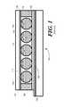
- FIG. 3illustrates a front, plan view of a conventional electrophoretic display.
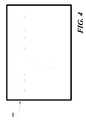
- FIG. 4illustrates a rear, plan view of an electrophoretic display having a transparent rear substrate.
- FIG. 5illustrates one embodiment of a front, plan view of an electrophoretic display having a first region and a second region, wherein pixels in the first region are larger than pixels in the second region, in accordance with embodiments of the invention.
- FIG. 6illustrates another embodiment of a front, plan view of an electrophoretic display having a first region and a second region, wherein pixels in the first region are larger than pixels in the second region.
- FIG. 7illustrates a schematic block diagram of one embodiment of an electrophoretic display having front, a first region and a second region, wherein pixels in the first region are larger than pixels in the second region.
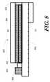
- FIG. 8illustrates a side, sectional view of a dual-sided electrophoretic display in accordance with embodiments of the invention.
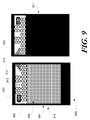
- FIG. 9illustrates a front and back view of one embodiment of an electrophoretic display in accordance with embodiments of the invention.
- FIG. 10illustrates a front and back view of one embodiment of an electrophoretic display in accordance with embodiments of the invention, where a shield covers one region.
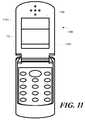
- FIGS. 11 and 12illustrate a portable electronic device having multiple displays employing an electrophoretic display in accordance with embodiments of the invention.
- FIG. 1illustrated therein is a sectional view of an electrophoretic display 100 .
- This conventional electrophoretic displayincludes a lamination adhesive 102 coupling a thin film transistor backplane 126 and a transparent front substrate 104 .
- An adhesive 106is generally employed to bond and seal the perimeters of the lamination adhesive 102 and the front substrate 104 , thereby forming a chamber 108 .
- the exemplary electrophoretic display of FIG. 1is one example of electrophoretic display technology useful for the discussion of embodiments of the invention herein, it will be clear to those of ordinary skill in the art having the benefit of this disclosure that the invention is not limited to this one type of display.
- Embodiments of the inventionare suitable for any display material operating by moving particles electrophoretically, including those using gels, powders, gasses, or other transfer media for the colored particles disposed therein.
- a plurality of capsules 110 , 112is disposed within in the chamber 108 .
- Each of the capsules 110 , 112encloses a medium 116 , such as hydrocarbon oil in liquid based electrophoretic materials, with light and dark particles 118 , 120 suspended therein.
- a medium 116such as hydrocarbon oil in liquid based electrophoretic materials
- Some of these particles 118which may be made from titanium dioxide, are generally white (i.e. reflective across the visible spectrum).
- Other particles 120may be pigmented with a dark colored dye so as to appear black. With surfactants and charging agents, the white particles 118 are positively charged while the black particles 120 are negatively charged.
- the front substrate 104is a transparent substrate that is tied electrically to ground or a common node by a layer of transparent electrode material 130 .
- the particles 118 , 120migrate electrophoretically so as to form an image viewable to the user. For example, when the white particles 118 move to the top of the capsule 110 they become visible as the color white to the user from the front side.
- the electric fieldpulls the black particles 120 to the bottom of the capsules 110 where they are hidden. By reversing this process, the black particles 120 appear at the top of the capsule 110 , which becomes visible as the color black.
- electrophoretic displaythat is visible from both sides. While conventional electrophoretic displays include only one transparent substrate, one solution to provide such a dual-sided display is to use two transparent substrates, one on each side of the display. A transparent electrode material, such as indium-tin oxide (In.sub.2 O.sub.3-SnO.sub.2) may then be used to render both sides of the display visible. There is, however, an inherent problem with this solution. The problem involves the aperture ratio that will be discussed in more detail below.
- FIG. 2illustrated therein is a rear, plan view of a pixel 200 in an electrophoretic display having a transparent rear substrate 201 and an indium-tin oxide electrode 202 disposed thereon.
- additional componentsinclude a thin film transistor 203 and a capacitor 204 .
- the capacitor 204stores a charge sufficient to induce the electric field along the electrode 201 , and the thin film transistor 203 regulates when the capacitor 204 charges and discharges.
- the thin film transistor 203 and the capacitor 204are not. They are generally manufactured from deposited metal and are thus opaque. As these components are disposed on the back substrate 201 , they effectively “block out” the color presented by the particles in the display. Thus, for a pixel with area x, using a capacitor and thin film transistor having an area y, only (x ⁇ y)/x of the pixel is viewable from the rear side of the display.
- the thin film transistor 203 and capacitor 204may block as much as 35-40% of the overall area of the pixel.
- the net resultis that a substantially reduced area of the pixel is viewable from the back side of the display.
- This substantially reduced arearesults in a view that looks fuzzy, grainy, non-existent, or illegible.
- the front view 300shown in FIG. 3
- the rear view 400shown in FIG. 4
- the blocking function of the thin film transistor 203 and capacitor 204effectively causes the contrast ratio—i.e. the ratio of the luminosity of the brightest and the darkest color on the display—of the rear view to be insufficiently large so as to be legible by a user.
- the present inventionresolves this problem in at least one region of the display such that that region of the display offers a contrast ratio of sufficient magnitude as to be viewable from both sides of the display.
- the display 500includes a first region 501 and a second region 502 . Both the first region 501 and the second region 502 include selectively operable elements or members, referred to herein as “pixels.”
- pixels 504 in the second region 502are larger than are pixels 503 in the first region 501 .
- a member size, i.e. a pixel, associated with the first region 501is at least two times smaller than a member size associated with the second region 502 .
- the pixels 504 in the second region 502are configured to be driven by thin film transistors and capacitors, indicated collectively with reference designator 506 , that have the same area as the thin film capacitors and transistors 505 of the first region 501 , the aperture ratio of the pixels 504 in the second region 502 is greater than the aperture ratio of the pixels 503 in the first region 501 .
- the aperture ratio of the pixels 504 in the second region 502is at least 80%.
- the increased aperture ratiotranslates into an overall contrast ratio in the second region 502 , when viewed from the rear, that is sufficiently legible along the back side of the display 500 .
- the first region 501may be referred to as a “high resolution” region, in that the pixels 503 are sufficiently small as to present easily viewable information to a user.
- the term “high resolution”is used herein to mean a display suitable for the presentation of text, information, and graphics with sufficient granularity as to be easily switched between graphics or text.
- the high-resolution regionwould be one suitable for presenting an image in the Joint Photographics Expert Group (JPG) format to the user.
- JPGJoint Photographics Expert Group
- One example of thiswould be a region having a 256 pixel by 128-pixel area.
- the second region 502may be referred to as a “low resolution” region because the pixels 504 are larger than those pixels 503 in the high-resolution region 501 .
- the low-resolution region 502comprises less selectively operable members—or pixels—per unit area than does the high-resolution region 501 .
- the low resolution region 502has sufficient granularity to present certain alphanumeric characters or icons to a user, by may not be suitable for presenting a photographic image.
- the low-resolution region 502includes pixels 504 that are at least twice as big as are the pixels 503 in the high-resolution region 501 .
- a pixel aperture ratio associated with pixels 504 in the low-resolution region 502is greater than a pixel aperture ratio associated with pixels 503 in the high-resolution region 501 .
- the pixels 504 in the low resolution region 502may be four, eight, sixteen, or more times larger than the pixels 503 in the low resolution region 502 .
- the pixels 504 in the low-resolution region 502are sufficiently large as to provide a contrast ratio—when viewed from the rear side of the display 500 —of at least two to one.
- the display 600 of FIG. 6includes a first region 601 and a second region 602 . Pixels 604 in the second region 602 are bigger than are pixels 603 in the first region 601 . In one embodiment, the pixels in the second region 602 are at least two times bigger than are pixels 603 in the first region 601 .
- the pixels 604 in the second region 602 of FIG. 6include at least some geometrically non-uniform members.
- the bars 605 in the signal strength indicator 606include bars of varying lengths that are non-geometrically uniform.
- the embodiment of FIG. 6includes pixels that are geometrically configured as specific shapes and symbols.
- the elements in group 607are configured as a character symbol.
- the operable members of group 607are configured as a seven-segment character.
- the operable members of group 608are configured as an icon element, with each operable member being configured as at least a portion of an icon element.
- the exemplary icon element shownis that of a battery indicator.
- Indicator 606is, as noted above, a signal strength indicator.
- FIG. 7illustrated therein is a schematic block diagram of a display 700 including a high-resolution region 701 and a low-resolution region 702 in accordance with one embodiment of the invention. From the schematic block diagram of FIG. 7 , the driver circuit 710 and various control lines may be seen.
- the display 700which is one element in a display assembly, is an electrophoretic display with the driver circuit 710 coupled thereto.
- the display 700includes a high-resolution region 701 and a low-resolution region 702 .
- Both the selectively operable members 703 of high-resolution region 701 and the selectively operable members 704 of the low-resolution region 702may be selectively actuated, in one embodiment, by a common driver circuit 710 .
- the driver circuit 710controls each selectively operable member by a plurality of gate lines 720 and source lines 721 running between the selectively operable members and the driver circuit 710 .
- the second region 702is visible from both a front side 730 and a rear side 731 of the electrophoretic display 700 .
- the selectively operable members 704 of the second region 702are sufficiently large that a contrast ratio associated with the second region 702 , as viewed from the rear side 731 , is greater than a contrast ratio associated with the first region 701 , as viewed from the rear side 731 .
- the contrast ratio of the first region 701when viewed from the rear side 731 , is less due to the presence of capacitors and thin film transistors 741 that block visibility of the selectively operable members 703 in the first region 701 .
- the capacitors and thin film resistors 741permit the driver circuit 710 to selectively operate each of the selectively operable members 703 in the first region.
- Each thin film transistoracts as a switch controlled by the driver circuit 710 to drive each of a corresponding selectively operable member.
- Each capacitorwhich is disposed proximately and coupled with its corresponding selectively operable member, provides drive energy to cause the particles in the display to move electrophoretically.
- capacitors and thin film resistors 741 in the second region 702permit the driver circuit 710 to selectively operate each of the selectively operable members 704 in the second region 702 .
- each of these capacitors and thin film transistors 741 , 742are disposed on the transparent substrate—i.e. a thin film transistor substrate—forming the back side of the display assembly.
- This substrateis sometimes referred to herein as the “thin film transistor backplane.”
- the selectively operable members 704 of the second region 702are larger in size than are the selectively operable members 703 of the first region 701 , there are fewer selectively operable members 704 in the second region 702 than are in the first region 701 .
- the second region 702further includes less thin film transistors and capacitors 742 per unit area than does the first region 701 .
- the size of the selectively operable members 704 in the second region 702is at least twice that of the selectively operable members 703 in the first region 701 . This means that a ratio of a visible surface area of each of the selectively operable members 704 in the second region 702 to a surface area of both the corresponding thin film transistor capacitor is at least two times greater in the second region 702 than in the first region 701 . This translates into a contrast ratio in the second region 702 that is sufficiently legible to a user.
- FIG. 8illustrated therein is a sectional side view of one embodiment of a dual sided electrophoretic display structure 800 in accordance with the invention.
- This exemplary display structure 800is suitable for use in an electronic device having display windows on opposite sides of a device housing.
- the display structure 800first includes an electrophoretic display film 801 , which is disposed between an optional light guide 802 and a thin film transistor backplane 803 .
- the thin film transistor backplane 803may be manufactured from any rigid, transparent material, but are preferably manufactured from rigid plastic or reinforced glass.
- the optional light guide 802is frequently manufactured from rigid plastic, but may also be constructed as a thin film assembly.
- the optional light guide 802acts to direct incident light to the electrophoretic film 801 and then back to the user's eye.
- a light guideis a substrate material that has refractive properties that direct light generally in a predetermined manner. Thus, when a ray of incident light passes through the optional light guide 802 , it may travel generally towards the display so as to be reflected back to the user's eye with little dispersion or refraction.
- the light guide 802is optional in that while it enhances performance, it is not required for the display 800 to function properly.
- the thin film transistor backplane 803is a hybrid or multifunction substrate, in that it both acts as an electrode layer for the particles in the electrophoretic film 801 and as a thin film transistor and/or capacitor substrate. Upon this thin film transistor backplane 803 are deposited the thin film transistors used by the driver circuit 710 to drive the various selectively operable members. The capacitors used to maintain a potential required for driving the particles in the electrophoretic film 801 . Further, the indium tin oxide electrodes used to apply the electric field to the particles in the electrophoretic film 801 may also be disposed on the thin film transistor backplane 803 .
- An optional moisture barrier layer 804may be optionally included between an outer substrate, e.g. substrate 802 , and the electrophoretic film 801 .
- This moisture barrier layer 804helps to prevent foreign moisture from damaging the electrochemical properties of the electrophoretic film 801 .
- the moisture barrier layer 804may also provide ultraviolet protection for the electrophoretic film 801 .
- the ends of the display structure 800may be sealed with adhesive 805 to form a sealed chamber.
- the thin film transistor backplane 803may be used to provide support for other elements as well.
- the driver circuit 806has been coupled to substrate 803 to form an integrated display assembly that includes both the display and the driver circuit 710 .
- mechanical supports, additional light guide sections, and alignment devices, e.g. light guide section 731may be disposed on the substrates to assist with integration or operation of the display structure 800 in an overall electronic device.
- FIG. 9illustrated therein is a front view 910 and a rear view 911 of one embodiment of a dual sided display 900 in accordance with one embodiment of the invention.
- the first region 901displays a matrix grid 950 by selective operation of the selectively operable members.
- the matrix grid 950is visible to a user on in the front view 910 .
- the matrix grid 950is not visible due to the aperture ratio of the selectively operable members in the first region 901 on the rear side of the display 900 .
- the non-translucent thin film transistors and capacitors used to drive each of the selectively operable memberscover a significant portion of each of the selectively operable members. This causes the aperture ratio of each to decrease. From the rear view 911 , this translates to a contrast ratio that is insufficient for a user to legible view the matrix grid 950 from the rear side.
- the second region 902it has been configured such that the larger selectively operable members present icons 912 , 913 , characters 914 , and symbols.
- the second region 902may include a battery status indicator 913 , a signal strength indicator 913 , seven segment alphanumeric characters 914 , and associated symbols 915 .
- each of these icons, symbols and charactersis legibly visible, as the contrast ratio in the second region is improved by the relative size of the selectively operable members compared to their corresponding thin film transistors and capacitors.
- each of the characters, icons, and symbolsare legible, although each is presented as a mirror image of that of the front view 910 .
- the second regionmay be configured such that a positive image is displayed when viewed from the rear view 911 .
- a reversed, mirror imagebecomes visible from the front view 910 . While some device designers may not mind this mirror image, others may.
- FIG. 10illustrated therein is one embodiment of a device assembly that eliminates the mirror image.
- an opaque shield 1001has been placed on the front side of the display 900 .
- the mirror image in the second region 902is not visible.
- the second region 902is visible.
- the shield 1001is disposed atop at least a portion of the second region 902 such that at least some of the second region 902 is not visible from the front view 910 .
- the display 900were used in a device having a first window through which the front view 910 were visible, at least a portion of the second region 902 would not be visible through the first window.
- FIGS. 11 and 12illustrated therein is such a device.
- the exemplary embodiment of FIGS. 11 and 12illustrates a portable electronic device 1100 that has a multi-windowed housing 1163 and employs a dual-sided electrophoretic display in accordance with embodiments of the invention.
- the dual-sided electrophoretic displayhas a first region 1101 that is visible through a first window 1161 .
- a second region 1102 of the dual-sided electrophoretic displayis visible through at least the first window 1161 and a second window 1162 .
- Each region 1101 , 1102includes selectively operable electrophoretic members that are selectively operable by a driver circuit.
- the driver circuitis common to both the members of the first region 1101 and the members of the second region 1102 .
- the windows 1161 , 1162are covered with substantially transparent lenses to keep out dust, dirt and debris.
- the multi-windowed housing 1163includes a movable portion, wherein the second window 1162 is visible when the multi-windowed housing 1163 is closed. When the multi-windowed housing 1163 is open, both the first window 1161 and the second window 1162 are visible, with the first window 1161 visible on the one side of the multi-windowed housing 1163 and the second window 1162 visible on the second side of the multi-windowed housing 1163 .
- the displayis shown in a movable flip housing portion in the illustrative embodiment of FIGS. 11 and 12 , it will be clear to those of ordinary skill in the art having the benefit of this disclosure that dual sided displays in accordance with embodiments of the invention could also be incorporated into a suitably thin electronic device having a one-piece housing.
- the contrast ratiowhen viewed from the second side of the electrophoretic display, is at least two to one.
- the contrast ratio, as viewed through the second window 1162is also at least two to one.
Landscapes
- Engineering & Computer Science (AREA)
- Physics & Mathematics (AREA)
- Computer Hardware Design (AREA)
- General Physics & Mathematics (AREA)
- Theoretical Computer Science (AREA)
- Electrochromic Elements, Electrophoresis, Or Variable Reflection Or Absorption Elements (AREA)
Abstract
Description
Claims (6)
Priority Applications (2)
| Application Number | Priority Date | Filing Date | Title |
|---|---|---|---|
| US11/741,877US8902152B2 (en) | 2007-04-30 | 2007-04-30 | Dual sided electrophoretic display |
| PCT/US2008/060960WO2008137290A1 (en) | 2007-04-30 | 2008-04-21 | Dual-sided electrophoretic display |
Applications Claiming Priority (1)
| Application Number | Priority Date | Filing Date | Title |
|---|---|---|---|
| US11/741,877US8902152B2 (en) | 2007-04-30 | 2007-04-30 | Dual sided electrophoretic display |
Publications (2)
| Publication Number | Publication Date |
|---|---|
| US20080266244A1 US20080266244A1 (en) | 2008-10-30 |
| US8902152B2true US8902152B2 (en) | 2014-12-02 |
Family
ID=39886358
Family Applications (1)
| Application Number | Title | Priority Date | Filing Date |
|---|---|---|---|
| US11/741,877Active2033-06-02US8902152B2 (en) | 2007-04-30 | 2007-04-30 | Dual sided electrophoretic display |
Country Status (2)
| Country | Link |
|---|---|
| US (1) | US8902152B2 (en) |
| WO (1) | WO2008137290A1 (en) |
Cited By (40)
| Publication number | Priority date | Publication date | Assignee | Title |
|---|---|---|---|---|
| US20160005721A1 (en)* | 2014-06-18 | 2016-01-07 | X-Celeprint Limited | Micro assembled led displays and lighting elements |
| US9716082B2 (en) | 2014-08-26 | 2017-07-25 | X-Celeprint Limited | Micro assembled hybrid displays and lighting elements |
| US9741785B2 (en) | 2014-09-25 | 2017-08-22 | X-Celeprint Limited | Display tile structure and tiled display |
| US9786646B2 (en) | 2015-12-23 | 2017-10-10 | X-Celeprint Limited | Matrix addressed device repair |
| US9818725B2 (en) | 2015-06-01 | 2017-11-14 | X-Celeprint Limited | Inorganic-light-emitter display with integrated black matrix |
| US9871345B2 (en) | 2015-06-09 | 2018-01-16 | X-Celeprint Limited | Crystalline color-conversion device |
| US9980341B2 (en) | 2016-09-22 | 2018-05-22 | X-Celeprint Limited | Multi-LED components |
| US9991163B2 (en) | 2014-09-25 | 2018-06-05 | X-Celeprint Limited | Small-aperture-ratio display with electrical component |
| US9997501B2 (en) | 2016-06-01 | 2018-06-12 | X-Celeprint Limited | Micro-transfer-printed light-emitting diode device |
| US9997102B2 (en) | 2016-04-19 | 2018-06-12 | X-Celeprint Limited | Wirelessly powered display and system |
| US9997100B2 (en) | 2014-09-25 | 2018-06-12 | X-Celeprint Limited | Self-compensating circuit for faulty display pixels |
| US10008483B2 (en) | 2016-04-05 | 2018-06-26 | X-Celeprint Limited | Micro-transfer printed LED and color filter structure |
| US10008465B2 (en) | 2011-06-08 | 2018-06-26 | X-Celeprint Limited | Methods for surface attachment of flipped active components |
| US10066819B2 (en) | 2015-12-09 | 2018-09-04 | X-Celeprint Limited | Micro-light-emitting diode backlight system |
| US10109753B2 (en) | 2016-02-19 | 2018-10-23 | X-Celeprint Limited | Compound micro-transfer-printed optical filter device |
| US10133426B2 (en) | 2015-06-18 | 2018-11-20 | X-Celeprint Limited | Display with micro-LED front light |
| US10150326B2 (en) | 2016-02-29 | 2018-12-11 | X-Celeprint Limited | Hybrid document with variable state |
| US10153256B2 (en) | 2016-03-03 | 2018-12-11 | X-Celeprint Limited | Micro-transfer printable electronic component |
| US10153257B2 (en) | 2016-03-03 | 2018-12-11 | X-Celeprint Limited | Micro-printed display |
| US10150325B2 (en) | 2016-02-29 | 2018-12-11 | X-Celeprint Limited | Hybrid banknote with electronic indicia |
| US10193025B2 (en) | 2016-02-29 | 2019-01-29 | X-Celeprint Limited | Inorganic LED pixel structure |
| US10199546B2 (en) | 2016-04-05 | 2019-02-05 | X-Celeprint Limited | Color-filter device |
| US10198890B2 (en) | 2016-04-19 | 2019-02-05 | X-Celeprint Limited | Hybrid banknote with electronic indicia using near-field-communications |
| US10200013B2 (en) | 2016-02-18 | 2019-02-05 | X-Celeprint Limited | Micro-transfer-printed acoustic wave filter device |
| US10217730B2 (en) | 2016-02-25 | 2019-02-26 | X-Celeprint Limited | Efficiently micro-transfer printing micro-scale devices onto large-format substrates |
| US10224231B2 (en) | 2016-11-15 | 2019-03-05 | X-Celeprint Limited | Micro-transfer-printable flip-chip structures and methods |
| US10230048B2 (en) | 2015-09-29 | 2019-03-12 | X-Celeprint Limited | OLEDs for micro transfer printing |
| US10255834B2 (en) | 2015-07-23 | 2019-04-09 | X-Celeprint Limited | Parallel redundant chiplet system for controlling display pixels |
| US10347168B2 (en) | 2016-11-10 | 2019-07-09 | X-Celeprint Limited | Spatially dithered high-resolution |
| US10361677B2 (en) | 2016-02-18 | 2019-07-23 | X-Celeprint Limited | Transverse bulk acoustic wave filter |
| US10380930B2 (en) | 2015-08-24 | 2019-08-13 | X-Celeprint Limited | Heterogeneous light emitter display system |
| US10396137B2 (en) | 2017-03-10 | 2019-08-27 | X-Celeprint Limited | Testing transfer-print micro-devices on wafer |
| US10395966B2 (en) | 2016-11-15 | 2019-08-27 | X-Celeprint Limited | Micro-transfer-printable flip-chip structures and methods |
| US10418331B2 (en) | 2010-11-23 | 2019-09-17 | X-Celeprint Limited | Interconnection structures and methods for transfer-printed integrated circuit elements with improved interconnection alignment tolerance |
| US10438859B2 (en) | 2016-12-19 | 2019-10-08 | X-Celeprint Limited | Transfer printed device repair |
| US10600671B2 (en) | 2016-11-15 | 2020-03-24 | X-Celeprint Limited | Micro-transfer-printable flip-chip structures and methods |
| US10782002B2 (en) | 2016-10-28 | 2020-09-22 | X Display Company Technology Limited | LED optical components |
| US11024608B2 (en) | 2017-03-28 | 2021-06-01 | X Display Company Technology Limited | Structures and methods for electrical connection of micro-devices and substrates |
| US11061276B2 (en) | 2015-06-18 | 2021-07-13 | X Display Company Technology Limited | Laser array display |
| US11137641B2 (en) | 2016-06-10 | 2021-10-05 | X Display Company Technology Limited | LED structure with polarized light emission |
Families Citing this family (11)
| Publication number | Priority date | Publication date | Assignee | Title |
|---|---|---|---|---|
| US7781784B2 (en)* | 2007-05-07 | 2010-08-24 | Samsung Electronics Co., Ltd. | Display apparatus with color pixels |
| US8059232B2 (en)* | 2008-02-08 | 2011-11-15 | Motorola Mobility, Inc. | Electronic device and LC shutter for polarization-sensitive switching between transparent and diffusive states |
| US7864270B2 (en)* | 2008-02-08 | 2011-01-04 | Motorola, Inc. | Electronic device and LC shutter with diffusive reflective polarizer |
| US20090213039A1 (en)* | 2008-02-21 | 2009-08-27 | Toppan Printing Co., Ltd. | Display device |
| JP5716294B2 (en)* | 2010-05-19 | 2015-05-13 | セイコーエプソン株式会社 | Display control method, display control apparatus, and program |
| US9087488B1 (en)* | 2011-09-15 | 2015-07-21 | Amazon Technologies, Inc. | Producing electro-optic display with seamless front surface |
| TWI467308B (en)* | 2012-03-16 | 2015-01-01 | E Ink Holdings Inc | Electrophoretic display apparatus |
| US9093050B1 (en)* | 2012-03-21 | 2015-07-28 | Amazon Technologies, Inc. | Determining when to delay sending updates to a display device |
| US10249247B2 (en)* | 2017-08-29 | 2019-04-02 | Shenzhen China Star Optoelectronics Semiconductor Display Technology Co., Ltd. | Transparent dual-sided display device and driving method thereof |
| US20200258478A1 (en)* | 2019-02-11 | 2020-08-13 | GM Global Technology Operations LLC | Programmable glass display |
| EP4238086A4 (en)* | 2020-11-02 | 2024-06-12 | E Ink Corporation | Methods for reducing image artifacts during partial updates of electrophoretic displays |
Citations (122)
| Publication number | Priority date | Publication date | Assignee | Title |
|---|---|---|---|---|
| US3915548A (en) | 1973-04-30 | 1975-10-28 | Hughes Aircraft Co | Holographic lens and liquid crystal image source for head-up display |
| US4017848A (en) | 1975-05-19 | 1977-04-12 | Rockwell International Corporation | Transparent keyboard switch and array |
| US4078257A (en) | 1976-08-23 | 1978-03-07 | Hewlett-Packard Company | Calculator apparatus with electronically alterable key symbols |
| US4422721A (en) | 1982-08-09 | 1983-12-27 | Optical Coating Laboratory, Inc. | Optical article having a conductive anti-reflection coating |
| US4462924A (en) | 1978-09-13 | 1984-07-31 | The Secretary Of State In Her Britannic Majesty's Government Of The United Kingdom Of Great Britain And Northern Ireland | Liquid crystal materials and devices |
| US4500173A (en) | 1983-05-02 | 1985-02-19 | Timex Corporation | Electroluminescent lamp for liquid crystal display |
| US4545648A (en) | 1980-10-30 | 1985-10-08 | Polaroid Corporation | Nacreous transflector illumination system for liquid crystal display |
| US4728936A (en) | 1986-04-11 | 1988-03-01 | Adt, Inc. | Control and display system |
| US4893903A (en) | 1985-05-06 | 1990-01-16 | Taliq Corporation | Flashing advisory sign |
| JPH03180920A (en) | 1989-12-08 | 1991-08-06 | Fujitsu Ltd | Keyboard device |
| US5121234A (en) | 1990-10-29 | 1992-06-09 | Honeywell Incorporated | Dichroic liquid crystal display with integral electroluminescent backlighting |
| US5225818A (en) | 1990-11-26 | 1993-07-06 | Data Entry Products, Incorporated | Data entry control panel |
| US5231381A (en) | 1989-10-02 | 1993-07-27 | U.S. Philips Corp. | Data processing system with a touch screen and a digitizing tablet, both integrated in an input device |
| US5376948A (en) | 1992-03-25 | 1994-12-27 | Visage, Inc. | Method of and apparatus for touch-input computer and related display employing touch force location external to the display |
| JPH0863271A (en) | 1994-08-19 | 1996-03-08 | Fujitsu General Ltd | keyboard |
| US5600459A (en) | 1993-12-20 | 1997-02-04 | Roy; Howard S. | Multiple-shutter flat-panel display having individually controlled pixels and method for making same |
| KR19980026397A (en) | 1996-10-09 | 1998-07-15 | 김영수 | Optional character display on the keyboard |
| US5796454A (en) | 1996-12-04 | 1998-08-18 | Advanced Display Systems, Inc. | Cholesteric liquid crystal display employing circular polarizer and methods of operation and manufacture therefor |
| US5818615A (en) | 1993-12-02 | 1998-10-06 | Ois Optical Imaging Systems, Inc. | Liquid crystal display with patterned retardation films |
| US6047196A (en) | 1995-11-24 | 2000-04-04 | Nokia Mobile Phones, Ltd. | Communication device with two modes of operation |
| US6058164A (en) | 1995-03-01 | 2000-05-02 | Fujitsu Limited | Mode-switchable telephone and mode setting and switching methods for the same |
| US6103384A (en) | 1998-07-01 | 2000-08-15 | Mario; Spinelli | Process for the superficial decoration of objects made of transparent vitreous material |
| US6144359A (en) | 1998-03-30 | 2000-11-07 | Rockwell Science Center | Liquid crystal displays utilizing polymer dispersed liquid crystal devices for enhanced performance and reduced power |
| US6150962A (en) | 1995-12-11 | 2000-11-21 | Phone.Com, Inc. | Predictive data entry method for a keyboard |
| US6188379B1 (en) | 1996-11-05 | 2001-02-13 | Citizen Watch Co., Ltd. | Color display system and method of driving the same |
| WO2001013209A1 (en) | 1999-08-18 | 2001-02-22 | Ericsson, Inc. | Electronic devices including keypads that illuminate in response to proximity of a user and methods of operating such electronic devices |
| US6211931B1 (en) | 1998-01-27 | 2001-04-03 | Hitachi Maxell, Ltd. | Polymer-dispersed liquid crystal composition and liquid crystal display elements using the composition |
| KR200225646Y1 (en) | 2000-12-21 | 2001-06-01 | 엘지전자주식회사 | Ring signal informing apparatus for Cellular phone |
| US6243080B1 (en) | 1998-07-14 | 2001-06-05 | Ericsson Inc. | Touch-sensitive panel with selector |
| US6271835B1 (en) | 1998-09-03 | 2001-08-07 | Nortel Networks Limited | Touch-screen input device |
| GB2359178A (en) | 1999-11-13 | 2001-08-15 | British Ind Graphics Ltd | Improvements in and relating to display units |
| GB2348039B (en) | 1999-03-17 | 2001-09-26 | Motorola Inc | Display with aligned optical shutter and backlight cells applicable for use with a touchscreen |
| US6310609B1 (en) | 1997-04-17 | 2001-10-30 | Nokia Mobile Phones Limited | User interface with guide lights |
| US6327376B1 (en) | 1997-12-04 | 2001-12-04 | U.S. Philips Corporation | Electronic apparatus comprising fingerprint sensing devices |
| JP2002049461A (en) | 2000-08-04 | 2002-02-15 | Toppan Printing Co Ltd | Data input device |
| WO2002031807A1 (en) | 2000-10-10 | 2002-04-18 | Motorola Inc., A Corporation Of The State Of Delaware | Data entry device |
| US20020090980A1 (en) | 2000-12-05 | 2002-07-11 | Wilcox Russell J. | Displays for portable electronic apparatus |
| US6470196B1 (en) | 1998-10-09 | 2002-10-22 | Nec Corporation | Portable communication apparatus |
| US20030020999A1 (en) | 2001-04-04 | 2003-01-30 | International Business Machines Corporation | Electronic apparatus and electronic apparatus information display method |
| US20030025679A1 (en) | 1999-06-22 | 2003-02-06 | Cirque Corporation | System for disposing a proximity sensitive touchpad behind a mobile phone keypad |
| US20030054867A1 (en) | 2001-09-18 | 2003-03-20 | Homayoun Dowlat | Method and apparatus for alerting users of incoming calls and messages |
| US20030058223A1 (en) | 2001-09-21 | 2003-03-27 | Tracy James L. | Adaptable keypad and button mechanism therefor |
| JP2003101622A (en) | 2001-07-25 | 2003-04-04 | Hewlett Packard Co <Hp> | Communication device and method |
| US6574487B1 (en) | 2000-02-23 | 2003-06-03 | Motorola, Inc. | Communication device with a dual-sided liquid crystal display |
| US6574044B1 (en) | 1999-10-25 | 2003-06-03 | 3M Innovative Properties Company | Polarizer constructions and display devices exhibiting unique color effects |
| US20030161093A1 (en) | 1999-05-14 | 2003-08-28 | Lawrence Lam | Display housing for computing device |
| EP1341029A2 (en) | 2002-03-01 | 2003-09-03 | Fossil, Inc. | Improved time piece |
| US6646697B1 (en) | 1997-07-18 | 2003-11-11 | Citizen Watch Co., Ltd. | Liquid crystal display |
| US6662244B1 (en) | 1999-07-30 | 2003-12-09 | Sony Corporation | Information terminal |
| WO2003104884A2 (en) | 2002-06-10 | 2003-12-18 | E Ink Corporation | Components and methods for electro-optic displays |
| US20040036680A1 (en) | 2002-08-26 | 2004-02-26 | Mark Davis | User-interface features for computers with contact-sensitive displays |
| KR20040019677A (en) | 2002-08-29 | 2004-03-06 | 엘지전자 주식회사 | Apparatus for visualizing call on a telephone |
| US6704004B1 (en) | 2000-08-17 | 2004-03-09 | Nokia Mobile Phones Ltd. | Arrangement for integration of key illumination into keymat of portable electronic devices |
| US20040058718A1 (en) | 2002-09-19 | 2004-03-25 | Samsung Electronics Co., Ltd. | Method for giving notice of an incoming call in a mobile communication terminal |
| US20040092196A1 (en) | 2000-06-06 | 2004-05-13 | Peter Van De Witte | Liquid crystal display device |
| US20040104826A1 (en) | 2002-10-31 | 2004-06-03 | Harald Philipp | Charge transfer capacitive position sensor |
| US6768481B2 (en) | 1997-07-25 | 2004-07-27 | Seiko Epson Corporation | Display device and electronic equipment employing the same |
| US20040189591A1 (en) | 2003-03-27 | 2004-09-30 | Breuil Thomas L. Du | Method and apparatus for a programmable electrophoretic remote control |
| EP1467536B1 (en) | 2003-05-08 | 2004-10-20 | Siemens Aktiengesellschaft | Device for state-dependently adjusting the appearance of the cover of a portable electronic device, and cover therefore |
| US20040218121A1 (en) | 2003-05-01 | 2004-11-04 | Zhiming Zhuang | Transflective color liquid crystal display with internal rear polarizer |
| US6813957B1 (en) | 1999-11-26 | 2004-11-09 | Karl-Otto Platz | Capacitive sensor on a transparent carrier |
| US6819380B2 (en) | 2002-10-11 | 2004-11-16 | Toppoly Optoelectronics Corp. | Double-sided LCD panel |
| US6819316B2 (en) | 2001-04-17 | 2004-11-16 | 3M Innovative Properties Company | Flexible capacitive touch sensor |
| US20040265602A1 (en) | 2001-10-05 | 2004-12-30 | Taichi Kobayashi | Transparent electroconductive film, method for manufacture thereof, and touch panel |
| US20050007339A1 (en) | 2003-06-12 | 2005-01-13 | Tadamitsu Sato | Inputting method and input device |
| US20050020316A1 (en) | 2003-07-25 | 2005-01-27 | Hassan Mahini | Event list menu for accessing menu items in a hierarchical menu |
| US20050020325A1 (en) | 2003-07-24 | 2005-01-27 | Motorola, Inc. | Multi-configuration portable electronic device and method for operating the same |
| US20050030048A1 (en) | 2003-08-05 | 2005-02-10 | Bolender Robert J. | Capacitive sensing device for use in a keypad assembly |
| US20050030292A1 (en) | 2001-12-12 | 2005-02-10 | Diederiks Elmo Marcus Attila | Display system with tactile guidance |
| US6864945B2 (en) | 2000-08-30 | 2005-03-08 | Sharp Kabushiki Kaisha | Liquid crystal display and manufacturing method thereof |
| US20050064913A1 (en) | 2003-08-18 | 2005-03-24 | Kim Byung-Jin | Incoming call alerting method and mobile communication terminal using the same |
| JP2005100186A (en) | 2003-09-25 | 2005-04-14 | Casio Comput Co Ltd | Software keyboard display device and display program |
| US20050088417A1 (en) | 2003-10-24 | 2005-04-28 | Mulligan Roger C. | Tactile touch-sensing system |
| US20050093767A1 (en)* | 2003-10-30 | 2005-05-05 | Ritdisplay Corporation | Dual display device |
| US20050114825A1 (en) | 2003-11-24 | 2005-05-26 | International Business Machines Corporation | Laptop computer including a touch-sensitive display and method of driving the laptop computer |
| US20050134549A1 (en)* | 2003-09-18 | 2005-06-23 | Citizen Watch Co.,Ltd. | Display Apparatus |
| US6914874B2 (en) | 1998-03-10 | 2005-07-05 | Jvc Victor Company Of Japan, Ltd. | Disklike recording media, a method for detecting forged disks, an anti-forgery system for performing a true-false judgement based on information collected from the recording media, and a manufacturing apparatus for recording information in the disks |
| US20050243069A1 (en) | 2004-04-30 | 2005-11-03 | Rudy Yorio | Display-input apparatus for a multi-configuration portable device |
| US6968744B1 (en) | 2004-10-18 | 2005-11-29 | Silverbrook Research Pty Ltd | Capacitative pressure sensor with close electrodes |
| US20050266891A1 (en) | 2003-03-14 | 2005-12-01 | Mullen Jeffrey D | Systems and methods for providing remote incoming call notification for cellular phones |
| US20050264190A1 (en) | 2004-05-28 | 2005-12-01 | Park Young-Jong | Double-sided organic electroluminescent display having optical shutter and information terminal using the same |
| JP2005352987A (en) | 2004-06-14 | 2005-12-22 | Mitsubishi Electric Corp | Key input device |
| US20060026535A1 (en) | 2004-07-30 | 2006-02-02 | Apple Computer Inc. | Mode-based graphical user interfaces for touch sensitive input devices |
| US20060038937A1 (en) | 2004-08-12 | 2006-02-23 | Seiko Epson Corporation | Electro-optical device, method of manufacturing the same, and electronic apparatus |
| US20060046792A1 (en) | 2004-08-31 | 2006-03-02 | Hassemer Brian J | Hinge apparatus and methods therefor |
| JP2006091486A (en) | 2004-09-24 | 2006-04-06 | Seiko Epson Corp | Electro-optical device and electronic apparatus |
| US20060146012A1 (en) | 2005-01-04 | 2006-07-06 | Arneson Theodore R | System and method for automatic display switching |
| US20060161870A1 (en) | 2004-07-30 | 2006-07-20 | Apple Computer, Inc. | Proximity detector in handheld device |
| US20060161871A1 (en) | 2004-07-30 | 2006-07-20 | Apple Computer, Inc. | Proximity detector in handheld device |
| US20060166702A1 (en) | 2005-01-24 | 2006-07-27 | Dietz Paul H | Cellular telephone with ear proximity display and lighting control |
| US20060197753A1 (en) | 2005-03-04 | 2006-09-07 | Hotelling Steven P | Multi-functional hand-held device |
| US7106517B2 (en) | 2003-12-31 | 2006-09-12 | General Electric Company | Display optical films |
| JP2006243658A (en) | 2005-03-07 | 2006-09-14 | Sharp Corp | Panel substrate, method for manufacturing panel substrate, and method for manufacturing liquid crystal display panel |
| US7123945B2 (en)* | 2001-11-26 | 2006-10-17 | Sony Corporation | Task display switching method, portable apparatus and portable communications apparatus |
| US7127705B2 (en) | 2000-09-06 | 2006-10-24 | Oracle International Corporation | Developing applications online |
| WO2006116145A2 (en) | 2005-04-22 | 2006-11-02 | Microsoft Corporation | Auto-suggest lists and handwritten input |
| US7139114B2 (en) | 2004-12-20 | 2006-11-21 | Xerox Corporation | Bisymmetrical electric paper and a system therefor |
| WO2006123294A2 (en) | 2005-05-19 | 2006-11-23 | Koninklijke Philips Electronics, N.V. | Apparatus and method to enhance navigation in a user interface for mobile devices |
| US20060266640A1 (en) | 2005-05-26 | 2006-11-30 | Halsey Eugene L Iv | Capacitive touch screen and method of making same |
| KR100652767B1 (en) | 2005-11-11 | 2006-12-04 | 엘지전자 주식회사 | Screen display device and method of mobile communication terminal |
| US20060277472A1 (en) | 2005-06-07 | 2006-12-07 | Sony Computer Entertainment Inc. | Screen display program, computer readable recording medium recorded with screen display program, screen display apparatus, portable terminal apparatus, and screen display method |
| WO2006094308A3 (en) | 2005-03-04 | 2006-12-14 | Apple Computer | Multi-functional hand-held device |
| US20060290871A1 (en) | 2005-06-22 | 2006-12-28 | Sanyo Epson Imaging Devices Corp. | Electro-optical device, method of manufacturing the same, and electronic apparatus |
| KR20060134659A (en) | 2005-06-23 | 2006-12-28 | 엘지.필립스 엘시디 주식회사 | Display device and manufacturing method |
| US20070030438A1 (en) | 2005-07-20 | 2007-02-08 | Min-Feng Chiang | Arrangement of photo spacer material |
| US7180672B2 (en) | 2002-05-20 | 2007-02-20 | General Electric Company | Optical substrate and method of making |
| US20070052689A1 (en) | 2005-09-02 | 2007-03-08 | Lg Electronics Inc. | Mobile communication terminal having content data scrolling capability and method for scrolling through content data |
| US20070075965A1 (en) | 2005-09-30 | 2007-04-05 | Brian Huppi | Automated response to and sensing of user activity in portable devices |
| US20070097595A1 (en) | 2005-09-08 | 2007-05-03 | Nokia Corporation | Multipurpose programmable adjustable keyboard (MPAK) |
| WO2007063809A1 (en) | 2005-11-29 | 2007-06-07 | Fujifilm Corporation | Substrate for liquid crystal display device, liquid crystal display element, and liquid crystal display device |
| US20070152983A1 (en) | 2005-12-30 | 2007-07-05 | Apple Computer, Inc. | Touch pad with symbols based on mode |
| US20070164986A1 (en) | 2006-01-16 | 2007-07-19 | Samsung Electronics Co., Ltd. | Interface apparatus and method using electronic paper |
| KR20070109603A (en) | 2006-05-12 | 2007-11-15 | 엘지.필립스 엘시디 주식회사 | Electrophoretic display device and manufacturing method |
| US20070273662A1 (en) | 2006-05-26 | 2007-11-29 | Hon Hai Precision Industry Co., Ltd. | Display apparatus and display method for a portable device |
| US7345671B2 (en) | 2001-10-22 | 2008-03-18 | Apple Inc. | Method and apparatus for use of rotational user inputs |
| US20080122796A1 (en) | 2006-09-06 | 2008-05-29 | Jobs Steven P | Touch Screen Device, Method, and Graphical User Interface for Determining Commands by Applying Heuristics |
| US20080169944A1 (en) | 2007-01-15 | 2008-07-17 | Cisco Technology, Inc. | Dynamic Number Keypad for Networked Phones |
| US20080204417A1 (en) | 2007-02-27 | 2008-08-28 | Pierce Paul M | Multimodal Adaptive User Interface for a Portable Electronic Device |
| US20080204463A1 (en) | 2007-02-27 | 2008-08-28 | Adam Cybart | Adaptable User Interface and Mechanism for a Title Portable Electronic Device |
| US20080211734A1 (en) | 2005-06-14 | 2008-09-04 | Koninklijke Philips Electronics, N.V. | Combined Single/Multiple View-Display |
| US20080309589A1 (en) | 2007-06-13 | 2008-12-18 | Morales Joseph M | Segmented Electroluminescent Device for Morphing User Interface |
| US20080316397A1 (en) | 2007-06-22 | 2008-12-25 | Polak Robert D | Colored Morphing Apparatus for an Electronic Device |
Family Cites Families (1)
| Publication number | Priority date | Publication date | Assignee | Title |
|---|---|---|---|---|
| US20080021173A1 (en)* | 2004-06-25 | 2008-01-24 | Masataka Nakanishi | Epoxy Resin, Epoxy Resin Composition And Cured Product Thereof |
- 2007
- 2007-04-30USUS11/741,877patent/US8902152B2/enactiveActive
- 2008
- 2008-04-21WOPCT/US2008/060960patent/WO2008137290A1/enactiveApplication Filing
Patent Citations (125)
| Publication number | Priority date | Publication date | Assignee | Title |
|---|---|---|---|---|
| US3915548A (en) | 1973-04-30 | 1975-10-28 | Hughes Aircraft Co | Holographic lens and liquid crystal image source for head-up display |
| US4017848A (en) | 1975-05-19 | 1977-04-12 | Rockwell International Corporation | Transparent keyboard switch and array |
| US4078257A (en) | 1976-08-23 | 1978-03-07 | Hewlett-Packard Company | Calculator apparatus with electronically alterable key symbols |
| US4462924A (en) | 1978-09-13 | 1984-07-31 | The Secretary Of State In Her Britannic Majesty's Government Of The United Kingdom Of Great Britain And Northern Ireland | Liquid crystal materials and devices |
| US4545648A (en) | 1980-10-30 | 1985-10-08 | Polaroid Corporation | Nacreous transflector illumination system for liquid crystal display |
| US4422721A (en) | 1982-08-09 | 1983-12-27 | Optical Coating Laboratory, Inc. | Optical article having a conductive anti-reflection coating |
| US4500173A (en) | 1983-05-02 | 1985-02-19 | Timex Corporation | Electroluminescent lamp for liquid crystal display |
| US4893903A (en) | 1985-05-06 | 1990-01-16 | Taliq Corporation | Flashing advisory sign |
| US4728936A (en) | 1986-04-11 | 1988-03-01 | Adt, Inc. | Control and display system |
| US5231381A (en) | 1989-10-02 | 1993-07-27 | U.S. Philips Corp. | Data processing system with a touch screen and a digitizing tablet, both integrated in an input device |
| JPH03180920A (en) | 1989-12-08 | 1991-08-06 | Fujitsu Ltd | Keyboard device |
| US5121234A (en) | 1990-10-29 | 1992-06-09 | Honeywell Incorporated | Dichroic liquid crystal display with integral electroluminescent backlighting |
| US5225818A (en) | 1990-11-26 | 1993-07-06 | Data Entry Products, Incorporated | Data entry control panel |
| US5376948A (en) | 1992-03-25 | 1994-12-27 | Visage, Inc. | Method of and apparatus for touch-input computer and related display employing touch force location external to the display |
| US5818615A (en) | 1993-12-02 | 1998-10-06 | Ois Optical Imaging Systems, Inc. | Liquid crystal display with patterned retardation films |
| US5600459A (en) | 1993-12-20 | 1997-02-04 | Roy; Howard S. | Multiple-shutter flat-panel display having individually controlled pixels and method for making same |
| JPH0863271A (en) | 1994-08-19 | 1996-03-08 | Fujitsu General Ltd | keyboard |
| US6058164A (en) | 1995-03-01 | 2000-05-02 | Fujitsu Limited | Mode-switchable telephone and mode setting and switching methods for the same |
| US6047196A (en) | 1995-11-24 | 2000-04-04 | Nokia Mobile Phones, Ltd. | Communication device with two modes of operation |
| US6150962A (en) | 1995-12-11 | 2000-11-21 | Phone.Com, Inc. | Predictive data entry method for a keyboard |
| KR19980026397A (en) | 1996-10-09 | 1998-07-15 | 김영수 | Optional character display on the keyboard |
| US6188379B1 (en) | 1996-11-05 | 2001-02-13 | Citizen Watch Co., Ltd. | Color display system and method of driving the same |
| US5796454A (en) | 1996-12-04 | 1998-08-18 | Advanced Display Systems, Inc. | Cholesteric liquid crystal display employing circular polarizer and methods of operation and manufacture therefor |
| US6310609B1 (en) | 1997-04-17 | 2001-10-30 | Nokia Mobile Phones Limited | User interface with guide lights |
| US6646697B1 (en) | 1997-07-18 | 2003-11-11 | Citizen Watch Co., Ltd. | Liquid crystal display |
| US6768481B2 (en) | 1997-07-25 | 2004-07-27 | Seiko Epson Corporation | Display device and electronic equipment employing the same |
| US6327376B1 (en) | 1997-12-04 | 2001-12-04 | U.S. Philips Corporation | Electronic apparatus comprising fingerprint sensing devices |
| US6211931B1 (en) | 1998-01-27 | 2001-04-03 | Hitachi Maxell, Ltd. | Polymer-dispersed liquid crystal composition and liquid crystal display elements using the composition |
| US6914874B2 (en) | 1998-03-10 | 2005-07-05 | Jvc Victor Company Of Japan, Ltd. | Disklike recording media, a method for detecting forged disks, an anti-forgery system for performing a true-false judgement based on information collected from the recording media, and a manufacturing apparatus for recording information in the disks |
| US6144359A (en) | 1998-03-30 | 2000-11-07 | Rockwell Science Center | Liquid crystal displays utilizing polymer dispersed liquid crystal devices for enhanced performance and reduced power |
| US6103384A (en) | 1998-07-01 | 2000-08-15 | Mario; Spinelli | Process for the superficial decoration of objects made of transparent vitreous material |
| US6243080B1 (en) | 1998-07-14 | 2001-06-05 | Ericsson Inc. | Touch-sensitive panel with selector |
| US6271835B1 (en) | 1998-09-03 | 2001-08-07 | Nortel Networks Limited | Touch-screen input device |
| US6470196B1 (en) | 1998-10-09 | 2002-10-22 | Nec Corporation | Portable communication apparatus |
| GB2348039B (en) | 1999-03-17 | 2001-09-26 | Motorola Inc | Display with aligned optical shutter and backlight cells applicable for use with a touchscreen |
| US6842170B1 (en) | 1999-03-17 | 2005-01-11 | Motorola, Inc. | Display with aligned optical shutter and backlight cells applicable for use with a touchscreen |
| US20030161093A1 (en) | 1999-05-14 | 2003-08-28 | Lawrence Lam | Display housing for computing device |
| US20030025679A1 (en) | 1999-06-22 | 2003-02-06 | Cirque Corporation | System for disposing a proximity sensitive touchpad behind a mobile phone keypad |
| US6662244B1 (en) | 1999-07-30 | 2003-12-09 | Sony Corporation | Information terminal |
| WO2001013209A1 (en) | 1999-08-18 | 2001-02-22 | Ericsson, Inc. | Electronic devices including keypads that illuminate in response to proximity of a user and methods of operating such electronic devices |
| US6768586B2 (en) | 1999-10-25 | 2004-07-27 | 3M Innovative Properties Company | Polarizer constructions and display devices exhibiting unique color effects |
| US20040246580A1 (en) | 1999-10-25 | 2004-12-09 | 3M Innovative Properties Company | Polarizer constructions and display devices exhibiting unique color effects |
| US6574044B1 (en) | 1999-10-25 | 2003-06-03 | 3M Innovative Properties Company | Polarizer constructions and display devices exhibiting unique color effects |
| GB2359178A (en) | 1999-11-13 | 2001-08-15 | British Ind Graphics Ltd | Improvements in and relating to display units |
| US6813957B1 (en) | 1999-11-26 | 2004-11-09 | Karl-Otto Platz | Capacitive sensor on a transparent carrier |
| US6574487B1 (en) | 2000-02-23 | 2003-06-03 | Motorola, Inc. | Communication device with a dual-sided liquid crystal display |
| US20040092196A1 (en) | 2000-06-06 | 2004-05-13 | Peter Van De Witte | Liquid crystal display device |
| JP2002049461A (en) | 2000-08-04 | 2002-02-15 | Toppan Printing Co Ltd | Data input device |
| US6704004B1 (en) | 2000-08-17 | 2004-03-09 | Nokia Mobile Phones Ltd. | Arrangement for integration of key illumination into keymat of portable electronic devices |
| US6864945B2 (en) | 2000-08-30 | 2005-03-08 | Sharp Kabushiki Kaisha | Liquid crystal display and manufacturing method thereof |
| US7127705B2 (en) | 2000-09-06 | 2006-10-24 | Oracle International Corporation | Developing applications online |
| WO2002031807A1 (en) | 2000-10-10 | 2002-04-18 | Motorola Inc., A Corporation Of The State Of Delaware | Data entry device |
| US20020090980A1 (en) | 2000-12-05 | 2002-07-11 | Wilcox Russell J. | Displays for portable electronic apparatus |
| KR200225646Y1 (en) | 2000-12-21 | 2001-06-01 | 엘지전자주식회사 | Ring signal informing apparatus for Cellular phone |
| US20030020999A1 (en) | 2001-04-04 | 2003-01-30 | International Business Machines Corporation | Electronic apparatus and electronic apparatus information display method |
| US6819316B2 (en) | 2001-04-17 | 2004-11-16 | 3M Innovative Properties Company | Flexible capacitive touch sensor |
| JP2003101622A (en) | 2001-07-25 | 2003-04-04 | Hewlett Packard Co <Hp> | Communication device and method |
| US20030054867A1 (en) | 2001-09-18 | 2003-03-20 | Homayoun Dowlat | Method and apparatus for alerting users of incoming calls and messages |
| US20030058223A1 (en) | 2001-09-21 | 2003-03-27 | Tracy James L. | Adaptable keypad and button mechanism therefor |
| US20040265602A1 (en) | 2001-10-05 | 2004-12-30 | Taichi Kobayashi | Transparent electroconductive film, method for manufacture thereof, and touch panel |
| US7345671B2 (en) | 2001-10-22 | 2008-03-18 | Apple Inc. | Method and apparatus for use of rotational user inputs |
| US7123945B2 (en)* | 2001-11-26 | 2006-10-17 | Sony Corporation | Task display switching method, portable apparatus and portable communications apparatus |
| US20050030292A1 (en) | 2001-12-12 | 2005-02-10 | Diederiks Elmo Marcus Attila | Display system with tactile guidance |
| EP1341029A2 (en) | 2002-03-01 | 2003-09-03 | Fossil, Inc. | Improved time piece |
| US7180672B2 (en) | 2002-05-20 | 2007-02-20 | General Electric Company | Optical substrate and method of making |
| WO2003104884A2 (en) | 2002-06-10 | 2003-12-18 | E Ink Corporation | Components and methods for electro-optic displays |
| US20040036680A1 (en) | 2002-08-26 | 2004-02-26 | Mark Davis | User-interface features for computers with contact-sensitive displays |
| KR20040019677A (en) | 2002-08-29 | 2004-03-06 | 엘지전자 주식회사 | Apparatus for visualizing call on a telephone |
| US20040058718A1 (en) | 2002-09-19 | 2004-03-25 | Samsung Electronics Co., Ltd. | Method for giving notice of an incoming call in a mobile communication terminal |
| US6819380B2 (en) | 2002-10-11 | 2004-11-16 | Toppoly Optoelectronics Corp. | Double-sided LCD panel |
| US20040104826A1 (en) | 2002-10-31 | 2004-06-03 | Harald Philipp | Charge transfer capacitive position sensor |
| US20050266891A1 (en) | 2003-03-14 | 2005-12-01 | Mullen Jeffrey D | Systems and methods for providing remote incoming call notification for cellular phones |
| US20040189591A1 (en) | 2003-03-27 | 2004-09-30 | Breuil Thomas L. Du | Method and apparatus for a programmable electrophoretic remote control |
| US20040218121A1 (en) | 2003-05-01 | 2004-11-04 | Zhiming Zhuang | Transflective color liquid crystal display with internal rear polarizer |
| EP1467536B1 (en) | 2003-05-08 | 2004-10-20 | Siemens Aktiengesellschaft | Device for state-dependently adjusting the appearance of the cover of a portable electronic device, and cover therefore |
| US20050007339A1 (en) | 2003-06-12 | 2005-01-13 | Tadamitsu Sato | Inputting method and input device |
| US20050020325A1 (en) | 2003-07-24 | 2005-01-27 | Motorola, Inc. | Multi-configuration portable electronic device and method for operating the same |
| US20050020316A1 (en) | 2003-07-25 | 2005-01-27 | Hassan Mahini | Event list menu for accessing menu items in a hierarchical menu |
| US20050030048A1 (en) | 2003-08-05 | 2005-02-10 | Bolender Robert J. | Capacitive sensing device for use in a keypad assembly |
| US20050064913A1 (en) | 2003-08-18 | 2005-03-24 | Kim Byung-Jin | Incoming call alerting method and mobile communication terminal using the same |
| US20050134549A1 (en)* | 2003-09-18 | 2005-06-23 | Citizen Watch Co.,Ltd. | Display Apparatus |
| JP2005100186A (en) | 2003-09-25 | 2005-04-14 | Casio Comput Co Ltd | Software keyboard display device and display program |
| US20050088417A1 (en) | 2003-10-24 | 2005-04-28 | Mulligan Roger C. | Tactile touch-sensing system |
| US20050093767A1 (en)* | 2003-10-30 | 2005-05-05 | Ritdisplay Corporation | Dual display device |
| US20050114825A1 (en) | 2003-11-24 | 2005-05-26 | International Business Machines Corporation | Laptop computer including a touch-sensitive display and method of driving the laptop computer |
| US7106517B2 (en) | 2003-12-31 | 2006-09-12 | General Electric Company | Display optical films |
| US20050243069A1 (en) | 2004-04-30 | 2005-11-03 | Rudy Yorio | Display-input apparatus for a multi-configuration portable device |
| US20050264190A1 (en) | 2004-05-28 | 2005-12-01 | Park Young-Jong | Double-sided organic electroluminescent display having optical shutter and information terminal using the same |
| JP2005352987A (en) | 2004-06-14 | 2005-12-22 | Mitsubishi Electric Corp | Key input device |
| US20060161871A1 (en) | 2004-07-30 | 2006-07-20 | Apple Computer, Inc. | Proximity detector in handheld device |
| US20060026535A1 (en) | 2004-07-30 | 2006-02-02 | Apple Computer Inc. | Mode-based graphical user interfaces for touch sensitive input devices |
| US20060161870A1 (en) | 2004-07-30 | 2006-07-20 | Apple Computer, Inc. | Proximity detector in handheld device |
| US20060038937A1 (en) | 2004-08-12 | 2006-02-23 | Seiko Epson Corporation | Electro-optical device, method of manufacturing the same, and electronic apparatus |
| US20060046792A1 (en) | 2004-08-31 | 2006-03-02 | Hassemer Brian J | Hinge apparatus and methods therefor |
| JP2006091486A (en) | 2004-09-24 | 2006-04-06 | Seiko Epson Corp | Electro-optical device and electronic apparatus |
| US6968744B1 (en) | 2004-10-18 | 2005-11-29 | Silverbrook Research Pty Ltd | Capacitative pressure sensor with close electrodes |
| US7139114B2 (en) | 2004-12-20 | 2006-11-21 | Xerox Corporation | Bisymmetrical electric paper and a system therefor |
| US20060146012A1 (en) | 2005-01-04 | 2006-07-06 | Arneson Theodore R | System and method for automatic display switching |
| US20060166702A1 (en) | 2005-01-24 | 2006-07-27 | Dietz Paul H | Cellular telephone with ear proximity display and lighting control |
| WO2006094308A3 (en) | 2005-03-04 | 2006-12-14 | Apple Computer | Multi-functional hand-held device |
| US20060197753A1 (en) | 2005-03-04 | 2006-09-07 | Hotelling Steven P | Multi-functional hand-held device |
| JP2006243658A (en) | 2005-03-07 | 2006-09-14 | Sharp Corp | Panel substrate, method for manufacturing panel substrate, and method for manufacturing liquid crystal display panel |
| WO2006116145A2 (en) | 2005-04-22 | 2006-11-02 | Microsoft Corporation | Auto-suggest lists and handwritten input |
| WO2006123294A2 (en) | 2005-05-19 | 2006-11-23 | Koninklijke Philips Electronics, N.V. | Apparatus and method to enhance navigation in a user interface for mobile devices |
| US20060266640A1 (en) | 2005-05-26 | 2006-11-30 | Halsey Eugene L Iv | Capacitive touch screen and method of making same |
| US20060277472A1 (en) | 2005-06-07 | 2006-12-07 | Sony Computer Entertainment Inc. | Screen display program, computer readable recording medium recorded with screen display program, screen display apparatus, portable terminal apparatus, and screen display method |
| US20080211734A1 (en) | 2005-06-14 | 2008-09-04 | Koninklijke Philips Electronics, N.V. | Combined Single/Multiple View-Display |
| US20060290871A1 (en) | 2005-06-22 | 2006-12-28 | Sanyo Epson Imaging Devices Corp. | Electro-optical device, method of manufacturing the same, and electronic apparatus |
| KR20060134659A (en) | 2005-06-23 | 2006-12-28 | 엘지.필립스 엘시디 주식회사 | Display device and manufacturing method |
| US20070030438A1 (en) | 2005-07-20 | 2007-02-08 | Min-Feng Chiang | Arrangement of photo spacer material |
| US20070052689A1 (en) | 2005-09-02 | 2007-03-08 | Lg Electronics Inc. | Mobile communication terminal having content data scrolling capability and method for scrolling through content data |
| US20070097595A1 (en) | 2005-09-08 | 2007-05-03 | Nokia Corporation | Multipurpose programmable adjustable keyboard (MPAK) |
| US20070075965A1 (en) | 2005-09-30 | 2007-04-05 | Brian Huppi | Automated response to and sensing of user activity in portable devices |
| KR100652767B1 (en) | 2005-11-11 | 2006-12-04 | 엘지전자 주식회사 | Screen display device and method of mobile communication terminal |
| WO2007063809A1 (en) | 2005-11-29 | 2007-06-07 | Fujifilm Corporation | Substrate for liquid crystal display device, liquid crystal display element, and liquid crystal display device |
| US20070152983A1 (en) | 2005-12-30 | 2007-07-05 | Apple Computer, Inc. | Touch pad with symbols based on mode |
| US20070164986A1 (en) | 2006-01-16 | 2007-07-19 | Samsung Electronics Co., Ltd. | Interface apparatus and method using electronic paper |
| KR20070109603A (en) | 2006-05-12 | 2007-11-15 | 엘지.필립스 엘시디 주식회사 | Electrophoretic display device and manufacturing method |
| US20070273662A1 (en) | 2006-05-26 | 2007-11-29 | Hon Hai Precision Industry Co., Ltd. | Display apparatus and display method for a portable device |
| US20080122796A1 (en) | 2006-09-06 | 2008-05-29 | Jobs Steven P | Touch Screen Device, Method, and Graphical User Interface for Determining Commands by Applying Heuristics |
| US20080169944A1 (en) | 2007-01-15 | 2008-07-17 | Cisco Technology, Inc. | Dynamic Number Keypad for Networked Phones |
| US20080204417A1 (en) | 2007-02-27 | 2008-08-28 | Pierce Paul M | Multimodal Adaptive User Interface for a Portable Electronic Device |
| US20080204463A1 (en) | 2007-02-27 | 2008-08-28 | Adam Cybart | Adaptable User Interface and Mechanism for a Title Portable Electronic Device |
| US20080309589A1 (en) | 2007-06-13 | 2008-12-18 | Morales Joseph M | Segmented Electroluminescent Device for Morphing User Interface |
| US20080316397A1 (en) | 2007-06-22 | 2008-12-25 | Polak Robert D | Colored Morphing Apparatus for an Electronic Device |
Non-Patent Citations (26)
| Title |
|---|
| ""Palm Treo 650 Cell Phone" (Lets Talk catalog web site as of 2006)", http://web.archive.org/web/20060313154345/www.letstalk.com/product/product.htm?prid=27762. |
| 3M United States, Prism Films Tutorial, downloaded May 1, 2007, 1 page. http://cms.3m.com/cms/US/en/2-136/cRFFkFN/view.jhtml. |
| Apple, iTunes for your Mobile Phone, downloaded Aug. 9, 2007, 2 pages. http://www.apple.com/itunes/mobile. |
| Engadget, Pioneer unveils Inno XM2go portable XM radio/MP3 player, downloaded Aug. 9, 2007, 23 pages. http://www.engadget.com/2006/01/04/pioneer-unveils-inno-xm2go-portable-xm-radio-mp3-player/. |
| European Patent Office, "Extend European Search Report" for European Patent Application No. 08728978.1 dated May 11, 2010, 8 pages. |
| http://en.wikipedia.org/wiki/Liquid-crystal-display. |
| Joseph, Dennis P., "Non-Final Office Action Mailed Nov. 13, 2009", U.S. Appl. No. 11/679,233, filed Feb. 27, 2007, First Inventor Adam Cybart. |
| Mobiledia, "Samsung T509 Phone" downloaded Aug. 9, 2007, 10 pages. http://www.mobiledia.com/phones/samsung/sgh-t509.html. |
| NPL: segmented. (n. d.). The American Heritage® Dictionary of the English Language, Fourth Edition. Retrieved May 20, 2010, from Dictionary.com website: http://dictionary.reference.com/brownse/segemented. |
| Patent Cooperation Treaty, "PCT Search Report and Written Opinion of the International Searching Authority" for International Application No. PCT/US2008/071674 Jan. 4, 2011, 15 pages. |
| Schnirel, Andrew B., "Non-Final Office Action", U.S. Appl. No. 11/679,228, filed Feb. 27, 2007, Adam Cybart, inventor, Mailed Mar. 10, 2010. |
| Sony, Operation Guide PRS-500 Portable Reader System, 2006, Sony Coproration, pp. 1-82. |
| Tsvey, Gennadiy "Non-Final Office Action", U.S. Appl. No. 11/684,454, mailed Nov. 9, 2009. |
| Tsvey, Gennadiy "Non-Final Office Action", U.S. Appl. No. 11/684,476, mailed Oct. 9, 2009. |
| United States Patent and Trademark Office, "Final Rejection" for U.S. Appl. No. 11/836,973 dated Dec. 23, 2010, 20 pages. |
| United States Patent and Trademark Office, "Non-Final Rejection" for U.S. Appl. No. 11/679,233 dated Feb. 2, 2011, 14 pages. |
| United States Patent and Trademark Office, "Non-Final Rejection" for U.S. Appl. No. 11/684,476 dated May 25, 2010, 29 pages. |
| United States Patent and Trademark Office, "Non-Final Rejection" for U.S. Appl. No. 11/751,175 dated May 19, 2010, 21 pages. |
| United States Patent and Trademark Office, "Non-Final Rejection" for U.S. Appl. No. 11/762,481 dated May 14, 2010, 16 pages. |
| United States Patent and Trademark Office, "Non-Final Rejection" for U.S. Appl. No. 11/836,616 dated Nov. 23, 2010, 12 pages. |
| United States Patent and Trademark Office, "Non-Final Rejection" for U.S. Appl. No. 11/836,973 dated Aug. 17, 2010, 21 pages. |
| United States Patent and Trademark Office, "Non-Final Rejection" for U.S. Appl. No. 11/959,999 dated Aug. 4, 2011, 06 pages. |
| United States Patent and Trademark Office, "Non-Final Rejection" for U.S. Appl. No. 12/470,957 dated Apr. 17, 2012, 15 pages. |
| United States Patent and Trademark Office, "Notice of Allowance and Fee(s) Due" U.S. Appl. No. 11/838,061 dated Apr. 11, 2011, 09 pages. |
| United States Patent and Trademark Office, "Notice of Allowance and Fee(s) Due" U.S. Appl. No. 11/838,061 dated Aug. 9, 2011, 10 pages. |
| Walthall, Allison N., "Non-Final Office Action", U.S. Appl. No. 11/766,921, filed Jun. 22, 2007, Mailed Jan. 27, 2010. |
Cited By (70)
| Publication number | Priority date | Publication date | Assignee | Title |
|---|---|---|---|---|
| US10418331B2 (en) | 2010-11-23 | 2019-09-17 | X-Celeprint Limited | Interconnection structures and methods for transfer-printed integrated circuit elements with improved interconnection alignment tolerance |
| US10008465B2 (en) | 2011-06-08 | 2018-06-26 | X-Celeprint Limited | Methods for surface attachment of flipped active components |
| US10262966B2 (en) | 2011-06-08 | 2019-04-16 | X-Celeprint Limited | Methods for surface attachment of flipped active components |
| US12080690B2 (en) | 2014-06-18 | 2024-09-03 | X Display Company Technology Limited | Micro assembled LED displays and lighting elements |
| US9705042B2 (en) | 2014-06-18 | 2017-07-11 | X-Celeprint Limited | Micro assembled LED displays and lighting elements |
| US10833225B2 (en) | 2014-06-18 | 2020-11-10 | X Display Company Technology Limited | Micro assembled LED displays and lighting elements |
| US10431719B2 (en) | 2014-06-18 | 2019-10-01 | X-Celeprint Limited | Display with color conversion |
| US10224460B2 (en) | 2014-06-18 | 2019-03-05 | X-Celeprint Limited | Micro assembled LED displays and lighting elements |
| US10446719B2 (en) | 2014-06-18 | 2019-10-15 | X-Celeprint Limited | Micro assembled LED displays and lighting elements |
| US9698308B2 (en)* | 2014-06-18 | 2017-07-04 | X-Celeprint Limited | Micro assembled LED displays and lighting elements |
| US20160005721A1 (en)* | 2014-06-18 | 2016-01-07 | X-Celeprint Limited | Micro assembled led displays and lighting elements |
| US9991423B2 (en) | 2014-06-18 | 2018-06-05 | X-Celeprint Limited | Micro assembled LED displays and lighting elements |
| US9520537B2 (en) | 2014-06-18 | 2016-12-13 | X-Celeprint Limited | Micro assembled LED displays and lighting elements |
| US10985143B2 (en) | 2014-06-18 | 2021-04-20 | X Display Company Technology Limited | Micro assembled LED displays and lighting elements |
| US9716082B2 (en) | 2014-08-26 | 2017-07-25 | X-Celeprint Limited | Micro assembled hybrid displays and lighting elements |
| US9741785B2 (en) | 2014-09-25 | 2017-08-22 | X-Celeprint Limited | Display tile structure and tiled display |
| US9997100B2 (en) | 2014-09-25 | 2018-06-12 | X-Celeprint Limited | Self-compensating circuit for faulty display pixels |
| US10381430B2 (en) | 2014-09-25 | 2019-08-13 | X-Celeprint Limited | Redistribution layer for substrate contacts |
| US9991163B2 (en) | 2014-09-25 | 2018-06-05 | X-Celeprint Limited | Small-aperture-ratio display with electrical component |
| US9899465B2 (en) | 2014-09-25 | 2018-02-20 | X-Celeprint Limited | Redistribution layer for substrate contacts |
| US10181507B2 (en) | 2014-09-25 | 2019-01-15 | X-Celeprint Limited | Display tile structure and tiled display |
| US10170535B2 (en) | 2014-09-25 | 2019-01-01 | X-Celeprint Limited | Active-matrix touchscreen |
| US9818725B2 (en) | 2015-06-01 | 2017-11-14 | X-Celeprint Limited | Inorganic-light-emitter display with integrated black matrix |
| US9871345B2 (en) | 2015-06-09 | 2018-01-16 | X-Celeprint Limited | Crystalline color-conversion device |
| US10164404B2 (en) | 2015-06-09 | 2018-12-25 | X-Celeprint Limited | Crystalline color-conversion device |
| US10133426B2 (en) | 2015-06-18 | 2018-11-20 | X-Celeprint Limited | Display with micro-LED front light |
| US11061276B2 (en) | 2015-06-18 | 2021-07-13 | X Display Company Technology Limited | Laser array display |
| US10289252B2 (en) | 2015-06-18 | 2019-05-14 | X-Celeprint Limited | Display with integrated electrodes |
| US10395582B2 (en) | 2015-07-23 | 2019-08-27 | X-Celeprint Limited | Parallel redundant chiplet system with printed circuits for reduced faults |
| US10255834B2 (en) | 2015-07-23 | 2019-04-09 | X-Celeprint Limited | Parallel redundant chiplet system for controlling display pixels |
| US10380930B2 (en) | 2015-08-24 | 2019-08-13 | X-Celeprint Limited | Heterogeneous light emitter display system |
| US11289652B2 (en) | 2015-09-29 | 2022-03-29 | X Display Company Technology Limited | OLEDs for micro transfer printing |
| US10230048B2 (en) | 2015-09-29 | 2019-03-12 | X-Celeprint Limited | OLEDs for micro transfer printing |
| US10451257B2 (en) | 2015-12-09 | 2019-10-22 | X-Celeprint Limited | Micro-light-emitting diode backlight system |
| US10066819B2 (en) | 2015-12-09 | 2018-09-04 | X-Celeprint Limited | Micro-light-emitting diode backlight system |
| US9786646B2 (en) | 2015-12-23 | 2017-10-10 | X-Celeprint Limited | Matrix addressed device repair |
| US10200013B2 (en) | 2016-02-18 | 2019-02-05 | X-Celeprint Limited | Micro-transfer-printed acoustic wave filter device |
| US12068739B2 (en) | 2016-02-18 | 2024-08-20 | X-Celeprint Limited | Micro-transfer-printed acoustic wave filter device |
| US11139797B2 (en) | 2016-02-18 | 2021-10-05 | X-Celeprint Limited | Micro-transfer-printed acoustic wave filter device |
| US10361677B2 (en) | 2016-02-18 | 2019-07-23 | X-Celeprint Limited | Transverse bulk acoustic wave filter |
| US10109753B2 (en) | 2016-02-19 | 2018-10-23 | X-Celeprint Limited | Compound micro-transfer-printed optical filter device |
| US10217730B2 (en) | 2016-02-25 | 2019-02-26 | X-Celeprint Limited | Efficiently micro-transfer printing micro-scale devices onto large-format substrates |
| US10468398B2 (en) | 2016-02-25 | 2019-11-05 | X-Celeprint Limited | Efficiently micro-transfer printing micro-scale devices onto large-format substrates |
| US10150325B2 (en) | 2016-02-29 | 2018-12-11 | X-Celeprint Limited | Hybrid banknote with electronic indicia |
| US10150326B2 (en) | 2016-02-29 | 2018-12-11 | X-Celeprint Limited | Hybrid document with variable state |
| US10193025B2 (en) | 2016-02-29 | 2019-01-29 | X-Celeprint Limited | Inorganic LED pixel structure |
| US10675905B2 (en) | 2016-02-29 | 2020-06-09 | X-Celeprint Limited | Hybrid banknote with electronic indicia |
| US10153257B2 (en) | 2016-03-03 | 2018-12-11 | X-Celeprint Limited | Micro-printed display |
| US10153256B2 (en) | 2016-03-03 | 2018-12-11 | X-Celeprint Limited | Micro-transfer printable electronic component |
| US10930623B2 (en) | 2016-03-03 | 2021-02-23 | X Display Company Technology Limited | Micro-transfer printable electronic component |
| US10522719B2 (en) | 2016-04-05 | 2019-12-31 | X-Celeprint Limited | Color-filter device |
| US10199546B2 (en) | 2016-04-05 | 2019-02-05 | X-Celeprint Limited | Color-filter device |
| US10008483B2 (en) | 2016-04-05 | 2018-06-26 | X-Celeprint Limited | Micro-transfer printed LED and color filter structure |
| US10692844B2 (en) | 2016-04-05 | 2020-06-23 | X Display Company Technology Limited | Micro-transfer printed LED and color filter structures |
| US9997102B2 (en) | 2016-04-19 | 2018-06-12 | X-Celeprint Limited | Wirelessly powered display and system |
| US10217308B2 (en) | 2016-04-19 | 2019-02-26 | X-Celeprint Limited | Hybrid banknote with electronic indicia using near-field-communications |
| US10198890B2 (en) | 2016-04-19 | 2019-02-05 | X-Celeprint Limited | Hybrid banknote with electronic indicia using near-field-communications |
| US9997501B2 (en) | 2016-06-01 | 2018-06-12 | X-Celeprint Limited | Micro-transfer-printed light-emitting diode device |
| US11137641B2 (en) | 2016-06-10 | 2021-10-05 | X Display Company Technology Limited | LED structure with polarized light emission |
| US9980341B2 (en) | 2016-09-22 | 2018-05-22 | X-Celeprint Limited | Multi-LED components |
| US10782002B2 (en) | 2016-10-28 | 2020-09-22 | X Display Company Technology Limited | LED optical components |
| US10347168B2 (en) | 2016-11-10 | 2019-07-09 | X-Celeprint Limited | Spatially dithered high-resolution |
| US10964583B2 (en) | 2016-11-15 | 2021-03-30 | X Display Company Technology Limited | Micro-transfer-printable flip-chip structures and methods |
| US10395966B2 (en) | 2016-11-15 | 2019-08-27 | X-Celeprint Limited | Micro-transfer-printable flip-chip structures and methods |
| US10431487B2 (en) | 2016-11-15 | 2019-10-01 | X-Celeprint Limited | Micro-transfer-printable flip-chip structures and methods |
| US10600671B2 (en) | 2016-11-15 | 2020-03-24 | X-Celeprint Limited | Micro-transfer-printable flip-chip structures and methods |
| US10224231B2 (en) | 2016-11-15 | 2019-03-05 | X-Celeprint Limited | Micro-transfer-printable flip-chip structures and methods |
| US10438859B2 (en) | 2016-12-19 | 2019-10-08 | X-Celeprint Limited | Transfer printed device repair |
| US10396137B2 (en) | 2017-03-10 | 2019-08-27 | X-Celeprint Limited | Testing transfer-print micro-devices on wafer |
| US11024608B2 (en) | 2017-03-28 | 2021-06-01 | X Display Company Technology Limited | Structures and methods for electrical connection of micro-devices and substrates |
Also Published As
| Publication number | Publication date |
|---|---|
| WO2008137290A1 (en) | 2008-11-13 |
| US20080266244A1 (en) | 2008-10-30 |
Similar Documents
| Publication | Publication Date | Title |
|---|---|---|
| US8902152B2 (en) | Dual sided electrophoretic display | |
| Amundson | Electrophoretic imaging films for electronic paper displays | |
| EP1968041B1 (en) | Active matrix electrophoretic display device | |
| CN100476560C (en) | Electrophoresis device, method for driving electrophoresis device, and electronic device | |
| CN1331002C (en) | Photographic and video image system | |
| US20080074383A1 (en) | Portable electronic device having appearance customizable housing | |
| TW201901654A (en) | Electro-optic display | |
| US8564567B2 (en) | Electrophoretic display device using photo sensor | |
| CN102707431A (en) | Display device | |
| TW201007651A (en) | Flexible display panel and fabricating method thereof | |
| CN116009323B (en) | Display panel and display device | |
| EP4328668B1 (en) | Electronic ink screen and display apparatus | |
| US20060256421A1 (en) | Electrophoretic display device | |
| EP1156353A2 (en) | Flat panel display | |
| KR102742380B1 (en) | Electro-optical display, and method of driving it | |
| CN107422507A (en) | Liquid crystal display panel and display device | |
| CN107463032B (en) | Liquid crystal display panel and display device | |
| KR20130023083A (en) | Display and electronic unit | |
| KR20050110392A (en) | Electrophoretic display device | |
| US20120146961A1 (en) | Electronic paper | |
| US8970474B2 (en) | Method for driving electrophoresis display device | |
| TW202311834A (en) | Electro-optic displays with ohmically conductive storage capacitors for discharging remnant voltages | |
| KR101630333B1 (en) | Electrophoretic display device | |
| JP2010139863A (en) | Dot matrix type display panel | |
| Zhou et al. | Perspectives and challenges of electrophoretic displays |
Legal Events
| Date | Code | Title | Description |
|---|---|---|---|
| AS | Assignment | Owner name:MOTOROLA, INC., ILLINOIS Free format text:ASSIGNMENT OF ASSIGNORS INTEREST;ASSIGNORS:BAI, XIAOPING, MR.;ZHUANG, ZHIMING, MR.;BOOS, JOHN P, MR.;AND OTHERS;SIGNING DATES FROM 20070419 TO 20070426;REEL/FRAME:019227/0001 Owner name:MOTOROLA, INC., ILLINOIS Free format text:ASSIGNMENT OF ASSIGNORS INTEREST;ASSIGNORS:BAI, XIAOPING, MR.;ZHUANG, ZHIMING, MR.;BOOS, JOHN P, MR.;AND OTHERS;REEL/FRAME:019227/0001;SIGNING DATES FROM 20070419 TO 20070426 | |
| AS | Assignment | Owner name:MOTOROLA MOBILITY, INC, ILLINOIS Free format text:ASSIGNMENT OF ASSIGNORS INTEREST;ASSIGNOR:MOTOROLA, INC;REEL/FRAME:025673/0558 Effective date:20100731 | |
| AS | Assignment | Owner name:MOTOROLA MOBILITY LLC, ILLINOIS Free format text:ASSIGNMENT OF ASSIGNORS INTEREST;ASSIGNOR:MOTOROLA MOBILITY, INC.;REEL/FRAME:028829/0856 Effective date:20120622 | |
| STCF | Information on status: patent grant | Free format text:PATENTED CASE | |
| AS | Assignment | Owner name:GOOGLE TECHNOLOGY HOLDINGS LLC, CALIFORNIA Free format text:ASSIGNMENT OF ASSIGNORS INTEREST;ASSIGNOR:MOTOROLA MOBILITY LLC;REEL/FRAME:034301/0001 Effective date:20141028 | |
| MAFP | Maintenance fee payment | Free format text:PAYMENT OF MAINTENANCE FEE, 4TH YEAR, LARGE ENTITY (ORIGINAL EVENT CODE: M1551) Year of fee payment:4 | |
| MAFP | Maintenance fee payment | Free format text:PAYMENT OF MAINTENANCE FEE, 8TH YEAR, LARGE ENTITY (ORIGINAL EVENT CODE: M1552); ENTITY STATUS OF PATENT OWNER: LARGE ENTITY Year of fee payment:8 |