US8901632B1 - Non-volatile memory (NVM) and high-K and metal gate integration using gate-last methodology - Google Patents
Non-volatile memory (NVM) and high-K and metal gate integration using gate-last methodologyDownload PDFInfo
- Publication number
- US8901632B1 US8901632B1US14/041,662US201314041662AUS8901632B1US 8901632 B1US8901632 B1US 8901632B1US 201314041662 AUS201314041662 AUS 201314041662AUS 8901632 B1US8901632 B1US 8901632B1
- Authority
- US
- United States
- Prior art keywords
- layer
- gate
- forming
- charge storage
- over
- Prior art date
- Legal status (The legal status is an assumption and is not a legal conclusion. Google has not performed a legal analysis and makes no representation as to the accuracy of the status listed.)
- Active
Links
Images


Classifications
- H01L29/7831—
- H—ELECTRICITY
- H10—SEMICONDUCTOR DEVICES; ELECTRIC SOLID-STATE DEVICES NOT OTHERWISE PROVIDED FOR
- H10D—INORGANIC ELECTRIC SEMICONDUCTOR DEVICES
- H10D30/00—Field-effect transistors [FET]
- H10D30/60—Insulated-gate field-effect transistors [IGFET]
- H10D30/611—Insulated-gate field-effect transistors [IGFET] having multiple independently-addressable gate electrodes influencing the same channel
- H01L21/82—
- H01L29/66484—
- H—ELECTRICITY
- H10—SEMICONDUCTOR DEVICES; ELECTRIC SOLID-STATE DEVICES NOT OTHERWISE PROVIDED FOR
- H10B—ELECTRONIC MEMORY DEVICES
- H10B41/00—Electrically erasable-and-programmable ROM [EEPROM] devices comprising floating gates
- H10B41/40—Electrically erasable-and-programmable ROM [EEPROM] devices comprising floating gates characterised by the peripheral circuit region
- H10B41/42—Simultaneous manufacture of periphery and memory cells
- H10B41/43—Simultaneous manufacture of periphery and memory cells comprising only one type of peripheral transistor
- H—ELECTRICITY
- H10—SEMICONDUCTOR DEVICES; ELECTRIC SOLID-STATE DEVICES NOT OTHERWISE PROVIDED FOR
- H10D—INORGANIC ELECTRIC SEMICONDUCTOR DEVICES
- H10D30/00—Field-effect transistors [FET]
- H10D30/01—Manufacture or treatment
- H10D30/021—Manufacture or treatment of FETs having insulated gates [IGFET]
- H10D30/023—Manufacture or treatment of FETs having insulated gates [IGFET] having multiple independently-addressable gate electrodes influencing the same channel
- H—ELECTRICITY
- H10—SEMICONDUCTOR DEVICES; ELECTRIC SOLID-STATE DEVICES NOT OTHERWISE PROVIDED FOR
- H10D—INORGANIC ELECTRIC SEMICONDUCTOR DEVICES
- H10D84/00—Integrated devices formed in or on semiconductor substrates that comprise only semiconducting layers, e.g. on Si wafers or on GaAs-on-Si wafers
- H10D84/01—Manufacture or treatment
- H—ELECTRICITY
- H10—SEMICONDUCTOR DEVICES; ELECTRIC SOLID-STATE DEVICES NOT OTHERWISE PROVIDED FOR
- H10B—ELECTRONIC MEMORY DEVICES
- H10B43/00—EEPROM devices comprising charge-trapping gate insulators
- H10B43/40—EEPROM devices comprising charge-trapping gate insulators characterised by the peripheral circuit region
- H—ELECTRICITY
- H10—SEMICONDUCTOR DEVICES; ELECTRIC SOLID-STATE DEVICES NOT OTHERWISE PROVIDED FOR
- H10D—INORGANIC ELECTRIC SEMICONDUCTOR DEVICES
- H10D30/00—Field-effect transistors [FET]
- H10D30/60—Insulated-gate field-effect transistors [IGFET]
- H10D30/68—Floating-gate IGFETs
- H10D30/6891—Floating-gate IGFETs characterised by the shapes, relative sizes or dispositions of the floating gate electrode
- H10D30/6892—Floating-gate IGFETs characterised by the shapes, relative sizes or dispositions of the floating gate electrode having at least one additional gate other than the floating gate and the control gate, e.g. program gate, erase gate or select gate
- H—ELECTRICITY
- H10—SEMICONDUCTOR DEVICES; ELECTRIC SOLID-STATE DEVICES NOT OTHERWISE PROVIDED FOR
- H10D—INORGANIC ELECTRIC SEMICONDUCTOR DEVICES
- H10D30/00—Field-effect transistors [FET]
- H10D30/60—Insulated-gate field-effect transistors [IGFET]
- H10D30/68—Floating-gate IGFETs
- H10D30/6891—Floating-gate IGFETs characterised by the shapes, relative sizes or dispositions of the floating gate electrode
- H10D30/6893—Floating-gate IGFETs characterised by the shapes, relative sizes or dispositions of the floating gate electrode wherein the floating gate has multiple non-connected parts, e.g. multi-particle floating gate
- H—ELECTRICITY
- H10—SEMICONDUCTOR DEVICES; ELECTRIC SOLID-STATE DEVICES NOT OTHERWISE PROVIDED FOR
- H10D—INORGANIC ELECTRIC SEMICONDUCTOR DEVICES
- H10D64/00—Electrodes of devices having potential barriers
- H10D64/01—Manufacture or treatment
- H10D64/017—Manufacture or treatment using dummy gates in processes wherein at least parts of the final gates are self-aligned to the dummy gates, i.e. replacement gate processes
Definitions
- NVMsnon-volatile memories
- logic transistorsand more particularly, integrating NVMs with logic transistors that have high-k gate dielectrics and metal gates using a gate-last methodology.
- NVMsnon-volatile memories
- logic transistorswhich store charge
- logic transistorswhich are commonly intended for high speed operation.
- the need for storing chargehas been addressed mostly with the use of floating gates but also with nanocrystals or nitride. In any of these cases, the need for this unique layer makes integration of the NVM transistors and the logic transistors difficult.
- the particular type of charge storage layercan also have a large effect on the options that are available in achieving the integration.
- FIG. 1is a cross section of a semiconductor structure having a non-volatile memory (NVM) structure and a logic transistor structure at a stage in processing according to an embodiment.
- NVMnon-volatile memory
- FIG. 2is a cross section of the semiconductor structure of FIG. 1 at a subsequent stage in processing.
- FIG. 3is a cross section of the semiconductor structure of FIG. 2 at a subsequent stage in processing.
- FIG. 4is a cross section of the semiconductor structure of FIG. 3 at a subsequent stage in processing.
- FIG. 5is a cross section of the semiconductor structure of FIG. 4 at a subsequent stage in processing.
- FIG. 6is a cross section of the semiconductor structure of FIG. 5 at a subsequent stage in processing.
- FIG. 7is a cross section of a semiconductor structure of FIG. 6 at a subsequent stage in processing.
- FIG. 8is a cross section of the semiconductor structure of FIG. 7 at a subsequent stage in processing.
- FIG. 9is a cross section of the semiconductor structure of FIG. 8 at a subsequent stage in processing.
- FIG. 10is a cross section of the semiconductor structure of FIG. 9 at a subsequent stage in processing.
- FIG. 11is a cross section of the semiconductor structure of FIG. 10 at a subsequent stage in processing.
- FIG. 12is a cross section of the semiconductor structure of FIG. 11 at a subsequent stage in processing.
- FIG. 13is a cross section of the semiconductor structure of FIG. 12 at a subsequent stage in processing.
- FIG. 14is a cross section of the semiconductor structure of FIG. 13 at a subsequent stage in processing.
- FIG. 15is a cross section of the semiconductor structure of FIG. 14 at a subsequent stage in processing.
- FIG. 16is a cross section of the semiconductor structure of FIG. 15 at a subsequent stage in processing.
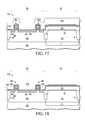
- FIG. 17is a cross section of another embodiment of a semiconductor structure having a non-volatile memory (NVM) structure and a logic transistor structure at an intermediate stage in processing according to another embodiment.
- NVMnon-volatile memory
- FIG. 18is a cross section of the semiconductor structure of FIG. 17 at a subsequent stage in processing.
- FIG. 19is a cross section of the semiconductor structure of FIG. 18 at a subsequent stage in processing.
- an integration of a non-volatile memory (NVM) cell in a NVM region of an integrated circuit and a logic transistor in a logic region of the integrated circuitincludes forming the gate structure of the NVM cell in the NVM region, including the charge storage layer, while masking the logic region.
- the logic gateis formed while masking the NVM region with a hard mask that is subsequently used to form sidewall spacers in the NVM region.
- the NVM cell(s) in the NVM regionare polished along with a logic gate in the logic region.
- the NVM cellsare protected using hard masks while the metal gate in the logic region is processed. Source/drain implants are performed simultaneously in the NVM and logic regions using the sidewall spacers as masks. This is better understood by reference to the drawings and the following written description.
- FIG. 1Shown in FIG. 1 is a semiconductor structure 100 of an integrated circuit having an NVM region 102 and a logic region 104 .
- Semiconductor structure 100has a substrate 106 , an isolation region 114 separating logic region 104 from NVM region 102 , an isolation region 112 in NVM region 102 that, along with isolation region 114 , defines borders of an active region in NVM region 102 , a P well 108 in substrate 106 in the NVM region 102 extending from the surface of substrate 106 , a P well 110 in logic region 104 that extends from the surface of substrate 106 , an N region 111 below P well 110 for aiding in providing noise isolation for the logic transistors, an oxide layer 118 on the top surface of substrate 106 in NVM region 102 and oxide or dielectric layer 120 on the top surface of substrate 106 in logic region 104 .
- Oxide or dielectric layer 120can be a thermal oxide that is grown, rather than deposited, for high quality electrical insulation. Isolation region 114
- a layer of polysilicon 122is deposited over oxide layers 118 , 120 and isolation regions 112 - 116 in NVM region 102 and logic region 104 .
- Polysilicon layer 122may be doped in situ or by implant 124 with an N-type material for forming N-channel transistors.
- N wellscan also be formed in other regions of logic region 104 , which are not shown, for the forming P channel transistors.
- the semiconductor substrate 106 described hereincan be any semiconductor material or combinations of materials, such as gallium arsenide, silicon germanium, silicon-on-insulator (SOI), silicon, monocrystalline silicon, the like, and combinations of the above.
- Oxide layerrefers to a silicon oxide layer or dielectric layer unless otherwise noted.
- nitride layerrefers to a silicon nitride layer unless otherwise noted.
- nitride layer 202also referred to as an optical patterning layer or cap layer
- a layer of oxidemay be deposited over polysilicon layer 122 instead of nitride layer 202 .
- Polysilicon layer 122 and nitride layer 202 in NVM region 102are patterned to form select gate structures 206 , 208 . Patterning is typically performed using patterned photoresist and etching unmasked regions of the photoresist. Recessed portions 204 of substrate 106 , also referred to as recessed trenches 204 , can be formed adjacent select gate structures 206 , 208 in NVM region 102 by removing regions of P well 108 in NVM region 102 during the etch.
- FIG. 3Shown in FIG. 3 is semiconductor structure 100 after a layer of repair oxide 302 , is grown in trenches 204 before P well 108 is counterdoped in the area below trenches 204 with N-type material 304 .
- Polysilicon layer 122 and nitride layer 202remain in logic region 104 while select gate structures 206 and 208 are formed through counterdoping of P well 108 .
- etch stop layer 402Shown in FIG. 4 is semiconductor structure 100 after an etch stop layer 402 and a layer of oxide 404 are conformally deposited over nitride layer 202 in NVM region 102 and logic region 104 .
- Etch stop layer 402can be formed of nitride or a material containing nitride.
- FIG. 5Shown in FIG. 5 is semiconductor structure 100 after nitride layer 202 , etch stop layer 402 and oxide 404 layer are partially removed and planarized using chemical mechanical polishing (CMP). Remaining portions of etch stop layer 402 and oxide layer 404 are shown as oxide portions 502 , 504 , 506 adjacent select gate structures 206 , 208 in NVM region 102 . A portion of nitride layer 202 remains at the top of the select gate structures 206 , 208 in NVM region 102 and over polysilicon layer 122 in logic region 104 after the CMP.
- CMPchemical mechanical polishing
- semiconductor structure 100after oxide portion 504 between select gate structures 206 , 208 is patterned and etched to form opening 606 between one side of oxide portion 504 and a first sidewall of select gate structure 206 and opening 608 between the another side of oxide portion 504 and a first sidewall of select gate structure 208 .
- Charge storage layer 602is formed in NVM region 102 and logic region 104 .
- Charge storage layer 602can be formed by first growing a thermal oxide layer on the exposed top surface of structures on substrate 106 including the top and some sides of oxide portions 502 , 504 , 506 , the top and some sides of select gate structures 206 , 208 as well as over nitride layer 128 in logic region 104 .
- This thermal oxide layermay be thinner over the nitride 202 remaining over select gate structures 206 , 208 and nitride 202 remaining over polysilicon layer 122 .
- the thermal oxide layer grown on the top surface of substrate 106is of particular importance because that is where charge will pass during program and erase.
- Nanocrystals or other charge storage layer(such as a layer of nitride) are formed on the grown oxide layer and a top oxide layer is deposited on and around the nanocrystals or other charge storage layer.
- Polysilicon layer 604is then deposited on charge storage layer 602 .
- control gate polysilicon regions 702remain adjacent select gate structures 206 , 208 and between regions of charge storage layer 602 .
- Polysilicon regions 702can be made conductive by in situ or implant doping with N-type material.
- Control gate polysilicon regions 702are recessed using an etch process.
- the height of control gate polysilicon regions 702 after recess etchingcan be below the height of polysilicon layers 122 of select gate structures 206 , 208 .
- Having the height of control gate polysilicon regions 702 below the height of select gate structures 206 , 208helps improve electrical isolation between control gate polysilicon regions 702 adjacent respective select gate structures 206 , 208 . This is due to the fact that any conductive artifacts remaining in the top of the oxide of charge storage layer 602 after the CMP will not form a conductive path between the top of control gate polysilicon regions 702 and respective select gate structures 206 , 208 . This improved isolation can be especially important during erase operations when the voltage differential between control gate polysilicon regions 702 and respective select gate structures 206 , 208 can be relatively high, such as approximately 14 Volts.
- FIG. 8Shown in FIG. 8 is semiconductor structure 100 after charge storage layer 602 and oxide portions 502 , 504 , 506 are patterned and etched, resulting in NVM structures 802 and 804 having control gate polysilicon regions 702 partially overlapping respective select gate structures 206 , 208 in NVM region 102 . Remaining sections of charge storage layer 602 partially overlap respective select gate structures 206 , 208 and are between select gate structures 206 , 208 and respective control gate polysilicon regions 702 . Charge storage layer 602 is also removed from logic region 104 .
- semiconductor structure 100after depositing protective layers in NVM region 102 and logic region 104 including an oxide layer 902 , a nitride layer 904 on oxide layer 902 , and an oxide layer 906 on nitride layer 904 .
- semiconductor structure 100after removing protective layers 902 , 904 , 906 , capping layer 202 , polysilicon layer 122 and oxide layer 120 from logic region 104 .
- the remaining region of protective layers 1002 over NVM region 102functions as a hard mask for the components in NVM region 102 .
- FIG. 11Shown in FIG. 11 is semiconductor structure 100 after forming a patterned logic control gate structure 1102 (also referred to as a sacrificial gate stack) in logic region 104 that includes a layer of grown oxide (not shown) over P well 110 , a layer of high-k dielectric 1104 over the oxide layer, a layer of barrier metal 1106 over the high-k dielectric 1104 , a layer of polysilicon 1108 (also referred to as a sacrificial control gate) over the barrier metal 1106 , and a cap layer 1110 (such as a nitride) over polysilicon 1108 .
- Oxide layer 906is removed during the cleaning process prior to growing the oxide (not shown) beneath the high-k dielectric layer 1104 .
- the etch of the barrier metal 1106 during the formation of logic gate structure 1102can have the effect of metal making contact with NVM region 102 , which can contaminate charge storage layer sections 602 ( FIG. 6 ), especially if charge storage layer 602 has nanocrystals.
- the hard mask formed by protective layer 1002prevents the nanocrystals or other charge storage layer or material from becoming contaminated.
- FIG. 12Shown in FIG. 12 is semiconductor structure 100 after a nitride layer 1202 and an oxide or dielectric layer 1204 is deposited on the substrate 106 over the NVM region and logic region 104 .
- nitride layer 1202is deposited on nitride layer 904 .
- Oxide layer 1204is on nitride layer 1202 .
- Oxide layer 1204 and nitride layer 1202are conformal.
- the oxide layer 1202is selectively removed from the NVM region 102 using a photo resist mask (not shown) to protect the logic region 104 , leaving the nitride layer 904 and 1202 exposed in the NVM region 102 .
- Nitride layers 904 and 1202can be removed with an isotropic etch, such as a hot phosphoric acid wet etch, which etches nitride selective to oxide, while the nitride layer 1202 remains on the logic region 104 since the nitride layer 1202 is protected by oxide layer 1204 as shown in FIG. 12 .
- an isotropic etchsuch as a hot phosphoric acid wet etch
- FIG. 13Shown in FIG. 13 is semiconductor structure 100 after performing an anisotropic etch of oxide layers 902 , 1204 and a subsequent etch of nitride layer 1202 that results in oxide layer 902 becoming sidewall spacers 902 around respective split gate NVM structures 802 , 804 in NVM region 102 .
- Sidewall spacer 902is adjacent to the select gate and an upper region of the control gate structure on one side and a lower region of the control gate on the other side of each NVM structure 802 , 804 .
- Sidewall spacer 902also surrounds an upper region of the control gate on one side of NVM structures 802 , 804 and is adjacent to a lower region of the control gate on one side and the select gate on the other side.
- nitride layer 1202becomes sidewall spacer or liner around logic structure 1102 and oxide layer 1204 becomes sidewall spacer around liner 1202 .
- Extension implants 1302may be utilized to dope the substrate 106 with implant material using spacers 902 , 1202 , 1204 as masks.
- Source/drain implants 1406may be formed for respective NVM structures 802 , 804 and logic structure 1102 using spacers 1402 , 1404 as masks. Source/drain implants 1406 are nearly aligned to opposing sides of respective NVM structures 802 , 804 and logic structure 1102 .
- the source/drain implants 1406 shownare N type. The exposed regions of source/drain implants 1406 and exposed polysilicon of select gates and control gates of respective NVM structures 802 , 804 and logic structure 1102 can then be silicided to make respective low resistance contacts 1408 .
- FIG. 15Shown in FIG. 15 is semiconductor structure 100 after an interlayer dielectric layer 1502 is deposited over NVM region 102 and logic region 104 and polished down using CMP to the top of select gates 122 in NVM region 102 and the top of polysilicon 1108 in logic structure 1102 . Note that a portion of charge storage layer 602 overlapping select gates 122 in NVM region 102 is removed during the CMP. Additionally, note that having the top of control gate regions 702 below the top of select gate 122 improves electrical isolation between control gate regions 702 and respective select gates 122 in NVM region.
- control gate region 702does get polished and thus eliminates susceptibility to control gate regions 702 to select gate region 122 electrical leakage due to conductive residual artifacts from the CMP which may conduct current between control gate regions 702 and respective select gates 122 when voltages are applied to control gate regions 702 and respective select gates 122 .
- hard mask 1508is formed over NVM region including a layer of nitride 1504 and a layer of oxide 1506 .
- FIG. 16Shown in FIG. 16 is semiconductor structure 100 after polysilicon gate 1108 is removed from logic structure 1102 using a wet etch to form a gate opening surrounded by first spacer 1202 for logic structure 1102 .
- a work function metal 1602is then deposited around the sides and bottom of the gate opening in logic structure 1102 .
- a gate metal 1604is then deposited over the work function metal 1602 to fill the gate opening.
- Combinations of work function metal 1602 and the barrier metal 1106sets the work function of N channel transistors and provides a highly conductive gate conductor in logic region 104 .
- An alternate combination of barrier metal and work function materialcan be used for P channel transistors.
- oxide layer 1506can be removed by CMP.
- An additional layer of interlayer dielectric(not shown) can be deposited over nitride layer 1504 in NVM region 102 and in logic region 104 . Openings (not shown) can be formed in dielectric 1502 and filled with conductive material to make contact with source/drain implants 1406 of NVM structures 802 , 804 and logic structure 1102 .
- FIG. 17is a cross section of another embodiment of a semiconductor structure 1700 having non-volatile memory (NVM) region 102 and logic region 104 at an intermediate stage in processing subsequent to the processing stage shown in FIG.
- NVMnon-volatile memory
- Charge storage layer 1702can be similar to charge storage layer 602 ( FIG. 6 ).
- FIG. 18is a cross section of the semiconductor structure 1700 of FIG. 16 at a subsequent stage in processing after polysilicon layer 1704 is reduced using a chemical mechanical polishing (CMP) process. Regions of polysilicon layer 1704 remain in NVM region 102 between isolation region 112 and select gate structure 1802 , between select gate structures 1802 and 1804 , and between select gate structure 1804 and polysilicon layer 122 in logic region 104 . Charge storage layer 1702 is between the select gate structures 1802 , 1804 and the regions of polysilicon layer 1704 and 122 . The regions of polysilicon layer 1704 can be recessed below the top of polysilicon 122 of select gate structures 1802 , 1804 to improve electrical isolation between polysilicon 122 and 1704 .
- CMPchemical mechanical polishing
- FIG. 19is a cross section of the semiconductor structure 1700 of FIG. 18 at a subsequent stage in processing after a patterned etch has been performed to remove segments of polysilicon layer 1704 to form the control gates and also to remove segments of charge storage layer 1702 , while leaving other segments of charge storage layer 1702 between respective select gate structures 1802 , 1804 and control gates 1704 .
- Charge storage segments 1702overlap the top of respective select gate structures 1802 , 1804 and underlie control gates 1704 adjacent substrate 106 to form completed split gate NVM cells 1902 , 1904 .
- Subsequent processing of semiconductor structure 1700 to form logic and/or I/O devices, such as logic structure 1102 ( FIG. 16 ), in logic region 104can follow the processes described herein for FIGS. 8 through 16 .
- metal gate transistorscan be made in the presence of NVM cells, even if the NVM cells use nanocrystals, and further that the hard mask used during the metal etch can also subsequently be used in forming sidewall spacers used as an implant mask.
- NVMnon-volatile memory
- a top surface of the control gatecan be lower than a top surface of the select gate and the charge storage layer is under the control gate, along adjacent sidewalls of the select gate and control gate, is partially over the top surface of the select gate.
- a second protection layer( 902 , 904 , 906 ) can be formed over the NVM region and the logic region. The second protection layer and the first protection layer are removed from the logic region leaving a portion of the second protection layer over the control gate and the select gate.
- a sacrificial gate stack ( 1102 )can be formed over the logic region comprising a gate dielectric ( 1202 ) of high k material and a sacrificial gate ( 1108 ) over the gate dielectric.
- a dielectric ( 1502 , 1402 , 1404 )can be formed around the sacrificial gate.
- the sacrificial gateis removed to leave an opening in the dielectric layer.
- a work function metal ( 1602 )is formed over the gate dielectric in the opening.
- a metal gate ( 1604 )is formed over the work function metal in the opening.
- the forming the control gate and the charge storage layercan comprise forming a dielectric layer ( 404 ) over the NVM region; forming an opening in the dielectric layer adjacent to the select gate; forming the charge storage layer ( 602 ) in the opening in the dielectric layer partially filling the opening in the dielectric layer; and forming the control gate in the opening in the dielectric layer over the charge storage layer; and removing the dielectric layer.
- the forming the control gate in the opening in the dielectric layer over the charge storage layercan be further characterized by depositing a layer of polysilicon ( 604 ) and etching back the polysilicon layer.
- control gate and the charge storage layercan be further characterized by the charge storage layer comprising nanocrystals.
- the forming the control gate and the charge storage layercan comprise: forming the charge storage layer over the NVM region including over the select gate; forming a polysilicon ( 1704 ) layer over the charge storage layer; etching the polysilicon layer so that a resulting top surface of the polysilicon layer can be below the top surface of the select gate; and patterning the polysilicon layer and the charge storage layer to leave a first portion of the charge storage layer adjacent to the select gate and a second portion extending laterally from the select gate and a portion of the polysilicon layer as the control gate over the second portion of the charge storage layer and adjacent to the first portion of the select gate.
- the charge storage layercan comprise nanocrystals.
- the methodfurther can comprise depositing a conformal layer over NVM region and the logic region; and etching the conformal layer to leave a first sidewall spacer around the logic gate and a second sidewall spacer around the control and select gate.
- the methodfurther can comprise performing an implant into the substrate using the first and second sidewall spacers as masks for the implant.
- the forming the second protection layer ( 1002 )can comprise forming a first oxide layer ( 902 ), a nitride layer ( 904 ) on the first oxide layer, and a second oxide layer ( 906 ) on the nitride layer.
- the step of forming the select gate and the protection layercan comprise: growing thermal oxide ( 118 ) on the substrate in NVM region; depositing a layer of polysilicon ( 122 ) over the thermal oxide; and patterning the layer of polysilicon to leave a portion of the layer of polysilicon as the select gate in the NVM region and the layer of polysilicon in the logic region as the protection layer.
- the methodfurther can comprise forming a capping layer ( 202 ) on the layer of polysilicon.
- the patterningcan be further characterized by patterning the capping layer with a same pattern as the layer of polysilicon is patterned.
- the second protection layercan comprise a first layer of oxide ( 902 ), a layer of nitride ( 104 ), and a second layer of oxide ( 106 ) on the layer of nitride.
- the forming the charge storage layer and the control gatefurther can comprise etching the charge storage layer to leave the top surface of the select gate partially covered with the charge storage layer.
- a method of making a semiconductor structure using a substrate ( 106 ) having a non-volatile memory (NVM) region ( 102 ) and a logic region ( 104 ),can comprise growing thermal oxide ( 118 ) on the substrate in the NVM region; forming a select gate ( 122 ) in the NVM region on the thermal oxide; counterdoping the substrate in the NVM region 9304 ) adjacent to the select gate; and forming a control gate ( 122 ) and a charge storage layer ( 602 ) over the substrate in the NVM region.
- NVMnon-volatile memory
- a top surface of the control gatecan be below a top surface of the select gate and the charge storage layer can be under the control gate, along adjacent sidewalls of the select gate and control gate, can be partially over the top surface of the select gate.
- a protective layer ( 1002 )can be formed over the NVM region and the logic region. The protective layer can be removed from the logic region.
- a gate structure ( 1102 )can be formed in the logic region comprising a high k dielectric ( 1106 ) as a gate dielectric and a sacrificial gate ( 1108 ) over the gate dielectric.
- a layer of dielectric material ( 1502 , 1402 , 1404 )can be formed around the gate structure. The sacrificial gate can be removed to leave an opening in the layer of dielectric material.
- a work function metal ( 1602 )can be formed in the opening.
- the protective layercan comprise a three layer stack ( 902 , 904 , 906 ) comprising oxide, nitride, and oxide.
- the forming the control gate and the charge storage layercan comprise: forming a dielectric layer ( 502 ) over the NVM region; forming an opening in the dielectric layer adjacent to the select gate; forming the charge storage layer in the opening in the dielectric layer partially filling the opening in the dielectric layer; forming the control gate in the opening in the dielectric layer over the charge storage layer; and removing the dielectric layer.
- the forming the control gate and the charge storage layercan comprise: forming the charge storage layer over the NVM region including over the select gate; forming a polysilicon layer ( 1704 ) over the charge storage layer; etching back the polysilicon layer so that a resulting top surface of the polysilicon layer can be below the top surface of the select gate; and patterning the polysilicon layer and the charge storage layer to leave a first portion of the charge storage layer adjacent to the select gate and a second portion extending laterally from the select gate and a portion of the polysilicon layer as the control gate over the second portion of the charge storage layer and adjacent to the first portion of the select gate.
- the forming the layer of dielectric materialcan comprise forming a first sidewall spacer ( 1602 ) around the gate stack and forming an interlayer dielectric around the first sidewall spacer.
- a semiconductor structure using a substrate having a non-volatile memory (NVM) region ( 102 ) and a logic region ( 104 )can comprise a select gate ( 122 ) comprising polysilicon over a thermal oxide layer ( 118 ) on the substrate ( 106 ) in the NVM region; a control gate ( 702 ) adjacent a first side of the select gate and having a top surface below a top surface of the select gate; a charge storage layer ( 602 ) having a first portion between the control gate and the substrate, a second portion between the control gate and the first side of the select gate, and a third portion partially over the select gate; and a logic gate ( 1602 , 1604 ) comprising metal over a high k dielectric ( 1204 ) over the substrate in the logic region.
- NVMnon-volatile memory
- the logic gatecan comprise a work function metal ( 1602 ) over the high k dielectric and a gate metal ( 1604 ) over the work function metal different from the work function metal.
- Coupledis not intended to be limited to a direct coupling or a mechanical coupling.
Landscapes
- Engineering & Computer Science (AREA)
- Manufacturing & Machinery (AREA)
- Non-Volatile Memory (AREA)
- Semiconductor Memories (AREA)
Abstract
Description
Claims (18)
Priority Applications (1)
| Application Number | Priority Date | Filing Date | Title |
|---|---|---|---|
| US14/041,662US8901632B1 (en) | 2013-09-30 | 2013-09-30 | Non-volatile memory (NVM) and high-K and metal gate integration using gate-last methodology |
Applications Claiming Priority (1)
| Application Number | Priority Date | Filing Date | Title |
|---|---|---|---|
| US14/041,662US8901632B1 (en) | 2013-09-30 | 2013-09-30 | Non-volatile memory (NVM) and high-K and metal gate integration using gate-last methodology |
Publications (1)
| Publication Number | Publication Date |
|---|---|
| US8901632B1true US8901632B1 (en) | 2014-12-02 |
Family
ID=51948355
Family Applications (1)
| Application Number | Title | Priority Date | Filing Date |
|---|---|---|---|
| US14/041,662ActiveUS8901632B1 (en) | 2013-09-30 | 2013-09-30 | Non-volatile memory (NVM) and high-K and metal gate integration using gate-last methodology |
Country Status (1)
| Country | Link |
|---|---|
| US (1) | US8901632B1 (en) |
Cited By (21)
| Publication number | Priority date | Publication date | Assignee | Title |
|---|---|---|---|---|
| US20140252445A1 (en)* | 2013-03-07 | 2014-09-11 | Globalfoundries Singapore Pte. Ltd. | Method of forming split-gate cell for non-volative memory devices |
| US20150054044A1 (en)* | 2013-08-22 | 2015-02-26 | Freescale Semiconductor, Inc | Method to Form a Polysilicon Nanocrystal Thin Film Storage Bitcell within a High K Metal Gate Platform Technology Using a Gate Last Process to Form Transistor Gates |
| US20150093864A1 (en)* | 2013-09-30 | 2015-04-02 | Freescale Semiconductor, Inc. | Non-volatile memory (nvm) and high-k and metal gate integration using gate-last methodology |
| US20150145022A1 (en)* | 2013-11-27 | 2015-05-28 | Taiwan Semiconductor Manufacturing Co., Ltd. | Cmp fabrication solution for split gate memory embedded in hk-mg process |
| US9082650B2 (en) | 2013-08-21 | 2015-07-14 | Freescale Semiconductor, Inc. | Integrated split gate non-volatile memory cell and logic structure |
| US9082837B2 (en) | 2013-08-08 | 2015-07-14 | Freescale Semiconductor, Inc. | Nonvolatile memory bitcell with inlaid high k metal select gate |
| US9087913B2 (en) | 2012-04-09 | 2015-07-21 | Freescale Semiconductor, Inc. | Integration technique using thermal oxide select gate dielectric for select gate and apartial replacement gate for logic |
| US20150279853A1 (en)* | 2014-03-28 | 2015-10-01 | Mark D. Hall | Method for forming a split-gate device |
| US20150348984A1 (en)* | 2014-05-30 | 2015-12-03 | SanDisk Technologies, Inc. | Method of making a monolithic three dimensional nand string using a select gate etch stop layer |
| US20160020219A1 (en)* | 2014-07-16 | 2016-01-21 | Taiwan Semiconductor Manufacturing Co., Ltd. | Recess technique to embed flash memory in soi technology |
| US9252246B2 (en) | 2013-08-21 | 2016-02-02 | Freescale Semiconductor, Inc. | Integrated split gate non-volatile memory cell and logic device |
| US9257445B2 (en)* | 2014-05-30 | 2016-02-09 | Freescale Semiconductor, Inc. | Method of making a split gate non-volatile memory (NVM) cell and a logic transistor |
| US9583640B1 (en)* | 2015-12-29 | 2017-02-28 | Globalfoundries Inc. | Method including a formation of a control gate of a nonvolatile memory cell and semiconductor structure |
| US9837425B2 (en) | 2016-04-19 | 2017-12-05 | United Microelectronics Corp. | Semiconductor device with split gate flash memory cell structure and method of manufacturing the same |
| US20180158833A1 (en)* | 2016-05-16 | 2018-06-07 | Globalfoundries Inc. | Semiconductor structure including a plurality of pairs of nonvolatile memory cells and an edge cell |
| WO2019018231A1 (en)* | 2017-07-19 | 2019-01-24 | Cypress Semiconductor Corporation | Embedded non-volatile memory device and fabrication method of the same |
| US10332884B2 (en)* | 2017-11-02 | 2019-06-25 | United Microelectronics Corp. | FinFET semiconductor device |
| US20200006365A1 (en)* | 2017-07-28 | 2020-01-02 | Taiwan Semiconductor Manufacturing Co., Ltd. | Seal method to integrate non-volatile memory (nvm) into logic or bipolar cmos dmos (bcd) technology |
| US10916555B2 (en) | 2019-01-31 | 2021-02-09 | United Microelectronics Corp. | Structure of memory cell and method for fabricating the same |
| US20220336481A1 (en)* | 2019-12-13 | 2022-10-20 | Winbond Electronics Corp. | Manufacturing method of semiconductor device |
| US20230320089A1 (en)* | 2017-07-28 | 2023-10-05 | Taiwan Semiconductor Manufacturing Company, Ltd. | Seal method to integrate non-volatile memory (nvm) into logic or bipolar cmos dmos (bcd) technology |
Citations (114)
| Publication number | Priority date | Publication date | Assignee | Title |
|---|---|---|---|---|
| US5614746A (en) | 1994-11-28 | 1997-03-25 | United Microelectronics Corporation | Structure and process of manufacture of split gate flash memory cell |
| US6087225A (en) | 1998-02-05 | 2000-07-11 | International Business Machines Corporation | Method for dual gate oxide dual workfunction CMOS |
| US6194301B1 (en) | 1999-07-12 | 2001-02-27 | International Business Machines Corporation | Method of fabricating an integrated circuit of logic and memory using damascene gate structure |
| US6235574B1 (en) | 1999-03-22 | 2001-05-22 | Infineon North America Corp. | High performance DRAM and method of manufacture |
| US20010049166A1 (en) | 2000-03-29 | 2001-12-06 | Stmicroelectronics S.R.L. | Method of manufacturing an electrically programmable, non-volatile memory and high-performance logic circuitry in the same semiconductor chip |
| US6333223B1 (en) | 1998-12-25 | 2001-12-25 | Matsushita Electric Industrial Co., Ltd. | Semiconductor device and method of manufacturing the same |
| US20020061616A1 (en) | 2000-11-22 | 2002-05-23 | Kim Jae Hyung | Method for fabricating semiconductor device |
| US20030022434A1 (en) | 1998-12-25 | 2003-01-30 | Yasuhiro Taniguchi | Semiconductor integrated circuit device and a method of manufacturing the same |
| US6531734B1 (en) | 2002-05-24 | 2003-03-11 | Silicon Based Technology Corp. | Self-aligned split-gate flash memory cell having an integrated source-side erase structure and its contactless flash memory arrays |
| US6635526B1 (en) | 2002-06-07 | 2003-10-21 | Infineon Technologies Ag | Structure and method for dual work function logic devices in vertical DRAM process |
| US6707079B2 (en) | 2001-02-22 | 2004-03-16 | Halo Lsi, Inc. | Twin MONOS cell fabrication method and array organization |
| US20040075133A1 (en) | 2000-09-29 | 2004-04-22 | Fujitsu Limited | Semiconductor device and its manufacturing method |
| US6777761B2 (en) | 2002-08-06 | 2004-08-17 | International Business Machines Corporation | Semiconductor chip using both polysilicon and metal gate devices |
| US6785165B2 (en) | 2002-01-25 | 2004-08-31 | Renesas Technology Corporation | Semiconductor device |
| US20040262670A1 (en) | 2003-06-30 | 2004-12-30 | Kabushiki Kaisha Toshiba | Semiconductor device including nonvolatile memory and method for fabricating the same |
| US20050145949A1 (en) | 2003-10-27 | 2005-07-07 | Kayvan Sadra | Application of different isolation schemes for logic and embedded memory |
| US6939767B2 (en) | 2003-11-19 | 2005-09-06 | Freescale Semiconductor, Inc. | Multi-bit non-volatile integrated circuit memory and method therefor |
| US20060038240A1 (en) | 2004-08-17 | 2006-02-23 | Fujitsu Limited | Semiconductor device and manufacturing method of the same |
| US20060046449A1 (en) | 2004-08-27 | 2006-03-02 | Taiwan Semiconductor Manufacturing Co., Ltd. | Metal gate structure for mos devices |
| US20060099798A1 (en) | 2004-11-08 | 2006-05-11 | Fujitsu Limited | Semiconductor device and manufacturing method of the same |
| US20060134864A1 (en) | 2004-12-22 | 2006-06-22 | Masaaki Higashitani | Multi-thickness dielectric for semiconductor memory |
| US20060211206A1 (en) | 2005-03-18 | 2006-09-21 | Freescale Semiconductor, Inc. | Electronic devices including non-volatile memory and processes for forming the same |
| US20060221688A1 (en) | 1999-02-01 | 2006-10-05 | Shoji Shukuri | Semiconductor integrated circuit and nonvolatile memory element |
| US7154779B2 (en) | 2004-01-21 | 2006-12-26 | Sandisk Corporation | Non-volatile memory cell using high-k material inter-gate programming |
| US20070037343A1 (en) | 2005-08-10 | 2007-02-15 | Texas Instruments Inc. | Process for manufacturing dual work function metal gates in a microelectronics device |
| US7183159B2 (en) | 2005-01-14 | 2007-02-27 | Freescale Semiconductor, Inc. | Method of forming an integrated circuit having nanocluster devices and non-nanocluster devices |
| US7190022B2 (en) | 2003-06-27 | 2007-03-13 | Infineon Technologies Ag | One transistor flash memory cell |
| US20070077705A1 (en) | 2005-09-30 | 2007-04-05 | Prinz Erwin J | Split gate memory cell and method therefor |
| US7202524B2 (en) | 2004-12-08 | 2007-04-10 | Samsung Electronics Co., Ltd. | Nonvolatile memory device and method of manufacturing the same |
| US7208793B2 (en) | 2004-11-23 | 2007-04-24 | Micron Technology, Inc. | Scalable integrated logic and non-volatile memory |
| US20070115725A1 (en) | 2004-12-22 | 2007-05-24 | Tuan Pham | Low-Voltage, Multiple Thin-Gate Oxide and Low-Resistance Gate Electrode |
| US7256125B2 (en) | 2003-08-25 | 2007-08-14 | Renesas Technology Corp. | Method of manufacturing a semiconductor device |
| US7271050B2 (en) | 2002-08-27 | 2007-09-18 | Micron Technology, Inc. | Silicon nanocrystal capacitor and process for forming same |
| US20070215917A1 (en) | 2006-03-20 | 2007-09-20 | Renesas Technology Corp. | Semiconductor integrated circuit device and a method of manufacturing the same |
| US20070224772A1 (en) | 2006-03-21 | 2007-09-27 | Freescale Semiconductor, Inc. | Method for forming a stressor structure |
| US20070249129A1 (en) | 2006-04-21 | 2007-10-25 | Freescale Semiconductor, Inc. | STI stressor integration for minimal phosphoric exposure and divot-free topography |
| US20070264776A1 (en) | 2003-11-19 | 2007-11-15 | Zhong Dong | Precision creation of inter-gates insulator |
| US20080029805A1 (en) | 2006-08-03 | 2008-02-07 | Yasuhiro Shimamoto | Semiconductor device and manufacturing method of the same |
| US20080050875A1 (en) | 2006-08-25 | 2008-02-28 | Jung-Ho Moon | Methods of fabricating embedded flash memory devices |
| US20080067599A1 (en) | 2005-05-23 | 2008-03-20 | Fujitsu Limited | Semiconductor device and method of manufacturing the same |
| US7365389B1 (en) | 2004-12-10 | 2008-04-29 | Spansion Llc | Memory cell having enhanced high-K dielectric |
| US20080105945A1 (en) | 2004-11-12 | 2008-05-08 | Freescale Semiconductor, Inc. | Method of forming a nanocluster charge storage device |
| US20080121983A1 (en) | 2006-09-22 | 2008-05-29 | Seong Geum-Jung | Gate and method of forming the same, and memory device and method of manufacturing the same |
| US20080128785A1 (en) | 2006-11-30 | 2008-06-05 | Jin-Ha Park | Flash memory device and method of manufacturing the same |
| US20080145985A1 (en) | 2006-12-15 | 2008-06-19 | Semiconductor Manufacturing International (Shanghai) Corporation | Embedded semiconductor memory devices and methods for fabricating the same |
| US7391075B2 (en) | 2004-10-08 | 2008-06-24 | Samsung Electronics Co., Ltd. | Non-volatile semiconductor memory device with alternative metal gate material |
| US7402493B2 (en) | 2004-04-12 | 2008-07-22 | Samsung Electronics Co., Ltd. | Method for forming non-volatile memory devices |
| US20080185635A1 (en) | 2007-02-01 | 2008-08-07 | Renesas Technology Corp. | Semiconductor storage device and manufacturing method thereof |
| US20080237690A1 (en) | 2007-03-26 | 2008-10-02 | Fujitsu Limited | Semiconductor device and method of manufacturing the same |
| US20080237700A1 (en) | 2007-03-28 | 2008-10-02 | Samsung Electronics Co., Ltd. | Nonvolatile memory device having cell and peripheral regions and method of making the same |
| US7439134B1 (en) | 2007-04-20 | 2008-10-21 | Freescale Semiconductor, Inc. | Method for process integration of non-volatile memory cell transistors with transistors of another type |
| US20080283900A1 (en) | 2005-12-14 | 2008-11-20 | Fujitsu Limited | Semiconductor device and method for manufacturing the same |
| US20080290385A1 (en) | 2007-05-24 | 2008-11-27 | Seiko Epson Corporation | Method for manufacturing ferroelectric capacitor, and ferroelectric capacitor |
| US20080308876A1 (en) | 2007-06-12 | 2008-12-18 | Hye-Lan Lee | Semiconductor device and method of manufacturing the same |
| US20090050955A1 (en) | 2007-08-24 | 2009-02-26 | Kenichi Akita | Nonvolatile semiconductor device and method of manufacturing the same |
| US20090065845A1 (en) | 2007-09-11 | 2009-03-12 | Samsung Electronics Co., Ltd. | Embedded semiconductor device and method of manufacturing an embedded semiconductor device |
| US20090072274A1 (en) | 2007-09-14 | 2009-03-19 | Qimonda Ag | Integrated circuit including a first gate stack and a second gate stack and a method of manufacturing |
| US20090078986A1 (en) | 2007-09-20 | 2009-03-26 | Lars Bach | Manufacturing method for an integrated circuit including different types of gate stacks, corresponding intermediate integrated circuit structure and corresponding integrated circuit |
| US7521314B2 (en) | 2007-04-20 | 2009-04-21 | Freescale Semiconductor, Inc. | Method for selective removal of a layer |
| US20090101961A1 (en) | 2007-10-22 | 2009-04-23 | Yue-Song He | Memory devices with split gate and blocking layer |
| US7524719B2 (en) | 2006-08-31 | 2009-04-28 | Freescale Semiconductor, Inc. | Method of making self-aligned split gate memory cell |
| US20090111229A1 (en)* | 2007-10-31 | 2009-04-30 | Steimle Robert F | Method of forming a split gate non-volatile memory cell |
| WO2009058486A1 (en) | 2007-10-29 | 2009-05-07 | Freescale Semiconductor Inc. | Method for integrating nvm circuitry with logic circuitry |
| US7544490B2 (en) | 2002-02-08 | 2009-06-09 | Genencor International, Inc. | Secretion, transcription and sporulation genes in Bacillus clausii |
| US7544980B2 (en) | 2006-01-27 | 2009-06-09 | Freescale Semiconductor, Inc. | Split gate memory cell in a FinFET |
| US7560767B2 (en) | 2005-10-14 | 2009-07-14 | Kabushiki Kaisha Toshiba | Nonvolatile semiconductor memory device |
| US20090179283A1 (en) | 2007-12-12 | 2009-07-16 | International Business Machines Corporation | Metal gate stack and semiconductor gate stack for cmos devices |
| US20090225602A1 (en) | 2005-05-26 | 2009-09-10 | Micron Technology, Inc. | Multi-state memory cell |
| US20090256211A1 (en) | 2008-04-10 | 2009-10-15 | International Business Machines Corporation | Metal gate compatible flash memory gate stack |
| US20090269893A1 (en) | 2001-07-05 | 2009-10-29 | Fujitsu Limited | Semiconductor integrated circuit device and method of producing the same |
| US20090273013A1 (en) | 2008-04-30 | 2009-11-05 | Winstead Brian A | Method of forming a split gate memory device and apparatus |
| US20090278187A1 (en) | 2008-05-09 | 2009-11-12 | Toba Takayuki | Semiconductor device and manufacturing method of semiconductor device |
| US7799650B2 (en) | 2007-08-08 | 2010-09-21 | Freescale Semiconductor, Inc. | Method for making a transistor with a stressor |
| US7816727B2 (en) | 2007-08-27 | 2010-10-19 | Macronix International Co., Ltd. | High-κ capped blocking dielectric bandgap engineered SONOS and MONOS |
| US7821055B2 (en) | 2009-03-31 | 2010-10-26 | Freescale Semiconductor, Inc. | Stressed semiconductor device and method for making |
| US20110031548A1 (en) | 2008-04-15 | 2011-02-10 | Freescale Semiconductor, Inc. | Split gate non-volatile memory cell with improved endurance and method therefor |
| US7906396B1 (en) | 2009-09-02 | 2011-03-15 | Winbond Electronics Corp. | Flash memory and method of fabricating the same |
| US7932146B2 (en) | 2008-03-20 | 2011-04-26 | United Microelectronics Corp. | Metal gate transistor and polysilicon resistor and method for fabricating the same |
| US20110095348A1 (en) | 2009-10-28 | 2011-04-28 | Renesas Electronics Corporation | Semiconductor device and method of manufacturing the same |
| US7989871B2 (en) | 2006-03-15 | 2011-08-02 | Kabushiki Kaisha Toshiba | Nonvolatile semiconductor memory device having insulating films that include multiple layers formed by insulating materials having d-orbital metal element and insulating materials without d-orbital metal element |
| US7999304B2 (en) | 2007-02-07 | 2011-08-16 | Kabushiki Kaisha Toshiba | Semiconductor device |
| US20110204450A1 (en) | 2010-02-25 | 2011-08-25 | Renesas Electronics Corporation | Semiconductor device and manufacturing method thereof |
| US8017991B2 (en) | 2006-07-28 | 2011-09-13 | Samsung Electronics Co., Ltd. | Non-volatile memory device and methods of operating and fabricating the same |
| US8043951B2 (en) | 2007-08-01 | 2011-10-25 | Freescale Semiconductor, Inc. | Method of manufacturing a semiconductor device and semiconductor device obtainable therewith |
| US20110260258A1 (en) | 2009-12-31 | 2011-10-27 | Institute of Microelectronics, Chinese Academy of Sciences | Field effect transistor device with improved carrier mobility and method of manufacturing the same |
| US8063434B1 (en) | 2007-05-25 | 2011-11-22 | Cypress Semiconductor Corporation | Memory transistor with multiple charge storing layers and a high work function gate electrode |
| US8093128B2 (en) | 2007-05-25 | 2012-01-10 | Cypress Semiconductor Corporation | Integration of non-volatile charge trap memory devices and logic CMOS devices |
| US20120034751A1 (en) | 2010-08-06 | 2012-02-09 | Fujitsu Semiconductor Limited | Method of manufacturing semiconductor device |
| US8138037B2 (en) | 2009-03-17 | 2012-03-20 | International Business Machines Corporation | Method and structure for gate height scaling with high-k/metal gate technology |
| US8168493B2 (en) | 2010-03-05 | 2012-05-01 | Samsung Electronics Co., Ltd. | Semiconductor memory device and method of manufacturing the same |
| US20120104483A1 (en) | 2010-10-29 | 2012-05-03 | Shroff Mehul D | Non-volatile memory and logic circuit process integration |
| US20120132978A1 (en) | 2010-11-25 | 2012-05-31 | Renesas Electronics Corporation | Semiconductor device and manufacturing method of semiconductor device |
| US20120142153A1 (en) | 2005-03-08 | 2012-06-07 | Magnachip Semiconductor Ltd. | Non-volatile memory device and method for fabricating the same |
| US20120252171A1 (en)* | 2011-03-31 | 2012-10-04 | Shroff Mehul D | Non-volatile memory and logic circuit process integration |
| US20120248523A1 (en) | 2011-03-31 | 2012-10-04 | Shroff Mehul D | Non-volatile memory and logic circuit process integration |
| US8298885B2 (en) | 2009-05-15 | 2012-10-30 | Globalfoundries Inc. | Semiconductor device comprising metal gates and a silicon containing resistor formed on an isolation structure |
| US8334198B2 (en) | 2011-04-12 | 2012-12-18 | Taiwan Semiconductor Manufacturing Company, Ltd. | Method of fabricating a plurality of gate structures |
| US20130026553A1 (en) | 2011-07-26 | 2013-01-31 | Synopsys, Inc. | NVM Bitcell with a Replacement Control Gate and Additional Floating Gate |
| US8372699B2 (en) | 2010-02-22 | 2013-02-12 | Freescale Semiconductor, Inc. | Method for forming a split-gate memory cell |
| US20130037886A1 (en) | 2011-08-10 | 2013-02-14 | Teng-Chun Tsai | Semiconductor device and method of making the same |
| US20130065366A1 (en) | 2011-09-08 | 2013-03-14 | Stmicroelectronics | Soi integrated circuit comprising adjacent cells of different types |
| US20130084684A1 (en) | 2011-10-03 | 2013-04-04 | Renesas Electronics Corporation | Manufacturing method of semiconductor device |
| US20130137227A1 (en) | 2011-11-30 | 2013-05-30 | Mehul D. Shroff | Logic and non-volatile memory (nvm) integration |
| US20130171786A1 (en) | 2012-01-04 | 2013-07-04 | Freescale Semiconductor, Inc. | Non-volatile memory (nvm) and logic integration |
| US20130171785A1 (en) | 2012-01-04 | 2013-07-04 | Mehul D. Shroff | Non-volatile memory (nvm) and logic integration |
| US20130178027A1 (en) | 2012-01-04 | 2013-07-11 | Freescale Semiconductor, Inc. | Non-volatile memory (nvm) and logic integration |
| US8524557B1 (en) | 2012-02-22 | 2013-09-03 | Freescale Semiconductor, Inc. | Integration technique using thermal oxide select gate dielectric for select gate and replacement gate for logic |
| US20130267074A1 (en) | 2012-04-09 | 2013-10-10 | Freescale Semiconductor Inc. | Integration technique using thermal oxide select gate dielectric for select gate and apartial replacement gate for logic |
| US20130267072A1 (en)* | 2012-04-06 | 2013-10-10 | Freescale Semiconductor, Inc. | Non-volatile memory (nvm) and logic integration |
| US20130264633A1 (en) | 2012-04-09 | 2013-10-10 | Mark D. Hall | Logic transistor and non-volatile memory cell integration |
| US20130323922A1 (en) | 2011-09-29 | 2013-12-05 | Freescale Semiconductor, Inc. | Split gate memory device with gap spacer |
| US20140035027A1 (en) | 2009-11-25 | 2014-02-06 | Renesas Electronics Corporation | Semiconductor device and a manufacturing method thereof |
| US20140050029A1 (en) | 2012-08-20 | 2014-02-20 | Sung-taeg Kang | Split-gate memory cells having select-gate sidewall metal silicide regions and related manufacturing methods |
| US20140120713A1 (en) | 2012-10-26 | 2014-05-01 | Mehul D. Shroff | Method of making a logic transistor and a non-volatile memory (nvm) cell |
- 2013
- 2013-09-30USUS14/041,662patent/US8901632B1/enactiveActive
Patent Citations (127)
| Publication number | Priority date | Publication date | Assignee | Title |
|---|---|---|---|---|
| US5614746A (en) | 1994-11-28 | 1997-03-25 | United Microelectronics Corporation | Structure and process of manufacture of split gate flash memory cell |
| US6087225A (en) | 1998-02-05 | 2000-07-11 | International Business Machines Corporation | Method for dual gate oxide dual workfunction CMOS |
| US6333223B1 (en) | 1998-12-25 | 2001-12-25 | Matsushita Electric Industrial Co., Ltd. | Semiconductor device and method of manufacturing the same |
| US6509225B2 (en) | 1998-12-25 | 2003-01-21 | Matsushita Electric Industrial Co., Ltd. | Semiconductor device and method of manufacturing the same |
| US20030022434A1 (en) | 1998-12-25 | 2003-01-30 | Yasuhiro Taniguchi | Semiconductor integrated circuit device and a method of manufacturing the same |
| US20060221688A1 (en) | 1999-02-01 | 2006-10-05 | Shoji Shukuri | Semiconductor integrated circuit and nonvolatile memory element |
| US6235574B1 (en) | 1999-03-22 | 2001-05-22 | Infineon North America Corp. | High performance DRAM and method of manufacture |
| US6194301B1 (en) | 1999-07-12 | 2001-02-27 | International Business Machines Corporation | Method of fabricating an integrated circuit of logic and memory using damascene gate structure |
| US6388294B1 (en) | 1999-07-12 | 2002-05-14 | International Business Machines Corporation | Integrated circuit using damascene gate structure |
| US20010049166A1 (en) | 2000-03-29 | 2001-12-06 | Stmicroelectronics S.R.L. | Method of manufacturing an electrically programmable, non-volatile memory and high-performance logic circuitry in the same semiconductor chip |
| US7476582B2 (en) | 2000-09-29 | 2009-01-13 | Fujitsu Limited | Semiconductor device and its manufacturing method |
| US20040075133A1 (en) | 2000-09-29 | 2004-04-22 | Fujitsu Limited | Semiconductor device and its manufacturing method |
| US20020061616A1 (en) | 2000-11-22 | 2002-05-23 | Kim Jae Hyung | Method for fabricating semiconductor device |
| US6707079B2 (en) | 2001-02-22 | 2004-03-16 | Halo Lsi, Inc. | Twin MONOS cell fabrication method and array organization |
| US20090269893A1 (en) | 2001-07-05 | 2009-10-29 | Fujitsu Limited | Semiconductor integrated circuit device and method of producing the same |
| US6785165B2 (en) | 2002-01-25 | 2004-08-31 | Renesas Technology Corporation | Semiconductor device |
| US7544490B2 (en) | 2002-02-08 | 2009-06-09 | Genencor International, Inc. | Secretion, transcription and sporulation genes in Bacillus clausii |
| US6531734B1 (en) | 2002-05-24 | 2003-03-11 | Silicon Based Technology Corp. | Self-aligned split-gate flash memory cell having an integrated source-side erase structure and its contactless flash memory arrays |
| US6635526B1 (en) | 2002-06-07 | 2003-10-21 | Infineon Technologies Ag | Structure and method for dual work function logic devices in vertical DRAM process |
| US6777761B2 (en) | 2002-08-06 | 2004-08-17 | International Business Machines Corporation | Semiconductor chip using both polysilicon and metal gate devices |
| US7271050B2 (en) | 2002-08-27 | 2007-09-18 | Micron Technology, Inc. | Silicon nanocrystal capacitor and process for forming same |
| US7190022B2 (en) | 2003-06-27 | 2007-03-13 | Infineon Technologies Ag | One transistor flash memory cell |
| US20040262670A1 (en) | 2003-06-30 | 2004-12-30 | Kabushiki Kaisha Toshiba | Semiconductor device including nonvolatile memory and method for fabricating the same |
| US7256125B2 (en) | 2003-08-25 | 2007-08-14 | Renesas Technology Corp. | Method of manufacturing a semiconductor device |
| US20050145949A1 (en) | 2003-10-27 | 2005-07-07 | Kayvan Sadra | Application of different isolation schemes for logic and embedded memory |
| US20070264776A1 (en) | 2003-11-19 | 2007-11-15 | Zhong Dong | Precision creation of inter-gates insulator |
| US6939767B2 (en) | 2003-11-19 | 2005-09-06 | Freescale Semiconductor, Inc. | Multi-bit non-volatile integrated circuit memory and method therefor |
| US7405968B2 (en) | 2004-01-21 | 2008-07-29 | Sandisk Corporation | Non-volatile memory cell using high-K material and inter-gate programming |
| US7154779B2 (en) | 2004-01-21 | 2006-12-26 | Sandisk Corporation | Non-volatile memory cell using high-k material inter-gate programming |
| US7402493B2 (en) | 2004-04-12 | 2008-07-22 | Samsung Electronics Co., Ltd. | Method for forming non-volatile memory devices |
| US20060038240A1 (en) | 2004-08-17 | 2006-02-23 | Fujitsu Limited | Semiconductor device and manufacturing method of the same |
| US20060046449A1 (en) | 2004-08-27 | 2006-03-02 | Taiwan Semiconductor Manufacturing Co., Ltd. | Metal gate structure for mos devices |
| US7391075B2 (en) | 2004-10-08 | 2008-06-24 | Samsung Electronics Co., Ltd. | Non-volatile semiconductor memory device with alternative metal gate material |
| US20060099798A1 (en) | 2004-11-08 | 2006-05-11 | Fujitsu Limited | Semiconductor device and manufacturing method of the same |
| US20080105945A1 (en) | 2004-11-12 | 2008-05-08 | Freescale Semiconductor, Inc. | Method of forming a nanocluster charge storage device |
| US7544990B2 (en) | 2004-11-23 | 2009-06-09 | Micron Technology, Inc. | Scalable integrated logic and non-volatile memory |
| US7208793B2 (en) | 2004-11-23 | 2007-04-24 | Micron Technology, Inc. | Scalable integrated logic and non-volatile memory |
| US7202524B2 (en) | 2004-12-08 | 2007-04-10 | Samsung Electronics Co., Ltd. | Nonvolatile memory device and method of manufacturing the same |
| US7365389B1 (en) | 2004-12-10 | 2008-04-29 | Spansion Llc | Memory cell having enhanced high-K dielectric |
| US20060134864A1 (en) | 2004-12-22 | 2006-06-22 | Masaaki Higashitani | Multi-thickness dielectric for semiconductor memory |
| US20070115725A1 (en) | 2004-12-22 | 2007-05-24 | Tuan Pham | Low-Voltage, Multiple Thin-Gate Oxide and Low-Resistance Gate Electrode |
| US7183159B2 (en) | 2005-01-14 | 2007-02-27 | Freescale Semiconductor, Inc. | Method of forming an integrated circuit having nanocluster devices and non-nanocluster devices |
| US20120142153A1 (en) | 2005-03-08 | 2012-06-07 | Magnachip Semiconductor Ltd. | Non-volatile memory device and method for fabricating the same |
| US20060211206A1 (en) | 2005-03-18 | 2006-09-21 | Freescale Semiconductor, Inc. | Electronic devices including non-volatile memory and processes for forming the same |
| US20080067599A1 (en) | 2005-05-23 | 2008-03-20 | Fujitsu Limited | Semiconductor device and method of manufacturing the same |
| US20090225602A1 (en) | 2005-05-26 | 2009-09-10 | Micron Technology, Inc. | Multi-state memory cell |
| US20070037343A1 (en) | 2005-08-10 | 2007-02-15 | Texas Instruments Inc. | Process for manufacturing dual work function metal gates in a microelectronics device |
| US20070077705A1 (en) | 2005-09-30 | 2007-04-05 | Prinz Erwin J | Split gate memory cell and method therefor |
| US7560767B2 (en) | 2005-10-14 | 2009-07-14 | Kabushiki Kaisha Toshiba | Nonvolatile semiconductor memory device |
| US20080283900A1 (en) | 2005-12-14 | 2008-11-20 | Fujitsu Limited | Semiconductor device and method for manufacturing the same |
| US7544980B2 (en) | 2006-01-27 | 2009-06-09 | Freescale Semiconductor, Inc. | Split gate memory cell in a FinFET |
| US7989871B2 (en) | 2006-03-15 | 2011-08-02 | Kabushiki Kaisha Toshiba | Nonvolatile semiconductor memory device having insulating films that include multiple layers formed by insulating materials having d-orbital metal element and insulating materials without d-orbital metal element |
| US20070215917A1 (en) | 2006-03-20 | 2007-09-20 | Renesas Technology Corp. | Semiconductor integrated circuit device and a method of manufacturing the same |
| US20070224772A1 (en) | 2006-03-21 | 2007-09-27 | Freescale Semiconductor, Inc. | Method for forming a stressor structure |
| US20070249129A1 (en) | 2006-04-21 | 2007-10-25 | Freescale Semiconductor, Inc. | STI stressor integration for minimal phosphoric exposure and divot-free topography |
| US8017991B2 (en) | 2006-07-28 | 2011-09-13 | Samsung Electronics Co., Ltd. | Non-volatile memory device and methods of operating and fabricating the same |
| US20080029805A1 (en) | 2006-08-03 | 2008-02-07 | Yasuhiro Shimamoto | Semiconductor device and manufacturing method of the same |
| US20080050875A1 (en) | 2006-08-25 | 2008-02-28 | Jung-Ho Moon | Methods of fabricating embedded flash memory devices |
| US7524719B2 (en) | 2006-08-31 | 2009-04-28 | Freescale Semiconductor, Inc. | Method of making self-aligned split gate memory cell |
| US20080121983A1 (en) | 2006-09-22 | 2008-05-29 | Seong Geum-Jung | Gate and method of forming the same, and memory device and method of manufacturing the same |
| US20080128785A1 (en) | 2006-11-30 | 2008-06-05 | Jin-Ha Park | Flash memory device and method of manufacturing the same |
| US20080145985A1 (en) | 2006-12-15 | 2008-06-19 | Semiconductor Manufacturing International (Shanghai) Corporation | Embedded semiconductor memory devices and methods for fabricating the same |
| US20080185635A1 (en) | 2007-02-01 | 2008-08-07 | Renesas Technology Corp. | Semiconductor storage device and manufacturing method thereof |
| US7999304B2 (en) | 2007-02-07 | 2011-08-16 | Kabushiki Kaisha Toshiba | Semiconductor device |
| US20080237690A1 (en) | 2007-03-26 | 2008-10-02 | Fujitsu Limited | Semiconductor device and method of manufacturing the same |
| US20080237700A1 (en) | 2007-03-28 | 2008-10-02 | Samsung Electronics Co., Ltd. | Nonvolatile memory device having cell and peripheral regions and method of making the same |
| US7521314B2 (en) | 2007-04-20 | 2009-04-21 | Freescale Semiconductor, Inc. | Method for selective removal of a layer |
| US7439134B1 (en) | 2007-04-20 | 2008-10-21 | Freescale Semiconductor, Inc. | Method for process integration of non-volatile memory cell transistors with transistors of another type |
| US20080290385A1 (en) | 2007-05-24 | 2008-11-27 | Seiko Epson Corporation | Method for manufacturing ferroelectric capacitor, and ferroelectric capacitor |
| US8093128B2 (en) | 2007-05-25 | 2012-01-10 | Cypress Semiconductor Corporation | Integration of non-volatile charge trap memory devices and logic CMOS devices |
| US8063434B1 (en) | 2007-05-25 | 2011-11-22 | Cypress Semiconductor Corporation | Memory transistor with multiple charge storing layers and a high work function gate electrode |
| US8679927B2 (en) | 2007-05-25 | 2014-03-25 | Cypress Semiconductor Corporation | Integration of non-volatile charge trap memory devices and logic CMOS devices |
| US20080308876A1 (en) | 2007-06-12 | 2008-12-18 | Hye-Lan Lee | Semiconductor device and method of manufacturing the same |
| US8043951B2 (en) | 2007-08-01 | 2011-10-25 | Freescale Semiconductor, Inc. | Method of manufacturing a semiconductor device and semiconductor device obtainable therewith |
| US7799650B2 (en) | 2007-08-08 | 2010-09-21 | Freescale Semiconductor, Inc. | Method for making a transistor with a stressor |
| US20090050955A1 (en) | 2007-08-24 | 2009-02-26 | Kenichi Akita | Nonvolatile semiconductor device and method of manufacturing the same |
| US7816727B2 (en) | 2007-08-27 | 2010-10-19 | Macronix International Co., Ltd. | High-κ capped blocking dielectric bandgap engineered SONOS and MONOS |
| US20090065845A1 (en) | 2007-09-11 | 2009-03-12 | Samsung Electronics Co., Ltd. | Embedded semiconductor device and method of manufacturing an embedded semiconductor device |
| US20090072274A1 (en) | 2007-09-14 | 2009-03-19 | Qimonda Ag | Integrated circuit including a first gate stack and a second gate stack and a method of manufacturing |
| US20090078986A1 (en) | 2007-09-20 | 2009-03-26 | Lars Bach | Manufacturing method for an integrated circuit including different types of gate stacks, corresponding intermediate integrated circuit structure and corresponding integrated circuit |
| US20090101961A1 (en) | 2007-10-22 | 2009-04-23 | Yue-Song He | Memory devices with split gate and blocking layer |
| WO2009058486A1 (en) | 2007-10-29 | 2009-05-07 | Freescale Semiconductor Inc. | Method for integrating nvm circuitry with logic circuitry |
| US20090111229A1 (en)* | 2007-10-31 | 2009-04-30 | Steimle Robert F | Method of forming a split gate non-volatile memory cell |
| US20090179283A1 (en) | 2007-12-12 | 2009-07-16 | International Business Machines Corporation | Metal gate stack and semiconductor gate stack for cmos devices |
| US7932146B2 (en) | 2008-03-20 | 2011-04-26 | United Microelectronics Corp. | Metal gate transistor and polysilicon resistor and method for fabricating the same |
| US20090256211A1 (en) | 2008-04-10 | 2009-10-15 | International Business Machines Corporation | Metal gate compatible flash memory gate stack |
| US20110031548A1 (en) | 2008-04-15 | 2011-02-10 | Freescale Semiconductor, Inc. | Split gate non-volatile memory cell with improved endurance and method therefor |
| US7795091B2 (en) | 2008-04-30 | 2010-09-14 | Winstead Brian A | Method of forming a split gate memory device and apparatus |
| US20090273013A1 (en) | 2008-04-30 | 2009-11-05 | Winstead Brian A | Method of forming a split gate memory device and apparatus |
| US20090278187A1 (en) | 2008-05-09 | 2009-11-12 | Toba Takayuki | Semiconductor device and manufacturing method of semiconductor device |
| US8138037B2 (en) | 2009-03-17 | 2012-03-20 | International Business Machines Corporation | Method and structure for gate height scaling with high-k/metal gate technology |
| US7821055B2 (en) | 2009-03-31 | 2010-10-26 | Freescale Semiconductor, Inc. | Stressed semiconductor device and method for making |
| US8298885B2 (en) | 2009-05-15 | 2012-10-30 | Globalfoundries Inc. | Semiconductor device comprising metal gates and a silicon containing resistor formed on an isolation structure |
| US7906396B1 (en) | 2009-09-02 | 2011-03-15 | Winbond Electronics Corp. | Flash memory and method of fabricating the same |
| US20110095348A1 (en) | 2009-10-28 | 2011-04-28 | Renesas Electronics Corporation | Semiconductor device and method of manufacturing the same |
| US20140035027A1 (en) | 2009-11-25 | 2014-02-06 | Renesas Electronics Corporation | Semiconductor device and a manufacturing method thereof |
| US20110260258A1 (en) | 2009-12-31 | 2011-10-27 | Institute of Microelectronics, Chinese Academy of Sciences | Field effect transistor device with improved carrier mobility and method of manufacturing the same |
| US8372699B2 (en) | 2010-02-22 | 2013-02-12 | Freescale Semiconductor, Inc. | Method for forming a split-gate memory cell |
| US20110204450A1 (en) | 2010-02-25 | 2011-08-25 | Renesas Electronics Corporation | Semiconductor device and manufacturing method thereof |
| US8168493B2 (en) | 2010-03-05 | 2012-05-01 | Samsung Electronics Co., Ltd. | Semiconductor memory device and method of manufacturing the same |
| US20120034751A1 (en) | 2010-08-06 | 2012-02-09 | Fujitsu Semiconductor Limited | Method of manufacturing semiconductor device |
| US20120104483A1 (en) | 2010-10-29 | 2012-05-03 | Shroff Mehul D | Non-volatile memory and logic circuit process integration |
| US8399310B2 (en) | 2010-10-29 | 2013-03-19 | Freescale Semiconductor, Inc. | Non-volatile memory and logic circuit process integration |
| US20130178054A1 (en) | 2010-10-29 | 2013-07-11 | Freescale Semiconductor, Inc. | Methods of making logic transistors and non-volatile memory cells |
| US20120132978A1 (en) | 2010-11-25 | 2012-05-31 | Renesas Electronics Corporation | Semiconductor device and manufacturing method of semiconductor device |
| US20120248523A1 (en) | 2011-03-31 | 2012-10-04 | Shroff Mehul D | Non-volatile memory and logic circuit process integration |
| US20120252171A1 (en)* | 2011-03-31 | 2012-10-04 | Shroff Mehul D | Non-volatile memory and logic circuit process integration |
| US8389365B2 (en) | 2011-03-31 | 2013-03-05 | Freescale Semiconductor, Inc. | Non-volatile memory and logic circuit process integration |
| US8334198B2 (en) | 2011-04-12 | 2012-12-18 | Taiwan Semiconductor Manufacturing Company, Ltd. | Method of fabricating a plurality of gate structures |
| US20130026553A1 (en) | 2011-07-26 | 2013-01-31 | Synopsys, Inc. | NVM Bitcell with a Replacement Control Gate and Additional Floating Gate |
| US20130037886A1 (en) | 2011-08-10 | 2013-02-14 | Teng-Chun Tsai | Semiconductor device and method of making the same |
| US20130065366A1 (en) | 2011-09-08 | 2013-03-14 | Stmicroelectronics | Soi integrated circuit comprising adjacent cells of different types |
| US20130323922A1 (en) | 2011-09-29 | 2013-12-05 | Freescale Semiconductor, Inc. | Split gate memory device with gap spacer |
| US20130084684A1 (en) | 2011-10-03 | 2013-04-04 | Renesas Electronics Corporation | Manufacturing method of semiconductor device |
| US20130137227A1 (en) | 2011-11-30 | 2013-05-30 | Mehul D. Shroff | Logic and non-volatile memory (nvm) integration |
| US8536006B2 (en) | 2011-11-30 | 2013-09-17 | Freescale Semiconductor, Inc. | Logic and non-volatile memory (NVM) integration |
| US20130171786A1 (en) | 2012-01-04 | 2013-07-04 | Freescale Semiconductor, Inc. | Non-volatile memory (nvm) and logic integration |
| US20130171785A1 (en) | 2012-01-04 | 2013-07-04 | Mehul D. Shroff | Non-volatile memory (nvm) and logic integration |
| US20130178027A1 (en) | 2012-01-04 | 2013-07-11 | Freescale Semiconductor, Inc. | Non-volatile memory (nvm) and logic integration |
| US8536007B2 (en) | 2012-02-22 | 2013-09-17 | Freescale Semiconductor, Inc. | Non-volatile memory cell and logic transistor integration |
| US8524557B1 (en) | 2012-02-22 | 2013-09-03 | Freescale Semiconductor, Inc. | Integration technique using thermal oxide select gate dielectric for select gate and replacement gate for logic |
| US20130267072A1 (en)* | 2012-04-06 | 2013-10-10 | Freescale Semiconductor, Inc. | Non-volatile memory (nvm) and logic integration |
| US20130264633A1 (en) | 2012-04-09 | 2013-10-10 | Mark D. Hall | Logic transistor and non-volatile memory cell integration |
| US20130264634A1 (en) | 2012-04-09 | 2013-10-10 | Freescalese Miconductor, Inc. | Logic transistor and non-volatile memory cell integration |
| US20130267074A1 (en) | 2012-04-09 | 2013-10-10 | Freescale Semiconductor Inc. | Integration technique using thermal oxide select gate dielectric for select gate and apartial replacement gate for logic |
| US20140050029A1 (en) | 2012-08-20 | 2014-02-20 | Sung-taeg Kang | Split-gate memory cells having select-gate sidewall metal silicide regions and related manufacturing methods |
| US20140120713A1 (en) | 2012-10-26 | 2014-05-01 | Mehul D. Shroff | Method of making a logic transistor and a non-volatile memory (nvm) cell |
Non-Patent Citations (70)
| Title |
|---|
| Chen, J.H., et al., "Nonvolatile Flash Memory Device Using Ge Nanocrystals Embedded in HfA10 High-k Tunneling and Control Oxides: Device Fabrication and Electrical Performance", IEEE Transactions on Electron Devices, vol. 51, No. 11, Nov. 2004, pp. 1840-1848. |
| Kang, T.K., et al., "Improved characteristics for Pd nanocrystal memory with stacked HfAIO-SiO2 tunnel layer", Sciencedirect.com, Solid-State Electronics, vol. 61, Issue 1, Jul. 2011, pp. 100-105, http://wwww.sciencedirect.com/science/article/pii/50038110111000803. |
| Krishnan, S., et al.., "A Manufacturable Dual Channel (Si and SiGe) High-K Metal Gate CMOS Technology with Multiple Oxides for High Performance and Low Power Applications", IEEE, Feb. 2011 IEEE International Electron Devices Meeting (IEDM), 28.1.1-28.1.4, pp. 634-637. |
| Lee, J.J., et al., "Theoretical and Experimental Investigation of Si Nanocrystal Memory Device with HfO2 High-K Tunneling Dielectric", IEEE Transactions on Electron Devices, vol. 50, No. 10, Oct. 2003, pp. 2067-2072. |
| Liu, Z., et al., "Metal Nanocrystal Memories-Part I: Device Design and Fabrication", IEEE Transactions on Electron Devices, vol. 49, No. 9, Sep. 2002, pp. 1606-1613. |
| Mao, P., et al., "Nonvolatile memory devices with high density ruthenium nanocrystals", Applied Physics Letters, vol. 93, Issue 24, Electronic Transport and Semiconductors, 2006. |
| Mao: P. et al., "Nonvolatile Memory Characteristics with Embedded high Density Ruthenium Nanocrystals", http://iopscience.iop.org/0256-307X/26/5/056104, Chinese Physics Letters, vol. 26, No. 5, 2009. |
| Office Action mailed Dec. 24, 2013 in U.S. Appl. No. 13/790,014. |
| Office Action mailed Dec. 24, 2013 in U.S. Appl. No. 13/790,225. |
| Office Action mailed Dec. 31, 2013 in U.S. Appl. No. 13/442,142. |
| Office Action mailed Jan. 16, 2014 in U.S. Appl. No. 13/491,771. |
| Office Action mailed Jan. 31, 2014 in U.S. Appl. No. 13/781,727. |
| Office Action mailed Nov. 22, 2013 in U.S. Appl. No. 13/780,591. |
| Office Action-Allowance mailed Feb. 21, 2014 in U.S. Appl. No. 13/441,426. |
| Office Action-Allowance mailed Feb. 28, 2014 in U.S. Appl. No. 13/442,142. |
| Office Action-Allowance mailed Mar. 11, 2014 in U.S. Appl. No. 13/907,491. |
| Office Action-Allowance mailed Mar. 12, 2014 for U.S. Appl. No. 13/790,225. |
| Office Action-Allowance mailed Mar. 3, 2014 in U.S. Appl. No. 13/790,014. |
| Office Action-Allowance mailed Mar. 6, 2014 in U.S. Appl. No. 13/491,771. |
| Pei, Y., et al., "MOSFET nonvolatile Memory with High-Density Cobalt-Nanodots Floating Gate and HfO2 High-k Blocking Dielectric", IEEE Transactions of Nanotechnology, vol. 10, No. 3, May 2011, pp. 528-531. |
| U.S. Appl. No. 12/915,726, Shroff, M., et al., "Non-Volatile Memory and Logic Circuit Process Integration", Office Action-Allowance, Dec. 10, 2012. |
| U.S. Appl. No. 12/915,726, Shroff, M., et al., "Non-Volatile Memory and Logic Circuit Process Integration", Office Action-Restriction, Jul. 31, 2012. |
| U.S. Appl. No. 13/077,491, Shroff, M.., et al., "Non-Volatile Memory and Logic Circuit Process Integration", Office Action-Allowance, Jun. 18, 2013. |
| U.S. Appl. No. 13/077,491, Shroff, M.., et al., "Non-Volatile Memory and Logic Circuit Process Integration", Office Action-Rejection, Aug. 15, 2012. |
| U.S. Appl. No. 13/077,491, Shroff, M.., et al., "Non-Volatile Memory and Logic Circuit Process Integration", Office Action-Rejection, Feb. 6, 2013. |
| U.S. Appl. No. 13/077,501, Shroff, M.., et al., "Non-Volatile Memory and Logic Circuit Process Integration", Office Action-Allowance, Nov. 26, 2012. |
| U.S. Appl. No. 13/307,719, Shroff, M., et al., "Logic and Non-Volatile Memory (NVM) Integration", Office Action-Allowance, May 29, 2013. |
| U.S. Appl. No. 13/313,179, Shroff, M., et al., "Method of Protecting Against Via Failure and Structure Therefor", Office Action-Rejection, Aug. 15, 2013. |
| U.S. Appl. No. 13/343,331, Office Action-Allowance, Nov. 8, 2013. |
| U.S. Appl. No. 13/343,331, Shroff, M., et al., "Non-Volatile Memory (NVM) and Logic Integration", Office Action-Allowance, Jun. 24, 2013. |
| U.S. Appl. No. 13/343,331, Shroff, M., et al., "Non-Volatile Memory (NVM) and Logic Integration", Office Action-Rejection, Mar. 13, 2013. |
| U.S. Appl. No. 13/402,426, Hall, M.D., et al., "Non-Volatile Memory Cell and Logic Transistor Integration", Office Action-Allowance-May 3, 2013. |
| U.S. Appl. No. 13/441,426, Shroff, M. D., et al., Office Action-Allowance, mailed Jun. 9, 2014. |
| U.S. Appl. No. 13/441,426, Shroff, M., et al., "Non-Volatile Memory (NVM) and Logic Integration", Office Action-Allowance, Sep. 9, 2013. |
| U.S. Appl. No. 13/441,426, Shroff, Office Action-Allowance, mailed Sep. 26, 2014. |
| U.S. Appl. No. 13/442,142, Hall, M.D., et al., "Logic Transistor and Non-Volatile Memory Cell Integration", Office Action-Allowance, Aug. 2, 2013. |
| U.S. Appl. No. 13/442,142, Hall, M.D., et al., "Logic Transistor and Non-Volatile Memory Cell Integration", Office Action-Ex Parte Quayle, Apr. 4, 2013. |
| U.S. Appl. No. 13/491,760, Shroff, M.., et al., "Integrating Formation of a Replacement Gate Transistor and a NonVolatile Memory Cell Using an Interlayer Dielectric", Office Action-Allowance, Jul. 1, 2013. |
| U.S. Appl. No. 13/491,760, Shroff, M.D., et al., "Integrating Formation of a Replacement Gate Transistor and a Non-Volatile Memory Cell Using an Interlayer Dielectric", filed Jun. 8, 2012. |
| U.S. Appl. No. 13/491,771, Hall et al , "Integrating Formation of a Replacement Ggate Transistor and a Non-Volatile Memory Cell Using a High-K Dielectric", Office Action-Rejection, Sep. 9, 2013. |
| U.S. Appl. No. 13/491,771, Hall, M., et al., "Integrating Formation of a Replacement Gate Transistor and a Non-Volatile Memory Cell Using a High-K Dielectric", filed Jun. 8, 2012. |
| U.S. Appl. No. 13/661,157, Office Action-Restriction, mailed Oct. 2, 2014. |
| U.S. Appl. No. 13/661,157, Shroff, M.D., et al., "Method of Making a Logic Transistor and a Non-Volatile Memory (NVM) Cell", file Oct. 26, 2012. |
| U.S. Appl. No. 13/780,574, Hall, M.D., et al., Non-Volatile Memory (NVM) and Logic Integration, Office Action-Allowance, Sep. 6, 2013. |
| U.S. Appl. No. 13/780,591, Hall, M.D., et al., "Non-Volatile Memory (NVM) and Logic Integration", filed Feb. 28, 2013. |
| U.S. Appl. No. 13/781,727, Office Action-Allowance, May 12, 2014. |
| U.S. Appl. No. 13/781,727, Shroff, M., et al., "Methods of Making Logic Transistors and non-Volatile Memory Cells", Office Action-Rejection, Aug. 22, 2013. |
| U.S. Appl. No. 13/781,727, Shroff, M., et al., "Methods of Making Logic Transistors and non-Volatile Memory Cells", Office Action-Restriction, Jun. 21, 2013. |
| U.S. Appl. No. 13/781,727, Shroff, Office Action-Allowance, mailed Aug. 15, 2014. |
| U.S. Appl. No. 13/789,971, Hall, M.D., et al, "Integration Technique Using Thermal Oxide Select Gate Dielectric for Select Gate and Replacement Gate for Logic", Office Action-Allowance-May 15, 2013. |
| U.S. Appl. No. 13/790,014, Hall, M., et al., "Integrating Formation of a Logic Transistor and a None-Volatile Memory Cell Using a Partial Replacement Gate Technique", filed Mar. 8, 2013. |
| U.S. Appl. No. 13/790,225, Hall, M., et al., "Integrating Formation of a Replacement Gate Transistor and a non-Volatile Memory Cell Having Thin Film Storage", filed Mar. 8, 2013. |
| U.S. Appl. No. 13/907,491, Hall, M.D., et al., "Logic Transistor and Non-Volatile Memory Cell Integration", Office Action-Rejection, Sep. 13, 2013. |
| U.S. Appl. No. 13/907,491, Office Action-Rejection, Sep. 3, 2013. |
| U.S. Appl. No. 13/928,666, Hong, C. M., et al., "Non-Volatile Memory (NVM) and High Voltage Transistor Integration", filed Jun. 27, 2013. |
| U.S. Appl. No. 13/928,666, Hong, Office Action-Rejection, mailed Jul. 23, 2014. |
| U.S. Appl. No. 13/955,665, Office Action-Allowance, mailed Aug. 20, 2014. |
| U.S. Appl. No. 13/955,665, Perera, A.H., "Non-Volatile Memory (NVM) and High K and Metal Gate Integration Using Gate First Methodology", filed Jul. 31, 2013. |
| U.S. Appl. No. 13/962,338, Perera, A.H., "Nonvolatile Memory Bitcell With Inlaid High K Metal Select Gate", filed Aug. 8, 2013. |
| U.S. Appl. No. 13/969,180, Perera, A.H., et al., "Non-Volatile Memory (NVM) Cell, High Voltage Transistor, and High-K and Metal Gate Transistor Integration", filed Aug. 16, 2013. |
| U.S. Appl. No. 13/969,180, Perera, Office Action-Allowance, mailed Aug. 5, 2014. |
| U.S. Appl. No. 13/971,987, Perera, A.H., et al., "Integrated Split Gate Non-Volatile Memory Cell and Logic Structure", filed Aug. 21, 2013. |
| U.S. Appl. No. 13/972,372, Perera, A.H., et al., "Integrated Split Gate Non-Volatile Memory Cell and Logic Device", filed Aug. 21, 2013. |
| U.S. Appl. No. 13/973,433, Perera, A.H., et al., "Method to Form a Polysilicon Nanocrystal Thin Film Storage Bitcell Within a High K Metal Gate Platform Technology Using a Gate Last Process to Form Transistor Gates", filed. Aug. 22, 2013. |
| U.S. Appl. No. 13/973,549, Hong, C.M., et al., "Split-Gate non-Volatile Memory (NVM) Cell and Device Structure Integration", filed Aug. 22, 2013. |
| U.S. Appl. No. 13/973,549, Hong, Office Action-Restriction, mailed Aug. 26, 2014. |
| U.S. Appl. No. 14/023,440, Baker, F.K., Jr., et al., "Non-Volatile Memory (NVM) Cell and High-K and Metal Gate Transistor Integration", filed Sep. 10, 2013. |
| U.S. Appl. No. 14/041,591, Perera, A.H., "Non-Volatile Memory (NVM) and High K and Metal Gate Integration Using Gate Last Methodology", filed Sep. 30, 2013. |
| U.S. Appl. No. 14/041,647, Perera, A.H., et al., "Non-Volatile Memory (NVM) and High-K and Metal Gate Integration Using Gate-First", filed Sep. 30, 2013. |
| Wang, X.P., et al., Dual Metal Gates with Band-Edge Work Functions on Novel HfLaO High-K Gate Dielectric, IEEE, Symposium on VLSI Technology Digest of Technical Papers, 2006. |
Cited By (39)
| Publication number | Priority date | Publication date | Assignee | Title |
|---|---|---|---|---|
| US9087913B2 (en) | 2012-04-09 | 2015-07-21 | Freescale Semiconductor, Inc. | Integration technique using thermal oxide select gate dielectric for select gate and apartial replacement gate for logic |
| US9236391B2 (en)* | 2013-03-07 | 2016-01-12 | Globalfoundries Singapore Pte. Ltd. | Method of forming split-gate cell for non-volative memory devices |
| US20140252445A1 (en)* | 2013-03-07 | 2014-09-11 | Globalfoundries Singapore Pte. Ltd. | Method of forming split-gate cell for non-volative memory devices |
| US9111866B2 (en)* | 2013-03-07 | 2015-08-18 | Globalfoundries Singapore Pte. Ltd. | Method of forming split-gate cell for non-volative memory devices |
| US20150270274A1 (en)* | 2013-03-07 | 2015-09-24 | Globalfoundries Singapore Pte. Ltd. | Method of forming split-gate cell for non-volative memory devices |
| US9082837B2 (en) | 2013-08-08 | 2015-07-14 | Freescale Semiconductor, Inc. | Nonvolatile memory bitcell with inlaid high k metal select gate |
| US9082650B2 (en) | 2013-08-21 | 2015-07-14 | Freescale Semiconductor, Inc. | Integrated split gate non-volatile memory cell and logic structure |
| US9252246B2 (en) | 2013-08-21 | 2016-02-02 | Freescale Semiconductor, Inc. | Integrated split gate non-volatile memory cell and logic device |
| US20150054044A1 (en)* | 2013-08-22 | 2015-02-26 | Freescale Semiconductor, Inc | Method to Form a Polysilicon Nanocrystal Thin Film Storage Bitcell within a High K Metal Gate Platform Technology Using a Gate Last Process to Form Transistor Gates |
| US9275864B2 (en)* | 2013-08-22 | 2016-03-01 | Freescale Semiconductor,Inc. | Method to form a polysilicon nanocrystal thin film storage bitcell within a high k metal gate platform technology using a gate last process to form transistor gates |
| US20150093864A1 (en)* | 2013-09-30 | 2015-04-02 | Freescale Semiconductor, Inc. | Non-volatile memory (nvm) and high-k and metal gate integration using gate-last methodology |
| US9136129B2 (en)* | 2013-09-30 | 2015-09-15 | Freescale Semiconductor, Inc. | Non-volatile memory (NVM) and high-k and metal gate integration using gate-last methodology |
| US9496276B2 (en)* | 2013-11-27 | 2016-11-15 | Taiwan Semiconductor Manufacturing Co., Ltd. | CMP fabrication solution for split gate memory embedded in HK-MG process |
| US20150145022A1 (en)* | 2013-11-27 | 2015-05-28 | Taiwan Semiconductor Manufacturing Co., Ltd. | Cmp fabrication solution for split gate memory embedded in hk-mg process |
| US20150279853A1 (en)* | 2014-03-28 | 2015-10-01 | Mark D. Hall | Method for forming a split-gate device |
| US9472418B2 (en)* | 2014-03-28 | 2016-10-18 | Freescale Semiconductor, Inc. | Method for forming a split-gate device |
| US9548313B2 (en)* | 2014-05-30 | 2017-01-17 | Sandisk Technologies Llc | Method of making a monolithic three dimensional NAND string using a select gate etch stop layer |
| US20150348984A1 (en)* | 2014-05-30 | 2015-12-03 | SanDisk Technologies, Inc. | Method of making a monolithic three dimensional nand string using a select gate etch stop layer |
| US9257445B2 (en)* | 2014-05-30 | 2016-02-09 | Freescale Semiconductor, Inc. | Method of making a split gate non-volatile memory (NVM) cell and a logic transistor |
| US9543153B2 (en)* | 2014-07-16 | 2017-01-10 | Taiwan Semiconductor Manufacturing Co., Ltd. | Recess technique to embed flash memory in SOI technology |
| US20160020219A1 (en)* | 2014-07-16 | 2016-01-21 | Taiwan Semiconductor Manufacturing Co., Ltd. | Recess technique to embed flash memory in soi technology |
| US9583640B1 (en)* | 2015-12-29 | 2017-02-28 | Globalfoundries Inc. | Method including a formation of a control gate of a nonvolatile memory cell and semiconductor structure |
| US9837425B2 (en) | 2016-04-19 | 2017-12-05 | United Microelectronics Corp. | Semiconductor device with split gate flash memory cell structure and method of manufacturing the same |
| US10529728B2 (en)* | 2016-05-16 | 2020-01-07 | Globalfoundries Inc. | Semiconductor structure including a plurality of pairs of nonvolatile memory cells and an edge cell |
| US20180158833A1 (en)* | 2016-05-16 | 2018-06-07 | Globalfoundries Inc. | Semiconductor structure including a plurality of pairs of nonvolatile memory cells and an edge cell |
| WO2019018231A1 (en)* | 2017-07-19 | 2019-01-24 | Cypress Semiconductor Corporation | Embedded non-volatile memory device and fabrication method of the same |
| US10872898B2 (en)* | 2017-07-19 | 2020-12-22 | Cypress Semiconductor Corporation | Embedded non-volatile memory device and fabrication method of the same |
| CN113345902A (en)* | 2017-07-28 | 2021-09-03 | 台湾积体电路制造股份有限公司 | Integrated circuit and forming method thereof |
| US20200006365A1 (en)* | 2017-07-28 | 2020-01-02 | Taiwan Semiconductor Manufacturing Co., Ltd. | Seal method to integrate non-volatile memory (nvm) into logic or bipolar cmos dmos (bcd) technology |
| US10937795B2 (en)* | 2017-07-28 | 2021-03-02 | Taiwan Semiconductor Manufacturing Co., Ltd. | Seal method to integrate non-volatile memory (NVM) into logic or bipolar CMOS DMOS (BCD) technology |
| US11114452B2 (en)* | 2017-07-28 | 2021-09-07 | Taiwan Semiconductor Manufacturing Company, Ltd. | Seal method to integrate non-volatile memory (NVM) into logic or bipolar CMOS DMOS (BCD) technology |
| US20210375897A1 (en)* | 2017-07-28 | 2021-12-02 | Taiwan Semiconductor Manufacturing Company, Ltd. | Seal method to integrate non-volatile memory (nvm) into logic or bipolar cmos dmos (bcd) technology |
| US11711917B2 (en)* | 2017-07-28 | 2023-07-25 | Taiwan Semiconductor Manufacturing Company, Ltd. | Seal method to integrate non-volatile memory (NVM) into logic or bipolar CMOS DMOS (BCD) technology |
| US20230320089A1 (en)* | 2017-07-28 | 2023-10-05 | Taiwan Semiconductor Manufacturing Company, Ltd. | Seal method to integrate non-volatile memory (nvm) into logic or bipolar cmos dmos (bcd) technology |
| US12144173B2 (en)* | 2017-07-28 | 2024-11-12 | Taiwan Semiconductor Manufacturing Company, Ltd. | Seal method to integrate non-volatile memory (NVM) into logic or bipolar CMOS DMOS (BCD) technology |
| US10332884B2 (en)* | 2017-11-02 | 2019-06-25 | United Microelectronics Corp. | FinFET semiconductor device |
| US10916555B2 (en) | 2019-01-31 | 2021-02-09 | United Microelectronics Corp. | Structure of memory cell and method for fabricating the same |
| US20220336481A1 (en)* | 2019-12-13 | 2022-10-20 | Winbond Electronics Corp. | Manufacturing method of semiconductor device |
| US11785769B2 (en)* | 2019-12-13 | 2023-10-10 | Winbond Electronics Corp. | Manufacturing method of semiconductor device including floating gate and control gate |
Similar Documents
| Publication | Publication Date | Title |
|---|---|---|
| US8901632B1 (en) | Non-volatile memory (NVM) and high-K and metal gate integration using gate-last methodology | |
| US9136129B2 (en) | Non-volatile memory (NVM) and high-k and metal gate integration using gate-last methodology | |
| US10529729B2 (en) | Non-volatile memory device having nanocrystal floating gate and method of fabricating same | |
| US8871598B1 (en) | Non-volatile memory (NVM) and high-k and metal gate integration using gate-first methodology | |
| US9129996B2 (en) | Non-volatile memory (NVM) cell and high-K and metal gate transistor integration | |
| US8716781B2 (en) | Logic transistor and non-volatile memory cell integration | |
| US7439134B1 (en) | Method for process integration of non-volatile memory cell transistors with transistors of another type | |
| US8536007B2 (en) | Non-volatile memory cell and logic transistor integration | |
| US9129855B2 (en) | Non-volatile memory (NVM) and high-k and metal gate integration using gate-first methodology | |
| US11968828B2 (en) | Method of forming a semiconductor device with a dual gate dielectric layer having middle portion thinner than the edge portions | |
| US10510855B2 (en) | Transistor layout to reduce kink effect | |
| US20160155748A1 (en) | High dielectric constant/metal gate (hk/mg) compatible floating gate (fg)/ferroelectric dipole non-volatile memory and logic device | |
| US9252152B2 (en) | Method for forming a split-gate device | |
| US9082650B2 (en) | Integrated split gate non-volatile memory cell and logic structure | |
| US9553193B2 (en) | Double gated fin transistors and methods of fabricating and operating the same | |
| US9379104B1 (en) | Method to make gate-to-body contact to release plasma induced charging | |
| US20160190146A1 (en) | Integrated circuits and methods for fabricating memory cells and integrated circuits | |
| US11854823B2 (en) | Integrated circuit device | |
| US8877585B1 (en) | Non-volatile memory (NVM) cell, high voltage transistor, and high-K and metal gate transistor integration | |
| US9112056B1 (en) | Method for forming a split-gate device | |
| US8716089B1 (en) | Integrating formation of a replacement gate transistor and a non-volatile memory cell having thin film storage | |
| US9318568B2 (en) | Integration of a non-volatile memory (NVM) cell and a logic transistor and method therefor | |
| US9472418B2 (en) | Method for forming a split-gate device | |
| CN107994025A (en) | Increase the method and floating gate type flash memory structure of floating gate type flash memory lateral wall width | |
| US8728886B2 (en) | Integrating formation of a replacement gate transistor and a non-volatile memory cell using a high-k dielectric |
Legal Events
| Date | Code | Title | Description |
|---|---|---|---|
| AS | Assignment | Owner name:CITIBANK, N.A., AS NOTES COLLATERAL AGENT, NEW YORK Free format text:SECURITY AGREEMENT;ASSIGNOR:FREESCALE SEMICONDUCTOR, INC.;REEL/FRAME:031591/0266 Effective date:20131101 Owner name:CITIBANK, N.A., AS NOTES COLLATERAL AGENT, NEW YOR Free format text:SECURITY AGREEMENT;ASSIGNOR:FREESCALE SEMICONDUCTOR, INC.;REEL/FRAME:031591/0266 Effective date:20131101 | |
| AS | Assignment | Owner name:CITIBANK, N.A., AS NOTES COLLATERAL AGENT, NEW YOR Free format text:SUPPLEMENT TO IP SECURITY AGREEMENT;ASSIGNOR:FREESCALE SEMICONDUCTOR, INC.;REEL/FRAME:031627/0201 Effective date:20131101 Owner name:CITIBANK, N.A., AS COLLATERAL AGENT, NEW YORK Free format text:SUPPLEMENT TO IP SECURITY AGREEMENT;ASSIGNOR:FREESCALE SEMICONDUCTOR, INC.;REEL/FRAME:031627/0158 Effective date:20131101 | |
| AS | Assignment | Owner name:FREESCALE SEMICONDUCTOR, INC., TEXAS Free format text:ASSIGNMENT OF ASSIGNORS INTEREST;ASSIGNORS:PERERA, ASANGA H.;HONG, CHEONG MIN;KANG, SUNG-TAEG;AND OTHERS;SIGNING DATES FROM 20130930 TO 20131018;REEL/FRAME:031825/0140 | |
| STCF | Information on status: patent grant | Free format text:PATENTED CASE | |
| AS | Assignment | Owner name:FREESCALE SEMICONDUCTOR, INC., TEXAS Free format text:PATENT RELEASE;ASSIGNOR:CITIBANK, N.A., AS COLLATERAL AGENT;REEL/FRAME:037357/0874 Effective date:20151207 | |
| AS | Assignment | Owner name:MORGAN STANLEY SENIOR FUNDING, INC., MARYLAND Free format text:ASSIGNMENT AND ASSUMPTION OF SECURITY INTEREST IN PATENTS;ASSIGNOR:CITIBANK, N.A.;REEL/FRAME:037444/0787 Effective date:20151207 | |
| AS | Assignment | Owner name:MORGAN STANLEY SENIOR FUNDING, INC., MARYLAND Free format text:ASSIGNMENT AND ASSUMPTION OF SECURITY INTEREST IN PATENTS;ASSIGNOR:CITIBANK, N.A.;REEL/FRAME:037518/0292 Effective date:20151207 | |
| AS | Assignment | Owner name:MORGAN STANLEY SENIOR FUNDING, INC., MARYLAND Free format text:SUPPLEMENT TO THE SECURITY AGREEMENT;ASSIGNOR:FREESCALE SEMICONDUCTOR, INC.;REEL/FRAME:039138/0001 Effective date:20160525 | |
| AS | Assignment | Owner name:NXP, B.V., F/K/A FREESCALE SEMICONDUCTOR, INC., NETHERLANDS Free format text:RELEASE BY SECURED PARTY;ASSIGNOR:MORGAN STANLEY SENIOR FUNDING, INC.;REEL/FRAME:040925/0001 Effective date:20160912 Owner name:NXP, B.V., F/K/A FREESCALE SEMICONDUCTOR, INC., NE Free format text:RELEASE BY SECURED PARTY;ASSIGNOR:MORGAN STANLEY SENIOR FUNDING, INC.;REEL/FRAME:040925/0001 Effective date:20160912 | |
| AS | Assignment | Owner name:MORGAN STANLEY SENIOR FUNDING, INC., MARYLAND Free format text:CORRECTIVE ASSIGNMENT TO CORRECT THE INCORRECT PCT NUMBERS IB2013000664, US2013051970, US201305935 PREVIOUSLY RECORDED AT REEL: 037444 FRAME: 0787. ASSIGNOR(S) HEREBY CONFIRMS THE ASSIGNMENT AND ASSUMPTION OF SECURITY INTEREST IN PATENTS;ASSIGNOR:CITIBANK, N.A.;REEL/FRAME:040450/0715 Effective date:20151207 | |
| AS | Assignment | Owner name:NXP B.V., NETHERLANDS Free format text:RELEASE BY SECURED PARTY;ASSIGNOR:MORGAN STANLEY SENIOR FUNDING, INC.;REEL/FRAME:040928/0001 Effective date:20160622 | |
| AS | Assignment | Owner name:NXP USA, INC., TEXAS Free format text:MERGER;ASSIGNOR:FREESCALE SEMICONDUCTOR, INC.;REEL/FRAME:041144/0363 Effective date:20161107 | |
| AS | Assignment | Owner name:MORGAN STANLEY SENIOR FUNDING, INC., MARYLAND Free format text:CORRECTIVE ASSIGNMENT TO CORRECT THE REMOVE PATENTS 8108266 AND 8062324 AND REPLACE THEM WITH 6108266 AND 8060324 PREVIOUSLY RECORDED ON REEL 037518 FRAME 0292. ASSIGNOR(S) HEREBY CONFIRMS THE ASSIGNMENT AND ASSUMPTION OF SECURITY INTEREST IN PATENTS;ASSIGNOR:CITIBANK, N.A.;REEL/FRAME:041703/0536 Effective date:20151207 | |
| MAFP | Maintenance fee payment | Free format text:PAYMENT OF MAINTENANCE FEE, 4TH YEAR, LARGE ENTITY (ORIGINAL EVENT CODE: M1551) Year of fee payment:4 | |
| AS | Assignment | Owner name:SHENZHEN XINGUODU TECHNOLOGY CO., LTD., CHINA Free format text:CORRECTIVE ASSIGNMENT TO CORRECT THE TO CORRECT THE APPLICATION NO. FROM 13,883,290 TO 13,833,290 PREVIOUSLY RECORDED ON REEL 041703 FRAME 0536. ASSIGNOR(S) HEREBY CONFIRMS THE THE ASSIGNMENT AND ASSUMPTION OF SECURITYINTEREST IN PATENTS.;ASSIGNOR:MORGAN STANLEY SENIOR FUNDING, INC.;REEL/FRAME:048734/0001 Effective date:20190217 | |
| AS | Assignment | Owner name:NXP B.V., NETHERLANDS Free format text:RELEASE BY SECURED PARTY;ASSIGNOR:MORGAN STANLEY SENIOR FUNDING, INC.;REEL/FRAME:050744/0097 Effective date:20190903 | |
| AS | Assignment | Owner name:NXP B.V., NETHERLANDS Free format text:CORRECTIVE ASSIGNMENT TO CORRECT THE REMOVEAPPLICATION 11759915 AND REPLACE IT WITH APPLICATION11759935 PREVIOUSLY RECORDED ON REEL 040928 FRAME 0001. ASSIGNOR(S) HEREBY CONFIRMS THE RELEASE OF SECURITYINTEREST;ASSIGNOR:MORGAN STANLEY SENIOR FUNDING, INC.;REEL/FRAME:052915/0001 Effective date:20160622 | |
| AS | Assignment | Owner name:NXP, B.V. F/K/A FREESCALE SEMICONDUCTOR, INC., NETHERLANDS Free format text:CORRECTIVE ASSIGNMENT TO CORRECT THE REMOVEAPPLICATION 11759915 AND REPLACE IT WITH APPLICATION11759935 PREVIOUSLY RECORDED ON REEL 040925 FRAME 0001. ASSIGNOR(S) HEREBY CONFIRMS THE RELEASE OF SECURITYINTEREST;ASSIGNOR:MORGAN STANLEY SENIOR FUNDING, INC.;REEL/FRAME:052917/0001 Effective date:20160912 | |
| MAFP | Maintenance fee payment | Free format text:PAYMENT OF MAINTENANCE FEE, 8TH YEAR, LARGE ENTITY (ORIGINAL EVENT CODE: M1552); ENTITY STATUS OF PATENT OWNER: LARGE ENTITY Year of fee payment:8 |