US8901537B2 - Transistors with high concentration of boron doped germanium - Google Patents
Transistors with high concentration of boron doped germaniumDownload PDFInfo
- Publication number
- US8901537B2 US8901537B2US12/975,278US97527810AUS8901537B2US 8901537 B2US8901537 B2US 8901537B2US 97527810 AUS97527810 AUS 97527810AUS 8901537 B2US8901537 B2US 8901537B2
- Authority
- US
- United States
- Prior art keywords
- concentration
- germanium
- boron doped
- source
- excess
- Prior art date
- Legal status (The legal status is an assumption and is not a legal conclusion. Google has not performed a legal analysis and makes no representation as to the accuracy of the status listed.)
- Active, expires
Links
- 229910052796boronInorganic materials0.000titleclaimsabstractdescription223
- ZOXJGFHDIHLPTG-UHFFFAOYSA-NBoronChemical compound[B]ZOXJGFHDIHLPTG-UHFFFAOYSA-N0.000titleclaimsabstractdescription220
- 229910052732germaniumInorganic materials0.000titleclaimsabstractdescription178
- GNPVGFCGXDBREM-UHFFFAOYSA-Ngermanium atomChemical compound[Ge]GNPVGFCGXDBREM-UHFFFAOYSA-N0.000titleclaimsabstractdescription177
- 238000000034methodMethods0.000claimsabstractdescription90
- 229910000577Silicon-germaniumInorganic materials0.000claimsabstractdescription85
- LEVVHYCKPQWKOP-UHFFFAOYSA-N[Si].[Ge]Chemical compound[Si].[Ge]LEVVHYCKPQWKOP-UHFFFAOYSA-N0.000claimsabstractdescription68
- 239000000872bufferSubstances0.000claimsabstractdescription60
- 239000010410layerSubstances0.000claimsdescription140
- 239000000758substrateSubstances0.000claimsdescription134
- 125000006850spacer groupChemical group0.000claimsdescription58
- 238000010276constructionMethods0.000claimsdescription10
- 239000011229interlayerSubstances0.000claimsdescription5
- 229910052751metalInorganic materials0.000abstractdescription21
- 239000002184metalSubstances0.000abstractdescription21
- 230000008021depositionEffects0.000abstractdescription13
- 238000011065in-situ storageMethods0.000abstractdescription13
- 230000003071parasitic effectEffects0.000abstractdescription3
- 230000000593degrading effectEffects0.000abstractdescription2
- -1or alternativelyChemical compound0.000abstractdescription2
- 230000008569processEffects0.000description44
- 239000000463materialSubstances0.000description33
- 238000000151depositionMethods0.000description25
- 239000002019doping agentSubstances0.000description25
- 239000004065semiconductorSubstances0.000description16
- 238000009792diffusion processMethods0.000description15
- VYPSYNLAJGMNEJ-UHFFFAOYSA-NSilicium dioxideChemical compoundO=[Si]=OVYPSYNLAJGMNEJ-UHFFFAOYSA-N0.000description14
- 238000005530etchingMethods0.000description13
- XUIMIQQOPSSXEZ-UHFFFAOYSA-NSiliconChemical compound[Si]XUIMIQQOPSSXEZ-UHFFFAOYSA-N0.000description11
- 238000005468ion implantationMethods0.000description11
- 229910052710siliconInorganic materials0.000description11
- 239000010703siliconSubstances0.000description11
- 239000003989dielectric materialSubstances0.000description10
- 238000000137annealingMethods0.000description9
- 230000004888barrier functionEffects0.000description9
- PXHVJJICTQNCMI-UHFFFAOYSA-NNickelChemical compound[Ni]PXHVJJICTQNCMI-UHFFFAOYSA-N0.000description8
- 239000007943implantSubstances0.000description8
- 238000002513implantationMethods0.000description8
- 230000006872improvementEffects0.000description8
- 238000012545processingMethods0.000description7
- OKTJSMMVPCPJKN-UHFFFAOYSA-NCarbonChemical compound[C]OKTJSMMVPCPJKN-UHFFFAOYSA-N0.000description6
- 229910052799carbonInorganic materials0.000description6
- 238000005229chemical vapour depositionMethods0.000description6
- SCCCLDWUZODEKG-UHFFFAOYSA-NgermanideChemical compound[GeH3-]SCCCLDWUZODEKG-UHFFFAOYSA-N0.000description6
- 239000000377silicon dioxideSubstances0.000description6
- 230000008901benefitEffects0.000description5
- 238000013461designMethods0.000description5
- 238000002955isolationMethods0.000description5
- 238000000231atomic layer depositionMethods0.000description4
- 230000015572biosynthetic processEffects0.000description4
- 238000007796conventional methodMethods0.000description4
- 239000007772electrode materialSubstances0.000description4
- 229910044991metal oxideInorganic materials0.000description4
- 150000004706metal oxidesChemical class0.000description4
- 239000000203mixtureSubstances0.000description4
- 229910052759nickelInorganic materials0.000description4
- 238000005240physical vapour depositionMethods0.000description4
- 235000012239silicon dioxideNutrition0.000description4
- 238000001039wet etchingMethods0.000description4
- 229910052774ProactiniumInorganic materials0.000description3
- 229910052581Si3N4Inorganic materials0.000description3
- 229910052782aluminiumInorganic materials0.000description3
- XAGFODPZIPBFFR-UHFFFAOYSA-NaluminiumChemical compound[Al]XAGFODPZIPBFFR-UHFFFAOYSA-N0.000description3
- 239000012159carrier gasSubstances0.000description3
- QUZPNFFHZPRKJD-UHFFFAOYSA-NgermaneChemical compound[GeH4]QUZPNFFHZPRKJD-UHFFFAOYSA-N0.000description3
- 229910052986germanium hydrideInorganic materials0.000description3
- 238000004519manufacturing processMethods0.000description3
- HQVNEWCFYHHQES-UHFFFAOYSA-Nsilicon nitrideChemical compoundN12[Si]34N5[Si]62N3[Si]51N64HQVNEWCFYHHQES-UHFFFAOYSA-N0.000description3
- QGZKDVFQNNGYKY-UHFFFAOYSA-NAmmoniaChemical compoundNQGZKDVFQNNGYKY-UHFFFAOYSA-N0.000description2
- XKRFYHLGVUSROY-UHFFFAOYSA-NArgonChemical compound[Ar]XKRFYHLGVUSROY-UHFFFAOYSA-N0.000description2
- KDLHZDBZIXYQEI-UHFFFAOYSA-NPalladiumChemical compound[Pd]KDLHZDBZIXYQEI-UHFFFAOYSA-N0.000description2
- RTAQQCXQSZGOHL-UHFFFAOYSA-NTitaniumChemical compound[Ti]RTAQQCXQSZGOHL-UHFFFAOYSA-N0.000description2
- 238000005280amorphizationMethods0.000description2
- 229910052785arsenicInorganic materials0.000description2
- RQNWIZPPADIBDY-UHFFFAOYSA-Narsenic atomChemical compound[As]RQNWIZPPADIBDY-UHFFFAOYSA-N0.000description2
- 150000001638boronChemical class0.000description2
- 239000000356contaminantSubstances0.000description2
- 230000007423decreaseEffects0.000description2
- 230000001419dependent effectEffects0.000description2
- 238000005137deposition processMethods0.000description2
- 230000000694effectsEffects0.000description2
- 238000005516engineering processMethods0.000description2
- TXFYZJQDQJUDED-UHFFFAOYSA-Ngermanium nickelChemical compound[Ni].[Ge]TXFYZJQDQJUDED-UHFFFAOYSA-N0.000description2
- 239000011521glassSubstances0.000description2
- 229910000449hafnium oxideInorganic materials0.000description2
- WIHZLLGSGQNAGK-UHFFFAOYSA-Nhafnium(4+);oxygen(2-)Chemical compound[O-2].[O-2].[Hf+4]WIHZLLGSGQNAGK-UHFFFAOYSA-N0.000description2
- 239000001307heliumSubstances0.000description2
- 229910052734heliumInorganic materials0.000description2
- SWQJXJOGLNCZEY-UHFFFAOYSA-Nhelium atomChemical compound[He]SWQJXJOGLNCZEY-UHFFFAOYSA-N0.000description2
- BHEPBYXIRTUNPN-UHFFFAOYSA-Nhydridophosphorus(.) (triplet)Chemical compound[PH]BHEPBYXIRTUNPN-UHFFFAOYSA-N0.000description2
- 239000012212insulatorSubstances0.000description2
- 150000002500ionsChemical class0.000description2
- MRELNEQAGSRDBK-UHFFFAOYSA-Nlanthanum(3+);oxygen(2-)Chemical compound[O-2].[O-2].[O-2].[La+3].[La+3]MRELNEQAGSRDBK-UHFFFAOYSA-N0.000description2
- 238000005259measurementMethods0.000description2
- 238000001465metallisationMethods0.000description2
- PCLURTMBFDTLSK-UHFFFAOYSA-Nnickel platinumChemical compound[Ni].[Pt]PCLURTMBFDTLSK-UHFFFAOYSA-N0.000description2
- 238000000059patterningMethods0.000description2
- BASFCYQUMIYNBI-UHFFFAOYSA-NplatinumChemical compound[Pt]BASFCYQUMIYNBI-UHFFFAOYSA-N0.000description2
- 229910021420polycrystalline siliconInorganic materials0.000description2
- 229920005591polysiliconPolymers0.000description2
- 229910021332silicideInorganic materials0.000description2
- 229910052814silicon oxideInorganic materials0.000description2
- 238000004088simulationMethods0.000description2
- 229910052719titaniumInorganic materials0.000description2
- 239000010936titaniumSubstances0.000description2
- 230000007704transitionEffects0.000description2
- 238000000038ultrahigh vacuum chemical vapour depositionMethods0.000description2
- JBRZTFJDHDCESZ-UHFFFAOYSA-NAsGaChemical compound[As]#[Ga]JBRZTFJDHDCESZ-UHFFFAOYSA-N0.000description1
- PXGOKWXKJXAPGV-UHFFFAOYSA-NFluorineChemical compoundFFPXGOKWXKJXAPGV-UHFFFAOYSA-N0.000description1
- 229910001218Gallium arsenideInorganic materials0.000description1
- UFHFLCQGNIYNRP-UHFFFAOYSA-NHydrogenChemical compound[H][H]UFHFLCQGNIYNRP-UHFFFAOYSA-N0.000description1
- 229910000673Indium arsenideInorganic materials0.000description1
- GPXJNWSHGFTCBW-UHFFFAOYSA-NIndium phosphideChemical compound[In]#PGPXJNWSHGFTCBW-UHFFFAOYSA-N0.000description1
- 229910000990Ni alloyInorganic materials0.000description1
- NPXOKRUENSOPAO-UHFFFAOYSA-NRaney nickelChemical compound[Al].[Ni]NPXOKRUENSOPAO-UHFFFAOYSA-N0.000description1
- KJTLSVCANCCWHF-UHFFFAOYSA-NRutheniumChemical compound[Ru]KJTLSVCANCCWHF-UHFFFAOYSA-N0.000description1
- GWEVSGVZZGPLCZ-UHFFFAOYSA-NTitan oxideChemical compoundO=[Ti]=OGWEVSGVZZGPLCZ-UHFFFAOYSA-N0.000description1
- XWCMFHPRATWWFO-UHFFFAOYSA-N[O-2].[Ta+5].[Sc+3].[O-2].[O-2].[O-2]Chemical compound[O-2].[Ta+5].[Sc+3].[O-2].[O-2].[O-2]XWCMFHPRATWWFO-UHFFFAOYSA-N0.000description1
- ILCYGSITMBHYNK-UHFFFAOYSA-N[Si]=O.[Hf]Chemical compound[Si]=O.[Hf]ILCYGSITMBHYNK-UHFFFAOYSA-N0.000description1
- 230000002411adverseEffects0.000description1
- 229910021529ammoniaInorganic materials0.000description1
- 229910052786argonInorganic materials0.000description1
- VKJLWXGJGDEGSO-UHFFFAOYSA-Nbarium(2+);oxygen(2-);titanium(4+)Chemical compound[O-2].[O-2].[O-2].[Ti+4].[Ba+2]VKJLWXGJGDEGSO-UHFFFAOYSA-N0.000description1
- 239000003990capacitorSubstances0.000description1
- 230000015556catabolic processEffects0.000description1
- 239000003795chemical substances by applicationSubstances0.000description1
- 229910017052cobaltInorganic materials0.000description1
- 239000010941cobaltSubstances0.000description1
- GUTLYIVDDKVIGB-UHFFFAOYSA-Ncobalt atomChemical compound[Co]GUTLYIVDDKVIGB-UHFFFAOYSA-N0.000description1
- 230000000295complement effectEffects0.000description1
- 150000001875compoundsChemical class0.000description1
- 238000006731degradation reactionMethods0.000description1
- KPUWHANPEXNPJT-UHFFFAOYSA-NdisiloxaneChemical class[SiH3]O[SiH3]KPUWHANPEXNPJT-UHFFFAOYSA-N0.000description1
- 238000001312dry etchingMethods0.000description1
- 238000007772electroless platingMethods0.000description1
- 238000009713electroplatingMethods0.000description1
- 230000005669field effectEffects0.000description1
- 239000011737fluorineSubstances0.000description1
- 229910052731fluorineInorganic materials0.000description1
- 229940104869fluorosilicateDrugs0.000description1
- VTGARNNDLOTBET-UHFFFAOYSA-Ngallium antimonideChemical compound[Sb]#[Ga]VTGARNNDLOTBET-UHFFFAOYSA-N0.000description1
- 239000007789gasSubstances0.000description1
- 150000002290germaniumChemical class0.000description1
- 239000001257hydrogenSubstances0.000description1
- 229910052739hydrogenInorganic materials0.000description1
- 230000002706hydrostatic effectEffects0.000description1
- WPYVAWXEWQSOGY-UHFFFAOYSA-Nindium antimonideChemical compound[Sb]#[In]WPYVAWXEWQSOGY-UHFFFAOYSA-N0.000description1
- RPQDHPTXJYYUPQ-UHFFFAOYSA-Nindium arsenideChemical compound[In]#[As]RPQDHPTXJYYUPQ-UHFFFAOYSA-N0.000description1
- JQJCSZOEVBFDKO-UHFFFAOYSA-Nlead zincChemical compound[Zn].[Pb]JQJCSZOEVBFDKO-UHFFFAOYSA-N0.000description1
- 238000004518low pressure chemical vapour depositionMethods0.000description1
- 238000012986modificationMethods0.000description1
- 230000004048modificationEffects0.000description1
- 229910021421monocrystalline siliconInorganic materials0.000description1
- 238000009740moulding (composite fabrication)Methods0.000description1
- BCCOBQSFUDVTJQ-UHFFFAOYSA-NoctafluorocyclobutaneChemical compoundFC1(F)C(F)(F)C(F)(F)C1(F)FBCCOBQSFUDVTJQ-UHFFFAOYSA-N0.000description1
- 235000019407octafluorocyclobutaneNutrition0.000description1
- 229920000620organic polymerPolymers0.000description1
- TWNQGVIAIRXVLR-UHFFFAOYSA-Noxo(oxoalumanyloxy)alumaneChemical compoundO=[Al]O[Al]=OTWNQGVIAIRXVLR-UHFFFAOYSA-N0.000description1
- KJXBRHIPHIVJCS-UHFFFAOYSA-Noxo(oxoalumanyloxy)lanthanumChemical compoundO=[Al]O[La]=OKJXBRHIPHIVJCS-UHFFFAOYSA-N0.000description1
- SIWVEOZUMHYXCS-UHFFFAOYSA-Noxo(oxoyttriooxy)yttriumChemical compoundO=[Y]O[Y]=OSIWVEOZUMHYXCS-UHFFFAOYSA-N0.000description1
- BPUBBGLMJRNUCC-UHFFFAOYSA-Noxygen(2-);tantalum(5+)Chemical compound[O-2].[O-2].[O-2].[O-2].[O-2].[Ta+5].[Ta+5]BPUBBGLMJRNUCC-UHFFFAOYSA-N0.000description1
- RVTZCBVAJQQJTK-UHFFFAOYSA-Noxygen(2-);zirconium(4+)Chemical compound[O-2].[O-2].[Zr+4]RVTZCBVAJQQJTK-UHFFFAOYSA-N0.000description1
- 229910052763palladiumInorganic materials0.000description1
- 229910052697platinumInorganic materials0.000description1
- 229920001343polytetrafluoroethylenePolymers0.000description1
- 239000004810polytetrafluoroethyleneSubstances0.000description1
- 239000011148porous materialSubstances0.000description1
- 239000002243precursorSubstances0.000description1
- 229910052707rutheniumInorganic materials0.000description1
- 229910001925ruthenium oxideInorganic materials0.000description1
- WOCIAKWEIIZHES-UHFFFAOYSA-Nruthenium(iv) oxideChemical compoundO=[Ru]=OWOCIAKWEIIZHES-UHFFFAOYSA-N0.000description1
- FVBUAEGBCNSCDD-UHFFFAOYSA-Nsilicide(4-)Chemical compound[Si-4]FVBUAEGBCNSCDD-UHFFFAOYSA-N0.000description1
- VEALVRVVWBQVSL-UHFFFAOYSA-Nstrontium titanateChemical compound[Sr+2].[O-][Ti]([O-])=OVEALVRVVWBQVSL-UHFFFAOYSA-N0.000description1
- CZXRMHUWVGPWRM-UHFFFAOYSA-Nstrontium;barium(2+);oxygen(2-);titanium(4+)Chemical compound[O-2].[O-2].[O-2].[O-2].[Ti+4].[Sr+2].[Ba+2]CZXRMHUWVGPWRM-UHFFFAOYSA-N0.000description1
- 230000001629suppressionEffects0.000description1
- 230000002459sustained effectEffects0.000description1
- 229910001936tantalum oxideInorganic materials0.000description1
- OCGWQDWYSQAFTO-UHFFFAOYSA-NtellanylideneleadChemical compound[Pb]=[Te]OCGWQDWYSQAFTO-UHFFFAOYSA-N0.000description1
- OGIDPMRJRNCKJF-UHFFFAOYSA-Ntitanium oxideInorganic materials[Ti]=OOGIDPMRJRNCKJF-UHFFFAOYSA-N0.000description1
- 229910052721tungstenInorganic materials0.000description1
- 229910001928zirconium oxideInorganic materials0.000description1
- GFQYVLUOOAAOGM-UHFFFAOYSA-Nzirconium(iv) silicateChemical compound[Zr+4].[O-][Si]([O-])([O-])[O-]GFQYVLUOOAAOGM-UHFFFAOYSA-N0.000description1
Images


Classifications
- H—ELECTRICITY
- H10—SEMICONDUCTOR DEVICES; ELECTRIC SOLID-STATE DEVICES NOT OTHERWISE PROVIDED FOR
- H10D—INORGANIC ELECTRIC SEMICONDUCTOR DEVICES
- H10D62/00—Semiconductor bodies, or regions thereof, of devices having potential barriers
- H10D62/10—Shapes, relative sizes or dispositions of the regions of the semiconductor bodies; Shapes of the semiconductor bodies
- H10D62/117—Shapes of semiconductor bodies
- H10D62/118—Nanostructure semiconductor bodies
- H10D62/119—Nanowire, nanosheet or nanotube semiconductor bodies
- H10D62/122—Nanowire, nanosheet or nanotube semiconductor bodies oriented at angles to substrates, e.g. perpendicular to substrates
- H—ELECTRICITY
- H10—SEMICONDUCTOR DEVICES; ELECTRIC SOLID-STATE DEVICES NOT OTHERWISE PROVIDED FOR
- H10D—INORGANIC ELECTRIC SEMICONDUCTOR DEVICES
- H10D64/00—Electrodes of devices having potential barriers
- H10D64/20—Electrodes characterised by their shapes, relative sizes or dispositions
- H10D64/27—Electrodes not carrying the current to be rectified, amplified, oscillated or switched, e.g. gates
- H10D64/311—Gate electrodes for field-effect devices
- H10D64/411—Gate electrodes for field-effect devices for FETs
- H10D64/511—Gate electrodes for field-effect devices for FETs for IGFETs
- H10D64/512—Disposition of the gate electrodes, e.g. buried gates
- H10D64/513—Disposition of the gate electrodes, e.g. buried gates within recesses in the substrate, e.g. trench gates, groove gates or buried gates
- H01L29/7816—
- H—ELECTRICITY
- H01—ELECTRIC ELEMENTS
- H01L—SEMICONDUCTOR DEVICES NOT COVERED BY CLASS H10
- H01L21/00—Processes or apparatus adapted for the manufacture or treatment of semiconductor or solid state devices or of parts thereof
- H01L21/02—Manufacture or treatment of semiconductor devices or of parts thereof
- H01L21/02104—Forming layers
- H01L21/02365—Forming inorganic semiconducting materials on a substrate
- H01L21/02518—Deposited layers
- H01L21/02521—Materials
- H01L21/02524—Group 14 semiconducting materials
- H01L21/02532—Silicon, silicon germanium, germanium
- H—ELECTRICITY
- H01—ELECTRIC ELEMENTS
- H01L—SEMICONDUCTOR DEVICES NOT COVERED BY CLASS H10
- H01L21/00—Processes or apparatus adapted for the manufacture or treatment of semiconductor or solid state devices or of parts thereof
- H01L21/02—Manufacture or treatment of semiconductor devices or of parts thereof
- H01L21/04—Manufacture or treatment of semiconductor devices or of parts thereof the devices having potential barriers, e.g. a PN junction, depletion layer or carrier concentration layer
- H01L21/18—Manufacture or treatment of semiconductor devices or of parts thereof the devices having potential barriers, e.g. a PN junction, depletion layer or carrier concentration layer the devices having semiconductor bodies comprising elements of Group IV of the Periodic Table or AIIIBV compounds with or without impurities, e.g. doping materials
- H01L21/28—Manufacture of electrodes on semiconductor bodies using processes or apparatus not provided for in groups H01L21/20 - H01L21/268
- H01L21/283—Deposition of conductive or insulating materials for electrodes conducting electric current
- H01L21/285—Deposition of conductive or insulating materials for electrodes conducting electric current from a gas or vapour, e.g. condensation
- H01L21/28506—Deposition of conductive or insulating materials for electrodes conducting electric current from a gas or vapour, e.g. condensation of conductive layers
- H01L21/28512—Deposition of conductive or insulating materials for electrodes conducting electric current from a gas or vapour, e.g. condensation of conductive layers on semiconductor bodies comprising elements of Group IV of the Periodic Table
- H01L21/28518—Deposition of conductive or insulating materials for electrodes conducting electric current from a gas or vapour, e.g. condensation of conductive layers on semiconductor bodies comprising elements of Group IV of the Periodic Table the conductive layers comprising silicides
- H—ELECTRICITY
- H01—ELECTRIC ELEMENTS
- H01L—SEMICONDUCTOR DEVICES NOT COVERED BY CLASS H10
- H01L21/00—Processes or apparatus adapted for the manufacture or treatment of semiconductor or solid state devices or of parts thereof
- H01L21/02—Manufacture or treatment of semiconductor devices or of parts thereof
- H01L21/04—Manufacture or treatment of semiconductor devices or of parts thereof the devices having potential barriers, e.g. a PN junction, depletion layer or carrier concentration layer
- H01L21/18—Manufacture or treatment of semiconductor devices or of parts thereof the devices having potential barriers, e.g. a PN junction, depletion layer or carrier concentration layer the devices having semiconductor bodies comprising elements of Group IV of the Periodic Table or AIIIBV compounds with or without impurities, e.g. doping materials
- H01L21/28—Manufacture of electrodes on semiconductor bodies using processes or apparatus not provided for in groups H01L21/20 - H01L21/268
- H01L21/283—Deposition of conductive or insulating materials for electrodes conducting electric current
- H01L21/285—Deposition of conductive or insulating materials for electrodes conducting electric current from a gas or vapour, e.g. condensation
- H01L21/28506—Deposition of conductive or insulating materials for electrodes conducting electric current from a gas or vapour, e.g. condensation of conductive layers
- H01L21/28512—Deposition of conductive or insulating materials for electrodes conducting electric current from a gas or vapour, e.g. condensation of conductive layers on semiconductor bodies comprising elements of Group IV of the Periodic Table
- H01L21/28525—Deposition of conductive or insulating materials for electrodes conducting electric current from a gas or vapour, e.g. condensation of conductive layers on semiconductor bodies comprising elements of Group IV of the Periodic Table the conductive layers comprising semiconducting material
- H—ELECTRICITY
- H01—ELECTRIC ELEMENTS
- H01L—SEMICONDUCTOR DEVICES NOT COVERED BY CLASS H10
- H01L21/00—Processes or apparatus adapted for the manufacture or treatment of semiconductor or solid state devices or of parts thereof
- H01L21/02—Manufacture or treatment of semiconductor devices or of parts thereof
- H01L21/04—Manufacture or treatment of semiconductor devices or of parts thereof the devices having potential barriers, e.g. a PN junction, depletion layer or carrier concentration layer
- H01L21/18—Manufacture or treatment of semiconductor devices or of parts thereof the devices having potential barriers, e.g. a PN junction, depletion layer or carrier concentration layer the devices having semiconductor bodies comprising elements of Group IV of the Periodic Table or AIIIBV compounds with or without impurities, e.g. doping materials
- H01L21/30—Treatment of semiconductor bodies using processes or apparatus not provided for in groups H01L21/20 - H01L21/26
- H01L21/31—Treatment of semiconductor bodies using processes or apparatus not provided for in groups H01L21/20 - H01L21/26 to form insulating layers thereon, e.g. for masking or by using photolithographic techniques; After treatment of these layers; Selection of materials for these layers
- H01L21/3205—Deposition of non-insulating-, e.g. conductive- or resistive-, layers on insulating layers; After-treatment of these layers
- H01L21/321—After treatment
- H01L21/3215—Doping the layers
- H—ELECTRICITY
- H01—ELECTRIC ELEMENTS
- H01L—SEMICONDUCTOR DEVICES NOT COVERED BY CLASS H10
- H01L21/00—Processes or apparatus adapted for the manufacture or treatment of semiconductor or solid state devices or of parts thereof
- H01L21/70—Manufacture or treatment of devices consisting of a plurality of solid state components formed in or on a common substrate or of parts thereof; Manufacture of integrated circuit devices or of parts thereof
- H01L21/71—Manufacture of specific parts of devices defined in group H01L21/70
- H01L21/768—Applying interconnections to be used for carrying current between separate components within a device comprising conductors and dielectrics
- H01L21/76801—Applying interconnections to be used for carrying current between separate components within a device comprising conductors and dielectrics characterised by the formation and the after-treatment of the dielectrics, e.g. smoothing
- H01L21/76802—Applying interconnections to be used for carrying current between separate components within a device comprising conductors and dielectrics characterised by the formation and the after-treatment of the dielectrics, e.g. smoothing by forming openings in dielectrics
- H01L21/76805—Applying interconnections to be used for carrying current between separate components within a device comprising conductors and dielectrics characterised by the formation and the after-treatment of the dielectrics, e.g. smoothing by forming openings in dielectrics the opening being a via or contact hole penetrating the underlying conductor
- H—ELECTRICITY
- H01—ELECTRIC ELEMENTS
- H01L—SEMICONDUCTOR DEVICES NOT COVERED BY CLASS H10
- H01L21/00—Processes or apparatus adapted for the manufacture or treatment of semiconductor or solid state devices or of parts thereof
- H01L21/70—Manufacture or treatment of devices consisting of a plurality of solid state components formed in or on a common substrate or of parts thereof; Manufacture of integrated circuit devices or of parts thereof
- H01L21/71—Manufacture of specific parts of devices defined in group H01L21/70
- H01L21/768—Applying interconnections to be used for carrying current between separate components within a device comprising conductors and dielectrics
- H01L21/76801—Applying interconnections to be used for carrying current between separate components within a device comprising conductors and dielectrics characterised by the formation and the after-treatment of the dielectrics, e.g. smoothing
- H01L21/76829—Applying interconnections to be used for carrying current between separate components within a device comprising conductors and dielectrics characterised by the formation and the after-treatment of the dielectrics, e.g. smoothing characterised by the formation of thin functional dielectric layers, e.g. dielectric etch-stop, barrier, capping or liner layers
- H01L21/76831—Applying interconnections to be used for carrying current between separate components within a device comprising conductors and dielectrics characterised by the formation and the after-treatment of the dielectrics, e.g. smoothing characterised by the formation of thin functional dielectric layers, e.g. dielectric etch-stop, barrier, capping or liner layers in via holes or trenches, e.g. non-conductive sidewall liners
- H—ELECTRICITY
- H01—ELECTRIC ELEMENTS
- H01L—SEMICONDUCTOR DEVICES NOT COVERED BY CLASS H10
- H01L21/00—Processes or apparatus adapted for the manufacture or treatment of semiconductor or solid state devices or of parts thereof
- H01L21/70—Manufacture or treatment of devices consisting of a plurality of solid state components formed in or on a common substrate or of parts thereof; Manufacture of integrated circuit devices or of parts thereof
- H01L21/71—Manufacture of specific parts of devices defined in group H01L21/70
- H01L21/768—Applying interconnections to be used for carrying current between separate components within a device comprising conductors and dielectrics
- H01L21/76838—Applying interconnections to be used for carrying current between separate components within a device comprising conductors and dielectrics characterised by the formation and the after-treatment of the conductors
- H01L21/76841—Barrier, adhesion or liner layers
- H01L21/76843—Barrier, adhesion or liner layers formed in openings in a dielectric
- H—ELECTRICITY
- H01—ELECTRIC ELEMENTS
- H01L—SEMICONDUCTOR DEVICES NOT COVERED BY CLASS H10
- H01L21/00—Processes or apparatus adapted for the manufacture or treatment of semiconductor or solid state devices or of parts thereof
- H01L21/70—Manufacture or treatment of devices consisting of a plurality of solid state components formed in or on a common substrate or of parts thereof; Manufacture of integrated circuit devices or of parts thereof
- H01L21/71—Manufacture of specific parts of devices defined in group H01L21/70
- H01L21/768—Applying interconnections to be used for carrying current between separate components within a device comprising conductors and dielectrics
- H01L21/76838—Applying interconnections to be used for carrying current between separate components within a device comprising conductors and dielectrics characterised by the formation and the after-treatment of the conductors
- H01L21/76841—Barrier, adhesion or liner layers
- H01L21/76853—Barrier, adhesion or liner layers characterized by particular after-treatment steps
- H01L21/76861—Post-treatment or after-treatment not introducing additional chemical elements into the layer
- H01L21/76864—Thermal treatment
- H—ELECTRICITY
- H01—ELECTRIC ELEMENTS
- H01L—SEMICONDUCTOR DEVICES NOT COVERED BY CLASS H10
- H01L21/00—Processes or apparatus adapted for the manufacture or treatment of semiconductor or solid state devices or of parts thereof
- H01L21/70—Manufacture or treatment of devices consisting of a plurality of solid state components formed in or on a common substrate or of parts thereof; Manufacture of integrated circuit devices or of parts thereof
- H01L21/71—Manufacture of specific parts of devices defined in group H01L21/70
- H01L21/768—Applying interconnections to be used for carrying current between separate components within a device comprising conductors and dielectrics
- H01L21/76838—Applying interconnections to be used for carrying current between separate components within a device comprising conductors and dielectrics characterised by the formation and the after-treatment of the conductors
- H01L21/76895—Local interconnects; Local pads, as exemplified by patent document EP0896365
- H—ELECTRICITY
- H01—ELECTRIC ELEMENTS
- H01L—SEMICONDUCTOR DEVICES NOT COVERED BY CLASS H10
- H01L23/00—Details of semiconductor or other solid state devices
- H01L23/52—Arrangements for conducting electric current within the device in operation from one component to another, i.e. interconnections, e.g. wires, lead frames
- H01L23/535—Arrangements for conducting electric current within the device in operation from one component to another, i.e. interconnections, e.g. wires, lead frames including internal interconnections, e.g. cross-under constructions
- H01L29/165—
- H01L29/167—
- H01L29/45—
- H01L29/4966—
- H01L29/66545—
- H01L29/66628—
- H01L29/66636—
- H01L29/66681—
- H01L29/7848—
- H01L29/785—
- H—ELECTRICITY
- H10—SEMICONDUCTOR DEVICES; ELECTRIC SOLID-STATE DEVICES NOT OTHERWISE PROVIDED FOR
- H10D—INORGANIC ELECTRIC SEMICONDUCTOR DEVICES
- H10D30/00—Field-effect transistors [FET]
- H10D30/01—Manufacture or treatment
- H—ELECTRICITY
- H10—SEMICONDUCTOR DEVICES; ELECTRIC SOLID-STATE DEVICES NOT OTHERWISE PROVIDED FOR
- H10D—INORGANIC ELECTRIC SEMICONDUCTOR DEVICES
- H10D30/00—Field-effect transistors [FET]
- H10D30/01—Manufacture or treatment
- H10D30/021—Manufacture or treatment of FETs having insulated gates [IGFET]
- H10D30/0223—Manufacture or treatment of FETs having insulated gates [IGFET] having source and drain regions or source and drain extensions self-aligned to sides of the gate
- H10D30/0227—Manufacture or treatment of FETs having insulated gates [IGFET] having source and drain regions or source and drain extensions self-aligned to sides of the gate having both lightly-doped source and drain extensions and source and drain regions self-aligned to the sides of the gate, e.g. lightly-doped drain [LDD] MOSFET or double-diffused drain [DDD] MOSFET
- H—ELECTRICITY
- H10—SEMICONDUCTOR DEVICES; ELECTRIC SOLID-STATE DEVICES NOT OTHERWISE PROVIDED FOR
- H10D—INORGANIC ELECTRIC SEMICONDUCTOR DEVICES
- H10D30/00—Field-effect transistors [FET]
- H10D30/01—Manufacture or treatment
- H10D30/021—Manufacture or treatment of FETs having insulated gates [IGFET]
- H10D30/024—Manufacture or treatment of FETs having insulated gates [IGFET] of fin field-effect transistors [FinFET]
- H—ELECTRICITY
- H10—SEMICONDUCTOR DEVICES; ELECTRIC SOLID-STATE DEVICES NOT OTHERWISE PROVIDED FOR
- H10D—INORGANIC ELECTRIC SEMICONDUCTOR DEVICES
- H10D30/00—Field-effect transistors [FET]
- H10D30/01—Manufacture or treatment
- H10D30/021—Manufacture or treatment of FETs having insulated gates [IGFET]
- H10D30/027—Manufacture or treatment of FETs having insulated gates [IGFET] of lateral single-gate IGFETs
- H10D30/0275—Manufacture or treatment of FETs having insulated gates [IGFET] of lateral single-gate IGFETs forming single crystalline semiconductor source or drain regions resulting in recessed gates, e.g. forming raised source or drain regions
- H—ELECTRICITY
- H10—SEMICONDUCTOR DEVICES; ELECTRIC SOLID-STATE DEVICES NOT OTHERWISE PROVIDED FOR
- H10D—INORGANIC ELECTRIC SEMICONDUCTOR DEVICES
- H10D30/00—Field-effect transistors [FET]
- H10D30/01—Manufacture or treatment
- H10D30/021—Manufacture or treatment of FETs having insulated gates [IGFET]
- H10D30/028—Manufacture or treatment of FETs having insulated gates [IGFET] of double-diffused metal oxide semiconductor [DMOS] FETs
- H10D30/0281—Manufacture or treatment of FETs having insulated gates [IGFET] of double-diffused metal oxide semiconductor [DMOS] FETs of lateral DMOS [LDMOS] FETs
- H—ELECTRICITY
- H10—SEMICONDUCTOR DEVICES; ELECTRIC SOLID-STATE DEVICES NOT OTHERWISE PROVIDED FOR
- H10D—INORGANIC ELECTRIC SEMICONDUCTOR DEVICES
- H10D30/00—Field-effect transistors [FET]
- H10D30/40—FETs having zero-dimensional [0D], one-dimensional [1D] or two-dimensional [2D] charge carrier gas channels
- H10D30/47—FETs having zero-dimensional [0D], one-dimensional [1D] or two-dimensional [2D] charge carrier gas channels having 2D charge carrier gas channels, e.g. nanoribbon FETs or high electron mobility transistors [HEMT]
- H10D30/471—High electron mobility transistors [HEMT] or high hole mobility transistors [HHMT]
- H10D30/473—High electron mobility transistors [HEMT] or high hole mobility transistors [HHMT] having confinement of carriers by multiple heterojunctions, e.g. quantum well HEMT
- H10D30/4732—High electron mobility transistors [HEMT] or high hole mobility transistors [HHMT] having confinement of carriers by multiple heterojunctions, e.g. quantum well HEMT using Group III-V semiconductor material
- H10D30/4738—High electron mobility transistors [HEMT] or high hole mobility transistors [HHMT] having confinement of carriers by multiple heterojunctions, e.g. quantum well HEMT using Group III-V semiconductor material having multiple donor layers
- H—ELECTRICITY
- H10—SEMICONDUCTOR DEVICES; ELECTRIC SOLID-STATE DEVICES NOT OTHERWISE PROVIDED FOR
- H10D—INORGANIC ELECTRIC SEMICONDUCTOR DEVICES
- H10D30/00—Field-effect transistors [FET]
- H10D30/60—Insulated-gate field-effect transistors [IGFET]
- H—ELECTRICITY
- H10—SEMICONDUCTOR DEVICES; ELECTRIC SOLID-STATE DEVICES NOT OTHERWISE PROVIDED FOR
- H10D—INORGANIC ELECTRIC SEMICONDUCTOR DEVICES
- H10D30/00—Field-effect transistors [FET]
- H10D30/60—Insulated-gate field-effect transistors [IGFET]
- H10D30/601—Insulated-gate field-effect transistors [IGFET] having lightly-doped drain or source extensions, e.g. LDD IGFETs or DDD IGFETs
- H—ELECTRICITY
- H10—SEMICONDUCTOR DEVICES; ELECTRIC SOLID-STATE DEVICES NOT OTHERWISE PROVIDED FOR
- H10D—INORGANIC ELECTRIC SEMICONDUCTOR DEVICES
- H10D30/00—Field-effect transistors [FET]
- H10D30/60—Insulated-gate field-effect transistors [IGFET]
- H10D30/62—Fin field-effect transistors [FinFET]
- H10D30/6211—Fin field-effect transistors [FinFET] having fin-shaped semiconductor bodies integral with the bulk semiconductor substrates
- H—ELECTRICITY
- H10—SEMICONDUCTOR DEVICES; ELECTRIC SOLID-STATE DEVICES NOT OTHERWISE PROVIDED FOR
- H10D—INORGANIC ELECTRIC SEMICONDUCTOR DEVICES
- H10D30/00—Field-effect transistors [FET]
- H10D30/60—Insulated-gate field-effect transistors [IGFET]
- H10D30/62—Fin field-effect transistors [FinFET]
- H10D30/6219—Fin field-effect transistors [FinFET] characterised by the source or drain electrodes
- H—ELECTRICITY
- H10—SEMICONDUCTOR DEVICES; ELECTRIC SOLID-STATE DEVICES NOT OTHERWISE PROVIDED FOR
- H10D—INORGANIC ELECTRIC SEMICONDUCTOR DEVICES
- H10D30/00—Field-effect transistors [FET]
- H10D30/60—Insulated-gate field-effect transistors [IGFET]
- H10D30/64—Double-diffused metal-oxide semiconductor [DMOS] FETs
- H10D30/65—Lateral DMOS [LDMOS] FETs
- H—ELECTRICITY
- H10—SEMICONDUCTOR DEVICES; ELECTRIC SOLID-STATE DEVICES NOT OTHERWISE PROVIDED FOR
- H10D—INORGANIC ELECTRIC SEMICONDUCTOR DEVICES
- H10D30/00—Field-effect transistors [FET]
- H10D30/60—Insulated-gate field-effect transistors [IGFET]
- H10D30/64—Double-diffused metal-oxide semiconductor [DMOS] FETs
- H10D30/66—Vertical DMOS [VDMOS] FETs
- H—ELECTRICITY
- H10—SEMICONDUCTOR DEVICES; ELECTRIC SOLID-STATE DEVICES NOT OTHERWISE PROVIDED FOR
- H10D—INORGANIC ELECTRIC SEMICONDUCTOR DEVICES
- H10D30/00—Field-effect transistors [FET]
- H10D30/60—Insulated-gate field-effect transistors [IGFET]
- H10D30/67—Thin-film transistors [TFT]
- H10D30/6729—Thin-film transistors [TFT] characterised by the electrodes
- H10D30/673—Thin-film transistors [TFT] characterised by the electrodes characterised by the shapes, relative sizes or dispositions of the gate electrodes
- H10D30/6735—Thin-film transistors [TFT] characterised by the electrodes characterised by the shapes, relative sizes or dispositions of the gate electrodes having gates fully surrounding the channels, e.g. gate-all-around
- H—ELECTRICITY
- H10—SEMICONDUCTOR DEVICES; ELECTRIC SOLID-STATE DEVICES NOT OTHERWISE PROVIDED FOR
- H10D—INORGANIC ELECTRIC SEMICONDUCTOR DEVICES
- H10D30/00—Field-effect transistors [FET]
- H10D30/60—Insulated-gate field-effect transistors [IGFET]
- H10D30/791—Arrangements for exerting mechanical stress on the crystal lattice of the channel regions
- H10D30/797—Arrangements for exerting mechanical stress on the crystal lattice of the channel regions being in source or drain regions, e.g. SiGe source or drain
- H—ELECTRICITY
- H10—SEMICONDUCTOR DEVICES; ELECTRIC SOLID-STATE DEVICES NOT OTHERWISE PROVIDED FOR
- H10D—INORGANIC ELECTRIC SEMICONDUCTOR DEVICES
- H10D48/00—Individual devices not covered by groups H10D1/00 - H10D44/00
- H10D48/01—Manufacture or treatment
- H10D48/031—Manufacture or treatment of three-or-more electrode devices
- H10D48/032—Manufacture or treatment of three-or-more electrode devices of unipolar transistors having ohmic electrodes on emitter-like, base-like, and collector-like regions, e.g. hot electron transistors [HET], metal base transistors [MBT], resonant tunneling transistors [RTT], bulk barrier transistors [BBT], planar doped barrier transistors [PDBT] or charge injection transistors [CHINT]
- H—ELECTRICITY
- H10—SEMICONDUCTOR DEVICES; ELECTRIC SOLID-STATE DEVICES NOT OTHERWISE PROVIDED FOR
- H10D—INORGANIC ELECTRIC SEMICONDUCTOR DEVICES
- H10D62/00—Semiconductor bodies, or regions thereof, of devices having potential barriers
- H10D62/01—Manufacture or treatment
- H10D62/021—Forming source or drain recesses by etching e.g. recessing by etching and then refilling
- H—ELECTRICITY
- H10—SEMICONDUCTOR DEVICES; ELECTRIC SOLID-STATE DEVICES NOT OTHERWISE PROVIDED FOR
- H10D—INORGANIC ELECTRIC SEMICONDUCTOR DEVICES
- H10D62/00—Semiconductor bodies, or regions thereof, of devices having potential barriers
- H10D62/10—Shapes, relative sizes or dispositions of the regions of the semiconductor bodies; Shapes of the semiconductor bodies
- H10D62/102—Constructional design considerations for preventing surface leakage or controlling electric field concentration
- H10D62/103—Constructional design considerations for preventing surface leakage or controlling electric field concentration for increasing or controlling the breakdown voltage of reverse-biased devices
- H10D62/105—Constructional design considerations for preventing surface leakage or controlling electric field concentration for increasing or controlling the breakdown voltage of reverse-biased devices by having particular doping profiles, shapes or arrangements of PN junctions; by having supplementary regions, e.g. junction termination extension [JTE]
- H—ELECTRICITY
- H10—SEMICONDUCTOR DEVICES; ELECTRIC SOLID-STATE DEVICES NOT OTHERWISE PROVIDED FOR
- H10D—INORGANIC ELECTRIC SEMICONDUCTOR DEVICES
- H10D62/00—Semiconductor bodies, or regions thereof, of devices having potential barriers
- H10D62/10—Shapes, relative sizes or dispositions of the regions of the semiconductor bodies; Shapes of the semiconductor bodies
- H10D62/13—Semiconductor regions connected to electrodes carrying current to be rectified, amplified or switched, e.g. source or drain regions
- H10D62/149—Source or drain regions of field-effect devices
- H10D62/151—Source or drain regions of field-effect devices of IGFETs
- H10D62/152—Source regions of DMOS transistors
- H10D62/153—Impurity concentrations or distributions
- H—ELECTRICITY
- H10—SEMICONDUCTOR DEVICES; ELECTRIC SOLID-STATE DEVICES NOT OTHERWISE PROVIDED FOR
- H10D—INORGANIC ELECTRIC SEMICONDUCTOR DEVICES
- H10D62/00—Semiconductor bodies, or regions thereof, of devices having potential barriers
- H10D62/60—Impurity distributions or concentrations
- H—ELECTRICITY
- H10—SEMICONDUCTOR DEVICES; ELECTRIC SOLID-STATE DEVICES NOT OTHERWISE PROVIDED FOR
- H10D—INORGANIC ELECTRIC SEMICONDUCTOR DEVICES
- H10D62/00—Semiconductor bodies, or regions thereof, of devices having potential barriers
- H10D62/80—Semiconductor bodies, or regions thereof, of devices having potential barriers characterised by the materials
- H10D62/82—Heterojunctions
- H10D62/822—Heterojunctions comprising only Group IV materials heterojunctions, e.g. Si/Ge heterojunctions
- H—ELECTRICITY
- H10—SEMICONDUCTOR DEVICES; ELECTRIC SOLID-STATE DEVICES NOT OTHERWISE PROVIDED FOR
- H10D—INORGANIC ELECTRIC SEMICONDUCTOR DEVICES
- H10D62/00—Semiconductor bodies, or regions thereof, of devices having potential barriers
- H10D62/80—Semiconductor bodies, or regions thereof, of devices having potential barriers characterised by the materials
- H10D62/83—Semiconductor bodies, or regions thereof, of devices having potential barriers characterised by the materials being Group IV materials, e.g. B-doped Si or undoped Ge
- H10D62/834—Semiconductor bodies, or regions thereof, of devices having potential barriers characterised by the materials being Group IV materials, e.g. B-doped Si or undoped Ge further characterised by the dopants
- H—ELECTRICITY
- H10—SEMICONDUCTOR DEVICES; ELECTRIC SOLID-STATE DEVICES NOT OTHERWISE PROVIDED FOR
- H10D—INORGANIC ELECTRIC SEMICONDUCTOR DEVICES
- H10D64/00—Electrodes of devices having potential barriers
- H10D64/01—Manufacture or treatment
- H10D64/017—Manufacture or treatment using dummy gates in processes wherein at least parts of the final gates are self-aligned to the dummy gates, i.e. replacement gate processes
- H—ELECTRICITY
- H10—SEMICONDUCTOR DEVICES; ELECTRIC SOLID-STATE DEVICES NOT OTHERWISE PROVIDED FOR
- H10D—INORGANIC ELECTRIC SEMICONDUCTOR DEVICES
- H10D64/00—Electrodes of devices having potential barriers
- H10D64/20—Electrodes characterised by their shapes, relative sizes or dispositions
- H10D64/27—Electrodes not carrying the current to be rectified, amplified, oscillated or switched, e.g. gates
- H10D64/311—Gate electrodes for field-effect devices
- H10D64/411—Gate electrodes for field-effect devices for FETs
- H10D64/511—Gate electrodes for field-effect devices for FETs for IGFETs
- H10D64/512—Disposition of the gate electrodes, e.g. buried gates
- H—ELECTRICITY
- H10—SEMICONDUCTOR DEVICES; ELECTRIC SOLID-STATE DEVICES NOT OTHERWISE PROVIDED FOR
- H10D—INORGANIC ELECTRIC SEMICONDUCTOR DEVICES
- H10D64/00—Electrodes of devices having potential barriers
- H10D64/60—Electrodes characterised by their materials
- H10D64/62—Electrodes ohmically coupled to a semiconductor
- H—ELECTRICITY
- H10—SEMICONDUCTOR DEVICES; ELECTRIC SOLID-STATE DEVICES NOT OTHERWISE PROVIDED FOR
- H10D—INORGANIC ELECTRIC SEMICONDUCTOR DEVICES
- H10D64/00—Electrodes of devices having potential barriers
- H10D64/60—Electrodes characterised by their materials
- H10D64/66—Electrodes having a conductor capacitively coupled to a semiconductor by an insulator, e.g. MIS electrodes
- H10D64/667—Electrodes having a conductor capacitively coupled to a semiconductor by an insulator, e.g. MIS electrodes the conductor comprising a layer of alloy material, compound material or organic material contacting the insulator, e.g. TiN workfunction layers
- H—ELECTRICITY
- H10—SEMICONDUCTOR DEVICES; ELECTRIC SOLID-STATE DEVICES NOT OTHERWISE PROVIDED FOR
- H10D—INORGANIC ELECTRIC SEMICONDUCTOR DEVICES
- H10D84/00—Integrated devices formed in or on semiconductor substrates that comprise only semiconducting layers, e.g. on Si wafers or on GaAs-on-Si wafers
- H10D84/80—Integrated devices formed in or on semiconductor substrates that comprise only semiconducting layers, e.g. on Si wafers or on GaAs-on-Si wafers characterised by the integration of at least one component covered by groups H10D12/00 or H10D30/00, e.g. integration of IGFETs
- H10D84/82—Integrated devices formed in or on semiconductor substrates that comprise only semiconducting layers, e.g. on Si wafers or on GaAs-on-Si wafers characterised by the integration of at least one component covered by groups H10D12/00 or H10D30/00, e.g. integration of IGFETs of only field-effect components
- H10D84/83—Integrated devices formed in or on semiconductor substrates that comprise only semiconducting layers, e.g. on Si wafers or on GaAs-on-Si wafers characterised by the integration of at least one component covered by groups H10D12/00 or H10D30/00, e.g. integration of IGFETs of only field-effect components of only insulated-gate FETs [IGFET]
- H10D84/85—Complementary IGFETs, e.g. CMOS
- H10D84/853—Complementary IGFETs, e.g. CMOS comprising FinFETs
Definitions
- MOSmetal oxide semiconductor
- CMOScomplementary metal oxide semiconductor
- NMOSN-type MOS device
- PMOSP-type MOS device
- One method of reducing the overall resistance of a MOS deviceis to dope the area between the source/drain regions and the channel region, known as the tip regions (or sometimes as source/drain extensions) of a MOS device. For instance, a dopant may be implanted in the source/drain regions and a subsequent anneal may be carried out to diffuse the dopant towards the channel region. Because an implant and diffusion method is used, the ability to control the dopant concentration and location is limited. Furthermore, the size of other parts of a MOS device, such as the thickness of its offset spacers, can also have a great impact on the location of the tip regions. All of this, in turn, affects the ability of the tip regions to maximize dopant concentration and come into close proximity of the channel region. Accordingly, improved methods or structures are needed to overcome the limitations of conventional tip regions.
- FIG. 1Aillustrates a conventional MOS device that includes source and drain tip regions formed using implantation and diffusion.
- FIG. 1Billustrates a MOS device that includes source and drain epitaxial tips configured in accordance with an embodiment of the present invention.
- FIG. 1Cillustrates how spacer thickness can impact etching of epitaxial tips of a MOS device.
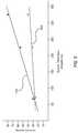
- FIG. 1Dis a graph illustrating the dependence of UC-to-UC distance on spacer thickness.
- FIG. 2is a method of forming source and drain epitaxial tips in accordance with an embodiment of the present invention.
- FIGS. 3A to 3Jillustrate structures that are formed when carrying out the method of FIG. 2 , in accordance with various embodiments of the present invention.
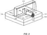
- FIG. 4shows a perspective view of a FinFET transistor architecture, configured in accordance with one embodiment of the present invention.
- FIG. 5is a graph illustrating how the UC-to-UC distance of a MOS device formed in accordance with an embodiment of the present invention is less dependent on spacer thickness.
- FIG. 6Aillustrates Schottky barrier nickel germanide (NiGe) diode measurements, confirming that the NiGe workfunction is about 85 mV of the valance band edge, in accordance with some embodiments of the present invention.
- FIG. 6Bplots simulation data that shows that such germanide materials provide a significant Rext improvement over that in conventional silicon germanium source/drain PMOS devices, in accordance with some embodiments of the present invention.
- Techniquesare disclosed for forming transistor devices having source and drain regions with high concentrations of boron doped germanium.
- the techniquescan be used, for example, to extend self-aligned epitaxial tip (SET) transistors to achieve very near to the theoretical limit of uniaxial strain. In some embodiments, this is accomplished by use of an in situ boron doped germanium provided by selective epitaxial deposition in the source and drain regions as well as their corresponding tip regions. In other embodiments, selective epitaxial deposition is used to form a bilayer construction of boron doped silicon germanium capped with a heavily boron doped germanium layer in the source/drain and respective tip regions.
- SETself-aligned epitaxial tip
- the germanium concentrationcan be, for example, in the range of 20 atomic % to 100 atomic %
- the boron concentrationcan be, for instance, in the range of 1E20 cm ⁇ 3 to 2E21 cm ⁇ 3 (e.g., germanium concentration in excess of 50 atomic % and boron concentration in excess of 2E20 cm ⁇ 3 ).
- An optional thin buffer with graded germanium and/or boron concentrationcan be used as an interfacial layer to the underlying substrate material or materials with the layer of boron doped germanium.
- a thin buffer with graded germanium and/or boron concentrationcan be used as an interfacial layer to the silicon germanium layer with the boron doped germanium cap.
- the boron doped germanium or silicon germanium layersthemselves can have a graded germanium and/or boron concentration in a similar fashion as to the optional buffers.
- boron diffusionis suppressed in germanium (the higher the concentration, the greater the suppression)
- a high concentration of boroncan be doped in the germanium, which in turn results in lower parasitic resistance and without degrading tip abruptness.
- the contact resistanceis reduced from lowering of Schottky-barrier height.
- the techniquescan be embodied, for instance, in planar or non-planar FinFET transistor devices.
- a metal oxide semiconductor (MOS) transistormay include source and drain tip regions that are designed to decrease the overall resistance of the transistor while improving short channel effects (SCE).
- these tip regionsare portions of the substrate where a dopant such as boron or carbon is implanted using an implant and diffusion technique.
- the source tip regionis formed in the area between the source region and the channel region.
- the drain tip regionis formed in the area between the drain region and the channel region. The tip regions resulting from such conventional processing minimally underdiffuse the gate dielectric layer of the transistor.
- FIG. 1Aillustrates a conventional MOS transistor 100 A formed on a substrate 102 .
- the source region 110 and the drain region 112are typically formed by either implanting dopants such as boron into the substrate or by etching the substrate and then epitaxially depositing a silicon or silicon germanium material (with a germanium concentration in the range of 10 to 40 atomic %).
- a gate stack 122is formed over a channel region 120 of the transistor 100 A.
- the gate stack 122includes a gate dielectric layer 106 and a gate electrode 104 , and spacers 108 are formed adjacent to the gate stack 122 .
- the spacers 108create a distance of about 10 to 20 nanometers (nm) between the edges of the gate dielectric layer 106 and the edges of each of the source and drain regions 110 / 112 . It is within this space that a source tip region 110 A and a drain tip region 112 A are formed. As can be seen, the implantation-diffusion based tip regions 110 A/ 112 A overlap the spacers 108 and may also overlap or underdiffuse the gate dielectric layer 106 by a distance of less than 10 nm.
- a dopantsuch as boron or carbon is implanted into the source region 110 and the drain region 112 .
- the transistor 100 Ais then annealed to cause the dopant to diffuse towards the channel region 120 .
- Angled ion implantation techniquesmay also be used to further implant dopants into those areas between the gate dielectric layer 106 and the source/drain regions 110 / 112 .
- factorssuch as the shape of the tip regions 110 A/ 112 A, the distance the dopants penetrate below the spacers 108 , and the concentration gradient of the tip regions 110 A/ 112 A are dependent on the diffusion properties of the dopant in the substrate material.
- the concentration of the tip regionswill be high proximate to the source/drain region 110 / 112 and low proximate to the channel region 120 .
- the source and drain regions 110 / 112cannot be moved closer to the channel region 120 because the dopant may again be driven into the channel region 120 . This limits how close the source and drain regions 110 / 112 can be formed to the channel region 120 , thereby constraining gate length scaling.
- FIG. 1Billustrates an example MOS device 100 B that includes source and drain epitaxial tips (generally referred to herein as epi-tips) configured in accordance with an embodiment of the present invention.
- the MOS transistor 100 Buses an undercut etch to allow the source region 110 and the drain region 112 to extend below the spacers 108 , and in some cases, below the gate dielectric layer 106 .
- the portions of the source/drain regions 110 / 112 that extend below the spacers 108 (and possibly the gate dielectric layer 106 )are referred to herein as the source epi-tip 110 B and the drain epi-tip 112 B, respectively.
- the source and drain epi-tips 110 B/ 112 Breplace the implantation/diffusion based tip regions 110 A/ 112 A described with regard to FIG. 1A .
- the source/drain regions 110 / 112 and the source/drain epi-tips 110 B/ 112 Bcan be formed, for example, by etching the substrate 102 , which includes undercutting the spacers 108 (and possibly the gate dielectric layer 106 ), and then using selective epitaxial deposition to provide an in situ boron doped germanium, or boron doped silicon germanium (SiGe) capped with heavily boron doped germanium, to fill the source/drain regions 110 / 112 and the source/drain epi-tips 110 B/ 112 B, as shown in FIG. 1B .
- the epitaxial fillmay be raised relative to the surface of substrate 102 , as further shown in FIG. 1B .
- a graded buffermay be used in one or more locations of the structure, depending on factors such as the substrate composition and extent to which misfit dislocation is to be inhibited between disparate layers of the device structure.
- the substrate 102can be a silicon substrate, or a silicon film of a silicon on insulator (SOI) substrate, or a multi-layered substrate comprising silicon, silicon germanium, germanium, and/or III-V compound semiconductors.
- SOIsilicon on insulator
- a buffercan be provided between the underlying substrate 102 and the upper boron doped germanium.
- the buffercan be a graded boron doped (or intrinsic) silicon germanium layer with the germanium composition graded from a base level concentration compatible with the underlying silicon substrate or silicon germanium substrate up to 100 atomic % (or near 100 atomic %, such as in excess of 90 atomic % or 95 atomic % or 98 atomic %).
- the germanium concentrationranges from 40 atomic % or less to in excess of 98 atomic %.
- the boron concentration within this buffercan be fixed, for example, at a high level or grade, for example, from a base concentration at or otherwise compatible with the underlying substrate up to a desired high concentration (e.g., in excess of 1E20 cm ⁇ 3 , or 5E20 cm ⁇ 3 ). Note that compatibility as used herein does not necessitate an overlap in concentration levels (for instance, the germanium concentration of the underlying substrate can be 0 to 20 atomic % and initial germanium concentration of the buffer can be 30 to 40 atomic %).
- the term ‘fixed’ with respect to a concentration levelis intended to indicate a relatively constant concentration level (e.g., the lowest concentration level in the layer is within 10% of the highest concentration level within that layer). In a more general sense, a fixed concentration level is intended to indicate the lack of an intentionally graded concentration level.
- the thickness of the buffercan vary depending on factors such as the range of concentrations being buffered, but in some embodiments is in the range of 30 to 120 Angstroms (A), such as 50 to 100 ⁇ (e.g., 60 ⁇ or 65 ⁇ ). As will be appreciated in light of this disclosure, such a graded buffer beneficially lowers the Schottky-barrier height.
- the boron doped germanium layeritself can be graded in a similar fashion.
- the boron doped germanium layercan be configured with a germanium concentration graded from a base level concentration compatible with the underlying substrate (e.g., in the range of 30 to 70 atomic %) up to 100 atomic %.
- the boron concentration within this boron doped germanium layercan range, for example, from a base concentration at or otherwise compatible with the underlying substrate up to a desired high concentration (e.g., in excess of 1E20 cm ⁇ 3 ).
- a buffercan be provided between the boron doped SiGe layer and the upper boron doped germanium cap.
- the boron doped SiGe layerhas a fixed concentration of germanium (e.g., in the range of 30 to 70 atomic %) and the buffer can be a thin SiGe layer (e.g., 30 to 120 ⁇ , such as 50 to 100 ⁇ ) having a germanium concentration graded from a base level concentration compatible with the underlying boron doped SiGe layer up to 100 atomic % (or near 100 atomic %, such as in excess of 90 atomic % or 95 atomic % or 98 atomic %).
- germaniume.g., in the range of 30 to 70 atomic %
- the buffercan be a thin SiGe layer (e.g., 30 to 120 ⁇ , such as 50 to 100 ⁇ ) having a germanium concentration graded from a base level concentration compatible with the underlying boron doped SiGe layer up to 100 atomic % (or near 100 atomic %, such as in excess of 90 atomic % or 95 atomic % or 98 atomic
- the boron concentration within this buffercan be fixed, for example, at a high level or can range, for example, from a base concentration at or otherwise compatible with the underlying SiGe layer up to a desired high concentration (e.g., in excess of 1E20 cm ⁇ 3 , 2E20 cm ⁇ 3 , 3E20 cm ⁇ 3 , 4E20 cm ⁇ 3 , or 5E20 cm ⁇ 3 ).
- the boron doped SiGe layeritself can be graded in a similar fashion.
- the boron doped SiGe layercan be configured with a germanium concentration graded from a base level concentration compatible with the underlying substrate (e.g., in the range of 30 to 70 atomic %) up to 100 atomic % (or near 100 atomic %, as previously explained).
- the boron concentration within this boron doped SiGe layercan be fixed, for example, at a high level or can range, for example, from a base concentration at or otherwise compatible with the underlying substrate up to a desired high concentration (e.g., in excess of 1E20 cm ⁇ 3 ).
- a SET architecture for planar and non-planar FinFET transistor devicesis provided.
- the devicesmay be formed in part using conventional processes such as, for example, by dummy gate oxide, thin spacer, and an isotropic undercut etch (or an ammonia etch to form faceted fin recess in monocrystalline substrate, or other suitable etch to form fin recess).
- selective epitaxial depositioncan then be used to provide in situ boron doped germanium or alternatively, a fully strained boron doped silicon germanium layer capped with heavily boron doped pure germanium, to form both tips and source/drain regions.
- Optional buffersmay be used as previously explained.
- P-type source and drain (PSD) implants or high temperature diffusion-based annealsare required, since boron is fully active as deposited.
- Any suitable high-k replacement metal gate (RMG) process flowcan also be used, where a high-k dielectric replaces the dummy gate oxide.
- Silicidation with, for example, nickel, nickel-platinum, or titanium with or without germanium pre-amorphization implantscan be used to form a low resistance germanide.
- such embodimentsextend SET transistor device architecture to achieve (near) theoretical limit of uniaxial strain.
- the source and drain epi-tips 110 B/ 112 B configured in accordance with an embodiment of the present inventioncan be formed in the same process as the source and drain regions 110 / 112 , which reduces process time.
- the lattice parameter of the source/drain epi-tips 110 B/ 112 B configured in accordance with an embodiment of the present inventioninduces a strain in the channel region 120 that increases hole mobility and therefore decreases resistance in the channel.
- Another advantage of a SET architecture configured in accordance with some embodiments of the present inventionis that the interface between the source/drain epi-tips 110 B and 112 B and the substrate material 102 that forms the channel region 120 is abrupt.
- the epitaxially deposited boron doped germanium (B:Ge) materiale.g., with B concentration in excess of 2E20 cm ⁇ 3 or 5E20 cm ⁇ 3
- the substrate material that makes up the channel region 120e.g., silicon germanium, or other suitable substrate material.
- B:Geboron doped germanium
- This structureenables the epitaxial source/drain epi-tips 110 B/ 112 B to bring the heavily boron doped high concentration germanium material in very close proximity to the channel region 120 .
- the boron in the epitaxial source/drain epi-tips 110 B/ 112 Bremains substantially or completely within the epi-tips and does not tend to diffuse into the channel region 120 .
- FIGS. 1B and 1CAnother issue with conventional methods of forming source and drain epi-tips 110 B/ 112 B concerns the effect that spacer thickness has on the undercut etch, as shown in FIGS. 1B and 1C .
- the MOS transistor 100 Bis shown having offset spacers 108 of a first thickness x 1 .
- a substrate etchhas been performed that undercuts the spacers 108 and a portion of the gate dielectric layer 106 to enable the formation of source and drain epi-tips 110 B/ 112 B.
- An undercut-to-undercut (UC-to-UC) distance 114separates source epi-tip 110 B from drain epi-tip 112 B.
- a MOS transistor 100 Cis shown with offset spacers 108 having a thickness x 2 .
- the thickness x 2is much greater than the thickness x 1 of the spacers 108 in FIG. 1B .
- the thicker spacers 108push out the undercut etch and cause the source/drain epi-tips 110 B/ 112 B to be formed further away from the channel region 120 of the transistor 100 C.
- the substrate etchtherefore undercuts less of the surface area beneath the MOS transistor 100 C.
- FIG. 1Dis a graph illustrating how spacer thickness affects the UC-to-UC distance in devices formed using known methods. The graph provides data, represented by line 118 , showing that as spacer thickness increases, the UC-to-UC distance also increases, leading to large drive current variations. Typically, for every nanometer of spacer thickness increase, the UC-to-UC distance increases by around 2 nm.
- some embodiments of the present inventionprovide methods of forming self-aligned and epitaxially deposited source and drain tips that address such issues.
- FIG. 2is a method 200 of building a MOS transistor with self-aligned source and drain epi-tips, in accordance with an embodiment of the present invention.
- FIGS. 3A through 3Jillustrate example structures that are formed as the method 200 is carried out, and in accordance with some embodiments.
- the method 200begins with providing 202 a semiconductor substrate upon which a MOS device, such as a PMOS transistor, may be formed.
- the semiconductor substratemay be implemented, for example, with a bulk silicon or a silicon-on-insulator configuration.
- the semiconductor substratemay be formed using alternate materials, which may or may not be combined with silicon, such as germanium, silicon germanium, indium antimonide, lead telluride, indium arsenide, indium phosphide, gallium arsenide, or gallium antimonide.
- any material that may serve as a foundation upon which a semiconductor device may be builtcan be used in accordance with embodiments of the present invention.
- the method 200continues with forming 204 a gate stack on the semiconductor substrate.
- the gate stackcan be formed as conventionally done or using any suitable custom techniques.
- the gate stackmay be formed by depositing and then patterning a gate dielectric layer and a gate electrode layer.
- a gate dielectric layermay be blanket deposited onto the semiconductor substrate using conventional deposition processes such as chemical vapor deposition (CVD), atomic layer deposition (ALD), spin-on deposition (SOD), or physical vapor deposition (PVD). Alternate deposition techniques may be used as well; for instance, the gate dielectric layer may be thermally grown.
- the gate dielectric materialmay be formed, for example, from materials such as silicon dioxide or high-k dielectric materials.
- high-k gate dielectric materialsinclude, for instance, hafnium oxide, hafnium silicon oxide, lanthanum oxide, lanthanum aluminum oxide, zirconium oxide, zirconium silicon oxide, tantalum oxide, titanium oxide, barium strontium titanium oxide, barium titanium oxide, strontium titanium oxide, yttrium oxide, aluminum oxide, lead scandium tantalum oxide, and lead zinc niobate.
- the high-k gate dielectric layermay be between around 5 ⁇ to around 200 ⁇ thick (e.g., 20 ⁇ to 50 ⁇ ). In general, the thickness of the gate dielectric layer should be sufficient to electrically isolate the gate electrode from the neighboring source and drain contacts.
- additional processingmay be performed on the high-k gate dielectric layer, such as an annealing process to improve the quality of the high-k material.
- a gate electrode materialmay be deposited on the gate dielectric layer using similar deposition techniques such as ALD, CVD, or PVD.
- the gate electrode materialis polysilicon or a metal layer, although other suitable gate electrode materials can be used as well.
- the gate electrode materialwhich is typically a sacrificial material that is later removed for a replacement metal gate (RMG) process, has a thickness in the range of 50 ⁇ to 500 ⁇ (e.g., 100 ⁇ ), in some example embodiments.
- a conventional patterning processmay then be carried out to etch away portions of the gate electrode layer and the gate dielectric layer to form the gate stack, as shown in FIG. 3A .
- FIG. 3Aillustrates a substrate 300 upon which a gate stack is formed.
- the gate stackincludes a gate dielectric layer 302 (which may be high-k gate dielectric material) and a sacrificial gate electrode 304 .
- the gate stackincludes a silicon dioxide gate dielectric layer 302 and a polysilicon gate electrode 304 .
- the gate stackmay also include a gate hard mask layer 306 that provides certain benefits or uses during processing, such as protecting the gate electrode 304 from subsequent ion implantation processes.
- the hard mask layer 306may be formed using typical hard mask materials, such as such as silicon dioxide, silicon nitride, and/or other conventional dielectric materials.
- the method 200continues with an ion implantation process to highly dope portions of the substrate adjacent to the gate stack, by implanting 206 dopants into the substrate.
- the dopant used in the ion implantation processcan be chosen, for example, based on its ability to increase the etch rate of the substrate material in which it is implanted, and the specific dopant selected for the ion implantation process may vary based on the substrate material(s) and the etchant used in a subsequent etching process.
- Specific dopants that may be selected to increase the etch rate of the substrateinclude, for example, carbon, phosphorous, and arsenic.
- carbonmay be used at a dosage that ranges from 1 ⁇ 10 14 to 1 ⁇ 10 16 atoms/cm 3 using an implantation energy that falls between 5 and 15 kilo-electron volts (keV).
- Phosphorousmay be used at a dosage that ranges from 1 ⁇ 10 14 to 5 ⁇ 10 15 atoms/cm 3 using an implantation energy that falls between 1 and 5 keV.
- Arsenicmay be used at a dosage that ranges from 1 ⁇ 10 14 to 5 ⁇ 10 15 atoms/cm 3 using an implantation energy that falls between 2 and 5 keV.
- Other suitable dopants and dosage schemeswill be apparent in light of this disclosure.
- the ion implantationsubstantially occurs in a vertical direction (i.e., a direction perpendicular to substrate), while in other embodiments at least a portion of the ion implantation process occurs in an angled direction to implant ions below the gate stack.
- the hard mask 306can be used to prevent doping of the gate electrode 304 material.
- the method 200continues with annealing 207 the substrate to drive the dopants further into the substrate and to reduce any damage sustained by the substrate during the ion implantation process.
- the implanting 206 and subsequent annealing 207may drive the ions to a substrate depth that falls, for example, between 2 nm and 20 nm.
- the annealing 207may be carried out at a temperature that falls, for example, between 700° C. and 1100° C. for a time duration of up sixty seconds or less (e.g., five seconds).
- the annealing temperature and durationcan vary from one embodiment to the next, depending on factors such as the diffusion rate, substrate material, dopant used, and desired end dopant concentration.
- FIG. 3Billustrates the substrate 300 after the ion implantation and diffusion process.
- the ion implantation processcreates two doped regions 308 adjacent to the gate dielectric layer 302 , for the MOS transistor being formed.
- the doped regions 308When exposed to an appropriate etchant, the doped regions 308 will have an etch rate that is higher than the etch rate of the surrounding substrate material.
- One of the doped regions 308will serve as a portion of a source region, including its self-aligned epi-tip.
- the other doped region 308will serve as a portion of a drain region, including its self-aligned epi-tip.
- portions of the doped regions 308are sited below the gate dielectric layer 302 . Note that the size of the doped regions 308 , including their depth, may vary based on the requirements of the MOS transistor being formed.
- the spacersmay be formed, for example, using conventional materials such as silicon oxide, silicon nitride, or other suitable spacer materials.
- the width of the spacersmay generally be chosen based on design requirements for the MOS transistor being formed. In accordance with some embodiments, however, the width of the spacers is not subject to design constraints imposed by the formation of the source and drain epi-tips.
- FIG. 3Cillustrates the substrate 300 with spacers 310 formed on either side of the gate electrode layer 304 and the gate dielectric layer 302 , in accordance with an example embodiment.
- the method 200continues with dry etching 210 the doped regions of the substrate to form cavities in which source/drain regions including their respective epi-tips may be formed.
- the etched cavitiesare generally adjacent to the gate stack, and the epi-tip areas are effectively extensions of the source/drain cavity regions.
- the etched cavitiesmay be formed to a depth that falls between 50 nm and 1500 nm, which can be deeper than the doped regions. In a more general sense, the etch depth can be set as needed, based on desired MOS device performance.
- the dry etch processcan use an etchant recipe that complements the dopant used in the ion implantation process to increase the etch rate of the doped regions, thereby enabling the etching process to remove substrate material from the doped regions at a faster rate than the remainder of the substrate 300 .
- thisincludes portions of the doped regions that undercut the spacers 310 and the gate dielectric layer 302 , thereby defining the self-aligned tip architecture of the transistor.
- Increasing the etch rate of the doped regionsenables the etched source and drain tip cavities to undercut the spacers 310 and the gate dielectric layer 302 without the UC-to-UC distance being substantially impacted by factors such as the thickness of the spacers, variations in the dry etch process, and other process variations.
- the dry etch processmay use a chlorinated chemistry that takes place in a plasma reactor.
- the etchant recipemay include a combination of NF 3 and Cl 2 with argon or helium used as a buffer or carrier gas.
- the flow rate for the active etchant speciesmay vary, for example, between 50 and 200 standard cubic centimeters per minute (SCCM) while the flow rate of the carrier gas may vary, for example, between 150 and 400 SCCM.
- SCCMstandard cubic centimeters per minute
- a high energy plasmamay be employed at a power that ranges, for instance, from 700 W to 1100 W with a low RF bias of less than 100 W, in accordance with some such embodiments.
- the reactor pressuremay range from around 1 pascal (Pa) to around 2 Pa, in accordance with some such embodiments.
- the etchant chemistrymay include a combination of HBr and Cl 2 .
- the flow rate for the etchant speciesmay vary, for example, between 40 SCCM and 100 SCCM.
- a high energy plasmamay be employed at a power that ranges from around 600 W to around 1000 W with a low RF bias of less than 100 W, and the reactor pressure may range from around 0.3 Pa to around 0.8 Pa, in accordance with some such embodiments.
- the etchant chemistrymay include a combination of Ar and Cl 2 .
- the flow rate for the etchant speciesmay vary, for example, between 40 SCCM and 80 SCCM.
- a medium energy plasmamay be employed at a power that ranges from around 400 W to around 800 W with a high RF bias of between around 100 W and 200 W, and the reactor pressure may range from around 1 Pa to around 2 Pa, in accordance with some such embodiments.
- the dry etch process times for each of these example embodimentsmay be, for example, up to 60 seconds per substrate, but can vary depending on factors such as desired etch depth and etchant. Such etch process parameters may vary, as will be appreciated.
- FIG. 3Dillustrates the substrate 300 after the dry etch process has been carried out, in accordance with some embodiments of the present invention.
- a source region cavity 312 and a drain region cavity 314are formed.
- a source tip cavity 312 A and a drain tip cavity 314 Ahave been formed as extensions of cavities 312 and 314 , respectively, by the etching 210 of the doped regions as previously discussed.
- the thickness of the spacers 310has minimal impact on the etching of the source tip cavity 312 A and the drain tip cavity 314 A due to the use of dopants and etchant recipes that increase the etch rate of the doped regions during etching 210 .
- wet etching 212to clean and further etch the source region cavity 312 and its source epi-tip cavity 312 A, as well as the drain region cavity 314 and its drain epi-tip cavity 314 A.
- the wet etching 212which can be carried out using conventional or custom wet etch chemistries, can be used to remove contaminants such as carbon, fluorine, chlorofluorocarbons, and oxides such as silicon oxide to provide a clean surface upon which subsequent processes may be carried out.
- the wet etching 212may also be used to remove a thin portion of the substrate along the ⁇ 111> and ⁇ 001> crystallographic planes to provide a smooth surface upon which a high quality epitaxial deposition may occur.
- the thin portion of the substrate that is etched awaymay be, for example, up to 5 nm thick and may also remove residual contaminants.
- the wet etching 212causes edges of the source region cavity 312 and its epi-tip region 312 A, as well as the drain region cavity 314 and its epi-tip region 314 A to follow the ⁇ 111> and ⁇ 001> crystallographic planes. Further note that the source and drain epi-tip regions 312 A and 314 A do not have the bulleted profile that occurs in conventional processing.
- the method 200continues with epitaxially depositing 214 in the source/drain and respective tip cavities either an in situ boron doped germanium (with an intervening thin buffer in some cases), or boron doped silicon germanium capped with a heavily boron doped germanium layer.
- This epitaxial depositionfills the source and drain cavities including their respective epi-tip regions in one process, in accordance with some embodiments.
- a CVD process or other suitable deposition techniquemay be used for the depositing 214 .
- the depositing 214may be carried out in a CVD reactor, an LPCVD reactor, or an ultra-high vacuum CVD (UHVCVD) reactor.
- the reactor temperaturemay fall, for instance, between 600° C. and 800° C. and the reactor pressure may fall, for instance, between 1 and 760 Torr.
- the carrier gasmay include, for example, hydrogen or helium at a suitable flow rate, such as between 10 and 50 SLM.
- the depositionmay be carried out using a germanium source precursor gas such as GeH 4 that is diluted in H 2 (e.g., the GeH 4 may be diluted at 1-5%).
- the diluted GeH 4may be used at a 1% concentration and at a flow rate that ranges between 50 and 300 SCCM.
- diluted B 2 H 6may be used (e.g., the B 2 H 6 may be diluted in H 2 at 1-5%).
- the diluted B 2 H 6may be used at a 3% concentration and at a flow rate that ranges between 10 and 100 SCCM.
- an etching agentmay be added to increase the selectivity of the deposition.
- HCl or Cl 2may be added at a flow rate that ranges, for example, between 50 and 300 SCCM.
- the source and drain region cavities 312 / 314 along with their respective tip regions 312 A/ 314 Aare filled with in situ boron doped germanium, thereby forming source region 318 (along with source epi-tip 318 A) and drain region 320 (along with drain epi-tip 320 A) of a MOS transistor 316 in substrate 300 .
- the boron doped germaniumhas a boron concentration in excess of 5E20 cm ⁇ 3 , such as 2E21 cm ⁇ 3 or higher.
- the thickness of the boron doped germanium deposited layermay range, for example, from 50 to 500 nm (e.g., 120 nm), in accordance with some specific embodiments, although other layer thicknesses will be apparent in light of this disclosure.
- some such embodimentsmay include a thin buffer between the pure germanium layer and the substrate. For instance, and as can further be seen in the example embodiment shown in FIG. 3F , a source buffer 313 and a drain buffer 315 are deposited prior to depositing the in situ boron doped germanium.
- the buffers 313 and 315can be a graded boron doped silicon germanium layer with the germanium composition graded from a base level concentration compatible with the underlying substrate 300 material up to 100 atomic % (or near to 100 atomic % as previously described).
- the thickness of the buffers 313 and 315will vary depending on factors such as the concentration range over which the buffer transitions and the make-up of the underlying substrate 300 . In one example embodiment having a silicon germanium substrate, the buffer thickness ranges from 2 nm to 10 nm, although other suitable thicknesses can be used also.
- the boron concentration within the buffers 313 and 315can range, for example, from a base concentration compatible with the underlying silicon germanium substrate up to a desired concentration (e.g., in excess of 1E20 cm ⁇ 3 and up to 2E21 cm ⁇ 3 ), with two specific embodiments being in excess of 2E20 cm ⁇ 3 or in excess of 5E20 cm ⁇ 3 .
- the boron concentrationcan be adjusted as necessary to provide the desired degree of conductivity, as will be appreciated in light of this disclosure.
- the source and drain region cavities 312 / 314 along with their respective tip regions 312 A/ 314 Aare filled with in situ boron doped silicon germanium to form source region 318 (along with source epi-tip 318 A) and drain region 320 (along with drain epi-tip 320 A) of MOS transistor 316 in substrate 300 .
- the boron doped silicon germanium fillis then capped with a heavily boron doped germanium layer to provide source cap 317 and drain cap 319 .
- the boron doped silicon germanium fillwhich may be epitaxially deposited in one or more layers, has a germanium concentration in the range of 30 to 70 atomic %, or higher.
- this germanium concentration of the SiGe fillmay be fixed or graded so as to increase from a base level (near substrate 300 ) to a high level (e.g., in excess of 50 atomic %, near the pure germanium cap 317 / 319 ).
- the boron concentration in some such embodimentscan be in excess of 1E20 cm ⁇ 3 , such as higher than 5E20 cm ⁇ 3 or 2E21 cm ⁇ 3 , and may also be graded so as to increase from a base level near substrate 300 to a high level (e.g., in excess of 1E20 cm ⁇ 3 or 2E20 cm ⁇ 3 or 3E20 cm ⁇ 3 , etc., near cap 317 / 319 ).
- a thin graded buffermay be used to better interface the boron doped SiGe layer with the boron doped Ge cap, as previously explained.
- the thickness of the boron doped SiGe deposited layer (or collection of layers) 318 / 320may range, for example, from 50 to 250 nm (e.g., 60 nm), and the pure germanium cap 317 / 319 may have a thickness in the range, for example, of 50 to 250 nm (e.g., 50 nm), in accordance with some specific embodiments, although alternative embodiments may have other layer and cap thicknesses, as will be apparent in light of this disclosure.
- cavitiesmay be created underneath the spacers during cyclical deposition-etch processing, and those cavities can be backfilled by an epitaxial cap layer as well (which can have, for example, the same composition as the boron doped germanium cap 317 / 319 ).
- the combination of high germanium concentration (e.g., in excess of 50 atomic % and up to pure germanium) and high boron concentration (e.g., in excess of 1E20 cm ⁇ 3 ), such as discussed with respect to embodiments shown in FIGS. 3F and 3G ,can be used to realize significantly higher conductance in the source and drain regions as well as their respective tip regions in PMOS SET transistor devices. Further, and as previously explained, since boron diffusion is sufficiently suppressed by pure germanium, no adverse SCE degradation is realized with subsequent thermal anneals despite high boron in the deposited stressor film. Barrier height lowering is also enabled from the higher concentration of germanium at the contact surface. In some example embodiments, a germanium concentration in excess of 95 atomic % and up to pure germanium (100 atomic %) can be used to achieve such benefits.
- the self-aligned source and drain epi-tips of the MOS transistor 316have an abrupt boundary.
- the interface between the source/drain epi-tips and the channel regionis clear and well-defined.
- the heavily boron doped germanium layerlayer 318 / 320 of FIG. 3F or cap 317 / 319 of FIG. 3G
- the substrate 300 materialthat makes up the channel region.
- the boron in the source/drain epi-tips 318 A/ 320 Aremains substantially or completely within the epi-tips and does not tend to diffuse into the channel region, thereby enabling the heavily boron doped germanium material in very close proximity to the channel region relative to conventional techniques.
- the source/drain epi-tips 318 A/ 320 Amay undercut the gate dielectric layer 302 by more than 10 nm. This in turn enables the gate length to be scaled down without having to shorten the channel region.
- Forming the source and drain epi-tips in relatively close proximity to the channel regionalso imparts a larger hydrostatic stress on the channel. This stress increases the strain within the channel, thereby increasing mobility in the channel and increasing drive current. This stress can be further amplified by increasing the germanium concentration of the source and drain epi-tips. This is an improvement over diffusion-based processes where the tip regions generally do not induce a strain on the channel region.
- MOS transistor 316various conventional MOS processing can be carried out to complete fabrication of MOS transistor 316 , such as replacement gate oxide processes, replacement metal gate processes, annealing, and salicidation processes, that may further modify the transistor 316 and/or provide the necessary electrical interconnections.
- the method 200may continue with depositing 216 an interlayer dielectric (ILD) over the transistor 316 , and then planarizing the ILD layer as commonly done.
- ILDinterlayer dielectric
- the ILD layermay be formed using materials known for the applicability in dielectric layers for integrated circuit structures, such as low-k dielectric materials.
- Such dielectric materialsinclude, for example, oxides such as silicon dioxide (SiO 2 ) and carbon doped oxide (CDO), silicon nitride, organic polymers such as perfluorocyclobutane or polytetrafluoroethylene, fluorosilicate glass (FSG), and organosilicates such as silsesquioxane, siloxane, or organosilicate glass.
- the ILD layermay include pores or other voids to further reduce its dielectric constant.
- FIG. 3Hillustrates an example ILD layer 322 that has been deposited and then planarized down to the hard mask 306 .
- the method 200continues with removing 218 the gate stack (including the high-k gate dielectric layer 302 , the sacrificial gate electrode 304 , and the hard mask layer 306 ) using an etching process as conventionally done. In alternate implementations, only the sacrificial gate 304 is removed.
- FIG. 3Iillustrates the trench opening that is formed when the gate stack is etched away, in accordance with one such embodiment. If the gate dielectric layer is removed, the method may continue with depositing 220 a new gate dielectric layer into the trench opening. Any suitable high-k dielectric materials such as those previously described may be used here, such as hafnium oxide. The same deposition processes may also be used.
- Replacement of the gate dielectric layermay be used, for example, to address any damage that may have occurred to the original gate dielectric layer during application of the dry and wet etch processes, and/or to replace a low-k or sacrificial dielectric material with a high-k or otherwise desired gate dielectric material.
- the method 200may then continue with depositing 222 the metal gate electrode layer into the trench and over the gate dielectric layer.
- Conventional metal deposition processesmay be used to form the metal gate electrode layer, such as CVD, ALD, PVD, electroless plating, or electroplating.
- the metal gate electrode layermay include, for example, a P-type workfunction metal, such as ruthenium, palladium, platinum, cobalt, nickel, and conductive metal oxides e.g., ruthenium oxide).
- two or more metal gate electrode layersmay be deposited.
- a workfunction metalmay be deposited followed by a suitable metal gate electrode fill metal such as aluminum.
- FIG. 3Jillustrates an example high-k gate dielectric layer 324 and a metal gate electrode 326 that have been deposited into the trench opening, in accordance with one embodiment.
- Metalization of the source and drain contactscan be carried out using a silicidation process (generally, deposition of contact metal and subsequent annealing). For instance, silicidation with nickel, aluminum, nickel-platinum or nickel-aluminum or other alloys of nickel and aluminum, or titanium with or without germanium pre-amorphization implants can be used to form a low resistance germanide.
- the boron doped germanium epi layerallows for metal-germanide formation (e.g., nickel-germanium).
- the germanideallows for significantly lower Schottky-barrier height and improved contact resistance (including Rext) over that in conventional metal-silicide systems.
- conventional transistorstypically use a source/drain SiGe epi process, with germanium concentration in the range of 30-40 atomic %.
- Such conventional systemsexhibit Rext values of about 140 Ohm*um, limited by epi/silicide interfacial resistance, which is high and may impede future gate pitch scaling.
- Some embodiments of the present inventionallow for a significant improvement in Rext in PMOS devices (e.g., about a 2 ⁇ improvement, or a Rext of about 70 Ohm*um), which can better support PMOS device scaling.
- transistors having a source/drain configured with heavily boron doped germanium in accordance with an embodiment of the presentwith a boron concentration in excess of 1E20 cm ⁇ 3 and a germanium concentration in excess of 50 atomic % and up to or otherwise near pure germanium (100 atomic %) at the interface between the source/drain epi-tips and the channel region, can exhibit Rext values of less than 100 Ohm*um, and in some cases less than 90 Ohm*um, and in some cases less than 80 Ohm*um, and in some cases less than 75 Ohm*um, or lower.
- the source and drain epi-tipshave been disclosed that reduce the overall resistance of the MOS transistor and increase channel strain due to increased boron doped germanium volume (e.g., boron doped germanium or boron doped silicon germanium volume with a germanium cap).
- the source and drain epi-tipsdo not have a bulleted profile, form an abrupt boundary between the channel region and the source and drain regions, and/or have a doping concentration that is more readily controlled, yielding a more optimized source-drain profile.
- the source and drain epi-tipscan be etched without being substantially impacted by the spacer thickness. This self-aligned process can therefore be used to increase performance while minimizing process variation, where desirable to do so.
- FinFETis a transistor built around a thin strip of semiconductor material (generally referred to as the fin).
- the transistorincludes the standard field effect transistor (FET) nodes, including a gate, a gate dielectric, a source region, and a drain region.
- the conductive channel of the deviceresides on the outer sides of the fin beneath the gate dielectric. Specifically, current runs along both sidewalls of the fin (sides perpendicular to the substrate surface) as well as along the top of the fin (side parallel to the substrate surface). Because the conductive channel of such configurations essentially resides along the three different outer, planar regions of the fin, such a FinFET design is sometimes referred to as a tri-gate FinFET.
- Other types of FinFET configurationsare also available, such as so-called double-gate FinFETs, in which the conductive channel principally resides only along the two sidewalls of the fin (and not along the top of the fin).
- FIG. 4shows a perspective view of an example tri-gate architecture, configured in accordance with one embodiment of the present invention.
- the tri-gate deviceincludes a substrate 400 having a semiconductor body or fin 260 (represented by dashed lines) extending from the substrate 400 through isolation regions 710 , 720 .
- a gate electrode 340is formed over 3 surfaces of the fin 260 to form 3 gates.
- a hard mask 410is formed on top of the gate electrode 340 .
- Gate spacers 460 , 470are formed at opposite sidewalls of the gate electrode 340 .
- a source regioncomprises the epitaxial region 531 formed on a recessed source interface 266 and on one fin 260 sidewall
- a drain regioncomprises the epitaxial region 531 formed on a recessed source interface 266 and on the opposing fin 260 sidewall (not shown).
- a cap layer 541is deposited over the epitaxial regions 531 .
- the isolation regions 710 , 720are shallow trench isolation (STI) regions formed by common techniques, such as etching the substrate 200 to form trenches, and then depositing oxide material onto the trenches to form the STI regions.
- the isolation regions 710 , 720can be made from any well known insulative material, such as SiO 2 .
- substrate 400may be a silicon substrate, or SOI substrate, or a multi-layered substrate).
- the bilayer structure of the epitaxial region 531 and cap layer 541can be implemented using an in situ boron doped silicon germanium capped with a heavily boron doped germanium, with an optional germanium and/or boron graded buffer between the two bilayers.
- a buffermay be used to transition from a base level germanium/boron concentration compatible with the boron doped SiGe deposited for epitaxial region 531 in the recessed source interface 266 to the heavily boron doped germanium cap 541 .
- germanium and/or boron concentration gradingcan be implemented directly in the epitaxial region 531 , rather than in an intervening graded buffer arrangement.
- germanium and/or boron concentration gradingcan be implemented directly in the epitaxial region 531 , rather than in an intervening graded buffer arrangement.
- an alternative to the tri-gate configurationis a double-gate architecture, which includes a dielectric/isolation layer on top of the fin 260 .
- FIG. 5is a graph illustrating an improvement made available by using self-aligned source and drain epi-tips configured in accordance with one example embodiment of the present invention.
- Line 500represents data collected for MOS devices built using techniques provided herein. As shown, the UC-to-UC distance is much less impacted by spacer thickness than devices formed using conventional processes, the data for which is again represented by line 118 .
- FIGS. 6A and 6Bfurther demonstrate improvements enabled by using self-aligned source and drain epi-tips configured in accordance with one example embodiment of the present invention.
- FIG. 6Aillustrates Schottky barrier NiGe diode measurements (leakage v.
- FIG. 6Bplots simulation data that shows that such germanide materials and Schottky barrier height improvement enables more than a 2 ⁇ Rext improvement over that in conventional SiGe source/drain PMOS devices, in accordance with some example embodiments of the present invention.
- the Schottky barrier heightis the rectifying barrier for electrical conduction across a semiconductor-metal junction.
- the magnitude of the Schottky barrier heightreflects a mismatch in the energy position of the metal's Fermi level and the majority carrier band edge of the semiconductor across the semiconductor-metal interface.
- the Schottky barrier heightis the difference between the metal Fermi level and the valence band maximum of the semiconductor.
- various embodiments of the present invention provided hereincan be used to address several transistor scaling issues, such as providing for higher channel mobility with pitch and power supply (Vcc) scaling, providing reduced source/drain and contact resistance, providing for improved channel abruptness, and providing reduced barrier height between salicide and source/drain to minimize overall parasitic resistance, particularly in planar and non-planar architectures. Numerous embodiments will be apparent in light of this disclosure.
- Vccpitch and power supply
- the deviceincludes a substrate having a channel region.
- the devicefurther includes a gate electrode above the channel region, wherein a gate dielectric layer is provided between the gate electrode and the channel region and spacers are provided on sides of the gate electrode.
- the devicefurther includes source and drain regions formed in the substrate and adjacent to the channel region, each of the source and drain regions including a tip region that extends under the gate dielectric layer and/or a corresponding one of the spacers, wherein the source and drain regions comprise a boron doped germanium layer having a germanium concentration in excess of 50 atomic % and a boron concentration in excess of 1E20 cm ⁇ 3 .
- the deviceis one of a planar or FinFET PMOS transistor.
- the devicemay include metal-germanide source and drain contacts.
- the devicemay include an interlayer dielectric over the source and drain regions.
- the devicemay include a buffer between the substrate and the boron doped germanium layer.
- the bufferhas a germanium concentration that is graded from a base level concentration compatible with the substrate to a high concentration in excess of 95 atomic %.
- the bufferhas a boron concentration that is graded from a base level concentration compatible with the substrate to a high concentration in excess of 1E20 cm ⁇ 3 .
- the boron doped germanium layerhas a bilayer construction comprising a boron doped silicon germanium portion and a boron doped germanium cap thereon.
- the boron doped silicon germanium portionhas a germanium concentration that is graded from a base level concentration compatible with the substrate to a high concentration in excess of 50 atomic %
- the boron doped germanium caphas a germanium concentration in excess of 95 atomic %.
- the boron doped silicon germanium portionhas a boron concentration that is graded from a base level concentration compatible with the substrate to a high concentration in excess of 1E20 cm ⁇ 3 .
- the boron doped silicon germanium portionhas a fixed germanium concentration
- the devicefurther comprises a buffer between the boron doped silicon germanium portion and the boron doped germanium cap, the buffer having a germanium concentration that is graded from a base level concentration compatible with the boron doped silicon germanium portion to a high concentration in excess of 50 atomic %, and a boron concentration that is graded from a base level concentration compatible with the boron doped silicon germanium portion to a high concentration in excess of 1E20 cm ⁇ 3 .
- the boron concentrationcan be set higher based on factors such as desired conductivity, and in some such example cases is in excess of 2E20 cm ⁇ 3 or 3E20 cm ⁇ 3 or 4E20 cm ⁇ 3 or 5E20 cm ⁇ 3 2E21 cm ⁇ 3 .
- the deviceincludes a substrate having a channel region and a gate electrode above the channel region, wherein a gate dielectric layer is provided between the gate electrode and the channel region and spacers are provided on sides of the gate electrode.
- the devicefurther includes source and drain regions formed in the substrate and adjacent to the channel region, each of the source and drain regions including a tip region that extends under the gate dielectric layer and/or a corresponding one of the spacers, wherein the source and drain regions comprise a boron doped germanium layer having a germanium concentration in excess of 50 atomic % and a boron concentration in excess of 2E20 cm ⁇ 3 .
- the devicefurther includes metal-germanide source and drain contacts.
- the devicemay further include a buffer between the substrate and the boron doped germanium layer, wherein the buffer has a germanium concentration that is graded from a base level concentration compatible with the substrate to a high concentration in excess of 95 atomic %, and a boron concentration that is graded from a base level concentration compatible with the substrate to a high concentration in excess of 2E20 cm ⁇ 3 .
- the boron doped germanium layerhas a bilayer construction comprising a boron doped silicon germanium portion and a boron doped germanium cap thereon.
- the boron doped silicon germanium portionhas a germanium concentration that is graded from a base level concentration compatible with the substrate to a high concentration in excess of 50 atomic %, and the boron doped germanium cap has a germanium concentration in excess of 95 atomic %. In some such specific embodiments, the boron doped silicon germanium portion has a boron concentration that is graded from a base level concentration compatible with the substrate to a high concentration in excess of 2E20 cm ⁇ 3 .
- the boron doped silicon germanium portionhas a fixed germanium concentration
- the devicefurther comprises a thin buffer between the boron doped silicon germanium portion and the boron doped germanium cap, the buffer having a germanium concentration that is graded from a base level concentration compatible with the boron doped silicon germanium portion to a high concentration in excess of 50 atomic %, and a boron concentration that is graded from a base level concentration compatible with the boron doped silicon germanium portion to a high concentration in excess of 2E20 cm ⁇ 3 , the buffer having a thickness of less than 100 Angstroms.
- Another embodiment of the present inventionprovides a method for forming a transistor device.
- the methodincludes providing a substrate having a channel region, and providing a gate electrode above the channel region, wherein a gate dielectric layer is provided between the gate electrode and the channel region and spacers are provided on sides of the gate electrode.
- the methodcontinues with forming source and drain regions in the substrate and adjacent to the channel region, each of the source and drain regions including a tip region that extends under the gate dielectric layer and/or a corresponding one of the spacers, wherein the source and drain regions comprise a boron doped germanium layer having a germanium concentration in excess of 50 atomic % and a boron concentration in excess of 1E20 cm ⁇ 3 .
- the methodfurther includes providing a buffer between the substrate and the boron doped germanium layer, wherein the buffer has a germanium concentration that is graded from a base level concentration compatible with the substrate to a high concentration in excess of 95 atomic %, and a boron concentration that is graded from a base level concentration compatible with the substrate to a high concentration in excess of 1E20 cm ⁇ 3 .
- the boron doped germanium layerhas a bilayer construction comprising a boron doped silicon germanium portion and a boron doped germanium cap thereon.
- the boron doped silicon germanium portionhas a germanium concentration that is graded from a base level concentration compatible with the substrate to a high concentration in excess of 50 atomic %, and the boron doped germanium cap has a germanium concentration in excess of 95 atomic %.
- the boron doped silicon germanium portionhas a fixed germanium concentration
- the methodfurther includes providing a buffer between the boron doped silicon germanium portion and the boron doped germanium cap, the buffer having a germanium concentration that is graded from a base level concentration compatible with the boron doped silicon germanium portion to a high concentration in excess of 50 atomic %, and a boron concentration that is graded from a base level concentration compatible with the boron doped silicon germanium portion to a high concentration in excess of 1E20 cm ⁇ 3.
- the boron doped silicon germanium portionhas a boron concentration that is graded from a base level concentration compatible with the substrate to a high concentration in excess of 1E20 cm ⁇ 3 .
- some embodimentsmay include source and drain regions fabricated as described herein (e.g., having a germanium concentration in excess of 50 atomic % and a boron concentration in excess of 1E20 cm ⁇ 3 ), but still use conventional processing (e.g., implantation and annealing) to form the tips of the source and drain regions.
- the tipsmay have a lower germanium and/or boron concentration than the main source/drain region, which may be acceptable in some applications.
- only tips of the source and drain regionsmay be configured with the high germanium and boron concentrations and the main portions of the source and drain regions may have conventional or otherwise lower germanium/boron concentrations. It is intended that the scope of the invention be limited not by this detailed description, but rather by the claims appended hereto.
Landscapes
- Engineering & Computer Science (AREA)
- Physics & Mathematics (AREA)
- Condensed Matter Physics & Semiconductors (AREA)
- General Physics & Mathematics (AREA)
- Computer Hardware Design (AREA)
- Microelectronics & Electronic Packaging (AREA)
- Power Engineering (AREA)
- Manufacturing & Machinery (AREA)
- Insulated Gate Type Field-Effect Transistor (AREA)
- Chemical & Material Sciences (AREA)
- Crystallography & Structural Chemistry (AREA)
- Composite Materials (AREA)
- Materials Engineering (AREA)
- Electrodes Of Semiconductors (AREA)
- Thin Film Transistor (AREA)
- Metal-Oxide And Bipolar Metal-Oxide Semiconductor Integrated Circuits (AREA)
- Recrystallisation Techniques (AREA)
Abstract
Description
Claims (25)
Priority Applications (68)
| Application Number | Priority Date | Filing Date | Title |
|---|---|---|---|
| US12/975,278US8901537B2 (en) | 2010-12-21 | 2010-12-21 | Transistors with high concentration of boron doped germanium |
| KR1020157012018AKR101691115B1 (en) | 2010-12-21 | 2011-09-30 | Selective germanium p-contact metalization through trench |
| JP2013546135AJP5732142B2 (en) | 2010-12-21 | 2011-09-30 | Selective germanium P-contact metallization through trenches |
| US13/990,238US9117791B2 (en) | 2010-12-21 | 2011-09-30 | Selective germanium P-contact metalization through trench |
| PCT/US2011/054198WO2012087403A1 (en) | 2010-12-21 | 2011-09-30 | Contact resistance reduction employing germanium overlayer pre-contact metalization |
| EP11850136.0AEP2656389B1 (en) | 2010-12-21 | 2011-09-30 | Cmos integrated circuit device having selective germanium p-contact metallization through trench |
| EP19188924.5AEP3582265A1 (en) | 2010-12-21 | 2011-09-30 | Contact resistance reduction employing germanium overlayer pre-contact metalization |
| SG2013043252ASG190998A1 (en) | 2010-12-21 | 2011-09-30 | Selective germanium p-contact metalization through trench |
| EP11852027.9AEP2656393B1 (en) | 2010-12-21 | 2011-09-30 | Contact resistance reduction employing germanium overlayer pre-contact metalization |
| KR1020197004261AKR102079356B1 (en) | 2010-12-21 | 2011-09-30 | Selective germanium p-contact metalization through trench |
| KR1020167036162AKR101784226B1 (en) | 2010-12-21 | 2011-09-30 | Transistor device, semiconductor device, and method for forming transistor device with selective germanium p-contact metallization through trench |
| CN201180061440.2ACN103329274B (en) | 2010-12-21 | 2011-09-30 | Selective Ge P-Contact Metallization Through Trench |
| KR1020137016072AKR101489611B1 (en) | 2010-12-21 | 2011-09-30 | Contact resistance reduction employing germanium overlayer pre-contact metalization |
| KR1020207016569AKR102168550B1 (en) | 2010-12-21 | 2011-09-30 | Selective germanium p-contact metalization through trench |
| JP2013546134AJP5714721B2 (en) | 2010-12-21 | 2011-09-30 | Contact resistance reduction using germanium overlayer pre-contact metallization |
| CN201610313170.4ACN105826390B (en) | 2010-12-21 | 2011-09-30 | Transistor device, electronic device, and method of forming a transistor device |
| PCT/US2011/054202WO2012087404A1 (en) | 2010-12-21 | 2011-09-30 | Selective germanium p-contact metalization through trench |
| KR1020137016008AKR20130088179A (en) | 2010-12-21 | 2011-09-30 | Selective germanium p-contact metalization through trench |
| CN201180062116.2ACN103270598B (en) | 2010-12-21 | 2011-09-30 | Transistor device, electronic device, and method of forming a transistor device |
| EP17193291.6AEP3312886A1 (en) | 2010-12-21 | 2011-09-30 | Selective germanium p-contact metalization through trench |
| CN201610088996.5ACN105720091B (en) | 2010-12-21 | 2011-09-30 | Across the selective germanium P contact metallization of groove |
| KR1020177027385AKR101949894B1 (en) | 2010-12-21 | 2011-09-30 | Selective germanium p-contact metalization through trench |
| SG2013043310ASG191003A1 (en) | 2010-12-21 | 2011-09-30 | Contact resistance reduction employing germanium overlayer pre-contact metalization |
| KR1020207004353AKR102123036B1 (en) | 2010-12-21 | 2011-09-30 | Selective germanium p-contact metalization through trench |
| KR1020137016371AKR101510029B1 (en) | 2010-12-21 | 2011-12-07 | Transistors with high concentration of boron doped germanium |
| SG2013043336ASG191005A1 (en) | 2010-12-21 | 2011-12-07 | Transistors with high concentration of boron doped germanium |
| EP11851579.0AEP2656392A4 (en) | 2010-12-21 | 2011-12-07 | HIGH CONCENTRATION TRANSISTORS IN GERMANIUM DOPED BY BORON |
| EP19191370.6AEP3588579A1 (en) | 2010-12-21 | 2011-12-07 | Transistors with high concentration of boron doped germanium |
| CN201180062124.7ACN103270599B (en) | 2010-12-21 | 2011-12-07 | Transistors with a high concentration of boron-doped germanium |
| CN201610552470.8ACN106684148B (en) | 2010-12-21 | 2011-12-07 | Transistor with high concentration of boron-doped germanium |
| JP2013543323AJP2014504453A (en) | 2010-12-21 | 2011-12-07 | Transistor with high boron-doped germanium concentration |
| PCT/US2011/063813WO2012087581A2 (en) | 2010-12-21 | 2011-12-07 | Transistors with high concentration of boron doped germanium |
| TW100145538ATWI544630B (en) | 2010-12-21 | 2011-12-09 | A transistor with a high concentration of boron-doped germanium |
| KR1020137015944AKR20130111592A (en) | 2010-12-21 | 2011-12-20 | Column IV Transistors for PMOS Integration |
| PCT/US2011/066129WO2012088097A2 (en) | 2010-12-21 | 2011-12-20 | Column iv transistors for pmos integration |
| KR1020177036360AKR101978085B1 (en) | 2010-12-21 | 2011-12-20 | Column iv transistors for pmos integration |
| CN201610340122.4ACN105932063B (en) | 2010-12-21 | 2011-12-20 | Group IV transistors for PMOS integration |
| JP2013546324AJP5714722B2 (en) | 2010-12-21 | 2011-12-20 | Transistor device, integrated circuit, and manufacturing method |
| EP18164957.5AEP3361512B1 (en) | 2010-12-21 | 2011-12-20 | Column iv transistors for pmos integration |
| SG2013043328ASG191004A1 (en) | 2010-12-21 | 2011-12-20 | Column iv transistors for pmos integration |
| PL18164957TPL3361512T3 (en) | 2010-12-21 | 2011-12-20 | Column IV transistors for PMOS integration |
| EP11850350.7AEP2656391B1 (en) | 2010-12-21 | 2011-12-20 | Column iv transistors for pmos integration |
| KR1020157012262AKR101812389B1 (en) | 2010-12-21 | 2011-12-20 | Column iv transistors for pmos integration |
| CN201180062107.3ACN103270597B (en) | 2010-12-21 | 2011-12-20 | Group IV Transistors for PMOS Integration |
| EP20177754.7AEP3726588A1 (en) | 2010-12-21 | 2011-12-20 | Column iv transistors for pmos integration |
| US13/990,249US9437691B2 (en) | 2010-12-21 | 2011-12-20 | Column IV transistors for PMOS integration |
| TW108107651ATWI756520B (en) | 2010-12-21 | 2012-12-18 | Column iv transistors for pmos integration |
| TW107102233ATWI690084B (en) | 2010-12-21 | 2012-12-18 | Group IV transistors for PMOS integration |
| TW105122618ATWI643342B (en) | 2010-12-21 | 2012-12-18 | Column iv transistors for pmos integration |
| US14/535,387US9627384B2 (en) | 2010-12-21 | 2014-11-07 | Transistors with high concentration of boron doped germanium |
| US14/673,143US9484432B2 (en) | 2010-12-21 | 2015-03-30 | Contact resistance reduction employing germanium overlayer pre-contact metalization |
| US14/807,285US9349810B2 (en) | 2010-12-21 | 2015-07-23 | Selective germanium P-contact metalization through trench |
| US15/162,551US9722023B2 (en) | 2010-12-21 | 2016-05-23 | Selective germanium P-contact metalization through trench |
| US15/255,902US10090383B2 (en) | 2010-12-21 | 2016-09-02 | Column IV transistors for PMOS integration |
| US15/339,308US10297670B2 (en) | 2010-12-21 | 2016-10-31 | Contact resistance reduction employing germanium overlayer pre-contact metalization |
| JP2017064009AJP6329294B2 (en) | 2010-12-21 | 2017-03-28 | Transistor with high boron-doped germanium concentration |
| US15/489,569US20170221724A1 (en) | 2010-12-21 | 2017-04-17 | Transistors with high concentration of boron doped germanium |
| US15/640,966US10304927B2 (en) | 2010-12-21 | 2017-07-03 | Selective germanium p-contact metalization through trench |
| JP2018080942AJP2018113484A (en) | 2010-12-21 | 2018-04-19 | Transistor with high boron-doped germanium concentration |
| US16/037,728US10811496B2 (en) | 2010-12-21 | 2018-07-17 | Transistor devices having source/drain structure configured with high germanium content portion |
| US16/402,739US10553680B2 (en) | 2010-12-21 | 2019-05-03 | Selective germanium P-contact metalization through trench |
| US16/416,445US10700178B2 (en) | 2010-12-21 | 2019-05-20 | Contact resistance reduction employing germanium overlayer pre-contact metalization |
| JP2019189786AJP2020074389A (en) | 2010-12-21 | 2019-10-16 | Transistor with high boron-doped germanium concentration |
| US16/707,490US11387320B2 (en) | 2010-12-21 | 2019-12-09 | Transistors with high concentration of germanium |
| US16/722,855US10879353B2 (en) | 2010-12-21 | 2019-12-20 | Selective germanium P-contact metalization through trench |
| US16/881,541US11251281B2 (en) | 2010-12-21 | 2020-05-22 | Contact resistance reduction employing germanium overlayer pre-contact metalization |
| US17/025,077US11508813B2 (en) | 2010-12-21 | 2020-09-18 | Column IV transistors for PMOS integration |
| US17/667,821US20220271125A1 (en) | 2010-12-21 | 2022-02-09 | Transistor devices having source/drain structure configured with high germanium content portion |
Applications Claiming Priority (1)
| Application Number | Priority Date | Filing Date | Title |
|---|---|---|---|
| US12/975,278US8901537B2 (en) | 2010-12-21 | 2010-12-21 | Transistors with high concentration of boron doped germanium |
Related Child Applications (10)
| Application Number | Title | Priority Date | Filing Date |
|---|---|---|---|
| US13/990,224Continuation-In-PartUS8994104B2 (en) | 1999-09-28 | 2011-09-30 | Contact resistance reduction employing germanium overlayer pre-contact metalization |
| PCT/US2011/054202Continuation-In-PartWO2012087404A1 (en) | 2010-12-21 | 2011-09-30 | Selective germanium p-contact metalization through trench |
| PCT/US2011/054202ContinuationWO2012087404A1 (en) | 2010-12-21 | 2011-09-30 | Selective germanium p-contact metalization through trench |
| US13/990,238Continuation-In-PartUS9117791B2 (en) | 2010-12-21 | 2011-09-30 | Selective germanium P-contact metalization through trench |
| US13/990,238ContinuationUS9117791B2 (en) | 2010-12-21 | 2011-09-30 | Selective germanium P-contact metalization through trench |
| PCT/US2011/054198Continuation-In-PartWO2012087403A1 (en) | 1999-09-28 | 2011-09-30 | Contact resistance reduction employing germanium overlayer pre-contact metalization |
| US13/990,249Continuation-In-PartUS9437691B2 (en) | 2010-12-21 | 2011-12-20 | Column IV transistors for PMOS integration |
| US13/990,249ContinuationUS9437691B2 (en) | 2010-12-21 | 2011-12-20 | Column IV transistors for PMOS integration |
| PCT/US2011/066129Continuation-In-PartWO2012088097A2 (en) | 2010-12-21 | 2011-12-20 | Column iv transistors for pmos integration |
| US14/535,387ContinuationUS9627384B2 (en) | 2010-12-21 | 2014-11-07 | Transistors with high concentration of boron doped germanium |
Publications (2)
| Publication Number | Publication Date |
|---|---|
| US20120153387A1 US20120153387A1 (en) | 2012-06-21 |
| US8901537B2true US8901537B2 (en) | 2014-12-02 |
Family
ID=46233263
Family Applications (16)
| Application Number | Title | Priority Date | Filing Date |
|---|---|---|---|
| US12/975,278Active2032-09-01US8901537B2 (en) | 2010-12-21 | 2010-12-21 | Transistors with high concentration of boron doped germanium |
| US13/990,238Active2031-03-22US9117791B2 (en) | 2010-12-21 | 2011-09-30 | Selective germanium P-contact metalization through trench |
| US13/990,249Active2031-09-11US9437691B2 (en) | 2010-12-21 | 2011-12-20 | Column IV transistors for PMOS integration |
| US14/535,387Active2031-04-05US9627384B2 (en) | 2010-12-21 | 2014-11-07 | Transistors with high concentration of boron doped germanium |
| US14/807,285ActiveUS9349810B2 (en) | 2010-12-21 | 2015-07-23 | Selective germanium P-contact metalization through trench |
| US15/162,551ActiveUS9722023B2 (en) | 2010-12-21 | 2016-05-23 | Selective germanium P-contact metalization through trench |
| US15/255,902ActiveUS10090383B2 (en) | 2010-12-21 | 2016-09-02 | Column IV transistors for PMOS integration |
| US15/489,569AbandonedUS20170221724A1 (en) | 2010-12-21 | 2017-04-17 | Transistors with high concentration of boron doped germanium |
| US15/640,966Active2031-04-28US10304927B2 (en) | 2010-12-21 | 2017-07-03 | Selective germanium p-contact metalization through trench |
| US16/037,728Active2031-03-08US10811496B2 (en) | 2010-12-21 | 2018-07-17 | Transistor devices having source/drain structure configured with high germanium content portion |
| US16/402,739ActiveUS10553680B2 (en) | 2010-12-21 | 2019-05-03 | Selective germanium P-contact metalization through trench |
| US16/707,490Active2031-09-28US11387320B2 (en) | 2010-12-21 | 2019-12-09 | Transistors with high concentration of germanium |
| US16/722,855ActiveUS10879353B2 (en) | 2010-12-21 | 2019-12-20 | Selective germanium P-contact metalization through trench |
| US16/881,541ActiveUS11251281B2 (en) | 2010-12-21 | 2020-05-22 | Contact resistance reduction employing germanium overlayer pre-contact metalization |
| US17/025,077Active2031-01-17US11508813B2 (en) | 2010-12-21 | 2020-09-18 | Column IV transistors for PMOS integration |
| US17/667,821AbandonedUS20220271125A1 (en) | 2010-12-21 | 2022-02-09 | Transistor devices having source/drain structure configured with high germanium content portion |
Family Applications After (15)
| Application Number | Title | Priority Date | Filing Date |
|---|---|---|---|
| US13/990,238Active2031-03-22US9117791B2 (en) | 2010-12-21 | 2011-09-30 | Selective germanium P-contact metalization through trench |
| US13/990,249Active2031-09-11US9437691B2 (en) | 2010-12-21 | 2011-12-20 | Column IV transistors for PMOS integration |
| US14/535,387Active2031-04-05US9627384B2 (en) | 2010-12-21 | 2014-11-07 | Transistors with high concentration of boron doped germanium |
| US14/807,285ActiveUS9349810B2 (en) | 2010-12-21 | 2015-07-23 | Selective germanium P-contact metalization through trench |
| US15/162,551ActiveUS9722023B2 (en) | 2010-12-21 | 2016-05-23 | Selective germanium P-contact metalization through trench |
| US15/255,902ActiveUS10090383B2 (en) | 2010-12-21 | 2016-09-02 | Column IV transistors for PMOS integration |
| US15/489,569AbandonedUS20170221724A1 (en) | 2010-12-21 | 2017-04-17 | Transistors with high concentration of boron doped germanium |
| US15/640,966Active2031-04-28US10304927B2 (en) | 2010-12-21 | 2017-07-03 | Selective germanium p-contact metalization through trench |
| US16/037,728Active2031-03-08US10811496B2 (en) | 2010-12-21 | 2018-07-17 | Transistor devices having source/drain structure configured with high germanium content portion |
| US16/402,739ActiveUS10553680B2 (en) | 2010-12-21 | 2019-05-03 | Selective germanium P-contact metalization through trench |
| US16/707,490Active2031-09-28US11387320B2 (en) | 2010-12-21 | 2019-12-09 | Transistors with high concentration of germanium |
| US16/722,855ActiveUS10879353B2 (en) | 2010-12-21 | 2019-12-20 | Selective germanium P-contact metalization through trench |
| US16/881,541ActiveUS11251281B2 (en) | 2010-12-21 | 2020-05-22 | Contact resistance reduction employing germanium overlayer pre-contact metalization |
| US17/025,077Active2031-01-17US11508813B2 (en) | 2010-12-21 | 2020-09-18 | Column IV transistors for PMOS integration |
| US17/667,821AbandonedUS20220271125A1 (en) | 2010-12-21 | 2022-02-09 | Transistor devices having source/drain structure configured with high germanium content portion |
Country Status (9)
| Country | Link |
|---|---|
| US (16) | US8901537B2 (en) |
| EP (9) | EP2656393B1 (en) |
| JP (7) | JP5732142B2 (en) |
| KR (12) | KR101784226B1 (en) |
| CN (8) | CN105826390B (en) |
| PL (1) | PL3361512T3 (en) |
| SG (4) | SG191003A1 (en) |
| TW (4) | TWI544630B (en) |
| WO (4) | WO2012087404A1 (en) |
Cited By (27)
| Publication number | Priority date | Publication date | Assignee | Title |
|---|---|---|---|---|
| US20150155359A1 (en)* | 2012-11-08 | 2015-06-04 | Taiwan Semiconductor Manufacturing Company, Ltd. | Contact Structure of Semiconductor Device |
| US20150270399A1 (en)* | 2012-11-06 | 2015-09-24 | Institute of Microelectronics, Chinese Academy of Sciences | Semiconductor structure and method for manufacturing the same |
| US20150325647A1 (en)* | 2011-05-16 | 2015-11-12 | Narasimhulu Kanike | INTEGRATED CIRCUIT (IC) CHIP HAVING BOTH METAL AND SILICON GATE FIELD EFFECT TRANSISTORs (FETs) AND METHOD OF MANUFACTURE |
| US9287138B2 (en) | 2012-09-27 | 2016-03-15 | Taiwan Semiconductor Manufacturing Company, Ltd. | FinFET low resistivity contact formation method |
| US20160190319A1 (en)* | 2013-09-27 | 2016-06-30 | Intel Corporation | Non-Planar Semiconductor Devices having Multi-Layered Compliant Substrates |
| US9397219B2 (en)* | 2014-07-25 | 2016-07-19 | Samsung Electronics Co., Ltd. | Semiconductor devices having source/drain regions with strain-inducing layers and methods of manufacturing such semiconductor devices |
| US9443980B2 (en) | 2011-12-19 | 2016-09-13 | Intel Corporation | Pulsed laser anneal process for transistors with partial melt of a raised source-drain |
| US9466521B2 (en)* | 2014-08-28 | 2016-10-11 | United Microelectronics Corp. | Semiconductor device having a patterned metal layer embedded in an interlayer dielectric layer |
| US9484256B1 (en)* | 2015-07-29 | 2016-11-01 | International Business Machines Corporation | Pure boron for silicide contact |
| US9484412B1 (en) | 2015-09-23 | 2016-11-01 | International Business Machines Corporation | Strained silicon—germanium integrated circuit with inversion capacitance enhancement and method to fabricate same |
| US9589838B2 (en) | 2012-09-27 | 2017-03-07 | Taiwan Semiconductor Manufacturing Company, Ltd. | Contact structure of semiconductor device |
| US9722023B2 (en) | 2010-12-21 | 2017-08-01 | Intel Corporation | Selective germanium P-contact metalization through trench |
| US9722030B1 (en) | 2016-05-12 | 2017-08-01 | United Microelectronics Corp. | Semiconductor device and manufacturing method thereof |
| US9728644B2 (en) | 2015-05-14 | 2017-08-08 | Samsung Electronics Co., Ltd. | Semiconductor device including field effect transistors |
| US20180122646A1 (en)* | 2016-09-08 | 2018-05-03 | International Business Machines Corporation | Low resistance source-drain contacts using high temperature silicides |
| US9997616B2 (en) | 2012-03-02 | 2018-06-12 | Taiwan Semiconductor Manufacturing Company, Ltd. | Semiconductor device having a strained region |
| US10062692B1 (en) | 2017-02-27 | 2018-08-28 | Globalfoundries Inc. | Field effect transistors with reduced parasitic resistances and method |
| US20180308764A1 (en)* | 2017-04-20 | 2018-10-25 | International Business Machines Corporation | Vertical silicon/silicon-germanium transistors with multiple threshold voltages |
| US10297670B2 (en) | 2010-12-21 | 2019-05-21 | Intel Corporation | Contact resistance reduction employing germanium overlayer pre-contact metalization |
| US20190157425A1 (en)* | 2017-11-22 | 2019-05-23 | Semiconductor Manufacturing International (Shanghai) Corporation | Semiconductor device and fabrication method thereof |
| US10665608B2 (en) | 2018-05-14 | 2020-05-26 | Toshiba Memory Corporation | Semiconductor device and manufacturing method thereof |
| US20220246756A1 (en)* | 2021-01-29 | 2022-08-04 | Taiwan Semiconductor Manufacturing Company, Ltd. | Semiconductor structure and method for manufacturing the same |
| US11508751B2 (en)* | 2018-07-23 | 2022-11-22 | Samsung Electronics Co., Ltd. | Semiconductor device |
| US11605556B2 (en) | 2017-03-30 | 2023-03-14 | Intel Corporation | Back side processing of integrated circuit structures to form insulation structure between adjacent transistor structures |
| US11923363B2 (en) | 2021-09-20 | 2024-03-05 | International Business Machines Corporation | Semiconductor structure having bottom isolation and enhanced carrier mobility |
| US12356705B2 (en) | 2023-11-07 | 2025-07-08 | Applied Materials, Inc. | Electrical contact cavity structure and methods of forming the same |
| US12406846B2 (en) | 2020-05-26 | 2025-09-02 | Asm Ip Holding B.V. | Method for depositing boron and gallium containing silicon germanium layers |
Families Citing this family (191)
| Publication number | Priority date | Publication date | Assignee | Title |
|---|---|---|---|---|
| US8994104B2 (en) | 1999-09-28 | 2015-03-31 | Intel Corporation | Contact resistance reduction employing germanium overlayer pre-contact metalization |
| HUE057015T2 (en) | 2011-04-15 | 2022-04-28 | Aditya Birla Science And Tech | A process for separation and purification of sodium sulfide |
| US20120309171A1 (en)* | 2011-05-30 | 2012-12-06 | Tsuo-Wen Lu | Method for fabricating semiconductor device |
| US8946064B2 (en) | 2011-06-16 | 2015-02-03 | International Business Machines Corporation | Transistor with buried silicon germanium for improved proximity control and optimized recess shape |
| RU2578692C2 (en) | 2011-10-24 | 2016-03-27 | Адитиа Бирла Нуво Лимитед | Improved method for carbon ash production |
| US9304570B2 (en) | 2011-12-15 | 2016-04-05 | Intel Corporation | Method, apparatus, and system for energy efficiency and energy conservation including power and performance workload-based balancing between multiple processing elements |
| EP2831182B1 (en) | 2012-03-30 | 2019-04-17 | Aditya Birla Science And Technology Company Limited | A process for obtaining carbon black powder with reduced sulfur content |
| US20130313655A1 (en)* | 2012-05-23 | 2013-11-28 | Institute of Microelectronics, Chinese Academy of Sciences | Semiconductor device and a method for manufacturing the same |
| US20140004677A1 (en)* | 2012-06-29 | 2014-01-02 | GlobalFoundries, Inc. | High-k Seal for Protection of Replacement Gates |
| US9136383B2 (en) | 2012-08-09 | 2015-09-15 | Taiwan Semiconductor Manufacturing Company, Ltd. | Contact structure of semiconductor device |
| EP2696369B1 (en)* | 2012-08-10 | 2021-01-13 | IMEC vzw | Methods for manufacturing a field-effect semiconductor device |
| EP2704199B1 (en)* | 2012-09-03 | 2020-01-01 | IMEC vzw | Method of manufacturing a semiconductor device |
| US8809139B2 (en) | 2012-11-29 | 2014-08-19 | Taiwan Semiconductor Manufacturing Company, Ltd. | Fin-last FinFET and methods of forming same |
| CN109216181A (en)* | 2012-11-30 | 2019-01-15 | 中国科学院微电子研究所 | Fin structure manufacturing method |
| KR101983633B1 (en) | 2012-11-30 | 2019-05-29 | 삼성전자 주식회사 | Semiconductor device and fabricated method thereof |
| US8748940B1 (en) | 2012-12-17 | 2014-06-10 | Intel Corporation | Semiconductor devices with germanium-rich active layers and doped transition layers |
| US11008505B2 (en) | 2013-01-04 | 2021-05-18 | Carbo Ceramics Inc. | Electrically conductive proppant |
| US8931553B2 (en) | 2013-01-04 | 2015-01-13 | Carbo Ceramics Inc. | Electrically conductive proppant and methods for detecting, locating and characterizing the electrically conductive proppant |
| US8802512B2 (en)* | 2013-01-11 | 2014-08-12 | International Business Machines Corporation | Overlap capacitance nanowire |
| US8889540B2 (en)* | 2013-02-27 | 2014-11-18 | International Business Machines Corporation | Stress memorization in RMG FinFets |
| US9184233B2 (en)* | 2013-02-27 | 2015-11-10 | Taiwan Semiconductor Manufacturing Company, Ltd. | Structure and method for defect passivation to reduce junction leakage for finFET device |
| US20140273365A1 (en)* | 2013-03-13 | 2014-09-18 | Globalfoundries Inc. | Methods of forming contacts to source/drain regions of finfet devices by forming a region that includes a schottky barrier lowering material |
| US8940640B2 (en) | 2013-03-13 | 2015-01-27 | Taiwan Semiconductor Manufacturing Company, Ltd. | Source/drain structure of semiconductor device |
| US9117842B2 (en) | 2013-03-13 | 2015-08-25 | Globalfoundries Inc. | Methods of forming contacts to source/drain regions of FinFET devices |
| CA2902292C (en) | 2013-03-15 | 2024-05-21 | Ologn Technologies Ag | Systems, methods and apparatuses for securely storing and providing payment information |
| JP2014222723A (en)* | 2013-05-14 | 2014-11-27 | 独立行政法人産業技術総合研究所 | Field-effect semiconductor device and method of manufacturing the same |
| US9034741B2 (en) | 2013-05-31 | 2015-05-19 | International Business Machines Corporation | Halo region formation by epitaxial growth |
| KR20150012837A (en)* | 2013-07-26 | 2015-02-04 | 에스케이하이닉스 주식회사 | 3 Dimension Semiconductor Device Having a lateral channel And Method of Manufacturing The same |
| US9917158B2 (en) | 2013-07-30 | 2018-03-13 | Samsung Electronics Co., Ltd. | Device contact structures including heterojunctions for low contact resistance |
| US9685509B2 (en)* | 2013-07-30 | 2017-06-20 | Samsung Electronics Co., Ltd. | Finfet devices including high mobility channel materials with materials of graded composition in recessed source/drain regions |
| US10147793B2 (en)* | 2013-07-30 | 2018-12-04 | Samsung Electronics Co., Ltd. | FinFET devices including recessed source/drain regions having optimized depths |
| US9401274B2 (en)* | 2013-08-09 | 2016-07-26 | Taiwan Semiconductor Manufacturing Company Limited | Methods and systems for dopant activation using microwave radiation |
| KR102138871B1 (en)* | 2013-09-27 | 2020-07-28 | 인텔 코포레이션 | Semiconductor device having group iii-v material active region and graded gate dielectric |
| CN108807274B (en) | 2013-09-27 | 2023-04-28 | 英特尔公司 | Nonplanar I/O and Logic Semiconductor Devices with Different Work Functions on a Common Substrate |
| KR101684010B1 (en)* | 2013-11-29 | 2016-12-07 | 타이완 세미콘덕터 매뉴팩쳐링 컴퍼니 리미티드 | Contact structure of semiconductor device |
| CN105723515B (en)* | 2013-12-18 | 2019-11-05 | 英特尔公司 | The technology of control of the grid to transistor channel is improved by increasing length of effective grid electrode |
| US9159811B2 (en) | 2013-12-18 | 2015-10-13 | International Business Machines Corporation | Growing buffer layers in bulk finFET structures |
| US9691898B2 (en) | 2013-12-19 | 2017-06-27 | Taiwan Semiconductor Manufacturing Co., Ltd. | Germanium profile for channel strain |
| WO2015099692A1 (en)* | 2013-12-23 | 2015-07-02 | Intel Corporation | Tensile source drain iii-v transistors for mobility improved n-mos |
| KR102135303B1 (en)* | 2013-12-27 | 2020-07-17 | 인텔 코포레이션 | Diffused tip extension transistor |
| US9496398B2 (en)* | 2014-01-15 | 2016-11-15 | Taiwan Semiconductor Manufacturing Company, Ltd. | Epitaxial source/drain regions in FinFETs and methods for forming the same |
| US9853154B2 (en) | 2014-01-24 | 2017-12-26 | Taiwan Semiconductor Manufacturing Company Ltd. | Embedded source or drain region of transistor with downward tapered region under facet region |
| US10164107B2 (en)* | 2014-01-24 | 2018-12-25 | Taiwan Semiconductor Manufacturing Company Ltd. | Embedded source or drain region of transistor with laterally extended portion |
| US9236397B2 (en)* | 2014-02-04 | 2016-01-12 | Globalfoundries Inc. | FinFET device containing a composite spacer structure |
| US9287398B2 (en) | 2014-02-14 | 2016-03-15 | Taiwan Semiconductor Manufacturing Co., Ltd. | Transistor strain-inducing scheme |
| US9379214B2 (en)* | 2014-02-14 | 2016-06-28 | Semi Solutions Llc | Reduced variation MOSFET using a drain-extension-last process |
| US9147683B2 (en)* | 2014-02-18 | 2015-09-29 | International Business Machines Corporation | CMOS transistors including gate spacers of the same thickness |
| KR102220590B1 (en) | 2014-02-21 | 2021-03-03 | 삼성전자주식회사 | Integrated circuit devices including contacts and method of forming the same |
| CN106062962A (en)* | 2014-03-21 | 2016-10-26 | 英特尔公司 | Techniques for integration of Ge-rich p-MOS source/drain contacts |
| US9653461B2 (en)* | 2014-03-28 | 2017-05-16 | Taiwan Semiconductor Manufacturing Company, Ltd. | FinFETs with low source/drain contact resistance |
| US9324867B2 (en)* | 2014-05-19 | 2016-04-26 | International Business Machines Corporation | Method to controllably etch silicon recess for ultra shallow junctions |
| US9490365B2 (en)* | 2014-06-12 | 2016-11-08 | Taiwan Semiconductor Manufacturing Co., Ltd. | Structure and formation method of fin-like field effect transistor |
| US9502538B2 (en) | 2014-06-12 | 2016-11-22 | Taiwan Semiconductor Manufacturing Co., Ltd | Structure and formation method of fin-like field effect transistor |
| US20170062569A1 (en)* | 2014-06-13 | 2017-03-02 | Intel Corporation | Surface encapsulation for wafer bonding |
| US20150372107A1 (en)* | 2014-06-18 | 2015-12-24 | Stmicroelectronics, Inc. | Semiconductor devices having fins, and methods of forming semiconductor devices having fins |
| JP6533237B2 (en) | 2014-06-20 | 2019-06-19 | インテル・コーポレーション | Monolithic integration of high voltage and low voltage non-planar transistors |
| US10084063B2 (en)* | 2014-06-23 | 2018-09-25 | Taiwan Semiconductor Manufacturing Company Ltd. | Semiconductor device and manufacturing method thereof |
| US9406782B2 (en)* | 2014-06-27 | 2016-08-02 | Taiwan Semiconductor Manufacturing Company, Ltd. | Structure and method for FinFET device |
| KR102155327B1 (en) | 2014-07-07 | 2020-09-11 | 삼성전자주식회사 | Field effect transistor and methods for manufacturing the same |
| US9893183B2 (en)* | 2014-07-10 | 2018-02-13 | Taiwan Semiconductor Manufacturing Company Ltd. | Semiconductor structure and manufacturing method thereof |
| KR102216511B1 (en) | 2014-07-22 | 2021-02-18 | 삼성전자주식회사 | Semiconductor device |
| US9269777B2 (en)* | 2014-07-23 | 2016-02-23 | Taiwan Semiconductor Manufacturing Company, Ltd. | Source/drain structures and methods of forming same |
| SG11201610662QA (en) | 2014-07-25 | 2017-01-27 | Intel Corp | Tungsten alloys in semiconductor devices |
| US9202919B1 (en)* | 2014-07-31 | 2015-12-01 | Stmicroelectronics, Inc. | FinFETs and techniques for controlling source and drain junction profiles in finFETs |
| KR102264542B1 (en)* | 2014-08-04 | 2021-06-14 | 삼성전자주식회사 | Methods of manufacturing semiconductor devices |
| US20170162693A1 (en)* | 2014-08-05 | 2017-06-08 | Intel Corporation | Apparatus and methods to create microelectronic device isolation by catalytic oxide formation |
| US9679990B2 (en)* | 2014-08-08 | 2017-06-13 | Globalfoundries Inc. | Semiconductor structure(s) with extended source/drain channel interfaces and methods of fabrication |
| WO2016039733A1 (en) | 2014-09-09 | 2016-03-17 | Intel Corporation | Multi-gate high electron mobility transistors and methods of fabrication |
| KR102230198B1 (en) | 2014-09-23 | 2021-03-19 | 삼성전자주식회사 | Semiconductor device and method for manufacturing the same |
| KR102259080B1 (en) | 2014-09-23 | 2021-06-03 | 삼성전자주식회사 | Semiconductor device and method of manufacturing the same |
| US20160086805A1 (en)* | 2014-09-24 | 2016-03-24 | Qualcomm Incorporated | Metal-gate with an amorphous metal layer |
| CN105448737A (en) | 2014-09-30 | 2016-03-30 | 联华电子股份有限公司 | Etching process method for forming silicon groove and fin field effect transistor |
| KR102255174B1 (en) | 2014-10-10 | 2021-05-24 | 삼성전자주식회사 | Semiconductor device having active region and method of forming the same |
| US9978854B2 (en) | 2014-11-19 | 2018-05-22 | United Microelectronics Corporation | Fin field-effect transistor |
| TWI696290B (en)* | 2014-11-26 | 2020-06-11 | 南韓商三星電子股份有限公司 | Semiconductor device, electronic device and electronic device terminal structure |
| EP3235009A4 (en)* | 2014-12-19 | 2018-07-25 | INTEL Corporation | Selective deposition utilizing sacrificial blocking layers for semiconductor devices |
| US11205707B2 (en) | 2014-12-22 | 2021-12-21 | Intel Corporation | Optimizing gate profile for performance and gate fill |
| US9508602B2 (en)* | 2015-01-09 | 2016-11-29 | Globalfoundries Inc. | Temperature-controlled implanting of a diffusion-suppressing dopant in a semiconductor structure |
| US9397214B1 (en)* | 2015-02-16 | 2016-07-19 | United Microelectronics Corp. | Semiconductor device |
| US9397161B1 (en) | 2015-02-26 | 2016-07-19 | International Business Machines Corporation | Reduced current leakage semiconductor device |
| KR20160111220A (en)* | 2015-03-16 | 2016-09-26 | 엘지전자 주식회사 | Electric product and method for updating firmware of the same and Network system |
| US10008568B2 (en)* | 2015-03-30 | 2018-06-26 | Taiwan Semiconductor Manufacturing Co., Ltd. | Structure and formation method of semiconductor device structure |
| CN106158747B (en)* | 2015-03-30 | 2020-03-10 | 中芯国际集成电路制造(上海)有限公司 | Semiconductor structure and forming method thereof |
| KR102432268B1 (en) | 2015-04-14 | 2022-08-12 | 삼성전자주식회사 | A semiconductor device and method of manufacturing the semiconductor device |
| DE102015106397B4 (en)* | 2015-04-16 | 2019-08-22 | Taiwan Semiconductor Manufacturing Company, Ltd. | Methods and systems for dopant activation using microwave irradiation |
| CN104821336B (en)* | 2015-04-20 | 2017-12-12 | 上海华力微电子有限公司 | For improving the method and system of device surface uniformity using conformal packed layer |
| US10504721B2 (en)* | 2015-04-30 | 2019-12-10 | Taiwan Semiconductor Manufacturing Company, Ltd. | Staggered-type tunneling field effect transistor |
| KR102400375B1 (en) | 2015-04-30 | 2022-05-20 | 삼성전자주식회사 | Semiconductor devices and methods of manufacturing the same |
| US9954107B2 (en) | 2015-05-05 | 2018-04-24 | International Business Machines Corporation | Strained FinFET source drain isolation |
| US9741829B2 (en) | 2015-05-15 | 2017-08-22 | Taiwan Semiconductor Manufacturing Co., Ltd. | Semiconductor device and manufacturing method thereof |
| EP3311418A4 (en)* | 2015-06-19 | 2019-01-09 | Intel Corporation | REDUCTION OF RESISTANCE IN TRANSISTORS HAVING SOURCE / DRAIN REGIONS OBTAINED BY EPITAXIAL GROWTH |
| US20180151733A1 (en)* | 2015-06-19 | 2018-05-31 | Intel Corporation | Carbon-based interface for epitaxially grown source/drain transistor regions |
| US9449885B1 (en) | 2015-06-19 | 2016-09-20 | International Business Machines Corporation | High germanium content FinFET devices having the same contact material for nFET and pFET devices |
| US9806194B2 (en)* | 2015-07-15 | 2017-10-31 | Samsung Electronics Co., Ltd. | FinFET with fin having different Ge doped region |
| US9484417B1 (en)* | 2015-07-22 | 2016-11-01 | Globalfoundries Inc. | Methods of forming doped transition regions of transistor structures |
| US9647114B2 (en)* | 2015-08-14 | 2017-05-09 | Asm Ip Holding B.V. | Methods of forming highly p-type doped germanium tin films and structures and devices including the films |
| US10026837B2 (en)* | 2015-09-03 | 2018-07-17 | Texas Instruments Incorporated | Embedded SiGe process for multi-threshold PMOS transistors |
| US10103249B2 (en) | 2015-09-10 | 2018-10-16 | Taiwan Semiconductor Manufacturing Co., Ltd. | FinFET device and method for fabricating the same |
| CN106548940A (en)* | 2015-09-16 | 2017-03-29 | 联华电子股份有限公司 | Semiconductor element and manufacturing method thereof |
| US9607838B1 (en)* | 2015-09-18 | 2017-03-28 | Taiwan Semiconductor Manufacturing Co., Ltd. | Enhanced channel strain to reduce contact resistance in NMOS FET devices |
| US9812571B2 (en) | 2015-09-30 | 2017-11-07 | International Business Machines Corporation | Tensile strained high percentage silicon germanium alloy FinFETs |
| US9947755B2 (en) | 2015-09-30 | 2018-04-17 | International Business Machines Corporation | III-V MOSFET with self-aligned diffusion barrier |
| US9793400B2 (en) | 2015-10-12 | 2017-10-17 | International Business Machines Corporation | Semiconductor device including dual-layer source/drain region |
| CN116825818A (en)* | 2015-11-12 | 2023-09-29 | 蓝枪半导体有限责任公司 | Grid full-cladding nanowire field effect transistor device |
| US10794872B2 (en) | 2015-11-16 | 2020-10-06 | Taiwan Semiconductor Manufacturing Company, Ltd. | Acoustic measurement of fabrication equipment clearance |
| US9899387B2 (en)* | 2015-11-16 | 2018-02-20 | Taiwan Semiconductor Manufacturing Company, Ltd. | Multi-gate device and method of fabrication thereof |
| US10586866B2 (en) | 2015-12-09 | 2020-03-10 | Intel Corporation | Stressors for compressively strained GaN p-channel |
| US9799649B2 (en)* | 2015-12-17 | 2017-10-24 | Taiwan Semiconductor Manufacturing Company Limited | Semiconductor device and manufacturing method thereof |
| US10079302B2 (en) | 2015-12-28 | 2018-09-18 | International Business Machines Corporation | Silicon germanium fin immune to epitaxy defect |
| US10490552B2 (en)* | 2015-12-29 | 2019-11-26 | Taiwan Semiconductor Manufacturing Co., Ltd. | FinFET device having flat-top epitaxial features and method of making the same |
| DE102016119024B4 (en) | 2015-12-29 | 2023-12-21 | Taiwan Semiconductor Manufacturing Co. Ltd. | Method of fabricating a FinFET device with flat top epitaxial elements |
| KR102532202B1 (en) | 2016-01-22 | 2023-05-12 | 삼성전자 주식회사 | Semiconductor devices |
| US9634142B1 (en) | 2016-03-22 | 2017-04-25 | Globalfoundries Inc. | Method for improving boron diffusion in a germanium-rich fin through germanium concentration reduction in fin S/D regions by thermal mixing |
| JP6606020B2 (en)* | 2016-06-15 | 2019-11-13 | 株式会社東芝 | Semiconductor device, inverter circuit, drive device, vehicle, and elevator |
| CN109314137B (en)* | 2016-07-02 | 2023-06-02 | 太浩研究有限公司 | Semiconductor device with released source and drain |
| US10128187B2 (en) | 2016-07-11 | 2018-11-13 | Globalfoundries Inc. | Integrated circuit structure having gate contact and method of forming same |
| CN107785313B (en)* | 2016-08-26 | 2021-06-08 | 中芯国际集成电路制造(上海)有限公司 | Semiconductor structure and method of forming the same |
| KR102259187B1 (en)* | 2016-09-15 | 2021-06-01 | 어플라이드 머티어리얼스, 인코포레이티드 | Methods for contact integration and selective silicide formation |
| US10217707B2 (en) | 2016-09-16 | 2019-02-26 | International Business Machines Corporation | Trench contact resistance reduction |
| WO2018052478A2 (en)* | 2016-09-19 | 2018-03-22 | Applied Materials, Inc. | Method of doped germanium formation |
| JP6724685B2 (en)* | 2016-09-23 | 2020-07-15 | 住友電気工業株式会社 | Semiconductor device |
| US10326019B2 (en) | 2016-09-26 | 2019-06-18 | International Business Machines Corporation | Fully-depleted CMOS transistors with U-shaped channel |
| US11081570B2 (en) | 2016-09-28 | 2021-08-03 | Intel Corporation | Transistors with lattice matched gate structure |
| WO2018063280A1 (en) | 2016-09-30 | 2018-04-05 | Intel Corporation | Epitaxial buffer to reduce sub-channel leakage in mos transistors |
| US10468492B2 (en)* | 2016-10-12 | 2019-11-05 | Boe Technology Group Co., Ltd. | Thin film transistor, array substrate and display apparatus having the same, and fabricating method thereof |
| EP3312883B1 (en)* | 2016-10-19 | 2021-12-29 | IMEC vzw | Semiconductor devices with increased charge carrier concentration |
| US9917060B1 (en) | 2016-10-21 | 2018-03-13 | International Business Machines Corporation | Forming a contact for a semiconductor device |
| US9865730B1 (en)* | 2016-10-31 | 2018-01-09 | International Business Machines Corporation | VTFET devices utilizing low temperature selective epitaxy |
| KR102163383B1 (en)* | 2016-12-12 | 2020-10-08 | 어플라이드 머티어리얼스, 인코포레이티드 | Methods for silicide formation |
| US10049936B2 (en) | 2016-12-15 | 2018-08-14 | Taiwan Semiconductor Manufacturing Co., Ltd. | Semiconductor device having merged epitaxial features with Arc-like bottom surface and method of making the same |
| DE102017117970B4 (en) | 2016-12-15 | 2022-08-25 | Taiwan Semiconductor Manufacturing Co., Ltd. | Semiconductor device having fused epitaxial features with an arch-like underside and method of making same |
| US11476349B2 (en)* | 2016-12-15 | 2022-10-18 | Taiwan Semiconductor Manufacturing Company, Ltd. | FinFET structures and methods of forming the same |
| DE102017126881B4 (en) | 2016-12-15 | 2024-04-25 | Taiwan Semiconductor Manufacturing Co., Ltd. | FinFET structures and methods for their formation |
| WO2018182749A1 (en)* | 2017-04-01 | 2018-10-04 | Intel Corporation | Germanium-rich channel transistors including one or more dopant diffusion barrier elements |
| CN108962754B (en)* | 2017-05-19 | 2021-11-30 | 中芯国际集成电路制造(上海)有限公司 | Semiconductor device and method for manufacturing the same |
| CN109148578B (en)* | 2017-06-16 | 2021-09-07 | 中芯国际集成电路制造(上海)有限公司 | Semiconductor structure and method of forming the same |
| US10043893B1 (en) | 2017-08-03 | 2018-08-07 | Globalfoundries Inc. | Post gate silicon germanium channel condensation and method for producing the same |
| KR102391512B1 (en) | 2017-08-17 | 2022-04-27 | 삼성전자주식회사 | Semiconductor device |
| CN109427582B (en)* | 2017-08-22 | 2021-09-07 | 中芯国际集成电路制造(上海)有限公司 | Semiconductor structure and method of forming the same |
| US10522680B2 (en) | 2017-08-31 | 2019-12-31 | Taiwan Semiconductor Manufacturing Co., Ltd. | Finfet semiconductor device structure with capped source drain structures |
| KR102379707B1 (en)* | 2017-09-13 | 2022-03-28 | 삼성전자주식회사 | semiconductor device |
| US10319855B2 (en) | 2017-09-25 | 2019-06-11 | International Business Machines Corporation | Reducing series resistance between source and/or drain regions and a channel region |
| US10686074B2 (en)* | 2017-09-28 | 2020-06-16 | Taiwan Semiconductor Manufacturing Co., Ltd. | Fin field effect transistor (FinFET) device structure with doped region in source/drain structure and method for forming the same |
| CN111095529B (en)* | 2017-09-29 | 2025-05-30 | 英特尔公司 | Device, method and system for enhancing channel stress in NMOS transistors |
| CN109599360A (en)* | 2017-09-30 | 2019-04-09 | 中芯国际集成电路制造(上海)有限公司 | Semiconductor structure and forming method thereof |
| CN109671673B (en)* | 2017-10-13 | 2021-02-02 | 中芯国际集成电路制造(上海)有限公司 | Semiconductor structure and method of forming the same |
| US10804270B2 (en) | 2017-10-18 | 2020-10-13 | International Business Machines Corporation | Contact formation through low-tempearature epitaxial deposition in semiconductor devices |
| US10347720B2 (en) | 2017-10-30 | 2019-07-09 | Taiwan Semiconductor Manufacturing Co., Ltd. | Doping for semiconductor device with conductive feature |
| KR102421763B1 (en)* | 2017-11-08 | 2022-07-18 | 삼성전자주식회사 | Semiconductor device and Method of fabricating the same |
| JP6896305B2 (en)* | 2017-11-09 | 2021-06-30 | 国立研究開発法人産業技術総合研究所 | Semiconductor devices and their manufacturing methods |
| CN109817525B (en)* | 2017-11-22 | 2022-03-22 | 中芯国际集成电路制造(上海)有限公司 | Semiconductor structure and forming method thereof |
| US10164048B1 (en)* | 2017-11-29 | 2018-12-25 | Taiwan Semiconductor Manufacturing Co., Ltd. | Method for forming source/drain contacts |
| US10504899B2 (en) | 2017-11-30 | 2019-12-10 | Taiwan Semiconductor Manufacturing Co., Ltd. | Transistors with various threshold voltages and method for manufacturing the same |
| US10777663B2 (en)* | 2017-11-30 | 2020-09-15 | Taiwan Semiconductor Manufacturing Co., Ltd. | Semiconductor device having boron-doped germanium tin epitaxy structure and method for forming the same |
| CN108155101A (en)* | 2017-12-22 | 2018-06-12 | 中国科学院微电子研究所 | Stacked nanowire and manufacturing method thereof |
| US11522059B2 (en)* | 2018-02-20 | 2022-12-06 | Intel Corporation | Metallic sealants in transistor arrangements |
| KR102056312B1 (en) | 2018-03-21 | 2019-12-16 | 한국과학기술원 | Ge Semiconductor Device Having High-k Insulating Film and the Fabrication Method Thereof |
| KR102543178B1 (en)* | 2018-03-23 | 2023-06-14 | 삼성전자주식회사 | Semiconductgor deive comprising fin field effect transistor and method of manufacturing the same |
| US10510865B2 (en) | 2018-04-13 | 2019-12-17 | Taiwan Semiconductor Manufacturing Co., Ltd. | Cap layer and anneal for gapfill improvement |
| US11355504B2 (en)* | 2018-05-31 | 2022-06-07 | Intel Corporation | Anti-ferroelectric capacitor memory cell |
| US10483396B1 (en)* | 2018-06-11 | 2019-11-19 | Taiwan Semiconductor Manufacturing Company, Ltd. | Interfacial layer between fin and source/drain region |
| US10658510B2 (en)* | 2018-06-27 | 2020-05-19 | Taiwan Semiconductor Manufacturing Company, Ltd. | Source/drain structure |
| US10580977B2 (en)* | 2018-07-24 | 2020-03-03 | International Business Machines Corporation | Tightly integrated 1T1R ReRAM for planar technology |
| TWI827644B (en)* | 2018-08-28 | 2024-01-01 | 日商索尼半導體解決方案公司 | Semiconductor device and manufacturing method thereof |
| CN110875237B (en)* | 2018-08-29 | 2021-12-14 | 中芯国际集成电路制造(上海)有限公司 | Semiconductor device and method of forming the same |
| DE102019118061A1 (en) | 2018-09-19 | 2020-03-19 | Taiwan Semiconductor Manufacturing Co., Ltd. | SELECTIVE DOUBLE SILICIDE MANUFACTURING USING A MASKLESS MANUFACTURING PROCESS |
| US10998241B2 (en) | 2018-09-19 | 2021-05-04 | Taiwan Semiconductor Manufacturing Co., Ltd. | Selective dual silicide formation using a maskless fabrication process flow |
| US10746542B2 (en) | 2018-09-25 | 2020-08-18 | Taiwan Semiconductor Manufacturing Co., Ltd. | Line edge roughness analysis using atomic force microscopy |
| US11210447B2 (en)* | 2018-09-26 | 2021-12-28 | Taiwan Semiconductor Manufacturing Co., Ltd. | Reconfiguring layout and sizing for transistor components to simultaneously optimize logic devices and non-logic devices |
| US10763328B2 (en)* | 2018-10-04 | 2020-09-01 | Globalfoundries Inc. | Epitaxial semiconductor material grown with enhanced local isotropy |
| US10720502B2 (en) | 2018-10-22 | 2020-07-21 | International Business Machines Corporation | Vertical transistors having a layer of charge carriers in the extension region for reduced extension region resistance |
| CN111211122B (en)* | 2018-11-21 | 2024-05-21 | 长鑫存储技术有限公司 | Method for manufacturing semiconductor device and semiconductor device |
| EP3716314A1 (en)* | 2019-03-29 | 2020-09-30 | Commissariat à l'Energie Atomique et aux Energies Alternatives | Contact on germanium |
| KR102806450B1 (en)* | 2019-09-04 | 2025-05-12 | 에이에스엠 아이피 홀딩 비.브이. | Methods for selective deposition using a sacrificial capping layer |
| CN110634866B (en)* | 2019-09-05 | 2021-09-14 | 中国科学院微电子研究所 | CMOS transistor, preparation method of CMOS transistor and electronic equipment |
| KR102720155B1 (en) | 2019-09-17 | 2024-10-21 | 삼성전자주식회사 | Integrated circuit device and method of manufacturing the same |
| DE102020107379A1 (en)* | 2019-10-31 | 2021-05-06 | Taiwan Semiconductor Manufacturing Co., Ltd. | AIR SPACER AROUND CONTACT PLUG AND PROCEDURE FOR THEIR TRAINING |
| US11316045B2 (en)* | 2019-11-22 | 2022-04-26 | Globalfoundries U.S. Inc. | Vertical field effect transistor (FET) with source and drain structures |
| US11289574B2 (en)* | 2019-12-26 | 2022-03-29 | Taiwan Semiconductor Manufacturing Co., Ltd. | Methods of forming epitaxial source/drain features in semiconductor devices |
| US11177367B2 (en)* | 2020-01-15 | 2021-11-16 | International Business Machines Corporation | Self-aligned bottom spacer EPI last flow for VTFET |
| US11695055B2 (en) | 2020-03-03 | 2023-07-04 | Taiwan Semiconductor Manufacturing Co., Ltd. | Passivation layers for semiconductor devices |
| US12173404B2 (en)* | 2020-03-17 | 2024-12-24 | Asm Ip Holding B.V. | Method of depositing epitaxial material, structure formed using the method, and system for performing the method |
| CN113611736B (en)* | 2020-05-29 | 2022-11-22 | 联芯集成电路制造(厦门)有限公司 | Semiconductor element and manufacturing method thereof |
| CN112234094B (en)* | 2020-09-29 | 2022-07-29 | 矽力杰半导体技术(杭州)有限公司 | Metal oxide semiconductor device and method for manufacturing the same |
| CN112466932A (en)* | 2020-11-30 | 2021-03-09 | 泉芯集成电路制造(济南)有限公司 | Transistor epitaxial structure and preparation method thereof |
| US12439640B2 (en) | 2021-06-25 | 2025-10-07 | Intel Corporation | Reduced contact resistivity with PMOS germanium and silicon doped with boron gate all around transistors |
| US12439669B2 (en)* | 2021-06-25 | 2025-10-07 | Intel Corporation | Co-deposition of titanium and silicon for improved silicon germanium source and drain contacts |
| CN113471213B (en)* | 2021-07-02 | 2022-11-08 | 上海集成电路材料研究院有限公司 | Multi-gate MOS device based on embedded cavity SOI substrate and preparation method thereof |
| CN114334830B (en)* | 2021-12-31 | 2023-09-29 | 无锡物联网创新中心有限公司 | Schottky junction source-drain CMOS finFET and manufacturing method thereof |
| CN115148799B (en)* | 2022-08-30 | 2022-11-15 | 苏州华太电子技术股份有限公司 | RF LDMOS device and manufacturing method thereof |
| KR20250123866A (en)* | 2022-12-20 | 2025-08-18 | 노바 메주어링 인스트루먼트 인크. | Systems and methods for evaluating structures with microscopic dimensions using low-energy X-ray beams |
Citations (67)
| Publication number | Priority date | Publication date | Assignee | Title |
|---|---|---|---|---|
| US5281552A (en) | 1993-02-23 | 1994-01-25 | At&T Bell Laboratories | MOS fabrication process, including deposition of a boron-doped diffusion source layer |
| US5296387A (en) | 1991-03-06 | 1994-03-22 | National Semiconductor Corporation | Method of providing lower contact resistance in MOS transistor structures |
| US5296386A (en) | 1991-03-06 | 1994-03-22 | National Semiconductor Corporation | Method of providing lower contact resistance in MOS transistor structures |
| US5312766A (en) | 1991-03-06 | 1994-05-17 | National Semiconductor Corporation | Method of providing lower contact resistance in MOS transistors |
| JPH10261792A (en) | 1997-03-18 | 1998-09-29 | Hitachi Ltd | Semiconductor device and manufacturing method thereof |
| US6235568B1 (en) | 1999-01-22 | 2001-05-22 | Intel Corporation | Semiconductor device having deposited silicon regions and a method of fabrication |
| US20020197806A1 (en) | 2000-03-13 | 2002-12-26 | Toshiharu Furukawa | Methods using disposable and permanent films for diffusion and implantation doping |
| US20030057416A1 (en)* | 2001-09-21 | 2003-03-27 | Amberwave Systems Corporation | Semiconductor structures employing strained material layers with defined impurity gradients and methods for fabricating same |
| US6541343B1 (en) | 1999-12-30 | 2003-04-01 | Intel Corporation | Methods of making field effect transistor structure with partially isolated source/drain junctions |
| US6605498B1 (en) | 2002-03-29 | 2003-08-12 | Intel Corporation | Semiconductor transistor having a backfilled channel material |
| US6621131B2 (en) | 2001-11-01 | 2003-09-16 | Intel Corporation | Semiconductor transistor having a stressed channel |
| US6653700B2 (en) | 2001-06-29 | 2003-11-25 | Intel Corporation | Transistor structure and method of fabrication |
| US6797556B2 (en) | 1999-12-30 | 2004-09-28 | Intel Corporation | MOS transistor structure and method of fabrication |
| US6812086B2 (en) | 2002-07-16 | 2004-11-02 | Intel Corporation | Method of making a semiconductor transistor |
| US6887762B1 (en) | 1998-11-12 | 2005-05-03 | Intel Corporation | Method of fabricating a field effect transistor structure with abrupt source/drain junctions |
| US20050130454A1 (en) | 2003-12-08 | 2005-06-16 | Anand Murthy | Method for improving transistor performance through reducing the salicide interface resistance |
| JP2005183160A (en) | 2003-12-19 | 2005-07-07 | Jst Mfg Co Ltd | Female contact |
| US20050145944A1 (en) | 2003-12-24 | 2005-07-07 | Anand Murthy | Transistor gate electrode having conductor material layer |
| US20050184354A1 (en) | 2004-02-24 | 2005-08-25 | International Business Machines Corporation | Structure for and method of fabricating a high-speed CMOS-compatible Ge-on-insulator photodetector |
| US6972228B2 (en) | 2003-03-12 | 2005-12-06 | Intel Corporation | Method of forming an element of a microelectronic circuit |
| US20060060859A1 (en) | 2002-11-14 | 2006-03-23 | Sharp Laboratories Of America, Inc. | High-density plasma multilayer gate oxide |
| US7060576B2 (en) | 2003-10-24 | 2006-06-13 | Intel Corporation | Epitaxially deposited source/drain |
| US20060138398A1 (en) | 2004-12-28 | 2006-06-29 | Fujitsu Limited | Semiconductor device and fabrication method thereof |
| US20060148151A1 (en) | 2005-01-04 | 2006-07-06 | Anand Murthy | CMOS transistor junction regions formed by a CVD etching and deposition sequence |
| US20060156080A1 (en) | 2004-12-10 | 2006-07-13 | Texas Instruments Incorporated | Method for the thermal testing of a thermal path to an integrated circuit |
| US20060172511A1 (en) | 2005-01-31 | 2006-08-03 | Thorsten Kammler | In situ formed halo region in a transistor device |
| US7129139B2 (en) | 2003-12-22 | 2006-10-31 | Intel Corporation | Methods for selective deposition to improve selectivity |
| US20060255330A1 (en) | 2005-05-10 | 2006-11-16 | International Business Machines Corporation | Embedded silicon germanium using a double buried oxide silicon-on-insulator wafer |
| US7138320B2 (en) | 2003-10-31 | 2006-11-21 | Advanced Micro Devices, Inc. | Advanced technique for forming a transistor having raised drain and source regions |
| US20060289856A1 (en) | 2005-06-22 | 2006-12-28 | Fujitsu Limited | Semiconductor device and production method thereof |
| US20070004123A1 (en) | 2005-06-30 | 2007-01-04 | Bohr Mark T | Transistor with improved tip profile and method of manufacture thereof |
| JP2007036205A (en) | 2005-06-22 | 2007-02-08 | Fujitsu Ltd | Semiconductor device and manufacturing method thereof |
| US20070053381A1 (en) | 2005-09-03 | 2007-03-08 | Joseph Chacko | Method, apparatus and computer program product for sharing resources |
| US7226842B2 (en) | 2004-02-17 | 2007-06-05 | Intel Corporation | Fabricating strained channel epitaxial source/drain transistors |
| JP2007165665A (en) | 2005-12-15 | 2007-06-28 | Renesas Technology Corp | Semiconductor device and manufacturing method thereof |
| JP2007169958A (en) | 2005-12-20 | 2007-07-05 | Nippon Sheet Glass Environment Amenity Co Ltd | Light transmissive wall |
| US7244668B2 (en) | 2004-06-07 | 2007-07-17 | Dongbu Electronics Co., Ltd. | Methods of manufacturing semiconductor devices |
| US20070187767A1 (en) | 2006-02-13 | 2007-08-16 | Kabushiki Kaisha Toshiba | Semiconductor device including misfet |
| JP2007294780A (en) | 2006-04-27 | 2007-11-08 | Sony Corp | Semiconductor device manufacturing method and semiconductor device |
| US20070275548A1 (en) | 2006-05-24 | 2007-11-29 | International Business Machines Corporation | Method and structure for reducing contact resistance between silicide contact and overlying metallization |
| JP2008034650A (en) | 2006-07-28 | 2008-02-14 | Fujitsu Ltd | Semiconductor device and manufacturing method thereof |
| US20080054347A1 (en) | 2006-09-06 | 2008-03-06 | Yin-Pin Wang | Composite stressors in MOS devices |
| US20080135878A1 (en) | 2006-12-06 | 2008-06-12 | Electronics And Telecommunications Research Institute | Germanium semiconductor device and method of manufacturing the same |
| US7402872B2 (en) | 2004-11-18 | 2008-07-22 | Intel Corporation | Method for forming an integrated circuit |
| WO2008100687A1 (en) | 2007-02-16 | 2008-08-21 | Freescale Semiconductor Inc. | Multi-layer source/drain stressor |
| JP2008192989A (en) | 2007-02-07 | 2008-08-21 | Fujitsu Ltd | Semiconductor device and manufacturing method thereof |
| JP2008218725A (en) | 2007-03-05 | 2008-09-18 | Renesas Technology Corp | Semiconductor device and manufacturing method thereof |
| US20080230805A1 (en) | 2007-03-20 | 2008-09-25 | Kabushiki Kaisha Toshiba | Semiconductor device and method of manufacturing semiconductor device |
| US20080242037A1 (en) | 2007-03-28 | 2008-10-02 | Bernhard Sell | Semiconductor device having self-aligned epitaxial source and drain extensions |
| US20090075029A1 (en) | 2007-09-19 | 2009-03-19 | Asm America, Inc. | Stressor for engineered strain on channel |
| JP2009514248A (en) | 2005-10-31 | 2009-04-02 | アドバンスト・マイクロ・ディバイシズ・インコーポレイテッド | Techniques for generating strain in silicon-based transistors using embedded semiconductor layers containing atoms with high shared radii |
| US7518196B2 (en) | 2005-02-23 | 2009-04-14 | Intel Corporation | Field effect transistor with narrow bandgap source and drain regions and method of fabrication |
| JP2009164281A (en) | 2007-12-28 | 2009-07-23 | Fujitsu Microelectronics Ltd | Manufacturing method of semiconductor device |
| JP2009200090A (en) | 2008-02-19 | 2009-09-03 | Panasonic Corp | Semiconductor device and manufacturing method thereof |
| US20090302348A1 (en) | 2008-06-10 | 2009-12-10 | International Business Machines Corporation | Stress enhanced transistor devices and methods of making |
| US7662689B2 (en) | 2003-12-23 | 2010-02-16 | Intel Corporation | Strained transistor integration for CMOS |
| US7663192B2 (en) | 2008-06-30 | 2010-02-16 | Intel Corporation | CMOS device and method of manufacturing same |
| US7678631B2 (en) | 2006-06-06 | 2010-03-16 | Intel Corporation | Formation of strain-inducing films |
| US7682887B2 (en)* | 2005-01-27 | 2010-03-23 | International Business Machines Corporation | Transistor having high mobility channel and methods |
| US20100109044A1 (en) | 2008-10-30 | 2010-05-06 | Tekleab Daniel G | Optimized Compressive SiGe Channel PMOS Transistor with Engineered Ge Profile and Optimized Silicon Cap Layer |
| US20100148217A1 (en) | 2008-12-11 | 2010-06-17 | Danielle Simonelli | Graded high germanium compound films for strained semiconductor devices |
| JP2010171337A (en) | 2009-01-26 | 2010-08-05 | Toshiba Corp | Field effect transistor |
| US20110147828A1 (en) | 2009-12-21 | 2011-06-23 | Murthy Anand S | Semiconductor device having doped epitaxial region and its methods of fabrication |
| US20120037998A1 (en) | 2010-08-13 | 2012-02-16 | International Business Machines Corporation | Cmos transistors with stressed high mobility channels |
| WO2012087404A1 (en) | 2010-12-21 | 2012-06-28 | Intel Corporation | Selective germanium p-contact metalization through trench |
| US20130248999A1 (en)* | 1999-09-28 | 2013-09-26 | Glenn A. Glass | Contact resistance reduction employing germanium overlayer pre-contact metalization |
| US20140070377A1 (en) | 2012-09-07 | 2014-03-13 | United Microelectronics Corporation | Compound semiconductor epitaxial structure and method for fabricating the same |
Family Cites Families (65)
| Publication number | Priority date | Publication date | Assignee | Title |
|---|---|---|---|---|
| JPS6313379A (en) | 1986-07-04 | 1988-01-20 | Nippon Telegr & Teleph Corp <Ntt> | Semiconductor device and manufacture thereof |
| US5089872A (en) | 1990-04-27 | 1992-02-18 | North Carolina State University | Selective germanium deposition on silicon and resulting structures |
| JP3061406B2 (en) | 1990-09-28 | 2000-07-10 | 株式会社東芝 | Semiconductor device |
| JPH05183160A (en)* | 1991-12-26 | 1993-07-23 | Toshiba Corp | Semiconductor device and manufacturing method thereof |
| US5633177A (en)* | 1993-11-08 | 1997-05-27 | Advanced Micro Devices, Inc. | Method for producing a semiconductor gate conductor having an impurity migration barrier |
| JPH07169958A (en)* | 1993-12-16 | 1995-07-04 | Nec Corp | Semiconductor device and its manufacture |
| US5644166A (en)* | 1995-07-17 | 1997-07-01 | Micron Technology, Inc. | Sacrificial CVD germanium layer for formation of high aspect ratio submicron VLSI contacts |
| US7176111B2 (en)* | 1997-03-28 | 2007-02-13 | Interuniversitair Microelektronica Centrum (Imec) | Method for depositing polycrystalline SiGe suitable for micromachining and devices obtained thereof |
| US6607948B1 (en) | 1998-12-24 | 2003-08-19 | Kabushiki Kaisha Toshiba | Method of manufacturing a substrate using an SiGe layer |
| US6274894B1 (en)* | 1999-08-17 | 2001-08-14 | Advanced Micro Devices, Inc. | Low-bandgap source and drain formation for short-channel MOS transistors |
| US7222228B1 (en) | 2000-06-14 | 2007-05-22 | Netwolves Corporation | System and method for secure management or remote systems |
| AU2002306436A1 (en)* | 2001-02-12 | 2002-10-15 | Asm America, Inc. | Improved process for deposition of semiconductor films |
| US6723622B2 (en)* | 2002-02-21 | 2004-04-20 | Intel Corporation | Method of forming a germanium film on a semiconductor substrate that includes the formation of a graded silicon-germanium buffer layer prior to the formation of a germanium layer |
| US6635909B2 (en)* | 2002-03-19 | 2003-10-21 | International Business Machines Corporation | Strained fin FETs structure and method |
| US7358121B2 (en) | 2002-08-23 | 2008-04-15 | Intel Corporation | Tri-gate devices and methods of fabrication |
| KR100506460B1 (en)* | 2003-10-31 | 2005-08-05 | 주식회사 하이닉스반도체 | A transistor of a semiconductor device and A method for forming the same |
| JP4375619B2 (en)* | 2004-05-26 | 2009-12-02 | 富士通マイクロエレクトロニクス株式会社 | Manufacturing method of semiconductor device |
| US7135724B2 (en) | 2004-09-29 | 2006-11-14 | International Business Machines Corporation | Structure and method for making strained channel field effect transistor using sacrificial spacer |
| WO2006038504A1 (en)* | 2004-10-04 | 2006-04-13 | Matsushita Electric Industrial Co., Ltd. | Vertical field effect transistor and method for making the same |
| US8811915B2 (en)* | 2005-03-04 | 2014-08-19 | Psion Inc. | Digital wireless narrow band radio |
| US7221006B2 (en) | 2005-04-20 | 2007-05-22 | Freescale Semiconductor, Inc. | GeSOI transistor with low junction current and low junction capacitance and method for making the same |
| KR100733419B1 (en)* | 2005-04-30 | 2007-06-29 | 주식회사 하이닉스반도체 | Internal Power Generator |
| FR2886761B1 (en)* | 2005-06-06 | 2008-05-02 | Commissariat Energie Atomique | A CHANNEL ELECTRODE-CONTINUOUS CHANNEL-BASED CHANNEL TRANSISTOR AND METHOD FOR MANUFACTURING SUCH TRANSISTOR |
| US7279375B2 (en)* | 2005-06-30 | 2007-10-09 | Intel Corporation | Block contact architectures for nanoscale channel transistors |
| US7807523B2 (en)* | 2005-07-01 | 2010-10-05 | Synopsys, Inc. | Sequential selective epitaxial growth |
| US7288828B2 (en) | 2005-10-05 | 2007-10-30 | United Microelectronics Corp. | Metal oxide semiconductor transistor device |
| GB2444888B (en)* | 2005-10-31 | 2009-05-13 | Advanced Micro Devices Inc | Technique for strain engineering in si-based transistors by using embedded semiconductor layers including atoms with high covalent radius |
| US7525160B2 (en)* | 2005-12-27 | 2009-04-28 | Intel Corporation | Multigate device with recessed strain regions |
| KR20080096791A (en)* | 2006-01-25 | 2008-11-03 | 엔엑스피 비 브이 | Transistors Including Barrier Regions |
| US7982252B2 (en)* | 2006-01-27 | 2011-07-19 | Hynix Semiconductor Inc. | Dual-gate non-volatile ferroelectric memory |
| JP2007258485A (en)* | 2006-03-23 | 2007-10-04 | Toshiba Corp | Semiconductor device and manufacturing method thereof |
| US20070238236A1 (en) | 2006-03-28 | 2007-10-11 | Cook Ted Jr | Structure and fabrication method of a selectively deposited capping layer on an epitaxially grown source drain |
| US8017487B2 (en)* | 2006-04-05 | 2011-09-13 | Globalfoundries Singapore Pte. Ltd. | Method to control source/drain stressor profiles for stress engineering |
| JP4345774B2 (en)* | 2006-04-26 | 2009-10-14 | ソニー株式会社 | Manufacturing method of semiconductor device |
| JP4960007B2 (en)* | 2006-04-26 | 2012-06-27 | 株式会社東芝 | Semiconductor device and manufacturing method of semiconductor device |
| US7785995B2 (en)* | 2006-05-09 | 2010-08-31 | Asm America, Inc. | Semiconductor buffer structures |
| US7618866B2 (en) | 2006-06-09 | 2009-11-17 | International Business Machines Corporation | Structure and method to form multilayer embedded stressors |
| GB0612093D0 (en) | 2006-06-19 | 2006-07-26 | Univ Belfast | IC Substrate and Method of Manufacture of IC Substrate |
| US7716001B2 (en) | 2006-11-15 | 2010-05-11 | Qualcomm Incorporated | Delay line calibration |
| US20080135949A1 (en)* | 2006-12-08 | 2008-06-12 | Agency For Science, Technology And Research | Stacked silicon-germanium nanowire structure and method of forming the same |
| JP5100137B2 (en)* | 2007-01-26 | 2012-12-19 | 株式会社東芝 | Semiconductor device manufacturing method and semiconductor device |
| US20080272408A1 (en)* | 2007-05-01 | 2008-11-06 | Dsm Solutions, Inc. | Active area junction isolation structure and junction isolated transistors including igfet, jfet and mos transistors and method for making |
| US20100272859A1 (en) | 2007-08-28 | 2010-10-28 | Pepsico, Inc. | Delivery and controlled release of encapsulated water-insoluble flavorants |
| JP5317483B2 (en) | 2008-01-29 | 2013-10-16 | 株式会社東芝 | Semiconductor device |
| JPWO2009101944A1 (en)* | 2008-02-14 | 2011-06-09 | シャープ株式会社 | SEMICONDUCTOR ELEMENT, METHOD FOR MANUFACTURING MICROSTRUCTURE-LOCATION SUBSTRATE AND DISPLAY ELEMENT |
| US8405127B2 (en) | 2008-02-20 | 2013-03-26 | International Business Machines Corporation | Method and apparatus for fabricating a heterojunction bipolar transistor |
| US20090242989A1 (en) | 2008-03-25 | 2009-10-01 | Chan Kevin K | Complementary metal-oxide-semiconductor device with embedded stressor |
| DE102008035816B4 (en) | 2008-07-31 | 2011-08-25 | GLOBALFOUNDRIES Dresden Module One Ltd. Liability Company & Co. KG, 01109 | Increase performance in PMOS and NMOS transistors by using an embedded deformed semiconductor material |
| KR101561059B1 (en)* | 2008-11-20 | 2015-10-16 | 삼성전자주식회사 | Semiconductor device and method of forming the same |
| KR101552938B1 (en) | 2009-02-02 | 2015-09-14 | 삼성전자주식회사 | Method for manufacturing a semiconductor device having a stress-generating layer |
| US8395191B2 (en)* | 2009-10-12 | 2013-03-12 | Monolithic 3D Inc. | Semiconductor device and structure |
| US8362482B2 (en)* | 2009-04-14 | 2013-01-29 | Monolithic 3D Inc. | Semiconductor device and structure |
| US8084308B2 (en)* | 2009-05-21 | 2011-12-27 | International Business Machines Corporation | Single gate inverter nanowire mesh |
| US8198619B2 (en)* | 2009-07-15 | 2012-06-12 | Macronix International Co., Ltd. | Phase change memory cell structure |
| US8216902B2 (en)* | 2009-08-06 | 2012-07-10 | International Business Machines Corporation | Nanomesh SRAM cell |
| US8120120B2 (en) | 2009-09-17 | 2012-02-21 | Globalfoundries Inc. | Embedded silicon germanium source drain structure with reduced silicide encroachment and contact resistance and enhanced channel mobility |
| US9245805B2 (en) | 2009-09-24 | 2016-01-26 | Taiwan Semiconductor Manufacturing Company, Ltd. | Germanium FinFETs with metal gates and stressors |
| US8211772B2 (en)* | 2009-12-23 | 2012-07-03 | Intel Corporation | Two-dimensional condensation for uniaxially strained semiconductor fins |
| US7989298B1 (en)* | 2010-01-25 | 2011-08-02 | International Business Machines Corporation | Transistor having V-shaped embedded stressor |
| TWI452008B (en)* | 2010-03-03 | 2014-09-11 | Huang Chung Cheng | Method for fabricating nano-structure and application thereof to three-dimensional structure |
| US9029834B2 (en) | 2010-07-06 | 2015-05-12 | International Business Machines Corporation | Process for forming a surrounding gate for a nanowire using a sacrificial patternable dielectric |
| US9484432B2 (en)* | 2010-12-21 | 2016-11-01 | Intel Corporation | Contact resistance reduction employing germanium overlayer pre-contact metalization |
| DE102010064280B4 (en)* | 2010-12-28 | 2012-08-30 | GLOBALFOUNDRIES Dresden Module One Ltd. Liability Company & Co. KG | A method of reducing the defect rates in PFET transistors comprising a Si / GE semiconductor material by providing a gradual Ge concentration, and corresponding PFET transistors |
| US20140231914A1 (en)* | 2013-02-19 | 2014-08-21 | Applied Materials, Inc. | Fin field effect transistor fabricated with hollow replacement channel |
| US9571748B1 (en) | 2015-10-27 | 2017-02-14 | International Business Machines Corporation | Camera flash light direction management |
- 2010
- 2010-12-21USUS12/975,278patent/US8901537B2/enactiveActive
- 2011
- 2011-09-30CNCN201610313170.4Apatent/CN105826390B/enactiveActive
- 2011-09-30KRKR1020167036162Apatent/KR101784226B1/ennot_activeExpired - Fee Related
- 2011-09-30WOPCT/US2011/054202patent/WO2012087404A1/enactiveApplication Filing
- 2011-09-30CNCN201610088996.5Apatent/CN105720091B/enactiveActive
- 2011-09-30KRKR1020137016008Apatent/KR20130088179A/ennot_activeCeased
- 2011-09-30WOPCT/US2011/054198patent/WO2012087403A1/enactiveApplication Filing
- 2011-09-30SGSG2013043310Apatent/SG191003A1/enunknown
- 2011-09-30KRKR1020177027385Apatent/KR101949894B1/ennot_activeCeased
- 2011-09-30KRKR1020207004353Apatent/KR102123036B1/ennot_activeCeased
- 2011-09-30JPJP2013546135Apatent/JP5732142B2/enactiveActive
- 2011-09-30USUS13/990,238patent/US9117791B2/enactiveActive
- 2011-09-30CNCN201180062116.2Apatent/CN103270598B/enactiveActive
- 2011-09-30EPEP11852027.9Apatent/EP2656393B1/enactiveActive
- 2011-09-30EPEP19188924.5Apatent/EP3582265A1/ennot_activeWithdrawn
- 2011-09-30JPJP2013546134Apatent/JP5714721B2/enactiveActive
- 2011-09-30KRKR1020157012018Apatent/KR101691115B1/ennot_activeCeased
- 2011-09-30KRKR1020207016569Apatent/KR102168550B1/ennot_activeCeased
- 2011-09-30KRKR1020137016072Apatent/KR101489611B1/ennot_activeCeased
- 2011-09-30EPEP17193291.6Apatent/EP3312886A1/ennot_activeWithdrawn
- 2011-09-30KRKR1020197004261Apatent/KR102079356B1/ennot_activeCeased
- 2011-09-30SGSG2013043252Apatent/SG190998A1/enunknown
- 2011-09-30EPEP11850136.0Apatent/EP2656389B1/enactiveActive
- 2011-09-30CNCN201180061440.2Apatent/CN103329274B/enactiveActive
- 2011-12-07EPEP19191370.6Apatent/EP3588579A1/ennot_activeWithdrawn
- 2011-12-07WOPCT/US2011/063813patent/WO2012087581A2/enunknown
- 2011-12-07EPEP11851579.0Apatent/EP2656392A4/ennot_activeCeased
- 2011-12-07KRKR1020137016371Apatent/KR101510029B1/ennot_activeCeased
- 2011-12-07CNCN201180062124.7Apatent/CN103270599B/enactiveActive
- 2011-12-07JPJP2013543323Apatent/JP2014504453A/enactivePending
- 2011-12-07CNCN201610552470.8Apatent/CN106684148B/enactiveActive
- 2011-12-07SGSG2013043336Apatent/SG191005A1/enunknown
- 2011-12-09TWTW100145538Apatent/TWI544630B/enactive
- 2011-12-20USUS13/990,249patent/US9437691B2/enactiveActive
- 2011-12-20EPEP11850350.7Apatent/EP2656391B1/enactiveActive
- 2011-12-20KRKR1020157012262Apatent/KR101812389B1/ennot_activeCeased
- 2011-12-20WOPCT/US2011/066129patent/WO2012088097A2/enactiveApplication Filing
- 2011-12-20SGSG2013043328Apatent/SG191004A1/enunknown
- 2011-12-20PLPL18164957Tpatent/PL3361512T3/enunknown
- 2011-12-20EPEP18164957.5Apatent/EP3361512B1/enactiveActive
- 2011-12-20CNCN201180062107.3Apatent/CN103270597B/enactiveActive
- 2011-12-20JPJP2013546324Apatent/JP5714722B2/enactiveActive
- 2011-12-20CNCN201610340122.4Apatent/CN105932063B/enactiveActive
- 2011-12-20KRKR1020137015944Apatent/KR20130111592A/ennot_activeCeased
- 2011-12-20EPEP20177754.7Apatent/EP3726588A1/ennot_activeWithdrawn
- 2011-12-20KRKR1020177036360Apatent/KR101978085B1/ennot_activeCeased
- 2012
- 2012-12-18TWTW107102233Apatent/TWI690084B/enactive
- 2012-12-18TWTW108107651Apatent/TWI756520B/enactive
- 2012-12-18TWTW105122618Apatent/TWI643342B/enactive
- 2014
- 2014-11-07USUS14/535,387patent/US9627384B2/enactiveActive
- 2015
- 2015-07-23USUS14/807,285patent/US9349810B2/enactiveActive
- 2016
- 2016-05-23USUS15/162,551patent/US9722023B2/enactiveActive
- 2016-09-02USUS15/255,902patent/US10090383B2/enactiveActive
- 2017
- 2017-03-28JPJP2017064009Apatent/JP6329294B2/enactiveActive
- 2017-04-17USUS15/489,569patent/US20170221724A1/ennot_activeAbandoned
- 2017-07-03USUS15/640,966patent/US10304927B2/enactiveActive
- 2018
- 2018-04-19JPJP2018080942Apatent/JP2018113484A/enactivePending
- 2018-07-17USUS16/037,728patent/US10811496B2/enactiveActive
- 2019
- 2019-05-03USUS16/402,739patent/US10553680B2/enactiveActive
- 2019-10-16JPJP2019189786Apatent/JP2020074389A/enactivePending
- 2019-12-09USUS16/707,490patent/US11387320B2/enactiveActive
- 2019-12-20USUS16/722,855patent/US10879353B2/enactiveActive
- 2020
- 2020-05-22USUS16/881,541patent/US11251281B2/enactiveActive
- 2020-09-18USUS17/025,077patent/US11508813B2/enactiveActive
- 2022
- 2022-02-09USUS17/667,821patent/US20220271125A1/ennot_activeAbandoned
Patent Citations (103)
| Publication number | Priority date | Publication date | Assignee | Title |
|---|---|---|---|---|
| US5296387A (en) | 1991-03-06 | 1994-03-22 | National Semiconductor Corporation | Method of providing lower contact resistance in MOS transistor structures |
| US5296386A (en) | 1991-03-06 | 1994-03-22 | National Semiconductor Corporation | Method of providing lower contact resistance in MOS transistor structures |
| US5312766A (en) | 1991-03-06 | 1994-05-17 | National Semiconductor Corporation | Method of providing lower contact resistance in MOS transistors |
| US5281552A (en) | 1993-02-23 | 1994-01-25 | At&T Bell Laboratories | MOS fabrication process, including deposition of a boron-doped diffusion source layer |
| JPH10261792A (en) | 1997-03-18 | 1998-09-29 | Hitachi Ltd | Semiconductor device and manufacturing method thereof |
| US7338873B2 (en) | 1998-11-12 | 2008-03-04 | Intel Corporation | Method of fabricating a field effect transistor structure with abrupt source/drain junctions |
| US6887762B1 (en) | 1998-11-12 | 2005-05-03 | Intel Corporation | Method of fabricating a field effect transistor structure with abrupt source/drain junctions |
| US7436035B2 (en) | 1998-11-12 | 2008-10-14 | Intel Corporation | Method of fabricating a field effect transistor structure with abrupt source/drain junctions |
| US6235568B1 (en) | 1999-01-22 | 2001-05-22 | Intel Corporation | Semiconductor device having deposited silicon regions and a method of fabrication |
| US20130248999A1 (en)* | 1999-09-28 | 2013-09-26 | Glenn A. Glass | Contact resistance reduction employing germanium overlayer pre-contact metalization |
| US7682916B2 (en) | 1999-11-05 | 2010-03-23 | Intel Corporation | Field effect transistor structure with abrupt source/drain junctions |
| US6541343B1 (en) | 1999-12-30 | 2003-04-01 | Intel Corporation | Methods of making field effect transistor structure with partially isolated source/drain junctions |
| US6797556B2 (en) | 1999-12-30 | 2004-09-28 | Intel Corporation | MOS transistor structure and method of fabrication |
| US7391087B2 (en) | 1999-12-30 | 2008-06-24 | Intel Corporation | MOS transistor structure and method of fabrication |
| US20020197806A1 (en) | 2000-03-13 | 2002-12-26 | Toshiharu Furukawa | Methods using disposable and permanent films for diffusion and implantation doping |
| US6653700B2 (en) | 2001-06-29 | 2003-11-25 | Intel Corporation | Transistor structure and method of fabrication |
| US6952040B2 (en) | 2001-06-29 | 2005-10-04 | Intel Corporation | Transistor structure and method of fabrication |
| US20030057416A1 (en)* | 2001-09-21 | 2003-03-27 | Amberwave Systems Corporation | Semiconductor structures employing strained material layers with defined impurity gradients and methods for fabricating same |
| US6885084B2 (en) | 2001-11-01 | 2005-04-26 | Intel Corporation | Semiconductor transistor having a stressed channel |
| US6621131B2 (en) | 2001-11-01 | 2003-09-16 | Intel Corporation | Semiconductor transistor having a stressed channel |
| US6861318B2 (en) | 2001-11-01 | 2005-03-01 | Intel Corporation | Semiconductor transistor having a stressed channel |
| US7492017B2 (en) | 2001-11-01 | 2009-02-17 | Intel Corporation | Semiconductor transistor having a stressed channel |
| US6605498B1 (en) | 2002-03-29 | 2003-08-12 | Intel Corporation | Semiconductor transistor having a backfilled channel material |
| US6933589B2 (en) | 2002-07-16 | 2005-08-23 | Intel Corporation | Method of making a semiconductor transistor |
| US6812086B2 (en) | 2002-07-16 | 2004-11-02 | Intel Corporation | Method of making a semiconductor transistor |
| US20060060859A1 (en) | 2002-11-14 | 2006-03-23 | Sharp Laboratories Of America, Inc. | High-density plasma multilayer gate oxide |
| US6972228B2 (en) | 2003-03-12 | 2005-12-06 | Intel Corporation | Method of forming an element of a microelectronic circuit |
| US7060576B2 (en) | 2003-10-24 | 2006-06-13 | Intel Corporation | Epitaxially deposited source/drain |
| US7138320B2 (en) | 2003-10-31 | 2006-11-21 | Advanced Micro Devices, Inc. | Advanced technique for forming a transistor having raised drain and source regions |
| US6949482B2 (en) | 2003-12-08 | 2005-09-27 | Intel Corporation | Method for improving transistor performance through reducing the salicide interface resistance |
| US7274055B2 (en) | 2003-12-08 | 2007-09-25 | Intel Corporation | Method for improving transistor performance through reducing the salicide interface resistance |
| US20050130454A1 (en) | 2003-12-08 | 2005-06-16 | Anand Murthy | Method for improving transistor performance through reducing the salicide interface resistance |
| JP2005183160A (en) | 2003-12-19 | 2005-07-07 | Jst Mfg Co Ltd | Female contact |
| US7358547B2 (en) | 2003-12-22 | 2008-04-15 | Intel Corporation | Selective deposition to improve selectivity and structures formed thereby |
| US7129139B2 (en) | 2003-12-22 | 2006-10-31 | Intel Corporation | Methods for selective deposition to improve selectivity |
| US7662689B2 (en) | 2003-12-23 | 2010-02-16 | Intel Corporation | Strained transistor integration for CMOS |
| US20050145944A1 (en) | 2003-12-24 | 2005-07-07 | Anand Murthy | Transistor gate electrode having conductor material layer |
| US7226842B2 (en) | 2004-02-17 | 2007-06-05 | Intel Corporation | Fabricating strained channel epitaxial source/drain transistors |
| US7427775B2 (en) | 2004-02-17 | 2008-09-23 | Intel Corporation | Fabricating strained channel epitaxial source/drain transistors |
| US7138697B2 (en) | 2004-02-24 | 2006-11-21 | International Business Machines Corporation | Structure for and method of fabricating a high-speed CMOS-compatible Ge-on-insulator photodetector |
| US20050184354A1 (en) | 2004-02-24 | 2005-08-25 | International Business Machines Corporation | Structure for and method of fabricating a high-speed CMOS-compatible Ge-on-insulator photodetector |
| US7244668B2 (en) | 2004-06-07 | 2007-07-17 | Dongbu Electronics Co., Ltd. | Methods of manufacturing semiconductor devices |
| US7402872B2 (en) | 2004-11-18 | 2008-07-22 | Intel Corporation | Method for forming an integrated circuit |
| US20060156080A1 (en) | 2004-12-10 | 2006-07-13 | Texas Instruments Incorporated | Method for the thermal testing of a thermal path to an integrated circuit |
| JP2006186240A (en) | 2004-12-28 | 2006-07-13 | Fujitsu Ltd | Semiconductor device and manufacturing method thereof |
| US20060138398A1 (en) | 2004-12-28 | 2006-06-29 | Fujitsu Limited | Semiconductor device and fabrication method thereof |
| US20060148151A1 (en) | 2005-01-04 | 2006-07-06 | Anand Murthy | CMOS transistor junction regions formed by a CVD etching and deposition sequence |
| JP2008533695A (en) | 2005-01-04 | 2008-08-21 | インテル・コーポレーション | CMOS transistor junction region formed by CVD etching and deposition sequence |
| US7682887B2 (en)* | 2005-01-27 | 2010-03-23 | International Business Machines Corporation | Transistor having high mobility channel and methods |
| US20060172511A1 (en) | 2005-01-31 | 2006-08-03 | Thorsten Kammler | In situ formed halo region in a transistor device |
| US7518196B2 (en) | 2005-02-23 | 2009-04-14 | Intel Corporation | Field effect transistor with narrow bandgap source and drain regions and method of fabrication |
| US20060255330A1 (en) | 2005-05-10 | 2006-11-16 | International Business Machines Corporation | Embedded silicon germanium using a double buried oxide silicon-on-insulator wafer |
| JP2007036205A (en) | 2005-06-22 | 2007-02-08 | Fujitsu Ltd | Semiconductor device and manufacturing method thereof |
| US20060289856A1 (en) | 2005-06-22 | 2006-12-28 | Fujitsu Limited | Semiconductor device and production method thereof |
| US7494858B2 (en) | 2005-06-30 | 2009-02-24 | Intel Corporation | Transistor with improved tip profile and method of manufacture thereof |
| US20070004123A1 (en) | 2005-06-30 | 2007-01-04 | Bohr Mark T | Transistor with improved tip profile and method of manufacture thereof |
| US20070053381A1 (en) | 2005-09-03 | 2007-03-08 | Joseph Chacko | Method, apparatus and computer program product for sharing resources |
| JP2009514248A (en) | 2005-10-31 | 2009-04-02 | アドバンスト・マイクロ・ディバイシズ・インコーポレイテッド | Techniques for generating strain in silicon-based transistors using embedded semiconductor layers containing atoms with high shared radii |
| JP2007165665A (en) | 2005-12-15 | 2007-06-28 | Renesas Technology Corp | Semiconductor device and manufacturing method thereof |
| JP2007169958A (en) | 2005-12-20 | 2007-07-05 | Nippon Sheet Glass Environment Amenity Co Ltd | Light transmissive wall |
| US20100244154A1 (en) | 2006-02-13 | 2010-09-30 | Kabushiki Kaisha Toshiba | Semiconductor device including misfet |
| US7880228B2 (en) | 2006-02-13 | 2011-02-01 | Kabushiki Kaisha Toshiba | Semiconductor device including MISFET |
| JP2007214481A (en) | 2006-02-13 | 2007-08-23 | Toshiba Corp | Semiconductor device |
| US20070187767A1 (en) | 2006-02-13 | 2007-08-16 | Kabushiki Kaisha Toshiba | Semiconductor device including misfet |
| JP2007294780A (en) | 2006-04-27 | 2007-11-08 | Sony Corp | Semiconductor device manufacturing method and semiconductor device |
| JP2007318132A (en) | 2006-05-24 | 2007-12-06 | Internatl Business Mach Corp <Ibm> | Method and structure of reducing contact resistance between silicide contact and metallization on it |
| US20070275548A1 (en) | 2006-05-24 | 2007-11-29 | International Business Machines Corporation | Method and structure for reducing contact resistance between silicide contact and overlying metallization |
| US7491643B2 (en) | 2006-05-24 | 2009-02-17 | International Business Machines Corporation | Method and structure for reducing contact resistance between silicide contact and overlying metallization |
| US7678631B2 (en) | 2006-06-06 | 2010-03-16 | Intel Corporation | Formation of strain-inducing films |
| JP2008034650A (en) | 2006-07-28 | 2008-02-14 | Fujitsu Ltd | Semiconductor device and manufacturing method thereof |
| US20080054347A1 (en) | 2006-09-06 | 2008-03-06 | Yin-Pin Wang | Composite stressors in MOS devices |
| US20080135878A1 (en) | 2006-12-06 | 2008-06-12 | Electronics And Telecommunications Research Institute | Germanium semiconductor device and method of manufacturing the same |
| JP2008192989A (en) | 2007-02-07 | 2008-08-21 | Fujitsu Ltd | Semiconductor device and manufacturing method thereof |
| US7544997B2 (en) | 2007-02-16 | 2009-06-09 | Freescale Semiconductor, Inc. | Multi-layer source/drain stressor |
| WO2008100687A1 (en) | 2007-02-16 | 2008-08-21 | Freescale Semiconductor Inc. | Multi-layer source/drain stressor |
| KR20090118935A (en) | 2007-02-16 | 2009-11-18 | 프리스케일 세미컨덕터, 인크. | Multilayer Source / Drain Stresser |
| JP2010519734A (en) | 2007-02-16 | 2010-06-03 | フリースケール セミコンダクター インコーポレイテッド | Multi-layer source / drain stressor |
| US20080197412A1 (en) | 2007-02-16 | 2008-08-21 | Da Zhang | Multi-layer source/drain stressor |
| JP2008218725A (en) | 2007-03-05 | 2008-09-18 | Renesas Technology Corp | Semiconductor device and manufacturing method thereof |
| US20080230805A1 (en) | 2007-03-20 | 2008-09-25 | Kabushiki Kaisha Toshiba | Semiconductor device and method of manufacturing semiconductor device |
| US7732285B2 (en) | 2007-03-28 | 2010-06-08 | Intel Corporation | Semiconductor device having self-aligned epitaxial source and drain extensions |
| US20080242037A1 (en) | 2007-03-28 | 2008-10-02 | Bernhard Sell | Semiconductor device having self-aligned epitaxial source and drain extensions |
| US20090075029A1 (en) | 2007-09-19 | 2009-03-19 | Asm America, Inc. | Stressor for engineered strain on channel |
| JP2009164281A (en) | 2007-12-28 | 2009-07-23 | Fujitsu Microelectronics Ltd | Manufacturing method of semiconductor device |
| JP2009200090A (en) | 2008-02-19 | 2009-09-03 | Panasonic Corp | Semiconductor device and manufacturing method thereof |
| US20090302348A1 (en) | 2008-06-10 | 2009-12-10 | International Business Machines Corporation | Stress enhanced transistor devices and methods of making |
| US7663192B2 (en) | 2008-06-30 | 2010-02-16 | Intel Corporation | CMOS device and method of manufacturing same |
| US20100109044A1 (en) | 2008-10-30 | 2010-05-06 | Tekleab Daniel G | Optimized Compressive SiGe Channel PMOS Transistor with Engineered Ge Profile and Optimized Silicon Cap Layer |
| JP2012510720A (en) | 2008-12-11 | 2012-05-10 | インテル コーポレイション | High germanium compound films with gradually changing germanium content for strained semiconductor devices |
| US20100148217A1 (en) | 2008-12-11 | 2010-06-17 | Danielle Simonelli | Graded high germanium compound films for strained semiconductor devices |
| WO2010068530A2 (en) | 2008-12-11 | 2010-06-17 | Intel Corporation | Graded high germanium compound films for strained semiconductor devices |
| JP2010171337A (en) | 2009-01-26 | 2010-08-05 | Toshiba Corp | Field effect transistor |
| WO2011084262A2 (en) | 2009-12-21 | 2011-07-14 | Intel Corporation | Semiconductor device having doped epitaxial region and its methods of fabrication |
| US20110147828A1 (en) | 2009-12-21 | 2011-06-23 | Murthy Anand S | Semiconductor device having doped epitaxial region and its methods of fabrication |
| US20120037998A1 (en) | 2010-08-13 | 2012-02-16 | International Business Machines Corporation | Cmos transistors with stressed high mobility channels |
| US8354694B2 (en) | 2010-08-13 | 2013-01-15 | International Business Machines Corporation | CMOS transistors with stressed high mobility channels |
| WO2012087404A1 (en) | 2010-12-21 | 2012-06-28 | Intel Corporation | Selective germanium p-contact metalization through trench |
| WO2012088097A2 (en) | 2010-12-21 | 2012-06-28 | Intel Corporation | Column iv transistors for pmos integration |
| WO2012087581A2 (en) | 2010-12-21 | 2012-06-28 | Intel Corporation | Transistors with high concentration of boron doped germanium |
| WO2012087403A1 (en) | 2010-12-21 | 2012-06-28 | Intel Corporation | Contact resistance reduction employing germanium overlayer pre-contact metalization |
| US20130240989A1 (en) | 2010-12-21 | 2013-09-19 | Glenn A. Glass | Selective germanium p-contact metalization through trench |
| US20130264639A1 (en) | 2010-12-21 | 2013-10-10 | Glenn A. Glass | Column iv transistors for pmos integration |
| US20140070377A1 (en) | 2012-09-07 | 2014-03-13 | United Microelectronics Corporation | Compound semiconductor epitaxial structure and method for fabricating the same |
Non-Patent Citations (23)
| Title |
|---|
| Datta, et al., "Advanced Si and SiGe Strained channel NMOS and PMOS Transistors with High-K/Metal-Gate Stack," IEEE Xplore, Downloaded: Nov. 14, 2009, copyright 2004, pp. 194-197. |
| International Preliminary Report on Patentability and Written Opinion received for PCT Application No. PCT/US2010/058199, mailed on Jul. 5, 2012, 2 Pages. |
| International Preliminary Report on Patentability and Written Opinion received for PCT Application No. PCT/US2011/054198, issued on Jun. 25, 2013, 9 pages. |
| International Preliminary Report on Patentability and Written Opinion received for PCT Application No. PCT/US2011/054202, issued on Jun. 25, 2013, 9 pages. |
| International Preliminary Report on Patentability and Written Opinion received for PCT Application No. PCT/US2011/063813, issued on Jun. 25, 2013, 6 pages. |
| International Preliminary Report on Patentability and Written opinion received for PCT Application No. PCT/US2011/066129, issued on Jun. 25, 2013, 7 pages. |
| International Search Report and Written Opinion received for PCT Application No. PCT/US2010/058199, mailed on Jul. 13, 2011, 10 Pages. |
| International Search Report and Written Opinion received for PCT Application No. PCT/US2011/066129, mailed on Aug. 24, 2012, 11 Pages. |
| International Search Report and Written Opinion received for PCT Patent Application No. PCT/US2011/054198, mailed on Apr. 19, 2012, 13 pages. |
| International Search Report received for PCT Patent Application No. PCT/US2011/054202, mailed on Apr. 19, 2012, 13 pages. |
| International Search Report received for PCT Patent Application No. PCT/US2011/063813, mailed on Jul. 23, 2012, 10 pages. |
| Notice of Reasons for Rejection issued by JP Patent Office for JP Application No. 2013-543323. Date of Delivery: Aug. 5, 2014. 7 pages (including Organized Translation of Notice of Reason for Rejection). |
| Notice of Reasons for Rejection issued by JP Patent Office for JP Application No. 2013-546135. Date of Delivery: Aug. 26, 2014. 7 pages (including Organized Translation of Notice of Reasons for Rejection). |
| Notice of Reasons for Rejection issued by JP Patent Office for JP Application No. 2013-546324. Dated: Aug. 22, 2014. 8 pages (including Organized Translation of Notice of Reasons for Rejection). |
| Office Action received for Korean Patent Application No. 10-2013-7016008, mailed on May 23, 2014, 4 pages of English Translation and 5 pages of Office Action. |
| Office Action received for Korean Patent Application No. 10-2013-7016371, mailed on May 23, 2014, 5 pages of English Translation and 6 pages of Office Action. |
| Office Action received for Korean Patent Application No. 2013-7015944, mailed on May 23, 2014, 4 pages of English Translation. |
| Office Action received for Korean Patent Application No. 2013-7016072, mailed on May 23, 2014, 4 pages of English Translation. |
| Taiwan Office Action issued for TW Application No. 100145538. Dated Sep. 12, 2014. 23 pages (including Translation of Notice). |
| U.S. Appl. No. 12/643,912; filed Dec. 21, 2009; 56 pages. |
| U.S. Appl. No. 13/990,249, entitled, "Column IV Transistors for PMOS Integration," Filed May 29, 2013, 35 pages. |
| Zhu, et al., "Germanium pMOSFETs With Schottky-Barrier Germanide S/D, High-kappa-Gate Dielectric and Metal Gate," IEEE Electron Device Letters, vol. 26, No. 2, Feb. 2005, pp. 81-83. |
| Zhu, et al., "Germanium pMOSFETs With Schottky-Barrier Germanide S/D, High-κ-Gate Dielectric and Metal Gate," IEEE Electron Device Letters, vol. 26, No. 2, Feb. 2005, pp. 81-83. |
Cited By (56)
| Publication number | Priority date | Publication date | Assignee | Title |
|---|---|---|---|---|
| US10553680B2 (en) | 2010-12-21 | 2020-02-04 | Intel Corporation | Selective germanium P-contact metalization through trench |
| US10304927B2 (en) | 2010-12-21 | 2019-05-28 | Intel Corporation | Selective germanium p-contact metalization through trench |
| US10090383B2 (en) | 2010-12-21 | 2018-10-02 | Intel Corporation | Column IV transistors for PMOS integration |
| US10297670B2 (en) | 2010-12-21 | 2019-05-21 | Intel Corporation | Contact resistance reduction employing germanium overlayer pre-contact metalization |
| US11387320B2 (en) | 2010-12-21 | 2022-07-12 | Intel Corporation | Transistors with high concentration of germanium |
| US11251281B2 (en) | 2010-12-21 | 2022-02-15 | Intel Corporation | Contact resistance reduction employing germanium overlayer pre-contact metalization |
| US10811496B2 (en) | 2010-12-21 | 2020-10-20 | Intel Corporation | Transistor devices having source/drain structure configured with high germanium content portion |
| US10879353B2 (en) | 2010-12-21 | 2020-12-29 | Intel Corporation | Selective germanium P-contact metalization through trench |
| US11508813B2 (en) | 2010-12-21 | 2022-11-22 | Daedalus Prime Llc | Column IV transistors for PMOS integration |
| US9722023B2 (en) | 2010-12-21 | 2017-08-01 | Intel Corporation | Selective germanium P-contact metalization through trench |
| US20150325647A1 (en)* | 2011-05-16 | 2015-11-12 | Narasimhulu Kanike | INTEGRATED CIRCUIT (IC) CHIP HAVING BOTH METAL AND SILICON GATE FIELD EFFECT TRANSISTORs (FETs) AND METHOD OF MANUFACTURE |
| US11476344B2 (en)* | 2011-09-30 | 2022-10-18 | Daedalus Prime Llc | Contact resistance reduction employing germanium overlayer pre-contact metalization |
| US10170314B2 (en) | 2011-12-19 | 2019-01-01 | Intel Corporation | Pulsed laser anneal process for transistor with partial melt of a raised source-drain |
| US9443980B2 (en) | 2011-12-19 | 2016-09-13 | Intel Corporation | Pulsed laser anneal process for transistors with partial melt of a raised source-drain |
| US9997616B2 (en) | 2012-03-02 | 2018-06-12 | Taiwan Semiconductor Manufacturing Company, Ltd. | Semiconductor device having a strained region |
| US9589838B2 (en) | 2012-09-27 | 2017-03-07 | Taiwan Semiconductor Manufacturing Company, Ltd. | Contact structure of semiconductor device |
| US9287138B2 (en) | 2012-09-27 | 2016-03-15 | Taiwan Semiconductor Manufacturing Company, Ltd. | FinFET low resistivity contact formation method |
| US9899521B2 (en) | 2012-09-27 | 2018-02-20 | Taiwan Semiconductor Manufacturing Company, Ltd. | FinFET low resistivity contact formation method |
| US10269628B2 (en) | 2012-09-27 | 2019-04-23 | Taiwan Semiconductor Manufacturing Company, Ltd. | FinFET low resistivity contact formation method |
| US20150270399A1 (en)* | 2012-11-06 | 2015-09-24 | Institute of Microelectronics, Chinese Academy of Sciences | Semiconductor structure and method for manufacturing the same |
| US9076762B2 (en)* | 2012-11-08 | 2015-07-07 | Taiwan Semiconductor Manufacturing Company, Ltd. | Contact structure of semiconductor device |
| US9559186B2 (en) | 2012-11-08 | 2017-01-31 | Taiwan Semiconductor Manufacturing Company, Ltd. | Epitaxially grown stacked contact structure of semiconductor device |
| US20150155359A1 (en)* | 2012-11-08 | 2015-06-04 | Taiwan Semiconductor Manufacturing Company, Ltd. | Contact Structure of Semiconductor Device |
| US20160190319A1 (en)* | 2013-09-27 | 2016-06-30 | Intel Corporation | Non-Planar Semiconductor Devices having Multi-Layered Compliant Substrates |
| US20170092766A1 (en)* | 2014-07-25 | 2017-03-30 | Samsung Electronics Co., Ltd. | Semiconductor devices having source/drain regions with strain-inducing layers and methods of manufacturing such semiconductor devices |
| US9397219B2 (en)* | 2014-07-25 | 2016-07-19 | Samsung Electronics Co., Ltd. | Semiconductor devices having source/drain regions with strain-inducing layers and methods of manufacturing such semiconductor devices |
| US9755076B2 (en)* | 2014-07-25 | 2017-09-05 | Samsung Electronics Co., Ltd. | Semiconductor devices having source/drain regions with strain-inducing layers and methods of manufacturing such semiconductor devices |
| US9553192B2 (en) | 2014-07-25 | 2017-01-24 | Samsung Electronics Co., Ltd. | Semiconductor devices having source/drain regions with strain-inducing layers and methods of manufacturing such semiconductor devices |
| US9899322B2 (en)* | 2014-08-28 | 2018-02-20 | United Microelectronics Corp. | Method for fabricating semiconductor device having a patterned metal layer embedded in an interlayer dielectric layer |
| US9466521B2 (en)* | 2014-08-28 | 2016-10-11 | United Microelectronics Corp. | Semiconductor device having a patterned metal layer embedded in an interlayer dielectric layer |
| US9984974B1 (en)* | 2014-08-28 | 2018-05-29 | United Microelectronics Corp. | Method for fabricating semiconductor device having a patterned metal layer embedded in an interlayer dielectric layer |
| US9728644B2 (en) | 2015-05-14 | 2017-08-08 | Samsung Electronics Co., Ltd. | Semiconductor device including field effect transistors |
| US20170033188A1 (en)* | 2015-07-29 | 2017-02-02 | International Business Machines Corporation | Pure boron for silicide contact |
| US10229982B2 (en) | 2015-07-29 | 2019-03-12 | International Business Machines Corporation | Pure boron for silicide contact |
| US9484431B1 (en) | 2015-07-29 | 2016-11-01 | International Business Machines Corporation | Pure boron for silicide contact |
| US9484256B1 (en)* | 2015-07-29 | 2016-11-01 | International Business Machines Corporation | Pure boron for silicide contact |
| US9741813B2 (en)* | 2015-07-29 | 2017-08-22 | International Business Machines Corporation | Pure boron for silicide contact |
| US9484412B1 (en) | 2015-09-23 | 2016-11-01 | International Business Machines Corporation | Strained silicon—germanium integrated circuit with inversion capacitance enhancement and method to fabricate same |
| US9966434B2 (en) | 2016-05-12 | 2018-05-08 | United Microelectronics Corp. | Manufacturing method of semiconductor device |
| US9722030B1 (en) | 2016-05-12 | 2017-08-01 | United Microelectronics Corp. | Semiconductor device and manufacturing method thereof |
| US10825740B2 (en)* | 2016-09-08 | 2020-11-03 | International Business Machines Corporation | Low resistance source-drain contacts using high temperature silicides |
| US20180122646A1 (en)* | 2016-09-08 | 2018-05-03 | International Business Machines Corporation | Low resistance source-drain contacts using high temperature silicides |
| US10062692B1 (en) | 2017-02-27 | 2018-08-28 | Globalfoundries Inc. | Field effect transistors with reduced parasitic resistances and method |
| US11894262B2 (en) | 2017-03-30 | 2024-02-06 | Intel Corporation | Back side processing of integrated circuit structures to form insulation structure between adjacent transistor structures |
| US11605556B2 (en) | 2017-03-30 | 2023-03-14 | Intel Corporation | Back side processing of integrated circuit structures to form insulation structure between adjacent transistor structures |
| US10541176B2 (en)* | 2017-04-20 | 2020-01-21 | International Business Machines Corporation | Vertical silicon/silicon-germanium transistors with multiple threshold voltages |
| US20180308764A1 (en)* | 2017-04-20 | 2018-10-25 | International Business Machines Corporation | Vertical silicon/silicon-germanium transistors with multiple threshold voltages |
| US20190157425A1 (en)* | 2017-11-22 | 2019-05-23 | Semiconductor Manufacturing International (Shanghai) Corporation | Semiconductor device and fabrication method thereof |
| US10665608B2 (en) | 2018-05-14 | 2020-05-26 | Toshiba Memory Corporation | Semiconductor device and manufacturing method thereof |
| US11508751B2 (en)* | 2018-07-23 | 2022-11-22 | Samsung Electronics Co., Ltd. | Semiconductor device |
| US12406846B2 (en) | 2020-05-26 | 2025-09-02 | Asm Ip Holding B.V. | Method for depositing boron and gallium containing silicon germanium layers |
| US20220246756A1 (en)* | 2021-01-29 | 2022-08-04 | Taiwan Semiconductor Manufacturing Company, Ltd. | Semiconductor structure and method for manufacturing the same |
| US12199181B2 (en) | 2021-01-29 | 2025-01-14 | Taiwan Semiconductor Manufacturing Company, Ltd. | Semiconductor structure and method for manufacturing the same |
| US12211934B2 (en)* | 2021-01-29 | 2025-01-28 | Taiwan Semiconductor Manufacturing Company, Ltd. | Semiconductor structure and method for manufacturing the same |
| US11923363B2 (en) | 2021-09-20 | 2024-03-05 | International Business Machines Corporation | Semiconductor structure having bottom isolation and enhanced carrier mobility |
| US12356705B2 (en) | 2023-11-07 | 2025-07-08 | Applied Materials, Inc. | Electrical contact cavity structure and methods of forming the same |
Also Published As
Similar Documents
| Publication | Publication Date | Title |
|---|---|---|
| US11387320B2 (en) | Transistors with high concentration of germanium | |
| US11476344B2 (en) | Contact resistance reduction employing germanium overlayer pre-contact metalization | |
| US8313999B2 (en) | Multi-gate semiconductor device with self-aligned epitaxial source and drain | |
| US8994104B2 (en) | Contact resistance reduction employing germanium overlayer pre-contact metalization | |
| US7732285B2 (en) | Semiconductor device having self-aligned epitaxial source and drain extensions | |
| HK1189092A (en) | Transistors with high concentration of boron doped germanium | |
| HK1189092B (en) | Transistors with high concentration of boron doped germanium | |
| HK1175028B (en) | Multi-gate semiconductor device with self-aligned epitaxial source and drain and method of manufacturing thereof | |
| HK1216455B (en) | Multi-gate semiconductor device with self-aligned epitaxial source and drain |
Legal Events
| Date | Code | Title | Description |
|---|---|---|---|
| AS | Assignment | Owner name:INTEL CORPORATION, CALIFORNIA Free format text:ASSIGNMENT OF ASSIGNORS INTEREST;ASSIGNORS:MURTHY, ANAND S.;GLASS, GLENN A.;GHANI, TAHIR;AND OTHERS;SIGNING DATES FROM 20110111 TO 20110123;REEL/FRAME:025707/0633 Owner name:INTEL CORPORATION, CALIFORNIA Free format text:ASSIGNMENT OF ASSIGNORS INTEREST;ASSIGNORS:MURTHY, ANAND S.;GLASS, GLENN A.;GHANI, TAHIR;AND OTHERS;SIGNING DATES FROM 20110111 TO 20110123;REEL/FRAME:025707/0505 | |
| FEPP | Fee payment procedure | Free format text:PAYOR NUMBER ASSIGNED (ORIGINAL EVENT CODE: ASPN); ENTITY STATUS OF PATENT OWNER: LARGE ENTITY | |
| STCF | Information on status: patent grant | Free format text:PATENTED CASE | |
| MAFP | Maintenance fee payment | Free format text:PAYMENT OF MAINTENANCE FEE, 4TH YEAR, LARGE ENTITY (ORIGINAL EVENT CODE: M1551) Year of fee payment:4 | |
| MAFP | Maintenance fee payment | Free format text:PAYMENT OF MAINTENANCE FEE, 8TH YEAR, LARGE ENTITY (ORIGINAL EVENT CODE: M1552); ENTITY STATUS OF PATENT OWNER: LARGE ENTITY Year of fee payment:8 | |
| AS | Assignment | Owner name:DAEDALUS PRIME LLC, NEW YORK Free format text:ASSIGNMENT OF ASSIGNORS INTEREST;ASSIGNOR:INTEL CORPORATION;REEL/FRAME:060392/0603 Effective date:20220603 | |
| AS | Assignment | Owner name:DAEDALUS PRIME LLC, NEW YORK Free format text:ASSIGNMENT OF ASSIGNORS INTEREST;ASSIGNOR:INTEL CORPORATION;REEL/FRAME:062746/0654 Effective date:20210426 | |
| AS | Assignment | Owner name:DAEDALUS PRIME LLC, NEW YORK Free format text:CORRECTIVE ASSIGNMENT TO CORRECT THE US PATENT 10,592,626 SHOULD HAVE BEEN IDENTIFIED AS 10,593,626. PREVIOUSLY RECORDED ON REEL 060392 FRAME 0603. ASSIGNOR(S) HEREBY CONFIRMS THE ASSIGNMENT;ASSIGNOR:INTEL CORPORATION;REEL/FRAME:063695/0134 Effective date:20220603 |