US8900963B2 - Methods of forming semiconductor device structures, and related structures - Google Patents
Methods of forming semiconductor device structures, and related structuresDownload PDFInfo
- Publication number
- US8900963B2 US8900963B2US13/287,814US201113287814AUS8900963B2US 8900963 B2US8900963 B2US 8900963B2US 201113287814 AUS201113287814 AUS 201113287814AUS 8900963 B2US8900963 B2US 8900963B2
- Authority
- US
- United States
- Prior art keywords
- metal
- block copolymer
- complexed
- forming
- copolymer assembly
- Prior art date
- Legal status (The legal status is an assumption and is not a legal conclusion. Google has not performed a legal analysis and makes no representation as to the accuracy of the status listed.)
- Active, expires
Links
- 238000000034methodMethods0.000titleclaimsabstractdescription110
- 239000004065semiconductorSubstances0.000titleclaimsabstractdescription65
- 229910052751metalInorganic materials0.000claimsabstractdescription170
- 239000002184metalSubstances0.000claimsabstractdescription170
- 229920001400block copolymerPolymers0.000claimsabstractdescription113
- 239000002243precursorSubstances0.000claimsabstractdescription46
- 229920000642polymerPolymers0.000claimsdescription84
- 239000000463materialSubstances0.000claimsdescription53
- 239000011149active materialSubstances0.000claimsdescription52
- 239000002861polymer materialSubstances0.000claimsdescription51
- 238000010186stainingMethods0.000claimsdescription34
- 239000003795chemical substances by applicationSubstances0.000claimsdescription33
- 239000010949copperSubstances0.000claimsdescription33
- 239000002923metal particleSubstances0.000claimsdescription32
- 229910052802copperInorganic materials0.000claimsdescription29
- 239000012298atmosphereSubstances0.000claimsdescription21
- ORTQZVOHEJQUHG-UHFFFAOYSA-Lcopper(II) chlorideChemical compoundCl[Cu]ClORTQZVOHEJQUHG-UHFFFAOYSA-L0.000claimsdescription20
- RYGMFSIKBFXOCR-UHFFFAOYSA-NCopperChemical compound[Cu]RYGMFSIKBFXOCR-UHFFFAOYSA-N0.000claimsdescription19
- 239000007800oxidant agentSubstances0.000claimsdescription19
- 150000004706metal oxidesChemical class0.000claimsdescription18
- 229910021592Copper(II) chlorideInorganic materials0.000claimsdescription17
- 229910052709silverInorganic materials0.000claimsdescription16
- 238000000137annealingMethods0.000claimsdescription15
- -1chalcogenide compoundChemical class0.000claimsdescription15
- VYPSYNLAJGMNEJ-UHFFFAOYSA-NSilicium dioxideChemical compoundO=[Si]=OVYPSYNLAJGMNEJ-UHFFFAOYSA-N0.000claimsdescription13
- 230000008878couplingEffects0.000claimsdescription13
- 238000010168coupling processMethods0.000claimsdescription13
- 238000005859coupling reactionMethods0.000claimsdescription13
- PXHVJJICTQNCMI-UHFFFAOYSA-NNickelChemical compound[Ni]PXHVJJICTQNCMI-UHFFFAOYSA-N0.000claimsdescription12
- 150000001875compoundsChemical class0.000claimsdescription12
- 229910044991metal oxideInorganic materials0.000claimsdescription11
- 239000002904solventSubstances0.000claimsdescription11
- 230000003993interactionEffects0.000claimsdescription9
- BASFCYQUMIYNBI-UHFFFAOYSA-NplatinumChemical compound[Pt]BASFCYQUMIYNBI-UHFFFAOYSA-N0.000claimsdescription9
- XUIMIQQOPSSXEZ-UHFFFAOYSA-NSiliconChemical compound[Si]XUIMIQQOPSSXEZ-UHFFFAOYSA-N0.000claimsdescription8
- 230000002209hydrophobic effectEffects0.000claimsdescription8
- 229910052710siliconInorganic materials0.000claimsdescription8
- 239000010703siliconSubstances0.000claimsdescription8
- 239000010931goldSubstances0.000claimsdescription7
- 229910052752metalloidInorganic materials0.000claimsdescription6
- 150000002738metalloidsChemical class0.000claimsdescription6
- BQCADISMDOOEFD-UHFFFAOYSA-NSilverChemical compound[Ag]BQCADISMDOOEFD-UHFFFAOYSA-N0.000claimsdescription5
- QVGXLLKOCUKJST-UHFFFAOYSA-Natomic oxygenChemical compound[O]QVGXLLKOCUKJST-UHFFFAOYSA-N0.000claimsdescription5
- 229910052737goldInorganic materials0.000claimsdescription5
- 229910052760oxygenInorganic materials0.000claimsdescription5
- 239000001301oxygenSubstances0.000claimsdescription5
- 229910052697platinumInorganic materials0.000claimsdescription5
- 239000004332silverSubstances0.000claimsdescription5
- XEEYBQQBJWHFJM-UHFFFAOYSA-NIronChemical compound[Fe]XEEYBQQBJWHFJM-UHFFFAOYSA-N0.000claimsdescription4
- GQPLMRYTRLFLPF-UHFFFAOYSA-NNitrous OxideChemical compound[O-][N+]#NGQPLMRYTRLFLPF-UHFFFAOYSA-N0.000claimsdescription4
- KDLHZDBZIXYQEI-UHFFFAOYSA-NPalladiumChemical compound[Pd]KDLHZDBZIXYQEI-UHFFFAOYSA-N0.000claimsdescription4
- 125000000129anionic groupChemical group0.000claimsdescription4
- 125000002091cationic groupChemical group0.000claimsdescription4
- 230000009920chelationEffects0.000claimsdescription4
- WFPZPJSADLPSON-UHFFFAOYSA-Ndinitrogen tetraoxideChemical compound[O-][N+](=O)[N+]([O-])=OWFPZPJSADLPSON-UHFFFAOYSA-N0.000claimsdescription4
- 229910052732germaniumInorganic materials0.000claimsdescription4
- GNPVGFCGXDBREM-UHFFFAOYSA-Ngermanium atomChemical compound[Ge]GNPVGFCGXDBREM-UHFFFAOYSA-N0.000claimsdescription4
- PCHJSUWPFVWCPO-UHFFFAOYSA-NgoldChemical compound[Au]PCHJSUWPFVWCPO-UHFFFAOYSA-N0.000claimsdescription4
- 239000003446ligandSubstances0.000claimsdescription4
- 229910052759nickelInorganic materials0.000claimsdescription4
- 230000000737periodic effectEffects0.000claimsdescription4
- CBENFWSGALASAD-UHFFFAOYSA-NOzoneChemical compound[O-][O+]=OCBENFWSGALASAD-UHFFFAOYSA-N0.000claimsdescription3
- JUJWROOIHBZHMG-UHFFFAOYSA-NPyridineChemical groupC1=CC=NC=C1JUJWROOIHBZHMG-UHFFFAOYSA-N0.000claimsdescription3
- 229910001092metal group alloyInorganic materials0.000claimsdescription3
- 125000000962organic groupChemical group0.000claimsdescription3
- 229910052707rutheniumInorganic materials0.000claimsdescription3
- 229910052814silicon oxideInorganic materials0.000claimsdescription3
- 229910000314transition metal oxideInorganic materials0.000claimsdescription3
- WFKWXMTUELFFGS-UHFFFAOYSA-NtungstenChemical compound[W]WFKWXMTUELFFGS-UHFFFAOYSA-N0.000claimsdescription3
- 229910052721tungstenInorganic materials0.000claimsdescription3
- 239000010937tungstenSubstances0.000claimsdescription3
- XLYOFNOQVPJJNP-UHFFFAOYSA-NwaterSubstancesOXLYOFNOQVPJJNP-UHFFFAOYSA-N0.000claimsdescription3
- 229910001868waterInorganic materials0.000claimsdescription3
- MGWGWNFMUOTEHG-UHFFFAOYSA-N4-(3,5-dimethylphenyl)-1,3-thiazol-2-amineChemical compoundCC1=CC(C)=CC(C=2N=C(N)SC=2)=C1MGWGWNFMUOTEHG-UHFFFAOYSA-N0.000claimsdescription2
- ZOKXTWBITQBERF-UHFFFAOYSA-NMolybdenumChemical compound[Mo]ZOKXTWBITQBERF-UHFFFAOYSA-N0.000claimsdescription2
- KJTLSVCANCCWHF-UHFFFAOYSA-NRutheniumChemical compound[Ru]KJTLSVCANCCWHF-UHFFFAOYSA-N0.000claimsdescription2
- RTAQQCXQSZGOHL-UHFFFAOYSA-NTitaniumChemical compound[Ti]RTAQQCXQSZGOHL-UHFFFAOYSA-N0.000claimsdescription2
- 239000003570airSubstances0.000claimsdescription2
- 239000011260aqueous acidSubstances0.000claimsdescription2
- 125000002843carboxylic acid groupChemical group0.000claimsdescription2
- 229910017052cobaltInorganic materials0.000claimsdescription2
- 239000010941cobaltSubstances0.000claimsdescription2
- GUTLYIVDDKVIGB-UHFFFAOYSA-Ncobalt atomChemical compound[Co]GUTLYIVDDKVIGB-UHFFFAOYSA-N0.000claimsdescription2
- 238000000354decomposition reactionMethods0.000claimsdescription2
- 239000002001electrolyte materialSubstances0.000claimsdescription2
- 229910052741iridiumInorganic materials0.000claimsdescription2
- GKOZUEZYRPOHIO-UHFFFAOYSA-Niridium atomChemical compound[Ir]GKOZUEZYRPOHIO-UHFFFAOYSA-N0.000claimsdescription2
- 229910052742ironInorganic materials0.000claimsdescription2
- 229910052750molybdenumInorganic materials0.000claimsdescription2
- 239000011733molybdenumSubstances0.000claimsdescription2
- JCXJVPUVTGWSNB-UHFFFAOYSA-Nnitrogen dioxideInorganic materialsO=[N]=OJCXJVPUVTGWSNB-UHFFFAOYSA-N0.000claimsdescription2
- 239000001272nitrous oxideSubstances0.000claimsdescription2
- 229910052763palladiumInorganic materials0.000claimsdescription2
- 239000007787solidSubstances0.000claimsdescription2
- 229910052715tantalumInorganic materials0.000claimsdescription2
- GUVRBAGPIYLISA-UHFFFAOYSA-Ntantalum atomChemical compound[Ta]GUVRBAGPIYLISA-UHFFFAOYSA-N0.000claimsdescription2
- 125000003396thiol groupChemical group[H]S*0.000claimsdescription2
- 229910052719titaniumInorganic materials0.000claimsdescription2
- 239000010936titaniumSubstances0.000claimsdescription2
- SQGYOTSLMSWVJD-UHFFFAOYSA-Nsilver(1+) nitrateChemical compound[Ag+].[O-]N(=O)=OSQGYOTSLMSWVJD-UHFFFAOYSA-N0.000claims2
- 239000005749Copper compoundSubstances0.000claims1
- 229910021591Copper(I) chlorideInorganic materials0.000claims1
- 239000004793PolystyreneSubstances0.000claims1
- 150000001880copper compoundsChemical class0.000claims1
- OXBLHERUFWYNTN-UHFFFAOYSA-Mcopper(I) chlorideChemical compound[Cu]ClOXBLHERUFWYNTN-UHFFFAOYSA-M0.000claims1
- 229920002223polystyrenePolymers0.000claims1
- 229940100890silver compoundDrugs0.000claims1
- 150000003379silver compoundsChemical class0.000claims1
- MAUNVSHDXVBYGO-UHFFFAOYSA-Msilver;azane;hydroxy-oxido-oxo-sulfanylidene-$l^{6}-sulfaneChemical compoundN.[Ag+].OS([O-])(=O)=SMAUNVSHDXVBYGO-UHFFFAOYSA-M0.000claims1
- 230000008569processEffects0.000description39
- 239000002245particleSubstances0.000description29
- 239000000758substrateSubstances0.000description24
- 238000000151depositionMethods0.000description23
- 238000001878scanning electron micrographMethods0.000description22
- 230000008021depositionEffects0.000description19
- 238000000231atomic layer depositionMethods0.000description16
- 238000005229chemical vapour depositionMethods0.000description16
- 230000000670limiting effectEffects0.000description16
- 238000005240physical vapour depositionMethods0.000description16
- 230000002829reductive effectEffects0.000description14
- 238000007796conventional methodMethods0.000description13
- 239000003989dielectric materialSubstances0.000description13
- 238000007772electroless platingMethods0.000description11
- 238000004458analytical methodMethods0.000description10
- 230000036961partial effectEffects0.000description10
- 238000005530etchingMethods0.000description9
- QGZKDVFQNNGYKY-UHFFFAOYSA-NAmmoniaChemical compoundNQGZKDVFQNNGYKY-UHFFFAOYSA-N0.000description7
- 230000015572biosynthetic processEffects0.000description7
- 229920001577copolymerPolymers0.000description7
- 230000006911nucleationEffects0.000description7
- 238000010899nucleationMethods0.000description7
- WYURNTSHIVDZCO-UHFFFAOYSA-NTetrahydrofuranChemical compoundC1CCOC1WYURNTSHIVDZCO-UHFFFAOYSA-N0.000description6
- 229910052739hydrogenInorganic materials0.000description6
- 238000011068loading methodMethods0.000description6
- 238000000059patterningMethods0.000description6
- 239000004020conductorSubstances0.000description5
- 125000000524functional groupChemical group0.000description5
- 238000004519manufacturing processMethods0.000description5
- 230000000873masking effectEffects0.000description5
- 239000000377silicon dioxideSubstances0.000description5
- XKRFYHLGVUSROY-UHFFFAOYSA-NArgonChemical compound[Ar]XKRFYHLGVUSROY-UHFFFAOYSA-N0.000description4
- IJGRMHOSHXDMSA-UHFFFAOYSA-NAtomic nitrogenChemical compoundN#NIJGRMHOSHXDMSA-UHFFFAOYSA-N0.000description4
- 229910052581Si3N4Inorganic materials0.000description4
- 239000000470constituentSubstances0.000description4
- 238000001020plasma etchingMethods0.000description4
- 238000004528spin coatingMethods0.000description4
- VMQMZMRVKUZKQL-UHFFFAOYSA-NCu+Chemical compound[Cu+]VMQMZMRVKUZKQL-UHFFFAOYSA-N0.000description3
- NRTOMJZYCJJWKI-UHFFFAOYSA-NTitanium nitrideChemical compound[Ti]#NNRTOMJZYCJJWKI-UHFFFAOYSA-N0.000description3
- GPBUGPUPKAGMDK-UHFFFAOYSA-NazanylidynemolybdenumChemical compound[Mo]#NGPBUGPUPKAGMDK-UHFFFAOYSA-N0.000description3
- 229920000359diblock copolymerPolymers0.000description3
- 238000001312dry etchingMethods0.000description3
- 238000005516engineering processMethods0.000description3
- 239000001257hydrogenSubstances0.000description3
- 125000002887hydroxy groupChemical group[H]O*0.000description3
- 239000000203mixtureSubstances0.000description3
- 150000004767nitridesChemical class0.000description3
- 229910000069nitrogen hydrideInorganic materials0.000description3
- HQVNEWCFYHHQES-UHFFFAOYSA-Nsilicon nitrideChemical compoundN12[Si]34N5[Si]62N3[Si]51N64HQVNEWCFYHHQES-UHFFFAOYSA-N0.000description3
- MZLGASXMSKOWSE-UHFFFAOYSA-Ntantalum nitrideChemical compound[Ta]#NMZLGASXMSKOWSE-UHFFFAOYSA-N0.000description3
- YLQBMQCUIZJEEH-UHFFFAOYSA-NtetrahydrofuranNatural productsC=1C=COC=1YLQBMQCUIZJEEH-UHFFFAOYSA-N0.000description3
- VEXZGXHMUGYJMC-UHFFFAOYSA-MChloride anionChemical compound[Cl-]VEXZGXHMUGYJMC-UHFFFAOYSA-M0.000description2
- QPLDLSVMHZLSFG-UHFFFAOYSA-NCopper oxideChemical compound[Cu]=OQPLDLSVMHZLSFG-UHFFFAOYSA-N0.000description2
- UQSXHKLRYXJYBZ-UHFFFAOYSA-NIron oxideChemical compound[Fe]=OUQSXHKLRYXJYBZ-UHFFFAOYSA-N0.000description2
- FOIXSVOLVBLSDH-UHFFFAOYSA-NSilver ionChemical compound[Ag+]FOIXSVOLVBLSDH-UHFFFAOYSA-N0.000description2
- NINIDFKCEFEMDL-UHFFFAOYSA-NSulfurChemical compound[S]NINIDFKCEFEMDL-UHFFFAOYSA-N0.000description2
- 229910003134ZrOxInorganic materials0.000description2
- 230000002378acidificating effectEffects0.000description2
- 229910021529ammoniaInorganic materials0.000description2
- 229910052786argonInorganic materials0.000description2
- 150000001732carboxylic acid derivativesChemical class0.000description2
- 229910052798chalcogenInorganic materials0.000description2
- 150000001787chalcogensChemical class0.000description2
- 230000000536complexating effectEffects0.000description2
- 229920001519homopolymerPolymers0.000description2
- 125000004435hydrogen atomChemical class[H]*0.000description2
- 238000010884ion-beam techniqueMethods0.000description2
- 239000000395magnesium oxideSubstances0.000description2
- CPLXHLVBOLITMK-UHFFFAOYSA-Nmagnesium oxideInorganic materials[Mg]=OCPLXHLVBOLITMK-UHFFFAOYSA-N0.000description2
- AXZKOIWUVFPNLO-UHFFFAOYSA-Nmagnesium;oxygen(2-)Chemical compound[O-2].[Mg+2]AXZKOIWUVFPNLO-UHFFFAOYSA-N0.000description2
- 238000001465metallisationMethods0.000description2
- 150000002739metalsChemical class0.000description2
- 238000012986modificationMethods0.000description2
- 230000004048modificationEffects0.000description2
- 229910000480nickel oxideInorganic materials0.000description2
- 229910052757nitrogenInorganic materials0.000description2
- 238000005191phase separationMethods0.000description2
- 229920002120photoresistant polymerPolymers0.000description2
- 238000003672processing methodMethods0.000description2
- 150000003839saltsChemical class0.000description2
- 238000000682scanning probe acoustic microscopyMethods0.000description2
- 239000011669seleniumSubstances0.000description2
- 235000012239silicon dioxideNutrition0.000description2
- 239000000126substanceSubstances0.000description2
- 239000011593sulfurSubstances0.000description2
- 229910052717sulfurInorganic materials0.000description2
- KGIGUEBEKRSTEW-UHFFFAOYSA-N2-vinylpyridineChemical compoundC=CC1=CC=CC=N1KGIGUEBEKRSTEW-UHFFFAOYSA-N0.000description1
- JBRZTFJDHDCESZ-UHFFFAOYSA-NAsGaChemical compound[As]#[Ga]JBRZTFJDHDCESZ-UHFFFAOYSA-N0.000description1
- 229910019001CoSiInorganic materials0.000description1
- JPVYNHNXODAKFH-UHFFFAOYSA-NCu2+Chemical compound[Cu+2]JPVYNHNXODAKFH-UHFFFAOYSA-N0.000description1
- LFQSCWFLJHTTHZ-UHFFFAOYSA-NEthanolChemical compoundCCOLFQSCWFLJHTTHZ-UHFFFAOYSA-N0.000description1
- 229910002601GaNInorganic materials0.000description1
- GYHNNYVSQQEPJS-UHFFFAOYSA-NGalliumChemical compound[Ga]GYHNNYVSQQEPJS-UHFFFAOYSA-N0.000description1
- 229910001218Gallium arsenideInorganic materials0.000description1
- JMASRVWKEDWRBT-UHFFFAOYSA-NGallium nitrideChemical compound[Ga]#NJMASRVWKEDWRBT-UHFFFAOYSA-N0.000description1
- UFHFLCQGNIYNRP-UHFFFAOYSA-NHydrogenChemical compound[H][H]UFHFLCQGNIYNRP-UHFFFAOYSA-N0.000description1
- GPXJNWSHGFTCBW-UHFFFAOYSA-NIndium phosphideChemical compound[In]#PGPXJNWSHGFTCBW-UHFFFAOYSA-N0.000description1
- 229910002651NO3Inorganic materials0.000description1
- NHNBFGGVMKEFGY-UHFFFAOYSA-NNitrateChemical compound[O-][N+]([O-])=ONHNBFGGVMKEFGY-UHFFFAOYSA-N0.000description1
- OAICVXFJPJFONN-UHFFFAOYSA-NPhosphorusChemical compound[P]OAICVXFJPJFONN-UHFFFAOYSA-N0.000description1
- BUGBHKTXTAQXES-UHFFFAOYSA-NSeleniumChemical compound[Se]BUGBHKTXTAQXES-UHFFFAOYSA-N0.000description1
- 229910000577Silicon-germaniumInorganic materials0.000description1
- ATJFFYVFTNAWJD-UHFFFAOYSA-NTinChemical compound[Sn]ATJFFYVFTNAWJD-UHFFFAOYSA-N0.000description1
- GWEVSGVZZGPLCZ-UHFFFAOYSA-NTitan oxideChemical compoundO=[Ti]=OGWEVSGVZZGPLCZ-UHFFFAOYSA-N0.000description1
- XLOMVQKBTHCTTD-UHFFFAOYSA-NZinc monoxideChemical compound[Zn]=OXLOMVQKBTHCTTD-UHFFFAOYSA-N0.000description1
- LEVVHYCKPQWKOP-UHFFFAOYSA-N[Si].[Ge]Chemical compound[Si].[Ge]LEVVHYCKPQWKOP-UHFFFAOYSA-N0.000description1
- UGACIEPFGXRWCH-UHFFFAOYSA-N[Si].[Ti]Chemical compound[Si].[Ti]UGACIEPFGXRWCH-UHFFFAOYSA-N0.000description1
- 238000004220aggregationMethods0.000description1
- 230000002776aggregationEffects0.000description1
- 150000004703alkoxidesChemical class0.000description1
- 229910045601alloyInorganic materials0.000description1
- 239000000956alloySubstances0.000description1
- UQZIWOQVLUASCR-UHFFFAOYSA-Nalumane;titaniumChemical compound[AlH3].[Ti]UQZIWOQVLUASCR-UHFFFAOYSA-N0.000description1
- 229910003481amorphous carbonInorganic materials0.000description1
- 229910052787antimonyInorganic materials0.000description1
- WATWJIUSRGPENY-UHFFFAOYSA-Nantimony atomChemical compound[Sb]WATWJIUSRGPENY-UHFFFAOYSA-N0.000description1
- 239000012300argon atmosphereSubstances0.000description1
- 229910052785arsenicInorganic materials0.000description1
- RQNWIZPPADIBDY-UHFFFAOYSA-Narsenic atomChemical compound[As]RQNWIZPPADIBDY-UHFFFAOYSA-N0.000description1
- 125000004429atomChemical group0.000description1
- DLGYNVMUCSTYDQ-UHFFFAOYSA-Nazane;pyridineChemical compoundN.C1=CC=NC=C1DLGYNVMUCSTYDQ-UHFFFAOYSA-N0.000description1
- IVHJCRXBQPGLOV-UHFFFAOYSA-NazanylidynetungstenChemical compound[W]#NIVHJCRXBQPGLOV-UHFFFAOYSA-N0.000description1
- 229910002056binary alloyInorganic materials0.000description1
- 229910052797bismuthInorganic materials0.000description1
- JCXGWMGPZLAOME-UHFFFAOYSA-Nbismuth atomChemical compound[Bi]JCXGWMGPZLAOME-UHFFFAOYSA-N0.000description1
- 239000003990capacitorSubstances0.000description1
- 230000015556catabolic processEffects0.000description1
- 150000001768cationsChemical class0.000description1
- 125000001309chloro groupChemical groupCl*0.000description1
- 239000011248coating agentSubstances0.000description1
- 238000000576coating methodMethods0.000description1
- IVMYJDGYRUAWML-UHFFFAOYSA-Ncobalt(ii) oxideChemical compound[Co]=OIVMYJDGYRUAWML-UHFFFAOYSA-N0.000description1
- 238000010668complexation reactionMethods0.000description1
- 238000010276constructionMethods0.000description1
- BERDEBHAJNAUOM-UHFFFAOYSA-Ncopper(I) oxideInorganic materials[Cu]O[Cu]BERDEBHAJNAUOM-UHFFFAOYSA-N0.000description1
- HMJJUDLRBVXKLM-UHFFFAOYSA-Ncopper;pyridineChemical compound[Cu+2].C1=CC=NC=C1HMJJUDLRBVXKLM-UHFFFAOYSA-N0.000description1
- KRFJLUBVMFXRPN-UHFFFAOYSA-Ncuprous oxideChemical compound[O-2].[Cu+].[Cu+]KRFJLUBVMFXRPN-UHFFFAOYSA-N0.000description1
- 230000003247decreasing effectEffects0.000description1
- 238000006731degradation reactionMethods0.000description1
- 238000009792diffusion processMethods0.000description1
- 238000003618dip coatingMethods0.000description1
- BLZGNFOLSIAOSQ-UHFFFAOYSA-Ldisilver;dioxido-oxo-sulfanylidene-$l^{6}-sulfaneChemical compound[Ag+].[Ag+].[O-]S([O-])(=O)=SBLZGNFOLSIAOSQ-UHFFFAOYSA-L0.000description1
- 239000012530fluidSubstances0.000description1
- 229910052733galliumInorganic materials0.000description1
- 239000007789gasSubstances0.000description1
- 239000011521glassSubstances0.000description1
- 230000009477glass transitionEffects0.000description1
- 229920001477hydrophilic polymerPolymers0.000description1
- 230000003116impacting effectEffects0.000description1
- 229910052738indiumInorganic materials0.000description1
- APFVFJFRJDLVQX-UHFFFAOYSA-Nindium atomChemical compound[In]APFVFJFRJDLVQX-UHFFFAOYSA-N0.000description1
- 239000012212insulatorSubstances0.000description1
- 230000010354integrationEffects0.000description1
- 150000002500ionsChemical class0.000description1
- JEIPFZHSYJVQDO-UHFFFAOYSA-Niron(III) oxideInorganic materialsO=[Fe]O[Fe]=OJEIPFZHSYJVQDO-UHFFFAOYSA-N0.000description1
- 239000007788liquidSubstances0.000description1
- 238000001459lithographyMethods0.000description1
- 229910001507metal halideInorganic materials0.000description1
- 150000005309metal halidesChemical class0.000description1
- 229910021645metal ionInorganic materials0.000description1
- 229910001960metal nitrateInorganic materials0.000description1
- 229920006030multiblock copolymerPolymers0.000description1
- 150000002825nitrilesChemical class0.000description1
- 239000012299nitrogen atmosphereSubstances0.000description1
- 230000005693optoelectronicsEffects0.000description1
- 239000003960organic solventSubstances0.000description1
- GNRSAWUEBMWBQH-UHFFFAOYSA-NoxonickelChemical compound[Ni]=OGNRSAWUEBMWBQH-UHFFFAOYSA-N0.000description1
- RVTZCBVAJQQJTK-UHFFFAOYSA-Noxygen(2-);zirconium(4+)Chemical compound[O-2].[O-2].[Zr+4]RVTZCBVAJQQJTK-UHFFFAOYSA-N0.000description1
- 229910052698phosphorusInorganic materials0.000description1
- 239000011574phosphorusSubstances0.000description1
- 239000002798polar solventSubstances0.000description1
- 238000006116polymerization reactionMethods0.000description1
- UMJSCPRVCHMLSP-UHFFFAOYSA-NpyridineNatural productsCOC1=CC=CN=C1UMJSCPRVCHMLSP-UHFFFAOYSA-N0.000description1
- 229910002059quaternary alloyInorganic materials0.000description1
- 150000003254radicalsChemical class0.000description1
- 229910052594sapphireInorganic materials0.000description1
- 239000010980sapphireSubstances0.000description1
- 229910052711seleniumInorganic materials0.000description1
- 238000001338self-assemblyMethods0.000description1
- 238000005507sprayingMethods0.000description1
- 150000003467sulfuric acid derivativesChemical class0.000description1
- 230000008961swellingEffects0.000description1
- 229910052714telluriumInorganic materials0.000description1
- PORWMNRCUJJQNO-UHFFFAOYSA-Ntellurium atomChemical compound[Te]PORWMNRCUJJQNO-UHFFFAOYSA-N0.000description1
- 229910002058ternary alloyInorganic materials0.000description1
- 229920000428triblock copolymerPolymers0.000description1
- 235000012431wafersNutrition0.000description1
- 238000001039wet etchingMethods0.000description1
- 229910001928zirconium oxideInorganic materials0.000description1
Images


Classifications
- H—ELECTRICITY
- H10—SEMICONDUCTOR DEVICES; ELECTRIC SOLID-STATE DEVICES NOT OTHERWISE PROVIDED FOR
- H10N—ELECTRIC SOLID-STATE DEVICES NOT OTHERWISE PROVIDED FOR
- H10N70/00—Solid-state devices having no potential barriers, and specially adapted for rectifying, amplifying, oscillating or switching
- H10N70/801—Constructional details of multistable switching devices
- H10N70/841—Electrodes
- H10N70/8416—Electrodes adapted for supplying ionic species
- H01L45/1233—
- H01L45/085—
- H01L45/141—
- H01L45/145—
- H01L45/146—
- H01L45/1658—
- H01L45/1683—
- H—ELECTRICITY
- H10—SEMICONDUCTOR DEVICES; ELECTRIC SOLID-STATE DEVICES NOT OTHERWISE PROVIDED FOR
- H10N—ELECTRIC SOLID-STATE DEVICES NOT OTHERWISE PROVIDED FOR
- H10N70/00—Solid-state devices having no potential barriers, and specially adapted for rectifying, amplifying, oscillating or switching
- H10N70/011—Manufacture or treatment of multistable switching devices
- H10N70/021—Formation of switching materials, e.g. deposition of layers
- H10N70/028—Formation of switching materials, e.g. deposition of layers by conversion of electrode material, e.g. oxidation
- H—ELECTRICITY
- H10—SEMICONDUCTOR DEVICES; ELECTRIC SOLID-STATE DEVICES NOT OTHERWISE PROVIDED FOR
- H10N—ELECTRIC SOLID-STATE DEVICES NOT OTHERWISE PROVIDED FOR
- H10N70/00—Solid-state devices having no potential barriers, and specially adapted for rectifying, amplifying, oscillating or switching
- H10N70/011—Manufacture or treatment of multistable switching devices
- H10N70/041—Modification of switching materials after formation, e.g. doping
- H10N70/046—Modification of switching materials after formation, e.g. doping by diffusion, e.g. photo-dissolution
- H—ELECTRICITY
- H10—SEMICONDUCTOR DEVICES; ELECTRIC SOLID-STATE DEVICES NOT OTHERWISE PROVIDED FOR
- H10N—ELECTRIC SOLID-STATE DEVICES NOT OTHERWISE PROVIDED FOR
- H10N70/00—Solid-state devices having no potential barriers, and specially adapted for rectifying, amplifying, oscillating or switching
- H10N70/011—Manufacture or treatment of multistable switching devices
- H10N70/061—Shaping switching materials
- H10N70/066—Shaping switching materials by filling of openings, e.g. damascene method
- H—ELECTRICITY
- H10—SEMICONDUCTOR DEVICES; ELECTRIC SOLID-STATE DEVICES NOT OTHERWISE PROVIDED FOR
- H10N—ELECTRIC SOLID-STATE DEVICES NOT OTHERWISE PROVIDED FOR
- H10N70/00—Solid-state devices having no potential barriers, and specially adapted for rectifying, amplifying, oscillating or switching
- H10N70/20—Multistable switching devices, e.g. memristors
- H10N70/24—Multistable switching devices, e.g. memristors based on migration or redistribution of ionic species, e.g. anions, vacancies
- H10N70/245—Multistable switching devices, e.g. memristors based on migration or redistribution of ionic species, e.g. anions, vacancies the species being metal cations, e.g. programmable metallization cells
- H—ELECTRICITY
- H10—SEMICONDUCTOR DEVICES; ELECTRIC SOLID-STATE DEVICES NOT OTHERWISE PROVIDED FOR
- H10N—ELECTRIC SOLID-STATE DEVICES NOT OTHERWISE PROVIDED FOR
- H10N70/00—Solid-state devices having no potential barriers, and specially adapted for rectifying, amplifying, oscillating or switching
- H10N70/801—Constructional details of multistable switching devices
- H10N70/821—Device geometry
- H10N70/826—Device geometry adapted for essentially vertical current flow, e.g. sandwich or pillar type devices
- H—ELECTRICITY
- H10—SEMICONDUCTOR DEVICES; ELECTRIC SOLID-STATE DEVICES NOT OTHERWISE PROVIDED FOR
- H10N—ELECTRIC SOLID-STATE DEVICES NOT OTHERWISE PROVIDED FOR
- H10N70/00—Solid-state devices having no potential barriers, and specially adapted for rectifying, amplifying, oscillating or switching
- H10N70/801—Constructional details of multistable switching devices
- H10N70/881—Switching materials
- H10N70/882—Compounds of sulfur, selenium or tellurium, e.g. chalcogenides
- H—ELECTRICITY
- H10—SEMICONDUCTOR DEVICES; ELECTRIC SOLID-STATE DEVICES NOT OTHERWISE PROVIDED FOR
- H10N—ELECTRIC SOLID-STATE DEVICES NOT OTHERWISE PROVIDED FOR
- H10N70/00—Solid-state devices having no potential barriers, and specially adapted for rectifying, amplifying, oscillating or switching
- H10N70/801—Constructional details of multistable switching devices
- H10N70/881—Switching materials
- H10N70/883—Oxides or nitrides
- H10N70/8833—Binary metal oxides, e.g. TaOx
Definitions
- Embodiments of the present disclosurerelate to methods of forming metal structures for semiconductor device structures, to related methods of forming memory cells, and to related semiconductor device structures.
- Integrated circuitsthe key components in thousands of electronic systems, generally include interconnected networks of electrical components fabricated on a common foundation, or substrate.
- Metal structuresare commonly used to electrically connect semiconductor features, such as capacitors or transistors, or to define a specific IC, such as a computer memory or microprocessor.
- the deposition and processing methods used to form the metal structuresmay affect the quality of the metal structures and impact overall manufacturability, performance, and lifetime of the IC.
- the methods used to form the metal structuresare increasingly determining the limits in performance, density and reliability of integrated circuits.
- the deposition and processing methods used to form active electrodes for memory cells of conductive bridging random access memory (CBRAM) devicesmay greatly affect the performance and reliability of such devices.
- Memory cells of CBRAM devicesconventionally utilize metallic or ionic forms of silver (Ag) or copper (Cu) to form a conductive bridge between an inert electrode and an active electrode.
- the active electrodeserves as the source of the Ag or Cu.
- the conductive bridgeis formed by the drift (e.g., diffusion) of Ag or Cu cations (by application of a voltage across the electrodes) from the active electrode, through an active material of the memory cell, and to the inert electrode, where the Ag or Cu ions are electro-chemically reduced.
- the conductive bridgemay be removed (by applying a voltage with reversed polarity across the electrodes) or may remain in place indefinitely without needing to be electrically refreshed or rewritten.
- a problem with the fabrication of CBRAM devicesarises due to the difficulty of processing the Ag or Cu.
- Cucannot be etched with conventional RIE techniques, and is typically processed in a damascene flow.
- CVDchemical vapor deposition
- ALDatomic layer deposition
- PVDphysical vapor deposition
- Selective deposition techniquesare one way of minimizing Ag or Cu processing.
- pre-patterned chemical specificityenables materials, such as Ag or Cu, to be preferentially deposited only in desired locations, which avoid the need to etch or polish such materials.
- Electroless platingis a conventional selective deposition technique.
- electroless platingexhibits variability in nucleation and growth rates, which may disadvantageously result in inconsistencies in the volume of metal deposited at each site within a memory array, significantly impacting operations where the quantity of selectively deposited metal must be critically controlled.
- Electroless platingalso requires substrates that are electrochemically active, whereas, in certain semiconductor devices (e.g., MOS devices, MIM devices, and CBRAM devices), it is desirable to selectively deposit materials to substrates that are electrochemically inactive (e.g., dielectric materials). Accordingly, improved methods of forming metal structures for semiconductor devices (e.g., CBRAM devices) using selective deposition techniques are desired, as are related methods of forming memory cells.
- semiconductor devicese.g., MOS devices, MIM devices, and CBRAM devices
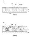
- FIGS. 1A through 1Eare partial cross-sectional views of a semiconductor structure and illustrate a method of forming a metal structure for a semiconductor device structure in accordance with embodiments of the present disclosure
- FIGS. 2A-2Fare partial cross-sectional views of a semiconductor structure and illustrate another method of forming a metal structure for a semiconductor device structure in accordance with embodiments of the present disclosure
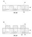
- FIGS. 3A-3Eare partial cross-sectional views of a semiconductor device structure and illustrate yet another method of forming a metal structure for a semiconductor device structure in accordance with embodiments of the present disclosure
- FIGS. 4A-4Gare partial cross-sectional views of a semiconductor device structure and illustrate yet still another method of forming a metal structure for a semiconductor device structure in accordance with embodiments of the present disclosure
- FIGS. 5A-5Fare partial cross-sectional views of a semiconductor device structure and illustrate yet still an additional method of forming a metal structure for a semiconductor device structure in accordance with embodiments of the present disclosure
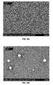
- FIG. 6Ais a scanning electron micrograph image showing a top-down view of copper particles formed on a semiconductor device structure, as described in Example 1;
- FIG. 6Bis a magnified scanning electron micrograph image showing a top-down view of a single copper particle formed on a semiconductor device structure, as described in Example 1;
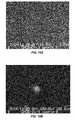
- FIG. 7Ais a graph of Auger analysis of the single copper particle shown in FIG. 6B , as described in Example 1;
- FIG. 7Bis an Auger electron map of the single copper particle shown in FIG. 6B , as described in Example 1;
- FIG. 8Ais a scanning electron micrograph image showing a top-down view of copper particles formed on a semiconductor device structure, as described in Example 2;
- FIG. 8Bis a magnified scanning electron micrograph image showing a top-down view of copper particles formed on a semiconductor device structure, as described in Example 2;
- FIG. 9Ais a scanning electron micrograph image showing a top-down view of copper particles formed on a semiconductor device structure, as described in Example 2;
- FIG. 9Bis a magnified scanning electron micrograph image showing a top-down view of copper particles formed on a semiconductor structure, as described in Example 2;
- FIG. 10Ais a scanning electron micrograph image showing a top-down view of copper particles formed on a semiconductor device structure, as described in Example 2;
- FIG. 10Bis a magnified scanning electron micrograph image showing a top-down view of a single copper particle formed on a semiconductor device structure, as described in Example 2;
- FIG. 11Ais a graph of Auger analysis of the single copper particle shown in FIG. 10B , as described in Example 2;
- FIG. 11Bis an Auger electron map of the single copper particle shown in FIG. 10B , as described in Example 2.
- the metal structureis formed from the selective and self-limited deposition of a metal, such as copper (Cu), silver (Ag), or alloys thereof.
- the metal structureis formed by complexing a metal precursor with a polymer that is configured to react with or couple to the metal precursor and has been applied to predetermined or patterned locations on a semiconductor substrate.
- the amount of metal precursor complexed with the polymeris limited at least by the amount of metal precursor applied to the polymer and the number of available binding or complexing sites in the polymer.
- the polymermay be removed and the metal precursor reduced to form the metal structure.
- the metal structuremay be an electrode or an interconnect.
- the metal structuremay be used as an active electrode for a memory cell of a conductive bridge random access memory (CBRAM) device.
- active electrodemeans and includes a conductive material, such as Cu or Ag, which serves as a source of metal ions (e.g., Cu + , Ag + ) for formation of the conductive bridge.
- the metal structuremay also be used as a conductive interface in a via, or as a nucleation site (e.g., a seed material) for subsequent metal deposition, such as electroless deposition.
- the selective and self-limited metal deposition processes disclosed hereinmay overcome difficulties with conventional processing of metals (e.g., difficulties processing Cu and Ag, such as difficulties etching and/or depositing Cu and Ag into small structures), decrease the deposition variability of current selective deposition technologies (e.g., electroless plating, autocatalytic deposition), and enable increased performance in semiconductor device structures (e.g., memory cells) and semiconductor devices (e.g., CBRAM devices) that rely on specific and uniform quantities of metal.
- difficulties processing Cu and Age.g., difficulties processing Cu and Ag, such as difficulties etching and/or depositing Cu and Ag into small structures
- decrease the deposition variability of current selective deposition technologiese.g., electroless plating, autocatalytic deposition
- semiconductor device structurese.g., memory cells
- semiconductor devicese.g., CBRAM devices
- FIGS. 1A through 1Eare simplified partial cross-sectional views illustrating embodiments of a method of forming at least one metal structure for a semiconductor device structure, such as an active electrode of a memory cell (e.g., for a CBRAM device), a conductive interface in a via, or a nucleation site.
- semiconductor device structure 100may include an electrode 102 , an active material 104 , and a block copolymer material 106 .
- the active material 104may be formed over and in contact with the first electrode 102
- the block copolymer material 106may be formed over and in contact with the active material 104 .
- the electrode 102may include any suitable conductive material including, but not limited to, a metal, a metal alloy, a conductive metal oxide, or combinations thereof.
- the first electrode 102may be formed from tungsten (W), tungsten nitride (WN), nickel (Ni), tantalum nitride (TaN), platinum (Pt), gold (Au), titanium nitride (TiN), titanium silicon nitride (TiSiN), titanium aluminum nitride (TiAlN), molybdenum nitride (MoN), or a combination thereof.
- the first electrode 102is formed from W.
- the electrode 102may be formed in, on, or over a substrate (not shown) using conventional techniques, such as chemical vapor deposition (CVD), physical vapor deposition (PVD), or atomic layer deposition (ALD).
- CVDchemical vapor deposition
- PVDphysical vapor deposition
- ALDatomic layer deposition
- substratemeans and includes a base material or construction upon which additional materials are formed.
- the substratemay be a semiconductor substrate, a base semiconductor layer on a supporting structure, a metal electrode or a semiconductor substrate having one or more layers, structures or regions fondled thereon.
- the substratemay be a conventional silicon substrate or other bulk substrate comprising a layer of semiconductive material.
- the term “bulk substrate”means and includes not only silicon wafers, but also silicon-on-insulator (SOI) substrates, such as silicon-on-sapphire (SOS) substrates and silicon-on-glass (SOG) substrates, epitaxial layers of silicon on a base semiconductor foundation, and other semiconductor or optoelectronic materials, such as silicon-germanium, germanium, gallium arsenide, gallium nitride, and indium phosphide.
- SOIsilicon-on-insulator
- SOSsilicon-on-sapphire
- SOOGsilicon-on-glass
- epitaxial layers of silicon on a base semiconductor foundationand other semiconductor or optoelectronic materials, such as silicon-germanium, germanium, gallium arsenide, gallium nitride, and indium phosphide.
- the substratemay be doped or undoped.
- the active material 104may be a solid state electrolyte material, such as at least one of a chalcogenide compound, a transition metal oxide, and a silicon oxide.
- a chalcogenide compoundrefers to a binary or multinary compound that includes at least one chalcogen and a more electropositive element or radical.
- chalcogenrefers to an element of Group VI of the Periodic Table, such as oxygen (O), sulfur (S), selenium (Se), or tellurium (Te).
- the electropositive elementmay include, but is not limited to, nitrogen (N), silicon (Si), nickel (Ni), gallium (Ga), germanium (Ge), arsenic (As), silver (Ag), indium (In), tin (Sn), antimony (Sb), gold (Au), lead (Pb), bismuth (Bi), or combinations thereof.
- the chalcogenide compoundmay be a binary, ternary, or quaternary alloy.
- the term “transition metal oxide”means and includes an oxide of an element of Groups VB, VIB, VIIB, VIII, IB, and IIB of the Periodic Table, such as copper oxide (CuO), cobalt oxide (CoO), iron oxide (Fe 2 O 3 ), nickel oxide (NiO), magnesium oxide (MnO 2 ), zinc oxide (ZnO), and titanium oxide (TiO 2 ).
- the silicon oxidemay, for example, be silicon dioxide (SiO 2 ).
- the active material 104is SiO 2 .
- the active material 104may be formed over and in contact with the electrode 102 using conventional techniques, such as CVD, PVD, or ALD.
- block copolymer materialmeans and includes a polymer material including two or more polymer blocks covalently bound to one or more polymer blocks of unlike type.
- the block copolymer material 106may be selected based on an ability of at least one polymer block to form a complex with a metal precursor, as described in further detail below.
- At least one of the polymer blocksmay include at least one functional group that is configured to interact with the metal precursor to form the complex.
- the block copolymer material 106may be a diblock copolymer material (i.e., copolymer material including two polymer blocks), a triblock copolymer (i.e., a copolymer material including three polymer blocks), or a multiblock copolymer (i.e., a copolymer material including more than three polymer blocks).
- the different polymer blocks of the block copolymer materialmay be substantially immiscible in one another.
- the block copolymer material 106may be a diblock copolymer including a hydrophobic block and a hydrophilic block.
- the hydrophobic blockmay include a polymer substantially insoluble in a solvent (e.g., an inert polar solvent, such as at least one of water and an organic solvent, such as an alcohol, tetrahydrofuran, and diemthylformamide).
- the hydrophilic blockmay include a polymer that swells upon contact with the solvent.
- the block copolymer materialis polystryene-block-poly-2-vinylpryidine (PS-2-P2VP).
- a ratio of the hydrophilic block to the hydrophobic blockmay be within a range of from about 80:20 by weight to about 50:50 by weight and, such as about 70:30 by weight.
- the block copolymer material 106may be applied over and in contact with the active material 104 by conventional techniques, such as spin casting, spin coating, spraying, ink coating, or dip coating.
- an annealing processmay be used to initiate phase separation between polymer blocks of the block copolymer material 106 ( FIG. 1A ) to form a block copolymer assembly 108 including at least two different domains.
- the block copolymer assembly 108may be formed from the block copolymer material 106 ( FIG. 1A ) by conventional self-assembly techniques, which are not described in detail herein.
- the at least two different domainsmay include at least one first domain 110 (e.g., at least one minority domain) and at least one second domain 112 (e.g., at least one majority domain).
- One or more of the at least one first domain 110 and the at least one second domain 112may include features (e.g., cylinders, or lamellae) that extend linearly along a direction normal to a planar surface (e.g., top surface) of at least one of the electrode 102 and the active material 104 .
- the block copolymer material 106FIG. 1A
- the at least one first domain 110may correspond to the hydrophilic block
- the at least one second domain 112may correspond to the hydrophobic block.
- the annealing processmay, for example, include at least one of thermal annealing (e.g., at a temperature greater than the glass transition temperature of the block copolymer material 106 and less than the degradation temperature of the block copolymer material 106 ), solvent vapor-assisted annealing (e.g., at a temperature greater than or equal to room temperature), and supercritical fluid-assisted annealing.
- the block copolymer material 106may be thermally annealed by exposing the block copolymer material 106 to a temperature within a range of from about 130° C. to about 275° C. in a vacuum or an inert atmosphere (e.g., a nitrogen atmosphere, an argon atmosphere, or combinations thereof).
- the block copolymer assembly 108may be exposed to a staining agent 114 to form a metal-complexed block copolymer assembly 116 including at least one metal-complexed domain 118 and at least one non-metal-complexed domain 120 .
- the at least one first domain 110may become the at least one metal-complexed domain 118 and the at least one second domain 112 ( FIG. 1B ) may become the at least one non-metal-complexed domain 120 .
- the at least one first domain 110may become the at least one non-metal-complexed domain 120 and the at least one second domain 112 ( FIG. 1B ) may become the at least one metal-complexed domain 118 .
- the staining agent 114may include at least one metal precursor 122 .
- the at least one metal precursor 122may be an elemental metal, an elemental metalloid, or a metal-containing compound capable of selectively coupling with the polymer of one or more domain(s) (e.g., the at least one first domain 110 ( FIG. 1B )) of the at least two different domains relative to the polymer of one or more other domain(s) (e.g., the at least one second domain 112 ( FIG. 1B )) of the at least two different domains.
- Suitable elemental metalsmay, for example, include copper, silver, ruthenium, cobalt, nickel, titanium, tungsten, tantalum, molybdenum, platinum, palladium, iridium, gold, and iron.
- Suitable elemental metalloidsmay, for example, include silicon, and germanium.
- Suitable metal-containing compoundsmay, for example, include metal oxides (e.g., metal alkoxide), and metal salts (e.g., metal halides, metal sulfates, metal cyanides, metal nitrides, and metal nitrates).
- the staining agent 114may also include at least one solvent.
- the at least one solventmay be a liquid, gas, or vapor capable of selectively permeating and swelling the one or more domain(s) (e.g., the at least one minority domain 110 ( FIG. 1B )) of the at least two different domains relative to the one or more other domain(s) (e.g., the at least one majority domain 112 ( FIG. 1B )) of the at least two different domains.
- the staining agent 114is a mixture of the metal precursor 122 and at least one solvent.
- Exposing the block copolymer assembly 108 ( FIG. 1B ) to the staining agent 114may form the metal-complexed block copolymer assembly 116 through at least one of chelation, other ligand interactions, and coulombic interactions.
- the metal precursor 122is an elemental metal or an elemental metalloid and the polymer of one or more domain(s) (e.g., the at least one first domain 110 ( FIG.
- the polymer of the one or more domain(s)may coordinate with the elemental metal or the elemental metalloid (e.g., charge-neutral forms, and charge-positive forms) through chelation and/or other ligand interactions.
- unsaturated organic groupsi.e., organic groups having ⁇ -orbital electrons
- element(s) of Groups VA and VIA of the Periodic table of Elementse.g., nitrogen, phosphorus, sulfur, and oxygen
- the polymer of the one or more domain(s)may coordinate with the elemental metal or the elemental metalloid (e.g., charge-neutral forms, and charge-positive forms) through chelation and/or other ligand interactions.
- the metal precursor 122may be selectively coupled to the polymer of one or more domain(s) (e.g., the at least one minority domain 110 ( FIG. 1B )) through coulombic interactions by providing a charge to the polymer of the one or more domain(s) opposing a charge provided to the metal-containing compound. For instance, if the polymer of one or more domain(s) (e.g., the at least one minority domain 110 ( FIG. 1B )) through coulombic interactions by providing a charge to the polymer of the one or more domain(s) opposing a charge provided to the metal-containing compound. For instance, if the polymer of one or more domain(s) (e.g., the at least one minority domain 110 ( FIG.
- the staining agent 114may be an aqueous acid solution including a metal-containing compound including anionic functionality (e.g., functional groups or constituents of the metal-containing compound that are or may become negatively charged).
- the polymer of one or more domain(s)e.g., the at least one minority domain 110 ( FIG.
- the staining agent 114may be an aqueous base solution including a metal-containing compound including cationic functionality (e.g., functional groups or constituents of the metal-containing compound that are or may become positively charged).
- Table 1 belowis a non-limiting list of materials and conditions that may be used in combination to form the at least one metal-complexed domain 118 of the metal-complexed block copolymer assembly 116 .
- the block copolymer assembly 108may be exposed to the solvent and the metal precursor 122 described above in a multiple act process.
- the block copolymer assembly 108may be exposed to the solvent prior to being exposed to the metal precursor 122 .
- Such a multiple act processmay be used to provide the at least one minority domain 110 ( FIG. 1B ) with an exposed surface (e.g., where the at least one minority domain 110 is covered by the majority domain 112 ), or to at least provide the at least one minority domain 110 ( FIG. 1B ) with additional surface area for interaction with the metal precursor 122 .
- a semiconductor device structure of the present disclosuremay include an electrode, and at least one metal-complexed structure (e.g., at least one metal-complexed domain) overlying the electrode and including at least one of an elemental metal, an elemental metalloid, a metal oxide, and a metal salt coupled to a polymer including features that extend linearly along a direction normal to a planar surface of the electrode.
- at least one metal-complexed structuree.g., at least one metal-complexed domain
- the polymer of the at least one non-metal-complexed domain 120may be volatized and removed from the metal-complexed block copolymer assembly 116 ( FIG. 1C ), and the metal precursor 122 ( FIG. 1C ) within the at least one metal-complexed domain 118 ( FIG. 1C ) may be reduced (i.e., chemically reduced) to form at least one metal structure 124 over and in contact with the active layer 104 .
- the at least one metal structure 124may be formed of a plurality of metal particles (not shown). Each metal particle of the plurality of metal particles may be discontinuous or discrete from each other metal particle of the plurality of metal particles.
- the polymermay, for example, be volatized and removed by performing a thermal anneal in a reducing atmosphere.
- the thermal annealmay expose the metal-complexed block copolymer assembly 116 ( FIG. 1C ) to a temperature greater than or equal to a decomposition temperature of the polymer of each of the at least one metal-complexed domain 118 ( FIG. 1C ) and the at least one non-metal-complexed domain 120 ( FIG. 1C ).
- the metal-complexed block copolymer assembly 116may be exposed to a temperature with a range of from about 250° C. to about 750° C. in at least one of an ammonia atmosphere and a hydrogen atmosphere. As shown in FIG.
- At least a portion of the metal structure 124may diffuse into the active layer 104 .
- Conventional processese.g., electroless plating
- the metal-complexed block copolymer assembly 116may, optionally, be exposed to an oxidizing agent (e.g., air, oxygen, nitrogen dioxide, water, nitrous oxide, dinitrogen tetroxide, ozone, or combinations thereof) prior to performing the thermal anneal in the reducing atmosphere described above. Exposure to the oxidizing agent may convert the metal precursor 122 ( FIG. 1C ) within the at least one metal-complexed domain 118 ( FIG. 1C ) to a metal oxide (not shown), which may then be reduced to metal by the thermal anneal in the reducing atmosphere.
- an oxidizing agente.g., air, oxygen, nitrogen dioxide, water, nitrous oxide, dinitrogen tetroxide, ozone, or combinations thereof
- the semiconductor device structure 100may be exposed to the oxidizing agent (e.g., ozone) in a sealed chamber at a temperature within a range of from about 25° C. to about 200° C., such as from about 75° C. to about 100° C., for a period of time within a range of from about 30 seconds to about 30 hours, such as from about 30 seconds to about 15 hours, or from about 30 seconds to about 1 hour, or from about 10 minutes to about 1 hour. Exposing the metal-complexed block copolymer assembly 116 ( FIG.
- the thermal anneal in the reducing atmospheremay be omitted, leaving a metal-oxide-complexed block copolymer assembly (not shown) including at least one metal-oxide-complexed domain (not shown) and at least one non-metal-oxide-complexed domain (not shown).
- Polymer of the metal-oxide-complexed block copolymer assemblymay be volatilized and removed (e.g., by way of a thermal anneal) to form at least one metal oxide structure.
- a method of forming a memory cellmay include forming a block copolymer assembly including at least two different domains over an electrode.
- the at least one metal precursormay be selectively coupled to the block copolymer assembly to form a metal-complexed block copolymer assembly including at least one metal-complexed domain and at least one non-metal-complexed domain.
- the metal-complexed block copolymer assemblymay be annealed to form at least one metal structure.
- a structure 126such as an electrode or a contact, may be formed over and in contact with the at least one metal structure 124 .
- the structure 126may, for example, include a suitable conductive material including, but not limited to, a metal, a metal alloy, a conductive metal oxide, or combinations thereof.
- the structure 126may be formed of W, WN, Ni, TaN, Pt, Ru, Co, CoSi, TiN, TiSiN, TiAlN, or MoN.
- the structure 126may be formed of substantially the same material as the electrode 102 or may be a different material than the electrode 102 .
- the structure 126is formed from W.
- the structure 126may be formed over and in contact with the at least one metal structure 124 using conventional deposition (e.g., CVD, ALD, or PVD) and patterning (e.g., masking and etching) techniques.
- FIGS. 2A through 2Fare simplified partial cross-sectional views of a semiconductor device structure 200 illustrating embodiments of another method of forming at least one metal structure for a semiconductor device structure, such as an active electrode of a memory cell (e.g., for a CBRAM device), a conductive interface in a via, or a nucleation site.
- the semiconductor substrate 200is substantially similar to the semiconductor substrate 100 described above, except that the metal structures are directly formed on an electrode.
- the semiconductor structure 200may include an electrode 202 , and a block copolymer material 206 .
- the block copolymer material 206may be formed over and in contact with the electrode 202 , which may be formed in, on, or over a substrate (not shown).
- the electrode 202 and the block copolymer material 206may be substantially similar to the electrode 102 and the block copolymer material 106 described above, respectively.
- the electrode 202 and the block copolymer material 206may be formed in a process substantially similar to that described above to form the electrode 102 and the block copolymer material 106 , respectively.
- an annealing processmay be used to initiate phase separation between blocks of the block copolymer material 206 to form a block copolymer assembly 208 including at least one minority domain 210 and at least one majority domain 212 .
- the annealing processmay be substantially similar to that described above with respect to formation of the block copolymer assembly 108 .
- the block copolymer assembly 208 , the at least one first domain 210 , and at least one second domain 212may be substantially similar to the block copolymer assembly 108 , the at least one first domain 110 , and at least one second domain 112 described above, respectively.
- FIG. 2Cthe block copolymer assembly 208 ( FIG.
- a staining agent 214at least including a metal precursor 222 to form a metal-complexed block copolymer assembly 216 including at least one metal-complexed domain 218 and at least one non-metal-complexed domain 220 .
- the processmay be substantially similar to that described above in relation to forming the metal-complexed block copolymer assembly 116 .
- the staining agent 214 , the metal-complexed block copolymer assembly 216 , the at least one metal-complexed domain 218 , and the at least one non-metal-complexed domain 220may be substantially similar to the staining agent 114 , the metal-complexed block copolymer assembly 116 , the at least one metal-complexed domain 118 , and the at least one non-metal-complexed domain 120 described above, respectively.
- polymer materialmay be volatized and removed from the metal-complexed block copolymer assembly 216 , and the metal precursor 222 ( FIG. 2C ) in the at least one metal-complexed domain 218 ( FIG. 2C ) may be reduced to form at least one metal structure 224 over and in contact with the electrode 202 .
- the at least one metal structure 224may be formed of a plurality of metal particles (not shown). Each metal particle of the plurality of metal particles may be discontinuous or discrete from each other metal particle of the plurality of metal particles. The process may be substantially similar to that described above in relation to forming the at least one metal structure 124 .
- the at least one metal structure 224may be substantially similar to the at least one metal structure 124 described above. Conventional processes (e.g., electroless plating) may, optionally, be used to increase the size of the metal particles (not shown) of the at least one metal structure 224 .
- the metal-complexed block copolymer assembly 216may, optionally, be exposed to an oxidizing agent before forming the at least one metal structure 224 . Exposure to the oxidizing agent may convert the metal precursor 222 ( FIG. 1C ) within the at least one metal-complexed domain 218 ( FIG. 2C ) to a metal oxide (not shown), which may then be reduced to metal by thermal anneal in a reducing atmosphere. The process may be substantially similar to that described above in relation to the treatment of the metal-complexed block copolymer assembly 116 . In additional embodiments, after exposing the metal-complexed block copolymer assembly 216 ( FIG.
- the thermal anneal in the reducing atmospheremay be omitted, leaving a metal-oxide-complexed block copolymer assembly (not shown) including at least one metal-oxide-complexed domain (not shown) and at least one non-metal-oxide-complexed domain (not shown).
- Polymer of the metal-oxide-complexed block copolymer assembly (not shown)may be volatilized and removed (e.g., by way of a thermal anneal) to form at least one metal oxide structure.
- an active material 204may be formed over and in contact with the at least one metal structure 224 and the electrode 202 .
- the active material 204may be substantially similar to the active material 104 described above, and may be formed using conventional techniques, such as CVD, PVD, or ALD, which are not described in detail herein.
- a structure 226such as an electrode or contact, may be formed over and in contact with the active material 204 at a position overlying the at least one metal structure 224 .
- the structure 226may be formed using conventional deposition and patterning techniques, which are not described in detail herein.
- the structure 226may be substantially similar to the structure 126 described above.
- FIGS. 3A through 3Eare simplified partial cross-sectional views of a semiconductor device structure 300 illustrating embodiments of yet another method of forming at least one metal structure for a semiconductor device structure, such as an active electrode of a memory cell (e.g., for a CBRAM device), a conductive interface in a via, or a nucleation site.
- the semiconductor device structure 300may include an electrode 302 , an active material 304 , and a polymer material 306 .
- the active material 304may be formed over and in contact with the electrode 302
- the polymer material 306may be formed over and in contact with the active material 304 .
- the electrode 302may be formed in, on, or over a substrate (not shown).
- the active material 304may, at least initially, be omitted, and the polymer material 306 may be formed over and in contact with the electrode 302 .
- the electrode 302 and the active material 304may be substantially similar to the electrode 102 and the active material 104 described above, respectively. Each of the electrode 302 and the active material 304 may be formed using conventional techniques, such as PVD, CVD, or ALD.
- the polymer material 306may be a homopolymer or a copolymer. As used herein, the term “homopolymer” means and includes a material resulting from the polymerization of a single monomeric species.
- the polymer material 306may be capable of forming a complex with a metal precursor.
- the polymer material 306may, by way of non-limiting example, be a hydrophilic polymer. In at least some embodiments, the polymer material 306 is poly-2-vinylpyridine (P2VP).
- the polymer material 306may be formed over and in contact with the active material 304 by conventional techniques, such as grafting.
- the polymer material 306may be prepared with end groups (e.g., hydroxyl groups) that may interact (e.g., by forming covalent bonds) with the active material 304 .
- a portion of the polymer material 306may be selectively removed to form a polymer pattern 308 including at least one polymer structure 310 and at least one opening 312 . Removing the portion of the polymer material 306 ( FIG. 3A ) may expose a surface of the active material 304 or, if the active material 304 is absent, a surface of the electrode 302 .
- the polymer pattern 308may be formed using conventional techniques. By way of non-limiting example, a resist material (not shown), such as a conventional photoresist or a conventional e-beam resist, may be applied over the polymer material 306 ( FIG.
- the patterned resistmay be transferred into the polymer material 306 ( FIG. 3A ) using at least one dry etching process, such as reactive ion etching (RIE), plasma etching, reactive ion beam etching, or chemically assisted ion beam etching.
- RIEreactive ion etching
- the patterned resistmay be removed using conventional techniques, such as a solvent strip utilizing a solvent with which the polymer is substantially immiscible.
- the polymer material 306may be a stainable photoresist including a blend of photoactive species and chemically active species. The photoactive species may enable photoimaging, and the chemically active species may enable staining.
- the polymer pattern 308( FIG. 3B ) may be exposed to a staining agent 314 to form a metal-complexed polymer pattern 316 including at least one metal-complexed polymer structure 318 and the at least one opening 312 .
- the staining agent 314 and process of forming the metal-complexed polymer pattern 316may be substantially similar to the staining agent 114 and process of forming of the metal-complexed copolymer assembly 116 described above.
- the staining agent 114may enable the selective coupling of the metal precursor 122 included therein with the polymer of the at least one minority domain 110
- the staining agent 314may enable the selective coupling of metal precursor 322 included therein with the polymer of the at least one polymer structure 310 ( FIG. 3B ).
- the polymer materialmay be volatized and removed from the at least one metal-complexed polymer structure 318 ( FIG. 3C ), and the metal precursor 322 ( FIG. 3C ) present therein may be reduced to form at least one metal structure 324 over and in contact with the active layer 304 .
- the processmay be substantially similar to that described above with respect to the formation of the at least one metal structure 124 .
- the at least one metal structure 324may be substantially similar to the at least one metal structure 124 described above and may be formed of a plurality of metal particles (not shown). Each metal particle of the plurality of metal particles may be discontinuous or discrete from each other metal particle of the plurality of metal particles. Conventional processes (e.g., electroless plating) may, optionally, used to increase the size of the metal particles (not shown) of the at least one metal structure 324 .
- the at least one metal-complexed polymer structure 318may, optionally, be exposed to an oxidizing agent before forming the at least one metal structure 324 . Exposure to the oxidizing agent may convert the metal precursor 322 ( FIG. 3C ) within the at least one metal-complexed polymer structure 318 ( FIG. 3C ) to a metal oxide (not shown), which may then be reduced to metal by thermal anneal in a reducing atmosphere. The process may be substantially similar to that described above in relation to the treatment of the metal-complexed block copolymer assembly 116 . In additional embodiments, after exposing the at least one metal-complexed polymer structure 318 ( FIG.
- the thermal anneal in the reducing atmospheremay be omitted, leaving at least one metal-oxide-complexed polymer structure (not shown).
- Polymer of the metal-oxide-complexed polymer structure (not shown)may be volatilized and removed (e.g., by way of a thermal anneal) to form at least one metal oxide structure.
- the at least one metal structure 324may be formed over and in contact with the electrode 302 , in a process substantially similar to that described above in relation to forming the at least one metal structure 224 .
- the active material 304may then be formed over and in contact with the at least one metal structure 324 and the electrode 302 , in a process substantially similar to that described above in relation to forming the active material 204 .
- a method of forming a memory cellmay include forming a polymer material over an electrode. A portion of the polymer material may be removed to form a polymer pattern including at least one polymer structure and at least one opening. The polymer pattern may be exposed to a staining agent to form a metal-complexed polymer pattern including at least one metal-complexed polymer structure. The metal-complexed polymer pattern may be treated to form at least one metal structure.
- a structure 326such as an electrode or contact, may be formed over and in contact with the at least one metal structure 324 .
- the structure 326may be formed using conventional deposition (e.g., CVD, ALD, or PVD) and patterning (e.g., masking and etching) techniques.
- the structure 326may be substantially similar to the structure 126 described above.
- the structure 326may be formed over and in contact with the active material 304 at a position overlying the at least one metal structure 324 , in a process substantially similar to that described above in relation to forming the structure 226 .
- FIGS. 4A through 4Gare simplified partial cross-sectional views of a semiconductor device structure 400 illustrating embodiments of yet still another method of forming at least one metal structure for a semiconductor device structure, such as an active electrode of a memory cell (e.g., for a CBRAM device), a conductive interface in a via, or a nucleation site.
- the semiconductor device structure 400may include an electrode 402 and a patterned dielectric material 404 .
- the patterned dielectric material 404may be formed over and in contact with the electrode 402 .
- the electrode 402may be substantially similar to the electrode 102 described above, and may be formed in, on, or over a substrate (not shown) using conventional techniques, such as PVD, CVD, or ALD.
- the patterned dielectric material 404may include at least one dielectric structure 406 and at least one opening 408 .
- the at least one opening 408may be defined by a surface 405 of the electrode 404 and at least one sidewall 407 of the at least one dielectric structure 406 .
- the at least one dielectric structure 406may, by way of non-limiting example, include at least one of silicon oxynitride (SiON), silicon nitride (Si 3 N 4 ), silicon dioxide (SiO 2 ), another oxide material, and another polymer material.
- the dielectric structure 406is formed from Si 3 N 4 .
- the patterned dielectric material 404may be formed using conventional deposition and patterning techniques, such as PVD, CVD, or ALD deposition followed by masking and etching.
- a conformal film of active material(not shown) may, optionally, be formed over and in contact with the patterned dielectric material 404 (e.g., the conformal film of active material may cover surfaces of the at least one dielectric structure 406 and the surface 405 of the electrode 404 ). If present, the conformal film of active material (not shown) may be substantially similar to the active material 104 described above, and may be formed using conventional techniques, such as PVD, CVD, or ALD.
- a polymer material 410may be formed over and in contact with a surface 412 of the at least one dielectric structure 406 , the at least one sidewall 407 of the at least one dielectric structure 406 , and the surface 405 of the electrode 404 exposed by the at least one opening 408 .
- the polymer material 410may cover or encompass the at least one dielectric structure 406 and may at least partially fill the at least one opening 408 .
- the polymer material 410substantially fills the at least one opening 408 .
- the polymer material 410may be substantially similar to the polymer material 306 described above.
- the polymer material 410is P2VP.
- the polymer material 410may be formed over and in contact with the patterned dielectric material 404 by conventional grafting techniques.
- the polymer material 410may be prepared with end groups (e.g., hydroxyl groups) that may interact (e.g., by forming covalent bonds) with one or more of the surface 412 of the at least one dielectric structure 406 , the at least one sidewall 407 of the at least one dielectric structure 406 , and the surface 405 of the electrode 404 exposed by the at least one opening 408 .
- end groupse.g., hydroxyl groups
- a portion of the polymer material 410may be removed to expose the surface 412 of the at least one dielectric structure 406 and form an assembly 414 including the at least one dielectric structure 406 and at least one polymer structure 416 .
- the portion of the polymer material 410may be removed using conventional techniques, such as at least one of an abrasive planarization process (e.g., chemical mechanical planarization), and a suitable etching process (e.g., wet etching, dry etching).
- the assembly 414( FIG. 4C ) may be exposed to a staining agent 418 to form a metal-complexed assembly 420 including at least one metal-complexed polymer structure 422 and the at least one dielectric structure 406 (i.e., a non-metal-complexed structure).
- the staining agent 418 and process of forming the metal-complexed assembly 420may be substantially similar to the staining agent 114 and process of forming of the metal-complexed copolymer assembly 116 described above.
- the staining agent 114may enable selective coupling of the metal precursor 122 included therein with the polymer of the at least one minority domain 110
- the staining agent 418may enable the selective coupling of a metal precursor 426 included therein with the polymer of the at least one polymer structure 416 ( FIG. 4C ).
- the polymer material 410may be exposed to the staining agent 418 to form a metal-complexed polymer material (not shown). A portion of the metal-complexed polymer material may then be removed to form the metal-complexed assembly 420 including the at least one metal-complexed polymer structure 422 and the at least one dielectric structure 406 .
- polymer materialmay be volatized and removed from the at least one metal-complexed polymer structure 422 ( FIG. 4D ), and the metal precursor 426 ( FIG. 4D ) present therein may be reduced to form at least one metal structure 428 over and in contact with the electrode 402 .
- the at least one metal structure 428may be formed from a plurality of metal particles (not shown). Each metal particle of the plurality of metal particles may be discontinuous or discrete from each other metal particle of the plurality of metal particles.
- the processmay be substantially similar to that described above in relation to forming the at least one metal structure 124 . However, as depicted in FIG. 4E , the at least one dielectric structure 406 may remain following the process.
- the at least one metal structure 428may be substantially similar to the at least one metal structure 124 described above. Conventional processes (e.g., electroless plating) may, optionally, be used to increase the size of the metal particles (not shown) of the at least one metal structure 428 .
- the at least one metal-complexed polymer structure 422may, optionally, be exposed to an oxidizing agent before forming the at least one metal structure 428 . Exposure to the oxidizing agent may convert the metal precursor 426 ( FIG. 4D ) within the at least one metal-complexed polymer structure 422 ( FIG. 4D ) to a metal oxide (not shown), which may then be reduced to metal by thermal anneal in a reducing atmosphere. The process may be substantially similar to that described above in relation to the treatment of the metal-complexed block copolymer assembly 116 . In additional embodiments, after exposing the at least one metal-complexed polymer structure 422 ( FIG.
- the thermal anneal in the reducing atmospheremay be omitted, leaving at least one metal-oxide-complexed polymer structure (not shown).
- Polymer of the metal-oxide-complexed polymer structure (not shown)may be volatilized and removed (e.g., by way of a thermal anneal) to form at least one metal oxide structure.
- an active material 430may be formed over and in contact with the at least one metal structure 428 and the at least one dielectric structure 406 .
- the active material 430may be formed using conventional techniques, such as CVD, PVD, or ALD.
- the active material 430may be substantially similar to the active material 104 described above.
- the active material 430may be selectively formed over and in contact with the at least one metal structure 428 (e.g., the active material 430 may be selectively grown on the at least one metal structure 428 ). As shown in FIG.
- a structure 432such as an electrode or contact, may be formed over and in contact with at least a portion of the active material 430 at a position overlying the at least one metal structure 428 .
- the structure 432may be substantially similar to the second electrode 126 described above, and may be formed using conventional deposition (e.g., CVD, ALD, or PVD) and patterning (e.g., masking and etching) techniques. At least a portion of the structure 432 may also contact the at least one dielectric structure 406 .
- FIGS. 5A through 5Fare simplified partial cross-sectional views of a semiconductor device structure 500 illustrating embodiments of yet still an additional method of forming at least one metal structure for a semiconductor structure, such as an active electrode of a memory cell (e.g., for a CBRAM device), a conductive interface in a via, or a nucleation site.
- the semiconductor structure 500include an electrode 502 , and a patterned dielectric material 504 .
- the electrode 502may be a conductive material (e.g., W, WN, Ni, TaN, Pt, Au, TiN, TiSiN, TiAlN, or MoN) that is reactive with a polymer material to be grafted on a surface 510 thereof, as described in further detail below.
- the patterned dielectric material 504may include at least one dielectric structure 506 and at least one opening 508 .
- the at least one opening 508may be defined by the surface 510 of the electrode 502 and at least one sidewall 511 of the dielectric structure 506 .
- the at least one dielectric structure 506may be a dielectric material (e.g., amorphous carbon) that is non-reactive with the polymer material to be grafted on the surface 510 of electrode 502 , as described in further detail below.
- a polymer material 512may be selectively grafted over and in contact with the surface 510 of the electrode 502 exposed by the at least one opening 508 to form an assembly 505 including the polymer material 512 and the dielectric structure 506 .
- the polymer material 512may be substantially similar to the polymer material 306 described above. In at least some embodiments, the polymer material 512 is P2VP.
- the polymer material 512may be selectively grafted over and in contact with the portion of the surface 510 by conventional grafting techniques.
- the polymer material 512may be prepared with end groups (e.g., hydroxyl groups) that may interact (e.g., by forming covalent bonds) with the surface 510 of the electrode 502 .
- the dielectric structure 506may be substantially non-reactive with the polymer material 512 such that the polymer material 512 does not become grafted to the at least one sidewall 511 of the dielectric structure 506 .
- a suitable rinsemay, optionally, be performed to remove portions of the polymer material 512 not grafted to the surface 510 of the electrode 502 .
- the assembly 505( FIG. 5B ) may be exposed to a staining agent 514 to form a metal-complexed assembly 516 including at least one metal-complexed polymer structure 518 and the at least one dielectric structure 506 (i.e., a non-metal-complexed structure).
- the staining agent 514 and process of forming the metal-complexed assembly 516may be substantially similar to the staining agent 114 and process of forming of the metal-complexed copolymer assembly 116 described above.
- the staining agent 114may enable selective coupling of the metal precursor 122 included therein with the polymer of the at least one minority domain 110
- the staining agent 514may enable the selective coupling of a metal precursor 520 included therein with the polymer of the at least one polymer material 512 ( FIG. 5B ).
- polymer materialmay be volatized and removed from the at least one metal-complexed polymer structure 518 ( FIG. 5C ), and the metal precursor 520 ( FIG. 5C ) present therein may be reduced to form at least one metal structure 522 over and in contact with the electrode 502 .
- the at least one metal structure 522may include a plurality of metal particles (not shown). Each metal particle of the plurality of metal particles may be discontinuous or discrete from each other metal particle of the plurality of metal particles. Conventional processes (e.g., electroless plating) may, optionally, be used to increase the size of the metal particles (not shown) of the at least one metal structure 522 .
- the process of forming the metal structure 522may be substantially similar to that described above with respect to the formation the at least one metal structure 124 . However, as depicted in FIG. 5D , the at least one dielectric structure 506 may remain following the process.
- the at least one metal-complexed polymer structure 518may, optionally, be exposed to an oxidizing agent before forming the at least one metal structure 522 . Exposure to the oxidizing agent may convert the metal precursor 520 ( FIG. 5C ) within the at least metal-complexed polymer structure 518 ( FIG. 5C ) to a metal oxide (not shown), which may then be reduced to metal by thermal anneal in a reducing atmosphere. The process may be substantially similar to that described above in relation to the treatment of the metal-complexed block copolymer assembly 116 . In additional embodiments, after exposing the at least one metal-complexed polymer structure 518 ( FIG.
- the thermal anneal in the reducing atmospheremay be omitted, leaving at least one metal-oxide-complexed polymer structure (not shown).
- Polymer of the at least one metal-oxide-complexed polymer structure (not shown)may be volatilized and removed (e.g., by way of a thermal anneal) to form at least one metal oxide structure.
- a method of forming a memory cellmay include forming a patterned dielectric material including at least one dielectric structure and at least one opening over an electrode.
- a polymer materialmay be formed over and in contact with at least a surface of the electrode exposed by the at least one opening.
- the at least one dielectric structure and the polymer materialmay be exposed to a staining agent to form a metal-complexed assembly including at least one metal-complexed polymer structure.
- the metal-complexed assemblymay be treated to form at least one metal structure.
- an active material 524may be formed over and in contact with the at least one metal structure 522 and the at least one dielectric structure 506 .
- the active material 524may be formed using conventional techniques, such as CVD, PVD, or ALD.
- the active material 524may be substantially similar to the active material 104 described above.
- the at least one dielectric structure 506may be removed and the active material 524 may be formed over and in contact with the at least one metal structure and the electrode 502 .
- a structure 526such as an electrode or contact, may be formed over and in contact with at least a portion of the active material 524 at a position overlying the at least one metal structure 522 .
- the structure 526may be substantially similar to the structure 126 described above, and may be formed using conventional deposition (e.g., CVD, ALD, or PVD) and patterning (e.g., masking and etching) techniques. At least a portion of the structure 526 may also contact the at least one dielectric structure 506 , if present.
- CVDchemical vapor deposition
- ALDatomic layer deposition
- PVDphysical vapor deposition
- patterninge.g., masking and etching
- the methods of the present disclosureadvantageously reduce metal processing, decrease material deposition variability relative to conventional selective deposition technologies, such as electroless plating, and enable the formation of semiconductor structures, memory cells, and semiconductor devices that exhibit increased reliability, performance, and durability.
- the methods of the present disclosureenable the deposition of material on electrochemically inactive materials (e.g., dielectric materials, such as oxide materials) where conventional selective deposition technologies, such as electroless plating, may be substantially ineffective.
- Structuresmay be formed in desired locations on a substantially planar material (e.g., an electrode (i.e., a conductive material) or an active material), or in openings in a patterned material (e.g., a patterned dielectric material) that overlies a substantially planar material.
- a substantially planar materiale.g., an electrode (i.e., a conductive material) or an active material
- a patterned materiale.g., a patterned dielectric material
- FIG. 6Ais a scanning electron micrograph (SEM) image showing a top-down view of white particles formed from the sample F.
- FIG. 6Bis a magnified SEM image showing a top-down view of a single white particle formed from sample F illustrating the two areas used for Auger analysis.
- the chart of Auger analysis of sample Fis shown in FIG. 7A .
- Particles formed from samples H and Jhad similar results.
- An Auger electron map of the white particle shown in FIG. 6Bis shown in FIG. 7B .
- the XPS analysis resultsare shown in Table 3 below.
- samples 1, 2, 3, and 4respectively correspond to samples F, H, J, and L of Table 2.
- the Auger and XPS analysis resultsshowed that the white particles formed from sample F (i.e., sample 1 in Table 3 below) were copper and had both CuO and either Cu 2 O or Cu(0) metal composition. No chlorine atoms were detected, indicating that the particles were fully reduced and then subsequently re-oxidized by atmospheric oxygen.
- the particles formed from samples F, H, J, and Lhad center diameters ranging from about 50 nm to about 250 nm.
- FIGS. 8A and 8Bare SEM images (i.e., at 10 k and 100 k magnification, respectively) showing a top-down view of white particles formed from the sample including 10 wt % CuCl 2 loading.
- FIGS. 9A and 9Bare SEM images (i.e., at 10 k and 100 k magnification, respectively) showing a top-down view of white particles formed from the sample including 2 wt % CuCl 2 loading.
- FIG. 10Ais a scanning electron micrograph (SEM) image showing a top-down view of white particles formed from a sample B including 2 wt % CuCl 2 .
- FIG. 10Bis a magnified SEM image showing a top-down view of a single white particle formed from sample B illustrating the two areas used for Auger analysis.
- the chart of Auger analysis of sample Bis shown in FIG. 11A .
- An Auger electron map of the white particle shown in FIG. 10Bis shown in FIG. 11B .
- the Auger analysis resultsshowed that the white particles formed from sample B were copper.
Landscapes
- Engineering & Computer Science (AREA)
- Manufacturing & Machinery (AREA)
- Semiconductor Memories (AREA)
Abstract
Description
| TABLE 1 |
| Exemplary Materials and Conditions for |
| Forming the Metal- |
| Domain | Complexation | Binding | Metal |
| polymer | pH | Functionality | precursor |
| Poly(vinylpyridine) | less than 7 | Pyridinium | Ammonium |
| (i.e., acidic) | silver (I) | ||
| thiosulfate | |||
| Poly(vinylpyridine) | less than 7 | Pyridinium | Copper (II) |
| (i.e., acidic) | chloride | ||
| Poly((meth)acrylic acid) | greater than 7 | Carboxylic acid | Silver (I) |
| (i.e., basic) | nitrate | ||
| Poly((meth)acrylic acid) | greater than 7 | Carboxylic acid | Copper (I) |
| (i.e., basic) | chloride | ||
| TABLE 2 |
| Sample Data |
| Sample | wt % CuCl2 | Reducing atmosphere |
| F | 10 | H2 |
| H | 10 | NH3 |
| J | 2 | H2 |
| L | 2 | NH3 |
| TABLE 3 |
| XPS Analysis Data |
| Surface elemental concentrations (in atom %) |
| Sample | C | N | O | F | So | Zr | Cu(o)/Cu(I) | Cu(II) |
| 1 | 14.8 | 8.6 | 49.0 | 0.5 | 8.4 | 16.4 | 0.8 | 1.5 | |
| 2 | 39.9 | 3.0 | 32.5 | 10.3 | 3.2 | 11.2 | ND | ||
| 3 | 16.2 | 7.4 | 49.5 | 0.5 | 8.3 | 18.0 | ND | ND | |
| 4 | 32.2 | 2.7 | 44.3 | 0.6 | 7.0 | 13.2 | ND | ND | |
Claims (30)
Priority Applications (2)
| Application Number | Priority Date | Filing Date | Title |
|---|---|---|---|
| US13/287,814US8900963B2 (en) | 2011-11-02 | 2011-11-02 | Methods of forming semiconductor device structures, and related structures |
| US14/546,897US9431605B2 (en) | 2011-11-02 | 2014-11-18 | Methods of forming semiconductor device structures |
Applications Claiming Priority (1)
| Application Number | Priority Date | Filing Date | Title |
|---|---|---|---|
| US13/287,814US8900963B2 (en) | 2011-11-02 | 2011-11-02 | Methods of forming semiconductor device structures, and related structures |
Related Child Applications (1)
| Application Number | Title | Priority Date | Filing Date |
|---|---|---|---|
| US14/546,897DivisionUS9431605B2 (en) | 2011-11-02 | 2014-11-18 | Methods of forming semiconductor device structures |
Publications (2)
| Publication Number | Publication Date |
|---|---|
| US20130105755A1 US20130105755A1 (en) | 2013-05-02 |
| US8900963B2true US8900963B2 (en) | 2014-12-02 |
Family
ID=48171437
Family Applications (2)
| Application Number | Title | Priority Date | Filing Date |
|---|---|---|---|
| US13/287,814Active2032-09-11US8900963B2 (en) | 2011-11-02 | 2011-11-02 | Methods of forming semiconductor device structures, and related structures |
| US14/546,897ActiveUS9431605B2 (en) | 2011-11-02 | 2014-11-18 | Methods of forming semiconductor device structures |
Family Applications After (1)
| Application Number | Title | Priority Date | Filing Date |
|---|---|---|---|
| US14/546,897ActiveUS9431605B2 (en) | 2011-11-02 | 2014-11-18 | Methods of forming semiconductor device structures |
Country Status (1)
| Country | Link |
|---|---|
| US (2) | US8900963B2 (en) |
Cited By (19)
| Publication number | Priority date | Publication date | Assignee | Title |
|---|---|---|---|---|
| US9257256B2 (en) | 2007-06-12 | 2016-02-09 | Micron Technology, Inc. | Templates including self-assembled block copolymer films |
| US9431605B2 (en) | 2011-11-02 | 2016-08-30 | Micron Technology, Inc. | Methods of forming semiconductor device structures |
| US9682857B2 (en) | 2008-03-21 | 2017-06-20 | Micron Technology, Inc. | Methods of improving long range order in self-assembly of block copolymer films with ionic liquids and materials produced therefrom |
| US9768021B2 (en) | 2007-04-18 | 2017-09-19 | Micron Technology, Inc. | Methods of forming semiconductor device structures including metal oxide structures |
| US20180173109A1 (en)* | 2016-12-15 | 2018-06-21 | Imec Vzw | Lithographic Mask Layer |
| US10005308B2 (en) | 2008-02-05 | 2018-06-26 | Micron Technology, Inc. | Stamps and methods of forming a pattern on a substrate |
| US10026606B2 (en)* | 2016-07-13 | 2018-07-17 | Tokyo Electron Limited | Method for depositing a silicon nitride film |
| US10049874B2 (en) | 2013-09-27 | 2018-08-14 | Micron Technology, Inc. | Self-assembled nanostructures including metal oxides and semiconductor structures comprised thereof |
| US10153200B2 (en) | 2008-03-21 | 2018-12-11 | Micron Technology, Inc. | Methods of forming a nanostructured polymer material including block copolymer materials |
| US10636648B2 (en) | 2017-12-04 | 2020-04-28 | Tokyo Electron Limited | Film deposition method of depositing film and film deposition apparatus |
| US10643837B2 (en) | 2017-08-09 | 2020-05-05 | Tokyo Electron Limited | Method for depositing a silicon nitride film and film deposition apparatus |
| US10748758B2 (en) | 2017-08-09 | 2020-08-18 | Tokyo Electron Limited | Method for depositing a silicon nitride film and film deposition apparatus |
| US10844487B2 (en) | 2017-02-22 | 2020-11-24 | Tokyo Electron Limited | Film deposition method and film deposition apparatus |
| US11120941B2 (en)* | 2018-01-24 | 2021-09-14 | Semiconductor Components Industries, Llc | Methods of forming capacitors |
| US11404265B2 (en) | 2019-01-30 | 2022-08-02 | Tokyo Electron Limited | Film deposition method |
| US20220254998A1 (en)* | 2019-08-30 | 2022-08-11 | National University Corporation Tottori University | Conductive bridge memory device, manufacturing method thereof, and switching device |
| US11952661B2 (en) | 2018-07-13 | 2024-04-09 | Tokyo Electron Limited | Deposition method |
| US12398324B1 (en) | 2024-05-30 | 2025-08-26 | Tokyo Electron Limited | Methods for controlling the pitch of self-assembled ionic liquid crystal (ILC) structures |
| US12444606B2 (en) | 2023-11-09 | 2025-10-14 | Tokyo Electron Limited | Methods for forming vertically layered ionic liquid crystal (ILC) structures on a semiconductor substrate |
Families Citing this family (4)
| Publication number | Priority date | Publication date | Assignee | Title |
|---|---|---|---|---|
| KR101490405B1 (en)* | 2012-10-19 | 2015-02-06 | 주식회사 엘지화학 | Forming method of metal nano-structure of metal nano-wire pattern or metal nano-mesh pattern |
| CN105474420B (en)* | 2013-03-15 | 2018-12-14 | Adesto技术公司 | Non-volatile memory with half-metal or semiconductor electrodes |
| US20150160072A1 (en)* | 2013-12-06 | 2015-06-11 | Rensselaer Polytechnic Institute | Oriented backscattering wide dynamic-range optical radiation sensor |
| JP2016066644A (en)* | 2014-09-22 | 2016-04-28 | 株式会社東芝 | Manufacturing method of storage device |
Citations (298)
| Publication number | Priority date | Publication date | Assignee | Title |
|---|---|---|---|---|
| US4623674A (en) | 1985-06-21 | 1986-11-18 | Union Carbide Corporation | Polymer/polyols of substituted styrenes and polyurethanes made therefrom |
| US4797357A (en) | 1986-05-30 | 1989-01-10 | Eastman Kodak Company | Light-stable reducible compounds and analytical compositions, elements and methods utilizing same |
| US4818713A (en) | 1987-10-20 | 1989-04-04 | American Telephone And Telegraph Company, At&T Bell Laboratories | Techniques useful in fabricating semiconductor devices having submicron features |
| US4877647A (en) | 1986-04-17 | 1989-10-31 | Kansas State University Research Foundation | Method of coating substrates with solvated clusters of metal particles |
| WO1990007575A1 (en) | 1988-12-30 | 1990-07-12 | Anderson David M | Stabilized microporous materials and hydrogel materials |
| US5328810A (en) | 1990-05-07 | 1994-07-12 | Micron Technology, Inc. | Method for reducing, by a factor or 2-N, the minimum masking pitch of a photolithographic process |
| US5374367A (en) | 1992-08-07 | 1994-12-20 | Fujikura Kasei Co., Ltd. | Electro-sensitive composition |
| US5382373A (en) | 1992-10-30 | 1995-01-17 | Lord Corporation | Magnetorheological materials based on alloy particles |
| US5482656A (en) | 1993-03-04 | 1996-01-09 | Kabushiki Kaisha Toshiba | Non-linear optical devices employing a polysilane composition and a polysilane composition therefor |
| US5512131A (en) | 1993-10-04 | 1996-04-30 | President And Fellows Of Harvard College | Formation of microstamped patterns on surfaces and derivative articles |
| US5538655A (en) | 1994-06-29 | 1996-07-23 | Arthur D. Little, Inc. | Molecular complexes for use as electrolyte components |
| US5580700A (en) | 1992-11-25 | 1996-12-03 | Hoechst Celanese Corporation | Metal ion reduction in bottom anti-reflective coatings for use in semiconductor device formation |
| WO1997006013A1 (en) | 1995-08-04 | 1997-02-20 | International Business Machines Corporation | Lithographic surface or thin layer modification |
| US5620850A (en) | 1994-09-26 | 1997-04-15 | President And Fellows Of Harvard College | Molecular recognition at surfaces derivatized with self-assembled monolayers |
| US5622668A (en) | 1992-02-07 | 1997-04-22 | The United States Of America As Represented By The Secretary Of The Air Force | Method for preparing oriented polymer structures and said structures |
| US5772905A (en) | 1995-11-15 | 1998-06-30 | Regents Of The University Of Minnesota | Nanoimprint lithography |
| WO1998039645A1 (en) | 1997-03-07 | 1998-09-11 | Beckman Coulter, Inc. | A novel capillary |
| US5834583A (en) | 1995-07-27 | 1998-11-10 | Circe Biomedical, Inc. | Block copolymers |
| US5849810A (en) | 1993-08-06 | 1998-12-15 | Ciba Vision Corporation | Photocrosslinked polymers |
| US5879853A (en) | 1996-01-18 | 1999-03-09 | Kabushiki Kaisha Toshiba | Top antireflective coating material and its process for DUV and VUV lithography systems |
| US5879582A (en) | 1994-08-19 | 1999-03-09 | The Lubrizol Corporation | Electrorheological fluids of polar solids and organic semiconductors |
| JPH1180414A (en) | 1997-08-29 | 1999-03-26 | Res Dev Corp Of Japan | Double structure continuous porous body and method for producing the same |
| US5891356A (en) | 1990-08-30 | 1999-04-06 | Asahi Kasei Kogyo Kabushiki Kaisha | Homogeneous electrorheological fluid |
| US5948470A (en) | 1997-04-28 | 1999-09-07 | Harrison; Christopher | Method of nanoscale patterning and products made thereby |
| WO1999047570A1 (en) | 1998-03-18 | 1999-09-23 | University Of Rochester | Macromolecular self-assembly of microstructures, nanostructures, objects and mesoporous solids |
| US5958704A (en) | 1997-03-12 | 1999-09-28 | Ddx, Inc. | Sensing system for specific substance and molecule detection |
| US6051869A (en) | 1996-06-26 | 2000-04-18 | Intel Corporation | Silicon-rich block copolymers to achieve unbalanced vias |
| WO2000031183A1 (en) | 1998-11-24 | 2000-06-02 | The Dow Chemical Company | A composition containing a cross-linkable matrix precursor and a poragen, and a porous matrix prepared therefrom |
| US6111323A (en) | 1997-12-30 | 2000-08-29 | International Business Machines Corporation | Reworkable thermoplastic encapsulant |
| US6153495A (en) | 1998-03-09 | 2000-11-28 | Intersil Corporation | Advanced methods for making semiconductor devices by low temperature direct bonding |
| US6207787B1 (en) | 1994-07-27 | 2001-03-27 | International Business Machines Corporation | Antireflective coating for microlithography |
| US6251791B1 (en) | 1999-07-20 | 2001-06-26 | United Microelectronics Corp. | Eliminating etching microloading effect by in situ deposition and etching |
| US6270946B1 (en) | 1999-03-18 | 2001-08-07 | Luna Innovations, Inc. | Non-lithographic process for producing nanoscale features on a substrate |
| US20010024768A1 (en) | 1996-02-26 | 2001-09-27 | Matsushita Electric Industrial Co., Ltd. | Pattern forming material and pattern forming method |
| US6309580B1 (en) | 1995-11-15 | 2001-10-30 | Regents Of The University Of Minnesota | Release surfaces, particularly for use in nanoimprint lithography |
| US6310138B1 (en) | 1998-06-05 | 2001-10-30 | Asahi Kasei Kabushiki Kaisha | Hydrogenated block copolymer and polypropylene resin composition containing the same |
| US6312971B1 (en) | 1999-08-31 | 2001-11-06 | E Ink Corporation | Solvent annealing process for forming a thin semiconductor film with advantageous properties |
| US20010049195A1 (en) | 2000-02-25 | 2001-12-06 | Chartered Semiconductor Manufacturing Ltd. | Non-metallic barrier formations for copper damascene type interconnects |
| WO2002018080A1 (en) | 2000-08-03 | 2002-03-07 | Upepo & Maji Inc. | Metal colloidal solution composition and conductor or ink for forming semiconductor pattern comprising it and method for forming conductor or semiconductor pattern |
| US6368871B1 (en) | 1997-08-13 | 2002-04-09 | Cepheid | Non-planar microstructures for manipulation of fluid samples |
| US20020055239A1 (en) | 2000-03-22 | 2002-05-09 | Mark Tuominen | Nanocylinder arrays |
| US6403382B1 (en) | 1998-12-08 | 2002-06-11 | Regents Of The University Of Minnesota | Attachment chemistry for organic molecules to silicon |
| US6414164B1 (en) | 2000-07-12 | 2002-07-02 | International Business Machines Corporation | Synthesis of soluble derivatives of sexithiophene and their use as the semiconducting channels in thin-film filed-effect transistors |
| US20020084429A1 (en) | 2000-10-17 | 2002-07-04 | Craighead Harold G. | Electron-beam patterning of functionalized self-assembled monolayers |
| US6423474B1 (en) | 2000-03-21 | 2002-07-23 | Micron Technology, Inc. | Use of DARC and BARC in flash memory processing |
| US6423465B1 (en) | 2000-01-28 | 2002-07-23 | International Business Machines Corporation | Process for preparing a patterned continuous polymeric brush on a substrate surface |
| WO2002081372A2 (en) | 2001-04-06 | 2002-10-17 | Carnegie Mellon University | A process for the preparation of nanostructured materials |
| US20020158342A1 (en) | 2001-03-14 | 2002-10-31 | Mark Tuominen | Nanofabrication |
| US6503841B1 (en) | 2000-07-07 | 2003-01-07 | Agere Systems Inc. | Oxide etch |
| US6506660B2 (en) | 2000-11-15 | 2003-01-14 | International Business Machines Corporation | Semiconductor with nanoscale features |
| US20030010241A1 (en) | 2001-03-28 | 2003-01-16 | Masamichi Fujihira | Patterning method with micro- contact printing and its printed product |
| US6518194B2 (en) | 2000-12-28 | 2003-02-11 | Thomas Andrew Winningham | Intermediate transfer layers for nanoscale pattern transfer and nanostructure formation |
| US6517933B1 (en) | 2000-01-18 | 2003-02-11 | Nano-Tex, Llc | Hybrid polymer materials |
| US6537920B1 (en) | 2001-03-16 | 2003-03-25 | Advanced Micro Devices, Inc. | Formation of vertical transistors using block copolymer lithography |
| US20030068639A1 (en) | 2001-08-31 | 2003-04-10 | Thomas Haneder | Detecting biochemical reactions |
| US6548830B1 (en) | 1996-05-22 | 2003-04-15 | Sony Corporation | Semiconductor device formed of single crystal grains in a grid pattern |
| US20030077452A1 (en) | 2001-07-17 | 2003-04-24 | Guire Patrick E. | Self assembling monolayer compositions |
| US20030080471A1 (en) | 2001-10-29 | 2003-05-01 | Chou Stephen Y. | Lithographic method for molding pattern with nanoscale features |
| US20030091752A1 (en) | 2001-10-05 | 2003-05-15 | Nealey Paul F. | Guided self-assembly of block copolymer films on interferometrically nanopatterned substrates |
| US6565763B1 (en) | 1999-06-07 | 2003-05-20 | Kabushiki Kaisha Toshiba | Method for manufacturing porous structure and method for forming pattern |
| US6565764B2 (en) | 2000-08-11 | 2003-05-20 | Kabushiki Kaisha Toshiba | Method of manufacturing a material having a fine structure |
| US6566248B1 (en) | 2001-01-11 | 2003-05-20 | Advanced Micro Devices, Inc. | Graphoepitaxial conductor cores in integrated circuit interconnects |
| US6569528B2 (en) | 2001-06-23 | 2003-05-27 | Pacific Corporation | Amphiphilic biodegradable block copolymers and self-assembled polymer aggregates formed from the same in aqueous milieu |
| JP2003155365A (en) | 2001-11-22 | 2003-05-27 | Toshiba Corp | Processing method and molded body |
| US20030100822A1 (en) | 2001-09-01 | 2003-05-29 | Seok Lew | Analyte measuring biosensor chip using image scanning system |
| US6573030B1 (en) | 2000-02-17 | 2003-06-03 | Applied Materials, Inc. | Method for depositing an amorphous carbon layer |
| US20030108879A1 (en) | 2001-01-10 | 2003-06-12 | Symyx Technologies, Inc. | Polymer brushes for immobilizing molecules to a surface or substrate having improved stability |
| US6592764B1 (en) | 1997-12-09 | 2003-07-15 | The Regents Of The University Of California | Block copolymer processing for mesostructured inorganic oxide materials |
| US20030157248A1 (en) | 2001-11-21 | 2003-08-21 | Watkins James J. | Mesoporous materials and methods |
| US20030178707A1 (en) | 2002-03-21 | 2003-09-25 | Abbott Donald C. | Preplated stamped small outline no-lead leadframes having etched profiles |
| US20030180522A1 (en) | 2002-03-22 | 2003-09-25 | Desimone Joseph M. | Methods of forming polymeric structures using carbon dioxide and polymeric structures formed thereby |
| US20030180966A1 (en) | 2002-03-20 | 2003-09-25 | Wisconsin Alumni Research Foundation | Optical imaging of nanostructured substrates |
| US6635912B2 (en) | 2000-09-07 | 2003-10-21 | Nec Electronics Corporation | CMOS image sensor and manufacturing method thereof |
| US6656308B2 (en) | 2002-04-22 | 2003-12-02 | International Business Machines Corporation | Process of fabricating a precision microcontact printing stamp |
| US20030235930A1 (en) | 2002-06-25 | 2003-12-25 | Lucent Technologies Inc. | Multi-impression nanofeature production |
| US6679996B1 (en) | 1999-10-05 | 2004-01-20 | Hoya Corporation | Metal oxide pattern forming method |
| US6682660B2 (en) | 1998-09-04 | 2004-01-27 | Mds Proteomics, Inc. | Ultrasonically generated paramagnetic polymer particles |
| US20040023287A1 (en) | 2002-08-02 | 2004-02-05 | Oliver Harnack | Method of attaching hydrophilic species to hydrophilic macromolecules and immobilizing the hydrophilic macromolecules on a hydrophobic surface |
| US20040028875A1 (en) | 2000-12-02 | 2004-02-12 | Van Rijn Cornelis Johannes Maria | Method of making a product with a micro or nano sized structure and product |
| US6699797B1 (en) | 2002-12-17 | 2004-03-02 | Intel Corporation | Method of fabrication of low dielectric constant porous metal silicate films |
| US20040058059A1 (en) | 2001-11-07 | 2004-03-25 | Linford Mathew Richard | Funtionalized patterned surfaces |
| US6713238B1 (en) | 1998-10-09 | 2004-03-30 | Stephen Y. Chou | Microscale patterning and articles formed thereby |
| TW584670B (en) | 2002-10-31 | 2004-04-21 | Academia Sinica | Fabrication of nanocomposite thin films for high density magnetic recording media |
| US20040084298A1 (en) | 2002-10-31 | 2004-05-06 | Y.D. Yao | Fabrication of nanocomposite thin films for high density magnetic recording media |
| EP1416303A2 (en) | 2002-10-30 | 2004-05-06 | Hitachi, Ltd. | Functioning substrate with a group of columnar micro pillars and its manufacturing method |
| US20040124092A1 (en) | 2002-12-30 | 2004-07-01 | Black Charles T. | Inorganic nanoporous membranes and methods to form same |
| US20040127001A1 (en) | 2002-12-27 | 2004-07-01 | International Business Machines Corporation | Robust ultra-low k interconnect structures using bridge-then-metallization fabrication sequence |
| US20040142578A1 (en) | 2002-03-28 | 2004-07-22 | Ulrich Wiesner | Thin film nanostructures |
| US6767693B1 (en) | 2002-07-30 | 2004-07-27 | Advanced Micro Devices, Inc. | Materials and methods for sub-lithographic patterning of contact, via, and trench structures in integrated circuit devices |
| US20040159633A1 (en) | 1993-10-04 | 2004-08-19 | President & Fellows Of Harvard University | Methods of etching articles via micro contact printing |
| US6781166B2 (en) | 1999-07-02 | 2004-08-24 | President & Fellows Of Harvard College | Nanoscopic wire-based devices and arrays |
| US6780492B2 (en) | 1999-03-02 | 2004-08-24 | International Business Machines Corporation | Substrates prepared by chemical amplification of self-assembled monolayers with spatially localized polymer brushes |
| US20040163758A1 (en) | 2000-04-21 | 2004-08-26 | International Business Machines Corporation | Patterning solution deposited thin films with self-assembled monolayers |
| US6797202B2 (en) | 1996-09-06 | 2004-09-28 | Bridgestone Corporaton | Particles for electro-rheological fluid |
| US20040192013A1 (en) | 2003-03-31 | 2004-09-30 | Ryu Myung Kwan | Method for fabricating single crystal silicon film |
| US6809210B2 (en) | 2001-06-12 | 2004-10-26 | Lucent Technologies Inc. | Method of solvating a metal in an aromatic organic liquid |
| US6812132B2 (en) | 2003-03-21 | 2004-11-02 | Intel Corporation | Filling small dimension vias using supercritical carbon dioxide |
| US20040222415A1 (en) | 2003-03-11 | 2004-11-11 | Industrial Technology Research Institute | Organic device including semiconducting layer aligned according to microgrooves of photoresist layer |
| JP2004335962A (en) | 2003-05-12 | 2004-11-25 | Seiko Epson Corp | Thin-film pattern forming method, device and manufacturing method thereof, electro-optical device, and electronic apparatus |
| US20040254317A1 (en) | 2003-06-12 | 2004-12-16 | Jinlian Hu | Methods for producing di-block polymers |
| US20040256615A1 (en) | 2001-07-09 | 2004-12-23 | Henning Sirringhaus | Lamellar polymer architecture |
| US20040256662A1 (en) | 2003-06-20 | 2004-12-23 | International Business Machines Corporation | Nonvolatile memory device using semiconductor nanocrystals and method of forming same |
| US20040265548A1 (en) | 2003-05-20 | 2004-12-30 | Rong-Ming Ho | Nanopatterned templates from oriented degradable diblock copolymer thin films |
| CN1562730A (en) | 2004-03-24 | 2005-01-12 | 哈尔滨工业大学 | Method for adjusting and controlling configuration of self-assembling block copolymer template oriented to nano micro machining |
| US20050008828A1 (en) | 2002-07-25 | 2005-01-13 | Trustees Of Stevens Institute Of Technology | Patterned polymer microgel and method of forming same |
| JP2005008882A (en) | 1999-06-07 | 2005-01-13 | Toshiba Corp | Porous structure manufacturing method, porous structure forming material, pattern forming method, pattern forming material, electrochemical cell, and hollow fiber filter |
| JP2005029779A (en) | 1999-06-07 | 2005-02-03 | Toshiba Corp | Pattern forming material, pattern forming method, method for producing porous structure, electrochemical cell, method for producing porous carbon structure, and porous carbon structure |
| TW200511364A (en) | 2003-02-12 | 2005-03-16 | Nantero Inc | Devices having horizontally-disposed nanofabric articles and methods of making the same |
| US20050062165A1 (en) | 2003-09-19 | 2005-03-24 | International Business Machines Corporation | Method of forming closed air gap interconnects and structures formed thereby |
| US20050074706A1 (en) | 2003-10-06 | 2005-04-07 | Robert Bristol | Enhancing photoresist performance using electric fields |
| US20050079486A1 (en) | 2003-09-23 | 2005-04-14 | Wiscnsin Alumni Research Foundation - | Using liquid crystals to detect affinity microcontact printed biomolecules |
| US6884842B2 (en) | 1997-10-14 | 2005-04-26 | Alnis Biosciences, Inc. | Molecular compounds having complementary surfaces to targets |
| US6887332B1 (en) | 2000-04-21 | 2005-05-03 | International Business Machines Corporation | Patterning solution deposited thin films with self-assembled monolayers |
| US6890624B1 (en) | 2000-04-25 | 2005-05-10 | Nanogram Corporation | Self-assembled structures |
| US6890703B2 (en) | 2002-03-06 | 2005-05-10 | International Business Machines Corporation | Preparation of crosslinked particles from polymers having activatible crosslinking groups |
| US20050100830A1 (en) | 2003-10-27 | 2005-05-12 | Molecular Imprints, Inc. | Methods for fabricating patterned features utilizing imprint lithography |
| US20050124135A1 (en) | 2003-11-25 | 2005-06-09 | Farrokh Ayazi | Methods of forming oxide masks with submicron openings and microstructures formed thereby |
| US20050120902A1 (en) | 2001-04-25 | 2005-06-09 | David Adams | Edge transfer lithography |
| US6908861B2 (en) | 2002-07-11 | 2005-06-21 | Molecular Imprints, Inc. | Method for imprint lithography using an electric field |
| US20050133697A1 (en) | 2003-12-23 | 2005-06-23 | Potyrailo Radislav A. | Sensor devices containing co-polymer substrates for analysis of chemical and biological species in water and air |
| US6911400B2 (en) | 2002-11-05 | 2005-06-28 | International Business Machines Corporation | Nonlithographic method to produce self-aligned mask, articles produced by same and compositions for same |
| US6913697B2 (en) | 2001-02-14 | 2005-07-05 | Science & Technology Corporation @ Unm | Nanostructured separation and analysis devices for biological membranes |
| US20050147841A1 (en) | 2002-03-22 | 2005-07-07 | Avto Tavkhelidze | Influence of surface geometry on metal properties |
| US6924341B2 (en) | 2001-03-30 | 2005-08-02 | The Uab Research Foundation | Polymer formation in room temperature ionic liquids |
| US20050167651A1 (en) | 2002-02-06 | 2005-08-04 | Merkulov Vladimir I. | Controlled alignment catalytically grown nanostructures |
| US20050176256A1 (en) | 2004-02-10 | 2005-08-11 | Infineon Technologies Ag | Method for expanding a trench in a semiconductor structure |
| US6940485B2 (en) | 2003-01-15 | 2005-09-06 | Xerox Corporation | Flexible micron-thin display device |
| US6946332B2 (en) | 2002-03-15 | 2005-09-20 | Lucent Technologies Inc. | Forming nanoscale patterned thin film metal layers |
| US20050208752A1 (en) | 2004-03-19 | 2005-09-22 | Colburn Matthew E | Method for fabricating a self-aligned nanocolumnar airbridge and structure produced thereby |
| US6949456B2 (en) | 2002-10-31 | 2005-09-27 | Asm Japan K.K. | Method for manufacturing semiconductor device having porous structure with air-gaps |
| US6952436B2 (en) | 2000-11-14 | 2005-10-04 | Regents Of The University Of California | Inorganic/block copolymer-dye composites and dye doped mesoporous materials for optical and sensing applications |
| US6957608B1 (en) | 2002-08-02 | 2005-10-25 | Kovio, Inc. | Contact print methods |
| US20050238967A1 (en) | 2004-04-27 | 2005-10-27 | The Board Of Trustees Of The University Of Illinois | Composite patterning devices for soft lithography |
| US20050238889A1 (en) | 2003-07-10 | 2005-10-27 | Nancy Iwamoto | Layered components, materials, methods of production and uses thereof |
| US6962823B2 (en) | 2002-04-02 | 2005-11-08 | Nanosys, Inc. | Methods of making, positioning and orienting nanostructures, nanostructure arrays and nanostructure devices |
| US20050250053A1 (en) | 2004-05-06 | 2005-11-10 | Marsh Eugene P | Selective provision of a diblock copolymer material |
| WO2005122285A2 (en) | 2004-06-04 | 2005-12-22 | The Board Of Trustees Of The University Of Illinois | Methods and devices for fabricating and assembling printable semiconductor elements |
| US20060014001A1 (en) | 2000-05-26 | 2006-01-19 | Hua Zhang | Fabrication of sub-50 nm solid-state nanostructures based on nanolithography |
| US20060013956A1 (en) | 2004-04-20 | 2006-01-19 | Angelescu Dan E | Method and apparatus for providing shear-induced alignment of nanostructure in thin films |
| US20060024590A1 (en) | 2004-07-29 | 2006-02-02 | Sandhu Gurtej S | Methods of forming patterns in semiconductor constructions, methods of forming container capacitors, and methods of forming reticles configured for imprint lithography |
| US6995439B1 (en) | 2002-06-12 | 2006-02-07 | Novellus Systems, Inc. | Method of fabricating low dielectric constant dielectric films |
| JP2006036923A (en) | 2004-07-27 | 2006-02-09 | National Institute Of Advanced Industrial & Technology | Highly oriented film of block copolymer-clay nanocomposite and method for producing the same |
| US20060030495A1 (en) | 2004-08-06 | 2006-02-09 | Gregg George L Jr | Bullet lubrication formula |
| US6998152B2 (en) | 1999-12-20 | 2006-02-14 | Micron Technology, Inc. | Chemical vapor deposition methods utilizing ionic liquids |
| US20060035387A1 (en) | 1998-07-14 | 2006-02-16 | Zyomyx, Inc. | Non-specific binding resistant protein arrays and methods for making the same |
| US7001795B2 (en) | 2003-02-27 | 2006-02-21 | Micron Technology, Inc. | Total internal reflection (TIR) CMOS imager |
| US20060046079A1 (en) | 2004-09-01 | 2006-03-02 | Samsung Corning Co., Ltd. | Method for preparing surfactant-templated, mesoporous low dielectric film |
| US20060046480A1 (en) | 2003-10-16 | 2006-03-02 | Ting Guo | Nanostructures, nanogrooves, and nanowires |
| JP2006055982A (en) | 2004-08-23 | 2006-03-02 | Ind Technol Res Inst | Nanopatterned templates from organized degradation diblock copolymer thin films |
| US7009227B2 (en) | 2003-06-16 | 2006-03-07 | Micron Technology, Inc. | Photodiode structure and image pixel structure |
| US20060060863A1 (en) | 2004-09-22 | 2006-03-23 | Jennifer Lu | System and method for controlling nanostructure growth |
| US20060062867A1 (en) | 2002-07-11 | 2006-03-23 | Molecular Imprints, Inc. | Formation of discontinuous films during an imprint lithography process |
| US20060078681A1 (en) | 2004-10-13 | 2006-04-13 | Kabushiki Kaisha Toshiba | Pattern forming method and method of processing a structure by use of same |
| US7037738B2 (en) | 2002-01-18 | 2006-05-02 | Kabushiki Kaisha Toshiba | Method of manufacturing a semiconductor light-emitting element |
| US20060097134A1 (en) | 2004-11-09 | 2006-05-11 | Rhodes Howard E | Image sensor and pixel having an anti-reflective coating over the photodiode |
| US20060105562A1 (en) | 2004-11-12 | 2006-05-18 | Seagate Technology Llc | Method to make nano structure below 25 nanometer with high uniformity on large scale |
| US7056849B2 (en) | 2004-01-16 | 2006-06-06 | General Electric Company | Nanoscale ordered composites of covalent ceramics for high-temperature structural applications via block-copolymer-assisted assembly and method of making |
| US7060774B2 (en) | 2002-02-28 | 2006-06-13 | Merck Patent Gesellschaft | Prepolymer material, polymer material, imprinting process and their use |
| US20060128165A1 (en) | 2004-12-13 | 2006-06-15 | 3M Innovative Properties Company | Method for patterning surface modification |
| US20060124467A1 (en) | 2003-05-20 | 2006-06-15 | Industrial Technology Research Institute | Metal nanodot arrays and fabrication methods thereof |
| US20060134556A1 (en) | 2004-11-22 | 2006-06-22 | Wisconsin Alumni Research Foundation | Methods and compositions for forming aperiodic patterned copolymer films |
| WO2006003594A3 (en) | 2004-06-30 | 2006-06-22 | Koninkl Philips Electronics Nv | Soft lithographic stamp with a chemically patterned surface |
| US7066801B2 (en) | 2003-02-21 | 2006-06-27 | Dow Global Technologies, Inc. | Method of manufacturing a fixed abrasive material |
| US20060137554A1 (en) | 2004-11-10 | 2006-06-29 | Gregor Kron | Stamp for soft lithography, in particular micro contact printing and a method of preparing the same |
| US20060141222A1 (en) | 2004-12-29 | 2006-06-29 | Fischer Paul B | Introducing nanotubes in trenches and structures formed thereby |
| US20060141245A1 (en) | 2003-10-17 | 2006-06-29 | Francesco Stellacci | Nanocontact printing |
| US20060154466A1 (en) | 2004-01-15 | 2006-07-13 | Seung-Heon Lee | Fabrication method for arranging ultra-fine particles |
| US7077992B2 (en) | 2002-07-11 | 2006-07-18 | Molecular Imprints, Inc. | Step and repeat imprint lithography processes |
| WO2006076016A2 (en) | 2004-05-21 | 2006-07-20 | Krzysztof Matyjaszewski | Conducting polymers |
| WO2006078952A1 (en) | 2005-01-21 | 2006-07-27 | University Of California | Methods for fabricating a long-range ordered periodic array of nano-features, and articles comprising same |
| US7087267B2 (en) | 2001-11-29 | 2006-08-08 | International Business Machines Corporation | Materials and methods for immobilization of catalysts on surfaces and for selective electroless metallization |
| US20060192283A1 (en) | 2004-04-29 | 2006-08-31 | Benson Peter A | Semiconductor wafer assemblies |
| US20060205875A1 (en) | 2005-03-11 | 2006-09-14 | Cha Jennifer N | Materials having predefined morphologies and methods of formation thereof |
| US20060211871A1 (en) | 2003-12-31 | 2006-09-21 | Sheng Dai | Synthesis of ionic liquids |
| US7112617B2 (en) | 2003-04-22 | 2006-09-26 | International Business Machines Corporation | Patterned substrate with hydrophilic/hydrophobic contrast, and method of use |
| US20060217285A1 (en) | 2002-11-07 | 2006-09-28 | Mathias Destarac | Controlled structure copolymer comprising an amphoteric or zwitterionic part |
| TW200633925A (en) | 2004-11-23 | 2006-10-01 | Agilent Technologies Inc | System and method for controlling the size and/or distribution of catalyst nanoparticles for nanostructure growth |
| US7115525B2 (en) | 2004-09-02 | 2006-10-03 | Micron Technology, Inc. | Method for integrated circuit fabrication using pitch multiplication |
| US7115305B2 (en) | 2002-02-01 | 2006-10-03 | California Institute Of Technology | Method of producing regular arrays of nano-scale objects using nano-structured block-copolymeric materials |
| US7115995B2 (en) | 2000-12-20 | 2006-10-03 | Intel Corporation | Structural reinforcement of highly porous low k dielectric films by Cu diffusion barrier structures |
| US7118784B1 (en) | 2005-06-27 | 2006-10-10 | The Regents Of The University Of California | Method and apparatus for controlling nucleation in self-assembled films |
| US7119321B2 (en) | 2003-07-01 | 2006-10-10 | Micron Technology, Inc. | Optical channels for multi-level metal optical imagers |
| US20060228635A1 (en) | 2005-04-07 | 2006-10-12 | Suleski Thomas J | Method and apparatus for fabricating shaped structures and shaped structures including one- , two- or three-dimensional patterns incorporated therein |
| US7132370B2 (en) | 2003-08-01 | 2006-11-07 | Interuniversitair Microelektronica Centrum (Imec) | Method for selective removal of high-k material |
| US20060249784A1 (en) | 2005-05-06 | 2006-11-09 | International Business Machines Corporation | Field effect transistor device including an array of channel elements and methods for forming |
| US7135241B2 (en) | 2002-05-24 | 2006-11-14 | Board Of Regents, The University Of Texas System | Light-emitting block copolymers composition, process and use |
| US7135523B2 (en) | 2003-03-14 | 2006-11-14 | Industrial Technology Research Institute | Nanoscale helical microstructures and channels from chiral poly(L-lactide) block containing block copolymers |
| US20060258159A1 (en) | 2005-05-16 | 2006-11-16 | International Business Machines Corporation | Process for preparing electronics structures using a sacrificial multilayer hardmask scheme |
| US20060255505A1 (en) | 2005-05-11 | 2006-11-16 | Micron Technology, Inc. | Imprint templates for imprint lithography, and methods of patterning a plurality of substrates |
| US20060257633A1 (en) | 2005-04-27 | 2006-11-16 | Hitachi Maxell, Ltd. | Method for modifying surface of polymer substrate, method for forming plated film on polymer substrate, method for producing polymer member, and coating member |
| US20060254440A1 (en) | 2005-04-13 | 2006-11-16 | Korea Institute Of Machinery & Materials | Method and apparatus for manufacturing electronic device using roll-to-roll rotary pressing process |
| US20060278158A1 (en) | 2005-06-08 | 2006-12-14 | Tolbert Sarah H | Ordered vertically oriented porous inorganic films produced through solution processing |
| KR20060128378A (en) | 2005-06-10 | 2006-12-14 | 주식회사 하이닉스반도체 | Manufacturing method of phase change memory device |
| US20060281266A1 (en) | 2005-06-09 | 2006-12-14 | Wells David H | Method and apparatus for adjusting feature size and position |
| US20060286490A1 (en) | 2005-06-17 | 2006-12-21 | Sandhu Gurtej S | Methods of making templates for use in imprint lithography and related structures |
| US20060286305A1 (en) | 2003-05-20 | 2006-12-21 | Thies Jens Christoph J | Hydrophobic coatings comprising reactive nano-particles |
| US20060292777A1 (en) | 2005-06-27 | 2006-12-28 | 3M Innovative Properties Company | Method for making electronic devices using metal oxide nanoparticles |
| US7163712B2 (en) | 2000-03-03 | 2007-01-16 | Duke University | Microstamping activated polymer surfaces |
| US7166304B2 (en) | 1998-01-07 | 2007-01-23 | Debio Recherche Pharmaceutique S.A. | Degradable heterobifunctional poly(ethylene glycol) acrylates |
| US20070020749A1 (en) | 2005-03-23 | 2007-01-25 | Wisconsin Alumni Research Foundation | Materials and methods for creating imaging layers |
| US20070023247A1 (en) | 2005-07-27 | 2007-02-01 | Ulicny John C | Magnetorheological fluid device |
| US20070023805A1 (en) | 2005-07-26 | 2007-02-01 | Wells David H | Reverse construction memory cell |
| US20070045642A1 (en) | 2005-08-25 | 2007-03-01 | Micron Technology, Inc. | Solid-state imager and formation method using anti-reflective film for optical crosstalk reduction |
| WO2007024323A2 (en) | 2005-06-17 | 2007-03-01 | The University Of North Carolina At Chapel Hill | Nanoparticle fabrication methods, systems, and materials |
| WO2007024241A2 (en) | 2004-09-10 | 2007-03-01 | Ut-Battelle Llc | Highly ordered porous carbon materials having well defined nanostructures and method of synthesis |
| US20070045562A1 (en) | 2005-08-29 | 2007-03-01 | Micron Technology, Inc. | Systems and methods for controlling ambient pressure during processing of microfeature workpieces, including during immersion lithography |
| US7186613B2 (en) | 2002-05-30 | 2007-03-06 | Air Products And Chemicals, Inc. | Low dielectric materials and methods for making same |
| US7189430B2 (en) | 2002-02-11 | 2007-03-13 | Rensselaer Polytechnic Institute | Directed assembly of highly-organized carbon nanotube architectures |
| KR20070029762A (en) | 2004-06-30 | 2007-03-14 | 코닌클리케 필립스 일렉트로닉스 엔.브이. | Soft lithography stamps with chemically patterned surfaces |
| US20070071881A1 (en) | 2003-08-11 | 2007-03-29 | Lay-Lay Chua | Method of making a polymer device |
| US20070072403A1 (en) | 2005-09-27 | 2007-03-29 | Oki Electric Industry Co., Ltd. | Semiconductor device and method for fabricating the same |
| US7202308B2 (en) | 2000-12-21 | 2007-04-10 | Atofina | Hydrogenation method for unsaturated block copolymers and hydrogenated unsaturated block copolymers |
| US7208836B2 (en) | 1996-02-06 | 2007-04-24 | Micron Technology, Inc. | Integrated circuitry and a semiconductor processing method of forming a series of conductive lines |
| WO2007019439A3 (en) | 2005-08-04 | 2007-05-03 | Angiotech Int Ag | Block copolymer compositions and uses thereof |
| WO2007055041A1 (en) | 2005-11-10 | 2007-05-18 | National University Corporation Kyoto Institute Of Technology | Membrane of block copolymer with oriented cylinder structure and process for producing the same |
| US20070122749A1 (en) | 2005-11-30 | 2007-05-31 | Fu Peng F | Method of nanopatterning, a resist film for use therein, and an article including the resist film |
| US20070122932A1 (en) | 2001-10-05 | 2007-05-31 | Cabot Corporation | Methods and compositions for the formation of recessed electrical features on a substrate |
| US20070138131A1 (en) | 2003-11-05 | 2007-06-21 | Dirk Burdinski | Method of forming a patterned layer on a substrate |
| JP2007194175A (en) | 2006-01-23 | 2007-08-02 | Seiko Epson Corp | Conductor pattern ink, conductor pattern, wiring board, electro-optical device, and electronic device |
| US20070175859A1 (en) | 2006-02-02 | 2007-08-02 | International Business Machines Corporation | Methods for forming improved self-assembled patterns of block copolymers |
| US7252791B2 (en) | 2001-09-17 | 2007-08-07 | Peter Wasserscheid | Ionic liquids |
| US20070181870A1 (en) | 2006-01-18 | 2007-08-09 | Consiglio Nazionale Delle Ricerche | Nanometric Device for the Measurement of the Conductivity and Quantum Effects of Individual Molecules and Methods for the Manufacture and Use Thereof |
| US20070183035A1 (en) | 2005-10-31 | 2007-08-09 | Koji Asakawa | Short-wavelength polarizing elements and the manufacture and use thereof |
| US7259101B2 (en) | 2003-01-08 | 2007-08-21 | Kovio, Inc. | Nanoparticles and method for making the same |
| US20070194403A1 (en) | 2006-02-23 | 2007-08-23 | International Business Machines Corporation | Methods for fabricating semiconductor device structures with reduced susceptibility to latch-up and semiconductor device structures formed by the methods |
| US20070208159A1 (en) | 2006-03-02 | 2007-09-06 | General Electric Company | Poly(arylene ether) block copolymer compositions, methods, and articles |
| US20070222995A1 (en) | 2006-03-27 | 2007-09-27 | Jennifer Lu | Artifact having a textured metal surface with nanometer-scale features and method for fabricating same |
| US20070224819A1 (en) | 2006-03-23 | 2007-09-27 | Micron Technology, Inc. | Topography directed patterning |
| US7279396B2 (en) | 2004-04-01 | 2007-10-09 | Micron Technology, Inc. | Methods of forming trench isolation regions with nitride liner |
| US7282240B1 (en) | 1998-04-21 | 2007-10-16 | President And Fellows Of Harvard College | Elastomeric mask and use in fabrication of devices |
| US20070249117A1 (en) | 2006-04-19 | 2007-10-25 | Kang Kyong-Rim | Polymer resin composition, related method for forming a pattern, and related method for fabricating a capacitor |
| KR100771886B1 (en) | 2006-09-27 | 2007-11-01 | 삼성전자주식회사 | Method for forming micro contact hole using block copolymer and method for manufacturing semiconductor device |
| TW200740602A (en) | 2006-01-20 | 2007-11-01 | Plextronics Inc | Electrostatic coatings and articles comprising polythiophenes |
| US20070281220A1 (en) | 2006-06-02 | 2007-12-06 | Sandhu Gurtej S | Topography based patterning |
| US20070289943A1 (en) | 2006-06-14 | 2007-12-20 | Jennifer Lu | Block copolymer mask for defining nanometer-scale structures |
| US20070293041A1 (en) | 2006-06-19 | 2007-12-20 | International Business Machines Corporation | Sub-lithographic feature patterning using self-aligned self-assembly polymers |
| US7311943B2 (en) | 2002-07-17 | 2007-12-25 | Massachusetts Institute Of Technology | Templated monolayer polymerization and replication |
| US7326514B2 (en) | 2003-03-12 | 2008-02-05 | Cornell Research Foundation, Inc. | Organoelement resists for EUV lithography and methods of making the same |
| US20080038923A1 (en) | 2004-01-30 | 2008-02-14 | International Business Machines Corporation | Device and methodology for reducing effective dielectric constant in semiconductor devices |
| US20080041818A1 (en) | 2006-08-15 | 2008-02-21 | Kabushiki Kaisha Toshiba | Method for pattern formation |
| JP2008036491A (en) | 2006-08-03 | 2008-02-21 | Nippon Telegr & Teleph Corp <Ntt> | Pattern forming method and mold |
| US20080047930A1 (en) | 2006-08-23 | 2008-02-28 | Graciela Beatriz Blanchet | Method to form a pattern of functional material on a substrate |
| US20080064217A1 (en) | 2006-09-11 | 2008-03-13 | Samsung Electronics Company, Ltd. | Methods of Forming Semiconductor Devices Using Di-Block Polymer Layers |
| US20080073743A1 (en) | 2006-02-17 | 2008-03-27 | Lockheed Martin Corporation | Templated growth of semiconductor nanostructures, related devices and methods |
| EP1906237A2 (en) | 2006-08-11 | 2008-04-02 | Rohm and Haas Denmark Finance A/S | Nanostructured pattern method of manufacture |
| US20080083991A1 (en) | 2006-10-04 | 2008-04-10 | International Business Machines Corporation | Sub-lithographic local interconnects, and methods for forming same |
| US20080093743A1 (en) | 2006-10-19 | 2008-04-24 | International Business Machines Corporation | Sub-lithographic nano interconnect structures, and method for forming same |
| US20080103256A1 (en) | 2006-10-30 | 2008-05-01 | Kim Ho-Cheol | Self-assembled lamellar microdomains and method of alignment |
| US7368314B2 (en) | 2005-02-04 | 2008-05-06 | Infineon Technologies Ag | Method for fabricating a resistive memory |
| WO2008055137A2 (en) | 2006-10-31 | 2008-05-08 | International Business Machines Corporation | Si-containing polymers for nano-pattern device fabrication |
| US20080164558A1 (en) | 2007-01-09 | 2008-07-10 | International Business Machines Corporation | Method for fabricating shallow trench isolation structures using diblock copolymer patterning |
| US20080174726A1 (en) | 2007-01-22 | 2008-07-24 | Samsung Electronics Co., Ltd. | Liquid Crystal Display |
| US20080176767A1 (en) | 2007-01-24 | 2008-07-24 | Micron Technology, Inc. | Two-dimensional arrays of holes with sub-lithographic diameters formed by block copolymer self-assembly |
| US20080193658A1 (en) | 2007-02-08 | 2008-08-14 | Micron Technology, Inc. | Methods using block copolymer self-assembly for sub-lithographic patterning |
| WO2008096335A2 (en) | 2007-02-07 | 2008-08-14 | Yeda Research And Development Co. Ltd. | Producing an array of nanoscale structures on a substrate surface via a self-assembled template |
| US20080217292A1 (en) | 2007-03-06 | 2008-09-11 | Micron Technology, Inc. | Registered structure formation via the application of directed thermal energy to diblock copolymer films |
| US20080233323A1 (en) | 2007-03-23 | 2008-09-25 | Joy Cheng | Orienting, positioning, and forming nanoscale structures |
| US20080233297A1 (en) | 2007-03-23 | 2008-09-25 | Xerox Corporation | Methods of forming a photoreceptor device having a self-assembled patterned binder layer |
| WO2008118635A2 (en) | 2007-03-22 | 2008-10-02 | Micron Technology, Inc. | Sub-10 nm line features via rapid graphoepitaxial self-assembly of amphipilic monolayers |
| US20080257187A1 (en) | 2007-04-18 | 2008-10-23 | Micron Technology, Inc. | Methods of forming a stamp, methods of patterning a substrate, and a stamp and a patterning system for same |
| WO2008130847A1 (en) | 2007-04-20 | 2008-10-30 | Micron Technology, Inc. | Extensions of self-assembled structures to increased dimensions via a 'bootstrap' self-templating method |
| WO2008145268A1 (en) | 2007-05-26 | 2008-12-04 | Forschungszentrum Karlsruhe Gmbh | Die for micro-contact printing and method for the production thereof |
| US20080311347A1 (en) | 2007-06-12 | 2008-12-18 | Millward Dan B | Alternating Self-Assembling Morphologies of Diblock Copolymers Controlled by Variations in Surfaces |
| US20080318005A1 (en) | 2007-06-19 | 2008-12-25 | Millward Dan B | Crosslinkable Graft Polymer Non-Preferentially Wetted by Polystyrene and Polyethylene Oxide |
| US20080315270A1 (en) | 2007-06-21 | 2008-12-25 | Micron Technology, Inc. | Multilayer antireflection coatings, structures and devices including the same and methods of making the same |
| US20090062470A1 (en) | 2007-08-31 | 2009-03-05 | Micron Technology, Inc. | Zwitterionic block copolymers and methods |
| US7521090B1 (en) | 2008-01-12 | 2009-04-21 | International Business Machines Corporation | Method of use of epoxy-containing cycloaliphatic acrylic polymers as orientation control layers for block copolymer thin films |
| US7569855B2 (en) | 2006-10-02 | 2009-08-04 | Au Optronics Corporation | Multi-domain vertical alignment pixel structure |
| US20090200646A1 (en) | 2008-02-13 | 2009-08-13 | Millward Dan B | One-Dimensional Arrays of Block Copolymer Cylinders and Applications Thereof |
| WO2009099924A2 (en) | 2008-02-05 | 2009-08-13 | Micron Technology, Inc. | Method to produce nanometer-sized features with directed assembly of block copolymers |
| US20090206489A1 (en) | 2008-02-20 | 2009-08-20 | International Business Machines Corporation | Dual damascene metal interconnect structure having a self-aligned via |
| US20090212016A1 (en) | 2008-02-22 | 2009-08-27 | International Business Machines Corporation | Aligning polymer films |
| US20090218567A1 (en) | 2008-02-29 | 2009-09-03 | Varughese Mathew | Conductive bridge random access memory device and method of making the same |
| US7585741B2 (en) | 2004-07-19 | 2009-09-08 | Micron Technology, Inc. | Methods of forming capacitors |
| US20090236309A1 (en) | 2008-03-21 | 2009-09-24 | Millward Dan B | Thermal Anneal of Block Copolymer Films with Top Interface Constrained to Wet Both Blocks with Equal Preference |
| WO2009117238A2 (en) | 2008-03-21 | 2009-09-24 | Micron Technology, Inc. | Methods of improving long range order in self-assembly of block copolymer films with ionic liquids |
| US20090263628A1 (en) | 2008-04-21 | 2009-10-22 | Millward Dan B | Multi-Layer Method for Formation of Registered Arrays of Cylindrical Pores in Polymer Films |
| US20090267058A1 (en) | 2006-05-22 | 2009-10-29 | Ebinazar Benjamin Namdas | Solution-processed inorganic films for organic thin film transistors |
| WO2009134635A2 (en) | 2008-05-02 | 2009-11-05 | Micron Technology, Inc. | Graphoepitaxial self-assembly of arrays of downward facing half-cylinders |
| US20090317540A1 (en) | 2008-06-18 | 2009-12-24 | Gurtej Sandhu | Methods Of Forming A Non-Volatile Resistive Oxide Memory Array |
| US7655383B2 (en) | 2005-09-05 | 2010-02-02 | DWI an der RWTH | Photochemical method for manufacturing nanometrically surface-decorated substrates |
| US7658773B2 (en) | 2006-09-29 | 2010-02-09 | Qimonda Ag | Method for fabricating a solid electrolyte memory device and solid electrolyte memory device |
| US20100092873A1 (en) | 2008-10-09 | 2010-04-15 | Scott Sills | Methods Of Utilizing Block Copolymer To Form Patterns |
| US20100102415A1 (en) | 2008-10-28 | 2010-04-29 | Micron Technology, Inc. | Methods for selective permeation of self-assembled block copolymers with metal oxides, methods for forming metal oxide structures, and semiconductor structures including same |
| US20100124826A1 (en) | 2008-11-17 | 2010-05-20 | Dan Millward | Methods Of Utilizing Block Copolymer To Form Patterns |
| US20100137496A1 (en) | 2008-12-02 | 2010-06-03 | Dan Millward | Block Copolymer-Comprising Compositions and Methods of Purifying PS-b-PXVP |
| EP1593164B1 (en) | 2003-02-12 | 2010-06-30 | Nantero, Inc. | Devices having vertically-disposed nanofabric articles and methods of making the same |
| US7767099B2 (en) | 2007-01-26 | 2010-08-03 | International Business Machines Corporaiton | Sub-lithographic interconnect patterning using self-assembling polymers |
| US20100323096A1 (en) | 2009-06-22 | 2010-12-23 | Scott Sills | Methods Of Utlizing Block Copolymer To Form Patterns |
| US7888228B2 (en) | 2007-04-05 | 2011-02-15 | Adesto Technology Corporation | Method of manufacturing an integrated circuit, an integrated circuit, and a memory module |
| US8039196B2 (en) | 2007-08-09 | 2011-10-18 | Samsung Electronics Co., Ltd. | Method of forming fine patterns using a block copolymer |
| US8083958B2 (en) | 2007-12-05 | 2011-12-27 | International Business Machines Corporation | Patterning method using a combination of photolithography and copolymer self-assemblying lithography techniques |
| US8114306B2 (en) | 2009-05-22 | 2012-02-14 | International Business Machines Corporation | Method of forming sub-lithographic features using directed self-assembly of polymers |
| US20120135159A1 (en)* | 2010-11-30 | 2012-05-31 | Seagate Technology Llc | System and method for imprint-guided block copolymer nano-patterning |
| US8206601B2 (en)* | 2009-12-18 | 2012-06-26 | Hitachi Global Storage Technologies Netherlands B.V. | Supporting membranes on nanometer-scale self-assembled films |
| US20120164389A1 (en)* | 2010-12-28 | 2012-06-28 | Yang Xiaomin | Imprint template fabrication and repair based on directed block copolymer assembly |
| US20120211871A1 (en)* | 2008-09-19 | 2012-08-23 | Russell Thomas P | Method of producing nanopatterned articles, and articles produced thereby |
| US8287749B2 (en)* | 2008-12-22 | 2012-10-16 | Hitachi, Ltd. | High-molecular thin film, pattern medium and manufacturing method thereof |
Family Cites Families (19)
| Publication number | Priority date | Publication date | Assignee | Title |
|---|---|---|---|---|
| JP4859333B2 (en) | 2002-03-25 | 2012-01-25 | セイコーエプソン株式会社 | Manufacturing method of substrate for electronic device |
| JP2004005923A (en) | 2002-03-29 | 2004-01-08 | Fujitsu Ltd | Method of manufacturing magnetic head, magnetic head, and pattern forming method |
| TWI256110B (en) | 2004-05-18 | 2006-06-01 | Ind Tech Res Inst | Nanopatterned templates from oriented degradable diblock copolymer thin films |
| US8618221B2 (en) | 2005-10-14 | 2013-12-31 | Wisconsin Alumni Research Foundation | Directed assembly of triblock copolymers |
| US7795607B2 (en) | 2006-09-29 | 2010-09-14 | Intel Corporation | Current focusing memory architecture for use in electrical probe-based memory storage |
| US8431149B2 (en) | 2007-03-01 | 2013-04-30 | Boston Scientific Scimed, Inc. | Coated medical devices for abluminal drug delivery |
| WO2009079241A2 (en) | 2007-12-07 | 2009-06-25 | Wisconsin Alumni Research Foundation | Density multiplication and improved lithography by directed block copolymer assembly |
| KR20120091453A (en) | 2010-02-19 | 2012-08-17 | 도쿄엘렉트론가부시키가이샤 | Method for manufacturing a semiconductor device |
| US9393092B2 (en) | 2010-06-25 | 2016-07-19 | Nanovis, Inc. | Method for producing nanosurfaces with nano, micron, and/or submicron structures on a polymer |
| TWI537675B (en) | 2010-10-07 | 2016-06-11 | 東京應化工業股份有限公司 | Negative tone-development resist composition for forming guide pattern, method of forming guide pattern, and method of forming pattern of layer containing block copolymer |
| US8734904B2 (en) | 2010-11-30 | 2014-05-27 | International Business Machines Corporation | Methods of forming topographical features using segregating polymer mixtures |
| US9299381B2 (en) | 2011-02-07 | 2016-03-29 | Wisconsin Alumni Research Foundation | Solvent annealing block copolymers on patterned substrates |
| US8900963B2 (en) | 2011-11-02 | 2014-12-02 | Micron Technology, Inc. | Methods of forming semiconductor device structures, and related structures |
| EP2594995A1 (en) | 2011-11-16 | 2013-05-22 | University College Cork | A method for providing a nanopattern of metal oxide nanostructures on a substrate |
| US8835581B2 (en) | 2012-06-08 | 2014-09-16 | Az Electronic Materials (Luxembourg) S.A.R.L. | Neutral layer polymer composition for directed self assembly and processes thereof |
| US9087699B2 (en) | 2012-10-05 | 2015-07-21 | Micron Technology, Inc. | Methods of forming an array of openings in a substrate, and related methods of forming a semiconductor device structure |
| JP5758422B2 (en) | 2013-02-19 | 2015-08-05 | 株式会社東芝 | Pattern formation method |
| US8980538B2 (en) | 2013-03-14 | 2015-03-17 | Tokyo Electron Limited | Chemi-epitaxy in directed self-assembly applications using photo-decomposable agents |
| US9177795B2 (en) | 2013-09-27 | 2015-11-03 | Micron Technology, Inc. | Methods of forming nanostructures including metal oxides |
- 2011
- 2011-11-02USUS13/287,814patent/US8900963B2/enactiveActive
- 2014
- 2014-11-18USUS14/546,897patent/US9431605B2/enactiveActive
Patent Citations (408)
| Publication number | Priority date | Publication date | Assignee | Title |
|---|---|---|---|---|
| US4623674A (en) | 1985-06-21 | 1986-11-18 | Union Carbide Corporation | Polymer/polyols of substituted styrenes and polyurethanes made therefrom |
| US4877647A (en) | 1986-04-17 | 1989-10-31 | Kansas State University Research Foundation | Method of coating substrates with solvated clusters of metal particles |
| US4797357A (en) | 1986-05-30 | 1989-01-10 | Eastman Kodak Company | Light-stable reducible compounds and analytical compositions, elements and methods utilizing same |
| US4818713A (en) | 1987-10-20 | 1989-04-04 | American Telephone And Telegraph Company, At&T Bell Laboratories | Techniques useful in fabricating semiconductor devices having submicron features |
| WO1990007575A1 (en) | 1988-12-30 | 1990-07-12 | Anderson David M | Stabilized microporous materials and hydrogel materials |
| US5328810A (en) | 1990-05-07 | 1994-07-12 | Micron Technology, Inc. | Method for reducing, by a factor or 2-N, the minimum masking pitch of a photolithographic process |
| US5891356A (en) | 1990-08-30 | 1999-04-06 | Asahi Kasei Kogyo Kabushiki Kaisha | Homogeneous electrorheological fluid |
| US5622668A (en) | 1992-02-07 | 1997-04-22 | The United States Of America As Represented By The Secretary Of The Air Force | Method for preparing oriented polymer structures and said structures |
| US5374367A (en) | 1992-08-07 | 1994-12-20 | Fujikura Kasei Co., Ltd. | Electro-sensitive composition |
| US5382373A (en) | 1992-10-30 | 1995-01-17 | Lord Corporation | Magnetorheological materials based on alloy particles |
| US5580700A (en) | 1992-11-25 | 1996-12-03 | Hoechst Celanese Corporation | Metal ion reduction in bottom anti-reflective coatings for use in semiconductor device formation |
| US5482656A (en) | 1993-03-04 | 1996-01-09 | Kabushiki Kaisha Toshiba | Non-linear optical devices employing a polysilane composition and a polysilane composition therefor |
| US5849810A (en) | 1993-08-06 | 1998-12-15 | Ciba Vision Corporation | Photocrosslinked polymers |
| US5512131A (en) | 1993-10-04 | 1996-04-30 | President And Fellows Of Harvard College | Formation of microstamped patterns on surfaces and derivative articles |
| US20040159633A1 (en) | 1993-10-04 | 2004-08-19 | President & Fellows Of Harvard University | Methods of etching articles via micro contact printing |
| US5538655A (en) | 1994-06-29 | 1996-07-23 | Arthur D. Little, Inc. | Molecular complexes for use as electrolyte components |
| US6207787B1 (en) | 1994-07-27 | 2001-03-27 | International Business Machines Corporation | Antireflective coating for microlithography |
| US5879582A (en) | 1994-08-19 | 1999-03-09 | The Lubrizol Corporation | Electrorheological fluids of polar solids and organic semiconductors |
| US5620850A (en) | 1994-09-26 | 1997-04-15 | President And Fellows Of Harvard College | Molecular recognition at surfaces derivatized with self-assembled monolayers |
| US5834583A (en) | 1995-07-27 | 1998-11-10 | Circe Biomedical, Inc. | Block copolymers |
| EP0784543B1 (en) | 1995-08-04 | 2000-04-26 | International Business Machines Corporation | Lithographic surface or thin layer modification |
| WO1997006013A1 (en) | 1995-08-04 | 1997-02-20 | International Business Machines Corporation | Lithographic surface or thin layer modification |
| US5925259A (en) | 1995-08-04 | 1999-07-20 | International Business Machines Corporation | Lithographic surface or thin layer modification |
| US6309580B1 (en) | 1995-11-15 | 2001-10-30 | Regents Of The University Of Minnesota | Release surfaces, particularly for use in nanoimprint lithography |
| US5772905A (en) | 1995-11-15 | 1998-06-30 | Regents Of The University Of Minnesota | Nanoimprint lithography |
| US5879853A (en) | 1996-01-18 | 1999-03-09 | Kabushiki Kaisha Toshiba | Top antireflective coating material and its process for DUV and VUV lithography systems |
| US7208836B2 (en) | 1996-02-06 | 2007-04-24 | Micron Technology, Inc. | Integrated circuitry and a semiconductor processing method of forming a series of conductive lines |
| US20010024768A1 (en) | 1996-02-26 | 2001-09-27 | Matsushita Electric Industrial Co., Ltd. | Pattern forming material and pattern forming method |
| US6548830B1 (en) | 1996-05-22 | 2003-04-15 | Sony Corporation | Semiconductor device formed of single crystal grains in a grid pattern |
| US20030143375A1 (en) | 1996-05-22 | 2003-07-31 | Takashi Noguchi | Silicon thin film, group of silicon single crystal grains and formation process thereof, and semiconductor device, flash memory cell and fabrication process thereof |
| US6051869A (en) | 1996-06-26 | 2000-04-18 | Intel Corporation | Silicon-rich block copolymers to achieve unbalanced vias |
| US6797202B2 (en) | 1996-09-06 | 2004-09-28 | Bridgestone Corporaton | Particles for electro-rheological fluid |
| WO1998039645A1 (en) | 1997-03-07 | 1998-09-11 | Beckman Coulter, Inc. | A novel capillary |
| US5904824A (en) | 1997-03-07 | 1999-05-18 | Beckman Instruments, Inc. | Microfluidic electrophoresis device |
| US5958704A (en) | 1997-03-12 | 1999-09-28 | Ddx, Inc. | Sensing system for specific substance and molecule detection |
| US5948470A (en) | 1997-04-28 | 1999-09-07 | Harrison; Christopher | Method of nanoscale patterning and products made thereby |
| US6143647A (en) | 1997-07-24 | 2000-11-07 | Intel Corporation | Silicon-rich block copolymers to achieve unbalanced vias |
| US7135144B2 (en) | 1997-08-13 | 2006-11-14 | Cepheid | Method for the manipulation of a fluid sample |
| US6368871B1 (en) | 1997-08-13 | 2002-04-09 | Cepheid | Non-planar microstructures for manipulation of fluid samples |
| JPH1180414A (en) | 1997-08-29 | 1999-03-26 | Res Dev Corp Of Japan | Double structure continuous porous body and method for producing the same |
| US6884842B2 (en) | 1997-10-14 | 2005-04-26 | Alnis Biosciences, Inc. | Molecular compounds having complementary surfaces to targets |
| US6592764B1 (en) | 1997-12-09 | 2003-07-15 | The Regents Of The University Of California | Block copolymer processing for mesostructured inorganic oxide materials |
| US6111323A (en) | 1997-12-30 | 2000-08-29 | International Business Machines Corporation | Reworkable thermoplastic encapsulant |
| US7166304B2 (en) | 1998-01-07 | 2007-01-23 | Debio Recherche Pharmaceutique S.A. | Degradable heterobifunctional poly(ethylene glycol) acrylates |
| US6153495A (en) | 1998-03-09 | 2000-11-28 | Intersil Corporation | Advanced methods for making semiconductor devices by low temperature direct bonding |
| WO1999047570A1 (en) | 1998-03-18 | 1999-09-23 | University Of Rochester | Macromolecular self-assembly of microstructures, nanostructures, objects and mesoporous solids |
| US7282240B1 (en) | 1998-04-21 | 2007-10-16 | President And Fellows Of Harvard College | Elastomeric mask and use in fabrication of devices |
| US6310138B1 (en) | 1998-06-05 | 2001-10-30 | Asahi Kasei Kabushiki Kaisha | Hydrogenated block copolymer and polypropylene resin composition containing the same |
| US20030034329A1 (en) | 1998-06-30 | 2003-02-20 | Chou Stephen Y. | Lithographic method for molding pattern with nanoscale depth |
| US20020167117A1 (en) | 1998-06-30 | 2002-11-14 | Regents Of The University Of Minnesota | Release surfaces, particularly for use in nanoimprint lithography |
| US20060035387A1 (en) | 1998-07-14 | 2006-02-16 | Zyomyx, Inc. | Non-specific binding resistant protein arrays and methods for making the same |
| US6682660B2 (en) | 1998-09-04 | 2004-01-27 | Mds Proteomics, Inc. | Ultrasonically generated paramagnetic polymer particles |
| US6713238B1 (en) | 1998-10-09 | 2004-03-30 | Stephen Y. Chou | Microscale patterning and articles formed thereby |
| WO2000031183A1 (en) | 1998-11-24 | 2000-06-02 | The Dow Chemical Company | A composition containing a cross-linkable matrix precursor and a poragen, and a porous matrix prepared therefrom |
| US6630520B1 (en) | 1998-11-24 | 2003-10-07 | Dow Global Technologies Inc. | Composition containing a cross-linkable matrix precursor and a poragen, and a porous matrix prepared therefrom |
| US6403382B1 (en) | 1998-12-08 | 2002-06-11 | Regents Of The University Of Minnesota | Attachment chemistry for organic molecules to silicon |
| US6780492B2 (en) | 1999-03-02 | 2004-08-24 | International Business Machines Corporation | Substrates prepared by chemical amplification of self-assembled monolayers with spatially localized polymer brushes |
| US6270946B1 (en) | 1999-03-18 | 2001-08-07 | Luna Innovations, Inc. | Non-lithographic process for producing nanoscale features on a substrate |
| US7090784B2 (en) | 1999-06-07 | 2006-08-15 | Kabushiki Kaisha Toshiba | Method for manufacturing porous structure and method for forming pattern |
| JP2005029779A (en) | 1999-06-07 | 2005-02-03 | Toshiba Corp | Pattern forming material, pattern forming method, method for producing porous structure, electrochemical cell, method for producing porous carbon structure, and porous carbon structure |
| US20030222048A1 (en) | 1999-06-07 | 2003-12-04 | Kabushiki Kaisha Toshiba | Method for manufacturing porous structure and method for forming pattern |
| US20060231525A1 (en) | 1999-06-07 | 2006-10-19 | Koji Asakawa | Method for manufacturing porous structure and method for forming pattern |
| US6565763B1 (en) | 1999-06-07 | 2003-05-20 | Kabushiki Kaisha Toshiba | Method for manufacturing porous structure and method for forming pattern |
| JP2005008882A (en) | 1999-06-07 | 2005-01-13 | Toshiba Corp | Porous structure manufacturing method, porous structure forming material, pattern forming method, pattern forming material, electrochemical cell, and hollow fiber filter |
| US20070161237A1 (en) | 1999-07-02 | 2007-07-12 | President And Fellows Of Harvard College | Nanoscopic wired-based devices and arrays |
| US7172953B2 (en) | 1999-07-02 | 2007-02-06 | President And Fellows Of Harvard College | Methods of forming nanoscopic wire-based devices and arrays |
| US6781166B2 (en) | 1999-07-02 | 2004-08-24 | President & Fellows Of Harvard College | Nanoscopic wire-based devices and arrays |
| US20070272951A1 (en) | 1999-07-02 | 2007-11-29 | President And Fellows Of Harvard College | Nanoscopic wire-based devices and arrays |
| US6251791B1 (en) | 1999-07-20 | 2001-06-26 | United Microelectronics Corp. | Eliminating etching microloading effect by in situ deposition and etching |
| US6312971B1 (en) | 1999-08-31 | 2001-11-06 | E Ink Corporation | Solvent annealing process for forming a thin semiconductor film with advantageous properties |
| US6679996B1 (en) | 1999-10-05 | 2004-01-20 | Hoya Corporation | Metal oxide pattern forming method |
| US6998152B2 (en) | 1999-12-20 | 2006-02-14 | Micron Technology, Inc. | Chemical vapor deposition methods utilizing ionic liquids |
| US6517933B1 (en) | 2000-01-18 | 2003-02-11 | Nano-Tex, Llc | Hybrid polymer materials |
| US6423465B1 (en) | 2000-01-28 | 2002-07-23 | International Business Machines Corporation | Process for preparing a patterned continuous polymeric brush on a substrate surface |
| US6573030B1 (en) | 2000-02-17 | 2003-06-03 | Applied Materials, Inc. | Method for depositing an amorphous carbon layer |
| US20010049195A1 (en) | 2000-02-25 | 2001-12-06 | Chartered Semiconductor Manufacturing Ltd. | Non-metallic barrier formations for copper damascene type interconnects |
| US7163712B2 (en) | 2000-03-03 | 2007-01-16 | Duke University | Microstamping activated polymer surfaces |
| US6423474B1 (en) | 2000-03-21 | 2002-07-23 | Micron Technology, Inc. | Use of DARC and BARC in flash memory processing |
| US20020055239A1 (en) | 2000-03-22 | 2002-05-09 | Mark Tuominen | Nanocylinder arrays |
| US7190049B2 (en) | 2000-03-22 | 2007-03-13 | University Of Massachusetts | Nanocylinder arrays |
| US6887332B1 (en) | 2000-04-21 | 2005-05-03 | International Business Machines Corporation | Patterning solution deposited thin films with self-assembled monolayers |
| US20040163758A1 (en) | 2000-04-21 | 2004-08-26 | International Business Machines Corporation | Patterning solution deposited thin films with self-assembled monolayers |
| US6890624B1 (en) | 2000-04-25 | 2005-05-10 | Nanogram Corporation | Self-assembled structures |
| US20050271805A1 (en) | 2000-04-25 | 2005-12-08 | Nanogram Corporation | Self-assembled structures |
| US7291284B2 (en) | 2000-05-26 | 2007-11-06 | Northwestern University | Fabrication of sub-50 nm solid-state nanostructures based on nanolithography |
| US20060014001A1 (en) | 2000-05-26 | 2006-01-19 | Hua Zhang | Fabrication of sub-50 nm solid-state nanostructures based on nanolithography |
| US6503841B1 (en) | 2000-07-07 | 2003-01-07 | Agere Systems Inc. | Oxide etch |
| US6825358B2 (en) | 2000-07-12 | 2004-11-30 | International Business Machines Corporation | Synthesis of soluble derivatives of sexithiophene and their use as the semiconducting channels in thin-film field-effect transistors |
| US6414164B1 (en) | 2000-07-12 | 2002-07-02 | International Business Machines Corporation | Synthesis of soluble derivatives of sexithiophene and their use as the semiconducting channels in thin-film filed-effect transistors |
| WO2002018080A1 (en) | 2000-08-03 | 2002-03-07 | Upepo & Maji Inc. | Metal colloidal solution composition and conductor or ink for forming semiconductor pattern comprising it and method for forming conductor or semiconductor pattern |
| US6565764B2 (en) | 2000-08-11 | 2003-05-20 | Kabushiki Kaisha Toshiba | Method of manufacturing a material having a fine structure |
| US6635912B2 (en) | 2000-09-07 | 2003-10-21 | Nec Electronics Corporation | CMOS image sensor and manufacturing method thereof |
| US20020084429A1 (en) | 2000-10-17 | 2002-07-04 | Craighead Harold G. | Electron-beam patterning of functionalized self-assembled monolayers |
| US6952436B2 (en) | 2000-11-14 | 2005-10-04 | Regents Of The University Of California | Inorganic/block copolymer-dye composites and dye doped mesoporous materials for optical and sensing applications |
| US6506660B2 (en) | 2000-11-15 | 2003-01-14 | International Business Machines Corporation | Semiconductor with nanoscale features |
| US20040028875A1 (en) | 2000-12-02 | 2004-02-12 | Van Rijn Cornelis Johannes Maria | Method of making a product with a micro or nano sized structure and product |
| US7115995B2 (en) | 2000-12-20 | 2006-10-03 | Intel Corporation | Structural reinforcement of highly porous low k dielectric films by Cu diffusion barrier structures |
| US7202308B2 (en) | 2000-12-21 | 2007-04-10 | Atofina | Hydrogenation method for unsaturated block copolymers and hydrogenated unsaturated block copolymers |
| US6518194B2 (en) | 2000-12-28 | 2003-02-11 | Thomas Andrew Winningham | Intermediate transfer layers for nanoscale pattern transfer and nanostructure formation |
| US20030108879A1 (en) | 2001-01-10 | 2003-06-12 | Symyx Technologies, Inc. | Polymer brushes for immobilizing molecules to a surface or substrate having improved stability |
| US6566248B1 (en) | 2001-01-11 | 2003-05-20 | Advanced Micro Devices, Inc. | Graphoepitaxial conductor cores in integrated circuit interconnects |
| US6913697B2 (en) | 2001-02-14 | 2005-07-05 | Science & Technology Corporation @ Unm | Nanostructured separation and analysis devices for biological membranes |
| US20070200477A1 (en) | 2001-03-14 | 2007-08-30 | University Of Massachusetts | Nanofabrication |
| US20020158342A1 (en) | 2001-03-14 | 2002-10-31 | Mark Tuominen | Nanofabrication |
| US7189435B2 (en) | 2001-03-14 | 2007-03-13 | University Of Massachusetts | Nanofabrication |
| US6537920B1 (en) | 2001-03-16 | 2003-03-25 | Advanced Micro Devices, Inc. | Formation of vertical transistors using block copolymer lithography |
| US20030010241A1 (en) | 2001-03-28 | 2003-01-16 | Masamichi Fujihira | Patterning method with micro- contact printing and its printed product |
| US6924341B2 (en) | 2001-03-30 | 2005-08-02 | The Uab Research Foundation | Polymer formation in room temperature ionic liquids |
| US7056455B2 (en) | 2001-04-06 | 2006-06-06 | Carnegie Mellon University | Process for the preparation of nanostructured materials |
| WO2002081372A2 (en) | 2001-04-06 | 2002-10-17 | Carnegie Mellon University | A process for the preparation of nanostructured materials |
| US20030185741A1 (en) | 2001-04-06 | 2003-10-02 | Krzysztof Matyjaszewski | Process for the preparation of nanostructured materials |
| US20050120902A1 (en) | 2001-04-25 | 2005-06-09 | David Adams | Edge transfer lithography |
| US6809210B2 (en) | 2001-06-12 | 2004-10-26 | Lucent Technologies Inc. | Method of solvating a metal in an aromatic organic liquid |
| US7332627B2 (en) | 2001-06-12 | 2008-02-19 | Lucent Technologies Inc. | Compositions comprising a solvated metal |
| US20040242688A1 (en) | 2001-06-12 | 2004-12-02 | Lucent Technologies, Inc. | Compositions comprising a solvated metal |
| US6569528B2 (en) | 2001-06-23 | 2003-05-27 | Pacific Corporation | Amphiphilic biodegradable block copolymers and self-assembled polymer aggregates formed from the same in aqueous milieu |
| US20040256615A1 (en) | 2001-07-09 | 2004-12-23 | Henning Sirringhaus | Lamellar polymer architecture |
| US6689473B2 (en) | 2001-07-17 | 2004-02-10 | Surmodics, Inc. | Self assembling monolayer compositions |
| US20030077452A1 (en) | 2001-07-17 | 2003-04-24 | Guire Patrick E. | Self assembling monolayer compositions |
| US20030068639A1 (en) | 2001-08-31 | 2003-04-10 | Thomas Haneder | Detecting biochemical reactions |
| US20030100822A1 (en) | 2001-09-01 | 2003-05-29 | Seok Lew | Analyte measuring biosensor chip using image scanning system |
| US7252791B2 (en) | 2001-09-17 | 2007-08-07 | Peter Wasserscheid | Ionic liquids |
| US6746825B2 (en) | 2001-10-05 | 2004-06-08 | Wisconsin Alumni Research Foundation | Guided self-assembly of block copolymer films on interferometrically nanopatterned substrates |
| US20070122932A1 (en) | 2001-10-05 | 2007-05-31 | Cabot Corporation | Methods and compositions for the formation of recessed electrical features on a substrate |
| US6926953B2 (en) | 2001-10-05 | 2005-08-09 | Wisconsin Alumni Research Foundation | Guided self-assembly of block copolymer films on interferometrically nanopatterned substrates |
| US20030091752A1 (en) | 2001-10-05 | 2003-05-15 | Nealey Paul F. | Guided self-assembly of block copolymer films on interferometrically nanopatterned substrates |
| US20040175628A1 (en) | 2001-10-05 | 2004-09-09 | Wisconsin Alumni Research Foundation | Guided self-assembly of block copolymer films on interferometrically nanopatterned substrates |
| US20030080471A1 (en) | 2001-10-29 | 2003-05-01 | Chou Stephen Y. | Lithographic method for molding pattern with nanoscale features |
| US20030080472A1 (en) | 2001-10-29 | 2003-05-01 | Chou Stephen Y. | Lithographic method with bonded release layer for molding small patterns |
| US20040058059A1 (en) | 2001-11-07 | 2004-03-25 | Linford Mathew Richard | Funtionalized patterned surfaces |
| WO2003045840A3 (en) | 2001-11-21 | 2004-03-04 | Univ Massachusetts | Mesoporous materials and methods |
| US20030157248A1 (en) | 2001-11-21 | 2003-08-21 | Watkins James J. | Mesoporous materials and methods |
| US7419772B2 (en) | 2001-11-21 | 2008-09-02 | University Of Massachusetts | Mesoporous materials and methods |
| JP2003155365A (en) | 2001-11-22 | 2003-05-27 | Toshiba Corp | Processing method and molded body |
| US7087267B2 (en) | 2001-11-29 | 2006-08-08 | International Business Machines Corporation | Materials and methods for immobilization of catalysts on surfaces and for selective electroless metallization |
| US7037738B2 (en) | 2002-01-18 | 2006-05-02 | Kabushiki Kaisha Toshiba | Method of manufacturing a semiconductor light-emitting element |
| US7115305B2 (en) | 2002-02-01 | 2006-10-03 | California Institute Of Technology | Method of producing regular arrays of nano-scale objects using nano-structured block-copolymeric materials |
| US7700157B2 (en) | 2002-02-01 | 2010-04-20 | California Institute Of Technology | Method of producing regular arrays of nano-scale objects using nano-structured block-copolymeric materials |
| US20050167651A1 (en) | 2002-02-06 | 2005-08-04 | Merkulov Vladimir I. | Controlled alignment catalytically grown nanostructures |
| US7408186B2 (en) | 2002-02-06 | 2008-08-05 | Ut-Battelle Llc | Controlled alignment catalytically grown nanostructures |
| US7189430B2 (en) | 2002-02-11 | 2007-03-13 | Rensselaer Polytechnic Institute | Directed assembly of highly-organized carbon nanotube architectures |
| US20070218202A1 (en) | 2002-02-11 | 2007-09-20 | Rensselaer Polytechnic Institute | Directed assembly of highly-organized carbon nanotube architectures |
| US7060774B2 (en) | 2002-02-28 | 2006-06-13 | Merck Patent Gesellschaft | Prepolymer material, polymer material, imprinting process and their use |
| US6992115B2 (en) | 2002-03-06 | 2006-01-31 | International Business Machines Corporation | Preparation of crosslinked particles from polymers having activatible crosslinking groups |
| US6890703B2 (en) | 2002-03-06 | 2005-05-10 | International Business Machines Corporation | Preparation of crosslinked particles from polymers having activatible crosslinking groups |
| US6946332B2 (en) | 2002-03-15 | 2005-09-20 | Lucent Technologies Inc. | Forming nanoscale patterned thin film metal layers |
| US20030180966A1 (en) | 2002-03-20 | 2003-09-25 | Wisconsin Alumni Research Foundation | Optical imaging of nanostructured substrates |
| US20030178707A1 (en) | 2002-03-21 | 2003-09-25 | Abbott Donald C. | Preplated stamped small outline no-lead leadframes having etched profiles |
| US20050147841A1 (en) | 2002-03-22 | 2005-07-07 | Avto Tavkhelidze | Influence of surface geometry on metal properties |
| TW200400990A (en) | 2002-03-22 | 2004-01-16 | Univ North Carolina | Methods of forming polymeric structures using carbon dioxide and polymeric structures formed thereby |
| US20030180522A1 (en) | 2002-03-22 | 2003-09-25 | Desimone Joseph M. | Methods of forming polymeric structures using carbon dioxide and polymeric structures formed thereby |
| US20060249796A1 (en) | 2002-03-22 | 2006-11-09 | Avto Tavkhelidze | Influence of surface geometry on metal properties |
| US20040142578A1 (en) | 2002-03-28 | 2004-07-22 | Ulrich Wiesner | Thin film nanostructures |
| US7151209B2 (en) | 2002-04-02 | 2006-12-19 | Nanosys, Inc. | Methods of making, positioning and orienting nanostructures, nanostructure arrays and nanostructure devices |
| US6962823B2 (en) | 2002-04-02 | 2005-11-08 | Nanosys, Inc. | Methods of making, positioning and orienting nanostructures, nanostructure arrays and nanostructure devices |
| US6656308B2 (en) | 2002-04-22 | 2003-12-02 | International Business Machines Corporation | Process of fabricating a precision microcontact printing stamp |
| US7135241B2 (en) | 2002-05-24 | 2006-11-14 | Board Of Regents, The University Of Texas System | Light-emitting block copolymers composition, process and use |
| US7186613B2 (en) | 2002-05-30 | 2007-03-06 | Air Products And Chemicals, Inc. | Low dielectric materials and methods for making same |
| US6995439B1 (en) | 2002-06-12 | 2006-02-07 | Novellus Systems, Inc. | Method of fabricating low dielectric constant dielectric films |
| US20030235930A1 (en) | 2002-06-25 | 2003-12-25 | Lucent Technologies Inc. | Multi-impression nanofeature production |
| US7077992B2 (en) | 2002-07-11 | 2006-07-18 | Molecular Imprints, Inc. | Step and repeat imprint lithography processes |
| US20060062867A1 (en) | 2002-07-11 | 2006-03-23 | Molecular Imprints, Inc. | Formation of discontinuous films during an imprint lithography process |
| US6908861B2 (en) | 2002-07-11 | 2005-06-21 | Molecular Imprints, Inc. | Method for imprint lithography using an electric field |
| US7338275B2 (en) | 2002-07-11 | 2008-03-04 | Molecular Imprints, Inc. | Formation of discontinuous films during an imprint lithography process |
| US7311943B2 (en) | 2002-07-17 | 2007-12-25 | Massachusetts Institute Of Technology | Templated monolayer polymerization and replication |
| US20050008828A1 (en) | 2002-07-25 | 2005-01-13 | Trustees Of Stevens Institute Of Technology | Patterned polymer microgel and method of forming same |
| US6767693B1 (en) | 2002-07-30 | 2004-07-27 | Advanced Micro Devices, Inc. | Materials and methods for sub-lithographic patterning of contact, via, and trench structures in integrated circuit devices |
| US6957608B1 (en) | 2002-08-02 | 2005-10-25 | Kovio, Inc. | Contact print methods |
| US20040023287A1 (en) | 2002-08-02 | 2004-02-05 | Oliver Harnack | Method of attaching hydrophilic species to hydrophilic macromolecules and immobilizing the hydrophilic macromolecules on a hydrophobic surface |
| US20040125266A1 (en) | 2002-10-30 | 2004-07-01 | Akihiro Miyauchi | Functioning substrate with a group of columnar micro pillars and its manufacturing method |
| EP1416303A2 (en) | 2002-10-30 | 2004-05-06 | Hitachi, Ltd. | Functioning substrate with a group of columnar micro pillars and its manufacturing method |
| US20040084298A1 (en) | 2002-10-31 | 2004-05-06 | Y.D. Yao | Fabrication of nanocomposite thin films for high density magnetic recording media |
| TW584670B (en) | 2002-10-31 | 2004-04-21 | Academia Sinica | Fabrication of nanocomposite thin films for high density magnetic recording media |
| US6949456B2 (en) | 2002-10-31 | 2005-09-27 | Asm Japan K.K. | Method for manufacturing semiconductor device having porous structure with air-gaps |
| US6911400B2 (en) | 2002-11-05 | 2005-06-28 | International Business Machines Corporation | Nonlithographic method to produce self-aligned mask, articles produced by same and compositions for same |
| US20060217285A1 (en) | 2002-11-07 | 2006-09-28 | Mathias Destarac | Controlled structure copolymer comprising an amphoteric or zwitterionic part |
| US6699797B1 (en) | 2002-12-17 | 2004-03-02 | Intel Corporation | Method of fabrication of low dielectric constant porous metal silicate films |
| US20040127001A1 (en) | 2002-12-27 | 2004-07-01 | International Business Machines Corporation | Robust ultra-low k interconnect structures using bridge-then-metallization fabrication sequence |
| US20040124092A1 (en) | 2002-12-30 | 2004-07-01 | Black Charles T. | Inorganic nanoporous membranes and methods to form same |
| US7259101B2 (en) | 2003-01-08 | 2007-08-21 | Kovio, Inc. | Nanoparticles and method for making the same |
| US6940485B2 (en) | 2003-01-15 | 2005-09-06 | Xerox Corporation | Flexible micron-thin display device |
| EP1593164B1 (en) | 2003-02-12 | 2010-06-30 | Nantero, Inc. | Devices having vertically-disposed nanofabric articles and methods of making the same |
| TW200511364A (en) | 2003-02-12 | 2005-03-16 | Nantero Inc | Devices having horizontally-disposed nanofabric articles and methods of making the same |
| US7066801B2 (en) | 2003-02-21 | 2006-06-27 | Dow Global Technologies, Inc. | Method of manufacturing a fixed abrasive material |
| US7001795B2 (en) | 2003-02-27 | 2006-02-21 | Micron Technology, Inc. | Total internal reflection (TIR) CMOS imager |
| US20040222415A1 (en) | 2003-03-11 | 2004-11-11 | Industrial Technology Research Institute | Organic device including semiconducting layer aligned according to microgrooves of photoresist layer |
| US7326514B2 (en) | 2003-03-12 | 2008-02-05 | Cornell Research Foundation, Inc. | Organoelement resists for EUV lithography and methods of making the same |
| US7135523B2 (en) | 2003-03-14 | 2006-11-14 | Industrial Technology Research Institute | Nanoscale helical microstructures and channels from chiral poly(L-lactide) block containing block copolymers |
| US6812132B2 (en) | 2003-03-21 | 2004-11-02 | Intel Corporation | Filling small dimension vias using supercritical carbon dioxide |
| US7135388B2 (en) | 2003-03-31 | 2006-11-14 | Boe Hydis Technology Co., Ltd. | Method for fabricating single crystal silicon film |
| TW200419017A (en) | 2003-03-31 | 2004-10-01 | Boe Hydis Technology Co Ltd | Method for fabricating single crystal silicon film |
| US20040192013A1 (en) | 2003-03-31 | 2004-09-30 | Ryu Myung Kwan | Method for fabricating single crystal silicon film |
| US7112617B2 (en) | 2003-04-22 | 2006-09-26 | International Business Machines Corporation | Patterned substrate with hydrophilic/hydrophobic contrast, and method of use |
| JP2004335962A (en) | 2003-05-12 | 2004-11-25 | Seiko Epson Corp | Thin-film pattern forming method, device and manufacturing method thereof, electro-optical device, and electronic apparatus |
| US20060124467A1 (en) | 2003-05-20 | 2006-06-15 | Industrial Technology Research Institute | Metal nanodot arrays and fabrication methods thereof |
| US7632544B2 (en) | 2003-05-20 | 2009-12-15 | Industrial Technology Research Institute | Nanopatterned templates from oriented degradable diblock copolymer thin films |
| US20040265548A1 (en) | 2003-05-20 | 2004-12-30 | Rong-Ming Ho | Nanopatterned templates from oriented degradable diblock copolymer thin films |
| US20060286305A1 (en) | 2003-05-20 | 2006-12-21 | Thies Jens Christoph J | Hydrophobic coatings comprising reactive nano-particles |
| US20040254317A1 (en) | 2003-06-12 | 2004-12-16 | Jinlian Hu | Methods for producing di-block polymers |
| US6989426B2 (en) | 2003-06-12 | 2006-01-24 | The Hong Kong Polytechnic University | Methods for producing di-block polymers |
| US7009227B2 (en) | 2003-06-16 | 2006-03-07 | Micron Technology, Inc. | Photodiode structure and image pixel structure |
| US20040256662A1 (en) | 2003-06-20 | 2004-12-23 | International Business Machines Corporation | Nonvolatile memory device using semiconductor nanocrystals and method of forming same |
| US20060163646A1 (en) | 2003-06-20 | 2006-07-27 | International Business Machines Corporation | Nonvolatile memory device using semiconductor nanocrystals and method of forming same |
| US7045851B2 (en) | 2003-06-20 | 2006-05-16 | International Business Machines Corporation | Nonvolatile memory device using semiconductor nanocrystals and method of forming same |
| CN1799131A (en) | 2003-06-20 | 2006-07-05 | 国际商业机器公司 | Nonvolatile memory device with a floating gate comprising semiconductor nanocrystals |
| US7119321B2 (en) | 2003-07-01 | 2006-10-10 | Micron Technology, Inc. | Optical channels for multi-level metal optical imagers |
| US20050238889A1 (en) | 2003-07-10 | 2005-10-27 | Nancy Iwamoto | Layered components, materials, methods of production and uses thereof |
| US7132370B2 (en) | 2003-08-01 | 2006-11-07 | Interuniversitair Microelektronica Centrum (Imec) | Method for selective removal of high-k material |
| US20070071881A1 (en) | 2003-08-11 | 2007-03-29 | Lay-Lay Chua | Method of making a polymer device |
| US20050062165A1 (en) | 2003-09-19 | 2005-03-24 | International Business Machines Corporation | Method of forming closed air gap interconnects and structures formed thereby |
| US20050079486A1 (en) | 2003-09-23 | 2005-04-14 | Wiscnsin Alumni Research Foundation - | Using liquid crystals to detect affinity microcontact printed biomolecules |
| US20050074706A1 (en) | 2003-10-06 | 2005-04-07 | Robert Bristol | Enhancing photoresist performance using electric fields |
| US20060046480A1 (en) | 2003-10-16 | 2006-03-02 | Ting Guo | Nanostructures, nanogrooves, and nanowires |
| US7407887B2 (en) | 2003-10-16 | 2008-08-05 | The Regents Of The University Of California | Nanostructures, nanogrooves, and nanowires |
| US20060141245A1 (en) | 2003-10-17 | 2006-06-29 | Francesco Stellacci | Nanocontact printing |
| US20050100830A1 (en) | 2003-10-27 | 2005-05-12 | Molecular Imprints, Inc. | Methods for fabricating patterned features utilizing imprint lithography |
| US20070138131A1 (en) | 2003-11-05 | 2007-06-21 | Dirk Burdinski | Method of forming a patterned layer on a substrate |
| US20050124135A1 (en) | 2003-11-25 | 2005-06-09 | Farrokh Ayazi | Methods of forming oxide masks with submicron openings and microstructures formed thereby |
| US20050133697A1 (en) | 2003-12-23 | 2005-06-23 | Potyrailo Radislav A. | Sensor devices containing co-polymer substrates for analysis of chemical and biological species in water and air |
| US20060211871A1 (en) | 2003-12-31 | 2006-09-21 | Sheng Dai | Synthesis of ionic liquids |
| US20060154466A1 (en) | 2004-01-15 | 2006-07-13 | Seung-Heon Lee | Fabrication method for arranging ultra-fine particles |
| US7470954B2 (en) | 2004-01-15 | 2008-12-30 | The Regents Of The University Of California | Fabrication method for arranging ultra-fine particles |
| US7056849B2 (en) | 2004-01-16 | 2006-06-06 | General Electric Company | Nanoscale ordered composites of covalent ceramics for high-temperature structural applications via block-copolymer-assisted assembly and method of making |
| US20080038923A1 (en) | 2004-01-30 | 2008-02-14 | International Business Machines Corporation | Device and methodology for reducing effective dielectric constant in semiconductor devices |
| US20050176256A1 (en) | 2004-02-10 | 2005-08-11 | Infineon Technologies Ag | Method for expanding a trench in a semiconductor structure |
| US20050208752A1 (en) | 2004-03-19 | 2005-09-22 | Colburn Matthew E | Method for fabricating a self-aligned nanocolumnar airbridge and structure produced thereby |
| US7037744B2 (en) | 2004-03-19 | 2006-05-02 | International Business Machines Corporation | Method for fabricating a self-aligned nanocolumnar airbridge and structure produced thereby |
| US20050272341A1 (en) | 2004-03-19 | 2005-12-08 | International Business Machines Corp. | Method for fabricating a self-aligned nanocolumnar airbridge and structure produced thereby |
| US7030495B2 (en) | 2004-03-19 | 2006-04-18 | International Business Machines Corporation | Method for fabricating a self-aligned nanocolumnar airbridge and structure produced thereby |
| CN1562730A (en) | 2004-03-24 | 2005-01-12 | 哈尔滨工业大学 | Method for adjusting and controlling configuration of self-assembling block copolymer template oriented to nano micro machining |
| US7279396B2 (en) | 2004-04-01 | 2007-10-09 | Micron Technology, Inc. | Methods of forming trench isolation regions with nitride liner |
| US20060013956A1 (en) | 2004-04-20 | 2006-01-19 | Angelescu Dan E | Method and apparatus for providing shear-induced alignment of nanostructure in thin films |
| US7195733B2 (en) | 2004-04-27 | 2007-03-27 | The Board Of Trustees Of The University Of Illinois | Composite patterning devices for soft lithography |
| US20050238967A1 (en) | 2004-04-27 | 2005-10-27 | The Board Of Trustees Of The University Of Illinois | Composite patterning devices for soft lithography |
| US20060192283A1 (en) | 2004-04-29 | 2006-08-31 | Benson Peter A | Semiconductor wafer assemblies |
| US20050250053A1 (en) | 2004-05-06 | 2005-11-10 | Marsh Eugene P | Selective provision of a diblock copolymer material |
| WO2006076016A2 (en) | 2004-05-21 | 2006-07-20 | Krzysztof Matyjaszewski | Conducting polymers |
| US20060038182A1 (en) | 2004-06-04 | 2006-02-23 | The Board Of Trustees Of The University | Stretchable semiconductor elements and stretchable electrical circuits |
| WO2005122285A2 (en) | 2004-06-04 | 2005-12-22 | The Board Of Trustees Of The University Of Illinois | Methods and devices for fabricating and assembling printable semiconductor elements |
| WO2006003592A3 (en) | 2004-06-30 | 2007-12-27 | Koninkl Philips Electronics Nv | Soft lithographic stamp with a chemically patterned surface |
| WO2006003594A3 (en) | 2004-06-30 | 2006-06-22 | Koninkl Philips Electronics Nv | Soft lithographic stamp with a chemically patterned surface |
| US20070227383A1 (en) | 2004-06-30 | 2007-10-04 | Koninklijke Philips Electronics, N.V. | Soft Lithographic Stamp with a Chemically Patterned Surface |
| KR20070029762A (en) | 2004-06-30 | 2007-03-14 | 코닌클리케 필립스 일렉트로닉스 엔.브이. | Soft lithography stamps with chemically patterned surfaces |
| US7585741B2 (en) | 2004-07-19 | 2009-09-08 | Micron Technology, Inc. | Methods of forming capacitors |
| JP2006036923A (en) | 2004-07-27 | 2006-02-09 | National Institute Of Advanced Industrial & Technology | Highly oriented film of block copolymer-clay nanocomposite and method for producing the same |
| US20060024590A1 (en) | 2004-07-29 | 2006-02-02 | Sandhu Gurtej S | Methods of forming patterns in semiconductor constructions, methods of forming container capacitors, and methods of forming reticles configured for imprint lithography |
| US20060030495A1 (en) | 2004-08-06 | 2006-02-09 | Gregg George L Jr | Bullet lubrication formula |
| JP2006055982A (en) | 2004-08-23 | 2006-03-02 | Ind Technol Res Inst | Nanopatterned templates from organized degradation diblock copolymer thin films |
| US20060046079A1 (en) | 2004-09-01 | 2006-03-02 | Samsung Corning Co., Ltd. | Method for preparing surfactant-templated, mesoporous low dielectric film |
| US7115525B2 (en) | 2004-09-02 | 2006-10-03 | Micron Technology, Inc. | Method for integrated circuit fabrication using pitch multiplication |
| WO2007024241A2 (en) | 2004-09-10 | 2007-03-01 | Ut-Battelle Llc | Highly ordered porous carbon materials having well defined nanostructures and method of synthesis |
| US20060060863A1 (en) | 2004-09-22 | 2006-03-23 | Jennifer Lu | System and method for controlling nanostructure growth |
| US20060078681A1 (en) | 2004-10-13 | 2006-04-13 | Kabushiki Kaisha Toshiba | Pattern forming method and method of processing a structure by use of same |
| JP2006110434A (en) | 2004-10-13 | 2006-04-27 | Toshiba Corp | Pattern forming method and structure processing method using the same |
| US20060097134A1 (en) | 2004-11-09 | 2006-05-11 | Rhodes Howard E | Image sensor and pixel having an anti-reflective coating over the photodiode |
| US20060137554A1 (en) | 2004-11-10 | 2006-06-29 | Gregor Kron | Stamp for soft lithography, in particular micro contact printing and a method of preparing the same |
| US20060105562A1 (en) | 2004-11-12 | 2006-05-18 | Seagate Technology Llc | Method to make nano structure below 25 nanometer with high uniformity on large scale |
| US20060134556A1 (en) | 2004-11-22 | 2006-06-22 | Wisconsin Alumni Research Foundation | Methods and compositions for forming aperiodic patterned copolymer films |
| WO2006112887A3 (en) | 2004-11-22 | 2007-07-12 | Wisconsin Alumni Res Found | Methods and compositions for forming aperiodic patterned copolymer films |
| WO2007013889A2 (en) | 2004-11-23 | 2007-02-01 | Agilent Technologies, Inc. | System and method for controlling the size and/or distribution of catalyst nanoparticles for nanostructure growth |
| US20080032238A1 (en) | 2004-11-23 | 2008-02-07 | Lu Jennifer Q | System and method for controlling the size and/or distribution of catalyst nanoparticles for nanostructure growth |
| TW200633925A (en) | 2004-11-23 | 2006-10-01 | Agilent Technologies Inc | System and method for controlling the size and/or distribution of catalyst nanoparticles for nanostructure growth |
| US20060128165A1 (en) | 2004-12-13 | 2006-06-15 | 3M Innovative Properties Company | Method for patterning surface modification |
| US20060141222A1 (en) | 2004-12-29 | 2006-06-29 | Fischer Paul B | Introducing nanotubes in trenches and structures formed thereby |
| WO2006078952A1 (en) | 2005-01-21 | 2006-07-27 | University Of California | Methods for fabricating a long-range ordered periodic array of nano-features, and articles comprising same |
| US20080260941A1 (en) | 2005-01-21 | 2008-10-23 | Sungho Jin | Method for Fabricating a Long-Range Ordered Periodic Array of Nano-Features, and Articles Comprising Same |
| US7368314B2 (en) | 2005-02-04 | 2008-05-06 | Infineon Technologies Ag | Method for fabricating a resistive memory |
| US20080113169A1 (en) | 2005-03-11 | 2008-05-15 | Cha Jennifer N | Materials having predefined morphologies and methods of formation thereof |
| US20060205875A1 (en) | 2005-03-11 | 2006-09-14 | Cha Jennifer N | Materials having predefined morphologies and methods of formation thereof |
| US20070020749A1 (en) | 2005-03-23 | 2007-01-25 | Wisconsin Alumni Research Foundation | Materials and methods for creating imaging layers |
| US20060228635A1 (en) | 2005-04-07 | 2006-10-12 | Suleski Thomas J | Method and apparatus for fabricating shaped structures and shaped structures including one- , two- or three-dimensional patterns incorporated therein |
| US20060254440A1 (en) | 2005-04-13 | 2006-11-16 | Korea Institute Of Machinery & Materials | Method and apparatus for manufacturing electronic device using roll-to-roll rotary pressing process |
| US20060257633A1 (en) | 2005-04-27 | 2006-11-16 | Hitachi Maxell, Ltd. | Method for modifying surface of polymer substrate, method for forming plated film on polymer substrate, method for producing polymer member, and coating member |
| US20060249784A1 (en) | 2005-05-06 | 2006-11-09 | International Business Machines Corporation | Field effect transistor device including an array of channel elements and methods for forming |
| US20060255505A1 (en) | 2005-05-11 | 2006-11-16 | Micron Technology, Inc. | Imprint templates for imprint lithography, and methods of patterning a plurality of substrates |
| US20060258159A1 (en) | 2005-05-16 | 2006-11-16 | International Business Machines Corporation | Process for preparing electronics structures using a sacrificial multilayer hardmask scheme |
| US20060278158A1 (en) | 2005-06-08 | 2006-12-14 | Tolbert Sarah H | Ordered vertically oriented porous inorganic films produced through solution processing |
| US20060281266A1 (en) | 2005-06-09 | 2006-12-14 | Wells David H | Method and apparatus for adjusting feature size and position |
| KR20060128378A (en) | 2005-06-10 | 2006-12-14 | 주식회사 하이닉스반도체 | Manufacturing method of phase change memory device |
| US7332370B2 (en) | 2005-06-10 | 2008-02-19 | Hynix Semiconductor Inc. | Method of manufacturing a phase change RAM device utilizing reduced phase change current |
| WO2007024323A2 (en) | 2005-06-17 | 2007-03-01 | The University Of North Carolina At Chapel Hill | Nanoparticle fabrication methods, systems, and materials |
| US20060286490A1 (en) | 2005-06-17 | 2006-12-21 | Sandhu Gurtej S | Methods of making templates for use in imprint lithography and related structures |
| US20060292777A1 (en) | 2005-06-27 | 2006-12-28 | 3M Innovative Properties Company | Method for making electronic devices using metal oxide nanoparticles |
| WO2007001294A1 (en) | 2005-06-27 | 2007-01-04 | The Regents Of The University Of California | Method and apparatus for controlling nucleation in self-assembled films |
| US7118784B1 (en) | 2005-06-27 | 2006-10-10 | The Regents Of The University Of California | Method and apparatus for controlling nucleation in self-assembled films |
| US20070023805A1 (en) | 2005-07-26 | 2007-02-01 | Wells David H | Reverse construction memory cell |
| US20070023247A1 (en) | 2005-07-27 | 2007-02-01 | Ulicny John C | Magnetorheological fluid device |
| WO2007019439A3 (en) | 2005-08-04 | 2007-05-03 | Angiotech Int Ag | Block copolymer compositions and uses thereof |
| US20070045642A1 (en) | 2005-08-25 | 2007-03-01 | Micron Technology, Inc. | Solid-state imager and formation method using anti-reflective film for optical crosstalk reduction |
| US20070045562A1 (en) | 2005-08-29 | 2007-03-01 | Micron Technology, Inc. | Systems and methods for controlling ambient pressure during processing of microfeature workpieces, including during immersion lithography |
| US7655383B2 (en) | 2005-09-05 | 2010-02-02 | DWI an der RWTH | Photochemical method for manufacturing nanometrically surface-decorated substrates |
| US20070072403A1 (en) | 2005-09-27 | 2007-03-29 | Oki Electric Industry Co., Ltd. | Semiconductor device and method for fabricating the same |
| US20070183035A1 (en) | 2005-10-31 | 2007-08-09 | Koji Asakawa | Short-wavelength polarizing elements and the manufacture and use thereof |
| WO2007055041A1 (en) | 2005-11-10 | 2007-05-18 | National University Corporation Kyoto Institute Of Technology | Membrane of block copolymer with oriented cylinder structure and process for producing the same |
| US20070122749A1 (en) | 2005-11-30 | 2007-05-31 | Fu Peng F | Method of nanopatterning, a resist film for use therein, and an article including the resist film |
| US20070181870A1 (en) | 2006-01-18 | 2007-08-09 | Consiglio Nazionale Delle Ricerche | Nanometric Device for the Measurement of the Conductivity and Quantum Effects of Individual Molecules and Methods for the Manufacture and Use Thereof |
| TW200740602A (en) | 2006-01-20 | 2007-11-01 | Plextronics Inc | Electrostatic coatings and articles comprising polythiophenes |
| US20090155579A1 (en) | 2006-01-20 | 2009-06-18 | Plextronics, Inc. | Electrostatic coatings and articles comprising polythiophenes |
| JP2007194175A (en) | 2006-01-23 | 2007-08-02 | Seiko Epson Corp | Conductor pattern ink, conductor pattern, wiring board, electro-optical device, and electronic device |
| CN101013662A (en) | 2006-02-02 | 2007-08-08 | 国际商业机器公司 | Methods for forming self-assembled patterns of block copolymers and related semiconductor structure |
| TW200802421A (en) | 2006-02-02 | 2008-01-01 | Ibm | Methods for forming improved self-assembled patterns of block copolymers |
| US20070175859A1 (en) | 2006-02-02 | 2007-08-02 | International Business Machines Corporation | Methods for forming improved self-assembled patterns of block copolymers |
| US7347953B2 (en) | 2006-02-02 | 2008-03-25 | International Business Machines Corporation | Methods for forming improved self-assembled patterns of block copolymers |
| US20080102252A1 (en) | 2006-02-02 | 2008-05-01 | International Business Machines Corporation | Methods for forming improved self-assembled patterns of block copolymers |
| US20080073743A1 (en) | 2006-02-17 | 2008-03-27 | Lockheed Martin Corporation | Templated growth of semiconductor nanostructures, related devices and methods |
| US20070194403A1 (en) | 2006-02-23 | 2007-08-23 | International Business Machines Corporation | Methods for fabricating semiconductor device structures with reduced susceptibility to latch-up and semiconductor device structures formed by the methods |
| US20070208159A1 (en) | 2006-03-02 | 2007-09-06 | General Electric Company | Poly(arylene ether) block copolymer compositions, methods, and articles |
| US20070224823A1 (en) | 2006-03-23 | 2007-09-27 | Sandhu Gurtej S | Topography directed patterning |
| US20070224819A1 (en) | 2006-03-23 | 2007-09-27 | Micron Technology, Inc. | Topography directed patterning |
| US20070222995A1 (en) | 2006-03-27 | 2007-09-27 | Jennifer Lu | Artifact having a textured metal surface with nanometer-scale features and method for fabricating same |
| US20070249117A1 (en) | 2006-04-19 | 2007-10-25 | Kang Kyong-Rim | Polymer resin composition, related method for forming a pattern, and related method for fabricating a capacitor |
| US20090267058A1 (en) | 2006-05-22 | 2009-10-29 | Ebinazar Benjamin Namdas | Solution-processed inorganic films for organic thin film transistors |
| US20070281220A1 (en) | 2006-06-02 | 2007-12-06 | Sandhu Gurtej S | Topography based patterning |
| US7723009B2 (en) | 2006-06-02 | 2010-05-25 | Micron Technology, Inc. | Topography based patterning |
| US20070289943A1 (en) | 2006-06-14 | 2007-12-20 | Jennifer Lu | Block copolymer mask for defining nanometer-scale structures |
| US7605081B2 (en) | 2006-06-19 | 2009-10-20 | International Business Machines Corporation | Sub-lithographic feature patterning using self-aligned self-assembly polymers |
| US20070293041A1 (en) | 2006-06-19 | 2007-12-20 | International Business Machines Corporation | Sub-lithographic feature patterning using self-aligned self-assembly polymers |
| JP2008036491A (en) | 2006-08-03 | 2008-02-21 | Nippon Telegr & Teleph Corp <Ntt> | Pattern forming method and mold |
| EP1906237A2 (en) | 2006-08-11 | 2008-04-02 | Rohm and Haas Denmark Finance A/S | Nanostructured pattern method of manufacture |
| US20080041818A1 (en) | 2006-08-15 | 2008-02-21 | Kabushiki Kaisha Toshiba | Method for pattern formation |
| US20080047930A1 (en) | 2006-08-23 | 2008-02-28 | Graciela Beatriz Blanchet | Method to form a pattern of functional material on a substrate |
| US20080064217A1 (en) | 2006-09-11 | 2008-03-13 | Samsung Electronics Company, Ltd. | Methods of Forming Semiconductor Devices Using Di-Block Polymer Layers |
| KR100771886B1 (en) | 2006-09-27 | 2007-11-01 | 삼성전자주식회사 | Method for forming micro contact hole using block copolymer and method for manufacturing semiconductor device |
| US20080085601A1 (en) | 2006-09-27 | 2008-04-10 | Sung-Chan Park | Method of forming fine contact hole and method of fabricating semiconductor device using block copolymers |
| US7658773B2 (en) | 2006-09-29 | 2010-02-09 | Qimonda Ag | Method for fabricating a solid electrolyte memory device and solid electrolyte memory device |
| US7569855B2 (en) | 2006-10-02 | 2009-08-04 | Au Optronics Corporation | Multi-domain vertical alignment pixel structure |
| US7592247B2 (en) | 2006-10-04 | 2009-09-22 | International Business Machines Corporation | Sub-lithographic local interconnects, and methods for forming same |
| US20080083991A1 (en) | 2006-10-04 | 2008-04-10 | International Business Machines Corporation | Sub-lithographic local interconnects, and methods for forming same |
| US20080093743A1 (en) | 2006-10-19 | 2008-04-24 | International Business Machines Corporation | Sub-lithographic nano interconnect structures, and method for forming same |
| US7553760B2 (en) | 2006-10-19 | 2009-06-30 | International Business Machines Corporation | Sub-lithographic nano interconnect structures, and method for forming same |
| US20080103256A1 (en) | 2006-10-30 | 2008-05-01 | Kim Ho-Cheol | Self-assembled lamellar microdomains and method of alignment |
| WO2008055137A2 (en) | 2006-10-31 | 2008-05-08 | International Business Machines Corporation | Si-containing polymers for nano-pattern device fabrication |
| US20080164558A1 (en) | 2007-01-09 | 2008-07-10 | International Business Machines Corporation | Method for fabricating shallow trench isolation structures using diblock copolymer patterning |
| US7514339B2 (en) | 2007-01-09 | 2009-04-07 | International Business Machines Corporation | Method for fabricating shallow trench isolation structures using diblock copolymer patterning |
| US20080174726A1 (en) | 2007-01-22 | 2008-07-24 | Samsung Electronics Co., Ltd. | Liquid Crystal Display |
| US20080176767A1 (en) | 2007-01-24 | 2008-07-24 | Micron Technology, Inc. | Two-dimensional arrays of holes with sub-lithographic diameters formed by block copolymer self-assembly |
| WO2008091741A2 (en) | 2007-01-24 | 2008-07-31 | Micron Technology, Inc. | Two-dimensional arrays of holes with sub-lithographic diameters formed by block copolymer self-assembly |
| US8394483B2 (en) | 2007-01-24 | 2013-03-12 | Micron Technology, Inc. | Two-dimensional arrays of holes with sub-lithographic diameters formed by block copolymer self-assembly |
| US7767099B2 (en) | 2007-01-26 | 2010-08-03 | International Business Machines Corporaiton | Sub-lithographic interconnect patterning using self-assembling polymers |
| WO2008096335A2 (en) | 2007-02-07 | 2008-08-14 | Yeda Research And Development Co. Ltd. | Producing an array of nanoscale structures on a substrate surface via a self-assembled template |
| US20080193658A1 (en) | 2007-02-08 | 2008-08-14 | Micron Technology, Inc. | Methods using block copolymer self-assembly for sub-lithographic patterning |
| WO2008097736A2 (en) | 2007-02-08 | 2008-08-14 | Micron Technology, Inc. | Methods using block copolymer self-assembly for sub-lithographic patterning |
| US7964107B2 (en) | 2007-02-08 | 2011-06-21 | Micron Technology, Inc. | Methods using block copolymer self-assembly for sub-lithographic patterning |
| US8409449B2 (en) | 2007-03-06 | 2013-04-02 | Micron Technology, Inc. | Registered structure formation via the application of directed thermal energy to diblock copolymer films |
| US8083953B2 (en) | 2007-03-06 | 2011-12-27 | Micron Technology, Inc. | Registered structure formation via the application of directed thermal energy to diblock copolymer films |
| WO2008124219A2 (en) | 2007-03-06 | 2008-10-16 | Micron Technology, Inc. | Registered structure formation via the apllication of directed thermal energy to diblock copolymer films |
| US20080217292A1 (en) | 2007-03-06 | 2008-09-11 | Micron Technology, Inc. | Registered structure formation via the application of directed thermal energy to diblock copolymer films |
| US20100163180A1 (en) | 2007-03-22 | 2010-07-01 | Millward Dan B | Sub-10 NM Line Features Via Rapid Graphoepitaxial Self-Assembly of Amphiphilic Monolayers |
| WO2008118635A2 (en) | 2007-03-22 | 2008-10-02 | Micron Technology, Inc. | Sub-10 nm line features via rapid graphoepitaxial self-assembly of amphipilic monolayers |
| US20080274413A1 (en) | 2007-03-22 | 2008-11-06 | Micron Technology, Inc. | Sub-10 nm line features via rapid graphoepitaxial self-assembly of amphiphilic monolayers |
| US20080233297A1 (en) | 2007-03-23 | 2008-09-25 | Xerox Corporation | Methods of forming a photoreceptor device having a self-assembled patterned binder layer |
| US20080233323A1 (en) | 2007-03-23 | 2008-09-25 | Joy Cheng | Orienting, positioning, and forming nanoscale structures |
| US7888228B2 (en) | 2007-04-05 | 2011-02-15 | Adesto Technology Corporation | Method of manufacturing an integrated circuit, an integrated circuit, and a memory module |
| US20110232515A1 (en) | 2007-04-18 | 2011-09-29 | Micron Technology, Inc. | Methods of forming a stamp, a stamp and a patterning system |
| US7959975B2 (en) | 2007-04-18 | 2011-06-14 | Micron Technology, Inc. | Methods of patterning a substrate |
| US20080257187A1 (en) | 2007-04-18 | 2008-10-23 | Micron Technology, Inc. | Methods of forming a stamp, methods of patterning a substrate, and a stamp and a patterning system for same |
| US8372295B2 (en) | 2007-04-20 | 2013-02-12 | Micron Technology, Inc. | Extensions of self-assembled structures to increased dimensions via a “bootstrap” self-templating method |
| US20080286659A1 (en) | 2007-04-20 | 2008-11-20 | Micron Technology, Inc. | Extensions of Self-Assembled Structures to Increased Dimensions via a "Bootstrap" Self-Templating Method |
| WO2008130847A1 (en) | 2007-04-20 | 2008-10-30 | Micron Technology, Inc. | Extensions of self-assembled structures to increased dimensions via a 'bootstrap' self-templating method |
| WO2008145268A1 (en) | 2007-05-26 | 2008-12-04 | Forschungszentrum Karlsruhe Gmbh | Die for micro-contact printing and method for the production thereof |
| WO2008156977A2 (en) | 2007-06-12 | 2008-12-24 | Micron Technology, Inc. | Methods of fabricating nanostructures by use of thin films of self-assembling of diblock copolymers, and devices resulting from those methods |
| US8404124B2 (en) | 2007-06-12 | 2013-03-26 | Micron Technology, Inc. | Alternating self-assembling morphologies of diblock copolymers controlled by variations in surfaces |
| US20080311347A1 (en) | 2007-06-12 | 2008-12-18 | Millward Dan B | Alternating Self-Assembling Morphologies of Diblock Copolymers Controlled by Variations in Surfaces |
| US20100279062A1 (en) | 2007-06-12 | 2010-11-04 | Millward Dan B | Alternating Self-Assembling Morphologies of Diblock Copolymers Controlled by Variations in Surfaces |
| US20080318005A1 (en) | 2007-06-19 | 2008-12-25 | Millward Dan B | Crosslinkable Graft Polymer Non-Preferentially Wetted by Polystyrene and Polyethylene Oxide |
| US8080615B2 (en) | 2007-06-19 | 2011-12-20 | Micron Technology, Inc. | Crosslinkable graft polymer non-preferentially wetted by polystyrene and polyethylene oxide |
| US8294139B2 (en) | 2007-06-21 | 2012-10-23 | Micron Technology, Inc. | Multilayer antireflection coatings, structures and devices including the same and methods of making the same |
| US20080315270A1 (en) | 2007-06-21 | 2008-12-25 | Micron Technology, Inc. | Multilayer antireflection coatings, structures and devices including the same and methods of making the same |
| US8039196B2 (en) | 2007-08-09 | 2011-10-18 | Samsung Electronics Co., Ltd. | Method of forming fine patterns using a block copolymer |
| US20090062470A1 (en) | 2007-08-31 | 2009-03-05 | Micron Technology, Inc. | Zwitterionic block copolymers and methods |
| US20100204402A1 (en) | 2007-08-31 | 2010-08-12 | Micron Technology, Inc. | Zwitterionic Block Copolymers And Methods |
| US8083958B2 (en) | 2007-12-05 | 2011-12-27 | International Business Machines Corporation | Patterning method using a combination of photolithography and copolymer self-assemblying lithography techniques |
| US7521090B1 (en) | 2008-01-12 | 2009-04-21 | International Business Machines Corporation | Method of use of epoxy-containing cycloaliphatic acrylic polymers as orientation control layers for block copolymer thin films |
| WO2009099924A2 (en) | 2008-02-05 | 2009-08-13 | Micron Technology, Inc. | Method to produce nanometer-sized features with directed assembly of block copolymers |
| US20100316849A1 (en) | 2008-02-05 | 2010-12-16 | Millward Dan B | Method to Produce Nanometer-Sized Features with Directed Assembly of Block Copolymers |
| US8101261B2 (en) | 2008-02-13 | 2012-01-24 | Micron Technology, Inc. | One-dimensional arrays of block copolymer cylinders and applications thereof |
| WO2009102551A2 (en) | 2008-02-13 | 2009-08-20 | Micron Technology, Inc. | One-dimensional arrays of block copolymer cylinders and applications thereof |
| US20090200646A1 (en) | 2008-02-13 | 2009-08-13 | Millward Dan B | One-Dimensional Arrays of Block Copolymer Cylinders and Applications Thereof |
| US20090206489A1 (en) | 2008-02-20 | 2009-08-20 | International Business Machines Corporation | Dual damascene metal interconnect structure having a self-aligned via |
| US20090212016A1 (en) | 2008-02-22 | 2009-08-27 | International Business Machines Corporation | Aligning polymer films |
| US20090218567A1 (en) | 2008-02-29 | 2009-09-03 | Varughese Mathew | Conductive bridge random access memory device and method of making the same |
| US8426313B2 (en) | 2008-03-21 | 2013-04-23 | Micron Technology, Inc. | Thermal anneal of block copolymer films with top interface constrained to wet both blocks with equal preference |
| US8425982B2 (en) | 2008-03-21 | 2013-04-23 | Micron Technology, Inc. | Methods of improving long range order in self-assembly of block copolymer films with ionic liquids |
| US20090236309A1 (en) | 2008-03-21 | 2009-09-24 | Millward Dan B | Thermal Anneal of Block Copolymer Films with Top Interface Constrained to Wet Both Blocks with Equal Preference |
| WO2009117238A2 (en) | 2008-03-21 | 2009-09-24 | Micron Technology, Inc. | Methods of improving long range order in self-assembly of block copolymer films with ionic liquids |
| US20090240001A1 (en) | 2008-03-21 | 2009-09-24 | Jennifer Kahl Regner | Methods of Improving Long Range Order in Self-Assembly of Block Copolymer Films with Ionic Liquids |
| WO2009117243A1 (en) | 2008-03-21 | 2009-09-24 | Micron Technology, Inc. | Thermal anneal of a block copolymer films with top interface constrained to wet both blocks with equal preference |
| US20120223053A1 (en) | 2008-03-21 | 2012-09-06 | Millward Dan B | Thermal Anneal of Block Copolymer Films with Top Interface Constrained to Wet Both Blocks with Equal Preference |
| US8114300B2 (en) | 2008-04-21 | 2012-02-14 | Micron Technology, Inc. | Multi-layer method for formation of registered arrays of cylindrical pores in polymer films |
| US20090263628A1 (en) | 2008-04-21 | 2009-10-22 | Millward Dan B | Multi-Layer Method for Formation of Registered Arrays of Cylindrical Pores in Polymer Films |
| WO2009134635A2 (en) | 2008-05-02 | 2009-11-05 | Micron Technology, Inc. | Graphoepitaxial self-assembly of arrays of downward facing half-cylinders |
| US20090274887A1 (en) | 2008-05-02 | 2009-11-05 | Millward Dan B | Graphoepitaxial Self-Assembly of Arrays of Downward Facing Half-Cylinders |
| US8114301B2 (en) | 2008-05-02 | 2012-02-14 | Micron Technology, Inc. | Graphoepitaxial self-assembly of arrays of downward facing half-cylinders |
| US20120122292A1 (en)* | 2008-06-18 | 2012-05-17 | Micron Technology | Methods of Forming a Non-Volatile Resistive Oxide Memory Array |
| US20090317540A1 (en) | 2008-06-18 | 2009-12-24 | Gurtej Sandhu | Methods Of Forming A Non-Volatile Resistive Oxide Memory Array |
| US20120211871A1 (en)* | 2008-09-19 | 2012-08-23 | Russell Thomas P | Method of producing nanopatterned articles, and articles produced thereby |
| US20100092873A1 (en) | 2008-10-09 | 2010-04-15 | Scott Sills | Methods Of Utilizing Block Copolymer To Form Patterns |
| US8097175B2 (en) | 2008-10-28 | 2012-01-17 | Micron Technology, Inc. | Method for selectively permeating a self-assembled block copolymer, method for forming metal oxide structures, method for forming a metal oxide pattern, and method for patterning a semiconductor structure |
| US20120133017A1 (en) | 2008-10-28 | 2012-05-31 | Micron Technology, Inc. | Semiconductor structures including polymer material permeated with metal oxide |
| US20100102415A1 (en) | 2008-10-28 | 2010-04-29 | Micron Technology, Inc. | Methods for selective permeation of self-assembled block copolymers with metal oxides, methods for forming metal oxide structures, and semiconductor structures including same |
| US20100124826A1 (en) | 2008-11-17 | 2010-05-20 | Dan Millward | Methods Of Utilizing Block Copolymer To Form Patterns |
| US20100137496A1 (en) | 2008-12-02 | 2010-06-03 | Dan Millward | Block Copolymer-Comprising Compositions and Methods of Purifying PS-b-PXVP |
| US8287749B2 (en)* | 2008-12-22 | 2012-10-16 | Hitachi, Ltd. | High-molecular thin film, pattern medium and manufacturing method thereof |
| US8114306B2 (en) | 2009-05-22 | 2012-02-14 | International Business Machines Corporation | Method of forming sub-lithographic features using directed self-assembly of polymers |
| US20100323096A1 (en) | 2009-06-22 | 2010-12-23 | Scott Sills | Methods Of Utlizing Block Copolymer To Form Patterns |
| US8206601B2 (en)* | 2009-12-18 | 2012-06-26 | Hitachi Global Storage Technologies Netherlands B.V. | Supporting membranes on nanometer-scale self-assembled films |
| US20120135159A1 (en)* | 2010-11-30 | 2012-05-31 | Seagate Technology Llc | System and method for imprint-guided block copolymer nano-patterning |
| US20120164389A1 (en)* | 2010-12-28 | 2012-06-28 | Yang Xiaomin | Imprint template fabrication and repair based on directed block copolymer assembly |
Non-Patent Citations (213)
| Title |
|---|
| Ali, H. A., et al., Properties of Self-assembled ZnO Nanostructures, Solid-State Electronics 46 (2002), 1639-1642. |
| Arshady et al., The Introduction of Chloromethyl Groups into Styrene-based Polymers, 1, Makromol. Chem., vol. 177, 1976, p. 2911-2918. |
| Asakawa et al., Fabrication of Subwavelength Structure for Improvement in Light-Extraction Efficiency of Light-Emitting Devices Using a Self-Assembled Pattern of Block Copolymer, http://www.research.ibm.com/journal/rd/515/black.html, IBM Journal of Research and Development, vol. 51, No. 5, 2007. |
| Bae, Joonwon, "Surface Modification Using Photo-Crosslinkable Random Copolymers", Abstract submitted for the Mar. 2006 meeting of The American Physical Society, submitted Nov. 30, 2005. (Accessed via the Internet [retrieved on Apr. 5, 2010], URL: http://absimage.aps.org/image/MWS-MAR06-2005-003641.pdf). |
| Balsara, C., et al, CPIMA, IRG Technical Programs, Synthesis and application of Nanostructured Materials, Leland Stanford Junior Univ., 2006, http://www.stanford.edu/group/cpima/irg/irg-1.htm, printed Jul. 1, 2009. |
| Bang, J., "The Effect of Humidity on the Ordering of Tri-block Copolymer Thin Films," Abstract submitted for the Mar. 2007 meeting of The American Physical Society, submitted Nov. 20, 2006. |
| Bass, R. B., et al., "Microcontact Printing with Octadecanethiol", Applied Surface Science, 226(4), pp. 335-340, Apr. 2004, http://www.ece.virginia.edu/UVML/sis/Papers/rbbpapers/assoct.pdf. |
| Bearinger, J. P., et al., "Chemisorbed Poly(propylene sulphide)-based Copolymers Resist Biomolecular Interactions," Nature Materials 2, 259-264, 2003, (published online Mar. 23, 2003). |
| Berry, B. C., et al., "Effects of Zone Annealing on Thin Films of Block Copolymers", National Institute of Standard and Technology, Polymers Division, Maryland, USA, 2007, 2 pages. |
| Berry, B. C., et al., "Orientational Order in Block Copolymer Films Zone Annealed Below the Order-Disorder Transition Temperature," Nano Letters vol. 7, No. 9 Aug. 2007, Polymers Division, Nat'l. Inst. of Standards and Technology, Maryland, USA, pp. 2789-2794, (published on Web Aug. 11, 2007). |
| Black et al., Integration of Self-Assembled Diblock Copolymers for Semiconductor Capacitor Fabrication, Applied Physics Letters, vol. 79, No. 3, pp. 409-411 (2001). |
| Black et al., Polymer Self Assembly in Semiconductor Microelectronics, IBM J. Res. & Dev. vol. 51, No. 5, Sep. 2007, pp. 605-633. |
| Black, C .T., et al., "Integration of Self Assembly for Semiconductor Microelectronics," IEEE 2005 Custom Integrated Circuits Conference, IBM T.J. Watson Research Center, pp. 87-91. |
| Black, C. T., "Polymer Self-Assembly as a Novel Extension to Optical Lithography," ACSNano, vol. 1, No. 3, 2007, American Chemical Society, pp. 147-150. |
| Black, C. T., et al., "High-Capacity, Self-Assembled Metal-Oxide-Semiconductor Decoupling Capacitors," IEEE Electron Device Letters, vol. 25, No. 9, Sep. 2004, pp. 622-624. |
| Black, C. T., et al., "Self Assembly in Semiconductor Microelectronics: Self-Aligned Sub-Lithographic Patterning Using Diblock Copolymer Thin Films," Proc. of SPIE, vol. 6153, 615302 (2006). |
| Black, C. T., et al., Polymer Self Assembly in Semiconductor Microelectronics, IBM J. Res. & Dev. vol. 51, No. 5, Sep. 2007, pp. 605-633. |
| Black, C.T., "Self-aligned self-assembly of multi-nanowire silicon field effect transistors," Appl. Phys. Lett., vol. 87, pp. 163116-1 through 163116-3, 2005. |
| Black, Charles T., et al., "Nanometer-Scale Pattern Registration and Alignment by Directed Diblock Copolymer Self-Assembly," IEEE Transactions on Nanotechnology, vol. 3, No. 3, pp. 412-415, Sep. 2004. |
| Botelho Do Rego, A. M, et al., "Diblock Copolymer Ultrathin Films Studied by High Resolution Electron Energy Loss Spectroscopy," Surface Science, 482-485 (2001), pp. 1228-1234. |
| Brydson, R. M., et al. (chapter authors), "Generic Methodologies for Nanotechnology: Classification and Fabrication", Nanoscale Science and Technology, edited by R.W. Kelsall, et al., 2005 John Wiley & Sons, Ltd., (published online: Dec. 20, 2005) (http://www3.interscience.wiley.com/cgi-bin/summary/112217550/SUMMARY). |
| Bulpitt, P., et al, "New Strategy for Chemical Modification of Hyaluronic Acid: Preparation of Functionalized Derivatives and Their Use in the Formation of Novel Biocompatible Hydrogels," Journal of Biomedical Materials Research, vol. 47, Issue 2, pp. 152-169, Published online Aug. 13, 1999, Abstract only. |
| Canaria, C. A., et al., "Formation and Removal of Alkylthiolate Self-Assembled Monolayers on Gold in Aqueous Solutions", Lab Chip 6, 289-295 (2006), http://www.rsc.org/publishing/journals/LC/article.asp?doi=b51066c) (Abstract). |
| Candau, F., et al., "Synthesis and Characterization of Polystyrene-poly(ethylene oxide) Graft Copolymers," Polymer, 1977, vol. 18, pp. 1253-1257. |
| Cavicchi, K. A., et al., "Solvent Annealed Thin Films of Asymmetric Polyisoprene-Polylactide Diblock Copolymers," Macromolecules 2007, vol. 40, 2007, Univ. of Massachusetts, pp. 1181-1186. |
| Cha et al., Biomimetic Approaches for Fabricating High-Density Nanopatterned Arrays, Chem. Mater. vol. 19, 2007, pp. 839-843. |
| Chai et al., Assembly of Aligned Linear Metallic Patterns on Silicon, Nature Nanotechnology, vol. 2, Aug. 2007, pp. 500-506. |
| Chai et al., Using Cylindrical Domains of Block Copolymers to Self-Assemble and Align Metallic Nanowires, ACS Nano, Mar. 2008, vol. 2, No. 3, pp. 489-501. |
| Chandekar, A., et al., "Template-Directed Adsorption of block Copolymers on Alkanethiol-Patterned Gold Surfaces," (circa 2006), http://www.nano.neu.edu/industry/industry-showcase/industry-day/documents/Chandekar.pdf) (Powerpoint template for scientific posters (Swarthmore College)). |
| Chang, Li-Wen, "Diblock Copolymer Directed Self-Assembly for CMOS Device Fabrication," Proc. of SPIE, vol. 6156, 2006, 615611-1 to 615611-6. |
| Chang, Li-Wen, "Experimental Demonstration of Aperiodic Patterns of Directed Self-Assembly of Block Copolymer Lithography for Random Logic Circuit Layout," IEEE International Electron Devices Meeting (IEDM), paper 33.2, Dec. 6-8, San Francisco, 2010, pp. 33.2.1-33.2.4. |
| Chen et al., Highly Ordered Arrays of Mesoporous Silica Nanorods with Tunable Aspect Ratios from Block Copolymer Thin Films, Advanced Materials, vol. 20, pp. 763-767, 2008. |
| Cheng, J. Y., et al., "Rapid Directed Self Assembly of Lamellar Microdomains from a Block Copolymer Containing Hybrid," Applied Physics Letters, 91, 143106-143106-3 (2007). |
| Cheng, J. Y., et al., "Self-Assembled One-Dimensional Nanostructure Arrays," Nano Letters, vol. 6, No. 9, 2006, pp. 2099-2103. |
| Cheng, J. Y., et al., "Templated Self-Assembly of Block Copolymers: Effect of Substrate Topography," Adv. Mater. 2003, vol. 15, No. 19, pp. 1599-1602. |
| Cho et al., Nanoporous Block Copolymer Micelle/Micelle Multilayer Films with Dual Optical Properties, J. Am. Chem. Soc., vol. 128, No. 30, pp. 9935-9942 (2006). |
| Choi, H. J., et al., "Magnetorheology of Synthesized Core-Shell Structured Nanoparticle," IEEE Transactions on Magnetics, vol. 41, No. 10, Oct. 2005, pp. 3448-3450. |
| Clark et al., "Selective Deposition in Multilayer Assembly: SAMs as Molecular Templates," Supramolecular Science, vol. 4, pp. 141-146, (1997). |
| Daoulas Kostas CH., et al., "Fabrication of Complex Three-Dimensional Nanostructures from Self-Assembling Block Copolymer Materials on Two-Dimensional Chemically Patterned Templates with Mismatched Symmetry," Physical Review Letters 96, week ending Jan. 27, 2006, pp. 036104-1-3. |
| Darling, S. B., "Directing the Self-assembly of Block Copolymers," Progress in Polymer Science, vol. 32, No. 10, Sep. 28, 2007, pp. 1152-1204. |
| Desai, Dr. Trejal A., et al., "Engineered Silicon Surfaces for Biomimetic Interfaces," Business Briefing: Medical Device Manufacturing & Technology, 2002. |
| Edwards, E. W., et al., "Mechanism and Kinetics of Ordering in Diblock Copolymer Thin Films on Chemically Nanopatterned Substrates," Journal of Polymer Science: Part B Polymer Physics, vol. 43, 3444-3459, 2005. |
| Edwards, E. W., et al., "Precise Control over Molecular Dimensions of Block-Copolymer Domains Using the Interfacial Energy of Chemically Nanopatterned Substrates," Advanced Mater., 16, No. 15, Aug. 4, 2004, pp. 1315-1319. |
| Electronegativity- website, visited Aug. 28, 2013, 1 page. |
| Electronegativity—<http://www.princeton.edu/˜achaney/tmve/wiki100k/docs/Electronegativity.html> website, visited Aug. 28, 2013, 1 page. |
| Elisseeff, J., et al., "Photoencapsulation of Chondrocytes in Poly(ethylene oxide)-based Semi-interpenetrating Networks," Journal of Biomedical Materials Research, 51(2): 164-171, Aug. 2000, Abstract only. |
| Erlandsson, Mikael, et al., "Metallic Zinc Reduction of Disulfide Bonds between Cysteine Residues in Peptides and Proteins," International Journal of Peptide Research and Therapeutics, vol. 11, No. 4, pp. 261-265, Dec. 2005. |
| Fasolka et al., Block Copolymer Thin Films: Physics and Applications1, Annual Review, vol. 31, pp. 323-355 (2001). |
| Fasolka, M. J. et al., "Morphology of Ultrathin Supported Diblock Copolymer Films: Theory and Experiment," Macromolecules 2000, vol. 33, No. 15, pp. 5702-5712. |
| Fujita et al., Thin Silica Film with a Network Structure as Prepared by Surface Sol-Gel Transcription on the Poly (styrene-b-4-vinylpyridine) Polymer Film, Chemistry Letters, vol. 32, No. 4, Dec. 31, 2003, pp. 352-353. |
| Fukunaga, K., et al., "Self-Assembly of Block Copolymer Thin Films Having a Half-Domain-Spacing Thickness: Nonequilibrium Pathways to Achieve Equilibrium Brush Layers Parallel to Substrate," Macromolecules vol. 39, Aug. 2006, pp. 6171-6179. |
| Gates, "Nanofabrication with Molds and Stamps," Materials Today, pp. 44-49, (Feb. 2005). |
| Gates, B. D., et al., "Unconventional Nanofabrication," Annu. Rev. Mater. Res. 2004, 34:339-72. |
| Ge, Zhenbin, et al., "Thermal Conductance of Hydrophilic and Hydrophobic Interfaces," PRL 96, 186101-1-186101-4, The American Physical Society, week ending May 12, 2006. |
| Gelest Inc., "Silane Coupling Agents: Connecting Across Boundaries," v2.0, 2006, pp. 1-56. |
| Genua, A., et al., "Functional Patterns Obtained by Nanoimprinting Lithography and Subsequent Growth of Polymer Brushes," Nanotechnology, 18, (2007), IOP Publishing Ltd., pp. 1-7. |
| Gillmor, S. D., et al., "Hydrophilic/Hydrophobic Patterned Surfaces as Templates for DNA Arrays," Langmuir 2000, vol. 16, No. 18, 2000, pp. 7223-7228. |
| Grubbs, Hybrid Metal-Polymer Composites from Functional Block Copolymers, Journal of Polymer Science: Part A: Polymer Chemistry, vol. 43, pp. 4323-4336 (2005). |
| Guarini et al., Nanoscale Patterning Using Self-Assembled Polymers for Semiconductor Applications, J. Vac. Sci. Technol. B 19(6), pp. 2784-2788, Nov./Dec. (2001). |
| Gudipati, C. S., et al., "Hyperbranched Fluoropolymer and Linear Poly(ethylene glycol) Based Amphiphilic Crosslinked Networks as Efficient Antifouling Coatings: An Insight into the Surface Compositions, Topographies, and Morphologies," Journal of Polymer Science Part A: Polymer Chemistry, vol. 42, (2004), pp. 6193-6208. |
| Guo, Kai, et al., Abstract of "Synthesis and Characterization of Novel Biodegradable Unsaturated Poly(ester amide)/Poly(ethylene glycol) Diacrylate Hydrogels", Journal of Polymer Science Part A: Polymer Chemistry, vol. 43, Issue 17, 2005 Wiley Periodicals, Inc., pp. 3932-3944. |
| Hadziioannou, Semiconductor Block Copolymers for Self-Assembled Photovoltaic Devices, MRS Bulletin, pp. 456-460 (2002). |
| Hamers, Robert J., "Passivation and activation: How do monovalent atoms modify the reactivity of silicon surfaces? A perspective on the article, ‘The mechanism of amine formation on Si(100) activated with chlorine atoms,’" Surface Science, vol. 600, pp. 3361-3362, 2006. |
| Hamley, I. W., "Introduction to Block Copolymers", Developments in Block Copolymers Science and Technology, John Wiley & Sons, Ltd., 2004, pp. 1-29. |
| Hammond, M. R., et al., "Temperature Dependence of Order, Disorder, and Defects in Laterally Confined Diblock Copolymer Cylinder Monolayers," Macromolecules, vol. 38, Jul. 2005; American Chemical Society, p. 6575-6585. |
| Harrison, C., et al., "Layer by Layer Imaging of Diblock Copolymer Films with a Scanning Electron Microscope," Polymer, vol. 39, No. 13, 1998, pp. 2733-2744. |
| Hawker, C. J., et al., "Facile Synthesis of Block Copolymers for Nanolithographic Applications," Polymer Reprints, American Chemical Society (2005). |
| Hawker, C. J., et al., Abstract for "Improving the Manufacturability and Structural Control of Block Copolymer Lithography," Abstracts of Papers, 232nd ACS National Meeting, San Francisco, CA, Sep. 10-14, 2006. |
| Hayward et al., Crosslinked Poly(styrene)-block-Poly(2-vinylpyridine) Thin Films as Swellable Templates for Mesostructured Silica and Titania, Advanced Materials, vol. 17, 2005, pp. 2591-2595. |
| He et al., "Self-Assembly of Block Copolymer Micelles in an Ionic Liquid," J. Am. Chem. Soc. 2006, 128, pp. 2745-2750. |
| Helmbold, A., et al., "Optical Absorption of Amorphous Hydrogenated Carbon Thin Films," Thin Solid Films 283 (1996) pp. 196-203. |
| Helmuth, Jo A., et al., "High-Speed Microcontact Printing," J. Am. Chem. Soc., vol. 128, No. 29, pp. 9296-9297, 2006. |
| Hermans, T. M., et al., "Application of Solvent-Directed Assembly of Block Copolymers to the Synthesis of Nanostructured Materials with Low Dielectric Constants", Angewandte Chem. Int. Ed., vol. 45, Issue 40, Oct. 13, 2006, pp. 6648-6652. |
| Horiuchi et al., Three-Dimensional Nanoscale Alignment of Metal Nanoparticles Using Block Copolymer Films as Nanoreactors, Langmuir, vol. 19, pp. 2963-2973 (2003). |
| Huang et al., "Stretchable gold conductors on elastomeric substrates," Applied Physics Letters, vol. 82, No. 15, Apr. 14, 2003, pp. 2404-2406. |
| Huang et al., "Using Surface Active Random Copolymers to Control the Domain Orientation in Diblock Copolymer Thin Films," Macromolecules, 1998, 31, 7641-7650. |
| Hur et al., "Nanotransfer printing by use of noncovalent surface forces: Applications to thin-film transistors that use single-walled carbon nanotube networks and semiconducting polymers," Applied Physics Letters, vol. 85, No. 23, Dec. 6, 2004, pp. 5730-5732. |
| Hutchison, J. B, et al., "Polymerizable Living Free Radical Initiators as a Platform to Synthesize Functional Networks," Chem. Mater., vol. 17, No. 19, 2005, pp. 4789-4797. |
| Ikeda, Susumu, et al., "Control of Orientation of Thin Films of Organic Semiconductors by Graphoepitaxy," NanotechJapan Bulletin-vol. 3, No. 3, Dec. 17, 2010/Focus 26-06, NIMS International Center for Nanotechnology Network. |
| In, Insik, et al., "Side-Chain-Grafted Random Copolymer Brushes as Neutral Surfaces for Controlling the Orientation of Block Copolymer Microdomains in Thin Films," Langmuir, vol. 22, No. 18, 2006, Department of Materials Science and Engineering and Chemical and Biological Engineering, Univ. Of Wisconsin-Madison, pp. 7855-7860. |
| International Search Report for International Application No. PCT/US20091062117 dated Jun. 1, 2010, 3 pages. |
| Ji et al., Molecular Transfer Printing Using Block Copolymers, ACS Nano, vol. 4, No. 2, pp. 599-609, 2010. |
| Ji, Shengxiang, et al., "Generalization of the Use of Random Copolymers to Control the Wetting Behaviors of Block Copolymer Films," Macromolecules, 2008, 41(23): 9098-9103. |
| Ji, Shengxiang, et al., "Preparation of Neutral Wetting Brushes for Block Copolymer Films from Homopolymer Blends," submitted to Advanced Materials, 20(16): 3054-3060; published online Jul. 7, 2008. |
| Jiang, Xingyu, et al., "Electrochemical Desorption of Self-Assembled Monolayers Noninvasively Releases Patterned Cells from Geometrical Confinements," J. Am. Chem. Soc., vol. 125, No. 9, pp. 2366-2367, 2003. |
| Johnson, Daniel L., et al., "Probing the stability of the disulfide radical intermediate of thioredoxin using direct electrochemistry," Letters in Peptide Science, vol. 10, pp. 495-500, 2003. |
| Jun, Y.,et al., "Microcontact Printing Directly on the Silicon Surface," Langmuir, 2002, 18(9), pp. 3415-3417, Abstract only. |
| Jun, Yongseok, et al., "Microcontact Printing Directly on the Silicon Surface," Langmuir, vol. 18, No. 9, pp. 3415-3417, 2002. |
| Jun, Yongseok, et al., "Patterning protein molecules on poly(ethylene glycol) coated Si(111)," Biomaterials, vol. 25, pp. 3503-3509, 2004. |
| Karim, Alamgir, et al., "Control of Ordering Kinetics and Morphology Using Zone Annealing of Thin Block Copolymer Films", Abstract submitted for the Mar. 2007 Meeting of The American Physical Society, Nov. 20, 2006. |
| Kavakli et al., Single and Double-Layer Antireflection Coatings on Silicon, Turk J Phys, vol. 26, pp. 349-354 (2002). |
| Kim et al., "Epitaxial self-assembly of block copolymers on lithographically defined nanopatterned substrates", Nature, vol. 24, pp. 411-414, (Jul. 2003). |
| Kim et al., Self-assembled Hydrogel Nanoparticles Composed of Dextran and Poly (ethylene glycol) Macromer, Int J Pharm., vol. 205, No. 1-2, (Sep. 15, 2000), pp. 109-116, abstract only. |
| Kim, Sang Ouk, et al., "Novel Complex Nanostructure from Directed Assembly of Block Copolymers on Incommensurate Surface Patterns," Adv. Mater., 2007, 19, pp. 3271-3275. |
| Kim, Seung Hyun, et al., "Highly Oriented and Ordered Arrays from Block Copolymers via Solvent Evaporation," Adv. Mater. 2004, 16, No. 3, Feb. 3, pp. 226-231. |
| Kim, Seung Hyun, et al., "Salt Complexation in Block Copolymer Thin Films," Macromolecules 2006, vol. 39, No. 24, 2006, pp. 8473-8479. |
| Kim, Seung Hyun, et al., "Solvent-Induced Ordering in Thin Film Diblock Copolymer/Homopolymer Mixtures," Advanced Mater., vol. 16, No. 23-24, Dec. 17, 2004, pp. 2119-2123. |
| Kim, SH, et al., "In Vitro Release Behavior of Dextran-methacrylate Hydrogels Using Doxorubicin and Other Model Compounds," J Biomater Appl., Jul. 2000; 15(1): 23-46 Abstract only. |
| Kim, SH, et al., "Synthesis and characterization of Dextran-methacrylate Hydrogels and Structural Study by SEM," J Biomater Res., Mar. 15, 2000; 49(4): 517-27 Abstract only. |
| Kim, Su-Jin, et al., "Hybrid Nanofabrication Processes Utilizing Diblock Copolymer Nanotemplate Prepared by Self-assembled Monolayer Based Surface Neutralization," J. Vac. Sci. Technol. B26(1), Jan./Feb. 2008, © 2008 American Vacuum Society, pp. 189-194. |
| Knoll, A., et al., "Phase Behavior in Thin Films of Cylinder-Forming Block Copolymers," Physical Review Letters vol. 89, No. 3 Jul. 2002, The American Physical Society, pp. 035501-1 to 035501-4. |
| Krishnamoorthy et al., Block Copolymer Micelles as Switchable Templates for Nanofabrication, Languir, vol. 22, No. 8, Mar. 17, 2006, pp. 3450-3452. |
| Krishnamoorthy et al., Nonopatterned Self-Assembled Monolayers by Using Diblock Copolymer Micelles as nanometer-Scale Adsorption and Etch Masks, Advanced Materials, 2008, pp. 1-4. |
| Krishnamoorthy, S., et al., "Nanoscale Patterning with Block Copolymers," Materials Today, vol. 9, No. 9, Sep. 2006, pp. 40-47. |
| Kuhnline et al., "Detecting thiols in a microchip device using micromolded carbon ink electrodes modified with cobalt phthalocyanine", Analyst, vol. 131, pp. 202-207, (2006). |
| La, Young-Hye, et al., "Directed Assembly of Cylinder-Forming Block Copolymers into Patterned Structures to Fabricate Arrays of Spherical Domains and Nanoparticles," Chem. Mater, 2007, vol. 19, No. 18, Department of Chemical and Biological Engineering and Center for Nanotechnology, Univ. of Wisconsin, pp. 4538-4544. |
| La, Young-Hye, et al., "Pixelated Chemically Amplified Resists: Investigation of Material Structure on the Spatial Distribution of Photoacids and Line Edge Roughness," J. Vac. Sci. Technol. B 25(6), Nov./Dec. 2007, American Vacuum Society, pp. 2508-2513. |
| Laracuente, A.R., et al., "Step Structure and Surface Morphology of Hydrogen-terminated Silicon: (001) to (114)," Surface Science 545, 2003, pp. 70-84. |
| Lentz, D, et al., "Whole Wafer Imprint Patterning Using Step and Flash Imprint Lithography: A Manufacturing Solution for Sub 100 nm Patterning", SPIE Advanced Lithography Paper, http://molecularimprints.com/NewsEvents/tech-articles/new-articles/SPIE-07-MII-WW-Paper.pdf), Molecular Imprints, Inc., Texas, USA, Feb. 2007, pp. 1-10. |
| Li, Mingqi, et al., "Block Copolymer Patterns and Templates," Materials Today, vol. 9, No. 9, Sep. 2006, pp. 30-39. |
| Li, Wai-Kin, et al, "Creation of Sub-20-nm Contact Using Diblock Copolymer on a 300 mm Wafer for Complementary Metal Oxide Semiconductor Applications," J. Vac. Sci. Technol. B 25(6), Nov./Dec. 2007, American Vacuum Society, pp. 1982-1984. |
| Li, Xue, et al., "Morphology Change of Asymmetric Diblock Copolymer Micellar Films During Solvent Annealing," ScienceDirect, Polymer 48 (2007), pp. 2434-2443. |
| Li, Yong, et al., "A Method for Patterning Multiple Types of Cells by Using Electrochemical Desorption of Self-Assembled Monolayers within Microfluidic Channels," Angew. Chem. Int. Ed., vol. 46, pp. 1094-1096, 2007. |
| Lin, Zhiqun, et al., "A Rapid Route to Arrays of Nanostructures in Thin Films," Adv. Mater. 2002, 14 No. 19, Oct. 2, pp. 1373-1376. |
| Lin-Gibson, Sheng, et al., "Structure-Property Relationships of Photopolymerizable Poly(ethylene glycol) Dimethacrylate Hydrogels," Macromolecules 2005, 38, American Chemical Society, pp. 2897-2902. |
| Liu et al., Pattern Transfer Using Poly(styrene-block-methyl methacrylate) Copolymer Films and Reactive Ion Etching, J. Vac. Sci. Technol. B vol. 25, No. 6, Nov./Dec. 2007, pp. 1963-1968. |
| Loo et al., "Additive, nanoscale patterning of metal films with a stamp and a surface chemistry mediated transfer process: Applications in plastic electronics," Applied Physics Letters, vol. 81, No. 3, Jul. 15, 2002, pp. 562-564. |
| Lopes et al., Hierarchical Self-Assembly of Metal Nanostructures on Diblock Copolymer Scaffolds, Nature, vol. 414, Dec. 13, 2001, pp. 735-738. |
| Lutolf, M., et al., "Cell-Responsive Synthetic Hydrogels," Adv. Mater., vol. 15, No. 11, Jun. 2003, pp. 888-892. |
| Lutolf, M.P., et al, "Synthetic Biomaterials as Instructive Extracellular Microenvironments for Morphogenesis in Tissue Engineering," Nature Biotechnology, 23, 47-55 (2005), Abstract only. |
| Lutz, Jean-Francois, "1,3-Dipolar Cycloadditions of Azides and Alkynes: A Universal Ligation Tool in Polymer and Materials Science," Angew. Chem. Int. Ed., vol. 46, pp. 1018-1025, 2007. |
| Malenfant et al., Self-Assembly of an Organic-Inorganic Block Copolymer for Nano-Ordered Ceramics, Nature Nanotechnology, vol. 2, pp. 43-46 (2007). |
| Malkoch, M., et al., "Synthesis of Well-defined Hydrogel Networks Using Click Chemistry," Chem. Commun., 2006, The Royal Society of Chemistry, pp. 2774-2776. |
| Mansky, P., et al., "Controlling Polymer-Surface Interactions with Random Copolymer Brushes," Science, vol. 275, Mar. 7, 1997, pp. 1458-1460. |
| Martens, P., et al., "Characterization of Hydrogels Formed from Acrylate Modified Poly(vinyl alcohol) Macromers," Polymer, Vol. 41, Issue 21, Oct. 2000, pp. 7715-7722, Abstract only. |
| Matsuda, T., et al., "Photoinduced Prevention of Tissue Adhesion," Asaio J, Jul.-Sep. 1992; 38(3): M154-7, Abstract only. |
| Maye, M. A., et al., "Chemical Analysis Using Force Microscopy," Journal of Chemical Education, vol. 79, No. 2, Feb. 2002, Dept. of Chemistry, State Univ. of New York at Binghamton, USA, pp. 207-210. |
| Melde et al., Silica Nanostructures Templated by Oriented Block Copolymer Thin Films Using Pore-Filling and Selective-Mineralization Routes, Chem. Mater., vol. 17, No. 18, Aug. 13, 2005, pp. 4743-4749. |
| Metters, A., et al., "Network Formation and Degradation Behavior of Hydrogels Formed by Michael-Type Addition Reactions," Biomacromolecules 2005, 6, 2005, pp. 290-301. |
| Meyer, E., et al., "Controlled Dewetting Processes on Microstructured Surfaces-a New Procedure for Thin Film Microstructuring," Macromollecular Mater. Eng., 276/277, 2000, Institute of Polymer Research Dresden, pp. 44-50. |
| Mezzenga, R., et al., "On the Role of Block Copolymers in Self-Assembly of Dense Colloidal Polymeric Systems," Langmuir 2003, vol. 19, No. 20, 2003, American Chemical Society, pp. 8144-8147. |
| Mindel, J., et.al., "A Study of Bredig Platinum Sols", The Chemical Laboratories of New York University, received Jun. 10, 1943, vol. 65 pp. 2112. |
| Naito, K., et al., "2.5-Inch Disk Patterned Media Prepared by an Artificially Assisted Self-Assembling Method," IEEE Transactions on Magnetics, vol. 38, No. 5, Sep. 2002, pp. 1949-1951. |
| Nealey, P. F., et al., "Self-Assembling Resists for Nanolithography", |Proceedings of the IEEE International Electron Devices Meeting, IEDM Technical Digest, 356-359 (2005). |
| Nguyen, K. T., et al., "Photopolymerizable Hydrogels for Tissue Engineering Applications," Biomaterials 23, 2002, pp. 4307-4314. |
| Nishikubo, T., "Chemical Modification of Polymers via a Phase-Transfer Catalyst or Organic Strong Base," American Chemical Society Symposium Series, 1997, American Chemical Society, pp. 214-230. |
| Niu, Sanjun, et al., "Selective assembly of nanoparticles on block copolymer by surface modification," Nanotechnology, vol. 18, pp. 1-4, 2007. |
| Niu, Sanjun, et al., "Stability of Order in Solvent-Annealed Block Copolymer Thin Films," Macromolecules, vol. 36, No. 7, 2003, Univ. of Nebraska, USA, pp. 2428-2440, (web release date: Mar. 13, 2003) (http://digitalcommons.uni.edu/cgi/viewcontent.cgi?article+1005&contect=chemeng-nanotechnology). |
| Olayo-Valles, R., et al., "Large Area Nanolithographic Templates by Selective Etching of Chemically Stained Block Copolymer Thin Films," J. Mater. Chem, 2004, 14, The Royal Society of Chemistry, pp. 2729-2731. |
| Parejo, P. G., et al., "Highly Efficient UV-absorbing Thin-film Coatings for Protection of Organic Materials Against Photodegradation," J. Mater. Chem, 2006, 16, The Royal Society of Chemistry, pp. 2165-2169. |
| Park et al., Fabrication of Highly Ordered Silicon Oxide Dots and Stripes from Block Copolymer Thin Films, Advanced Materials, vol. 20, pp. 681-685, 2008. |
| Park et al., High-Aspect-Ratio Cylindrical Nanopore Arrays and Their Use for Templating Titania Nanoposts, Advanced Materials, vol. 20, pp. 738-742, 2008. |
| Park, Cheolmin, et al., "Enabling Nanotechnology with Self Assembled Block Copolymer Patterns," Polymer 44, 2003, pp. 6725-6760. |
| Park, Dae-Ho, "The Fabrication of Thin Films with Nanopores and Nanogrooves from Block Copolymer Thin Films on the Neutral Surface of Self-assembled Monolayers," Nanotechnology 18, 2007, 355304, IIOP Publishing LTD, UK, pp. 1-7. |
| Park, M., et al., "Block Copolymer Lithography: Periodic Arrays of 1011 Holes in 1 Square Centimeter," Science, vol. 276, No. 5317, May 30, 1997, pp. 1401-1404. |
| Park, Sang-Min, et al., "Directed assembly of lamellae-forming block copolymers using chemically and topographically patterned substrates," Advanced Materials, vol. 19, No. 4, pp. 607-611, Feb. 2007. |
| Park, Seung Hak, et al., "Block Copolymer Multiple Patterning Integrated with Conventional ArF Lithography," Soft Matter, 2010, 6, Royal Society of chemistry, pp. 120-125. |
| Park, Sung Chan, et al., "Controlled Ordering of Block Copolymer Thin Films by the Addition of Hydrophilic Nanoparticles," Macromolecules 2007, vol. 40, No. 22, American Chemical Society, pp. 8119-8124. |
| PCT International Search Report for Application No. PCT/US2008/060520, dated Sep. 11, 2008, 4 pages. |
| Peng, J., et. al., "Development of Nanodomain and Fractal Morphologies in Solvent Annealed Block copolymer Thin Films," Macromol. Rapid Commun. 2007, 28, pp. 1422-1428. |
| Peters, R. D., et al., "Combining Advanced Lithographic Techniques and Self-assembly of Thin Films of Diblock Copolymers to Produce Templates for Nanofabrication," J. Vac. Sci. Technol. B, vol. 18, No. 6, Nov./Dec. 2000, American Vacuum Society, pp. 3530-3532. |
| Peters, R. D., et al., "Morphology of Thin Films of Diblock Copolymers on Surfaces Micropatterned with Regions of Different Interfacial Energy," Macromolecules, vol. 35, No. 5, 2002, American Chemical Society, pp. 1822-1834. |
| Potemkin, Igor I., et al., "Effect of the Molecular Weight of AB Diblock Copolymers on the Lamellar Orientation in Thin Films: Theory and Experiment," Macromol. Rapid Commun., 2007, 28, pp. 579-584. |
| Reed, M.A., et al., "Molecular random access memory cell," Appl. Phys. Lett., vol. 78, No. 23, pp. 3735-3737, Jun. 2001. |
| Resnick, D. J., et al., "Initial Study of the Fabrication of Step and Flash Imprint Lithography Templates for the Printing of Contact Holes," Microlith., Microfab., Microsyst., vol. 3, No. 2, Apr. 2004, Society of Photo-Optical Instrumentation Engineers, pp. 316-321. |
| Rogers, J. A., "Slice and Dice, Peel and Stick: Emerging Methods for Nanostructure Fabrication," ACS Nano, vol. 1, No. 3, 2007, pp. 151-153. |
| Rozkiewicz, Dorota I., et al., "‘Click’ Chemistry by Microcontact Printing," Angew. Chem. Int. Ed., vol. 45, pp. 5292-5296, 2006. |
| Ruiz, R., et al., "Density Multiplication and Improved Lithography by Directed Block Copolymer Assembly," Science, vol. 321, Aug. 15, 2008, pp. 936-939. |
| Ruiz, R., et al., "Induced Orientational Order in Symmetric Diblock Copolymer Thin-Films," Advanced Materials, vol. 19, No. 4, pp. 587-591, (2007). |
| Ryu, Du Yeol, et al., "Surface Modification with Cross-Linked Random Copolymers: Minimum Effective Thickness," Macromolecules, vol. 40, No. 12, 2007, American Chemical Society, pp. 4296-4300. |
| Sang et al., "Epitaxial self-assembly of block copolymers on lithographically defined nanopatterned substrates", Nature, vol. 24, pp. 411-414, (Jul. 2003). |
| Saraf, Ravi R., et al., "Spontaneous Planarization of Nanoscale Phase Separated Thin Film," Applied Physics Letters, vol. 80, No. 23, Jun. 10, 2002, American Institute of Physics, pp. 4425-4427. |
| Sato et al., Novel Antireflective Layer Using Polysilane for Deep Ultraviolet Lithography, J. Vac. Sci. Technol. B, vol. 17, No. 6, pp. 3398-3401 (1999). |
| Sawhney, A. S., et al., "Bioerodible Hydrogels Based on Photopolymerized Poly(ethylene glycol)-co-poly(a-hydroxy acid) Diacrylate Macromers," Macromolecules 1993, 26, American Chemical Society, pp. 581-587, Abstract only. |
| Segalman, R. A., "Patterning with Block Copolymer Thin Films," Materials Science and Engineering R 48 (2005), Elsevier B. V., pp. 191-226. |
| Shahrjerdi, D., et al., "Fabrication of Ni Nanocrystal Flash Memories Using a Polymeric Self-Assembly Approach," IEEE Electron Device Letters, vol. 28, No. 9, Sep. 2007, pp. 793-796. |
| Sharma, S. et al., "Ultrathin Poly(ethylene glycol) Films for Silicon-based Microdevices," Applied Surface Science, 206 (2003), Elsevier Science B.V., pp. 218-229. |
| Sigma-Aldrich, 312-315Tutorial regarding Materials for Lithography/Nanopatterning, http://www.sigmaaldrich.com/Area—of Interest/Chemistry/Materials—Science/Micro—and—Nanoelectronic website, retrieved Aug. 27, 2007. |
| Sivaniah, E., et al., "Observation of Perpendicular Orientation in Symmetric Diblock Copolymer Thin Films on Rough Substrates," Macromolecules 2003, 36, American Chemical Society, pp. 5894-5896. |
| Sivaniah, et al., "Symmetric Diblock Copolymer Thin Films on Rough Substrates, Kinetics and Structure Formation in Pure Block Copolymer Thin Films," Macromolecules 2005, 38, American Chemical Society, pp. 1837-1849. |
| Sohn et al., Fabrication of the Multilayered Nanostructure of Alternating Polymers and Gold Nanoparticles with Thin Films of Self-Assembling Diblock Copolymers, Chem, Mater, vol. 13, pp. 1752-1757 (2001). |
| Solak, H. H., "Nanolithography with Coherent Extreme Ultraviolet Light," Journal of Physics D: Applied Physics, 2006, IOP Publishing Ltd., UK, pp. R171-188. |
| Srinvivasan, C., et al., "Scanning Electron Microscopy of Nanoscale Chemical Patterns," ACS Nano, vol. 1, No. 3, pp. 191-201, 2007. |
| Stoykovich, M. P., et al., "Directed Assembly of Block Copolymer Blends into Nonregular Device-Oriented Structures," Science, vol. 308, Jun. 3, 2005, pp. 1442-1446. |
| Stoykovich, M. P., et al., "Directed Self-Assembly of Block Copolymers for Nanolithography: Fabrication of Isolated Features and Essential Integrated Circuit Geometries," ACS Nano, vol. 1, No. 3, 2007, pp. 168-175. |
| Sundrani, D., et al., "Guiding Polymers to Perfection: Macroscopic Alignment of Nanoscale Domains," Nano Lett., vol. 4, No. 2, 2004, American Chemical Society, pp. 273-276. |
| Sundrani, D., et al., "Hierarchical Assembly and Compliance of Aligned Nanoscale Polymer Cylinders in Confinement," Langmuir 2004, vol. 20, No. 12, 2004, American Chemical Society, pp. 5091-5099. |
| Tadd et al, Spatial Distribution of Cobalt Nanoclusters in Block Copolymers, Langmuir, vol. 18, pp. 2378-2384 (2002). [Published on Web Feb. 8, 2002]. |
| Tang et al., Evolution of Block Copolymer Lithography to Highly Ordered Square Arrays, Science, vol. 322, No. 5900, Sep. 25, 2008, pp. 429-432. |
| Trimbach et al., "Block Copolymer Thermoplastic Elastomers for Microcontact Printing," Langmuir, 2003, vol. 19, p. 10957. |
| Truskett, V. M., et. al., "Trends in Imprint Lithography for Biological Applications," TRENDS in Biotechnology, vol. 24, No. 7, Jul. 2006, pp. 312-315. |
| Tseng et al., Enhanced Block Copolymer Lithography Using Sequential Infiltration Synthesis, The Journal of Physical Chemistry, vol. 115, No. 36, Sep. 15, 2011, 15 pages. |
| Van Poll, M. L., et al., "a Self-Assembly Approach to Chemical Micropatterning of Poly(dimethylsiloxane)," Angew. Chem. Int. Ed. 2007, 46, pp. 6634-6637. |
| Wang, C., et al., "One Step Fabrication and characterization of Platinum Nanopore Electrode Ensembles formed via Amphiphilic Block Copolymer Self-assembly," Electrochimica Acta 52 (2006), pp. 704-709. |
| Wathier, M., et al., "Dendritic Macromers as in Situ Polymerizing Biomaterials for Securing Cataract Incisions," J. Am. Chem. Soc., 2004, 126 (40), pp. 12744-12745, Abstract only. |
| Winesett, D.A., et al., "Tuning Substrate Surface Energies for Blends of Polystyrene and Poly(methyl methacrylate)," Langmuir 2003, 19, American Chemical Society, pp. 8526-8535. |
| WIPF, "Handbook of Reagents for Organic Synthesis", 2005, John Wiley & Sons Ltd., p. 320. |
| Written Opinion of the International Searching Authority for International Application No. PCT/US2009/062117 dated Jun. 1, 2010, 3 pages. |
| Wu, C.Y., et al., "Self-Assembled Two-Dimensional Block Copolymers on Pre-patterned Templates with Laser Interference Lithography," IEEE, 2007, pp. 153-154. |
| Xia et al., An Approach to Lithographically Defined Self-Assembled Nanoparticle Films, Advanced Materials, vol. 18, pp. 930-933 (2006). |
| Xia, Younan, et al., "Soft Lithography," Annu. Rev. Mater. Sci., vol. 28, pp. 153-184, 1998. |
| Xiao et al., Graphoepitaxy of Cylinder-forming Block Copolymers for Use as Templates to Pattern Magnetic Metal Dot Arrays, Nanotechnology 16, IPO Publishing Ltd, UK (2005), pp. S324-S329. |
| Xu et al., Electric Field Alignment of Symmetric Diblock Copolymer Thin Films, Department of Polymer Science and Engineering, University of Massachusetts, 5 pages (2003). |
| Xu et al., Interfacial Interaction Dependence of Microdomain Orientation in Diblock Copolymer Thin Films, Macromolecules, vol. 38, pp. 2802-2805 (2005). |
| Xu, F.J., et al., "Surface-Initiated Atom Transfer Radical Polymerization from Halogen-Terminated Si(111) (Si-X, X=Cl, Br) Surfaces for the Preparation of Well-Defined Polymer-Si Hybrids," Langmuir, vol. 21, No. 8, pp. 3221-3225, 2005. |
| Xu, Ting, et al., "The Influence of Molecular Weight on Nanoporous Polymer Films," Polymer 42, Elsevier Science Ltd., (2001) pp. 9091-9095. |
| Yamaguchi et al., Resist-Pattern Guided Self-Assembly of Symmetric Diblock Copolymer, Journal of Photopolymer Science and Technology, vol. 19, No. 3, pp. 385-388 (2006). |
| Yamaguchi, Toru, et al., "Two-dimensional Arrangement of Vertically Oriented Cylindrical Domains of Diblock Copolymers Using Graphoepitaxy with Artificial Guiding Pattern Layout," Microprocesses and Nanotechnology, 2007, Conference date Nov. 5-8, 2007, pp. 434-435. |
| Yan, Xiaohu, et al., "Preparation and Phase Segregation of Block Copolymer Nanotube Multiblocks," J. Am. Chem. Soc., vol. 126, No. 32, 2004, American Chemical Society, pp. 10059-10066. |
| Yang et al., Covalently Attached Graft Polymer Monolayer on Organic Polymeric Substrate via Confined Surface Inhibition Reaction, Journal of Polymer Science-A—Polymer Chemistry Edition, Sep. 28, 2006, pp. 745-755, vol. 45, Issue 5. |
| Yang, Xiao M., et al., "Guided Self-Assembly of Symmetric Diblock Copolymer Films on Chemically Nanopatterned Substrates," Macromolecules 2000, vol. 33, No. 26, 2000, American Chemical Society, pp. 9575-9582. |
| Yang, Xiaomin, et al., "Nanoscopic Templates Using Self-assembled Cylindrical Diblock Copolymers for Patterned Media," J. Vac. Sci. Technol. B 22(6), Nov./Dec. 2004, American Vacuum Society, pp. 3331-3334. |
| Yu et al., Contact Printing Beyond Surface Roughness: Liquid Supramolecular Nanostamping, Advanced Materials, vol. 19, 2007, pp. 4338-4342. |
| Yurt, Serkan, et al., "Scission of Diblock Copolymers into Their Constituent Blocks," Macromolecules 2006, vol. 39, No. 5, 2006, American Chemical Society, pp. 1670-1672. |
| Zaumseil et al., "Three-Dimensional and Multilayer Nanostructures Formed by Nanotransfer Printing," Nano Letters, 2003, vol. 3, No. 9, pp. 1223-1227. |
| Zehner, Robert W., et al., "Selective Decoration of a Phase-Separated Diblock Copolymer with Thiol-Passivated Gold Nanocrystals," Langmuir, vol. 14, No. 2, pp. 241-243, Jan. 20, 1998. |
| Zhang et al., "Self-Assembled Monolayers of Terminal Alkynes on Gold," J. Am. Chem. Soc., vol. 129, No. 16, pp. 4876-4877, 2007. |
| Zhang, Mingfu, et al., "Highly Ordered Nanoporous Thin Films from Cleavable Polystyrene-block-poly(ethylene oxide),"Adv. Mater. 2007, 19, pp. 1571-1576. |
| Zhang, Yuan, et al., "Phase Change Nanodot Arrays Fabricated Using a Self-Assembly Diblock Copolymer Approach," Applied Physics Letter, 91, 013104, 2007, American Institute of Physics, pp. 013104 to 013104-3. |
| Zhao et al., Colloidal Subwavelength Nanostructures for Antireflection Optical Coatings, Optics Letters, vol. 30, No. 14, pp. 1885-1887 (2005). |
| Zhou et al., Nanoscale Metal/Self-Assembled Monolayer/Metal Heterostructures, American Institute of Physics, pp. 611-613 (1997). |
| Zhu, X.Y., et al., "Grafting of High-Density Poly(Ethylene Glycol) Monolayers on Si(111)," Langmuir, vol. 17, pp. 7798-7803, 2001. |
| Zhu, X.Y., et al., "Molecular Assemblies on Silicon Surfaces via Si-O Linkages," Langmuir, vol. 16, pp. 6766-6772, 2000. |
Cited By (25)
| Publication number | Priority date | Publication date | Assignee | Title |
|---|---|---|---|---|
| US9768021B2 (en) | 2007-04-18 | 2017-09-19 | Micron Technology, Inc. | Methods of forming semiconductor device structures including metal oxide structures |
| US9257256B2 (en) | 2007-06-12 | 2016-02-09 | Micron Technology, Inc. | Templates including self-assembled block copolymer films |
| US11560009B2 (en) | 2008-02-05 | 2023-01-24 | Micron Technology, Inc. | Stamps including a self-assembled block copolymer material, and related methods |
| US10005308B2 (en) | 2008-02-05 | 2018-06-26 | Micron Technology, Inc. | Stamps and methods of forming a pattern on a substrate |
| US10828924B2 (en) | 2008-02-05 | 2020-11-10 | Micron Technology, Inc. | Methods of forming a self-assembled block copolymer material |
| US9682857B2 (en) | 2008-03-21 | 2017-06-20 | Micron Technology, Inc. | Methods of improving long range order in self-assembly of block copolymer films with ionic liquids and materials produced therefrom |
| US10153200B2 (en) | 2008-03-21 | 2018-12-11 | Micron Technology, Inc. | Methods of forming a nanostructured polymer material including block copolymer materials |
| US11282741B2 (en) | 2008-03-21 | 2022-03-22 | Micron Technology, Inc. | Methods of forming a semiconductor device using block copolymer materials |
| US9431605B2 (en) | 2011-11-02 | 2016-08-30 | Micron Technology, Inc. | Methods of forming semiconductor device structures |
| US12400856B2 (en) | 2013-09-27 | 2025-08-26 | Micron Technology, Inc. | Methods of forming nanostructures including metal oxides using block copolymer materials |
| US10049874B2 (en) | 2013-09-27 | 2018-08-14 | Micron Technology, Inc. | Self-assembled nanostructures including metal oxides and semiconductor structures comprised thereof |
| US11532477B2 (en) | 2013-09-27 | 2022-12-20 | Micron Technology, Inc. | Self-assembled nanostructures including metal oxides and semiconductor structures comprised thereof |
| US10026606B2 (en)* | 2016-07-13 | 2018-07-17 | Tokyo Electron Limited | Method for depositing a silicon nitride film |
| US10824078B2 (en)* | 2016-12-15 | 2020-11-03 | Imec Vzw | Lithographic mask layer |
| US20180173109A1 (en)* | 2016-12-15 | 2018-06-21 | Imec Vzw | Lithographic Mask Layer |
| US10844487B2 (en) | 2017-02-22 | 2020-11-24 | Tokyo Electron Limited | Film deposition method and film deposition apparatus |
| US10748758B2 (en) | 2017-08-09 | 2020-08-18 | Tokyo Electron Limited | Method for depositing a silicon nitride film and film deposition apparatus |
| US10643837B2 (en) | 2017-08-09 | 2020-05-05 | Tokyo Electron Limited | Method for depositing a silicon nitride film and film deposition apparatus |
| US10636648B2 (en) | 2017-12-04 | 2020-04-28 | Tokyo Electron Limited | Film deposition method of depositing film and film deposition apparatus |
| US11120941B2 (en)* | 2018-01-24 | 2021-09-14 | Semiconductor Components Industries, Llc | Methods of forming capacitors |
| US11952661B2 (en) | 2018-07-13 | 2024-04-09 | Tokyo Electron Limited | Deposition method |
| US11404265B2 (en) | 2019-01-30 | 2022-08-02 | Tokyo Electron Limited | Film deposition method |
| US20220254998A1 (en)* | 2019-08-30 | 2022-08-11 | National University Corporation Tottori University | Conductive bridge memory device, manufacturing method thereof, and switching device |
| US12444606B2 (en) | 2023-11-09 | 2025-10-14 | Tokyo Electron Limited | Methods for forming vertically layered ionic liquid crystal (ILC) structures on a semiconductor substrate |
| US12398324B1 (en) | 2024-05-30 | 2025-08-26 | Tokyo Electron Limited | Methods for controlling the pitch of self-assembled ionic liquid crystal (ILC) structures |
Also Published As
| Publication number | Publication date |
|---|---|
| US9431605B2 (en) | 2016-08-30 |
| US20130105755A1 (en) | 2013-05-02 |
| US20150076436A1 (en) | 2015-03-19 |
Similar Documents
| Publication | Publication Date | Title |
|---|---|---|
| US9431605B2 (en) | Methods of forming semiconductor device structures | |
| KR101860508B1 (en) | Two terminal resistive switching device structure and method of fabricating | |
| US8865518B2 (en) | Methods for forming resistive switching memory elements | |
| US8581225B2 (en) | Variable resistance nonvolatile memory device and method of manufacturing the same | |
| US8679914B2 (en) | Method of forming a chalcogenide material and methods of forming a resistive random access memory device including a chalcogenide material | |
| US7405418B2 (en) | Memory device electrode with a surface structure | |
| US7678607B2 (en) | Methods for forming resistive switching memory elements | |
| US8278215B2 (en) | Noble metal activation layer | |
| US7288782B1 (en) | Use of Ta-capped metal line to improve formation of memory element films | |
| US9614153B2 (en) | Methods of selectively doping chalcogenide materials and methods of forming semiconductor devices | |
| US7423282B2 (en) | Memory structure and method of manufacture | |
| CN112970122A (en) | Method for forming device, related device and electronic system | |
| CN101034695A (en) | Semiconductor structure and method for manufacturing semiconductor structure | |
| CN118943168A (en) | Transistor including heterogeneous channel and related device, electronic system and method | |
| EP1942534A2 (en) | Method of forming a phase change layer by electro-chemical deposition and manufacturing of a storage node and a phase change memory device using the method | |
| US20140264232A1 (en) | Low temperature transition metal oxide for memory device | |
| KR100900569B1 (en) | Floating gate forming method and manufacturing method of nonvolatile memory device using same | |
| JP5805275B2 (en) | Semiconductor structure and memory cell including conductive material | |
| US6699769B2 (en) | Method for fabricating capacitor using electrochemical deposition and wet etching | |
| WO2008097742A1 (en) | Methods for forming resistive switching memory elements | |
| US20190088872A1 (en) | Storage device and method for manufacturing the same | |
| KR101318823B1 (en) | Floating gate including heterometal nanocrystals, manufacturing method for the same, and semiconductor device having the same |
Legal Events
| Date | Code | Title | Description |
|---|---|---|---|
| AS | Assignment | Owner name:MICRON TECHNOLOGY, INC., IDAHO Free format text:ASSIGNMENT OF ASSIGNORS INTEREST;ASSIGNORS:SILLS, SCOTT E.;MILLWARD, DAN B.;REEL/FRAME:027164/0907 Effective date:20111031 | |
| FEPP | Fee payment procedure | Free format text:PAYOR NUMBER ASSIGNED (ORIGINAL EVENT CODE: ASPN); ENTITY STATUS OF PATENT OWNER: LARGE ENTITY | |
| STCF | Information on status: patent grant | Free format text:PATENTED CASE | |
| AS | Assignment | Owner name:U.S. BANK NATIONAL ASSOCIATION, AS COLLATERAL AGENT, CALIFORNIA Free format text:SECURITY INTEREST;ASSIGNOR:MICRON TECHNOLOGY, INC.;REEL/FRAME:038669/0001 Effective date:20160426 Owner name:U.S. BANK NATIONAL ASSOCIATION, AS COLLATERAL AGEN Free format text:SECURITY INTEREST;ASSIGNOR:MICRON TECHNOLOGY, INC.;REEL/FRAME:038669/0001 Effective date:20160426 | |
| AS | Assignment | Owner name:MORGAN STANLEY SENIOR FUNDING, INC., AS COLLATERAL AGENT, MARYLAND Free format text:PATENT SECURITY AGREEMENT;ASSIGNOR:MICRON TECHNOLOGY, INC.;REEL/FRAME:038954/0001 Effective date:20160426 Owner name:MORGAN STANLEY SENIOR FUNDING, INC., AS COLLATERAL Free format text:PATENT SECURITY AGREEMENT;ASSIGNOR:MICRON TECHNOLOGY, INC.;REEL/FRAME:038954/0001 Effective date:20160426 | |
| AS | Assignment | Owner name:U.S. BANK NATIONAL ASSOCIATION, AS COLLATERAL AGENT, CALIFORNIA Free format text:CORRECTIVE ASSIGNMENT TO CORRECT THE REPLACE ERRONEOUSLY FILED PATENT #7358718 WITH THE CORRECT PATENT #7358178 PREVIOUSLY RECORDED ON REEL 038669 FRAME 0001. ASSIGNOR(S) HEREBY CONFIRMS THE SECURITY INTEREST;ASSIGNOR:MICRON TECHNOLOGY, INC.;REEL/FRAME:043079/0001 Effective date:20160426 Owner name:U.S. BANK NATIONAL ASSOCIATION, AS COLLATERAL AGEN Free format text:CORRECTIVE ASSIGNMENT TO CORRECT THE REPLACE ERRONEOUSLY FILED PATENT #7358718 WITH THE CORRECT PATENT #7358178 PREVIOUSLY RECORDED ON REEL 038669 FRAME 0001. ASSIGNOR(S) HEREBY CONFIRMS THE SECURITY INTEREST;ASSIGNOR:MICRON TECHNOLOGY, INC.;REEL/FRAME:043079/0001 Effective date:20160426 | |
| MAFP | Maintenance fee payment | Free format text:PAYMENT OF MAINTENANCE FEE, 4TH YEAR, LARGE ENTITY (ORIGINAL EVENT CODE: M1551) Year of fee payment:4 | |
| AS | Assignment | Owner name:JPMORGAN CHASE BANK, N.A., AS COLLATERAL AGENT, ILLINOIS Free format text:SECURITY INTEREST;ASSIGNORS:MICRON TECHNOLOGY, INC.;MICRON SEMICONDUCTOR PRODUCTS, INC.;REEL/FRAME:047540/0001 Effective date:20180703 Owner name:JPMORGAN CHASE BANK, N.A., AS COLLATERAL AGENT, IL Free format text:SECURITY INTEREST;ASSIGNORS:MICRON TECHNOLOGY, INC.;MICRON SEMICONDUCTOR PRODUCTS, INC.;REEL/FRAME:047540/0001 Effective date:20180703 | |
| AS | Assignment | Owner name:MICRON TECHNOLOGY, INC., IDAHO Free format text:RELEASE BY SECURED PARTY;ASSIGNOR:U.S. BANK NATIONAL ASSOCIATION, AS COLLATERAL AGENT;REEL/FRAME:047243/0001 Effective date:20180629 | |
| AS | Assignment | Owner name:MICRON TECHNOLOGY, INC., IDAHO Free format text:RELEASE BY SECURED PARTY;ASSIGNOR:MORGAN STANLEY SENIOR FUNDING, INC., AS COLLATERAL AGENT;REEL/FRAME:050937/0001 Effective date:20190731 | |
| AS | Assignment | Owner name:MICRON SEMICONDUCTOR PRODUCTS, INC., IDAHO Free format text:RELEASE BY SECURED PARTY;ASSIGNOR:JPMORGAN CHASE BANK, N.A., AS COLLATERAL AGENT;REEL/FRAME:051028/0001 Effective date:20190731 Owner name:MICRON TECHNOLOGY, INC., IDAHO Free format text:RELEASE BY SECURED PARTY;ASSIGNOR:JPMORGAN CHASE BANK, N.A., AS COLLATERAL AGENT;REEL/FRAME:051028/0001 Effective date:20190731 | |
| MAFP | Maintenance fee payment | Free format text:PAYMENT OF MAINTENANCE FEE, 8TH YEAR, LARGE ENTITY (ORIGINAL EVENT CODE: M1552); ENTITY STATUS OF PATENT OWNER: LARGE ENTITY Year of fee payment:8 |