US8899486B2 - Data carrier with a chip and a plurality of sensors - Google Patents
Data carrier with a chip and a plurality of sensorsDownload PDFInfo
- Publication number
- US8899486B2 US8899486B2US11/721,433US72143305AUS8899486B2US 8899486 B2US8899486 B2US 8899486B2US 72143305 AUS72143305 AUS 72143305AUS 8899486 B2US8899486 B2US 8899486B2
- Authority
- US
- United States
- Prior art keywords
- chip
- signal
- cpu
- sensors
- bound
- Prior art date
- Legal status (The legal status is an assumption and is not a legal conclusion. Google has not performed a legal analysis and makes no representation as to the accuracy of the status listed.)
- Active, expires
Links
Images


Classifications
- G—PHYSICS
- G06—COMPUTING OR CALCULATING; COUNTING
- G06K—GRAPHICAL DATA READING; PRESENTATION OF DATA; RECORD CARRIERS; HANDLING RECORD CARRIERS
- G06K19/00—Record carriers for use with machines and with at least a part designed to carry digital markings
- G06K19/06—Record carriers for use with machines and with at least a part designed to carry digital markings characterised by the kind of the digital marking, e.g. shape, nature, code
- G06K19/067—Record carriers with conductive marks, printed circuits or semiconductor circuit elements, e.g. credit or identity cards also with resonating or responding marks without active components
- G06K19/07—Record carriers with conductive marks, printed circuits or semiconductor circuit elements, e.g. credit or identity cards also with resonating or responding marks without active components with integrated circuit chips
- G06K19/077—Constructional details, e.g. mounting of circuits in the carrier
- G06K19/07749—Constructional details, e.g. mounting of circuits in the carrier the record carrier being capable of non-contact communication, e.g. constructional details of the antenna of a non-contact smart card
- G—PHYSICS
- G06—COMPUTING OR CALCULATING; COUNTING
- G06K—GRAPHICAL DATA READING; PRESENTATION OF DATA; RECORD CARRIERS; HANDLING RECORD CARRIERS
- G06K19/00—Record carriers for use with machines and with at least a part designed to carry digital markings
- G06K19/06—Record carriers for use with machines and with at least a part designed to carry digital markings characterised by the kind of the digital marking, e.g. shape, nature, code
- G06K19/067—Record carriers with conductive marks, printed circuits or semiconductor circuit elements, e.g. credit or identity cards also with resonating or responding marks without active components
- G06K19/07—Record carriers with conductive marks, printed circuits or semiconductor circuit elements, e.g. credit or identity cards also with resonating or responding marks without active components with integrated circuit chips
- G06K19/0716—Record carriers with conductive marks, printed circuits or semiconductor circuit elements, e.g. credit or identity cards also with resonating or responding marks without active components with integrated circuit chips at least one of the integrated circuit chips comprising a sensor or an interface to a sensor
- G—PHYSICS
- G06—COMPUTING OR CALCULATING; COUNTING
- G06K—GRAPHICAL DATA READING; PRESENTATION OF DATA; RECORD CARRIERS; HANDLING RECORD CARRIERS
- G06K19/00—Record carriers for use with machines and with at least a part designed to carry digital markings
- G06K19/06—Record carriers for use with machines and with at least a part designed to carry digital markings characterised by the kind of the digital marking, e.g. shape, nature, code
- G06K19/067—Record carriers with conductive marks, printed circuits or semiconductor circuit elements, e.g. credit or identity cards also with resonating or responding marks without active components
- G06K19/07—Record carriers with conductive marks, printed circuits or semiconductor circuit elements, e.g. credit or identity cards also with resonating or responding marks without active components with integrated circuit chips
- G06K19/0723—Record carriers with conductive marks, printed circuits or semiconductor circuit elements, e.g. credit or identity cards also with resonating or responding marks without active components with integrated circuit chips the record carrier comprising an arrangement for non-contact communication, e.g. wireless communication circuits on transponder cards, non-contact smart cards or RFIDs
- G06K19/0728—Record carriers with conductive marks, printed circuits or semiconductor circuit elements, e.g. credit or identity cards also with resonating or responding marks without active components with integrated circuit chips the record carrier comprising an arrangement for non-contact communication, e.g. wireless communication circuits on transponder cards, non-contact smart cards or RFIDs the arrangement being an optical or sound-based communication interface
- G—PHYSICS
- G06—COMPUTING OR CALCULATING; COUNTING
- G06K—GRAPHICAL DATA READING; PRESENTATION OF DATA; RECORD CARRIERS; HANDLING RECORD CARRIERS
- G06K19/00—Record carriers for use with machines and with at least a part designed to carry digital markings
- G06K19/06—Record carriers for use with machines and with at least a part designed to carry digital markings characterised by the kind of the digital marking, e.g. shape, nature, code
- G06K19/067—Record carriers with conductive marks, printed circuits or semiconductor circuit elements, e.g. credit or identity cards also with resonating or responding marks without active components
- G06K19/07—Record carriers with conductive marks, printed circuits or semiconductor circuit elements, e.g. credit or identity cards also with resonating or responding marks without active components with integrated circuit chips
- G06K19/073—Special arrangements for circuits, e.g. for protecting identification code in memory
- G06K19/07309—Means for preventing undesired reading or writing from or onto record carriers
- G06K19/07345—Means for preventing undesired reading or writing from or onto record carriers by activating or deactivating at least a part of the circuit on the record carrier, e.g. ON/OFF switches
- G—PHYSICS
- G06—COMPUTING OR CALCULATING; COUNTING
- G06K—GRAPHICAL DATA READING; PRESENTATION OF DATA; RECORD CARRIERS; HANDLING RECORD CARRIERS
- G06K19/00—Record carriers for use with machines and with at least a part designed to carry digital markings
- G06K19/06—Record carriers for use with machines and with at least a part designed to carry digital markings characterised by the kind of the digital marking, e.g. shape, nature, code
- G06K19/067—Record carriers with conductive marks, printed circuits or semiconductor circuit elements, e.g. credit or identity cards also with resonating or responding marks without active components
- G06K19/07—Record carriers with conductive marks, printed circuits or semiconductor circuit elements, e.g. credit or identity cards also with resonating or responding marks without active components with integrated circuit chips
- G06K19/077—Constructional details, e.g. mounting of circuits in the carrier
- G—PHYSICS
- G06—COMPUTING OR CALCULATING; COUNTING
- G06K—GRAPHICAL DATA READING; PRESENTATION OF DATA; RECORD CARRIERS; HANDLING RECORD CARRIERS
- G06K19/00—Record carriers for use with machines and with at least a part designed to carry digital markings
- G06K19/06—Record carriers for use with machines and with at least a part designed to carry digital markings characterised by the kind of the digital marking, e.g. shape, nature, code
- G06K19/08—Record carriers for use with machines and with at least a part designed to carry digital markings characterised by the kind of the digital marking, e.g. shape, nature, code using markings of different kinds or more than one marking of the same kind in the same record carrier, e.g. one marking being sensed by optical and the other by magnetic means
- G06K19/10—Record carriers for use with machines and with at least a part designed to carry digital markings characterised by the kind of the digital marking, e.g. shape, nature, code using markings of different kinds or more than one marking of the same kind in the same record carrier, e.g. one marking being sensed by optical and the other by magnetic means at least one kind of marking being used for authentication, e.g. of credit or identity cards
- G06K19/14—Record carriers for use with machines and with at least a part designed to carry digital markings characterised by the kind of the digital marking, e.g. shape, nature, code using markings of different kinds or more than one marking of the same kind in the same record carrier, e.g. one marking being sensed by optical and the other by magnetic means at least one kind of marking being used for authentication, e.g. of credit or identity cards the marking being sensed by radiation
- G06K19/145—Record carriers for use with machines and with at least a part designed to carry digital markings characterised by the kind of the digital marking, e.g. shape, nature, code using markings of different kinds or more than one marking of the same kind in the same record carrier, e.g. one marking being sensed by optical and the other by magnetic means at least one kind of marking being used for authentication, e.g. of credit or identity cards the marking being sensed by radiation at least one of the further markings being adapted for galvanic or wireless sensing, e.g. an RFID tag with both a wireless and an optical interface or memory, or a contact type smart card with ISO 7816 contacts and an optical interface or memory
- G—PHYSICS
- G06—COMPUTING OR CALCULATING; COUNTING
- G06K—GRAPHICAL DATA READING; PRESENTATION OF DATA; RECORD CARRIERS; HANDLING RECORD CARRIERS
- G06K7/00—Methods or arrangements for sensing record carriers, e.g. for reading patterns
- G06K7/10—Methods or arrangements for sensing record carriers, e.g. for reading patterns by electromagnetic radiation, e.g. optical sensing; by corpuscular radiation
- G06K7/10544—Methods or arrangements for sensing record carriers, e.g. for reading patterns by electromagnetic radiation, e.g. optical sensing; by corpuscular radiation by scanning of the records by radiation in the optical part of the electromagnetic spectrum
- G06K7/10821—Methods or arrangements for sensing record carriers, e.g. for reading patterns by electromagnetic radiation, e.g. optical sensing; by corpuscular radiation by scanning of the records by radiation in the optical part of the electromagnetic spectrum further details of bar or optical code scanning devices
- G06K7/1097—Optical sensing of electronic memory record carriers, such as interrogation of RFIDs with an additional optical interface
- H01L31/02162—
- H01L31/02322—
- H—ELECTRICITY
- H10—SEMICONDUCTOR DEVICES; ELECTRIC SOLID-STATE DEVICES NOT OTHERWISE PROVIDED FOR
- H10F—INORGANIC SEMICONDUCTOR DEVICES SENSITIVE TO INFRARED RADIATION, LIGHT, ELECTROMAGNETIC RADIATION OF SHORTER WAVELENGTH OR CORPUSCULAR RADIATION
- H10F77/00—Constructional details of devices covered by this subclass
- H10F77/30—Coatings
- H10F77/306—Coatings for devices having potential barriers
- H10F77/331—Coatings for devices having potential barriers for filtering or shielding light, e.g. multicolour filters for photodetectors
- H—ELECTRICITY
- H10—SEMICONDUCTOR DEVICES; ELECTRIC SOLID-STATE DEVICES NOT OTHERWISE PROVIDED FOR
- H10F—INORGANIC SEMICONDUCTOR DEVICES SENSITIVE TO INFRARED RADIATION, LIGHT, ELECTROMAGNETIC RADIATION OF SHORTER WAVELENGTH OR CORPUSCULAR RADIATION
- H10F77/00—Constructional details of devices covered by this subclass
- H10F77/40—Optical elements or arrangements
- H10F77/496—Luminescent members, e.g. fluorescent sheets
Definitions
- the inventionrelates to a data carrier with a chip, which stores energy as well as information for contact-bound or contactless inductive communication, and with a plurality of excitable sensors integrated in the chip, which, after excitation, pass on a signal to a CPU of the chip, in which the signal is processed.
- the inventionalso relates to a method of communicating by means of chips integrated in data carriers, in which energy as well as information from a chip is stored for contact-bound or contactless inductive communication, and in which a plurality of sensors integrated in the chip is excited, which then pass on a signal to a CPU for the purpose of processing.
- Data carriers with a chipare widely known in the art and form part of, for example, machine-readable travel documents (MRTD) and are usually equipped with a chip on a semiconductor basis which provides the possibility of both storing and processing complex (biometrical) information.
- MRTDmachine-readable travel documents
- Data carriers with a chipare also used in value and security documents such as chip cards, smart cards, personal documents, passports, driving licences, checks and banknotes.
- chip cardshave found their way in more and more new fields of daily life and have meanwhile become a natural part of modern life, with a chip module being integrated in the card body of the chip card.
- the card bodymay be made of different materials. Suitable materials are, for example, polyvinylchloride, polycarbonate, acrylbutadiene styrol, polyethylene terephthalate, (thermoplastic) polyurethane (T)PU or also paper and cardboard in which, however, also compound materials/laminates of synthetic material with paper, photopaper or special materials such as Tyvek of Dupont are interesting.
- card elementsThe constituents of a card are referred to as card elements.
- Important card elementsare, for example, foils and printing colors or inks.
- Card elementssuch as MLI (multiple laser image), OVI (optical variable ink), UV colors or fluorescent colors are also important.
- MLImultiple laser image
- OVIoptical variable ink
- UV colors or fluorescent colorsare also important.
- the conventional chip modules built in the card bodyare substantially independent of the type of material surrounding them. It does not “matter” to a chip whether it is incorporated in a PVC injection-molded card, a PC compound or a PET self-adhesive label.
- the communication or data exchange with the chipis realized either in a contact-bound or a contactless way (RFID technology), which are among the conventional possibilities.
- RFID technologythe communication is established by means of magnetic or electromagnetic fields.
- An MRTD-integrated chip moduleis enabled/disabled in a conventional manner by means of a data exchange between the chip module and a testing station, which can also be realized in the RFID technology.
- the testing station“proves” to the chip that it possesses certain secret information. This knowledge in turn proves to the chip that the testing station is, for example, authorized to read the chip contents. This process is also referred to as conventional authentication.
- Present-day chipsare also equipped with a plurality of on-chip sensors. These on-chip sensors provide the possibility of appropriate operation of the chip by monitoring external ambient parameters such as temperature, energy supply and incidence of light.
- Such a plurality of on-chip sensorsis known from, for example, US 2002/0,186,145 A1.
- the known sensorsare additional constituents of a chip in a smart card (page 2, column 1, lines 2 to 8) and are used to detect changes of a product or its ambience (page 1, column 2, [0013]).
- a plurality of on-chip sensorsmay comprise, for example, a light sensor, a temperature sensor, a frequency sensor and a further sensor which, when excited, pass on a signal to the CPU of the chip in which the signal is processed.
- the sensorscommunicate with the CPU in one of two possible ways. One way is to trigger an exception which is appropriately processed by the operating system (and, for example, repeats a computation, stops a computation or tests computation results in a detailed manner). Another way is to trigger a warm reset by a sensor, i.e. the CPU is caused to completely interrupt the program it is processing, and to repeat it again from the start. This is the more drastical reaction and is usually applied for sensors which are considered to be critical.
- the chips with a plurality of on-chip sensors known from the prior artconsequently show that sensors integrated in chips are mainly used for the purpose of detecting common changes of external parameters so as to communicate with the CPU by means of exceptions and warm resets. Consequently, the possibilities of the chips performing given and specific processes and operations in the CPU, which extend beyond the conventional possibilities based on, for example, the RFID technology and require, for example, specific, complex optical signals, are of course limited. In accordance with the state of the art, the processing of conventional RFID signals together with complex signals resulting from specific, complex sensor excitations and leading to new and complex processes cannot be performed in the chip.
- the inventionis based on the recognition that the CPU of the chip is not only made suitable for reception of and activation by the conventional signals occurring in contact-bound or contactless inductive communication but also for the signals supplied in a physically independent manner by the chip sensors that are integrated in the chip.
- the conventional possibilities of communicationare accompanied by a further possibility of communicating with the chip, which is particularly suitable for transmitting complex signals required for a specific excitation to the CPU.
- the CPU of the chip processing the complex signalscan then activate the chip for further processes which extend beyond, for example, the conventional authentication.
- the signals transmitted through the conventional communication modes and the signals transmitted by the chip sensors through separate physical connectionscan also be processed in a combined manner in the CPU so as to trigger further processes in the chip.
- An advantageous embodiment of the data carrier according to the inventionis defined in which the plurality of chip sensors communicates with a filter material in which the excitation is specifically adjustable and is adaptable to the requirements of processing the signal in the CPU. This ensures that given material-dependent chemical/physical phenomena can be utilized for the specific excitation.
- a chemical-physical “filtering”is created to a certain extent which allows only given, specific excitations of the chip sensors and thus also ensures that the chip only functions in the “correct” material ambience. In this way, material properties are combined with the chip to one functional unit. A chip functions only in the “correct” material environment. Conversely, in such a controlled material environment, the hardware properties of the chips can be verified by means of a defined hardware signature.
- Data carriers with chipsare often used in, for example, chip cards, personal documents and checks whose materials can thus be used as filter material.
- the document materialis formed as a material imprint or as an additive.
- a further preferred embodiment of the inventionis characterized in that the plurality of chip sensors includes a photosensor detecting the excitation of a pulsed laser beam. Different optical excitation profiles are created because the photo sensor detects the excitation of the pulsed laser beam. Excitation profiles thus formed are suitable for transmitting complex information to the chip.
- the CPUperforms a combined processing operation on a signal of the contact-bound or contactless inductive communication and the signal supplied by the plurality of chip sensors.
- a binary codecan be divided into two information paths and composed to the actual code in the CPU.
- a logic “0”can be transmitted by using the conventional information path and triggering a warm reset.
- a logic “1”is transmitted by triggering a photosensor and thus a warm reset whose photosensor origin is characterized in a status variable.
- the CPUultimately composes the information to be transmitted from the single pieces of information.
- the plurality of chip sensorsincludes a photosensor and the filter material consists of card material which is opaque at wavelengths of less than 800 nm and transparent at wavelengths of 800 to 1100 nm, and of a UC converter adjoining the card material, as well as an interference filter laminate adjoining the UC converter, and in which a pulsed laser beam first penetrates through the card material and then penetrates the UC converter.
- conventional card materialsare transparent only in the NIR range at wavelengths between 800 and 1100 nm so that a pulsed laser beam in this wavelength range can specifically excite the photosensor and produce different optical excitation profiles, with the result that the correspondingly programmed CPU processes complex signals which, together with the “customary” RFID signal, activate the chip for further processes.
- a useful variant of the data carrier according to the inventionis defined in which the plurality of chip sensors includes a photosensor and the filter material consists of the card material and a matrix adjoining the card material, which matrix generates modulated luminescences, and in which a pulsed laser beam first penetrates through the card material and then penetrates the matrix.
- a specific, pulsed excitationtriggers routines which are distinguished from the conventional exception routines and lead to complex operations in the CPU.
- the plurality of chip sensorsincludes at least two identical or different photosensors whose filter material is different, in which the filter material consists of the card material, and in which a pulsed laser beam penetrates through the filter material and excites the photosensors which separately pass on a signal to the CPU.
- the filter materialconsists of the card material
- a pulsed laser beampenetrates through the filter material and excites the photosensors which separately pass on a signal to the CPU.
- the plurality of chip sensorsincludes a photosensor and the filter material consists of a light converter which shifts wavelengths, and of card material adjoining the light converter, which card material is transparent in a wavelength range between 800 and 1100 nm, and in which a pulsed laser beam penetrates the light converter only.
- a filter materialhas the advantage that it consists of only two layers, namely of the light converter and the card material and can nevertheless generate complex optical excitation profiles.
- the data carrier according to the inventionis advantageously integrated in a value or security document. This takes the fact into account that data carriers are often used in value and security documents.
- the data carrier according to the inventioncan be used in a method of communicating with chips integrated in data carriers, in which energy as well as information from a chip is stored for contact-bound or contactless inductive communication and, independently thereof, a plurality of chip sensors integrated in the chip is excited, which then pass on a signal to a CPU for the purpose of processing, the excitation being specifically adjusted by the chip for the purpose of additional storage of information and being adapted to the requirements of processing in the CPU.
- the chip sensorscan be caused to communicate with a filter material in which the excitation is specifically adjusted and adapted to the requirements of processing the signal in the CPU, while a photosensor detecting the excitation of a pulsed laser beam is integrated in the plurality of chip sensors.
- FIG. 1shows diagrammatically a plurality of conventional chip sensors
- FIG. 2shows diagrammatically a card according to the invention with a chip and a plurality of chip sensors
- FIG. 3shows diagrammatically the plurality of chip sensors according to the invention with a filter material provided with a matrix
- FIG. 4shows diagrammatically the plurality of chip sensors according to the invention with a filter material provided with a UC converter and an interference filter laminate;
- FIG. 5shows diagrammatically the plurality of chip sensors according to the invention with a filter material provided with a light converter
- FIG. 6shows diagrammatically the plurality of chip sensors according to the invention, with two photosensors.
- FIG. 1shows a plurality of conventional chip sensors 11 .
- the chip sensors 11provide the possibility of appropriate operation of the chip 10 by monitoring external ambient parameters such as, for example, temperature, power supply voltage, clock frequency and light incidence.
- the plurality of chip sensors 11comprises a light sensor 14 , a temperature sensor 15 , a frequency sensor 16 and a further sensor 17 .
- the chip sensors 11pass on a signal 18 to the CPU 19 of the chip 10 in which the signal 18 is processed. There are essentially two methods of processing such a signal 18 . In one method, the CPU 19 generates an “exception” signal which is further processed by the operating system of the chip 10 .
- the operating system of the chip 10After introduction into an inductive electromagnetic field 30 , the operating system of the chip 10 expects a well-defined sequence, triggered by the chip sensors 11 , of various exception signals.
- the light sensor 14may thus first trigger an exception signal and the temperature sensor 15 may subsequently trigger an exception signal. Only after the frequency sensor 16 has also finally triggered an exception signal does the chip 10 enable the conventional communication via the contact-bound or contactless interface, and the conventional authentication can be performed.
- a further methodis a warm reset of the chip triggered by the CPU 19 .
- the operating system of the chip 10After introduction into an inductive electromagnetic field 30 , the operating system of the chip 10 expects a well-defined sequence of warm resets. The first warm reset triggers the light sensor 14 and the second warm reset triggers the temperature sensor 15 . Finally, a third warm reset is triggered by the frequency sensor 16 . After each warm reset, the operating system of the chip 10 updates a test variable stored in the EEPROM. The conventional communication via the contactless interface is enabled and the conventional authentication can be performed only when this variable has reached a given value.
- the data carrier 100shown as a chip card in FIG. 2 , comprises the chip 10 , and the plurality of chip sensors 11 comprises a photosensor 14 which detects the excitation 12 of a pulsed laser beam 22 which is modulated.
- the data carrier 100consists of card material 23 through which the pulsed laser beam 22 can penetrate.
- Conventional card materialsare transparent in the NIR range of 800 to 1100 nm so that the excitation 12 of a pulsed laser beam 22 is specifically adjustable in this wavelength range and is adaptable to the requirements of processing the signal 18 in the CPU 19 .
- Defined transparenciescan usually be adjusted by selecting synthetic materials for the card material 23 with the corresponding additives.
- Different optical excitation profilesare created in that the photosensor 14 detects the excitation 12 of the pulsed laser beam 22 .
- Such excitation profilesare suitable for transmitting complex information to the chip 10 .
- the excitation of the photosensortriggers an exception signal and thus represents an input command for the CPU 19 .
- the CPU 19is programmed in such a way that it does not only expect the “customary” RFID signal but also an exception signal from the photosensor 14 and thus additively activates the chip 10 for further processes.
- the chip 10stores energy 13 as well as information which are coupled into the chip 10 via a conventional antenna 20 and the antenna periphery 21 so as to generate the RFID signal. It is to be noted that this embodiment as well as the other embodiments can also be used within the scope of contact technologies, i.e. the energy and information can also be transmitted via conventional contact.
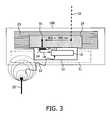
- FIG. 3shows a plurality of chip sensors 11 with a photosensor 14 .
- the filter materialconsists of the card material 23 and of a matrix 24 adjoining the card material 23 , which matrix generates modulated luminescences, in which a pulsed laser beam 22 first penetrates through the card material 23 and then penetrates the matrix 24 .
- the card material 23is adjusted in such a way that it completely absorbs light at wavelengths of less than 850 nm and is transparent at wavelengths of more than 850 nm in the NIR range.
- both energy 13 and informationis coupled into and stored on the chip 10 via an antenna 20 and an antenna periphery 21 so as to generate the RFID signal.
- the pulsed laser beam 22irradiates the matrix 24 with an emission at 980 nm, while a UP conversion process generates a luminescence at 800 nm (670, 550 or 430 nm).
- This in situ generated light(luminescence emission 31 ) is incident on the photosensor 14 and after excitation 12 triggers a signal 18 in the form of an exception signal, i.e.
- the luminescence dynamics of the UP conversion materialsshould be chosen to be such that the modulation of the pulsed laser beam 22 can be “passed on” so that a modulated luminescence reaches the photosensor 14 and complex optical information can thus be coupled in.
- a simple continuous excitation of the photosensor 14for example, the customary exception routine, deactivates the chip.
- a defined pulsed excitationtriggers other routines which lead to complex operations in the CPU 19 .
- the CPU 19is programmed in such a way that it does not only expect the “customary” RFID signal but also defined exception signals from the photosensor 14 so as to reach a complex result during the processing operation.
- the matrix 24may be formed with special material (combinations) so that, for example, other optical conversion processes such as photoluminescence or invisible Stokes luminescence can be utilized.
- the matrix 24may also be applied prior to laminating the compound material of the card by means of known printing techniques such as silkscreen printing, rotogravure, flexoprinting, offset, letter set, ink jet, thermotransfer etc. or the UC pigment may be incorporated when housing the chip in the epoxy resin substance so that only a pulsed laser beam 22 is suitable and the intensity of pulsed “NIR light” is not sufficient to generate adequate luminescences.
- the chip sensors 11 shown on an explicitly larger scale in FIG. 4communicate with filter material which consists of card material 23 which is opaque at wavelengths of less than 800 nm and transparent at wavelengths between 800 and 1100 nm, and of a UC converter 25 adjoining the card material 23 , as well as of an interference filter laminate 27 adjoining the UC converter, in which the pulsed laser beam 22 penetrates through the card material 23 and penetrates the UC converter 25 .
- the UC converter 25which is printed on the rear side of the card material 23 consists of, for example, ytterbium and holmium-doped gadolinium oxysulphide as a phosphor and is favorably formed in such a way that the UC radiation 26 is essentially directed downwards in the direction of the photosensor 14 in the form of a Si photosensor and is used as excitation.
- the interference filter laminate 27has very sharp absorption edges so as to absorb light of wavelengths between 800 and 1100 nm. Due to the phosphors used, the UC converter generates an emission at 550 nm. The luminescence can only spread in the direction of the Si photosensor where it triggers a signal 18 which is passed on to the CPU 19 . However, the laser beam required for excitation would be absorbed in the filter laminate layer at the latest and could thus not activate the Si photosensor.
- FIG. 5shows a plurality of chip sensors 11 including a photosensor 14 in the form of a Si photosensor, with filter material consisting of a light converter 28 shifting wavelengths and card material 23 adjoining the light converter 28 , which is transparent in a wavelength range between 800 and 1100 nm, and in which a pulsed laser beam 22 penetrates the light converter 28 .
- the light converter 28consists of (chromium) lanthanoide-doped yttrium vanadates (yttrium phosphates, yttrium borates) absorbing red light and generating an emission in the NIR range. The original excitation light is thus shifted as a long wave.
- the light converteris printed by means of a conventional printing method or put in front as a foil additive.
- Other materialssuch as, for example, chromium and neodymium-doped yttrium aluminum garnets defined by the general formula YAG:Cr,Nd can also be used as light converters.
- the card material 23 adjoining the light converter 28is only transparent in the NIR range of 800 to 1100 nm.
- the light converter 28absorbs a pulsed laser beam 22 between 800 and 1100 nm substantially completely so that the pulsed laser does not reach the photosensor 14 .
- red laser light(630-690 nm) triggers a luminescence 29 between 900 and 1000 nm dependent on the design of the light converter 28 , which luminescence reaches the photosensor 14 through the card material 23 and serves as excitation for the photosensor 14 , further reaching the CPU 19 as signal 18 .
- Dependent on the light clockfor example, exceptions or defined warm resets are performed which are then treated as information by the operating system of the CPU 19 .
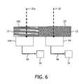
- the plurality of chip sensors shown in FIG. 6includes at least two photosensors 14 , 14 a whose filter material is different, the filter material consisting of card material 23 , in which a pulsed laser beam 22 , 22 a penetrates through the filter material and excites the photosensors 14 , 14 a which separately pass on a signal 18 to the CPU 19 .
- the photosensors 14 , 14 aare sensitized for different wavelengths.
- the card material 23 ais doped with an ytterbium phosphate and formed in such a way that it is transparent at wavelengths of less than 800 nm and substantially opaque at wavelengths of more than 800 nm.
- a photosensor 14 adetects the excitation 12 of a pulsed laser beam 22 a (wavelength 650 nm) and converts it into a signal 18 for the CPU 19 , which signal is utilized to enable the second photosensor which can now detect the excitation 12 of a pulsed laser beam 22 at a wavelength of 980 nm. In this way, information is divided between different photosensors 14 , 14 a , with the result that a ternary logic can be implemented.
Landscapes
- Engineering & Computer Science (AREA)
- Computer Hardware Design (AREA)
- Physics & Mathematics (AREA)
- General Physics & Mathematics (AREA)
- Theoretical Computer Science (AREA)
- Microelectronics & Electronic Packaging (AREA)
- Computer Networks & Wireless Communication (AREA)
- General Engineering & Computer Science (AREA)
- Computer Security & Cryptography (AREA)
- Electromagnetism (AREA)
- Computer Vision & Pattern Recognition (AREA)
- Artificial Intelligence (AREA)
- Toxicology (AREA)
- General Health & Medical Sciences (AREA)
- Health & Medical Sciences (AREA)
- Credit Cards Or The Like (AREA)
- Investigating, Analyzing Materials By Fluorescence Or Luminescence (AREA)
- Near-Field Transmission Systems (AREA)
- Radar Systems Or Details Thereof (AREA)
Abstract
Description
- 100 data carrier
- 10 chip
- 11 plurality of chip sensors
- 12 excitation
- 13 energy
- 14 photosensor
- 14aphotosensor
- 15 temperature sensor
- 16 frequency sensor
- 17 sensor
- 18 signal
- 19 CPU
- 20 antenna
- 21 antenna periphery
- 22 pulsed laser beam
- 22apulsed laser beam
- 23 card material
- 23aytterbium phosphate card material
- 24 matrix
- 25 UC converter
- 26 UC radiation
- 27 interference filter laminate
- 28 light converter
- 29 luminescence
- 30 electromagnetic field
- 31 luminescence emission
Claims (4)
Applications Claiming Priority (4)
| Application Number | Priority Date | Filing Date | Title |
|---|---|---|---|
| EP04106463.5 | 2004-12-10 | ||
| EP04106463 | 2004-12-10 | ||
| EP04106463 | 2004-12-10 | ||
| PCT/IB2005/054081WO2006061780A1 (en) | 2004-12-10 | 2005-12-06 | Data carrier with a chip and a plurality of sensors |
Publications (2)
| Publication Number | Publication Date |
|---|---|
| US20090294535A1 US20090294535A1 (en) | 2009-12-03 |
| US8899486B2true US8899486B2 (en) | 2014-12-02 |
Family
ID=36087732
Family Applications (1)
| Application Number | Title | Priority Date | Filing Date |
|---|---|---|---|
| US11/721,433Active2030-06-15US8899486B2 (en) | 2004-12-10 | 2005-12-06 | Data carrier with a chip and a plurality of sensors |
Country Status (8)
| Country | Link |
|---|---|
| US (1) | US8899486B2 (en) |
| EP (1) | EP1866845B1 (en) |
| CN (1) | CN101116092B (en) |
| BR (1) | BRPI0518880A2 (en) |
| CA (1) | CA2590150C (en) |
| MX (1) | MX2007006741A (en) |
| PL (1) | PL1866845T3 (en) |
| WO (1) | WO2006061780A1 (en) |
Families Citing this family (12)
| Publication number | Priority date | Publication date | Assignee | Title |
|---|---|---|---|---|
| US20150191037A1 (en) | 2007-12-07 | 2015-07-09 | Bundesdruckerei Gmbh | Method for producing a security and/or valuable document with personalized information |
| DE102008001149B4 (en) | 2008-04-14 | 2024-09-26 | Bundesdruckerei Gmbh | Document with a memory and receiver device |
| DE102008041306A1 (en) | 2008-08-18 | 2010-02-25 | Bundesdruckerei Gmbh | Document and method for the self-verification of a document |
| US8205800B2 (en)* | 2009-10-20 | 2012-06-26 | Hand Held Products, Inc. | Long range selective RFID using laser photodetection wakeup |
| EP2343174A1 (en)* | 2010-01-11 | 2011-07-13 | Gemalto SA | Moulded smart cards and manufacturing method |
| DE102010020460B4 (en) | 2010-05-11 | 2023-12-21 | Bundesdruckerei Gmbh | Security or value document, process for its production and its verification |
| US9937124B2 (en) | 2014-09-11 | 2018-04-10 | International Business Machines Corporation | Microchip substance delivery devices having low-power electromechanical release mechanisms |
| US9734371B2 (en)* | 2015-03-31 | 2017-08-15 | International Business Machines Corporation | Hybrid tag for radio frequency identification system |
| US10881788B2 (en) | 2015-10-30 | 2021-01-05 | International Business Machines Corporation | Delivery device including reactive material for programmable discrete delivery of a substance |
| DE102016104867B4 (en)* | 2016-03-16 | 2021-06-02 | Bundesdruckerei Gmbh | Authentication document |
| WO2019008159A1 (en) | 2017-07-06 | 2019-01-10 | Fraunhofer-Gesellschaft zur Förderung der angewandten Forschung e.V. | DEVICE AND METHOD FOR FALTER-PROTECTION OF A PRODUCT |
| US20200387765A1 (en)* | 2018-02-23 | 2020-12-10 | Equinox Card Ltd. | Security Measures in Relation to Data Tags and Contactless Cards |
Citations (32)
| Publication number | Priority date | Publication date | Assignee | Title |
|---|---|---|---|---|
| US3426212A (en)* | 1968-03-14 | 1969-02-04 | Ruth Elizabeth Barry Klaas | Radiation converter comprising transparent parallel layers containing fluorescent substances |
| US5825045A (en)* | 1992-02-13 | 1998-10-20 | Norand Corporation | Extended range highly selective low power consuming data tag and information display system |
| US5874724A (en) | 1997-01-10 | 1999-02-23 | International Business Machines Corporation | Light selectable radio frequency identification tag and method therefor |
| US6294997B1 (en) | 1999-10-04 | 2001-09-25 | Intermec Ip Corp. | RFID tag having timing and environment modules |
| US20020031838A1 (en) | 2000-07-28 | 2002-03-14 | Meinhart Carl D. | Integrated sensor |
| US20020127481A1 (en)* | 2001-03-07 | 2002-09-12 | Jain-Hon Chen | Method of forming color filter array |
| US20020186145A1 (en) | 1999-01-11 | 2002-12-12 | Timothy J. Chainer | Method and apparatus for securely determining aspects of the history of a good |
| US20040012496A1 (en) | 2002-07-17 | 2004-01-22 | Ncr Corporation | Radio frequency identification (RFID) tag and a method of operating an RFID tag |
| US20040052203A1 (en) | 2002-09-13 | 2004-03-18 | Brollier Brian W. | Light enabled RFID in information disks |
| US20040062294A1 (en) | 2000-12-08 | 2004-04-01 | Wolfgang Clemens | Device for detecting and/or transmitting at least one environmental influence, method for producing said device and use thereof |
| US20040100834A1 (en) | 2002-11-21 | 2004-05-27 | Hewlett-Packard Development Company, L.P. | Memory tag, read/write device and method of operating a memory tag |
| US20040181516A1 (en)* | 2003-03-13 | 2004-09-16 | First Data Corporation | Methods and systems for monitoring document-production processes |
| US6802008B1 (en)* | 1997-05-19 | 2004-10-05 | Rohm Co., Ltd. | IC card and IC chip module |
| US20040246099A1 (en)* | 1992-08-12 | 2004-12-09 | Micron Technology, Inc. | Miniature radio frequency transceiver |
| US20050040241A1 (en)* | 2003-08-19 | 2005-02-24 | Ramesh Raskar | Radio and optical identification tags |
| US20050116813A1 (en)* | 2003-08-19 | 2005-06-02 | Ramesh Raskar | Radio and optical identification tags |
| US20050163511A1 (en)* | 2004-01-27 | 2005-07-28 | Cicchiello James M. | Dynamic optical tag |
| US20060033325A1 (en)* | 2004-07-13 | 2006-02-16 | Sriramakrishna Maruvada | Authenticatable article and method of authenticating |
| US20060114377A1 (en)* | 2004-11-30 | 2006-06-01 | Toppoly Optoelectronics Corp. | Color filter process |
| US20060164291A1 (en)* | 2003-03-10 | 2006-07-27 | Staffan Gunnarsson | System for identification using a transponder powered by solar cells |
| US7154395B2 (en)* | 2004-07-01 | 2006-12-26 | Mitsubishi Electric Research Laboratories, Inc. | Interactive wireless tag location and identification system |
| US20070040683A1 (en)* | 2005-08-22 | 2007-02-22 | Neal Oliver | Light-activated RFID tag |
| US20070222591A1 (en)* | 2006-03-27 | 2007-09-27 | Nec Corporation | Information management system, method, program and recording medium |
| US7425899B2 (en)* | 2005-12-08 | 2008-09-16 | Palo Alto Research Center Incorporated | Electromagnetic tags |
| US20090009288A1 (en)* | 2004-01-15 | 2009-01-08 | Zih Corp. | Radio Frequency Identification Tagging |
| US20090051497A1 (en)* | 2006-03-09 | 2009-02-26 | Matsushita Electric Industrial Co., Ltd. | Wireless ic tag, document medium, and information processor |
| US7652557B2 (en)* | 2004-02-13 | 2010-01-26 | Kantrowitz Allen B | Optical transponder containing identification tag |
| US7671721B2 (en)* | 2003-05-12 | 2010-03-02 | Valtion Teknillinen Tutkimuskesus | Remote sensor, device and method for activating selected remote sensor components |
| US7791481B2 (en)* | 2007-01-22 | 2010-09-07 | Tc License Ltd. | Light activated RFID tag |
| US7813175B2 (en)* | 2006-12-06 | 2010-10-12 | Samsung Electronics Co., Ltd. | Smart card capable of sensing light |
| US20110091216A1 (en)* | 2009-10-20 | 2011-04-21 | Ken Addy | Long range selective rfid using laser photodetection wakeup |
| US20120000985A1 (en)* | 2007-07-30 | 2012-01-05 | Lasercard Corporation | Light enabled rfid card |
Family Cites Families (1)
| Publication number | Priority date | Publication date | Assignee | Title |
|---|---|---|---|---|
| CN2266159Y (en)* | 1996-12-24 | 1997-10-29 | 中国科学院上海技术物理研究所 | Infrared non-contact type intelligent card |
- 2005
- 2005-12-06MXMX2007006741Apatent/MX2007006741A/enactiveIP Right Grant
- 2005-12-06WOPCT/IB2005/054081patent/WO2006061780A1/enactiveApplication Filing
- 2005-12-06BRBRPI0518880-6Apatent/BRPI0518880A2/ennot_activeApplication Discontinuation
- 2005-12-06CNCN2005800479176Apatent/CN101116092B/enactiveActive
- 2005-12-06CACA2590150Apatent/CA2590150C/enactiveActive
- 2005-12-06USUS11/721,433patent/US8899486B2/enactiveActive
- 2005-12-06EPEP05822517Apatent/EP1866845B1/enactiveActive
- 2005-12-06PLPL05822517Tpatent/PL1866845T3/enunknown
Patent Citations (32)
| Publication number | Priority date | Publication date | Assignee | Title |
|---|---|---|---|---|
| US3426212A (en)* | 1968-03-14 | 1969-02-04 | Ruth Elizabeth Barry Klaas | Radiation converter comprising transparent parallel layers containing fluorescent substances |
| US5825045A (en)* | 1992-02-13 | 1998-10-20 | Norand Corporation | Extended range highly selective low power consuming data tag and information display system |
| US20040246099A1 (en)* | 1992-08-12 | 2004-12-09 | Micron Technology, Inc. | Miniature radio frequency transceiver |
| US5874724A (en) | 1997-01-10 | 1999-02-23 | International Business Machines Corporation | Light selectable radio frequency identification tag and method therefor |
| US6802008B1 (en)* | 1997-05-19 | 2004-10-05 | Rohm Co., Ltd. | IC card and IC chip module |
| US20020186145A1 (en) | 1999-01-11 | 2002-12-12 | Timothy J. Chainer | Method and apparatus for securely determining aspects of the history of a good |
| US6294997B1 (en) | 1999-10-04 | 2001-09-25 | Intermec Ip Corp. | RFID tag having timing and environment modules |
| US20020031838A1 (en) | 2000-07-28 | 2002-03-14 | Meinhart Carl D. | Integrated sensor |
| US20040062294A1 (en) | 2000-12-08 | 2004-04-01 | Wolfgang Clemens | Device for detecting and/or transmitting at least one environmental influence, method for producing said device and use thereof |
| US20020127481A1 (en)* | 2001-03-07 | 2002-09-12 | Jain-Hon Chen | Method of forming color filter array |
| US20040012496A1 (en) | 2002-07-17 | 2004-01-22 | Ncr Corporation | Radio frequency identification (RFID) tag and a method of operating an RFID tag |
| US20040052203A1 (en) | 2002-09-13 | 2004-03-18 | Brollier Brian W. | Light enabled RFID in information disks |
| US20040100834A1 (en) | 2002-11-21 | 2004-05-27 | Hewlett-Packard Development Company, L.P. | Memory tag, read/write device and method of operating a memory tag |
| US20060164291A1 (en)* | 2003-03-10 | 2006-07-27 | Staffan Gunnarsson | System for identification using a transponder powered by solar cells |
| US20040181516A1 (en)* | 2003-03-13 | 2004-09-16 | First Data Corporation | Methods and systems for monitoring document-production processes |
| US7671721B2 (en)* | 2003-05-12 | 2010-03-02 | Valtion Teknillinen Tutkimuskesus | Remote sensor, device and method for activating selected remote sensor components |
| US20050040241A1 (en)* | 2003-08-19 | 2005-02-24 | Ramesh Raskar | Radio and optical identification tags |
| US20050116813A1 (en)* | 2003-08-19 | 2005-06-02 | Ramesh Raskar | Radio and optical identification tags |
| US20090009288A1 (en)* | 2004-01-15 | 2009-01-08 | Zih Corp. | Radio Frequency Identification Tagging |
| US20050163511A1 (en)* | 2004-01-27 | 2005-07-28 | Cicchiello James M. | Dynamic optical tag |
| US7652557B2 (en)* | 2004-02-13 | 2010-01-26 | Kantrowitz Allen B | Optical transponder containing identification tag |
| US7154395B2 (en)* | 2004-07-01 | 2006-12-26 | Mitsubishi Electric Research Laboratories, Inc. | Interactive wireless tag location and identification system |
| US20060033325A1 (en)* | 2004-07-13 | 2006-02-16 | Sriramakrishna Maruvada | Authenticatable article and method of authenticating |
| US20060114377A1 (en)* | 2004-11-30 | 2006-06-01 | Toppoly Optoelectronics Corp. | Color filter process |
| US20070040683A1 (en)* | 2005-08-22 | 2007-02-22 | Neal Oliver | Light-activated RFID tag |
| US7425899B2 (en)* | 2005-12-08 | 2008-09-16 | Palo Alto Research Center Incorporated | Electromagnetic tags |
| US20090051497A1 (en)* | 2006-03-09 | 2009-02-26 | Matsushita Electric Industrial Co., Ltd. | Wireless ic tag, document medium, and information processor |
| US20070222591A1 (en)* | 2006-03-27 | 2007-09-27 | Nec Corporation | Information management system, method, program and recording medium |
| US7813175B2 (en)* | 2006-12-06 | 2010-10-12 | Samsung Electronics Co., Ltd. | Smart card capable of sensing light |
| US7791481B2 (en)* | 2007-01-22 | 2010-09-07 | Tc License Ltd. | Light activated RFID tag |
| US20120000985A1 (en)* | 2007-07-30 | 2012-01-05 | Lasercard Corporation | Light enabled rfid card |
| US20110091216A1 (en)* | 2009-10-20 | 2011-04-21 | Ken Addy | Long range selective rfid using laser photodetection wakeup |
Non-Patent Citations (3)
| Title |
|---|
| "Filter." The Photonics Dictionary, 45th ed. 1999.* |
| Britton, C.L; et al "Battery-Powered, Wireless MEMS Sensors for High-Sensitivity Chemical and Biological Sensing" Oak Ridge National Laboratory, The University of Tennessee, Knoxville 2002. |
| Y. Haghiri/Th. Tarantino, "Vom Plastik zur Chipkarte" ("From plastic to chip card"), Carl Hanser Publishers, Munich, Vienna, 1999; Chapter (2): "Kartenkorper" (Card bodies) and Chapter (3): "Herstellungsformen fur Kartenkorper" ("Methods of manufacturing card bodies"). |
Also Published As
| Publication number | Publication date |
|---|---|
| CN101116092A (en) | 2008-01-30 |
| BRPI0518880A2 (en) | 2008-12-16 |
| EP1866845B1 (en) | 2013-03-27 |
| CA2590150C (en) | 2013-05-14 |
| CA2590150A1 (en) | 2006-06-15 |
| MX2007006741A (en) | 2007-11-23 |
| CN101116092B (en) | 2011-02-16 |
| PL1866845T3 (en) | 2013-08-30 |
| US20090294535A1 (en) | 2009-12-03 |
| WO2006061780A1 (en) | 2006-06-15 |
| EP1866845A1 (en) | 2007-12-19 |
Similar Documents
| Publication | Publication Date | Title |
|---|---|---|
| US8899486B2 (en) | Data carrier with a chip and a plurality of sensors | |
| US11879083B2 (en) | Multi-luminescent security element and value or security product containing said security element | |
| US11949768B2 (en) | Light-triggered transponder | |
| EP4112327B1 (en) | Laminates and identification documents | |
| KR101432856B1 (en) | Document with optical transmitter | |
| KR100697844B1 (en) | RFID card using Korean paper and its manufacturing method | |
| CN107408216B (en) | Value or security document having an electronic circuit and method for producing a value or security document | |
| US20070257797A1 (en) | Structure Including an Electronic Device, in Particular for Fabricating a Security Document or a Document of Value | |
| EP3526054B1 (en) | Security document with a securing element and a method for producing thereof | |
| US10133976B2 (en) | Substrate | |
| WO2010071137A1 (en) | Optical reading method | |
| EP1431062B1 (en) | Security document comprising electronic security means | |
| US20080314988A1 (en) | Smart information carrier and production process therfor | |
| JP2009059304A (en) | Method for communicating with chip of information storage device and information storage device | |
| KR102780934B1 (en) | Optical trigger transponder | |
| US7479870B2 (en) | Method and apparatus for programming a transponder | |
| US20210379917A1 (en) | Drop-on-demand multi-pass printing on plastic cards | |
| EP4590519A1 (en) | Data carrier with independent light source and method of producing it | |
| JP2022057970A (en) | Laminated body and laminated body issuing system and laminated body issuing method | |
| HK1248016A1 (en) | Structure comprising an electronic device, in particular for manufacturing a security or value document | |
| JP2006235768A (en) | Ic chip incorporated supporting body |
Legal Events
| Date | Code | Title | Description |
|---|---|---|---|
| AS | Assignment | Owner name:KONINKLIJKE PHILIPS ELECTRONICS N.V., NETHERLANDS Free format text:ASSIGNMENT OF ASSIGNORS INTEREST;ASSIGNORS:PAESCHKE, MANFRED;NGUYEN, KIM;MUTH, OLIVER;AND OTHERS;SIGNING DATES FROM 20070614 TO 20070705;REEL/FRAME:022821/0773 | |
| AS | Assignment | Owner name:NXP B.V.,NETHERLANDS Free format text:DEED OF TRANSFER OF PATENTS;ASSIGNOR:KONINKLIJKE PHILIPS ELECTRONICS N.V.;REEL/FRAME:023571/0580 Effective date:20091119 Owner name:NXP B.V., NETHERLANDS Free format text:DEED OF TRANSFER OF PATENTS;ASSIGNOR:KONINKLIJKE PHILIPS ELECTRONICS N.V.;REEL/FRAME:023571/0580 Effective date:20091119 | |
| FEPP | Fee payment procedure | Free format text:PAYOR NUMBER ASSIGNED (ORIGINAL EVENT CODE: ASPN); ENTITY STATUS OF PATENT OWNER: LARGE ENTITY | |
| AS | Assignment | Owner name:QUOTAINNE ENTERPRISES LLC, DELAWARE Free format text:ASSIGNMENT OF ASSIGNORS INTEREST;ASSIGNOR:NXP, B.V.;REEL/FRAME:032842/0964 Effective date:20131216 | |
| AS | Assignment | Owner name:QUOTAINNE ENTERPRISES LLC, DELAWARE Free format text:CORRECTIVE ASSIGNMENT TO CORRECT THE ERRONEOUSLY ADDED PROPERTY NUMBER: 12/555,651 BY EXCLUDING IT FROM THE PROPERTY LIST PREVIOUSLY RECORDED ON REEL 032842 FRAME 0964. ASSIGNOR(S) HEREBY CONFIRMS THE UPDATED PROPERTY LIST OF THE ASSIGNMENT;ASSIGNOR:NXP, B.V.;REEL/FRAME:033726/0436 Effective date:20131216 | |
| STCF | Information on status: patent grant | Free format text:PATENTED CASE | |
| MAFP | Maintenance fee payment | Free format text:PAYMENT OF MAINTENANCE FEE, 4TH YEAR, LARGE ENTITY (ORIGINAL EVENT CODE: M1551) Year of fee payment:4 | |
| MAFP | Maintenance fee payment | Free format text:PAYMENT OF MAINTENANCE FEE, 8TH YEAR, LARGE ENTITY (ORIGINAL EVENT CODE: M1552); ENTITY STATUS OF PATENT OWNER: LARGE ENTITY Year of fee payment:8 |