US8895339B2 - Reducing MEMS stiction by introduction of a carbon barrier - Google Patents
Reducing MEMS stiction by introduction of a carbon barrierDownload PDFInfo
- Publication number
- US8895339B2 US8895339B2US13/718,598US201213718598AUS8895339B2US 8895339 B2US8895339 B2US 8895339B2US 201213718598 AUS201213718598 AUS 201213718598AUS 8895339 B2US8895339 B2US 8895339B2
- Authority
- US
- United States
- Prior art keywords
- layer
- polysilicon
- forming
- carbon
- barrier layer
- Prior art date
- Legal status (The legal status is an assumption and is not a legal conclusion. Google has not performed a legal analysis and makes no representation as to the accuracy of the status listed.)
- Active
Links
Images


Classifications
- B—PERFORMING OPERATIONS; TRANSPORTING
- B81—MICROSTRUCTURAL TECHNOLOGY
- B81B—MICROSTRUCTURAL DEVICES OR SYSTEMS, e.g. MICROMECHANICAL DEVICES
- B81B3/00—Devices comprising flexible or deformable elements, e.g. comprising elastic tongues or membranes
- B81B3/0002—Arrangements for avoiding sticking of the flexible or moving parts
- B81B3/0005—Anti-stiction coatings
- B—PERFORMING OPERATIONS; TRANSPORTING
- B81—MICROSTRUCTURAL TECHNOLOGY
- B81C—PROCESSES OR APPARATUS SPECIALLY ADAPTED FOR THE MANUFACTURE OR TREATMENT OF MICROSTRUCTURAL DEVICES OR SYSTEMS
- B81C1/00—Manufacture or treatment of devices or systems in or on a substrate
- B81C1/00349—Creating layers of material on a substrate
- B81C1/0038—Processes for creating layers of materials not provided for in groups B81C1/00357 - B81C1/00373
- B—PERFORMING OPERATIONS; TRANSPORTING
- B81—MICROSTRUCTURAL TECHNOLOGY
- B81C—PROCESSES OR APPARATUS SPECIALLY ADAPTED FOR THE MANUFACTURE OR TREATMENT OF MICROSTRUCTURAL DEVICES OR SYSTEMS
- B81C1/00—Manufacture or treatment of devices or systems in or on a substrate
- B81C1/00912—Treatments or methods for avoiding stiction of flexible or moving parts of MEMS
- B81C1/0092—For avoiding stiction during the manufacturing process of the device, e.g. during wet etching
- B81C1/00952—Treatments or methods for avoiding stiction during the manufacturing process not provided for in groups B81C1/00928 - B81C1/00944
- G—PHYSICS
- G01—MEASURING; TESTING
- G01P—MEASURING LINEAR OR ANGULAR SPEED, ACCELERATION, DECELERATION, OR SHOCK; INDICATING PRESENCE, ABSENCE, OR DIRECTION, OF MOVEMENT
- G01P15/00—Measuring acceleration; Measuring deceleration; Measuring shock, i.e. sudden change of acceleration
- G01P15/02—Measuring acceleration; Measuring deceleration; Measuring shock, i.e. sudden change of acceleration by making use of inertia forces using solid seismic masses
- G01P15/08—Measuring acceleration; Measuring deceleration; Measuring shock, i.e. sudden change of acceleration by making use of inertia forces using solid seismic masses with conversion into electric or magnetic values
- G01P15/0802—Details
- B—PERFORMING OPERATIONS; TRANSPORTING
- B81—MICROSTRUCTURAL TECHNOLOGY
- B81B—MICROSTRUCTURAL DEVICES OR SYSTEMS, e.g. MICROMECHANICAL DEVICES
- B81B2201/00—Specific applications of microelectromechanical systems
- B81B2201/02—Sensors
- B81B2201/0221—Variable capacitors
- B—PERFORMING OPERATIONS; TRANSPORTING
- B81—MICROSTRUCTURAL TECHNOLOGY
- B81B—MICROSTRUCTURAL DEVICES OR SYSTEMS, e.g. MICROMECHANICAL DEVICES
- B81B2201/00—Specific applications of microelectromechanical systems
- B81B2201/02—Sensors
- B81B2201/0228—Inertial sensors
- B81B2201/0235—Accelerometers
- B—PERFORMING OPERATIONS; TRANSPORTING
- B81—MICROSTRUCTURAL TECHNOLOGY
- B81B—MICROSTRUCTURAL DEVICES OR SYSTEMS, e.g. MICROMECHANICAL DEVICES
- B81B2203/00—Basic microelectromechanical structures
- B81B2203/01—Suspended structures, i.e. structures allowing a movement
- B81B2203/0181—See-saws
- B—PERFORMING OPERATIONS; TRANSPORTING
- B81—MICROSTRUCTURAL TECHNOLOGY
- B81B—MICROSTRUCTURAL DEVICES OR SYSTEMS, e.g. MICROMECHANICAL DEVICES
- B81B2203/00—Basic microelectromechanical structures
- B81B2203/06—Devices comprising elements which are movable in relation to each other, e.g. slidable or rotatable
- B—PERFORMING OPERATIONS; TRANSPORTING
- B81—MICROSTRUCTURAL TECHNOLOGY
- B81C—PROCESSES OR APPARATUS SPECIALLY ADAPTED FOR THE MANUFACTURE OR TREATMENT OF MICROSTRUCTURAL DEVICES OR SYSTEMS
- B81C2201/00—Manufacture or treatment of microstructural devices or systems
- B81C2201/01—Manufacture or treatment of microstructural devices or systems in or on a substrate
- B81C2201/0161—Controlling physical properties of the material
- B81C2201/0163—Controlling internal stress of deposited layers
- B81C2201/0169—Controlling internal stress of deposited layers by post-annealing
- B—PERFORMING OPERATIONS; TRANSPORTING
- B81—MICROSTRUCTURAL TECHNOLOGY
- B81C—PROCESSES OR APPARATUS SPECIALLY ADAPTED FOR THE MANUFACTURE OR TREATMENT OF MICROSTRUCTURAL DEVICES OR SYSTEMS
- B81C2201/00—Manufacture or treatment of microstructural devices or systems
- B81C2201/11—Treatments for avoiding stiction of elastic or moving parts of MEMS
- B81C2201/112—Depositing an anti-stiction or passivation coating, e.g. on the elastic or moving parts
- G—PHYSICS
- G01—MEASURING; TESTING
- G01P—MEASURING LINEAR OR ANGULAR SPEED, ACCELERATION, DECELERATION, OR SHOCK; INDICATING PRESENCE, ABSENCE, OR DIRECTION, OF MOVEMENT
- G01P15/00—Measuring acceleration; Measuring deceleration; Measuring shock, i.e. sudden change of acceleration
- G01P15/02—Measuring acceleration; Measuring deceleration; Measuring shock, i.e. sudden change of acceleration by making use of inertia forces using solid seismic masses
- G01P15/08—Measuring acceleration; Measuring deceleration; Measuring shock, i.e. sudden change of acceleration by making use of inertia forces using solid seismic masses with conversion into electric or magnetic values
- G01P2015/0862—Measuring acceleration; Measuring deceleration; Measuring shock, i.e. sudden change of acceleration by making use of inertia forces using solid seismic masses with conversion into electric or magnetic values being provided with particular means being integrated into a MEMS accelerometer structure for providing particular additional functionalities to those of a spring mass system
- G01P2015/0871—Measuring acceleration; Measuring deceleration; Measuring shock, i.e. sudden change of acceleration by making use of inertia forces using solid seismic masses with conversion into electric or magnetic values being provided with particular means being integrated into a MEMS accelerometer structure for providing particular additional functionalities to those of a spring mass system using stopper structures for limiting the travel of the seismic mass
- G—PHYSICS
- G01—MEASURING; TESTING
- G01P—MEASURING LINEAR OR ANGULAR SPEED, ACCELERATION, DECELERATION, OR SHOCK; INDICATING PRESENCE, ABSENCE, OR DIRECTION, OF MOVEMENT
- G01P15/00—Measuring acceleration; Measuring deceleration; Measuring shock, i.e. sudden change of acceleration
- G01P15/02—Measuring acceleration; Measuring deceleration; Measuring shock, i.e. sudden change of acceleration by making use of inertia forces using solid seismic masses
- G01P15/08—Measuring acceleration; Measuring deceleration; Measuring shock, i.e. sudden change of acceleration by making use of inertia forces using solid seismic masses with conversion into electric or magnetic values
- G01P2015/0862—Measuring acceleration; Measuring deceleration; Measuring shock, i.e. sudden change of acceleration by making use of inertia forces using solid seismic masses with conversion into electric or magnetic values being provided with particular means being integrated into a MEMS accelerometer structure for providing particular additional functionalities to those of a spring mass system
- G01P2015/0874—Measuring acceleration; Measuring deceleration; Measuring shock, i.e. sudden change of acceleration by making use of inertia forces using solid seismic masses with conversion into electric or magnetic values being provided with particular means being integrated into a MEMS accelerometer structure for providing particular additional functionalities to those of a spring mass system using means for preventing stiction of the seismic mass to the substrate
Definitions
- This disclosurerelates generally to manufacture of microelectromechanical systems (MEMS), and more specifically, to reducing stiction in MEMS devices through the use of a carbon barrier layer during formation of the MEMS device.
- MEMSmicroelectromechanical systems
- MEMS devicesare micromechanical devices that provide moving parts having features with dimensions below 100 ⁇ m. These moving parts are formed using micro-fabrication techniques. MEMS devices have holes, cavities, channels, cantilevers, membranes, and the like. These devices are typically based on silicon materials and use a variety of techniques to form the physical structures and to free the structures for movement.
- Stictionis a static friction force that is a recurring problem with typical MEMS devices. While any solid objects pressing against each other without sliding require some threshold of force (stiction) to overcome static cohesion, the mechanisms generating this force can be different for MEMS devices. When two surfaces with areas below the micrometer range come into close proximity, the surfaces may adhere together due to electrostatic and/or Van der Waals forces. Stiction forces at this scale may also be related to hydrogen bonding or residual contamination on the surfaces.
- MEMS devicessuch as accelerometers
- surfacessuch as over-travel stops can come into close proximity or contact during use at the limits of the device design or during manufacture of the device.
- stiction forcescan cause the MEMS device parts (e.g., a teeter-totter accelerometer mechanism) to freeze in place and become unusable.
- Traditional methods of avoiding such close proximity travel or contactinclude increasing spring constants and increasing distance between parts of the MEMS device. But these methods can cause decreased sensitivity of the device to acceleration, and therefore decreased utility of the MEMS device. It is therefore desirable to provide a mechanism for reducing stiction-related interactions of MEMS devices without also decreasing sensitivity of the MEMS device.
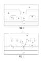
- FIG. 1is a simplified block diagram illustrating a cross section view of an accelerometer known in the art.
- FIG. 2is a simplified block diagram illustrating a close up of a cross-section view of the travel stop region at an end of a MEMS accelerometer during a stage of fabrication.
- FIG. 3is a simplified block diagram illustrating a cross-section view of the travel stop region during a stage of fabrication subsequent to deposition of a second polysilicon layer.
- FIG. 4is a simplified block diagram illustrating a cross-section view of the travel stop region subsequent to removal of a sacrificial layer, in a position that can occur during use of the accelerometer or during removal of the sacrificial layer.
- FIG. 5is a simplified block diagram illustrating a cross-sectional view of the travel stop region during a step in processing, in accord with embodiments of the present invention.
- FIGS. 6A , 6 B, 7 A, and 7 Bare example secondary ion mass spectrometry (SIMS) depth resolution profiles showing the effect upon carbon diffusion into the polysilicon layer by inclusion of a barrier layer, in accord with embodiments of the present invention.
- SIMSsecondary ion mass spectrometry
- Embodiments of the present inventionprovide a mechanism for reducing stiction in a MEMS device by decreasing an amount of carbon from TEOS-based silicon oxide films that can accumulate on polysilicon surfaces during fabrication.
- a carbon barrier material filmis deposited between one or more polysilicon layer in a MEMS device and the TEOS-based silicon oxide layer. This barrier material blocks diffusion of carbon into the polysilicon, thereby reducing accumulation of carbon on the polysilicon surfaces. By reducing the accumulation of carbon, the opportunity for stiction due to the presence of the carbon is similarly reduced.
- FIG. 1is a simplified block diagram illustrating a cross section view of a teeter totter accelerometer known in the prior art.
- the accelerometerincludes a substrate 110 with an insulating layer 120 .
- Substrate 110can be, for example, a silicon wafer and insulating layer 120 can be, for example, a silicon oxide or silicon nitride. In some cases, insulating layer 120 can be thermally grown from substrate 110 or the insulating layer can be deposited.
- Fixed electrodes 130 and 135are formed on top of insulating layer 120 , along with travel stop regions 140 and 145 .
- the layer forming fixed electrodes 130 and 135 and travel stop regions 140 and 145is typically polysilicon and is formed using conventional techniques, including patterning as desired for the application.
- the layer forming the fixed electrodes and travel stop regionscan alternatively be amorphous silicon, a nitride, a metal-containing material, another suitable material, and the like, or any combination thereof.
- a dielectric layer 150is formed to electrically isolate the electrodes and travel stop regions from other elements of the MEMS accelerometer.
- Dielectric layer 150can be formed from a variety of materials, including, for example, silicon nitride, silicon dioxide, silicon oxynitride, and the like.
- a pivoting proof mass 160is configured to move in a manner similar to that of a teeter totter in response to acceleration of the MEMS device or a system incorporating the MEMS device. Pivoting proof mass 160 can be configured in a manner such that there is an imbalance between a side 170 of the pivoting proof mass and side 175 of the pivoting proof mass through pivot point 165 . The amount of imbalance has an effect of making the device more or less sensitive to acceleration.
- An electrode 180 configured on side 170 of the pivoting proof massis associated with fixed electrode 130
- an electrode 185 on the pivoting proof massis associated with fixed electrode 135 .
- a travel stop 190 on side 170 of the pivoting proof massis associated with travel stop region 140 and a travel stop 195 on side 175 of the pivoting proof mass is associated with travel stop region 145 .
- Pivoting proof mass 160 and travel stops 190 and 195are typically formed of polysilicon.
- Electrode 180 and fixed electrode 130form a first variable sense capacitor, while electrode 185 and fixed electrode 135 form a second variable sense capacitor. Changes in the capacitances of the first and second variable sense capacitors can be combined to provide a differential output from the MEMS accelerometer. Fabrication of the MEMS accelerometer in FIG. 1 can be performed using known MEMS fabrication processes.
- FIG. 2is a simplified block diagram illustrating a close up of a cross section view of the travel stop region at end 175 of the MEMS accelerometer during a stage of fabrication.
- a substrate 110is provided with insulating layer 120 , where substrate 110 can be a silicon wafer and insulating layer 120 can be a silicon oxide.
- a first polysilicon layer 210is formed on insulating layer 120 , forming, in part, travel stop region 145 .
- Dielectric layer 150is formed over polysilicon layer 210 and insulating layer 120 , in order to prevent excessive etching of insulating layer 120 , for example.
- a sacrificial layer 220is formed on top of patterned dielectric layer 150 and exposed regions of polysilicon layer 210 .
- Sacrificial layer 220is commonly formed using tetraethyl orthosilicate (TEOS) gas to form a sacrificial layer of silicon oxide or the sacrificial layer can be formed of phosphosilicate glass (PSG).
- TEOStetraethyl orthosilicate
- PSGphosphosilicate glass
- the sacrificial layercan be patterned to form a “molding” for the next layer of the MEMS device.
- Sacrificial layer 220may be annealed at this time at elevated temperatures (e.g., in excess of 900 C).
- a second polysilicon layer 230can be formed on the patterned sacrificial layer to form pivoting proof mass 160 , including travel stop 195 . The buildup of patterned layers can continue as needed for the application.
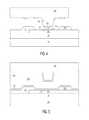
- FIG. 3is a simplified block diagram illustrating a cross-section view of the travel stop region during a stage of fabrication subsequent to deposition of second polysilicon layer 230 .
- Typical MEMS processingprovides for the second polysilicon layer to be deposited at low temperature and low pressure.
- the structurein order to relieve stresses on second polysilicon layer 230 , the structure is annealed by subjecting the structure to temperatures in excess of 1000 C for an hour or more. During this anneal, the polysilicon grains in polysilicon layer 230 realign and thereby reduce intrinsic stress, and will provide a low energy, relaxed polysilicon structure in the resulting device.
- sacrificial layer 220is typically a silicon oxide layer formed using TEOS gas.
- TEOSincludes a significant amount of carbon chains that get incorporated into the sacrificial layer.
- volatile compounds in the sacrificial layerare released from the layer, but carbon remains within the sacrificial layer.
- carbon in the sacrificial layer that is near the polysilicon layerscan diffuse into the surfaces of the polysilicon layers and form carbon deposits along the interface region between the polysilicon layers and the sacrificial layer (e.g., carbon deposits 310 , 315 , 320 , 325 , 330 , 335 , and 340 ).
- FIG. 4is a simplified block diagram illustrating a cross-section view of the travel stop region subsequent to removal of the sacrificial layer, in a position that can occur during use of the accelerometer or during removal of the sacrificial layer.
- Sacrificial layer 220is commonly removed using an isotropic wet etch process selective to the sacrificial layer. But capillary forces due to surface tension of the liquid used for the etching process between travel stop 195 and polysilicon travel stop region 145 can draw the surfaces together. As illustrated, a consequence of the surfaces being drawn together results in bringing carbon deposits 310 and 315 into contact.
- a carbon-coated surfacecan be significantly more susceptible to adhesion than a clear surface, especially if the carbon region is wet such as during a wet etching process.
- the carbon-coated surfacescan be brought into contact during use of the device. For example, an acceleration sufficient to exceed the design specification for the accelerometer is exerted upon the device. This causes travel stop 195 to impact polysilicon travel stop region 145 , thereby preventing contact of electrode 185 to fixed electrode 135 . In this case, stiction forces due to the carbon deposits, along with other sources of stiction (e.g., Van der Waals forces and electrostatic forces) can cause the parts to stay together and render the device inoperable.
- sources of stictione.g., Van der Waals forces and electrostatic forces
- Embodiments of the present inventionprovide a mechanism to reduce carbon deposition on the polysilicon surfaces of, for example, both travel stop 195 and travel stop region 145 in a MEMS device. This reduction in carbon deposition will consequently reduce stiction due to carbon deposits. This is accomplished by forming a carbon barrier layer between the TEOS-based sacrificial layer and the polysilicon layers of one or both of the pivoting proof mass and the fixed portion (e.g., the travel stop region).
- FIG. 5is a simplified block diagram illustrating a cross-sectional view of the travel stop region of a MEMS device during a step in processing, in accord with embodiments of the present invention.
- the travel stop regionis formed over substrate 110 and insulating layer 120 .
- First polysilicon layer 210is formed over insulating layer 120 , forming, in part, travel stop region 145 .
- Dielectric layer 150is formed over patterned polysilicon layer 210 , again to electrically isolate patterned regions of the polysilicon layer.
- a first barrier layer 510is formed over first polysilicon layer 210 and dielectric layer 150 .
- First barrier layer 510prevents diffusion of carbon from a sacrificial layer into the surface of first polysilicon layer 210 , and therefore reduces carbon deposition on the polysilicon layer.
- poly-SiGeCis used for the first barrier layer, while in another embodiment silicon nitride is used.
- First barrier layer 510can be formed using a low-pressure CVD process to deposit the first barrier layer. In one embodiment, no additional processing is required for formation of the film subsequent to deposition.
- sacrificial layer 220is formed using TEOS gas to form the sacrificial layer of silicon oxide. Subsequent to formation of sacrificial layer 220 , a second barrier layer 520 is formed.
- the second barrier layercan be formed using the same techniques as those used for formation of the first barrier layer, or can be formed using different techniques should the application require it.
- second polysilicon layer 230is formed using a low temperature, low pressure deposition process.
- An annealcan then be performed to relieve stresses in the second polysilicon layer.
- heating to temperatures in excess of 1000 Ccan both relieve stresses in the second polysilicon layer and cause volatile and carbon migration in the sacrificial layer.
- the barrier layersprevent the carbon from diffusing into the polysilicon layers. By retaining the carbon in the sacrificial layer, the carbon is removed during a sacrificial layer etch removal such as that described in association with FIG. 4 .
- two barrier layerscan be used as shown to prevent diffusion of carbon into both the first and second polysilicon layers.
- either one of barrier layers 510 and 520can be used to prevent diffusion of carbon into the associated one of the first and second polysilicon layers.
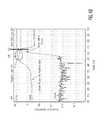
- FIGS. 6A , 6 B, 7 A, and 7 Bare example secondary ion mass spectrometry (SIMS) depth resolution profiles showing the effect upon carbon diffusion into the polysilicon layer by including a barrier layer such as 510 or 520 .
- concentration levelsnormalized to show relative differences in concentration (e.g., not actual concentration), are provided as a function of depth through a stack of materials labeled in the “A” diagram for each figure.
- FIG. 6Aprovides a SIMS depth resolution profiles 610 .
- SIMS depth resolution profile 610illustrates silicon, carbon and oxygen normalized concentration levels through an interface 612 between a polysilicon layer 614 and a TEOS-based SiO 2 layer 616 .
- SIMS depth resolution profile 610shows concentration levels at varying depths through the interface subsequent to deposition of the TEOS-based SiO 2 layer but prior to heating that would be associated with an anneal.
- the carbon profileshows an increase in carbon levels at the interface region into the polysilicon layer to about 10 nm.
- FIG. 6Bprovides a SIMS depth resolution profile 620 .
- SIMS depth resolution profile 620also shows normalized concentration levels at varying depths through the interface but subsequent to heating the structure to temperatures associated with an anneal.
- the carbon profileshows increased carbon levels throughout polysilicon layer 624 , with especially elevated carbon levels to a depth of about 50 nm from interface 622 (e.g., region 628 )
- FIG. 7A and 7Bprovides two SIMS depth resolution profiles in which a poly-SiGeC barrier layer is formed between the polysilicon layer and the TEOS-SiO 2 layer.
- the depth of the barrier poly-SiGeC layeris approximately 450 ⁇ .
- SIMS depth resolution profile 710illustrates the concentration profiles prior to heating to anneal temperatures
- SIMS depth resolution profile 720illustrates the concentration profiles subsequent to heating to anneal temperatures.
- carbon levelsremain low within polysilicon layers 712 and 722 , while the carbon levels in the TEOS-based SiO 2 layers remain higher.
- barrier layer thicknessis kept below about 1000 ⁇ for either barrier 510 or 520 .
- too thick a barrier layer 510may affect subsequent photolithography processes.
- a carbon-diffusion barrier layersuch as poly-SiGeC
- carbon from an external sourcesuch as a TEOS-based SiO 2 layer is prevented from diffusing into an adjacent polysilicon region.
- the majority of the external carbon from the TEOS-based SiO 2 layerremains in the SiO 2 layer and can then be removed as part of the typical process flow for formation of MEMS devices. This will reduce the number of carbon-related stiction failures of MEMS devices (e.g., accelerometers) in the field and will also improve device yield during manufacture.
- one advantage of reducing stiction in accelerometer-type MEMS devicesis improved sensitivity of the device.
- stiction forceis countered by increasing a spring constant of the device. But increasing the spring constant decreases sensitivity of the MEMS device to light acceleration forces.
- chances for stiction occurringare sought to be reduced by increasing the distance between the movable portions of the device and the fixed portions of the device. But this increases the distance between the capacitive plates and can therefore decrease differences in measured capacitance.
- Reducing stiction forces by using embodiments of the present inventionallow for lower spring constants and smaller distances between parts, both of which can improve device sensitivity.
- smaller overall device sizescan be realized by decreasing the distances between the parts. This can, in turn, provide a decreased footprint for each MEMS device, thereby allowing for incorporation of more MEMS devices in a system or a smaller system size.
- a method for manufacturing a micro-electromechanical systems devicethat includes: forming a first polysilicon layer over a substrate; forming a sacrificial layer over the first polysilicon layer where the sacrificial layer includes silicon oxide deposited using TEOS gas; forming a second polysilicon layer over the sacrificial layer; annealing the second polysilicon layer where the annealing includes heating the first and second polysilicon layers and the sacrificial layer to a temperature sufficient to relieve stress in the second polysilicon layer; and forming a carbon barrier layer between the sacrificial layer and one or more of the first and second polysilicon layers.
- the carbon barrier layerprevents diffusion of carbon into an adjacent polysilicon layer from the sacrificial layer during the annealing.
- the carbon barrier layerincludes one of silicon nitride or silicon-germanium-carbon. In another aspect of the above embodiment, forming the carbon barrier layer includes depositing the carbon barrier layer to a thickness of about 45 nm or greater.
- forming the carbon barrier layerincludes forming the carbon barrier layer over and in contact with at least a portion of the first polysilicon layer and forming the carbon barrier layer prior to forming the sacrificial layer. In another aspect of the above embodiment, forming the carbon barrier layer includes forming the carbon barrier layer over and in contact with the sacrificial layer, where forming the carbon barrier layer is performed prior to forming the second polysilicon layer and at least a portion of the second polysilicon layer is formed in contact with the carbon barrier layer.
- Another aspect of the above embodimentincludes removing the sacrificial layer after annealing, using a wet etch. In a further aspect, the method includes removing the carbon barrier layer after annealing. Another aspect of the above embodiment further includes forming a first insulating layer over the substrate where the first polysilicon layer is formed over the first insulating layer, and forming a second insulating layer over at least a portion of the first polysilicon layer.
- Another embodiment of the present inventionprovides a micro-electromechanical systems device that includes: a fixed surface having a first polysilicon layer formed over a substrate and a first insulating layer formed over at least a portion of the first polysilicon layer; a movable body including a second polysilicon layer providing a major surface facing the fixed surface; and a carbon barrier layer formed on at least one of the first polysilicon layer and the major surface of the second polysilicon layer.
- the carbon barrier layerincludes one of silicon nitride or silicon-germanium-carbon.
- the carbon barrier layerincludes a thickness sufficient to prevent diffusion of carbon into the adjacent polysilicon layer from a TEOS sacrificial layer used during manufacture of the MEMS device. In a further aspect, the thickness of the carbon barrier layer is at least about 45 nm. In another aspect of the above embodiment, the MEMS device is an accelerometer.
- Another embodiment of the present inventionprovides a method of manufacturing a micro-electromechanical systems device, wherein the method includes: forming a fixed surface comprising a first layer of polysilicon; forming a movable body providing a major surface facing the fixed surface where at least a portion of the major surface is configured to contact at least a portion of the fixed surface at the at least a portion of the major surface includes a second layer of polysilicon; forming a sacrificial layer between the fixed surface of the movable body where the second sacrificial layer includes silicon oxide deposited using TEOS gas; and forming at least one of the first layer of polysilicon or the second layer of polysilicon such that carbon from the sacrificial layer does not diffuse into the at least one of the first layer or second layer of polysilicon.
- forming the at least one of the first layer of polysilicon or the second layer of polysilicon such that carbon from the sacrificial layer does not diffuse into the at least one of the first layer or second layer of polysiliconfurther includes forming a carbon barrier layer between the sacrificial layer and the at least one of the first layer or second layer of polysilicon.
- the carbon barrier layerprevent diffusion of carbon into the adjacent polysilicon layer from the sacrificial layer during an anneal of the second layer of polysilicon.
- the carbon barrier layerincludes one of silicon nitride or silicon-germanium-carbon.
- forming the carbon barrier layerincludes depositing the carbon barrier layer to a thickness of at least about 45 nm.
- any two components herein combined to achieve a particular functionalitycan be seen as “associated with” each other such that the desired functionality is achieved, irrespective of architectures or intermedial components.
- any two components so associatedcan also be viewed as being “operably connected,” or “operably coupled,” to each other to achieve the desired functionality.
- Embodiments of the present inventionare not limited to teeter-totter accelerometers, but can include accelerometers having a mass suspended by springs, or other MEMS devices that have a potential for components to come in contact with one another during operation or manufacture. Accordingly, the specification and figures are to be regarded in an illustrative rather than a restrictive sense, and all such modifications are intended to be included within the scope of the present invention. Any benefits, advantages, or solutions to problems that are described herein with regard to specific embodiments are not intended to be construed as a critical, required, or essential feature or element of any or all the claims.
- Coupledis not intended to be limited to a direct coupling or a mechanical coupling.
Landscapes
- Engineering & Computer Science (AREA)
- Manufacturing & Machinery (AREA)
- Microelectronics & Electronic Packaging (AREA)
- Physics & Mathematics (AREA)
- General Physics & Mathematics (AREA)
- Computer Hardware Design (AREA)
- Micromachines (AREA)
- Pressure Sensors (AREA)
Abstract
Description

Claims (12)
Priority Applications (5)
| Application Number | Priority Date | Filing Date | Title |
|---|---|---|---|
| US13/718,598US8895339B2 (en) | 2012-12-18 | 2012-12-18 | Reducing MEMS stiction by introduction of a carbon barrier |
| EP13196313.4AEP2746217B1 (en) | 2012-12-18 | 2013-12-09 | Reducing MEMS stiction by introduction of a carbon barrier layer |
| TW102145770ATW201432819A (en) | 2012-12-18 | 2013-12-12 | Reducing MEMS stiction by introduction of a carbon barrier |
| CN201310692997.7ACN103864006B (en) | 2012-12-18 | 2013-12-17 | Reducing MEMS stiction by introduction of a carbon barrier |
| US14/529,824US9463973B2 (en) | 2012-12-18 | 2014-10-31 | Reducing MEMS stiction by introduction of a carbon barrier |
Applications Claiming Priority (1)
| Application Number | Priority Date | Filing Date | Title |
|---|---|---|---|
| US13/718,598US8895339B2 (en) | 2012-12-18 | 2012-12-18 | Reducing MEMS stiction by introduction of a carbon barrier |
Related Child Applications (2)
| Application Number | Title | Priority Date | Filing Date |
|---|---|---|---|
| EP13196313.4APreviously-Filed-ApplicationEP2746217B1 (en) | 2012-12-18 | 2013-12-09 | Reducing MEMS stiction by introduction of a carbon barrier layer |
| US14/529,824DivisionUS9463973B2 (en) | 2012-12-18 | 2014-10-31 | Reducing MEMS stiction by introduction of a carbon barrier |
Publications (2)
| Publication Number | Publication Date |
|---|---|
| US20140167188A1 US20140167188A1 (en) | 2014-06-19 |
| US8895339B2true US8895339B2 (en) | 2014-11-25 |
Family
ID=50023371
Family Applications (2)
| Application Number | Title | Priority Date | Filing Date |
|---|---|---|---|
| US13/718,598ActiveUS8895339B2 (en) | 2012-12-18 | 2012-12-18 | Reducing MEMS stiction by introduction of a carbon barrier |
| US14/529,824Expired - Fee RelatedUS9463973B2 (en) | 2012-12-18 | 2014-10-31 | Reducing MEMS stiction by introduction of a carbon barrier |
Family Applications After (1)
| Application Number | Title | Priority Date | Filing Date |
|---|---|---|---|
| US14/529,824Expired - Fee RelatedUS9463973B2 (en) | 2012-12-18 | 2014-10-31 | Reducing MEMS stiction by introduction of a carbon barrier |
Country Status (4)
| Country | Link |
|---|---|
| US (2) | US8895339B2 (en) |
| EP (1) | EP2746217B1 (en) |
| CN (1) | CN103864006B (en) |
| TW (1) | TW201432819A (en) |
Cited By (1)
| Publication number | Priority date | Publication date | Assignee | Title |
|---|---|---|---|---|
| US11253963B1 (en) | 2020-08-17 | 2022-02-22 | Raytheon Company | Separable component assembly having reduced seal stiction |
Families Citing this family (4)
| Publication number | Priority date | Publication date | Assignee | Title |
|---|---|---|---|---|
| US9903718B2 (en)* | 2015-05-28 | 2018-02-27 | Invensense, Inc. | MEMS device mechanical amplitude control |
| US10384929B2 (en) | 2016-03-22 | 2019-08-20 | Murata Manufacturing Co., Ltd. | Impact element for a sensor device and a manufacturing method |
| JP7364163B2 (en)* | 2018-12-13 | 2023-10-18 | 日清紡マイクロデバイス株式会社 | MEMS element and its manufacturing method |
| US11040870B2 (en)* | 2019-07-25 | 2021-06-22 | Taiwan Semiconductor Manufacturing Co., Ltd. | Microelectromechanical systems device having a mechanically robust anti-stiction/outgassing structure |
Citations (9)
| Publication number | Priority date | Publication date | Assignee | Title |
|---|---|---|---|---|
| US5906708A (en) | 1994-11-10 | 1999-05-25 | Lawrence Semiconductor Research Laboratory, Inc. | Silicon-germanium-carbon compositions in selective etch processes |
| US6275324B1 (en)* | 1998-12-14 | 2001-08-14 | Lucent Technologies Inc. | Micromachined tunable optical filter with controllable finesse and passband wavelength position |
| US6404028B1 (en)* | 1997-04-21 | 2002-06-11 | Ford Global Technologies, Inc. | Adhesion resistant micromachined structure and coating |
| US6531331B1 (en)* | 2002-07-16 | 2003-03-11 | Sandia Corporation | Monolithic integration of a MOSFET with a MEMS device |
| US6838304B2 (en)* | 2001-12-26 | 2005-01-04 | Sony Corporation | MEMS element manufacturing method |
| WO2007021396A2 (en) | 2005-08-16 | 2007-02-22 | Robert Bosch Gmbh | Microelectromechanical devices and fabrication methods |
| US7652547B1 (en)* | 2007-03-22 | 2010-01-26 | Sandia Corporation | Microelectromechanical resonator and method for fabrication |
| US20120080690A1 (en)* | 2010-09-30 | 2012-04-05 | Infineon Technologies Austria Ag | Method for Manufacturing a Composite Wafer Having a Graphite Core, and Composite Wafer Having a Graphite Core |
| EP2489629A2 (en) | 2011-02-16 | 2012-08-22 | Freescale Semiconductor, Inc. | Mems device having variable gap width and method of manufacture |
Family Cites Families (5)
| Publication number | Priority date | Publication date | Assignee | Title |
|---|---|---|---|---|
| US6909186B2 (en)* | 2003-05-01 | 2005-06-21 | International Business Machines Corporation | High performance FET devices and methods therefor |
| US7121141B2 (en)* | 2005-01-28 | 2006-10-17 | Freescale Semiconductor, Inc. | Z-axis accelerometer with at least two gap sizes and travel stops disposed outside an active capacitor area |
| US8536628B2 (en)* | 2007-11-29 | 2013-09-17 | Micron Technology, Inc. | Integrated circuit having memory cell array including barriers, and method of manufacturing same |
| CN101844739A (en)* | 2009-03-27 | 2010-09-29 | 深迪半导体(上海)有限公司 | Manufacturing method of subminiature MEMS gyroscope sensor |
| CN101533832A (en)* | 2009-04-14 | 2009-09-16 | 李刚 | Integrated chips of Micro-electro-mechanism system device and integrated circuit, and integration method |
- 2012
- 2012-12-18USUS13/718,598patent/US8895339B2/enactiveActive
- 2013
- 2013-12-09EPEP13196313.4Apatent/EP2746217B1/ennot_activeNot-in-force
- 2013-12-12TWTW102145770Apatent/TW201432819A/enunknown
- 2013-12-17CNCN201310692997.7Apatent/CN103864006B/ennot_activeExpired - Fee Related
- 2014
- 2014-10-31USUS14/529,824patent/US9463973B2/ennot_activeExpired - Fee Related
Patent Citations (10)
| Publication number | Priority date | Publication date | Assignee | Title |
|---|---|---|---|---|
| US5906708A (en) | 1994-11-10 | 1999-05-25 | Lawrence Semiconductor Research Laboratory, Inc. | Silicon-germanium-carbon compositions in selective etch processes |
| US6404028B1 (en)* | 1997-04-21 | 2002-06-11 | Ford Global Technologies, Inc. | Adhesion resistant micromachined structure and coating |
| US6275324B1 (en)* | 1998-12-14 | 2001-08-14 | Lucent Technologies Inc. | Micromachined tunable optical filter with controllable finesse and passband wavelength position |
| US6838304B2 (en)* | 2001-12-26 | 2005-01-04 | Sony Corporation | MEMS element manufacturing method |
| US6531331B1 (en)* | 2002-07-16 | 2003-03-11 | Sandia Corporation | Monolithic integration of a MOSFET with a MEMS device |
| WO2007021396A2 (en) | 2005-08-16 | 2007-02-22 | Robert Bosch Gmbh | Microelectromechanical devices and fabrication methods |
| US7652547B1 (en)* | 2007-03-22 | 2010-01-26 | Sandia Corporation | Microelectromechanical resonator and method for fabrication |
| US20120080690A1 (en)* | 2010-09-30 | 2012-04-05 | Infineon Technologies Austria Ag | Method for Manufacturing a Composite Wafer Having a Graphite Core, and Composite Wafer Having a Graphite Core |
| EP2489629A2 (en) | 2011-02-16 | 2012-08-22 | Freescale Semiconductor, Inc. | Mems device having variable gap width and method of manufacture |
| EP2489629A3 (en) | 2011-02-16 | 2014-07-02 | Freescale Semiconductor, Inc. | Mems device having variable gap width and method of manufacture |
Cited By (1)
| Publication number | Priority date | Publication date | Assignee | Title |
|---|---|---|---|---|
| US11253963B1 (en) | 2020-08-17 | 2022-02-22 | Raytheon Company | Separable component assembly having reduced seal stiction |
Also Published As
| Publication number | Publication date |
|---|---|
| US9463973B2 (en) | 2016-10-11 |
| EP2746217A1 (en) | 2014-06-25 |
| TW201432819A (en) | 2014-08-16 |
| EP2746217B1 (en) | 2016-10-12 |
| CN103864006B (en) | 2017-04-12 |
| CN103864006A (en) | 2014-06-18 |
| US20150054096A1 (en) | 2015-02-26 |
| US20140167188A1 (en) | 2014-06-19 |
Similar Documents
| Publication | Publication Date | Title |
|---|---|---|
| US9776853B2 (en) | Reducing MEMS stiction by deposition of nanoclusters | |
| US9463973B2 (en) | Reducing MEMS stiction by introduction of a carbon barrier | |
| US9213045B2 (en) | Active lateral force stiction self-recovery for microelectromechanical systems devices | |
| US9550664B2 (en) | Reducing MEMS stiction by increasing surface roughness | |
| US8362578B2 (en) | Triple-axis MEMS accelerometer | |
| EP2344416B1 (en) | Plurality of smaller mems devices to replace a larger mems device | |
| US7736931B1 (en) | Wafer process flow for a high performance MEMS accelerometer | |
| US20050255645A1 (en) | Anti-stiction technique for thin film and wafer-bonded encapsulated microelectromechanical systems | |
| US8119431B2 (en) | Method of forming a micro-electromechanical system (MEMS) having a gap stop | |
| CN109890749B (en) | MEMS structure with graphene assembly | |
| KR102320644B1 (en) | Micro-electro mechanical system device containing a bump stopper and methods for forming the same | |
| TW201728525A (en) | Method to improve stiction by roughing surface | |
| US20220306454A1 (en) | Composite spring structure to reinforce mechanical robustness of a mems device | |
| CN110972048A (en) | Microphone, MEMS device and method of manufacturing MEMS device | |
| US9108842B2 (en) | Reducing microelectromechanical systems stiction by formation of a silicon carbide layer | |
| US8088692B2 (en) | Method for fabricating a multilayer microstructure with balancing residual stress capability | |
| US9434602B2 (en) | Reducing MEMS stiction by deposition of nanoclusters | |
| US10427929B1 (en) | Forming a eutectic bond between a wafer having an anti-stiction coating and a cap wafer | |
| US11180363B2 (en) | Outgassing material coated cavity for a micro-electro mechanical system device and methods for forming the same | |
| TWI826585B (en) | Method for manufacturing an integrated mems transducer device and integrated mems transducer device | |
| KR100701151B1 (en) | Method of manufacturing flotation structure for micromechanical integration system | |
| JP2019155544A (en) | Mems element and manufacturing method thereof |
Legal Events
| Date | Code | Title | Description |
|---|---|---|---|
| AS | Assignment | Owner name:FREESCALE SEMICONDUCTOR, INC., TEXAS Free format text:ASSIGNMENT OF ASSIGNORS INTEREST;ASSIGNORS:MONTEZ, RUBEN B.;STEIMLE, ROBERT F.;SIGNING DATES FROM 20121214 TO 20121218;REEL/FRAME:029492/0909 | |
| AS | Assignment | Owner name:CITIBANK, N.A., AS NOTES COLLATERAL AGENT, NEW YORK Free format text:SUPPLEMENT TO IP SECURITY AGREEMENT;ASSIGNOR:FREESCALE SEMICONDUCTOR, INC.;REEL/FRAME:030258/0558 Effective date:20130214 Owner name:CITIBANK, N.A., AS NOTES COLLATERAL AGENT, NEW YORK Free format text:SUPPLEMENT TO IP SECURITY AGREEMENT;ASSIGNOR:FREESCALE SEMICONDUCTOR, INC.;REEL/FRAME:030258/0523 Effective date:20130214 Owner name:CITIBANK, N.A., AS NOTES COLLATERAL AGENT, NEW YOR Free format text:SUPPLEMENT TO IP SECURITY AGREEMENT;ASSIGNOR:FREESCALE SEMICONDUCTOR, INC.;REEL/FRAME:030258/0558 Effective date:20130214 Owner name:CITIBANK, N.A., AS NOTES COLLATERAL AGENT, NEW YOR Free format text:SUPPLEMENT TO IP SECURITY AGREEMENT;ASSIGNOR:FREESCALE SEMICONDUCTOR, INC.;REEL/FRAME:030258/0523 Effective date:20130214 Owner name:CITIBANK, N.A., AS COLLATERAL AGENT, NEW YORK Free format text:SUPPLEMENT TO IP SECURITY AGREEMENT;ASSIGNOR:FREESCALE SEMICONDUCTOR, INC.;REEL/FRAME:030258/0540 Effective date:20130214 | |
| AS | Assignment | Owner name:CITIBANK, N.A., AS NOTES COLLATERAL AGENT, NEW YORK Free format text:SECURITY AGREEMENT;ASSIGNOR:FREESCALE SEMICONDUCTOR, INC.;REEL/FRAME:030633/0424 Effective date:20130521 Owner name:CITIBANK, N.A., AS NOTES COLLATERAL AGENT, NEW YOR Free format text:SECURITY AGREEMENT;ASSIGNOR:FREESCALE SEMICONDUCTOR, INC.;REEL/FRAME:030633/0424 Effective date:20130521 | |
| AS | Assignment | Owner name:CITIBANK, N.A., AS NOTES COLLATERAL AGENT, NEW YORK Free format text:SECURITY AGREEMENT;ASSIGNOR:FREESCALE SEMICONDUCTOR, INC.;REEL/FRAME:031591/0266 Effective date:20131101 Owner name:CITIBANK, N.A., AS NOTES COLLATERAL AGENT, NEW YOR Free format text:SECURITY AGREEMENT;ASSIGNOR:FREESCALE SEMICONDUCTOR, INC.;REEL/FRAME:031591/0266 Effective date:20131101 | |
| STCF | Information on status: patent grant | Free format text:PATENTED CASE | |
| AS | Assignment | Owner name:FREESCALE SEMICONDUCTOR, INC., TEXAS Free format text:PATENT RELEASE;ASSIGNOR:CITIBANK, N.A., AS COLLATERAL AGENT;REEL/FRAME:037357/0671 Effective date:20151207 Owner name:FREESCALE SEMICONDUCTOR, INC., TEXAS Free format text:PATENT RELEASE;ASSIGNOR:CITIBANK, N.A., AS COLLATERAL AGENT;REEL/FRAME:037357/0685 Effective date:20151207 | |
| AS | Assignment | Owner name:MORGAN STANLEY SENIOR FUNDING, INC., MARYLAND Free format text:ASSIGNMENT AND ASSUMPTION OF SECURITY INTEREST IN PATENTS;ASSIGNOR:CITIBANK, N.A.;REEL/FRAME:037486/0517 Effective date:20151207 | |
| AS | Assignment | Owner name:MORGAN STANLEY SENIOR FUNDING, INC., MARYLAND Free format text:ASSIGNMENT AND ASSUMPTION OF SECURITY INTEREST IN PATENTS;ASSIGNOR:CITIBANK, N.A.;REEL/FRAME:037518/0292 Effective date:20151207 | |
| AS | Assignment | Owner name:FREESCALE SEMICONDUCTOR, INC., TEXAS Free format text:PATENT RELEASE;ASSIGNOR:CITIBANK, N.A., AS COLLATERAL AGENT;REEL/FRAME:037494/0312 Effective date:20151207 | |
| AS | Assignment | Owner name:MORGAN STANLEY SENIOR FUNDING, INC., MARYLAND Free format text:SUPPLEMENT TO THE SECURITY AGREEMENT;ASSIGNOR:FREESCALE SEMICONDUCTOR, INC.;REEL/FRAME:039138/0001 Effective date:20160525 | |
| AS | Assignment | Owner name:NXP, B.V., F/K/A FREESCALE SEMICONDUCTOR, INC., NETHERLANDS Free format text:RELEASE BY SECURED PARTY;ASSIGNOR:MORGAN STANLEY SENIOR FUNDING, INC.;REEL/FRAME:040925/0001 Effective date:20160912 Owner name:NXP, B.V., F/K/A FREESCALE SEMICONDUCTOR, INC., NE Free format text:RELEASE BY SECURED PARTY;ASSIGNOR:MORGAN STANLEY SENIOR FUNDING, INC.;REEL/FRAME:040925/0001 Effective date:20160912 | |
| AS | Assignment | Owner name:NXP B.V., NETHERLANDS Free format text:RELEASE BY SECURED PARTY;ASSIGNOR:MORGAN STANLEY SENIOR FUNDING, INC.;REEL/FRAME:040928/0001 Effective date:20160622 | |
| AS | Assignment | Owner name:NXP USA, INC., TEXAS Free format text:MERGER;ASSIGNOR:FREESCALE SEMICONDUCTOR, INC.;REEL/FRAME:041144/0363 Effective date:20161107 | |
| AS | Assignment | Owner name:MORGAN STANLEY SENIOR FUNDING, INC., MARYLAND Free format text:CORRECTIVE ASSIGNMENT TO CORRECT THE REMOVE PATENTS 8108266 AND 8062324 AND REPLACE THEM WITH 6108266 AND 8060324 PREVIOUSLY RECORDED ON REEL 037518 FRAME 0292. ASSIGNOR(S) HEREBY CONFIRMS THE ASSIGNMENT AND ASSUMPTION OF SECURITY INTEREST IN PATENTS;ASSIGNOR:CITIBANK, N.A.;REEL/FRAME:041703/0536 Effective date:20151207 | |
| MAFP | Maintenance fee payment | Free format text:PAYMENT OF MAINTENANCE FEE, 4TH YEAR, LARGE ENTITY (ORIGINAL EVENT CODE: M1551) Year of fee payment:4 | |
| AS | Assignment | Owner name:SHENZHEN XINGUODU TECHNOLOGY CO., LTD., CHINA Free format text:CORRECTIVE ASSIGNMENT TO CORRECT THE TO CORRECT THE APPLICATION NO. FROM 13,883,290 TO 13,833,290 PREVIOUSLY RECORDED ON REEL 041703 FRAME 0536. ASSIGNOR(S) HEREBY CONFIRMS THE THE ASSIGNMENT AND ASSUMPTION OF SECURITYINTEREST IN PATENTS.;ASSIGNOR:MORGAN STANLEY SENIOR FUNDING, INC.;REEL/FRAME:048734/0001 Effective date:20190217 | |
| AS | Assignment | Owner name:NXP B.V., NETHERLANDS Free format text:RELEASE BY SECURED PARTY;ASSIGNOR:MORGAN STANLEY SENIOR FUNDING, INC.;REEL/FRAME:050744/0097 Effective date:20190903 | |
| AS | Assignment | Owner name:MORGAN STANLEY SENIOR FUNDING, INC., MARYLAND Free format text:CORRECTIVE ASSIGNMENT TO CORRECT THE REMOVE APPLICATION11759915 AND REPLACE IT WITH APPLICATION 11759935 PREVIOUSLY RECORDED ON REEL 037486 FRAME 0517. ASSIGNOR(S) HEREBY CONFIRMS THE ASSIGNMENT AND ASSUMPTION OF SECURITYINTEREST IN PATENTS;ASSIGNOR:CITIBANK, N.A.;REEL/FRAME:053547/0421 Effective date:20151207 | |
| AS | Assignment | Owner name:NXP B.V., NETHERLANDS Free format text:CORRECTIVE ASSIGNMENT TO CORRECT THE REMOVEAPPLICATION 11759915 AND REPLACE IT WITH APPLICATION11759935 PREVIOUSLY RECORDED ON REEL 040928 FRAME 0001. ASSIGNOR(S) HEREBY CONFIRMS THE RELEASE OF SECURITYINTEREST;ASSIGNOR:MORGAN STANLEY SENIOR FUNDING, INC.;REEL/FRAME:052915/0001 Effective date:20160622 | |
| AS | Assignment | Owner name:NXP, B.V. F/K/A FREESCALE SEMICONDUCTOR, INC., NETHERLANDS Free format text:CORRECTIVE ASSIGNMENT TO CORRECT THE REMOVEAPPLICATION 11759915 AND REPLACE IT WITH APPLICATION11759935 PREVIOUSLY RECORDED ON REEL 040925 FRAME 0001. ASSIGNOR(S) HEREBY CONFIRMS THE RELEASE OF SECURITYINTEREST;ASSIGNOR:MORGAN STANLEY SENIOR FUNDING, INC.;REEL/FRAME:052917/0001 Effective date:20160912 | |
| MAFP | Maintenance fee payment | Free format text:PAYMENT OF MAINTENANCE FEE, 8TH YEAR, LARGE ENTITY (ORIGINAL EVENT CODE: M1552); ENTITY STATUS OF PATENT OWNER: LARGE ENTITY Year of fee payment:8 |