US8891595B1 - Electromagnetic interference reduction in wireline applications using differential signal compensation - Google Patents
Electromagnetic interference reduction in wireline applications using differential signal compensationDownload PDFInfo
- Publication number
- US8891595B1 US8891595B1US13/790,333US201313790333AUS8891595B1US 8891595 B1US8891595 B1US 8891595B1US 201313790333 AUS201313790333 AUS 201313790333AUS 8891595 B1US8891595 B1US 8891595B1
- Authority
- US
- United States
- Prior art keywords
- signal
- common mode
- differential
- circuit
- differential signal
- Prior art date
- Legal status (The legal status is an assumption and is not a legal conclusion. Google has not performed a legal analysis and makes no representation as to the accuracy of the status listed.)
- Active, expires
Links
Images


Classifications
- H—ELECTRICITY
- H04—ELECTRIC COMMUNICATION TECHNIQUE
- H04L—TRANSMISSION OF DIGITAL INFORMATION, e.g. TELEGRAPHIC COMMUNICATION
- H04L12/00—Data switching networks
- H04L12/02—Details
- H04L12/10—Current supply arrangements
- H—ELECTRICITY
- H04—ELECTRIC COMMUNICATION TECHNIQUE
- H04B—TRANSMISSION
- H04B1/00—Details of transmission systems, not covered by a single one of groups H04B3/00 - H04B13/00; Details of transmission systems not characterised by the medium used for transmission
- H04B1/02—Transmitters
- H04B1/04—Circuits
- H04B1/0475—Circuits with means for limiting noise, interference or distortion
- H—ELECTRICITY
- H04—ELECTRIC COMMUNICATION TECHNIQUE
- H04L—TRANSMISSION OF DIGITAL INFORMATION, e.g. TELEGRAPHIC COMMUNICATION
- H04L12/00—Data switching networks
- H04L12/28—Data switching networks characterised by path configuration, e.g. LAN [Local Area Networks] or WAN [Wide Area Networks]
- H04L12/40—Bus networks
- H04L12/407—Bus networks with decentralised control
- H04L12/413—Bus networks with decentralised control with random access, e.g. carrier-sense multiple-access with collision detection [CSMA-CD]
- H—ELECTRICITY
- H04—ELECTRIC COMMUNICATION TECHNIQUE
- H04L—TRANSMISSION OF DIGITAL INFORMATION, e.g. TELEGRAPHIC COMMUNICATION
- H04L25/00—Baseband systems
- H04L25/02—Details ; arrangements for supplying electrical power along data transmission lines
- H04L25/0264—Arrangements for coupling to transmission lines
- H04L25/0266—Arrangements for providing Galvanic isolation, e.g. by means of magnetic or capacitive coupling
- H—ELECTRICITY
- H04—ELECTRIC COMMUNICATION TECHNIQUE
- H04L—TRANSMISSION OF DIGITAL INFORMATION, e.g. TELEGRAPHIC COMMUNICATION
- H04L25/00—Baseband systems
- H04L25/02—Details ; arrangements for supplying electrical power along data transmission lines
- H04L25/0264—Arrangements for coupling to transmission lines
- H04L25/0272—Arrangements for coupling to multiple lines, e.g. for differential transmission
- H—ELECTRICITY
- H04—ELECTRIC COMMUNICATION TECHNIQUE
- H04L—TRANSMISSION OF DIGITAL INFORMATION, e.g. TELEGRAPHIC COMMUNICATION
- H04L25/00—Baseband systems
- H04L25/02—Details ; arrangements for supplying electrical power along data transmission lines
- H04L25/0264—Arrangements for coupling to transmission lines
- H04L25/028—Arrangements specific to the transmitter end
Definitions
- the disclosure hereinrelates to electronic communications, and more particularly to mitigating imbalance in transceiver circuitry and interference in signals transmitted over communication channels.
- Transceivers of a communication systemsend and receive data over a link (including one or more channels) of a communication network to communicate with other transceivers.
- a transceiverincludes a transmitter for sending information across a link, and a receiver for receiving information from the link. The receiver detects transmitted data from a link partner transceiver on the opposite end of the link and converts the data into a form usable by the system connected to the transceiver.
- one widely-used network communication standardis Ethernet, including several different standards for different network bandwidths, including 10 GBASE-T allowing 10 gigabit/second connections over unshielded or shielded twisted pair cables.
- ISIinter-symbol interference
- FEXTfar-end crosstalk
- NXTnear-end crosstalk
- Other examples of internal interferenceinclude differential skew between the two differential signal components in the channel (e.g., imbalance in the channels) and driver circuit asymmetry generating different transition for rising and falling edges (e.g., imbalance of the differential drivers).
- Typical causes of imbalance in the channelsinclude, for example, unequal stray coupling of the traces (or wireline), differences between two trace widths, propagation time differences caused by woven printed circuit board (PCB) substrate, change in PCB layer and coating on micro-strips, transformer unequal windings for the two differential signal components, and crimping of the wires in the plug and in connection to connectors.
- Typical causes of imbalance of the differential driversinclude, for example, termination impedance mismatch, and differential switching circuitry not having the same response for the respective falling and rising edges.
- differential signal imbalancemay lead to levels of common-mode that cause undesirable RF emissions during signal transmissions along the channel.
- Transceiver designsoften must meet stringent Federal Communications Commission (FCC) rules and regulations regarding spurious emissions in order to avoid interfering with other communications equipment.
- FCCFederal Communications Commission
- FIG. 1illustrates a block diagram of one embodiment of a high-level 10 GBASE-T transceiver architecture
- FIG. 2Aillustrates an ideal case of a balanced differential signal with a flat common mode signal
- FIG. 2Billustrates an example of a differential signal experiencing one type of noise interference and its associated common mode signal
- FIG. 2Cillustrates an example of an adjusted differential signal with a signal characteristic opposite to the interfered signal of FIG. 2B ;
- FIG. 2Dillustrates an example of a differential signal experiencing another type of noise interference and its associated common mode signal
- FIG. 2Eillustrates an example of an adjusted differential signal with a signal characteristic opposite to the interfered signal of FIG. 2D ;
- FIG. 3illustrates an embodiment of a common mode signal detector to provide a common mode signal in a communication system to allow interference caused by a noise source to be determined;
- FIG. 4illustrates one embodiment of a transceiver employing a compensator circuit for interference compensation
- FIGS. 5A , 5 B, 5 C, and 5 Dillustrate various detailed embodiments of the compensator circuit of FIG. 4 ;
- FIG. 6illustrates a further embodiment of a compensator circuit similar to the embodiments shown in FIGS. 5A-5D ;
- FIG. 7illustrates an embodiment of a multi-channel transceiver device employing at least one common mode signal detection circuit for interference compensation
- FIG. 8is a flow diagram illustrating a method of providing interference compensation based on a detected common mode signal
- FIG. 9illustrates one embodiment of a transmit circuit that employs on-chip compensation circuitry to address imbalance in differential signal components
- FIG. 10Aillustrates a timing diagram showing how an accumulating integrator waveform is generated when a detected common-mode is positive
- FIG. 10Billustrates a timing diagram showing how an accumulating integrator waveform is generated when a detected common-mode is negative.
- FIG. 11illustrates an embodiment of a transmit circuit similar to the transmit circuit of FIG. 9 , and including a replica branch path.
- Embodiments of an integrated circuit deviceare disclosed.
- One embodiment of the integrated circuit deviceincludes a differential driver to generate a differential signal having true and complement signal components that exhibit a relative timing relationship.
- a transmission port coupled to the output of the differential driverprovides an interface for delivering the differential signal to a transmission medium.
- a common mode detection circuitdetects a common mode signal associated with the differential signal.
- Control circuitrygenerates a control signal based on the detected common mode signal.
- Timing circuitryadjusts the relative timing between the true and the complement signal components based on the control signal.
- a method of reducing radio frequency interference (RFI) emitted by a differential driverincludes generating a differential signal having a true signal component and a complement signal component for transmission along a transmission medium. A level of common mode associated with the generated differential signal is detected prior to transmission on the medium and a signal generated indicative of the detected level. The detected common mode signal is accumulated with previously detected common mode signals to generate a running accumulation value. The running accumulation value is compared to a predetermined threshold and a relative timing adjusted between the true signal component and the complement signal component if the predetermined threshold is exceeded.
- RFIDradio frequency interference
- FIG. 1is a block diagram illustrating one embodiment of a 10 GBASE-T communication system 100 suitable for use with embodiments described herein.
- the system 100includes a first transceiver integrated circuit (IC) or chip 102 and a second transceiver chip 104 that can communicate with each other.
- the first transceiver 102includes “transceiver components” including one or more transmitters TX A -TX A and one or more receivers RX A -RX D .
- the second transceiver 104includes various transceiver components including one or more transmitters TX E -TX H and one or more receivers RX E -RX H .
- receivers RX A -RX Hcan be considered individual “receivers,” as typically referenced herein, or can alternately be considered individual receiver channels on which a receiver block within the transceiver can independently receive signals.
- the transmitters and receiversare connected to one or more components (not shown) of a computer system, device, processor, or other “controller” associated with each respective transceiver which wants to communicate data over the communication network.
- the transmittersreceive data and control signals from the controller connected to the first transceiver 102 in order to send the data over the network to other transceivers and controllers, while the receivers receive data from other transceivers and controllers via the network in order to provide the data to the controller connected to the first transceiver 102 .
- the first transceiver chip 102can communicate with the second transceiver chip 104 over one or more communication channels of a communication link 106 .
- a communication link 106In one embodiment, such as that corresponding to the 10 GBASE-T Ethernet standard, four communication channels are provided on the communication link 106 , each channel including a twisted pair cable.
- there are four transmitters TX and four corresponding receivers RX provided in each of the transceivers 102 and 104each transmitter associated with one of the local near-end receivers in the same transceiver, and each such transmitter/receiver pair dedicated to one channel used for duplex communication.
- a transmitter/receiver pair in the first transceiver 102communicates across a channel of the link 106 to a far-end transmitter/receiver pair in the second transceiver 104 .
- a transmitter TX and a receiver RX that are connected to the same channel/link, or two transceivers connected by the communication link 106are considered “link partners.”
- An interface 108can be provided in the first transceiver chip 102 and an interface 110 can be provided in the second transceiver chip 104 to allow data transmissions between the transceivers to be routed to the appropriate transceiver blocks.
- the interfaces 108 and 110can include transformers, and circuitry used for directing signals or data (alternatively, some or all circuitry can be included in other components, such as transmitters TX and receivers RX).
- the interface 108receives data on a corresponding channel of the communication link 106 .
- the datais received by the link partner, the second transceiver chip 104 .
- the interface 110 of the transceiver 104provides the received data to its receiver RX connected to that same channel.
- the data transmitted by the transmittersis also received by the near-end receivers in the same transceiver. Filters can be used to filter out this noise so that the receivers receive only data from other transceivers.
- the transceivers 102 and 104are asymmetric, such that data transmitted by a local transmitter has no dependence or relation with data being received by the corresponding local receiver.
- interferencecan be categorized by noise source into two categories, external (or alien) and internal. Interference can also be categorized by the signal characteristic it affects, for example, timing and amplitude. Of course, interference that affects the same type of signal characteristic can result from different noise sources, and interference that affects different types of signal characteristics can result from the same noise source.
- a typical result from internal interferenceis an imbalance in the transceiver circuitry.
- a typical result of alien interferenceis an imbalance in the channels.
- Other sourcesmay include RFI or cross-talk, as discussed above.
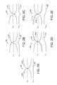
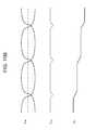
- FIG. 2Aillustrates an ideal balanced differential signal 200 with a flat common mode signal 220 .
- a common mode signal 220is the summation of two differential signal components 210 a and 210 b , which collectively represent a differential signal 220 .
- the two differential signal components 210 a and 210 bare perfectly complementary to each other so that their corresponding common mode signal 220 remains flat, with a zero offset. If, for example, a circuit imbalance affects both of the two differential signal components 210 a and 210 b equally, then the corresponding common mode signal 220 still remains flat, and the effect of the imbalance can be readily suppressed via well-known methods.
- the common mode signal 220is a non-flat curve, then it indicates an imbalance having different levels of impact on each of the two differential signal components 210 a and 210 b . Any non-flat common mode signal is undesirable as such an imbalance often requires further processing to reduce its effect.
- FIG. 2Billustrates an example of a differential signal 202 experiencing a timing type of imbalance and its associated common mode signal 222 .
- one or both of the two differential signal components (e.g., differential signal component 212 ) of the differential signal 202is shifted in time with respect to one another (e.g., from an internal imbalance in the channel) so that the two components are no longer completely complementary.
- the common mode signal 222 corresponding to differential signal 202therefore, manifests a protrusion near the center point where the two differential components cross over each other.
- FIG. 2Cillustrates an example of an adjusted differential signal 204 with a signal characteristic opposite to the interfered differential signal 202 of FIG. 2B .
- adjusted differential signal 204is shown to be deliberately adjusted, by circuitry more fully described below, to have a signal characteristic that is directly complementary to the differential signal 202 of FIG. 2B in order to compensate the imbalance.
- the common mode signal 224 corresponding to adjusted differential signal 204therefore, shows a depression near the center point where the two differential components cross over each other, and is complementary to the common mode signal 222 of FIG. 2B .
- Adjusted differential signal 204can be generated based upon the common mode signal 224 of FIG. 2C , which is a complementary signal of the common mode signal 222 detected in FIG. 2B .
- FIG. 2Dillustrates an example of a differential signal 206 experiencing an amplitude type of imbalance and its associated common mode signal 226 .
- one of the two differential signal components (e.g., differential signal component 216 ) of the differential signal 206is skewed with different amplification (e.g., from an imbalance of the differential drivers) so that the two components are not completely complementary to each other anymore.
- the common mode signal 226 corresponding to differential signal 206therefore, manifests a curve with a positive slope near the center point where the two differential components cross over each other.
- FIG. 2Eillustrates an example of an adjusted differential signal 208 with a signal characteristic opposite to the interfered differential signal 206 of FIG. 2D .
- adjusted differential signal 208is shown to be deliberately adjusted, with circuitry described more fully below, to have a signal characteristic that is directly complementary to the differential signal 206 of FIG. 2D in order to compensate the imbalance.
- the common mode signal 228 corresponding to adjusted differential signal 208therefore, shows a curve with a negative slope near the center point where the two differential components cross over each other, and is complementary to the common mode signal 226 of FIG. 2D .
- Adjusted differential signal 208can be generated based upon the common mode signal 228 of FIG. 2C , which is a complementary signal of the common mode signal 226 detected in FIG. 2D .
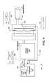
- FIG. 3illustrates an embodiment of a common mode signal detector 320 to provide a common mode signal in a communication system to allow a differential signal imbalance to be determined and compensated.
- the common mode signalmay be directly measured from a transmission channel.
- the common mode signal 330may be measured from a near-end transmission port.
- the common-mode signal detectordetects the common mode signal from a link transformer.
- a coupling transformer 322is provided at the connection point of a transceiver for each communication channel in the link.
- an isolation transformeris provided at both a transmitter end of each channel and at a receiver end of each channel (here, the receiver end is shown), to provide, for example, DC isolation, common mode rejection, impedance matching between dedicated drivers of the transmitter and the impedance of the cable, and balanced data transfer over the cable of the channel.
- FIG. 3is typically known as a “center-tap transformer,” although any other suitable methods or apparatus to detect a common mode signal can be used consistent with the principles described herein.
- one way to pick up the common mode signal from channel Nis from an interference tap, which in one embodiment is a center tap 328 of the coupling transformer 322 .
- the common mode signalis provided on terminals 330 , one terminal connected to the center tap 328 and the other terminal connected to ground.
- This common mode signalcan act as a reference signal, such as the common mode signal 222 of FIG. 2B or the common mode signal 226 of FIG. 2D .
- the detected common mode signal on terminals 330can be provided to suitable compensator circuits or filters (described in more details below) to suppress imbalance experienced by communication channels in the communication system 100 of FIG. 1 .
- an additional receiver pathmay be provided to sense the common mode signal on a receive data channel, where the additional receiver path is referred to herein as a “common mode path.”
- the common mode pathis in addition to any existing receiver paths used for data communication. For example, in a typical 10 GBASE-T system, four receiver paths are used for data communication, one connected to each channel.
- Channel Nis used for tapping the common mode noise signal as shown in FIG. 3 , and can be any one of the existing communication channels.
- the common mode pathis a fifth receiver path used to receive and process the common mode signal in determining imbalance.
- the communication channel Nis connected to the transformer in the usual way.
- the communication linkis connected to the channel N differential terminals 324 , which are connected to an input at one side of the transformer.
- the channel N differential terminals 326are connected to a corresponding output at the other side of the transformer 322 .
- the differential channel N terminals 326are also connected to the standard receiver components to which the usual differential channels are connected.
- FIG. 4illustrates one embodiment of a transceiver circuit 400 employing a compensator circuit 430 for imbalance compensation.
- transceiver 400includes interface circuitry 410 , a common mode signal detection circuit 420 , a compensator circuit 430 , and transmission port 440 .
- the common mode signal detection circuit 420is placed on the transmitter end. This configuration is generally suitable for detection and compensation of imbalance in the interface circuitry 410 .
- common mode signal detection circuit 420can be placed on the receiver end (not shown) for detection and compensation of differential imbalance in the communication channels.
- the interface circuitry 410generally represents the circuit path that a differential signal, after being generated by a differential driver 434 , travels through before arriving transmission port 440 .
- the interface circuitry 410may include any wiring that the differential signal traverses before reaching the communication channel including, for example, wiring inside the transceiver IC packaging, filters, or even the printed circuit board on which the transceiver IC is mounted.
- the common mode signal detection circuit 420is structured the same and functions substantially in the same manner as the common mode signal detector 320 of FIG. 3 .
- Common mode signal detection circuit 420detects imbalance in a differential signal transmitted from interface circuitry 410 and generates a common mode signal on a center tap 428 . From center tap 428 , common mode signal detection circuit 420 feeds the common mode signal to compensator circuit 430 through a common mode path 424 .
- the advantage of sensing the common-mode signal at the line side of the common-mode detector 420is that the compensator can also compensate for any imbalances in the signal path from the transmitter through the interface all the way to the connection point of the channel.
- Common mode signal detection circuit 420also comprises another terminal for the differential signal to pass through to transmission port 440 , which in turn is connected to the communication channels.
- the compensator circuit 430includes an input to receive the common mode signal V com from the common mode path 424 , control circuitry 432 , and the differential driver 434 that responds to the control circuitry in at least one of several possible ways, as more fully described below.
- the control circuitry 432evaluates the detected common-mode signal V com and generates one or more control signals to carry out one more corresponding adjustments to the differential driver circuitry in order to compensate for the differential signal imbalance resulting from the imperfect common mode.
- the compensator circuit 430includes input adjustment circuitry (e.g., embodiments shown in FIGS.
- compensator circuit 430includes adjustable impedance circuitry (e.g., embodiments shown in FIGS. 5C and 5D , described in detail below) to pre-adjust an impedance characteristic of a corresponding part of differential driver circuitry, on which at least one component of the differential signal is transmitted, based on the common mode signal determined by common mode signal detection circuit 420 .
- compensator circuit 430includes a filter (e.g., the embodiment shown in FIG.
- the filtercoupled to the differential driver 434 , the filter generating a compensation signal based on the received common mode signal.
- the compensation signalis to be applied onto the original differential signal to reduce or eliminate differential signal imbalance.
- an embodimentmay have more than one adjustment or filter circuitry to compensate different types of interference.
- compensator circuit 430can dynamically adjust the differential signal output of the differential driver 434 in order to cancel out differential signal imbalance detected by common mode signal detection circuit 420 .
- Different embodiments of adjustment or filter circuitryare discussed with reference to FIG. 5 and FIG. 6 below.
- FIGS. 5A , 5 B, 5 C, and 5 Dillustrate specific embodiments of the compensator circuit of FIG. 4 .
- compensator circuit 510includes a first bias current source or bias impedance 513 a second bias current source 514 , a first signal input 515 coupled to a first switching device Q 1 , and a second signal input 516 coupled to a second switching device Q 2 matched to the first device Q 1 to form what resembles a differential pair.
- the tail connections for the two matched devices Q 1 and Q 2are not coupled together, and thus form a pseudo-differential pair.
- the first and second signal inputs 515 and 516each receive respective differential signal components, such as Vin and Vin .
- a delay circuit Delay 1may be employed in one of the input paths, such as that shown at 515 .
- a second delay circuit Delay 2may be employed in the other input path if desired. Since the matched devices are “decoupled”, introducing an extra timing delay to one differential signal component on one input, (e.g., signal input 515 ) does not affect the response of the other transistor Q 2 . In this way, when a common mode signal indicates that the transceiver is experiencing a timing interference or imbalance, the control circuit (e.g., control circuitry 432 of FIG. 4 ) can adjust the timing (e.g., by adjusting the delay circuit Delay 1 through a control signal Ctrl 1 ) of at least one of the differential signal components that compose the differential signal to compensate the interference.
- the control circuite.g., control circuitry 432 of FIG. 4
- compensator circuit 520includes a bias current source 523 , a first signal input 525 coupled to a first MOS transistor Q 1 , and a second signal input 526 coupled to a second MOS transistor Q 2 matched to the first transistor Q 1 to form a differential pair.
- the first and second signal inputs 525 and 526each receive respective differential signal components, such as Vin and Vin .
- a level adjustment circuit Lvl_Adj 1may be employed in one of the input paths, such as that shown at 525 .
- a second level adjustment circuit Lvl_Adj 2may be employed in the other input path if desired.
- control circuite.g., control circuitry 432 of FIG. 4
- the control circuitcan adjust the signal level (e.g., by adjusting the level adjustment circuit Lvl_Adj 1 through a control signal Ctrl 1 ) of at least one of the differential signal components that compose the differential signal to compensate the interference.
- compensator circuit 530includes a bias current source 533 , a first signal input 535 coupled to a first MOS transistor Q 1 , a second signal input 536 coupled to a second MOS transistor Q 2 matched to the first transistor Q 1 to form a differential pair, a first adjustable resistor 537 to adjust the load resistance on the first transistor Q 1 , and a second adjustable resistor 538 to adjust the load resistance on the second transistor Q 2 .
- the first and second signal inputs 535 and 536each receive respective differential signal components, such as Vin and Vin .
- an adjustable resistor circuit 537may be coupled to the first transistor Q 1 to adjust the DC amplitude thereof.
- a second adjustable resistor circuit 538may be coupled to the second transistor Q 2 to adjust the DC amplitude thereof if desired.
- the control circuite.g., control circuitry 432 of FIG. 4
- the control circuitcan adjust the DC amplitude (e.g., by adjusting the adjustable resistor 537 through a control signal Ctrl 1 ) of at least one of the differential signal components that compose the differential signal to compensate the interference.
- compensator circuit 540includes a bias current source 543 , a first signal input 545 coupled to a first MOS transistor Q 1 , a second signal input 546 coupled to a second MOS transistor Q 2 matched to the first transistor Q 1 to form a differential pair, a first adjustable capacitor 547 to adjust the load capacitance on the first transistor Q 1 , and a second adjustable capacitor 548 to adjust the load capacitance on the second transistor Q 2 .
- the first and second signal inputs 545 and 546each receive respective differential signal components, such as Vin and Vin .
- an adjustable capacitor 547may be coupled to the first transistor Q 1 to adjust the AC response thereof.
- a second adjustable capacitor 548may be coupled to the second transistor Q 2 to adjust the AC response thereof if desired.
- the control circuite.g., control circuitry 432 of FIG. 4
- the AC responsee.g., by adjusting the adjustable capacitor 547 through a control signal Ctrl 1 ) of at least one of the differential signal components that compose the differential signal to compensate the interference.
- FIG. 5A-5Dgenerally belong to the mixed analog-digital circuit design regime.
- the common mode detection circuitis generally categorized in the art as analog circuit design, while the input signal adjustment or load impedance adjustment are generally categorized in the art as digital circuit design.
- an embodiment of the compensator circuit that involves analog circuit design techniquesis disclosed in FIG. 6 .
- FIG. 6illustrates another embodiment of the compensator circuit of FIG. 4 .
- the compensator circuitgenerally designated 600 includes a differential output driver 610 similar to the output drivers described in FIGS. 5A-5D , but without adjustable circuitry within the driver to pre-compensate for imbalances in the differential signal.
- a second differential driver 624feeds a compensation signal for application to the first differential output driver output.
- the second differential driverresponds to the generation of a filtered or inverted common mode signal provided by analog inverter 622 .
- An additional filtermay be provided in the circuit depending on the application.
- the inverter 622may be coupled to the first differential output driver 610 and receives a common mode signal that is detected by a common mode detection circuit (e.g., circuit 420 of FIG.
- a common mode detection circuite.g., circuit 420 of FIG.
- the analog inverter 622inverses the common mode signal to become a complemented common mode signal.
- the second differential pair 624generates an adjustment differential signal (or a compensation signal) based on the complemented common mode signal, and applies the adjustment differential signal onto the first pair.
- the analog inverter circuitcan automatically generate an adjustment differential signal (or a compensation signal) comprising two adjustment differential signal components to pre-compensate for the imbalance.
- FIG. 7illustrates an embodiment of a multi-channel transceiver device 700 employing at least one common mode signal detection circuit 720 ( a ) for imbalance compensation.
- This embodimentis particularly useful for 10 GBASE-T applications, where a transformer is used to couple a transceiver to a communication channel (e.g., an unshielded twisted pair).
- a communication channele.g., an unshielded twisted pair.
- FIG. 1according to the 10 GBASE-T Ethernet standard, there are four communication channels provided on any given communication link, each channel having a twisted pair cable. Since all four communication channels are physically proximate to each other, there is generally enough common-mode coupling among the four channels so that it is sufficient to utilize one common mode signal detection circuit to generate one common mode signal from one channel for compensation operations of all four channels.
- an embodimentis shown to employ one common mode signal detection circuit 720 ( a ) to generate a common mode signal on a common mode path 724 .
- the common mode signal detection circuit 720 ( a )uses a center tap 728 to pick up noise interference in interface circuitry 710 .
- the common mode signalis sent to each of four compensator circuits 730 ( a )- 730 ( d ).
- compensator circuits 730can make adjustments (in the manner described above) according to the common mode signal received to compensate imbalance detected.
- FIG. 7only the transmitter part of the transceiver is shown.
- the common mode signal detection circuit 720 ( a )can use the center tap 728 to pick up noise interference in an associated communication channel, and the compensator circuits 730 can respond to the noise interference detected to suppress the imbalance accordingly.
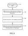
- FIG. 8is a flow diagram illustrating a method of providing interference compensating based on a detected common-mode signal.
- FIG. 8an exemplary noise canceling operation of transceiver 400 is now described.
- a differential signalis generated by differential driver 434 for transmission ( 810 ).
- the differential signalAfter experiencing noise interference in the interface circuitry 410 , the differential signal becomes distorted (not shown in FIG. 4 for simplicity), and the distortion is picked up by common mode signal detection circuit 420 ( 820 ).
- the distortionthen forms a common mode signal 450 on the center tap 428 of common mode signal detection circuit 420 , which in turn passes the common mode signal 450 to compensator circuit 430 via common mode path 424 .
- the control circuitry 432 in compensation circuit 430evaluates the common mode signal 450 ( 830 ), and adjusts a suitable part of the differential driver 434 to generate an adjusted differential signal 452 ( 840 ).
- the pattern of the common mode signal 450is latched until a new common mode signal pattern is detected by the common mode signal detection circuit 420 . Therefore, when the adjusted differential signal 452 travels through the interface circuitry 410 and is interfered by the same noise or imbalance, the interference becomes compensated by the adjustment. In this manner, when the adjusted differential signal 452 reaches transmission port 440 , the differential signal ready to be transmitted becomes a balanced differential signal 454 with a flat common mode signal.
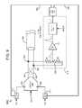
- FIG. 9illustrates one embodiment of a transmit circuit, generally designated 900 that detects and compensates for common mode signals due to timing imbalances between respective true and complement signal components of a differential signal.
- the transmit circuit 900is generally formed on an integrated circuit chip and includes a driver 902 that generates a differential signal having respective true and complement signal components onto respective output paths 903 and 905 .
- the driverincludes a data input to receive data DATA, and respective timing inputs at 907 and 909 to receive clock signals CK and /CK that are output from respective adjustable delay circuits 911 and 913 , where each clock delay circuit effectively delays either the signal rise or fall transition time at driver output.
- the driver 902may be embodied as a voltage-mode pseudo-differential multi-bit digital-to-analog converter (DAC). While only a single transmit circuit is shown for clarity purposes, a plurality of driver circuits may be provided on a single integrated circuit chip, and one or more of the circuits may employ separate common mode detection and compensation schemes, or share a detection and compensation circuit among several driver circuits.
- DACdigital-to-analog converter
- the true and complement componentshave the same amplitude, rise/fall time, and are exactly 180 degrees out of phase. In reality, imbalances may occur as a result of shifts in the timing of one component relative to the other, creating positive or negative common mode signals.
- the differential signalis driven to a transmission port that employs true and complement circuit pins or pads 904 and 906 that interface with a transmission medium, such as a multi-conductor cable 908 . Transmitted signals that exhibit undesirable levels of common mode may give rise to unacceptable levels of RF emissions as the signals propagate along the transmission medium 908 .
- a common mode detector 910that senses both components of the differential signal, and produces a signal indicative of the level of common mode associated with the differential signal.
- One embodiment of the detectorincludes matching impedance branches in the form of resistors R 1 and R 2 .
- the matching resistorsare configured as a voltage divider with a sensing branch coupled to the resistors at a sense node 912 . Any imbalance in voltage across the resistors is detected as a common mode signal and fed to a gain amplifier 914 .
- the gain amplifierboosts the level of the detected signal to full-scale for ease of detection.
- the boosted common mode signal output from the gain amplifier 914is fed to an accumulator circuit 916 .
- the accumulator circuittakes the form of an analog integrator 916 .
- the integratorgenerates an integration value based on the received waveform and accumulates the integration value with prior integrated values to form a running accumulation. This is seen more clearly in FIGS. 10A and 10B , where a differential signal waveform is superimposed in time with a common mode voltage waveform, and an integrated voltage waveform output from an integrator.
- the accumulation circuitmay take the form of a digital accumulator or counter to increment and or decrement depending on the polarity of the detected common mode signal.
- the output of the integrator 916is fed to a control unit 918 .
- control unit 918may be configured in a variety of ways to correct for detected common mode.
- the control unitmay be programmed with one or more threshold values that represent a maximum accumulated integration value. Other threshold parameters may also be utilized, including values detected over short or long signal transmission intervals.
- a comparator circuit(not shown) in the control unit compares incoming outputs from the integrator 916 to the threshold value. If the threshold value is exceeded, the control unit 918 generates a control signal that is applied to a selected control path 920 or 922 .
- the control pathsprovide feedback paths from the control unit 918 to the respective delay circuits 907 and 909 . Application of the control signal to one of the delay circuits causes a delay to the clock feeding the corresponding driver timing input.
- the delay circuitrymay be employed in the driver 902 to directly delay the differential signal rise or fall transition times with respect to each other (rather than delay the respective clocks for the signal components).
- FIGS. 10A and 10Billustrate waveforms that are generated by the transmit circuit described above, and superimposed along the same time scale to show interralationships therebetween.
- a differential signal Vdiffis shown with a true signal component 1002 and a complement signal component 1004 , where the signals rise times leads the fall times by a duration ⁇ t.
- the ⁇ tis thus a timing imbalance that gives rise to a level of common mode as the differential signal is transmitted.
- a detected “positive” common mode waveform Vcom due to the timing imbalanceis shown just underneath the differential waveform Vdiff, and shows small levels of signal over the duration of the timing imbalance ⁇ t.
- FIG. 10Billustrates similar waveforms where the signal rise time lags the fall time, resulting in a negative common mode Vcm waveform, and negative accumulation Vint.
- correcting imbalance in the differential signalmay occur in a training mode of operation.
- certain data patternsmay be fed from a transmit end of the link to the receiver end. Detecting the common mode with the above-described on-chip circuitry quickly allows for adjustment to the differential signal components to minimize the common mode, and thus reduce any undesirable RF emissions along the cable.
- an adaptive adjustment processmay be performed continuously or periodically during live data modes of operation.
- FIG. 11illustrates a further embodiment of a transmit circuit, generally designated 1100 .
- the transmit circuit 1100is similar to that shown in FIG. 9 , and includes a main driver circuit 1102 and a replica driver circuit 1104 .
- the main driver circuit 1102includes a driver 1106 that generates a differential signal for application to a medium such as a cable 1108 .
- the driverreceives live input data Tx DATA and has respective timing inputs at 1110 and 1112 responsive to outputs from delay circuits 1114 and 1116 that are driven by respective clock signals CK and /CK.
- the driveris embodied as a pseudo-differential 10-bit DAC.
- the replica driver circuit 1104includes a replica driver 1118 that includes circuitry substantially matched to that of the main driver 1106 . By “matched”, the circuitry generally exhibits drifting electrical parameters depending on temperature variations in the integrated circuit.
- the replica driver 1118may take the form of a sub-driver cell typically used as a most-significant-bit (MSB) of the main driver DAC.
- MSBmost-significant-bit
- the output of the replica driverfeeds a common mode detector circuit 1120 that is configured similar to that described in the transmit circuit 900 and shown in FIG. 9 .
- the common mode detector circuit 1120includes matched impedance branches R 3 and R 4 that feed a gain amplifier 1122 .
- An accumulator 1124 in the form of an analog integrator or digital countermonitors an aggregate level of detected common mode for application to a control unit 1126 .
- the control circuit 1126compares the incoming aggregated common mode from the detector 1120 , and if a predetermined threshold level is exceeded, generates a control signal to adjust delay circuits 1128 and 1130 that control the timing of the respective true and complement timing signals CK and /CK fed to the replica driver 1118 .
- the control signalis also fed to one or both of the delay circuits 1114 and/or 1116 associated with the main driver 1106 . Slight adjustments to one or both of the delay circuits 129 and/or 130 serve to adjust the detected imbalance causing the common mode. Subsequent detections may fine-tune the imbalance further to reduce the common mode levels to acceptable levels.
- the delay circuitrymay be configured to directly delay the differential component signals, rather than delay the clock signals.
- a replica circuit 1104 in the transmit circuit 1100enables the timing corrections to be carried out without interfering with signaling occurring over the cable 1108 . This may occur, for example, during 10 GBASE-T autonegotiation and/or other link initialization operation that involves data transmissions between link partners over the cable 1108 . Since the replica driver circuitry is matched to the main driver circuitry, and exhibits similar drift characteristics during temperature changes, adjustments to the replica delay circuits will have an equal effect on the main driver 1106 when the adjustments are applied to the main driver delay circuits 1114 and 1116 .
- signals described or depicted as having active-high or active-low logic levelsmay have opposite logic levels in alternative embodiments.
- Component circuitry within integrated circuit devicesmay be implemented using metal oxide semiconductor (MOS) technology, bipolar technology or any other technology in which logical and analog circuits may be implemented.
- MOSmetal oxide semiconductor
- a signalis said to be “asserted” when the signal is driven to a low or high logic state (or charged to a high logic state or discharged to a low logic state) to indicate a particular condition.
- a signalis said to be “deasserted” to indicate that the signal is driven (or charged or discharged) to a state other than the asserted state (including a high or low logic state, or the floating state that may occur when the signal driving circuit is transitioned to a high impedance condition, such as an open drain or open collector condition).
- a signal driving circuitis said to “output” a signal to a signal receiving circuit when the signal driving circuit asserts (or deasserts, if explicitly stated or indicated by context) the signal on a signal line coupled between the signal driving and signal receiving circuits.
- a signal lineis said to be “activated” when a signal is asserted on the signal line, and “deactivated” when the signal is deasserted.
- the prefix symbol “/” attached to signal namesindicates that the signal is an active low signal (i.e., the asserted state is a logic low state).
- a line over a signal namee.g., ‘ ⁇ signal name> ’ is also used to indicate an active low signal.
- the term “coupled”is used herein to express a direct connection as well as a connection through one or more intervening circuits or structures.
- Integrated circuit device “programming”may include, for example and without limitation, loading a control value into a register or other storage circuit within the device in response to a host instruction and thus controlling an operational aspect of the device, establishing a device configuration or controlling an operational aspect of the device through a one-time programming operation (e.g., blowing fuses within a configuration circuit during device production), and/or connecting one or more selected pins or other contact structures of the device to reference voltage lines (also referred to as strapping) to establish a particular device configuration or operation aspect of the device.
- a one-time programming operatione.g., blowing fuses within a configuration circuit during device production
- reference voltage linesalso referred to as strapping
Landscapes
- Engineering & Computer Science (AREA)
- Computer Networks & Wireless Communication (AREA)
- Signal Processing (AREA)
- Power Engineering (AREA)
- Dc Digital Transmission (AREA)
Abstract
Description
Claims (20)
Priority Applications (1)
| Application Number | Priority Date | Filing Date | Title |
|---|---|---|---|
| US13/790,333US8891595B1 (en) | 2010-05-28 | 2013-03-08 | Electromagnetic interference reduction in wireline applications using differential signal compensation |
Applications Claiming Priority (3)
| Application Number | Priority Date | Filing Date | Title |
|---|---|---|---|
| US34949210P | 2010-05-28 | 2010-05-28 | |
| US13/111,785US8724678B2 (en) | 2010-05-28 | 2011-05-19 | Electromagnetic interference reduction in wireline applications using differential signal compensation |
| US13/790,333US8891595B1 (en) | 2010-05-28 | 2013-03-08 | Electromagnetic interference reduction in wireline applications using differential signal compensation |
Related Parent Applications (1)
| Application Number | Title | Priority Date | Filing Date |
|---|---|---|---|
| US13/111,785Continuation-In-PartUS8724678B2 (en) | 2010-05-28 | 2011-05-19 | Electromagnetic interference reduction in wireline applications using differential signal compensation |
Publications (1)
| Publication Number | Publication Date |
|---|---|
| US8891595B1true US8891595B1 (en) | 2014-11-18 |
Family
ID=51870192
Family Applications (1)
| Application Number | Title | Priority Date | Filing Date |
|---|---|---|---|
| US13/790,333Active2031-05-26US8891595B1 (en) | 2010-05-28 | 2013-03-08 | Electromagnetic interference reduction in wireline applications using differential signal compensation |
Country Status (1)
| Country | Link |
|---|---|
| US (1) | US8891595B1 (en) |
Cited By (15)
| Publication number | Priority date | Publication date | Assignee | Title |
|---|---|---|---|---|
| US20140205027A1 (en)* | 2011-08-23 | 2014-07-24 | Nec Corporation | Communication apparatus, signal superimposing circuit, and method for superimposing signals |
| US20150304138A1 (en)* | 2013-07-18 | 2015-10-22 | Funai Electric Co., Ltd. | Electronic device and signal transmission method |
| US20160218768A1 (en)* | 2015-01-22 | 2016-07-28 | Airoha Technology Corp. | Circuit of wireless transceiver chip |
| WO2017140884A1 (en)* | 2016-02-18 | 2017-08-24 | Elmos Semiconductor Aktiengesellschaft | Method for increasing the signal-to-noise ratio for common-mode interference on a two-wire data bus |
| US20170279345A1 (en)* | 2016-03-22 | 2017-09-28 | Infineon Technologies Ag | Active common mode cancellation |
| US20180224515A1 (en)* | 2017-02-06 | 2018-08-09 | Tektronix, Inc. | Calibration for Common Mode Current |
| US10120406B1 (en)* | 2017-04-27 | 2018-11-06 | Microchip Technology Incorporated | Adaptive common mode dimmer |
| US20190199400A1 (en)* | 2017-12-21 | 2019-06-27 | Nxp B.V. | Transceiver and method of adjusting the tx signal of the transceiver for weakening emi |
| CN110118899A (en)* | 2018-02-07 | 2019-08-13 | 亚德诺半导体无限责任公司 | Detect the fault state and the unbalanced method and apparatus of channel of differential signal chain |
| EP3524988A1 (en)* | 2018-02-07 | 2019-08-14 | Analog Devices Global Unlimited Company | A method of and apparatus for detecting open circuit or other failure conditions at an input to a signal chain and for detecting channel imbalance in a differential signal chain |
| US10594363B2 (en) | 2017-12-21 | 2020-03-17 | Nxp B.V. | Electromagnetic emission detection, transceiver and system |
| CN113536719A (en)* | 2020-04-13 | 2021-10-22 | 联合汽车电子有限公司 | PCB simulation circuit and PCB simulation circuit analysis method |
| WO2023151811A1 (en)* | 2022-02-11 | 2023-08-17 | Huawei Technologies Co., Ltd. | Apparatus and method for reduction of common mode signal in wired data communication link |
| US20230291424A1 (en)* | 2019-09-09 | 2023-09-14 | Everactive, Inc. | Wireless receiver apparatus and method |
| US12282045B2 (en) | 2022-12-02 | 2025-04-22 | Infineon Technologies Ag | Common mode evaluation in a differential galvanic isolation signal transmission circuit |
Citations (106)
| Publication number | Priority date | Publication date | Assignee | Title |
|---|---|---|---|---|
| US3506906A (en) | 1967-12-18 | 1970-04-14 | Rucker Co | Ground fault circuit interrupter with inadvertent ground sensor |
| US3671859A (en) | 1970-11-04 | 1972-06-20 | Gen Electric | Frequency transducer |
| US4797902A (en) | 1984-12-29 | 1989-01-10 | Sony Corporation | Digital signal transmission device |
| US4870370A (en) | 1988-02-19 | 1989-09-26 | Silicon Systems, Inc. | Method and apparatus for two stage automatic gain control |
| US5157690A (en) | 1990-10-30 | 1992-10-20 | Level One Communications, Inc. | Adaptive convergent decision feedback equalizer |
| US5283811A (en) | 1991-09-03 | 1994-02-01 | General Electric Company | Decision feedback equalization for digital cellular radio |
| US5550924A (en) | 1993-07-07 | 1996-08-27 | Picturetel Corporation | Reduction of background noise for speech enhancement |
| WO1997040587A1 (en) | 1996-04-19 | 1997-10-30 | Amati Communications Corporation | Radio frequency noise canceller |
| US5777692A (en) | 1994-12-29 | 1998-07-07 | Philips Electronics North America Corporation | Receiver based methods and devices for combating co-channel NTSC interference in digital transmission |
| US5832032A (en) | 1995-11-09 | 1998-11-03 | Northern Telecom Limited | Interference reduction in telecommunications systems |
| US5889511A (en) | 1997-01-17 | 1999-03-30 | Tritech Microelectronics International, Ltd. | Method and system for noise reduction for digitizing devices |
| US5910960A (en) | 1995-06-07 | 1999-06-08 | Discovision Associates | Signal processing apparatus and method |
| US5995566A (en) | 1995-11-04 | 1999-11-30 | Northern Telecom Limited | Interference reduction in telecommunication systems |
| US6011508A (en) | 1997-10-31 | 2000-01-04 | Magnemotion, Inc. | Accurate position-sensing and communications for guideway operated vehicles |
| US6035360A (en) | 1997-10-29 | 2000-03-07 | International Business Machines Corporation | Multi-port SRAM access control using time division multiplexed arbitration |
| US6052420A (en) | 1997-05-15 | 2000-04-18 | Northern Telecom Limited | Adaptive multiple sub-band common-mode RFI suppression |
| US6069917A (en) | 1997-05-23 | 2000-05-30 | Lucent Technologies Inc. | Blind training of a decision feedback equalizer |
| US6285718B1 (en) | 1997-02-28 | 2001-09-04 | Orckit Communication Ltd. | Adaptive noise canceller |
| US6385315B1 (en) | 1998-06-05 | 2002-05-07 | Mphase Corporation | Video voice separation system |
| US6424234B1 (en) | 1998-09-18 | 2002-07-23 | Greatbatch-Sierra, Inc. | Electromagnetic interference (emi) filter and process for providing electromagnetic compatibility of an electronic device while in the presence of an electromagnetic emitter operating at the same frequency |
| US6486746B1 (en) | 2000-06-30 | 2002-11-26 | Intel Corporation | Termination circuit for decoupling unused wires on a network device's unshielded twisted pair (UTP) cable |
| US20030186591A1 (en) | 1993-03-12 | 2003-10-02 | Cekan/Cdt A/S | Connector element for high-speed data communications |
| US20030223488A1 (en) | 2002-04-04 | 2003-12-04 | Chunlin Li | Fast phase synchronization and retrieval of sequence components in three-phase networks |
| US20030223505A1 (en) | 1999-12-30 | 2003-12-04 | Rami Verbin | Data transceiver with filtering and precoding |
| US20040010203A1 (en) | 2002-07-12 | 2004-01-15 | Bionova Technologies Inc. | Method and apparatus for the estimation of anesthetic depth using wavelet analysis of the electroencephalogram |
| US6683913B1 (en) | 1999-12-30 | 2004-01-27 | Tioga Technologies Inc. | Narrowband noise canceller |
| US20040023631A1 (en) | 2002-07-30 | 2004-02-05 | Deutsch Jeffrey T. | Method and system for rejecting noise in information communication |
| US6690739B1 (en) | 2000-01-14 | 2004-02-10 | Shou Yee Mui | Method for intersymbol interference compensation |
| US6711207B1 (en) | 1999-03-11 | 2004-03-23 | Globespanvirata, Inc. | System and method for reduced power consumption in digital subscriber line modems |
| US6734659B1 (en) | 2002-06-13 | 2004-05-11 | Mykrolis Corporation | Electronic interface for use with dual electrode capacitance diaphragm gauges |
| US6771720B1 (en) | 2001-03-30 | 2004-08-03 | Skyworks Solutions, Inc. | Amplification control scheme for a receiver |
| US20040164619A1 (en) | 2003-02-21 | 2004-08-26 | Parker Timothy J. | Connector module with embedded Power-Over-Ethernet functionality |
| US20040213366A1 (en) | 2002-07-02 | 2004-10-28 | Pioneer Corporation | Receiver with adjacent interfering wave elimination function |
| US20040239465A1 (en) | 2003-05-21 | 2004-12-02 | Bel Fuse, Inc. | LAN magnetic interface circuit |
| US20040252755A1 (en) | 1999-08-13 | 2004-12-16 | Broadcom Corporation | Decision feedback equalizer and precoder ramping circuit |
| US20040257743A1 (en) | 2003-06-19 | 2004-12-23 | Bel-Fuse, Inc. | LAN magnetic interface circuit with passive ESD protection |
| US20050018777A1 (en) | 2003-01-28 | 2005-01-27 | Kameran Azadet | Method and apparatus for reducing noise in an unbalanced channel using common mode component |
| US20050025266A1 (en) | 1998-11-11 | 2005-02-03 | Chan Kevin T. | Adaptive electronic transmission signal cancellation apparatus for full duplex communication |
| US20050053229A1 (en) | 2003-09-08 | 2005-03-10 | Tsatsanis Michail Konstantinos | Common mode noise cancellation |
| US20050097218A1 (en) | 2003-10-03 | 2005-05-05 | Dell Products L.P. | System, method & device for tuning a switched transmission line for ethernet local area network-on-motherboard (LOM) |
| US20050123081A1 (en) | 2003-12-05 | 2005-06-09 | Ramin Shirani | Low-power mixed-mode echo/crosstalk cancellation in wireline communications |
| US20050135489A1 (en) | 2003-12-17 | 2005-06-23 | Andrew Ho | Noise-tolerant signaling schemes supporting simplified timing and data recovery |
| US6924724B2 (en) | 2003-01-24 | 2005-08-02 | Solarflare Communications, Inc. | Method and apparatus for transformer bandwidth enhancement |
| US6934345B2 (en) | 2001-01-17 | 2005-08-23 | Adtran, Inc. | Apparatus, method and system for correlated noise reduction in a trellis coded environment |
| US20050203744A1 (en) | 2004-03-11 | 2005-09-15 | Denso Corporation | Method, device and program for extracting and recognizing voice |
| US6959056B2 (en) | 2000-06-09 | 2005-10-25 | Bell Canada | RFI canceller using narrowband and wideband noise estimators |
| US20050243483A1 (en) | 2004-04-28 | 2005-11-03 | Bel-Fuse | Differential electrical surge protection within a LAN magnetics interface circuit |
| US20060018388A1 (en) | 1998-10-30 | 2006-01-26 | Chan Kevin T | Reduction of aggregate EMI emissions of multiple transmitters |
| US6999504B1 (en) | 2000-11-21 | 2006-02-14 | Globespanvirata, Inc. | System and method for canceling crosstalk |
| US20060056503A1 (en) | 2004-09-13 | 2006-03-16 | Regents Of The University Of Minnesota | Pipelined parallel decision feedback decoders for high-speed communication systems |
| US7026730B1 (en) | 2002-12-20 | 2006-04-11 | Cisco Technology, Inc. | Integrated connector unit |
| US7031402B2 (en) | 2001-06-12 | 2006-04-18 | Hitachi Kokusai Electric Inc. | Interference signal removal system |
| US20060159186A1 (en) | 2005-01-14 | 2006-07-20 | Piping Hot Networks Limited | Data, power and supervisory signaling over twisted pairs |
| US20060182014A1 (en) | 2005-02-14 | 2006-08-17 | Texas Instruments Incorporated | Apparatus for and method of characterization of ethernet cable impairments |
| US7103013B1 (en) | 2001-11-20 | 2006-09-05 | Silicon Image | Bidirectional bridge circuit having high common mode rejection and high input sensitivity |
| US20060256880A1 (en) | 2005-05-13 | 2006-11-16 | Frisch Arnold M | Automatic skew correction for differential signals |
| US7164764B2 (en) | 2002-11-07 | 2007-01-16 | Solarflare Communications, Inc. | Method and apparatus for precode crosstalk mitigation |
| US20070014378A1 (en) | 2005-07-13 | 2007-01-18 | Leanics Corporation | System and method for MIMO equalization for DSP transceivers |
| US7173992B2 (en) | 2001-12-11 | 2007-02-06 | Sasken Communication Technologies Limited | Method for synchronization in wireless systems using receive diversity |
| US20070081475A1 (en) | 2005-10-11 | 2007-04-12 | Teranetics, Inc. | Multiple modulation rate 10Gbase-T transmission |
| US20070146011A1 (en) | 2005-12-28 | 2007-06-28 | O'mahony Frank P | Duty cycle adjustment |
| US20070192505A1 (en) | 2006-02-13 | 2007-08-16 | Teranetics, Inc. | Auto-sequencing transmission speed of a data port |
| US20070258517A1 (en) | 2006-05-08 | 2007-11-08 | Micro Circuits Corporation | Adaptive error slicer and residual intersymbol interference estimator |
| US20070280388A1 (en) | 2006-05-31 | 2007-12-06 | Texas Instruments Incorporated | Apparatus for and method of canceller tap shutdown in a communication system |
| US7333603B1 (en) | 2000-05-12 | 2008-02-19 | National Semiconductor Corporation | System and method for adapting an analog echo canceller in a transceiver front end |
| USRE40149E1 (en) | 1999-12-30 | 2008-03-11 | Stmicroelectronics, N.V. | Method and apparatus for RF common-mode noise rejection in a DSL receiver |
| US20080089433A1 (en) | 2006-10-13 | 2008-04-17 | Jun Hyok Cho | Method and apparatus for adapting to dynamic channel conditions in a multi-channel communication system |
| US20080095283A1 (en) | 2006-10-19 | 2008-04-24 | Ehud Shoor | Techniques to reduce the impact of jitter on communications system performance |
| US20080107167A1 (en) | 2006-11-03 | 2008-05-08 | Hsu-Jung Tung | Data recovery apparatus and method |
| US20080160915A1 (en) | 2006-12-29 | 2008-07-03 | Texas Instruments Incorporated | Far-end crosstalk (fext) canceller |
| US20080198909A1 (en) | 2003-09-08 | 2008-08-21 | Michail Konstantinos Tsatsanis | Efficient multiple input multiple output signal processing method and apparatus |
| US20080267212A1 (en) | 2007-04-24 | 2008-10-30 | Philip John Crawley | Isolated Ethernet Physical Layer (PHY) |
| US7457386B1 (en) | 2000-05-12 | 2008-11-25 | National Semiconductor Corporation | System and method for cancelling signal echoes in a full-duplex transceiver front end |
| US7459982B2 (en) | 2006-09-27 | 2008-12-02 | Finisar Corporation | EMI reduction stage in a post-amplifier |
| US20090061808A1 (en) | 2007-08-28 | 2009-03-05 | Higgins Robert P | Adaptive rf canceller system and method |
| US20090097539A1 (en) | 2007-10-12 | 2009-04-16 | Harris Corporation | Communications system using adaptive filter and variable delay before adaptive filter taps |
| US20090097401A1 (en) | 2007-10-12 | 2009-04-16 | Wael William Diab | Method and system for configurable data rate thresholds for energy efficient ethernet |
| US7522928B2 (en) | 2003-10-24 | 2009-04-21 | Intel Corporation | Dynamic EMI (electromagnetic interference) management |
| US7542528B1 (en) | 2004-08-10 | 2009-06-02 | Marvell International Ltd. | Far end crosstalk mitigation in multiple-input multiple-output (MIMO) channels using partial maximum likelihood MIMO-DFE |
| US20090154455A1 (en) | 2007-12-17 | 2009-06-18 | Wael William Diab | Method And System For Near Continuous Data Rate Limit Adjustment Via A Plurality Of Link Variables In An Energy Efficient Network |
| US20090161781A1 (en) | 2007-12-21 | 2009-06-25 | Broadcom Corporation | Characterizing channel response using data tone decision feedback |
| US7593470B2 (en)* | 1999-08-11 | 2009-09-22 | Rambus Inc. | High-speed communication system with a feedback synchronization loop |
| US7634032B2 (en) | 2004-03-04 | 2009-12-15 | Adtran, Inc. | System and method for detecting non-linear distortion of signals communicated across telecommunication lines |
| US20100046543A1 (en) | 2008-08-11 | 2010-02-25 | Gavin Parnaby | Method of synchronization for low power idle |
| US20100073072A1 (en) | 2008-09-24 | 2010-03-25 | Sony Ericsson Mobile Communications Ab | Biasing arrangement, electronic apparatus, biasing method, and computer program |
| US20100074310A1 (en) | 2000-07-31 | 2010-03-25 | Pierte Roo | Active resistive summer for a transformer hybrid |
| US20100086019A1 (en) | 1998-11-13 | 2010-04-08 | Agazzi Oscar E | High-Speed Decoder for a Multi-Pair Gigabit Transceiver |
| US7706434B1 (en) | 2005-04-15 | 2010-04-27 | Aquantia Corporation | Method and apparatus for cancelling interference in a communication system |
| US7708595B2 (en) | 2008-09-10 | 2010-05-04 | Hon Hai Precision Ind. Co., Ltd. | Electrical connector system with magnetic module |
| US20100111202A1 (en) | 2008-10-30 | 2010-05-06 | Schley-May James T | Method and apparatus for generating a common-mode reference signal |
| US20100159866A1 (en) | 2008-12-23 | 2010-06-24 | Fudge Gerald L | Systems and methods for interference cancellation |
| US20110032048A1 (en) | 2009-08-10 | 2011-02-10 | National Taiwan University | Filtering device and differential signal transmission circuit capable of suppressing common-mode noises upon transmission of a deifferential signal |
| US7906994B2 (en)* | 2009-02-24 | 2011-03-15 | Standard Microsystems Corporation | Fast common mode feedback control for differential driver |
| US20110069794A1 (en) | 2009-09-18 | 2011-03-24 | Mehdi Tavassoli Kilani | Method and system for interference cancellation |
| US20110106459A1 (en) | 2009-10-29 | 2011-05-05 | Northrop Grumman Corporation | In-situ optical crack measurement using a dot pattern |
| WO2011056970A2 (en) | 2009-11-06 | 2011-05-12 | Molex Incorporated | Mag-jack module |
| US20110212692A1 (en) | 2010-02-26 | 2011-09-01 | Intersil Americas Inc. | Cascaded Filter Based Noise and Interference Canceller |
| US8022728B2 (en)* | 2005-09-16 | 2011-09-20 | Fujitsu Limited | Common-mode voltage controller |
| US20110256857A1 (en) | 2010-04-20 | 2011-10-20 | Intersil Americas Inc. | Systems and Methods for Improving Antenna Isolation Using Signal Cancellation |
| US20110293041A1 (en) | 2010-05-25 | 2011-12-01 | Lei Luo | Receiver Resistor Network for Common-Mode Signaling |
| US20110296267A1 (en) | 2010-05-28 | 2011-12-01 | Teranetics, Inc. | Reducing Electromagnetic Interference in a Received Signal |
| US8094546B2 (en) | 2007-06-13 | 2012-01-10 | Lantiq Deutschland Gmbh | Device and method for compensating crosstalk in transmission links |
| US8139602B2 (en) | 2004-07-28 | 2012-03-20 | Rockstar Bidco, LP | System, method and device for high bit rate data communication over twisted pair cables |
| US8331508B2 (en) | 2010-07-14 | 2012-12-11 | Applied Micro Circuits Corporation | Narrowband interference cancellation method and circuit |
| US8625704B1 (en) | 2008-09-25 | 2014-01-07 | Aquantia Corporation | Rejecting RF interference in communication systems |
| US8724678B2 (en)* | 2010-05-28 | 2014-05-13 | Aquantia Corporation | Electromagnetic interference reduction in wireline applications using differential signal compensation |
- 2013
- 2013-03-08USUS13/790,333patent/US8891595B1/enactiveActive
Patent Citations (115)
| Publication number | Priority date | Publication date | Assignee | Title |
|---|---|---|---|---|
| US3506906A (en) | 1967-12-18 | 1970-04-14 | Rucker Co | Ground fault circuit interrupter with inadvertent ground sensor |
| US3671859A (en) | 1970-11-04 | 1972-06-20 | Gen Electric | Frequency transducer |
| US4797902A (en) | 1984-12-29 | 1989-01-10 | Sony Corporation | Digital signal transmission device |
| US4870370A (en) | 1988-02-19 | 1989-09-26 | Silicon Systems, Inc. | Method and apparatus for two stage automatic gain control |
| US5157690A (en) | 1990-10-30 | 1992-10-20 | Level One Communications, Inc. | Adaptive convergent decision feedback equalizer |
| US5283811A (en) | 1991-09-03 | 1994-02-01 | General Electric Company | Decision feedback equalization for digital cellular radio |
| US20030186591A1 (en) | 1993-03-12 | 2003-10-02 | Cekan/Cdt A/S | Connector element for high-speed data communications |
| US5550924A (en) | 1993-07-07 | 1996-08-27 | Picturetel Corporation | Reduction of background noise for speech enhancement |
| US5777692A (en) | 1994-12-29 | 1998-07-07 | Philips Electronics North America Corporation | Receiver based methods and devices for combating co-channel NTSC interference in digital transmission |
| US5910960A (en) | 1995-06-07 | 1999-06-08 | Discovision Associates | Signal processing apparatus and method |
| US5995566A (en) | 1995-11-04 | 1999-11-30 | Northern Telecom Limited | Interference reduction in telecommunication systems |
| US5832032A (en) | 1995-11-09 | 1998-11-03 | Northern Telecom Limited | Interference reduction in telecommunications systems |
| US5995567A (en) | 1996-04-19 | 1999-11-30 | Texas Instruments Incorporated | Radio frequency noise canceller |
| WO1997040587A1 (en) | 1996-04-19 | 1997-10-30 | Amati Communications Corporation | Radio frequency noise canceller |
| US5889511A (en) | 1997-01-17 | 1999-03-30 | Tritech Microelectronics International, Ltd. | Method and system for noise reduction for digitizing devices |
| US6285718B1 (en) | 1997-02-28 | 2001-09-04 | Orckit Communication Ltd. | Adaptive noise canceller |
| US6052420A (en) | 1997-05-15 | 2000-04-18 | Northern Telecom Limited | Adaptive multiple sub-band common-mode RFI suppression |
| US6069917A (en) | 1997-05-23 | 2000-05-30 | Lucent Technologies Inc. | Blind training of a decision feedback equalizer |
| US6035360A (en) | 1997-10-29 | 2000-03-07 | International Business Machines Corporation | Multi-port SRAM access control using time division multiplexed arbitration |
| US6011508A (en) | 1997-10-31 | 2000-01-04 | Magnemotion, Inc. | Accurate position-sensing and communications for guideway operated vehicles |
| US6385315B1 (en) | 1998-06-05 | 2002-05-07 | Mphase Corporation | Video voice separation system |
| US6424234B1 (en) | 1998-09-18 | 2002-07-23 | Greatbatch-Sierra, Inc. | Electromagnetic interference (emi) filter and process for providing electromagnetic compatibility of an electronic device while in the presence of an electromagnetic emitter operating at the same frequency |
| US20060018388A1 (en) | 1998-10-30 | 2006-01-26 | Chan Kevin T | Reduction of aggregate EMI emissions of multiple transmitters |
| US7492840B2 (en) | 1998-11-11 | 2009-02-17 | Broadcom Corporation | Adaptive electronic transmission signal cancellation apparatus for full duplex communication |
| US20050025266A1 (en) | 1998-11-11 | 2005-02-03 | Chan Kevin T. | Adaptive electronic transmission signal cancellation apparatus for full duplex communication |
| US20100086019A1 (en) | 1998-11-13 | 2010-04-08 | Agazzi Oscar E | High-Speed Decoder for a Multi-Pair Gigabit Transceiver |
| US6711207B1 (en) | 1999-03-11 | 2004-03-23 | Globespanvirata, Inc. | System and method for reduced power consumption in digital subscriber line modems |
| US7593470B2 (en)* | 1999-08-11 | 2009-09-22 | Rambus Inc. | High-speed communication system with a feedback synchronization loop |
| US20040252755A1 (en) | 1999-08-13 | 2004-12-16 | Broadcom Corporation | Decision feedback equalizer and precoder ramping circuit |
| US6683913B1 (en) | 1999-12-30 | 2004-01-27 | Tioga Technologies Inc. | Narrowband noise canceller |
| USRE40149E1 (en) | 1999-12-30 | 2008-03-11 | Stmicroelectronics, N.V. | Method and apparatus for RF common-mode noise rejection in a DSL receiver |
| US20030223505A1 (en) | 1999-12-30 | 2003-12-04 | Rami Verbin | Data transceiver with filtering and precoding |
| US7200180B2 (en) | 1999-12-30 | 2007-04-03 | Tioga Technologies, Inc. | Data transceiver with filtering and precoding |
| US6690739B1 (en) | 2000-01-14 | 2004-02-10 | Shou Yee Mui | Method for intersymbol interference compensation |
| US7457386B1 (en) | 2000-05-12 | 2008-11-25 | National Semiconductor Corporation | System and method for cancelling signal echoes in a full-duplex transceiver front end |
| US7333603B1 (en) | 2000-05-12 | 2008-02-19 | National Semiconductor Corporation | System and method for adapting an analog echo canceller in a transceiver front end |
| US6959056B2 (en) | 2000-06-09 | 2005-10-25 | Bell Canada | RFI canceller using narrowband and wideband noise estimators |
| US6486746B1 (en) | 2000-06-30 | 2002-11-26 | Intel Corporation | Termination circuit for decoupling unused wires on a network device's unshielded twisted pair (UTP) cable |
| US20100074310A1 (en) | 2000-07-31 | 2010-03-25 | Pierte Roo | Active resistive summer for a transformer hybrid |
| US6999504B1 (en) | 2000-11-21 | 2006-02-14 | Globespanvirata, Inc. | System and method for canceling crosstalk |
| US6934345B2 (en) | 2001-01-17 | 2005-08-23 | Adtran, Inc. | Apparatus, method and system for correlated noise reduction in a trellis coded environment |
| US6771720B1 (en) | 2001-03-30 | 2004-08-03 | Skyworks Solutions, Inc. | Amplification control scheme for a receiver |
| US7031402B2 (en) | 2001-06-12 | 2006-04-18 | Hitachi Kokusai Electric Inc. | Interference signal removal system |
| US7103013B1 (en) | 2001-11-20 | 2006-09-05 | Silicon Image | Bidirectional bridge circuit having high common mode rejection and high input sensitivity |
| US7173992B2 (en) | 2001-12-11 | 2007-02-06 | Sasken Communication Technologies Limited | Method for synchronization in wireless systems using receive diversity |
| US7180940B2 (en) | 2002-04-04 | 2007-02-20 | Chunlin Li | Fast phase synchronization and retrieval of sequence components in three-phase networks |
| US20030223488A1 (en) | 2002-04-04 | 2003-12-04 | Chunlin Li | Fast phase synchronization and retrieval of sequence components in three-phase networks |
| US6734659B1 (en) | 2002-06-13 | 2004-05-11 | Mykrolis Corporation | Electronic interface for use with dual electrode capacitance diaphragm gauges |
| US20040213366A1 (en) | 2002-07-02 | 2004-10-28 | Pioneer Corporation | Receiver with adjacent interfering wave elimination function |
| US20040010203A1 (en) | 2002-07-12 | 2004-01-15 | Bionova Technologies Inc. | Method and apparatus for the estimation of anesthetic depth using wavelet analysis of the electroencephalogram |
| US20040023631A1 (en) | 2002-07-30 | 2004-02-05 | Deutsch Jeffrey T. | Method and system for rejecting noise in information communication |
| US7164764B2 (en) | 2002-11-07 | 2007-01-16 | Solarflare Communications, Inc. | Method and apparatus for precode crosstalk mitigation |
| US7026730B1 (en) | 2002-12-20 | 2006-04-11 | Cisco Technology, Inc. | Integrated connector unit |
| US6924724B2 (en) | 2003-01-24 | 2005-08-02 | Solarflare Communications, Inc. | Method and apparatus for transformer bandwidth enhancement |
| US20050018777A1 (en) | 2003-01-28 | 2005-01-27 | Kameran Azadet | Method and apparatus for reducing noise in an unbalanced channel using common mode component |
| US20040164619A1 (en) | 2003-02-21 | 2004-08-26 | Parker Timothy J. | Connector module with embedded Power-Over-Ethernet functionality |
| US7123117B2 (en) | 2003-05-21 | 2006-10-17 | Bel-Fuse Inc. | LAN magnetic interface circuit |
| US20040239465A1 (en) | 2003-05-21 | 2004-12-02 | Bel Fuse, Inc. | LAN magnetic interface circuit |
| US20040257743A1 (en) | 2003-06-19 | 2004-12-23 | Bel-Fuse, Inc. | LAN magnetic interface circuit with passive ESD protection |
| US20080198909A1 (en) | 2003-09-08 | 2008-08-21 | Michail Konstantinos Tsatsanis | Efficient multiple input multiple output signal processing method and apparatus |
| US20050053229A1 (en) | 2003-09-08 | 2005-03-10 | Tsatsanis Michail Konstantinos | Common mode noise cancellation |
| US7315592B2 (en) | 2003-09-08 | 2008-01-01 | Aktino, Inc. | Common mode noise cancellation |
| US20050097218A1 (en) | 2003-10-03 | 2005-05-05 | Dell Products L.P. | System, method & device for tuning a switched transmission line for ethernet local area network-on-motherboard (LOM) |
| US7522928B2 (en) | 2003-10-24 | 2009-04-21 | Intel Corporation | Dynamic EMI (electromagnetic interference) management |
| US20050123081A1 (en) | 2003-12-05 | 2005-06-09 | Ramin Shirani | Low-power mixed-mode echo/crosstalk cancellation in wireline communications |
| US20050135489A1 (en) | 2003-12-17 | 2005-06-23 | Andrew Ho | Noise-tolerant signaling schemes supporting simplified timing and data recovery |
| US7634032B2 (en) | 2004-03-04 | 2009-12-15 | Adtran, Inc. | System and method for detecting non-linear distortion of signals communicated across telecommunication lines |
| US20050203744A1 (en) | 2004-03-11 | 2005-09-15 | Denso Corporation | Method, device and program for extracting and recognizing voice |
| US7440892B2 (en) | 2004-03-11 | 2008-10-21 | Denso Corporation | Method, device and program for extracting and recognizing voice |
| US20050243483A1 (en) | 2004-04-28 | 2005-11-03 | Bel-Fuse | Differential electrical surge protection within a LAN magnetics interface circuit |
| US8139602B2 (en) | 2004-07-28 | 2012-03-20 | Rockstar Bidco, LP | System, method and device for high bit rate data communication over twisted pair cables |
| US7542528B1 (en) | 2004-08-10 | 2009-06-02 | Marvell International Ltd. | Far end crosstalk mitigation in multiple-input multiple-output (MIMO) channels using partial maximum likelihood MIMO-DFE |
| US20060056503A1 (en) | 2004-09-13 | 2006-03-16 | Regents Of The University Of Minnesota | Pipelined parallel decision feedback decoders for high-speed communication systems |
| US7656956B2 (en) | 2005-01-14 | 2010-02-02 | Motorola, Inc. | Data, power and supervisory signaling over twisted pairs |
| US20060159186A1 (en) | 2005-01-14 | 2006-07-20 | Piping Hot Networks Limited | Data, power and supervisory signaling over twisted pairs |
| US20060182014A1 (en) | 2005-02-14 | 2006-08-17 | Texas Instruments Incorporated | Apparatus for and method of characterization of ethernet cable impairments |
| US7706434B1 (en) | 2005-04-15 | 2010-04-27 | Aquantia Corporation | Method and apparatus for cancelling interference in a communication system |
| US20060256880A1 (en) | 2005-05-13 | 2006-11-16 | Frisch Arnold M | Automatic skew correction for differential signals |
| US20070014378A1 (en) | 2005-07-13 | 2007-01-18 | Leanics Corporation | System and method for MIMO equalization for DSP transceivers |
| US8022728B2 (en)* | 2005-09-16 | 2011-09-20 | Fujitsu Limited | Common-mode voltage controller |
| US20070081475A1 (en) | 2005-10-11 | 2007-04-12 | Teranetics, Inc. | Multiple modulation rate 10Gbase-T transmission |
| US20070146011A1 (en) | 2005-12-28 | 2007-06-28 | O'mahony Frank P | Duty cycle adjustment |
| US20070192505A1 (en) | 2006-02-13 | 2007-08-16 | Teranetics, Inc. | Auto-sequencing transmission speed of a data port |
| US20070258517A1 (en) | 2006-05-08 | 2007-11-08 | Micro Circuits Corporation | Adaptive error slicer and residual intersymbol interference estimator |
| US20070280388A1 (en) | 2006-05-31 | 2007-12-06 | Texas Instruments Incorporated | Apparatus for and method of canceller tap shutdown in a communication system |
| US7459982B2 (en) | 2006-09-27 | 2008-12-02 | Finisar Corporation | EMI reduction stage in a post-amplifier |
| US20080089433A1 (en) | 2006-10-13 | 2008-04-17 | Jun Hyok Cho | Method and apparatus for adapting to dynamic channel conditions in a multi-channel communication system |
| US20080095283A1 (en) | 2006-10-19 | 2008-04-24 | Ehud Shoor | Techniques to reduce the impact of jitter on communications system performance |
| US20080107167A1 (en) | 2006-11-03 | 2008-05-08 | Hsu-Jung Tung | Data recovery apparatus and method |
| US20080160915A1 (en) | 2006-12-29 | 2008-07-03 | Texas Instruments Incorporated | Far-end crosstalk (fext) canceller |
| US20080267212A1 (en) | 2007-04-24 | 2008-10-30 | Philip John Crawley | Isolated Ethernet Physical Layer (PHY) |
| US8094546B2 (en) | 2007-06-13 | 2012-01-10 | Lantiq Deutschland Gmbh | Device and method for compensating crosstalk in transmission links |
| US20090061808A1 (en) | 2007-08-28 | 2009-03-05 | Higgins Robert P | Adaptive rf canceller system and method |
| US20090097401A1 (en) | 2007-10-12 | 2009-04-16 | Wael William Diab | Method and system for configurable data rate thresholds for energy efficient ethernet |
| US20090097539A1 (en) | 2007-10-12 | 2009-04-16 | Harris Corporation | Communications system using adaptive filter and variable delay before adaptive filter taps |
| US20090154455A1 (en) | 2007-12-17 | 2009-06-18 | Wael William Diab | Method And System For Near Continuous Data Rate Limit Adjustment Via A Plurality Of Link Variables In An Energy Efficient Network |
| US20090161781A1 (en) | 2007-12-21 | 2009-06-25 | Broadcom Corporation | Characterizing channel response using data tone decision feedback |
| US20100046543A1 (en) | 2008-08-11 | 2010-02-25 | Gavin Parnaby | Method of synchronization for low power idle |
| US7708595B2 (en) | 2008-09-10 | 2010-05-04 | Hon Hai Precision Ind. Co., Ltd. | Electrical connector system with magnetic module |
| US20100073072A1 (en) | 2008-09-24 | 2010-03-25 | Sony Ericsson Mobile Communications Ab | Biasing arrangement, electronic apparatus, biasing method, and computer program |
| US8625704B1 (en) | 2008-09-25 | 2014-01-07 | Aquantia Corporation | Rejecting RF interference in communication systems |
| US20100111202A1 (en) | 2008-10-30 | 2010-05-06 | Schley-May James T | Method and apparatus for generating a common-mode reference signal |
| US8472532B2 (en) | 2008-10-30 | 2013-06-25 | 2Wire, Inc. | Method and apparatus for generating a common-mode reference signal |
| US20100159866A1 (en) | 2008-12-23 | 2010-06-24 | Fudge Gerald L | Systems and methods for interference cancellation |
| US7906994B2 (en)* | 2009-02-24 | 2011-03-15 | Standard Microsystems Corporation | Fast common mode feedback control for differential driver |
| US20110032048A1 (en) | 2009-08-10 | 2011-02-10 | National Taiwan University | Filtering device and differential signal transmission circuit capable of suppressing common-mode noises upon transmission of a deifferential signal |
| US20110069794A1 (en) | 2009-09-18 | 2011-03-24 | Mehdi Tavassoli Kilani | Method and system for interference cancellation |
| US20110106459A1 (en) | 2009-10-29 | 2011-05-05 | Northrop Grumman Corporation | In-situ optical crack measurement using a dot pattern |
| WO2011056970A2 (en) | 2009-11-06 | 2011-05-12 | Molex Incorporated | Mag-jack module |
| US20110212692A1 (en) | 2010-02-26 | 2011-09-01 | Intersil Americas Inc. | Cascaded Filter Based Noise and Interference Canceller |
| US20110256857A1 (en) | 2010-04-20 | 2011-10-20 | Intersil Americas Inc. | Systems and Methods for Improving Antenna Isolation Using Signal Cancellation |
| US20110293041A1 (en) | 2010-05-25 | 2011-12-01 | Lei Luo | Receiver Resistor Network for Common-Mode Signaling |
| US20110296267A1 (en) | 2010-05-28 | 2011-12-01 | Teranetics, Inc. | Reducing Electromagnetic Interference in a Received Signal |
| US8724678B2 (en)* | 2010-05-28 | 2014-05-13 | Aquantia Corporation | Electromagnetic interference reduction in wireline applications using differential signal compensation |
| US8331508B2 (en) | 2010-07-14 | 2012-12-11 | Applied Micro Circuits Corporation | Narrowband interference cancellation method and circuit |
Non-Patent Citations (6)
| Title |
|---|
| U.S. Appl. No. 12/563,938, filed Sep. 21, 2009, Sedarat. |
| U.S. Appl. No. 12/604,323, filed Oct. 22, 2009, Sedarat et al. |
| U.S. Appl. No. 12/604,343, filed Oct. 22, 2009, Farjadrad et al. |
| U.S. Appl. No. 12/604,351, filed Oct. 22, 2009, Sedarat et al. |
| U.S. Appl. No. 12/604,358, filed Oct. 22, 2009, Sedarat et al. |
| U.S. Appl. No. 12/977,844, filed Dec. 23, 2010, Sedarat. |
Cited By (27)
| Publication number | Priority date | Publication date | Assignee | Title |
|---|---|---|---|---|
| US20140205027A1 (en)* | 2011-08-23 | 2014-07-24 | Nec Corporation | Communication apparatus, signal superimposing circuit, and method for superimposing signals |
| US9031139B2 (en)* | 2011-08-23 | 2015-05-12 | Nec Corporation | Communication apparatus, signal superimposing circuit, and method for superimposing signals |
| US20150304138A1 (en)* | 2013-07-18 | 2015-10-22 | Funai Electric Co., Ltd. | Electronic device and signal transmission method |
| US9742503B2 (en)* | 2013-07-18 | 2017-08-22 | Funai Electric Co., Ltd. | Electronic device and signal transmission method |
| US20160218768A1 (en)* | 2015-01-22 | 2016-07-28 | Airoha Technology Corp. | Circuit of wireless transceiver chip |
| US9525452B2 (en)* | 2015-01-22 | 2016-12-20 | Airoha Technology Corp. | Circuit of wireless transceiver chip |
| US10715362B2 (en) | 2016-02-18 | 2020-07-14 | Elmos Semiconductor Aktiengesellschaft | Method for increasing the signal-to-noise ratio for common-mode interference on a two-wire data bus |
| CN108781091A (en)* | 2016-02-18 | 2018-11-09 | 艾尔默斯半导体股份公司 | Increase method for the signal-to-noise ratio of the common mode interference of two-wire system data/address bus |
| CN108781091B (en)* | 2016-02-18 | 2021-06-29 | 艾尔默斯半导体股份公司 | Signal-to-noise ratio increasing method for common-mode interference of two-wire data bus |
| WO2017140884A1 (en)* | 2016-02-18 | 2017-08-24 | Elmos Semiconductor Aktiengesellschaft | Method for increasing the signal-to-noise ratio for common-mode interference on a two-wire data bus |
| US9800133B2 (en)* | 2016-03-22 | 2017-10-24 | Infineon Technologies Ag | Active common mode cancellation |
| US20170279345A1 (en)* | 2016-03-22 | 2017-09-28 | Infineon Technologies Ag | Active common mode cancellation |
| US10514434B2 (en)* | 2017-02-06 | 2019-12-24 | Keithley Instruments, Llc | Calibration for common mode current |
| US20180224515A1 (en)* | 2017-02-06 | 2018-08-09 | Tektronix, Inc. | Calibration for Common Mode Current |
| US10120406B1 (en)* | 2017-04-27 | 2018-11-06 | Microchip Technology Incorporated | Adaptive common mode dimmer |
| US10594363B2 (en) | 2017-12-21 | 2020-03-17 | Nxp B.V. | Electromagnetic emission detection, transceiver and system |
| US10790873B2 (en)* | 2017-12-21 | 2020-09-29 | Nxp B.V. | Transceiver and method of adjusting the TX signal of the transceiver for weakening EMI |
| US20190199400A1 (en)* | 2017-12-21 | 2019-06-27 | Nxp B.V. | Transceiver and method of adjusting the tx signal of the transceiver for weakening emi |
| US10476458B2 (en) | 2018-02-07 | 2019-11-12 | Analog Devices Global Unlimited Company | Method of and apparatus for detecting open circuit conditions at an input to a signal chain and for detecting channel imbalance in a differential signal chain |
| EP3524988A1 (en)* | 2018-02-07 | 2019-08-14 | Analog Devices Global Unlimited Company | A method of and apparatus for detecting open circuit or other failure conditions at an input to a signal chain and for detecting channel imbalance in a differential signal chain |
| CN110118899A (en)* | 2018-02-07 | 2019-08-13 | 亚德诺半导体无限责任公司 | Detect the fault state and the unbalanced method and apparatus of channel of differential signal chain |
| US20230291424A1 (en)* | 2019-09-09 | 2023-09-14 | Everactive, Inc. | Wireless receiver apparatus and method |
| US12413258B2 (en)* | 2019-09-09 | 2025-09-09 | Everactive, Inc. | Wireless receiver apparatus and method |
| CN113536719A (en)* | 2020-04-13 | 2021-10-22 | 联合汽车电子有限公司 | PCB simulation circuit and PCB simulation circuit analysis method |
| CN113536719B (en)* | 2020-04-13 | 2023-10-13 | 联合汽车电子有限公司 | PCB simulation circuit and PCB simulation circuit analysis method |
| WO2023151811A1 (en)* | 2022-02-11 | 2023-08-17 | Huawei Technologies Co., Ltd. | Apparatus and method for reduction of common mode signal in wired data communication link |
| US12282045B2 (en) | 2022-12-02 | 2025-04-22 | Infineon Technologies Ag | Common mode evaluation in a differential galvanic isolation signal transmission circuit |
Similar Documents
| Publication | Publication Date | Title |
|---|---|---|
| US8891595B1 (en) | Electromagnetic interference reduction in wireline applications using differential signal compensation | |
| US8724678B2 (en) | Electromagnetic interference reduction in wireline applications using differential signal compensation | |
| US8442099B1 (en) | Crosstalk cancellation for a common-mode channel | |
| US8625704B1 (en) | Rejecting RF interference in communication systems | |
| US7924113B2 (en) | Integrated front-end passive equalizer and method thereof | |
| US7065133B1 (en) | Receiver architecture using mixed analog and digital signal processing and method of operation | |
| US8934525B2 (en) | High-speed signaling systems and methods with adaptable, continuous-time equalization | |
| US9014252B2 (en) | Band-pass high-order analog filter backed hybrid receiver equalization | |
| US11005688B2 (en) | Common-mode control for AC-coupled receivers | |
| US8599966B2 (en) | Coupling system for data receivers | |
| US10069521B1 (en) | Intelligent power balancing for NBASE-T ethernet | |
| US20200036563A1 (en) | Passive continuous-time linear equalizer | |
| WO2021050777A1 (en) | Passive linear equalizer for serial wireline receivers | |
| US7957412B2 (en) | Lonely pulse compensation | |
| US11063628B2 (en) | Communication device capable of echo cancellation | |
| US11522505B2 (en) | Semiconductor integrated circuit and receiver device | |
| US8929468B1 (en) | Common-mode detection with magnetic bypass | |
| US10447506B1 (en) | Dual-duplex link with independent transmit and receive phase adjustment | |
| US6798827B1 (en) | System and method for correcting offsets in an analog receiver front end | |
| US9157947B2 (en) | Communication apparatus and associated estimation method | |
| US20100073038A1 (en) | Method and apparatus for reducing transmitter AC-coupling droop | |
| US7460602B2 (en) | Method for performing high speed serial link output stage having self adaptation for various impairments | |
| CN112311419B (en) | Communication device capable of eliminating echo | |
| CN110214421B (en) | Single-ended receiver termination | |
| US20120188013A1 (en) | Receiving circuit, semiconductor device including the same, and information processing system |
Legal Events
| Date | Code | Title | Description |
|---|---|---|---|
| AS | Assignment | Owner name:AQUANTIA CORPORATION, CALIFORNIA Free format text:ASSIGNMENT OF ASSIGNORS INTEREST;ASSIGNORS:FARJADRAD, RAMIN;BROWN, MICHAEL;REEL/FRAME:029956/0015 Effective date:20130306 | |
| STCF | Information on status: patent grant | Free format text:PATENTED CASE | |
| FEPP | Fee payment procedure | Free format text:SURCHARGE FOR LATE PAYMENT, SMALL ENTITY (ORIGINAL EVENT CODE: M2554) | |
| MAFP | Maintenance fee payment | Free format text:PAYMENT OF MAINTENANCE FEE, 4TH YR, SMALL ENTITY (ORIGINAL EVENT CODE: M2551) Year of fee payment:4 | |
| AS | Assignment | Owner name:CAVIUM INTERNATIONAL, CAYMAN ISLANDS Free format text:ASSIGNMENT OF ASSIGNORS INTEREST;ASSIGNOR:AQUANTIA CORPORATION;REEL/FRAME:051945/0520 Effective date:20191231 | |
| FEPP | Fee payment procedure | Free format text:ENTITY STATUS SET TO UNDISCOUNTED (ORIGINAL EVENT CODE: BIG.); ENTITY STATUS OF PATENT OWNER: LARGE ENTITY | |
| AS | Assignment | Owner name:MARVELL ASIA PTE, LTD., SINGAPORE Free format text:ASSIGNMENT OF ASSIGNORS INTEREST;ASSIGNOR:CAVIUM INTERNATIONAL;REEL/FRAME:053179/0320 Effective date:20191231 | |
| MAFP | Maintenance fee payment | Free format text:PAYMENT OF MAINTENANCE FEE, 8TH YEAR, LARGE ENTITY (ORIGINAL EVENT CODE: M1552); ENTITY STATUS OF PATENT OWNER: LARGE ENTITY Year of fee payment:8 |