US8891006B2 - Wafer level camera module with active optical element - Google Patents
Wafer level camera module with active optical elementDownload PDFInfo
- Publication number
- US8891006B2 US8891006B2US13/338,756US201113338756AUS8891006B2US 8891006 B2US8891006 B2US 8891006B2US 201113338756 AUS201113338756 AUS 201113338756AUS 8891006 B2US8891006 B2US 8891006B2
- Authority
- US
- United States
- Prior art keywords
- camera module
- wafer level
- optical element
- group
- active optical
- Prior art date
- Legal status (The legal status is an assumption and is not a legal conclusion. Google has not performed a legal analysis and makes no representation as to the accuracy of the status listed.)
- Active, expires
Links
Images


Classifications
- H04N5/2257—
- H—ELECTRICITY
- H04—ELECTRIC COMMUNICATION TECHNIQUE
- H04N—PICTORIAL COMMUNICATION, e.g. TELEVISION
- H04N23/00—Cameras or camera modules comprising electronic image sensors; Control thereof
- H04N23/57—Mechanical or electrical details of cameras or camera modules specially adapted for being embedded in other devices
Definitions
- the present inventionrelates generally to the field of optical devices and, more specifically, to a wafer level camera module with an active optical element and the packaging thereof.
- Lens structures for optical devicesconsist of multiple lens elements assembled in a single barrel or stacked in a wafer form, utilizing spacers, to create fixed focus lens assemblies. These lens structures have a fixed focal plane and are mechanically moved to focus on objects that are located at varying distances from the camera system.
- a wafer level camera moduleincludes a CMOS sensor, normally packaged in a Chip Scale Package (CSP), and a wafer level lens structure, having multiple replicated lenses on glass substrates. In such a configuration, no electrical connection is required between these parts.
- CSPChip Scale Package
- Tunable liquid crystal lenseshaving a flat layered construction are described in PCT International Patent Application Publications no. WO 2007/098602, published on Sep. 7, 2007, WO/2009/146529 and WO/2009/146530, published on 10 Dec. 2009, and WO/2010/022503, published on 4 Mar. 2010, the specifications of which are hereby incorporated by reference as if fully set forth herein.
- a wafer level cameraWhen a wafer level camera includes an active optics element, such as a TLCL, one or more electrical connections are required to provide at least one electrical contact between the active optics element and the camera substrate (electronics), such as a Chip Scale Package or a sensor on a Printed Circuit Board (PCB).
- the camera substrateelectronics
- PCBPrinted Circuit Board
- the contactcan be a stamped metallic piece (lead) with an incorporated spring element to ensure reliable electrical connection to a contact on a receiving device to which the lens apparatus is mounted.
- a Molded Interconnect Deviceused in place of lead frames in the device, can be used to create a connection between the active optical element and the camera housing or surrounding devices, in which case connection to the embedded active optical element can be achieved by means of conductive adhesives.
- a wafer level camera modulethat includes an electrically controllable active optical element, such as a tunable liquid crystal lens.
- the modulehas an electrical conduction path from the active optical element to a mounting surface of the camera module, where a surface conductor is located.
- the surface conductoris in electrical contact with the electrical conduction path and is configured to make electrical contact with a conductor on a host substrate to which the camera module is mounted.
- the surface conductorincludes at least one solder ball that is part of a ball grid array-like package when the camera module is fully assembled.
- the camera modulecan also be compatible with an automatic pick-and-place process for mounting the camera module to a host substrate.
- the surface conductorcan also be part of a first group of surface conductors for the active optical element.
- the modulecan also include a second group of surface conductors that are arranged to be co-planar with the first group, and the first group and second group of surface conductors can be arranged in a predetermined pattern on the mounting surface of the module.
- the second group of conductorscan, for example, provide electrical connection to an imaging device of the camera module, such as a CMOS sensor pre-assembled in a ball grid array package suitable for wafer level assembly.
- the electrical conduction path from the active optical element to the mounting surfacecan make use of a flexible circuit board that has a stiffener, on the bottom surface of which is located the first group of surface conductors.
- the flexible circuit boardcan at least partially surround the active optical element while providing electrical contact between the active optical element and the first group of surface conductors on the stiffener.
- the electrical connection between the flexible printed circuit and the active optical elementcan include conductive film bonding, such as an anisotropic conductive film bonding process, or a conductive adhesive.
- the flexible printed circuitcan be mounted in such a way as to ensure that, once assembled, the flexible printed circuit is able to compress or bend to accommodate variations in lens height tolerance.
- the stiffener of the flexible printed circuitcan have alignment holes to ensure proper alignment between the first group of surface conductors and the second group.
- the camera modulecan also include a housing that receives and contains all of the elements of the camera module upon its assembly, and that housing can support and position the stiffener in order to ensure proper relative positioning between the first group and the second group of surface conductors.
- the housingcan include a flange for receiving the stiffener, where the flange includes at least one alignment hole arranged to align with at least one alignment hole of the stiffener upon camera module assembly.
- the housingcan, for example, include a polymer or plastic material.
- FIG. 1is a top perspective view of a wafer level camera module according to the proposed solution
- FIG. 2is a bottom perspective view of the wafer level camera module of FIG. 1 .
- FIG. 3is an exploded view of the wafer level camera module of FIG. 1 , illustrating various components of the camera module;
- FIG. 4is a perspective view of the wafer level camera module of FIG. 1 , partially disassembled to reveal a flexible contact structure provided within the stack of elements;
- FIG. 5Ais a side view of the wafer level camera module of FIG. 1 ;
- FIG. 5Bis a bottom view of the wafer level camera module of FIG. 1 ;
- FIG. 6is a cross-sectional side view of the wafer level camera module of FIG. 1 ;
- FIG. 7is a cross-sectional side view of the wafer level camera module of an alternative embodiment similar to FIG. 1 in which the active element contacts connect with the top surface of the image sensor;
- FIG. 8is a top perspective view of a wafer level camera module according to another embodiment of the proposed solution.
- FIG. 9is a bottom perspective view of the wafer level camera module of FIG. 8 ;
- FIG. 10is bottom perspective view of the camera housing having a laser direct structuring circuit structure thereon;
- FIG. 11is a bottom view of the camera housing illustrated in FIG. 10 ;
- FIG. 12is an exploded view of the wafer level camera module of FIG. 8 , illustrating various components of the camera module;
- FIG. 13Ais a side view of the wafer level camera module of FIG. 8 ;
- FIG. 13Bis a bottom view of the wafer level camera module of FIG. 8 ;
- FIG. 14is a cross-sectional side view of the wafer level camera module of FIG. 8 .
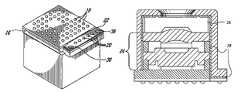
- FIG. 1Shown in FIG. 1 is a fully assembled Wafer Level Camera (WLC) module including an active optical element, according to a non-limiting embodiment of the proposed solution.
- WLCWafer Level Camera
- Such a camera modulecan be intended for integration into a portable telephone, for example, or more specifically for mounting on the main Printed Circuit Board (PCB) of a cellular telephone.
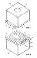
- a camera housing 10 in this embodimentis roughly cubical, although it can take a number of different forms as well.
- the camera housing (or “cover”) 10can be a molded component that prevents light leakage into the camera and protects the camera module.
- the camera housing coveris designed and molded in such a way that it is able to receive and contain all of the various elements of the camera module.
- the camera housing 10is made of a polymer material, such as but not limited to plastic.
- Camera housing 10also includes a flange 12 that, as discussed in more detail below, which is used to cover a portion of an internal flexible circuit board, and includes alignment holes 14 via which the internal components of the camera can be mutually aligned.
- the cover 10 ( 12 )sits on a base substrate 16 , which can be an optical detector package that includes a CMOS image sensor in a Ball Grid Array (BGA) Chip-Scale Package (CSP) suitable for wafer level assembly.
- BGABall Grid Array
- CSPChip-Scale Package
- FIG. 2which is a perspective view of the underside of the assembly illustrated in FIG. 1
- the bottom surface of the base substrate 16has a multitude (plurality) of solder balls 18 via which electrical contact can be made with device components, such as an image sensor.
- Solder balls 20are also located on the underside of a stiffener portion 22 of a flexible circuit board, which is discussed in more detail below.
- the assembly processitself provides for all of the necessary electrical connections to the active optical element of the camera, such as a Tunable Liquid Crystal Lens (TLCL), without requiring any additional steps to make the necessary electrical contact(s).
- Tunable Liquid Crystal LensTunable Liquid Crystal Lens
- the active optical elementcan comprise a tunable lens, shutter, beam steering device, diaphragm, variable filter, etc. as will be apparent to a person skilled in the art.
- the wafer camera moduleis formed of various separate elements, which are assembled together within the molded camera cover ( 10 ).
- these elementsinclude an image CMOS sensor 23 , a wafer level fixed lens structure 24 , an active optical element such as TLCL 26 and a flexible printed circuit 28 providing an electrical circuit conduction path for the active optical element.
- the image CMOS sensoris pre-packaged in Ball Grid Array (BGA) Chip-Scale Package (CSP) 16 suitable for wafer level assembly.
- BGABall Grid Array
- CSPChip-Scale Package
- the CMOS sensor BGA-CSPis characterized by a plurality of solder balls provided on its bottom surface. These solder balls are intended for reflow soldering to a PCB upon mounting of the fully assembled camera module to a device, such as the PCB of a cellular phone, thus making electrical connections between the image sensor ( 23 ) and the device substrate.
- the wafer level fixed lens structure 24includes multiple lens elements suitable for focusing incident light onto the image CMOS sensor 23 .
- This fixed lens structure 24which can be mounted on a glass substrate and can be characterized by various shapes, sizes and thicknesses, acts to focus light from a subject that is collected via the aperture of the camera.
- the wafer level fixed lens structure ( 24 )is characterized by multiple glass layers with replicated surfaces, forming an optical structure similar to conventional lens elements in a camera.
- Light from a subject in front of the fixed lens structure ( 24 )is collected via entrance aperture 30 and is focused by the lens structure ( 24 ) to form an image on a desired imaging device, in this case the CMOS sensor 23 of the WLC.
- the TLCLcan be located at any desired position within the stack of lenses.
- the aperture of the TLCLcan be made smaller when the TLCL is located within the stack at a position where the lens aperture is smaller.
- the active optical element 26 of the module shown in FIG. 3is a tunable lens, providing an auto focus function for the wafer level camera.
- the tunable lensis a Tunable Liquid Crystal Lens (TLCL), such as that discussed in U.S. Provisional Patent Application Ser. No. 61/059,274, filed Jun. 6, 2008, the substance of which is incorporated herein by reference.
- TLCLTunable Liquid Crystal Lens
- a TLCLis a liquid crystal based lens structure for which the focusing power changes with changes to an applied electric field. As the electric field is typically generated by an input electrical signal, variation of that signal can be used to change the tuning of the lens.
- the tuning range of the TLCLmay include a zero optical power level at which it adds no focusing effect to the overall lens structure.
- the electrical signal supplied to the TLCLchanges, the optical power of the liquid crystal lens changes with it, causing an overall change in the focal length of the variable focus lens.
- the TLCL 26is separate from the wafer level fixed lens structure 24 , positioned adjacent the fixed lens structure 24 within the assembled camera module.
- the TLCL 26can also be located at different positions within the assembled camera module, without departing from the scope of the present invention.
- the TLCL 26can be integrated within the fixed lens structure ( 24 ), sandwiched between two of the layers, thus forming a variable focus lens structure.
- the focus plane of the fixed lens structurecan be actively adjusted to compensate for improper distance of the lens stack from the CMOS sensor 23 .
- the TLCL 26can be located at a position in the lens camera module where the light passing through it will be at a relatively narrow focus, that is, where a cross sectional area of the light passing through the TLCL 26 is minimum. In this way, the size of the TLCL 26 and the actively controlled area of the lens can be minimized.
- the TLCLcan be part of a structure that has a TLCL located in a substrate to which is attached one or more fixed lenses.
- a lens structure such as thisis disclosed in International Patent Application PCT/CA2009/001181, the substance of which is incorporated herein by reference.
- Flexible Printed Circuit (FPC) 28is provided within the camera module to create electrical conduction paths (electrical connections) from the active optical element, i.e. the TLCL 26 , to the substrate on which is mounted the camera module, e.g. the PCB of a cellular phone.
- the FPC 28is shaped to receive and contain the TLCL 26 of the camera module, as well at least a portion of the fixed lens structure 24 . More specifically, the FPC 28 has a substantially flat upper surface, bearing an aperture substantially matching the camera aperture 30 , with four walls 32 (tabs) extending downwardly therefrom.
- a particular one of these wallshas a portion 34 that extends into stiffener 22 of the FPC, the height of this particular wall being such that, upon assembly of the WLC module, the stiffener 22 of the FPC is substantially co-planar with the CSP-BGA sensor package 16 .
- the perspective view of FIG. 4which depicts the assembled camera module without cover 10 , illustrates how the FPC 28 fits over the TLCL 26 and fixed lens structure 24 , such that the bottom of stiffener 22 is substantially aligned with the bottom of base substrate 16 .
- the stiffener 22 of the FPC 28includes multiple solder balls 20 provided on the bottom thereof, for reflow soldering of the FPC (PCB) to a host circuit board upon mounting of the camera module thereto.
- the solder balls 20 on the stiffener 22are characterized by a specific spacing, size and shape in order to substantially match that of the solder balls 18 of the sensor BGA. This similarity among all of the solder balls and their spacing can be important to ensure that the fully assembled WLC, including the TLCL, is a BGA-like package.
- FIGS. 5A and 5Brepresent, respectively, a side view and a bottom view of the assembled camera module.
- an FPCbears conductive pathways or traces that serve to make electrical connections.
- the conductive pathways of the FPC 28allow convenient electrical signal routing between the TLCL 26 and the PCB of a cellular phone. More specifically, the FPC is designed such that its conductive pathways or traces are provided thereon according to a layout that ensures electrical connection can be made to one or more contact points of the TLCL, when this TLCL 26 is received within the FPC 28 .
- These conductive pathways or tracesrun down the particular wall of the FPC that ends in the stiffener 22 , thus conducting signals to the active optical element from the conductors (i.e., solder balls 20 ) of the stiffener 22 .
- the FPCcan be mounted and electrically connected to the TLCL 26 by way of conductive film bonding, such as an Anisotropic Conductive Film (ACF) bonding process, or by using conductive adhesive (e.g., conductive sheet adhesives), among many other possibilities.
- conductive film bondingsuch as an Anisotropic Conductive Film (ACF) bonding process
- conductive adhesivee.g., conductive sheet adhesives
- the use of conductive sheet adhesives to mount the FPC to the TLCLallows for the FPC to strain-relieve itself as it conforms to the lens stack of the camera module.
- at least one side of the FPC 28can be given clearance space and left without bonding to the TLCL, thus allowing the FPC to compress or otherwise bend to accommodate variations in lens height tolerance.
- the stiffener 22 of the FPCcan be reflow soldered (to a substrate of the WLC module) for example to a cell phone PCB. Accordingly, the FPC 28 is operative to conduct electrical signals between the variable focus lens structure (i.e., TLCL 26 ) of the WLC module and the PCB, along the vertical wall of the camera module and via the electrical contact points made between the stiffener 22 and the PCB. As shown in FIG. 2 , the stiffener 22 of the FPC 28 is characterized by a pair of alignment holes 36 used to align the FPC to the camera cover 10 , as will be discussed in further detail below. This stiffener 22 can also be used to create a proper structure for attachment of the camera module to the PCB.
- TLCL 26variable focus lens structure
- the cover 10Upon assembly, the cover 10 is aligned with and attached to both the sensor BGA 16 and the FPC 28 , in order to maintain these two elements in proper aligned position within the cover 10 .
- the camera cover (or housing) 10includes a flange 12 at its bottom end, which has alignment holes 14 for providing proper alignment of the elements of the camera module. More specifically, upon assembly of the WLC module, the stiffener 22 of the FPC 28 is received within the flange 12 of the camera cover 10 , and the alignment holes 36 of the stiffener 22 are aligned with the alignment holes 14 of the camera cover flange 12 , thus ensuring proper alignment of the solder balls 20 on the FPC with the solder balls 18 of the CMOS sensor BGA 16 . More specifically, the solder balls 20 of the FPC stiffener 22 are positioned to be physically substantially parallel with the solder balls 18 of the sensor BGA 16 when the camera is fully assembled.
- the WLC modulecan be constructed following different assembly sequences, depending on test and yield requirements of different elements of the camera.
- the elements of the WLC moduleare assembled in the following sequence:
- the fully assembled wafer level camera moduleis illustrated in the external perspective view of FIG. 1 , and is also illustrated in partial cross-section in FIG. 6 .
- the TLCL 26is illustrated to indicate its position relative to the module components (FPC 28 ).
- the moduleis a structured BGA-like package that includes an active optical element, notably the auto-focus TLCL 26 along with a fixed lens structure 24 and FPC 28 .
- this packaging of the WLC with active optical elementallows for the active optical element to be assembled to the PCB of a cellular phone like any other BGA, without the need for additional or special assembly steps to make the necessary electrical connections to the active optical element.
- the packaged WLC module, in its final assembled formis a fully testable component that can be mounted to a PCB using an automatic pick-and-place process and reflow soldering.
- FIG. 7An alternative embodiment of the proposed is shown in FIG. 7 .
- the base substrate 40extends further than the base substrate 16 of FIGS. 1-6 and has solder balls 42 that provide connection points both for the image sensor and the for the active optical element. Electrical contact to the active optical element is made via flexible printed circuit 44 , which makes contact with conductive pads 46 on the top of the substrate 40 that are, in turn, connected to respective solder balls 42 on the bottom surface of the substrate.
- the flexible printed circuit 44is similar to flexible printed circuit 28 of the foregoing embodiments, but does not include stiffener 22 . Rather, the contact portion 48 has electrical contacts that make a connection with the conductive pads 46 of the substrate.
- there is only one continuous contact surface on the base of the (WLC) deviceand there is no need to align two portions at the mounting surface of the camera module.
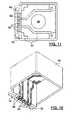
- FIG. 8Shown in FIG. 8 is a fully assembled Wafer Level Camera (WLC) module including an active optical element, according to another non-limiting embodiment of the proposed solution.
- WLCWafer Level Camera
- a WLC modulecan be integrated into a portable telephone or more specifically intended for mounting on a main Printed Circuit Board (PCB) of a cellular telephone.
- a camera housing 50 in this embodimentis roughly cubical, although it can take a number of different shapes as well.
- the camera housing (or “cover”) 50can be a molded component which prevents light leakage into the camera and protects the WLC module.
- the camera housing cover 50is designed and molded in such a way that it is able to receive and contain all of the various elements of the WCL module.
- the camera housing 50is made of a polymer material, such as but not limited to plastic.
- Camera housing 50also includes a flange 52 which includes alignment holes 14 via which the internal components of the camera can be mutually aligned.
- flange 52is used to carry portion of an internal LDS (Laser Direct Structuring) circuit structure used inside the plastic housing.
- the cover 50 ( 52 )sits on a base substrate 16 , which can be an optical detector package which for example includes a CMOS image sensor in a Ball Grid Array (BGA) Chip-Scale Package (CSP) suitable for wafer level assembly.
- BGABall Grid Array
- CSPChip-Scale Package
- FIG. 9which is a perspective view of the underside of the assembly illustrated in FIG. 8
- the bottom surface of the base substrate 16has a multitude (plurality) of solder balls 18 via which electrical contact can be made with device components, such as an image sensor.
- Solder balls 60are also located on the underside of flange portion 52 supporting the LDS circuit structure, which is discussed in more detail below.
- the assembly processitself provides for all of the necessary electrical connections to the active optical element of the camera, such as a Tunable Liquid Crystal Lens (TLCL), without requiring any additional steps to make the necessary electrical contact(s).
- TCLTunable Liquid Crystal Lens
- the active optical elementcan comprise a tunable lens, shutter, beam steering device, diaphragm, variable filter, etc. as will be apparent to a person skilled in the art.
- LDSLaser Direct Structuring
- an injection molded componentsuch as camera housing 50 to be selectively plated with discrete conductive pathways 62 collectively forming an LDS circuit structure.
- the camera housing 50is injection molded using a polymer compound formulated specifically for the LDS process.
- the camera housing 50is then traced with a laser in the pattern of the LDS circuit structure to activate the surface of the camera housing 50 in the areas traced with the laser.
- the camera housing 50then undergoes a plating process, for example with electroless copper, electroless nickel and immersion gold.
- the LDS processprovides an LDS circuit trace structure which follows the contour of the injection molded camera housing 50 in three dimensions.
- manufacturing, stocking, and assembling discrete connecting partssuch as the flexible printed circuit components can be reduced.
- the wafer camera moduleis formed of various separate elements, which are assembled together within the molded camera cover 50 .
- the elementsinclude an image CMOS sensor 23 , a wafer level fixed lens structure 24 , an active optical element such as TLCL 26 and the camera housing 50 having the LDS circuit structure ( 62 ) providing an electrical circuit conduction path for the active optical element.
- the LDS circuit structure ( 62 )is provided within the camera module to create electrical conduction paths (electrical connections) from the active optical element, i.e. the TLCL 26 , to the substrate on which the camera module is mounted, e.g. the PCB of a cellular phone.
- the camera housing 50 with the LDS circuit structure ( 62 )is shaped to receive and contain the TLCL 26 of the camera module, as well (at least a portion of) the fixed lens structure 24 . More specifically, the LDS circuit structure ( 62 ) has conductive pathways 62 along the walls and flange 52 of the camera housing 50 .
- a particular one of these wallsextends into flange 52 , the height of this particular wall being such that, upon assembly of the WLC module, the flange 52 is substantially co-planar with the CSP-BGA sensor package 16 for example as illustrated in FIG. 9 .
- the assembled camera module with cover 50fits over the TLCL 26 and fixed lens structure 24 such that the bottom of flange 52 is substantially aligned with the bottom of base substrate 16 .
- the flange 52includes multiple solder balls 60 provided on the bottom thereof, for reflow soldering of to a host circuit board upon mounting of the camera module thereto.
- the solder balls 60 on the flange 52are characterized by a specific spacing, size and shape in order to substantially match that of the solder balls 18 of the sensor BGA. This similarity among all of the solder balls and their spacing can be important to ensure that the fully assembled WLC, including the TLCL, is a BGA-like package.
- FIGS. 13A and 13Brepresent, respectively, a side view and a bottom view of the assembled camera module.
- the LDS circuit structurebears conductive pathways 62 or traces that serve to make electrical connections.
- the conductive pathways 62 of the LDS circuit structureallow convenient electrical signal routing between the TLCL 26 and the PCB of a cellular phone.
- LDS circuit structure on the camera housing 50is designed such that its conductive pathways 62 or traces are provided thereon according to a layout that ensures electrical connection can be made to one or more contact points of the TLCL, when this TLCL 26 is received within the camera housing 50 .
- These conductive pathways 62 or tracesrun down the particular wall of the camera housing 50 that ends in the flange 52 , thus conducting signals to the active optical element ( 26 ) from the conductors (i.e., solder balls 60 ) of the flange 52 .
- the LDS circuit structurecan be electrically connected to the TLCL 26 by way of conductive film bonding, such as an Anisotropic Conductive Film (ACF) bonding process, or by using conductive adhesive (e.g., conductive sheet adhesives), among many other possibilities.
- conductive film bondingsuch as an Anisotropic Conductive Film (ACF) bonding process
- conductive adhesivee.g., conductive sheet adhesives
- the use of conductive sheet adhesives to mount the camera housing 50 with the LDS circuit structure thereon to the TLCL 26allows for strain-relief between the camera housing 50 the lens stack 24 of the camera module.
- the flange 52 of the camera housing 50can be reflow soldered for example to a cell phone PCB.
- the LDS circuit structureis operative to conduct electrical signals between the variable focus lens structure (i.e., TLCL 26 ) of the WLC module and the PCB, along the vertical wall of the camera module 50 and via the electrical contact points made between the flange 52 and the PCB.
- the flange 52 of the camera housing 50is characterized by a pair of alignment holes 14 used to create a proper structure for attachment of the camera module to the PCB.
- the cover 50Upon assembly, the cover 50 is aligned with and attached to the sensor BGA 16 in order to maintain these two elements in proper aligned position.
- the camera cover (or housing) 50includes a flange 52 at its bottom end, which has alignment holes 14 for providing proper alignment of the elements of the camera module. More specifically, upon assembly of the WLC module, the flange 52 of the camera cover 50 employs the alignment holes 14 to ensure proper alignment of the solder balls 60 on the flange 52 with the solder balls 18 of the CMOS sensor BGA 16 . More specifically, the solder balls 60 of the flange 52 are positioned to be substantially parallel with the solder balls 18 of the sensor BGA 16 when the camera is fully assembled.
- the WLC modulecan be constructed following different assembly sequences, depending on test and yield requirements of different elements of the camera.
- the elements of the WLC moduleare assembled in the following sequence:
- the fully assembled wafer level camera moduleis illustrated in the external perspective view of FIG. 8 , and is also illustrated in partial cross-section in FIG. 14 .
- the TLCL 26is illustrated to indicate its position relative to the module components.
- the moduleis a structured BGA-like package that includes an active optical element, notably the auto-focus TLCL 26 along with a fixed lens structure 24 .
- this packaging of the WLC with active optical elementallows for the active optical element to be assembled to the PCB of a cellular phone like any other BGA, without the need for additional or special assembly steps to make the necessary electrical connections to the active optical element.
- the packaged WLC module, in its final assembled form,is a fully testable component that can be mounted to a PCB using an automatic pick-and-place process and reflow soldering.
- control circuitry(not shown) connected to the TLCL.
- control circuitrynot shown
- PCT publication WO/2010/022080published on 25 Feb. 2010, which is incorporated herein by reference.
- the inventionis not limited to active optical elements, such as TLCL 26 , having top surface electrical contact structures, and can apply equally well active optical elements having an edge connect structure as described in International Patent Application PCT/CA2009/000742 filed Jun. 5, 2009, which is incorporated herein by reference.
- the wafer level camera modulecan include additional elements, with varying functionality, without departing from the scope of the present invention.
Landscapes
- Engineering & Computer Science (AREA)
- Multimedia (AREA)
- Signal Processing (AREA)
- Transforming Light Signals Into Electric Signals (AREA)
- Studio Devices (AREA)
- Lens Barrels (AREA)
- Structures For Mounting Electric Components On Printed Circuit Boards (AREA)
- Solid State Image Pick-Up Elements (AREA)
Abstract
Description
- 1. Attach the TLCL to the wafer level fixed lens structure in wafer form.
- 2. Assemble this variable focus lens structure to a CSP packaged wafer of CMOS sensors.
- 3. Dice and separate the modules to form individual wafer level camera modules.
- 4. Attach the FPC to a WLC module using an anisotropic conductive film (ACF) bonding process or a conductive adhesive.
- 5. Attach the camera cover to the CSP package and FPC, using the alignment holes to create proper alignment of solder balls on the FPC to the camera cover and in turn to the solder balls on the BGA-CSP.
- 1. Attach the TLCL to the wafer level fixed lens structure in wafer form.
- 2. Assemble this variable focus lens structure to a CSP packaged wafer of CMOS sensors.
- 3. Dice and separate the modules to form individual wafer level camera modules.
- 4. Attach the camera cover to the CSP package using an anisotropic conductive film (ACF) bonding process or a conductive adhesive and using the alignment holes to create proper alignment between solder balls on the
flange 52 and the solder balls on the BGA-CSP.
Claims (27)
Priority Applications (1)
| Application Number | Priority Date | Filing Date | Title |
|---|---|---|---|
| US13/338,756US8891006B2 (en) | 2009-06-29 | 2011-12-28 | Wafer level camera module with active optical element |
Applications Claiming Priority (3)
| Application Number | Priority Date | Filing Date | Title |
|---|---|---|---|
| US22140809P | 2009-06-29 | 2009-06-29 | |
| PCT/US2010/039595WO2011008443A2 (en) | 2009-06-29 | 2010-06-23 | Wafer level camera module with active optical element |
| US13/338,756US8891006B2 (en) | 2009-06-29 | 2011-12-28 | Wafer level camera module with active optical element |
Related Parent Applications (1)
| Application Number | Title | Priority Date | Filing Date |
|---|---|---|---|
| PCT/US2010/039595Continuation-In-PartWO2011008443A2 (en) | 2009-06-29 | 2010-06-23 | Wafer level camera module with active optical element |
Publications (2)
| Publication Number | Publication Date |
|---|---|
| US20120140101A1 US20120140101A1 (en) | 2012-06-07 |
| US8891006B2true US8891006B2 (en) | 2014-11-18 |
Family
ID=43450061
Family Applications (1)
| Application Number | Title | Priority Date | Filing Date |
|---|---|---|---|
| US13/338,756Active2031-02-20US8891006B2 (en) | 2009-06-29 | 2011-12-28 | Wafer level camera module with active optical element |
Country Status (2)
| Country | Link |
|---|---|
| US (1) | US8891006B2 (en) |
| WO (1) | WO2011008443A2 (en) |
Cited By (3)
| Publication number | Priority date | Publication date | Assignee | Title |
|---|---|---|---|---|
| US20150145966A1 (en)* | 2013-11-27 | 2015-05-28 | Children's National Medical Center | 3d corrected imaging |
| US20150230348A1 (en)* | 2014-02-13 | 2015-08-13 | Samsung Electronics Co., Ltd. | Electronic device including opening |
| US20210048562A1 (en)* | 2018-01-23 | 2021-02-18 | Lg Innotek Co., Ltd. | Liquid lens module, lens assembly including the same, and camera module including the lens assembly |
Families Citing this family (96)
| Publication number | Priority date | Publication date | Assignee | Title |
|---|---|---|---|---|
| US7825985B2 (en) | 2007-07-19 | 2010-11-02 | Flextronics Ap, Llc | Camera module back-focal length adjustment method and ultra compact components packaging |
| US11792538B2 (en) | 2008-05-20 | 2023-10-17 | Adeia Imaging Llc | Capturing and processing of images including occlusions focused on an image sensor by a lens stack array |
| DK3876510T3 (en) | 2008-05-20 | 2024-11-11 | Adeia Imaging Llc | CAPTURE AND PROCESSING OF IMAGES USING MONOLITHIC CAMERA ARRAY WITH HETEROGENEOUS IMAGES |
| US8866920B2 (en) | 2008-05-20 | 2014-10-21 | Pelican Imaging Corporation | Capturing and processing of images using monolithic camera array with heterogeneous imagers |
| EP2502115A4 (en) | 2009-11-20 | 2013-11-06 | Pelican Imaging Corp | CAPTURE AND IMAGE PROCESSING USING A MONOLITHIC CAMERAS NETWORK EQUIPPED WITH HETEROGENEOUS IMAGERS |
| KR20110064156A (en)* | 2009-12-07 | 2011-06-15 | 삼성전자주식회사 | Imaging Device and Manufacturing Method Thereof |
| CN102238319A (en)* | 2010-04-26 | 2011-11-09 | 鸿富锦精密工业(深圳)有限公司 | Image pickup device |
| US8928793B2 (en) | 2010-05-12 | 2015-01-06 | Pelican Imaging Corporation | Imager array interfaces |
| TWI484243B (en)* | 2010-06-10 | 2015-05-11 | Hon Hai Prec Ind Co Ltd | Lens module and camera device |
| US8878950B2 (en) | 2010-12-14 | 2014-11-04 | Pelican Imaging Corporation | Systems and methods for synthesizing high resolution images using super-resolution processes |
| US8559806B2 (en)* | 2010-12-29 | 2013-10-15 | Samsung Electro-Mechanics Co., Ltd. | Camera module and method for manufacturing the same |
| WO2012116302A2 (en)* | 2011-02-24 | 2012-08-30 | Flextronics Ap, Llc | Autofocus-zoom camera module integrating liquid crystal device as high speed shutter |
| WO2012161802A2 (en)* | 2011-02-24 | 2012-11-29 | Flextronics Ap, Llc | Autofocus camera module packaging with circuitry-integrated actuator system |
| US8545114B2 (en) | 2011-03-11 | 2013-10-01 | Digitaloptics Corporation | Auto focus-zoom actuator or camera module contamination reduction feature with integrated protective membrane |
| EP2708019B1 (en) | 2011-05-11 | 2019-10-16 | FotoNation Limited | Systems and methods for transmitting and receiving array camera image data |
| KR101944280B1 (en) | 2011-05-18 | 2019-01-31 | 엘지이노텍 주식회사 | Camera Module |
| US8896743B2 (en)* | 2011-06-08 | 2014-11-25 | Omnivision Technologies, Inc. | Enclosure for image capture systems with focusing capabilities |
| US8878976B2 (en)* | 2011-06-08 | 2014-11-04 | Omnivision Technologies, Inc. | Image capture systems with focusing capabilities |
| US20130265459A1 (en) | 2011-06-28 | 2013-10-10 | Pelican Imaging Corporation | Optical arrangements for use with an array camera |
| US20130070060A1 (en) | 2011-09-19 | 2013-03-21 | Pelican Imaging Corporation | Systems and methods for determining depth from multiple views of a scene that include aliasing using hypothesized fusion |
| CN104081414B (en) | 2011-09-28 | 2017-08-01 | Fotonation开曼有限公司 | Systems and methods for encoding and decoding light field image files |
| WO2013055960A1 (en)* | 2011-10-11 | 2013-04-18 | Pelican Imaging Corporation | Lens stack arrays including adaptive optical elements |
| EP2817955B1 (en) | 2012-02-21 | 2018-04-11 | FotoNation Cayman Limited | Systems and methods for the manipulation of captured light field image data |
| US9210392B2 (en) | 2012-05-01 | 2015-12-08 | Pelican Imaging Coporation | Camera modules patterned with pi filter groups |
| KR101940478B1 (en)* | 2012-05-07 | 2019-01-21 | 엘지이노텍 주식회사 | Camera Module |
| KR102033171B1 (en)* | 2012-06-22 | 2019-10-16 | 엘지이노텍 주식회사 | Camera Module |
| JP2015534734A (en) | 2012-06-28 | 2015-12-03 | ペリカン イメージング コーポレイション | System and method for detecting defective camera arrays, optical arrays, and sensors |
| US20140002674A1 (en) | 2012-06-30 | 2014-01-02 | Pelican Imaging Corporation | Systems and Methods for Manufacturing Camera Modules Using Active Alignment of Lens Stack Arrays and Sensors |
| KR102107654B1 (en)* | 2012-07-30 | 2020-05-07 | 엘지이노텍 주식회사 | Camera Module |
| TW201408060A (en)* | 2012-08-06 | 2014-02-16 | Hon Hai Prec Ind Co Ltd | Camera module and method for making camera module |
| CN107889344A (en)* | 2012-08-15 | 2018-04-06 | 深圳迈辽技术转移中心有限公司 | Flexible printed circuit device |
| PL4296963T3 (en) | 2012-08-21 | 2025-04-28 | Adeia Imaging Llc | Method for depth detection in images captured using array cameras |
| WO2014032020A2 (en) | 2012-08-23 | 2014-02-27 | Pelican Imaging Corporation | Feature based high resolution motion estimation from low resolution images captured using an array source |
| US9214013B2 (en) | 2012-09-14 | 2015-12-15 | Pelican Imaging Corporation | Systems and methods for correcting user identified artifacts in light field images |
| CN202773174U (en)* | 2012-09-14 | 2013-03-06 | 豪威科技(上海)有限公司 | Reinforcement structure for protecting wafer level camera module |
| CN103715208B (en)* | 2012-09-28 | 2016-12-21 | 意法半导体研发(深圳)有限公司 | There is bonding and fill image device and the correlation technique of opening |
| EP4307659A1 (en) | 2012-09-28 | 2024-01-17 | Adeia Imaging LLC | Generating images from light fields utilizing virtual viewpoints |
| WO2014078443A1 (en) | 2012-11-13 | 2014-05-22 | Pelican Imaging Corporation | Systems and methods for array camera focal plane control |
| CN103813070A (en)* | 2012-11-14 | 2014-05-21 | 鸿富锦精密工业(深圳)有限公司 | Imaging device |
| US9462164B2 (en) | 2013-02-21 | 2016-10-04 | Pelican Imaging Corporation | Systems and methods for generating compressed light field representation data using captured light fields, array geometry, and parallax information |
| US9374512B2 (en) | 2013-02-24 | 2016-06-21 | Pelican Imaging Corporation | Thin form factor computational array cameras and modular array cameras |
| US9774789B2 (en) | 2013-03-08 | 2017-09-26 | Fotonation Cayman Limited | Systems and methods for high dynamic range imaging using array cameras |
| US8866912B2 (en) | 2013-03-10 | 2014-10-21 | Pelican Imaging Corporation | System and methods for calibration of an array camera using a single captured image |
| WO2014165244A1 (en) | 2013-03-13 | 2014-10-09 | Pelican Imaging Corporation | Systems and methods for synthesizing images from image data captured by an array camera using restricted depth of field depth maps in which depth estimation precision varies |
| US9124831B2 (en) | 2013-03-13 | 2015-09-01 | Pelican Imaging Corporation | System and methods for calibration of an array camera |
| US9106784B2 (en) | 2013-03-13 | 2015-08-11 | Pelican Imaging Corporation | Systems and methods for controlling aliasing in images captured by an array camera for use in super-resolution processing |
| US9888194B2 (en) | 2013-03-13 | 2018-02-06 | Fotonation Cayman Limited | Array camera architecture implementing quantum film image sensors |
| US9578259B2 (en) | 2013-03-14 | 2017-02-21 | Fotonation Cayman Limited | Systems and methods for reducing motion blur in images or video in ultra low light with array cameras |
| WO2014153098A1 (en) | 2013-03-14 | 2014-09-25 | Pelican Imaging Corporation | Photmetric normalization in array cameras |
| US9438888B2 (en) | 2013-03-15 | 2016-09-06 | Pelican Imaging Corporation | Systems and methods for stereo imaging with camera arrays |
| US9445003B1 (en) | 2013-03-15 | 2016-09-13 | Pelican Imaging Corporation | Systems and methods for synthesizing high resolution images using image deconvolution based on motion and depth information |
| US9497429B2 (en) | 2013-03-15 | 2016-11-15 | Pelican Imaging Corporation | Extended color processing on pelican array cameras |
| WO2014150856A1 (en) | 2013-03-15 | 2014-09-25 | Pelican Imaging Corporation | Array camera implementing quantum dot color filters |
| US10122993B2 (en) | 2013-03-15 | 2018-11-06 | Fotonation Limited | Autofocus system for a conventional camera that uses depth information from an array camera |
| CN104253133B (en)* | 2013-06-26 | 2017-07-28 | 深圳赛意法微电子有限公司 | Camera module and preparation method thereof |
| CN104469099A (en)* | 2013-09-25 | 2015-03-25 | 深圳富泰宏精密工业有限公司 | Camera installation structure and portable electronic device comprising same |
| US9898856B2 (en) | 2013-09-27 | 2018-02-20 | Fotonation Cayman Limited | Systems and methods for depth-assisted perspective distortion correction |
| US9671671B2 (en)* | 2013-10-10 | 2017-06-06 | Stmicroelectronics Pte Ltd | Optical assembly including electrically conductive coupling member and related methods |
| US9264592B2 (en) | 2013-11-07 | 2016-02-16 | Pelican Imaging Corporation | Array camera modules incorporating independently aligned lens stacks |
| US10119808B2 (en) | 2013-11-18 | 2018-11-06 | Fotonation Limited | Systems and methods for estimating depth from projected texture using camera arrays |
| WO2015081279A1 (en) | 2013-11-26 | 2015-06-04 | Pelican Imaging Corporation | Array camera configurations incorporating multiple constituent array cameras |
| US10089740B2 (en) | 2014-03-07 | 2018-10-02 | Fotonation Limited | System and methods for depth regularization and semiautomatic interactive matting using RGB-D images |
| KR102217098B1 (en)* | 2014-04-17 | 2021-02-18 | 엘지이노텍 주식회사 | Camera module |
| US9521319B2 (en) | 2014-06-18 | 2016-12-13 | Pelican Imaging Corporation | Array cameras and array camera modules including spectral filters disposed outside of a constituent image sensor |
| JP2017531976A (en) | 2014-09-29 | 2017-10-26 | フォトネイション ケイマン リミテッド | System and method for dynamically calibrating an array camera |
| US9768216B2 (en)* | 2014-11-07 | 2017-09-19 | Stmicroelectronics Pte Ltd | Image sensor device with different width cell layers and related methods |
| US9942474B2 (en) | 2015-04-17 | 2018-04-10 | Fotonation Cayman Limited | Systems and methods for performing high speed video capture and depth estimation using array cameras |
| US9703173B2 (en)* | 2015-04-21 | 2017-07-11 | Apple Inc. | Camera module structure having electronic device connections formed therein |
| US10426037B2 (en) | 2015-07-15 | 2019-09-24 | International Business Machines Corporation | Circuitized structure with 3-dimensional configuration |
| US10021280B2 (en)* | 2015-08-18 | 2018-07-10 | Apple Inc. | Camera module electrical architecture |
| US10261001B2 (en)* | 2015-10-21 | 2019-04-16 | Flir Detection, Inc. | Manually operated desorber for sensor detector device |
| EP3369359A4 (en)* | 2015-10-27 | 2019-06-05 | Olympus Corporation | Imaging device and endoscope |
| US10026765B2 (en)* | 2015-11-11 | 2018-07-17 | Pixart Imaging (Penang) Sdn. Bhd. | Apparatus and sensor chip component attaching method |
| US9933601B2 (en)* | 2015-12-16 | 2018-04-03 | Intel Corporation | Stacked wafer lens and camera |
| WO2017180060A1 (en) | 2016-04-15 | 2017-10-19 | Heptagon Micro Optics Pte. Ltd. | Optoelectronic modules with alignment spacers and methods for assembling the same |
| US11150438B2 (en) | 2016-08-10 | 2021-10-19 | Apple Inc. | Protected interconnect for solid state camera module |
| US10482618B2 (en) | 2017-08-21 | 2019-11-19 | Fotonation Limited | Systems and methods for hybrid depth regularization |
| US10750061B2 (en)* | 2017-09-15 | 2020-08-18 | Omnivision Technologies, Inc. | Endoscope having camera module and LED on flexible printed circuit |
| US11270110B2 (en) | 2019-09-17 | 2022-03-08 | Boston Polarimetrics, Inc. | Systems and methods for surface modeling using polarization cues |
| WO2021071992A1 (en) | 2019-10-07 | 2021-04-15 | Boston Polarimetrics, Inc. | Systems and methods for augmentation of sensor systems and imaging systems with polarization |
| DE112020005932T5 (en) | 2019-11-30 | 2023-01-05 | Boston Polarimetrics, Inc. | SYSTEMS AND METHODS FOR SEGMENTATION OF TRANSPARENT OBJECTS USING POLARIZATION CHARACTERISTICS |
| EP4081933A4 (en) | 2020-01-29 | 2024-03-20 | Intrinsic Innovation LLC | Systems and methods for characterizing object pose detection and measurement systems |
| US11797863B2 (en) | 2020-01-30 | 2023-10-24 | Intrinsic Innovation Llc | Systems and methods for synthesizing data for training statistical models on different imaging modalities including polarized images |
| US11953700B2 (en) | 2020-05-27 | 2024-04-09 | Intrinsic Innovation Llc | Multi-aperture polarization optical systems using beam splitters |
| US12069227B2 (en) | 2021-03-10 | 2024-08-20 | Intrinsic Innovation Llc | Multi-modal and multi-spectral stereo camera arrays |
| US12020455B2 (en) | 2021-03-10 | 2024-06-25 | Intrinsic Innovation Llc | Systems and methods for high dynamic range image reconstruction |
| US11954886B2 (en) | 2021-04-15 | 2024-04-09 | Intrinsic Innovation Llc | Systems and methods for six-degree of freedom pose estimation of deformable objects |
| US11290658B1 (en) | 2021-04-15 | 2022-03-29 | Boston Polarimetrics, Inc. | Systems and methods for camera exposure control |
| US12067746B2 (en) | 2021-05-07 | 2024-08-20 | Intrinsic Innovation Llc | Systems and methods for using computer vision to pick up small objects |
| US12175741B2 (en) | 2021-06-22 | 2024-12-24 | Intrinsic Innovation Llc | Systems and methods for a vision guided end effector |
| US12340538B2 (en) | 2021-06-25 | 2025-06-24 | Intrinsic Innovation Llc | Systems and methods for generating and using visual datasets for training computer vision models |
| US12172310B2 (en) | 2021-06-29 | 2024-12-24 | Intrinsic Innovation Llc | Systems and methods for picking objects using 3-D geometry and segmentation |
| US11689813B2 (en) | 2021-07-01 | 2023-06-27 | Intrinsic Innovation Llc | Systems and methods for high dynamic range imaging using crossed polarizers |
| US12293535B2 (en) | 2021-08-03 | 2025-05-06 | Intrinsic Innovation Llc | Systems and methods for training pose estimators in computer vision |
| WO2023017598A1 (en)* | 2021-08-12 | 2023-02-16 | オリンパスメディカルシステムズ株式会社 | Imaging unit and endoscope applying said imaging unit |
| US12034200B1 (en)* | 2022-04-20 | 2024-07-09 | Meta Platforms Technologies, Llc | Integrated camera antenna |
Citations (64)
| Publication number | Priority date | Publication date | Assignee | Title |
|---|---|---|---|---|
| US4781445A (en) | 1984-02-23 | 1988-11-01 | Canon Kabushiki Kaisha | Optical device having positionally changeable optical surfaces and a method of varying an image forming position |
| US5592314A (en) | 1993-12-02 | 1997-01-07 | Yazaki Corporation | Tunable wavelength filter formed by 2 lcds in series having opposite twist angles of n*π/2 and a dielectric mirror layer on each substrate |
| US5808679A (en) | 1996-09-06 | 1998-09-15 | Microtek International Inc. | Camera lens assembly using rotatable conductive plate connectors |
| US6359674B1 (en) | 1999-06-08 | 2002-03-19 | Olympus Optical Co., Ltd. | Liquid crystal lens, liquid crystal lens unit, and liquid crystal lens assembly |
| US20020033911A1 (en) | 2000-08-28 | 2002-03-21 | Nobuhisa Ishida | Liquid crystal display apparatus and manufacturing method therefor |
| US20040184163A1 (en) | 2003-02-13 | 2004-09-23 | Olympus Corporation | Optical apparatus |
| JP2005084387A (en) | 2003-09-09 | 2005-03-31 | Konica Minolta Opto Inc | Photography lens and imaging device |
| WO2005098479A1 (en) | 2004-03-31 | 2005-10-20 | Binit Corporation | Double liquid-crystal aberration correcting element and its manufacturing method |
| US20060103758A1 (en) | 2004-11-12 | 2006-05-18 | Samsung Techwin Co., Ltd. | Camera module and method of manufacturing the same |
| US20060203875A1 (en) | 2003-09-26 | 2006-09-14 | Henryk Frenzel | Optical module comprising an image sensor and a lens unit that is supported on the sensitive surface of the image sensor |
| JP2006243573A (en) | 2005-03-07 | 2006-09-14 | Citizen Watch Co Ltd | LCD lens and camera module |
| WO2006106953A1 (en)* | 2005-04-01 | 2006-10-12 | Matsushita Electric Industrial Co., Ltd. | Image pickup device |
| JP2006309011A (en)* | 2005-04-28 | 2006-11-09 | Citizen Watch Co Ltd | Imaging lens and camera module |
| US20070031137A1 (en) | 2003-09-26 | 2007-02-08 | Siemens Ag | Optical module comprising a spacer element between the housing of a semiconductor element and a lens unit |
| US20070063048A1 (en) | 2005-09-14 | 2007-03-22 | Havens William H | Data reader apparatus having an adaptive lens |
| JP2007208587A (en)* | 2006-02-01 | 2007-08-16 | Citizen Electronics Co Ltd | Imaging structure of camera |
| WO2007098602A1 (en) | 2006-03-03 | 2007-09-07 | UNIVERSITé LAVAL | Method and apparatus for spatially modulated electric field generation and electro-optical tuning using liquid crystals |
| US20070242173A1 (en) | 2004-11-02 | 2007-10-18 | Blum Ronald D | Electro-active spectacles and method of fabricating same |
| US7340161B2 (en)* | 2004-11-05 | 2008-03-04 | Smk Corporation | Structure of a camera module with auto-focus feature and a mobile connector therefore |
| WO2008041469A1 (en) | 2006-10-03 | 2008-04-10 | Panasonic Corporation | Imaging device |
| US20080088756A1 (en) | 2006-09-05 | 2008-04-17 | Ling-Yuan Tseng | Tunable liquid crystal lens module |
| US7369327B1 (en) | 1998-06-09 | 2008-05-06 | Olympus Corporation | Variable optical-property element and optical apparatus including the same |
| US20080144186A1 (en) | 2006-12-15 | 2008-06-19 | Chen Feng | Focus module and components with actuator polymer control |
| US20080165427A1 (en) | 2007-01-09 | 2008-07-10 | Cheng-Te Tseng | Image capturing device |
| KR100856092B1 (en)* | 2007-06-18 | 2008-09-02 | 삼성전기주식회사 | Optical lens and camera module with optical lens |
| US20080251707A1 (en) | 2001-10-23 | 2008-10-16 | Tessera North America | Optical chassis, camera having an optical chassis, and associated methods |
| US20080277480A1 (en) | 2007-05-10 | 2008-11-13 | Serge Thuries | Temperature compensated auto focus control for a microfluidic lens, such as auto focus control for a microfluidic lens of a bar code scanner |
| US20080297911A1 (en) | 2007-01-30 | 2008-12-04 | Dmetrix, Inc. | Liquid-lens variable-control optics in array microscope |
| US7469100B2 (en) | 2005-10-03 | 2008-12-23 | Flextronics Ap Llc | Micro camera module with discrete manual focal positions |
| US20090134483A1 (en) | 2007-11-23 | 2009-05-28 | Jui-Ping Weng | Electronic assembly for image sensor device |
| US20090190232A1 (en) | 2008-01-29 | 2009-07-30 | Varioptic S.A. | Optical lens arrangement for fixed lenses and a liquid lens |
| US7614807B2 (en)* | 2006-04-07 | 2009-11-10 | Altus Technology Inc. | Electronic camera mechanism |
| US7619684B2 (en)* | 2003-12-11 | 2009-11-17 | Sharp Kabushiki Kaisha | Camera module, manufacturing method of camera module, electronic apparatus, and manufacturing method of electronic apparatus |
| US20090302116A1 (en) | 2008-06-04 | 2009-12-10 | Symbol Technologies, Inc. | Semi-zoom imaging optical system |
| WO2009153764A2 (en) | 2008-06-21 | 2009-12-23 | Lensvector Inc. | Electro-optical devices using dynamic reconfiguration of effective electrode structures |
| US20090322929A1 (en)* | 2008-06-30 | 2009-12-31 | Hon Hai Precision Industry Co., Ltd. | Compact camera module |
| US7672060B2 (en)* | 2006-08-15 | 2010-03-02 | Stmicroelectronics (Research & Development) Limited | Lens unit |
| WO2010022503A1 (en) | 2008-09-01 | 2010-03-04 | Lensvector Inc. | Wafer-level fabrication of liquid crystal optoelectronic devices |
| US7715107B2 (en) | 2006-04-25 | 2010-05-11 | Asml Netherlands B.V. | Optical element for correction of aberration, and a lithographic apparatus comprising same |
| WO2010083211A1 (en) | 2009-01-15 | 2010-07-22 | E-Vision, Llc | Electro-active focus and zoom systems |
| US20100247086A1 (en)* | 2007-05-14 | 2010-09-30 | Varioptic S.A. | Housing for variable lens |
| US20100276492A1 (en) | 2009-04-29 | 2010-11-04 | Hand Held Products, Inc. | Focusing apparatus and terminal comprising variable focus lens assembly |
| WO2010129454A1 (en)* | 2009-05-03 | 2010-11-11 | Lensvector, Inc. | Optical lens having fixed lenses and embedded active optics |
| US20100295987A1 (en) | 2007-12-13 | 2010-11-25 | Varioptic, S.A. | Image stabilization circuitry for liquid lens |
| US20110134303A1 (en)* | 2009-12-07 | 2011-06-09 | Samsung Electronics Co., Ltd. | Image pickup device and manufacturing method thereof |
| US7959291B2 (en) | 2008-02-21 | 2011-06-14 | Mitutoyo Corporation | Telecentric lens system and vision measuring instrument |
| US20110221950A1 (en)* | 2010-03-12 | 2011-09-15 | Doeke Jolt Oostra | Camera device, wafer scale package |
| US20110261253A1 (en)* | 2010-04-26 | 2011-10-27 | Hon Hai Precision Industry Co., Ltd. | Camera module |
| US20120019761A1 (en) | 2008-06-06 | 2012-01-26 | Lensvector, Inc. | Contact structure for a tunable liquid crystal optical device |
| US20120026451A1 (en)* | 2010-07-29 | 2012-02-02 | Lensvector Inc. | Tunable liquid crystal lens with single sided contacts |
| US8115856B2 (en)* | 2008-03-25 | 2012-02-14 | Hon Hai Precision Industry Co., Ltd. | Camera module |
| US8248523B2 (en)* | 2009-11-05 | 2012-08-21 | Flextronics Ap, Llc | Camera module with fold over flexible circuit and cavity substrate |
| US20120236248A1 (en)* | 2011-03-17 | 2012-09-20 | Samsung Electro-Mechanics Co., Ltd. | Camera module |
| US20120315953A1 (en)* | 2011-06-08 | 2012-12-13 | Zheng Du | Enclosure for image capture systems with focusing capabilities |
| US20130057757A1 (en)* | 2010-05-20 | 2013-03-07 | Lg Innotek Co., Ltd. | Camera module having mems actuator, connecting method for shutter coil of camera module and camera module manufactured by the same method |
| US8411193B2 (en)* | 2010-06-10 | 2013-04-02 | Hon Hai Precision Industry Co., Ltd. | Lens module having liquid crystal lens and image pick-up device using same |
| US8479387B2 (en)* | 2010-05-14 | 2013-07-09 | Kuang Hong Precision Co., Ltd. | Method of manufacturing three-dimensional circuit device |
| US8559806B2 (en)* | 2010-12-29 | 2013-10-15 | Samsung Electro-Mechanics Co., Ltd. | Camera module and method for manufacturing the same |
| US8564718B2 (en)* | 2007-08-21 | 2013-10-22 | Shinko Electric Industries Co., Ltd. | Camera module and mobile terminal unit |
| US20140002727A1 (en)* | 2012-06-29 | 2014-01-02 | Lg Innotek Co., Ltd. | Camera module |
| US20140029120A1 (en)* | 2012-07-30 | 2014-01-30 | Lg Innotek Co., Ltd. | Camera module |
| US20140028905A1 (en)* | 2012-07-30 | 2014-01-30 | Lg Innotek Co., Ltd. | Camera module |
| US20140092296A1 (en)* | 2011-05-18 | 2014-04-03 | Lg Innotek Co., Ltd. | Camera module |
| US8743263B2 (en)* | 2008-12-30 | 2014-06-03 | Datalogic Scanning Group S.R.L. | Liquid lens image capture device |
Family Cites Families (1)
| Publication number | Priority date | Publication date | Assignee | Title |
|---|---|---|---|---|
| JP2006030051A (en)* | 2004-07-20 | 2006-02-02 | Sony Corp | Navigation system, position information registering method, and program |
- 2010
- 2010-06-23WOPCT/US2010/039595patent/WO2011008443A2/enactiveApplication Filing
- 2011
- 2011-12-28USUS13/338,756patent/US8891006B2/enactiveActive
Patent Citations (67)
| Publication number | Priority date | Publication date | Assignee | Title |
|---|---|---|---|---|
| US4781445A (en) | 1984-02-23 | 1988-11-01 | Canon Kabushiki Kaisha | Optical device having positionally changeable optical surfaces and a method of varying an image forming position |
| US5592314A (en) | 1993-12-02 | 1997-01-07 | Yazaki Corporation | Tunable wavelength filter formed by 2 lcds in series having opposite twist angles of n*π/2 and a dielectric mirror layer on each substrate |
| US5808679A (en) | 1996-09-06 | 1998-09-15 | Microtek International Inc. | Camera lens assembly using rotatable conductive plate connectors |
| US7369327B1 (en) | 1998-06-09 | 2008-05-06 | Olympus Corporation | Variable optical-property element and optical apparatus including the same |
| US6359674B1 (en) | 1999-06-08 | 2002-03-19 | Olympus Optical Co., Ltd. | Liquid crystal lens, liquid crystal lens unit, and liquid crystal lens assembly |
| US20020033911A1 (en) | 2000-08-28 | 2002-03-21 | Nobuhisa Ishida | Liquid crystal display apparatus and manufacturing method therefor |
| US20080251707A1 (en) | 2001-10-23 | 2008-10-16 | Tessera North America | Optical chassis, camera having an optical chassis, and associated methods |
| US20040184163A1 (en) | 2003-02-13 | 2004-09-23 | Olympus Corporation | Optical apparatus |
| JP2005084387A (en) | 2003-09-09 | 2005-03-31 | Konica Minolta Opto Inc | Photography lens and imaging device |
| US20060203875A1 (en) | 2003-09-26 | 2006-09-14 | Henryk Frenzel | Optical module comprising an image sensor and a lens unit that is supported on the sensitive surface of the image sensor |
| US20070031137A1 (en) | 2003-09-26 | 2007-02-08 | Siemens Ag | Optical module comprising a spacer element between the housing of a semiconductor element and a lens unit |
| US7619684B2 (en)* | 2003-12-11 | 2009-11-17 | Sharp Kabushiki Kaisha | Camera module, manufacturing method of camera module, electronic apparatus, and manufacturing method of electronic apparatus |
| WO2005098479A1 (en) | 2004-03-31 | 2005-10-20 | Binit Corporation | Double liquid-crystal aberration correcting element and its manufacturing method |
| US20070242173A1 (en) | 2004-11-02 | 2007-10-18 | Blum Ronald D | Electro-active spectacles and method of fabricating same |
| US7340161B2 (en)* | 2004-11-05 | 2008-03-04 | Smk Corporation | Structure of a camera module with auto-focus feature and a mobile connector therefore |
| US20060103758A1 (en) | 2004-11-12 | 2006-05-18 | Samsung Techwin Co., Ltd. | Camera module and method of manufacturing the same |
| JP2006243573A (en) | 2005-03-07 | 2006-09-14 | Citizen Watch Co Ltd | LCD lens and camera module |
| WO2006106953A1 (en)* | 2005-04-01 | 2006-10-12 | Matsushita Electric Industrial Co., Ltd. | Image pickup device |
| US20090213232A1 (en)* | 2005-04-01 | 2009-08-27 | Matsushita Electric Industrial Co., Ltd. | Image pickup device |
| JP2006309011A (en)* | 2005-04-28 | 2006-11-09 | Citizen Watch Co Ltd | Imaging lens and camera module |
| US20070063048A1 (en) | 2005-09-14 | 2007-03-22 | Havens William H | Data reader apparatus having an adaptive lens |
| US7469100B2 (en) | 2005-10-03 | 2008-12-23 | Flextronics Ap Llc | Micro camera module with discrete manual focal positions |
| JP2007208587A (en)* | 2006-02-01 | 2007-08-16 | Citizen Electronics Co Ltd | Imaging structure of camera |
| WO2007098602A1 (en) | 2006-03-03 | 2007-09-07 | UNIVERSITé LAVAL | Method and apparatus for spatially modulated electric field generation and electro-optical tuning using liquid crystals |
| US20070229754A1 (en) | 2006-03-03 | 2007-10-04 | Universite Laval | Method and apparatus for spatially modulated electric field generation and electro-optical tuning using liquid crystals |
| US7614807B2 (en)* | 2006-04-07 | 2009-11-10 | Altus Technology Inc. | Electronic camera mechanism |
| US7715107B2 (en) | 2006-04-25 | 2010-05-11 | Asml Netherlands B.V. | Optical element for correction of aberration, and a lithographic apparatus comprising same |
| US7672060B2 (en)* | 2006-08-15 | 2010-03-02 | Stmicroelectronics (Research & Development) Limited | Lens unit |
| US20080088756A1 (en) | 2006-09-05 | 2008-04-17 | Ling-Yuan Tseng | Tunable liquid crystal lens module |
| WO2008041469A1 (en) | 2006-10-03 | 2008-04-10 | Panasonic Corporation | Imaging device |
| US20080144186A1 (en) | 2006-12-15 | 2008-06-19 | Chen Feng | Focus module and components with actuator polymer control |
| US20080165427A1 (en) | 2007-01-09 | 2008-07-10 | Cheng-Te Tseng | Image capturing device |
| US20080297911A1 (en) | 2007-01-30 | 2008-12-04 | Dmetrix, Inc. | Liquid-lens variable-control optics in array microscope |
| US20080277480A1 (en) | 2007-05-10 | 2008-11-13 | Serge Thuries | Temperature compensated auto focus control for a microfluidic lens, such as auto focus control for a microfluidic lens of a bar code scanner |
| US20100247086A1 (en)* | 2007-05-14 | 2010-09-30 | Varioptic S.A. | Housing for variable lens |
| KR100856092B1 (en)* | 2007-06-18 | 2008-09-02 | 삼성전기주식회사 | Optical lens and camera module with optical lens |
| US8564718B2 (en)* | 2007-08-21 | 2013-10-22 | Shinko Electric Industries Co., Ltd. | Camera module and mobile terminal unit |
| US20090134483A1 (en) | 2007-11-23 | 2009-05-28 | Jui-Ping Weng | Electronic assembly for image sensor device |
| US20100295987A1 (en) | 2007-12-13 | 2010-11-25 | Varioptic, S.A. | Image stabilization circuitry for liquid lens |
| US20090190232A1 (en) | 2008-01-29 | 2009-07-30 | Varioptic S.A. | Optical lens arrangement for fixed lenses and a liquid lens |
| US7959291B2 (en) | 2008-02-21 | 2011-06-14 | Mitutoyo Corporation | Telecentric lens system and vision measuring instrument |
| US8115856B2 (en)* | 2008-03-25 | 2012-02-14 | Hon Hai Precision Industry Co., Ltd. | Camera module |
| US20090302116A1 (en) | 2008-06-04 | 2009-12-10 | Symbol Technologies, Inc. | Semi-zoom imaging optical system |
| US20120019761A1 (en) | 2008-06-06 | 2012-01-26 | Lensvector, Inc. | Contact structure for a tunable liquid crystal optical device |
| WO2009153764A2 (en) | 2008-06-21 | 2009-12-23 | Lensvector Inc. | Electro-optical devices using dynamic reconfiguration of effective electrode structures |
| US20090322929A1 (en)* | 2008-06-30 | 2009-12-31 | Hon Hai Precision Industry Co., Ltd. | Compact camera module |
| WO2010022503A1 (en) | 2008-09-01 | 2010-03-04 | Lensvector Inc. | Wafer-level fabrication of liquid crystal optoelectronic devices |
| US8743263B2 (en)* | 2008-12-30 | 2014-06-03 | Datalogic Scanning Group S.R.L. | Liquid lens image capture device |
| WO2010083211A1 (en) | 2009-01-15 | 2010-07-22 | E-Vision, Llc | Electro-active focus and zoom systems |
| US20100276492A1 (en) | 2009-04-29 | 2010-11-04 | Hand Held Products, Inc. | Focusing apparatus and terminal comprising variable focus lens assembly |
| WO2010129460A1 (en) | 2009-05-03 | 2010-11-11 | Lensvector Inc. | Camera module with tolerance adjustment using embedded active optics |
| WO2010129454A1 (en)* | 2009-05-03 | 2010-11-11 | Lensvector, Inc. | Optical lens having fixed lenses and embedded active optics |
| US8248523B2 (en)* | 2009-11-05 | 2012-08-21 | Flextronics Ap, Llc | Camera module with fold over flexible circuit and cavity substrate |
| US20110134303A1 (en)* | 2009-12-07 | 2011-06-09 | Samsung Electronics Co., Ltd. | Image pickup device and manufacturing method thereof |
| US20110221950A1 (en)* | 2010-03-12 | 2011-09-15 | Doeke Jolt Oostra | Camera device, wafer scale package |
| US20110261253A1 (en)* | 2010-04-26 | 2011-10-27 | Hon Hai Precision Industry Co., Ltd. | Camera module |
| US8479387B2 (en)* | 2010-05-14 | 2013-07-09 | Kuang Hong Precision Co., Ltd. | Method of manufacturing three-dimensional circuit device |
| US20130057757A1 (en)* | 2010-05-20 | 2013-03-07 | Lg Innotek Co., Ltd. | Camera module having mems actuator, connecting method for shutter coil of camera module and camera module manufactured by the same method |
| US8411193B2 (en)* | 2010-06-10 | 2013-04-02 | Hon Hai Precision Industry Co., Ltd. | Lens module having liquid crystal lens and image pick-up device using same |
| US20120026451A1 (en)* | 2010-07-29 | 2012-02-02 | Lensvector Inc. | Tunable liquid crystal lens with single sided contacts |
| US8559806B2 (en)* | 2010-12-29 | 2013-10-15 | Samsung Electro-Mechanics Co., Ltd. | Camera module and method for manufacturing the same |
| US20120236248A1 (en)* | 2011-03-17 | 2012-09-20 | Samsung Electro-Mechanics Co., Ltd. | Camera module |
| US20140092296A1 (en)* | 2011-05-18 | 2014-04-03 | Lg Innotek Co., Ltd. | Camera module |
| US20120315953A1 (en)* | 2011-06-08 | 2012-12-13 | Zheng Du | Enclosure for image capture systems with focusing capabilities |
| US20140002727A1 (en)* | 2012-06-29 | 2014-01-02 | Lg Innotek Co., Ltd. | Camera module |
| US20140029120A1 (en)* | 2012-07-30 | 2014-01-30 | Lg Innotek Co., Ltd. | Camera module |
| US20140028905A1 (en)* | 2012-07-30 | 2014-01-30 | Lg Innotek Co., Ltd. | Camera module |
Non-Patent Citations (7)
| Title |
|---|
| European Search Report for European Patent Application No. 09756991.7-European National Phase of PCT/CA2009/000742; Search Report Dated Dec. 30, 2011. |
| European Search Report for European Patent Application No. 09756991.7—European National Phase of PCT/CA2009/000742; Search Report Dated Dec. 30, 2011. |
| International Preliminary Report on Patentability for PCT/US2010/039595 issued Jan. 12, 2012. |
| International Search Report and Written Opinion for PCT/US2010/033347, Aug. 23, 2010. |
| International Search Report and Written Opinion for PCT/US2010/039595 issued Sep. 13, 2011. |
| International Search Report for PCT/US2010/033357 issued Apr. 10, 2010. |
| Written Opinion for PCT/US2010/033357 issued Apr. 10, 2010. |
Cited By (6)
| Publication number | Priority date | Publication date | Assignee | Title |
|---|---|---|---|---|
| US20150145966A1 (en)* | 2013-11-27 | 2015-05-28 | Children's National Medical Center | 3d corrected imaging |
| US10089737B2 (en)* | 2013-11-27 | 2018-10-02 | Children's National Medical Center | 3D corrected imaging |
| US20150230348A1 (en)* | 2014-02-13 | 2015-08-13 | Samsung Electronics Co., Ltd. | Electronic device including opening |
| US9608358B2 (en)* | 2014-02-13 | 2017-03-28 | Samsung Electronics Co., Ltd. | Electronic device including opening |
| US20210048562A1 (en)* | 2018-01-23 | 2021-02-18 | Lg Innotek Co., Ltd. | Liquid lens module, lens assembly including the same, and camera module including the lens assembly |
| US11822101B2 (en)* | 2018-01-23 | 2023-11-21 | Lg Innotek Co., Ltd. | Liquid lens module, lens assembly including the same, and camera module including the lens assembly |
Also Published As
| Publication number | Publication date |
|---|---|
| WO2011008443A3 (en) | 2011-11-10 |
| US20120140101A1 (en) | 2012-06-07 |
| WO2011008443A2 (en) | 2011-01-20 |
Similar Documents
| Publication | Publication Date | Title |
|---|---|---|
| US8891006B2 (en) | Wafer level camera module with active optical element | |
| CA2571345C (en) | System and method for mounting an image capture device on a flexible substrate | |
| CA2675179C (en) | Folded package camera module and method of manufacture | |
| US8199250B2 (en) | Camera module package | |
| US8606057B1 (en) | Opto-electronic modules including electrically conductive connections for integration with an electronic device | |
| US12181728B2 (en) | Lens assembly, camera module, and optical device | |
| US8248523B2 (en) | Camera module with fold over flexible circuit and cavity substrate | |
| US7663083B2 (en) | Image sensor module having electric component and fabrication method thereof | |
| US8092102B2 (en) | Camera module with premolded lens housing and method of manufacture | |
| JP5730678B2 (en) | IMAGING DEVICE AND ELECTRONIC DEVICE USING THE SAME | |
| KR20140019535A (en) | Camera module and electronic device | |
| US10009528B2 (en) | Autofocus camera module packaging with circuitry-integrated actuator system | |
| KR101012700B1 (en) | Module for image sensor and camera module having same, and manufacturing method thereof | |
| KR100990397B1 (en) | Wafer level image sensor module and manufacturing method thereof and camera module using same | |
| JP4117477B2 (en) | OPTICAL MODULE, ITS MANUFACTURING METHOD, AND ELECTRONIC DEVICE | |
| KR20130096901A (en) | Camera module and method for manufacturing it |
Legal Events
| Date | Code | Title | Description |
|---|---|---|---|
| AS | Assignment | Owner name:LENSVECTOR, INC., CALIFORNIA Free format text:ASSIGNMENT OF ASSIGNORS INTEREST;ASSIGNORS:AFSHARI, BAHRAM;TOOR, JOHN;HO, SAMUEL WENNYANN;SIGNING DATES FROM 20120201 TO 20120214;REEL/FRAME:027724/0466 | |
| AS | Assignment | Owner name:POINT FINANCIAL, INC., ARIZONA Free format text:ASSIGNMENT OF ASSIGNORS INTEREST;ASSIGNOR:LENSVECTOR, INC.;REEL/FRAME:031762/0556 Effective date:20131206 | |
| STCF | Information on status: patent grant | Free format text:PATENTED CASE | |
| MAFP | Maintenance fee payment | Free format text:PAYMENT OF MAINTENANCE FEE, 4TH YR, SMALL ENTITY (ORIGINAL EVENT CODE: M2551) Year of fee payment:4 | |
| AS | Assignment | Owner name:POINT FINANCIAL, INC, ARIZONA Free format text:RELEASE BY SECURED PARTY;ASSIGNOR:LENSVECTOR, INC.;REEL/FRAME:056863/0074 Effective date:20131206 | |
| AS | Assignment | Owner name:POINT FINANCIAL, INC., ARIZONA Free format text:CORRECTIVE ASSIGNMENT TO CORRECT THE CONVEYANCE TYPE IS A SECURITY AGREEMENT PREVIOUSLY RECORDED AT REEL: 031762 FRAME: 0559. ASSIGNOR(S) HEREBY CONFIRMS THE ASSIGNMENT;ASSIGNOR:LENSVECTOR, INC.;REEL/FRAME:058520/0500 Effective date:20131206 | |
| MAFP | Maintenance fee payment | Free format text:PAYMENT OF MAINTENANCE FEE, 8TH YR, SMALL ENTITY (ORIGINAL EVENT CODE: M2552); ENTITY STATUS OF PATENT OWNER: SMALL ENTITY Year of fee payment:8 | |
| AS | Assignment | Owner name:LENSVECTOR HOLDINGS, LLC, WASHINGTON Free format text:ASSIGNMENT OF ASSIGNORS INTEREST;ASSIGNOR:LENSVECTOR INC.;REEL/FRAME:072036/0654 Effective date:20250731 |