US8890327B2 - Stacked microelectronic packages having at least two stacked microelectronic elements adjacent one another - Google Patents
Stacked microelectronic packages having at least two stacked microelectronic elements adjacent one anotherDownload PDFInfo
- Publication number
- US8890327B2 US8890327B2US13/246,242US201113246242AUS8890327B2US 8890327 B2US8890327 B2US 8890327B2US 201113246242 AUS201113246242 AUS 201113246242AUS 8890327 B2US8890327 B2US 8890327B2
- Authority
- US
- United States
- Prior art keywords
- microelectronic
- microelectronic element
- contacts
- substrate
- semiconductor package
- Prior art date
- Legal status (The legal status is an assumption and is not a legal conclusion. Google has not performed a legal analysis and makes no representation as to the accuracy of the status listed.)
- Expired - Fee Related, expires
Links
Images


Classifications
- H—ELECTRICITY
- H01—ELECTRIC ELEMENTS
- H01L—SEMICONDUCTOR DEVICES NOT COVERED BY CLASS H10
- H01L25/00—Assemblies consisting of a plurality of semiconductor or other solid state devices
- H01L25/18—Assemblies consisting of a plurality of semiconductor or other solid state devices the devices being of the types provided for in two or more different main groups of the same subclass of H10B, H10D, H10F, H10H, H10K or H10N
- H—ELECTRICITY
- H01—ELECTRIC ELEMENTS
- H01L—SEMICONDUCTOR DEVICES NOT COVERED BY CLASS H10
- H01L25/00—Assemblies consisting of a plurality of semiconductor or other solid state devices
- H01L25/03—Assemblies consisting of a plurality of semiconductor or other solid state devices all the devices being of a type provided for in a single subclass of subclasses H10B, H10D, H10F, H10H, H10K or H10N, e.g. assemblies of rectifier diodes
- H01L25/04—Assemblies consisting of a plurality of semiconductor or other solid state devices all the devices being of a type provided for in a single subclass of subclasses H10B, H10D, H10F, H10H, H10K or H10N, e.g. assemblies of rectifier diodes the devices not having separate containers
- H01L25/065—Assemblies consisting of a plurality of semiconductor or other solid state devices all the devices being of a type provided for in a single subclass of subclasses H10B, H10D, H10F, H10H, H10K or H10N, e.g. assemblies of rectifier diodes the devices not having separate containers the devices being of a type provided for in group H10D89/00
- H01L25/0657—Stacked arrangements of devices
- H—ELECTRICITY
- H01—ELECTRIC ELEMENTS
- H01L—SEMICONDUCTOR DEVICES NOT COVERED BY CLASS H10
- H01L25/00—Assemblies consisting of a plurality of semiconductor or other solid state devices
- H01L25/03—Assemblies consisting of a plurality of semiconductor or other solid state devices all the devices being of a type provided for in a single subclass of subclasses H10B, H10D, H10F, H10H, H10K or H10N, e.g. assemblies of rectifier diodes
- H01L25/10—Assemblies consisting of a plurality of semiconductor or other solid state devices all the devices being of a type provided for in a single subclass of subclasses H10B, H10D, H10F, H10H, H10K or H10N, e.g. assemblies of rectifier diodes the devices having separate containers
- H—ELECTRICITY
- H01—ELECTRIC ELEMENTS
- H01L—SEMICONDUCTOR DEVICES NOT COVERED BY CLASS H10
- H01L23/00—Details of semiconductor or other solid state devices
- H01L23/12—Mountings, e.g. non-detachable insulating substrates
- H—ELECTRICITY
- H01—ELECTRIC ELEMENTS
- H01L—SEMICONDUCTOR DEVICES NOT COVERED BY CLASS H10
- H01L23/00—Details of semiconductor or other solid state devices
- H01L23/28—Encapsulations, e.g. encapsulating layers, coatings, e.g. for protection
- H01L23/31—Encapsulations, e.g. encapsulating layers, coatings, e.g. for protection characterised by the arrangement or shape
- H01L23/3157—Partial encapsulation or coating
- H—ELECTRICITY
- H01—ELECTRIC ELEMENTS
- H01L—SEMICONDUCTOR DEVICES NOT COVERED BY CLASS H10
- H01L24/00—Arrangements for connecting or disconnecting semiconductor or solid-state bodies; Methods or apparatus related thereto
- H01L24/01—Means for bonding being attached to, or being formed on, the surface to be connected, e.g. chip-to-package, die-attach, "first-level" interconnects; Manufacturing methods related thereto
- H01L24/02—Bonding areas ; Manufacturing methods related thereto
- H01L24/07—Structure, shape, material or disposition of the bonding areas after the connecting process
- H01L24/09—Structure, shape, material or disposition of the bonding areas after the connecting process of a plurality of bonding areas
- H—ELECTRICITY
- H01—ELECTRIC ELEMENTS
- H01L—SEMICONDUCTOR DEVICES NOT COVERED BY CLASS H10
- H01L24/00—Arrangements for connecting or disconnecting semiconductor or solid-state bodies; Methods or apparatus related thereto
- H01L24/01—Means for bonding being attached to, or being formed on, the surface to be connected, e.g. chip-to-package, die-attach, "first-level" interconnects; Manufacturing methods related thereto
- H01L24/42—Wire connectors; Manufacturing methods related thereto
- H01L24/47—Structure, shape, material or disposition of the wire connectors after the connecting process
- H01L24/48—Structure, shape, material or disposition of the wire connectors after the connecting process of an individual wire connector
- H—ELECTRICITY
- H01—ELECTRIC ELEMENTS
- H01L—SEMICONDUCTOR DEVICES NOT COVERED BY CLASS H10
- H01L24/00—Arrangements for connecting or disconnecting semiconductor or solid-state bodies; Methods or apparatus related thereto
- H01L24/01—Means for bonding being attached to, or being formed on, the surface to be connected, e.g. chip-to-package, die-attach, "first-level" interconnects; Manufacturing methods related thereto
- H01L24/42—Wire connectors; Manufacturing methods related thereto
- H01L24/47—Structure, shape, material or disposition of the wire connectors after the connecting process
- H01L24/49—Structure, shape, material or disposition of the wire connectors after the connecting process of a plurality of wire connectors
- H—ELECTRICITY
- H01—ELECTRIC ELEMENTS
- H01L—SEMICONDUCTOR DEVICES NOT COVERED BY CLASS H10
- H01L25/00—Assemblies consisting of a plurality of semiconductor or other solid state devices
- H01L25/03—Assemblies consisting of a plurality of semiconductor or other solid state devices all the devices being of a type provided for in a single subclass of subclasses H10B, H10D, H10F, H10H, H10K or H10N, e.g. assemblies of rectifier diodes
- H01L25/10—Assemblies consisting of a plurality of semiconductor or other solid state devices all the devices being of a type provided for in a single subclass of subclasses H10B, H10D, H10F, H10H, H10K or H10N, e.g. assemblies of rectifier diodes the devices having separate containers
- H01L25/105—Assemblies consisting of a plurality of semiconductor or other solid state devices all the devices being of a type provided for in a single subclass of subclasses H10B, H10D, H10F, H10H, H10K or H10N, e.g. assemblies of rectifier diodes the devices having separate containers the devices being integrated devices of class H10
- H—ELECTRICITY
- H01—ELECTRIC ELEMENTS
- H01L—SEMICONDUCTOR DEVICES NOT COVERED BY CLASS H10
- H01L21/00—Processes or apparatus adapted for the manufacture or treatment of semiconductor or solid state devices or of parts thereof
- H01L21/02—Manufacture or treatment of semiconductor devices or of parts thereof
- H01L21/04—Manufacture or treatment of semiconductor devices or of parts thereof the devices having potential barriers, e.g. a PN junction, depletion layer or carrier concentration layer
- H01L21/50—Assembly of semiconductor devices using processes or apparatus not provided for in a single one of the groups H01L21/18 - H01L21/326 or H10D48/04 - H10D48/07 e.g. sealing of a cap to a base of a container
- H01L21/56—Encapsulations, e.g. encapsulation layers, coatings
- H01L21/563—Encapsulation of active face of flip-chip device, e.g. underfilling or underencapsulation of flip-chip, encapsulation preform on chip or mounting substrate
- H—ELECTRICITY
- H01—ELECTRIC ELEMENTS
- H01L—SEMICONDUCTOR DEVICES NOT COVERED BY CLASS H10
- H01L2224/00—Indexing scheme for arrangements for connecting or disconnecting semiconductor or solid-state bodies and methods related thereto as covered by H01L24/00
- H01L2224/01—Means for bonding being attached to, or being formed on, the surface to be connected, e.g. chip-to-package, die-attach, "first-level" interconnects; Manufacturing methods related thereto
- H01L2224/02—Bonding areas; Manufacturing methods related thereto
- H01L2224/04—Structure, shape, material or disposition of the bonding areas prior to the connecting process
- H01L2224/05—Structure, shape, material or disposition of the bonding areas prior to the connecting process of an individual bonding area
- H01L2224/0554—External layer
- H01L2224/05599—Material
- H—ELECTRICITY
- H01—ELECTRIC ELEMENTS
- H01L—SEMICONDUCTOR DEVICES NOT COVERED BY CLASS H10
- H01L2224/00—Indexing scheme for arrangements for connecting or disconnecting semiconductor or solid-state bodies and methods related thereto as covered by H01L24/00
- H01L2224/01—Means for bonding being attached to, or being formed on, the surface to be connected, e.g. chip-to-package, die-attach, "first-level" interconnects; Manufacturing methods related thereto
- H01L2224/02—Bonding areas; Manufacturing methods related thereto
- H01L2224/04—Structure, shape, material or disposition of the bonding areas prior to the connecting process
- H01L2224/06—Structure, shape, material or disposition of the bonding areas prior to the connecting process of a plurality of bonding areas
- H01L2224/061—Disposition
- H01L2224/0612—Layout
- H01L2224/0613—Square or rectangular array
- H01L2224/06134—Square or rectangular array covering only portions of the surface to be connected
- H01L2224/06135—Covering only the peripheral area of the surface to be connected, i.e. peripheral arrangements
- H—ELECTRICITY
- H01—ELECTRIC ELEMENTS
- H01L—SEMICONDUCTOR DEVICES NOT COVERED BY CLASS H10
- H01L2224/00—Indexing scheme for arrangements for connecting or disconnecting semiconductor or solid-state bodies and methods related thereto as covered by H01L24/00
- H01L2224/01—Means for bonding being attached to, or being formed on, the surface to be connected, e.g. chip-to-package, die-attach, "first-level" interconnects; Manufacturing methods related thereto
- H01L2224/42—Wire connectors; Manufacturing methods related thereto
- H01L2224/44—Structure, shape, material or disposition of the wire connectors prior to the connecting process
- H01L2224/45—Structure, shape, material or disposition of the wire connectors prior to the connecting process of an individual wire connector
- H01L2224/45001—Core members of the connector
- H01L2224/45099—Material
- H01L2224/451—Material with a principal constituent of the material being a metal or a metalloid, e.g. boron (B), silicon (Si), germanium (Ge), arsenic (As), antimony (Sb), tellurium (Te) and polonium (Po), and alloys thereof
- H01L2224/45138—Material with a principal constituent of the material being a metal or a metalloid, e.g. boron (B), silicon (Si), germanium (Ge), arsenic (As), antimony (Sb), tellurium (Te) and polonium (Po), and alloys thereof the principal constituent melting at a temperature of greater than or equal to 950°C and less than 1550°C
- H01L2224/45139—Silver (Ag) as principal constituent
- H—ELECTRICITY
- H01—ELECTRIC ELEMENTS
- H01L—SEMICONDUCTOR DEVICES NOT COVERED BY CLASS H10
- H01L2224/00—Indexing scheme for arrangements for connecting or disconnecting semiconductor or solid-state bodies and methods related thereto as covered by H01L24/00
- H01L2224/01—Means for bonding being attached to, or being formed on, the surface to be connected, e.g. chip-to-package, die-attach, "first-level" interconnects; Manufacturing methods related thereto
- H01L2224/42—Wire connectors; Manufacturing methods related thereto
- H01L2224/47—Structure, shape, material or disposition of the wire connectors after the connecting process
- H01L2224/48—Structure, shape, material or disposition of the wire connectors after the connecting process of an individual wire connector
- H01L2224/4805—Shape
- H01L2224/4809—Loop shape
- H01L2224/48091—Arched
- H—ELECTRICITY
- H01—ELECTRIC ELEMENTS
- H01L—SEMICONDUCTOR DEVICES NOT COVERED BY CLASS H10
- H01L2224/00—Indexing scheme for arrangements for connecting or disconnecting semiconductor or solid-state bodies and methods related thereto as covered by H01L24/00
- H01L2224/01—Means for bonding being attached to, or being formed on, the surface to be connected, e.g. chip-to-package, die-attach, "first-level" interconnects; Manufacturing methods related thereto
- H01L2224/42—Wire connectors; Manufacturing methods related thereto
- H01L2224/47—Structure, shape, material or disposition of the wire connectors after the connecting process
- H01L2224/48—Structure, shape, material or disposition of the wire connectors after the connecting process of an individual wire connector
- H01L2224/481—Disposition
- H01L2224/48151—Connecting between a semiconductor or solid-state body and an item not being a semiconductor or solid-state body, e.g. chip-to-substrate, chip-to-passive
- H01L2224/48221—Connecting between a semiconductor or solid-state body and an item not being a semiconductor or solid-state body, e.g. chip-to-substrate, chip-to-passive the body and the item being stacked
- H01L2224/48225—Connecting between a semiconductor or solid-state body and an item not being a semiconductor or solid-state body, e.g. chip-to-substrate, chip-to-passive the body and the item being stacked the item being non-metallic, e.g. insulating substrate with or without metallisation
- H01L2224/48227—Connecting between a semiconductor or solid-state body and an item not being a semiconductor or solid-state body, e.g. chip-to-substrate, chip-to-passive the body and the item being stacked the item being non-metallic, e.g. insulating substrate with or without metallisation connecting the wire to a bond pad of the item
- H—ELECTRICITY
- H01—ELECTRIC ELEMENTS
- H01L—SEMICONDUCTOR DEVICES NOT COVERED BY CLASS H10
- H01L2224/00—Indexing scheme for arrangements for connecting or disconnecting semiconductor or solid-state bodies and methods related thereto as covered by H01L24/00
- H01L2224/01—Means for bonding being attached to, or being formed on, the surface to be connected, e.g. chip-to-package, die-attach, "first-level" interconnects; Manufacturing methods related thereto
- H01L2224/42—Wire connectors; Manufacturing methods related thereto
- H01L2224/47—Structure, shape, material or disposition of the wire connectors after the connecting process
- H01L2224/48—Structure, shape, material or disposition of the wire connectors after the connecting process of an individual wire connector
- H01L2224/481—Disposition
- H01L2224/48151—Connecting between a semiconductor or solid-state body and an item not being a semiconductor or solid-state body, e.g. chip-to-substrate, chip-to-passive
- H01L2224/48221—Connecting between a semiconductor or solid-state body and an item not being a semiconductor or solid-state body, e.g. chip-to-substrate, chip-to-passive the body and the item being stacked
- H01L2224/48225—Connecting between a semiconductor or solid-state body and an item not being a semiconductor or solid-state body, e.g. chip-to-substrate, chip-to-passive the body and the item being stacked the item being non-metallic, e.g. insulating substrate with or without metallisation
- H01L2224/4824—Connecting between the body and an opposite side of the item with respect to the body
- H—ELECTRICITY
- H01—ELECTRIC ELEMENTS
- H01L—SEMICONDUCTOR DEVICES NOT COVERED BY CLASS H10
- H01L2224/00—Indexing scheme for arrangements for connecting or disconnecting semiconductor or solid-state bodies and methods related thereto as covered by H01L24/00
- H01L2224/01—Means for bonding being attached to, or being formed on, the surface to be connected, e.g. chip-to-package, die-attach, "first-level" interconnects; Manufacturing methods related thereto
- H01L2224/42—Wire connectors; Manufacturing methods related thereto
- H01L2224/47—Structure, shape, material or disposition of the wire connectors after the connecting process
- H01L2224/48—Structure, shape, material or disposition of the wire connectors after the connecting process of an individual wire connector
- H01L2224/484—Connecting portions
- H—ELECTRICITY
- H01—ELECTRIC ELEMENTS
- H01L—SEMICONDUCTOR DEVICES NOT COVERED BY CLASS H10
- H01L2224/00—Indexing scheme for arrangements for connecting or disconnecting semiconductor or solid-state bodies and methods related thereto as covered by H01L24/00
- H01L2224/01—Means for bonding being attached to, or being formed on, the surface to be connected, e.g. chip-to-package, die-attach, "first-level" interconnects; Manufacturing methods related thereto
- H01L2224/42—Wire connectors; Manufacturing methods related thereto
- H01L2224/47—Structure, shape, material or disposition of the wire connectors after the connecting process
- H01L2224/49—Structure, shape, material or disposition of the wire connectors after the connecting process of a plurality of wire connectors
- H—ELECTRICITY
- H01—ELECTRIC ELEMENTS
- H01L—SEMICONDUCTOR DEVICES NOT COVERED BY CLASS H10
- H01L2224/00—Indexing scheme for arrangements for connecting or disconnecting semiconductor or solid-state bodies and methods related thereto as covered by H01L24/00
- H01L2224/73—Means for bonding being of different types provided for in two or more of groups H01L2224/10, H01L2224/18, H01L2224/26, H01L2224/34, H01L2224/42, H01L2224/50, H01L2224/63, H01L2224/71
- H01L2224/732—Location after the connecting process
- H01L2224/73201—Location after the connecting process on the same surface
- H01L2224/73215—Layer and wire connectors
- H—ELECTRICITY
- H01—ELECTRIC ELEMENTS
- H01L—SEMICONDUCTOR DEVICES NOT COVERED BY CLASS H10
- H01L2224/00—Indexing scheme for arrangements for connecting or disconnecting semiconductor or solid-state bodies and methods related thereto as covered by H01L24/00
- H01L2224/80—Methods for connecting semiconductor or other solid state bodies using means for bonding being attached to, or being formed on, the surface to be connected
- H01L2224/85—Methods for connecting semiconductor or other solid state bodies using means for bonding being attached to, or being formed on, the surface to be connected using a wire connector
- H01L2224/8538—Bonding interfaces outside the semiconductor or solid-state body
- H01L2224/85399—Material
- H—ELECTRICITY
- H01—ELECTRIC ELEMENTS
- H01L—SEMICONDUCTOR DEVICES NOT COVERED BY CLASS H10
- H01L2225/00—Details relating to assemblies covered by the group H01L25/00 but not provided for in its subgroups
- H01L2225/03—All the devices being of a type provided for in the same main group of the same subclass of class H10, e.g. assemblies of rectifier diodes
- H01L2225/04—All the devices being of a type provided for in the same main group of the same subclass of class H10, e.g. assemblies of rectifier diodes the devices not having separate containers
- H01L2225/065—All the devices being of a type provided for in the same main group of the same subclass of class H10
- H01L2225/06503—Stacked arrangements of devices
- H01L2225/0651—Wire or wire-like electrical connections from device to substrate
- H—ELECTRICITY
- H01—ELECTRIC ELEMENTS
- H01L—SEMICONDUCTOR DEVICES NOT COVERED BY CLASS H10
- H01L2225/00—Details relating to assemblies covered by the group H01L25/00 but not provided for in its subgroups
- H01L2225/03—All the devices being of a type provided for in the same main group of the same subclass of class H10, e.g. assemblies of rectifier diodes
- H01L2225/04—All the devices being of a type provided for in the same main group of the same subclass of class H10, e.g. assemblies of rectifier diodes the devices not having separate containers
- H01L2225/065—All the devices being of a type provided for in the same main group of the same subclass of class H10
- H01L2225/06503—Stacked arrangements of devices
- H01L2225/06517—Bump or bump-like direct electrical connections from device to substrate
- H—ELECTRICITY
- H01—ELECTRIC ELEMENTS
- H01L—SEMICONDUCTOR DEVICES NOT COVERED BY CLASS H10
- H01L2225/00—Details relating to assemblies covered by the group H01L25/00 but not provided for in its subgroups
- H01L2225/03—All the devices being of a type provided for in the same main group of the same subclass of class H10, e.g. assemblies of rectifier diodes
- H01L2225/04—All the devices being of a type provided for in the same main group of the same subclass of class H10, e.g. assemblies of rectifier diodes the devices not having separate containers
- H01L2225/065—All the devices being of a type provided for in the same main group of the same subclass of class H10
- H01L2225/06503—Stacked arrangements of devices
- H01L2225/06541—Conductive via connections through the device, e.g. vertical interconnects, through silicon via [TSV]
- H—ELECTRICITY
- H01—ELECTRIC ELEMENTS
- H01L—SEMICONDUCTOR DEVICES NOT COVERED BY CLASS H10
- H01L2225/00—Details relating to assemblies covered by the group H01L25/00 but not provided for in its subgroups
- H01L2225/03—All the devices being of a type provided for in the same main group of the same subclass of class H10, e.g. assemblies of rectifier diodes
- H01L2225/04—All the devices being of a type provided for in the same main group of the same subclass of class H10, e.g. assemblies of rectifier diodes the devices not having separate containers
- H01L2225/065—All the devices being of a type provided for in the same main group of the same subclass of class H10
- H01L2225/06503—Stacked arrangements of devices
- H01L2225/06551—Conductive connections on the side of the device
- H—ELECTRICITY
- H01—ELECTRIC ELEMENTS
- H01L—SEMICONDUCTOR DEVICES NOT COVERED BY CLASS H10
- H01L2225/00—Details relating to assemblies covered by the group H01L25/00 but not provided for in its subgroups
- H01L2225/03—All the devices being of a type provided for in the same main group of the same subclass of class H10, e.g. assemblies of rectifier diodes
- H01L2225/04—All the devices being of a type provided for in the same main group of the same subclass of class H10, e.g. assemblies of rectifier diodes the devices not having separate containers
- H01L2225/065—All the devices being of a type provided for in the same main group of the same subclass of class H10
- H01L2225/06503—Stacked arrangements of devices
- H01L2225/06555—Geometry of the stack, e.g. form of the devices, geometry to facilitate stacking
- H01L2225/06562—Geometry of the stack, e.g. form of the devices, geometry to facilitate stacking at least one device in the stack being rotated or offset
- H—ELECTRICITY
- H01—ELECTRIC ELEMENTS
- H01L—SEMICONDUCTOR DEVICES NOT COVERED BY CLASS H10
- H01L2225/00—Details relating to assemblies covered by the group H01L25/00 but not provided for in its subgroups
- H01L2225/03—All the devices being of a type provided for in the same main group of the same subclass of class H10, e.g. assemblies of rectifier diodes
- H01L2225/04—All the devices being of a type provided for in the same main group of the same subclass of class H10, e.g. assemblies of rectifier diodes the devices not having separate containers
- H01L2225/065—All the devices being of a type provided for in the same main group of the same subclass of class H10
- H01L2225/06503—Stacked arrangements of devices
- H01L2225/06582—Housing for the assembly, e.g. chip scale package [CSP]
- H01L2225/06586—Housing with external bump or bump-like connectors
- H—ELECTRICITY
- H01—ELECTRIC ELEMENTS
- H01L—SEMICONDUCTOR DEVICES NOT COVERED BY CLASS H10
- H01L2225/00—Details relating to assemblies covered by the group H01L25/00 but not provided for in its subgroups
- H01L2225/03—All the devices being of a type provided for in the same main group of the same subclass of class H10, e.g. assemblies of rectifier diodes
- H01L2225/10—All the devices being of a type provided for in the same main group of the same subclass of class H10, e.g. assemblies of rectifier diodes the devices having separate containers
- H01L2225/1005—All the devices being of a type provided for in the same main group of the same subclass of class H10, e.g. assemblies of rectifier diodes the devices having separate containers the devices being integrated devices of class H10
- H01L2225/1011—All the devices being of a type provided for in the same main group of the same subclass of class H10, e.g. assemblies of rectifier diodes the devices having separate containers the devices being integrated devices of class H10 the containers being in a stacked arrangement
- H01L2225/1017—All the devices being of a type provided for in the same main group of the same subclass of class H10, e.g. assemblies of rectifier diodes the devices having separate containers the devices being integrated devices of class H10 the containers being in a stacked arrangement the lowermost container comprising a device support
- H01L2225/1023—All the devices being of a type provided for in the same main group of the same subclass of class H10, e.g. assemblies of rectifier diodes the devices having separate containers the devices being integrated devices of class H10 the containers being in a stacked arrangement the lowermost container comprising a device support the support being an insulating substrate
- H—ELECTRICITY
- H01—ELECTRIC ELEMENTS
- H01L—SEMICONDUCTOR DEVICES NOT COVERED BY CLASS H10
- H01L2225/00—Details relating to assemblies covered by the group H01L25/00 but not provided for in its subgroups
- H01L2225/03—All the devices being of a type provided for in the same main group of the same subclass of class H10, e.g. assemblies of rectifier diodes
- H01L2225/10—All the devices being of a type provided for in the same main group of the same subclass of class H10, e.g. assemblies of rectifier diodes the devices having separate containers
- H01L2225/1005—All the devices being of a type provided for in the same main group of the same subclass of class H10, e.g. assemblies of rectifier diodes the devices having separate containers the devices being integrated devices of class H10
- H01L2225/1011—All the devices being of a type provided for in the same main group of the same subclass of class H10, e.g. assemblies of rectifier diodes the devices having separate containers the devices being integrated devices of class H10 the containers being in a stacked arrangement
- H01L2225/1047—Details of electrical connections between containers
- H01L2225/1058—Bump or bump-like electrical connections, e.g. balls, pillars, posts
- H—ELECTRICITY
- H01—ELECTRIC ELEMENTS
- H01L—SEMICONDUCTOR DEVICES NOT COVERED BY CLASS H10
- H01L2924/00—Indexing scheme for arrangements or methods for connecting or disconnecting semiconductor or solid-state bodies as covered by H01L24/00
- H01L2924/0001—Technical content checked by a classifier
- H01L2924/00011—Not relevant to the scope of the group, the symbol of which is combined with the symbol of this group
- H—ELECTRICITY
- H01—ELECTRIC ELEMENTS
- H01L—SEMICONDUCTOR DEVICES NOT COVERED BY CLASS H10
- H01L2924/00—Indexing scheme for arrangements or methods for connecting or disconnecting semiconductor or solid-state bodies as covered by H01L24/00
- H01L2924/0001—Technical content checked by a classifier
- H01L2924/00014—Technical content checked by a classifier the subject-matter covered by the group, the symbol of which is combined with the symbol of this group, being disclosed without further technical details
- H—ELECTRICITY
- H01—ELECTRIC ELEMENTS
- H01L—SEMICONDUCTOR DEVICES NOT COVERED BY CLASS H10
- H01L2924/00—Indexing scheme for arrangements or methods for connecting or disconnecting semiconductor or solid-state bodies as covered by H01L24/00
- H01L2924/01—Chemical elements
- H01L2924/01004—Beryllium [Be]
- H—ELECTRICITY
- H01—ELECTRIC ELEMENTS
- H01L—SEMICONDUCTOR DEVICES NOT COVERED BY CLASS H10
- H01L2924/00—Indexing scheme for arrangements or methods for connecting or disconnecting semiconductor or solid-state bodies as covered by H01L24/00
- H01L2924/01—Chemical elements
- H01L2924/01005—Boron [B]
- H—ELECTRICITY
- H01—ELECTRIC ELEMENTS
- H01L—SEMICONDUCTOR DEVICES NOT COVERED BY CLASS H10
- H01L2924/00—Indexing scheme for arrangements or methods for connecting or disconnecting semiconductor or solid-state bodies as covered by H01L24/00
- H01L2924/01—Chemical elements
- H01L2924/01006—Carbon [C]
- H—ELECTRICITY
- H01—ELECTRIC ELEMENTS
- H01L—SEMICONDUCTOR DEVICES NOT COVERED BY CLASS H10
- H01L2924/00—Indexing scheme for arrangements or methods for connecting or disconnecting semiconductor or solid-state bodies as covered by H01L24/00
- H01L2924/01—Chemical elements
- H01L2924/01014—Silicon [Si]
- H—ELECTRICITY
- H01—ELECTRIC ELEMENTS
- H01L—SEMICONDUCTOR DEVICES NOT COVERED BY CLASS H10
- H01L2924/00—Indexing scheme for arrangements or methods for connecting or disconnecting semiconductor or solid-state bodies as covered by H01L24/00
- H01L2924/01—Chemical elements
- H01L2924/01015—Phosphorus [P]
- H—ELECTRICITY
- H01—ELECTRIC ELEMENTS
- H01L—SEMICONDUCTOR DEVICES NOT COVERED BY CLASS H10
- H01L2924/00—Indexing scheme for arrangements or methods for connecting or disconnecting semiconductor or solid-state bodies as covered by H01L24/00
- H01L2924/01—Chemical elements
- H01L2924/01027—Cobalt [Co]
- H—ELECTRICITY
- H01—ELECTRIC ELEMENTS
- H01L—SEMICONDUCTOR DEVICES NOT COVERED BY CLASS H10
- H01L2924/00—Indexing scheme for arrangements or methods for connecting or disconnecting semiconductor or solid-state bodies as covered by H01L24/00
- H01L2924/01—Chemical elements
- H01L2924/01033—Arsenic [As]
- H—ELECTRICITY
- H01—ELECTRIC ELEMENTS
- H01L—SEMICONDUCTOR DEVICES NOT COVERED BY CLASS H10
- H01L2924/00—Indexing scheme for arrangements or methods for connecting or disconnecting semiconductor or solid-state bodies as covered by H01L24/00
- H01L2924/01—Chemical elements
- H01L2924/01058—Cerium [Ce]
- H—ELECTRICITY
- H01—ELECTRIC ELEMENTS
- H01L—SEMICONDUCTOR DEVICES NOT COVERED BY CLASS H10
- H01L2924/00—Indexing scheme for arrangements or methods for connecting or disconnecting semiconductor or solid-state bodies as covered by H01L24/00
- H01L2924/01—Chemical elements
- H01L2924/01074—Tungsten [W]
- H—ELECTRICITY
- H01—ELECTRIC ELEMENTS
- H01L—SEMICONDUCTOR DEVICES NOT COVERED BY CLASS H10
- H01L2924/00—Indexing scheme for arrangements or methods for connecting or disconnecting semiconductor or solid-state bodies as covered by H01L24/00
- H01L2924/01—Chemical elements
- H01L2924/01082—Lead [Pb]
- H—ELECTRICITY
- H01—ELECTRIC ELEMENTS
- H01L—SEMICONDUCTOR DEVICES NOT COVERED BY CLASS H10
- H01L2924/00—Indexing scheme for arrangements or methods for connecting or disconnecting semiconductor or solid-state bodies as covered by H01L24/00
- H01L2924/013—Alloys
- H01L2924/014—Solder alloys
- H—ELECTRICITY
- H01—ELECTRIC ELEMENTS
- H01L—SEMICONDUCTOR DEVICES NOT COVERED BY CLASS H10
- H01L2924/00—Indexing scheme for arrangements or methods for connecting or disconnecting semiconductor or solid-state bodies as covered by H01L24/00
- H01L2924/10—Details of semiconductor or other solid state devices to be connected
- H01L2924/146—Mixed devices
- H—ELECTRICITY
- H01—ELECTRIC ELEMENTS
- H01L—SEMICONDUCTOR DEVICES NOT COVERED BY CLASS H10
- H01L2924/00—Indexing scheme for arrangements or methods for connecting or disconnecting semiconductor or solid-state bodies as covered by H01L24/00
- H01L2924/19—Details of hybrid assemblies other than the semiconductor or other solid state devices to be connected
- H01L2924/191—Disposition
- H01L2924/19101—Disposition of discrete passive components
- H01L2924/19107—Disposition of discrete passive components off-chip wires
- H—ELECTRICITY
- H01—ELECTRIC ELEMENTS
- H01L—SEMICONDUCTOR DEVICES NOT COVERED BY CLASS H10
- H01L2924/00—Indexing scheme for arrangements or methods for connecting or disconnecting semiconductor or solid-state bodies as covered by H01L24/00
- H01L2924/30—Technical effects
- H01L2924/301—Electrical effects
- H01L2924/3011—Impedance
Definitions
- the present inventionrelates to microelectronic packages and more particularly to microelectronic packages such as semiconductor chip packages in which a plurality of semiconductor elements are stacked one on top of the other.
- Semiconductor chipsare commonly provided as individual, prepackaged units.
- the semiconductor chipis mounted to a substrate or chip carrier, which is in turn mounted on a circuit panel, such as a printed circuit board.
- the circuit boardusually has electrical conductors, normally referred to as traces extending in a horizontal direction parallel to the surface of the circuit board and terminals or other electrical conductive elements connected to the traces.
- the packaged chipsare mounted so that the terminals disposed on each unit are electrically connected to contact pads or terminals of the circuit board.
- the theoretical minimum area of the circuit boardmust be at least equal to the aggregate areas of all the terminal-bearing surfaces of the individual prepackaged units.
- the circuit boardmust be somewhat larger than this. Thus, space issues often arise.
- traces in these configurationsmust have significant length and impedance, so that appreciable time is required for propagation of signals along the traces and the speed of operation of the circuit is limited.
- the “stacking” of units above one another in a common packageis often employed.
- the packageitself has vertically extending conductors that are connected to the terminals of the circuit board.
- the individual chips within the packageare connected to these vertically extending conductors. Because the thickness of a chip is substantially smaller than its horizontal dimensions, the internal conductors can be shorter than the traces on a circuit board that would be required to connect the same number of chips in a conventional arrangement. Examples of such stacked package designs are taught in U.S. Pat. Nos. 5,861,666; 5,198,888; 4,956,694; 6,072,233; and 6,268,649; and U.S. Patent Publication No. 2003/010711801, disclosures of which are hereby incorporated by reference herein.
- the vertically extending conductorsare in the form of solid balls or the like, which connect the prepackaged units to each other and to the circuit board.
- the present inventionis directed to a microelectronic assembly having first and second microelectronic elements.
- Each of the microelectronic elementshas an oppositely-facing first and second surface and edges bounding the surfaces.
- the first microelectronic elementmay be superimposed on the second microelectronic element with the second surface of the first microelectronic element facing toward the first surface of the second microelectronic element.
- the first microelectronic elementmay extend beyond at least one edge of the second microelectronic element and the second microelectronic element may extend beyond at least one edge of the first microelectronic element.
- the first and second microelectronic elementsmay each have a length and a width with the lengths being greater than the widths.
- the first microelectronic elementmay be superimposed on the second microelectronic element such that the length of the first microelectronic element is transverse to the length of the second microelectronic element.
- the two microelectronic elementsmay also be arranged along a third axis.
- the third axisis perpendicular to the first two axes. At least one edge of the first microelectronic element and at least one edge of the second microelectronic element may be parallel to one another in a direction of the third axis.
- the microelectronic packagemay also include a substrate having a first surface and an oppositely-facing second surface.
- the substratemay be positioned between the first microelectronic element and the second microelectronic element such that the first surface of the substrate faces the second surface of the first microelectronic element and the second surface of the substrate faces the first surface of the second microelectronic element.
- the substratemay include bonding contacts and terminals wherein at least some of the bonding contacts and terminals are exposed at a surface of the substrate.
- the first and second microelectronic elementsmay also have contacts disposed at a respective surface. And at least some of these contacts may be electrically connected to at least some of the bonding contacts of the substrate.
- the substratemay include at least one edge wherein at least some of the wire leads extend from at least one of the contacts across the edge to at least some of the bonding contacts. At least some of the traces may extend adjacent the edge of the substrate such that at least some of the traces are disposed between at least some of the bonding contacts and the edge.
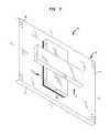
- FIG. 1is a perspective view of an assembly according to one embodiment of the present invention
- FIG. 2is a perspective view of a package according to one embodiment of the present invention.
- FIG. 3is a top schematic view of the embodiment of FIG. 2 ;
- FIG. 4is a cross-sectional view of the embodiment of FIG. 2 attached to a circuit panel;
- FIG. 5is a cross-sectional view of a stacked package according to one embodiment of the present invention.
- FIG. 6is a perspective view of an assembly according to an additional embodiment of the present invention.
- FIG. 7is a cross-sectional view of a package according to an additional embodiment of the present invention.
- FIG. 8is a cross-sectional view of an alternate embodiment of a stacked package according to the present invention.
- FIG. 9is a cross-sectional view of a package according to an alternate embodiment of the present invention taken along a first axis;
- FIG. 10is a cross-sectional view of the embodiment of FIG. 9 taken along a second axis perpendicular to the first axis;
- FIG. 11is a cross-sectional view of a package according to an alternate embodiment of the present invention.
- FIG. 12is cross-sectional view of a package according to an additional embodiment of the present invention.
- FIG. 13is a cross-sectional view of a package according to an additional embodiment of the present invention.
- a microelectronic assembly 10includes a first microelectronic element 12 and a second microelectronic element 14 , as shown in FIG. 1 .
- the first microelectronic element 12 and the second microelectronic element 14may be semiconductor chips, interposers, circuit panels, modules, integrated passives on chip (IPOCs) or various other passive and active elements.
- IPOCsintegrated passives on chip
- the first microelectronic element 12includes a first surface 16 , an oppositely-facing second surface 18 and edges 20 , 21 adjacent the first surface 16 and the second surface 18 .
- the edges 20 , 21are part of a perimeter 23 that extends around the first microelectronic element 12 .
- the second microelectronic element 14includes a first surface 22 , an oppositely-facing second surface 24 and edges 26 , 27 adjacent the first surface and the second surface.
- the edges 26 , 27are part of a perimeter 28 that extends around the second microelectronic element 14 .
- the first microelectronic element 12overlies the second microelectronic element 14 , such that the second surface of the first microelectronic element 12 faces the first surface 22 of the second microelectronic element 14 .
- edges 20 and 21 of the first microelectronic element 12extend outwardly past the perimeter 28 of the second microelectronic element 12
- edges 26 and 27 of the second microelectronic element 14extend outwardly past the perimeter 23 of the first microelectronic element 12 .
- the first microelectronic element 12has a length L and a width W and the second microelectronic element 14 has a length L′ and a width W′.
- the lengths L and L′have a dimension that is greater than the dimension of widths W and W′, although this is not required.
- the length L of the first microelectronic element 12is transverse to the length L′ of the second microelectronic element 14 and more preferably the two lengths L and L′ are orthogonal to one another. For ease of illustration, FIG.
- the two microelectronic elements 12 , 14are stacked onto one another in a direction along a Z-axis.
- the coordinate system described hereinis only used for ease of illustration and does not refer to any gravitational positioning. Descriptive words such as “top” “bottom” “upper” and “lower” are similarly only used for illustration purposes only.
- FIG. 1also illustrates examples of some of the various features that may be included within the microelectronic assembly 10 .
- First microelectronic element 12may include a plurality of contacts 32 exposed at its first surface 16 .
- the contacts 32may project above the first surface 16 , be recessed within the first surface or be planar with the surface of the first microelectronic element 12 .
- Second microelectronic element 14also includes a plurality of contacts 34 exposed at the first surface 22 of the second microelectronic element 14 . Similar to the contacts 32 of the first microelectronic element 12 , the contacts 34 of the second microelectronic element 14 enable an electrical connection between the second microelectronic element 14 and another microelectronic element.
- the first microelectronic element 12may be connected to the second microelectronic element 14 by an encapsulant material or underfill 36 .
- the encapsulant material 36may include an epoxy, silicone or other adhesive material.
- the underfill 36may also be a thermally-conductive material that permits heat to dissipate from the microelectronic elements 12 , 14 .
- the first microelectronic element 12may be connected or attached to the second microelectronic element 14 by any method known to those in the art including but not limited to features that enable the elements to be snap fitted to one another or even formed integrally together.
- microelectronic elements 12 , 14may also be temporarily affixed to one another by various vices, molds and the like, while various features described herein are added to the assembly. After the features have been added, the vices may be removed and an encapsulant material applied to the assembly to thereby provide stability and structure to the microelectronic assembly 10 .
- the first microelectronic element 12may also include edges 20 and 21 , as well as edges 37 and 38 .
- the second microelectronic element 14may also include edges 26 and 27 , as well as edges 39 and 40 .
- edge 20 of the first microelectronic elementis parallel to edge 39 of the second microelectronic element 14 in the X-direction.
- edge 21is also parallel to edge 39 of the second microelectronic element 14 .
- either one or both of the edges 37 and 38 of the first microelectronic element 12may be parallel to edges 26 and 27 of the second microelectronic element 14 in the Y-direction.
- the microelectronic element assembly 10may include a substrate 40 having a top surface 42 and an oppositely-facing bottom surface 44 , as shown in FIG. 2 .
- the substratemay include a layer of polyimide or other dielectric material.
- the substratemay also be formed by any known composition known by those in the art.
- a solder mask layer(not shown) may be disposed on the single metal layer.
- a package 41may include the assembly of FIG. 1 connected with the substrate 40 , as shown in FIG. 2 .
- Substrate 40is positioned overlying the first microelectronic element 12 such that the bottom surface 44 of the substrate faces the first surface 16 of the first microelectronic element 12 .
- An adhesive material 46 or underfillmay be used to connect the first microelectronic element 12 to the bottom surface 44 of the substrate 40 .
- the encapsulant materialmay be replaced by an adhesive or thermal-conductive layer or an element that performs both functions.
- Substrate 40includes a plurality of terminals 48 exposed at the top surface 42 and exposed at the bottom surface 44 of the substrate through hole 49 , best shown in FIG. 4 .
- the terminals 48may be positioned along a perimeter P of the substrate and more preferably the terminals are positioned at the corners of the substrate.
- the substrate 40may include bonding contacts 50 exposed at the top surface 42 of the substrate. At least some of the bonding contacts 50 are electrically connected to at least some of the terminals 48 by traces 52 disposed on or within the substrate 40 .
- the electrical interconnecting elementssuch as terminals 48 , bonding contacts 50 , and traces 52 of the substrate 40 may be formed in two or more layers. In the embodiment of FIGS. 2 and 3 , the interconnecting elements are formed using a single layer of metal.
- Substrate 40also includes a plurality of apertures 54 extending from the top surface 42 to the bottom surface 44 .
- the apertures 54are aligned with the contacts 32 and 34 of the first microelectronic element and second microelectronic element, respectively. Therefore, the apertures overlie and allow access to the respective microelectronic elements.
- Each of the apertures 54is partially defined by an edge 56 .
- an electrical interconnection elementmay be included in the microelectronic assembly 41 between contacts 32 , 34 and bonding contacts 50 .
- the interconnection elementmay be in the form of wire leads 55 extending from contacts 32 , 34 , through apertures 54 , across edges 56 to bonding contacts 50 .
- the wire leads 55connect the contacts 32 , 34 of the first microelectronic element 12 and the second microelectronic element 14 to the bonding contacts 50 of the substrate 40 .
- the bonding contacts 50are connected to terminals 48 of the substrate by traces 52 .
- the traces 52include various sections, angles and turns as well as runs 53 extending in an edgewise direction denoted by the arrow E parallel to an edge 56 of the substrate bounding a slot.
- each row of bonding contacts 50is disposed in rows 51 near apertures 54 .
- Each row of bonding contactsextends in an edgewise direction, parallel to the adjacent edge of the slot.
- a row 51 A of bonding contacts adjacent to slot 54 Aextends in the edgewise direction E adjacent the edge 56 of apertures 54 A
- the bonding contacts in row 51 Bextend in an edgewise direction parallel to the edge 56 of slot 54 B.
- the bonding contacts of row 51 Aare connected in an arrangement referred to herein as a “trace-proximate” arrangement, with at least some of the runs 53 of traces 52 connected to the bonding contacts 50 extending between the bonding contacts and the edge 56 of the adjacent apertures 54 A.
- the bonding contacts of row 51 Aare connected to a group of terminals 48 A close to one end of the aperture.
- the bonding contact 50 Aa closest to this group of terminalsis connected to the run 53 Aa furthest from the edge 56 , which in turn is connected to terminal 48 Aa.
- the bonding contact 50 Ac furthest from this group of terminalsis connected to the run 53 Ac closest to edge 56 , which in turn is connected to terminal 48 Ac.
- the other bonding contactsare connected to trace runs, and hence to terminals in group 48 A.
- the order of connection to the terminalscorresponds to the order of contact position in edgewise direction E A , i.e., the edgewise direction along edge 56 A away from terminal group 48 A.
- the bonding contacts and traces of row 51 Bare connected in the reverse arrangement, referred to herein as a “trace-remote” arrangement.
- the trace-remote arrangementat least some of the runs 53 of traces 52 connected to the bonding contacts of the row lie between the runs connected to those contacts and the edge 56 of the adjacent aperture 54 B.
- the bonding contacts of row 51 Bare also connected to the same group of terminals 48 A.
- the bonding contact 50 Ba furthest from the group of terminals 48 Ais connected to the run 53 Ba furthest from edge 56 B, which in turn is connected to terminal 48 Aa.
- the bonding contact 50 Bc closest to the group of terminals 48 Ais connected to the run 53 Bc closest to edge 56 B, which in turn is connected to terminal 48 Ac.
- the other bonding contacts in row 51 Bare connected to trace runs, and hence to terminals in group 48 A in order according to their contact position.
- the order of connection to the terminalscorresponds to the order of contact position in edgewise direction E B , i.e., the edgewise direction along edge 56 B towards terminal group 48 A.
- This arrangementprovides two rows of bonding terminals having identical order of connection to terminals, but running in two different edgewise directions, without crossovers, so that all of the traces can be formed in a single metal layer.
- the identically-connected rows of bonding terminalsallow for common connections to be made to identical chips. For example, the contact labeled “IO7” on chip 12 is connected to bonding contact 50 Ba and hence to terminal 48 a , whereas the identical contact 34 , labeled 107 on chip 14 is connected to bonding contact 50 Aa and hence to the same terminal 48 a.
- Wire leads 55 formed by a wire-bonding processconnect the bonding contacts to the contacts 32 and 34 of the chips.
- the wire bonds associated with each row of bonding contactsextend across the adjacent edge 56 , and extend through the adjacent aperture 54 to one of the chips.
- the wire bonds associated with the bonding contacts of rows 51 A and 51 Cextend through slots 54 A and 54 C.
- Some of the wire bondsextend across the runs 53 of some of the traces.
- the wire bonds 55 associated with bonding contacts of rows 51 A and 51 C, having a trace-proximate arrangementextend across associated runs. As best seen in FIG. 4 , the wire bonds loop up and over the traces.
- the wire bonds associated with some of the contacts in row 51 D( FIG.
- FIG. 3depicts the chip enable contacts (labeled “CE”) as connected to all of the chip-enable bonding contacts 50 ′; in practice, each chip enable contact is connected to only one chip-enable bonding contact, and hence connected to only one terminal in group 48 C. Different chips are connected to different terminals in group 48 C.
- CEchip enable contacts
- the microelectronic assembly 41may include an encapsulant material 60 adhered to the top surface 42 of the substrate 40 .
- the encapsulant material 60protects and maintains the integrity of the wire leads 55 interconnecting the bonding contacts 50 to the contacts 32 , 34 of the microelectronic elements 12 , 14 .
- the terminals 48enable the microelectronic assembly 41 to be electrically connected to a microelectronic element such as circuit panel 62 .
- the circuit panel 62includes terminals 64 exposed at a surface of the circuit panel.
- An electrical interconnection, such as a mass of solder 66may be used to electrically connect terminals 48 of the substrate 42 to terminals 64 of the circuit panel 62 .
- the electrical interconnections between the package and the circuit panel 62may be made without interfering with the positioning of the first microelectronic element 12 and second microelectronic element 14 .
- An additional encapsulant 70may be disposed about the first microelectronic element 12 and second microelectronic element 14 to not only connect the microelectronic elements to the substrate 40 but also to maintain the integrity of the wire leads 55 extending through the apertures 54 of the substrate.
- the microelectronic assembly 41may be positioned with a second microelectronic assembly 141 overlying the assembly.
- the second microelectronic assembly 141may be substantially similar to the first microelectronic assembly 41 with similar features and elements.
- the second microelectronic assembly 141preferably has terminals 148 exposed at a top surface 142 and exposed at a bottom surface 144 of a substrate 140 .
- the terminals 148may be electrically connected to the terminals 48 of the first microelectronic assembly 41 by, for example, masses of solder 166 .
- terminals 48 , 148may not be exposed at respective top surfaces 42 , 142 if not required.
- An encapsulantmay be adhered to the top surface 142 of the substrate 140 to protect and maintain the integrity of the wire leads 155 .
- a first microelectronic element 212may overlie a second microelectronic element 214 with an edge 238 of the first microelectronic element 212 parallel with an edge 227 of the second microelectronic element 214 in the X-direction.
- Edges 220 , 221 of the first microelectronic element 212may extend outwardly past edges 239 and 240 of the second microelectronic element 214 , respectively.
- both edges 220 and 221are shown extending outwardly past the respective edges of the second microelectronic element, this is not required and only one edge of the microelectronic element may extend outwardly past an edge of the second microelectronic element.
- the microelectronic package 210 shown in FIG. 6may include various features and elements included in previous embodiments discussed herein. For instance, a substrate similar to substrate 40 may be included with the microelectronic package 210 to create an assembly.
- microelectronic elementshaving a rectangular shape.
- the microelectronic elementsmay have any shape, including but not limited to, square, triangular, oval and circular.
- wire leads 355may extend across edges 341 of substrate 340 , to thereby electrically connect contacts 332 , 334 exposed on the first microelectronic element 312 and second microelectronic element 314 to bonding contacts 350 exposed on substrate 340 .
- An encapsulant materialmay be placed around the microelectronic semiconductor package 310 to maintain the rigidity and stability of the package.
- the microelectronic assembly 41 of FIG. 3may be stacked in facing relationship to a second microelectronic assembly 441 .
- the second microelectronic assembly 441may include many of the same features and elements illustrated in reference to previous embodiments discussed herein. For ease of illustration, some of these features are not illustrated in the figure.
- the terminals 48 of the first microelectronic assembly 41 and terminals 448 of the second microelectronic assembly 441also face one another.
- An electrical connection 466may be disposed between the terminals 48 , 448 in order to connect them and create a stacked microelectronic package.
- Contact pads(not shown) may be positioned on substrate 40 in order to connect the package to a circuit panel, for example.
- microelectronic assembly 541may include a first microelectronic element 512 and a second microelectronic element 514 as shown in FIGS. 9 and 10 .
- the first microelectronic element 512includes a first surface 516 and an oppositely-facing second surface 518 .
- the second microelectronic element 514also includes a first surface 520 and an oppositely-facing second surface 522 .
- the microelectronic assembly 541also includes substrate 540 having a first surface 542 and a second surface 544 .
- the first microelectronic element 512is positioned overlying the substrate 540 such that the second surface 518 of the first microelectronic element confronts the top surface 542 of the substrate 540 .
- the second microelectronic element 514is positioned underlying the substrate 540 , such that the second surface 522 of the microelectronic element confronts the bottom surface 544 of the substrate.
- the microelectronic elements 512 , 514may be attached to the substrate 540 by an underfill or encapsulant 560 .
- the two microelectronic elements 512 , 514are arranged similar to previous embodiments discussed herein except that the substrate 540 is positioned between the elements.
- at least one of the edges 520 , 521 of the first microelectronic element 512extends outwardly beyond one of the edges 539 , 540 of the second microelectronic element 514 .
- at least one of the edges 526 , 527 of the second microelectronic element 514extends outwardly past one of the edges 537 , 538 of the second microelectronic element 514 .
- the two microelectronic elementsare positioned in a criss-cross relationship with the substrate disposed therebetween.
- the first microelectronic element 512 and the second microelectronic element 514also preferably include contacts 532 , 534 exposed at their respective second surfaces 518 , 522 .
- the contacts 532 , 534are preferably aligned with apertures 554 extending from the top surface 542 to the bottom surface 544 of the substrate 540 .
- the substrate 540further includes terminals 548 exposed at either, or both of the top surfaces 542 or the bottom surface 544 and bonding contacts 50 exposed at both the top and bottom surfaces.
- At least some of the bonding contacts 550are electrically connected with at least some of the terminals 548 by traces 552 as shown in FIG. 10 . For ease of illustration, only some of the traces connecting the bonding contacts 550 to the terminals 548 are illustrated.
- the metal layermay be disposed at the bottom surface 544 of substrate 540 with bonding contacts 550 exposed at the top surface 542 and the bottom surface 544 of the substrate.
- electrical interconnectionsi.e., wire leads 555
- the wire leads 555extend from the contacts 532 , 534 through the apertures 554 of the substrate until attaching to the bonding contacts 550 . Therefore, the wire leads 555 extend from microelectronic elements 512 or 514 from one surface of the substrate 540 the top surface 542 for the first microelectronic element, and the bottom surface 544 for the second microelectronic element 514 to the opposite surface of the substrate.
- wire leads 555attach to contacts 332 of the first microelectronic element 512 adjacent the top surface 542 and extend through an aperture 554 across edge 556 to the opposing bottom surface 544 of the substrate 540 , specifically the bonding contacts 550 disposed on the bottom surface.
- wire leads 555 connected to the second microelectronic elementextend from contacts 534 adjacent the bottom surface 544 of the substrate to the top surface 542 .
- An encapsulant material 561may be disposed over the wire leads 555 to protect them.
- microelectronic assembly 541may be stacked onto a similar assembly or various other assemblies to form a stacked package.
- the microelectronic assembly 641may include a substrate 640 and first microelectronic element 612 formed similarly to the first microelectronic element and substrate of FIGS. 9 and 10 .
- the second microelectronic element 614differs from the one illustrated in FIGS. 9 and 10 in that it is electrically interconnected to the substrate 640 at the bottom surface 644 of the substrate.
- the second microelectronic element 614preferably may include contacts 634 exposed along a second surface 622 of the second microelectronic element. The contacts may be electrically connected to the substrate 540 by either a ball-grid array, stud bumps, wire leads or additional electrical connecting mechanisms.
- the substrate 640includes bonding contacts 50 exposed at its second surface 644 that can be interconnected to the contacts 634 of the second microelectronic element.
- the microelectronic assembly 741may be similarly constructed to the previous embodiments except that a substrate 740 includes a two metal layer construction wherein a first metal lay 790 is exposed at a top surface 742 of the substrate 740 and a second metal layer 791 is disposed at a bottom surface 744 of the substrate.
- the microelectronic assembly 741includes a first microelectronic element 712 and a second microelectronic element 714 .
- Each of the microelectronic elementsmay be attached to the substrate 740 in a method already discussed herein.
- One benefit of having a two metal layeris that bonding wires 755 connecting contacts 732 exposed at a first surface of a respective microelectronic element 712 , 714 , does not have to extend through the substrate 740 and then back around and through the substrate 740 once again in order to be bonded to the bonding contact 750 of the substrate 740 .
- first metal layer 742 and the second metal layer 745may each include a plurality of terminals, traces and bonding contacts as discussed with reference to previous embodiments herein.
- the present inventionalso contemplates a situation wherein either a single metal layer or a two metal layer are exposed within a substrate.
- the metal layer or layersmay be exposed at one or both surfaces of the substrate depending on the specific requirements.
- a microelectronic assembly 841may be constructed similar to any of the embodiments herein, but also include electrically-conductive posts or pillars 898 instead of or in combination with terminals.
- the pillars 898extend downwardly from the substrate 840 .
- the pillars 898 in combination with the traces 852 and bonding contacts 850may be constructed as disclosed in commonly assigned U.S. patent application Ser. Nos. 10/985,119, 10/985,126 and 11/014,439, the disclosures of which are hereby incorporated herein by reference.
- the second microelectronic element 614 of FIG. 11may have contacts disposed along the first surface 620 of the second microelectronic element.
- the contactsmay be attached to bonding contacts exposed at the bottom surface 644 of the substrate 640 using wire leads.
- the substratecan optionally include additional trace layers.
- the apertures 54have been shown as elongated slots, they may have any configuration.
Landscapes
- Engineering & Computer Science (AREA)
- Microelectronics & Electronic Packaging (AREA)
- Power Engineering (AREA)
- Computer Hardware Design (AREA)
- General Physics & Mathematics (AREA)
- Condensed Matter Physics & Semiconductors (AREA)
- Physics & Mathematics (AREA)
- Structures For Mounting Electric Components On Printed Circuit Boards (AREA)
- Wire Bonding (AREA)
- Structures Or Materials For Encapsulating Or Coating Semiconductor Devices Or Solid State Devices (AREA)
- Micromachines (AREA)
- Apparatus For Radiation Diagnosis (AREA)
- Led Device Packages (AREA)
Abstract
Description
Claims (18)
Priority Applications (2)
| Application Number | Priority Date | Filing Date | Title |
|---|---|---|---|
| US13/246,242US8890327B2 (en) | 2005-12-01 | 2011-09-27 | Stacked microelectronic packages having at least two stacked microelectronic elements adjacent one another |
| US14/529,279US9627366B2 (en) | 2005-12-01 | 2014-10-31 | Stacked microelectronic packages having at least two stacked microelectronic elements adjacent one another |
Applications Claiming Priority (2)
| Application Number | Priority Date | Filing Date | Title |
|---|---|---|---|
| US11/291,398US8026611B2 (en) | 2005-12-01 | 2005-12-01 | Stacked microelectronic packages having at least two stacked microelectronic elements adjacent one another |
| US13/246,242US8890327B2 (en) | 2005-12-01 | 2011-09-27 | Stacked microelectronic packages having at least two stacked microelectronic elements adjacent one another |
Related Parent Applications (1)
| Application Number | Title | Priority Date | Filing Date |
|---|---|---|---|
| US11/291,398ContinuationUS8026611B2 (en) | 2005-12-01 | 2005-12-01 | Stacked microelectronic packages having at least two stacked microelectronic elements adjacent one another |
Related Child Applications (1)
| Application Number | Title | Priority Date | Filing Date |
|---|---|---|---|
| US14/529,279DivisionUS9627366B2 (en) | 2005-12-01 | 2014-10-31 | Stacked microelectronic packages having at least two stacked microelectronic elements adjacent one another |
Publications (2)
| Publication Number | Publication Date |
|---|---|
| US20120013028A1 US20120013028A1 (en) | 2012-01-19 |
| US8890327B2true US8890327B2 (en) | 2014-11-18 |
Family
ID=37763826
Family Applications (3)
| Application Number | Title | Priority Date | Filing Date |
|---|---|---|---|
| US11/291,398ActiveUS8026611B2 (en) | 2005-12-01 | 2005-12-01 | Stacked microelectronic packages having at least two stacked microelectronic elements adjacent one another |
| US13/246,242Expired - Fee RelatedUS8890327B2 (en) | 2005-12-01 | 2011-09-27 | Stacked microelectronic packages having at least two stacked microelectronic elements adjacent one another |
| US14/529,279ActiveUS9627366B2 (en) | 2005-12-01 | 2014-10-31 | Stacked microelectronic packages having at least two stacked microelectronic elements adjacent one another |
Family Applications Before (1)
| Application Number | Title | Priority Date | Filing Date |
|---|---|---|---|
| US11/291,398ActiveUS8026611B2 (en) | 2005-12-01 | 2005-12-01 | Stacked microelectronic packages having at least two stacked microelectronic elements adjacent one another |
Family Applications After (1)
| Application Number | Title | Priority Date | Filing Date |
|---|---|---|---|
| US14/529,279ActiveUS9627366B2 (en) | 2005-12-01 | 2014-10-31 | Stacked microelectronic packages having at least two stacked microelectronic elements adjacent one another |
Country Status (5)
| Country | Link |
|---|---|
| US (3) | US8026611B2 (en) |
| JP (1) | JP5547893B2 (en) |
| KR (2) | KR101409946B1 (en) |
| CN (1) | CN101322246B (en) |
| WO (1) | WO2007064779A1 (en) |
Cited By (1)
| Publication number | Priority date | Publication date | Assignee | Title |
|---|---|---|---|---|
| US9859263B2 (en) | 2015-10-30 | 2018-01-02 | Samsung Electronics Co., Ltd. | Semiconductor package |
Families Citing this family (13)
| Publication number | Priority date | Publication date | Assignee | Title |
|---|---|---|---|---|
| TWI335652B (en)* | 2007-04-04 | 2011-01-01 | Unimicron Technology Corp | Stacked packing module |
| US7994644B2 (en)* | 2007-06-01 | 2011-08-09 | Tessera, Inc. | Package stacking through rotation |
| KR101003568B1 (en)* | 2007-11-14 | 2010-12-22 | 산요 세미컨덕터 컴퍼니 리미티드 | Semiconductor Modules and Imaging Devices |
| US8390083B2 (en) | 2009-09-04 | 2013-03-05 | Analog Devices, Inc. | System with recessed sensing or processing elements |
| US8569884B2 (en) | 2011-08-15 | 2013-10-29 | Tessera, Inc. | Multiple die in a face down package |
| US8680684B2 (en)* | 2012-01-09 | 2014-03-25 | Invensas Corporation | Stackable microelectronic package structures |
| US9847462B2 (en) | 2013-10-29 | 2017-12-19 | Point Engineering Co., Ltd. | Array substrate for mounting chip and method for manufacturing the same |
| KR102161776B1 (en)* | 2014-03-28 | 2020-10-06 | 에스케이하이닉스 주식회사 | Stack package |
| JP6507779B2 (en)* | 2015-03-26 | 2019-05-08 | セイコーエプソン株式会社 | Electro-optical device, method of manufacturing electro-optical device, and electronic apparatus |
| US9666558B2 (en) | 2015-06-29 | 2017-05-30 | Point Engineering Co., Ltd. | Substrate for mounting a chip and chip package using the substrate |
| US20180114786A1 (en)* | 2016-10-21 | 2018-04-26 | Powertech Technology Inc. | Method of forming package-on-package structure |
| KR102149387B1 (en) | 2019-02-13 | 2020-08-28 | 삼성전기주식회사 | Electronic component module |
| US20240096859A1 (en)* | 2022-08-19 | 2024-03-21 | Google Llc | Socket To Support High Performance Multi-die ASICs |
Citations (34)
| Publication number | Priority date | Publication date | Assignee | Title |
|---|---|---|---|---|
| US4956694A (en) | 1988-11-04 | 1990-09-11 | Dense-Pac Microsystems, Inc. | Integrated circuit chip stacking |
| JPH02312265A (en) | 1989-05-26 | 1990-12-27 | Mitsubishi Electric Corp | Semiconductor device |
| JPH04155954A (en) | 1990-10-19 | 1992-05-28 | Nec Kyushu Ltd | Semiconductor device |
| US5198888A (en) | 1987-12-28 | 1993-03-30 | Hitachi, Ltd. | Semiconductor stacked device |
| JPH05121643A (en) | 1990-12-05 | 1993-05-18 | Matra Marconi Space Fr | Solid state memory module and memory device including such a module |
| US5325268A (en) | 1993-01-28 | 1994-06-28 | National Semiconductor Corporation | Interconnector for a multi-chip module or package |
| US5325628A (en) | 1991-09-06 | 1994-07-05 | Yingling Dan C | Automatic door operator |
| US5468994A (en) | 1992-12-10 | 1995-11-21 | Hewlett-Packard Company | High pin count package for semiconductor device |
| WO1996020550A1 (en) | 1994-12-23 | 1996-07-04 | National Semiconductor Corporation | Lead frame for handling crossing bonding wires |
| US5841191A (en) | 1997-04-21 | 1998-11-24 | Lsi Logic Corporation | Ball grid array package employing raised metal contact rings |
| US5861666A (en) | 1995-08-30 | 1999-01-19 | Tessera, Inc. | Stacked chip assembly |
| US5998864A (en)* | 1995-05-26 | 1999-12-07 | Formfactor, Inc. | Stacking semiconductor devices, particularly memory chips |
| US6020629A (en) | 1998-06-05 | 2000-02-01 | Micron Technology, Inc. | Stacked semiconductor package and method of fabrication |
| US6072233A (en) | 1998-05-04 | 2000-06-06 | Micron Technology, Inc. | Stackable ball grid array package |
| US6215193B1 (en) | 1999-04-21 | 2001-04-10 | Advanced Semiconductor Engineering, Inc. | Multichip modules and manufacturing method therefor |
| US6252305B1 (en) | 2000-02-29 | 2001-06-26 | Advanced Semiconductor Engineering, Inc. | Multichip module having a stacked chip arrangement |
| US20020043709A1 (en) | 2000-10-13 | 2002-04-18 | Yeh Nai Hua | Stackable integrated circuit |
| US6388333B1 (en) | 1999-11-30 | 2002-05-14 | Fujitsu Limited | Semiconductor device having protruding electrodes higher than a sealed portion |
| US6404648B1 (en) | 2001-03-30 | 2002-06-11 | Hewlett-Packard Co. | Assembly and method for constructing a multi-die integrated circuit |
| US20020171136A1 (en) | 2001-05-15 | 2002-11-21 | Fujitsu Limited | Semiconductor device with stack of semiconductor chips |
| US20030025199A1 (en) | 2001-08-01 | 2003-02-06 | Chi-Chuan Wu | Super low profile package with stacked dies |
| US20030047813A1 (en) | 2001-08-30 | 2003-03-13 | Bernd Goller | Electronic component with at least two stacked semiconductor chips and method for fabricating the electronic component |
| DE10227305A1 (en) | 2002-06-19 | 2003-09-04 | Siemens Dematic Ag | Electrical multiple layer component module used in polymer stud grid array technology comprises a second three-dimensional substrate arranged on first three-dimensional substrate with intermediate connections connected to contacts |
| US20030183917A1 (en) | 2002-02-07 | 2003-10-02 | Macronix International Co., Ltd. | Stacked semiconductor packaging device |
| US20040046239A1 (en) | 2002-09-11 | 2004-03-11 | International Business Machines Corporation | Stacked package for integrated circuits |
| US20040061146A1 (en) | 2002-09-30 | 2004-04-01 | Shiann-Tsong Tsai | Multi-chip semiconductor package and fabrication method thereof |
| US20040262774A1 (en)* | 2003-06-27 | 2004-12-30 | In-Ku Kang | Multi-chip packages having a plurality of flip chips and methods of manufacturing the same |
| US20050087855A1 (en) | 1990-09-24 | 2005-04-28 | Tessera, Inc. | Microelectronic component and assembly having leads with offset portions |
| US20050205979A1 (en) | 1999-08-24 | 2005-09-22 | Shin Won S | Semiconductor package and method for fabricating the same |
| US20050253229A1 (en) | 2002-11-07 | 2005-11-17 | Sharp Kabushiki Kaisha | Semiconductor device and manufacturing method of same |
| US20060290005A1 (en)* | 2005-06-28 | 2006-12-28 | Jochen Thomas | Multi-chip device and method for producing a multi-chip device |
| US7176043B2 (en) | 2003-12-30 | 2007-02-13 | Tessera, Inc. | Microelectronic packages and methods therefor |
| US7709968B2 (en) | 2003-12-30 | 2010-05-04 | Tessera, Inc. | Micro pin grid array with pin motion isolation |
| US8207604B2 (en) | 2003-12-30 | 2012-06-26 | Tessera, Inc. | Microelectronic package comprising offset conductive posts on compliant layer |
Family Cites Families (3)
| Publication number | Priority date | Publication date | Assignee | Title |
|---|---|---|---|---|
| US5721452A (en)* | 1995-08-16 | 1998-02-24 | Micron Technology, Inc. | Angularly offset stacked die multichip device and method of manufacture |
| US6388833B1 (en)* | 1998-06-29 | 2002-05-14 | Western Digital Technologies, Inc. | Method for manufacturing a disk drive having an overwriteable clock track |
| ES2426255T3 (en)* | 2002-06-28 | 2013-10-22 | Boston Scientific Neuromodulation Corporation | Microstimulator that has a built-in power source and a two-way telemetry system |
- 2005
- 2005-12-01USUS11/291,398patent/US8026611B2/enactiveActive
- 2006
- 2006-11-30KRKR1020087013790Apatent/KR101409946B1/enactiveActive
- 2006-11-30WOPCT/US2006/045817patent/WO2007064779A1/enactiveApplication Filing
- 2006-11-30JPJP2008543449Apatent/JP5547893B2/ennot_activeExpired - Fee Related
- 2006-11-30KRKR1020137029068Apatent/KR101479440B1/enactiveActive
- 2006-11-30CNCN2006800452483Apatent/CN101322246B/enactiveActive
- 2011
- 2011-09-27USUS13/246,242patent/US8890327B2/ennot_activeExpired - Fee Related
- 2014
- 2014-10-31USUS14/529,279patent/US9627366B2/enactiveActive
Patent Citations (37)
| Publication number | Priority date | Publication date | Assignee | Title |
|---|---|---|---|---|
| US5198888A (en) | 1987-12-28 | 1993-03-30 | Hitachi, Ltd. | Semiconductor stacked device |
| US4956694A (en) | 1988-11-04 | 1990-09-11 | Dense-Pac Microsystems, Inc. | Integrated circuit chip stacking |
| JPH02312265A (en) | 1989-05-26 | 1990-12-27 | Mitsubishi Electric Corp | Semiconductor device |
| US20050087855A1 (en) | 1990-09-24 | 2005-04-28 | Tessera, Inc. | Microelectronic component and assembly having leads with offset portions |
| JPH04155954A (en) | 1990-10-19 | 1992-05-28 | Nec Kyushu Ltd | Semiconductor device |
| JPH05121643A (en) | 1990-12-05 | 1993-05-18 | Matra Marconi Space Fr | Solid state memory module and memory device including such a module |
| US5325628A (en) | 1991-09-06 | 1994-07-05 | Yingling Dan C | Automatic door operator |
| US5468994A (en) | 1992-12-10 | 1995-11-21 | Hewlett-Packard Company | High pin count package for semiconductor device |
| US5325268A (en) | 1993-01-28 | 1994-06-28 | National Semiconductor Corporation | Interconnector for a multi-chip module or package |
| WO1996020550A1 (en) | 1994-12-23 | 1996-07-04 | National Semiconductor Corporation | Lead frame for handling crossing bonding wires |
| US5998864A (en)* | 1995-05-26 | 1999-12-07 | Formfactor, Inc. | Stacking semiconductor devices, particularly memory chips |
| US5861666A (en) | 1995-08-30 | 1999-01-19 | Tessera, Inc. | Stacked chip assembly |
| US5841191A (en) | 1997-04-21 | 1998-11-24 | Lsi Logic Corporation | Ball grid array package employing raised metal contact rings |
| US6072233A (en) | 1998-05-04 | 2000-06-06 | Micron Technology, Inc. | Stackable ball grid array package |
| US6268649B1 (en) | 1998-05-04 | 2001-07-31 | Micron Technology, Inc. | Stackable ball grid array package |
| US6020629A (en) | 1998-06-05 | 2000-02-01 | Micron Technology, Inc. | Stacked semiconductor package and method of fabrication |
| US6215193B1 (en) | 1999-04-21 | 2001-04-10 | Advanced Semiconductor Engineering, Inc. | Multichip modules and manufacturing method therefor |
| US20050205979A1 (en) | 1999-08-24 | 2005-09-22 | Shin Won S | Semiconductor package and method for fabricating the same |
| US6388333B1 (en) | 1999-11-30 | 2002-05-14 | Fujitsu Limited | Semiconductor device having protruding electrodes higher than a sealed portion |
| US20020074630A1 (en) | 1999-11-30 | 2002-06-20 | Fujitsu Limited | Semiconductor device having protruding electrodes higher than a sealed portion |
| US6252305B1 (en) | 2000-02-29 | 2001-06-26 | Advanced Semiconductor Engineering, Inc. | Multichip module having a stacked chip arrangement |
| US20020043709A1 (en) | 2000-10-13 | 2002-04-18 | Yeh Nai Hua | Stackable integrated circuit |
| US6404648B1 (en) | 2001-03-30 | 2002-06-11 | Hewlett-Packard Co. | Assembly and method for constructing a multi-die integrated circuit |
| US20020171136A1 (en) | 2001-05-15 | 2002-11-21 | Fujitsu Limited | Semiconductor device with stack of semiconductor chips |
| US20030025199A1 (en) | 2001-08-01 | 2003-02-06 | Chi-Chuan Wu | Super low profile package with stacked dies |
| US20030047813A1 (en) | 2001-08-30 | 2003-03-13 | Bernd Goller | Electronic component with at least two stacked semiconductor chips and method for fabricating the electronic component |
| US6710455B2 (en) | 2001-08-30 | 2004-03-23 | Infineon Technologies Ag | Electronic component with at least two stacked semiconductor chips and method for fabricating the electronic component |
| US20030183917A1 (en) | 2002-02-07 | 2003-10-02 | Macronix International Co., Ltd. | Stacked semiconductor packaging device |
| DE10227305A1 (en) | 2002-06-19 | 2003-09-04 | Siemens Dematic Ag | Electrical multiple layer component module used in polymer stud grid array technology comprises a second three-dimensional substrate arranged on first three-dimensional substrate with intermediate connections connected to contacts |
| US20040046239A1 (en) | 2002-09-11 | 2004-03-11 | International Business Machines Corporation | Stacked package for integrated circuits |
| US20040061146A1 (en) | 2002-09-30 | 2004-04-01 | Shiann-Tsong Tsai | Multi-chip semiconductor package and fabrication method thereof |
| US20050253229A1 (en) | 2002-11-07 | 2005-11-17 | Sharp Kabushiki Kaisha | Semiconductor device and manufacturing method of same |
| US20040262774A1 (en)* | 2003-06-27 | 2004-12-30 | In-Ku Kang | Multi-chip packages having a plurality of flip chips and methods of manufacturing the same |
| US7176043B2 (en) | 2003-12-30 | 2007-02-13 | Tessera, Inc. | Microelectronic packages and methods therefor |
| US7709968B2 (en) | 2003-12-30 | 2010-05-04 | Tessera, Inc. | Micro pin grid array with pin motion isolation |
| US8207604B2 (en) | 2003-12-30 | 2012-06-26 | Tessera, Inc. | Microelectronic package comprising offset conductive posts on compliant layer |
| US20060290005A1 (en)* | 2005-06-28 | 2006-12-28 | Jochen Thomas | Multi-chip device and method for producing a multi-chip device |
Non-Patent Citations (5)
| Title |
|---|
| International Search Report for Application No. PCT/US2006/045817 dated Apr. 27, 2007. |
| International Written Opinion for Application No. PCT/US2006/045817 dated Apr. 27, 2007. |
| Korean Office Action for Application No. 10-2008-7013790 dated May 1, 2013. |
| Office Action from corresponding Chinese Application 200680045248, dated Jul. 10, 2009. |
| Office Action from corresponding Japanese Application 2008-543449 dated Feb. 10, 2012. |
Cited By (2)
| Publication number | Priority date | Publication date | Assignee | Title |
|---|---|---|---|---|
| US9859263B2 (en) | 2015-10-30 | 2018-01-02 | Samsung Electronics Co., Ltd. | Semiconductor package |
| US10141293B2 (en) | 2015-10-30 | 2018-11-27 | Samsung Electronics Co., Ltd. | Semiconductor package |
Also Published As
| Publication number | Publication date |
|---|---|
| JP5547893B2 (en) | 2014-07-16 |
| WO2007064779A8 (en) | 2008-06-26 |
| US8026611B2 (en) | 2011-09-27 |
| US20070126102A1 (en) | 2007-06-07 |
| US20120013028A1 (en) | 2012-01-19 |
| KR20080073739A (en) | 2008-08-11 |
| US9627366B2 (en) | 2017-04-18 |
| US20150048524A1 (en) | 2015-02-19 |
| KR101409946B1 (en) | 2014-06-20 |
| WO2007064779A1 (en) | 2007-06-07 |
| KR101479440B1 (en) | 2015-01-06 |
| JP2009518825A (en) | 2009-05-07 |
| CN101322246B (en) | 2011-12-21 |
| CN101322246A (en) | 2008-12-10 |
| KR20130130087A (en) | 2013-11-29 |
Similar Documents
| Publication | Publication Date | Title |
|---|---|---|
| US8890327B2 (en) | Stacked microelectronic packages having at least two stacked microelectronic elements adjacent one another | |
| US7402911B2 (en) | Multi-chip device and method for producing a multi-chip device | |
| US8299593B2 (en) | Stack package made of chip scale packages | |
| KR100382035B1 (en) | Semiconductor device | |
| US9806017B2 (en) | Flip-chip, face-up and face-down centerbond memory wirebond assemblies | |
| US9875955B2 (en) | Low cost hybrid high density package | |
| KR101413220B1 (en) | Semiconductor package having interposer and method for manufacturing semiconductor package | |
| US7683485B2 (en) | Semiconductor device | |
| KR20250007164A (en) | Semiconductor package and method of manufacturing the semiconductor package | |
| US12400985B2 (en) | Semiconductor package and method of fabricating the same | |
| TWI898879B (en) | Package structure | |
| US7994644B2 (en) | Package stacking through rotation | |
| KR20080020386A (en) | Multi-chip package | |
| KR20060133802A (en) | Semiconductor package |
Legal Events
| Date | Code | Title | Description |
|---|---|---|---|
| AS | Assignment | Owner name:TESSERA, INC., CALIFORNIA Free format text:ASSIGNMENT OF ASSIGNORS INTEREST;ASSIGNORS:MOHAMMED,ILYAS;HABA, BELGACEM;SIGNING DATES FROM 20060130 TO 20060201;REEL/FRAME:030139/0398 | |
| STCF | Information on status: patent grant | Free format text:PATENTED CASE | |
| AS | Assignment | Owner name:ROYAL BANK OF CANADA, AS COLLATERAL AGENT, CANADA Free format text:SECURITY INTEREST;ASSIGNORS:INVENSAS CORPORATION;TESSERA, INC.;TESSERA ADVANCED TECHNOLOGIES, INC.;AND OTHERS;REEL/FRAME:040797/0001 Effective date:20161201 | |
| MAFP | Maintenance fee payment | Free format text:PAYMENT OF MAINTENANCE FEE, 4TH YEAR, LARGE ENTITY (ORIGINAL EVENT CODE: M1551) Year of fee payment:4 | |
| AS | Assignment | Owner name:BANK OF AMERICA, N.A., NORTH CAROLINA Free format text:SECURITY INTEREST;ASSIGNORS:ROVI SOLUTIONS CORPORATION;ROVI TECHNOLOGIES CORPORATION;ROVI GUIDES, INC.;AND OTHERS;REEL/FRAME:053468/0001 Effective date:20200601 | |
| AS | Assignment | Owner name:DTS LLC, CALIFORNIA Free format text:RELEASE BY SECURED PARTY;ASSIGNOR:ROYAL BANK OF CANADA;REEL/FRAME:052920/0001 Effective date:20200601 Owner name:DTS, INC., CALIFORNIA Free format text:RELEASE BY SECURED PARTY;ASSIGNOR:ROYAL BANK OF CANADA;REEL/FRAME:052920/0001 Effective date:20200601 Owner name:TESSERA, INC., CALIFORNIA Free format text:RELEASE BY SECURED PARTY;ASSIGNOR:ROYAL BANK OF CANADA;REEL/FRAME:052920/0001 Effective date:20200601 Owner name:INVENSAS BONDING TECHNOLOGIES, INC. (F/K/A ZIPTRONIX, INC.), CALIFORNIA Free format text:RELEASE BY SECURED PARTY;ASSIGNOR:ROYAL BANK OF CANADA;REEL/FRAME:052920/0001 Effective date:20200601 Owner name:PHORUS, INC., CALIFORNIA Free format text:RELEASE BY SECURED PARTY;ASSIGNOR:ROYAL BANK OF CANADA;REEL/FRAME:052920/0001 Effective date:20200601 Owner name:IBIQUITY DIGITAL CORPORATION, MARYLAND Free format text:RELEASE BY SECURED PARTY;ASSIGNOR:ROYAL BANK OF CANADA;REEL/FRAME:052920/0001 Effective date:20200601 Owner name:FOTONATION CORPORATION (F/K/A DIGITALOPTICS CORPORATION AND F/K/A DIGITALOPTICS CORPORATION MEMS), CALIFORNIA Free format text:RELEASE BY SECURED PARTY;ASSIGNOR:ROYAL BANK OF CANADA;REEL/FRAME:052920/0001 Effective date:20200601 Owner name:INVENSAS CORPORATION, CALIFORNIA Free format text:RELEASE BY SECURED PARTY;ASSIGNOR:ROYAL BANK OF CANADA;REEL/FRAME:052920/0001 Effective date:20200601 Owner name:TESSERA ADVANCED TECHNOLOGIES, INC, CALIFORNIA Free format text:RELEASE BY SECURED PARTY;ASSIGNOR:ROYAL BANK OF CANADA;REEL/FRAME:052920/0001 Effective date:20200601 | |
| FEPP | Fee payment procedure | Free format text:MAINTENANCE FEE REMINDER MAILED (ORIGINAL EVENT CODE: REM.); ENTITY STATUS OF PATENT OWNER: LARGE ENTITY | |
| LAPS | Lapse for failure to pay maintenance fees | Free format text:PATENT EXPIRED FOR FAILURE TO PAY MAINTENANCE FEES (ORIGINAL EVENT CODE: EXP.); ENTITY STATUS OF PATENT OWNER: LARGE ENTITY | |
| STCH | Information on status: patent discontinuation | Free format text:PATENT EXPIRED DUE TO NONPAYMENT OF MAINTENANCE FEES UNDER 37 CFR 1.362 | |
| FP | Lapsed due to failure to pay maintenance fee | Effective date:20221118 |