US8886279B2 - High aspect ratio microelectrode arrays enabled to have customizable lengths and methods of making the same - Google Patents
High aspect ratio microelectrode arrays enabled to have customizable lengths and methods of making the sameDownload PDFInfo
- Publication number
- US8886279B2 US8886279B2US12/996,356US99635609AUS8886279B2US 8886279 B2US8886279 B2US 8886279B2US 99635609 AUS99635609 AUS 99635609AUS 8886279 B2US8886279 B2US 8886279B2
- Authority
- US
- United States
- Prior art keywords
- columns
- substantially non
- piece substrate
- tapered
- metal work
- Prior art date
- Legal status (The legal status is an assumption and is not a legal conclusion. Google has not performed a legal analysis and makes no representation as to the accuracy of the status listed.)
- Active - Reinstated, expires
Links
- 238000000034methodMethods0.000titleclaimsdescription38
- 238000003491arrayMethods0.000titledescription9
- 239000000758substrateSubstances0.000claimsabstractdescription63
- 238000009760electrical discharge machiningMethods0.000claimsabstractdescription23
- 238000004519manufacturing processMethods0.000claimsabstractdescription10
- 239000000463materialSubstances0.000claimsdescription26
- 238000005530etchingMethods0.000claimsdescription21
- 239000004593EpoxySubstances0.000claimsdescription13
- 239000004020conductorSubstances0.000claimsdescription13
- 239000003989dielectric materialSubstances0.000claimsdescription11
- 230000008569processEffects0.000claimsdescription10
- 239000011521glassSubstances0.000claimsdescription8
- 239000000126substanceSubstances0.000claimsdescription3
- 229910052755nonmetalInorganic materials0.000claims14
- 150000002843nonmetalsChemical class0.000claims2
- 238000003754machiningMethods0.000description6
- 229910052751metalInorganic materials0.000description5
- 239000002184metalSubstances0.000description5
- 210000005036nerveAnatomy0.000description5
- 238000012545processingMethods0.000description5
- QTBSBXVTEAMEQO-UHFFFAOYSA-NAcetic acidChemical compoundCC(O)=OQTBSBXVTEAMEQO-UHFFFAOYSA-N0.000description4
- CSCPPACGZOOCGX-UHFFFAOYSA-NAcetoneChemical compoundCC(C)=OCSCPPACGZOOCGX-UHFFFAOYSA-N0.000description4
- 230000015572biosynthetic processEffects0.000description4
- 238000005520cutting processMethods0.000description4
- 230000001537neural effectEffects0.000description4
- FGIUAXJPYTZDNR-UHFFFAOYSA-Npotassium nitrateChemical compound[K+].[O-][N+]([O-])=OFGIUAXJPYTZDNR-UHFFFAOYSA-N0.000description4
- 229910052710siliconInorganic materials0.000description4
- 239000010703siliconSubstances0.000description4
- KFZMGEQAYNKOFK-UHFFFAOYSA-NIsopropanolChemical compoundCC(C)OKFZMGEQAYNKOFK-UHFFFAOYSA-N0.000description3
- GRYLNZFGIOXLOG-UHFFFAOYSA-NNitric acidChemical compoundO[N+]([O-])=OGRYLNZFGIOXLOG-UHFFFAOYSA-N0.000description3
- HEMHJVSKTPXQMS-UHFFFAOYSA-MSodium hydroxideChemical compound[OH-].[Na+]HEMHJVSKTPXQMS-UHFFFAOYSA-M0.000description3
- 230000000694effectsEffects0.000description3
- 229910017604nitric acidInorganic materials0.000description3
- 239000000523sampleSubstances0.000description3
- 239000000243solutionSubstances0.000description3
- 239000002904solventSubstances0.000description3
- RYGMFSIKBFXOCR-UHFFFAOYSA-NCopperChemical compound[Cu]RYGMFSIKBFXOCR-UHFFFAOYSA-N0.000description2
- 210000004556brainAnatomy0.000description2
- 210000003169central nervous systemAnatomy0.000description2
- 229910052802copperInorganic materials0.000description2
- 239000010949copperSubstances0.000description2
- 230000001054cortical effectEffects0.000description2
- 238000009792diffusion processMethods0.000description2
- 239000007943implantSubstances0.000description2
- 239000011810insulating materialSubstances0.000description2
- 150000002500ionsChemical class0.000description2
- 238000001000micrographMethods0.000description2
- 239000000203mixtureSubstances0.000description2
- 238000012986modificationMethods0.000description2
- 230000004048modificationEffects0.000description2
- 210000000944nerve tissueAnatomy0.000description2
- 210000002569neuronAnatomy0.000description2
- 210000001428peripheral nervous systemAnatomy0.000description2
- BASFCYQUMIYNBI-UHFFFAOYSA-NplatinumChemical compound[Pt]BASFCYQUMIYNBI-UHFFFAOYSA-N0.000description2
- 230000009467reductionEffects0.000description2
- 238000011160researchMethods0.000description2
- 230000004936stimulating effectEffects0.000description2
- 238000002560therapeutic procedureMethods0.000description2
- 241001050985DiscoSpecies0.000description1
- CTQNGGLPUBDAKN-UHFFFAOYSA-NO-XyleneChemical compoundCC1=CC=CC=C1CCTQNGGLPUBDAKN-UHFFFAOYSA-N0.000description1
- XUIMIQQOPSSXEZ-UHFFFAOYSA-NSiliconChemical compound[Si]XUIMIQQOPSSXEZ-UHFFFAOYSA-N0.000description1
- 229910000831SteelInorganic materials0.000description1
- QAOWNCQODCNURD-UHFFFAOYSA-NSulfuric acidChemical compoundOS(O)(=O)=OQAOWNCQODCNURD-UHFFFAOYSA-N0.000description1
- RTAQQCXQSZGOHL-UHFFFAOYSA-NTitaniumChemical compound[Ti]RTAQQCXQSZGOHL-UHFFFAOYSA-N0.000description1
- NRTOMJZYCJJWKI-UHFFFAOYSA-NTitanium nitrideChemical compound[Ti]#NNRTOMJZYCJJWKI-UHFFFAOYSA-N0.000description1
- 229910000756V alloyInorganic materials0.000description1
- 239000000853adhesiveSubstances0.000description1
- 230000001070adhesive effectEffects0.000description1
- 238000013019agitationMethods0.000description1
- 229910045601alloyInorganic materials0.000description1
- 239000000956alloySubstances0.000description1
- 229910052782aluminiumInorganic materials0.000description1
- XAGFODPZIPBFFR-UHFFFAOYSA-NaluminiumChemical compound[Al]XAGFODPZIPBFFR-UHFFFAOYSA-N0.000description1
- 238000013459approachMethods0.000description1
- 239000011324beadSubstances0.000description1
- 230000008901benefitEffects0.000description1
- 238000006243chemical reactionMethods0.000description1
- 238000004891communicationMethods0.000description1
- 238000000708deep reactive-ion etchingMethods0.000description1
- 238000004090dissolutionMethods0.000description1
- 230000005611electricityEffects0.000description1
- 238000005538encapsulationMethods0.000description1
- 238000005516engineering processMethods0.000description1
- 238000011010flushing procedureMethods0.000description1
- 238000009472formulationMethods0.000description1
- 238000003780insertionMethods0.000description1
- 230000037431insertionEffects0.000description1
- 238000009413insulationMethods0.000description1
- 239000012212insulatorSubstances0.000description1
- 229910052741iridiumInorganic materials0.000description1
- GKOZUEZYRPOHIO-UHFFFAOYSA-Niridium atomChemical compound[Ir]GKOZUEZYRPOHIO-UHFFFAOYSA-N0.000description1
- 238000005259measurementMethods0.000description1
- 230000003387muscularEffects0.000description1
- 230000000149penetrating effectEffects0.000description1
- 230000035515penetrationEffects0.000description1
- 229910052697platinumInorganic materials0.000description1
- 238000004886process controlMethods0.000description1
- 238000001878scanning electron micrographMethods0.000description1
- 239000004065semiconductorSubstances0.000description1
- 210000000697sensory organAnatomy0.000description1
- 238000009751slip formingMethods0.000description1
- 229910001220stainless steelInorganic materials0.000description1
- 239000010935stainless steelSubstances0.000description1
- 239000012899standard injectionSubstances0.000description1
- 230000003068static effectEffects0.000description1
- 239000010959steelSubstances0.000description1
- 230000000638stimulationEffects0.000description1
- 230000003746surface roughnessEffects0.000description1
- 210000001519tissueAnatomy0.000description1
- 230000000451tissue damageEffects0.000description1
- 231100000827tissue damageToxicity0.000description1
- 229910052719titaniumInorganic materials0.000description1
- 239000010936titaniumSubstances0.000description1
- -1titanium-aluminum-vanadiumChemical compound0.000description1
- WFKWXMTUELFFGS-UHFFFAOYSA-NtungstenChemical compound[W]WFKWXMTUELFFGS-UHFFFAOYSA-N0.000description1
- 229910052721tungstenInorganic materials0.000description1
- 239000010937tungstenSubstances0.000description1
- UONOETXJSWQNOL-UHFFFAOYSA-Ntungsten carbideChemical compound[W+]#[C-]UONOETXJSWQNOL-UHFFFAOYSA-N0.000description1
- 239000008096xyleneSubstances0.000description1
Images


Classifications
- A—HUMAN NECESSITIES
- A61—MEDICAL OR VETERINARY SCIENCE; HYGIENE
- A61N—ELECTROTHERAPY; MAGNETOTHERAPY; RADIATION THERAPY; ULTRASOUND THERAPY
- A61N1/00—Electrotherapy; Circuits therefor
- A61N1/02—Details
- A61N1/04—Electrodes
- A61N1/05—Electrodes for implantation or insertion into the body, e.g. heart electrode
- A61N1/0526—Head electrodes
- A61N1/0529—Electrodes for brain stimulation
- A61N1/0531—Brain cortex electrodes
- Y—GENERAL TAGGING OF NEW TECHNOLOGICAL DEVELOPMENTS; GENERAL TAGGING OF CROSS-SECTIONAL TECHNOLOGIES SPANNING OVER SEVERAL SECTIONS OF THE IPC; TECHNICAL SUBJECTS COVERED BY FORMER USPC CROSS-REFERENCE ART COLLECTIONS [XRACs] AND DIGESTS
- Y10—TECHNICAL SUBJECTS COVERED BY FORMER USPC
- Y10T—TECHNICAL SUBJECTS COVERED BY FORMER US CLASSIFICATION
- Y10T29/00—Metal working
- Y10T29/49—Method of mechanical manufacture
- Y10T29/49002—Electrical device making
- Y10T29/49117—Conductor or circuit manufacturing
Definitions
- the present inventionrelates generally to needle array devices and methods of fabrication. Accordingly, the present invention involves the fields of microscale fabrication, materials science, and process control.
- Microelectrode arraysare used to stimulate and record electrical neuronal signals in the Central Nervous System (CNS) and Peripheral Nervous System (PNS). Sensory organs generate electrical signals that are transmitted by nerves to the brain. Nerves also conduct electrical signals from the brain to control muscular activity. Microelectrodes can be inserted into nerve tissue to record and stimulate electrical signals in various parts of the nerve tissue.
- CNSCentral Nervous System
- PNSPeripheral Nervous System
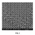
- FIG. 1illustrates an attempt by the inventors to use standard Utah Electrode Array (UEA) processing to obtain ultra-high aspect ratio electrodes.
- UAAUtah Electrode Array
- the present inventionincludes a method of fabricating an array of microelectrodes enabled to have customizable lengths and high aspect ratios.
- the array of microelectrodesmay be a three-dimensional electrical device adapted as a neural interface device or a cortical implant.
- a method of fabricating an array of microelectrodes enabled to have customizable lengthsA substantially criss-cross pattern of channels on a top surface of the work-piece substrate is formed using electrical discharge machining to form a plurality of shaped columns having tapered tips.
- the tapered tipshave a tapering profile which extends at least 50% of the length of the columns.
- the plurality of shaped columnsis etched to sharpen the tapered tips into needle tips forming the array of microelectrodes.
- FIG. 1is an SEM image of a UEA with high aspect ratio needles formed in accordance with conventional dicing and etching processing.
- FIG. 2is an illustration of a side view of rectangular channels formed by EDM in a work-piece substrate with the channels subsequently filled with a dielectric material in accordance with an embodiment.
- FIG. 3is an illustration of a side view of a work-piece substrate mounted on a conductive support substrate using removable conductive material in accordance with an embodiment.
- FIG. 4is an illustration of a side view of an array of electrodes having tapered tips formed by EDM in accordance with an embodiment.
- FIG. 5is an illustration of a side view of an array of electrodes having tapered tips etched to sharpen the electrodes in accordance with an embodiment.
- FIG. 6is a SEM perspective image of an array of electrodes formed in accordance with one embodiment.
- substantiallywhen used in reference to a quantity or amount of a material, or a specific characteristic thereof, refers to an amount that is sufficient to provide an effect that the material or characteristic was intended to provide. Therefore, “substantially free” when used in reference to a quantity or amount of a material, or a specific characteristic thereof, refers to the absence of the material or characteristic, or to the presence of the material or characteristic in an amount that is insufficient to impart a measurable effect, normally imparted by such material or characteristic.
- Numerical datamay be expressed or presented herein in a range format. It is to be understood that such a range format is used merely for convenience and brevity and thus should be interpreted flexibly to include not only the numerical values explicitly recited as the limits of the range, but also to include all the individual numerical values or sub-ranges encompassed within that range as if each numerical value and sub-range is explicitly recited. As an illustration, a numerical range of “about 0.6 mm to about 3 mm” should be interpreted to include not only the explicitly recited values of about 0.6 mm and about 3 mm, but also include individual values and sub-ranges within the indicated range.
- the term “about”means that dimensions, sizes, formulations, parameters, shapes and other quantities and characteristics are not and need not be exact, but may be approximated and/or larger or smaller, as desired, reflecting tolerances, conversion factors, rounding off, measurement error and the like and other factors known to those of skill in the art. Further, unless otherwise stated, the term “about” shall expressly include “exactly,” consistent with the discussion above regarding ranges and numerical data.
- FIG. 1illustrates an attempt by the inventors to use standard Utah Electrode Array (UEA) processing to obtain ultra-high aspect ratio electrodes.
- UAAUtah Electrode Array
- the present inventionincludes a method of fabricating an array of microelectrodes enabled to have customizable lengths and high aspect ratios.
- the array of microelectrodesmay be a three-dimensional electrical device adapted as a neural interface device or a cortical implant.
- a substrate or substrate materialmay be used to fabricate the array of microelectrodes.
- the substrateis also referred to as a work-piece substrate to differentiate the substrate from a later used optional support substrate.
- the substrate materialgenerally can be an electrically conductive material such as doped semiconductor material, metal, or combination thereof.
- Non-limiting examples of suitable materialsinclude ‘n’ or ‘p’ type silicon, tungsten, titanium, platinum, iridium, stainless steel, steel, titanium nitride, a titanium-aluminum-vanadium alloy, tungsten carbide, copper, alloys thereof, or combination thereof.
- a conductive work piece 10is first electro discharged machined to form criss-cross rectangular channels 12 a fraction of millimeter deep on one surface ( FIG. 2 ).
- a substantially criss-cross pattern of rectangular channels on the back surface of the work-piece substratecan be formed by dicing saw cuts or electrical discharge machining (EDM), although other machining techniques can be suitable (e.g. laser machining, deep reactive ion etching, etc).
- these back side cuts for the insulation linescan be performed using a dicing saw in order to prevent formation of a recast layer.
- EDMhas a tendency to form a recast layer which reduces mechanical adhesion of insulating material such as glass to the silicon.
- the dicing sawcan be a wafer cutting saw (e.g. Disco DAD685, K&S Dicing Saw Model 982-6) capable of making cuts up to 1 mm deep and up to 100 ⁇ m wide.
- a criss-cross patterncan be a first series of parallel lines or channels that are substantially perpendicular to a second series of parallel lines or channels, although skewed or other non-perpendicular cuts can be made as long as an array of columns are formed. Accordingly, the cross-sectional shape of the columns can often be square, although rectangular, triangular, hexagonal, etc. can also be formed.
- EDMincludes removing work-piece substrate material from a specified patterned area or location of the work-piece substrate using electricity. In an EDM process, material is removed by a series of rapidly recurring electric arcing discharges between an electrode (the cutting tool) and the work-piece substrate.
- any geometric shapee.g., polygon
- the channels on the back surfacecan be relatively shallow.
- the back-side channelscan generally range from about 100 ⁇ m to about 1 mm in depth.
- arrays with wider pitchcan also be formed such that even deeper channels can be formed on the back side.
- the rectangular channelscan be filled with a dielectric material to insulate the conductive electrodes or probes from each other.
- the channels created by dicing or other suitable machiningare then filled with a dielectric material (e.g. glass frit, epoxy, etc.).
- a dielectric materiale.g. glass frit, epoxy, etc.
- the dielectric materialcan be glass when silicon is used as the conductive material in the work-piece substrate, or the dielectric material can be epoxy when metal is used as the conductive material in the work-piece substrate.
- any insulating materialcan be used such as, but not limited to, glass, epoxy, adhesives, or the like.
- the next stepis to mount the work piece 10 on a conductive support substrate 14 using a temporary, highly conductive material 16 with the rectangular channels facing the support substrate ( FIG. 3 ).
- the back surface of the work-piece substratecan be mounted on a top surface of a support substrate with the conductive material sandwiched between the work-piece substrate and the support substrate.
- the support substratecan be part of the EDM machine or a conductive member associated therewith.
- the conductive material sandwiched between the work-piece substrate and the support substratecan be an epoxy, removable tape or the like.
- the back surface of the work piececan optionally be further secured or mounted on the top surface of the support substrate with an epoxy on a perimeter interface 18 of the work-piece substrate and the top surface of the support substrate.
- the perimeter interfacecan be the outer edge of the back surface of the work piece in contact with the top surface of the support substrate or the conductive material sandwiched between the work-piece substrate and the support substrate.
- the materiale.g. epoxy
- the perimeter interfacecan be the outer edge of the back surface of the work piece adjoining other sides (e.g., perpendicular sides).
- the epoxy on the perimeter interfacecan be conductive.
- the epoxycan be continuously formed on the perimeter interface or can be formed in a plurality of locations on the perimeter interface so that each location has a defined length or bead of epoxy less than the entire perimeter interface.
- the epoxy on the perimeter interfacecan optionally be discontinuous.
- other conductive supportscan be suitable, non-limiting examples can include metal (copper, aluminum etc.) stage/blocks.
- the array of ultra high aspect ratio columns/pyramidscan be machined using EDM.
- the array of tapered columns 20can be machined such that the new cuts fall on top of the dielectric material 12 to form electrically isolated array of electrodes/pyramids mechanically held together at the bottom by the dielectric material.
- the aspect ratiois limited only by the material (work piece) strength and properties.
- the advantage of this technique over the state of the artis the capability of producing pyramid like structures for what would finally be sharp needle electrodes.
- a substantially criss-cross pattern of channels on a top surface of the work-piece substratemay be formed by EDM to form a plurality of shaped columns having tapered electrodes.
- the tapered region of the columnis most often from about 50 to about 100% of the column length, although at least 90% can also be suitable.
- the tapered region, or tapering profilecan extend substantially to the base of the column as shown in FIG. 4 .
- the tips of the tapered electrodescan be of width between 20 to 50% of the base width.
- the tapered profilecan generally be a substantially linear taper from the tip to the opposite end of the taper.
- EDM cutsdo not have go all the way to the bottom, e.g. touching the glass. More specifically, EDM needs conductive material to machine such that when it hits the glass or non-conductive insulator, the wire can break in some cases. Thus, channel cuts can safely be as high as 50 ⁇ m from the bottom/glass, and the remaining material can be removed during etching.
- the aspect ratio of the columnscan range from about 1 to about 20, and in one aspect from about 1 to about 5.
- the aspect ratiocan correspond to ultra-high aspect ratio column, e.g. about 10 to about 20.
- the columnsmay be rectangular, triangular, circular, or other geometric shape (e.g., polygon) that can be formed into a column.
- Ultra high aspect columns and/or pyramidsmay be formed by EDM.
- the EDM processcan be micro-EDM such that the wire has a wire diameter in the micron range.
- the micro-EDMcan utilize a wire diameter from 30 ⁇ m to about 40 ⁇ m.
- the tapered columnscan be formed in a two stage EDM process.
- a first rough stepcan be used, followed by a second finishing step.
- the rough stepcan be accomplished by using a relatively higher pulse off time and higher electrical powers and the finishing step using a relatively lower pulse off time and lower powers.
- the cutting speed in the first stepis generally much faster than the second due to lower power parameters.
- a rough EDM stepuses a pulse off time of about 42.5 ⁇ sec, pulse on time of 4.5 ⁇ sec and a cutting speed of 1.74 mm/minute while the finishing EDM step uses a pulse off time of 12.5 ⁇ sec and pulse on time of 52.4 ⁇ sec.
- the use of two stagesallows for removal of machining debris and reduction of the recast layer from the rough step and results in a reduction in surface roughness.
- FIG. 6is an SEM of an etched high aspect ratio array formed in accordance with one embodiment of the present invention.
- the needleshave a substantially uniform taper profile from the base to the tip. These needles thus have a high mechanical strength and can be injected into tissue with minimal breakage under standard injection techniques.
- the disclosed methodallows fabrication of ultra high aspect ratio arrays for use to access deeper areas of cortex and complete coverage of nerves for recording and stimulating applications.
- the plurality of shaped columnscan be etched to sharpen the tapered tips into needle tips to form the array of microelectrodes.
- the etching of the shaped columnscan use an etchant solution.
- the etchant solutioncan be a chemical etchant, an electrochemical etchant, or combination thereof.
- suitable chemical etchants for silicon and most metal based arrayscan include HF(5% v/v)+HNO 3 (95% v/v), HF+HNO 3 +CH 3 COOH, HF+HNO 3 +CH 3 COOH+H 2 O, and for metal only H 2 SO 4 +H 2 O 2 , KOH+K 3 Fe(CN) 6 +H 2 O, etc., although others can be used.
- Non-limiting examples of suitable electrochemical etchantscan include KNO 3 , KNO 3 +H 2 O 2 , NaOH etc.
- the etchingcan be substantially static, e.g. no mixing or agitation.
- etch timecan be sufficient to achieve a substantially uniform profile needle without compromising structural integrity of the needles. For example, too short an etch time can leave the needles blocky which can reduce penetration and/or increase tissue damage upon insertion. On the other hand, excessively long etch times can result in fragile needles or complete dissolution of needles.
- etch timescan vary based on dimensions of the columns and etchant composition and conditions, as a general etch times can vary from about 1 minute to about 180 minutes (e.g.
- a sonicatorcan be used to accelerate the diffusion of ions in an etchant solution.
- an electrochemical etchingresulted in good results where shapes of the needles are affected by etching conditions. For example, a higher frequency (up to 80 Hz) produced more conical shapes and higher currents while lower frequencies ( ⁇ 5-40 Hz) tended to maintain original cross-sectional shape. Higher voltages tend to produce convex shapes under limited ion diffusion. Temperatures also play role in the surface finish and shapes of the electrodes. Higher temperatures up to 80° C. can help reduce the electrochemical etching time.
- a suitable solventsuch as acetone, xylene, isopropyl alcohol, or sequence of such solvents can be used to dissolve the conductive material or tape sandwiched between the work-piece substrate and the support substrate used to mount the work-piece substrate to the support substrate. Solvents can also be used to remove the epoxy on the perimeter interface. Acetone can used to remove the work-piece substrate from the support after the array of microelectrodes has been formed.
- the height of the shaped columns of the ultra high aspect array of microelectrodesmay be between 1.5 mm and 2 cm. In another embodiment, the height of one of the shaped columns may be between 3 mm and 10 mm with a distance between shaped column tips from 100 ⁇ m to 1 mm.
- the height of a microelectrode shaped columncan be the distance between the top point of a column and the deepest part of the trench between columns created by the EDM process and etching.
- the spacing between adjacent shaped columnsis from 50 ⁇ m to 150 ⁇ m at a base of the shaped column before etching.
- the spacing between adjacent shaped columnscan be the width of material removed at the base between two columns.
- the shaped columncan have a column length and a column width between 50 ⁇ m and 250 ⁇ m at a base of the shaped column before etching when the column shape is rectangular or square.
- the shaped columncan have a column diameter between 50 ⁇ m and 250 ⁇ m at a base of the shaped column before etching when the column shape is circular.
- the columncan be the substrate material remaining after the machining process and subsequent etching.
- the heights of the shaped columns of the ultra high aspect array of microelectrodescan vary between adjacent shaped columns or can be substantially uniform across the array. In one aspect, the height variation between two adjacent shaped columns can be up to 10% of the length of the longest electrode in an array.
- a three-dimensional array of microelectrodescan be formed using the method above.
- the three-dimensional array of microelectrodescan have a base of rigid material.
- the array of microelectrodescan have a plurality of shaped electrically conductive columns having tapered tips protruding from the base.
- Each shaped electrically conductive columncan be electrically isolated from each other at the base by a dielectric material, and a height of one of the shaped columns is between 1.5 mm and 2 cm with a distance between tips of the shaped electrically conductive columns from 100 ⁇ m to 1 mm.
- the height of one of the shaped columnscan be between 3 mm and 10 mm.
- Electrode arrayscan be further processed to form various devices and/or features as described elsewhere.
- additional processingcan include flip-chip bonding, formation of power coils, logic circuits, wireless communication, encapsulation, and the like.
- the present methodis a new technique to fabricate ultra high aspect ratio electrode array.
- Such a penetrating arraycan access deeper areas of nerves and cortex for neural signal recording and stimulation.
- the conventional technologyis only capable of producing relatively low aspect ratio electrodes.
- the disclosed methodallows fabrication of ultra high aspect ratio arrays with customizable lengths for use to access deeper areas of cortex and complete coverage of nerves for recording and stimulating applications.
Landscapes
- Health & Medical Sciences (AREA)
- Neurology (AREA)
- Neurosurgery (AREA)
- Psychology (AREA)
- Cardiology (AREA)
- Heart & Thoracic Surgery (AREA)
- Engineering & Computer Science (AREA)
- Biomedical Technology (AREA)
- Nuclear Medicine, Radiotherapy & Molecular Imaging (AREA)
- Radiology & Medical Imaging (AREA)
- Life Sciences & Earth Sciences (AREA)
- Animal Behavior & Ethology (AREA)
- General Health & Medical Sciences (AREA)
- Public Health (AREA)
- Veterinary Medicine (AREA)
- Electrical Discharge Machining, Electrochemical Machining, And Combined Machining (AREA)
- Electrotherapy Devices (AREA)
Abstract
Description
Claims (16)
Priority Applications (1)
| Application Number | Priority Date | Filing Date | Title |
|---|---|---|---|
| US12/996,356US8886279B2 (en) | 2008-06-03 | 2009-06-03 | High aspect ratio microelectrode arrays enabled to have customizable lengths and methods of making the same |
Applications Claiming Priority (3)
| Application Number | Priority Date | Filing Date | Title |
|---|---|---|---|
| US5831008P | 2008-06-03 | 2008-06-03 | |
| PCT/US2009/046150WO2009149197A2 (en) | 2008-06-03 | 2009-06-03 | High aspect ratio microelectrode arrays enabled to have customizable lengths and methods of making the same |
| US12/996,356US8886279B2 (en) | 2008-06-03 | 2009-06-03 | High aspect ratio microelectrode arrays enabled to have customizable lengths and methods of making the same |
Publications (2)
| Publication Number | Publication Date |
|---|---|
| US20120138335A1 US20120138335A1 (en) | 2012-06-07 |
| US8886279B2true US8886279B2 (en) | 2014-11-11 |
Family
ID=41398847
Family Applications (1)
| Application Number | Title | Priority Date | Filing Date |
|---|---|---|---|
| US12/996,356Active - Reinstated2030-07-21US8886279B2 (en) | 2008-06-03 | 2009-06-03 | High aspect ratio microelectrode arrays enabled to have customizable lengths and methods of making the same |
Country Status (2)
| Country | Link |
|---|---|
| US (1) | US8886279B2 (en) |
| WO (1) | WO2009149197A2 (en) |
Cited By (10)
| Publication number | Priority date | Publication date | Assignee | Title |
|---|---|---|---|---|
| US20130066182A1 (en)* | 2011-09-14 | 2013-03-14 | Neuronexus Technologies, Inc. | Methods for Forming an Electrode Device with Reduced Impedance |
| US20140259652A1 (en)* | 2013-03-14 | 2014-09-18 | Sano Intelligence, Inc. | On-body microsensor for biomonitoring |
| US10549099B2 (en) | 2016-04-29 | 2020-02-04 | University Of Utah Research Foundation | Electronic peripheral nerve stimulation |
| US10595754B2 (en) | 2014-03-13 | 2020-03-24 | Sano Intelligence, Inc. | System for monitoring body chemistry |
| US10820860B2 (en) | 2013-03-14 | 2020-11-03 | One Drop Biosensor Technologies, Llc | On-body microsensor for biomonitoring |
| US11272866B2 (en) | 2014-03-13 | 2022-03-15 | One Drop Biosensor Technologies, Llc | Wearable microneedle patch |
| USD988882S1 (en) | 2021-04-21 | 2023-06-13 | Informed Data Systems Inc. | Sensor assembly |
| US20250083243A1 (en)* | 2022-07-25 | 2025-03-13 | Wuhan Neuracom Technology Development Co., Ltd. | Reverse soldering connection structure of microneedle and wiring and preparation process therefor |
| USD1076079S1 (en) | 2021-04-21 | 2025-05-20 | One Health Biosensing Inc. | Applicator assembly |
| USD1086030S1 (en) | 2021-04-21 | 2025-07-29 | One Health Biosensing Inc. | Charging station |
Families Citing this family (17)
| Publication number | Priority date | Publication date | Assignee | Title |
|---|---|---|---|---|
| EP2174118A4 (en)* | 2007-02-01 | 2015-06-24 | Ls Biopath Inc | Optical system for identification and characterization of abnormal tissue and cells |
| WO2008095108A1 (en)* | 2007-02-01 | 2008-08-07 | Ls Biopath, Inc. | Electrical systems for detection and characterization of abnormal tissue and cells |
| FR2933621B1 (en)* | 2008-07-11 | 2010-09-10 | Commissariat Energie Atomique | IMPLANTABLE PROBE |
| EA022775B1 (en)* | 2010-08-25 | 2016-02-29 | Неуронано Аб | Displacement resistant microelectrode, microelectrode bundle and microelectrode array for implantation into soft tissue of a person or animal |
| KR20120046554A (en)* | 2010-11-02 | 2012-05-10 | 연세대학교 산학협력단 | Sensor for detecting cancer tissue and manufacturing method of the same |
| EP4309639A3 (en)* | 2011-06-14 | 2024-02-14 | ViOL Co., Ltd. | Apparatus and method for improving skin using a ra-effect or ra plus-effect |
| US9238093B2 (en) | 2011-11-21 | 2016-01-19 | Medtronic, Inc | Surface improvement on electric discharge machined titanium alloy miniature parts for implantable medical device |
| NL2009945C2 (en)* | 2012-12-10 | 2014-06-11 | Univ Leiden | Process and device for minimally invasive deep tissue probing. |
| WO2014092566A1 (en)* | 2012-12-10 | 2014-06-19 | Universiteit Leiden | Process and device for minimally invasive deep tissue probing |
| WO2015143443A1 (en) | 2014-03-21 | 2015-09-24 | University Of Utah Research Foundation | Multi-site electrode arrays and methods of making the same |
| KR101585197B1 (en) | 2014-04-10 | 2016-01-14 | 재단법인대구경북과학기술원 | Nano-Micro probe and manufacturing method of the same |
| CN104398258B (en)* | 2014-11-03 | 2016-05-25 | 中国科学院深圳先进技术研究院 | 3D fibril electrode array fixture and 3D fibril electrode array method of cutting out |
| US11547849B2 (en) | 2017-06-07 | 2023-01-10 | Neuronexus Technologies, Inc. | Systems and methods for ruggedized penetrating medical electrode arrays |
| EP3527254B1 (en)* | 2018-02-14 | 2020-08-05 | Dyconex AG | Implantable multielectrode array |
| US11109787B2 (en)* | 2018-05-21 | 2021-09-07 | Vine Medical LLC | Multi-tip probe for obtaining bioelectrical measurements |
| CN109030600B (en)* | 2018-07-30 | 2023-05-23 | 浙江大学 | Sandable microelectrode array and its packaging and use method |
| CN112237682B (en)* | 2019-07-17 | 2024-09-17 | 杭州暖芯迦电子科技有限公司 | Miniature high-density array free-form surface electrode and manufacturing method thereof |
Citations (62)
| Publication number | Priority date | Publication date | Assignee | Title |
|---|---|---|---|---|
| US4685466A (en) | 1985-01-29 | 1987-08-11 | Rau Guenter | Measuring sensor for the non-invasive detection of electro-physiological quantities |
| US4837049A (en) | 1986-06-17 | 1989-06-06 | Alfred E. Mann Foundation For Scientific Research | Method of making an electrode array |
| US4969468A (en)* | 1986-06-17 | 1990-11-13 | Alfred E. Mann Foundation For Scientific Research | Electrode array for use in connection with a living body and method of manufacture |
| US5215088A (en) | 1989-11-07 | 1993-06-01 | The University Of Utah | Three-dimensional electrode device |
| US5286944A (en) | 1992-03-25 | 1994-02-15 | Panasonic Technologies, Inc. | Method of manufacturing a multiple microelectrode assembly |
| US5388577A (en)* | 1990-06-08 | 1995-02-14 | Boston University | Electrode array microchip |
| US5457041A (en) | 1994-03-25 | 1995-10-10 | Science Applications International Corporation | Needle array and method of introducing biological substances into living cells using the needle array |
| US5472592A (en) | 1994-07-19 | 1995-12-05 | American Plating Systems | Electrolytic plating apparatus and method |
| US5591139A (en)* | 1994-06-06 | 1997-01-07 | The Regents Of The University Of California | IC-processed microneedles |
| US5656414A (en) | 1993-04-23 | 1997-08-12 | Fujitsu Limited | Methods of forming tall, high-aspect ratio vias and trenches in photo-imageable materials, photoresist materials, and the like |
| US5689603A (en) | 1993-07-07 | 1997-11-18 | Huth; Gerald C. | Optically interactive nanostructure |
| US5838715A (en) | 1996-06-20 | 1998-11-17 | Hewlett-Packard Company | High intensity single-mode VCSELs |
| US5895562A (en) | 1997-06-19 | 1999-04-20 | Advanced Micro Devices, Inc. | Gas shielding during plating |
| US6091975A (en)* | 1998-04-01 | 2000-07-18 | Alza Corporation | Minimally invasive detecting device |
| US6285446B1 (en) | 1997-05-19 | 2001-09-04 | Sensornet Limited | Distributed sensing system |
| US6334856B1 (en) | 1998-06-10 | 2002-01-01 | Georgia Tech Research Corporation | Microneedle devices and methods of manufacture and use thereof |
| US6406638B1 (en) | 2000-01-06 | 2002-06-18 | The Regents Of The University Of California | Method of forming vertical, hollow needles within a semiconductor substrate, and needles formed thereby |
| US20020082543A1 (en) | 2000-12-14 | 2002-06-27 | Jung-Hwan Park | Microneedle devices and production thereof |
| US6511463B1 (en) | 1999-11-18 | 2003-01-28 | Jds Uniphase Corporation | Methods of fabricating microneedle arrays using sacrificial molds |
| US6551849B1 (en) | 1999-11-02 | 2003-04-22 | Christopher J. Kenney | Method for fabricating arrays of micro-needles |
| US6622035B1 (en)* | 2000-01-21 | 2003-09-16 | Instrumentarium Corp. | Electrode for measurement of weak bioelectrical signals |
| US20030208138A1 (en) | 2001-07-09 | 2003-11-06 | Lorin Olson | Micro-needles and methods of manufacture and use thereof |
| US6702950B2 (en) | 1999-06-16 | 2004-03-09 | James E. Moon | Method for fabricating LC device using latent masking and delayed LOCOS techniques |
| US20040048419A1 (en) | 2001-11-30 | 2004-03-11 | Masahiko Kitamura | Production method for semiconductor chip |
| US20040082875A1 (en)* | 2002-10-24 | 2004-04-29 | Brown University Research Foundation | Microstructured arrays for cortex interaction and related methods of manufacture and use |
| US6730444B2 (en) | 2001-06-05 | 2004-05-04 | Micron Technology, Inc. | Needle comb reticle pattern for critical dimension and registration measurements using a registration tool and methods for using same |
| US6743211B1 (en) | 1999-11-23 | 2004-06-01 | Georgia Tech Research Corporation | Devices and methods for enhanced microneedle penetration of biological barriers |
| US6782283B2 (en)* | 2001-09-07 | 2004-08-24 | Robert N. Schmidt | Dry penetrating recording device |
| US6815360B1 (en) | 1998-07-22 | 2004-11-09 | Qinetiq Limited | Silicon micro-machined projection with duct |
| US20040267205A1 (en) | 2001-08-14 | 2004-12-30 | Goran Stemme | Micro needles and method of manufacture thereof |
| US20050011858A1 (en) | 2003-07-16 | 2005-01-20 | Industrial Technology Research Institute | Method for fabricating a hollow micro-needle array |
| US6896850B2 (en) | 2001-03-26 | 2005-05-24 | Kumetrix, Inc. | Silicon nitride window for microsampling device and method of construction |
| US20050171480A1 (en) | 2003-11-21 | 2005-08-04 | The Regents Of The University Of California | Method and/or apparatus for puncturing a surface for extraction, in situ analysis, and/or substance delivery using microneedles |
| WO2005072630A1 (en) | 2004-01-30 | 2005-08-11 | Isis Innovation Limited | Device for delivery of bioactive materials and other stimuli |
| US6980282B2 (en) | 2002-12-11 | 2005-12-27 | Molecular Imprints, Inc. | Method for modulating shapes of substrates |
| US20060055090A1 (en) | 2003-01-16 | 2006-03-16 | Lee Seung-Seob | Method for manufacturing of polymer micro needle array with liga process |
| US7027874B1 (en)* | 2000-11-16 | 2006-04-11 | Polyvalor S.E.C. | Body electronic implant and artificial vision system thereof |
| US20060110100A1 (en) | 2003-01-24 | 2006-05-25 | Blauvelt Henry A | Etched-facet semiconductor optical component with integrated end-coupled waveguide and methods of fabrication and use thereof |
| WO2006055799A1 (en) | 2004-11-18 | 2006-05-26 | 3M Innovative Properties Company | Masking method for coating a microneedle array |
| US20060127307A1 (en) | 2003-01-31 | 2006-06-15 | Canham Leight T | Devices and compositions containing boron and silicon for use in neutron capture therapy |
| US20060135862A1 (en)* | 2003-06-12 | 2006-06-22 | Tootle John S | Multielectrode array and system for recording and analyzing data or for stimulating tissue |
| US20060173259A1 (en)* | 2004-10-04 | 2006-08-03 | Flaherty J C | Biological interface system |
| US7118942B1 (en) | 2000-09-27 | 2006-10-10 | Li Chou H | Method of making atomic integrated circuit device |
| US20070067007A1 (en)* | 2005-05-25 | 2007-03-22 | Alfred E. Mann Foundation For Scientific Research | Hermetically sealed three-dimensional electrode array |
| US7240416B2 (en) | 2001-05-07 | 2007-07-10 | Cochlear Limited | Process for manufacturing electrically conductive components |
| US20070161964A1 (en) | 2006-01-10 | 2007-07-12 | Yuzhakov Vadim V | Microneedle array, patch, and applicator for transdermal drug delivery |
| US7310543B2 (en)* | 2001-03-26 | 2007-12-18 | Kumetrix, Inc. | Silicon microprobe with integrated biosensor |
| US20080125743A1 (en) | 2006-11-28 | 2008-05-29 | Yuzhakov Vadim V | Tissue Conforming Microneedle Array and Patch For Transdermal Drug Delivery or Biological Fluid Collection |
| US20080138581A1 (en) | 2006-07-17 | 2008-06-12 | Rajmohan Bhandari | Masking high-aspect aspect ratio structures |
| US20080138582A1 (en) | 2006-07-17 | 2008-06-12 | Rajmohan Bhandari | Water-scale needle array |
| US20080138583A1 (en) | 2006-07-17 | 2008-06-12 | Rajmohan Bhandari | Micro-needle arrays having non-planar tips and methods of manufacture thereof |
| US20080249391A1 (en)* | 2006-07-18 | 2008-10-09 | Drexel University | Chronic in-vivo neurotransmitter sensor |
| US20080262416A1 (en) | 2005-11-18 | 2008-10-23 | Duan Daniel C | Microneedle Arrays and Methods of Preparing Same |
| US20080275400A1 (en) | 2005-12-23 | 2008-11-06 | Ferguson Dennis E | Manufacturing Microneedle Arrays |
| US20090011158A1 (en) | 2007-03-18 | 2009-01-08 | Nanopass Technologies Ltd. | Microneedle structures and corresponding production methods employing a backside wet etch |
| US20090099534A1 (en) | 2006-07-12 | 2009-04-16 | University Of Utah Research Foundation | 3D fabrication of needle tip geometry and knife blade |
| US20090283425A1 (en)* | 2008-04-02 | 2009-11-19 | University Of Utah Research Foundation | Microelectrode Array System With Integrated Reference Microelectrodes To Reduce Detected Electrical Noise And Improve Selectivity Of Activation |
| US20090301994A1 (en) | 2008-05-12 | 2009-12-10 | Rajmohan Bhandari | Methods for Wafer Scale Processing of Needle Array Devices |
| US20100029148A1 (en)* | 2008-07-29 | 2010-02-04 | Gayatri Eadara Perlin | Compact multilevel electrical integration of microsystems |
| US20100041972A1 (en)* | 2006-07-07 | 2010-02-18 | Lectus Therapeutics Limited | Apparatus and methods |
| US7712198B2 (en) | 2004-07-16 | 2010-05-11 | Industrial Technology Research Institute | Microneedle array device and its fabrication method |
| US7991475B1 (en)* | 2005-06-08 | 2011-08-02 | The Regents Of The University Of California | High density micromachined electrode arrays useable for auditory nerve implants and related methods |
- 2009
- 2009-06-03USUS12/996,356patent/US8886279B2/enactiveActive - Reinstated
- 2009-06-03WOPCT/US2009/046150patent/WO2009149197A2/enactiveApplication Filing
Patent Citations (68)
| Publication number | Priority date | Publication date | Assignee | Title |
|---|---|---|---|---|
| US4685466A (en) | 1985-01-29 | 1987-08-11 | Rau Guenter | Measuring sensor for the non-invasive detection of electro-physiological quantities |
| US4837049A (en) | 1986-06-17 | 1989-06-06 | Alfred E. Mann Foundation For Scientific Research | Method of making an electrode array |
| US4969468A (en)* | 1986-06-17 | 1990-11-13 | Alfred E. Mann Foundation For Scientific Research | Electrode array for use in connection with a living body and method of manufacture |
| US5215088A (en) | 1989-11-07 | 1993-06-01 | The University Of Utah | Three-dimensional electrode device |
| US5388577A (en)* | 1990-06-08 | 1995-02-14 | Boston University | Electrode array microchip |
| US5286944A (en) | 1992-03-25 | 1994-02-15 | Panasonic Technologies, Inc. | Method of manufacturing a multiple microelectrode assembly |
| US5656414A (en) | 1993-04-23 | 1997-08-12 | Fujitsu Limited | Methods of forming tall, high-aspect ratio vias and trenches in photo-imageable materials, photoresist materials, and the like |
| US5689603A (en) | 1993-07-07 | 1997-11-18 | Huth; Gerald C. | Optically interactive nanostructure |
| US5457041A (en) | 1994-03-25 | 1995-10-10 | Science Applications International Corporation | Needle array and method of introducing biological substances into living cells using the needle array |
| US5591139A (en)* | 1994-06-06 | 1997-01-07 | The Regents Of The University Of California | IC-processed microneedles |
| US5472592A (en) | 1994-07-19 | 1995-12-05 | American Plating Systems | Electrolytic plating apparatus and method |
| US5838715A (en) | 1996-06-20 | 1998-11-17 | Hewlett-Packard Company | High intensity single-mode VCSELs |
| US6285446B1 (en) | 1997-05-19 | 2001-09-04 | Sensornet Limited | Distributed sensing system |
| US5895562A (en) | 1997-06-19 | 1999-04-20 | Advanced Micro Devices, Inc. | Gas shielding during plating |
| US6091975A (en)* | 1998-04-01 | 2000-07-18 | Alza Corporation | Minimally invasive detecting device |
| US6334856B1 (en) | 1998-06-10 | 2002-01-01 | Georgia Tech Research Corporation | Microneedle devices and methods of manufacture and use thereof |
| US6815360B1 (en) | 1998-07-22 | 2004-11-09 | Qinetiq Limited | Silicon micro-machined projection with duct |
| US6702950B2 (en) | 1999-06-16 | 2004-03-09 | James E. Moon | Method for fabricating LC device using latent masking and delayed LOCOS techniques |
| US6551849B1 (en) | 1999-11-02 | 2003-04-22 | Christopher J. Kenney | Method for fabricating arrays of micro-needles |
| US7332197B2 (en) | 1999-11-18 | 2008-02-19 | Memscap S.A. | Methods of fabricating microneedle arrays using sacrificial molds, and microneedle arrays fabricated thereby |
| US6511463B1 (en) | 1999-11-18 | 2003-01-28 | Jds Uniphase Corporation | Methods of fabricating microneedle arrays using sacrificial molds |
| US6743211B1 (en) | 1999-11-23 | 2004-06-01 | Georgia Tech Research Corporation | Devices and methods for enhanced microneedle penetration of biological barriers |
| US20050137531A1 (en) | 1999-11-23 | 2005-06-23 | Prausnitz Mark R. | Devices and methods for enhanced microneedle penetration of biological barriers |
| US6406638B1 (en) | 2000-01-06 | 2002-06-18 | The Regents Of The University Of California | Method of forming vertical, hollow needles within a semiconductor substrate, and needles formed thereby |
| US6622035B1 (en)* | 2000-01-21 | 2003-09-16 | Instrumentarium Corp. | Electrode for measurement of weak bioelectrical signals |
| US7118942B1 (en) | 2000-09-27 | 2006-10-10 | Li Chou H | Method of making atomic integrated circuit device |
| US7027874B1 (en)* | 2000-11-16 | 2006-04-11 | Polyvalor S.E.C. | Body electronic implant and artificial vision system thereof |
| US20020082543A1 (en) | 2000-12-14 | 2002-06-27 | Jung-Hwan Park | Microneedle devices and production thereof |
| US7310543B2 (en)* | 2001-03-26 | 2007-12-18 | Kumetrix, Inc. | Silicon microprobe with integrated biosensor |
| US6896850B2 (en) | 2001-03-26 | 2005-05-24 | Kumetrix, Inc. | Silicon nitride window for microsampling device and method of construction |
| US7240416B2 (en) | 2001-05-07 | 2007-07-10 | Cochlear Limited | Process for manufacturing electrically conductive components |
| US6730444B2 (en) | 2001-06-05 | 2004-05-04 | Micron Technology, Inc. | Needle comb reticle pattern for critical dimension and registration measurements using a registration tool and methods for using same |
| US20030208138A1 (en) | 2001-07-09 | 2003-11-06 | Lorin Olson | Micro-needles and methods of manufacture and use thereof |
| US20040267205A1 (en) | 2001-08-14 | 2004-12-30 | Goran Stemme | Micro needles and method of manufacture thereof |
| US6782283B2 (en)* | 2001-09-07 | 2004-08-24 | Robert N. Schmidt | Dry penetrating recording device |
| US20040048419A1 (en) | 2001-11-30 | 2004-03-11 | Masahiko Kitamura | Production method for semiconductor chip |
| US7212851B2 (en) | 2002-10-24 | 2007-05-01 | Brown University Research Foundation | Microstructured arrays for cortex interaction and related methods of manufacture and use |
| US20040082875A1 (en)* | 2002-10-24 | 2004-04-29 | Brown University Research Foundation | Microstructured arrays for cortex interaction and related methods of manufacture and use |
| US6980282B2 (en) | 2002-12-11 | 2005-12-27 | Molecular Imprints, Inc. | Method for modulating shapes of substrates |
| US20060055090A1 (en) | 2003-01-16 | 2006-03-16 | Lee Seung-Seob | Method for manufacturing of polymer micro needle array with liga process |
| US20060110100A1 (en) | 2003-01-24 | 2006-05-25 | Blauvelt Henry A | Etched-facet semiconductor optical component with integrated end-coupled waveguide and methods of fabrication and use thereof |
| US20060127307A1 (en) | 2003-01-31 | 2006-06-15 | Canham Leight T | Devices and compositions containing boron and silicon for use in neutron capture therapy |
| US20060135862A1 (en)* | 2003-06-12 | 2006-06-22 | Tootle John S | Multielectrode array and system for recording and analyzing data or for stimulating tissue |
| US20050011858A1 (en) | 2003-07-16 | 2005-01-20 | Industrial Technology Research Institute | Method for fabricating a hollow micro-needle array |
| US20050171480A1 (en) | 2003-11-21 | 2005-08-04 | The Regents Of The University Of California | Method and/or apparatus for puncturing a surface for extraction, in situ analysis, and/or substance delivery using microneedles |
| WO2005072630A1 (en) | 2004-01-30 | 2005-08-11 | Isis Innovation Limited | Device for delivery of bioactive materials and other stimuli |
| US7712198B2 (en) | 2004-07-16 | 2010-05-11 | Industrial Technology Research Institute | Microneedle array device and its fabrication method |
| US20060173259A1 (en)* | 2004-10-04 | 2006-08-03 | Flaherty J C | Biological interface system |
| WO2006055799A1 (en) | 2004-11-18 | 2006-05-26 | 3M Innovative Properties Company | Masking method for coating a microneedle array |
| US20080102192A1 (en) | 2004-11-18 | 2008-05-01 | Johnson Peter R | Masking Method for Coating a Microneedle Array |
| US20070067007A1 (en)* | 2005-05-25 | 2007-03-22 | Alfred E. Mann Foundation For Scientific Research | Hermetically sealed three-dimensional electrode array |
| US7991475B1 (en)* | 2005-06-08 | 2011-08-02 | The Regents Of The University Of California | High density micromachined electrode arrays useable for auditory nerve implants and related methods |
| US20080262416A1 (en) | 2005-11-18 | 2008-10-23 | Duan Daniel C | Microneedle Arrays and Methods of Preparing Same |
| US20080275400A1 (en) | 2005-12-23 | 2008-11-06 | Ferguson Dennis E | Manufacturing Microneedle Arrays |
| US20070161964A1 (en) | 2006-01-10 | 2007-07-12 | Yuzhakov Vadim V | Microneedle array, patch, and applicator for transdermal drug delivery |
| US20100041972A1 (en)* | 2006-07-07 | 2010-02-18 | Lectus Therapeutics Limited | Apparatus and methods |
| US20090099534A1 (en) | 2006-07-12 | 2009-04-16 | University Of Utah Research Foundation | 3D fabrication of needle tip geometry and knife blade |
| US20080138583A1 (en) | 2006-07-17 | 2008-06-12 | Rajmohan Bhandari | Micro-needle arrays having non-planar tips and methods of manufacture thereof |
| US20080138582A1 (en) | 2006-07-17 | 2008-06-12 | Rajmohan Bhandari | Water-scale needle array |
| US20080138581A1 (en) | 2006-07-17 | 2008-06-12 | Rajmohan Bhandari | Masking high-aspect aspect ratio structures |
| US20120132613A1 (en) | 2006-07-17 | 2012-05-31 | Rajmohan Bhandari | Wafer-scale needle array |
| US7951300B2 (en) | 2006-07-17 | 2011-05-31 | University Of Utah Research Foundation | Water-scale needle array |
| US20080249391A1 (en)* | 2006-07-18 | 2008-10-09 | Drexel University | Chronic in-vivo neurotransmitter sensor |
| US20080125743A1 (en) | 2006-11-28 | 2008-05-29 | Yuzhakov Vadim V | Tissue Conforming Microneedle Array and Patch For Transdermal Drug Delivery or Biological Fluid Collection |
| US20090011158A1 (en) | 2007-03-18 | 2009-01-08 | Nanopass Technologies Ltd. | Microneedle structures and corresponding production methods employing a backside wet etch |
| US20090283425A1 (en)* | 2008-04-02 | 2009-11-19 | University Of Utah Research Foundation | Microelectrode Array System With Integrated Reference Microelectrodes To Reduce Detected Electrical Noise And Improve Selectivity Of Activation |
| US20090301994A1 (en) | 2008-05-12 | 2009-12-10 | Rajmohan Bhandari | Methods for Wafer Scale Processing of Needle Array Devices |
| US20100029148A1 (en)* | 2008-07-29 | 2010-02-04 | Gayatri Eadara Perlin | Compact multilevel electrical integration of microsystems |
Non-Patent Citations (15)
| Title |
|---|
| Bhandari et al; A Novel Method of Fabrication Convoluted Shaped Electrode Arrays for Neural and Retinal Prostheses; Sensors and Actuators A; Nov. 4, 2007; pp. 123-130; vol. 145-146. |
| Branner et al; Long Term Stimulation and Recording with a Penetration Microelectrode Array in Cat Sciatic Nerve; IEEE Transactions on Biomedical Engineering; vol. 51, No. 1; Jan. 2004. |
| Campbell et al.; A Silicon-Based, Three Dimensional Neural Interface: Manufacturing Process for an Intracortical Electrode Array; IEEE; Aug. 1991; pp. 758-768; vol. 38, No. 8. |
| Clark et al.; DARPA Revolutionizing Prosthetics 2009; Making It Work: Animal Physiology & Device Testing; Dept. of Bioengineering University of Utah Jun. 28, 2007; 5 pgs. |
| Dhillon et al.; Residual Function in Peripheral Nerve Stumps of Amputees: Implications for Neural Control of Artificial Limbs; The Journal of Hand Surgery; 2004; pp. 605-615. |
| Fofonoff et al.; A Highly Flexible Manufacturing Technique for Microelectrode Array Fabrication in: [Engineering in Medicine and Biology, 2002; 24th Annual Conference and the Annual Fall meeting of the Biomedical Engineering Society] EMBS/BMES Conference; 2002; pp. 2107-2108. |
| Fofonoff et al.; Assembly-Ready Brain Microelectrode Array's in: Engineering in Medicine and Biology Society, Proceedings of the 25th Annual International Conference of the IEEE, 2003, pp. 1937-1940. |
| Jones et al.; A Glass/Silicon Composite Intracortical Electrode Array; Annals of Biomedical Engineering; 1992; pp. 423-437; vol. 20. |
| Rakwal et al; Fabrication of Compliant High Aspect Ratio Silicon Microelectrode Arrays Using Micro-Wire Electrical Discharge Machining; Microsyst Technol; 2009; pp. 789-797; vol. 15. |
| Tajadod et al.; Electophoretic Photoresist Application for High Topography Wafer Surfaces; International Conference on Compound Semiconductor Mfg; 2003; 4 pgs. |
| Tathireddy et al; Fabrication of 3-Dimensional Silicon Microelectrode Arrays Using Micro Electro Discharge Machining for Neural Applications; Proc. Transducer'09, 15th Int. Conf. on Solid-State Sensors, Actuators and Microsystems, Denver, CO, Jun. 21-25, 2009, pp. 1206-1209. |
| Tathireddy et al; Towards High Aspect Ratio Tungsten Micro Electrode Array for Neural Recording and Stimulation Applications; 13th Annual International Function Electrical Stimulation (FES) Society Conference, Freiburg, Germany, Sep. 21-25, 2008. |
| Tsung-Kuan et al.; Fabrication of Out-of-Plane Curved Surfaces in Si by Utilizing Rie Lag; IEEE; 2002; pp. 145-148. |
| U.S. Appl. No. 11/807,766, filed May 29, 2007, Rajmohan Bhandari; office action dated Feb. 19, 2013. |
| U.S. Appl. No. 12/464,691, filed May 12, 2009, Rajmohan Bhandari; office action dated Feb. 7, 2013. |
Cited By (32)
| Publication number | Priority date | Publication date | Assignee | Title |
|---|---|---|---|---|
| US20130066182A1 (en)* | 2011-09-14 | 2013-03-14 | Neuronexus Technologies, Inc. | Methods for Forming an Electrode Device with Reduced Impedance |
| US10052476B2 (en) | 2011-09-14 | 2018-08-21 | Neuronexus Technologies, Inc. | Methods for forming an electrode device with reduced impedance |
| US11096614B2 (en) | 2011-09-14 | 2021-08-24 | Neuronexus Technologies, Inc. | Methods for forming an electrode device with reduced impedance |
| US9192757B2 (en)* | 2011-09-14 | 2015-11-24 | Greatbatch Ltd. | Methods for forming an electrode device with reduced impedance |
| US10173042B2 (en) | 2013-03-14 | 2019-01-08 | Sano Intelligence, Inc. | Method of manufacturing a sensor for sensing analytes |
| US11123532B2 (en)* | 2013-03-14 | 2021-09-21 | One Drop Biosensor Technologies, Llc | On-body microsensor for biomonitoring |
| US11903738B2 (en) | 2013-03-14 | 2024-02-20 | One Drop Biosensor Technologies, Llc | On-body microsensor for biomonitoring |
| US10549080B2 (en) | 2013-03-14 | 2020-02-04 | Sano Intelligence, Inc. | On-body microsensor for biomonitoring |
| US20140259652A1 (en)* | 2013-03-14 | 2014-09-18 | Sano Intelligence, Inc. | On-body microsensor for biomonitoring |
| US9182368B2 (en)* | 2013-03-14 | 2015-11-10 | Sano Intelligence, Inc. | Method of manufacturing a sensor for sensing analytes |
| US10820860B2 (en) | 2013-03-14 | 2020-11-03 | One Drop Biosensor Technologies, Llc | On-body microsensor for biomonitoring |
| US11819650B2 (en) | 2013-03-14 | 2023-11-21 | One Drop Biosensor Technologies, Llc | Method of manufacturing multi-analyte microsensor with microneedles |
| US11896793B2 (en) | 2013-03-14 | 2024-02-13 | One Drop Biosensor Technologies, Llc | On-body microsensor for biomonitoring |
| US11197985B2 (en)* | 2013-03-14 | 2021-12-14 | One Drop Biosensor Technologies, Llc | Method of manufacturing multi-analyte microsensor with microneedles |
| US20220054813A1 (en)* | 2013-03-14 | 2022-02-24 | One Drop Biosensor Technologies, Llc | On-body microsensor for biomonitoring |
| US11272885B2 (en) | 2013-03-14 | 2022-03-15 | One Drop Biosensor Technologies, Llc | Wearable multi-analyte microsensor |
| US11896792B2 (en) | 2013-03-14 | 2024-02-13 | One Drop Biosensor Technologies, Llc | On-body microsensor for biomonitoring |
| US11865289B2 (en)* | 2013-03-14 | 2024-01-09 | One Drop Biosensor Technologies, Llc | On-body microsensor for biomonitoring |
| US10595754B2 (en) | 2014-03-13 | 2020-03-24 | Sano Intelligence, Inc. | System for monitoring body chemistry |
| US12303260B2 (en) | 2014-03-13 | 2025-05-20 | One Health Biosensing Inc. | System for monitoring body chemistry |
| US11517222B2 (en) | 2014-03-13 | 2022-12-06 | One Drop Biosensor Technologies, Llc | Biomonitoring systems and methods of loading and releasing the same |
| US11357430B2 (en) | 2014-03-13 | 2022-06-14 | One Drop Biosensor Technologies, Llc | Biomonitoring systems and methods of loading and releasing the same |
| US11291390B2 (en) | 2014-03-13 | 2022-04-05 | One Drop Biosensor Technologies, Llc | Wearable microneedle patch |
| US11272866B2 (en) | 2014-03-13 | 2022-03-15 | One Drop Biosensor Technologies, Llc | Wearable microneedle patch |
| US11172851B2 (en) | 2014-03-13 | 2021-11-16 | One Drop Biosensor Technologies, Llc | System for monitoring body chemistry |
| US10549099B2 (en) | 2016-04-29 | 2020-02-04 | University Of Utah Research Foundation | Electronic peripheral nerve stimulation |
| USD1038788S1 (en) | 2021-04-21 | 2024-08-13 | One Health Biosensing Inc. | Sensor assembly |
| USD988882S1 (en) | 2021-04-21 | 2023-06-13 | Informed Data Systems Inc. | Sensor assembly |
| USD1076079S1 (en) | 2021-04-21 | 2025-05-20 | One Health Biosensing Inc. | Applicator assembly |
| USD1086030S1 (en) | 2021-04-21 | 2025-07-29 | One Health Biosensing Inc. | Charging station |
| US20250083243A1 (en)* | 2022-07-25 | 2025-03-13 | Wuhan Neuracom Technology Development Co., Ltd. | Reverse soldering connection structure of microneedle and wiring and preparation process therefor |
| US12434315B2 (en)* | 2022-07-25 | 2025-10-07 | Wuhan Neuracom Technology Development Co., Ltd. | Reverse soldering connection structure of microneedle and wiring and preparation process therefor |
Also Published As
| Publication number | Publication date |
|---|---|
| WO2009149197A3 (en) | 2010-03-11 |
| US20120138335A1 (en) | 2012-06-07 |
| WO2009149197A2 (en) | 2009-12-10 |
Similar Documents
| Publication | Publication Date | Title |
|---|---|---|
| US8886279B2 (en) | High aspect ratio microelectrode arrays enabled to have customizable lengths and methods of making the same | |
| Arab et al. | Effect of tool electrode roughness on the geometric characteristics of through-holes formed by ECDM | |
| US7951300B2 (en) | Water-scale needle array | |
| US8865288B2 (en) | Micro-needle arrays having non-planar tips and methods of manufacture thereof | |
| Kannojia et al. | Fabrication and characterization of through-glass vias by the ECDM process | |
| US20090301994A1 (en) | Methods for Wafer Scale Processing of Needle Array Devices | |
| US5559389A (en) | Electron-emitting devices having variously constituted electron-emissive elements, including cones or pedestals | |
| EP0666595B1 (en) | Method of manufacture of a cubic integrated circuit structure | |
| DE10338291B4 (en) | A method of manufacturing a semiconductor device with penetrating electrodes by anodic oxidation | |
| CN100406898C (en) | Probe array and its manufacturing method | |
| US4096619A (en) | Semiconductor scribing method | |
| US20100036470A1 (en) | Laser-Based Fabrication of Implantable Stimulation Electrodes | |
| US20200056299A1 (en) | Patterned microwire bundles and methods of producing the same | |
| Leber et al. | Different methods to alter surface morphology of high aspect ratio structures | |
| DE102019204974B4 (en) | WAFER PROCESSING METHODS | |
| JP2014227556A (en) | Processing method of substrate, and template | |
| Tathireddy et al. | Fabrication of 3-dimensional silicon microelectrode arrays using micro electro discharge machining for neural applications | |
| DE102006043163B4 (en) | Semiconductor circuitry | |
| DE10055712A1 (en) | Production of trench capacitors in a p-doped silicon layer used for DRAMs and ferroelectric semiconductor storage devices comprises using electrodes and a capacitor dielectric | |
| Peixoto et al. | Invasive neural electrodes structure fabrication based on aluminum wafers | |
| Bhandari et al. | Wafer-scale processed, low impedance, neural arrays with varying length microelectrodes | |
| Xu et al. | Anodic-Bonding-Assisted Silicon Microelectrode Array For Neural Applications | |
| DE102006031407A1 (en) | Silicon semiconductor wafer thinning for production of power semiconductor component, involves thinning polished wafer until semiconductor wafer with preset wafer thickness of less than specific micrometer is obtained | |
| TWI549653B (en) | Probe array and manufacturing method thereof | |
| JP2008142820A (en) | Method for producing perforated plate |
Legal Events
| Date | Code | Title | Description |
|---|---|---|---|
| AS | Assignment | Owner name:UNIVERSITY OF UTAH, UTAH Free format text:ASSIGNMENT OF ASSIGNORS INTEREST;ASSIGNORS:TATHIREDDY, PRASHANT;SOLZBACHER, FLORIAN;REEL/FRAME:025905/0674 Effective date:20110301 Owner name:UNIVERSITY OF UTAH RESEARCH FOUNDATION, UTAH Free format text:ASSIGNMENT OF ASSIGNORS INTEREST;ASSIGNOR:UNIVERSITY OF UTAH;REEL/FRAME:025905/0759 Effective date:20110301 | |
| FEPP | Fee payment procedure | Free format text:MAINTENANCE FEE REMINDER MAILED (ORIGINAL EVENT CODE: REM.) | |
| LAPS | Lapse for failure to pay maintenance fees | Free format text:PATENT EXPIRED FOR FAILURE TO PAY MAINTENANCE FEES (ORIGINAL EVENT CODE: EXP.); ENTITY STATUS OF PATENT OWNER: SMALL ENTITY | |
| STCH | Information on status: patent discontinuation | Free format text:PATENT EXPIRED DUE TO NONPAYMENT OF MAINTENANCE FEES UNDER 37 CFR 1.362 | |
| FEPP | Fee payment procedure | Free format text:PETITION RELATED TO MAINTENANCE FEES FILED (ORIGINAL EVENT CODE: PMFP); ENTITY STATUS OF PATENT OWNER: SMALL ENTITY Free format text:SURCHARGE, PETITION TO ACCEPT PYMT AFTER EXP, UNINTENTIONAL. (ORIGINAL EVENT CODE: M2558); ENTITY STATUS OF PATENT OWNER: SMALL ENTITY | |
| MAFP | Maintenance fee payment | Free format text:PAYMENT OF MAINTENANCE FEE, 4TH YR, SMALL ENTITY (ORIGINAL EVENT CODE: M2551); ENTITY STATUS OF PATENT OWNER: SMALL ENTITY Year of fee payment:4 | |
| FP | Lapsed due to failure to pay maintenance fee | Effective date:20181111 | |
| FEPP | Fee payment procedure | Free format text:PETITION RELATED TO MAINTENANCE FEES GRANTED (ORIGINAL EVENT CODE: PMFG); ENTITY STATUS OF PATENT OWNER: SMALL ENTITY | |
| PRDP | Patent reinstated due to the acceptance of a late maintenance fee | Effective date:20190819 | |
| STCF | Information on status: patent grant | Free format text:PATENTED CASE | |
| MAFP | Maintenance fee payment | Free format text:PAYMENT OF MAINTENANCE FEE, 8TH YR, SMALL ENTITY (ORIGINAL EVENT CODE: M2552); ENTITY STATUS OF PATENT OWNER: SMALL ENTITY Year of fee payment:8 |