US8884890B2 - Double-sided touch-sensitive panel with shield and drive combined layer - Google Patents
Double-sided touch-sensitive panel with shield and drive combined layerDownload PDFInfo
- Publication number
- US8884890B2 US8884890B2US13/078,789US201113078789AUS8884890B2US 8884890 B2US8884890 B2US 8884890B2US 201113078789 AUS201113078789 AUS 201113078789AUS 8884890 B2US8884890 B2US 8884890B2
- Authority
- US
- United States
- Prior art keywords
- traces
- sensor panel
- touch sensor
- average width
- touch
- Prior art date
- Legal status (The legal status is an assumption and is not a legal conclusion. Google has not performed a legal analysis and makes no representation as to the accuracy of the status listed.)
- Active, expires
Links
Images


Classifications
- G—PHYSICS
- G06—COMPUTING OR CALCULATING; COUNTING
- G06F—ELECTRIC DIGITAL DATA PROCESSING
- G06F3/00—Input arrangements for transferring data to be processed into a form capable of being handled by the computer; Output arrangements for transferring data from processing unit to output unit, e.g. interface arrangements
- G06F3/01—Input arrangements or combined input and output arrangements for interaction between user and computer
- G06F3/03—Arrangements for converting the position or the displacement of a member into a coded form
- G06F3/041—Digitisers, e.g. for touch screens or touch pads, characterised by the transducing means
- G06F3/0416—Control or interface arrangements specially adapted for digitisers
- G06F3/04164—Connections between sensors and controllers, e.g. routing lines between electrodes and connection pads
- G—PHYSICS
- G06—COMPUTING OR CALCULATING; COUNTING
- G06F—ELECTRIC DIGITAL DATA PROCESSING
- G06F3/00—Input arrangements for transferring data to be processed into a form capable of being handled by the computer; Output arrangements for transferring data from processing unit to output unit, e.g. interface arrangements
- G06F3/01—Input arrangements or combined input and output arrangements for interaction between user and computer
- G06F3/03—Arrangements for converting the position or the displacement of a member into a coded form
- G06F3/041—Digitisers, e.g. for touch screens or touch pads, characterised by the transducing means
- G06F3/0416—Control or interface arrangements specially adapted for digitisers
- G—PHYSICS
- G02—OPTICS
- G02F—OPTICAL DEVICES OR ARRANGEMENTS FOR THE CONTROL OF LIGHT BY MODIFICATION OF THE OPTICAL PROPERTIES OF THE MEDIA OF THE ELEMENTS INVOLVED THEREIN; NON-LINEAR OPTICS; FREQUENCY-CHANGING OF LIGHT; OPTICAL LOGIC ELEMENTS; OPTICAL ANALOGUE/DIGITAL CONVERTERS
- G02F1/00—Devices or arrangements for the control of the intensity, colour, phase, polarisation or direction of light arriving from an independent light source, e.g. switching, gating or modulating; Non-linear optics
- G02F1/01—Devices or arrangements for the control of the intensity, colour, phase, polarisation or direction of light arriving from an independent light source, e.g. switching, gating or modulating; Non-linear optics for the control of the intensity, phase, polarisation or colour
- G02F1/13—Devices or arrangements for the control of the intensity, colour, phase, polarisation or direction of light arriving from an independent light source, e.g. switching, gating or modulating; Non-linear optics for the control of the intensity, phase, polarisation or colour based on liquid crystals, e.g. single liquid crystal display cells
- G02F1/133—Constructional arrangements; Operation of liquid crystal cells; Circuit arrangements
- G02F1/1333—Constructional arrangements; Manufacturing methods
- G02F1/13338—Input devices, e.g. touch panels
- G—PHYSICS
- G06—COMPUTING OR CALCULATING; COUNTING
- G06F—ELECTRIC DIGITAL DATA PROCESSING
- G06F1/00—Details not covered by groups G06F3/00 - G06F13/00 and G06F21/00
- G06F1/16—Constructional details or arrangements
- G06F1/1613—Constructional details or arrangements for portable computers
- G06F1/1633—Constructional details or arrangements of portable computers not specific to the type of enclosures covered by groups G06F1/1615 - G06F1/1626
- G06F1/1684—Constructional details or arrangements related to integrated I/O peripherals not covered by groups G06F1/1635 - G06F1/1675
- G06F1/169—Constructional details or arrangements related to integrated I/O peripherals not covered by groups G06F1/1635 - G06F1/1675 the I/O peripheral being an integrated pointing device, e.g. trackball in the palm rest area, mini-joystick integrated between keyboard keys, touch pads or touch stripes
- G06F1/1692—Constructional details or arrangements related to integrated I/O peripherals not covered by groups G06F1/1635 - G06F1/1675 the I/O peripheral being an integrated pointing device, e.g. trackball in the palm rest area, mini-joystick integrated between keyboard keys, touch pads or touch stripes the I/O peripheral being a secondary touch screen used as control interface, e.g. virtual buttons or sliders
- G—PHYSICS
- G06—COMPUTING OR CALCULATING; COUNTING
- G06F—ELECTRIC DIGITAL DATA PROCESSING
- G06F3/00—Input arrangements for transferring data to be processed into a form capable of being handled by the computer; Output arrangements for transferring data from processing unit to output unit, e.g. interface arrangements
- G06F3/01—Input arrangements or combined input and output arrangements for interaction between user and computer
- G06F3/03—Arrangements for converting the position or the displacement of a member into a coded form
- G06F3/041—Digitisers, e.g. for touch screens or touch pads, characterised by the transducing means
- G06F3/0412—Digitisers structurally integrated in a display
- G—PHYSICS
- G06—COMPUTING OR CALCULATING; COUNTING
- G06F—ELECTRIC DIGITAL DATA PROCESSING
- G06F3/00—Input arrangements for transferring data to be processed into a form capable of being handled by the computer; Output arrangements for transferring data from processing unit to output unit, e.g. interface arrangements
- G06F3/01—Input arrangements or combined input and output arrangements for interaction between user and computer
- G06F3/03—Arrangements for converting the position or the displacement of a member into a coded form
- G06F3/041—Digitisers, e.g. for touch screens or touch pads, characterised by the transducing means
- G06F3/0416—Control or interface arrangements specially adapted for digitisers
- G06F3/04166—Details of scanning methods, e.g. sampling time, grouping of sub areas or time sharing with display driving
- G—PHYSICS
- G06—COMPUTING OR CALCULATING; COUNTING
- G06F—ELECTRIC DIGITAL DATA PROCESSING
- G06F3/00—Input arrangements for transferring data to be processed into a form capable of being handled by the computer; Output arrangements for transferring data from processing unit to output unit, e.g. interface arrangements
- G06F3/01—Input arrangements or combined input and output arrangements for interaction between user and computer
- G06F3/03—Arrangements for converting the position or the displacement of a member into a coded form
- G06F3/041—Digitisers, e.g. for touch screens or touch pads, characterised by the transducing means
- G06F3/044—Digitisers, e.g. for touch screens or touch pads, characterised by the transducing means by capacitive means
- G06F3/0445—Digitisers, e.g. for touch screens or touch pads, characterised by the transducing means by capacitive means using two or more layers of sensing electrodes, e.g. using two layers of electrodes separated by a dielectric layer
- G—PHYSICS
- G06—COMPUTING OR CALCULATING; COUNTING
- G06F—ELECTRIC DIGITAL DATA PROCESSING
- G06F3/00—Input arrangements for transferring data to be processed into a form capable of being handled by the computer; Output arrangements for transferring data from processing unit to output unit, e.g. interface arrangements
- G06F3/01—Input arrangements or combined input and output arrangements for interaction between user and computer
- G06F3/03—Arrangements for converting the position or the displacement of a member into a coded form
- G06F3/041—Digitisers, e.g. for touch screens or touch pads, characterised by the transducing means
- G06F3/044—Digitisers, e.g. for touch screens or touch pads, characterised by the transducing means by capacitive means
- G06F3/0446—Digitisers, e.g. for touch screens or touch pads, characterised by the transducing means by capacitive means using a grid-like structure of electrodes in at least two directions, e.g. using row and column electrodes
- G—PHYSICS
- G06—COMPUTING OR CALCULATING; COUNTING
- G06F—ELECTRIC DIGITAL DATA PROCESSING
- G06F3/00—Input arrangements for transferring data to be processed into a form capable of being handled by the computer; Output arrangements for transferring data from processing unit to output unit, e.g. interface arrangements
- G06F3/01—Input arrangements or combined input and output arrangements for interaction between user and computer
- G06F3/03—Arrangements for converting the position or the displacement of a member into a coded form
- G06F3/041—Digitisers, e.g. for touch screens or touch pads, characterised by the transducing means
- G06F3/047—Digitisers, e.g. for touch screens or touch pads, characterised by the transducing means using sets of wires, e.g. crossed wires
- G—PHYSICS
- G09—EDUCATION; CRYPTOGRAPHY; DISPLAY; ADVERTISING; SEALS
- G09G—ARRANGEMENTS OR CIRCUITS FOR CONTROL OF INDICATING DEVICES USING STATIC MEANS TO PRESENT VARIABLE INFORMATION
- G09G5/00—Control arrangements or circuits for visual indicators common to cathode-ray tube indicators and other visual indicators
- G09G5/003—Details of a display terminal, the details relating to the control arrangement of the display terminal and to the interfaces thereto
- G—PHYSICS
- G02—OPTICS
- G02F—OPTICAL DEVICES OR ARRANGEMENTS FOR THE CONTROL OF LIGHT BY MODIFICATION OF THE OPTICAL PROPERTIES OF THE MEDIA OF THE ELEMENTS INVOLVED THEREIN; NON-LINEAR OPTICS; FREQUENCY-CHANGING OF LIGHT; OPTICAL LOGIC ELEMENTS; OPTICAL ANALOGUE/DIGITAL CONVERTERS
- G02F1/00—Devices or arrangements for the control of the intensity, colour, phase, polarisation or direction of light arriving from an independent light source, e.g. switching, gating or modulating; Non-linear optics
- G02F1/01—Devices or arrangements for the control of the intensity, colour, phase, polarisation or direction of light arriving from an independent light source, e.g. switching, gating or modulating; Non-linear optics for the control of the intensity, phase, polarisation or colour
- G02F1/13—Devices or arrangements for the control of the intensity, colour, phase, polarisation or direction of light arriving from an independent light source, e.g. switching, gating or modulating; Non-linear optics for the control of the intensity, phase, polarisation or colour based on liquid crystals, e.g. single liquid crystal display cells
- G02F1/133—Constructional arrangements; Operation of liquid crystal cells; Circuit arrangements
- G02F1/1333—Constructional arrangements; Manufacturing methods
- G02F1/133342—Constructional arrangements; Manufacturing methods for double-sided displays
- G—PHYSICS
- G06—COMPUTING OR CALCULATING; COUNTING
- G06F—ELECTRIC DIGITAL DATA PROCESSING
- G06F2203/00—Indexing scheme relating to G06F3/00 - G06F3/048
- G06F2203/041—Indexing scheme relating to G06F3/041 - G06F3/045
- G06F2203/04103—Manufacturing, i.e. details related to manufacturing processes specially suited for touch sensitive devices
- G—PHYSICS
- G06—COMPUTING OR CALCULATING; COUNTING
- G06F—ELECTRIC DIGITAL DATA PROCESSING
- G06F2203/00—Indexing scheme relating to G06F3/00 - G06F3/048
- G06F2203/041—Indexing scheme relating to G06F3/041 - G06F3/045
- G06F2203/04104—Multi-touch detection in digitiser, i.e. details about the simultaneous detection of a plurality of touching locations, e.g. multiple fingers or pen and finger
- G—PHYSICS
- G06—COMPUTING OR CALCULATING; COUNTING
- G06F—ELECTRIC DIGITAL DATA PROCESSING
- G06F2203/00—Indexing scheme relating to G06F3/00 - G06F3/048
- G06F2203/041—Indexing scheme relating to G06F3/041 - G06F3/045
- G06F2203/04107—Shielding in digitiser, i.e. guard or shielding arrangements, mostly for capacitive touchscreens, e.g. driven shields, driven grounds
- G—PHYSICS
- G09—EDUCATION; CRYPTOGRAPHY; DISPLAY; ADVERTISING; SEALS
- G09G—ARRANGEMENTS OR CIRCUITS FOR CONTROL OF INDICATING DEVICES USING STATIC MEANS TO PRESENT VARIABLE INFORMATION
- G09G2300/00—Aspects of the constitution of display devices
- G09G2300/04—Structural and physical details of display devices
Definitions
- This inventionrelates to touch sensor panels, and more particularly, to capacitive multi-touch sensor panels having rows and columns formed on either sides of the same substrate.
- Touch screensare becoming increasingly popular because of their ease and versatility of operation as well as their declining price.
- Touch screenscan include a touch panel, which can be a clear panel with a touch-sensitive surface.
- the touch panelcan be positioned in front of a display screen so that the touch-sensitive surface covers the viewable area of the display screen.
- Touch screenscan allow a user to make selections and move a cursor by simply touching the display screen via a finger or stylus.
- the touch screencan recognize the touch and position of the touch on the display screen, and the computing system can interpret the touch and thereafter perform an action based on the touch event.
- Touch panelscan include an array of touch sensors capable of detecting touch events (the touching of fingers or other objects upon a touch-sensitive surface). Future panels may be able to detect multiple touches (the touching of fingers or other objects upon a touch-sensitive surface at distinct locations at about the same time) and near touches (fingers or other objects within the near-field detection capabilities of their touch sensors), and identify and track their locations. Examples of multi-touch panels are described in Applicant's co-pending U.S. application Ser. No. 10/842,862 entitled “Multipoint Touchscreen,” filed on May 6, 2004 and published as U.S. Published Application No. 2006/0097991 on May 11, 2006, the contents of which are incorporated by reference herein.
- Capacitive touch sensor panelscan be formed from rows and columns of traces on opposite sides of a dielectric. At the “intersections” of the traces, where the traces pass above and below each other (but do not make direct electrical contact with each other), the traces essentially form two electrodes.
- Conventional touch panels for use over display deviceshave typically utilized a top layer of glass upon which transparent column traces of indium tin oxide (ITO) or antimony tin oxide (ATO) have been etched, and a bottom layer of glass upon which row traces of ITO have been etched.
- ITOindium tin oxide
- ATOantimony tin oxide
- the use of transparent tracesis not required if the conductors are thin enough (on the order of 30 microns).
- panel transparencyis not required (e.g.
- the conductorscan be made out of an opaque material such as copper.
- the top and bottom glass layersare separated by a clear polymer spacer that acts as a dielectric between the row and column traces.
- the traces on both the top and bottom glass layerscan have a spacing of about 5 mm.
- a stimuluscan be applied to one row with all other rows held at DC voltage levels.
- a modulated output signalcan be capacitively coupled onto the columns of the sensor panel.
- the columnscan be connected to analog channels (also referred to herein as event detection and demodulation circuits).
- analog channelsalso referred to herein as event detection and demodulation circuits.
- each analog channel connected to a columngenerates an output value representative of an amount of change in the modulated output signal due to a touch or hover event occurring at the sensor located at the intersection of the stimulated row and the connected column.
- analog channel output valuesare obtained for every column in the sensor panel, a new row is stimulated (with all other rows once again held at DC voltage levels), and additional analog channel output values are obtained.
- the sensor panelWhen all rows have been stimulated and analog channel output values have been obtained, the sensor panel is said to have been “scanned,” and a complete “image” of touch or hover can be obtained over the entire sensor panel.
- This image of touch or hovercan include an analog channel output value for every pixel (row and column) in the panel, each output value representative of the amount of touch or hover that was detected at that particular location.
- the rows and columnsmust be either stimulated with an AC signal or held at a DC voltage level, and because the columns must be connected to analog channels so that modulated output signals can be detected, demodulated and converted to output values, electrical connections must be formed with the rows and columns on either side of the dielectric of the sensor panel. Because the rows and columns are perpendicular to each other, the most straightforward way to connect to these rows and columns is to bond a flex circuit at one edge of the sensor panel (e.g. the shorter side of a rectangular panel) to provide connections to the columns, and bond another flex circuit on an adjacent edge of the sensor panel (e.g. the longer side of a rectangular panel) to provide connections to the rows. However, because these flex circuit connections areas are not on the same edge of the sensor panel and are not on directly opposing sides of the dielectric, the sensor panel must be made larger to accommodate these two non-overlapping connection areas.
- a modulated Vcom layer in the LCDcan couple onto the columns of the sensor panel, causing noise to appear on the columns.
- a multi-touch sensor panelcan be created using a substrate with column and row traces formed on either side of the substrate using a novel fabrication process. Flex circuits can be used to connect the column and row traces on either side of the sensor panel to its associated sensor panel circuitry. Traces made of copper or other highly conductive metals running along the edge of the substrate can be used to bring the row traces to the same edge of the substrate as the column traces so that the flex circuits can be bonded to the same edge of the substrate on directly opposing sides of the substrate, minimizing the area needed for connectivity and reducing the overall size of the sensor panel.
- a single flex circuitcan be fabricated to connect to the rows and columns on directly opposing sides at the same edge of the substrate. Furthermore, the row traces can be widened to shield the column traces from a modulated Vcom layer.
- Column and row ITO tracescan be formed on both sides of a DITO substrate using several fabrication methods.
- a substratecan be placed on the rollers of the fabrication machinery and a layer of ITO can be sputtered onto a first side of the DITO substrate and etched (e.g. using photolithography techniques) to form the column traces.
- a protective coating of photoresiste.g. two layers of photoresist
- Another layer of ITOcan then be sputtered onto the now-exposed back side of the DITO substrate and etched to form row traces 508 .
- the photoresist on the first sidecan be stripped off to complete the process.
- a protective coating of photoresiste.g. two layers of photoresist
- a metal layercan then be sputtered over the photoresist and exposed edges, and the metal layer can then be etched to form metal traces at the edges. Finally, all remaining layers of photoresist can be stripped off.
- Flex circuit portions on a single flex circuitcan be formed for connecting to the row and column traces, respectively, on either side of a DITO substrate, and to a host processor.
- the flex circuitcan also include a circuit area upon which a multi-touch subsystem, multi-touch panel processor, high voltage driver and decoder circuitry, an EEPROM and some essential small components such as bypass capacitors can be mounted and connected to save space.
- the rows of the DITO substratecan also be widened for shielding purposes and for providing a uniform appearance according to embodiments of this invention.
- the rowsmay be widened.
- the number of rowsdoes not change, but they can be much wider, leaving only about 30 microns of space between them. Because these wider rows are not isolated but are instead either held at a DC voltage or stimulated with a stimulation voltage, these wider rows act as a shield, preventing a modulated Vcom layer from capacitively coupling onto the columns.
- the wide rowsprovide a uniform appearance. Thus, shielding, modulation and a uniform appearance can be obtained from a single layer of ITO.
- FIG. 1illustrates an exemplary computing system operable with a capacitive multi-touch sensor panel according to one embodiment of this invention.
- FIG. 2 aillustrates an exemplary capacitive multi-touch panel according to one embodiment of this invention.
- FIG. 2 bis a side view of exemplary pixel in a steady-state (no-touch) condition according to one embodiment of this invention.
- FIG. 2 cis a side view of exemplary pixel in a dynamic (touch) condition according to one embodiment of this invention.
- FIG. 3is an exploded perspective view of an exemplary capacitive touch sensor panel formed from a top layer of glass upon which transparent column traces of ITO have been etched, and a bottom layer of glass upon which row traces of ITO have been etched.
- FIG. 4illustrates an exemplary capacitive touch sensor panel fabricated using a double-sided ITO (DITO) substrate having column and row ITO traces formed on either side of the substrate, and bonded between a cover and an LCD using transparent adhesive according to one embodiment of this invention.
- DITOdouble-sided ITO
- FIG. 5is an exploded perspective view of an exemplary DITO substrate (with its thickness greatly exaggerated for purposes of illustration only) with columns and rows formed on either side according to one embodiment of this invention.
- FIG. 6illustrates an exemplary flex circuit according to one embodiment of this invention, including flex circuit portions for connecting to the row and column traces, respectively, on either side of a DITO substrate, and a flex circuit portion for connecting to a host processor.
- FIG. 7is an exploded perspective view of an exemplary DITO substrate (with its thickness greatly exaggerated for purposes of illustration only) with columns and rows formed on either side, and small isolated squares between the columns and rows to provide a uniform appearance.
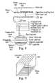
- FIG. 8illustrates a stackup of an exemplary double-sided touch panel along with a cover and liquid crystal display (LCD) according to one embodiment of this invention.
- LCDliquid crystal display
- FIG. 9is a perspective view of an exemplary DITO substrate (with its thickness greatly exaggerated for purposes of illustration only) illustrating the widening of rows for shielding purposes and for providing a uniform appearance according to one embodiment of this invention.
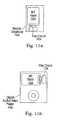
- FIG. 10 aillustrates an exemplary mobile telephone that can include the capacitive touch sensor panel and a flex circuit capable of connecting to both sides of the substrate according to one embodiment of this invention.
- FIG. 10 billustrates an exemplary digital audio player that can include the capacitive touch sensor panel and a flex circuit capable of connecting to both sides of the substrate according to one embodiment of this invention.
- Multi-touch sensor panels and their associated sensor panel circuitrymay be able to detect multiple touches (touch events or contact points) that occur at about the same time, and identify and track their locations.
- FIG. 1illustrates exemplary computing system 100 operable with capacitive multi-touch sensor panel 124 according to embodiments of this invention.
- Multi-touch sensor panel 124can be created using a substrate with column and row traces formed on either side of the substrate using a novel fabrication process. Flex circuits can be used to connect the column and row traces on either side of the sensor panel to its associated sensor panel circuitry.
- Traces made of copper or other highly conductive metals running along the edge of the substratecan be used to bring the row traces to the same edge of the substrate as the column traces so that the flex circuits can be bonded to the same edge of the substrate on directly opposing sides of the substrate, minimizing the area needed for connectivity and reducing the overall size of the sensor panel.
- a single flex circuitcan be fabricated to connect to the rows and columns on directly opposing sides at the same edge of the substrate.
- the row tracescan be widened to shield the column traces from a modulated Vcom layer.
- Computing system 100can include one or more panel processors 102 and peripherals 104 , and panel subsystem 106 .
- the one or more processors 102can include, for example, an ARM968 processors or other processors with similar functionality and capabilities.
- the panel processor functionalitycan be implemented instead by dedicated logic such as a state machine.
- Peripherals 104can include, but are not limited to, random access memory (RAM) or other types of memory or storage, watchdog timers and the like.
- Panel subsystem 106can include, but is not limited to, one or more analog channels 108 , channel scan logic 110 and driver logic 114 .
- Channel scan logic 110can access RAM 112 , autonomously read data from the analog channels and provide control for the analog channels. This control can include multiplexing columns of multi-touch panel 124 to analog channels 108 .
- channel scan logic 110can control the driver logic and stimulation signals being selectively applied to rows of multi-touch panel 124 .
- panel subsystem 106 , panel processor 102 and peripherals 104can be integrated into a single application specific integrated circuit (ASIC).
- ASICapplication specific integrated circuit
- Driver logic 114can provide multiple panel subsystem outputs 116 and can present a proprietary interface that drives high voltage driver, which is comprised of decoder 120 and subsequent level shifter and driver stage 118 , although level-shifting functions could be performed before decoder functions.
- Level shifter and driver 118can provide level shifting from a low voltage level (e.g. CMOS levels) to a higher voltage level, providing a better signal-to-noise (S/N) ratio for noise reduction purposes.
- Decoder 120can decode the drive interface signals to one out of N outputs, whereas N is the maximum number of rows in the panel. Decoder 120 can be used to reduce the number of drive lines needed between the high voltage driver and panel 124 .
- Each panel row input 122can drive one or more rows in panel 124 .
- driver 118 and decoder 120can be integrated into a single ASIC. However, in other embodiments driver 118 and decoder 120 can be integrated into driver logic 114 , and in still other embodiments driver 118 and decoder 120 can be eliminated entirely.
- Computing system 100can also include host processor 128 for receiving outputs from panel processor 102 and performing actions based on the outputs that can include, but are not limited to, moving an object such as a cursor or pointer, scrolling or panning, adjusting control settings, opening a file or document, viewing a menu, making a selection, executing instructions, operating a peripheral device connected to the host device, answering a telephone call, placing a telephone call, terminating a telephone call, changing the volume or audio settings, storing information related to telephone communications such as addresses, frequently dialed numbers, received calls, missed calls, logging onto a computer or a computer network, permitting authorized individuals access to restricted areas of the computer or computer network, loading a user profile associated with a user's preferred arrangement of the computer desktop, permitting access to web content, launching a particular program, encrypting or decoding a message, and/or the like.
- Host processor 128can also perform additional functions that may not be related to panel processing, and can be coupled to program storage 132 and display device 130 such
- multi-touch panel 124can in some embodiments include a capacitive sensing medium having a plurality of row traces or driving lines and a plurality of column traces or sensing lines (although other sensing media may also be used) separated by a dielectric.
- the dielectric materialcan be transparent, such as glass, or can be formed from other materials such as Mylar.
- the row and column tracescan be formed from a transparent conductive medium such as ITO or ATO, although other transparent or non-transparent materials such as copper can also be used.
- the row and column tracescan be perpendicular to each other, although in other embodiments other non-orthogonal and non-Cartesian orientations are possible.
- the sensing linescan be concentric circles and the driving lines can be radially extending lines (or vice versa).
- the terms “row” and “column,” “first dimension” and “second dimension,” or “first axis” and “second axis” as may be used hereinare intended to encompass not only orthogonal grids, but the intersecting traces of other geometric configurations having first and second dimensions (e.g. the concentric and radial lines of a polar-coordinate arrangement).
- each intersection of row and column tracescan represent a capacitive sensing node and can be viewed as picture element (pixel) 126 , which can be particularly useful when multi-touch panel 124 is viewed as capturing an “image” of touch.
- pixelpicture element
- the capacitance between row and column electrodesappears as a stray capacitance on all columns when the given row is held at DC and as a mutual capacitance Csig when the given row is stimulated with an AC signal.
- the presence of a finger or other object near or on the multi-touch panelcan be detected by measuring changes to Csig.
- the columns of multi-touch panel 124can drive one or more analog channels 108 (also referred to herein as event detection and demodulation circuits) in multi-touch subsystem 106 .
- each columnis coupled to one dedicated analog channel 108 .
- the columnsmay be couplable via an analog switch to a fewer number of analog channels 108 .
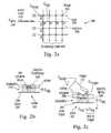
- FIG. 2 aillustrates exemplary capacitive multi-touch panel 200 .
- FIG. 2 aindicates the presence of a stray capacitance Cstray at each pixel 202 located at the intersection of a row 204 and a column 206 trace (although Cstray for only one column is illustrated in FIG. 2 for purposes of simplifying the figure).
- FIG. 2 aillustrates rows 204 and columns 206 as being substantially perpendicular, they need not be so aligned, as described above.
- Each of columns 206may be selectively connectable to one or more analog channels (see analog channels 108 in FIG. 1 ).
- FIG. 2 bis a side view of exemplary pixel 202 in a steady-state (no-touch) condition.
- an electric field of electric field lines 208 of the mutual capacitance between column 206 and row 204 traces or electrodes separated by dielectric 210is shown.
- FIG. 2 cis a side view of exemplary pixel 202 in a dynamic (touch) condition.
- finger 212has been placed near pixel 202 .
- Finger 212is a low-impedance object at signal frequencies, and has an AC capacitance Cfinger from the column trace 204 to the body.
- the bodyhas a self-capacitance to ground Cbody of about 200 pF, where Cbody is much larger than Cfinger.
- finger 212blocks some electric field lines 208 between the row and column electrodes (those fringing fields that exit the dielectric and pass through the air above the row electrode), those electric field lines are shunted to ground through the capacitance path inherent in the finger and the body, and as a result, the steady state signal capacitance Csig is reduced by ⁇ Csig.
- the combined body and finger capacitanceact to reduce Csig by an amount ⁇ Csig (which can also be referred to herein as Csig_sense), and can act as a shunt or dynamic return path to ground, blocking some of the electric fields as resulting in a reduced net signal capacitance.
- the signal capacitance at the pixelbecomes Csig ⁇ Csig, where Csig represents the static (no touch) component and ⁇ Csig represents the dynamic (touch) component.
- Csig ⁇ Csigmay always be nonzero due to the inability of a finger, palm or other object to block all electric fields, especially those electric fields that remain entirely within the dielectric material.
- ⁇ Csigcan be variable and representative of how completely the finger is pushing down on the panel (i.e. a range from “no-touch” to “full-touch”).
- Vstim signal 214can be applied to a row in multi-touch panel 200 so that a change in signal capacitance can be detected when a finger, palm or other object is present.
- Vstim signal 214can be generated as one or more pulse trains 216 at a particular frequency, with each pulse train including a number of pulses.
- pulse trains 216are shown as square waves, other waveshapes such as sine waves can also be employed.
- a plurality of pulse trains 216 at different frequenciescan be transmitted for noise reduction purposes to detect and avoid noisy frequencies.
- Vstim signal 214essentially injects a charge into the row, and can be applied to one row of multi-touch panel 200 at a time while all other rows are held at a DC level.
- the multi-touch panelcan be divided into two or more sections, with Vstim signal 214 being simultaneously applied to one row in each section and all other rows in that region section held at a DC voltage.
- Each analog channel coupled to a columnmeasures the mutual capacitance formed between that column and the row.
- This mutual capacitanceis comprised of the signal capacitance Csig and any change Csig_sense in that signal capacitance due to the presence of a finger, palm or other body part or object.
- These column values provided by the analog channelsmay be provided in parallel while a single row is being stimulated, or may be provided in series. If all of the values representing the signal capacitances for the columns have been obtained, another row in multi-touch panel 200 can be stimulated with all others held at a DC voltage, and the column signal capacitance measurements can be repeated. Eventually, if Vstim has been applied to all rows, and the signal capacitance values for all columns in all rows have been captured (i.e.
- a “snapshot” of all pixel valuescan be obtained for the entire multi-touch panel 200 .
- This snapshot datacan be initially saved in the multi-touch subsystem, and later transferred out for interpretation by other devices in the computing system such as the host processor. As multiple snapshots are obtained, saved and interpreted by the computing system, it is possible for multiple touches to be detected, tracked, and used to perform other functions.
- the rowsmay be either stimulated with an AC signal or held at a DC voltage level
- the columnsneed to be connected to analog channels so that modulated output signals can be detected, demodulated and converted to output values, electrical connections must be formed with the rows and columns on either side of the dielectric of the sensor panel.
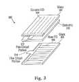
- FIG. 3is an exploded perspective view of an exemplary capacitive touch sensor panel 300 formed from a top layer of glass 302 upon which transparent column traces of ITO 304 have been etched, and a bottom layer of glass 306 upon which row traces of ITO 308 have been etched.
- the top and bottom glass layers 302 and 306are separated by a clear polymer spacer 310 that acts as a dielectric between the row and column traces. Because the rows and columns are perpendicular to each other, the most straightforward way to connect to these rows and columns is to bond flex circuit 312 at one edge of the sensor panel, and bond another flex circuit 314 on an adjacent edge of the sensor panel. However, because the connection areas for these flex circuits 312 and 314 are not on the same edge of sensor panel 300 and are not on directly opposing sides of dielectric 310 , the sensor panel must be made larger to accommodate these two non-overlapping connection areas.
- Capacitive touch sensor panelstypically form the row and column traces on two pieces of glass as shown in FIG. 3 because it has not been practical to form column and row traces on either side of a single substrate.
- Conventional methods for forming ITO traces on one side of a substraterequire that the substrate be placed on rollers during the fabrication process. However, if the substrate is then flipped over to form ITO traces on the second side, the rollers will damage any traces previously formed on the first side of the substrate.
- etchingis used to etch away part of the ITO to form traces on one side of the substrate, the entire substrate is conventionally placed in an etching bath, which will etch away any traces previously formed on the other side of the substrate.
- FIG. 4illustrates an exemplary capacitive touch sensor panel 400 fabricated using a double-sided ITO (DITO) substrate 402 having column and row ITO traces 404 and 406 , respectively, formed on either side of the substrate, and bonded between cover 408 and LCD 410 using transparent adhesive 412 according to embodiments of this invention.
- Substrate 402can be formed from glass, plastic, hybrid glass/plastic materials, and the like.
- Cover 408can be formed from glass, acrylic, sapphire, and the like.
- two flex circuit portions 414can be bonded to directly opposing sides at the same edge of DITO 402 , although other bonding locations may also be employed.
- FIG. 5is an exploded perspective view of an exemplary DITO substrate 500 (with its thickness greatly exaggerated for purposes of illustration only) with columns 502 and rows 508 formed on either side according to embodiments of this invention.
- Some of column ITO traces 502 on the top sideare routed to a necked-down connector area 504 , where they are brought off the panel by a flex circuit portion 506 that can be conductively bonded to the top of DITO substrate 500 .
- row ITO traces 508 on the bottom sidecan be connected to thin metal traces 510 that run alongside the edges of the bottom side.
- Metal traces 510can be routed to connector area 512 , which can be directly opposing connector area 504 , or at least on the same edge of DITO substrate 500 as connector area 504 . Providing connector areas 504 and 512 at the same edge of DITO substrate 500 can allow the substrate and therefore the product to be smaller.
- Another flex circuit portion 514can be used to bring row ITO traces 508 off the panel.
- Column and row ITO traces 502 and 508can be formed on both sides of DITO substrate 500 using several fabrication methods.
- a substratecan be placed on the rollers of the fabrication machinery and a layer of ITO can be sputtered onto a first side of DITO substrate 500 and etched (e.g. using photolithography techniques) to form column traces 502 .
- a protective coating of photoresiste.g. two layers of photoresist
- DITO substrate 500can be flipped over so that the rollers make contact only with the applied photoresist on the first side and not the formed column traces.
- Another layer of ITOcan then be sputtered onto the now-exposed back side of DITO substrate 500 and etched to form row traces 508 .
- the photoresist on the first sidecan be stripped off to complete the process.
- a protective coating of photoresiste.g. two layers of photoresist
- a metal layercan then be sputtered over the photoresist and exposed edges, and the metal layer can then be etched to form metal traces 510 at the edges. Finally, all remaining layers of photoresist can be stripped off.
- the second side of the DITO substrate patterningmay be formed by first patterning a photoresist using very simple geometry to cover only the interior region of the second side of the DITO substrate while leaving the edge regions exposed.
- metalis sputtered first and then the photoresist with simple geometry is then stripped off to leave metal in the edge regions only.
- the ITOis sputtered over the entire second side of the DITO substrate.
- a second photoresistis applied and patterned to form the mask for the electrode patterns.
- a series of etching stepsis then used to form the electrode pattern in the topmost ITO layer and metal layer underneath. The first etching steps etches the ITO only, and the second etch steps etches the metal layer only which produces the desired electrode geometry.
- FIG. 6illustrates an exemplary flex circuit 600 according to embodiments of this invention, including flex circuit portions 606 and 614 for connecting to the row and column traces, respectively, on either side of a DITO substrate, and flex circuit portion 608 for connecting to a host processor.
- Flex circuit 600includes a circuit area 602 upon which the multi-touch subsystem, multi-touch panel processor, the high voltage driver and decoder circuitry (see FIG. 1 ), an EEPROM and some essential small components such as bypass capacitors can be mounted and connected to save space.
- Circuit area 602may be shielded by an EMI can (not shown) which encloses circuit area 602 using top and bottom shield portions. The bottom can may be adhered to a structure of the device to secure the circuit area. From this circuit area 602 , flex circuit 600 may connect to the top of the DITO substrate via flex circuit portion 606 , to the bottom of the DITO substrate via flex circuit portion 614 , and to a host processor via flex circuit portion 608 .
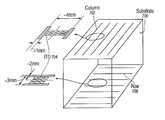
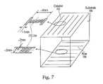
- FIG. 7is an exploded perspective view of an exemplary DITO substrate 700 (with its thickness greatly exaggerated for purposes of illustration only) with columns 702 and rows 708 formed on either side.
- column traces 702can be about 1 mm wide, with a spacing of about 4 mm between the traces
- row traces 708can be about 2 mm wide, with a spacing of about 3 mm between the rows.
- small isolated squares of ITO 704can be formed between the column and row traces 702 and 708 on either side of DITO substrate 700 , with narrow spacing (e.g. about 30 microns) between the isolated squares of ITO, so that either side of the DITO substrate provides a uniform appearance similar to a solid sheet of ITO.
- FIG. 8illustrates a stackup of an exemplary double-sided touch panel 800 along with cover 802 and liquid crystal display (LCD) 804 according to embodiments of this invention.
- LCD 804can include polarizer 806 , top glass layer 808 , liquid crystal layer 810 , bottom glass layer 812 , polarizer 814 , and backlight 816 .
- liquid crystal layer 810can include RGB color filter layer 818 , planarization layer 820 , a conductive unpatterned layer of ITO referred to as Vcom layer 822 , polyamide layer 824 , liquid crystal layer 826 , and polyamide layer 828 .
- Beneath polyamide layer 828is a layer of ITO rectangles and TFTs (collectively referred to herein as TFT layer 830 ), with one ITO rectangle and TFT for each sub-pixel (where three sub-pixels comprise a pixel).
- Color filter layer 818provides the three RGB colors that make up each pixel when illuminated by light, wherein the ratio of colors determines the color of that pixel.
- Planarization layer 820can be formed from clear plastic to smooth out the surface of color filter layer 818 .
- Vcomstands for “Voltage common” because Vcom layer 822 provides a common voltage for the ITO subpixels of TFT layer 830 .
- Vcom layer 822may be maintained at a constant voltage (LCDs using a constant Vcom voltage may be referred to as DC or constant Vcom LCDs) or modulated with an AC signal.
- Polyamide layers 824 and 828serve to pre-align the orientation of liquid crystals in liquid crystal layer 826 .
- the ITO squares for each subpixel in TFT layer 830can have voltages applied to them with respect to Vcom layer 822 , which causes the liquid crystals to align and allow light from backlight 816 to pass through liquid crystal layer 826 and through the RGB color filters in color filter layer 818 .
- Vcom layer 822can be held constant, in some embodiments the Vcom layer can be driven by a modulated signal (e.g. a squareware from about 1 to 4 volts).
- a modulated signale.g. a squareware from about 1 to 4 volts.
- the modulated signalmay be capacitively coupled (see reference character 834 ) through the sparse conductors of rows 836 on the bottom of double-sided touch panel 800 and onto columns 838 , causing noise on the columns.
- rows 836are referred to as “sparse,” even though it includes many closely spaced ITO squares, because the squares are isolated and therefore of negligible effect from a shielding standpoint.
- modulated Vcom layer 822is also capacitively coupled onto rows 836 , because the rows are being driven by driver circuitry with low impedance outputs, any capacitive coupling is shunted to the driver outputs, and has negligible effect.
- columns 838are designed to sense small changes in the AC capacitance of the touch panel, so the capacitive coupling from modulated Vcom layer 822 can easily be seen as noise at the analog channels receiving the columns.
- FIG. 9is a perspective view of an exemplary DITO substrate 900 (with its thickness greatly exaggerated for purposes of illustration only) illustrating the widening of rows 936 for shielding purposes and for providing a uniform appearance according to embodiments of this invention.
- rows 936may be widened as shown in FIG. 9 .
- the number of rows 936does not change, but they are now much wider (e.g. about 4.97 mm), leaving only about 30 microns of space between them.
- these wider rows 936are not isolated but are instead either held at a DC voltage or stimulated with a stimulation voltage, these wider rows 936 act as a shield, preventing a modulated Vcom layer from capacitively coupling onto columns 938 .
- rows 936provide a uniform appearance.
- shielding, modulation and a uniform appearancecan be obtained from a single layer of ITO.
- FIG. 9illustrates rows and columns formed on opposite sides of a single substrate, wide rows can also be employed on the otherwise conventional touch sensor panel shown in FIG. 3 .
- An alternative to these wide rowsis to add another layer of ITO as a shield between the LCD and DITO, but this would represent extra cost, extra thickness, light loss, and unwanted color shift.
- top side of an exemplary DITO substratemay include isolated ITO squares between rows, and a bottom side may include wide rows.
- Outer row tracescan be routed to a first flex connector area on the top side via traces.
- Rows on the bottom sidecan be routed to second flex connector areas via metal traces running along the long edges of the bottom side. Note that the second flex connector areas can be located on the same edge of the DITO substrate as the first flex connector, but the conductors themselves are located in non-overlapping areas to make bonding of flex circuits easier.
- FIG. 10 aillustrates an exemplary mobile telephone 1136 that can include capacitive touch sensor panel 1124 and flex circuit 1134 capable of connecting to both sides of the substrate according to embodiments of this invention.
- Sensor panel 1124can be fabricated using a substrate having column and row ITO traces formed on either side of the substrate, and metal traces form along the edges of one side of the substrate to allow flex circuit connection areas to be located on opposing sides of the same edge of the substrate.
- sensor panel 1134can be fabricated with wide rows to provide modulated Vcom layer shielding as well as a uniform appearance.
- FIGS. 10 billustrates an exemplary digital audio/video player 1138 that can include capacitive touch sensor panel 1124 and flex circuit 1134 capable of connecting to both sides of the substrate according to embodiments of this invention.
- Sensor panel 1124can be fabricated using a substrate having column and row ITO traces formed on either side of the substrate, and metal traces form along the edges of one side of the substrate to allow flex circuit connection areas to be located on opposing sides of the same edge of the substrate.
- sensor panel 1134can be fabricated with wide rows to provide modulated Vcom layer shielding as well as a uniform appearance.
- 10 a and 10 bcan advantageously benefit from sensor panel 1124 because a single, thinner, smaller-sized sensor panel can be used, and only a single layer of ITO is needed to provide shielding and a uniform appearance. The overall effect is reduced product size and manufacturing costs.
Landscapes
- Engineering & Computer Science (AREA)
- Theoretical Computer Science (AREA)
- General Engineering & Computer Science (AREA)
- Physics & Mathematics (AREA)
- General Physics & Mathematics (AREA)
- Human Computer Interaction (AREA)
- Computer Hardware Design (AREA)
- Nonlinear Science (AREA)
- Computer Networks & Wireless Communication (AREA)
- Mathematical Physics (AREA)
- Chemical & Material Sciences (AREA)
- Crystallography & Structural Chemistry (AREA)
- Optics & Photonics (AREA)
- Position Input By Displaying (AREA)
- Switches That Are Operated By Magnetic Or Electric Fields (AREA)
Abstract
Description
This application is a continuation of U.S. patent application Ser. No. 11/650,182, filed Jan. 3, 2007, the disclosure of which is incorporated herein by reference in its entirety for all purposes.
This invention relates to touch sensor panels, and more particularly, to capacitive multi-touch sensor panels having rows and columns formed on either sides of the same substrate.
Many types of input devices are presently available for performing operations in a computing system, such as buttons or keys, mice, trackballs, touch panels, joysticks, touch screens and the like. Touch screens, in particular, are becoming increasingly popular because of their ease and versatility of operation as well as their declining price. Touch screens can include a touch panel, which can be a clear panel with a touch-sensitive surface. The touch panel can be positioned in front of a display screen so that the touch-sensitive surface covers the viewable area of the display screen. Touch screens can allow a user to make selections and move a cursor by simply touching the display screen via a finger or stylus. In general, the touch screen can recognize the touch and position of the touch on the display screen, and the computing system can interpret the touch and thereafter perform an action based on the touch event.
Touch panels can include an array of touch sensors capable of detecting touch events (the touching of fingers or other objects upon a touch-sensitive surface). Future panels may be able to detect multiple touches (the touching of fingers or other objects upon a touch-sensitive surface at distinct locations at about the same time) and near touches (fingers or other objects within the near-field detection capabilities of their touch sensors), and identify and track their locations. Examples of multi-touch panels are described in Applicant's co-pending U.S. application Ser. No. 10/842,862 entitled “Multipoint Touchscreen,” filed on May 6, 2004 and published as U.S. Published Application No. 2006/0097991 on May 11, 2006, the contents of which are incorporated by reference herein.
Capacitive touch sensor panels can be formed from rows and columns of traces on opposite sides of a dielectric. At the “intersections” of the traces, where the traces pass above and below each other (but do not make direct electrical contact with each other), the traces essentially form two electrodes. Conventional touch panels for use over display devices have typically utilized a top layer of glass upon which transparent column traces of indium tin oxide (ITO) or antimony tin oxide (ATO) have been etched, and a bottom layer of glass upon which row traces of ITO have been etched. However, the use of transparent traces is not required if the conductors are thin enough (on the order of 30 microns). In addition, if panel transparency is not required (e.g. the touch panel is not being used over a display device), the conductors can be made out of an opaque material such as copper. The top and bottom glass layers are separated by a clear polymer spacer that acts as a dielectric between the row and column traces. The traces on both the top and bottom glass layers can have a spacing of about 5 mm.
To scan a sensor panel, a stimulus can be applied to one row with all other rows held at DC voltage levels. When a row is stimulated, a modulated output signal can be capacitively coupled onto the columns of the sensor panel. The columns can be connected to analog channels (also referred to herein as event detection and demodulation circuits). For every row that is stimulated, each analog channel connected to a column generates an output value representative of an amount of change in the modulated output signal due to a touch or hover event occurring at the sensor located at the intersection of the stimulated row and the connected column. After analog channel output values are obtained for every column in the sensor panel, a new row is stimulated (with all other rows once again held at DC voltage levels), and additional analog channel output values are obtained. When all rows have been stimulated and analog channel output values have been obtained, the sensor panel is said to have been “scanned,” and a complete “image” of touch or hover can be obtained over the entire sensor panel. This image of touch or hover can include an analog channel output value for every pixel (row and column) in the panel, each output value representative of the amount of touch or hover that was detected at that particular location.
Because the rows must be either stimulated with an AC signal or held at a DC voltage level, and because the columns must be connected to analog channels so that modulated output signals can be detected, demodulated and converted to output values, electrical connections must be formed with the rows and columns on either side of the dielectric of the sensor panel. Because the rows and columns are perpendicular to each other, the most straightforward way to connect to these rows and columns is to bond a flex circuit at one edge of the sensor panel (e.g. the shorter side of a rectangular panel) to provide connections to the columns, and bond another flex circuit on an adjacent edge of the sensor panel (e.g. the longer side of a rectangular panel) to provide connections to the rows. However, because these flex circuit connections areas are not on the same edge of the sensor panel and are not on directly opposing sides of the dielectric, the sensor panel must be made larger to accommodate these two non-overlapping connection areas.
Furthermore, when a transparent capacitive touch sensor panel is bonded to a liquid crystal display (LCD), a modulated Vcom layer in the LCD can couple onto the columns of the sensor panel, causing noise to appear on the columns.
A multi-touch sensor panel can be created using a substrate with column and row traces formed on either side of the substrate using a novel fabrication process. Flex circuits can be used to connect the column and row traces on either side of the sensor panel to its associated sensor panel circuitry. Traces made of copper or other highly conductive metals running along the edge of the substrate can be used to bring the row traces to the same edge of the substrate as the column traces so that the flex circuits can be bonded to the same edge of the substrate on directly opposing sides of the substrate, minimizing the area needed for connectivity and reducing the overall size of the sensor panel. A single flex circuit can be fabricated to connect to the rows and columns on directly opposing sides at the same edge of the substrate. Furthermore, the row traces can be widened to shield the column traces from a modulated Vcom layer.
Column and row ITO traces can be formed on both sides of a DITO substrate using several fabrication methods. In one embodiment, a substrate can be placed on the rollers of the fabrication machinery and a layer of ITO can be sputtered onto a first side of the DITO substrate and etched (e.g. using photolithography techniques) to form the column traces. A protective coating of photoresist (e.g. two layers of photoresist) can then be applied over the column traces, and the DITO substrate can be flipped over so that the rollers make contact only with the applied photoresist on the first side and not the formed column traces. Another layer of ITO can then be sputtered onto the now-exposed back side of the DITO substrate and etched to formrow traces 508.
If no metal traces are required, the photoresist on the first side can be stripped off to complete the process. However, if metal traces are required at the edges to connect to the row traces and bring them to a particular edge of the substrate, a protective coating of photoresist (e.g. two layers of photoresist) can be applied over the row traces, leaving the edges exposed. A metal layer can then be sputtered over the photoresist and exposed edges, and the metal layer can then be etched to form metal traces at the edges. Finally, all remaining layers of photoresist can be stripped off.
Flex circuit portions on a single flex circuit can be formed for connecting to the row and column traces, respectively, on either side of a DITO substrate, and to a host processor. The flex circuit can also include a circuit area upon which a multi-touch subsystem, multi-touch panel processor, high voltage driver and decoder circuitry, an EEPROM and some essential small components such as bypass capacitors can be mounted and connected to save space.
The rows of the DITO substrate can also be widened for shielding purposes and for providing a uniform appearance according to embodiments of this invention. To prevent the capacitive coupling of a modulated Vcom layer onto the columns of the substrate, the rows may be widened. The number of rows does not change, but they can be much wider, leaving only about 30 microns of space between them. Because these wider rows are not isolated but are instead either held at a DC voltage or stimulated with a stimulation voltage, these wider rows act as a shield, preventing a modulated Vcom layer from capacitively coupling onto the columns. In addition, because of the narrow spacing between them, the wide rows provide a uniform appearance. Thus, shielding, modulation and a uniform appearance can be obtained from a single layer of ITO.
In the following description of preferred embodiments, reference is made to the accompanying drawings which form a part hereof, and in which it is shown by way of illustration specific embodiments in which the invention may be practiced. It is to be understood that other embodiments may be utilized and structural changes may be made without departing from the scope of the preferred embodiments of the present invention.
Multi-touch sensor panels and their associated sensor panel circuitry may be able to detect multiple touches (touch events or contact points) that occur at about the same time, and identify and track their locations.FIG. 1 illustratesexemplary computing system 100 operable with capacitivemulti-touch sensor panel 124 according to embodiments of this invention.Multi-touch sensor panel 124 can be created using a substrate with column and row traces formed on either side of the substrate using a novel fabrication process. Flex circuits can be used to connect the column and row traces on either side of the sensor panel to its associated sensor panel circuitry. Traces made of copper or other highly conductive metals running along the edge of the substrate can be used to bring the row traces to the same edge of the substrate as the column traces so that the flex circuits can be bonded to the same edge of the substrate on directly opposing sides of the substrate, minimizing the area needed for connectivity and reducing the overall size of the sensor panel. A single flex circuit can be fabricated to connect to the rows and columns on directly opposing sides at the same edge of the substrate. Furthermore, the row traces can be widened to shield the column traces from a modulated Vcom layer.
As mentioned above,multi-touch panel 124 can in some embodiments include a capacitive sensing medium having a plurality of row traces or driving lines and a plurality of column traces or sensing lines (although other sensing media may also be used) separated by a dielectric. In some embodiments, the dielectric material can be transparent, such as glass, or can be formed from other materials such as Mylar. The row and column traces can be formed from a transparent conductive medium such as ITO or ATO, although other transparent or non-transparent materials such as copper can also be used. In some embodiments, the row and column traces can be perpendicular to each other, although in other embodiments other non-orthogonal and non-Cartesian orientations are possible. For example, in a polar coordinate system, the sensing lines can be concentric circles and the driving lines can be radially extending lines (or vice versa). It should be understood, therefore, that the terms “row” and “column,” “first dimension” and “second dimension,” or “first axis” and “second axis” as may be used herein are intended to encompass not only orthogonal grids, but the intersecting traces of other geometric configurations having first and second dimensions (e.g. the concentric and radial lines of a polar-coordinate arrangement).
At the “intersections” of the traces, where the traces pass above and below each other (but do not make direct electrical contact with each other), the traces essentially form two electrodes (although more than two traces could intersect as well). Each intersection of row and column traces can represent a capacitive sensing node and can be viewed as picture element (pixel)126, which can be particularly useful whenmulti-touch panel 124 is viewed as capturing an “image” of touch. (In other words, aftermulti-touch subsystem 106 has determined whether a touch event has been detected at each touch sensor in the multi-touch panel, the pattern of touch sensors in the multi-touch panel at which a touch event occurred can be viewed as an “image” of touch (e.g. a pattern of fingers touching the panel).) The capacitance between row and column electrodes appears as a stray capacitance on all columns when the given row is held at DC and as a mutual capacitance Csig when the given row is stimulated with an AC signal. The presence of a finger or other object near or on the multi-touch panel can be detected by measuring changes to Csig. The columns ofmulti-touch panel 124 can drive one or more analog channels108 (also referred to herein as event detection and demodulation circuits) inmulti-touch subsystem 106. In some embodiments, each column is coupled to onededicated analog channel 108. However, in other embodiments, the columns may be couplable via an analog switch to a fewer number ofanalog channels 108.
Referring again toFIG. 2 a, as mentioned above, Vstim signal214 can be applied to a row inmulti-touch panel 200 so that a change in signal capacitance can be detected when a finger, palm or other object is present.Vstim signal 214 can be generated as one or more pulse trains216 at a particular frequency, with each pulse train including a number of pulses. Although pulse trains216 are shown as square waves, other waveshapes such as sine waves can also be employed. A plurality of pulse trains216 at different frequencies can be transmitted for noise reduction purposes to detect and avoid noisy frequencies.Vstim signal 214 essentially injects a charge into the row, and can be applied to one row ofmulti-touch panel 200 at a time while all other rows are held at a DC level. However, in other embodiments, the multi-touch panel can be divided into two or more sections, withVstim signal 214 being simultaneously applied to one row in each section and all other rows in that region section held at a DC voltage.
Each analog channel coupled to a column measures the mutual capacitance formed between that column and the row. This mutual capacitance is comprised of the signal capacitance Csig and any change Csig_sense in that signal capacitance due to the presence of a finger, palm or other body part or object. These column values provided by the analog channels may be provided in parallel while a single row is being stimulated, or may be provided in series. If all of the values representing the signal capacitances for the columns have been obtained, another row inmulti-touch panel 200 can be stimulated with all others held at a DC voltage, and the column signal capacitance measurements can be repeated. Eventually, if Vstim has been applied to all rows, and the signal capacitance values for all columns in all rows have been captured (i.e. the entiremulti-touch panel 200 has been “scanned”), a “snapshot” of all pixel values can be obtained for the entiremulti-touch panel 200. This snapshot data can be initially saved in the multi-touch subsystem, and later transferred out for interpretation by other devices in the computing system such as the host processor. As multiple snapshots are obtained, saved and interpreted by the computing system, it is possible for multiple touches to be detected, tracked, and used to perform other functions.
As described above, because the rows may be either stimulated with an AC signal or held at a DC voltage level, and because the columns need to be connected to analog channels so that modulated output signals can be detected, demodulated and converted to output values, electrical connections must be formed with the rows and columns on either side of the dielectric of the sensor panel.
Capacitive touch sensor panels typically form the row and column traces on two pieces of glass as shown inFIG. 3 because it has not been practical to form column and row traces on either side of a single substrate. Conventional methods for forming ITO traces on one side of a substrate require that the substrate be placed on rollers during the fabrication process. However, if the substrate is then flipped over to form ITO traces on the second side, the rollers will damage any traces previously formed on the first side of the substrate. Furthermore, when etching is used to etch away part of the ITO to form traces on one side of the substrate, the entire substrate is conventionally placed in an etching bath, which will etch away any traces previously formed on the other side of the substrate.
Column and row ITO traces502 and508 can be formed on both sides of DITO substrate500 using several fabrication methods. In one embodiment, a substrate can be placed on the rollers of the fabrication machinery and a layer of ITO can be sputtered onto a first side of DITO substrate500 and etched (e.g. using photolithography techniques) to form column traces502. A protective coating of photoresist (e.g. two layers of photoresist) can then be applied over the column traces502, and DITO substrate500 can be flipped over so that the rollers make contact only with the applied photoresist on the first side and not the formed column traces. Another layer of ITO can then be sputtered onto the now-exposed back side of DITO substrate500 and etched to form row traces508.
If no metal traces510 are required, the photoresist on the first side can be stripped off to complete the process. However, if metal traces510 are required at the edges to connect to rowtraces 508 and bring them to a particular edge of the substrate, a protective coating of photoresist (e.g. two layers of photoresist) can be applied over row traces508, leaving the edges exposed. A metal layer can then be sputtered over the photoresist and exposed edges, and the metal layer can then be etched to form metal traces510 at the edges. Finally, all remaining layers of photoresist can be stripped off.
Minor variations to the process described above can also be made. For example, the second side of the DITO substrate patterning may be formed by first patterning a photoresist using very simple geometry to cover only the interior region of the second side of the DITO substrate while leaving the edge regions exposed. For this variation, metal is sputtered first and then the photoresist with simple geometry is then stripped off to leave metal in the edge regions only. Then the ITO is sputtered over the entire second side of the DITO substrate. A second photoresist is applied and patterned to form the mask for the electrode patterns. A series of etching steps is then used to form the electrode pattern in the topmost ITO layer and metal layer underneath. The first etching steps etches the ITO only, and the second etch steps etches the metal layer only which produces the desired electrode geometry.
From top to bottom, liquid crystal layer810 can include RGB color filter layer818,planarization layer 820, a conductive unpatterned layer of ITO referred to as Vcom layer822,polyamide layer 824, liquid crystal layer826, and polyamide layer828. Beneath polyamide layer828 is a layer of ITO rectangles and TFTs (collectively referred to herein as TFT layer830), with one ITO rectangle and TFT for each sub-pixel (where three sub-pixels comprise a pixel).
Color filter layer818 provides the three RGB colors that make up each pixel when illuminated by light, wherein the ratio of colors determines the color of that pixel.Planarization layer 820 can be formed from clear plastic to smooth out the surface of color filter layer818. Vcom stands for “Voltage common” because Vcom layer822 provides a common voltage for the ITO subpixels of TFT layer830. Vcom layer822 may be maintained at a constant voltage (LCDs using a constant Vcom voltage may be referred to as DC or constant Vcom LCDs) or modulated with an AC signal. Polyamide layers824 and828 serve to pre-align the orientation of liquid crystals in liquid crystal layer826. To create the color for one pixel, the ITO squares for each subpixel in TFT layer830 can have voltages applied to them with respect to Vcom layer822, which causes the liquid crystals to align and allow light from backlight816 to pass through liquid crystal layer826 and through the RGB color filters in color filter layer818.
As mentioned above, although Vcom layer822 can be held constant, in some embodiments the Vcom layer can be driven by a modulated signal (e.g. a squareware from about 1 to 4 volts). However, when Vcom layer822 is driven by a modulated signal, the modulated signal may be capacitively coupled (see reference character834) through the sparse conductors ofrows 836 on the bottom of double-sided touch panel 800 and ontocolumns 838, causing noise on the columns. Note thatrows 836 are referred to as “sparse,” even though it includes many closely spaced ITO squares, because the squares are isolated and therefore of negligible effect from a shielding standpoint. Note also that although modulated Vcom layer822 is also capacitively coupled ontorows 836, because the rows are being driven by driver circuitry with low impedance outputs, any capacitive coupling is shunted to the driver outputs, and has negligible effect. However,columns 838 are designed to sense small changes in the AC capacitance of the touch panel, so the capacitive coupling from modulated Vcom layer822 can easily be seen as noise at the analog channels receiving the columns.
As mentioned above, top side of an exemplary DITO substrate according to embodiments of the invention may include isolated ITO squares between rows, and a bottom side may include wide rows. Outer row traces can be routed to a first flex connector area on the top side via traces. Rows on the bottom side can be routed to second flex connector areas via metal traces running along the long edges of the bottom side. Note that the second flex connector areas can be located on the same edge of the DITO substrate as the first flex connector, but the conductors themselves are located in non-overlapping areas to make bonding of flex circuits easier.
Although the present invention has been fully described in connection with embodiments thereof with reference to the accompanying drawings, it is to be noted that various changes and modifications will become apparent to those skilled in the art. Such changes and modifications are to be understood as being included within the scope of the present invention as defined by the appended claims.
Claims (22)
1. A touch sensor panel, comprising:
a first set of traces of conductive material having lengths arranged along a first dimension of a two-dimensional coordinate system, an average width of the first set of traces over an entire length of the trace defining a first average width; and
a second set of traces of the conductive material spatially separated from the first set of traces by a dielectric having lengths arranged along a second dimension of the two-dimensional coordinate system, an average width of the second set of traces over an entire length of the trace defining a second average width;
wherein the second average width is substantially greater than the first average width to provide shielding for the first set of traces.
2. The touch sensor panel ofclaim 1 , wherein the plurality of second traces are coupled for receiving a stimulation signal.
3. The touch sensor panel ofclaim 1 , wherein sensors are formed at locations at which the first set of traces and the second set of traces pass above and below each other but do not make direct electrical contact with each other while separated by the dielectric.
4. The touch sensor panel ofclaim 1 , wherein the second average width is selected to provide an average spacing between the second set of traces of less than a predetermined amount to provide optical uniformity.
5. The touch sensor panel ofclaim 1 , the touch sensor panel incorporated into a touch-sensitive computing system.
6. The touch sensor panel ofclaim 1 , the touch sensor panel supported on a liquid crystal display (LCD) capable of emitting a modulated signal, wherein the second set of traces are configured for shielding the first set of traces from the modulated signal.
7. The touch sensor panel ofclaim 1 , the touch sensor panel coupled to a panel subsystem controller configured for sending stimulation signals to the second set of traces and receiving sense signals from the first set of traces.
8. A touch sensor panel, comprising:
a plurality of sense traces of conductive material each having an average width defining a sense trace average width; and
a plurality of drive traces of the conductive material spatially separated from the plurality of sense traces by a dielectric, the plurality of drive traces each having an average width defining a drive trace average width;
wherein the drive trace average width is substantially greater than the sense trace average width to provide shielding for the plurality of sense traces.
9. The touch sensor panel ofclaim 8 , wherein the plurality of drive traces are coupled for receiving a stimulation signal.
10. The touch sensor panel ofclaim 8 , wherein sensors are formed at locations at which the plurality of sense traces and the plurality of drive traces pass above and below each other but do not make direct electrical contact with each other while separated by the dielectric.
11. The touch sensor panel ofclaim 8 , wherein the drive trace average width of the plurality of drive traces is selected to provide an average spacing between the plurality of drive traces of less than a predetermined amount to provide optical uniformity.
12. The touch sensor panel ofclaim 8 , the touch sensor panel incorporated into a touch-sensitive computing system.
13. The touch sensor panel ofclaim 8 , the touch sensor panel supported on a liquid crystal display (LCD) capable of emitting a modulated signal, wherein the plurality of drive traces are configured for shielding the plurality of sense traces from the modulated signal.
14. The touch sensor panel ofclaim 8 , the touch sensor panel coupled to a panel subsystem controller configured for sending stimulation signals to the plurality of drive traces and receiving sense signals from the plurality of sense traces.
15. A method for shielding a touch sensor panel, comprising:
interposing a second layer of conductive material including a plurality of second traces between a first layer of the conductive material including a plurality of first traces and a noise source, the plurality of second traces having an average width defining a second average width and the plurality of first traces having an average width defining a first average width; and
configuring the plurality of second traces such that the second average width is substantially greater than the first average width to provide shielding for the first plurality of traces.
16. The method ofclaim 15 , further comprising coupling the plurality of second traces to a stimulation signal.
17. The method ofclaim 15 , further comprising arranging the plurality of second traces and the plurality of first traces to form sensors at locations at which the plurality of second traces and the plurality of first traces pass above and below each other but do not make direct electrical contact with each other.
18. The method ofclaim 15 , further comprising selecting the second average width of the second plurality of traces to provide an average spacing between the second plurality of traces of less than a predetermined amount to provide optical uniformity.
19. A computing device, comprising:
a circuit capable of emitting electromagnetic interference;
a touch sensor panel coupled to the circuit, the touch sensor panel including
a first set of traces of conductive material having lengths arranged along a first dimension of a two-dimensional coordinate system, an average width of the first set of traces over an entire length of the trace defining a first average width, and
a second set of traces of the conductive material spatially separated from the first set of traces by a dielectric having lengths arranged along a second dimension of the two-dimensional coordinate system, an average width of the second set of traces over an entire length of the trace defining a second average width,
wherein the second average width is substantially greater than the first average width to provide shielding for the first set of traces; and
a panel subsystem controller coupled to the touch sensor panel, the panel subsystem controller configured for sending stimulation signals to the second set of traces and receiving sense signals from the first set of traces.
20. The computing device ofclaim 19 , wherein sensors are formed at locations on the touch sensor panel at which the first set of traces and the second set of traces pass above and below each other but do not make direct electrical contact with each other while separated by a dielectric.
21. The computing device ofclaim 19 , wherein the second average width of the second set of traces is selected to provide an average spacing between the second set of traces of less than a predetermined amount to provide optical uniformity.
22. The computing device ofclaim 19 , wherein the second set of traces are coupled for receiving a stimulation signal.
Priority Applications (6)
| Application Number | Priority Date | Filing Date | Title |
|---|---|---|---|
| US13/078,789US8884890B2 (en) | 2007-01-03 | 2011-04-01 | Double-sided touch-sensitive panel with shield and drive combined layer |
| US14/340,262US9075491B2 (en) | 2007-01-03 | 2014-07-24 | Double-sided touch-sensitive panel with shield and drive combined layer |
| US14/734,998US9465502B2 (en) | 2007-01-03 | 2015-06-09 | Double-sided touch-sensitive panel with shield and drive combined layer |
| US15/268,421US9836160B2 (en) | 2007-01-03 | 2016-09-16 | Double-sided touch-sensitive panel with shield and drive combined layer |
| US15/830,375US10474287B2 (en) | 2007-01-03 | 2017-12-04 | Double-sided touch-sensitive panel with shield and drive combined layer |
| US16/672,187US11112904B2 (en) | 2007-01-03 | 2019-11-01 | Double-sided touch-sensitive panel with shield and drive combined layer |
Applications Claiming Priority (2)
| Application Number | Priority Date | Filing Date | Title |
|---|---|---|---|
| US11/650,182US7920129B2 (en) | 2007-01-03 | 2007-01-03 | Double-sided touch-sensitive panel with shield and drive combined layer |
| US13/078,789US8884890B2 (en) | 2007-01-03 | 2011-04-01 | Double-sided touch-sensitive panel with shield and drive combined layer |
Related Parent Applications (1)
| Application Number | Title | Priority Date | Filing Date |
|---|---|---|---|
| US11/650,182ContinuationUS7920129B2 (en) | 2007-01-03 | 2007-01-03 | Double-sided touch-sensitive panel with shield and drive combined layer |
Related Child Applications (1)
| Application Number | Title | Priority Date | Filing Date |
|---|---|---|---|
| US14/340,262ContinuationUS9075491B2 (en) | 2007-01-03 | 2014-07-24 | Double-sided touch-sensitive panel with shield and drive combined layer |
Publications (2)
| Publication Number | Publication Date |
|---|---|
| US20110181549A1 US20110181549A1 (en) | 2011-07-28 |
| US8884890B2true US8884890B2 (en) | 2014-11-11 |
Family
ID=39583204
Family Applications (7)
| Application Number | Title | Priority Date | Filing Date |
|---|---|---|---|
| US11/650,182Active2030-01-23US7920129B2 (en) | 2007-01-03 | 2007-01-03 | Double-sided touch-sensitive panel with shield and drive combined layer |
| US13/078,789Active2027-10-14US8884890B2 (en) | 2007-01-03 | 2011-04-01 | Double-sided touch-sensitive panel with shield and drive combined layer |
| US14/340,262ActiveUS9075491B2 (en) | 2007-01-03 | 2014-07-24 | Double-sided touch-sensitive panel with shield and drive combined layer |
| US14/734,998ActiveUS9465502B2 (en) | 2007-01-03 | 2015-06-09 | Double-sided touch-sensitive panel with shield and drive combined layer |
| US15/268,421ActiveUS9836160B2 (en) | 2007-01-03 | 2016-09-16 | Double-sided touch-sensitive panel with shield and drive combined layer |
| US15/830,375ActiveUS10474287B2 (en) | 2007-01-03 | 2017-12-04 | Double-sided touch-sensitive panel with shield and drive combined layer |
| US16/672,187ActiveUS11112904B2 (en) | 2007-01-03 | 2019-11-01 | Double-sided touch-sensitive panel with shield and drive combined layer |
Family Applications Before (1)
| Application Number | Title | Priority Date | Filing Date |
|---|---|---|---|
| US11/650,182Active2030-01-23US7920129B2 (en) | 2007-01-03 | 2007-01-03 | Double-sided touch-sensitive panel with shield and drive combined layer |
Family Applications After (5)
| Application Number | Title | Priority Date | Filing Date |
|---|---|---|---|
| US14/340,262ActiveUS9075491B2 (en) | 2007-01-03 | 2014-07-24 | Double-sided touch-sensitive panel with shield and drive combined layer |
| US14/734,998ActiveUS9465502B2 (en) | 2007-01-03 | 2015-06-09 | Double-sided touch-sensitive panel with shield and drive combined layer |
| US15/268,421ActiveUS9836160B2 (en) | 2007-01-03 | 2016-09-16 | Double-sided touch-sensitive panel with shield and drive combined layer |
| US15/830,375ActiveUS10474287B2 (en) | 2007-01-03 | 2017-12-04 | Double-sided touch-sensitive panel with shield and drive combined layer |
| US16/672,187ActiveUS11112904B2 (en) | 2007-01-03 | 2019-11-01 | Double-sided touch-sensitive panel with shield and drive combined layer |
Country Status (3)
| Country | Link |
|---|---|
| US (7) | US7920129B2 (en) |
| CN (2) | CN102176195B (en) |
| TW (4) | TWI398806B (en) |
Cited By (5)
| Publication number | Priority date | Publication date | Assignee | Title |
|---|---|---|---|---|
| US20140333857A1 (en)* | 2007-01-03 | 2014-11-13 | Apple Inc. | Double-sided touch-sensitive panel with shield and drive combined layer |
| US20160224185A1 (en)* | 2007-01-03 | 2016-08-04 | Apple Inc. | Front-end signal compensation |
| US10175832B2 (en) | 2011-12-22 | 2019-01-08 | Quickstep Technologies Llc | Switched-electrode capacitive-measurement device for touch-sensitive and contactless interfaces |
| US10503328B2 (en) | 2011-06-16 | 2019-12-10 | Quickstep Technologies Llc | Device and method for generating an electrical power supply in an electronic system with a variable reference potential |
| US10866681B2 (en) | 2016-08-22 | 2020-12-15 | Samsung Electronics Co., Ltd | Display device, electronic device including display device, and pressure sensing method therefor |
Families Citing this family (496)
| Publication number | Priority date | Publication date | Assignee | Title |
|---|---|---|---|---|
| GB9722766D0 (en) | 1997-10-28 | 1997-12-24 | British Telecomm | Portable computers |
| JP2002501271A (en) | 1998-01-26 | 2002-01-15 | ウェスターマン,ウェイン | Method and apparatus for integrating manual input |
| US7663607B2 (en) | 2004-05-06 | 2010-02-16 | Apple Inc. | Multipoint touchscreen |
| US7821425B2 (en) | 2002-07-12 | 2010-10-26 | Atmel Corporation | Capacitive keyboard with non-locking reduced keying ambiguity |
| GB0319714D0 (en) | 2003-08-21 | 2003-09-24 | Philipp Harald | Anisotropic touch screen element |
| DE212004000044U1 (en)* | 2003-08-21 | 2006-06-01 | Philipp, Harald, Hamble | Capacitive position sensor |
| GB2428306B (en) | 2005-07-08 | 2007-09-26 | Harald Philipp | Two-dimensional capacitive position sensor |
| US7932898B2 (en)* | 2005-09-20 | 2011-04-26 | Atmel Corporation | Touch sensitive screen |
| US8144125B2 (en) | 2006-03-30 | 2012-03-27 | Cypress Semiconductor Corporation | Apparatus and method for reducing average scan rate to detect a conductive object on a sensing device |
| DE202007005237U1 (en)* | 2006-04-25 | 2007-07-05 | Philipp, Harald, Southampton | Touch-sensitive position sensor for use in control panel, has bus bars arranged at distance to substrate, and detection region with units that are arranged at distance by non-conductive openings such that current flows into region |
| GB2437827B (en) | 2006-05-05 | 2008-03-26 | Harald Philipp | Touch screen element |
| US7903092B2 (en)* | 2006-05-25 | 2011-03-08 | Atmel Corporation | Capacitive keyboard with position dependent reduced keying ambiguity |
| US8619054B2 (en)* | 2006-05-31 | 2013-12-31 | Atmel Corporation | Two dimensional position sensor |
| US8552989B2 (en) | 2006-06-09 | 2013-10-08 | Apple Inc. | Integrated display and touch screen |
| KR101759853B1 (en) | 2006-06-09 | 2017-07-19 | 애플 인크. | Touch screen liquid crystal display |
| CN104965621B (en) | 2006-06-09 | 2018-06-12 | 苹果公司 | Touch screen LCD and its operating method |
| US8786554B2 (en)* | 2006-07-10 | 2014-07-22 | Atmel Corporation | Priority and combination suppression techniques (PST/CST) for a capacitive keyboard |
| US20080088595A1 (en)* | 2006-10-12 | 2008-04-17 | Hua Liu | Interconnected two-substrate layer touchpad capacitive sensing device |
| US7830160B2 (en) | 2006-10-20 | 2010-11-09 | Atmel, Corporation | Capacitive position sensor |
| US20080094077A1 (en)* | 2006-10-20 | 2008-04-24 | Harald Philipp | Capacitive Position Sensor |
| US8072429B2 (en) | 2006-12-22 | 2011-12-06 | Cypress Semiconductor Corporation | Multi-axial touch-sensor device with multi-touch resolution |
| US8493330B2 (en) | 2007-01-03 | 2013-07-23 | Apple Inc. | Individual channel phase delay scheme |
| US7855718B2 (en) | 2007-01-03 | 2010-12-21 | Apple Inc. | Multi-touch input discrimination |
| US8130203B2 (en) | 2007-01-03 | 2012-03-06 | Apple Inc. | Multi-touch input discrimination |
| US9710095B2 (en)* | 2007-01-05 | 2017-07-18 | Apple Inc. | Touch screen stack-ups |
| GB2446702A (en)* | 2007-02-13 | 2008-08-20 | Qrg Ltd | Touch Control Panel with Pressure Sensor |
| US20080238881A1 (en)* | 2007-03-27 | 2008-10-02 | N-Trig Ltd. | Shield for a digitizer sensor |
| TWI444876B (en)* | 2007-04-05 | 2014-07-11 | Qrg Ltd | Two-dimensional position sensor |
| TW200842681A (en)* | 2007-04-27 | 2008-11-01 | Tpk Touch Solutions Inc | Touch pattern structure of a capacitive touch panel |
| US8144126B2 (en) | 2007-05-07 | 2012-03-27 | Cypress Semiconductor Corporation | Reducing sleep current in a capacitance sensing system |
| US8400408B2 (en)* | 2007-06-13 | 2013-03-19 | Apple Inc. | Touch screens with transparent conductive material resistors |
| TW200901014A (en)* | 2007-06-28 | 2009-01-01 | Sense Pad Tech Co Ltd | Touch panel device |
| WO2009007704A1 (en)* | 2007-07-12 | 2009-01-15 | Qrg Limited | Two-dimensional touch panel |
| GB2451267A (en)* | 2007-07-26 | 2009-01-28 | Harald Philipp | Capacitive position sensor |
| TWI439705B (en)* | 2007-07-26 | 2014-06-01 | N trig ltd | System and method for diagnostics of a grid based digitizer |
| US7952366B2 (en) | 2007-07-26 | 2011-05-31 | Atmel Corporation | Proximity sensor |
| TW200915162A (en)* | 2007-07-31 | 2009-04-01 | Qrg Ltd | Sensor and method of sensing |
| US8536880B2 (en)* | 2007-08-26 | 2013-09-17 | Atmel Corporation | Capacitive sensor with additional noise-registering electrode |
| WO2009037379A1 (en) | 2007-09-18 | 2009-03-26 | Senseg Oy | Method and apparatus for sensory stimulation |
| FI20085475A0 (en)* | 2008-05-19 | 2008-05-19 | Senseg Oy | Touch Device Interface |
| KR20090054755A (en)* | 2007-11-27 | 2009-06-01 | 삼성전자주식회사 | Touch pad with electromagnetic interference blocking plate |
| TWI374379B (en) | 2007-12-24 | 2012-10-11 | Wintek Corp | Transparent capacitive touch panel and manufacturing method thereof |
| TWI460621B (en)* | 2008-01-21 | 2014-11-11 | Elan Microelectronics Corp | Touch pad for processing a multi-object operation and method using in the same |
| US9024895B2 (en) | 2008-01-21 | 2015-05-05 | Elan Microelectronics Corporation | Touch pad operable with multi-objects and method of operating same |
| US8319505B1 (en) | 2008-10-24 | 2012-11-27 | Cypress Semiconductor Corporation | Methods and circuits for measuring mutual and self capacitance |
| US8358142B2 (en) | 2008-02-27 | 2013-01-22 | Cypress Semiconductor Corporation | Methods and circuits for measuring mutual and self capacitance |
| WO2009108758A2 (en) | 2008-02-28 | 2009-09-03 | 3M Innovative Properties Company | Touch screen sensor with low visibility conductors |
| KR101730206B1 (en) | 2008-02-28 | 2017-04-25 | 쓰리엠 이노베이티브 프로퍼티즈 컴파니 | Touch screen sensor |
| US8425792B2 (en)* | 2008-02-28 | 2013-04-23 | 3M Innovative Properties Company | Methods of patterning a conductor on a substrate |
| JP2011514597A (en) | 2008-02-28 | 2011-05-06 | スリーエム イノベイティブ プロパティズ カンパニー | Touch screen sensor with varying sheet resistance |
| US8284332B2 (en)* | 2008-08-01 | 2012-10-09 | 3M Innovative Properties Company | Touch screen sensor with low visibility conductors |
| US9823784B2 (en)* | 2008-04-10 | 2017-11-21 | Atmel Corporation | Capacitive touch screen with noise suppression |
| JP2009265748A (en) | 2008-04-22 | 2009-11-12 | Hitachi Displays Ltd | Display with touch panel |
| US8526767B2 (en)* | 2008-05-01 | 2013-09-03 | Atmel Corporation | Gesture recognition |
| US8456851B2 (en)* | 2008-05-16 | 2013-06-04 | Apple Inc. | Flex circuit with single sided routing and double sided attach |
| US8378981B2 (en)* | 2008-05-19 | 2013-02-19 | Atmel Corporation | Capacitive sensing with high-frequency noise reduction |
| US9569037B2 (en)* | 2008-05-19 | 2017-02-14 | Atmel Corporation | Capacitive sensing with low-frequency noise reduction |
| US20090322711A1 (en)* | 2008-06-25 | 2009-12-31 | Silicon Laboratories Inc. | Lcd controller chip |
| KR100894710B1 (en) | 2008-06-27 | 2009-04-24 | (주) 월드비젼 | Window integrated touch screen and manufacturing method thereof |
| WO2010011779A2 (en) | 2008-07-23 | 2010-01-28 | Flextronics Ap, Llc | Integration design for capacitive touch panels and liquid crystal displays |
| US9128568B2 (en) | 2008-07-30 | 2015-09-08 | New Vision Display (Shenzhen) Co., Limited | Capacitive touch panel with FPC connector electrically coupled to conductive traces of face-to-face ITO pattern structure in single plane |
| KR101665148B1 (en)* | 2008-08-01 | 2016-10-11 | 쓰리엠 이노베이티브 프로퍼티즈 컴파니 | Methods of making composite electrodes |
| CN102171928A (en)* | 2008-10-04 | 2011-08-31 | 爱特梅尔公司 | Cap acitive matrix touch sensor |
| US20100097344A1 (en)* | 2008-10-16 | 2010-04-22 | Tpo Displays Corp. | Electronic apparatus with a capacitive touch sensor |
| US8638314B2 (en)* | 2008-10-17 | 2014-01-28 | Atmel Corporation | Capacitive touch buttons combined with electroluminescent lighting |
| US8605037B2 (en)* | 2008-10-21 | 2013-12-10 | Atmel Corporation | Noise reduction in capacitive touch sensors |
| US8056044B2 (en)* | 2008-10-21 | 2011-11-08 | Atmel Corporation | Signal processing |
| US20100097329A1 (en)* | 2008-10-21 | 2010-04-22 | Martin Simmons | Touch Position Finding Method and Apparatus |
| US8866790B2 (en)* | 2008-10-21 | 2014-10-21 | Atmel Corporation | Multi-touch tracking |
| US8659557B2 (en)* | 2008-10-21 | 2014-02-25 | Atmel Corporation | Touch finding method and apparatus |
| US8054090B2 (en)* | 2008-10-22 | 2011-11-08 | Atmel Corporation | Noise handling in capacitive touch sensors |
| DE112009002585B4 (en)* | 2008-10-22 | 2023-03-23 | Atmel Corp. | Sensor and detection method |
| US8610009B2 (en) | 2008-10-22 | 2013-12-17 | Atmel Corporation | Capacitive touch sensors |
| US9244568B2 (en)* | 2008-11-15 | 2016-01-26 | Atmel Corporation | Touch screen sensor |
| US8209861B2 (en) | 2008-12-05 | 2012-07-03 | Flextronics Ap, Llc | Method for manufacturing a touch screen sensor assembly |
| US8274486B2 (en) | 2008-12-22 | 2012-09-25 | Flextronics Ap, Llc | Diamond pattern on a single layer |
| WO2010075308A2 (en) | 2008-12-26 | 2010-07-01 | Atmel Corporation | Multiple electrode touch sensitive device |
| US9342202B2 (en)* | 2009-01-23 | 2016-05-17 | Qualcomm Incorporated | Conductive multi-touch touch panel |
| US8507811B2 (en)* | 2009-02-02 | 2013-08-13 | Apple Inc. | Touch sensor panels with reduced static capacitance |
| KR101076234B1 (en)* | 2009-02-13 | 2011-10-26 | 주식회사 포인칩스 | Touch screen input device |
| US9740341B1 (en) | 2009-02-26 | 2017-08-22 | Amazon Technologies, Inc. | Capacitive sensing with interpolating force-sensitive resistor array |
| WO2010099132A2 (en)* | 2009-02-26 | 2010-09-02 | 3M Innovative Properties Company | Touch screen sensor and patterned substrate having overlaid micropatterns with low visibility |
| US10180746B1 (en) | 2009-02-26 | 2019-01-15 | Amazon Technologies, Inc. | Hardware enabled interpolating sensor and display |
| US8237456B2 (en)* | 2009-03-02 | 2012-08-07 | Atmel Corporation | Capacitive sensing |
| US8174510B2 (en) | 2009-03-29 | 2012-05-08 | Cypress Semiconductor Corporation | Capacitive touch screen |
| US9495042B2 (en)* | 2009-04-14 | 2016-11-15 | Atmel Corporation | Two-dimensional position sensor |
| TWI528249B (en)* | 2009-04-15 | 2016-04-01 | 財團法人工業技術研究院 | Structure of touch sensing device |
| US8624849B2 (en)* | 2009-04-20 | 2014-01-07 | Apple Inc. | Touch actuated sensor configuration integrated with an OLED structure |
| CN103925935B (en) | 2009-05-13 | 2017-07-07 | 辛纳普蒂克斯公司 | Capacitive sensor means |
| US8154529B2 (en)* | 2009-05-14 | 2012-04-10 | Atmel Corporation | Two-dimensional touch sensors |
| US9075484B2 (en)* | 2009-06-02 | 2015-07-07 | Pixart Imaging Inc. | Sensor patterns for mutual capacitance touchscreens |
| TWI403946B (en)* | 2009-06-15 | 2013-08-01 | Au Optronics Corp | Display device and method of applying the same |
| US8253706B2 (en) | 2009-06-26 | 2012-08-28 | Atmel Corporation | Apparatus using a differential analog-to-digital converter |
| US9058761B2 (en) | 2009-06-30 | 2015-06-16 | Silicon Laboratories Inc. | System and method for LCD loop control |
| US9046967B2 (en)* | 2009-07-02 | 2015-06-02 | Uusi, Llc | Vehicle accessory control interface having capactive touch switches |
| US8451237B2 (en)* | 2009-07-06 | 2013-05-28 | Atmel Corporation | Sensitivity control as a function of touch shape |
| US20110022408A1 (en)* | 2009-07-23 | 2011-01-27 | John Pramik | Health plan subrogation system |
| US20110018829A1 (en)* | 2009-07-24 | 2011-01-27 | Cypress Semiconductor Corporation | Mutual capacitance sensing array |
| US9753597B2 (en) | 2009-07-24 | 2017-09-05 | Cypress Semiconductor Corporation | Mutual capacitance sensing array |
| US8723827B2 (en) | 2009-07-28 | 2014-05-13 | Cypress Semiconductor Corporation | Predictive touch surface scanning |
| US8490013B2 (en)* | 2009-07-30 | 2013-07-16 | Atmel Corporation | Method and apparatus for single touch zoom using spiral rotation |
| US9785272B1 (en) | 2009-07-31 | 2017-10-10 | Amazon Technologies, Inc. | Touch distinction |
| US9244562B1 (en) | 2009-07-31 | 2016-01-26 | Amazon Technologies, Inc. | Gestures and touches on force-sensitive input devices |
| US8621942B2 (en)* | 2009-08-03 | 2014-01-07 | Atmel Corporation | Force sensor with compressible electrode |
| US9836167B2 (en) | 2009-08-03 | 2017-12-05 | Atmel Corporation | Electrode layout for touch screens |
| US8279189B2 (en)* | 2009-08-11 | 2012-10-02 | Atmel Corporation | Touch-sensitive user interface |
| US8576182B2 (en)* | 2009-09-01 | 2013-11-05 | Atmel Corporation | Methods and apparatuses to test the functionality of capacitive sensors |
| US8552315B2 (en)* | 2009-09-03 | 2013-10-08 | Atmel Corporation | Two-dimensional position sensor |
| US8730199B2 (en)* | 2009-09-04 | 2014-05-20 | Atmel Corporation | Capacitive control panel |
| US8552994B2 (en)* | 2009-09-25 | 2013-10-08 | Atmel Corporation | Method and apparatus to measure self-capacitance using a single pin |
| TWI395127B (en)* | 2009-09-29 | 2013-05-01 | Mstar Semiconductor Inc | Capacitive sensing apparatus and method applied to touch screen |
| US8587555B2 (en)* | 2009-10-09 | 2013-11-19 | Egalax—Empia Technology Inc. | Method and device for capacitive position detection |
| TWI405107B (en)* | 2009-10-09 | 2013-08-11 | Egalax Empia Technology Inc | Method and device for analyzing positions |
| TWI407347B (en)* | 2009-10-09 | 2013-09-01 | Egalax Empia Technology Inc | Method and device for position detection |
| US8797290B2 (en)* | 2009-10-22 | 2014-08-05 | Atmel Corporation | Sense electrode spine interpolation |
| US9632628B2 (en)* | 2009-10-23 | 2017-04-25 | Atmel Corporation | Interdigitated touchscreen electrodes |
| US9041682B2 (en)* | 2009-10-23 | 2015-05-26 | Atmel Corporation | Driving electrodes with different phase signals |
| US8564552B2 (en) | 2009-10-26 | 2013-10-22 | Atmel Corporation | Touchscreen electrode arrangement with varied proportionate density |
| US9916045B2 (en)* | 2009-10-26 | 2018-03-13 | Amtel Corporation | Sense electrode design |
| US9372579B2 (en) | 2009-10-27 | 2016-06-21 | Atmel Corporation | Touchscreen electrode arrangement |
| US8599150B2 (en) | 2009-10-29 | 2013-12-03 | Atmel Corporation | Touchscreen electrode configuration |
| US20110102331A1 (en)* | 2009-10-29 | 2011-05-05 | Qrg Limited | Redundant touchscreen electrodes |
| US8766933B2 (en) | 2009-11-12 | 2014-07-01 | Senseg Ltd. | Tactile stimulation apparatus having a composite section comprising a semiconducting material |
| US20110109584A1 (en)* | 2009-11-12 | 2011-05-12 | Jukka Linjama | Tactile stimulation apparatus having a composite section comprising a semiconducting material |
| US8810524B1 (en) | 2009-11-20 | 2014-08-19 | Amazon Technologies, Inc. | Two-sided touch sensor |
| JP5455034B2 (en)* | 2009-12-09 | 2014-03-26 | ホシデン株式会社 | Flexible wiring board |
| US8947392B2 (en)* | 2009-12-11 | 2015-02-03 | Multek Display (Hong Kong) Limited | Multi-driver touch panel |
| JP5526761B2 (en)* | 2009-12-22 | 2014-06-18 | ソニー株式会社 | Sensor device and information processing device |
| GB2476671B (en)* | 2010-01-04 | 2014-11-26 | Plastic Logic Ltd | Touch-sensing systems |
| KR20110083381A (en)* | 2010-01-14 | 2011-07-20 | 삼성전기주식회사 | Touch screen input |
| US9405408B2 (en) | 2010-01-15 | 2016-08-02 | Creator Technology B.V. | Trace pattern for touch-sensing application |
| US9705495B2 (en) | 2010-01-15 | 2017-07-11 | Creator Technology B.V. | Asymmetric sensor pattern |
| US8901944B2 (en) | 2010-01-15 | 2014-12-02 | Cypress Semiconductor Corporation | Lattice structure for capacitance sensing electrodes |
| JP2011154442A (en)* | 2010-01-26 | 2011-08-11 | Sony Corp | Sensor element and display apparatus |
| US8780071B2 (en)* | 2010-02-10 | 2014-07-15 | Au Optronics Corporation | Capacitive touch panel with multiple zones |
| US8571813B2 (en)* | 2010-03-16 | 2013-10-29 | Siemens Energy, Inc. | Fiber optic sensor system for detecting surface wear |
| US9285929B2 (en) | 2010-03-30 | 2016-03-15 | New Vision Display (Shenzhen) Co., Limited | Touchscreen system with simplified mechanical touchscreen design using capacitance and acoustic sensing technologies, and method therefor |
| KR101113471B1 (en)* | 2010-04-01 | 2012-02-29 | 삼성모바일디스플레이주식회사 | Touch Screen Panel |
| US9489072B2 (en) | 2010-04-15 | 2016-11-08 | Atmel Corporation | Noise reduction in capacitive touch sensors |
| US8860686B2 (en) | 2010-04-30 | 2014-10-14 | Atmel Corporation | Multi-chip touch screens |
| US8766929B2 (en) | 2010-05-14 | 2014-07-01 | Atmel Corporation | Panel for position sensors |
| US8797280B2 (en) | 2010-05-26 | 2014-08-05 | Atmel Corporation | Systems and methods for improved touch screen response |
| US8797281B2 (en) | 2010-06-16 | 2014-08-05 | Atmel Corporation | Touch-screen panel with multiple sense units and related methods |
| TWI422907B (en)* | 2010-06-29 | 2014-01-11 | Unidisplay Inc | Touch panel |
| US8482546B2 (en) | 2010-06-30 | 2013-07-09 | Cypress Semiconductor Corporation | Self shielding capacitance sensing panel |
| JP2012014509A (en)* | 2010-07-01 | 2012-01-19 | On Semiconductor Trading Ltd | Capacitance type touch sensor |
| US10306758B2 (en) | 2010-07-16 | 2019-05-28 | Atmel Corporation | Enhanced conductors |
| US9081427B2 (en) | 2010-07-16 | 2015-07-14 | Atmel Corporation | Position-sensing panel and method |
| US8531433B2 (en) | 2010-07-21 | 2013-09-10 | Synaptics Incorporated | Producing capacitive images comprising non-connection values |
| US8451250B2 (en) | 2010-07-22 | 2013-05-28 | Au Optronics Corporation | Capacitive touch device and method of driving same |
| US20120019449A1 (en)* | 2010-07-26 | 2012-01-26 | Atmel Corporation | Touch sensing on three dimensional objects |
| US8723834B2 (en) | 2010-07-28 | 2014-05-13 | Atmel Corporation | Touch sensitive screen configurations |
| CN102346587A (en)* | 2010-08-03 | 2012-02-08 | 明兴光电股份有限公司 | Touch panel |
| US8923014B2 (en)* | 2010-08-19 | 2014-12-30 | Lg Display Co., Ltd. | Display device having touch panel |
| US10831317B2 (en) | 2010-08-20 | 2020-11-10 | Neodrón Limited | Electronic ink touch sensitive display |
| US8823656B2 (en) | 2010-08-30 | 2014-09-02 | Atmel Corporation | Touch tracking across multiple touch screens |
| US8723818B2 (en) | 2010-09-10 | 2014-05-13 | Atmel Corporation | Touch screen poly layer electrode distribution |
| US9252768B2 (en) | 2010-09-13 | 2016-02-02 | Atmel Corporation | Position-sensing panel |
| US9626045B1 (en) | 2010-09-27 | 2017-04-18 | Atmel Corporation | Position-sensing panel and related methods |
| US8400209B2 (en) | 2010-10-22 | 2013-03-19 | Atmel Corporation | Proximity detection |
| US8564314B2 (en) | 2010-11-02 | 2013-10-22 | Atmel Corporation | Capacitive touch sensor for identifying a fingerprint |
| US8786572B2 (en) | 2010-11-04 | 2014-07-22 | Atmel Corporation | Touch position-sensing panel and method |
| US9223445B2 (en) | 2010-12-02 | 2015-12-29 | Atmel Corporation | Position-sensing and force detection panel |
| US9077344B2 (en) | 2010-12-07 | 2015-07-07 | Atmel Corporation | Substrate for electrical component and method |
| CN103262012B (en)* | 2010-12-09 | 2016-01-20 | 夏普株式会社 | Touch panel, display device including same, and method of manufacturing touch panel |
| US9257590B2 (en)* | 2010-12-20 | 2016-02-09 | Industrial Technology Research Institute | Photoelectric element, display unit and method for fabricating the same |
| JP5970805B2 (en)* | 2010-12-21 | 2016-08-17 | 大日本印刷株式会社 | Touch panel sensor with transparent sheet |
| US8804056B2 (en)* | 2010-12-22 | 2014-08-12 | Apple Inc. | Integrated touch screens |
| US9904088B2 (en)* | 2011-01-19 | 2018-02-27 | Lg Innotek Co., Ltd. | Touch panel and method for manufacturing the same |
| KR101780493B1 (en)* | 2011-02-28 | 2017-09-22 | 엘지디스플레이 주식회사 | Liquid crystal display device comprising touch screen |
| US8947404B2 (en) | 2011-03-09 | 2015-02-03 | Atmel Corporation | Stylus |
| US8638316B2 (en) | 2011-03-11 | 2014-01-28 | Cypress Semiconductor Corporation | Two prong capacitive sensor pattern |
| US9007332B2 (en) | 2011-03-22 | 2015-04-14 | Atmel Corporation | Position sensing panel |
| US8797285B2 (en) | 2011-04-18 | 2014-08-05 | Atmel Corporation | Panel |
| US9218561B2 (en) | 2011-05-25 | 2015-12-22 | Atmel Corporation | Touch sensor with RFID |
| US8711570B2 (en) | 2011-06-21 | 2014-04-29 | Apple Inc. | Flexible circuit routing |
| TW201301220A (en)* | 2011-06-22 | 2013-01-01 | Wintek Corp | Integrated panel of touch panel and phase modulator and switchable stereoscopic display device using the same |
| TWI457797B (en)* | 2011-07-05 | 2014-10-21 | Hannstar Display Corp | Touch panel |
| US8970545B2 (en) | 2011-07-13 | 2015-03-03 | Synaptics Incorporated | Trace shielding for input devices |
| US8624607B2 (en) | 2011-07-29 | 2014-01-07 | Atmel Corporation | Measuring voltage |
| US9501179B2 (en)* | 2011-08-04 | 2016-11-22 | Atmel Corporation | Touch sensor for curved or flexible surfaces |
| US10044353B2 (en) | 2011-08-10 | 2018-08-07 | Atmel Corporation | Substantially edgeless touch sensor |
| US9287865B2 (en) | 2011-08-10 | 2016-03-15 | Atmel Corporation | Capacitive touch sensor control unit with sampling capacitors for differential integration |
| US8416117B2 (en) | 2011-08-11 | 2013-04-09 | Atmel Corporation | Analog to digital converter with dual integrating capacitor systems |
| US8421666B2 (en) | 2011-08-11 | 2013-04-16 | Atmel Corporation | Analog to digital converter with adjustable conversion window |
| US10222912B2 (en) | 2011-09-06 | 2019-03-05 | Atmel Corporation | Touch sensor with touch object discrimination |
| US8847898B2 (en) | 2011-09-07 | 2014-09-30 | Atmel Corporation | Signal-to-noise ratio in touch sensors |
| KR20130027747A (en)* | 2011-09-08 | 2013-03-18 | 삼성전기주식회사 | Touch pannel |
| US8847612B2 (en) | 2011-09-08 | 2014-09-30 | Atmel Corporation | Integrated test system for a touch sensor |
| US9310941B2 (en) | 2011-10-04 | 2016-04-12 | Atmel Corporation | Touch sensor input tool with offset between touch icon and input icon |
| US9164598B2 (en) | 2011-10-28 | 2015-10-20 | Atmel Corporation | Active stylus with surface-modification materials |
| US9182856B2 (en) | 2011-10-28 | 2015-11-10 | Atmel Corporation | Capacitive force sensor |
| US10423248B2 (en) | 2011-10-28 | 2019-09-24 | Wacom Co., Ltd. | Touch-sensitive system with motion filtering |
| US10162400B2 (en) | 2011-10-28 | 2018-12-25 | Wacom Co., Ltd. | Power management system for active stylus |
| US9250719B2 (en) | 2011-10-28 | 2016-02-02 | Atmel Corporation | Active stylus with filter |
| US9164603B2 (en) | 2011-10-28 | 2015-10-20 | Atmel Corporation | Executing gestures with active stylus |
| US9189121B2 (en) | 2011-10-28 | 2015-11-17 | Atmel Corporation | Active stylus with filter having a threshold |
| US9354728B2 (en) | 2011-10-28 | 2016-05-31 | Atmel Corporation | Active stylus with capacitive buttons and sliders |
| US9116558B2 (en) | 2011-10-28 | 2015-08-25 | Atmel Corporation | Executing gestures with active stylus |
| US9606641B2 (en) | 2015-03-09 | 2017-03-28 | Atmel Corporation | Adaptive transmit voltage in active stylus |
| US8947379B2 (en) | 2011-10-28 | 2015-02-03 | Atmel Corporation | Inductive charging for active stylus |
| US9389701B2 (en) | 2011-10-28 | 2016-07-12 | Atmel Corporation | Data transfer from active stylus |
| US11347330B2 (en) | 2011-10-28 | 2022-05-31 | Wacom Co., Ltd. | Adaptive transmit voltage in active stylus |
| US9280218B2 (en) | 2011-10-28 | 2016-03-08 | Atmel Corporation | Modulating drive signal for communication between active stylus and touch-sensor device |
| US9946408B2 (en) | 2011-10-28 | 2018-04-17 | Atmel Corporation | Communication between a master active stylus and a slave touch-sensor device |
| US9459709B2 (en) | 2011-10-28 | 2016-10-04 | Atmel Corporation | Scaling voltage for data communication between active stylus and touch-sensor device |
| US9389707B2 (en) | 2011-10-28 | 2016-07-12 | Atmel Corporation | Active stylus with configurable touch sensor |
| US9965107B2 (en) | 2011-10-28 | 2018-05-08 | Atmel Corporation | Authenticating with active stylus |
| US9874920B2 (en) | 2011-10-28 | 2018-01-23 | Atmel Corporation | Power management system for active stylus |
| US9690431B2 (en) | 2011-10-28 | 2017-06-27 | Atmel Corporation | Locking active stylus and touch-sensor device |
| US8866767B2 (en) | 2011-10-28 | 2014-10-21 | Atmel Corporation | Active stylus with high voltage |
| US8797287B2 (en) | 2011-10-28 | 2014-08-05 | Atmel Corporation | Selective scan of touch-sensitive area for passive or active touch or proximity input |
| US9557833B2 (en) | 2011-10-28 | 2017-01-31 | Atmel Corporation | Dynamic adjustment of received signal threshold in an active stylus |
| US9160331B2 (en) | 2011-10-28 | 2015-10-13 | Atmel Corporation | Capacitive and inductive sensing |
| US8872792B2 (en) | 2011-10-28 | 2014-10-28 | Atmel Corporation | Active stylus with energy harvesting |
| US8581886B2 (en) | 2011-10-28 | 2013-11-12 | Atmel Corporation | Tuning algorithm for noise reduction in an active stylus |
| US10725564B2 (en) | 2011-10-28 | 2020-07-28 | Wacom Co., Ltd. | Differential sensing in an active stylus |
| US10725563B2 (en) | 2011-10-28 | 2020-07-28 | Wacom Co., Ltd. | Data transfer from active stylus to configure a device or application |
| US10082889B2 (en) | 2011-10-28 | 2018-09-25 | Atmel Corporation | Multi-electrode active stylus tip |
| US8933899B2 (en) | 2011-10-28 | 2015-01-13 | Atmel Corporation | Pulse- or frame-based communication using active stylus |
| US9256311B2 (en)* | 2011-10-28 | 2016-02-09 | Atmel Corporation | Flexible touch sensor |
| US9086745B2 (en) | 2011-10-28 | 2015-07-21 | Atmel Corporation | Dynamic reconfiguration of electrodes in an active stylus |
| TWI446243B (en)* | 2011-10-31 | 2014-07-21 | Hannstar Display Corp | Touchscreen and touch panel display and producing method thereof |
| US8963561B2 (en) | 2011-11-03 | 2015-02-24 | Atmel Corporation | Randomizing one or more micro-features of a touch sensor |
| US9079384B2 (en) | 2011-11-11 | 2015-07-14 | Apple Inc. | Touch sensor panel having an index matching passivation layer |
| US9337833B2 (en) | 2011-11-14 | 2016-05-10 | Atmel Corporation | Driven shield for shaping an electric field of a touch sensor |
| US9317161B2 (en) | 2011-11-22 | 2016-04-19 | Atmel Corporation | Touch sensor with spacers supporting a cover panel |
| US8711292B2 (en) | 2011-11-22 | 2014-04-29 | Atmel Corporation | Integrated touch screen |
| US9965106B2 (en) | 2011-11-22 | 2018-05-08 | Atmel Corporation | Touch screen with electrodes positioned between pixels |
| US9825104B2 (en) | 2011-11-22 | 2017-11-21 | Atmel Corporation | Low-birefringence substrate for touch sensor |
| US9262019B2 (en) | 2011-11-22 | 2016-02-16 | Atmel Corporation | Touch sensor with conductive lines having different widths |
| US8947105B2 (en) | 2011-12-01 | 2015-02-03 | Atmel Corporation | Capacitive coupling of bond pads |
| US9323092B2 (en) | 2011-12-05 | 2016-04-26 | Htc Corporation | Touch panel |
| US9024645B2 (en) | 2011-12-06 | 2015-05-05 | Atmel Corporation | Substantially edgeless touch sensor |
| US9507447B2 (en) | 2011-12-08 | 2016-11-29 | Atmel Corporation | Touch sensor with inductive charging |
| US9411472B2 (en)* | 2011-12-08 | 2016-08-09 | Atmel Corporation | Touch sensor with adaptive touch detection thresholding |
| US9207814B2 (en) | 2011-12-14 | 2015-12-08 | Atmel Corporation | Single-layer touch sensor |
| US8860690B2 (en) | 2011-12-15 | 2014-10-14 | Atmel Corporation | Touch sensor with capacitive nodes having a capacitance that is approximately the same |
| US20130155001A1 (en)* | 2011-12-19 | 2013-06-20 | Esat Yilmaz | Low-Resistance Electrodes |
| US9634660B2 (en) | 2011-12-20 | 2017-04-25 | Atmel Corporation | Touch sensor with reduced anti-touch effects |
| KR20130071863A (en)* | 2011-12-21 | 2013-07-01 | 삼성전기주식회사 | Touch panel |
| US9372580B2 (en) | 2011-12-21 | 2016-06-21 | Atmel Corporation | Enhanced touch detection methods |
| FR2985048B1 (en)* | 2011-12-21 | 2014-08-15 | Nanotec Solution | PRESSURE-SENSITIVE CAPACITIVE MEASUREMENT DEVICE AND METHOD FOR TOUCH-FREE CONTACT INTERFACES |
| US9720534B2 (en) | 2011-12-22 | 2017-08-01 | Shenzhen Huiding Technology Co., Ltd. | Capacitive touch sensor partially integrated with LCD display |
| US9965105B2 (en) | 2011-12-28 | 2018-05-08 | Synaptics Incorporated | Systems and methods for detecting low ground mass conditions in sensor devices |
| US8982090B2 (en)* | 2012-01-01 | 2015-03-17 | Cypress Semiconductor Corporation | Optical stylus synchronization |
| US9312855B2 (en) | 2012-01-10 | 2016-04-12 | Atmel Corporation | Touch sensor tracks |
| US9071249B2 (en) | 2012-01-11 | 2015-06-30 | Atmel Corporation | Corrosion resistant touch sensor |
| US9244570B2 (en) | 2012-01-17 | 2016-01-26 | Atmel Corporation | System and method for reducing the effects of parasitic capacitances |
| US20130181911A1 (en) | 2012-01-17 | 2013-07-18 | Esat Yilmaz | On-Display-Sensor Stack |
| US8525955B2 (en) | 2012-01-31 | 2013-09-03 | Multek Display (Hong Kong) Limited | Heater for liquid crystal display |
| US20130194198A1 (en)* | 2012-02-01 | 2013-08-01 | David Brent GUARD | Thin Dielectric Layer For Touch Sensor Stack |
| US8890824B2 (en) | 2012-02-07 | 2014-11-18 | Atmel Corporation | Connecting conductive layers using in-mould lamination and decoration |
| US9160332B2 (en) | 2012-02-07 | 2015-10-13 | Atmel Corporation | Method and system for mechanical coupling of flexible printed circuit to a sensor |
| KR20140129134A (en)* | 2012-02-10 | 2014-11-06 | 쓰리엠 이노베이티브 프로퍼티즈 컴파니 | Mesh patterns for touch sensor electrodes |
| GB2499388B (en)* | 2012-02-13 | 2014-02-12 | Touchnetix Ltd | Touch sensor for non-uniform panels |
| KR101859515B1 (en) | 2012-02-14 | 2018-05-21 | 삼성디스플레이 주식회사 | Touch panel |
| US9471185B2 (en) | 2012-02-21 | 2016-10-18 | Atmel Corporation | Flexible touch sensor input device |
| GB2499987B (en)* | 2012-03-02 | 2017-01-11 | Novalia Ltd | Touch-sensitive input device |
| US9154127B2 (en) | 2012-03-06 | 2015-10-06 | Atmel Corporation | Touch sensor with conductive lines having portions with different widths |
| US9069423B2 (en) | 2012-03-07 | 2015-06-30 | Atmel Corporation | Buffer-reference self-capacitance measurement |
| JP5726111B2 (en)* | 2012-03-14 | 2015-05-27 | 株式会社ジャパンディスプレイ | Image display device |
| US8896327B2 (en) | 2012-04-12 | 2014-11-25 | Atmel Corporation | Current mirror self-capacitance measurement |
| KR20130118083A (en)* | 2012-04-19 | 2013-10-29 | 삼성전기주식회사 | Touch panel and method for manufacturing the same |
| US9372582B2 (en) | 2012-04-19 | 2016-06-21 | Atmel Corporation | Self-capacitance measurement |
| KR101905789B1 (en) | 2012-05-10 | 2018-10-11 | 삼성디스플레이 주식회사 | flexible touch screen panel and flexible display device with the same |
| US9306560B2 (en) | 2012-05-14 | 2016-04-05 | Atmel Corporation | Self-capacitance detection using trans-conductance reference |
| US9013444B2 (en) | 2012-05-18 | 2015-04-21 | Atmel Corporation | Self-capacitance measurement with isolated capacitance |
| US8952927B2 (en) | 2012-05-18 | 2015-02-10 | Atmel Corporation | Self-capacitance measurement with compensated capacitance |
| US9921691B2 (en) | 2012-05-18 | 2018-03-20 | Atmel Corporation | Burst-mode self-capacitance measurement with compensated capacitance |
| US9459737B2 (en) | 2012-05-23 | 2016-10-04 | Atmel Corporation | Proximity detection using multiple inputs |
| CN103455186A (en)* | 2012-05-31 | 2013-12-18 | 群康科技(深圳)有限公司 | Touch panel, touch panel manufacturing method and display device applying touch panel |
| TWI574367B (en)* | 2012-05-31 | 2017-03-11 | 群康科技(深圳)有限公司 | Touch panel, manufacturing method thereof and display device using the same |
| US9046942B2 (en) | 2012-06-01 | 2015-06-02 | Atmel Corporation | Combined accumulator and maximum/minimum comparator |
| CN102760009B (en)* | 2012-06-05 | 2016-08-24 | 泰凌微电子(上海)有限公司 | Two-sided touch screen based on printed circuit board and two-sided touch-control implementation method |
| US20140293168A1 (en)* | 2012-06-06 | 2014-10-02 | Wintek Corporation | Touch panel |
| US8917261B2 (en) | 2012-06-26 | 2014-12-23 | Atmel Corporation | Pixel occlusion mitigation |
| US8941014B2 (en) | 2012-06-28 | 2015-01-27 | Atmel Corporation | Complex adhesive boundaries for touch sensors |
| US8803004B2 (en) | 2012-06-28 | 2014-08-12 | Atmel Corporation | Complex adhesive boundaries for touch sensors |
| US9262023B2 (en) | 2012-07-09 | 2016-02-16 | Atmel Corporation | Drive signals for a touch sensor |
| JP5224203B1 (en) | 2012-07-11 | 2013-07-03 | 大日本印刷株式会社 | Touch panel sensor, touch panel device, and display device |
| US8736551B2 (en) | 2012-07-12 | 2014-05-27 | Atmel Corporation | Touch-sensor-controller sensor hub |
| US9182432B2 (en) | 2012-07-18 | 2015-11-10 | Synaptics Incorporated | Capacitance measurement |
| US9116584B2 (en) | 2012-07-24 | 2015-08-25 | Atmel Corporation | Dielectric layer for touch sensor stack |
| US9098152B2 (en) | 2012-07-24 | 2015-08-04 | Atmel Corporation | Dielectric layer for touch sensor stack |
| US9354737B2 (en) | 2012-08-09 | 2016-05-31 | Atmel Corporation | Active stylus self-capacitance measurement |
| US9563304B2 (en) | 2012-08-15 | 2017-02-07 | Atmel Corporation | Active stylus with passive mutual measurements |
| CN103631456B (en) | 2012-08-24 | 2017-07-04 | 深圳欧菲光科技股份有限公司 | Film inductor, the capacitance touch screen comprising the inductor and preparation method thereof and end product |
| US9116390B2 (en)* | 2012-08-27 | 2015-08-25 | Microsoft Technology Licensing, Llc | Touch sensing liquid crystal display compatible with linearly polarized sunglasses |
| US8502796B1 (en) | 2012-08-27 | 2013-08-06 | Atmel Corporation | Interpolated single-layer touch sensor |
| TWI509560B (en)* | 2012-08-31 | 2015-11-21 | Egalax Empia Technology Inc | Method and device for image segmentation |
| US9035663B2 (en) | 2012-09-11 | 2015-05-19 | Atmel Corporation | Capacitive position encoder |
| US9568999B2 (en)* | 2012-09-12 | 2017-02-14 | Samsung Display Co., Ltd. | Method for representing a tactile image and touch screen apparatus for performing the method |
| US8928624B2 (en) | 2012-09-13 | 2015-01-06 | Atmel Corporation | Differential sensing for capacitive touch sensors |
| US9916047B2 (en) | 2012-09-14 | 2018-03-13 | Atmel Corporation | Pattern of electrodes for a touch sensor |
| CN103677367B (en)* | 2012-09-19 | 2016-08-24 | 宏达国际电子股份有限公司 | Touch panel |
| US8816232B2 (en)* | 2012-09-19 | 2014-08-26 | Htc Corporation | Touch panel |
| US9310924B2 (en) | 2012-09-26 | 2016-04-12 | Atmel Corporation | Increasing the dynamic range of an integrator based mutual-capacitance measurement circuit |
| US20140085173A1 (en)* | 2012-09-27 | 2014-03-27 | Shenzhen China Star Optoelectronics Technology Co., Ltd | Driving circuit structure of liquid crystal panel |
| US9921626B2 (en) | 2012-09-28 | 2018-03-20 | Atmel Corporation | Stylus communication with near-field coupling |
| US9395836B2 (en) | 2012-10-01 | 2016-07-19 | Atmel Corporation | System and method for reducing borders of a touch sensor |
| US9256301B2 (en) | 2012-10-10 | 2016-02-09 | Atmel Corporation | Active stylus with noise immunity |
| US9098155B2 (en) | 2012-10-12 | 2015-08-04 | Atmel Corporation | Self-capacitance measurement using compensation capacitor |
| US9958966B2 (en) | 2012-10-16 | 2018-05-01 | Atmel Corporation | Active stylus communication and position system |
| US10031590B2 (en) | 2012-10-16 | 2018-07-24 | Atmel Corporation | Active stylus with a parallel communication channel |
| US9841862B2 (en) | 2012-10-16 | 2017-12-12 | Atmel Corporation | Stylus position system |
| US9213455B2 (en) | 2012-10-17 | 2015-12-15 | Atmel Corporation | Stylus with resonant circuit |
| US10013096B2 (en) | 2012-10-18 | 2018-07-03 | Atmel Corporation | Touch sensor with simultaneously driven drive electrodes |
| CN103780803A (en)* | 2012-10-23 | 2014-05-07 | 鸿富锦精密工业(深圳)有限公司 | Image capturing module |
| US8988376B2 (en) | 2012-10-31 | 2015-03-24 | Atmel Corporation | Charge compensation for capacitive touch sensor nodes |
| US9647658B2 (en) | 2012-11-07 | 2017-05-09 | Atmel Corporation | Resistive interpolation for a touch sensor with opaque conductive material |
| US9510456B2 (en) | 2012-11-09 | 2016-11-29 | Shenzhen O-Film Tech Co., Ltd. | Transparent conductor and preparation method thereof |
| KR102266608B1 (en)* | 2012-12-10 | 2021-06-18 | 지티에이티 코포레이션 | A mobile electronic device comprising a multilayer sapphire cover plate |
| US9939965B2 (en) | 2012-12-11 | 2018-04-10 | Atmel Corporation | Sending drive signals with an increased number of pulses to particular drive lines |
| US9116586B2 (en) | 2012-12-13 | 2015-08-25 | Atmel Corporation | Uniform-density coplanar touch sensor |
| US9244559B2 (en) | 2012-12-14 | 2016-01-26 | Atmel Corporation | Integrated pixel display and touch sensor |
| KR102040973B1 (en) | 2012-12-14 | 2019-11-06 | 삼성디스플레이 주식회사 | Touch Screen Panel |
| US9442535B2 (en) | 2012-12-21 | 2016-09-13 | Atmel Corporation | Touch sensor with integrated antenna |
| US9379704B2 (en) | 2012-12-24 | 2016-06-28 | Htc Corporation | Touch panel |
| JP2014132415A (en)* | 2013-01-07 | 2014-07-17 | Tokai Rika Co Ltd | Touch type input device |
| KR102175045B1 (en) | 2013-01-25 | 2020-11-06 | 삼성디스플레이 주식회사 | Touch Screen Panel |
| US9274152B2 (en) | 2013-01-30 | 2016-03-01 | Atmel Corporation | Current-based charge compensation in a touch sensor |
| KR102075040B1 (en) | 2013-02-05 | 2020-02-11 | 삼성디스플레이 주식회사 | Touch Screen Panel |
| US8717325B1 (en) | 2013-02-18 | 2014-05-06 | Atmel Corporation | Detecting presence of an object in the vicinity of a touch interface of a device |
| US9304636B2 (en) | 2013-09-20 | 2016-04-05 | Eastman Kodak Company | Micro-wire touch screen with unpatterned conductive layer |
| US9864463B2 (en) | 2013-03-05 | 2018-01-09 | Atmel Corporation | Touch panel deformation compensation |
| KR20140110561A (en)* | 2013-03-08 | 2014-09-17 | 삼성전자주식회사 | Wiring apparatus for touch screen panel |
| US9448659B2 (en) | 2013-03-14 | 2016-09-20 | Atmel Corporation | Simultaneous touch sensor scanning and display refreshing for minimizing display degradation for display-embedded touch sensors |
| US10241623B2 (en) | 2013-03-14 | 2019-03-26 | Neodrón Limited | Reduction of touch sensor pattern visibility using beamsplitters |
| US9298222B2 (en) | 2013-03-15 | 2016-03-29 | Atmel Corporation | Touch sensor with plastic cover lens |
| US9791980B2 (en) | 2013-03-27 | 2017-10-17 | Atmel Corporation | Touch sensor with edge-balanced macro-feature design |
| US9081454B2 (en) | 2013-03-28 | 2015-07-14 | Atmel Corporation | Touch sensor with capacitive voltage divider |
| US20160062509A1 (en)* | 2013-04-10 | 2016-03-03 | Zeon Corporation | Display device with capacitive touch panel |
| US9086770B2 (en) | 2013-04-15 | 2015-07-21 | Atmel Corporation | Touch sensor with high-density macro-feature design |
| US10955973B2 (en) | 2013-04-16 | 2021-03-23 | Atmel Corporation | Differential sensing for touch sensors |
| KR101282915B1 (en) | 2013-04-25 | 2013-07-17 | 주식회사 아나패스 | Method for reducing effect of noise and apparatus for detecting touch using the same |
| US9182867B2 (en) | 2013-04-25 | 2015-11-10 | Anapass Inc. | Apparatus and method for detecting adjacent object and method of driving electronic device |
| KR101304891B1 (en) | 2013-04-25 | 2013-09-06 | 주식회사 아나패스 | Capacitive touch sensitive panel and mobile terminal using the same |
| US9231588B2 (en) | 2013-04-30 | 2016-01-05 | Atmel Corporation | Touchscreen routing flow for single layer pattern |
| US9110550B2 (en) | 2013-05-08 | 2015-08-18 | Atmel Corporation | Method for restructuring distorted capacitive touch data |
| US20140338191A1 (en)* | 2013-05-15 | 2014-11-20 | Uni-Pixel Displays, Inc. | Method of manufacturing an integrated touch sensor with decorative color graphics |
| US9557361B2 (en) | 2013-05-29 | 2017-01-31 | Atmel Corporation | Edgeless single-layer touch sensor |
| US9568524B2 (en) | 2013-05-29 | 2017-02-14 | Atmel Corporation | Multi-state capacitive button |
| US8736571B1 (en) | 2013-06-04 | 2014-05-27 | Atmel Corporation | Mesh design for touch sensors |
| TW201447666A (en)* | 2013-06-13 | 2014-12-16 | Wintek Corp | Touch panel |
| US9335873B2 (en) | 2013-06-20 | 2016-05-10 | Atmel Corporation | Method of compensating for retransmission effects in a touch sensor |
| JP6131123B2 (en)* | 2013-06-25 | 2017-05-17 | 株式会社ジャパンディスプレイ | Display device with touch panel |
| US9389727B2 (en) | 2013-06-26 | 2016-07-12 | Atmel Corporation | Method and system to determine when a device is being held |
| US9542046B2 (en) | 2013-06-26 | 2017-01-10 | Atmel Corporation | Changing the detection range of a touch sensor |
| US9081443B2 (en) | 2013-06-27 | 2015-07-14 | Atmel Corporation | Shieldless touch sensor noise cancellation |
| US9274656B2 (en) | 2013-06-27 | 2016-03-01 | Atmel Corporation | Fast scanning for mutual capacitance screens |
| US9880674B2 (en) | 2013-06-28 | 2018-01-30 | Atmel Corporation | Pattern of electrodes for a touch sensor |
| US9612677B2 (en) | 2013-06-28 | 2017-04-04 | Atmel Corporation | Pseudo driven shield |
| US9535545B2 (en) | 2013-06-28 | 2017-01-03 | Atmel Corporation | Common mode noise suppression during hovering and proximity detection |
| US9213407B2 (en) | 2013-07-01 | 2015-12-15 | Atmel Corporation | Ring accessory |
| US9167076B2 (en) | 2013-07-01 | 2015-10-20 | Atmel Corporation | Ring accessory |
| US9207802B2 (en) | 2013-07-01 | 2015-12-08 | Atmel Korea Llc | Suppression of unintended touch objects |
| US9507472B2 (en) | 2013-07-10 | 2016-11-29 | Synaptics Incorporated | Hybrid capacitive baseline management |
| US9310944B2 (en) | 2013-07-25 | 2016-04-12 | Atmel Corporation | Oncell single-layer touch sensor |
| US9442599B2 (en) | 2013-07-25 | 2016-09-13 | Atmel Corporation | System and method for using signals resulting from signal transmission in a touch sensor |
| US10001884B2 (en) | 2013-07-29 | 2018-06-19 | Atmel Corporation | Voltage driven self-capacitance measurement |
| US9152285B2 (en) | 2013-07-30 | 2015-10-06 | Atmel Corporation | Position detection of an object within proximity of a touch sensor |
| US9874980B2 (en) | 2013-07-31 | 2018-01-23 | Atmel Corporation | Dynamic configuration of touch sensor electrode clusters |
| US9870104B2 (en) | 2013-07-31 | 2018-01-16 | Atmel Corporation | Dynamic clustering of touch sensor electrodes |
| US9274644B2 (en) | 2013-08-26 | 2016-03-01 | Atmel Corporation | Synchronization of active stylus and touch sensor |
| US9128554B2 (en) | 2013-08-30 | 2015-09-08 | Atmel Corporation | Chained differential sensing for touch sensors |
| US9954526B2 (en) | 2013-09-09 | 2018-04-24 | Atmel Corporation | Generic randomized mesh design |
| US9465489B2 (en) | 2013-09-10 | 2016-10-11 | Atmel Corporation | Randomized mesh design |
| US9213423B2 (en) | 2013-09-13 | 2015-12-15 | Atmel Corporation | Method and system for determining stylus tilt in relation to a touch-sensing device |
| US9304617B2 (en) | 2013-09-19 | 2016-04-05 | Atmel Corporation | Mesh design for touch sensors |
| US9465490B2 (en) | 2013-09-19 | 2016-10-11 | Atmel Corporation | Curved surface sensor pattern |
| US9274659B2 (en) | 2013-09-27 | 2016-03-01 | Synaptics Incorporated | Transcapacitive input object sensing |
| US20150091842A1 (en) | 2013-09-30 | 2015-04-02 | Synaptics Incorporated | Matrix sensor for image touch sensing |
| US9298325B2 (en) | 2013-09-30 | 2016-03-29 | Synaptics Incorporated | Processing system for a capacitive sensing device |
| US10042489B2 (en) | 2013-09-30 | 2018-08-07 | Synaptics Incorporated | Matrix sensor for image touch sensing |
| US9405415B2 (en) | 2013-10-01 | 2016-08-02 | Synaptics Incorporated | Targeted transcapacitance sensing for a matrix sensor |
| KR101416724B1 (en) | 2013-10-15 | 2014-07-09 | 주식회사 아나패스 | Method for Removing Common Noise and Touch Information Sensing Method using the same |
| KR101394465B1 (en) | 2013-10-15 | 2014-05-13 | 주식회사 아나패스 | Driving method of touch sensing apparatus and touch sensing apparatus using the same |
| EP2887189B1 (en) | 2013-10-21 | 2019-10-02 | Huawei Device Co., Ltd. | Touch panel and manufacturing method therefor |
| US9354740B2 (en) | 2013-10-23 | 2016-05-31 | Atmel Corporation | Object orientation determination |
| USD741318S1 (en) | 2013-10-25 | 2015-10-20 | Intel Corporation | Electronic device with a window |
| TWI518571B (en) | 2013-10-31 | 2016-01-21 | 友達光電股份有限公司 | Touch device and driving method thereof |
| US9329705B2 (en) | 2013-11-06 | 2016-05-03 | Atmel Corporation | Stylus with asymmetric electronic characteristics |
| US9152254B2 (en) | 2013-11-21 | 2015-10-06 | Atmel Corporation | Electrical connection for active-stylus electrode |
| US9164136B2 (en) | 2013-12-02 | 2015-10-20 | Atmel Corporation | Capacitive measurement circuit for a touch sensor device |
| US9298327B2 (en) | 2013-12-09 | 2016-03-29 | Atmel Corporation | Integrated shielding in touch sensors |
| US9128577B2 (en) | 2013-12-10 | 2015-09-08 | Atmel Corporation | Hybrid capacitive touch system design and method |
| US9367086B2 (en) | 2013-12-10 | 2016-06-14 | Atmel Corporation | Smart watch with adaptive touch screen |
| US8896573B1 (en) | 2014-01-21 | 2014-11-25 | Atmel Corporation | Line spacing in mesh designs for touch sensors |
| US10073569B2 (en)* | 2014-01-28 | 2018-09-11 | Apple Inc. | Integrated polarizer and conductive material |
| US9454252B2 (en) | 2014-02-14 | 2016-09-27 | Atmel Corporation | Touch-sensor mesh design for display with complex-shaped sub-pixels |
| US8947390B1 (en) | 2014-02-14 | 2015-02-03 | Atmel Corporation | Line spacing in mesh designs for touch sensors |
| US9354734B2 (en) | 2014-03-04 | 2016-05-31 | Atmel Corporation | Common-mode hover detection |
| US9785292B2 (en) | 2014-03-07 | 2017-10-10 | Atmel Corporation | Variable-pitch tracking for touch sensors |
| US11093093B2 (en) | 2014-03-14 | 2021-08-17 | Synaptics Incorporated | Transcapacitive and absolute capacitive sensing profiles |
| US9753570B2 (en) | 2014-03-14 | 2017-09-05 | Synaptics Incorporated | Combined capacitive sensing |
| US9582112B2 (en) | 2014-03-21 | 2017-02-28 | Synaptics Incorporated | Low ground mass artifact management |
| US9727181B2 (en) | 2014-03-28 | 2017-08-08 | Synaptics Incorporated | Method and system for low ground mass correction |
| US9939966B2 (en) | 2014-03-28 | 2018-04-10 | Synaptics Incorporated | Low ground mass correction mechanism |
| US10416801B2 (en) | 2014-04-08 | 2019-09-17 | Atmel Corporation | Apparatus, controller, and device for touch sensor hand-configuration analysis based at least on a distribution of capacitance values |
| US9280246B2 (en) | 2014-04-08 | 2016-03-08 | Atmel Corporation | Line spacing in mesh designs for touch sensors |
| US10042483B2 (en) | 2014-04-18 | 2018-08-07 | Atmel Corporation | Touch system with code hopping algorithms and code division multiplexing |
| US9927927B2 (en) | 2014-05-05 | 2018-03-27 | Atmel Corporation | Implementing a virtual controller outside an area of a touch sensor |
| US9389708B2 (en) | 2014-05-08 | 2016-07-12 | Atmel Corporation | Active stylus with force sensor |
| US9733731B2 (en) | 2014-05-12 | 2017-08-15 | Atmel Corporation | Timing synchronization of active stylus and touch sensor |
| KR102237859B1 (en)* | 2014-05-14 | 2021-04-09 | 엘지이노텍 주식회사 | Touch panel and touch device with the same |
| US9417729B2 (en) | 2014-06-09 | 2016-08-16 | Atmel Corporation | Charge compensation during touch sensing |
| US9436328B2 (en) | 2014-06-20 | 2016-09-06 | Atmel Corporation | Single-layer touch sensor |
| US10394350B2 (en) | 2014-08-11 | 2019-08-27 | Atmel Corporation | Fabricated electrical circuit on touch sensor substrate |
| US9798396B2 (en) | 2014-08-18 | 2017-10-24 | Atmel Corporation | Low-power and low-frequency data transmission for stylus and associated signal processing |
| US9569016B2 (en) | 2014-08-18 | 2017-02-14 | Atmel Corporation | Low-power and low-frequency data transmission for stylus |
| US11079862B2 (en) | 2014-08-18 | 2021-08-03 | Wacom Co., Ltd. | Low-power and low-frequency data transmission for stylus and associated signal processing |
| US9465472B1 (en)* | 2014-08-29 | 2016-10-11 | Amazon Technologies, Inc. | Metal mesh touch sensor with low birefringence substrate and ultraviolet cut |
| US9857925B2 (en) | 2014-09-30 | 2018-01-02 | Synaptics Incorporated | Combining sensor electrodes in a matrix sensor |
| US9285942B1 (en) | 2014-10-27 | 2016-03-15 | Atmel Corporation | Optical-band visibility for touch-sensor mesh designs |
| CN104460131A (en)* | 2014-12-10 | 2015-03-25 | 深圳市华星光电技术有限公司 | Display panel with touch function and manufacturing method of display panel |
| US9791970B2 (en) | 2014-12-22 | 2017-10-17 | Synaptics Incorporated | Method and system for dual node sensing |
| US10191597B2 (en) | 2015-06-30 | 2019-01-29 | Synaptics Incorporated | Modulating a reference voltage to preform capacitive sensing |
| US10795471B2 (en) | 2015-01-05 | 2020-10-06 | Synaptics Incorporated | Modulating a reference voltage to perform capacitive sensing |
| US10394392B2 (en) | 2015-01-14 | 2019-08-27 | Atmel Corporation | Object detection and scan |
| TWI880211B (en) | 2015-03-27 | 2025-04-11 | 日商半導體能源研究所股份有限公司 | Touch panel |
| US10372274B2 (en) | 2015-04-13 | 2019-08-06 | Semiconductor Energy Laboratory Co., Ltd. | Semiconductor device and touch panel |
| US10002970B2 (en) | 2015-04-30 | 2018-06-19 | Semiconductor Energy Laboratory Co., Ltd. | Semiconductor device, manufacturing method of the same, or display device including the same |
| US9483129B1 (en) | 2015-05-12 | 2016-11-01 | Atmel Corporation | Active stylus with fractional clock-cycle timing |
| US10139663B2 (en) | 2015-05-29 | 2018-11-27 | Semiconductor Energy Laboratory Co., Ltd. | Input/output device and electronic device |
| KR102619052B1 (en) | 2015-06-15 | 2023-12-29 | 가부시키가이샤 한도오따이 에네루기 켄큐쇼 | Display device |
| JP6879678B2 (en)* | 2015-06-22 | 2021-06-02 | 株式会社半導体エネルギー研究所 | Semiconductor device |
| US9696826B2 (en) | 2015-06-30 | 2017-07-04 | Atmel Corporation | Stylus with low-power detector |
| JP6807683B2 (en) | 2015-09-11 | 2021-01-06 | 株式会社半導体エネルギー研究所 | Input / output panel |
| US9904377B2 (en) | 2015-10-28 | 2018-02-27 | Atmel Corporation | Communication between active stylus and touch sensor |
| US9927910B2 (en) | 2015-10-30 | 2018-03-27 | Atmel Corporation | Suspension of touch sensor scan based on an expected interference |
| US10732758B2 (en) | 2015-11-02 | 2020-08-04 | Neodrón Limited | Touchscreen communication interface |
| KR102423201B1 (en) | 2015-12-03 | 2022-07-21 | 삼성디스플레이 주식회사 | Touch screen panel and method of manufacturing the same |
| US9864456B2 (en) | 2015-12-21 | 2018-01-09 | Amtel Corporation | Touch sensor electrode driving |
| US10067587B2 (en) | 2015-12-29 | 2018-09-04 | Synaptics Incorporated | Routing conductors in an integrated display device and sensing device |
| US10013101B2 (en) | 2016-01-08 | 2018-07-03 | Atmel Corporation | Touch sensor and associated control method for decreased capacitive loads |
| JP6323468B2 (en)* | 2016-01-21 | 2018-05-16 | Smk株式会社 | Touch sensor and electronic device |
| US9983748B2 (en) | 2016-02-17 | 2018-05-29 | Atmel Corporation | Connecting electrodes to voltages |
| US10175741B2 (en) | 2016-03-03 | 2019-01-08 | Atmel Corporation | Touch sensor mode transitioning |
| KR20170106200A (en) | 2016-03-11 | 2017-09-20 | 가부시키가이샤 한도오따이 에네루기 켄큐쇼 | Input/output panel and input/output device |
| KR102632730B1 (en) | 2016-03-23 | 2024-02-06 | 삼성디스플레이 주식회사 | Electronic device |
| JP6623908B2 (en)* | 2016-04-08 | 2019-12-25 | 富士通株式会社 | Information processing apparatus, information processing method, and information processing program |
| US20170308194A1 (en)* | 2016-04-20 | 2017-10-26 | Atmel Corporation | Touch Sensor Mesh Designs |
| US10120489B2 (en) | 2016-04-28 | 2018-11-06 | Atmel Corporation | Touch sensor mesh designs |
| US9983749B2 (en) | 2016-05-19 | 2018-05-29 | Atmel Corporation | Touch detection |
| US10120513B2 (en) | 2016-05-26 | 2018-11-06 | Atmel Corporation | Touch sensor compensation circuit |
| US9939930B2 (en) | 2016-06-09 | 2018-04-10 | Atmel Corporation | Active stylus with multiple sensors for receiving signals from a touch sensor |
| US9927901B2 (en) | 2016-06-09 | 2018-03-27 | Atmel Corporation | Force sensor array |
| US10234974B2 (en) | 2016-06-15 | 2019-03-19 | Atmel Corporation | Touch device |
| US10719177B2 (en) | 2016-06-21 | 2020-07-21 | Atmel Corporation | Excitation voltages for touch sensors |
| CN106227376B (en)* | 2016-07-13 | 2019-10-25 | 深圳市华星光电技术有限公司 | A kind of pressure touch structure |
| KR102365490B1 (en) | 2016-07-13 | 2022-02-18 | 가부시키가이샤 한도오따이 에네루기 켄큐쇼 | Input/output panel, input/output device, and semiconductor device |
| US10061375B2 (en) | 2016-08-02 | 2018-08-28 | Atmel Corporation | Power mode configuration for touch sensors |
| CN114527893B (en)* | 2016-09-23 | 2023-11-10 | 苹果公司 | Touch sensor panel with top shield and/or bottom shield |
| US10515606B2 (en) | 2016-09-28 | 2019-12-24 | Samsung Electronics Co., Ltd. | Parallelizing display update |
| US10049536B2 (en) | 2016-10-04 | 2018-08-14 | Immersion Corporation | Haptic actuator incorporating electropermanent magnet |
| US10345977B2 (en) | 2016-10-14 | 2019-07-09 | Semiconductor Energy Laboratory Co., Ltd. | Input/output panel and semiconductor device having a current sensing circuit |
| US10300336B2 (en) | 2016-11-03 | 2019-05-28 | Ronald J. Meetin | Information-presentation structure with cell arrangement for impact-sensing color change |
| US10258825B2 (en) | 2016-11-03 | 2019-04-16 | Ronald J. Meetin | Information-presentation structure with separate impact-sensitive and color-change components |
| US10258827B2 (en) | 2016-11-03 | 2019-04-16 | Ronald J. Meetin | Information-presentation structure with impact-sensitive color-change and image generation |
| US10004948B2 (en) | 2016-11-03 | 2018-06-26 | Ronald J. Meetin | Information-presentation structure with impact-sensitive color changing incorporated into tennis court |
| US10258860B2 (en) | 2016-11-03 | 2019-04-16 | Ronald J. Meetin | Information-presentation structure with compensation to increase size of color-changed print area |
| US10328306B2 (en) | 2016-11-03 | 2019-06-25 | Ronald J. Meetin | Information-presentation structure with impact-sensitive color change and overlying protection or/and surface color control |
| US9925415B1 (en) | 2016-11-03 | 2018-03-27 | Ronald J. Meetin | Information-presentation structure with impact-sensitive color change chosen to accommodate color vision deficiency |
| US10252108B2 (en) | 2016-11-03 | 2019-04-09 | Ronald J. Meetin | Information-presentation structure with impact-sensitive color change dependent on object tracking |
| US10130844B2 (en) | 2016-11-03 | 2018-11-20 | Ronald J. Meetin | Information-presentation structure with impact-sensitive color change to different colors dependent on impact conditions |
| US10279215B2 (en) | 2016-11-03 | 2019-05-07 | Ronald J. Meetin | Information-presentation structure with impact-sensitive color change of pre-established deformation-controlled extended color-change duration |
| US10071283B2 (en) | 2016-11-03 | 2018-09-11 | Ronald J. Meetin | Information-presentation structure with impact-sensitive color changing incorporated into sports-playing structure such as basketball or volleyball court |
| US10288500B2 (en) | 2016-11-03 | 2019-05-14 | Ronald J. Meetin | Information-presentation structure using electrode assembly for impact-sensitive color change |
| US10363474B2 (en) | 2016-11-03 | 2019-07-30 | Ronald J. Meetin | Information-presentation structure with impact-sensitive color change by light emission |
| US10258859B2 (en) | 2016-11-03 | 2019-04-16 | Ronald J. Meetin | Information-presentation structure with visible record of color-changed print area at impact location |
| US9744429B1 (en) | 2016-11-03 | 2017-08-29 | Ronald J. Meetin | Information-presentation structure with impact-sensitive color change and restitution matching |
| US10112101B2 (en) | 2016-11-03 | 2018-10-30 | Ronald J. Meetin | Information-presentation structure with impact-sensitive color change and sound generation |
| US10258826B2 (en) | 2016-11-03 | 2019-04-16 | Ronald J. Meetin | Information-presentation structure with post-impact duration-adjustable impact-sensitive color change |
| US9764216B1 (en) | 2016-11-03 | 2017-09-19 | Ronald J. Meetin | Information-presentation structure with impact-sensitive color change to different colors dependent on location in variable-color region of single normal color |
| US9789381B1 (en) | 2016-11-03 | 2017-10-17 | Ronald J. Meetin | Information-presentation structure with pressure spreading and pressure-sensitive color change |
| US10010751B2 (en) | 2016-11-03 | 2018-07-03 | Ronald J. Meetin | Information-presentation structure with impact-sensitive color changing incorporated into football or baseball/softball field |
| US10357703B2 (en) | 2016-11-03 | 2019-07-23 | Ronald J. Meetin | Information-presentation structure having rapid impact-sensitive color change achieved with separate impact-sensing and color-change components |
| US9855485B1 (en) | 2016-11-03 | 2018-01-02 | Ronald J. Meetin | Information-presentation structure with intelligently controlled impact-sensitive color change |
| US10801906B2 (en) | 2016-11-14 | 2020-10-13 | Nutech Ventures | Hydrogel microphone |
| US10318050B2 (en) | 2016-11-18 | 2019-06-11 | Atmel Corporation | Touch sensor signal integration |
| US10809843B2 (en) | 2016-11-18 | 2020-10-20 | Atmel Corporation | Touch sensor signal integration |
| US10423276B2 (en) | 2017-01-30 | 2019-09-24 | Atmel Corporation | Applying a signal to a touch sensor |
| KR101773097B1 (en) | 2017-02-14 | 2017-09-19 | 주식회사 아나패스 | Capacitance detection apparatus and driving method of capacitance detection apparatus |
| KR102311316B1 (en) | 2017-04-24 | 2021-10-13 | 삼성디스플레이 주식회사 | Display device and fabricating method of the same |
| KR102423892B1 (en) | 2017-09-15 | 2022-07-21 | 삼성디스플레이 주식회사 | Touch sensor and display device including the same |
| US11086516B2 (en) | 2018-10-31 | 2021-08-10 | Christie Scott Wall | Mobile, versatile, transparent, double-sided data input or control device |
| USD890756S1 (en) | 2018-10-31 | 2020-07-21 | Christie Scott Wall | Keyboard |
| TWI790413B (en)* | 2019-01-18 | 2023-01-21 | 美商瑟克公司 | Shield for a capacitive touch system |
| WO2021028163A1 (en)* | 2019-08-13 | 2021-02-18 | Saint-Gobain Glass France | Composite panel with a sensor assembly on both sides |
| WO2021247602A1 (en) | 2020-06-02 | 2021-12-09 | Microchip Technology Incorporated | Capacitive sensing utilizing a differential value indication |
| TWI820512B (en)* | 2021-11-10 | 2023-11-01 | 位元奈米科技股份有限公司 | Capacitive sensing identification tag |
| KR20230096672A (en)* | 2021-12-23 | 2023-06-30 | 엘지디스플레이 주식회사 | Touch display device |
| EP4476607A1 (en)* | 2022-02-09 | 2024-12-18 | Telefonaktiebolaget LM Ericsson (publ) | Method and apparatus for adapting operation of a device to touch-sensor malfunctions |
| CN114755573B (en)* | 2022-06-16 | 2022-08-23 | 南京沁恒微电子股份有限公司 | Multi-touch key detection method and its module, MCU, computer storage medium |
| TWI856497B (en) | 2023-01-30 | 2024-09-21 | 元太科技工業股份有限公司 | Electronic device |
Citations (82)
| Publication number | Priority date | Publication date | Assignee | Title |
|---|---|---|---|---|
| US4526043A (en) | 1983-05-23 | 1985-07-02 | At&T Bell Laboratories | Conformable tactile sensor |
| US4571454A (en) | 1982-11-11 | 1986-02-18 | Sony Corporation | Coordinate position digitizing system |
| US4686332A (en) | 1986-06-26 | 1987-08-11 | International Business Machines Corporation | Combined finger touch and stylus detection system for use on the viewing surface of a visual display device |
| US4698461A (en) | 1986-08-26 | 1987-10-06 | Tektronix, Inc. | Touch panel with automatic frequency control |
| US4700022A (en) | 1983-12-26 | 1987-10-13 | Regie Nationale Des Usines Renault | Method and apparatus for determining the coordinates of a contact point on a resistive type semianalog sensitive surface |
| US4922061A (en) | 1988-06-13 | 1990-05-01 | Tektronix, Inc. | Capacitive touch panel system with randomly modulated position measurement signal |
| US5062198A (en) | 1990-05-08 | 1991-11-05 | Keytec, Inc. | Method of making a transparent touch screen switch assembly |
| US5083118A (en) | 1990-04-16 | 1992-01-21 | Pentel Kabushiki Kaisha | Transparent coordinate input apparatus for electrostatic capacity coupling system |
| US5113041A (en) | 1990-12-28 | 1992-05-12 | At&T Bell Laboratories | Information processing |
| US5305017A (en) | 1989-08-16 | 1994-04-19 | Gerpheide George E | Methods and apparatus for data input |
| US5442347A (en) | 1993-01-25 | 1995-08-15 | The United States Of America As Represented By The Administrater, National Aeronautics & Space Administration | Double-driven shield capacitive type proximity sensor |
| US5483261A (en) | 1992-02-14 | 1996-01-09 | Itu Research, Inc. | Graphical input controller and method with rear screen image detection |
| US5488204A (en) | 1992-06-08 | 1996-01-30 | Synaptics, Incorporated | Paintbrush stylus for capacitive touch sensor pad |
| US5528267A (en) | 1988-12-19 | 1996-06-18 | Sharp Kabushiki Kaisha | Tablet integrated with display |
| US5543588A (en) | 1992-06-08 | 1996-08-06 | Synaptics, Incorporated | Touch pad driven handheld computing device |
| US5565658A (en) | 1992-07-13 | 1996-10-15 | Cirque Corporation | Capacitance-based proximity with interference rejection apparatus and methods |
| US5648642A (en) | 1992-06-08 | 1997-07-15 | Synaptics, Incorporated | Object position detector |
| US5650597A (en) | 1995-01-20 | 1997-07-22 | Dynapro Systems, Inc. | Capacitive touch sensor |
| US5825352A (en) | 1996-01-04 | 1998-10-20 | Logitech, Inc. | Multiple fingers contact sensing method for emulating mouse buttons and mouse operations on a touch sensor pad |
| US5835079A (en) | 1996-06-13 | 1998-11-10 | International Business Machines Corporation | Virtual pointing device for touchscreens |
| US5844506A (en) | 1994-04-05 | 1998-12-01 | Binstead; Ronald Peter | Multiple input proximity detector and touchpad system |
| US5861875A (en) | 1992-07-13 | 1999-01-19 | Cirque Corporation | Methods and apparatus for data input |
| US5869791A (en) | 1995-04-18 | 1999-02-09 | U.S. Philips Corporation | Method and apparatus for a touch sensing device having a thin film insulation layer about the periphery of each sensing element |
| US5880411A (en) | 1992-06-08 | 1999-03-09 | Synaptics, Incorporated | Object position detector with edge motion feature and gesture recognition |
| US5920309A (en) | 1996-01-04 | 1999-07-06 | Logitech, Inc. | Touch sensing method and apparatus |
| US5942733A (en) | 1992-06-08 | 1999-08-24 | Synaptics, Inc. | Stylus input capacitive touchpad sensor |
| JP2000163031A (en) | 1998-11-25 | 2000-06-16 | Seiko Epson Corp | Portable information devices and information storage media |
| WO2000044018A1 (en) | 1999-01-26 | 2000-07-27 | Harald Philipp | Capacitive sensor and array |
| US6128045A (en) | 1997-03-27 | 2000-10-03 | Kabushiki Kaisha Toshiba | Flat-panel display device and display method |
| US6188391B1 (en) | 1998-07-09 | 2001-02-13 | Synaptics, Inc. | Two-layer capacitive touchpad and method of making same |
| US6232937B1 (en) | 1996-10-31 | 2001-05-15 | Kopin Corporation | Low power active display system |
| US6236386B1 (en) | 1997-12-22 | 2001-05-22 | Nec Corporation | Liquid crystal display apparatus with touch panel |
| US6239788B1 (en) | 1997-08-08 | 2001-05-29 | Sharp Kabushiki Kaisha | Coordinate input device and display-integrated type coordinate input device capable of directly detecting electrostatic coupling capacitance with high accuracy |
| US6297811B1 (en) | 1999-06-02 | 2001-10-02 | Elo Touchsystems, Inc. | Projective capacitive touchscreen |
| US6310610B1 (en) | 1997-12-04 | 2001-10-30 | Nortel Networks Limited | Intelligent touch display |
| US6323846B1 (en) | 1998-01-26 | 2001-11-27 | University Of Delaware | Method and apparatus for integrating manual input |
| US6417627B1 (en) | 1999-02-03 | 2002-07-09 | Micron Technology, Inc. | Matrix-addressable display with minimum column-row overlap and maximum metal line-width |
| JP2002342033A (en) | 2001-05-21 | 2002-11-29 | Sony Corp | Non-contact type user input device |
| US6492979B1 (en) | 1999-09-07 | 2002-12-10 | Elo Touchsystems, Inc. | Dual sensor touchscreen utilizing projective-capacitive and force touch sensors |
| US20030231168A1 (en) | 2002-06-18 | 2003-12-18 | Jory Bell | Component for use as a portable computing device and pointing device in a modular computing system |
| US6690387B2 (en) | 2001-12-28 | 2004-02-10 | Koninklijke Philips Electronics N.V. | Touch-screen image scrolling system and method |
| US20040135773A1 (en)* | 2002-12-24 | 2004-07-15 | Bang Yong Ik | Touch panel integrated with liquid crystal display |
| US6891531B2 (en) | 2002-07-05 | 2005-05-10 | Sentelic Corporation | Sensing an object with a plurality of conductors |
| WO2005073834A2 (en) | 2004-01-30 | 2005-08-11 | Ford Global Technologies, Llc | Touch screens |
| US6970160B2 (en) | 2002-12-19 | 2005-11-29 | 3M Innovative Properties Company | Lattice touch-sensing system |
| WO2005114369A2 (en) | 2004-05-06 | 2005-12-01 | Apple Computer, Inc. | Multipoint touchscreen |
| US20050270273A1 (en) | 2003-06-13 | 2005-12-08 | Victor Marten | Sensor for capacitive touch pad pointing device |
| US20060022956A1 (en) | 2003-09-02 | 2006-02-02 | Apple Computer, Inc. | Touch-sensitive electronic apparatus for media applications, and methods therefor |
| US20060026521A1 (en) | 2004-07-30 | 2006-02-02 | Apple Computer, Inc. | Gestures for touch sensitive input devices |
| US7015894B2 (en) | 2001-09-28 | 2006-03-21 | Ricoh Company, Ltd. | Information input and output system, method, storage medium, and carrier wave |
| US7030860B1 (en) | 1999-10-08 | 2006-04-18 | Synaptics Incorporated | Flexible transparent touch sensing system for electronic devices |
| US20060084852A1 (en) | 2001-05-03 | 2006-04-20 | Gene Mason | Flex circuit shielded optical sensor |
| US20060187214A1 (en)* | 1992-06-08 | 2006-08-24 | Synaptics, Inc, A California Corporation | Object position detector with edge motion feature and gesture recognition |
| US7098897B2 (en) | 2003-06-30 | 2006-08-29 | Motorola, Inc. | Touch screen assembly and display for an electronic device |
| US20060197753A1 (en) | 2005-03-04 | 2006-09-07 | Hotelling Steven P | Multi-functional hand-held device |
| US20060207806A1 (en) | 2003-08-21 | 2006-09-21 | Harald Philipp | Anisotropic Touch Screen Element |
| US20060227114A1 (en) | 2005-03-30 | 2006-10-12 | Geaghan Bernard O | Touch location determination with error correction for sensor movement |
| US7129935B2 (en) | 2003-06-02 | 2006-10-31 | Synaptics Incorporated | Sensor patterns for a capacitive sensing apparatus |
| US20060274055A1 (en) | 2005-06-01 | 2006-12-07 | Synaptics Incorporated | Touch pad with flexible substrate |
| US20070034423A1 (en) | 2005-08-12 | 2007-02-15 | Rebeschi Thomas J | Touch screen having reduced susceptibility to radio frequency interference |
| US7218314B2 (en) | 2001-06-07 | 2007-05-15 | Alps Electric Co., Ltd. | Coordinate input device |
| US7236161B2 (en) | 2003-03-21 | 2007-06-26 | 3M Innovative Properties Company | Remote touch simulation systems and methods |
| US20070273560A1 (en) | 2006-05-25 | 2007-11-29 | Cypress Semiconductor Corporation | Low pin count solution using capacitance sensing matrix for keyboard architecture |
| US20080006454A1 (en) | 2006-07-10 | 2008-01-10 | Apple Computer, Inc. | Mutual capacitance touch sensing device |
| US7356575B1 (en) | 2001-11-09 | 2008-04-08 | Sony Corporation | System, method, and computer program product for remotely determining the configuration of a multi-media content user |
| US20080088595A1 (en) | 2006-10-12 | 2008-04-17 | Hua Liu | Interconnected two-substrate layer touchpad capacitive sensing device |
| US7362313B2 (en) | 2003-01-17 | 2008-04-22 | 3M Innovative Properties Company | Touch simulation system and method |
| US7372455B2 (en) | 2003-02-10 | 2008-05-13 | N-Trig Ltd. | Touch detection for a digitizer |
| US7382139B2 (en)* | 2004-06-03 | 2008-06-03 | Synaptics Incorporated | One layer capacitive sensing apparatus having varying width sensing elements |
| US20080143683A1 (en) | 2006-12-15 | 2008-06-19 | Apple Inc. | Pet-based touch pad |
| US20080158198A1 (en) | 2007-01-03 | 2008-07-03 | Apple Inc. | Projection scan multi-touch sensor array |
| US20080158183A1 (en) | 2007-01-03 | 2008-07-03 | Apple Computer, Inc. | Double-sided touch-sensitive panel with shield and drive combined layer |
| US20080158167A1 (en) | 2007-01-03 | 2008-07-03 | Apple Computer, Inc. | Simultaneous sensing arrangement |
| US7511702B2 (en) | 2006-03-30 | 2009-03-31 | Apple Inc. | Force and location sensitive display |
| US7567240B2 (en) | 2005-05-31 | 2009-07-28 | 3M Innovative Properties Company | Detection of and compensation for stray capacitance in capacitive touch sensors |
| US7639238B2 (en) | 2001-11-30 | 2009-12-29 | 3M Innovative Properties Company | Method for simulating a touch on a touch screen |
| US7692729B2 (en) | 2005-08-04 | 2010-04-06 | Samsung Electronics Co., Ltd. | Liquid crystal display including sensing unit |
| US20100097346A1 (en) | 2008-10-17 | 2010-04-22 | Atmel Corporation | Capacitive touch buttons combined with electroluminescent lighting |
| US7808255B2 (en) | 2007-04-05 | 2010-10-05 | Atmel Corporation | Two-dimensional position sensor |
| US7821502B2 (en) | 2005-07-08 | 2010-10-26 | Atmel Corporation | Two-dimensional position sensor |
| US7825885B2 (en) | 2005-08-05 | 2010-11-02 | Sony Corporation | Display device |
| US7932898B2 (en)* | 2005-09-20 | 2011-04-26 | Atmel Corporation | Touch sensitive screen |
Family Cites Families (111)
| Publication number | Priority date | Publication date | Assignee | Title |
|---|---|---|---|---|
| US5914465A (en) | 1992-06-08 | 1999-06-22 | Synaptics, Inc. | Object position detector |
| US5889236A (en) | 1992-06-08 | 1999-03-30 | Synaptics Incorporated | Pressure sensitive scrollbar feature |
| US5574262A (en) | 1994-10-04 | 1996-11-12 | At&T Global Information Solutions Company | Noise cancellation for non-ideal electrostatic shielding |
| US5847690A (en) | 1995-10-24 | 1998-12-08 | Lucent Technologies Inc. | Integrated liquid crystal display and digitizer having a black matrix layer adapted for sensing screen touch location |
| FR2756048B1 (en) | 1996-11-15 | 1999-02-12 | Nanotec Ingenierie | FLOATING CAPACITIVE MEASUREMENT BRIDGE AND ASSOCIATED MULTI-CAPACITIVE MEASUREMENT SYSTEM |
| US6847354B2 (en) | 2000-03-23 | 2005-01-25 | The United States Of America As Represented By The Administrator Of The National Aeronautics And Space Administration | Three dimensional interactive display |
| CN1360750A (en) | 2000-05-11 | 2002-07-24 | 索尼公司 | Switching power supply circuit |
| US6667836B2 (en)* | 2001-04-19 | 2003-12-23 | Panavision, Inc. | High performance viewfinder eyepiece with a large diopter focus range |
| US6944018B2 (en) | 2001-05-07 | 2005-09-13 | Touchsensor Technologies, Llc | Control system input apparatus and method |
| WO2002095563A1 (en) | 2001-05-21 | 2002-11-28 | Sony Corporation | User input apparatus, computer connected to user input apparatus, method of controlling computer connected to user input apparatus, and storage medium |
| CN2504706Y (en)* | 2001-09-25 | 2002-08-07 | 闽祥实业有限公司 | Flat panel display with touch controls |
| TWI273771B (en)* | 2002-04-30 | 2007-02-11 | Lite On Technology Corp | Method for improving EMC of keyboard soft board |
| US6943705B1 (en)* | 2002-05-03 | 2005-09-13 | Synaptics, Inc. | Method and apparatus for providing an integrated membrane switch and capacitive sensor |
| FR2844048B1 (en) | 2002-08-30 | 2005-09-30 | Nanotec Solution | SYSTEM AND METHOD FOR NON-CONTACT MEASUREMENT OF RELATIVE DISPLACEMENT OR POSITIONING OF TWO ADJACENT OBJECTS BY CAPACITIVE PATH, AND APPLICATION TO MIRROR CONTROL |
| FR2844349B1 (en) | 2002-09-06 | 2005-06-24 | Nanotec Solution | CAPACITIVE SENSOR PROXIMITY DETECTOR |
| US7148882B2 (en) | 2003-05-16 | 2006-12-12 | 3M Innovatie Properties Company | Capacitor based force sensor |
| JP2005123377A (en)* | 2003-10-16 | 2005-05-12 | Rohm Co Ltd | Electronic device and manufacturing method therefor |
| US7339579B2 (en) | 2003-12-15 | 2008-03-04 | 3M Innovative Properties Company | Wiring harness and touch sensor incorporating same |
| US20050219228A1 (en) | 2004-03-31 | 2005-10-06 | Motorola, Inc. | Intuitive user interface and method |
| US7653883B2 (en) | 2004-07-30 | 2010-01-26 | Apple Inc. | Proximity detector in handheld device |
| JP4706953B2 (en)* | 2004-09-30 | 2011-06-22 | 株式会社ニコン | Eyepiece |
| JP4622590B2 (en) | 2005-03-08 | 2011-02-02 | ソニー株式会社 | Input device, touch panel and electronic device |
| FR2884349B1 (en) | 2005-04-06 | 2007-05-18 | Moving Magnet Tech Mmt | BITABLE POLARIZED ELECTROMAGNETIC ACTUATOR WITH QUICK ACTUATION |
| WO2006126703A2 (en) | 2005-05-24 | 2006-11-30 | Casio Computer Co., Ltd. | Display apparatus and drive control method thereof |
| FR2888319B1 (en) | 2005-07-07 | 2008-02-15 | Nanotec Solution Soc Civ Ile | METHOD FOR NON-CONTACT MEASUREMENT OF RELATIVE DISPLACEMENT OR RELATIVE POSITIONING OF A FIRST OBJECT IN RELATION TO A SECOND OBJECT INDUCINGLY. |
| JP5200539B2 (en) | 2005-09-27 | 2013-06-05 | カシオ計算機株式会社 | Display device and driving method of display device |
| US20070074913A1 (en)* | 2005-10-05 | 2007-04-05 | Geaghan Bernard O | Capacitive touch sensor with independently adjustable sense channels |
| FR2893711B1 (en) | 2005-11-24 | 2008-01-25 | Nanotec Solution Soc Civ Ile | DEVICE AND METHOD FOR CAPACITIVE MEASUREMENT BY FLOATING BRIDGE |
| FR2896595B1 (en) | 2006-01-20 | 2008-04-18 | Nanotec Solution Soc Civ Ile | "CAPACITIVE MEASUREMENT SYSTEM AND METHOD WITH VARYING SPATIAL RESOLUTION" |
| KR101275924B1 (en) | 2006-05-22 | 2013-06-14 | 엘지디스플레이 주식회사 | Sputtering apparatus, driving method thereof and method of manufacturing a panel using the same |
| DE112007003360A1 (en) | 2006-06-09 | 2010-02-18 | Apple Inc., Cupertino | Liquid crystal display with touch screen |
| US8552989B2 (en) | 2006-06-09 | 2013-10-08 | Apple Inc. | Integrated display and touch screen |
| US7903094B2 (en) | 2006-06-23 | 2011-03-08 | Wacom Co., Ltd | Information processing apparatus, operation input method, and sensing device |
| JP4997845B2 (en)* | 2006-06-27 | 2012-08-08 | 株式会社ニコン | Viewfinder optical system and optical apparatus having the same |
| FR2903207B1 (en) | 2006-06-28 | 2008-11-07 | Jazzmutant Soc Par Actions Sim | MULTIPOINT TOUCH SENSOR WITH ACTIVE MATRIX |
| WO2008007372A2 (en) | 2006-07-12 | 2008-01-17 | N-Trig Ltd. | Hover and touch detection for a digitizer |
| US7996792B2 (en) | 2006-09-06 | 2011-08-09 | Apple Inc. | Voicemail manager for portable multifunction device |
| US8471822B2 (en)* | 2006-09-06 | 2013-06-25 | Apple Inc. | Dual-sided track pad |
| US20080074398A1 (en)* | 2006-09-26 | 2008-03-27 | David Gordon Wright | Single-layer capacitive sensing device |
| JP4766340B2 (en) | 2006-10-13 | 2011-09-07 | ソニー株式会社 | Proximity detection type information display device and information display method using the same |
| US8284165B2 (en) | 2006-10-13 | 2012-10-09 | Sony Corporation | Information display apparatus with proximity detection performance and information display method using the same |
| US8354997B2 (en) | 2006-10-31 | 2013-01-15 | Navisense | Touchless user interface for a mobile device |
| GB0623432D0 (en) | 2006-11-24 | 2007-01-03 | Trw Ltd | Capacitance sensing apparatus |
| US7679376B2 (en) | 2007-01-19 | 2010-03-16 | Korea Institute Of Science And Technology | Capacitive sensor for sensing tactile and proximity, and a sensing system using the same |
| JP4993349B2 (en) | 2007-01-29 | 2012-08-08 | キヤノン株式会社 | Potential measuring apparatus and image forming apparatus |
| WO2008121411A1 (en) | 2007-03-29 | 2008-10-09 | Cirque Corporation | Driven shield for capacitive touchpads |
| JP2009086240A (en) | 2007-09-28 | 2009-04-23 | Citizen Holdings Co Ltd | Liquid crystal module |
| KR20090034482A (en) | 2007-10-04 | 2009-04-08 | 삼성전자주식회사 | Display device and manufacturing method thereof |
| JP5057923B2 (en)* | 2007-10-10 | 2012-10-24 | オリンパスイメージング株式会社 | Observation optical system and image pickup apparatus having the same |
| US8432372B2 (en) | 2007-11-30 | 2013-04-30 | Microsoft Corporation | User input using proximity sensing |
| EP2079008A1 (en) | 2007-12-26 | 2009-07-15 | TPO Displays Corp. | Position sensing display |
| KR101237640B1 (en) | 2008-01-29 | 2013-02-27 | (주)멜파스 | Touchscreen apparatus having structure for preventing forming of parasitic capacitance |
| US8432364B2 (en) | 2008-02-25 | 2013-04-30 | Apple Inc. | Charge recycling for multi-touch controllers |
| CN201218943Y (en) | 2008-05-27 | 2009-04-08 | 比亚迪股份有限公司 | A capacitive touch screen |
| JP4799696B2 (en) | 2008-06-03 | 2011-10-26 | シャープ株式会社 | Display device |
| US8054300B2 (en) | 2008-06-17 | 2011-11-08 | Apple Inc. | Capacitive sensor panel having dynamically reconfigurable sensor size and shape |
| KR101504201B1 (en) | 2008-07-02 | 2015-03-19 | 엘지전자 주식회사 | Mobile terminal and method for displaying keypad thereof |
| US8629842B2 (en) | 2008-07-11 | 2014-01-14 | Samsung Display Co., Ltd. | Organic light emitting display device |
| US9342176B2 (en) | 2008-07-21 | 2016-05-17 | Samsung Display Co., Ltd. | Organic light emitting display device |
| US8230294B2 (en) | 2008-07-30 | 2012-07-24 | Ciena Corporation | Low density parity check (LDPC) decoder using broadcast messaging |
| KR101480559B1 (en) | 2008-07-31 | 2015-01-08 | 엘지전자 주식회사 | Information display method using a portable terminal and a portable terminal |
| JP2010061405A (en) | 2008-09-03 | 2010-03-18 | Rohm Co Ltd | Capacitance sensor, detection circuit thereof, input device, and control method of capacity sensor |
| US8237666B2 (en) | 2008-10-10 | 2012-08-07 | At&T Intellectual Property I, L.P. | Augmented I/O for limited form factor user-interfaces |
| US8605037B2 (en) | 2008-10-21 | 2013-12-10 | Atmel Corporation | Noise reduction in capacitive touch sensors |
| KR101021440B1 (en) | 2008-11-14 | 2011-03-15 | 한국표준과학연구원 | Touch input device, mobile device using same and control method thereof |
| TWI376623B (en) | 2008-11-19 | 2012-11-11 | Au Optronics Corp | Touch panel and touch display panel |
| US8395590B2 (en) | 2008-12-17 | 2013-03-12 | Apple Inc. | Integrated contact switch and touch sensor elements |
| US8760412B2 (en) | 2009-02-02 | 2014-06-24 | Apple Inc. | Dual configuration for display data lines |
| US8305358B2 (en) | 2009-02-10 | 2012-11-06 | Sony Ericsson Mobile Communications Ab | Sensor, display including a sensor, and method for using a sensor |
| US20100201647A1 (en) | 2009-02-11 | 2010-08-12 | Tpo Displays Corp. | Capacitive touch sensor |
| US8355887B1 (en) | 2009-04-24 | 2013-01-15 | Cypress Semiconductor Corporation | Proximity based gesturing devices, systems and methods |
| JP2010266776A (en)* | 2009-05-18 | 2010-11-25 | Olympus Imaging Corp | Eyepiece optical system and electronic view finder using the same |
| US20100321275A1 (en) | 2009-06-18 | 2010-12-23 | Microsoft Corporation | Multiple display computing device with position-based operating modes |
| TWI528250B (en) | 2009-06-25 | 2016-04-01 | Elan Microelectronics Corp | Object Detector and Method for Capacitive Touchpad |
| TWI386656B (en) | 2009-07-02 | 2013-02-21 | Novatek Microelectronics Corp | Capacitance measurement circuit and method |
| CN101943975B (en) | 2009-07-09 | 2015-12-16 | 敦泰科技有限公司 | Ultra-thin mutual capacitance touch screen and combined ultra-thin touch screen |
| US9323398B2 (en) | 2009-07-10 | 2016-04-26 | Apple Inc. | Touch and hover sensing |
| CN102334088B (en) | 2009-07-29 | 2015-04-15 | 阿尔卑斯电气株式会社 | Manipulation device |
| GB0913734D0 (en) | 2009-08-06 | 2009-09-16 | Binstead Ronald P | Masked touch sensors |
| FR2949007B1 (en) | 2009-08-07 | 2012-06-08 | Nanotec Solution | DEVICE AND METHOD FOR CONTROL INTERFACE SENSITIVE TO A MOVEMENT OF A BODY OR OBJECT AND CONTROL EQUIPMENT INCORPORATING THIS DEVICE. |
| FR2949008B1 (en) | 2009-08-07 | 2011-09-16 | Nanotec Solution | CAPACITIVE DETECTION DEVICE WITH FUNCTION INTEGRATION. |
| FR2948997B1 (en) | 2009-08-07 | 2012-04-20 | Nanotec Solution | CAPACITIVE PRESSURE SENSOR INCLUDING TEMPERATURE MEASUREMENT COMPATIBLE WITH HOT ENVIRONMENTS. |
| WO2011017891A1 (en) | 2009-08-12 | 2011-02-17 | 智点科技有限公司 | Active touch control system |
| US9444453B2 (en) | 2009-09-11 | 2016-09-13 | Apple Inc. | Measuring body capacitance effect in touch sensitive device |
| KR101588450B1 (en) | 2009-10-23 | 2016-01-25 | 엘지디스플레이 주식회사 | Touch sensor in-cell type organic electroluminescent device and methode of fabricating the same |
| TW201124766A (en) | 2010-01-08 | 2011-07-16 | Wintek Corp | Display device with touch panel |
| JP5378243B2 (en) | 2010-01-13 | 2013-12-25 | アルプス電気株式会社 | INPUT DEVICE WITH ANTENNA AND ELECTRONIC DEVICE PROVIDED WITH THE DEVICE |
| JP2011146915A (en) | 2010-01-14 | 2011-07-28 | Sony Corp | Information processing device, opening/closing angle detecting method, and opening/closing angle detecting program |
| KR101073215B1 (en) | 2010-03-05 | 2011-10-12 | 삼성모바일디스플레이주식회사 | flat panel display integrated touch screen panel |
| US9990062B2 (en) | 2010-03-26 | 2018-06-05 | Nokia Technologies Oy | Apparatus and method for proximity based input |
| US8923014B2 (en) | 2010-08-19 | 2014-12-30 | Lg Display Co., Ltd. | Display device having touch panel |
| KR101481674B1 (en) | 2010-08-19 | 2015-01-14 | 엘지디스플레이 주식회사 | Display device having touch panel |
| FR2971066B1 (en) | 2011-01-31 | 2013-08-23 | Nanotec Solution | THREE-DIMENSIONAL MAN-MACHINE INTERFACE. |
| US9335793B2 (en) | 2011-01-31 | 2016-05-10 | Apple Inc. | Cover attachment with flexible display |
| FR2976688B1 (en) | 2011-06-16 | 2021-04-23 | Nanotec Solution | DEVICE AND METHOD FOR GENERATING AN ELECTRICAL POWER SUPPLY IN AN ELECTRONIC SYSTEM WITH A VARIABLE REFERENCE POTENTIAL. |
| US9547438B2 (en) | 2011-06-21 | 2017-01-17 | Empire Technology Development Llc | Gesture based user interface for augmented reality |
| US8698769B2 (en) | 2011-08-01 | 2014-04-15 | Sharp Kabushiki Kaisha | Dual mode capacitive touch panel |
| KR20130057637A (en) | 2011-11-24 | 2013-06-03 | 삼성전기주식회사 | Touch sensing apparatus |
| CN103135815B (en) | 2011-11-25 | 2017-02-22 | 上海天马微电子有限公司 | Liquid crystal display device with embedded touch screen and touch control driving method thereof |
| FR2985049B1 (en) | 2011-12-22 | 2014-01-31 | Nanotec Solution | CAPACITIVE MEASURING DEVICE WITH SWITCHED ELECTRODES FOR TOUCHLESS CONTACTLESS INTERFACES |
| FR2988553B1 (en) | 2012-03-23 | 2015-03-27 | Fogale Nanotech | CAPACITIVE DETECTION DEVICE INTEGRATING A METAL TRACK ON A TRANSPARENT GUARD. |
| FR2990020B1 (en) | 2012-04-25 | 2014-05-16 | Fogale Nanotech | CAPACITIVE DETECTION DEVICE WITH ARRANGEMENT OF CONNECTION TRACKS, AND METHOD USING SUCH A DEVICE. |
| WO2013165421A1 (en) | 2012-05-03 | 2013-11-07 | Intel Corporation | Modular antenna for near field coupling integration into metallic chassis devices |
| KR102068588B1 (en) | 2012-11-13 | 2020-02-11 | 엘지디스플레이 주식회사 | Display Device With Integrated Touch Screen |
| US9411474B2 (en) | 2012-11-15 | 2016-08-09 | Nokia Technologies Oy | Shield electrode overlying portions of capacitive sensor electrodes |
| US8829926B2 (en) | 2012-11-19 | 2014-09-09 | Zrro Technologies (2009) Ltd. | Transparent proximity sensor |
| US9471155B2 (en) | 2012-12-28 | 2016-10-18 | Intel Corporation | 3-dimensional human interface device |
| FR3003964B1 (en) | 2013-04-02 | 2016-08-26 | Fogale Nanotech | DEVICE FOR INTERACTING, WITHOUT CONTACT, AN ELECTRONIC AND / OR COMPUTER APPARATUS, AND APPARATUS PROVIDED WITH SUCH A DEVICE |
| FR3004551A1 (en) | 2013-04-15 | 2014-10-17 | Fogale Nanotech | MULTIZONE CAPACITIVE DETECTION METHOD, DEVICE AND APPARATUS USING THE METHOD |
| US8766950B1 (en) | 2013-09-30 | 2014-07-01 | Synaptics Incorporated | Modulated power supply for reduced parasitic capacitance |
| FR3028062B1 (en) | 2014-10-29 | 2018-01-12 | Fogale Nanotech | CAPACITIVE CONTROL INTERFACE DEVICE INTEGRATED WITH A DISPLAY SCREEN |
- 2007
- 2007-01-03USUS11/650,182patent/US7920129B2/enactiveActive
- 2008
- 2008-01-03CNCN201110151312.9Apatent/CN102176195B/enactiveActive
- 2008-01-03TWTW097100214Apatent/TWI398806B/enactive
- 2008-01-03TWTW104139997Apatent/TWI587201B/enactive
- 2008-01-03TWTW102111751Apatent/TWI515633B/enactive
- 2008-01-03TWTW106113104Apatent/TWI625667B/enactive
- 2008-01-03CNCN2008101258496Apatent/CN101311890B/enactiveActive
- 2011
- 2011-04-01USUS13/078,789patent/US8884890B2/enactiveActive
- 2014
- 2014-07-24USUS14/340,262patent/US9075491B2/enactiveActive
- 2015
- 2015-06-09USUS14/734,998patent/US9465502B2/enactiveActive
- 2016
- 2016-09-16USUS15/268,421patent/US9836160B2/enactiveActive
- 2017
- 2017-12-04USUS15/830,375patent/US10474287B2/enactiveActive
- 2019
- 2019-11-01USUS16/672,187patent/US11112904B2/enactiveActive
Patent Citations (99)
| Publication number | Priority date | Publication date | Assignee | Title |
|---|---|---|---|---|
| US4571454A (en) | 1982-11-11 | 1986-02-18 | Sony Corporation | Coordinate position digitizing system |
| US4526043A (en) | 1983-05-23 | 1985-07-02 | At&T Bell Laboratories | Conformable tactile sensor |
| US4700022A (en) | 1983-12-26 | 1987-10-13 | Regie Nationale Des Usines Renault | Method and apparatus for determining the coordinates of a contact point on a resistive type semianalog sensitive surface |
| US4686332A (en) | 1986-06-26 | 1987-08-11 | International Business Machines Corporation | Combined finger touch and stylus detection system for use on the viewing surface of a visual display device |
| US4698461A (en) | 1986-08-26 | 1987-10-06 | Tektronix, Inc. | Touch panel with automatic frequency control |
| US4922061A (en) | 1988-06-13 | 1990-05-01 | Tektronix, Inc. | Capacitive touch panel system with randomly modulated position measurement signal |
| US5528267A (en) | 1988-12-19 | 1996-06-18 | Sharp Kabushiki Kaisha | Tablet integrated with display |
| US5305017A (en) | 1989-08-16 | 1994-04-19 | Gerpheide George E | Methods and apparatus for data input |
| US5083118A (en) | 1990-04-16 | 1992-01-21 | Pentel Kabushiki Kaisha | Transparent coordinate input apparatus for electrostatic capacity coupling system |
| US5062198A (en) | 1990-05-08 | 1991-11-05 | Keytec, Inc. | Method of making a transparent touch screen switch assembly |
| US5113041A (en) | 1990-12-28 | 1992-05-12 | At&T Bell Laboratories | Information processing |
| US5483261A (en) | 1992-02-14 | 1996-01-09 | Itu Research, Inc. | Graphical input controller and method with rear screen image detection |
| US5648642A (en) | 1992-06-08 | 1997-07-15 | Synaptics, Incorporated | Object position detector |
| US5880411A (en) | 1992-06-08 | 1999-03-09 | Synaptics, Incorporated | Object position detector with edge motion feature and gesture recognition |
| US5543588A (en) | 1992-06-08 | 1996-08-06 | Synaptics, Incorporated | Touch pad driven handheld computing device |
| US20060187214A1 (en)* | 1992-06-08 | 2006-08-24 | Synaptics, Inc, A California Corporation | Object position detector with edge motion feature and gesture recognition |
| US5942733A (en) | 1992-06-08 | 1999-08-24 | Synaptics, Inc. | Stylus input capacitive touchpad sensor |
| US5488204A (en) | 1992-06-08 | 1996-01-30 | Synaptics, Incorporated | Paintbrush stylus for capacitive touch sensor pad |
| US7532205B2 (en) | 1992-06-08 | 2009-05-12 | Synaptics, Inc. | Object position detector with edge motion feature and gesture recognition |
| US20060092142A1 (en) | 1992-06-08 | 2006-05-04 | Synaptics, Inc., A California Corporation | Object position detector with edge motion feature and gesture recognition |
| US5565658A (en) | 1992-07-13 | 1996-10-15 | Cirque Corporation | Capacitance-based proximity with interference rejection apparatus and methods |
| US5861875A (en) | 1992-07-13 | 1999-01-19 | Cirque Corporation | Methods and apparatus for data input |
| US5442347A (en) | 1993-01-25 | 1995-08-15 | The United States Of America As Represented By The Administrater, National Aeronautics & Space Administration | Double-driven shield capacitive type proximity sensor |
| US5844506A (en) | 1994-04-05 | 1998-12-01 | Binstead; Ronald Peter | Multiple input proximity detector and touchpad system |
| US5650597A (en) | 1995-01-20 | 1997-07-22 | Dynapro Systems, Inc. | Capacitive touch sensor |
| US5869791A (en) | 1995-04-18 | 1999-02-09 | U.S. Philips Corporation | Method and apparatus for a touch sensing device having a thin film insulation layer about the periphery of each sensing element |
| US5825352A (en) | 1996-01-04 | 1998-10-20 | Logitech, Inc. | Multiple fingers contact sensing method for emulating mouse buttons and mouse operations on a touch sensor pad |
| US5920309A (en) | 1996-01-04 | 1999-07-06 | Logitech, Inc. | Touch sensing method and apparatus |
| US5835079A (en) | 1996-06-13 | 1998-11-10 | International Business Machines Corporation | Virtual pointing device for touchscreens |
| US6232937B1 (en) | 1996-10-31 | 2001-05-15 | Kopin Corporation | Low power active display system |
| US6128045A (en) | 1997-03-27 | 2000-10-03 | Kabushiki Kaisha Toshiba | Flat-panel display device and display method |
| US6239788B1 (en) | 1997-08-08 | 2001-05-29 | Sharp Kabushiki Kaisha | Coordinate input device and display-integrated type coordinate input device capable of directly detecting electrostatic coupling capacitance with high accuracy |
| US6310610B1 (en) | 1997-12-04 | 2001-10-30 | Nortel Networks Limited | Intelligent touch display |
| US6236386B1 (en) | 1997-12-22 | 2001-05-22 | Nec Corporation | Liquid crystal display apparatus with touch panel |
| US7812828B2 (en) | 1998-01-26 | 2010-10-12 | Apple Inc. | Ellipse fitting for multi-touch surfaces |
| US6323846B1 (en) | 1998-01-26 | 2001-11-27 | University Of Delaware | Method and apparatus for integrating manual input |
| US6888536B2 (en) | 1998-01-26 | 2005-05-03 | The University Of Delaware | Method and apparatus for integrating manual input |
| US6188391B1 (en) | 1998-07-09 | 2001-02-13 | Synaptics, Inc. | Two-layer capacitive touchpad and method of making same |
| JP2000163031A (en) | 1998-11-25 | 2000-06-16 | Seiko Epson Corp | Portable information devices and information storage media |
| US6452514B1 (en) | 1999-01-26 | 2002-09-17 | Harald Philipp | Capacitive sensor and array |
| WO2000044018A1 (en) | 1999-01-26 | 2000-07-27 | Harald Philipp | Capacitive sensor and array |
| US6417627B1 (en) | 1999-02-03 | 2002-07-09 | Micron Technology, Inc. | Matrix-addressable display with minimum column-row overlap and maximum metal line-width |
| US6297811B1 (en) | 1999-06-02 | 2001-10-02 | Elo Touchsystems, Inc. | Projective capacitive touchscreen |
| US6492979B1 (en) | 1999-09-07 | 2002-12-10 | Elo Touchsystems, Inc. | Dual sensor touchscreen utilizing projective-capacitive and force touch sensors |
| US7030860B1 (en) | 1999-10-08 | 2006-04-18 | Synaptics Incorporated | Flexible transparent touch sensing system for electronic devices |
| US20060084852A1 (en) | 2001-05-03 | 2006-04-20 | Gene Mason | Flex circuit shielded optical sensor |
| JP2002342033A (en) | 2001-05-21 | 2002-11-29 | Sony Corp | Non-contact type user input device |
| US7218314B2 (en) | 2001-06-07 | 2007-05-15 | Alps Electric Co., Ltd. | Coordinate input device |
| US7015894B2 (en) | 2001-09-28 | 2006-03-21 | Ricoh Company, Ltd. | Information input and output system, method, storage medium, and carrier wave |
| US7356575B1 (en) | 2001-11-09 | 2008-04-08 | Sony Corporation | System, method, and computer program product for remotely determining the configuration of a multi-media content user |
| US7639238B2 (en) | 2001-11-30 | 2009-12-29 | 3M Innovative Properties Company | Method for simulating a touch on a touch screen |
| US6690387B2 (en) | 2001-12-28 | 2004-02-10 | Koninklijke Philips Electronics N.V. | Touch-screen image scrolling system and method |
| US7184064B2 (en) | 2001-12-28 | 2007-02-27 | Koninklijke Philips Electronics N.V. | Touch-screen image scrolling system and method |
| US20030231168A1 (en) | 2002-06-18 | 2003-12-18 | Jory Bell | Component for use as a portable computing device and pointing device in a modular computing system |
| US6891531B2 (en) | 2002-07-05 | 2005-05-10 | Sentelic Corporation | Sensing an object with a plurality of conductors |
| CN1754141A (en) | 2002-12-19 | 2006-03-29 | 3M创新有限公司 | Lattice touch-sensing system |
| US6970160B2 (en) | 2002-12-19 | 2005-11-29 | 3M Innovative Properties Company | Lattice touch-sensing system |
| US20040135773A1 (en)* | 2002-12-24 | 2004-07-15 | Bang Yong Ik | Touch panel integrated with liquid crystal display |
| US7362313B2 (en) | 2003-01-17 | 2008-04-22 | 3M Innovative Properties Company | Touch simulation system and method |
| US7372455B2 (en) | 2003-02-10 | 2008-05-13 | N-Trig Ltd. | Touch detection for a digitizer |
| TW200504518A (en) | 2003-03-18 | 2005-02-01 | Oqo Inc | Component for use as a portable computing device and pointing device in a modular computing system |
| US7236161B2 (en) | 2003-03-21 | 2007-06-26 | 3M Innovative Properties Company | Remote touch simulation systems and methods |
| US7129935B2 (en) | 2003-06-02 | 2006-10-31 | Synaptics Incorporated | Sensor patterns for a capacitive sensing apparatus |
| US20050270273A1 (en) | 2003-06-13 | 2005-12-08 | Victor Marten | Sensor for capacitive touch pad pointing device |
| US7098897B2 (en) | 2003-06-30 | 2006-08-29 | Motorola, Inc. | Touch screen assembly and display for an electronic device |
| US7825905B2 (en) | 2003-08-21 | 2010-11-02 | Atmel Corporation | Anisotropic touch screen element |
| US20060207806A1 (en) | 2003-08-21 | 2006-09-21 | Harald Philipp | Anisotropic Touch Screen Element |
| US20060022956A1 (en) | 2003-09-02 | 2006-02-02 | Apple Computer, Inc. | Touch-sensitive electronic apparatus for media applications, and methods therefor |
| WO2005073834A2 (en) | 2004-01-30 | 2005-08-11 | Ford Global Technologies, Llc | Touch screens |
| US20080231603A1 (en) | 2004-01-30 | 2008-09-25 | Richard Dean Parkinson | Touch Screens |
| US7663607B2 (en) | 2004-05-06 | 2010-02-16 | Apple Inc. | Multipoint touchscreen |
| WO2005114369A2 (en) | 2004-05-06 | 2005-12-01 | Apple Computer, Inc. | Multipoint touchscreen |
| WO2005114369A3 (en) | 2004-05-06 | 2006-01-26 | Apple Computer | Multipoint touchscreen |
| US20060097991A1 (en) | 2004-05-06 | 2006-05-11 | Apple Computer, Inc. | Multipoint touchscreen |
| US7382139B2 (en)* | 2004-06-03 | 2008-06-03 | Synaptics Incorporated | One layer capacitive sensing apparatus having varying width sensing elements |
| US8479122B2 (en) | 2004-07-30 | 2013-07-02 | Apple Inc. | Gestures for touch sensitive input devices |
| US20060026521A1 (en) | 2004-07-30 | 2006-02-02 | Apple Computer, Inc. | Gestures for touch sensitive input devices |
| US20060197753A1 (en) | 2005-03-04 | 2006-09-07 | Hotelling Steven P | Multi-functional hand-held device |
| US20060227114A1 (en) | 2005-03-30 | 2006-10-12 | Geaghan Bernard O | Touch location determination with error correction for sensor movement |
| US7567240B2 (en) | 2005-05-31 | 2009-07-28 | 3M Innovative Properties Company | Detection of and compensation for stray capacitance in capacitive touch sensors |
| US20060274055A1 (en) | 2005-06-01 | 2006-12-07 | Synaptics Incorporated | Touch pad with flexible substrate |
| US7821502B2 (en) | 2005-07-08 | 2010-10-26 | Atmel Corporation | Two-dimensional position sensor |
| US7692729B2 (en) | 2005-08-04 | 2010-04-06 | Samsung Electronics Co., Ltd. | Liquid crystal display including sensing unit |
| US7825885B2 (en) | 2005-08-05 | 2010-11-02 | Sony Corporation | Display device |
| US20070034423A1 (en) | 2005-08-12 | 2007-02-15 | Rebeschi Thomas J | Touch screen having reduced susceptibility to radio frequency interference |
| US7932898B2 (en)* | 2005-09-20 | 2011-04-26 | Atmel Corporation | Touch sensitive screen |
| US7511702B2 (en) | 2006-03-30 | 2009-03-31 | Apple Inc. | Force and location sensitive display |
| US20070273560A1 (en) | 2006-05-25 | 2007-11-29 | Cypress Semiconductor Corporation | Low pin count solution using capacitance sensing matrix for keyboard architecture |
| US20080006454A1 (en) | 2006-07-10 | 2008-01-10 | Apple Computer, Inc. | Mutual capacitance touch sensing device |
| US20080088595A1 (en) | 2006-10-12 | 2008-04-17 | Hua Liu | Interconnected two-substrate layer touchpad capacitive sensing device |
| US7948477B2 (en) | 2006-12-15 | 2011-05-24 | Apple Inc. | PET-based touchpad |
| US20080143683A1 (en) | 2006-12-15 | 2008-06-19 | Apple Inc. | Pet-based touch pad |
| US20080158167A1 (en) | 2007-01-03 | 2008-07-03 | Apple Computer, Inc. | Simultaneous sensing arrangement |
| US7812827B2 (en) | 2007-01-03 | 2010-10-12 | Apple Inc. | Simultaneous sensing arrangement |
| US7920129B2 (en)* | 2007-01-03 | 2011-04-05 | Apple Inc. | Double-sided touch-sensitive panel with shield and drive combined layer |
| US20080158183A1 (en) | 2007-01-03 | 2008-07-03 | Apple Computer, Inc. | Double-sided touch-sensitive panel with shield and drive combined layer |
| US20080158198A1 (en) | 2007-01-03 | 2008-07-03 | Apple Inc. | Projection scan multi-touch sensor array |
| US7808255B2 (en) | 2007-04-05 | 2010-10-05 | Atmel Corporation | Two-dimensional position sensor |
| US20100097346A1 (en) | 2008-10-17 | 2010-04-22 | Atmel Corporation | Capacitive touch buttons combined with electroluminescent lighting |
Non-Patent Citations (27)
| Title |
|---|
| Boie, R.A. (Mar. 1984). "Capacitive Impedance Readout Tactile Image Sensor," Proceedings of 1984 IEEE International Conference on Robotics and Automation, pp. 370-378. |
| Chun, K. et al. (Jul. 1985). "A High-Performance Silicon Tactile Imager Based on a Capacitive Cell," IEEE Transactions on Electron Devices 32(7):1196-1201. |
| Determination of Re-Examination Order mailed Sep. 17, 2013, for U.S. Ex Parte ReExamination Control No. 90/012,934, filed Jul. 30, 2013 (Re-exam of U.S. Patent No. 7,920,129), 26 pages. |
| Kamba, T. et al. (1996). "Using Small Screen Space More Efficiently," Proceedings of the SIGCHI Conference on Human Factors in Computing Systems, Apr. 13-18, 1996, pp. 383-390. |
| Krein, P. et al. (May/Jun. 1990). "The Electroquasistatics of the Capacitive Touch Panel," IEEE Transactions on Industry Applications 26(3):529-534. |
| Lee, S.K. et al. (Apr. 1985). "A Multi-Touch Three Dimensional Touch-Sensitive Tablet," Proceedings of CHI: ACM Conference on Human Factors in Computing Systems, pp. 21-25. |
| Leeper, A.K. (May 21, 2002). 14.2: Integration of a Clear Capacitive Touch Screen with a ⅛-VGA FSTN-LCD to Form and LCD-Based TouchPad, SID 02 Digest, pp. 187-189. |
| Leeper, A.K. (May 21, 2002). 14.2: Integration of a Clear Capacitive Touch Screen with a 1/8-VGA FSTN-LCD to Form and LCD-Based TouchPad, SID 02 Digest, pp. 187-189. |
| Non-Final Office Action in Ex Parte Reexamination, mailed Jan. 14, 2014, of U.S. Patent No. 7,920,129, 28 pages. |
| Non-Final Office Action mailed Dec. 22, 2009, for U.S. Appl. No. 11/650,182, filed Jan. 3, 2007, six pages. |
| Non-Final Office Action mailed May 26, 2010, for U.S. Appl. No. 11/650,182, filed Jan. 3, 2007, six pages. |
| Non-Final Office Action mailed Oct. 15, 2010, for U.S. Appl. No. 11/650,182, filed Jan. 3, 2007, seven pages. |
| Notice of Allowance mailed Feb. 14, 2011, for U.S. Appl. No. 11/650,182, filed Jan. 3, 2007, four pages. |
| Notice of Intent to Issue Ex Parte Reexamination Certificate mailed Jun. 6, 2014, for U.S. Ex Parte ReExamination Control No. 90/012,934, filed Jul. 30, 2013 (Re-exam of U.S. Patent No. 7,920,129), 20 pages. |
| Notice of Prior and Concurrent Proceeedings under 37 C.F.R. § 1.565(a) for U.S. Ex Parte Reexamination Control No. 90/012,934, filed Jul. 30, 2013 (Reexamination of U.S. Patent No. 7,920,129), nine pages. |
| Quantum Research Group. (2006). "Design Winds," 25 pages. |
| Quantum Research Group. (2006). "Qmatrix Technology White Paper," four pages. |
| Request for Ex Parte Reexamination of U.S. Patent No. 7,920,129, 114 pages. |
| Response to Non-Final Office Action submitted Apr. 14, 2014, for U.S. Ex Parte Reexamination Control No. 90/012,934, filed Jul. 30, 2013 (Reexamination of U.S. Patent No. 7,920,129), 72 pages. |
| Rubine, D.H. (Dec. 1991). "The Automatic Recognition of Gestures," CMU-CS-91-202, Submitted in Partial Fulfillment of the Requirements of the Degree of Doctor of Philosophy in Computer Science at Carnegie Mellon University, 285 pages. |
| Rubine, D.H. (May 1992). "Combining Gestures and Direct Manipulation," CHI '92, pp. 659-660. |
| Sarma, K. (2004). "Liquid Crystal Displays," Electrical Measurement, Chapter 32 In Signal Processing and Displays, CRC Press LLC. pp. 32.1-32.21. |
| Search Report from Taiwan mailed Nov. 6, 2012, for TW Patent Application No. 097100214, filed Jan. 3, 2008, one page. |
| Suzuki, K. et al. (Aug. 1990). "A 1024-Element High-Performance Silicon Tactile Imager," IEEE Transactions on Electron Devices 37(8):1852-1860. |
| Synaptics. (2005). "Transparent Capacitive Position Sensing", located at http://www.synaptics.com/technology/tcps.cfm, last visited Sep. 16, 2011, two pages. |
| SYNAPTICS. (2005). Transparent Capacitive Position Sensing, located at http://www.synaptics.com/technology/tcps.cfm, two pages. |
| Westerman, W. (Spring 1999). "Hand Tracking, Finger Identification, and Chordic Manipulation on a Multi-Touch Surface," A Dissertation Submitted to the Faculty of the University of Delaware in Partial Fulfillment of the Requirements for the Degree of Doctor of Philosophy in Electrical Engineering, 364 pages. |
Cited By (15)
| Publication number | Priority date | Publication date | Assignee | Title |
|---|---|---|---|---|
| US20180101275A1 (en)* | 2007-01-03 | 2018-04-12 | Apple Inc. | Double-sided touch-sensitive panel with shield and drive combined layer |
| US11112904B2 (en)* | 2007-01-03 | 2021-09-07 | Apple Inc. | Double-sided touch-sensitive panel with shield and drive combined layer |
| US20150268772A1 (en)* | 2007-01-03 | 2015-09-24 | Apple Inc. | Double-sided touch-sensitive panel with shield and drive combined layer |
| US20160224185A1 (en)* | 2007-01-03 | 2016-08-04 | Apple Inc. | Front-end signal compensation |
| US9465502B2 (en)* | 2007-01-03 | 2016-10-11 | Apple Inc. | Double-sided touch-sensitive panel with shield and drive combined layer |
| US9836160B2 (en)* | 2007-01-03 | 2017-12-05 | Apple Inc. | Double-sided touch-sensitive panel with shield and drive combined layer |
| US9075491B2 (en)* | 2007-01-03 | 2015-07-07 | Apple Inc. | Double-sided touch-sensitive panel with shield and drive combined layer |
| US10254890B2 (en)* | 2007-01-03 | 2019-04-09 | Apple Inc. | Front-end signal compensation |
| US20140333857A1 (en)* | 2007-01-03 | 2014-11-13 | Apple Inc. | Double-sided touch-sensitive panel with shield and drive combined layer |
| US10474287B2 (en)* | 2007-01-03 | 2019-11-12 | Apple Inc. | Double-sided touch-sensitive panel with shield and drive combined layer |
| US11353989B2 (en) | 2007-01-03 | 2022-06-07 | Apple Inc. | Front-end signal compensation |
| US10725587B2 (en) | 2007-01-03 | 2020-07-28 | Apple Inc. | Front-end signal compensation |
| US10503328B2 (en) | 2011-06-16 | 2019-12-10 | Quickstep Technologies Llc | Device and method for generating an electrical power supply in an electronic system with a variable reference potential |
| US10175832B2 (en) | 2011-12-22 | 2019-01-08 | Quickstep Technologies Llc | Switched-electrode capacitive-measurement device for touch-sensitive and contactless interfaces |
| US10866681B2 (en) | 2016-08-22 | 2020-12-15 | Samsung Electronics Co., Ltd | Display device, electronic device including display device, and pressure sensing method therefor |
Also Published As
| Publication number | Publication date |
|---|---|
| US9836160B2 (en) | 2017-12-05 |
| TW200837621A (en) | 2008-09-16 |
| HK1126557A1 (en) | 2009-09-04 |
| CN101311890B (en) | 2011-07-27 |
| US11112904B2 (en) | 2021-09-07 |
| US9465502B2 (en) | 2016-10-11 |
| TWI515633B (en) | 2016-01-01 |
| TW201335828A (en) | 2013-09-01 |
| US20080158183A1 (en) | 2008-07-03 |
| TW201612720A (en) | 2016-04-01 |
| TWI398806B (en) | 2013-06-11 |
| US20170003817A1 (en) | 2017-01-05 |
| US20200210017A1 (en) | 2020-07-02 |
| US20150268772A1 (en) | 2015-09-24 |
| US20180101275A1 (en) | 2018-04-12 |
| CN102176195A (en) | 2011-09-07 |
| CN101311890A (en) | 2008-11-26 |
| US20140333857A1 (en) | 2014-11-13 |
| US20110181549A1 (en) | 2011-07-28 |
| TW201727463A (en) | 2017-08-01 |
| CN102176195B (en) | 2015-05-13 |
| US7920129B2 (en) | 2011-04-05 |
| TWI625667B (en) | 2018-06-01 |
| US9075491B2 (en) | 2015-07-07 |
| US10474287B2 (en) | 2019-11-12 |
| TWI587201B (en) | 2017-06-11 |
| HK1160962A1 (en) | 2012-08-17 |
Similar Documents
| Publication | Publication Date | Title |
|---|---|---|
| US11112904B2 (en) | Double-sided touch-sensitive panel with shield and drive combined layer | |
| US8723830B2 (en) | Touch pad electrode design | |
| EP2294502B1 (en) | Multi-touch sensor patterns and stack-ups | |
| US8400408B2 (en) | Touch screens with transparent conductive material resistors | |
| US8026903B2 (en) | Double-sided touch sensitive panel and flex circuit bonding | |
| US20080309633A1 (en) | Touch-sensitive display | |
| US20110181550A1 (en) | Pet-based touch pad | |
| HK1160962B (en) | Touch sensitive computing system, capacitive touch sensor panel and related shielding method | |
| HK1126557B (en) | Double-sided touch-sensitive panel with shield and drive combined layer |
Legal Events
| Date | Code | Title | Description |
|---|---|---|---|
| STCF | Information on status: patent grant | Free format text:PATENTED CASE | |
| MAFP | Maintenance fee payment | Free format text:PAYMENT OF MAINTENANCE FEE, 4TH YEAR, LARGE ENTITY (ORIGINAL EVENT CODE: M1551) Year of fee payment:4 | |
| MAFP | Maintenance fee payment | Free format text:PAYMENT OF MAINTENANCE FEE, 8TH YEAR, LARGE ENTITY (ORIGINAL EVENT CODE: M1552); ENTITY STATUS OF PATENT OWNER: LARGE ENTITY Year of fee payment:8 |