US8884403B2 - Semiconductor die array structure - Google Patents
Semiconductor die array structureDownload PDFInfo
- Publication number
- US8884403B2 US8884403B2US12/982,376US98237610AUS8884403B2US 8884403 B2US8884403 B2US 8884403B2US 98237610 AUS98237610 AUS 98237610AUS 8884403 B2US8884403 B2US 8884403B2
- Authority
- US
- United States
- Prior art keywords
- die
- wafer
- streets
- interconnect
- cutting
- Prior art date
- Legal status (The legal status is an assumption and is not a legal conclusion. Google has not performed a legal analysis and makes no representation as to the accuracy of the status listed.)
- Active
Links
Images


Classifications
- H—ELECTRICITY
- H01—ELECTRIC ELEMENTS
- H01L—SEMICONDUCTOR DEVICES NOT COVERED BY CLASS H10
- H01L21/00—Processes or apparatus adapted for the manufacture or treatment of semiconductor or solid state devices or of parts thereof
- H01L21/70—Manufacture or treatment of devices consisting of a plurality of solid state components formed in or on a common substrate or of parts thereof; Manufacture of integrated circuit devices or of parts thereof
- H01L21/77—Manufacture or treatment of devices consisting of a plurality of solid state components or integrated circuits formed in, or on, a common substrate
- H01L21/78—Manufacture or treatment of devices consisting of a plurality of solid state components or integrated circuits formed in, or on, a common substrate with subsequent division of the substrate into plural individual devices
- H—ELECTRICITY
- H01—ELECTRIC ELEMENTS
- H01L—SEMICONDUCTOR DEVICES NOT COVERED BY CLASS H10
- H01L21/00—Processes or apparatus adapted for the manufacture or treatment of semiconductor or solid state devices or of parts thereof
- H01L21/67—Apparatus specially adapted for handling semiconductor or electric solid state devices during manufacture or treatment thereof; Apparatus specially adapted for handling wafers during manufacture or treatment of semiconductor or electric solid state devices or components ; Apparatus not specifically provided for elsewhere
- H01L21/683—Apparatus specially adapted for handling semiconductor or electric solid state devices during manufacture or treatment thereof; Apparatus specially adapted for handling wafers during manufacture or treatment of semiconductor or electric solid state devices or components ; Apparatus not specifically provided for elsewhere for supporting or gripping
- H01L21/6835—Apparatus specially adapted for handling semiconductor or electric solid state devices during manufacture or treatment thereof; Apparatus specially adapted for handling wafers during manufacture or treatment of semiconductor or electric solid state devices or components ; Apparatus not specifically provided for elsewhere for supporting or gripping using temporarily an auxiliary support
- H01L21/6836—Wafer tapes, e.g. grinding or dicing support tapes
- H—ELECTRICITY
- H01—ELECTRIC ELEMENTS
- H01L—SEMICONDUCTOR DEVICES NOT COVERED BY CLASS H10
- H01L24/00—Arrangements for connecting or disconnecting semiconductor or solid-state bodies; Methods or apparatus related thereto
- H01L24/01—Means for bonding being attached to, or being formed on, the surface to be connected, e.g. chip-to-package, die-attach, "first-level" interconnects; Manufacturing methods related thereto
- H01L24/26—Layer connectors, e.g. plate connectors, solder or adhesive layers; Manufacturing methods related thereto
- H01L24/27—Manufacturing methods
- H—ELECTRICITY
- H01—ELECTRIC ELEMENTS
- H01L—SEMICONDUCTOR DEVICES NOT COVERED BY CLASS H10
- H01L24/00—Arrangements for connecting or disconnecting semiconductor or solid-state bodies; Methods or apparatus related thereto
- H01L24/80—Methods for connecting semiconductor or other solid state bodies using means for bonding being attached to, or being formed on, the surface to be connected
- H01L24/83—Methods for connecting semiconductor or other solid state bodies using means for bonding being attached to, or being formed on, the surface to be connected using a layer connector
- H—ELECTRICITY
- H01—ELECTRIC ELEMENTS
- H01L—SEMICONDUCTOR DEVICES NOT COVERED BY CLASS H10
- H01L21/00—Processes or apparatus adapted for the manufacture or treatment of semiconductor or solid state devices or of parts thereof
- H01L21/67—Apparatus specially adapted for handling semiconductor or electric solid state devices during manufacture or treatment thereof; Apparatus specially adapted for handling wafers during manufacture or treatment of semiconductor or electric solid state devices or components ; Apparatus not specifically provided for elsewhere
- H01L21/683—Apparatus specially adapted for handling semiconductor or electric solid state devices during manufacture or treatment thereof; Apparatus specially adapted for handling wafers during manufacture or treatment of semiconductor or electric solid state devices or components ; Apparatus not specifically provided for elsewhere for supporting or gripping
- H01L21/6835—Apparatus specially adapted for handling semiconductor or electric solid state devices during manufacture or treatment thereof; Apparatus specially adapted for handling wafers during manufacture or treatment of semiconductor or electric solid state devices or components ; Apparatus not specifically provided for elsewhere for supporting or gripping using temporarily an auxiliary support
- H—ELECTRICITY
- H01—ELECTRIC ELEMENTS
- H01L—SEMICONDUCTOR DEVICES NOT COVERED BY CLASS H10
- H01L2221/00—Processes or apparatus adapted for the manufacture or treatment of semiconductor or solid state devices or of parts thereof covered by H01L21/00
- H01L2221/67—Apparatus for handling semiconductor or electric solid state devices during manufacture or treatment thereof; Apparatus for handling wafers during manufacture or treatment of semiconductor or electric solid state devices or components; Apparatus not specifically provided for elsewhere
- H01L2221/683—Apparatus for handling semiconductor or electric solid state devices during manufacture or treatment thereof; Apparatus for handling wafers during manufacture or treatment of semiconductor or electric solid state devices or components; Apparatus not specifically provided for elsewhere for supporting or gripping
- H01L2221/68304—Apparatus for handling semiconductor or electric solid state devices during manufacture or treatment thereof; Apparatus for handling wafers during manufacture or treatment of semiconductor or electric solid state devices or components; Apparatus not specifically provided for elsewhere for supporting or gripping using temporarily an auxiliary support
- H01L2221/68327—Apparatus for handling semiconductor or electric solid state devices during manufacture or treatment thereof; Apparatus for handling wafers during manufacture or treatment of semiconductor or electric solid state devices or components; Apparatus not specifically provided for elsewhere for supporting or gripping using temporarily an auxiliary support used during dicing or grinding
- H—ELECTRICITY
- H01—ELECTRIC ELEMENTS
- H01L—SEMICONDUCTOR DEVICES NOT COVERED BY CLASS H10
- H01L2221/00—Processes or apparatus adapted for the manufacture or treatment of semiconductor or solid state devices or of parts thereof covered by H01L21/00
- H01L2221/67—Apparatus for handling semiconductor or electric solid state devices during manufacture or treatment thereof; Apparatus for handling wafers during manufacture or treatment of semiconductor or electric solid state devices or components; Apparatus not specifically provided for elsewhere
- H01L2221/683—Apparatus for handling semiconductor or electric solid state devices during manufacture or treatment thereof; Apparatus for handling wafers during manufacture or treatment of semiconductor or electric solid state devices or components; Apparatus not specifically provided for elsewhere for supporting or gripping
- H01L2221/68304—Apparatus for handling semiconductor or electric solid state devices during manufacture or treatment thereof; Apparatus for handling wafers during manufacture or treatment of semiconductor or electric solid state devices or components; Apparatus not specifically provided for elsewhere for supporting or gripping using temporarily an auxiliary support
- H01L2221/6834—Apparatus for handling semiconductor or electric solid state devices during manufacture or treatment thereof; Apparatus for handling wafers during manufacture or treatment of semiconductor or electric solid state devices or components; Apparatus not specifically provided for elsewhere for supporting or gripping using temporarily an auxiliary support used to protect an active side of a device or wafer
- H—ELECTRICITY
- H01—ELECTRIC ELEMENTS
- H01L—SEMICONDUCTOR DEVICES NOT COVERED BY CLASS H10
- H01L2221/00—Processes or apparatus adapted for the manufacture or treatment of semiconductor or solid state devices or of parts thereof covered by H01L21/00
- H01L2221/67—Apparatus for handling semiconductor or electric solid state devices during manufacture or treatment thereof; Apparatus for handling wafers during manufacture or treatment of semiconductor or electric solid state devices or components; Apparatus not specifically provided for elsewhere
- H01L2221/683—Apparatus for handling semiconductor or electric solid state devices during manufacture or treatment thereof; Apparatus for handling wafers during manufacture or treatment of semiconductor or electric solid state devices or components; Apparatus not specifically provided for elsewhere for supporting or gripping
- H01L2221/68304—Apparatus for handling semiconductor or electric solid state devices during manufacture or treatment thereof; Apparatus for handling wafers during manufacture or treatment of semiconductor or electric solid state devices or components; Apparatus not specifically provided for elsewhere for supporting or gripping using temporarily an auxiliary support
- H01L2221/68359—Apparatus for handling semiconductor or electric solid state devices during manufacture or treatment thereof; Apparatus for handling wafers during manufacture or treatment of semiconductor or electric solid state devices or components; Apparatus not specifically provided for elsewhere for supporting or gripping using temporarily an auxiliary support used as a support during manufacture of interconnect decals or build up layers
- H—ELECTRICITY
- H01—ELECTRIC ELEMENTS
- H01L—SEMICONDUCTOR DEVICES NOT COVERED BY CLASS H10
- H01L2224/00—Indexing scheme for arrangements for connecting or disconnecting semiconductor or solid-state bodies and methods related thereto as covered by H01L24/00
- H01L2224/01—Means for bonding being attached to, or being formed on, the surface to be connected, e.g. chip-to-package, die-attach, "first-level" interconnects; Manufacturing methods related thereto
- H01L2224/26—Layer connectors, e.g. plate connectors, solder or adhesive layers; Manufacturing methods related thereto
- H01L2224/27—Manufacturing methods
- H01L2224/274—Manufacturing methods by blanket deposition of the material of the layer connector
- H—ELECTRICITY
- H01—ELECTRIC ELEMENTS
- H01L—SEMICONDUCTOR DEVICES NOT COVERED BY CLASS H10
- H01L2224/00—Indexing scheme for arrangements for connecting or disconnecting semiconductor or solid-state bodies and methods related thereto as covered by H01L24/00
- H01L2224/80—Methods for connecting semiconductor or other solid state bodies using means for bonding being attached to, or being formed on, the surface to be connected
- H01L2224/83—Methods for connecting semiconductor or other solid state bodies using means for bonding being attached to, or being formed on, the surface to be connected using a layer connector
- H01L2224/8319—Arrangement of the layer connectors prior to mounting
- H01L2224/83191—Arrangement of the layer connectors prior to mounting wherein the layer connectors are disposed only on the semiconductor or solid-state body
- H—ELECTRICITY
- H01—ELECTRIC ELEMENTS
- H01L—SEMICONDUCTOR DEVICES NOT COVERED BY CLASS H10
- H01L2924/00—Indexing scheme for arrangements or methods for connecting or disconnecting semiconductor or solid-state bodies as covered by H01L24/00
- H01L2924/10—Details of semiconductor or other solid state devices to be connected
- H01L2924/11—Device type
- H01L2924/14—Integrated circuits
- H—ELECTRICITY
- H01—ELECTRIC ELEMENTS
- H01L—SEMICONDUCTOR DEVICES NOT COVERED BY CLASS H10
- H01L2924/00—Indexing scheme for arrangements or methods for connecting or disconnecting semiconductor or solid-state bodies as covered by H01L24/00
- H01L2924/10—Details of semiconductor or other solid state devices to be connected
- H01L2924/146—Mixed devices
- H01L2924/1461—MEMS
Definitions
- This inventionrelates to semiconductor wafer processing and, particularly, to preparing singulated semiconductor integrated circuit die.
- the waferis cut to singulate the die. That is, the wafer is cut (for example, by sawing the wafer along “streets” between active circuit regions of the die), forming an array of die (a “wafer array”) on the wafer support.
- the singulated diecan then be manipulated individually (for example by use of a “pick-and-place” tool) for further treatment.
- die preparation procedurescan be carried out at the wafer level, that is, prior to die singulation.
- some procedures for preparing dierequire access to die sidewalls. For example, it may be necessary to provide electrical insulation over the die edge and sidewalls, to prevent shorting of the semiconductor body of the die with electrical conductors that may be employed for interconnection of the die, and that may contact the die edge or die sidewall.
- Such procedurescan be carried out on individual singulated die. However, for increased throughput it can be advantageous to carry out such procedures on the die prior to removing the die from the wafer array.
- singulated diemay shift on the support.
- Singulated diemay rotate, for example, or may move in relation to the array and, as a result, the shifted die are no longer in proper register.
- movement of the dicing saw during the wafer cutting proceduremay cause die to shift out of register.
- Out-of-register diecan present challenges for subsequent preparation of the die in the array.
- die shiftmay result in a narrowing of the spaces between the die in the array, so that the streets are narrowed at some places, or are not straight.
- a subsequent die preparation procedurecalls for an additional pass of a cutting tool through the street, the tool may impact and damage shifted die during the additional pass.
- die shiftmay result in displacement of features on the die out of register.
- the displaced featuresmay be no longer accessible to equipment for carrying out the subsequent procedure. Shift of the features out of register may cause failure of such procedures.
- itmay be desirable using a patterned mask or stencil or an automated tool to address the interconnect pads on the die to apply an interconnect terminal, for example, or to remove a passivation layer that overlies the pads.
- Die shiftcan in such instances frustrate an effort to increase throughput, by resulting in damaged die or in unsuccessful procedures.
- die shiftis reduced or substantially eliminated, by cutting the wafer in two stages.
- a first wafer cutting procedureis carried out prior to thinning the wafer to the prescribed die thickness; and in other embodiments the wafer is thinned to the prescribed die thickness prior to carrying out a first wafer cutting procedure.
- cutsare performed along a set of streets to a depth at least as great as the prescribed die thickness; and, optionally, cuts are performed along another set of streets to a depth less than the prescribed die thickness.
- the cuts along the first set of streetsresult in die sidewalls, and the cuts along the second set of streets, where optionally made, result in partial sidewalls.
- the result of the first cutting procedure and wafer thinningis an array of rows of die (in some embodiments, blocks of die), where the rows or blocks are separated from one another, while the die within each row or block remain connected by the uncut portion of the wafer in the set of streets that were not cut or were cut to a depth less than the die thickness.
- the rows or blocks of dieare less subject to shift than singulated die would be, primarily in part because they have a greater area of contact with the underlying wafer support.
- the dieare singulated by carrying out a second wafer cutting procedure along the second set of streets, passing completely through the thinned wafer array.
- One or more die preparation proceduresmay be carried out following the first cutting procedure. Some such die preparation procedures may require access to selected die edges or die sidewalls. For example, it may be desirable to apply an electrically insulative coating to an interconnect die edge and/or to a die sidewall adjacent an interconnect die edge, to electrically protect the edge and/or the sidewall in the event of contact with an electrical interconnection wire or tab or trace. Accordingly, during the first wafer cutting procedure in such instances, the first set of streets (where the cutting is performed to a depth at least as great as the die thickness) includes the streets that are fronted by interconnect die edges. Other such die preparation procedures include an operation relating to features on the die, for example the die pads.
- a previously applied passivation layermay cover the die pads, and for subsequent electrical connection at the pads it is necessary to selectively remove the passivation layer over the pads to reveal the pad surface for electrical contact. Or, for example, it may be desirable to attach an interconnect terminal at selected die pads, to facilitate subsequent electrical connection.
- first wafer cutting procedure before wafer thinningfeatures a method for preparing singulated semiconductor die by: providing a wafer having a front side in which semiconductor chip active regions are formed, the active regions being bounded by saw streets, the active regions having interconnect pads arranged in an interconnect margin along an interconnect edge thereof; performing a first wafer cutting procedure, wherein cuts are made along a first set of streets from the front side to a depth at least as great as the prescribed die thickness and, optionally, cuts are performed along a second set of streets to a depth less than the prescribed die thickness; thereafter carrying out a die preparation procedure; and thereafter performing a second wafer cutting procedure along the second set of streets, passing completely through the thinned wafer array.
- the first wafer cutting proceduredefines die edges, and performing the cuts to a depth at least as great as the die thickness in the first wafer cutting procedure defines die sidewalls.
- the first set of streetsincludes streets fronted by interconnect die edges, and performing the cuts to a depth at least as great as the die thickness defines interconnect edges and interconnect sidewalls.
- the die preparation procedureincludes applying an electrical insulation onto at least the interconnect edges and in some embodiments the die preparation procedure includes applying an electrical insulation onto at least the interconnect sidewalls.
- the die preparation procedureincludes applying an electrically insulating layer, such as a die attach film, onto the backside of the thinned wafer array.
- the die preparation procedureincludes cutting a die attach film.
- the active side of the dieare covered by a protective film, and the die preparation procedure includes forming openings in the film to expose features (such as die interconnect pads).
- the die preparation procedureincludes mass processing of features in the interconnect pads, such as, for example, mass formation of bumps or other features on the interconnect pads, or mass coining of bumps on the interconnect pads, or mass formation of electrically conductive tabs or ribbons on the interconnect pads.
- the die preparation procedureincludes mass processing of features in the interconnect pads, such as, for example, mass formation of bumps or other features on the interconnect pads, or mass coining of bumps on the interconnect pads, or mass formation of electrically conductive tabs or ribbons on the interconnect pads.
- Other die preparation proceduresare contemplated.
- the waferin saw streets fronted by interconnect margins of the die, is cut to a depth in the wafer at least as great as the prescribed die thickness, so that the sidewalls along these streets are fully formed through the entire die thickness. Accordingly, these sidewalls are available for further treatment.
- the wafermay optionally (prior to carrying out a die preparation procedure) be cut only partway through the thickness of the wafer, so that the die are not fully severed during the wafer thinning procedure.
- the thinning procedureresults in an array of rows of die, in which the die in each row remain connected (at the “E-W streets”) or partly connected (at the partly cut “E-W streets”), and in which the rows are separated by N-S streets.
- the rows or blocks of partly-severed dieare less likely to shift out of register (die shift) than fully-singulated die.
- a later cutting procedurecompletes the separation of the die (die singulation).
- the inventionfeatures a method for preparing singulated semiconductor die by: providing a wafer having a front side in which semiconductor chip active regions are formed, the active regions being bounded by saw streets, the active regions having interconnect pads arranged in an interconnect margin along an interconnect edge thereof; thinning the wafer to a die thickness; performing a first wafer cutting procedure, wherein cuts are made along a first set of streets from the front side to a depth at least as great as the prescribed die thickness (and, typically, all the way through the wafer) and, optionally, cuts are performed along a second set of streets to a depth less than the prescribed die thickness; thereafter carrying out a die preparation procedure; and thereafter performing a second wafer cutting procedure along the second set of streets, passing completely through the thinned wafer array.
- the first wafer cutting proceduredefines die edges, and performing the cuts to a depth at least as great as the die thickness (and, typically, all the way through the wafer) in the first wafer cutting procedure defines die sidewalls.
- the first set of streetsincludes streets fronted by interconnect die edges, and performing the cuts to a depth at least as great as the die thickness defines interconnect edges and interconnect sidewalls.
- the die preparation procedureincludes applying an electrical insulation onto at least the interconnect edges and in some embodiments the die preparation procedure includes applying an electrical insulation onto at least the interconnect sidewalls.
- the die preparation procedureincludes applying an electrically insulating layer, such as a die attach film, onto the backside of the thinned wafer array.
- the die preparation procedureincludes cutting a die attach film.
- the active side of the dieare covered by a protective film, and the die preparation procedure includes forming openings in the film to expose features (such as die interconnect pads).
- the die preparation procedureincludes mass processing of features in the interconnect pads, such as, for example, mass formation of bumps or other features on the interconnect pads, or mass coining of bumps on the interconnect pads, or mass formation of electrically conductive tabs or ribbons on the interconnect pads. Other die preparation procedures are contemplated.
- the waferin saw streets fronted by interconnect margins of the die the wafer is cut entirely through the thinned wafer, so that the die sidewalls along these streets are fully formed through the entire die thickness. Accordingly, these sidewalls are available for further treatment.
- the wafermay optionally (prior to carrying out a die preparation procedure) be cut only partway through the thinned wafer, so that the die are not fully severed (or are not severed at all) at these streets.
- the partial cutresults in an array of rows of die, in which the die in each row remain connected (at the uncut “E-W streets”) or partly connected (at the partly cut “E-W streets”), and in which the rows are separated by N-S streets.
- the rows or blocks of partly-severed (or not severed) dieare less likely to shift out of register (die tilt) than fully-singulated die.
- a later cutting procedure through the semiconductor material of the diecompletes the separation of the die (die singulation).
- the inventionfeatures an array of rows of semiconductor die (in some embodiments, blocks of die) on a wafer support, the rows or blocks of die being separated at a first set of streets, and the die in each row or block being connected by wafer material in a second set of streets.
- an electrically insulative filmis applied onto the exposed backsides of the array of rows of die (in some embodiments, blocks of die), and the die are singulated by cutting through the film.
- Cuttingcan be accomplished by, for example, a mechanical technique (sawing, breaking, tearing); or laser cutting or ablation; or water jet cutting; or by a combination of cutting techniques.
- the electrically insulative filmincludes an adhesive film, such as a die attach adhesive film, a thermal management film, or any film configured as media for attachment to, for example, a printed circuit board, or other die, or a substrate.
- an adhesive filmsuch as a die attach adhesive film, a thermal management film, or any film configured as media for attachment to, for example, a printed circuit board, or other die, or a substrate.
- the methods of the inventioncan be used to prepare semiconductor die for any of a variety of devices, including for example stacked die assemblies, multiple chip modules, biomedical components, optoelectronics apparatus, MEMS, and vertically interconnected semiconductor assemblies.
- the devicesmay be used, for example, for building computers, telecommunications equipment, and consumer and industrial electronics devices.
- the inventionfeatures an assembly including a stack of devices as described above, electrically interconnected die-to-die.
- the inventionfeatures an assembly including a die or a stack of die as described above, electrically interconnected to underlying circuitry (for example in a substrate or a circuit board).
- the assemblies according to the inventioncan be used for building computers, telecommunications equipment, and consumer and industrial electronics devices.
- FIGS. 1A-1C ; 2 A - 2 C; 3 A - 3 C; 4 A - 4 F; 5 A - 5 F; and 6 A - 6 Care diagrammatic sketches showing stages in embodiments of a process for providing singulated die in a wafer array.
- FIGS. 7A-7C ; 8 A - 8 C; 9 A - 9 C; 10 A - 10 C; and 11 A - 11 Care diagrammatic sketches showing stages in another embodiment of a process for providing singulated die in a wafer array.
- FIGs. labeled “A”are in a plan view
- FIGs. labeled “B” and “C”show sections taken generally perpendicular to one another; for example, the orientation of the sectional view shown in FIG. 1B is indicated at B-B in FIG. 1A , and the orientation of the sectional view shown in FIG. 1C is indicated at C-C in FIG. 1A .
- the corresponding FIGs. labeled “D”, “E” and “F”illustrate alternative stages of a process.
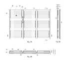
- FIG. 12is a diagrammatic sketch in a plan view showing a portion of the front (active) side of a semiconductor wafer having integrated circuit chip regions.
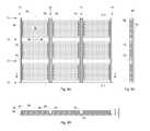
- FIGS. 13A and 14Aare diagrammatic sketches in a plan view showing singulated semiconductor die in a portion of an array formed by sawing a wafer as in FIG. 12 in a conventional manner illustrating die shift.
- FIGS. 13B and 14Bare diagrammatic sketches in a plan view showing the outline portions marked B in FIGS. 13A and 14A , respectively, enlarged.
- FIGS. 15A and 16Aare diagrammatic sketches in plan view each showing a portion of the front (active) side of a semiconductor wafer having integrated circuit chip regions.
- FIGS. 15B and 16Bare diagrammatic sketches in a plan view each showing a wafer array formed by performing a first wafer cutting procedure according to an embodiment of the invention, on a wafer as in FIGS. 15A and 16A , respectively.
- FIG. 12there is shown in a diagrammatic plan view a portion of a semiconductor wafer 120 , such as a silicon wafer, with the active side in view.
- a number of integrated circuit chipsare formed on the wafer, one of which is indicated at 12 B.
- An active region 120 of a chipis shown, bounded by saw streets 121 and 123 .
- Interconnect padsare arrayed in rows alongside opposite edges of the active region of the chip 120 and, accordingly, the chips shown by way of example in FIG. 12 (and other FIGs. herein) are peripheral-pad chips.
- FIGS. 13A , 14 Ashow singulated semiconductor die in a portion of an array resulting from sawing a wafer as in FIG. 12 in a conventional manner along streets 121 , 123 , illustrating die shift; and the portions marked “B” are enlarged in FIGS. 13B , 14 B, respectively.
- the die 130(and other die in a row between streets 131 ) has rotated; as a result the die sidewalls along the streets 133 and 131 are no longer parallel, so that the streets 133 and 131 are narrowed at some points and are no longer straight. Moreover, the interconnect pads on the rotated die are no longer arranged in the same pattern as in the uncut wafer.
- the die 140(and other die in a row between streets 141 , 141 ′) has been displaced (to the right in the FIGs.); as a result the street 141 is wider than in the uncut wafer; and street 141 ′ is narrower than in the uncut wafer. Moreover, the interconnect pads on the displaced die are no longer arranged in the same pattern as in the uncut wafer.
- an attempt to pass a cutting tool along the streetsmay result in damage to the shifted die.
- an attempt to address the interconnect pads using a mask or screen or an automated toolmay fail because the pads are no longer located in the expected positions.
- FIGS. 1A-6Billustrate embodiments in which a first wafer cutting procedure is carried out prior to thinning the wafer to the prescribed die thickness
- FIGS. 7A -11Billustrate an embodiment in which the wafer is thinned to the prescribed die thickness prior to carrying out a first wafer cutting procedure.
- cutsare performed along a set of streets to a depth at least as great as the prescribed die thickness; and, optionally, cuts are performed along another set of streets to a depth less than the prescribed die thickness.
- the result of the first cutting procedure and wafer thinningis an array of rows or blocks of die, where the rows or blocks are separated from one another, while the die within each row or block remain connected by the uncut portion of the wafer in the set of streets that were not cut or were cut to a depth less than the die thickness.
- the rows or blocks of dieare less subject to shift than singulated die would be, primarily in part because they have a greater area of contact with the underlying wafer support.
- One or more die preparation procedurescan then be carried out on the array of rows or blocks of die. Thereafter, the die are singulated by carrying out a second wafer cutting procedure along the second set of streets, passing completely through the thinned wafer array.
- the die preparation procedure that is carried out following the first cutting procedurerequires access to selected die edges or die sidewalls.
- the first set of streetsincludes the streets that are fronted by interconnect die edges.
- the die preparation procedure that is carried out following the first cutting procedureincludes an operation relating to features on the die, for example the die pads.
- a previously applied passivation layermay cover the die pads, and for subsequent electrical connection at the pads it is necessary to selectively remove the passivation layer over the pads to reveal the pad surface for electrical contact.
- FIG. 1Athere is shown in a diagrammatic plan view a portion of a semiconductor wafer 10 , such as a silicon wafer, with the active side in view.
- a semiconductor wafer 10such as a silicon wafer
- a number of integrated circuit chipsare formed on the wafer.
- An active region 12 of a chipis shown, bounded by saw streets 11 and 13 .
- Interconnect pads 18are arrayed alongside edges of the active region of the chip 12 and, accordingly, the chips shown by way of example in this FIG. (and other FIGs. herein) are peripheral-pad chips.
- the padsmay be located in this manner in the wafer as provided (that is, the original die pads may be suitably arranged peripheral pads); or, rerouting circuitry may connect pads on the wafer as provided to the desired peripheral interconnect locations.
- the interconnect pads 18are arranged in rows near two opposite edges 15 of each chip (e.g., rows 18 of pads 16 ), and these edges may be referred to for convenience as “interconnect edges”.
- the region 12 of the active side of the die adjacent the interconnect edges, in which the rows 16 of interconnect pads 18 are arranged,may be referred to for convenience as the “interconnect margins”. Certain of the saw streets in the wafer are fronted by the interconnect edges or margins.
- the streets that are fronted by the interconnect edges or margins(e.g., streets 11 ) all run parallel in one direction, and the streets not fronted by interconnect edges or margins (e.g., streets 13 ) run parallel in another direction, perpendicular to the first.
- the streets 11 fronted by interconnect edges or marginsmay be referred to for convenience as “N-S streets”, and the other streets 13 may be referred to for convenience as “E-W streets”.
- the designations “N-S” and “E-W” hereinare arbitrary and are made for convenient reference, and are not related to any particular view of the wafer.
- the wafer 10is mounted on a support 19 (a saw chuck, for example) associated with the wafer processing apparatus; at this stage the wafer is mounted with the front side facing away from the support.
- a dicing tape in a dicing framemay be placed on the saw chuck, and the wafer may be mounted on the dicing tape; but a tape is not required at this stage, and the wafer may be placed directly on the saw chuck.
- the wafer as providedhas a thickness w, which is greater (typically many times greater) than the eventual die thickness d.
- the wafer as providedmay have any thickness; a typical wafer may have a nominal thickness about 30 mils, or about 760 ⁇ m.
- the finished diemay in some embodiments have a thickness in a range about 20 ⁇ m to about 250 ⁇ m; and the depth of the trenches will be determined according to the desired finished die thickness.
- the finished diemay have a “standard” thickness, in a range about 120 ⁇ m to about 250 ⁇ m; or it may be “thin”, having a thickness in a range about 80 ⁇ m to about 120 ⁇ m; or it may be “ultra thin”, having a thickness in a range about 20 ⁇ m to about 80 ⁇ m.
- FIGS. 2A , 2 B, 2 Cillustrate the result of cutting along a first set of streets 11 (here, the N-S streets) to form parallel trenches 21 in the front side of the wafer to a depth s in the wafer greater than the eventual die thickness d.
- the trenchesdefine strips, defined by sidewalls 25 , each strip including a row of connected die 22 . At this stage the strips are connected by the wafer material remaining at the floor of the trenches 21 .
- FIGS. 3A , 3 B, 3 Cillustrate the result of (optionally) cutting along a second set of streets 13 (here, the E-W streets) to form parallel trenches 33 in the front side of the wafer to a depth in the wafer less than the eventual die thickness.
- the depth of the shallow cut along the second set of streetsmay be much less than the eventual die thickness and, in some examples the shallow cut may be nearly zero.
- the shallow cutdefines noninterconnect die edges, at least, and may define partial die noninterconnect sidewalls 37 .
- the first part and the second part (if employed) of the first wafer cutting proceduremay be carried out in any order; that is, the second part may be carried out prior to the first cut, or the first part may be carried out prior to the second part; and not all the cuts along one set of streets need be completed before cuts are completed along the other set of streets.
- This shallow cut part of the first cutting proceduremay be omitted altogether.
- a standard wafermay have a thickness about 29 mil and, where a die thickness of 50 ⁇ m is desired, the streets fronted by interconnect margins may be cut to a depth about 65 ⁇ m (about 15 ⁇ m deeper than the eventual die thickness), and the other streets may be cut to a depth nominally about 15 ⁇ m, defining die edges along those streets.
- a support 49such as a backgrinding tape is applied to the front side of the wafer and, if a dicing tape was used earlier, the dicing tape is removed to expose the back side of the wafer. Then the wafer is thinned, for example by backgrinding, to the eventual die thickness.
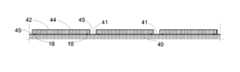
- a resulting constructis shown in FIGS. 4A , 4 B, 4 C. Because the trenches 21 along the N-S streets were in this example formed to a depth greater than the die thickness, thinning the wafer results in removal of the material remaining in these trenches, so that the result is an array of fully separated parallel strips 44 defined by sidewalls (here, interconnect die sidewalls) 45 and including a row of die 42 .
- An area 41 of the underlying support 49is exposed between the sidewalls (here, interconnect die sidewalls) 45 that were earlier defined by the deep trenches 21 .
- Some wafer material 43remains in the second set of streets (here, the E-W streets), because the shallower cut (even where it was carried out) is not deep enough to be exposed by the wafer thinning operation.
- the arrayis mounted on a support such as a backing tape, and the backgrinding tape is removed to expose the front side of the array of thinned and separated strips.
- a resultis shown in FIGS. 5A , 5 B, 5 C.
- the backside 42 of the strips 54is applied to the support 59 . Areas 51 of the support 59 are exposed between the strips 54 .
- Each stripincludes a row of die 52 , which are connected by the remaining portions 43 of wafer material in the streets 13 .
- a die preparation procedurecan now be carried out on exposed parts of the array; particularly, any of a variety of procedures can be carried out on features on the front side of the die (such as the interconnect pads), and/or any of a variety of procedures can be carried out on the sidewalls 55 or in the spaces between the strips. For instance, if a die attach film has earlier been applied to the backside of the wafer or the array, the film (not shown in these FIGs.) may be cut by passing a cutting tool (somewhat narrower than the tool employed in the first cutting procedure) through the space defined by the sidewalls 55 between the strips.
- the insulating layermay be selectively opened over die pads, to reveal the pad surfaces for later electrical connection; and, the insulating layer between the strips can be removed by passing a cutting tool (somewhat narrower than the tool employed in the first cutting procedure) through the space defined by the sidewalls 55 between the strips.
- the shallow cut part of the first cutting procedure(and the resulting stage shown in FIGS. 3A , 3 B, 3 C) may be omitted altogether.
- the array resulting from cutting the wafer along the first set of streets, as shown for example in FIGS. 2A , 2 B, 2 Ccan be thinned as follows.
- a support 49such as a backgrinding tape is applied to the front side of the wafer and the dicing tape is removed to expose the back side of the wafer. Then the wafer is thinned, for example by backgrinding, to the eventual die thickness.
- a resulting constructis shown in FIGS. 4D , 4 E, 4 F.
- the trenches 21 along the N-S streetswere in this example formed to a depth greater than the die thickness, thinning the wafer results in removal of the material remaining in these trenches, so that the result is an array of fully separated parallel strips 414 defined by sidewalls (here, interconnect die sidewalls) 415 and including a row of die 412 .
- An area 41 of the underlying support 49is exposed between the sidewalls (here, interconnect die sidewalls) 415 that were earlier defined by the deep trenches 21 .
- the second set of streets 413(here, the E-W streets), are not cut through, because the shallower cut (even where it was carried out) is not deep enough to be exposed by the wafer thinning operation.
- a tapesuch as a dicing tape is placed onto the back side of the wafer array.
- a die attach filmis placed onto the back side of the wafer array, and then the tape (dicing tape) is placed on the die attach film.
- the backgrind tapeis then removed to expose the front side of the array of thinned and separated strips.
- FIGS. 5D , 5 E, 5 FA result, where the shallow cut part of the first cutting procedure is omitted, is shown in FIGS. 5D , 5 E, 5 F.
- the backside 412 of the strips 514is applied to the support 59 . Areas 51 of the support 59 are exposed between the strips 514 .
- Each stripincludes a row of die 512 , which are connected by the wafer material 413 in the streets 13 .
- a die preparation procedurecan now be carried out on exposed parts of the array; particularly, any of a variety of procedures can be carried out on features on the front side of the die (such as the interconnect pads), and/or any of a variety of procedures can be carried out on the sidewalls 515 or in the spaces between the strips. For instance, if a die attach film has earlier been applied to the backside of the wafer or the array, the film (not shown in these FIGs.) may be cut by passing a cutting tool (somewhat narrower than the tool employed in the first cutting procedure) through the space defined by the sidewalls 515 between the strips.
- the insulating layermay be selectively opened over die pads, to reveal the pad surfaces for later electrical connection; and, the insulating layer between the strips can be removed by passing a cutting tool (somewhat narrower than the tool employed in the first cutting procedure) through the space defined by the sidewalls 515 between the strips.
- die preparation proceduresthat might advantageously be made prior to performing a second wafer cutting procedure are contemplated. These include, for example, mass formation of bumps on die interconnect pads, for example by screen printing; or formation of an under bump metallization on interconnect pads. Where the die preparation procedure requires heating, a heat-resistant tape may be used to support the array.
- singulation of the dieis completed in a second cutting procedure, in which the wafer is cut through (either from the front or the backside of the array) to remove wafer material remaining along the second set of streets between the die.
- a resulting array of singulated dieis shown in FIGS. 6A , 6 B, 6 C.
- the die 62are defined by sidewalls 67 (here, noninterconnect sidewalls) and by sidewalls 65 (here, interconnect sidewalls). Areas 63 of the support 69 , and areas 61 of the support 69 , are revealed in the second set of streets between the die 62 .
- the singulated diemay be further processed in the array, or they can be removed from the support and manipulated using a pick-and-place tool.
- FIGS. 7A through 11Cshow stages in an embodiment in which the wafer is thinned to the prescribed die thickness prior to carrying out a first wafer cutting procedure.
- the stagesinclude: mounting the wafer on a support, such as a backgrind tape applied to the front side of the wafer, and thinning the wafer to the desired die thickness ( FIGS. 7A , 7 B, 7 C); mounting the thinned wafer on a support such as a dicing tape applied to the backside of the thinned wafer, and removing the backgrinding tape to reveal the front side of the thinned wafer ( FIGS.
- a first cutting procedurewhich includes cutting through to (and slightly into) the support (that is, to a depth s 1 at least as great as the die thickness d) in a first set of streets (here, the N-S streets) ( FIGS. 9A , 9 B, 9 C) and (optionally) cutting into the wafer to a depth s 2 that is less than (and may be significantly less than) the die thickness d) ( FIGS. 10A , 10 B, 10 C).
- the result at this stageis an array of strips separated from one another by the trenches formed by the first cutting procedure in the first set of streets (the N-S streets), in which each strip includes a row of die attached (or partly attached) by wafer material remaining in the second set of streets.
- FIGS. 7A , 7 B, 7 Cshow a portion 70 of a wafer mounted onto a support 79 such as a backgrind tape applied to the front side of the wafer, and thinned (for example by backgrinding) to the eventual die thickness d.
- the die 72are bounded by saw streets 11 and 13 ; which contain the uncut wafer material 71 , 73 , respectively.
- the backside of the thinned waferis in view in FIG. 7A , and the active sides of the die 72 , including the interconnect pads 18 , face the support 79 .
- FIGS. 8A , 8 B, 8 Cshow the result of mounting the thinned wafer on a support such as a dicing tape applied to the backside of the thinned wafer, and removing the backgrinding tape to reveal the front side of the thinned wafer.
- FIGS. 9A , 9 B, 9 C, 10 A, 10 B and 10 Cshow the result of a first wafer cutting procedure, in which the wafer is cut (for example by cutting using a dicing saw) along a first set of streets and, optionally, along a second set of streets.
- FIGS. 9A , 9 B, 9 Cillustrate the result of cutting along a first set of streets 11 (here designated the N-S streets) to form parallel trenches 91 in the front side of the wafer to a depth s 1 at least as great as the eventual die thickness d. Because the wafer had earlier been thinned to the eventual die thickness d, the trenches extend through the wafer and to or into the support 79 .
- the trenchesdefine strips, defined by sidewalls 95 , each strip including a row 94 of connected die 92 . At this stage the strips are separated from one another, and the die 92 are fully connected by the wafer material remaining in the streets 13 .
- FIGS. 10A , 10 B, 10 Cillustrate the result of (optionally) cutting along a second set of streets 13 (here designated the E-W streets) to form parallel trenches 103 in the front side of the wafer to a depth s 2 in the wafer less than the eventual die thickness d.
- the depth of the shallow cut along the second set of streetsmay be much less than the eventual die thickness and, in some examples the shallow cut may be nearly zero.
- the shallow cutdefines noninterconnect die edges of the die 102 at least, and may define die noninterconnect partial sidewalls 107 .
- the first wafer cutting proceduremay be carried out in phases: in one (“first”) phase the wafer is cut along a first set of streets to a depth at least as great as the die thickness, and in another (optional “second”) phase the wafer is cut along a second set of streets to a depth less than the die thickness.
- first phasethe wafer is cut along a first set of streets to a depth at least as great as the die thickness
- second phasethe wafer is cut along a second set of streets to a depth less than the die thickness.
- both phases of the first wafer cutting proceduremay be carried out in any order; that is, the optional second phase may be carried out prior to the first phase, or the first phase may be carried out prior to the optional second phase; and not all the cuts along one set of streets need be completed before cuts are completed along the other set of streets.
- the second phasemay be omitted.
- a die preparation procedurecan now be carried out on exposed parts of the array, as described above; particularly, for example, any of a variety of procedures can be carried out on features on the front side of the die (such as the interconnect pads), and/or any of a variety of procedures can be carried out on the sidewalls or in the spaces between the strips. Examples are given above.
- the diemay be singulated by cutting through the wafer to a depth s 3 at least as great as the die thickness d in the second set of streets (here, the E-W streets) ( FIGS. 11A , 11 B, 11 C). Because the wafer had earlier been thinned to the eventual die thickness d, the trenches extend through the wafer and to or into the support 79 , as shown at 113 .
- the singulated die 112may be further processed in the array, or they can be removed from the support and manipulated using a pick-and-place tool.
- the diehave interconnect pads arrayed in rows alongside two opposite edges of the active region; that is, each die has two opposite interconnect edges.
- the diemay have interconnect pads arrayed alongside only one edge; that is, each die may have only one interconnect edge.
- the diemay have interconnect pads arrayed alongside two adjacent edges; that is, each die may have two interconnect edges that meet at a corner of the die.
- the padsmay be located in this manner in the wafer as provided (that is, the original die pads may be suitably arranged peripheral pads); or, rerouting circuitry may connect pads on the wafer as provided to the desired peripheral interconnect locations.
- FIG. 15Ashows a portion 150 of a wafer on which each die has one interconnect edge.
- the active regions of the dieare bounded by saw streets 151 , 151 ′ running parallel in one direction, and by saw streets 153 , running parallel in another direction, perpendicular to the first.
- the streets 151 , 151 ′may be referred to for convenience as “N-S streets” and the streets 153 may be referred to for convenience as “E-W streets”.
- Interconnect pads 158are arrayed in a row 156 along an edge of the active region of each die 152 defining interconnect edge 155 ; and interconnect pads 158 ′ are arrayed in a row 156 ′ along an edge of the active region of each die 152 ′, defining interconnect edge 155 ′.
- the respective interconnect edges of neighboring die 152 , 152 ′face in opposite directions; accordingly, streets 151 ′ are fronted on both sides by interconnect edges 155 ′, and streets 151 and 153 are fronted by non-interconnect edges.
- a first cutting proceduremay be carried out in streets 151 ′, and alternating parallel streets 151 are left uncut.
- the streets 151 ′constitute a first set of streets, and the remaining streets constitute a second set of streets.
- a resultis shown in FIG. 15B .
- the first cutting procedureforms parallel trenches in the front side of the wafer to a depth greater than the eventual die thickness.
- the trenchesdefine strips 157 , defined by interconnect sidewalls 159 , each strip including two rows of connected die 152 , 152 ′.
- the trenchespass through the thinned wafer to (and to some extent into) the wafer support, and the first cutting procedure results in an array of fully separated parallel strips.
- the result of thinningis an array of fully separated parallel strips 157 . Strips containing two rows of connected die are wider than strips containing only one row of connected die, and they therefore have a greater area of contact with the support. Strips having a greater area of contact with the support may be less likely to shift during a subsequent operation on the array.
- the first cutting proceduremay be complete at this stage; or, as in the foregoing examples, a shallower cut may optionally be made along some or all of the remaining streets. Die singulation results from carrying out a second cutting procedure, to remove wafer material remaining along the remaining streets.
- FIG. 16Ashows a portion 160 of a wafer on which each die has two adjacent interconnect edges, that is, on two edges that meet on each die at a corner of the die.
- the active regions of the dieare bounded by saw streets 161 , 161 ′ running parallel in one direction, and by saw streets 163 , 163 ′ running parallel in another direction, perpendicular to the first.
- the streets 161 , 161 ′may be referred to for convenience as “N-S streets” and the streets 163 , 163 ′ may be referred to for convenience as “E-W streets”.
- Interconnect pads 168are arrayed in a row 166 along an edge of the active region of each die 162 , 162 ′′, defining interconnect edges 165 ; and, similarly, interconnect pads are arrayed in a row 166 ′ along an edge of the active region of each die 162 ′, 162 ′′′ defining interconnect edges 165 ′.
- Interconnect pads 178are arrayed in a row 176 along an edge of the active region of each die 162 , 162 ′ defining interconnect edges 175 ; and, similarly, interconnect pads are arrayed in a row 176 ′ along an edge of the active region of each die 162 ′′, 162 ′′′ defining interconnect edge 175 ′.
- each diehas an interconnect edge fronting a N-S street 161 ′ and an interconnect edge fronting an E-W street 163 ′.
- the respective interconnect edges 165 , 165 ′, of neighboring die 162 , 162 ′face in opposite directions
- the respective interconnect edges 175 , 175 ′ of neighboring die 162 , 162 ′′face in opposite directions; accordingly, streets 161 ′, 163 ′ are fronted on both sides by interconnect edges, and streets 161 and 163 are fronted by non-interconnect edges.
- a first cutting proceduremay be carried out in streets 161 ′, 163 ′, and alternating parallel streets, respectively 161 , 163 , are left uncut or are only partially cut.
- the streets 161 ′, 163 ′constitute a first set of streets, and the remaining streets constitute a second set of streets.
- a resultis shown in FIG. 16B .
- the first cutting procedureforms parallel trenches in perpendicular directions in the front side of the wafer to a depth greater than the eventual die thickness.
- the trenchesdefine blocks 167 , defined by interconnect sidewalls 165 , 165 ′ and 175 , 175 ′, each block including four connected die 162 , 162 ′, 162 ′′, 162 ′′′.
- the trenchespass through the thinned wafer to (and to some extent into) the wafer support, and the first cutting procedure results in an array of fully separated blocks.
- the result of thinningis an array of fully separated blocks 167 .
- Blocks containing four connected diehave a greater area of contact with the support than a single die, and blocks having a greater area of contact with the support may be less likely to shift during a subsequent operation on the array.
- the first cutting proceduremay be complete at this stage; or, as in the foregoing examples, a shallower cut may optionally be made along some or all of the remaining streets. Die singulation results from carrying out a second cutting procedure, to remove wafer material remaining along the remaining streets.
- the following exampleillustrates in detail steps in a die separation process in which at least some die surfaces have an electrically insulative polymer coating, and the die are provided with a die attach film.
- the processbegins with a semiconductor wafer, containing semiconductor circuitry defining active die regions bounded by saw streets.
- Each active die regionhas interconnect pads situated along at least one edge (an “interconnect edge”).
- the padsmay be so situated in the wafer as provided from the fab; or, rerouting circuitry may be formed on the wafer as provided, to connect the original die pads to interconnect pads situated along one or more interconnect edges.
- the die in the wafer as providedmay be center pad die.
- the padsmay not be suitably arranged for the end use: the pads may not be situated on the desired interconnect edge; or the pads may be situated too close together for the desired interconnect technique.
- the first cutting procedureincludes a first part, in which cuts are made in a first set of streets which are fronted by interconnect die edges, from the front side of the wafer to a depth at least as great as the eventual die thickness. It may be advantageous to take some care in selecting cutting parameters, particularly the cut width and the cut depth.
- the saw kerfmust be narrower than the street width.
- the cut widthis a process parameter, and where it is desirable to have the die pads close to the resulting die edge, the cut should be made as wide as possible, but not so wide that the cut may damage the die seal at the die edges.
- the street widthis determined by specification or by direct measurement, and a narrower saw blade is selected; according to one standard rule, the blade width is preferably about 35 ⁇ m less than the street width, and is preferably at least about equal to and usually greater than half the street width.
- a blade providing a cut width at least 40 ⁇ m wide and less than 50 ⁇ mis selected;
- a “DF” blade, providing a cut width in the range 40-50 ⁇ m (nominally, 45 ⁇ m wide),may be suitable for this requirement.
- the trenches resulting from the cuts in the first set of streetsmust be deep enough so that the subsequent wafer thinning fully separates the strips or blocks of connected die; that is, the cut depth must be at least as great as the eventual die thickness.
- the cutis typically made to a depth about 50 ⁇ m deeper than the eventual die thickness; that is, for a 50 ⁇ m thick die, the cut would be made to a depth about 100 ⁇ m in the wafer (a 50 ⁇ m “overcut”).
- backgrindingcontinues through as much as 50 ⁇ m of the wafer after the trenches are encountered.
- the backgrinding toolimposes stresses on the wafer during the thinning procedure, and as soon as the trenches (or some of them) are encountered during backgrinding, these stresses may tend to force the resulting separated strips of blocks of die out of alignment. Accordingly, it may be advantageous to limit the backgrinding time to near the minimum required to encounter all the trenches and effect separation of all of the strips or blocks, to limit the amount of wafer material that must be ground away after all the trenches are encountered. This can be accomplished according to the invention by limiting the cut depth to near the eventual die thickness, that is, by limiting the overcut. The cut depth should exceed the eventual die thickness by only a small amount, to accommodate any variation in the actual cut and in the thickness of the wafer after backgrinding.
- Thismay be accomplished by programming the dicing saw to cut to a target depth only slightly deeper (such as 15 ⁇ m) than the die thickness. For example, for a desired die thickness about 50 ⁇ m, the saw may be set to cut to a depth about 65 ⁇ m (a 15 ⁇ m overcut).
- the cutting heightmay be indexed in any of a variety of ways.
- the sawis set to cut to a specified height above the cutting table.
- the cutting heightis determined by subtracting the desired cut depth from the overall thickness of the wafer plus dicing tape. Then the saw is set to cut to the cutting height.
- the total thickness of the wafer plus tapeis 870 ⁇ m; for a desired die thickness of 50 ⁇ m and a desired 50 ⁇ m overcut, the blade height is programmed to 770 ⁇ m over the cutting table.
- a 50 ⁇ m overcutis required when the cutting height is indexed to the cutting table, to compensate for greater variations in thickness; and a 15 ⁇ m overcut may not be reliably achievable using this conventional approach.
- the cut depthis indexed from the front side of the wafer, rather than from the cutting table.
- This capabilitymay be provided in programmable saws made by, for example, Disco Corporation (Japan).
- the waferis placed on the cutting table, and a test cut is made near the edge of the wafer.
- a noncontact devicesuch as one made by, for example, Keyence Corporation (Japan) is used to measure the depth of the test cut, to calibrate the apparatus.
- the sawis programmed to cut to the desired depth below the wafer front side surface.
- the apparatusmay be programmed to recalibrate at various intervals during the first cutting procedure (as frequently as following completion of the cut along each street, for example).
- the trenches formed by the cuts along streets fronted by interconnect edgesdefine interconnect sidewalls adjacent interconnect edges along which the die pads are arrayed.
- the front side of the die and the interconnect edges and sidewallsare thus made available for further treatment.
- a second part of the first cutting proceduremay be carried out, constituting making cuts along streets not fronted by interconnect edges, to a depth less than the eventual die thickness.
- a shallow trench depth about 15 ⁇ mmay be suitable.
- the resulting shallower trenchesdefine noninterconnect edges, and partial noninterconnect sidewalls, which are thus additionally made available for further treatment.
- a dicing tapemay protect the back side of the wafer array during subsequent treatment. If a dicing tape is desired, the wafer is mounted onto a dicing tape, and the dicing tape is mounted onto a film frame (for example, a dicing ring), prior to carrying out the first cutting procedure. Following the first cutting procedure, the dicing tape is cut between the outer edge of the wafer and the inner edge of the frame, to free the wafer from the film frame while leaving the dicing tape on the back side of the wafer.
- a film framefor example, a dicing ring
- features exposed on the wafer by the first cutting proceduremay be subject to a die preparation procedure.
- a parylene coatingis applied to all the exposed surfaces of the partially cut wafer.
- a standard parylene processis employed.
- the partially cut wafermay be plasma cleaned (for example, using an oxygen plasma), and an adhesion promoter may be applied to ensure good adhesion of the parylene to the surfaces.
- Suitable adhesion promotersinclude, for example, any of various “silane” adhesion promoters; a methacryloxy silane such as one marketed under the name “Silquest”, e.g., “Silquest A-174”.
- the partially cut waferpreferably having the back side protected by a tape (for example, a dicing tape) is placed in the parylene chamber, and parylene is deposited on all the exposed surfaces, including the front side, the walls and floors of the deeper trenches, and the walls and sides of the optional shallower trenches (if present).
- the parylene deposition processresults in a generally uniform conformal coating on all exposed surfaces.
- the thickness of the resulting coatingcan be controlled by, for example, controlling the process time.
- the parylene processis carried out to provide a continuous coating, preferably free of pinholes. In various examples various parylene thicknesses have been used; a coating of parylene C having a thickness about 2.5 ⁇ m may suffice, for example. In other examples coating thicknesses about 10 ⁇ m have been used.
- Thicker parylene coatingsmay be torn by a saw cut made following parylene deposition.
- the protective value of the parylenemay be compromised by a tear in the coating near a die edge. Tears at the floor of a trench may not have a detrimental effect and, accordingly, where such a thicker parylene coating is used, cutting to form shallower trenches may be advantageous.
- thinner parylene coatingssuch as 2.5 ⁇ m are less likely to be torn by the saw cut and, where a thinner parylene coating is used, a second phase of the first cutting procedure may be unnecessary.
- the parylene processresults in deposition of parylene on all exposed surfaces, and the parylene precursor molecules can invade very thin spaces. Parylene on the back side of the wafer can interfere with a subsequent backgrinding process, by loading the grinding wheel. Accordingly, it may be advantageous to protect the back side of the wafer (for example, by leaving a tape in place until the parylene process is complete), so that no parylene forms there. After the parylene process has been completed, the dicing tape (where present) may be removed from the back side of the wafer.
- One or more additional die preparation proceduresmay be carried out. Particularly, where, as in this example, interconnect pads are obscured by the parylene coating on all the exposed surfaces of the partially cut wafer, the pads at which electrical interconnection of the die is to be made must be exposed.
- a particularly suitable technique for exposing padsis laser ablation, and this can advantageously be carried out at a wafer array stage, before the die have been singulated, so that the die have not shifted and the die (and the pads) are properly aligned.
- the laser apparatuscan be set up and aligned, and then robotically stepped from pad to pad and from die to die.
- a wafer thinning procedurecan be conducted, for example by backgrinding using selected grinding wheels (cups, discs).
- the waferis mounted onto a grinding tape, by applying the tape to the (parylene coated, in this example) front side of the wafer. Once the dicing tape (where one was used) has been removed, the back side of the wafer is exposed for backgrinding.
- the protocol in this exampleis directed to minimizing mechanical impact of the grinding wheel on the wafer and on the wafer array during the thinning operation, to minimize shifting of the strips or blocks, or die, in the array and to minimize propagation of stress through the wafer. It may be preferred to carry out the thinning procedure in stages: in this example a first stage employs a coarse grinding wheel (for example a 320 grit); a second stage employs a finer vitrified grinding wheel (for example a vitrified 4800 grit); and a third stage employs a polishing wheel.
- a vitrified (vitreous inorganic fiber) wheelis available from, for example, Disco Corporation (Japan). Separation of the strips or blocks of die occurs during the second stage, when mechanical impact is reduced by use of the vitrified wheel.
- a die attach filmis applied to the polished back side of the thinned wafer.
- Preferred die attach filmsinclude films available from Hitachi (e.g., FH 900) or from Nitto (e.g., EM 500, EM 700), for example, and the film may be permitted to “set” for a time (for example at least about 4 hours) to ensure reliable adhesion to the wafer array and, particularly, to minimize die shift during removal of the grinding tape from the front side.
- the grinding tapeis removed by peeling it away.
- the tapeis peeled from the die in a corner-to-corner direction, for example in a direction at about a 45° angle with respect to the die edges.
- the tapeis preferably removed by peeling in a direction parallel to the interconnect edge streets (or, for die blocks, parallel to longer interconnect edges), to minimize sideways stresses on the strips or blocks.
- the die attach filmis cut in the deep trenches fronted by interconnect edges. Because array shift has been minimized, the die attach film cut can confidently be made without damaging the die or the parylene film (where present) on the interconnect die sidewalls. Where a saw is used for this cut the saw must be narrow enough so that it does not impact the die or the parylene film (where present) on the interconnect sidewalls. As may be appreciated, thicker parylene films will occupy a greater portion of the street width, and this will require a thinner saw. Also, it may be advantageous to refine the control of the saw for the die attach film cut.
- the sawIn a conventional saw procedure, the saw is aligned for a first cut, and is thereafter stepped across the wafer from street to street, relying for proper alignment on the specified step interval.
- the sawmay be realigned/recalibrated before cutting at selected ones or all of the streets using fiducials associated with each street.
- a number of measurementsmay be made in or on the street, and the data may be treated statistically to determine a best saw path for the street.
- a second wafer cutting procedureis carried out, to cut all the way through the wafer material remaining in the streets not fronted by interconnect die edges, and through the die attach film below these streets, resulting in singulated die.
- the singulated die arrayis now ready for further treatment, including for example, removal and placement using a pick-and-place tool.
Landscapes
- Engineering & Computer Science (AREA)
- Computer Hardware Design (AREA)
- Microelectronics & Electronic Packaging (AREA)
- Power Engineering (AREA)
- Manufacturing & Machinery (AREA)
- Physics & Mathematics (AREA)
- Condensed Matter Physics & Semiconductors (AREA)
- General Physics & Mathematics (AREA)
- Dicing (AREA)
- Mechanical Treatment Of Semiconductor (AREA)
Abstract
Description
Claims (8)
Priority Applications (1)
| Application Number | Priority Date | Filing Date | Title |
|---|---|---|---|
| US12/982,376US8884403B2 (en) | 2008-06-19 | 2010-12-30 | Semiconductor die array structure |
Applications Claiming Priority (3)
| Application Number | Priority Date | Filing Date | Title |
|---|---|---|---|
| US13270808P | 2008-06-19 | 2008-06-19 | |
| US12/323,288US7863159B2 (en) | 2008-06-19 | 2008-11-25 | Semiconductor die separation method |
| US12/982,376US8884403B2 (en) | 2008-06-19 | 2010-12-30 | Semiconductor die array structure |
Related Parent Applications (1)
| Application Number | Title | Priority Date | Filing Date |
|---|---|---|---|
| US12/323,288DivisionUS7863159B2 (en) | 2008-05-20 | 2008-11-25 | Semiconductor die separation method |
Publications (2)
| Publication Number | Publication Date |
|---|---|
| US20110101505A1 US20110101505A1 (en) | 2011-05-05 |
| US8884403B2true US8884403B2 (en) | 2014-11-11 |
Family
ID=41430362
Family Applications (2)
| Application Number | Title | Priority Date | Filing Date |
|---|---|---|---|
| US12/323,288Expired - Fee RelatedUS7863159B2 (en) | 2008-05-20 | 2008-11-25 | Semiconductor die separation method |
| US12/982,376ActiveUS8884403B2 (en) | 2008-06-19 | 2010-12-30 | Semiconductor die array structure |
Family Applications Before (1)
| Application Number | Title | Priority Date | Filing Date |
|---|---|---|---|
| US12/323,288Expired - Fee RelatedUS7863159B2 (en) | 2008-05-20 | 2008-11-25 | Semiconductor die separation method |
Country Status (5)
| Country | Link |
|---|---|
| US (2) | US7863159B2 (en) |
| JP (1) | JP2011525055A (en) |
| KR (1) | KR101609004B1 (en) |
| TW (1) | TWI479553B (en) |
| WO (1) | WO2009155247A2 (en) |
Cited By (1)
| Publication number | Priority date | Publication date | Assignee | Title |
|---|---|---|---|---|
| US20150279786A1 (en)* | 2014-04-01 | 2015-10-01 | Seiko Instruments Inc. | Semiconductor wafer |
Families Citing this family (20)
| Publication number | Priority date | Publication date | Assignee | Title |
|---|---|---|---|---|
| WO2008157722A1 (en)* | 2007-06-19 | 2008-12-24 | Vertical Circuits, Inc. | Wafer level surface passivation of stackable integrated circuit chips |
| WO2009035849A2 (en) | 2007-09-10 | 2009-03-19 | Vertical Circuits, Inc. | Semiconductor die mount by conformal die coating |
| CN101999167B (en) | 2008-03-12 | 2013-07-17 | 伊文萨思公司 | Support mounted electrically interconnected die assembly |
| US9153517B2 (en) | 2008-05-20 | 2015-10-06 | Invensas Corporation | Electrical connector between die pad and z-interconnect for stacked die assemblies |
| WO2011056668A2 (en) | 2009-10-27 | 2011-05-12 | Vertical Circuits, Inc. | Selective die electrical insulation additive process |
| US8587088B2 (en) | 2011-02-17 | 2013-11-19 | Apple Inc. | Side-mounted controller and methods for making the same |
| JP2012195388A (en)* | 2011-03-15 | 2012-10-11 | Toshiba Corp | Semiconductor device manufacturing method and semiconductor device |
| TWI450325B (en)* | 2012-03-22 | 2014-08-21 | Alpha & Omega Semiconductor | A method for encapsulating wafer which support wafer backside sawing |
| US8975162B2 (en)* | 2012-12-20 | 2015-03-10 | Applied Materials, Inc. | Wafer dicing from wafer backside |
| WO2015063655A1 (en)* | 2013-10-29 | 2015-05-07 | Koninklijke Philips N.V. | Separating a wafer of light emitting devices |
| KR102306517B1 (en)* | 2013-10-29 | 2021-10-01 | 루미리즈 홀딩 비.브이. | Separating a wafer of light emitting devices |
| US9871019B2 (en) | 2015-07-17 | 2018-01-16 | Invensas Corporation | Flipped die stack assemblies with leadframe interconnects |
| US9490195B1 (en) | 2015-07-17 | 2016-11-08 | Invensas Corporation | Wafer-level flipped die stacks with leadframes or metal foil interconnects |
| US9825002B2 (en) | 2015-07-17 | 2017-11-21 | Invensas Corporation | Flipped die stack |
| US9508691B1 (en) | 2015-12-16 | 2016-11-29 | Invensas Corporation | Flipped die stacks with multiple rows of leadframe interconnects |
| US10566310B2 (en) | 2016-04-11 | 2020-02-18 | Invensas Corporation | Microelectronic packages having stacked die and wire bond interconnects |
| US9595511B1 (en) | 2016-05-12 | 2017-03-14 | Invensas Corporation | Microelectronic packages and assemblies with improved flyby signaling operation |
| US9728524B1 (en) | 2016-06-30 | 2017-08-08 | Invensas Corporation | Enhanced density assembly having microelectronic packages mounted at substantial angle to board |
| JP2018074083A (en)* | 2016-11-02 | 2018-05-10 | 株式会社ディスコ | Processing method of wafer |
| CN113053770B (en)* | 2021-03-15 | 2024-03-08 | 上海华力微电子有限公司 | Wafer cutting method |
Citations (206)
| Publication number | Priority date | Publication date | Assignee | Title |
|---|---|---|---|---|
| US4323914A (en) | 1979-02-01 | 1982-04-06 | International Business Machines Corporation | Heat transfer structure for integrated circuit package |
| US4336551A (en) | 1977-05-30 | 1982-06-22 | Hitachi, Ltd. | Thick-film printed circuit board and method for producing the same |
| US4363076A (en) | 1980-12-29 | 1982-12-07 | Honeywell Information Systems Inc. | Integrated circuit package |
| US4500905A (en) | 1981-09-30 | 1985-02-19 | Tokyo Shibaura Denki Kabushiki Kaisha | Stacked semiconductor device with sloping sides |
| US4784972A (en) | 1984-08-18 | 1988-11-15 | Matsushita Electric Industrial Co. Ltd. | Method of joining beam leads with projections to device electrodes |
| US5107325A (en) | 1989-04-17 | 1992-04-21 | Seiko Epson Corporation | Structure and method of packaging a semiconductor device |
| US5138438A (en) | 1987-06-24 | 1992-08-11 | Akita Electronics Co. Ltd. | Lead connections means for stacked tab packaged IC chips |
| US5200362A (en) | 1989-09-06 | 1993-04-06 | Motorola, Inc. | Method of attaching conductive traces to an encapsulated semiconductor die using a removable transfer film |
| US5218234A (en) | 1991-12-23 | 1993-06-08 | Motorola, Inc. | Semiconductor device with controlled spread polymeric underfill |
| US5311401A (en) | 1991-07-09 | 1994-05-10 | Hughes Aircraft Company | Stacked chip assembly and manufacturing method therefor |
| US5331591A (en) | 1993-02-01 | 1994-07-19 | At&T Bell Laboratories | Electronic module including a programmable memory |
| US5334872A (en) | 1990-01-29 | 1994-08-02 | Mitsubishi Denki Kabushiki Kaisha | Encapsulated semiconductor device having a hanging heat spreading plate electrically insulated from the die pad |
| FR2704690A1 (en) | 1993-04-27 | 1994-11-04 | Thomson Csf | Method for encapsulating semiconductor wafers, device obtained by this process and application to the interconnection of wafers in three dimensions. |
| US5434745A (en) | 1994-07-26 | 1995-07-18 | White Microelectronics Div. Of Bowmar Instrument Corp. | Stacked silicon die carrier assembly |
| US5466634A (en) | 1994-12-20 | 1995-11-14 | International Business Machines Corporation | Electronic modules with interconnected surface metallization layers and fabrication methods therefore |
| US5538758A (en) | 1995-10-27 | 1996-07-23 | Specialty Coating Systems, Inc. | Method and apparatus for the deposition of parylene AF4 onto semiconductor wafers |
| US5571754A (en) | 1995-07-26 | 1996-11-05 | International Business Machines Corporation | Method of fabrication of endcap chip with conductive, monolithic L-connect for multichip stack |
| US5616953A (en) | 1994-09-01 | 1997-04-01 | Micron Technology, Inc. | Lead frame surface finish enhancement |
| US5629566A (en) | 1994-08-15 | 1997-05-13 | Kabushiki Kaisha Toshiba | Flip-chip semiconductor devices having two encapsulants |
| US5691248A (en) | 1995-07-26 | 1997-11-25 | International Business Machines Corporation | Methods for precise definition of integrated circuit chip edges |
| US5698895A (en) | 1994-06-23 | 1997-12-16 | Cubic Memory, Inc. | Silicon segment programming method and apparatus |
| US5721151A (en)* | 1995-06-07 | 1998-02-24 | Lsi Logic Corporation | Method of fabricating a gate array integrated circuit including interconnectable macro-arrays |
| US5731631A (en) | 1996-02-01 | 1998-03-24 | Mitsubishi Denki Kabushiki Kaisha | Semiconductor device with tape automated bonding element |
| US5737191A (en) | 1995-04-07 | 1998-04-07 | Shinko Electric Industries Co., Ltd. | Structure and process for mounting semiconductor chip |
| US5870351A (en) | 1994-10-21 | 1999-02-09 | The Board Of Trustees Of The Leland Stanford Junior University | Broadband microfabriated ultrasonic transducer and method of fabrication |
| WO1999007015A1 (en) | 1997-07-29 | 1999-02-11 | Cubic Memory, Inc. | Conductive epoxy flip-chip on chip |
| WO1999009599A2 (en) | 1997-08-21 | 1999-02-25 | Cubic Memory, Inc. | Vertical interconnect process for silicon segments with dielectric isolation |
| KR19990008537U (en) | 1997-08-06 | 1999-03-05 | 전주범 | Drum motor mounting structure of head drum assembly |
| US5879965A (en) | 1997-06-19 | 1999-03-09 | Micron Technology, Inc. | Plastic lead frames for semiconductor devices, packages including same, and methods of fabrication |
| US5891761A (en) | 1994-06-23 | 1999-04-06 | Cubic Memory, Inc. | Method for forming vertical interconnect process for silicon segments with thermally conductive epoxy preform |
| US5910687A (en) | 1997-01-24 | 1999-06-08 | Chipscale, Inc. | Wafer fabrication of die-bottom contacts for electronic devices |
| US5946545A (en) | 1994-03-30 | 1999-08-31 | Internatinal Business Machines Corporation | Semiconductor stack structures and fabrication/sparing methods utilizing programmable spare circuit |
| JPH11260851A (en) | 1998-03-11 | 1999-09-24 | Matsushita Electric Ind Co Ltd | Semiconductor device and method of manufacturing the semiconductor device |
| US5965947A (en) | 1996-08-20 | 1999-10-12 | Samsung Electronics Co., Ltd. | Structure of a semiconductor package including chips bonded to die bonding pad with conductive adhesive and chips bonded with non-conductive adhesive containing insulating beads |
| US6030854A (en) | 1996-03-29 | 2000-02-29 | Intel Corporation | Method for producing a multilayer interconnection structure |
| US6034438A (en) | 1996-10-18 | 2000-03-07 | The Regents Of The University Of California | L-connect routing of die surface pads to the die edge for stacking in a 3D array |
| US6087716A (en) | 1997-02-03 | 2000-07-11 | Nec Corporation | Semiconductor device package having a connection substrate with turned back leads and method thereof |
| US6107164A (en) | 1998-08-18 | 2000-08-22 | Oki Electric Industry Co., Ltd. | Using grooves as alignment marks when dicing an encapsulated semiconductor wafer |
| JP2000269411A (en) | 1999-03-17 | 2000-09-29 | Shinko Electric Ind Co Ltd | Semiconductor device and manufacture thereof |
| EP1041624A1 (en) | 1999-04-02 | 2000-10-04 | Interuniversitair Microelektronica Centrum Vzw | Method of transferring ultra-thin substrates and application of the method to the manufacture of a multilayer thin film device |
| US6175158B1 (en) | 1998-09-08 | 2001-01-16 | Lucent Technologies Inc. | Interposer for recessed flip-chip package |
| US6228686B1 (en) | 1995-09-18 | 2001-05-08 | Tessera, Inc. | Method of fabricating a microelectronic assembly using sheets with gaps to define lead regions |
| US6255726B1 (en) | 1994-06-23 | 2001-07-03 | Cubic Memory, Inc. | Vertical interconnect process for silicon segments with dielectric isolation |
| KR20010062722A (en) | 1999-12-28 | 2001-07-07 | 루이스 에이. 헥트 | System for testing bare ic chips and a socket for such chips |
| US6262476B1 (en) | 1998-07-27 | 2001-07-17 | Siemens Aktiengesellschaft | Composite member composed of at least two integrated circuits and method for the manufacture of a composite member composed of at least two integrated circuits |
| JP2001210782A (en) | 2000-01-27 | 2001-08-03 | Seiko Epson Corp | Semiconductor chip, multi-chip package, semiconductor device, and electronic device using the same |
| WO2001064344A2 (en) | 2000-03-02 | 2001-09-07 | Microchips, Inc. | Microfabricated devices for the storage and selective exposure of chemicals and devices |
| US6297657B1 (en) | 1999-01-11 | 2001-10-02 | Wentworth Laboratories, Inc. | Temperature compensated vertical pin probing device |
| US6303977B1 (en) | 1998-12-03 | 2001-10-16 | Texas Instruments Incorporated | Fully hermetic semiconductor chip, including sealed edge sides |
| US20010031548A1 (en) | 1997-10-20 | 2001-10-18 | Peter Elenius | Method for forming chip scale package |
| US6315856B1 (en) | 1998-03-19 | 2001-11-13 | Kabushiki Kaisha Toshiba | Method of mounting electronic component |
| US6326244B1 (en) | 1998-09-03 | 2001-12-04 | Micron Technology, Inc. | Method of making a cavity ball grid array apparatus |
| US6326689B1 (en) | 1999-07-26 | 2001-12-04 | Stmicroelectronics, Inc. | Backside contact for touchchip |
| US6338980B1 (en) | 1999-08-13 | 2002-01-15 | Citizen Watch Co., Ltd. | Method for manufacturing chip-scale package and manufacturing IC chip |
| US20020006686A1 (en) | 2000-07-12 | 2002-01-17 | Cloud Eugene H. | Die to die connection method and assemblies and packages including dice so connected |
| US6351030B2 (en) | 1997-09-29 | 2002-02-26 | International Business Machines Corporation | Electronic package utilizing protective coating |
| US20020027257A1 (en) | 2000-06-02 | 2002-03-07 | Kinsman Larry D. | Method for fabricating a chip scale package using wafer level processing and devices resulting therefrom |
| US20020045290A1 (en) | 1996-02-20 | 2002-04-18 | Michael B. Ball | Flip chip and conventional stack |
| US20020096349A1 (en) | 2001-01-24 | 2002-07-25 | Harry Hedler | Electronic component with a semiconductor chip and method of producing the electronic component |
| US20020127775A1 (en) | 1999-12-23 | 2002-09-12 | Rambus Inc. | Redistributed bond pads in stacked integrated circuit die package |
| US6472746B2 (en) | 2000-08-02 | 2002-10-29 | Fujitsu Limited | Semiconductor device having bonding wires serving as external connection terminals |
| US6476467B2 (en) | 1997-01-31 | 2002-11-05 | Hitachi, Ltd. | Semiconductor device and process for producing the same |
| US20020168798A1 (en) | 1996-10-31 | 2002-11-14 | Glenn Thomas P. | Method of making near chip size integrated circuit package |
| US20020180010A1 (en) | 1996-11-21 | 2002-12-05 | Kunihiro Tsubosaki | Semiconductor device and manufacturing method thereof |
| US20020185725A1 (en) | 1998-08-21 | 2002-12-12 | Moden Walter L. | Low profile multi-IC chip package connector |
| US20020187260A1 (en) | 2001-05-30 | 2002-12-12 | Sheppard Norman F. | Conformal coated microchip reservoir devices |
| US20030038353A1 (en) | 2001-08-23 | 2003-02-27 | Derderian James M. | Assemblies including stacked semiconductor devices separated by discrete conductive elements therebetween, packages including the assemblies, and methods |
| US20030038357A1 (en) | 2001-08-24 | 2003-02-27 | Derderian James M. | Spacer for semiconductor devices, semiconductor devices and assemblies including the spacer, and methods |
| US20030038356A1 (en) | 2001-08-24 | 2003-02-27 | Derderian James M | Semiconductor devices including stacking spacers thereon, assemblies including the semiconductor devices, and methods |
| US20030071341A1 (en) | 2001-10-16 | 2003-04-17 | Jeung Boon Suan | Apparatus and method for leadless packaging of semiconductor devices |
| US20030092326A1 (en) | 2000-06-16 | 2003-05-15 | Hidenobu Nishikawa | Electronic parts packaging method and electronic parts package |
| JP2003142518A (en) | 2001-11-02 | 2003-05-16 | Nec Electronics Corp | Device and method for manufacturing semiconductor, semiconductor device, and electronic device |
| US20030096454A1 (en) | 2001-11-16 | 2003-05-22 | Poo Chia Yong | Stackable semiconductor package and wafer level fabrication method |
| US6569709B2 (en) | 2001-10-15 | 2003-05-27 | Micron Technology, Inc. | Assemblies including stacked semiconductor devices separated a distance defined by adhesive material interposed therebetween, packages including the assemblies, and methods |
| US20030099085A1 (en) | 2001-11-26 | 2003-05-29 | Delaware Capital Formation, Inc. | Surface flashover resistant capacitors and method for producing same |
| JP2003163324A (en) | 2001-11-27 | 2003-06-06 | Nec Corp | Unit semiconductor device and manufacturing method thereof, and three-dimensional laminated semiconductor device |
| USD475981S1 (en) | 2002-03-29 | 2003-06-17 | Mitsubishi Denki Kabushiki Kaisha | Integrated circuits substrate |
| US6580165B1 (en) | 2000-11-16 | 2003-06-17 | Fairchild Semiconductor Corporation | Flip chip with solder pre-plated leadframe including locating holes |
| US20030122243A1 (en) | 2001-12-31 | 2003-07-03 | Jin-Yuan Lee | Integrated chip package structure using organic substrate and method of manufacturing the same |
| US6593648B2 (en) | 2000-08-31 | 2003-07-15 | Seiko Epson Corporation | Semiconductor device and method of making the same, circuit board and electronic equipment |
| US6607941B2 (en) | 2002-01-11 | 2003-08-19 | National Semiconductor Corporation | Process and structure improvements to shellcase style packaging technology |
| US6607938B2 (en) | 2001-07-19 | 2003-08-19 | Samsung Electronics Co., Ltd. | Wafer level stack chip package and method for manufacturing same |
| US6621172B2 (en) | 1999-09-03 | 2003-09-16 | Seiko Epson Corporation | Semiconductor device and method of fabricating the same, circuit board, and electronic equipment |
| US6621155B1 (en) | 1999-12-23 | 2003-09-16 | Rambus Inc. | Integrated circuit device having stacked dies and impedance balanced transmission lines |
| US20030209772A1 (en) | 2002-05-13 | 2003-11-13 | National Semiconductor Corporation | Electrical die contact structure and fabrication method |
| US6656827B1 (en) | 2002-10-17 | 2003-12-02 | Taiwan Semiconductor Manufacturing Co., Ltd. | Electrical performance enhanced wafer level chip scale package with ground |
| US6667543B1 (en) | 2002-10-29 | 2003-12-23 | Motorola, Inc. | Optical sensor package |
| US6670701B2 (en) | 2001-02-01 | 2003-12-30 | Mitsubishi Denki Kabushiki Kaisha | Semiconductor module and electronic component |
| US6674159B1 (en) | 2000-05-16 | 2004-01-06 | Sandia National Laboratories | Bi-level microelectronic device package with an integral window |
| US6706971B2 (en) | 2001-01-26 | 2004-03-16 | Irvine Sensors Corporation | Stackable microcircuit layer formed from a plastic encapsulated microcircuit |
| JP2004119473A (en) | 2002-09-24 | 2004-04-15 | Seiko Epson Corp | Semiconductor device and its manufacturing method, circuit board, and electronic equipment |
| US6722213B2 (en) | 2000-02-06 | 2004-04-20 | Minitubes Gmbh | Temperature-adjusted sampler for fluids |
| US6737743B2 (en)* | 2001-07-10 | 2004-05-18 | Kabushiki Kaisha Toshiba | Memory chip and semiconductor device using the memory chip and manufacturing method of those |
| JP2004153130A (en) | 2002-10-31 | 2004-05-27 | Olympus Corp | Semiconductor device and its manufacturing method |
| JP2004158536A (en) | 2002-11-05 | 2004-06-03 | Fujitsu Ltd | Semiconductor device and method of manufacturing semiconductor device |
| US6750547B2 (en) | 2001-12-26 | 2004-06-15 | Micron Technology, Inc. | Multi-substrate microelectronic packages and methods for manufacture |
| US20040113283A1 (en) | 2002-03-06 | 2004-06-17 | Farnworth Warren M. | Method for fabricating encapsulated semiconductor components by etching |
| US6756252B2 (en) | 2002-07-17 | 2004-06-29 | Texas Instrument Incorporated | Multilayer laser trim interconnect method |
| JP2004214548A (en) | 2003-01-08 | 2004-07-29 | Mitsubishi Electric Corp | Component built-in board type module, board on which it is mounted, method of manufacturing component built-in board type module, and method of manufacturing board mounted with component built-in board type module |
| US20040150095A1 (en) | 2003-01-30 | 2004-08-05 | Endicott Interconnect Technologies, Inc. | Stacked chip electronic package having laminate carrier and method of making same |
| CN1531069A (en) | 2003-03-13 | 2004-09-22 | ������������ʽ���� | Electronic device and manufacturing method thereof |
| US20040195667A1 (en) | 2003-04-04 | 2004-10-07 | Chippac, Inc | Semiconductor multipackage module including processor and memory package assemblies |
| US20040198033A1 (en) | 2002-08-20 | 2004-10-07 | Lee Teck Kheng | Double bumping of flexible substrate for first and second level interconnects |
| US6802446B2 (en) | 2002-02-01 | 2004-10-12 | Delphi Technologies, Inc. | Conductive adhesive material with metallurgically-bonded conductive particles |
| US20040212083A1 (en) | 2000-09-21 | 2004-10-28 | Jicheng Yang | Method to prevent die attach adhesive contamination in stacked chips |
| US20040217446A1 (en) | 2003-01-02 | 2004-11-04 | Headley William R. | Method and apparatus for preparing a plurality of dice in wafers |
| TW200425356A (en) | 2002-12-09 | 2004-11-16 | Advanced Interconnect Tech Ltd | Package having exposed integrated circuit device |
| US20040238933A1 (en) | 2003-05-27 | 2004-12-02 | Shou-Lung Chen | Stacked package for electronic elements and packaging method thereof |
| US20040251520A1 (en) | 2003-06-10 | 2004-12-16 | Sanyo Electric Co., Ltd. | Method for manufacturing semiconductor device |
| US20040262035A1 (en) | 2003-06-30 | 2004-12-30 | Bing-Hong Ko | Electronic component mounting structure |
| JP2005005529A (en) | 2003-06-12 | 2005-01-06 | Toshiba Corp | 3D mounting semiconductor module and 3D mounting semiconductor system |
| US6844623B1 (en) | 2000-05-16 | 2005-01-18 | Sandia Corporation | Temporary coatings for protection of microelectronic devices during packaging |
| US20050013927A1 (en) | 2003-02-06 | 2005-01-20 | Semiconductor Energy Laboratory Co., Ltd. | Manufacturing method for display device |
| KR20050009036A (en) | 2003-07-15 | 2005-01-24 | 삼성전자주식회사 | Stack package and manufacturing method thereof |
| US6849802B2 (en) | 2002-02-06 | 2005-02-01 | Samsung Electronics Co., Ltd | Semiconductor chip, chip stack package and manufacturing method |
| US20050067680A1 (en) | 2003-09-30 | 2005-03-31 | Boon Suan Jeung | Castellated chip-scale packages and methods for fabricating the same |
| US20050067694A1 (en)* | 2003-09-30 | 2005-03-31 | Pon Florence R. | Spacerless die stacking |
| US20050082651A1 (en) | 2003-10-20 | 2005-04-21 | Farnworth Warren M. | Methods of coating and singulating wafers and chip-scale packages formed therefrom |
| US20050085050A1 (en) | 2003-10-21 | 2005-04-21 | Draney Nathan R. | Substrate thinning including planarization |
| US20050101039A1 (en) | 2002-10-30 | 2005-05-12 | John Chen | Apparatus and method for stacking laser bars for uniform facet coating |
| US20050104179A1 (en) | 2003-07-03 | 2005-05-19 | Shellcase Ltd. | Methods and apparatus for packaging integrated circuit devices |
| US6910268B2 (en) | 2001-03-27 | 2005-06-28 | Formfactor, Inc. | Method for fabricating an IC interconnect system including an in-street integrated circuit wafer via |
| TW200527549A (en) | 2004-02-05 | 2005-08-16 | United Microelectronics Corp | Ultra-thin wafer level stack packaging method and structure using thereof |
| DE102004039906A1 (en) | 2004-08-18 | 2005-08-18 | Infineon Technologies Ag | Electronic component with a number of integrated members, is formed by producing members with a surface that contains a circuit, and connecting components using bond wires |
| WO2005081315A2 (en) | 2004-02-18 | 2005-09-01 | Infineon Technologies Ag | Semiconductor component comprising a stack of semiconductor chips and method for producing the same |
| US6940022B1 (en) | 1997-12-18 | 2005-09-06 | Vlt, Inc. | Protective coating for an electronic device |
| US6956283B1 (en) | 2000-05-16 | 2005-10-18 | Peterson Kenneth A | Encapsulants for protecting MEMS devices during post-packaging release etch |
| US20050230802A1 (en) | 2004-04-13 | 2005-10-20 | Al Vindasius | Stacked die BGA or LGA component assembly |
| US20050248021A1 (en) | 2004-05-06 | 2005-11-10 | Henrik Morkner | Multi-mode integrated circuit structure |
| US20050258530A1 (en) | 2004-04-13 | 2005-11-24 | Al Vindasius | Micropede stacked die component assembly |
| US6972480B2 (en) | 2003-06-16 | 2005-12-06 | Shellcase Ltd. | Methods and apparatus for packaging integrated circuit devices |
| US20050287705A1 (en) | 2004-06-25 | 2005-12-29 | Advanced Semiconductor Engineering, Inc. | Flip chip on leadframe package and method for manufacturing the same |
| US20060003552A1 (en)* | 2004-07-01 | 2006-01-05 | Disco Corporation | Wafer dividing method |
| US6984885B1 (en) | 2000-02-10 | 2006-01-10 | Renesas Technology Corp. | Semiconductor device having densely stacked semiconductor chips |
| US20060055050A1 (en) | 2004-09-10 | 2006-03-16 | Hideo Numata | Semiconductor device and manufacturing method thereof |
| US20060068567A1 (en) | 2004-09-24 | 2006-03-30 | Eric Beyne | Method for chip singulation |
| US20060076690A1 (en) | 2004-09-27 | 2006-04-13 | Formfactor, Inc. | Stacked Die Module |
| US20060094165A1 (en) | 2004-10-29 | 2006-05-04 | Harry Hedler | Method for fabricating semiconductor components |
| US20060097356A1 (en)* | 2004-11-11 | 2006-05-11 | Fujitsu Limited | Semiconductor substrate, manufacturing method of a semiconductor device and testing method of a semiconductor device |
| US20060103000A1 (en) | 2004-11-16 | 2006-05-18 | Seiko Epson Corporation | Electronic device package and electronic equipment |
| US20060121645A1 (en) | 1996-05-20 | 2006-06-08 | Ball Michael B | Method of fabrication of stacked semiconductor devices |
| US7061125B2 (en) | 2003-02-07 | 2006-06-13 | Samsung Electronics, Co. Ltd. | Semiconductor package with pattern leads and method for manufacturing the same |
| US20060138626A1 (en) | 2004-12-29 | 2006-06-29 | Tessera, Inc. | Microelectronic packages using a ceramic substrate having a window and a conductive surface region |
| US7115986B2 (en) | 2001-05-02 | 2006-10-03 | Micron Technology, Inc. | Flexible ball grid array chip scale packages |
| US20060220262A1 (en) | 2005-04-04 | 2006-10-05 | Torsten Meyer | Stacked die package |
| US20060267173A1 (en) | 2005-05-26 | 2006-11-30 | Sandisk Corporation | Integrated circuit package having stacked integrated circuits and method therefor |
| US20060273365A1 (en) | 2002-11-21 | 2006-12-07 | Fujitsu Limited | Semiconductor device and its manufacture method, and measurement fixture for the semiconductor device |
| US20060278971A1 (en) | 2005-06-10 | 2006-12-14 | Honeywell International Inc. | Method and apparatus for applying external coating to grid array packages for increased reliability and performance |
| JP2006351793A (en) | 2005-06-15 | 2006-12-28 | Fujitsu Ltd | Semiconductor device |
| KR20070018057A (en) | 2004-03-23 | 2007-02-13 | 텍사스 인스트루먼츠 인코포레이티드 | Vertically stacked semiconductor devices, manufacturing method and process thereof |
| US7190060B1 (en) | 2002-01-09 | 2007-03-13 | Bridge Semiconductor Corporation | Three-dimensional stacked semiconductor package device with bent and flat leads and method of making same |
| US20070065987A1 (en) | 2001-06-21 | 2007-03-22 | Mess Leonard E | Stacked mass storage flash memory package |
| JP2007073803A (en) | 2005-09-08 | 2007-03-22 | Toshiba Corp | Semiconductor device and manufacturing method thereof |
| US7196262B2 (en) | 2005-06-20 | 2007-03-27 | Solyndra, Inc. | Bifacial elongated solar cell devices |
| US7208345B2 (en) | 2005-05-11 | 2007-04-24 | Infineon Technologies Ag | Method of manufacturing a semiconductor device comprising stacked chips and a corresponding semiconductor device |
| US20070102801A1 (en) | 2005-11-10 | 2007-05-10 | Kabushiki Kaisha Toshiba | Stack-type semiconductor device and method of manufacturing the same |
| US7221051B2 (en) | 2004-01-23 | 2007-05-22 | Sharp Kabushiki Kaisha | Semiconductor device, module for optical devices, and manufacturing method of semiconductor device |
| US20070132082A1 (en) | 2005-12-12 | 2007-06-14 | Intel Corporation | Copper plating connection for multi-die stack in substrate package |
| US20070158807A1 (en) | 2005-12-29 | 2007-07-12 | Daoqiang Lu | Edge interconnects for die stacking |
| US20070158799A1 (en) | 2005-12-29 | 2007-07-12 | Chin-Tien Chiu | Interconnected IC packages with vertical SMT pads |
| US20070170572A1 (en) | 2006-01-26 | 2007-07-26 | Siliconware Precision Industries Co., Ltd. | Multichip stack structure |
| US20070181989A1 (en) | 2006-02-08 | 2007-08-09 | Micron Technology, Inc. | Microelectronic devices, stacked microelectronic devices, and methods for manufacturing such devices |
| US7259455B2 (en) | 2004-03-09 | 2007-08-21 | Kabushiki Kaisha Toshiba | Semiconductor device |
| US20070194462A1 (en) | 2006-02-21 | 2007-08-23 | Young Cheol Kim | Integrated circuit package system with bonding lands |
| US20070222054A1 (en) | 2005-04-08 | 2007-09-27 | Hembree David R | Semiconductor components with through wire interconnects |
| US7279363B2 (en) | 2004-03-23 | 2007-10-09 | Texas Instruments Incorporated | Vertically stacked semiconductor device |
| US7285865B2 (en) | 2005-07-15 | 2007-10-23 | Samsung Electronic Co., Ltd. | Micro-package, multi-stack micro-package, and manufacturing method therefor |
| KR100813624B1 (en) | 2006-10-25 | 2008-03-17 | 삼성전자주식회사 | Semiconductor package and manufacturing method |
| US7355274B2 (en) | 2004-12-10 | 2008-04-08 | Samsung Electronics Co., Ltd. | Semiconductor package, manufacturing method thereof and IC chip |
| US20080083976A1 (en) | 2006-10-10 | 2008-04-10 | Tessera, Inc. | Edge connect wafer level stacking |
| US20080083977A1 (en) | 2006-10-10 | 2008-04-10 | Tessera, Inc. | Edge connect wafer level stacking |
| US20080112150A1 (en) | 2006-11-13 | 2008-05-15 | Trident Space & Defense, Llc | Radiation-shielded semiconductor assembly |
| KR20080045259A (en) | 2005-09-01 | 2008-05-22 | 마이크론 테크놀로지, 인크 | Microelectronic Imaging Units and Methods of Making Microelectronic Imaging Units at the Wafer Level |
| US20080166836A1 (en) | 2003-06-03 | 2008-07-10 | Casio Computer Co., Ltd. | Semiconductor package including connected upper and lower interconnections, and manufacturing method thereof |
| US20080173792A1 (en) | 2007-01-23 | 2008-07-24 | Advanced Chip Engineering Technology Inc. | Image sensor module and the method of the same |
| US7405138B2 (en) | 2000-09-11 | 2008-07-29 | Oki Electric Industry Co., Ltd. | Manufacturing method of stack-type semiconductor device |
| US20080180242A1 (en) | 2007-01-29 | 2008-07-31 | Cottingham Hugh V | Micron-scale implantable transponder |
| US7408243B2 (en) | 2005-12-14 | 2008-08-05 | Honeywell International Inc. | High temperature package flip-chip bonding to ceramic |
| US20080208043A1 (en) | 2004-05-06 | 2008-08-28 | Smith Scott R | Apparatus and construction for intravascular device |
| US20080203566A1 (en) | 2007-02-27 | 2008-08-28 | Chao-Yuan Su | Stress buffer layer for packaging process |
| JP2008236688A (en) | 2007-03-23 | 2008-10-02 | Hitachi Ltd | TV broadcast receiver |
| US20080251913A1 (en) | 2006-09-14 | 2008-10-16 | Nec Electronics Corporation | Semiconductor device including wiring substrate having element mounting surface coated by resin layer |
| US20080284044A1 (en) | 2006-03-30 | 2008-11-20 | Myers Preston T | Capillary underfill of stacked wafers |
| US20080303131A1 (en) | 2007-06-11 | 2008-12-11 | Vertical Circuits, Inc. | Electrically interconnected stacked die assemblies |
| US20080308921A1 (en) | 2007-06-18 | 2008-12-18 | Jong Hoon Kim | Molded reconfigured wafer, stack package using the same, and method for manufacturing the stack package |
| US20090020889A1 (en) | 2007-07-20 | 2009-01-22 | Shinko Electric Industries Co., Ltd. | Semiconductor apparatus and manufacturing method thereof |
| US20090020887A1 (en) | 2007-07-20 | 2009-01-22 | Shinko Electric Industries Co., Ltd. | Semiconductor apparatus and manufacturing method thereof |
| US20090065948A1 (en) | 2007-09-06 | 2009-03-12 | Micron Technology, Inc. | Package structure for multiple die stack |
| US7514350B2 (en) | 2003-03-13 | 2009-04-07 | Seiko Epson Corporation | Electronic device and method of manufacturing the same, circuit board, and electronic instrument |
| US7521288B2 (en) | 2003-07-04 | 2009-04-21 | Panasonic Corporation | Stacked chip semiconductor device and method for manufacturing the same |
| WO2009052150A1 (en) | 2007-10-18 | 2009-04-23 | Vertical Circuits, Inc. | Chip scale stacked die package |
| US20090146137A1 (en) | 2007-12-07 | 2009-06-11 | Young-Min Kim | Display substrate and method of manufacturing the same |
| US20090160065A1 (en) | 2006-10-10 | 2009-06-25 | Tessera, Inc. | Reconstituted Wafer Level Stacking |
| US20090230528A1 (en) | 2008-03-12 | 2009-09-17 | Vertical Circuits, Inc. | Support Mounted Electrically Interconnected Die Assembly |
| US7595222B2 (en) | 2001-07-04 | 2009-09-29 | Panasonic Corporation | Semiconductor device and manufacturing method thereof |
| US7601039B2 (en) | 1993-11-16 | 2009-10-13 | Formfactor, Inc. | Microelectronic contact structure and method of making same |
| US20090316378A1 (en) | 2008-06-16 | 2009-12-24 | Tessera Research Llc | Wafer level edge stacking |
| US7638869B2 (en) | 2007-03-28 | 2009-12-29 | Qimonda Ag | Semiconductor device |
| US7662670B2 (en) | 2002-10-30 | 2010-02-16 | Sanyo Electric Co., Ltd. | Manufacturing method of semiconductor device |
| US7732912B2 (en) | 2006-08-11 | 2010-06-08 | Tessera, Inc. | Semiconductor chip packages and assemblies with chip carrier units |
| US7768795B2 (en) | 2004-09-08 | 2010-08-03 | Panasonic Corporation | Electronic circuit device, electronic device using the same, and method for manufacturing the same |
| US20110006432A1 (en) | 2007-07-27 | 2011-01-13 | Tessera, Inc. | Reconstituted wafer stack packaging with after-applied pad extensions |
| US7888185B2 (en) | 2006-08-17 | 2011-02-15 | Micron Technology, Inc. | Semiconductor device assemblies and systems including at least one conductive pathway extending around a side of at least one semiconductor device |
| US7952195B2 (en) | 2006-12-28 | 2011-05-31 | Tessera, Inc. | Stacked packages with bridging traces |
| US20110248410A1 (en) | 2007-08-03 | 2011-10-13 | Tessera, Inc. | Stack packages using reconstituted wafers |
| US20120061846A1 (en) | 2009-06-02 | 2012-03-15 | Hsio Technologies, Llc | Compliant printed circuit area array semiconductor device package |
Family Cites Families (7)
| Publication number | Priority date | Publication date | Assignee | Title |
|---|---|---|---|---|
| IL106892A0 (en) | 1993-09-02 | 1993-12-28 | Pierre Badehi | Methods and apparatus for producing integrated circuit devices |
| US6624505B2 (en) | 1998-02-06 | 2003-09-23 | Shellcase, Ltd. | Packaged integrated circuits and methods of producing thereof |
| IL133453A0 (en) | 1999-12-10 | 2001-04-30 | Shellcase Ltd | Methods for producing packaged integrated circuit devices and packaged integrated circuit devices produced thereby |
| DE10202881B4 (en)* | 2002-01-25 | 2007-09-20 | Infineon Technologies Ag | Method for producing semiconductor chips with a chip edge protection layer, in particular for wafer level packaging chips |
| US7125747B2 (en)* | 2004-06-23 | 2006-10-24 | Advanced Semiconductor Engineering, Inc. | Process for manufacturing leadless semiconductor packages including an electrical test in a matrix of a leadless leadframe |
| JP4731241B2 (en)* | 2005-08-02 | 2011-07-20 | 株式会社ディスコ | Wafer division method |
| JP4750523B2 (en)* | 2005-09-27 | 2011-08-17 | Okiセミコンダクタ株式会社 | Manufacturing method of semiconductor device |
- 2008
- 2008-11-25USUS12/323,288patent/US7863159B2/ennot_activeExpired - Fee Related
- 2009
- 2009-06-15JPJP2011514731Apatent/JP2011525055A/ennot_activeWithdrawn
- 2009-06-15TWTW098119939Apatent/TWI479553B/ennot_activeIP Right Cessation
- 2009-06-15KRKR1020107028918Apatent/KR101609004B1/ennot_activeExpired - Fee Related
- 2009-06-15WOPCT/US2009/047389patent/WO2009155247A2/enactiveApplication Filing
- 2010
- 2010-12-30USUS12/982,376patent/US8884403B2/enactiveActive
Patent Citations (261)
| Publication number | Priority date | Publication date | Assignee | Title |
|---|---|---|---|---|
| US4336551A (en) | 1977-05-30 | 1982-06-22 | Hitachi, Ltd. | Thick-film printed circuit board and method for producing the same |
| US4323914A (en) | 1979-02-01 | 1982-04-06 | International Business Machines Corporation | Heat transfer structure for integrated circuit package |
| US4363076A (en) | 1980-12-29 | 1982-12-07 | Honeywell Information Systems Inc. | Integrated circuit package |
| US4500905A (en) | 1981-09-30 | 1985-02-19 | Tokyo Shibaura Denki Kabushiki Kaisha | Stacked semiconductor device with sloping sides |
| US4784972A (en) | 1984-08-18 | 1988-11-15 | Matsushita Electric Industrial Co. Ltd. | Method of joining beam leads with projections to device electrodes |
| US5138438A (en) | 1987-06-24 | 1992-08-11 | Akita Electronics Co. Ltd. | Lead connections means for stacked tab packaged IC chips |
| US5107325A (en) | 1989-04-17 | 1992-04-21 | Seiko Epson Corporation | Structure and method of packaging a semiconductor device |
| US5200362A (en) | 1989-09-06 | 1993-04-06 | Motorola, Inc. | Method of attaching conductive traces to an encapsulated semiconductor die using a removable transfer film |
| US5334872A (en) | 1990-01-29 | 1994-08-02 | Mitsubishi Denki Kabushiki Kaisha | Encapsulated semiconductor device having a hanging heat spreading plate electrically insulated from the die pad |
| US5311401A (en) | 1991-07-09 | 1994-05-10 | Hughes Aircraft Company | Stacked chip assembly and manufacturing method therefor |
| US5218234A (en) | 1991-12-23 | 1993-06-08 | Motorola, Inc. | Semiconductor device with controlled spread polymeric underfill |
| US5331591A (en) | 1993-02-01 | 1994-07-19 | At&T Bell Laboratories | Electronic module including a programmable memory |
| FR2704690A1 (en) | 1993-04-27 | 1994-11-04 | Thomson Csf | Method for encapsulating semiconductor wafers, device obtained by this process and application to the interconnection of wafers in three dimensions. |
| JPH07509104A (en) | 1993-04-27 | 1995-10-05 | トムソン−セーエスエフ | Method for encapsulating semiconductor chips, device obtained by this method, and application to three-dimensional chip interconnection |
| WO1994025987A1 (en) | 1993-04-27 | 1994-11-10 | Thomson-Csf | Semiconductor chip encapsulation method, device produced by this method and its application to three dimensional chip interconnection |
| US7601039B2 (en) | 1993-11-16 | 2009-10-13 | Formfactor, Inc. | Microelectronic contact structure and method of making same |
| US5946545A (en) | 1994-03-30 | 1999-08-31 | Internatinal Business Machines Corporation | Semiconductor stack structures and fabrication/sparing methods utilizing programmable spare circuit |
| US5698895A (en) | 1994-06-23 | 1997-12-16 | Cubic Memory, Inc. | Silicon segment programming method and apparatus |
| US5891761A (en) | 1994-06-23 | 1999-04-06 | Cubic Memory, Inc. | Method for forming vertical interconnect process for silicon segments with thermally conductive epoxy preform |
| US6255726B1 (en) | 1994-06-23 | 2001-07-03 | Cubic Memory, Inc. | Vertical interconnect process for silicon segments with dielectric isolation |
| US5434745A (en) | 1994-07-26 | 1995-07-18 | White Microelectronics Div. Of Bowmar Instrument Corp. | Stacked silicon die carrier assembly |
| US5629566A (en) | 1994-08-15 | 1997-05-13 | Kabushiki Kaisha Toshiba | Flip-chip semiconductor devices having two encapsulants |
| US5616953A (en) | 1994-09-01 | 1997-04-01 | Micron Technology, Inc. | Lead frame surface finish enhancement |
| US5870351A (en) | 1994-10-21 | 1999-02-09 | The Board Of Trustees Of The Leland Stanford Junior University | Broadband microfabriated ultrasonic transducer and method of fabrication |
| US5466634A (en) | 1994-12-20 | 1995-11-14 | International Business Machines Corporation | Electronic modules with interconnected surface metallization layers and fabrication methods therefore |
| US5737191A (en) | 1995-04-07 | 1998-04-07 | Shinko Electric Industries Co., Ltd. | Structure and process for mounting semiconductor chip |
| US5721151A (en)* | 1995-06-07 | 1998-02-24 | Lsi Logic Corporation | Method of fabricating a gate array integrated circuit including interconnectable macro-arrays |
| US5691248A (en) | 1995-07-26 | 1997-11-25 | International Business Machines Corporation | Methods for precise definition of integrated circuit chip edges |
| US5571754A (en) | 1995-07-26 | 1996-11-05 | International Business Machines Corporation | Method of fabrication of endcap chip with conductive, monolithic L-connect for multichip stack |
| US6228686B1 (en) | 1995-09-18 | 2001-05-08 | Tessera, Inc. | Method of fabricating a microelectronic assembly using sheets with gaps to define lead regions |
| US5538758A (en) | 1995-10-27 | 1996-07-23 | Specialty Coating Systems, Inc. | Method and apparatus for the deposition of parylene AF4 onto semiconductor wafers |
| US5731631A (en) | 1996-02-01 | 1998-03-24 | Mitsubishi Denki Kabushiki Kaisha | Semiconductor device with tape automated bonding element |
| US20020045290A1 (en) | 1996-02-20 | 2002-04-18 | Michael B. Ball | Flip chip and conventional stack |
| US6030854A (en) | 1996-03-29 | 2000-02-29 | Intel Corporation | Method for producing a multilayer interconnection structure |
| US20060121645A1 (en) | 1996-05-20 | 2006-06-08 | Ball Michael B | Method of fabrication of stacked semiconductor devices |
| US5965947A (en) | 1996-08-20 | 1999-10-12 | Samsung Electronics Co., Ltd. | Structure of a semiconductor package including chips bonded to die bonding pad with conductive adhesive and chips bonded with non-conductive adhesive containing insulating beads |
| US6034438A (en) | 1996-10-18 | 2000-03-07 | The Regents Of The University Of California | L-connect routing of die surface pads to the die edge for stacking in a 3D array |
| US20020168798A1 (en) | 1996-10-31 | 2002-11-14 | Glenn Thomas P. | Method of making near chip size integrated circuit package |
| US20020180010A1 (en) | 1996-11-21 | 2002-12-05 | Kunihiro Tsubosaki | Semiconductor device and manufacturing method thereof |
| US5910687A (en) | 1997-01-24 | 1999-06-08 | Chipscale, Inc. | Wafer fabrication of die-bottom contacts for electronic devices |
| US6476467B2 (en) | 1997-01-31 | 2002-11-05 | Hitachi, Ltd. | Semiconductor device and process for producing the same |
| US6087716A (en) | 1997-02-03 | 2000-07-11 | Nec Corporation | Semiconductor device package having a connection substrate with turned back leads and method thereof |
| US5879965A (en) | 1997-06-19 | 1999-03-09 | Micron Technology, Inc. | Plastic lead frames for semiconductor devices, packages including same, and methods of fabrication |
| WO1999007015A1 (en) | 1997-07-29 | 1999-02-11 | Cubic Memory, Inc. | Conductive epoxy flip-chip on chip |
| US6271598B1 (en) | 1997-07-29 | 2001-08-07 | Cubic Memory, Inc. | Conductive epoxy flip-chip on chip |
| KR19990008537U (en) | 1997-08-06 | 1999-03-05 | 전주범 | Drum motor mounting structure of head drum assembly |
| WO1999009599A2 (en) | 1997-08-21 | 1999-02-25 | Cubic Memory, Inc. | Vertical interconnect process for silicon segments with dielectric isolation |
| US6351030B2 (en) | 1997-09-29 | 2002-02-26 | International Business Machines Corporation | Electronic package utilizing protective coating |
| US20010031548A1 (en) | 1997-10-20 | 2001-10-18 | Peter Elenius | Method for forming chip scale package |
| US6940022B1 (en) | 1997-12-18 | 2005-09-06 | Vlt, Inc. | Protective coating for an electronic device |
| JPH11260851A (en) | 1998-03-11 | 1999-09-24 | Matsushita Electric Ind Co Ltd | Semiconductor device and method of manufacturing the semiconductor device |
| US6315856B1 (en) | 1998-03-19 | 2001-11-13 | Kabushiki Kaisha Toshiba | Method of mounting electronic component |
| US6262476B1 (en) | 1998-07-27 | 2001-07-17 | Siemens Aktiengesellschaft | Composite member composed of at least two integrated circuits and method for the manufacture of a composite member composed of at least two integrated circuits |
| US6107164A (en) | 1998-08-18 | 2000-08-22 | Oki Electric Industry Co., Ltd. | Using grooves as alignment marks when dicing an encapsulated semiconductor wafer |
| US6686655B2 (en) | 1998-08-21 | 2004-02-03 | Micron Technology, Inc. | Low profile multi-IC chip package connector |
| US20020185725A1 (en) | 1998-08-21 | 2002-12-12 | Moden Walter L. | Low profile multi-IC chip package connector |
| US6326244B1 (en) | 1998-09-03 | 2001-12-04 | Micron Technology, Inc. | Method of making a cavity ball grid array apparatus |
| US6175158B1 (en) | 1998-09-08 | 2001-01-16 | Lucent Technologies Inc. | Interposer for recessed flip-chip package |
| US6303977B1 (en) | 1998-12-03 | 2001-10-16 | Texas Instruments Incorporated | Fully hermetic semiconductor chip, including sealed edge sides |
| US6297657B1 (en) | 1999-01-11 | 2001-10-02 | Wentworth Laboratories, Inc. | Temperature compensated vertical pin probing device |
| JP2000269411A (en) | 1999-03-17 | 2000-09-29 | Shinko Electric Ind Co Ltd | Semiconductor device and manufacture thereof |
| US6730997B2 (en) | 1999-04-02 | 2004-05-04 | Imec Vzw | Method of transferring ultra-thin substrates and application of the method to the manufacture of a multi-layered thin film device |
| EP1041624A1 (en) | 1999-04-02 | 2000-10-04 | Interuniversitair Microelektronica Centrum Vzw | Method of transferring ultra-thin substrates and application of the method to the manufacture of a multilayer thin film device |
| US20030060034A1 (en) | 1999-04-02 | 2003-03-27 | Imec Vzw, A Research Center In The Country Of Belgium | Method of transferring ultra-thin substrates and application of the method to the manufacture of a multi-layer thin film device |
| US6326689B1 (en) | 1999-07-26 | 2001-12-04 | Stmicroelectronics, Inc. | Backside contact for touchchip |
| US6338980B1 (en) | 1999-08-13 | 2002-01-15 | Citizen Watch Co., Ltd. | Method for manufacturing chip-scale package and manufacturing IC chip |
| US6621172B2 (en) | 1999-09-03 | 2003-09-16 | Seiko Epson Corporation | Semiconductor device and method of fabricating the same, circuit board, and electronic equipment |
| US6621155B1 (en) | 1999-12-23 | 2003-09-16 | Rambus Inc. | Integrated circuit device having stacked dies and impedance balanced transmission lines |
| US20020127775A1 (en) | 1999-12-23 | 2002-09-12 | Rambus Inc. | Redistributed bond pads in stacked integrated circuit die package |
| KR20010062722A (en) | 1999-12-28 | 2001-07-07 | 루이스 에이. 헥트 | System for testing bare ic chips and a socket for such chips |
| US20010012725A1 (en) | 1999-12-28 | 2001-08-09 | Ryu Maeda | System for testing bare IC chips and a socket for such chips |
| JP2001210782A (en) | 2000-01-27 | 2001-08-03 | Seiko Epson Corp | Semiconductor chip, multi-chip package, semiconductor device, and electronic device using the same |
| US6722213B2 (en) | 2000-02-06 | 2004-04-20 | Minitubes Gmbh | Temperature-adjusted sampler for fluids |
| US6984885B1 (en) | 2000-02-10 | 2006-01-10 | Renesas Technology Corp. | Semiconductor device having densely stacked semiconductor chips |
| WO2001064344A2 (en) | 2000-03-02 | 2001-09-07 | Microchips, Inc. | Microfabricated devices for the storage and selective exposure of chemicals and devices |
| US6956283B1 (en) | 2000-05-16 | 2005-10-18 | Peterson Kenneth A | Encapsulants for protecting MEMS devices during post-packaging release etch |
| US6844623B1 (en) | 2000-05-16 | 2005-01-18 | Sandia Corporation | Temporary coatings for protection of microelectronic devices during packaging |
| US6674159B1 (en) | 2000-05-16 | 2004-01-06 | Sandia National Laboratories | Bi-level microelectronic device package with an integral window |
| US20020027257A1 (en) | 2000-06-02 | 2002-03-07 | Kinsman Larry D. | Method for fabricating a chip scale package using wafer level processing and devices resulting therefrom |
| US20030092326A1 (en) | 2000-06-16 | 2003-05-15 | Hidenobu Nishikawa | Electronic parts packaging method and electronic parts package |
| US20020006686A1 (en) | 2000-07-12 | 2002-01-17 | Cloud Eugene H. | Die to die connection method and assemblies and packages including dice so connected |
| US6472746B2 (en) | 2000-08-02 | 2002-10-29 | Fujitsu Limited | Semiconductor device having bonding wires serving as external connection terminals |
| US6593648B2 (en) | 2000-08-31 | 2003-07-15 | Seiko Epson Corporation | Semiconductor device and method of making the same, circuit board and electronic equipment |
| US7405138B2 (en) | 2000-09-11 | 2008-07-29 | Oki Electric Industry Co., Ltd. | Manufacturing method of stack-type semiconductor device |
| US20040212083A1 (en) | 2000-09-21 | 2004-10-28 | Jicheng Yang | Method to prevent die attach adhesive contamination in stacked chips |
| US6580165B1 (en) | 2000-11-16 | 2003-06-17 | Fairchild Semiconductor Corporation | Flip chip with solder pre-plated leadframe including locating holes |
| US20020096349A1 (en) | 2001-01-24 | 2002-07-25 | Harry Hedler | Electronic component with a semiconductor chip and method of producing the electronic component |
| US6706971B2 (en) | 2001-01-26 | 2004-03-16 | Irvine Sensors Corporation | Stackable microcircuit layer formed from a plastic encapsulated microcircuit |
| US6670701B2 (en) | 2001-02-01 | 2003-12-30 | Mitsubishi Denki Kabushiki Kaisha | Semiconductor module and electronic component |
| US6910268B2 (en) | 2001-03-27 | 2005-06-28 | Formfactor, Inc. | Method for fabricating an IC interconnect system including an in-street integrated circuit wafer via |
| US7115986B2 (en) | 2001-05-02 | 2006-10-03 | Micron Technology, Inc. | Flexible ball grid array chip scale packages |
| US6973718B2 (en) | 2001-05-30 | 2005-12-13 | Microchips, Inc. | Methods for conformal coating and sealing microchip reservoir devices |
| US20020187260A1 (en) | 2001-05-30 | 2002-12-12 | Sheppard Norman F. | Conformal coated microchip reservoir devices |
| US20070065987A1 (en) | 2001-06-21 | 2007-03-22 | Mess Leonard E | Stacked mass storage flash memory package |
| US7704794B2 (en) | 2001-06-21 | 2010-04-27 | Micron Technology, Inc. | Method of forming a semiconductor device |
| US7595222B2 (en) | 2001-07-04 | 2009-09-29 | Panasonic Corporation | Semiconductor device and manufacturing method thereof |
| US6737743B2 (en)* | 2001-07-10 | 2004-05-18 | Kabushiki Kaisha Toshiba | Memory chip and semiconductor device using the memory chip and manufacturing method of those |
| US6607938B2 (en) | 2001-07-19 | 2003-08-19 | Samsung Electronics Co., Ltd. | Wafer level stack chip package and method for manufacturing same |
| US20030038353A1 (en) | 2001-08-23 | 2003-02-27 | Derderian James M. | Assemblies including stacked semiconductor devices separated by discrete conductive elements therebetween, packages including the assemblies, and methods |
| US20030038357A1 (en) | 2001-08-24 | 2003-02-27 | Derderian James M. | Spacer for semiconductor devices, semiconductor devices and assemblies including the spacer, and methods |
| US20060035408A1 (en) | 2001-08-24 | 2006-02-16 | Derderian James M | Methods for designing spacers for use in stacking semiconductor devices or semiconductor device components |
| US20030038356A1 (en) | 2001-08-24 | 2003-02-27 | Derderian James M | Semiconductor devices including stacking spacers thereon, assemblies including the semiconductor devices, and methods |
| US7335533B2 (en) | 2001-10-15 | 2008-02-26 | Micron Technology, Inc. | Methods for assembling semiconductor devices in superimposed relation with adhesive material defining the distance adjacent semiconductor devices are spaced apart from one another |
| US6569709B2 (en) | 2001-10-15 | 2003-05-27 | Micron Technology, Inc. | Assemblies including stacked semiconductor devices separated a distance defined by adhesive material interposed therebetween, packages including the assemblies, and methods |
| US20030071341A1 (en) | 2001-10-16 | 2003-04-17 | Jeung Boon Suan | Apparatus and method for leadless packaging of semiconductor devices |
| US20030080403A1 (en) | 2001-10-16 | 2003-05-01 | Jeung Boon Suan | Apparatus and method for leadless packaging of semiconductor devices |
| US6747348B2 (en) | 2001-10-16 | 2004-06-08 | Micron Technology, Inc. | Apparatus and method for leadless packaging of semiconductor devices |
| US20030071338A1 (en) | 2001-10-16 | 2003-04-17 | Jeung Boon Suan | Apparatus and method for leadless packaging of semiconductor devices |
| JP2003142518A (en) | 2001-11-02 | 2003-05-16 | Nec Electronics Corp | Device and method for manufacturing semiconductor, semiconductor device, and electronic device |
| US20030096454A1 (en) | 2001-11-16 | 2003-05-22 | Poo Chia Yong | Stackable semiconductor package and wafer level fabrication method |
| US6582992B2 (en)* | 2001-11-16 | 2003-06-24 | Micron Technology, Inc. | Stackable semiconductor package and wafer level fabrication method |
| US20030099085A1 (en) | 2001-11-26 | 2003-05-29 | Delaware Capital Formation, Inc. | Surface flashover resistant capacitors and method for producing same |
| JP2003163324A (en) | 2001-11-27 | 2003-06-06 | Nec Corp | Unit semiconductor device and manufacturing method thereof, and three-dimensional laminated semiconductor device |
| US6750547B2 (en) | 2001-12-26 | 2004-06-15 | Micron Technology, Inc. | Multi-substrate microelectronic packages and methods for manufacture |
| US20030122243A1 (en) | 2001-12-31 | 2003-07-03 | Jin-Yuan Lee | Integrated chip package structure using organic substrate and method of manufacturing the same |
| US7190060B1 (en) | 2002-01-09 | 2007-03-13 | Bridge Semiconductor Corporation | Three-dimensional stacked semiconductor package device with bent and flat leads and method of making same |
| US6607941B2 (en) | 2002-01-11 | 2003-08-19 | National Semiconductor Corporation | Process and structure improvements to shellcase style packaging technology |
| US6802446B2 (en) | 2002-02-01 | 2004-10-12 | Delphi Technologies, Inc. | Conductive adhesive material with metallurgically-bonded conductive particles |
| US6849802B2 (en) | 2002-02-06 | 2005-02-01 | Samsung Electronics Co., Ltd | Semiconductor chip, chip stack package and manufacturing method |
| US6964915B2 (en) | 2002-03-06 | 2005-11-15 | Micron Technology, Inc. | Method of fabricating encapsulated semiconductor components by etching |
| US20050148160A1 (en) | 2002-03-06 | 2005-07-07 | Farnworth Warren M. | Encapsulated semiconductor components and methods of fabrication |
| US6908784B1 (en) | 2002-03-06 | 2005-06-21 | Micron Technology, Inc. | Method for fabricating encapsulated semiconductor components |
| US20040113283A1 (en) | 2002-03-06 | 2004-06-17 | Farnworth Warren M. | Method for fabricating encapsulated semiconductor components by etching |
| US7029949B2 (en) | 2002-03-06 | 2006-04-18 | Micron Technology, Inc. | Method for fabricating encapsulated semiconductor components having conductive vias |
| USD475981S1 (en) | 2002-03-29 | 2003-06-17 | Mitsubishi Denki Kabushiki Kaisha | Integrated circuits substrate |
| US20030209772A1 (en) | 2002-05-13 | 2003-11-13 | National Semiconductor Corporation | Electrical die contact structure and fabrication method |
| US20040173892A1 (en) | 2002-07-17 | 2004-09-09 | Noboru Nakanishi | Multilayer laser trim interconnect method |
| US6756252B2 (en) | 2002-07-17 | 2004-06-29 | Texas Instrument Incorporated | Multilayer laser trim interconnect method |
| US20040198033A1 (en) | 2002-08-20 | 2004-10-07 | Lee Teck Kheng | Double bumping of flexible substrate for first and second level interconnects |
| US7180168B2 (en) | 2002-09-24 | 2007-02-20 | Seiko Epson Corporation | Stacked semiconductor chips |
| US20040142509A1 (en) | 2002-09-24 | 2004-07-22 | Seiko Epson Corporation | Semiconductor device and method of manufacturing the same, circuit board, and electronic instrument |
| JP2004119473A (en) | 2002-09-24 | 2004-04-15 | Seiko Epson Corp | Semiconductor device and its manufacturing method, circuit board, and electronic equipment |
| US7005324B2 (en) | 2002-09-24 | 2006-02-28 | Seiko Epson Corporation | Method of fabricating stacked semiconductor chips |
| US6656827B1 (en) | 2002-10-17 | 2003-12-02 | Taiwan Semiconductor Manufacturing Co., Ltd. | Electrical performance enhanced wafer level chip scale package with ground |
| US6667543B1 (en) | 2002-10-29 | 2003-12-23 | Motorola, Inc. | Optical sensor package |
| US20050101039A1 (en) | 2002-10-30 | 2005-05-12 | John Chen | Apparatus and method for stacking laser bars for uniform facet coating |
| US7662670B2 (en) | 2002-10-30 | 2010-02-16 | Sanyo Electric Co., Ltd. | Manufacturing method of semiconductor device |
| JP2004153130A (en) | 2002-10-31 | 2004-05-27 | Olympus Corp | Semiconductor device and its manufacturing method |
| JP2004158536A (en) | 2002-11-05 | 2004-06-03 | Fujitsu Ltd | Semiconductor device and method of manufacturing semiconductor device |
| US20060273365A1 (en) | 2002-11-21 | 2006-12-07 | Fujitsu Limited | Semiconductor device and its manufacture method, and measurement fixture for the semiconductor device |
| TW200425356A (en) | 2002-12-09 | 2004-11-16 | Advanced Interconnect Tech Ltd | Package having exposed integrated circuit device |
| US20040217446A1 (en) | 2003-01-02 | 2004-11-04 | Headley William R. | Method and apparatus for preparing a plurality of dice in wafers |
| JP2004214548A (en) | 2003-01-08 | 2004-07-29 | Mitsubishi Electric Corp | Component built-in board type module, board on which it is mounted, method of manufacturing component built-in board type module, and method of manufacturing board mounted with component built-in board type module |
| US20040150095A1 (en) | 2003-01-30 | 2004-08-05 | Endicott Interconnect Technologies, Inc. | Stacked chip electronic package having laminate carrier and method of making same |
| US20080206915A1 (en) | 2003-02-06 | 2008-08-28 | Semiconductor Energy Laboratory Co., Ltd. | Manufacturing method for display device |
| US20050013927A1 (en) | 2003-02-06 | 2005-01-20 | Semiconductor Energy Laboratory Co., Ltd. | Manufacturing method for display device |
| US7061125B2 (en) | 2003-02-07 | 2006-06-13 | Samsung Electronics, Co. Ltd. | Semiconductor package with pattern leads and method for manufacturing the same |
| US20040227235A1 (en) | 2003-03-13 | 2004-11-18 | Seiko Epson Corporation | Electronic device and method of manufacturing the same, circuit board, and electronic instrument |
| US7564142B2 (en) | 2003-03-13 | 2009-07-21 | Seiko Epson Corporation | Electronic device and method of manufacturing the same, circuit board, and electronic instrument |
| US7514350B2 (en) | 2003-03-13 | 2009-04-07 | Seiko Epson Corporation | Electronic device and method of manufacturing the same, circuit board, and electronic instrument |
| CN1531069A (en) | 2003-03-13 | 2004-09-22 | ������������ʽ���� | Electronic device and manufacturing method thereof |
| US20040195667A1 (en) | 2003-04-04 | 2004-10-07 | Chippac, Inc | Semiconductor multipackage module including processor and memory package assemblies |
| US20040238933A1 (en) | 2003-05-27 | 2004-12-02 | Shou-Lung Chen | Stacked package for electronic elements and packaging method thereof |
| US20080166836A1 (en) | 2003-06-03 | 2008-07-10 | Casio Computer Co., Ltd. | Semiconductor package including connected upper and lower interconnections, and manufacturing method thereof |
| US20040251520A1 (en) | 2003-06-10 | 2004-12-16 | Sanyo Electric Co., Ltd. | Method for manufacturing semiconductor device |
| JP2005005529A (en) | 2003-06-12 | 2005-01-06 | Toshiba Corp | 3D mounting semiconductor module and 3D mounting semiconductor system |
| US6972480B2 (en) | 2003-06-16 | 2005-12-06 | Shellcase Ltd. | Methods and apparatus for packaging integrated circuit devices |
| US20040262035A1 (en) | 2003-06-30 | 2004-12-30 | Bing-Hong Ko | Electronic component mounting structure |
| US20050104179A1 (en) | 2003-07-03 | 2005-05-19 | Shellcase Ltd. | Methods and apparatus for packaging integrated circuit devices |
| US7521288B2 (en) | 2003-07-04 | 2009-04-21 | Panasonic Corporation | Stacked chip semiconductor device and method for manufacturing the same |
| KR20050009036A (en) | 2003-07-15 | 2005-01-24 | 삼성전자주식회사 | Stack package and manufacturing method thereof |
| US20050067694A1 (en)* | 2003-09-30 | 2005-03-31 | Pon Florence R. | Spacerless die stacking |
| US20050067680A1 (en) | 2003-09-30 | 2005-03-31 | Boon Suan Jeung | Castellated chip-scale packages and methods for fabricating the same |
| US7208335B2 (en) | 2003-09-30 | 2007-04-24 | Micron Technology, Inc. | Castellated chip-scale packages and methods for fabricating the same |
| US20050082651A1 (en) | 2003-10-20 | 2005-04-21 | Farnworth Warren M. | Methods of coating and singulating wafers and chip-scale packages formed therefrom |
| US20050085050A1 (en) | 2003-10-21 | 2005-04-21 | Draney Nathan R. | Substrate thinning including planarization |
| US7221051B2 (en) | 2004-01-23 | 2007-05-22 | Sharp Kabushiki Kaisha | Semiconductor device, module for optical devices, and manufacturing method of semiconductor device |
| TW200527549A (en) | 2004-02-05 | 2005-08-16 | United Microelectronics Corp | Ultra-thin wafer level stack packaging method and structure using thereof |
| US20100207277A1 (en) | 2004-02-18 | 2010-08-19 | Infineon Technologies Ag | Semiconductor component having a stack of semiconductor chips and method for producing the same |
| WO2005081315A2 (en) | 2004-02-18 | 2005-09-01 | Infineon Technologies Ag | Semiconductor component comprising a stack of semiconductor chips and method for producing the same |
| JP2007523482A (en) | 2004-02-18 | 2007-08-16 | インフィネオン テクノロジーズ アクチエンゲゼルシャフト | SEMICONDUCTOR ELEMENT HAVING LAMINATED SEMICONDUCTOR CHIP AND METHOD FOR MANUFACTURING SAME |
| US7259455B2 (en) | 2004-03-09 | 2007-08-21 | Kabushiki Kaisha Toshiba | Semiconductor device |
| US7279363B2 (en) | 2004-03-23 | 2007-10-09 | Texas Instruments Incorporated | Vertically stacked semiconductor device |
| KR20070018057A (en) | 2004-03-23 | 2007-02-13 | 텍사스 인스트루먼츠 인코포레이티드 | Vertically stacked semiconductor devices, manufacturing method and process thereof |
| US20050258530A1 (en) | 2004-04-13 | 2005-11-24 | Al Vindasius | Micropede stacked die component assembly |
| EP1763894A2 (en) | 2004-04-13 | 2007-03-21 | Vertical Circuits, Inc. | Stacked die bga or lga component assembly |
| US20070284716A1 (en) | 2004-04-13 | 2007-12-13 | Vertical Circuits, Inc. | Assembly Having Stacked Die Mounted On Substrate |
| US20070252262A1 (en) | 2004-04-13 | 2007-11-01 | Vertical Circuits, Inc. | Die Assembly Having Electrical Interconnect |
| US7245021B2 (en)* | 2004-04-13 | 2007-07-17 | Vertical Circuits, Inc. | Micropede stacked die component assembly |
| WO2005101492A2 (en) | 2004-04-13 | 2005-10-27 | Vertical Circuits, Inc. | Stacked die bga or lga component assembly |
| US7215018B2 (en) | 2004-04-13 | 2007-05-08 | Vertical Circuits, Inc. | Stacked die BGA or LGA component assembly |
| US20050230802A1 (en) | 2004-04-13 | 2005-10-20 | Al Vindasius | Stacked die BGA or LGA component assembly |
| US7535109B2 (en) | 2004-04-13 | 2009-05-19 | Vertical Circuits, Inc. | Die assembly having electrical interconnect |
| US20080208043A1 (en) | 2004-05-06 | 2008-08-28 | Smith Scott R | Apparatus and construction for intravascular device |
| US20050248021A1 (en) | 2004-05-06 | 2005-11-10 | Henrik Morkner | Multi-mode integrated circuit structure |
| US20050287705A1 (en) | 2004-06-25 | 2005-12-29 | Advanced Semiconductor Engineering, Inc. | Flip chip on leadframe package and method for manufacturing the same |
| US20060003552A1 (en)* | 2004-07-01 | 2006-01-05 | Disco Corporation | Wafer dividing method |
| DE102004039906A1 (en) | 2004-08-18 | 2005-08-18 | Infineon Technologies Ag | Electronic component with a number of integrated members, is formed by producing members with a surface that contains a circuit, and connecting components using bond wires |
| US7768795B2 (en) | 2004-09-08 | 2010-08-03 | Panasonic Corporation | Electronic circuit device, electronic device using the same, and method for manufacturing the same |
| US20060055050A1 (en) | 2004-09-10 | 2006-03-16 | Hideo Numata | Semiconductor device and manufacturing method thereof |
| US20060068567A1 (en) | 2004-09-24 | 2006-03-30 | Eric Beyne | Method for chip singulation |
| US20060076690A1 (en) | 2004-09-27 | 2006-04-13 | Formfactor, Inc. | Stacked Die Module |
| US20060094165A1 (en) | 2004-10-29 | 2006-05-04 | Harry Hedler | Method for fabricating semiconductor components |
| US20060097356A1 (en)* | 2004-11-11 | 2006-05-11 | Fujitsu Limited | Semiconductor substrate, manufacturing method of a semiconductor device and testing method of a semiconductor device |
| US20060103000A1 (en) | 2004-11-16 | 2006-05-18 | Seiko Epson Corporation | Electronic device package and electronic equipment |
| US7355274B2 (en) | 2004-12-10 | 2008-04-08 | Samsung Electronics Co., Ltd. | Semiconductor package, manufacturing method thereof and IC chip |
| US20060138626A1 (en) | 2004-12-29 | 2006-06-29 | Tessera, Inc. | Microelectronic packages using a ceramic substrate having a window and a conductive surface region |
| US20060220262A1 (en) | 2005-04-04 | 2006-10-05 | Torsten Meyer | Stacked die package |
| US20070222054A1 (en) | 2005-04-08 | 2007-09-27 | Hembree David R | Semiconductor components with through wire interconnects |
| US20100140753A1 (en) | 2005-04-08 | 2010-06-10 | Hembree David R | Stacked Semiconductor Component Having Through Wire Interconnect And Method Of Fabrication |
| US7919846B2 (en) | 2005-04-08 | 2011-04-05 | Micron Technology, Inc. | Stacked semiconductor component having through wire interconnect |
| US7208345B2 (en) | 2005-05-11 | 2007-04-24 | Infineon Technologies Ag | Method of manufacturing a semiconductor device comprising stacked chips and a corresponding semiconductor device |
| US20060267173A1 (en) | 2005-05-26 | 2006-11-30 | Sandisk Corporation | Integrated circuit package having stacked integrated circuits and method therefor |
| US20060278971A1 (en) | 2005-06-10 | 2006-12-14 | Honeywell International Inc. | Method and apparatus for applying external coating to grid array packages for increased reliability and performance |
| JP2006351793A (en) | 2005-06-15 | 2006-12-28 | Fujitsu Ltd | Semiconductor device |
| US7196262B2 (en) | 2005-06-20 | 2007-03-27 | Solyndra, Inc. | Bifacial elongated solar cell devices |
| US7285865B2 (en) | 2005-07-15 | 2007-10-23 | Samsung Electronic Co., Ltd. | Micro-package, multi-stack micro-package, and manufacturing method therefor |
| KR20080045259A (en) | 2005-09-01 | 2008-05-22 | 마이크론 테크놀로지, 인크 | Microelectronic Imaging Units and Methods of Making Microelectronic Imaging Units at the Wafer Level |
| US7452743B2 (en) | 2005-09-01 | 2008-11-18 | Aptina Imaging Corporation | Microelectronic imaging units and methods of manufacturing microelectronic imaging units at the wafer level |
| JP2007073803A (en) | 2005-09-08 | 2007-03-22 | Toshiba Corp | Semiconductor device and manufacturing method thereof |
| US20070102801A1 (en) | 2005-11-10 | 2007-05-10 | Kabushiki Kaisha Toshiba | Stack-type semiconductor device and method of manufacturing the same |
| US20070132082A1 (en) | 2005-12-12 | 2007-06-14 | Intel Corporation | Copper plating connection for multi-die stack in substrate package |
| US7408243B2 (en) | 2005-12-14 | 2008-08-05 | Honeywell International Inc. | High temperature package flip-chip bonding to ceramic |
| US20070158799A1 (en) | 2005-12-29 | 2007-07-12 | Chin-Tien Chiu | Interconnected IC packages with vertical SMT pads |
| US20070158807A1 (en) | 2005-12-29 | 2007-07-12 | Daoqiang Lu | Edge interconnects for die stacking |
| US20070170572A1 (en) | 2006-01-26 | 2007-07-26 | Siliconware Precision Industries Co., Ltd. | Multichip stack structure |
| US20070181989A1 (en) | 2006-02-08 | 2007-08-09 | Micron Technology, Inc. | Microelectronic devices, stacked microelectronic devices, and methods for manufacturing such devices |
| US20070194462A1 (en) | 2006-02-21 | 2007-08-23 | Young Cheol Kim | Integrated circuit package system with bonding lands |
| US20080284044A1 (en) | 2006-03-30 | 2008-11-20 | Myers Preston T | Capillary underfill of stacked wafers |
| US7732912B2 (en) | 2006-08-11 | 2010-06-08 | Tessera, Inc. | Semiconductor chip packages and assemblies with chip carrier units |
| US7888185B2 (en) | 2006-08-17 | 2011-02-15 | Micron Technology, Inc. | Semiconductor device assemblies and systems including at least one conductive pathway extending around a side of at least one semiconductor device |
| US20080251913A1 (en) | 2006-09-14 | 2008-10-16 | Nec Electronics Corporation | Semiconductor device including wiring substrate having element mounting surface coated by resin layer |
| US20080083977A1 (en) | 2006-10-10 | 2008-04-10 | Tessera, Inc. | Edge connect wafer level stacking |
| US20110031629A1 (en) | 2006-10-10 | 2011-02-10 | Tessera, Inc. | Edge connect wafer level stacking |
| US20110049696A1 (en) | 2006-10-10 | 2011-03-03 | Tessera, Inc. | Off-chip vias in stacked chips |
| US7829438B2 (en) | 2006-10-10 | 2010-11-09 | Tessera, Inc. | Edge connect wafer level stacking |
| US7901989B2 (en) | 2006-10-10 | 2011-03-08 | Tessera, Inc. | Reconstituted wafer level stacking |
| US20110187007A1 (en) | 2006-10-10 | 2011-08-04 | Tessera, Inc. | Edge connect wafer level stacking |
| US20110033979A1 (en) | 2006-10-10 | 2011-02-10 | Tessera, Inc. | Edge connect wafer level stacking |
| US8022527B2 (en) | 2006-10-10 | 2011-09-20 | Tessera, Inc. | Edge connect wafer level stacking |
| US20090160065A1 (en) | 2006-10-10 | 2009-06-25 | Tessera, Inc. | Reconstituted Wafer Level Stacking |
| US20080083976A1 (en) | 2006-10-10 | 2008-04-10 | Tessera, Inc. | Edge connect wafer level stacking |
| US8076788B2 (en) | 2006-10-10 | 2011-12-13 | Tessera, Inc. | Off-chip vias in stacked chips |
| US20120080807A1 (en) | 2006-10-10 | 2012-04-05 | Tessera, Inc. | Off-chip vias in stacked chips |
| US20120133057A1 (en) | 2006-10-10 | 2012-05-31 | Tessera, Inc. | Edge connect wafer level stacking |
| KR100813624B1 (en) | 2006-10-25 | 2008-03-17 | 삼성전자주식회사 | Semiconductor package and manufacturing method |
| US20080112150A1 (en) | 2006-11-13 | 2008-05-15 | Trident Space & Defense, Llc | Radiation-shielded semiconductor assembly |
| US7952195B2 (en) | 2006-12-28 | 2011-05-31 | Tessera, Inc. | Stacked packages with bridging traces |
| KR20080069549A (en) | 2007-01-23 | 2008-07-28 | 어드벤스드 칩 엔지니어링 테크놀로지, 인크. | Image sensor module and its method |
| US20080173792A1 (en) | 2007-01-23 | 2008-07-24 | Advanced Chip Engineering Technology Inc. | Image sensor module and the method of the same |
| US20080180242A1 (en) | 2007-01-29 | 2008-07-31 | Cottingham Hugh V | Micron-scale implantable transponder |
| US20080203566A1 (en) | 2007-02-27 | 2008-08-28 | Chao-Yuan Su | Stress buffer layer for packaging process |
| JP2008236688A (en) | 2007-03-23 | 2008-10-02 | Hitachi Ltd | TV broadcast receiver |
| US7638869B2 (en) | 2007-03-28 | 2009-12-29 | Qimonda Ag | Semiconductor device |
| US20080303131A1 (en) | 2007-06-11 | 2008-12-11 | Vertical Circuits, Inc. | Electrically interconnected stacked die assemblies |
| US20080308921A1 (en) | 2007-06-18 | 2008-12-18 | Jong Hoon Kim | Molded reconfigured wafer, stack package using the same, and method for manufacturing the stack package |
| JP2009026969A (en) | 2007-07-20 | 2009-02-05 | Shinko Electric Ind Co Ltd | Multilayer semiconductor device and manufacturing method thereof |
| JP2009027039A (en) | 2007-07-20 | 2009-02-05 | Shinko Electric Ind Co Ltd | Laminated semiconductor device and manufacturing method therefor |
| US20090020887A1 (en) | 2007-07-20 | 2009-01-22 | Shinko Electric Industries Co., Ltd. | Semiconductor apparatus and manufacturing method thereof |
| US20090020889A1 (en) | 2007-07-20 | 2009-01-22 | Shinko Electric Industries Co., Ltd. | Semiconductor apparatus and manufacturing method thereof |
| US20110006432A1 (en) | 2007-07-27 | 2011-01-13 | Tessera, Inc. | Reconstituted wafer stack packaging with after-applied pad extensions |
| US20110248410A1 (en) | 2007-08-03 | 2011-10-13 | Tessera, Inc. | Stack packages using reconstituted wafers |
| US20090065948A1 (en) | 2007-09-06 | 2009-03-12 | Micron Technology, Inc. | Package structure for multiple die stack |
| WO2009052150A1 (en) | 2007-10-18 | 2009-04-23 | Vertical Circuits, Inc. | Chip scale stacked die package |
| US20090102038A1 (en) | 2007-10-18 | 2009-04-23 | Vertical Circuits, Inc. | Chip scale stacked die package |
| US20090146137A1 (en) | 2007-12-07 | 2009-06-11 | Young-Min Kim | Display substrate and method of manufacturing the same |
| US20090230528A1 (en) | 2008-03-12 | 2009-09-17 | Vertical Circuits, Inc. | Support Mounted Electrically Interconnected Die Assembly |
| WO2009114670A2 (en) | 2008-03-12 | 2009-09-17 | Vertical Circuits, Inc. | Support mounted electrically interconnected die assembly |
| US20130099392A1 (en) | 2008-03-12 | 2013-04-25 | Vertical Circuits, Inc. | Support mounted electrically interconnected die assembly |
| US20090316378A1 (en) | 2008-06-16 | 2009-12-24 | Tessera Research Llc | Wafer level edge stacking |
| US20120061846A1 (en) | 2009-06-02 | 2012-03-15 | Hsio Technologies, Llc | Compliant printed circuit area array semiconductor device package |
Non-Patent Citations (116)
| Title |
|---|
| Advisory Action mailed Oct. 10, 2007, U.S. Appl. No. 11/016,558. |
| Advisory Action, mailed Oct. 20, 2008, App. No. 111744,153. |
| Advisory Action, mailed Oct. 20, 2008, U.S. Appl. No. 11/744,153. |
| Amendment A filed Aug. 7, 2006 in response to Feb. 7, 2006 Office Action, U.S. Appl. No. 11/097,829. |
| Amendment A filed Aug. 7, 2006 in response to Feb. 7, 2006 Quayle Action, U.S. Appl. No. 11/090,969. |
| Amendment and RCE filed Feb. 7, 2011 in repsonse to Aug. 5, 2010 Office Action, U.S. Appl. No. 12/143,157. |
| Amendment and RCE filed Mar. 16, 2011 in response to Mar. 18, 2010 Office Action, App No. 11/1744,142. |
| Amendment and RCE filed Mar. 16, 2011 in response to Mar. 18, 2010 Office Action, U.S. Appl. No. 11/744,142. |
| Amendment and RCE filed Nov. 26, 2008 in response to Oct. 20, 2008 Advisory Action, U.S. Appl. No. 11/744,153. |
| Amendment filed Apr. 1, 2008 in response to Dec. 31, 2007 Office Action , U.S. Appl. No. 11/744,153. |
| Amendment filed Apr. 11, 2008 in response to Dec. 31, 2007 Office Action, U.S. Appl. No. 11/744,153. |
| Amendment filed Apr. 8, 2009 in response to Dec. 15, 2008 Office Action, U.S. Appl. No. 11/016,558. |
| Amendment filed Dec. 3, 2009 in response to 813109 Office Action, U.S. Appl. No. 11/744,142. |
| Amendment filed Dec. 3, 2009 in response to Aug. 3, 2009 Office Action, U.S. Appl. No. 11/744,142. |
| Amendment filed Dec. 9, 2010 in response to Jun. 9, 2010 Office Action, U.S. Appl. No. 12/251,624. |
| Amendment filed Feb. 14, 2011 in response to Oct. 14, 2010 Office Action, U.S. Appl. No. 12/124,097. |
| Amendment filed Feb. 22, 2010 in response to Feb. 21, 2010 Office Action, U.S. Appl. No. 12/046,651. |
| Amendment filed Jan. 18, 2011 in response to Aug. 18, 2010 Office Action, U.S. Appl. No. 12/046,651. |
| Amendment filed Jan. 21, 2011 in response to Jul. 21, 2010 Office Action, U.S. Appl. No. 11/849,162. |
| Amendment filed Jan. 22, 2007 in response to Jul. 19, 2007 Office Action, U.S. Appl. No. 11/016,558. |
| Amendment filed Jan. 24, 2007 in response to Jan. 8, 2007 Office Action, App. No. 111097,829. |
| Amendment filed Jan. 24, 2007 in response to Jan. 8, 2007 Office Action, U.S. Appl. No. 11/097,829. |
| Amendment filed Jan. 29, 2010 in response to Dec. 28, 2010 Office Action, U.S. Appl. No. 12/403,175. |
| Amendment filed Jul. 26, 2010 in response to May 24, 2010 Office Action, U.S. Appl. No. 12/124,097. |
| Amendment filed Jul. 8, 2009 in response to Jun. 24, 2009 Office Action, U.S. Appl. No. 11/849,162. |
| Amendment filed Jun. 21, 2007 in response to Dec. 22, 2006 Office Action, U.S. Appl. No. 11/016,558. |
| Amendment filed Jun. 26, 2010 in response to May 24, 2010 Office Action, U.S. Appl. No. 12/124,097. |
| Amendment filed Jun. 27, 2008 in response to Mar. 27, 2008 Office Action, U.S. Appl. No. 11/016,558. |
| Amendment filed Jun. 30, 2009 in response to Dec. 30, 2009 Office Action, U.S. Appl. No. 12/143,157. |
| Amendment filed Mar. 27, 2009 in response to Jan. 27, 2009 Office Action, U.S. Appl. No. 11/849,162. |
| Amendment filed Mar. 4, 2010 in response to Feb. 4, 2010 Office Action, U.S. Appl. No. 12/251,624. |
| Amendment filed May 22, 2009 in response to Apr. 20, 2009 Office Action, U.S. Appl. No. 11/744,142. |
| Amendment filed May 29, 2007 in response to Mar. 30, 2007 Notice, U.S. Appl. No. 11/097,829. |
| Amendment filed Nov. 9, 2009 in response to Oct. 7, 2009 Office Action, U.S. Appl. No. 11/849,162. |
| Amendment filed Nov. 9, 2009 in response to Oct. 7, 2009 Office Action, U.S. Appl. No. 12/143,157. |
| Amendment filed Oct. 1, 2008 in response to Jul. 1, 2010 Office Action, U.S. Appl. No. 11/744,153. |
| Amendment filed Oct. 11, 2008 in response to Jul. 1, 2010 Office Action, App. No. 111744,153. |
| Amendment filed Oct. 14, 2008 in response to Sep. 15, 2008 Office Action, U.S. Appl. No. 11/016,558. |
| Amendment filed Sep. 19, 2007 in response to Jul. 19, 2007 Office Action, U.S. Appl. No. 11/016,558. |
| Chinese Office Action for Application No. 200980149285.2 dated Feb. 28, 2014. |
| EP Supplemental Search Report mailed Nov. 5, 2007, EP Application No. 05736129.7. |
| EP Supplementary Search Report dated Jun. 5, 2008 and mailed Jun. 12, 2008 for EP App. No. 05735136.3. |
| EP Supplementary Search Report mailed Jun. 5, 2008, EP App. No. 05735136.3. |
| Ex Parte Quayle Action mailed 217/06, U.S. Appl. No. 11/090,969. |
| Final Office Action mailed 118/07, U.S. Appl. No. 11/097,829. |
| Final Office Action mailed Jan. 8, 2007, U.S. Appl. No. 11/097,829. |
| Final Office Action mailed Jul. 1, 2010, U.S. Appl. No. 11/744,153. |
| Final Office Action mailed Jul. 19, 2007, U.S. Appl. No. 11/016,558. |
| Final Office Action mailed Mar. 1, 2011, U.S. Appl. No. 12/251,624. |
| Final Office Action mailed Mar. 18, 2010, App No. 111744,142. |
| Final Office Action mailed Mar. 18, 2010, U.S. Appl. No. 11/744,142. |
| Final Office Action mailed Sep. 15, 2008, U.S. Appl. No. 11/016,558. |
| Final Office Action, mailed Aug. 5, 2010, U.S. Appl. No. 12/143,157. |
| International Search Report & Wrillen Opinion, Application N90. PCT/US2008/066561, dated Dec. 31, 2008. |
| International Search Report and Wrillen Opinion, Appl. No. PCT/US2008/067722, dated Feb. 25, 2009. |
| International Search Report and Written Opinion dated Apr. 12, 2010, App. No. PCTIUS2009/55421. |
| International Search Report and Written Opinion dated Jan. 26, 2011, App. No. PCT/US2010/39639. |
| International Search Report and Written Opinion dated Mar. 17, 2009, App. No. PCTIUS2008/079948. |
| International Search Report and Written Opinion dated Mar. 6, 2009, App. No. PCT/US2008/173365. |
| International Search Report and Written Opinion dated Oct. 6, 2009 , App. No. PCTIUS2009/36921. |
| International Search Report and Written Opinion for Application No. PCT/US2009/047389 dated Jan. 14, 2010. |
| International Search Report and Written Opinion for Application No. PCT/US2010/054325 dated Jul. 28, 2011. |
| International Search Report and Written Opinion for PCT Application No. PCT/US2008/065788, mailed Sep. 30, 2008. |
| International Search Report and Written Opinion, PCT/US08/09207, dated Jan. 16, 2009. |
| International Search Report and Written Opnion, PCT/US2007/021552 dated May 29, 2008. |
| International Search Report for Application No. PCT/US2009/067386 dated Jul. 1, 2010. |
| International Search Report for Application No. PCT/US2010/039639 dated Jan. 26, 2011. |
| International Search Report for Application No. PCT/US2010/055472 dated Jul. 27, 2011. |
| International Search Report for PCT Application No. PCT/US2008/065793, mailed Dec. 22, 2008. |
| International Search Report mailed Mar. 23, 2009, International Application No. PCT/US2008/74450. |
| International Search Report, PCT/US2009/003643, dated Aug. 28, 2009. |
| Japanese Office Action for Application No. 2010-550853 dated Sep. 18, 2013. |
| Japanese Office Action for Application No. 2011540873 dated Jan. 22, 2014. |
| Ko, et al. Development of three-dimensional memory die stack packages using polymer insulated sidewall technique, 1999. |
| Notice of Allowability, mailed Oct. 19, 2006 U.S. Appl. No. 11/090,969. |
| Notice of Allowability, mailed Oct. 19, 2006, U.S. Appl. No. 11/090,969. |
| Notice of Allowance mailed Dec. 17, 2009, U.S. Appl. No. 11/016,558. |
| Notice of Allowance mailed Feb. 27, 2009, U.S. Appl. No. 11/744,153. |
| Notice of Allowance, mailed Feb. 12, 2007, U.S. Appl. No. 11/097,829. |
| Notice of Appeal filed Sep. 16, 2010 in response to Mar. 18, 2010 Office Action, U.S. Appl. No. 11/744,142. |
| Notice to File Corrected Papers, mailed Mar. 30, 2007, U.S. Appl. No. 11/097,829. |
| Office Action (Restriction) mailed Apr. 20, 2009, U.S. Appl. No. 11/744,142. |
| Office Action (Restriction) mailed Dec. 28, 2010, U.S. Appl. No. 12/403,175. |
| Office Action (Restriction) mailed Feb. 4, 2010, U.S. Appl. No. 12/251,624. |
| Office Action (Restriction) mailed Jan. 21, 2010, U.S. Appl. No. 12/046,651. |
| Office Action (Restriction) mailed Jun. 24, 2009, U.S. Appl. No. 11/849,162. |
| Office Action (Restriction) mailed May 24, 2010, U.S. Appl. No. 12/124,097. |
| Office Action (Restriction) mailed Oct. 7, 2009, U.S. Appl. No. 11/849,162. |
| Office Action (Restriction) mailed Oct. 7, 2009, U.S. Appl. No. 12/143,157. |
| Office Action mailed 217106, U.S. Appl. No. 11/097,829. |
| Office Action mailed Aug. 18, 2010, U.S. Appl. No. 12/046,651. |
| Office Action mailed Aug. 3, 2009, App No. 111744,142. |
| Office Action mailed Aug. 3, 2009, U.S. Appl. No. 11/744,142. |
| Office Action mailed Dec. 15, 2008, U.S. Appl. No. 11/016,558. |
| Office Action mailed Dec. 22, 2006, U.S. Appl. No. 11/016,558. |
| Office Action mailed Dec. 30, 2009, U.S. Appl. No. 12/143,157. |
| Office Action mailed Dec. 31 2007, U.S. Appl. No. 11/744,153. |
| Office Action mailed Dec. 31, 2007, U.S. Appl. No. 11/744,153. |
| Office Action mailed Feb. 7, 2006, U.S. Appl. No. 11/097,829. |
| Office Action mailed Jan. 27, 2009, U.S. Appl. No. 11/849,162. |
| Office Action mailed Jul. 15, 2009, U.S. Appl. No. 11/016,558. |
| Office Action mailed Jul. 21, 1010, U.S. Appl. No. 11/849,162. |
| Office Action mailed Jun. 9, 2010, U.S. Appl. No. 12/251,624. |
| Office Action mailed Mar. 1, 2011, U.S. Appl. No. 12/143,157. |
| Office Action mailed Mar. 1. 2011, U.S. Appl. No. 12/143,157. |
| Office Action mailed Mar. 19, 2008, EP Application No. 05736129.7. |
| Office Action mailed Mar. 27, 2008, U.S. Appl. No. 11/016,558. |
| Office Action mailed Oct. 14, 2010, U.S. Appl. No. 12/124,097. |
| Response filed Aug. 5, 2009 in response to Jul. 15, 2009 Office Action, U.S. Appl. No. 11/016,558. |
| Response filed Oct. 19, 2007 to Oct. 10, 2007 Advisory Action, U.S. Appl. No. 11/016,558. |
| Supplemental Amendement filed Aug. 5, 2009, App. No. 111849,162. |
| Taiwanese Office Action for Application No. 098119939 dated Aug. 29, 2014. |
| U.S. Appl. No. 12/124,097, filed May 20, 2008. |
| Written Opinion of the International Searching Authority for Application No. No. PCT/US2010/055472 dated Jul. 27, 2011. |
| Written Opinion of the International Searching Authority for Application No. PCT/US2009/067386 dated Jul. 1, 2010. |
| Written Opinion of the International Searching Authority for Application No. PCT/US2010/039639 dated Jan. 26, 2011. |
Cited By (2)
| Publication number | Priority date | Publication date | Assignee | Title |
|---|---|---|---|---|
| US20150279786A1 (en)* | 2014-04-01 | 2015-10-01 | Seiko Instruments Inc. | Semiconductor wafer |
| US9589902B2 (en)* | 2014-04-01 | 2017-03-07 | Sii Semiconductor Corporation | Semiconductor wafer |
Also Published As
| Publication number | Publication date |
|---|---|
| US20110101505A1 (en) | 2011-05-05 |
| TW201013768A (en) | 2010-04-01 |
| WO2009155247A3 (en) | 2010-03-11 |
| US20090315174A1 (en) | 2009-12-24 |
| KR20110038636A (en) | 2011-04-14 |
| WO2009155247A2 (en) | 2009-12-23 |
| JP2011525055A (en) | 2011-09-08 |
| US7863159B2 (en) | 2011-01-04 |
| KR101609004B1 (en) | 2016-04-04 |
| TWI479553B (en) | 2015-04-01 |
Similar Documents
| Publication | Publication Date | Title |
|---|---|---|
| US8884403B2 (en) | Semiconductor die array structure | |
| TWI473183B (en) | Wafer level surface passivation of stackable integrated circuit chips | |
| CN101872720B (en) | Method of manufacturing semiconductor device | |
| KR100741864B1 (en) | Method for manufacturing semiconductor device | |
| JP4856328B2 (en) | Manufacturing method of semiconductor device | |
| EP1266399B1 (en) | Thinning and dicing of semiconductor wafers using dry etch, and obtaining semiconductor chips with rounded bottom edges and corners | |
| JP7093210B2 (en) | How to process plate-shaped objects | |
| EP1145310A1 (en) | Semiconductor device and method of manufacturing the same | |
| CN105514038A (en) | Methods for dicing semiconductor wafer | |
| US7846776B2 (en) | Methods for releasably attaching sacrificial support members to microfeature workpieces and microfeature devices formed using such methods | |
| JP2004055852A (en) | Semiconductor device and manufacturing method thereof | |
| JP2005167024A (en) | Semiconductor device and its manufacturing method | |
| US7704857B2 (en) | Method of manufacturing semiconductor device | |
| US11024542B2 (en) | Manufacturing method of device chip | |
| JPH09306872A (en) | Semiconductor device | |
| US20050266660A1 (en) | Method for the production of indiviual monolithically integrated semiconductor circuits | |
| JPH1174230A (en) | Method for manufacturing thin film semiconductor device | |
| JP2006173153A (en) | Manufacturing method of semiconductor device | |
| TWI896702B (en) | Carrier board removal method | |
| KR100927412B1 (en) | Manufacturing Method of Semiconductor Device | |
| KR100506100B1 (en) | Semiconductor device | |
| KR20070021200A (en) | Three-dimensional six-sided right angle die coating method |
Legal Events
| Date | Code | Title | Description |
|---|---|---|---|
| AS | Assignment | Owner name:VERTICAL CIRCUITS (ASSIGNMENT FOR THE BENEFIT OF C Free format text:ASSIGNMENT OF ASSIGNORS INTEREST;ASSIGNOR:VERTICAL CIRCUITS, INC.;REEL/FRAME:029186/0755 Effective date:20121023 | |
| AS | Assignment | Owner name:INVENSAS CORPORATION, CALIFORNIA Free format text:ASSIGNMENT OF ASSIGNORS INTEREST;ASSIGNOR:VERTICAL CIRCUITS (ASSIGNMENT FOR THE BENEFIT OF CREDITORS), LLC;REEL/FRAME:029458/0905 Effective date:20121109 | |
| STCF | Information on status: patent grant | Free format text:PATENTED CASE | |
| CC | Certificate of correction | ||
| CC | Certificate of correction | ||
| AS | Assignment | Owner name:ROYAL BANK OF CANADA, AS COLLATERAL AGENT, CANADA Free format text:SECURITY INTEREST;ASSIGNORS:INVENSAS CORPORATION;TESSERA, INC.;TESSERA ADVANCED TECHNOLOGIES, INC.;AND OTHERS;REEL/FRAME:040797/0001 Effective date:20161201 | |
| MAFP | Maintenance fee payment | Free format text:PAYMENT OF MAINTENANCE FEE, 4TH YEAR, LARGE ENTITY (ORIGINAL EVENT CODE: M1551) Year of fee payment:4 | |
| AS | Assignment | Owner name:BANK OF AMERICA, N.A., NORTH CAROLINA Free format text:SECURITY INTEREST;ASSIGNORS:ROVI SOLUTIONS CORPORATION;ROVI TECHNOLOGIES CORPORATION;ROVI GUIDES, INC.;AND OTHERS;REEL/FRAME:053468/0001 Effective date:20200601 | |
| AS | Assignment | Owner name:DTS LLC, CALIFORNIA Free format text:RELEASE BY SECURED PARTY;ASSIGNOR:ROYAL BANK OF CANADA;REEL/FRAME:052920/0001 Effective date:20200601 Owner name:PHORUS, INC., CALIFORNIA Free format text:RELEASE BY SECURED PARTY;ASSIGNOR:ROYAL BANK OF CANADA;REEL/FRAME:052920/0001 Effective date:20200601 Owner name:TESSERA, INC., CALIFORNIA Free format text:RELEASE BY SECURED PARTY;ASSIGNOR:ROYAL BANK OF CANADA;REEL/FRAME:052920/0001 Effective date:20200601 Owner name:FOTONATION CORPORATION (F/K/A DIGITALOPTICS CORPORATION AND F/K/A DIGITALOPTICS CORPORATION MEMS), CALIFORNIA Free format text:RELEASE BY SECURED PARTY;ASSIGNOR:ROYAL BANK OF CANADA;REEL/FRAME:052920/0001 Effective date:20200601 Owner name:TESSERA ADVANCED TECHNOLOGIES, INC, CALIFORNIA Free format text:RELEASE BY SECURED PARTY;ASSIGNOR:ROYAL BANK OF CANADA;REEL/FRAME:052920/0001 Effective date:20200601 Owner name:INVENSAS BONDING TECHNOLOGIES, INC. (F/K/A ZIPTRONIX, INC.), CALIFORNIA Free format text:RELEASE BY SECURED PARTY;ASSIGNOR:ROYAL BANK OF CANADA;REEL/FRAME:052920/0001 Effective date:20200601 Owner name:INVENSAS CORPORATION, CALIFORNIA Free format text:RELEASE BY SECURED PARTY;ASSIGNOR:ROYAL BANK OF CANADA;REEL/FRAME:052920/0001 Effective date:20200601 Owner name:IBIQUITY DIGITAL CORPORATION, MARYLAND Free format text:RELEASE BY SECURED PARTY;ASSIGNOR:ROYAL BANK OF CANADA;REEL/FRAME:052920/0001 Effective date:20200601 Owner name:DTS, INC., CALIFORNIA Free format text:RELEASE BY SECURED PARTY;ASSIGNOR:ROYAL BANK OF CANADA;REEL/FRAME:052920/0001 Effective date:20200601 | |
| MAFP | Maintenance fee payment | Free format text:PAYMENT OF MAINTENANCE FEE, 8TH YEAR, LARGE ENTITY (ORIGINAL EVENT CODE: M1552); ENTITY STATUS OF PATENT OWNER: LARGE ENTITY Year of fee payment:8 |