US8884261B2 - Device switching using layered device structure - Google Patents
Device switching using layered device structureDownload PDFInfo
- Publication number
- US8884261B2 US8884261B2US12/861,432US86143210AUS8884261B2US 8884261 B2US8884261 B2US 8884261B2US 86143210 AUS86143210 AUS 86143210AUS 8884261 B2US8884261 B2US 8884261B2
- Authority
- US
- United States
- Prior art keywords
- electrode
- metal
- voltage
- switching
- buffer
- Prior art date
- Legal status (The legal status is an assumption and is not a legal conclusion. Google has not performed a legal analysis and makes no representation as to the accuracy of the status listed.)
- Active, expires
Links
- 239000000463materialSubstances0.000claimsabstractdescription68
- 229910021417amorphous siliconInorganic materials0.000claimsabstractdescription44
- 239000002210silicon-based materialSubstances0.000claimsabstractdescription32
- 239000007769metal materialSubstances0.000claimsabstractdescription25
- 239000002923metal particleSubstances0.000claimsabstractdescription15
- 230000000903blocking effectEffects0.000claimsabstractdescription8
- 229910052751metalInorganic materials0.000claimsdescription37
- 239000002184metalSubstances0.000claimsdescription37
- BQCADISMDOOEFD-UHFFFAOYSA-NSilverChemical compound[Ag]BQCADISMDOOEFD-UHFFFAOYSA-N0.000claimsdescription23
- 229910052709silverInorganic materials0.000claimsdescription23
- 239000004332silverSubstances0.000claimsdescription23
- XUIMIQQOPSSXEZ-UHFFFAOYSA-NSiliconChemical compound[Si]XUIMIQQOPSSXEZ-UHFFFAOYSA-N0.000claimsdescription12
- 229910052710siliconInorganic materials0.000claimsdescription12
- 239000010703siliconSubstances0.000claimsdescription12
- 229910021420polycrystalline siliconInorganic materials0.000claimsdescription11
- RYGMFSIKBFXOCR-UHFFFAOYSA-NCopperChemical compound[Cu]RYGMFSIKBFXOCR-UHFFFAOYSA-N0.000claimsdescription8
- 239000004020conductorSubstances0.000claimsdescription8
- 229910052802copperInorganic materials0.000claimsdescription8
- 239000010949copperSubstances0.000claimsdescription8
- 229910052782aluminiumInorganic materials0.000claimsdescription7
- XAGFODPZIPBFFR-UHFFFAOYSA-NaluminiumChemical compound[Al]XAGFODPZIPBFFR-UHFFFAOYSA-N0.000claimsdescription7
- KDLHZDBZIXYQEI-UHFFFAOYSA-NPalladiumChemical compound[Pd]KDLHZDBZIXYQEI-UHFFFAOYSA-N0.000claimsdescription6
- BASFCYQUMIYNBI-UHFFFAOYSA-NplatinumChemical compound[Pt]BASFCYQUMIYNBI-UHFFFAOYSA-N0.000claimsdescription6
- 229910052739hydrogenInorganic materials0.000claimsdescription4
- 239000001257hydrogenSubstances0.000claimsdescription4
- 239000012535impuritySubstances0.000claimsdescription4
- UFHFLCQGNIYNRP-UHFFFAOYSA-NHydrogenChemical compound[H][H]UFHFLCQGNIYNRP-UHFFFAOYSA-N0.000claimsdescription3
- 229910052763palladiumInorganic materials0.000claimsdescription3
- 229910052697platinumInorganic materials0.000claimsdescription3
- 230000005641tunnelingEffects0.000claimsdescription3
- ZOXJGFHDIHLPTG-UHFFFAOYSA-NBoronChemical compound[B]ZOXJGFHDIHLPTG-UHFFFAOYSA-N0.000claimsdescription2
- 229910052796boronInorganic materials0.000claimsdescription2
- 239000012811non-conductive materialSubstances0.000claimsdescription2
- 238000004544sputter depositionMethods0.000claimsdescription2
- 238000009825accumulationMethods0.000claims1
- 230000001419dependent effectEffects0.000claims1
- 230000008020evaporationEffects0.000claims1
- 238000001704evaporationMethods0.000claims1
- 229910001092metal group alloyInorganic materials0.000claims1
- 239000003989dielectric materialSubstances0.000abstractdescription8
- 238000000034methodMethods0.000description30
- 230000007547defectEffects0.000description18
- 230000008569processEffects0.000description17
- 239000002245particleSubstances0.000description10
- 229920005591polysiliconPolymers0.000description10
- 239000004065semiconductorSubstances0.000description10
- 239000000758substrateSubstances0.000description7
- PXHVJJICTQNCMI-UHFFFAOYSA-NNickelChemical compound[Ni]PXHVJJICTQNCMI-UHFFFAOYSA-N0.000description6
- 238000010586diagramMethods0.000description6
- 238000012986modificationMethods0.000description6
- 230000004048modificationEffects0.000description6
- 229910052721tungstenInorganic materials0.000description6
- 239000010937tungstenSubstances0.000description6
- BLRPTPMANUNPDV-UHFFFAOYSA-NSilaneChemical compound[SiH4]BLRPTPMANUNPDV-UHFFFAOYSA-N0.000description5
- 238000005229chemical vapour depositionMethods0.000description5
- 238000000151depositionMethods0.000description5
- 238000009792diffusion processMethods0.000description5
- 229910000077silaneInorganic materials0.000description5
- WFKWXMTUELFFGS-UHFFFAOYSA-NtungstenChemical compound[W]WFKWXMTUELFFGS-UHFFFAOYSA-N0.000description5
- 238000000623plasma-assisted chemical vapour depositionMethods0.000description4
- 238000012545processingMethods0.000description4
- 230000008021depositionEffects0.000description3
- 239000007772electrode materialSubstances0.000description3
- 238000004518low pressure chemical vapour depositionMethods0.000description3
- 230000015654memoryEffects0.000description3
- 229910052759nickelInorganic materials0.000description3
- 239000005046ChlorosilaneSubstances0.000description2
- 238000013459approachMethods0.000description2
- 125000004429atomChemical group0.000description2
- 230000004888barrier functionEffects0.000description2
- 230000006399behaviorEffects0.000description2
- KOPOQZFJUQMUML-UHFFFAOYSA-NchlorosilaneChemical compoundCl[SiH3]KOPOQZFJUQMUML-UHFFFAOYSA-N0.000description2
- 239000013078crystalSubstances0.000description2
- 229910021419crystalline siliconInorganic materials0.000description2
- PZPGRFITIJYNEJ-UHFFFAOYSA-NdisilaneChemical compound[SiH3][SiH3]PZPGRFITIJYNEJ-UHFFFAOYSA-N0.000description2
- 230000005684electric fieldEffects0.000description2
- 230000006870functionEffects0.000description2
- PCHJSUWPFVWCPO-UHFFFAOYSA-NgoldChemical compound[Au]PCHJSUWPFVWCPO-UHFFFAOYSA-N0.000description2
- 229910052737goldInorganic materials0.000description2
- 239000010931goldSubstances0.000description2
- 238000004519manufacturing processMethods0.000description2
- 150000002739metalsChemical class0.000description2
- 238000005240physical vapour depositionMethods0.000description2
- 239000011800void materialSubstances0.000description2
- 208000037408Device failureDiseases0.000description1
- 229910052581Si3N4Inorganic materials0.000description1
- VYPSYNLAJGMNEJ-UHFFFAOYSA-NSilicium dioxideChemical compoundO=[Si]=OVYPSYNLAJGMNEJ-UHFFFAOYSA-N0.000description1
- 229910000577Silicon-germaniumInorganic materials0.000description1
- RTAQQCXQSZGOHL-UHFFFAOYSA-NTitaniumChemical compound[Ti]RTAQQCXQSZGOHL-UHFFFAOYSA-N0.000description1
- NRTOMJZYCJJWKI-UHFFFAOYSA-NTitanium nitrideChemical compound[Ti]#NNRTOMJZYCJJWKI-UHFFFAOYSA-N0.000description1
- LEVVHYCKPQWKOP-UHFFFAOYSA-N[Si].[Ge]Chemical compound[Si].[Ge]LEVVHYCKPQWKOP-UHFFFAOYSA-N0.000description1
- 229910045601alloyInorganic materials0.000description1
- 239000000956alloySubstances0.000description1
- 230000008859changeEffects0.000description1
- 239000011248coating agentSubstances0.000description1
- 238000000576coating methodMethods0.000description1
- 230000001010compromised effectEffects0.000description1
- 238000007796conventional methodMethods0.000description1
- 230000001351cycling effectEffects0.000description1
- 230000002950deficientEffects0.000description1
- 238000005137deposition processMethods0.000description1
- 238000013461designMethods0.000description1
- 230000000694effectsEffects0.000description1
- 238000005323electroformingMethods0.000description1
- 238000007772electroless platingMethods0.000description1
- 238000009713electroplatingMethods0.000description1
- 230000005669field effectEffects0.000description1
- 238000010438heat treatmentMethods0.000description1
- 125000004435hydrogen atomChemical class[H]*0.000description1
- 239000011810insulating materialSubstances0.000description1
- 239000012212insulatorSubstances0.000description1
- 150000002500ionsChemical class0.000description1
- 239000011159matrix materialSubstances0.000description1
- 229910021424microcrystalline siliconInorganic materials0.000description1
- 229910021421monocrystalline siliconInorganic materials0.000description1
- 229910000510noble metalInorganic materials0.000description1
- 238000002161passivationMethods0.000description1
- 239000002243precursorSubstances0.000description1
- HQVNEWCFYHHQES-UHFFFAOYSA-Nsilicon nitrideChemical compoundN12[Si]34N5[Si]62N3[Si]51N64HQVNEWCFYHHQES-UHFFFAOYSA-N0.000description1
- 229910052814silicon oxideInorganic materials0.000description1
- MZLGASXMSKOWSE-UHFFFAOYSA-Ntantalum nitrideChemical compound[Ta]#NMZLGASXMSKOWSE-UHFFFAOYSA-N0.000description1
- 239000010936titaniumSubstances0.000description1
- 229910052719titaniumInorganic materials0.000description1
- -1tungsten nitrideChemical class0.000description1
Images


Classifications
- H01L45/085—
- H—ELECTRICITY
- H10—SEMICONDUCTOR DEVICES; ELECTRIC SOLID-STATE DEVICES NOT OTHERWISE PROVIDED FOR
- H10B—ELECTRONIC MEMORY DEVICES
- H10B63/00—Resistance change memory devices, e.g. resistive RAM [ReRAM] devices
- H10B63/30—Resistance change memory devices, e.g. resistive RAM [ReRAM] devices comprising selection components having three or more electrodes, e.g. transistors
- H—ELECTRICITY
- H10—SEMICONDUCTOR DEVICES; ELECTRIC SOLID-STATE DEVICES NOT OTHERWISE PROVIDED FOR
- H10N—ELECTRIC SOLID-STATE DEVICES NOT OTHERWISE PROVIDED FOR
- H10N70/00—Solid-state devices having no potential barriers, and specially adapted for rectifying, amplifying, oscillating or switching
- H10N70/20—Multistable switching devices, e.g. memristors
- G—PHYSICS
- G11—INFORMATION STORAGE
- G11C—STATIC STORES
- G11C13/00—Digital stores characterised by the use of storage elements not covered by groups G11C11/00, G11C23/00, or G11C25/00
- G11C13/0002—Digital stores characterised by the use of storage elements not covered by groups G11C11/00, G11C23/00, or G11C25/00 using resistive RAM [RRAM] elements
- G11C13/0009—RRAM elements whose operation depends upon chemical change
- H01L45/148—
- H—ELECTRICITY
- H04—ELECTRIC COMMUNICATION TECHNIQUE
- H04L—TRANSMISSION OF DIGITAL INFORMATION, e.g. TELEGRAPHIC COMMUNICATION
- H04L45/00—Routing or path finding of packets in data switching networks
- H04L45/12—Shortest path evaluation
- H—ELECTRICITY
- H10—SEMICONDUCTOR DEVICES; ELECTRIC SOLID-STATE DEVICES NOT OTHERWISE PROVIDED FOR
- H10B—ELECTRONIC MEMORY DEVICES
- H10B63/00—Resistance change memory devices, e.g. resistive RAM [ReRAM] devices
- H10B63/80—Arrangements comprising multiple bistable or multi-stable switching components of the same type on a plane parallel to the substrate, e.g. cross-point arrays
- H—ELECTRICITY
- H10—SEMICONDUCTOR DEVICES; ELECTRIC SOLID-STATE DEVICES NOT OTHERWISE PROVIDED FOR
- H10N—ELECTRIC SOLID-STATE DEVICES NOT OTHERWISE PROVIDED FOR
- H10N70/00—Solid-state devices having no potential barriers, and specially adapted for rectifying, amplifying, oscillating or switching
- H10N70/011—Manufacture or treatment of multistable switching devices
- H10N70/021—Formation of switching materials, e.g. deposition of layers
- H—ELECTRICITY
- H10—SEMICONDUCTOR DEVICES; ELECTRIC SOLID-STATE DEVICES NOT OTHERWISE PROVIDED FOR
- H10N—ELECTRIC SOLID-STATE DEVICES NOT OTHERWISE PROVIDED FOR
- H10N70/00—Solid-state devices having no potential barriers, and specially adapted for rectifying, amplifying, oscillating or switching
- H10N70/20—Multistable switching devices, e.g. memristors
- H10N70/24—Multistable switching devices, e.g. memristors based on migration or redistribution of ionic species, e.g. anions, vacancies
- H10N70/245—Multistable switching devices, e.g. memristors based on migration or redistribution of ionic species, e.g. anions, vacancies the species being metal cations, e.g. programmable metallization cells
- H—ELECTRICITY
- H10—SEMICONDUCTOR DEVICES; ELECTRIC SOLID-STATE DEVICES NOT OTHERWISE PROVIDED FOR
- H10N—ELECTRIC SOLID-STATE DEVICES NOT OTHERWISE PROVIDED FOR
- H10N70/00—Solid-state devices having no potential barriers, and specially adapted for rectifying, amplifying, oscillating or switching
- H10N70/801—Constructional details of multistable switching devices
- H10N70/821—Device geometry
- H10N70/826—Device geometry adapted for essentially vertical current flow, e.g. sandwich or pillar type devices
- H—ELECTRICITY
- H10—SEMICONDUCTOR DEVICES; ELECTRIC SOLID-STATE DEVICES NOT OTHERWISE PROVIDED FOR
- H10N—ELECTRIC SOLID-STATE DEVICES NOT OTHERWISE PROVIDED FOR
- H10N70/00—Solid-state devices having no potential barriers, and specially adapted for rectifying, amplifying, oscillating or switching
- H10N70/801—Constructional details of multistable switching devices
- H10N70/841—Electrodes
- H—ELECTRICITY
- H10—SEMICONDUCTOR DEVICES; ELECTRIC SOLID-STATE DEVICES NOT OTHERWISE PROVIDED FOR
- H10N—ELECTRIC SOLID-STATE DEVICES NOT OTHERWISE PROVIDED FOR
- H10N70/00—Solid-state devices having no potential barriers, and specially adapted for rectifying, amplifying, oscillating or switching
- H10N70/801—Constructional details of multistable switching devices
- H10N70/881—Switching materials
- H10N70/884—Switching materials based on at least one element of group IIIA, IVA or VA, e.g. elemental or compound semiconductors
- G—PHYSICS
- G11—INFORMATION STORAGE
- G11C—STATIC STORES
- G11C2213/00—Indexing scheme relating to G11C13/00 for features not covered by this group
- G11C2213/10—Resistive cells; Technology aspects
- G11C2213/15—Current-voltage curve
- G—PHYSICS
- G11—INFORMATION STORAGE
- G11C—STATIC STORES
- G11C2213/00—Indexing scheme relating to G11C13/00 for features not covered by this group
- G11C2213/30—Resistive cell, memory material aspects
- G11C2213/33—Material including silicon
- G—PHYSICS
- G11—INFORMATION STORAGE
- G11C—STATIC STORES
- G11C2213/00—Indexing scheme relating to G11C13/00 for features not covered by this group
- G11C2213/50—Resistive cell structure aspects
- G11C2213/51—Structure including a barrier layer preventing or limiting migration, diffusion of ions or charges or formation of electrolytes near an electrode
Definitions
- the present inventionis related to switching devices. More particularly, the present invention provides a structure for a resistive switching memory device.
- the resistive switching memory devicehas a reduced on state current to provide improved switching and endurance properties, among others.
- RAMnon-volatile random access memory
- Fe RAMferroelectric RAM
- MRAMmagneto-resistive RAM
- ORAMorganic RAM
- PCRAMphase change RAM
- Fe-RAM and MRAM deviceshave fast switching characteristics and good programming endurance, but their fabrication is not CMOS compatible and size is usually large.
- Switching for a PCRAM deviceuses Joules heating, which inherently has high power consumption.
- Organic RAM or ORAMis incompatible with large volume silicon based fabrication and device reliability is usually poor.
- the present inventionis related to switching devices. More particularly, the present invention provides a structure for a resistive switching memory device.
- the resistive switching memory devicehas a reduced on state current for improved switching and endurance properties, among others.
- a switching device structurein a specific embodiment, includes a substrate having a surface region and a first dielectric material overlying the surface region. A first electrode overlies the first dielectric material. In a specific embodiment, the first electrode includes at least a metal material.
- the switching deviceincludes a switching element and a buffer material disposed between the first electrode and the switching element. In a specific embodiment, the buffer material provides a blocking region between the switching material and the first electrode.
- the switching deviceincludes a second electrode overlying the switching material. The second electrode includes at least a second metal material in a specific embodiment. In a specific embodiment, the blocking region is substantially free of metal particles formed from the second metal material when a first voltage (for example, a write voltage) is applied to the second electrode. In a specific embodiment, the buffer material prevents a high defect region to form between the switching material and the first electrode.
- the present resistive switching devicecan be fabricated using conventional equipment and processes.
- the present deviceuses a layer structure to reduce an on state current as well as power consumption.
- the layer structurefurther prevents an electrical connection between the electrodes and improves device endurance and reliability.
- one or more of these benefitsmay be realized.
- One skilled in the artwould recognize other variations, modifications and alternatives.
- FIG. 1is a simplified diagram illustrating a conventional resistive switching device
- FIG. 2is a simplified diagram illustrating a resistive switching device according to an embodiment of the present invention.
- FIG. 3is a simplified diagram illustrating an off state of the resistive switching device according to an embodiment of the present invention.
- FIG. 4is a simplified diagram illustrating an on state of the resistive switching device according to an embodiment of the present invention.
- FIGS. 5 a and 5 bare simplified current versus voltage (I-V) plots of resistance device according to embodiments of the present invention.
- FIG. 6is a simplified I-V plot of a switching device according to an embodiment of the present invention.
- FIG. 7is a simplified I-V plot of a conventional switching device.
- the present inventionis related to switching devices. More particularly, the present invention provides a structure for a resistive switching memory device.
- the resistive switching memory deviceis characterized by a reduced on state current for improved switching and endurance properties, among others.
- Resistive switching memory device using a non-crystalline silicon such as amorphous silicon, amorphous-polysilicon and microcrystalline silicon as a switching material and metal electrodeshas shown promises in a new class of high density memory devices for fast switching.
- amorphous siliconis used to describe non-crystalline silicon.
- the on/off behavior of the devicedepends on metal particles formed in defect sites within the amorphous silicon material. Due to mismatch of materials, defect level in an interface region formed from the amorphous silicon material and a metal electrode is high. As metal particles are formed in the defect sites of amorphous silicon material, these devices usually have a high on state current.
- Embodiments according to the present inventionprovide a method and a structure to optimize on state current and improve endurance to more than 10 6 on/off cycles, well suitable to be used in current and next generation memory devices.
- FIG. 1is a simplified diagram illustrating a conventional resistive switching device 100 .
- the conventional resistive switching deviceincludes a first metal electrode 102 , a second metal electrode 106 , and a switching material 104 sandwiched between the first metal electrode and the second metal electrode.
- the second metal electrodecan include at least a noble metal such as silver, gold, palladium, platinum or other suitable metals depending on the application.
- the first metal materialcan include common metals used in semiconductor processing such as tungsten, copper, or aluminum.
- the switching material usedis usually a non-conductive material having defect sites or grain boundaries or non-stoichiometric sites allowing a plurality of metal particles from the second metal electrode to form a metal region 108 when a voltage is applied to the second electrode or the first electrode.
- the metal regionfurther includes a metal filament structure extending towards the first electrode and preferably not in contact with the first electrode. The metal filament extends in a write or read cycle and retracts during an erase cycle. As shown in FIG. 1 , as the number of defect sites is high in an interface region 110 formed from the first metal electrode and the switching material, a high concentration of metal particles has the propensity to form in the interface region. This leads to a large on state current and a low on-state resistance.
- the metal regions initially formed in a portion of the amorphous silicon materialmay expand too close to the first metal electrode.
- the metal filament near the first metal electrodemay not retract during erase cycles.
- the metal particlesmay even coalesce if the defect density is too high and the electrodes are shorted; resulting in a failed device.
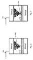
- FIG. 2is a simplified diagram of a resistive switching device 200 according to an embodiment of the present invention.
- the resistance switching deviceis formed overlying a substrate in a specific embodiment.
- the substratecan be a semiconductor substrate having one or more CMOS devices formed thereon.
- the one or more CMOS devicesare operably coupled to the resistive switching device providing controlling circuitry for the memory device in a specific embodiment.
- the resistive switching deviceincludes a first metal electrode 202 , a second metal electrode 204 , a switching layer 206 , and a buffer layer 208 .
- the buffer layeris disposed between the switching layer and the first electrode in a specific embodiment.
- the first metal electrodecan be formed from metal material such as copper, aluminum, or tungsten depending on the application.
- the first metal electrodecan further include one or more adhesion layer or barrier layer to prevent metal from the first electrode to diffusion into other parts of the device or an adhesion layer to prevent the metal material to delaminate from, for example, the dielectric layer, depending on the embodiment.
- the resistive switching deviceincludes switching layer 206 .
- the switching layercomprises an amorphous silicon material.
- the amorphous silicon materialis undoped or having a semiconductor characteristic in a specific embodiment.
- the amorphous silicon materialincludes a plurality of defect sites. The plurality of defect sites can arise from silicon dangling bonds, or atomic dislocations, or crystal plane dislocation, or molecular dislocation, or grain boundaries between silicon crystals depending on the process condition.
- Resistive switching device 200includes second metal electrode 204 overlying the switching layer.
- the second metal electrodeincludes a metal material, which has a high diffusivity in the switching material in a specific embodiment.
- the metal materialcan be silver, copper, aluminum, or other suitable metal materials, including alloy or a combination.
- the metal materialcan be silver for an amorphous silicon material as the switching layer.
- the silver materialforms just a portion of a wiring structure for the switching device, while other portions of the wiring structure comprises convention conducting material such as tungsten, copper or aluminum in a specific embodiment.
- the silver materialis in contact with the amorphous silicon material.
- the defect density at the interface region formed from the first metal electrode and the amorphous silicon material in a conventional structureis high.
- the silver particles in the filament structureare close to each other resulting in a high on state current. After certain number of on/off cycles, the silver particles may coalesce and the silver particles may not be able to retract in an off cycle forming a short between the second electrode and the first electrode, and the device becomes defective.
- buffer layer 208is disposed between the first metal electrode and the switching layer. The buffer layer is provided to prevent an interface region to form from the amorphous silicon material and the first electrode and to control defect density of amorphous silicon and metal particles near the first electrode.
- the buffer layeris selected to have a good and reliable adhesion with the first electrode as well as the amorphous silicon layer. Additionally, an interface region formed from the amorphous silicon material and the buffer layer should have a small defect density for reliable switching and good endurance.
- the buffer layeris engineered, for example, by adjusting buffer layer resistance, to provide a suitable on state resistance and power consumption during programming.
- a first positive voltage 304when a first positive voltage 304 is applied to the second electrode of an as fabricated device, a local electric field is generated and silver particles in various forms, including atoms, ions, or clusters are formed in the amorphous silicon material in a specific embodiment. More specifically, silver particles are formed and trapped in defect sites of the amorphous silicon material. The local electric field enhances silver diffusion in the amorphous silicon material and forms a metal region 302 comprises of the silver particles in a specific embodiment.
- This first positive voltagecan be in the range of 4 volts to about 6 volts depending on the process condition of the amorphous silicon material. As shown the metal region is formed in vicinity of the second electrode surface region, and not in contact with the first electrode.
- the first positive voltageis a forming voltage or electroforming voltage for the switching device. The switching device is in now in an off state.
- a filament structure 402 extending from the metal regionis formed.
- the buffer layerfunctions as a blocking layer such that the filament structure would not extend to be in contact with the first electrode in a specific embodiment.
- the second voltagecan be, for example, a write voltage for the switching device in a specific embodiment.
- the switching deviceis in an on state and an on state current flow s between the second electrode and the first electrode.
- the on state currentis controlled by the length of the filament structure in a specific embodiment. In a specific embodiment, the on state current can range from a few nano amperes to micro amperes, much less than that of a conventional switching device absent of the buffer layer.
- the buffer layershould have good contact with the first electrode to allow a low contact resistance (or forming an ohmic contact) in a contact region formed from the buffer layer and the first electrode.
- the low contact resistanceavoids excess voltage drop across the contact region in a specific embodiment.
- FIG. 5( a )illustrates a switching characteristic of a first switching device having a non-ohmic contact (that is, high contact resistance) between the buffer layer and the first electrode.
- the high contact resistance between the buffer layer and the first electrodesuppresses current flow at small bias and certain read operation at low voltage cannot be performed properly.
- the first switching deviceis further characterized by a high programming voltage (>5 volts) and may cause an early device failure and high leakage current, among others.
- FIG. 5( b )illustrates a switching characteristic of a second switching device having a good ohmic contact between the buffer layer and the first electrode or the contact resistance is low.
- the second switching deviceexhibits desirable switching characteristic, for example, low programming voltage, between 1-2 volts.
- the buffer layercan include an insulating layer.
- the insulating layershould be thin, for example less than about 2 nm, so that electrons can tunnel across the thin insulating buffer layer from a conducting metal region, for example, silver particles in the switching layer and the first electrode. Electron tunneling allows for the device to be in an on state when a suitable voltage is applied to the electrodes. Electron tunneling also allows for proper read operation of the device when a small bias voltage is applied. The contact resistance between such buffer layer and the first electrode may not be as critical in a specific embodiment.
- the buffer layercan include a material having a higher density than the amorphous silicon material to prevent silver particles from being injected into the buffer layer and forming conducting filament in the buffer layer.
- the buffer layercan be conductive having a large thickness (for example, about 20 nm or greater).
- resistive switching devices using amorphous silicon as the switching material and silver as the second electrodecan have vastly different switching characteristics depending on the deposition process of amorphous silicon material.
- amorphous silicon materialis formed using a sputtering process, a high voltage, greater than about 8 volts is required to read, to write or to erase. This suggests that silver particles do not form easily in the sputtered amorphous silicon at normal device operation voltage.
- Sputtered amorphous siliconcontains an insignificant amount of hydrogen and tends to have a high density.
- a thin (preferably less than 5 nm) sputtered amorphous siliconcan be used as the buffer layer in a specific embodiment.
- Amorphous silicon formed using a plasma enhanced chemical vapor deposition (PECVD) or a low pressure chemical vapor deposition (LPCVD) process and silane as a silicon sourceswitching voltages are usually lower, ranging from one to four volts, depending on the process conditions.
- Amorphous silicon material formed by a CVD process using silanecontains hydrogen, which can diffuse or migrate in and out of the silicon matrix, leaving void sites in the material. Silver particles can occupy these void sites or defect sites and allow to migrate upon application of a voltage. It has also been observed that devices merely uses a metal/amorphous silicon/metal configuration have a low on/off endurance, that is such device fails after at most a few thousand on/off cycles.
- the buffer layercan include a polysilicon material.
- the polysilicon materialis preferably p+ doped and having an impurity concentration ranging from about 10 18 to about 10 22 atoms per cm 3 .
- a current versus voltage (I-V) plot 600 of a third switching deviceis provided.
- the third switching devicehas a silver/amorphous silicon/p+ polysilicon device structure.
- the amorphous silicon material in the third switching deviceis deposited using a low pressure chemical vapor deposition process at a deposition temperature of about 510 Degree Celsius using silane as a silicon source.
- FIG. 7illustrates an I-V plot 700 measured from a fourth switching device having a conventional silver/amorphous silicon/nickel device structure.
- the amorphous silicon in the second switching deviceis deposited using a plasma enhanced chemical vapor deposition process at a deposition temperature of about 370 Degree Celsius.
- Both the third switching device and the fourth switching devicehave a cell size of about 60 nm by 60 nm.
- amorphous silicon material deposited at 370 Degree Celsius by a CVD methodhas a much lower defect density than one deposited at 510 Degree Celsius.
- the fourth deviceis thus expected to have a lower on state current than that of the third switching device.
- the on state current of the fourth device(plot 700 ) is much higher, in mA range, than that of the third device (plot 600 ). High current is not desirable as it results in an unreliable device operation.
- the polysilicon buffer layer in the third switching deviceprevents excess defect density near the first electrode, and the programming current is much lower, in the uA range, as shown in plot 600 . Additionally, the polysilicon buffer layer can be modified easily, by changing its thickness or conductivity to control the programming current and further enhance device performance.
- One skilled in the artwould recognize other variations, modifications, and alternatives.
- a method of forming a resistive switching deviceincludes providing a semiconductor substrate having a surface region.
- the semiconductor substratecan have one or more CMOS devices formed thereon.
- the semiconductor substratecan be single crystal silicon material, silicon germanium, silicon on insulator, and the likes.
- a first dielectric materialis formed overlying the surface region.
- the first dielectric materialcan be silicon oxide, silicon nitride, silicon oxynitride, and others.
- the first dielectric materialcan be deposited using techniques such as chemical vapor deposition including plasma enhanced chemical vapor deposition, physical vapor deposition, spin on coating, and any combinations of these, and others.
- the methodincludes forming a first electrode overlying the first dielectric material.
- the first electrodeis formed from a conductor material commonly used in semiconductor processing.
- the conductor materialcan include tungsten, copper, or aluminum depending on the application.
- the first electrodecan include one or more adhesion layer or diffusion barrier.
- the adhesion layermay be titanium, titanium nitride, tantalum nitride, or tungsten nitride to prevent diffusion of the conductor material into the first dielectric material in a specific embodiment.
- the conductor materialcan be deposited using a physical vapor deposition process, a chemical vapor deposition process, electrochemical including electroplating and electroless plating, and combination thereof.
- the conductor material including the adhesion layeris subjected to a pattern and etch process to form a first electrode.
- the first structureis configured to extend in a first direction.
- the methodincludes depositing a buffer layer overlying the first electrode in a specific embodiment.
- the buffer layershould have properties to allow desirable switching characteristic for the switching device.
- the buffer layershould also form a reliable interface with selected switching material used in the switching device.
- a high density materialmay be used to prevent metal particles to inject into the buffer layer.
- the buffer layercan be a conductive material or an insulating material depending on the embodiment.
- a conductive buffer layercan include a p-doped silicon material such as p+ polysilicon material in a specific embodiment.
- An insulating buffer layershould have a thickness less than about 5 nm so that electrons can tunnel through at operating voltages (between 1-3 volts).
- a polysilicon materialcan be used for the buffer layer.
- the polysilicon materialis preferably having a p+ type impurity characteristic, which may be provided using a boron species in a specific embodiment.
- the p+ polysilicon materialmay be deposited using a chemical vapor deposition technique using at least silane, disilane, or a suitable chlorosilane as precursor.
- the methodforms a switching material overlying the buffer material.
- the switching materialis an amorphous silicon material deposited using techniques such as chemical vapor deposition using silane, disilane, or chlorosilane as silicon source. Deposition temperatures is usually at about 250 Degree Celsius to about 600 Degree Celsius depending on the embodiment. Process parameters and process conditions greatly influence defect density in the amorphous silicon material and switching behavior of the switching device. Therefore, the use of amorphous silicon switching material provides flexibility in device design in a specific embodiment.
- the methodincludes depositing a second electrode material overlying the switching material.
- the second electrode materialhas a first portion that includes a metal material in direct contact with the switching material.
- the metal materialis preferably having a suitable diffusion characteristic in the amorphous silicon material in a preferred embodiment.
- the metal materialcan be silver in a specific embodiment. Other suitable metal materials may also be used. These other materials can include platinum, palladium, gold, copper, nickel, and others.
- the second electrode materialfurther includes a second portion for electrical connection with other devices. The second portion can be selected from tungsten, copper, or aluminum, commonly used in semiconductor processing.
- the methodforms a second electrode structure by a suitable pattern and etch process.
- the second electrode structureis configured to extend in a second direction at an angle to the first direction.
- the second electrode structure and the first electrode structureare arranged orthogonal to each other having a switching element sandwiched at an intersecting region formed from the second electrode and the first electrode.
- the methodthen performs other backend processes such as global interconnects and passivation among others to form a resistive switching memory device.
Landscapes
- Engineering & Computer Science (AREA)
- Manufacturing & Machinery (AREA)
- Computer Networks & Wireless Communication (AREA)
- Signal Processing (AREA)
- Semiconductor Memories (AREA)
- Semiconductor Integrated Circuits (AREA)
- Design And Manufacture Of Integrated Circuits (AREA)
Abstract
Description
N/A
The present invention is related to switching devices. More particularly, the present invention provides a structure for a resistive switching memory device. The resistive switching memory device has a reduced on state current to provide improved switching and endurance properties, among others.
The success of semiconductor devices has been mainly driven by an intensive transistor down-scaling process. However, as field effect transistors (FET) approach sizes less than 100 nm, problems such as short channel effect start to prevent proper device operation. Moreover,such sub 100 nm device size can lead to sub-threshold slope non-scaling and also increases power dissipation. It is generally believed that transistor based memories such as those commonly known as Flash may approach an end to scaling within a decade. Flash memory is one type of non-volatile memory device.
Other non-volatile random access memory (RAM) devices such as ferroelectric RAM (Fe RAM), magneto-resistive RAM (MRAM), organic RAM (ORAM), and phase change RAM (PCRAM), among others, have been explored as next generation memory devices. These devices often require new materials and device structures to couple with silicon based devices to form a memory cell, which lack one or more key attributes. For example, Fe-RAM and MRAM devices have fast switching characteristics and good programming endurance, but their fabrication is not CMOS compatible and size is usually large. Switching for a PCRAM device uses Joules heating, which inherently has high power consumption. Organic RAM or ORAM is incompatible with large volume silicon based fabrication and device reliability is usually poor.
From the above, an improved semiconductor memory device and techniques are therefore desirable.
The present invention is related to switching devices. More particularly, the present invention provides a structure for a resistive switching memory device. The resistive switching memory device has a reduced on state current for improved switching and endurance properties, among others.
In a specific embodiment, a switching device structure is provided. The switching device includes a substrate having a surface region and a first dielectric material overlying the surface region. A first electrode overlies the first dielectric material. In a specific embodiment, the first electrode includes at least a metal material. The switching device includes a switching element and a buffer material disposed between the first electrode and the switching element. In a specific embodiment, the buffer material provides a blocking region between the switching material and the first electrode. The switching device includes a second electrode overlying the switching material. The second electrode includes at least a second metal material in a specific embodiment. In a specific embodiment, the blocking region is substantially free of metal particles formed from the second metal material when a first voltage (for example, a write voltage) is applied to the second electrode. In a specific embodiment, the buffer material prevents a high defect region to form between the switching material and the first electrode.
Many benefits are achieved by ways of present invention over conventional techniques. For example, the present resistive switching device can be fabricated using conventional equipment and processes. In addition, the present device uses a layer structure to reduce an on state current as well as power consumption. The layer structure further prevents an electrical connection between the electrodes and improves device endurance and reliability. Depending on the embodiment, one or more of these benefits may be realized. One skilled in the art would recognize other variations, modifications and alternatives.
The present invention is related to switching devices. More particularly, the present invention provides a structure for a resistive switching memory device. The resistive switching memory device is characterized by a reduced on state current for improved switching and endurance properties, among others.
Resistive switching memory device using a non-crystalline silicon such as amorphous silicon, amorphous-polysilicon and microcrystalline silicon as a switching material and metal electrodes has shown promises in a new class of high density memory devices for fast switching. As merely for illustration, amorphous silicon is used to describe non-crystalline silicon. The on/off behavior of the device depends on metal particles formed in defect sites within the amorphous silicon material. Due to mismatch of materials, defect level in an interface region formed from the amorphous silicon material and a metal electrode is high. As metal particles are formed in the defect sites of amorphous silicon material, these devices usually have a high on state current. Upon repeated cycling, the high on state current leads to shorting of the electrodes and device reliability and endurance are compromised, usually less than a few thousand on/off cycles. Embodiments according to the present invention provide a method and a structure to optimize on state current and improve endurance to more than 106on/off cycles, well suitable to be used in current and next generation memory devices.
The terms “second” or “first” throughout the present application are for description and illustration only and should not be construed as the physical arrangement of the electrodes.FIG. 2 is a simplified diagram of aresistive switching device 200 according to an embodiment of the present invention. The resistance switching device is formed overlying a substrate in a specific embodiment. The substrate can be a semiconductor substrate having one or more CMOS devices formed thereon. The one or more CMOS devices are operably coupled to the resistive switching device providing controlling circuitry for the memory device in a specific embodiment. As shown, the resistive switching device includes afirst metal electrode 202, asecond metal electrode 204, aswitching layer 206, and abuffer layer 208. As shown, the buffer layer is disposed between the switching layer and the first electrode in a specific embodiment.
In a specific embodiment, the first metal electrode can be formed from metal material such as copper, aluminum, or tungsten depending on the application. In a specific embodiment, the first metal electrode can further include one or more adhesion layer or barrier layer to prevent metal from the first electrode to diffusion into other parts of the device or an adhesion layer to prevent the metal material to delaminate from, for example, the dielectric layer, depending on the embodiment.
Referring toFIG. 2 , the resistive switching device includes switchinglayer 206. In a specific embodiment, the switching layer comprises an amorphous silicon material. The amorphous silicon material is undoped or having a semiconductor characteristic in a specific embodiment. In a specific embodiment, the amorphous silicon material includes a plurality of defect sites. The plurality of defect sites can arise from silicon dangling bonds, or atomic dislocations, or crystal plane dislocation, or molecular dislocation, or grain boundaries between silicon crystals depending on the process condition.
As described, due to material mismatch between the amorphous silicon material and the first electrode, the defect density at the interface region formed from the first metal electrode and the amorphous silicon material in a conventional structure is high. The silver particles in the filament structure are close to each other resulting in a high on state current. After certain number of on/off cycles, the silver particles may coalesce and the silver particles may not be able to retract in an off cycle forming a short between the second electrode and the first electrode, and the device becomes defective. In a specific embodiment,buffer layer 208 is disposed between the first metal electrode and the switching layer. The buffer layer is provided to prevent an interface region to form from the amorphous silicon material and the first electrode and to control defect density of amorphous silicon and metal particles near the first electrode. The buffer layer is selected to have a good and reliable adhesion with the first electrode as well as the amorphous silicon layer. Additionally, an interface region formed from the amorphous silicon material and the buffer layer should have a small defect density for reliable switching and good endurance. The buffer layer is engineered, for example, by adjusting buffer layer resistance, to provide a suitable on state resistance and power consumption during programming.
Referring toFIG. 3 , when a firstpositive voltage 304 is applied to the second electrode of an as fabricated device, a local electric field is generated and silver particles in various forms, including atoms, ions, or clusters are formed in the amorphous silicon material in a specific embodiment. More specifically, silver particles are formed and trapped in defect sites of the amorphous silicon material. The local electric field enhances silver diffusion in the amorphous silicon material and forms ametal region 302 comprises of the silver particles in a specific embodiment. This first positive voltage can be in the range of 4 volts to about 6 volts depending on the process condition of the amorphous silicon material. As shown the metal region is formed in vicinity of the second electrode surface region, and not in contact with the first electrode. In a specific embodiment, the first positive voltage is a forming voltage or electroforming voltage for the switching device. The switching device is in now in an off state.
Referring toFIG. 4 , when asecond voltage 404 is applied to the second electrode, afilament structure 402 extending from the metal region is formed. As shown, the buffer layer functions as a blocking layer such that the filament structure would not extend to be in contact with the first electrode in a specific embodiment. The second voltage can be, for example, a write voltage for the switching device in a specific embodiment. The switching device is in an on state and an on state current flow s between the second electrode and the first electrode. The on state current is controlled by the length of the filament structure in a specific embodiment. In a specific embodiment, the on state current can range from a few nano amperes to micro amperes, much less than that of a conventional switching device absent of the buffer layer.
In a specific embodiment, for a proper function of a resistive switching device, the buffer layer should have good contact with the first electrode to allow a low contact resistance (or forming an ohmic contact) in a contact region formed from the buffer layer and the first electrode. The low contact resistance avoids excess voltage drop across the contact region in a specific embodiment.FIG. 5( a) illustrates a switching characteristic of a first switching device having a non-ohmic contact (that is, high contact resistance) between the buffer layer and the first electrode. The high contact resistance between the buffer layer and the first electrode suppresses current flow at small bias and certain read operation at low voltage cannot be performed properly. The first switching device is further characterized by a high programming voltage (>5 volts) and may cause an early device failure and high leakage current, among others.FIG. 5( b) illustrates a switching characteristic of a second switching device having a good ohmic contact between the buffer layer and the first electrode or the contact resistance is low. The second switching device exhibits desirable switching characteristic, for example, low programming voltage, between 1-2 volts.
In certain embodiments, the buffer layer can include an insulating layer. The insulating layer should be thin, for example less than about 2 nm, so that electrons can tunnel across the thin insulating buffer layer from a conducting metal region, for example, silver particles in the switching layer and the first electrode. Electron tunneling allows for the device to be in an on state when a suitable voltage is applied to the electrodes. Electron tunneling also allows for proper read operation of the device when a small bias voltage is applied. The contact resistance between such buffer layer and the first electrode may not be as critical in a specific embodiment.
In a specific embodiment, the buffer layer can include a material having a higher density than the amorphous silicon material to prevent silver particles from being injected into the buffer layer and forming conducting filament in the buffer layer. In an alternative embodiment, the buffer layer can be conductive having a large thickness (for example, about 20 nm or greater). Of course one skilled in the art would recognize other variations, modifications, and alternatives.
It has been observed that resistive switching devices using amorphous silicon as the switching material and silver as the second electrode can have vastly different switching characteristics depending on the deposition process of amorphous silicon material. When the amorphous silicon material is formed using a sputtering process, a high voltage, greater than about 8 volts is required to read, to write or to erase. This suggests that silver particles do not form easily in the sputtered amorphous silicon at normal device operation voltage. Sputtered amorphous silicon contains an insignificant amount of hydrogen and tends to have a high density. Hence a thin (preferably less than 5 nm) sputtered amorphous silicon can be used as the buffer layer in a specific embodiment.
For amorphous silicon formed using a plasma enhanced chemical vapor deposition (PECVD) or a low pressure chemical vapor deposition (LPCVD) process and silane as a silicon source, switching voltages are usually lower, ranging from one to four volts, depending on the process conditions. Amorphous silicon material formed by a CVD process using silane contains hydrogen, which can diffuse or migrate in and out of the silicon matrix, leaving void sites in the material. Silver particles can occupy these void sites or defect sites and allow to migrate upon application of a voltage. It has also been observed that devices merely uses a metal/amorphous silicon/metal configuration have a low on/off endurance, that is such device fails after at most a few thousand on/off cycles.
As merely an example, the buffer layer can include a polysilicon material. The polysilicon material is preferably p+ doped and having an impurity concentration ranging from about 1018to about 1022atoms per cm3. As shown inFIG. 6 , a current versus voltage (I-V)plot 600 of a third switching device is provided. The third switching device has a silver/amorphous silicon/p+ polysilicon device structure. The amorphous silicon material in the third switching device is deposited using a low pressure chemical vapor deposition process at a deposition temperature of about 510 Degree Celsius using silane as a silicon source.
In a specific embodiment, a method of forming a resistive switching device is provided. The method includes providing a semiconductor substrate having a surface region. The semiconductor substrate can have one or more CMOS devices formed thereon. The semiconductor substrate can be single crystal silicon material, silicon germanium, silicon on insulator, and the likes. A first dielectric material is formed overlying the surface region. The first dielectric material can be silicon oxide, silicon nitride, silicon oxynitride, and others. The first dielectric material can be deposited using techniques such as chemical vapor deposition including plasma enhanced chemical vapor deposition, physical vapor deposition, spin on coating, and any combinations of these, and others.
In a specific embodiment, the method includes forming a first electrode overlying the first dielectric material. The first electrode is formed from a conductor material commonly used in semiconductor processing. The conductor material can include tungsten, copper, or aluminum depending on the application. The first electrode can include one or more adhesion layer or diffusion barrier. The adhesion layer may be titanium, titanium nitride, tantalum nitride, or tungsten nitride to prevent diffusion of the conductor material into the first dielectric material in a specific embodiment. Depending on the application, the conductor material can be deposited using a physical vapor deposition process, a chemical vapor deposition process, electrochemical including electroplating and electroless plating, and combination thereof. The conductor material including the adhesion layer is subjected to a pattern and etch process to form a first electrode. In a specific embodiment, the first structure is configured to extend in a first direction. Of course one skilled in the art would recognize other variations, modifications, and alternatives.
The method includes depositing a buffer layer overlying the first electrode in a specific embodiment. The buffer layer should have properties to allow desirable switching characteristic for the switching device. The buffer layer should also form a reliable interface with selected switching material used in the switching device. A high density material may be used to prevent metal particles to inject into the buffer layer. The buffer layer can be a conductive material or an insulating material depending on the embodiment. A conductive buffer layer can include a p-doped silicon material such as p+ polysilicon material in a specific embodiment. An insulating buffer layer should have a thickness less than about 5 nm so that electrons can tunnel through at operating voltages (between 1-3 volts).
For an amorphous silicon material as switching material, a polysilicon material can be used for the buffer layer. The polysilicon material is preferably having a p+ type impurity characteristic, which may be provided using a boron species in a specific embodiment. The p+ polysilicon material may be deposited using a chemical vapor deposition technique using at least silane, disilane, or a suitable chlorosilane as precursor.
The method forms a switching material overlying the buffer material. As merely an example, the switching material is an amorphous silicon material deposited using techniques such as chemical vapor deposition using silane, disilane, or chlorosilane as silicon source. Deposition temperatures is usually at about 250 Degree Celsius to about 600 Degree Celsius depending on the embodiment. Process parameters and process conditions greatly influence defect density in the amorphous silicon material and switching behavior of the switching device. Therefore, the use of amorphous silicon switching material provides flexibility in device design in a specific embodiment.
In a specific embodiment, the method includes depositing a second electrode material overlying the switching material. The second electrode material has a first portion that includes a metal material in direct contact with the switching material. The metal material is preferably having a suitable diffusion characteristic in the amorphous silicon material in a preferred embodiment. The metal material can be silver in a specific embodiment. Other suitable metal materials may also be used. These other materials can include platinum, palladium, gold, copper, nickel, and others. The second electrode material further includes a second portion for electrical connection with other devices. The second portion can be selected from tungsten, copper, or aluminum, commonly used in semiconductor processing. The method forms a second electrode structure by a suitable pattern and etch process. In a specific embodiment, the second electrode structure is configured to extend in a second direction at an angle to the first direction. In a preferred embodiment the second electrode structure and the first electrode structure are arranged orthogonal to each other having a switching element sandwiched at an intersecting region formed from the second electrode and the first electrode. One skilled in the art would recognized other variations, modifications, and alternatives.
The method then performs other backend processes such as global interconnects and passivation among others to form a resistive switching memory device.
Though the present invention has been described using various examples and embodiments, it is also understood that the examples and embodiments described herein are for illustrative purposes only and that various modifications or alternatives in light thereof will be suggested to persons skilled in the art and are to be included within the spirit and purview of this application and scope of the appended claims.
Claims (22)
1. A resistive switching device, comprising:
a first electrode comprising a first metal material;
a second electrode comprising at least a second metal material;
a switching material, the switching material comprising a non-conductive material having non-stoichiometric sites, wherein the non-stoichiometric sites are configured to trap metal particles of the second metal material derived from the second electrode therein;
and
a buffer material disposed between the first electrode and the switching material and completely separating the first electrode and the switching material, the buffer material providing a blocking region between the switching material and the first electrode, the blocking region being substantially free from the metal particles from the second metal material when a first voltage is applied to the second electrode.
2. The device ofclaim 1 wherein the first voltage is a write voltage or a read voltage.
3. The device ofclaim 1 wherein the second metal material is selected from a group consisting of: Silver, Copper, Aluminum, metal alloy.
4. The device ofclaim 1 wherein the second metal material is selected from a group consisting of: a silver material, a platinum material, or a palladium material.
5. The device ofclaim 1 wherein the buffer material has a thickness of less than about 2 nm.
6. The device ofclaim 1 wherein the first voltage causes a first on state current upon application of the first voltage, the first voltage being a write voltage.
7. The device ofclaim 1 wherein the buffer material comprises amorphous silicon.
8. The device ofclaim 1 wherein the buffer material comprises a polycrystalline silicon-containing material having a p+ impurity characteristic.
9. The device ofclaim 1 wherein the buffer material is characterized by a thickness to allow for tunneling of electrons across the buffer material upon application of the first voltage.
10. The device ofclaim 1 wherein the buffer material is a conductive material.
11. The device ofclaim 1 wherein the buffer material is characterized by a density, the density prevents the metal particles to form metal regions or conducting filaments in the buffer material.
12. The device ofclaim 1 wherein the blocking region prevents the accumulation of metal particles in a vicinity of the first electrode.
13. The device ofclaim 1 wherein the buffer material comprises a silicon material substantially free from hydrogen species.
14. The device ofclaim 4 wherein the second metal material forms a metal region comprising the metal particles in a portion of the switching material in a vicinity of the second electrode upon applying a positive voltage larger than a first threshold voltage to the second electrode.
15. The device ofclaim 4 wherein the buffer material inhibits the metal particles from contacting the first electrode.
16. The device ofclaim 6 wherein the first on state current is less than a second on state current, the second on state current being caused by a second device absent of the buffer material upon application of the first voltage.
17. The device ofclaim 8 wherein the p+ impurity characteristic is provided by a boron species at a concentration within a range of about 1E18 atoms per cm3to about 1 E22 atoms per cm3.
18. The device ofclaim 9 wherein the first voltage is within a range of about 1 volts to about 3 volts.
19. The device ofclaim 13 wherein the silicon material substantially free from hydrogen species is formed by sputtering or evaporation of silicon.
20. The device ofclaim 14 wherein the first threshold voltage ranges from about 1 volts to about 2 volts.
21. The device ofclaim 14 wherein the metal region further comprises a filament structure characterized by a length, the length being dependent on first applied to the second electrode.
22. The device ofclaim 21 wherein the length of the filament structure is reduced when a reverse bias voltage having an opposite polarity to the first voltage is applied.
Priority Applications (9)
| Application Number | Priority Date | Filing Date | Title |
|---|---|---|---|
| US12/861,432US8884261B2 (en) | 2010-08-23 | 2010-08-23 | Device switching using layered device structure |
| DE112011102804TDE112011102804T5 (en) | 2010-08-23 | 2011-07-29 | Improved switching device with layered device structure |
| CN201180050941.0ACN103180951B (en) | 2010-08-23 | 2011-07-29 | Improved switching devices using layered device/device structures |
| PCT/US2011/046035WO2012027068A2 (en) | 2010-08-23 | 2011-07-29 | Improved device switching using layered device structure |
| KR1020137007430AKR101963150B1 (en) | 2010-08-23 | 2011-07-29 | Improved device switching using layered device structure |
| JP2013525926AJP5808811B2 (en) | 2010-08-23 | 2011-07-29 | Improved device switching utilizing layer structure |
| US14/509,967US9590013B2 (en) | 2010-08-23 | 2014-10-08 | Device switching using layered device structure |
| US14/611,022US9601692B1 (en) | 2010-07-13 | 2015-01-30 | Hetero-switching layer in a RRAM device and method |
| US15/451,045US10224370B2 (en) | 2010-08-23 | 2017-03-06 | Device switching using layered device structure |
Applications Claiming Priority (1)
| Application Number | Priority Date | Filing Date | Title |
|---|---|---|---|
| US12/861,432US8884261B2 (en) | 2010-08-23 | 2010-08-23 | Device switching using layered device structure |
Related Child Applications (1)
| Application Number | Title | Priority Date | Filing Date |
|---|---|---|---|
| US14/509,967ContinuationUS9590013B2 (en) | 2010-07-13 | 2014-10-08 | Device switching using layered device structure |
Publications (2)
| Publication Number | Publication Date |
|---|---|
| US20120043519A1 US20120043519A1 (en) | 2012-02-23 |
| US8884261B2true US8884261B2 (en) | 2014-11-11 |
Family
ID=45593335
Family Applications (3)
| Application Number | Title | Priority Date | Filing Date |
|---|---|---|---|
| US12/861,432Active2032-09-15US8884261B2 (en) | 2010-07-13 | 2010-08-23 | Device switching using layered device structure |
| US14/509,967Expired - Fee RelatedUS9590013B2 (en) | 2010-07-13 | 2014-10-08 | Device switching using layered device structure |
| US15/451,045ActiveUS10224370B2 (en) | 2010-08-23 | 2017-03-06 | Device switching using layered device structure |
Family Applications After (2)
| Application Number | Title | Priority Date | Filing Date |
|---|---|---|---|
| US14/509,967Expired - Fee RelatedUS9590013B2 (en) | 2010-07-13 | 2014-10-08 | Device switching using layered device structure |
| US15/451,045ActiveUS10224370B2 (en) | 2010-08-23 | 2017-03-06 | Device switching using layered device structure |
Country Status (6)
| Country | Link |
|---|---|
| US (3) | US8884261B2 (en) |
| JP (1) | JP5808811B2 (en) |
| KR (1) | KR101963150B1 (en) |
| CN (1) | CN103180951B (en) |
| DE (1) | DE112011102804T5 (en) |
| WO (1) | WO2012027068A2 (en) |
Cited By (5)
| Publication number | Priority date | Publication date | Assignee | Title |
|---|---|---|---|---|
| US20160343937A1 (en)* | 2015-05-22 | 2016-11-24 | Crossbar, Inc. | Non-stoichiometric resistive switching memory device and fabrication methods |
| US10062845B1 (en)* | 2016-05-13 | 2018-08-28 | Crossbar, Inc. | Flatness of memory cell surfaces |
| US10522754B2 (en) | 2016-06-15 | 2019-12-31 | Crossbar, Inc. | Liner layer for dielectric block layer |
| US10608180B2 (en) | 2015-02-03 | 2020-03-31 | Crossbar, Inc. | Resistive memory cell with intrinsic current control |
| US10749110B1 (en) | 2016-07-15 | 2020-08-18 | Crossbar, Inc. | Memory stack liner comprising dielectric block layer material |
Families Citing this family (73)
| Publication number | Priority date | Publication date | Assignee | Title |
|---|---|---|---|---|
| JP5543819B2 (en)* | 2010-03-26 | 2014-07-09 | 株式会社東芝 | Resistance change element, memory cell array, and resistance change device |
| US9570678B1 (en) | 2010-06-08 | 2017-02-14 | Crossbar, Inc. | Resistive RAM with preferental filament formation region and methods |
| US9601692B1 (en) | 2010-07-13 | 2017-03-21 | Crossbar, Inc. | Hetero-switching layer in a RRAM device and method |
| US8946046B1 (en) | 2012-05-02 | 2015-02-03 | Crossbar, Inc. | Guided path for forming a conductive filament in RRAM |
| US9012307B2 (en) | 2010-07-13 | 2015-04-21 | Crossbar, Inc. | Two terminal resistive switching device structure and method of fabricating |
| CN103081093B (en) | 2010-06-11 | 2015-06-03 | 科洛斯巴股份有限公司 | Pillar structure and method of memory device |
| US8441835B2 (en) | 2010-06-11 | 2013-05-14 | Crossbar, Inc. | Interface control for improved switching in RRAM |
| US8374018B2 (en) | 2010-07-09 | 2013-02-12 | Crossbar, Inc. | Resistive memory using SiGe material |
| US8467227B1 (en) | 2010-11-04 | 2013-06-18 | Crossbar, Inc. | Hetero resistive switching material layer in RRAM device and method |
| US8947908B2 (en) | 2010-11-04 | 2015-02-03 | Crossbar, Inc. | Hetero-switching layer in a RRAM device and method |
| US8884261B2 (en) | 2010-08-23 | 2014-11-11 | Crossbar, Inc. | Device switching using layered device structure |
| US8168506B2 (en) | 2010-07-13 | 2012-05-01 | Crossbar, Inc. | On/off ratio for non-volatile memory device and method |
| US8569172B1 (en) | 2012-08-14 | 2013-10-29 | Crossbar, Inc. | Noble metal/non-noble metal electrode for RRAM applications |
| US8889521B1 (en) | 2012-09-14 | 2014-11-18 | Crossbar, Inc. | Method for silver deposition for a non-volatile memory device |
| US9401475B1 (en) | 2010-08-23 | 2016-07-26 | Crossbar, Inc. | Method for silver deposition for a non-volatile memory device |
| US8404553B2 (en) | 2010-08-23 | 2013-03-26 | Crossbar, Inc. | Disturb-resistant non-volatile memory device and method |
| US8492195B2 (en) | 2010-08-23 | 2013-07-23 | Crossbar, Inc. | Method for forming stackable non-volatile resistive switching memory devices |
| US8558212B2 (en) | 2010-09-29 | 2013-10-15 | Crossbar, Inc. | Conductive path in switching material in a resistive random access memory device and control |
| US8391049B2 (en) | 2010-09-29 | 2013-03-05 | Crossbar, Inc. | Resistor structure for a non-volatile memory device and method |
| USRE46335E1 (en) | 2010-11-04 | 2017-03-07 | Crossbar, Inc. | Switching device having a non-linear element |
| US8502185B2 (en) | 2011-05-31 | 2013-08-06 | Crossbar, Inc. | Switching device having a non-linear element |
| US8088688B1 (en) | 2010-11-05 | 2012-01-03 | Crossbar, Inc. | p+ polysilicon material on aluminum for non-volatile memory device and method |
| US8930174B2 (en) | 2010-12-28 | 2015-01-06 | Crossbar, Inc. | Modeling technique for resistive random access memory (RRAM) cells |
| US8487293B2 (en)* | 2010-12-30 | 2013-07-16 | Micron Technology, Inc. | Bipolar switching memory cell with built-in “on ”state rectifying current-voltage characteristics |
| US9153623B1 (en) | 2010-12-31 | 2015-10-06 | Crossbar, Inc. | Thin film transistor steering element for a non-volatile memory device |
| US8815696B1 (en) | 2010-12-31 | 2014-08-26 | Crossbar, Inc. | Disturb-resistant non-volatile memory device using via-fill and etchback technique |
| US8791010B1 (en) | 2010-12-31 | 2014-07-29 | Crossbar, Inc. | Silver interconnects for stacked non-volatile memory device and method |
| JP5364739B2 (en)* | 2011-02-18 | 2013-12-11 | 株式会社東芝 | Nonvolatile resistance change element |
| US8450710B2 (en) | 2011-05-27 | 2013-05-28 | Crossbar, Inc. | Low temperature p+ silicon junction material for a non-volatile memory device |
| US9620206B2 (en) | 2011-05-31 | 2017-04-11 | Crossbar, Inc. | Memory array architecture with two-terminal memory cells |
| US8619459B1 (en) | 2011-06-23 | 2013-12-31 | Crossbar, Inc. | High operating speed resistive random access memory |
| US9627443B2 (en) | 2011-06-30 | 2017-04-18 | Crossbar, Inc. | Three-dimensional oblique two-terminal memory with enhanced electric field |
| US8946669B1 (en) | 2012-04-05 | 2015-02-03 | Crossbar, Inc. | Resistive memory device and fabrication methods |
| US8659929B2 (en) | 2011-06-30 | 2014-02-25 | Crossbar, Inc. | Amorphous silicon RRAM with non-linear device and operation |
| US9166163B2 (en) | 2011-06-30 | 2015-10-20 | Crossbar, Inc. | Sub-oxide interface layer for two-terminal memory |
| US9564587B1 (en) | 2011-06-30 | 2017-02-07 | Crossbar, Inc. | Three-dimensional two-terminal memory with enhanced electric field and segmented interconnects |
| US9252191B2 (en) | 2011-07-22 | 2016-02-02 | Crossbar, Inc. | Seed layer for a p+ silicon germanium material for a non-volatile memory device and method |
| US10056907B1 (en) | 2011-07-29 | 2018-08-21 | Crossbar, Inc. | Field programmable gate array utilizing two-terminal non-volatile memory |
| US8674724B2 (en) | 2011-07-29 | 2014-03-18 | Crossbar, Inc. | Field programmable gate array utilizing two-terminal non-volatile memory |
| US9729155B2 (en) | 2011-07-29 | 2017-08-08 | Crossbar, Inc. | Field programmable gate array utilizing two-terminal non-volatile memory |
| JP5537524B2 (en)* | 2011-09-22 | 2014-07-02 | 株式会社東芝 | Resistance change memory |
| US8716098B1 (en)* | 2012-03-09 | 2014-05-06 | Crossbar, Inc. | Selective removal method and structure of silver in resistive switching device for a non-volatile memory device |
| US9087576B1 (en) | 2012-03-29 | 2015-07-21 | Crossbar, Inc. | Low temperature fabrication method for a three-dimensional memory device and structure |
| US9685608B2 (en) | 2012-04-13 | 2017-06-20 | Crossbar, Inc. | Reduced diffusion in metal electrode for two-terminal memory |
| US8658476B1 (en)* | 2012-04-20 | 2014-02-25 | Crossbar, Inc. | Low temperature P+ polycrystalline silicon material for non-volatile memory device |
| US8796658B1 (en) | 2012-05-07 | 2014-08-05 | Crossbar, Inc. | Filamentary based non-volatile resistive memory device and method |
| US8765566B2 (en) | 2012-05-10 | 2014-07-01 | Crossbar, Inc. | Line and space architecture for a non-volatile memory device |
| US9583701B1 (en) | 2012-08-14 | 2017-02-28 | Crossbar, Inc. | Methods for fabricating resistive memory device switching material using ion implantation |
| US9741765B1 (en) | 2012-08-14 | 2017-08-22 | Crossbar, Inc. | Monolithically integrated resistive memory using integrated-circuit foundry compatible processes |
| US8946673B1 (en)* | 2012-08-24 | 2015-02-03 | Crossbar, Inc. | Resistive switching device structure with improved data retention for non-volatile memory device and method |
| US9312483B2 (en) | 2012-09-24 | 2016-04-12 | Crossbar, Inc. | Electrode structure for a non-volatile memory device and method |
| US9576616B2 (en) | 2012-10-10 | 2017-02-21 | Crossbar, Inc. | Non-volatile memory with overwrite capability and low write amplification |
| US11068620B2 (en) | 2012-11-09 | 2021-07-20 | Crossbar, Inc. | Secure circuit integrated with memory layer |
| US8982647B2 (en) | 2012-11-14 | 2015-03-17 | Crossbar, Inc. | Resistive random access memory equalization and sensing |
| US9412790B1 (en) | 2012-12-04 | 2016-08-09 | Crossbar, Inc. | Scalable RRAM device architecture for a non-volatile memory device and method |
| US9406379B2 (en) | 2013-01-03 | 2016-08-02 | Crossbar, Inc. | Resistive random access memory with non-linear current-voltage relationship |
| US9112145B1 (en) | 2013-01-31 | 2015-08-18 | Crossbar, Inc. | Rectified switching of two-terminal memory via real time filament formation |
| US9324942B1 (en) | 2013-01-31 | 2016-04-26 | Crossbar, Inc. | Resistive memory cell with solid state diode |
| US8934280B1 (en) | 2013-02-06 | 2015-01-13 | Crossbar, Inc. | Capacitive discharge programming for two-terminal memory cells |
| US9093635B2 (en) | 2013-03-14 | 2015-07-28 | Crossbar, Inc. | Controlling on-state current for two-terminal memory |
| JP2015018591A (en) | 2013-07-12 | 2015-01-29 | 株式会社東芝 | Nonvolatile semiconductor memory device |
| US9793473B2 (en)* | 2013-09-05 | 2017-10-17 | Hewlett Packard Enterprise Development Lp | Memristor structures |
| US9269898B2 (en)* | 2014-02-07 | 2016-02-23 | Crossbar, Inc. | Low temperature deposition for silicon-based conductive film |
| US10290801B2 (en) | 2014-02-07 | 2019-05-14 | Crossbar, Inc. | Scalable silicon based resistive memory device |
| KR102410947B1 (en)* | 2015-11-20 | 2022-06-22 | 에스케이하이닉스 주식회사 | Threshold switching device and electronic device including the same |
| CN105372849B (en)* | 2015-11-27 | 2018-08-24 | 电子科技大学 | A kind of silica-based waveguides photoswitch and its manufacturing method based on non-crystalline silicon memristor effect |
| EP3446463A1 (en)* | 2016-04-22 | 2019-02-27 | Level 3 Communications, LLC | Anycast routing techniques in a network |
| EP3472839A4 (en) | 2016-06-20 | 2020-02-26 | Massachusetts Institute of Technology | DEVICE AND METHOD FOR ELECTRICAL CIRCUIT |
| WO2018057012A1 (en)* | 2016-09-23 | 2018-03-29 | Intel Corporation | Threshold switching selector based memory |
| US10297749B1 (en) | 2017-12-12 | 2019-05-21 | International Business Machines Corporation | High density resistive random access memory integrated on complementary metal oxide semiconductor |
| US20200176379A1 (en)* | 2018-11-30 | 2020-06-04 | Taiwan Semiconductor Manufacturing Co., Ltd. | Metal filament vias for interconnect structure |
| RU2729978C1 (en)* | 2019-11-08 | 2020-08-13 | Федеральное государственное автономное образовательное учреждение высшего образования "Национальный исследовательский Нижегородский государственный университет им. Н.И. Лобачевского" | Method of estimating activation energies of diffusion of oxygen ions in a memristor filament |
| US11552246B2 (en) | 2020-01-21 | 2023-01-10 | Massachusetts Institute Of Technology | Memristors and related systems and methods |
Citations (194)
| Publication number | Priority date | Publication date | Assignee | Title |
|---|---|---|---|---|
| US680652A (en) | 1897-11-08 | 1901-08-13 | Leonard L Elden | Circuit-breaker. |
| US4433468A (en) | 1980-03-26 | 1984-02-28 | Nippon Electric Co., Ltd. | Method for making semiconductor device having improved thermal stress characteristics |
| US4684972A (en) | 1981-08-07 | 1987-08-04 | The British Petroleum Company, P.L.C. | Non-volatile amorphous semiconductor memory device utilizing a forming voltage |
| US4741601A (en) | 1984-10-08 | 1988-05-03 | Nec Corporation | Non-linear device for driving liquid crystal display |
| US5242855A (en) | 1991-09-30 | 1993-09-07 | Nec Corporation | Method of fabricating a polycrystalline silicon film having a reduced resistivity |
| US5278085A (en) | 1992-08-11 | 1994-01-11 | Micron Semiconductor, Inc. | Single mask process for forming both n-type and p-type gates in a polycrystalline silicon layer during the formation of a semiconductor device |
| US5315131A (en) | 1990-11-22 | 1994-05-24 | Matsushita Electric Industrial Co., Ltd. | Electrically reprogrammable nonvolatile memory device |
| US5335219A (en) | 1991-01-18 | 1994-08-02 | Ovshinsky Stanford R | Homogeneous composition of microcrystalline semiconductor material, semiconductor devices and directly overwritable memory elements fabricated therefrom, and arrays fabricated from the memory elements |
| US5360981A (en) | 1989-05-11 | 1994-11-01 | British Telecommunications Public Limited Company | Amorphous silicon memory |
| US5457649A (en) | 1994-08-26 | 1995-10-10 | Microchip Technology, Inc. | Semiconductor memory device and write-once, read-only semiconductor memory array using amorphous-silicon and method therefor |
| US5538564A (en) | 1994-03-18 | 1996-07-23 | Regents Of The University Of California | Three dimensional amorphous silicon/microcrystalline silicon solar cells |
| US5541869A (en) | 1991-10-22 | 1996-07-30 | British Telecommunications, Plc | Resistive memory element |
| US5594363A (en) | 1995-04-07 | 1997-01-14 | Zycad Corporation | Logic cell and routing architecture in a field programmable gate array |
| US5614756A (en) | 1990-04-12 | 1997-03-25 | Actel Corporation | Metal-to-metal antifuse with conductive |
| US5645628A (en) | 1994-07-14 | 1997-07-08 | Matsushita Electric Industrial Co., Ltd. | Electroless plating bath used for forming a wiring of a semiconductor device, and method of forming a wiring of a semiconductor device |
| US5751012A (en) | 1995-06-07 | 1998-05-12 | Micron Technology, Inc. | Polysilicon pillar diode for use in a non-volatile memory cell |
| US5840608A (en) | 1996-11-22 | 1998-11-24 | United Microelectronics Corporation | High density ROM and a method of making the same |
| US5970332A (en) | 1995-03-28 | 1999-10-19 | U.S. Philips Corporation | Method of manufacturing a semiconductor device with a BiCMOS circuit |
| US5998244A (en) | 1996-08-22 | 1999-12-07 | Micron Technology, Inc. | Memory cell incorporating a chalcogenide element and method of making same |
| US6128214A (en) | 1999-03-29 | 2000-10-03 | Hewlett-Packard | Molecular wire crossbar memory |
| US6143642A (en) | 1997-12-22 | 2000-11-07 | Vlsi Technology, Inc. | Programmable semiconductor structures and methods for making the same |
| US6259116B1 (en) | 1997-10-22 | 2001-07-10 | U.S. Philips Corporation | Multiple memory element semiconductor memory devices |
| US6291836B1 (en) | 1996-06-05 | 2001-09-18 | U. S. Philips Corporation | Method of operating a programmable, non-volatile memory device |
| US6436765B1 (en) | 2001-02-09 | 2002-08-20 | United Microelectronics Corp. | Method of fabricating a trenched flash memory cell |
| US6436818B1 (en) | 1997-02-19 | 2002-08-20 | Micron Technology, Inc. | Semiconductor structure having a doped conductive layer |
| US6492694B2 (en) | 1998-02-27 | 2002-12-10 | Micron Technology, Inc. | Highly conductive composite polysilicon gate for CMOS integrated circuits |
| WO2003034498A1 (en) | 2001-10-16 | 2003-04-24 | Midwest Research Institute | Stacked switchable element and diode combination |
| US20030141565A1 (en) | 2002-01-28 | 2003-07-31 | Fumihiko Hirose | Diode |
| US6627530B2 (en) | 2000-12-22 | 2003-09-30 | Matrix Semiconductor, Inc. | Patterning three dimensional structures |
| US20040026682A1 (en) | 2002-06-17 | 2004-02-12 | Hai Jiang | Nano-dot memory and fabricating same |
| US6762474B1 (en) | 1998-06-10 | 2004-07-13 | Agere Systems Inc. | Method and apparatus for temperature compensation of read-only memory |
| US6768157B2 (en) | 2001-08-13 | 2004-07-27 | Advanced Micro Devices, Inc. | Memory device |
| US20040170040A1 (en) | 2002-08-02 | 2004-09-02 | Unity Semiconductor Corporation | Rewritable memory with non-linear memory element |
| US6815286B2 (en) | 2001-08-13 | 2004-11-09 | Advanced Micro Devices, Inc. | Memory device |
| US6838720B2 (en) | 2001-08-13 | 2005-01-04 | Advanced Micro Devices, Inc. | Memory device with active passive layers |
| US20050020510A1 (en) | 2002-08-29 | 2005-01-27 | Benedict Dale L. | D-mannose contraceptives |
| US20050029587A1 (en) | 1995-06-07 | 2005-02-10 | Harshfield Steven T. | Method and apparatus for forming an integrated circuit electrode having a reduced contact area |
| US6858482B2 (en) | 2002-04-10 | 2005-02-22 | Micron Technology, Inc. | Method of manufacture of programmable switching circuits and memory cells employing a glass layer |
| US6858481B2 (en) | 2001-08-13 | 2005-02-22 | Advanced Micro Devices, Inc. | Memory device with active and passive layers |
| US6864127B2 (en) | 1997-04-25 | 2005-03-08 | Semiconductor Energy Laboratory Co., Ltd. | Semiconductor device and method of fabricating the same |
| US20050062045A1 (en) | 2002-10-02 | 2005-03-24 | Arup Bhattacharyya | Processes of forming stacked resistor constructions |
| US6927430B2 (en) | 2001-06-28 | 2005-08-09 | Sharp Laboratories Of America, Inc. | Shared bit line cross-point memory array incorporating P/N junctions |
| US6939787B2 (en) | 1999-12-28 | 2005-09-06 | Fujitsu Limited | Method for fabricating semiconductor device having gate electrode with polymetal structure of polycrystalline silicon film and metal film |
| US6946719B2 (en) | 2003-12-03 | 2005-09-20 | Matrix Semiconductor, Inc | Semiconductor device including junction diode contacting contact-antifuse unit comprising silicide |
| US20060017488A1 (en) | 2004-07-21 | 2006-01-26 | Sharp Laboratories Of America, Inc. | Mono-polarity switchable PCMO resistor trimmer |
| US7020006B2 (en) | 2002-08-02 | 2006-03-28 | Unity Semiconductor Corporation | Discharge of conductive array lines in fast memory |
| US7023093B2 (en) | 2002-10-24 | 2006-04-04 | International Business Machines Corporation | Very low effective dielectric constant interconnect Structures and methods for fabricating the same |
| US7102150B2 (en) | 2001-05-11 | 2006-09-05 | Harshfield Steven T | PCRAM memory cell and method of making same |
| US7122853B1 (en) | 2004-08-17 | 2006-10-17 | Fasl, Inc. | Method to improve yield and simplify operation of polymer memory cells |
| US20060281244A1 (en) | 2005-06-08 | 2006-12-14 | Masayuki Ichige | Nonvolatile semiconductor memory device and method of manufacturing the same |
| US20070008773A1 (en) | 2005-07-11 | 2007-01-11 | Matrix Semiconductor, Inc. | Nonvolatile memory cell comprising switchable resistor and transistor |
| US20070015348A1 (en) | 2005-07-18 | 2007-01-18 | Sharp Laboratories Of America, Inc. | Crosspoint resistor memory device with back-to-back Schottky diodes |
| US20070045615A1 (en) | 2005-08-31 | 2007-03-01 | Samsung Electronics Co., Ltd. | Non-volatile organic resistance random access memory device and method of manufacturing the same |
| US7187577B1 (en) | 2005-11-23 | 2007-03-06 | Grandis, Inc. | Method and system for providing current balanced writing for memory cells and magnetic devices |
| US20070087508A1 (en) | 2003-12-03 | 2007-04-19 | Herner S B | Method for making a p-i-n diode crystallized adjacent to a silicide in series with a dielectric antifuse |
| US20070090425A1 (en) | 2005-09-28 | 2007-04-26 | Matrix Semiconductor, Inc. | Memory cell comprising switchable semiconductor memory element with trimmable resistance |
| US20070105284A1 (en) | 2003-12-03 | 2007-05-10 | Herner S B | Method for forming a memory cell comprising a semiconductor junction diode crystallized adjacent to a silicide |
| US20070105390A1 (en) | 2005-11-09 | 2007-05-10 | Oh Travis B | Oxygen depleted etching process |
| US7221599B1 (en) | 2004-11-01 | 2007-05-22 | Spansion, Llc | Polymer memory cell operation |
| US7238607B2 (en) | 2002-12-19 | 2007-07-03 | Sandisk 3D Llc | Method to minimize formation of recess at surface planarized by chemical mechanical planarization |
| US20070205510A1 (en) | 2006-03-03 | 2007-09-06 | Lavoie Adrien R | Noble metal barrier layers |
| US20070228414A1 (en) | 2006-03-31 | 2007-10-04 | Sandisk 3D, Llc | Heterojunction device comprising a semiconductor and a resistivity-switching oxide or nitride |
| US7289353B2 (en) | 2004-08-17 | 2007-10-30 | Spansion, Llc | Systems and methods for adjusting programming thresholds of polymer memory cells |
| US20070290186A1 (en) | 2006-05-04 | 2007-12-20 | El Mostafa Bourim | Non-volatile variable resistance memory device and method of fabricating the same |
| US20070291527A1 (en) | 2006-06-07 | 2007-12-20 | Sony Corporation | Memory apparatus |
| US20080002481A1 (en) | 2002-12-20 | 2008-01-03 | Dietmar Gogl | Integrated Circuit, Method of Operating an Integrated Circuit, Method of Manufacturing an Integrated Circuit, Memory Module, Stackable Memory Module |
| US20080006907A1 (en) | 2006-07-06 | 2008-01-10 | Samsung Electronics Co., Ltd | Non-volatile memory device including a variable resistance material |
| US7324363B2 (en) | 2005-12-12 | 2008-01-29 | Synopsys, Inc. | SPICE optimized for arrays |
| US20080048164A1 (en) | 2006-07-11 | 2008-02-28 | Matsushita Electric Industrial Co., Ltd. | Electro-resistance element, method of manufacturing the same and electro-resistance memory using the same |
| US20080089110A1 (en) | 2006-10-16 | 2008-04-17 | Warren Robinett | Crossbar-memory systems and methods for writing to and reading from crossbar memory junctions of crossbar-memory systems |
| US20080090337A1 (en) | 2006-10-03 | 2008-04-17 | Williams R Stanley | Electrically actuated switch |
| US7365411B2 (en) | 2004-08-12 | 2008-04-29 | Micron Technology, Inc. | Resistance variable memory with temperature tolerant materials |
| US20080106926A1 (en) | 2006-11-08 | 2008-05-08 | Symetrix Corporation | Non-volatile resistance switching memories and methods of making same |
| US20080106925A1 (en) | 2006-11-08 | 2008-05-08 | Symetrix Corporation | Correlated electron memory |
| US7405418B2 (en) | 2004-02-17 | 2008-07-29 | Infineon Technologies Ag | Memory device electrode with a surface structure |
| US20080185567A1 (en) | 2007-02-05 | 2008-08-07 | Nitin Kumar | Methods for forming resistive switching memory elements |
| US20080206931A1 (en) | 2002-07-26 | 2008-08-28 | Laurent Breuil | Nonvolatile memory element and production method thereof and storage memory arrangement |
| US20080232160A1 (en) | 2007-02-27 | 2008-09-25 | International Business Machines Corporation | Rectifying element for a crosspoint based memory array architecture |
| US20080278990A1 (en) | 2007-05-09 | 2008-11-13 | Pragati Kumar | Resistive-switching nonvolatile memory elements |
| US20080304312A1 (en) | 2007-06-11 | 2008-12-11 | Macronix International Co., Ltd. | Resistance memory with tungsten compound and manufacturing |
| US20080311722A1 (en) | 2007-06-15 | 2008-12-18 | Sandisk 3D Llc | Method for forming polycrystalline thin film bipolar transistors |
| US20090001345A1 (en) | 2007-06-29 | 2009-01-01 | April Schricker | Memory cell that employs a selectively deposited reversible resistance-switching element and methods of forming the same |
| US7474000B2 (en) | 2003-12-05 | 2009-01-06 | Sandisk 3D Llc | High density contact to relaxed geometry layers |
| WO2009005699A1 (en) | 2007-06-29 | 2009-01-08 | Sandisk 3D, Llc | Memory cell that employs a selectively grown reversible resistance-switching element and methods of forming the same |
| US20090014707A1 (en)* | 2006-10-20 | 2009-01-15 | Wei Lu | Non-volatile solid state resistive switching devices |
| US20090052226A1 (en) | 2007-08-24 | 2009-02-26 | Samsung Electronics Co., Ltd | Resistive random access memory device |
| US7499355B2 (en) | 2006-07-31 | 2009-03-03 | Sandisk 3D Llc | High bandwidth one time field-programmable memory |
| US20090095951A1 (en) | 2007-10-12 | 2009-04-16 | Ovonyx, Inc. | Memory Device With Low Reset Current |
| US7521705B2 (en) | 2005-08-15 | 2009-04-21 | Micron Technology, Inc. | Reproducible resistance variable insulating memory devices having a shaped bottom electrode |
| US7534625B2 (en) | 2004-09-24 | 2009-05-19 | Karpov Ilya V | Phase change memory with damascene memory element |
| US7541252B2 (en) | 2006-11-09 | 2009-06-02 | Samsung Electronics Co., Ltd. | Methods of fabricating a semiconductor device including a self-aligned cell diode |
| US20090152737A1 (en) | 2000-07-14 | 2009-06-18 | Micron Technology, Inc. | Memory devices having contact features |
| US7550380B2 (en) | 2004-11-03 | 2009-06-23 | Micron Technology, Inc. | Electroless plating of metal caps for chalcogenide-based memory devices |
| US20090168486A1 (en) | 2007-12-27 | 2009-07-02 | Sandisk 3D Llc | Large capacity one-time programmable memory cell using metal oxides |
| US7566643B2 (en) | 2007-07-23 | 2009-07-28 | Ovonyx, Inc. | Liquid phase deposition of contacts in programmable resistance and switching devices |
| US20090231910A1 (en) | 2008-03-11 | 2009-09-17 | Micron Technology, Inc. | Non-volatile memory with resistive access component |
| US20090250787A1 (en) | 2008-04-07 | 2009-10-08 | Toshie Kutsunai | Semiconductor storage device and manufacturing method of the same |
| US20090257265A1 (en) | 2008-04-11 | 2009-10-15 | Sandisk 3D Llc | Multilevel nonvolatile memory device containing a carbon storage material and methods of making and using same |
| US20090256130A1 (en) | 2008-04-11 | 2009-10-15 | Sandisk 3D Llc | Memory cell that employs a selectively fabricated carbon nano-tube reversible resistance-switching element, and methods of forming the same |
| US7606059B2 (en) | 2003-03-18 | 2009-10-20 | Kabushiki Kaisha Toshiba | Three-dimensional programmable resistance memory device with a read/write circuit stacked under a memory cell array |
| US7615439B1 (en) | 2008-09-29 | 2009-11-10 | Sandisk Corporation | Damascene process for carbon memory element with MIIM diode |
| US20090298224A1 (en) | 2002-12-13 | 2009-12-03 | Lowrey Tyler A | Memory and Access Device and Method Therefor |
| US20090321789A1 (en) | 2008-06-30 | 2009-12-31 | Sandisk 3D Llc | Triangle two dimensional complementary patterning of pillars |
| US20100007937A1 (en) | 2006-11-09 | 2010-01-14 | Sage Electrochromics, Inc. | Method of making an ion-switching device without a separate lithiation step |
| US20100012914A1 (en) | 2008-07-18 | 2010-01-21 | Sandisk 3D Llc | Carbon-based resistivity-switching materials and methods of forming the same |
| US20100019310A1 (en) | 2008-07-25 | 2010-01-28 | Kabushiki Kaisha Toshiba | Semiconductor memory device |
| US20100019221A1 (en) | 2008-07-22 | 2010-01-28 | Macronix International Co., Ltd. | Fully self-aligned pore-type memory cell having diode access device |
| US20100032638A1 (en) | 2008-08-07 | 2010-02-11 | Sandisk 3D Llc | Memory cell that includes a carbon-based memory element and methods of forming the same |
| US20100084625A1 (en) | 2008-10-02 | 2010-04-08 | Guy Wicker | Memory Device |
| US20100085798A1 (en) | 2008-10-08 | 2010-04-08 | The Regents Of The University Of Michigan | Silicon-based nanoscale resistive device with adjustable resistance |
| US20100090192A1 (en) | 2006-08-31 | 2010-04-15 | Nxp, B.V. | Method for controlled formation of the resistive switching material in a resistive switching device and device obtained thereof |
| US20100101290A1 (en) | 2008-10-24 | 2010-04-29 | Antonio Bertolotto | Method for the production of an agent for treatment of agricultural soils |
| US20100102290A1 (en) | 2008-10-20 | 2010-04-29 | The Regents Of The University Of Michigan | Silicon based nanoscale crossbar memory |
| US7719001B2 (en) | 2006-06-28 | 2010-05-18 | Semiconductor Energy Laboratory Co., Ltd | Semiconductor device with metal oxides and an organic compound |
| US7728318B2 (en) | 2006-11-16 | 2010-06-01 | Sandisk Corporation | Nonvolatile phase change memory cell having a reduced contact area |
| US7729158B2 (en) | 2003-04-03 | 2010-06-01 | Kabushiki Kaisha Toshiba | Resistance change memory device |
| US20100157710A1 (en) | 2008-12-19 | 2010-06-24 | Unity Semiconductor Corporation | Array Operation Using A Schottky Diode As a Non-Ohmic Isolation Device |
| US20100157651A1 (en) | 2008-12-18 | 2010-06-24 | Sandisk 3D Llc | Method of programming a nonvolatile memory device containing a carbon storage material |
| US20100163828A1 (en) | 2008-12-30 | 2010-07-01 | Industrial Technology Research Institute | Phase change memory devices and methods for fabricating the same |
| US20100176368A1 (en) | 2009-01-14 | 2010-07-15 | Ko Nikka | Method of manufacturing semiconductor memory device, and semiconductor memory device |
| US7772581B2 (en) | 2006-09-11 | 2010-08-10 | Macronix International Co., Ltd. | Memory device having wide area phase change element and small electrode contact area |
| US7786589B2 (en) | 2006-12-06 | 2010-08-31 | Kabushiki Kaisha Toshiba | Semiconductor device and method for manufacturing semiconductor device |
| US7786464B2 (en) | 2007-11-20 | 2010-08-31 | Infineon Technologies Ag | Integrated circuit having dielectric layer including nanocrystals |
| US20100221868A1 (en) | 2007-12-04 | 2010-09-02 | Regino Sandoval | Active Material Devices with Containment Layer |
| US20100219510A1 (en) | 2008-06-30 | 2010-09-02 | Sandisk 3D Llc | Method for fabricating high density pillar structures by double patterning using positive photoresist |
| US7824956B2 (en) | 2007-06-29 | 2010-11-02 | Sandisk 3D Llc | Memory cell that employs a selectively grown reversible resistance-switching element and methods of forming the same |
| US7829875B2 (en) | 2006-03-31 | 2010-11-09 | Sandisk 3D Llc | Nonvolatile rewritable memory cell comprising a resistivity-switching oxide or nitride and an antifuse |
| US7835170B2 (en) | 2005-05-09 | 2010-11-16 | Nantero, Inc. | Memory elements and cross point switches and arrays of same using nonvolatile nanotube blocks |
| US20100321095A1 (en) | 2008-06-10 | 2010-12-23 | Takumi Mikawa | Semiconductor device, manufacturing method of semiconductor device, semiconductor chip and system |
| US7859884B2 (en) | 2005-01-19 | 2010-12-28 | Sandisk 3D Llc | Structure and method for biasing phase change memory array for reliable writing |
| US20110006275A1 (en) | 2009-07-13 | 2011-01-13 | Seagate Technology Llc | Non-volatile resistive sense memory |
| US7881097B2 (en) | 2006-12-26 | 2011-02-01 | Sony Corporation | Storage element and memory |
| KR20110014248A (en) | 2010-11-28 | 2011-02-10 | 오세영 | Night light emitting panel device for solar energy supply |
| US7898838B2 (en) | 2008-10-31 | 2011-03-01 | Seagate Technology Llc | Resistive sense memory calibration for self-reference read method |
| US7897953B2 (en) | 2008-01-16 | 2011-03-01 | Micron Technology, Inc. | Multi-level programmable PCRAM memory |
| US7920412B2 (en) | 2006-09-29 | 2011-04-05 | Kabushiki Kaisha Toshiba | Magnetic random access memory and method of manufacturing the same |
| US7924138B2 (en) | 2007-03-01 | 2011-04-12 | Fujitsu Limited | Semiconductor device and manufacturing method of the same |
| US20110089391A1 (en) | 2009-10-20 | 2011-04-21 | Andrei Mihnea | Punch-through diode steering element |
| US20110128779A1 (en) | 2009-11-30 | 2011-06-02 | Andrea Redaelli | Memory including a selector switch on a variable resistance memory cell |
| US20110133149A1 (en) | 2009-12-04 | 2011-06-09 | Sonehara Takeshi | Resistance change memory and manufacturing method thereof |
| US20110136327A1 (en) | 2009-12-03 | 2011-06-09 | Applied Materials, Inc. | High mobility monolithic p-i-n diodes |
| US7968419B2 (en) | 2005-07-18 | 2011-06-28 | Sharp Laboratories Of America, Inc. | Back-to-back metal/semiconductor/metal (MSM) Schottky diode |
| US20110155991A1 (en) | 2009-12-29 | 2011-06-30 | Industrial Technology Research Institute | Resistive memory device and fabricating method thereof |
| US7984776B2 (en) | 2007-03-30 | 2011-07-26 | The Regents Of The University Of Michigan | Energy storage and control system for a vehicle electrified drivetrain |
| US20110198557A1 (en) | 2008-02-07 | 2011-08-18 | International Business Machines Corporation | Method for fabrication of crystalline diodes for resistive memories |
| US8004882B2 (en) | 2004-06-04 | 2011-08-23 | Micron Technology, Inc. | Spintronic devices with integrated transistors |
| US20110205782A1 (en) | 2010-02-23 | 2011-08-25 | Xiying Chen Costa | Step soft program for reversible resistivity-switching elements |
| US20110204312A1 (en) | 2008-05-10 | 2011-08-25 | Intermolecular, Inc. | Confinement techniques for non-volatile resistive-switching memories |
| US20110212616A1 (en) | 2010-02-26 | 2011-09-01 | Robert Seidel | Metallization system of a semiconductor device comprising rounded interconnects formed by hard mask rounding |
| US8018760B2 (en) | 2006-12-28 | 2011-09-13 | Panasonic Corporation | Resistance variable element and resistance variable memory apparatus |
| US8021897B2 (en) | 2009-02-19 | 2011-09-20 | Micron Technology, Inc. | Methods of fabricating a cross point memory array |
| US20110227028A1 (en) | 2010-03-16 | 2011-09-22 | Deepak Chandra Sekar | Bottom electrodes for use with metal oxide resistivity switching layers |
| US8045364B2 (en) | 2009-12-18 | 2011-10-25 | Unity Semiconductor Corporation | Non-volatile memory device ion barrier |
| US8054674B2 (en) | 2007-05-10 | 2011-11-08 | Sharp Kabushiki Kaisha | Variable resistive element, manufacturing method for same, and non-volatile semiconductor memory device |
| US20110284814A1 (en) | 2010-05-24 | 2011-11-24 | Guobiao Zhang | Large Bit-Per-Cell Three-Dimensional Mask-Programmable Read-Only Memory |
| US8067815B2 (en) | 2008-12-11 | 2011-11-29 | Macronix International Co., Lt.d. | Aluminum copper oxide based memory devices and methods for manufacture |
| US20110305064A1 (en) | 2010-06-11 | 2011-12-15 | Crossbar, Inc. | Interface control for improved switching in rram |
| US20110312151A1 (en) | 2010-06-11 | 2011-12-22 | Crossbar Inc. | Pillar structure for memory device and method |
| US8084830B2 (en) | 2009-02-24 | 2011-12-27 | Kabushiki Kaisha Toshiba | Nonvolatile semiconductor memory device |
| US20110317470A1 (en) | 2010-06-24 | 2011-12-29 | The Regents Of The University Of Michigan | Rectification element and method for resistive switching for non volatile memory device |
| US8088688B1 (en) | 2010-11-05 | 2012-01-03 | Crossbar, Inc. | p+ polysilicon material on aluminum for non-volatile memory device and method |
| US20120001146A1 (en) | 2010-06-24 | 2012-01-05 | The Regents Of The University Of Michigan | Nanoscale metal oxide resistive switching element |
| EP2405441A1 (en) | 2010-07-09 | 2012-01-11 | Crossbar, Inc. | Resistive memory using SiGe material |
| US20120007035A1 (en) | 2010-07-12 | 2012-01-12 | Crossbar, Inc. | Intrinsic Programming Current Control for a RRAM |
| US8097874B2 (en) | 2008-10-30 | 2012-01-17 | Seagate Technology Llc | Programmable resistive memory cell with sacrificial metal |
| EP2408035A2 (en) | 2010-07-13 | 2012-01-18 | Crossbar, Inc. | Two terminal resistive switching device structure and method of fabricating |
| US20120012806A1 (en) | 2010-07-13 | 2012-01-19 | Crossbar, Inc. | Improved on/off ratio for non-volatile memory device and method |
| US20120025161A1 (en) | 2008-02-27 | 2012-02-02 | Manuj Rathor | Diode and resistive memory device structures |
| US20120033479A1 (en) | 2010-08-06 | 2012-02-09 | Lsi Corporation | Modification of logic by morphological manipulation of a semiconductor resistive element |
| US20120043520A1 (en) | 2010-08-23 | 2012-02-23 | Crossbar, Inc. | Disturb-resistant non-volatile memory device and method |
| US20120043654A1 (en) | 2010-08-19 | 2012-02-23 | Taiwan Semiconductor Manufacturing Company, Ltd. | Mechanisms for forming copper pillar bumps using patterned anodes |
| US20120043519A1 (en) | 2010-08-23 | 2012-02-23 | Crossbar, Inc. | Device switching using layered device structure |
| US8143092B2 (en) | 2008-03-10 | 2012-03-27 | Pragati Kumar | Methods for forming resistive switching memory elements by heating deposited layers |
| US20120108030A1 (en) | 2010-10-27 | 2012-05-03 | Crossbar, Inc. | Method for obtaining smooth, continuous silver film |
| US20120104351A1 (en) | 2010-07-01 | 2012-05-03 | Zhiqiang Wei | Non-volatile memory cell, non-volatile memory cell array, and method of manufacturing the same |
| US8183553B2 (en) | 2009-04-10 | 2012-05-22 | Intermolecular, Inc. | Resistive switching memory element including doped silicon electrode |
| US20120145984A1 (en) | 2010-12-13 | 2012-06-14 | Peter Rabkin | Punch-through diode |
| US20120155146A1 (en) | 2010-12-20 | 2012-06-21 | Yoshihiro Ueda | Resistance-change memory |
| US8207064B2 (en) | 2009-09-17 | 2012-06-26 | Sandisk 3D Llc | 3D polysilicon diode with low contact resistance and method for forming same |
| US8233308B2 (en) | 2007-06-29 | 2012-07-31 | Sandisk 3D Llc | Memory cell that employs a selectively deposited reversible resistance-switching element and methods of forming the same |
| US8231998B2 (en) | 2007-03-30 | 2012-07-31 | The Regents Of The University Of Michigan | Deposited microarchitectured battery and manufacturing method |
| US8237146B2 (en) | 2010-02-24 | 2012-08-07 | Sandisk 3D Llc | Memory cell with silicon-containing carbon switching layer and methods for forming the same |
| US20120205606A1 (en) | 2011-02-14 | 2012-08-16 | Dongguk University Industry-Academic Cooperation Foundation | Nonvolatile Memory Device Using The Resistive Switching of Graphene Oxide And The Fabrication Method Thereof |
| US8258020B2 (en) | 2010-11-04 | 2012-09-04 | Crossbar Inc. | Interconnects for stacked non-volatile memory device and method |
| US20120235112A1 (en) | 2010-11-30 | 2012-09-20 | Huo Zongliang | Resistive switching memory and method for manufacturing the same |
| US20120236625A1 (en) | 2011-03-18 | 2012-09-20 | Sony Corporation | Memory element and memory device |
| US8274812B2 (en) | 2010-06-14 | 2012-09-25 | Crossbar, Inc. | Write and erase scheme for resistive memory device |
| US8315079B2 (en) | 2010-10-07 | 2012-11-20 | Crossbar, Inc. | Circuit for concurrent read operation and method therefor |
| US8320160B2 (en) | 2011-03-18 | 2012-11-27 | Crossbar, Inc. | NAND architecture having a resistive memory cell connected to a control gate of a field-effect transistor |
| US20120305874A1 (en) | 2011-05-31 | 2012-12-06 | Crossbar, Inc. | Vertical Diodes for Non-Volatile Memory Device |
| US20120326265A1 (en) | 2011-06-24 | 2012-12-27 | International Business Machines Corporation | Method of forming memory cell access device |
| US20130020548A1 (en) | 2011-07-22 | 2013-01-24 | Crossbar, Inc. | Seed layer for a p+ silicon germanium material for a non-volatile memory device and method |
| US8587989B2 (en) | 2008-06-20 | 2013-11-19 | Nantero Inc. | NRAM arrays with nanotube blocks, nanotube traces, and nanotube planes and methods of making same |
| US8658476B1 (en) | 2012-04-20 | 2014-02-25 | Crossbar, Inc. | Low temperature P+ polycrystalline silicon material for non-volatile memory device |
Family Cites Families (266)
| Publication number | Priority date | Publication date | Assignee | Title |
|---|---|---|---|---|
| CH673996A5 (en) | 1987-05-11 | 1990-04-30 | Autelca Ag | |
| EP0323896B1 (en) | 1988-01-07 | 1996-04-17 | Fujitsu Limited | Complementary semiconductor device |
| JPH02181160A (en) | 1989-01-04 | 1990-07-13 | Fuji Xerox Co Ltd | Electrophotographic sensitive body |
| JPH0590224A (en) | 1991-01-22 | 1993-04-09 | Toshiba Corp | Method for manufacturing semiconductor device |
| US6002268A (en) | 1993-01-08 | 1999-12-14 | Dynachip Corporation | FPGA with conductors segmented by active repeaters |
| JPH06315233A (en) | 1993-04-28 | 1994-11-08 | Fujitsu Ltd | Battery charge control method |
| JP2643833B2 (en) | 1994-05-30 | 1997-08-20 | 日本電気株式会社 | Semiconductor memory device and method of manufacturing the same |
| US5499208A (en) | 1994-09-12 | 1996-03-12 | At&T Corp. | Integrated circuit memory device |
| DE69510337T2 (en) | 1994-12-22 | 1999-12-16 | Koninklijke Philips Electronics N.V., Eindhoven | SEMICONDUCTOR MEMORY ARRANGEMENTS AND PRODUCTION METHOD |
| KR0157342B1 (en) | 1995-06-09 | 1998-12-01 | 김광호 | Voltage sensing method of nonvolatile semiconductor memory |
| KR100206709B1 (en) | 1996-09-21 | 1999-07-01 | 윤종용 | Cell array structure of multi-bit non-volatile semiconductor memory and fabrication method thereof |
| JP4034380B2 (en) | 1996-10-31 | 2008-01-16 | 株式会社東芝 | Image encoding / decoding method and apparatus |
| JPH1126733A (en) | 1997-07-03 | 1999-01-29 | Seiko Epson Corp | Transfer method of thin film device, thin film device, thin film integrated circuit device, active matrix substrate, liquid crystal display device, and electronic equipment |
| US5900644A (en) | 1997-07-14 | 1999-05-04 | Taiwan Semiconductor Manufacturing Company, Ltd. | Test site and a method of monitoring via etch depths for semiconductor devices |
| US6180998B1 (en) | 1998-03-30 | 2001-01-30 | Lsi Logic Corporation | DRAM with built-in noise protection |
| US6037204A (en) | 1998-08-07 | 2000-03-14 | Taiwan Semiconductor Manufacturing Company | Silicon and arsenic double implanted pre-amorphization process for salicide technology |
| US6603883B1 (en) | 1998-09-08 | 2003-08-05 | Canon Kabushiki Kaisha | Image processing apparatus including an image data encoder having at least two scalability modes and method therefor |
| JP2000124195A (en) | 1998-10-14 | 2000-04-28 | Tokyo Electron Ltd | Surface treatment method and device |
| US7157314B2 (en) | 1998-11-16 | 2007-01-02 | Sandisk Corporation | Vertically stacked field programmable nonvolatile memory and method of fabrication |
| KR100329774B1 (en) | 1998-12-22 | 2002-05-09 | 박종섭 | Method for forming capacitor of ferroelectric random access memory device |
| US6181597B1 (en) | 1999-02-04 | 2001-01-30 | Tower Semiconductor Ltd. | EEPROM array using 2-bit non-volatile memory cells with serial read operations |
| US6186339B1 (en) | 1999-03-25 | 2001-02-13 | Cashcode Company | Combination bill accepting and bill dispensing device |
| WO2001024265A1 (en) | 1999-09-30 | 2001-04-05 | Rohm, Co., Ltd. | Nonvolatile memory |
| US6587086B1 (en) | 1999-10-26 | 2003-07-01 | Semiconductor Energy Laboratory Co., Ltd. | Electro-optical device |
| JP2001147243A (en) | 1999-11-24 | 2001-05-29 | Mitsubishi Electric Corp | Analog signal detection circuit and AC current detector of semiconductor power converter |
| US6288435B1 (en) | 1999-12-28 | 2001-09-11 | Xerox Corporation | Continuous amorphous silicon layer sensors using doped poly-silicon back contact |
| JP4000056B2 (en) | 2000-06-27 | 2007-10-31 | テーザ エスエイ | Magnetoresistive electrode type measuring device |
| KR100821456B1 (en) | 2000-08-14 | 2008-04-11 | 샌디스크 쓰리디 엘엘씨 | Dense array and charge storage device and manufacturing method thereof |
| AUPR148400A0 (en) | 2000-11-14 | 2000-12-07 | Cochlear Limited | Apparatus for delivery of pharmaceuticals to the cochlea |
| US6541316B2 (en) | 2000-12-22 | 2003-04-01 | The Regents Of The University Of California | Process for direct integration of a thin-film silicon p-n junction diode with a magnetic tunnel junction |
| US6638820B2 (en) | 2001-02-08 | 2003-10-28 | Micron Technology, Inc. | Method of forming chalcogenide comprising devices, method of precluding diffusion of a metal into adjacent chalcogenide material, and chalcogenide comprising devices |
| US6511862B2 (en) | 2001-06-30 | 2003-01-28 | Ovonyx, Inc. | Modified contact for programmable devices |
| US6489645B1 (en)* | 2001-07-03 | 2002-12-03 | Matsushita Electric Industrial Co., Ltd. | Integrated circuit device including a layered superlattice material with an interface buffer layer |
| US7109056B2 (en) | 2001-09-20 | 2006-09-19 | Micron Technology, Inc. | Electro-and electroless plating of metal in the manufacture of PCRAM devices |
| US6552932B1 (en) | 2001-09-21 | 2003-04-22 | Sandisk Corporation | Segmented metal bitlines |
| US6815781B2 (en) | 2001-09-25 | 2004-11-09 | Matrix Semiconductor, Inc. | Inverted staggered thin film transistor with salicided source/drain structures and method of making same |
| US6686772B2 (en) | 2001-11-19 | 2004-02-03 | Broadcom Corporation | Voltage mode differential driver and method |
| US7087919B2 (en) | 2002-02-20 | 2006-08-08 | Micron Technology, Inc. | Layered resistance variable memory device and method of fabrication |
| US6643213B2 (en) | 2002-03-12 | 2003-11-04 | Hewlett-Packard Development Company, L.P. | Write pulse circuit for a magnetic memory |
| US7247345B2 (en) | 2002-03-25 | 2007-07-24 | Ulvac, Inc. | Optical film thickness controlling method and apparatus, dielectric multilayer film and manufacturing apparatus thereof |
| JP4103497B2 (en) | 2002-04-18 | 2008-06-18 | ソニー株式会社 | Memory device and method for manufacturing and using the same, semiconductor device and method for manufacturing the same |
| US6848012B2 (en) | 2002-09-27 | 2005-01-25 | Broadcom Corporation | Method and system for an adaptive multimode media queue |
| US6821879B2 (en) | 2002-10-30 | 2004-11-23 | Xerox Corporation | Copper interconnect by immersion/electroless plating in dual damascene process |
| JP2004193282A (en) | 2002-12-10 | 2004-07-08 | Renesas Technology Corp | Non-volatile semiconductor memory device |
| US8637366B2 (en) | 2002-12-19 | 2014-01-28 | Sandisk 3D Llc | Nonvolatile memory cell without a dielectric antifuse having high- and low-impedance states |
| US6897519B1 (en) | 2003-02-26 | 2005-05-24 | Dialog Semiconductor | Tunneling floating gate APS pixel |
| US7706167B2 (en) | 2003-03-18 | 2010-04-27 | Kabushiki Kaisha Toshiba | Resistance change memory device |
| JP2004319587A (en) | 2003-04-11 | 2004-11-11 | Sharp Corp | Memory cell, memory device, and memory cell manufacturing method |
| US6816405B1 (en) | 2003-06-02 | 2004-11-09 | International Business Machines Corporation | Segmented word line architecture for cross point magnetic random access memory |
| EP1489622B1 (en) | 2003-06-16 | 2007-08-15 | STMicroelectronics S.r.l. | Writing circuit for a phase change memory device |
| JP4074279B2 (en) | 2003-09-22 | 2008-04-09 | 株式会社東芝 | Semiconductor integrated circuit device, digital camera, digital video camera, computer system, portable computer system, logic variable LSI device, IC card, navigation system, robot, image display device, optical disk storage device |
| JP2005109236A (en) | 2003-09-30 | 2005-04-21 | Toshiba Corp | Nonvolatile semiconductor memory device and manufacturing method thereof |
| US7136300B2 (en) | 2003-10-06 | 2006-11-14 | Hewlett-Packard Development Company, Lp. | Magnetic memory device including groups of series-connected memory elements |
| WO2005041303A1 (en) | 2003-10-23 | 2005-05-06 | Matsushita Electric Industrial Co., Ltd. | Resistance change element, manufacturing method thereof, memory including the element, and drive method of the memory |
| EP2270795A3 (en) | 2003-11-10 | 2015-03-18 | Panasonic Corporation | Recording medium, playback apparatus, program, playback method, system integrated circuit |
| JP4608875B2 (en)* | 2003-12-03 | 2011-01-12 | ソニー株式会社 | Storage device |
| US6849891B1 (en) | 2003-12-08 | 2005-02-01 | Sharp Laboratories Of America, Inc. | RRAM memory cell electrodes |
| EP1726017A1 (en) | 2003-12-26 | 2006-11-29 | Matsushita Electric Industries Co., Ltd. | Memory device, memory circuit and semiconductor integrated circuit having variable resistance |
| US7139198B2 (en) | 2004-01-27 | 2006-11-21 | Sandisk Corporation | Efficient verification for coarse/fine programming of non-volatile memory |
| US7034332B2 (en) | 2004-01-27 | 2006-04-25 | Hewlett-Packard Development Company, L.P. | Nanometer-scale memory device utilizing self-aligned rectifying elements and method of making |
| US20050175099A1 (en) | 2004-02-06 | 2005-08-11 | Nokia Corporation | Transcoder and associated system, method and computer program product for low-complexity reduced resolution transcoding |
| US7420786B2 (en) | 2004-03-03 | 2008-09-02 | Kabushiki Kaisha Toshiba | Arrangement of a magneto-resistance effect element having a surface contacting a side face of an electrode and magnetic memory using this arrangement |
| EP1759392A2 (en) | 2004-06-16 | 2007-03-07 | Koninklijke Philips Electronics N.V. | Electrical device having a programmable resistor connected in series to a punch-through diode and method of manufacturing therefor |
| US6977181B1 (en) | 2004-06-17 | 2005-12-20 | Infincon Technologies Ag | MTJ stack with crystallization inhibiting layer |
| JP4830275B2 (en)* | 2004-07-22 | 2011-12-07 | ソニー株式会社 | Memory element |
| DE102004041330B3 (en) | 2004-08-26 | 2006-03-16 | Infineon Technologies Ag | Memory circuit with a memory element having memory element resistance |
| KR100593448B1 (en) | 2004-09-10 | 2006-06-28 | 삼성전자주식회사 | Non-volatile memory cells employing a transition metal oxide layer as a data storage material layer and methods of fabricating the same |
| US7405465B2 (en) | 2004-09-29 | 2008-07-29 | Sandisk 3D Llc | Deposited semiconductor structure to minimize n-type dopant diffusion and method of making |
| JP4783002B2 (en) | 2004-11-10 | 2011-09-28 | 株式会社東芝 | Semiconductor memory device |
| US7422956B2 (en) | 2004-12-08 | 2008-09-09 | Advanced Micro Devices, Inc. | Semiconductor device and method of making semiconductor device comprising multiple stacked hybrid orientation layers |
| JP4829502B2 (en) | 2005-01-11 | 2011-12-07 | シャープ株式会社 | Manufacturing method of semiconductor memory device |
| JP5046524B2 (en) | 2005-02-10 | 2012-10-10 | 株式会社半導体エネルギー研究所 | Storage element, storage device, and electronic device |
| US7749805B2 (en) | 2005-03-10 | 2010-07-06 | Qimonda Ag | Method for manufacturing an integrated circuit including an electrolyte material layer |
| JP2006260030A (en) | 2005-03-16 | 2006-09-28 | Ricoh Co Ltd | Constant voltage power supply circuit and inspection method for constant voltage power supply circuit |
| KR100697282B1 (en) | 2005-03-28 | 2007-03-20 | 삼성전자주식회사 | Resistive memory cell, formation method thereof and resistor memory array using same |
| US8937292B2 (en) | 2011-08-15 | 2015-01-20 | Unity Semiconductor Corporation | Vertical cross point arrays for ultra high density memory applications |
| US7776682B1 (en) | 2005-04-20 | 2010-08-17 | Spansion Llc | Ordered porosity to direct memory element formation |
| US7323349B2 (en) | 2005-05-02 | 2008-01-29 | Sharp Laboratories Of America, Inc. | Self-aligned cross point resistor memory array |
| US8102018B2 (en) | 2005-05-09 | 2012-01-24 | Nantero Inc. | Nonvolatile resistive memories having scalable two-terminal nanotube switches |
| US20060279979A1 (en) | 2005-06-13 | 2006-12-14 | Tyler Lowrey | Method of reading phase-change memory elements |
| TWI255018B (en) | 2005-06-15 | 2006-05-11 | Winbond Electronics Corp | Method of fabricating a non-volatile memory |
| US7238994B2 (en) | 2005-06-17 | 2007-07-03 | Macronix International Co., Ltd. | Thin film plate phase change ram circuit and manufacturing method |
| US7345907B2 (en) | 2005-07-11 | 2008-03-18 | Sandisk 3D Llc | Apparatus and method for reading an array of nonvolatile memory cells including switchable resistor memory elements |
| US7303971B2 (en) | 2005-07-18 | 2007-12-04 | Sharp Laboratories Of America, Inc. | MSM binary switch memory device |
| US7460389B2 (en) | 2005-07-29 | 2008-12-02 | International Business Machines Corporation | Write operations for phase-change-material memory |
| JP4891667B2 (en) | 2005-08-22 | 2012-03-07 | 株式会社東芝 | Manufacturing method of semiconductor device |
| KR100655443B1 (en) | 2005-09-05 | 2006-12-08 | 삼성전자주식회사 | Phase change memory device and its operation method |
| US7745788B2 (en) | 2005-09-23 | 2010-06-29 | Massachusetts Institute Of Technology | Optical trapping with a semiconductor |
| WO2007046145A1 (en) | 2005-10-19 | 2007-04-26 | Fujitsu Limited | Method for writing into nonvolatile semiconductor memory device |
| US8243542B2 (en) | 2005-11-30 | 2012-08-14 | Samsung Electronics Co., Ltd. | Resistance variable memory devices and read methods thereof |
| US7209384B1 (en) | 2005-12-08 | 2007-04-24 | Juhan Kim | Planar capacitor memory cell and its applications |
| US7599209B2 (en) | 2005-12-23 | 2009-10-06 | Infineon Technologies Ag | Memory circuit including a resistive memory element and method for operating such a memory circuit |
| JP5067650B2 (en) | 2006-01-06 | 2012-11-07 | 日本電気株式会社 | Semiconductor memory device |
| KR100684908B1 (en) | 2006-01-09 | 2007-02-22 | 삼성전자주식회사 | A resistive memory element having a plurality of resistive states, a resistive memory cell, a method of operating the same, and a data processing system employing the resistive memory element |
| JP2007281208A (en) | 2006-04-07 | 2007-10-25 | Matsushita Electric Ind Co Ltd | Multilayer variable resistance element array, variable resistance device, multilayer nonvolatile memory element array, and nonvolatile memory device |
| US7824943B2 (en) | 2006-06-04 | 2010-11-02 | Akustica, Inc. | Methods for trapping charge in a microelectromechanical system and microelectromechanical system employing same |
| US7626518B2 (en) | 2006-06-08 | 2009-12-01 | Via Technologies, Inc. | Decoding systems and methods in computational core of programmable graphics processing unit |
| KR101159075B1 (en) | 2006-06-27 | 2012-06-25 | 삼성전자주식회사 | Variable resistance random access memory device comprising n+ interfacial layer |
| US7932548B2 (en) | 2006-07-14 | 2011-04-26 | 4D-S Pty Ltd. | Systems and methods for fabricating self-aligned memory cell |
| US7428163B2 (en) | 2006-07-21 | 2008-09-23 | Infineon Technologies Ag | Method and memory circuit for operating a resistive memory cell |
| US7515454B2 (en) | 2006-08-02 | 2009-04-07 | Infineon Technologies Ag | CBRAM cell and CBRAM array, and method of operating thereof |
| US7869253B2 (en) | 2006-08-21 | 2011-01-11 | Qimonda Ag | Method of determining a memory state of a resistive memory cell and device measuring the memory state of a resistive memory cell |
| US8009476B2 (en) | 2006-09-19 | 2011-08-30 | Samsung Electronics Co., Ltd. | Semiconductor memory device using variable resistor |
| CN101512664B (en) | 2006-09-29 | 2012-10-24 | 富士通半导体股份有限公司 | Nonvolatile semiconductor memory device and read, write and delete method thereof |
| US8068920B2 (en) | 2006-10-03 | 2011-11-29 | Vincent A Gaudiani | Transcoronary sinus pacing system, LV summit pacing, early mitral closure pacing, and methods therefor |
| US8796660B2 (en) | 2006-10-16 | 2014-08-05 | Panasonic Corporation | Nonvolatile memory element comprising a resistance variable element and a diode |
| US7915603B2 (en)* | 2006-10-27 | 2011-03-29 | Qimonda Ag | Modifiable gate stack memory element |
| WO2008068801A1 (en) | 2006-11-30 | 2008-06-12 | Fujitsu Limited | Nonvolatile semiconductor storage device, and writing method, reading method and erasing method of the same |
| JP4088324B1 (en) | 2006-12-08 | 2008-05-21 | シャープ株式会社 | Nonvolatile semiconductor memory device |
| EP1933563A1 (en) | 2006-12-14 | 2008-06-18 | Thomson Licensing | Method and apparatus for encoding and/or decoding bit depth scalable video data using adaptive enhancement layer residual prediction |
| US7567471B2 (en) | 2006-12-21 | 2009-07-28 | Intel Corporation | High speed fanned out system architecture and input/output circuits for non-volatile memory |
| KR101221789B1 (en)* | 2006-12-28 | 2013-01-11 | 삼성전자주식회사 | Organic memory device and preparation method thereof |
| KR101356693B1 (en)* | 2007-01-05 | 2014-01-29 | 삼성전자주식회사 | Semiconductor Device comprising Poly-Si and Manufacturing Method for the Same |
| US7433226B2 (en) | 2007-01-09 | 2008-10-07 | Macronix International Co., Ltd. | Method, apparatus and computer program product for read before programming process on multiple programmable resistive memory cell |
| JP4869088B2 (en)* | 2007-01-22 | 2012-02-01 | 株式会社東芝 | Semiconductor memory device and writing method thereof |
| JP5159116B2 (en) | 2007-02-07 | 2013-03-06 | 株式会社東芝 | Semiconductor memory device |
| US8265136B2 (en) | 2007-02-20 | 2012-09-11 | Vixs Systems, Inc. | Motion refinement engine for use in video encoding in accordance with a plurality of sub-pixel resolutions and methods for use therewith |
| US20080205179A1 (en) | 2007-02-28 | 2008-08-28 | Qimonda Ag | Integrated circuit having a memory array |
| JP2008217844A (en) | 2007-02-28 | 2008-09-18 | Matsushita Electric Ind Co Ltd | Nonvolatile semiconductor memory device |
| US7629198B2 (en) | 2007-03-05 | 2009-12-08 | Intermolecular, Inc. | Methods for forming nonvolatile memory elements with resistive-switching metal oxides |
| KR101432344B1 (en)* | 2007-03-05 | 2014-08-20 | 인터몰레큘러 인코퍼레이티드 | METHOD FOR FORMING A NON-VOLATILE MEMORY DEVICE WITH RESISTOR-SWITCHING METAL OXIDE |
| JP5095728B2 (en) | 2007-03-13 | 2012-12-12 | パナソニック株式会社 | Resistance change type memory device |
| JP5525694B2 (en) | 2007-03-14 | 2014-06-18 | 株式会社半導体エネルギー研究所 | Semiconductor device and manufacturing method of semiconductor device |
| US7704788B2 (en) | 2007-04-06 | 2010-04-27 | Samsung Electronics Co., Ltd. | Methods of fabricating multi-bit phase-change memory devices and devices formed thereby |
| US20080278988A1 (en) | 2007-05-09 | 2008-11-13 | Klaus Ufert | Resistive switching element |
| US20080301497A1 (en) | 2007-06-04 | 2008-12-04 | Silicon Motion, Inc. | Testing Apparatus, System, and Method for Testing at Least One Device with a Connection Interface |
| DE602008006652D1 (en) | 2007-06-05 | 2011-06-16 | Panasonic Corp | NON-VOLATILE MEMORY ELEMENT, METHOD FOR THE PRODUCTION THEREOF, AND NON-VOLATILE SEMICONDUCTOR DEVICE WITH THE NON-VOLATILE MEMORY ELEMENT |
| JP5396011B2 (en) | 2007-06-19 | 2014-01-22 | ピーエスフォー ルクスコ エスエイアールエル | Phase change memory device |
| US8145002B2 (en) | 2007-06-28 | 2012-03-27 | Mitsubishi Electric Corporation | Image encoding device and image encoding method |
| US7906368B2 (en) | 2007-06-29 | 2011-03-15 | International Business Machines Corporation | Phase change memory with tapered heater |
| JP2009021524A (en) | 2007-07-13 | 2009-01-29 | Panasonic Corp | Resistance change element, manufacturing method thereof, and resistance change type memory |
| US7764536B2 (en) | 2007-08-07 | 2010-07-27 | Grandis, Inc. | Method and system for providing a sense amplifier and drive circuit for spin transfer torque magnetic random access memory |
| JP2009043873A (en)* | 2007-08-08 | 2009-02-26 | Sony Corp | Storage element and storage device |
| KR101380187B1 (en) | 2007-10-08 | 2014-04-03 | 삼성전자주식회사 | Power, low read disturbance nonvolatile memory device and precharging method and read method thereof |
| JP2009099206A (en) | 2007-10-17 | 2009-05-07 | Toshiba Corp | Resistance change memory device |
| US7684273B2 (en) | 2007-11-14 | 2010-03-23 | Qimonda North America Corp. | Sense amplifier biasing method and apparatus |
| JP5175526B2 (en) | 2007-11-22 | 2013-04-03 | 株式会社東芝 | Nonvolatile semiconductor memory device and manufacturing method thereof |
| WO2009078251A1 (en) | 2007-12-19 | 2009-06-25 | Nec Corporation | Switching device and method for manufacturing the same |
| JP4466738B2 (en) | 2008-01-09 | 2010-05-26 | ソニー株式会社 | Storage element and storage device |
| KR20090081153A (en) | 2008-01-23 | 2009-07-28 | 삼성전자주식회사 | Resistive memory device and manufacturing method thereof |
| KR20090083094A (en)* | 2008-01-29 | 2009-08-03 | 삼성전자주식회사 | Resistive memory using nanoparticles and its manufacturing method |
| US7746696B1 (en) | 2008-03-04 | 2010-06-29 | Xilinx, Inc. | CMOS twin cell non-volatile random access memory |
| DE102008016077A1 (en) | 2008-03-28 | 2009-10-01 | Giesecke & Devrient Gmbh | Device for storing sheet material |
| GB0805725D0 (en) | 2008-03-29 | 2008-04-30 | K2 Medical Systems Ltd | Signal analyser |
| EP2107571B1 (en) | 2008-04-03 | 2012-04-25 | Semiconductor Energy Laboratory Co, Ltd. | Semiconductor device |
| US8373149B2 (en) | 2008-04-07 | 2013-02-12 | Nec Corporation | Resistance change element and manufacturing method thereof |
| US7692959B2 (en) | 2008-04-22 | 2010-04-06 | International Business Machines Corporation | Multilayer storage class memory using externally heated phase change material |
| JP2009267219A (en) | 2008-04-28 | 2009-11-12 | Hitachi Ltd | Semiconductor memory device and manufacturing method thereof |
| US8062918B2 (en) | 2008-05-01 | 2011-11-22 | Intermolecular, Inc. | Surface treatment to improve resistive-switching characteristics |
| US8305793B2 (en) | 2008-05-16 | 2012-11-06 | Qimonda Ag | Integrated circuit with an array of resistance changing memory cells |
| JP5244454B2 (en) | 2008-05-19 | 2013-07-24 | 株式会社東芝 | Nonvolatile memory device and manufacturing method thereof |
| US8592922B2 (en) | 2008-06-09 | 2013-11-26 | Taiwan Semiconductor Manufacturing Company, Ltd. | Transistor device and a method of manufacturing the same |
| US8415651B2 (en) | 2008-06-12 | 2013-04-09 | Macronix International Co., Ltd. | Phase change memory cell having top and bottom sidewall contacts |
| US8742387B2 (en) | 2008-06-25 | 2014-06-03 | Qimonda Ag | Resistive memory devices with improved resistive changing elements |
| TWI627757B (en) | 2008-07-31 | 2018-06-21 | 半導體能源研究所股份有限公司 | Semiconductor device |
| JP5342189B2 (en) | 2008-08-06 | 2013-11-13 | 株式会社日立製作所 | Nonvolatile memory device and manufacturing method thereof |
| US8362454B2 (en) | 2008-08-12 | 2013-01-29 | Industrial Technology Research Institute | Resistive random access memory having metal oxide layer with oxygen vacancies and method for fabricating the same |
| US8295082B2 (en) | 2008-08-15 | 2012-10-23 | Qualcomm Incorporated | Gate level reconfigurable magnetic logic |
| TW201009954A (en) | 2008-08-19 | 2010-03-01 | Chunghwa Picture Tubes Ltd | Thin film transistor, pixel structure and fabrication methods thereof |
| WO2010026654A1 (en)* | 2008-09-05 | 2010-03-11 | 株式会社 東芝 | Memory device |
| US7755923B2 (en) | 2008-09-18 | 2010-07-13 | Seagate Technology Llc | Memory array with read reference voltage cells |
| US8027209B2 (en) | 2008-10-06 | 2011-09-27 | Sandisk 3D, Llc | Continuous programming of non-volatile memory |
| US7858468B2 (en) | 2008-10-30 | 2010-12-28 | Micron Technology, Inc. | Memory devices and formation methods |
| US7791925B2 (en) | 2008-10-31 | 2010-09-07 | Seagate Technology, Llc | Structures for resistive random access memory cells |
| US7855923B2 (en) | 2008-10-31 | 2010-12-21 | Seagate Technology Llc | Write current compensation using word line boosting circuitry |
| US7830700B2 (en) | 2008-11-12 | 2010-11-09 | Seagate Technology Llc | Resistive sense memory array with partial block update capability |
| JP2010140919A (en) | 2008-12-09 | 2010-06-24 | Hitachi Ltd | Oxide semiconductor device, manufacturing method thereof, and active matrix substrate |
| JP2010146665A (en) | 2008-12-19 | 2010-07-01 | Toshiba Corp | Resistance change type nonvolatile semiconductor memory |
| US8120068B2 (en) | 2008-12-24 | 2012-02-21 | Sandisk 3D Llc | Three-dimensional memory structures having shared pillar memory cells |
| US8623697B2 (en) | 2008-12-31 | 2014-01-07 | Micron Technology, Inc. | Avoiding degradation of chalcogenide material during definition of multilayer stack structure |
| US8089137B2 (en) | 2009-01-07 | 2012-01-03 | Macronix International Co., Ltd. | Integrated circuit memory with single crystal silicon on silicide driver and manufacturing method |
| US8455855B2 (en) | 2009-01-12 | 2013-06-04 | Micron Technology, Inc. | Memory cell having dielectric memory element |
| US8143164B2 (en) | 2009-02-09 | 2012-03-27 | Intermolecular, Inc. | Formation of a zinc passivation layer on titanium or titanium alloys used in semiconductor processing |
| US8435619B2 (en) | 2009-02-23 | 2013-05-07 | Panasonic Corporation | Information recording medium |
| JP4846816B2 (en) | 2009-03-19 | 2011-12-28 | 株式会社東芝 | Resistance change memory |
| US8420478B2 (en) | 2009-03-31 | 2013-04-16 | Intermolecular, Inc. | Controlled localized defect paths for resistive memories |
| WO2010137323A1 (en) | 2009-05-29 | 2010-12-02 | 三菱電機株式会社 | Video encoder, video decoder, video encoding method, and video decoding method |
| WO2010143396A1 (en) | 2009-06-08 | 2010-12-16 | パナソニック株式会社 | Forming method for resistance-change non-volatile memory element, and resistance-change non-volatile memory device |
| JP2011003241A (en) | 2009-06-18 | 2011-01-06 | Toshiba Corp | Semiconductor memory |
| US8154904B2 (en) | 2009-06-19 | 2012-04-10 | Sandisk 3D Llc | Programming reversible resistance switching elements |
| KR101530118B1 (en) | 2009-07-10 | 2015-06-18 | 휴렛-팩커드 디벨롭먼트 컴퍼니, 엘.피. | Memristive junction with intrinsic rectifier |
| US7936585B2 (en) | 2009-07-13 | 2011-05-03 | Seagate Technology Llc | Non-volatile memory cell with non-ohmic selection layer |
| JP2011023645A (en) | 2009-07-17 | 2011-02-03 | Sharp Corp | Semiconductor storage element using nonvolatile variable-resistance element |
| CN103367452B (en) | 2009-09-11 | 2015-11-25 | 中芯国际集成电路制造(上海)有限公司 | Green transistors, resistance random access memory and driving method thereof |
| JP5337121B2 (en) | 2009-09-17 | 2013-11-06 | 株式会社東芝 | Nonvolatile semiconductor memory device |
| JP4922375B2 (en) | 2009-09-18 | 2012-04-25 | 株式会社東芝 | Resistance change memory |
| JP4945619B2 (en) | 2009-09-24 | 2012-06-06 | 株式会社東芝 | Semiconductor memory device |
| US8385100B2 (en) | 2009-12-08 | 2013-02-26 | Intel Corporation | Energy-efficient set write of phase change memory with switch |
| US8314005B2 (en) | 2010-01-27 | 2012-11-20 | International Business Machines Corporation | Homogeneous porous low dielectric constant materials |
| KR101699769B1 (en) | 2010-02-08 | 2017-01-25 | 삼성전자주식회사 | Resistance memory devices and methods of forming the same |
| JP5732827B2 (en) | 2010-02-09 | 2015-06-10 | ソニー株式会社 | Storage element, storage device, and operation method of storage device |
| JP5032611B2 (en) | 2010-02-19 | 2012-09-26 | 株式会社東芝 | Semiconductor integrated circuit |
| US8507966B2 (en) | 2010-03-02 | 2013-08-13 | Micron Technology, Inc. | Semiconductor cells, arrays, devices and systems having a buried conductive line and methods for forming the same |
| WO2011133138A1 (en) | 2010-04-19 | 2011-10-27 | Hewlett-Packard Development Company, L.P. | Nanoscale switching devices with partially oxidized electrodes |
| WO2011145634A1 (en) | 2010-05-21 | 2011-11-24 | Semiconductor Energy Laboratory Co., Ltd. | Semiconductor device |
| US20120173795A1 (en) | 2010-05-25 | 2012-07-05 | Ocz Technology Group, Inc. | Solid state drive with low write amplification |
| US8541765B2 (en) | 2010-05-25 | 2013-09-24 | Micron Technology, Inc. | Resistance variable memory cell structures and methods |
| EP2576105A4 (en) | 2010-05-27 | 2014-01-15 | Applied Thin Films Inc | Protective coatings for substrates having an active surface |
| CN102270654B (en) | 2010-06-03 | 2013-10-16 | 北京大学 | Resistive random access memory device and manufacturing and operating methods thereof |
| US8520425B2 (en) | 2010-06-18 | 2013-08-27 | Sandisk 3D Llc | Resistive random access memory with low current operation |
| US8395926B2 (en) | 2010-06-18 | 2013-03-12 | Sandisk 3D Llc | Memory cell with resistance-switching layers and lateral arrangement |
| KR20120003351A (en) | 2010-07-02 | 2012-01-10 | 삼성전자주식회사 | 3D nonvolatile memory device and its operation method |
| US9013911B2 (en) | 2011-06-23 | 2015-04-21 | Crossbar, Inc. | Memory array architecture with two-terminal memory cells |
| US8467227B1 (en) | 2010-11-04 | 2013-06-18 | Crossbar, Inc. | Hetero resistive switching material layer in RRAM device and method |
| US8947908B2 (en) | 2010-11-04 | 2015-02-03 | Crossbar, Inc. | Hetero-switching layer in a RRAM device and method |
| US8488364B2 (en) | 2010-08-20 | 2013-07-16 | Shine C. Chung | Circuit and system of using a polysilicon diode as program selector for resistive devices in CMOS logic processes |
| US8492195B2 (en) | 2010-08-23 | 2013-07-23 | Crossbar, Inc. | Method for forming stackable non-volatile resistive switching memory devices |
| US8558212B2 (en) | 2010-09-29 | 2013-10-15 | Crossbar, Inc. | Conductive path in switching material in a resistive random access memory device and control |
| US8723154B2 (en) | 2010-09-29 | 2014-05-13 | Crossbar, Inc. | Integration of an amorphous silicon resistive switching device |
| JP5092001B2 (en) | 2010-09-29 | 2012-12-05 | 株式会社東芝 | Semiconductor integrated circuit |
| JP5664105B2 (en) | 2010-10-12 | 2015-02-04 | 富士通株式会社 | Semiconductor memory and system |
| US8389971B2 (en) | 2010-10-14 | 2013-03-05 | Sandisk 3D Llc | Memory cells having storage elements that share material layers with steering elements and methods of forming the same |
| JP2012089567A (en) | 2010-10-15 | 2012-05-10 | Toshiba Corp | Non-volatile resistance change element |
| WO2012052968A1 (en) | 2010-10-20 | 2012-04-26 | Nokia Corporation | Method and device for video coding and decoding |
| JP2012094759A (en) | 2010-10-28 | 2012-05-17 | Elpida Memory Inc | Semiconductor device |
| US8767441B2 (en) | 2010-11-04 | 2014-07-01 | Crossbar, Inc. | Switching device having a non-linear element |
| US8502185B2 (en) | 2011-05-31 | 2013-08-06 | Crossbar, Inc. | Switching device having a non-linear element |
| CA2722993A1 (en) | 2010-12-01 | 2012-06-01 | Ecole De Technologie Superieure | Multiframe and multislice parallel video encoding system with simultaneous predicted frame encoding |
| CN102544049B (en) | 2010-12-22 | 2014-04-16 | 中国科学院微电子研究所 | Three-dimensional semiconductor memory device and preparation method thereof |
| US8467226B2 (en) | 2011-01-14 | 2013-06-18 | Micron Technology, Inc. | Programming an array of resistance random access memory cells using unipolar pulses |
| CN102623045B (en) | 2011-01-27 | 2014-10-29 | 中国科学院微电子研究所 | Resistive random access memory cell and memory |
| US8357599B2 (en) | 2011-02-10 | 2013-01-22 | Applied Materials, Inc. | Seed layer passivation |
| US8482955B2 (en) | 2011-02-25 | 2013-07-09 | Micron Technology, Inc. | Resistive memory sensing methods and devices |
| US8699259B2 (en) | 2011-03-02 | 2014-04-15 | Sandisk 3D Llc | Non-volatile storage system using opposite polarity programming signals for MIM memory cell |
| US20120241710A1 (en) | 2011-03-21 | 2012-09-27 | Nanyang Technological University | Fabrication of RRAM Cell Using CMOS Compatible Processes |
| JP5439420B2 (en) | 2011-03-22 | 2014-03-12 | 株式会社東芝 | Storage device |
| JP5812330B2 (en) | 2011-03-31 | 2015-11-11 | 日本電産株式会社 | Motor and disk drive device |
| FR2973554B1 (en) | 2011-04-04 | 2013-04-12 | Commissariat Energie Atomique | "SELECTOR-TYPE ELECTRONIC DEVICE" |
| US9620206B2 (en) | 2011-05-31 | 2017-04-11 | Crossbar, Inc. | Memory array architecture with two-terminal memory cells |
| US8619459B1 (en) | 2011-06-23 | 2013-12-31 | Crossbar, Inc. | High operating speed resistive random access memory |
| US9627443B2 (en) | 2011-06-30 | 2017-04-18 | Crossbar, Inc. | Three-dimensional oblique two-terminal memory with enhanced electric field |
| US9166163B2 (en) | 2011-06-30 | 2015-10-20 | Crossbar, Inc. | Sub-oxide interface layer for two-terminal memory |
| US8642985B2 (en) | 2011-06-30 | 2014-02-04 | Industrial Technology Research Institute | Memory Cell |
| US9209396B2 (en) | 2013-05-08 | 2015-12-08 | Crossbar, Inc. | Regulating interface layer growth with N2O for two-terminal memory |
| US8693241B2 (en) | 2011-07-13 | 2014-04-08 | SK Hynix Inc. | Semiconductor intergrated circuit device, method of manufacturing the same, and method of driving the same |
| US8466005B2 (en) | 2011-07-22 | 2013-06-18 | Intermolecular, Inc. | Method for forming metal oxides and silicides in a memory device |
| US20130075685A1 (en) | 2011-09-22 | 2013-03-28 | Yubao Li | Methods and apparatus for including an air gap in carbon-based memory devices |
| CN103022347B (en) | 2011-09-27 | 2016-03-09 | 中芯国际集成电路制造(北京)有限公司 | Semiconductor device and manufacture method thereof |
| US8779407B2 (en) | 2012-02-07 | 2014-07-15 | Intermolecular, Inc. | Multifunctional electrode |
| US8569104B2 (en) | 2012-02-07 | 2013-10-29 | Intermolecular, Inc. | Transition metal oxide bilayers |
| US8658997B2 (en) | 2012-02-14 | 2014-02-25 | Intermolecular, Inc. | Bipolar multistate nonvolatile memory |
| US8941089B2 (en) | 2012-02-22 | 2015-01-27 | Adesto Technologies Corporation | Resistive switching devices and methods of formation thereof |
| KR101948153B1 (en) | 2012-03-12 | 2019-02-14 | 삼성전자주식회사 | Resistive memory device and data write method thereof |
| JP2013197422A (en) | 2012-03-21 | 2013-09-30 | Toshiba Corp | Nonvolatile storage device and manufacturing method of the same |
| US8759807B2 (en) | 2012-03-22 | 2014-06-24 | Micron Technology, Inc. | Memory cells |
| US8946667B1 (en) | 2012-04-13 | 2015-02-03 | Crossbar, Inc. | Barrier structure for a silver based RRAM and method |
| US9685608B2 (en) | 2012-04-13 | 2017-06-20 | Crossbar, Inc. | Reduced diffusion in metal electrode for two-terminal memory |
| KR101974198B1 (en) | 2012-07-12 | 2019-04-30 | 에스케이하이닉스 주식회사 | Semiconductor device and method for fabricating the same |
| US9082972B2 (en) | 2012-07-24 | 2015-07-14 | Hewlett-Packard Development Company, L.P. | Bipolar resistive switch heat mitigation |
| US9741765B1 (en) | 2012-08-14 | 2017-08-22 | Crossbar, Inc. | Monolithically integrated resistive memory using integrated-circuit foundry compatible processes |
| US8946673B1 (en) | 2012-08-24 | 2015-02-03 | Crossbar, Inc. | Resistive switching device structure with improved data retention for non-volatile memory device and method |
| US9472756B2 (en) | 2012-09-07 | 2016-10-18 | Kabushiki Kaisha Toshiba | Nonvolatile memory device |
| US9431604B2 (en) | 2012-12-14 | 2016-08-30 | Taiwan Semiconductor Manufacturing Company, Ltd. | Resistive random access memory (RRAM) and method of making |
| US20140175360A1 (en) | 2012-12-20 | 2014-06-26 | Intermolecular Inc. | Bilayered Oxide Structures for ReRAM Cells |
| US8995166B2 (en) | 2012-12-20 | 2015-03-31 | Intermolecular, Inc. | Multi-level memory array having resistive elements for multi-bit data storage |
| US9035272B2 (en) | 2013-01-16 | 2015-05-19 | Hewlett-Packard Development Company, L.P. | Nanoparticle-based memristor structure |
| US8953370B2 (en) | 2013-02-21 | 2015-02-10 | Taiwan Semiconductor Manufacturing Company, Ltd. | Memory cell with decoupled read/write path |
| US9343668B2 (en) | 2013-03-14 | 2016-05-17 | Crossbar, Inc. | Low temperature in-situ doped silicon-based conductor material for memory cell |
| US9118007B2 (en) | 2013-03-14 | 2015-08-25 | Crossbar, Inc. | RRAM with dual mode operation |
| US9196831B2 (en) | 2013-03-14 | 2015-11-24 | Crossbar, Inc. | Two-terminal memory with intrinsic rectifying characteristic |
| US9093635B2 (en) | 2013-03-14 | 2015-07-28 | Crossbar, Inc. | Controlling on-state current for two-terminal memory |
| US9627057B2 (en) | 2013-03-15 | 2017-04-18 | Crossbar, Inc. | Programming two-terminal memory cells with reduced program current |
| US9230629B2 (en) | 2013-09-06 | 2016-01-05 | Kabushiki Kaisha Toshiba | Semiconductor storage device |
| JP6151650B2 (en) | 2014-01-17 | 2017-06-21 | ソニーセミコンダクタソリューションズ株式会社 | Storage device |
| US10290801B2 (en) | 2014-02-07 | 2019-05-14 | Crossbar, Inc. | Scalable silicon based resistive memory device |
| TWI560918B (en) | 2014-10-15 | 2016-12-01 | Univ Nat Sun Yat Sen | Resistance random access memory |
- 2010
- 2010-08-23USUS12/861,432patent/US8884261B2/enactiveActive
- 2011
- 2011-07-29WOPCT/US2011/046035patent/WO2012027068A2/enactiveApplication Filing
- 2011-07-29CNCN201180050941.0Apatent/CN103180951B/enactiveActive
- 2011-07-29DEDE112011102804Tpatent/DE112011102804T5/ennot_activeCeased
- 2011-07-29KRKR1020137007430Apatent/KR101963150B1/enactiveActive
- 2011-07-29JPJP2013525926Apatent/JP5808811B2/ennot_activeExpired - Fee Related
- 2014
- 2014-10-08USUS14/509,967patent/US9590013B2/ennot_activeExpired - Fee Related
- 2017
- 2017-03-06USUS15/451,045patent/US10224370B2/enactiveActive
Patent Citations (218)
| Publication number | Priority date | Publication date | Assignee | Title |
|---|---|---|---|---|
| US680652A (en) | 1897-11-08 | 1901-08-13 | Leonard L Elden | Circuit-breaker. |
| US4433468A (en) | 1980-03-26 | 1984-02-28 | Nippon Electric Co., Ltd. | Method for making semiconductor device having improved thermal stress characteristics |
| US4684972A (en) | 1981-08-07 | 1987-08-04 | The British Petroleum Company, P.L.C. | Non-volatile amorphous semiconductor memory device utilizing a forming voltage |
| US4741601A (en) | 1984-10-08 | 1988-05-03 | Nec Corporation | Non-linear device for driving liquid crystal display |
| US5360981A (en) | 1989-05-11 | 1994-11-01 | British Telecommunications Public Limited Company | Amorphous silicon memory |
| US5614756A (en) | 1990-04-12 | 1997-03-25 | Actel Corporation | Metal-to-metal antifuse with conductive |
| US5315131A (en) | 1990-11-22 | 1994-05-24 | Matsushita Electric Industrial Co., Ltd. | Electrically reprogrammable nonvolatile memory device |
| US5335219A (en) | 1991-01-18 | 1994-08-02 | Ovshinsky Stanford R | Homogeneous composition of microcrystalline semiconductor material, semiconductor devices and directly overwritable memory elements fabricated therefrom, and arrays fabricated from the memory elements |
| US5242855A (en) | 1991-09-30 | 1993-09-07 | Nec Corporation | Method of fabricating a polycrystalline silicon film having a reduced resistivity |
| US5541869A (en) | 1991-10-22 | 1996-07-30 | British Telecommunications, Plc | Resistive memory element |
| US5278085A (en) | 1992-08-11 | 1994-01-11 | Micron Semiconductor, Inc. | Single mask process for forming both n-type and p-type gates in a polycrystalline silicon layer during the formation of a semiconductor device |
| US5538564A (en) | 1994-03-18 | 1996-07-23 | Regents Of The University Of California | Three dimensional amorphous silicon/microcrystalline silicon solar cells |
| US5645628A (en) | 1994-07-14 | 1997-07-08 | Matsushita Electric Industrial Co., Ltd. | Electroless plating bath used for forming a wiring of a semiconductor device, and method of forming a wiring of a semiconductor device |
| US5714416A (en) | 1994-08-26 | 1998-02-03 | Microchip Technology Incorporated | Semiconductor memory device and write-once, read-only semiconductor memory array using amorphous-silicon and method therefor |
| US5457649A (en) | 1994-08-26 | 1995-10-10 | Microchip Technology, Inc. | Semiconductor memory device and write-once, read-only semiconductor memory array using amorphous-silicon and method therefor |
| US5970332A (en) | 1995-03-28 | 1999-10-19 | U.S. Philips Corporation | Method of manufacturing a semiconductor device with a BiCMOS circuit |
| US5594363A (en) | 1995-04-07 | 1997-01-14 | Zycad Corporation | Logic cell and routing architecture in a field programmable gate array |
| US5751012A (en) | 1995-06-07 | 1998-05-12 | Micron Technology, Inc. | Polysilicon pillar diode for use in a non-volatile memory cell |
| US20050029587A1 (en) | 1995-06-07 | 2005-02-10 | Harshfield Steven T. | Method and apparatus for forming an integrated circuit electrode having a reduced contact area |
| US6291836B1 (en) | 1996-06-05 | 2001-09-18 | U. S. Philips Corporation | Method of operating a programmable, non-volatile memory device |
| US5998244A (en) | 1996-08-22 | 1999-12-07 | Micron Technology, Inc. | Memory cell incorporating a chalcogenide element and method of making same |
| US5840608A (en) | 1996-11-22 | 1998-11-24 | United Microelectronics Corporation | High density ROM and a method of making the same |
| US6436818B1 (en) | 1997-02-19 | 2002-08-20 | Micron Technology, Inc. | Semiconductor structure having a doped conductive layer |
| US6864127B2 (en) | 1997-04-25 | 2005-03-08 | Semiconductor Energy Laboratory Co., Ltd. | Semiconductor device and method of fabricating the same |
| US6259116B1 (en) | 1997-10-22 | 2001-07-10 | U.S. Philips Corporation | Multiple memory element semiconductor memory devices |
| US6143642A (en) | 1997-12-22 | 2000-11-07 | Vlsi Technology, Inc. | Programmable semiconductor structures and methods for making the same |
| US6492694B2 (en) | 1998-02-27 | 2002-12-10 | Micron Technology, Inc. | Highly conductive composite polysilicon gate for CMOS integrated circuits |
| US6762474B1 (en) | 1998-06-10 | 2004-07-13 | Agere Systems Inc. | Method and apparatus for temperature compensation of read-only memory |
| US6128214A (en) | 1999-03-29 | 2000-10-03 | Hewlett-Packard | Molecular wire crossbar memory |
| US6939787B2 (en) | 1999-12-28 | 2005-09-06 | Fujitsu Limited | Method for fabricating semiconductor device having gate electrode with polymetal structure of polycrystalline silicon film and metal film |
| US20090152737A1 (en) | 2000-07-14 | 2009-06-18 | Micron Technology, Inc. | Memory devices having contact features |
| US20120080798A1 (en) | 2000-07-14 | 2012-04-05 | Round Rock Research, Llc | Memory devices having contact features |
| US6627530B2 (en) | 2000-12-22 | 2003-09-30 | Matrix Semiconductor, Inc. | Patterning three dimensional structures |
| US6436765B1 (en) | 2001-02-09 | 2002-08-20 | United Microelectronics Corp. | Method of fabricating a trenched flash memory cell |
| US7102150B2 (en) | 2001-05-11 | 2006-09-05 | Harshfield Steven T | PCRAM memory cell and method of making same |
| US6927430B2 (en) | 2001-06-28 | 2005-08-09 | Sharp Laboratories Of America, Inc. | Shared bit line cross-point memory array incorporating P/N junctions |
| US6858481B2 (en) | 2001-08-13 | 2005-02-22 | Advanced Micro Devices, Inc. | Memory device with active and passive layers |
| US7026702B2 (en) | 2001-08-13 | 2006-04-11 | Advanced Micro Devices, Inc. | Memory device |
| US7254053B2 (en) | 2001-08-13 | 2007-08-07 | Advanced Micro Devices, Inc. | Active programming and operation of a memory device |
| US6768157B2 (en) | 2001-08-13 | 2004-07-27 | Advanced Micro Devices, Inc. | Memory device |
| US6815286B2 (en) | 2001-08-13 | 2004-11-09 | Advanced Micro Devices, Inc. | Memory device |
| US6864522B2 (en) | 2001-08-13 | 2005-03-08 | Advanced Micro Devices, Inc. | Memory device |
| US6838720B2 (en) | 2001-08-13 | 2005-01-04 | Advanced Micro Devices, Inc. | Memory device with active passive layers |
| WO2003034498A1 (en) | 2001-10-16 | 2003-04-24 | Midwest Research Institute | Stacked switchable element and diode combination |
| US20030141565A1 (en) | 2002-01-28 | 2003-07-31 | Fumihiko Hirose | Diode |
| US6858482B2 (en) | 2002-04-10 | 2005-02-22 | Micron Technology, Inc. | Method of manufacture of programmable switching circuits and memory cells employing a glass layer |
| US7479650B2 (en) | 2002-04-10 | 2009-01-20 | Micron Technology, Inc. | Method of manufacture of programmable conductor memory |
| US20040026682A1 (en) | 2002-06-17 | 2004-02-12 | Hai Jiang | Nano-dot memory and fabricating same |
| US20080206931A1 (en) | 2002-07-26 | 2008-08-28 | Laurent Breuil | Nonvolatile memory element and production method thereof and storage memory arrangement |
| US20040170040A1 (en) | 2002-08-02 | 2004-09-02 | Unity Semiconductor Corporation | Rewritable memory with non-linear memory element |
| US7020006B2 (en) | 2002-08-02 | 2006-03-28 | Unity Semiconductor Corporation | Discharge of conductive array lines in fast memory |
| US20050020510A1 (en) | 2002-08-29 | 2005-01-27 | Benedict Dale L. | D-mannose contraceptives |
| US20050062045A1 (en) | 2002-10-02 | 2005-03-24 | Arup Bhattacharyya | Processes of forming stacked resistor constructions |
| US7023093B2 (en) | 2002-10-24 | 2006-04-04 | International Business Machines Corporation | Very low effective dielectric constant interconnect Structures and methods for fabricating the same |
| US20090298224A1 (en) | 2002-12-13 | 2009-12-03 | Lowrey Tyler A | Memory and Access Device and Method Therefor |
| US7238607B2 (en) | 2002-12-19 | 2007-07-03 | Sandisk 3D Llc | Method to minimize formation of recess at surface planarized by chemical mechanical planarization |
| US20080002481A1 (en) | 2002-12-20 | 2008-01-03 | Dietmar Gogl | Integrated Circuit, Method of Operating an Integrated Circuit, Method of Manufacturing an Integrated Circuit, Memory Module, Stackable Memory Module |
| US7433253B2 (en) | 2002-12-20 | 2008-10-07 | Qimonda Ag | Integrated circuit, method of operating an integrated circuit, method of manufacturing an integrated circuit, memory module, stackable memory module |
| US7606059B2 (en) | 2003-03-18 | 2009-10-20 | Kabushiki Kaisha Toshiba | Three-dimensional programmable resistance memory device with a read/write circuit stacked under a memory cell array |
| US7729158B2 (en) | 2003-04-03 | 2010-06-01 | Kabushiki Kaisha Toshiba | Resistance change memory device |
| US20070087508A1 (en) | 2003-12-03 | 2007-04-19 | Herner S B | Method for making a p-i-n diode crystallized adjacent to a silicide in series with a dielectric antifuse |
| US20070105284A1 (en) | 2003-12-03 | 2007-05-10 | Herner S B | Method for forming a memory cell comprising a semiconductor junction diode crystallized adjacent to a silicide |
| US6946719B2 (en) | 2003-12-03 | 2005-09-20 | Matrix Semiconductor, Inc | Semiconductor device including junction diode contacting contact-antifuse unit comprising silicide |
| US7474000B2 (en) | 2003-12-05 | 2009-01-06 | Sandisk 3D Llc | High density contact to relaxed geometry layers |
| US7405418B2 (en) | 2004-02-17 | 2008-07-29 | Infineon Technologies Ag | Memory device electrode with a surface structure |
| US8164948B2 (en) | 2004-06-04 | 2012-04-24 | Micron Technology, Inc. | Spintronic devices with integrated transistors |
| US8004882B2 (en) | 2004-06-04 | 2011-08-23 | Micron Technology, Inc. | Spintronic devices with integrated transistors |
| US20060017488A1 (en) | 2004-07-21 | 2006-01-26 | Sharp Laboratories Of America, Inc. | Mono-polarity switchable PCMO resistor trimmer |
| US7365411B2 (en) | 2004-08-12 | 2008-04-29 | Micron Technology, Inc. | Resistance variable memory with temperature tolerant materials |
| US7289353B2 (en) | 2004-08-17 | 2007-10-30 | Spansion, Llc | Systems and methods for adjusting programming thresholds of polymer memory cells |
| US7122853B1 (en) | 2004-08-17 | 2006-10-17 | Fasl, Inc. | Method to improve yield and simplify operation of polymer memory cells |
| US7534625B2 (en) | 2004-09-24 | 2009-05-19 | Karpov Ilya V | Phase change memory with damascene memory element |
| US7221599B1 (en) | 2004-11-01 | 2007-05-22 | Spansion, Llc | Polymer memory cell operation |
| US7550380B2 (en) | 2004-11-03 | 2009-06-23 | Micron Technology, Inc. | Electroless plating of metal caps for chalcogenide-based memory devices |
| US7859884B2 (en) | 2005-01-19 | 2010-12-28 | Sandisk 3D Llc | Structure and method for biasing phase change memory array for reliable writing |
| US8102698B2 (en) | 2005-01-19 | 2012-01-24 | Sandisk 3D Llc | Structure and method for biasing phase change memory array for reliable writing |
| US7835170B2 (en) | 2005-05-09 | 2010-11-16 | Nantero, Inc. | Memory elements and cross point switches and arrays of same using nonvolatile nanotube blocks |
| US20060281244A1 (en) | 2005-06-08 | 2006-12-14 | Masayuki Ichige | Nonvolatile semiconductor memory device and method of manufacturing the same |
| US20070008773A1 (en) | 2005-07-11 | 2007-01-11 | Matrix Semiconductor, Inc. | Nonvolatile memory cell comprising switchable resistor and transistor |
| US7426128B2 (en) | 2005-07-11 | 2008-09-16 | Sandisk 3D Llc | Switchable resistive memory with opposite polarity write pulses |
| US7968419B2 (en) | 2005-07-18 | 2011-06-28 | Sharp Laboratories Of America, Inc. | Back-to-back metal/semiconductor/metal (MSM) Schottky diode |
| US20070015348A1 (en) | 2005-07-18 | 2007-01-18 | Sharp Laboratories Of America, Inc. | Crosspoint resistor memory device with back-to-back Schottky diodes |
| US7521705B2 (en) | 2005-08-15 | 2009-04-21 | Micron Technology, Inc. | Reproducible resistance variable insulating memory devices having a shaped bottom electrode |
| US20070045615A1 (en) | 2005-08-31 | 2007-03-01 | Samsung Electronics Co., Ltd. | Non-volatile organic resistance random access memory device and method of manufacturing the same |
| US20070090425A1 (en) | 2005-09-28 | 2007-04-26 | Matrix Semiconductor, Inc. | Memory cell comprising switchable semiconductor memory element with trimmable resistance |
| US20070105390A1 (en) | 2005-11-09 | 2007-05-10 | Oh Travis B | Oxygen depleted etching process |
| US7187577B1 (en) | 2005-11-23 | 2007-03-06 | Grandis, Inc. | Method and system for providing current balanced writing for memory cells and magnetic devices |
| US7324363B2 (en) | 2005-12-12 | 2008-01-29 | Synopsys, Inc. | SPICE optimized for arrays |
| US20070205510A1 (en) | 2006-03-03 | 2007-09-06 | Lavoie Adrien R | Noble metal barrier layers |
| US20070228414A1 (en) | 2006-03-31 | 2007-10-04 | Sandisk 3D, Llc | Heterojunction device comprising a semiconductor and a resistivity-switching oxide or nitride |
| US8227787B2 (en) | 2006-03-31 | 2012-07-24 | Sandisk 3D Llc | Heterojunction device comprising a semiconductor and a resistivity-switching oxide or nitride |
| US7829875B2 (en) | 2006-03-31 | 2010-11-09 | Sandisk 3D Llc | Nonvolatile rewritable memory cell comprising a resistivity-switching oxide or nitride and an antifuse |
| US7875871B2 (en) | 2006-03-31 | 2011-01-25 | Sandisk 3D Llc | Heterojunction device comprising a semiconductor and a resistivity-switching oxide or nitride |
| US20070290186A1 (en) | 2006-05-04 | 2007-12-20 | El Mostafa Bourim | Non-volatile variable resistance memory device and method of fabricating the same |
| US20070291527A1 (en) | 2006-06-07 | 2007-12-20 | Sony Corporation | Memory apparatus |
| US7719001B2 (en) | 2006-06-28 | 2010-05-18 | Semiconductor Energy Laboratory Co., Ltd | Semiconductor device with metal oxides and an organic compound |
| US20080006907A1 (en) | 2006-07-06 | 2008-01-10 | Samsung Electronics Co., Ltd | Non-volatile memory device including a variable resistance material |
| US20080048164A1 (en) | 2006-07-11 | 2008-02-28 | Matsushita Electric Industrial Co., Ltd. | Electro-resistance element, method of manufacturing the same and electro-resistance memory using the same |
| US7499355B2 (en) | 2006-07-31 | 2009-03-03 | Sandisk 3D Llc | High bandwidth one time field-programmable memory |
| US20100090192A1 (en) | 2006-08-31 | 2010-04-15 | Nxp, B.V. | Method for controlled formation of the resistive switching material in a resistive switching device and device obtained thereof |
| US7772581B2 (en) | 2006-09-11 | 2010-08-10 | Macronix International Co., Ltd. | Memory device having wide area phase change element and small electrode contact area |
| US7920412B2 (en) | 2006-09-29 | 2011-04-05 | Kabushiki Kaisha Toshiba | Magnetic random access memory and method of manufacturing the same |
| US20080090337A1 (en) | 2006-10-03 | 2008-04-17 | Williams R Stanley | Electrically actuated switch |
| US20080089110A1 (en) | 2006-10-16 | 2008-04-17 | Warren Robinett | Crossbar-memory systems and methods for writing to and reading from crossbar memory junctions of crossbar-memory systems |
| US20090014707A1 (en)* | 2006-10-20 | 2009-01-15 | Wei Lu | Non-volatile solid state resistive switching devices |
| US20080106926A1 (en) | 2006-11-08 | 2008-05-08 | Symetrix Corporation | Non-volatile resistance switching memories and methods of making same |
| US20080106925A1 (en) | 2006-11-08 | 2008-05-08 | Symetrix Corporation | Correlated electron memory |
| US7778063B2 (en) | 2006-11-08 | 2010-08-17 | Symetrix Corporation | Non-volatile resistance switching memories and methods of making same |
| US20100007937A1 (en) | 2006-11-09 | 2010-01-14 | Sage Electrochromics, Inc. | Method of making an ion-switching device without a separate lithiation step |
| US7541252B2 (en) | 2006-11-09 | 2009-06-02 | Samsung Electronics Co., Ltd. | Methods of fabricating a semiconductor device including a self-aligned cell diode |
| US7728318B2 (en) | 2006-11-16 | 2010-06-01 | Sandisk Corporation | Nonvolatile phase change memory cell having a reduced contact area |
| US7786589B2 (en) | 2006-12-06 | 2010-08-31 | Kabushiki Kaisha Toshiba | Semiconductor device and method for manufacturing semiconductor device |
| US7881097B2 (en) | 2006-12-26 | 2011-02-01 | Sony Corporation | Storage element and memory |
| US8018760B2 (en) | 2006-12-28 | 2011-09-13 | Panasonic Corporation | Resistance variable element and resistance variable memory apparatus |
| US20080185567A1 (en) | 2007-02-05 | 2008-08-07 | Nitin Kumar | Methods for forming resistive switching memory elements |
| US20080232160A1 (en) | 2007-02-27 | 2008-09-25 | International Business Machines Corporation | Rectifying element for a crosspoint based memory array architecture |
| US7924138B2 (en) | 2007-03-01 | 2011-04-12 | Fujitsu Limited | Semiconductor device and manufacturing method of the same |
| US7984776B2 (en) | 2007-03-30 | 2011-07-26 | The Regents Of The University Of Michigan | Energy storage and control system for a vehicle electrified drivetrain |
| US8231998B2 (en) | 2007-03-30 | 2012-07-31 | The Regents Of The University Of Michigan | Deposited microarchitectured battery and manufacturing method |
| US20080278990A1 (en) | 2007-05-09 | 2008-11-13 | Pragati Kumar | Resistive-switching nonvolatile memory elements |
| US8144498B2 (en) | 2007-05-09 | 2012-03-27 | Intermolecular, Inc. | Resistive-switching nonvolatile memory elements |
| US8054674B2 (en) | 2007-05-10 | 2011-11-08 | Sharp Kabushiki Kaisha | Variable resistive element, manufacturing method for same, and non-volatile semiconductor memory device |
| US20080304312A1 (en) | 2007-06-11 | 2008-12-11 | Macronix International Co., Ltd. | Resistance memory with tungsten compound and manufacturing |
| US20080311722A1 (en) | 2007-06-15 | 2008-12-18 | Sandisk 3D Llc | Method for forming polycrystalline thin film bipolar transistors |
| US7824956B2 (en) | 2007-06-29 | 2010-11-02 | Sandisk 3D Llc | Memory cell that employs a selectively grown reversible resistance-switching element and methods of forming the same |
| US20090001345A1 (en) | 2007-06-29 | 2009-01-01 | April Schricker | Memory cell that employs a selectively deposited reversible resistance-switching element and methods of forming the same |
| US8233308B2 (en) | 2007-06-29 | 2012-07-31 | Sandisk 3D Llc | Memory cell that employs a selectively deposited reversible resistance-switching element and methods of forming the same |
| WO2009005699A1 (en) | 2007-06-29 | 2009-01-08 | Sandisk 3D, Llc | Memory cell that employs a selectively grown reversible resistance-switching element and methods of forming the same |
| US7566643B2 (en) | 2007-07-23 | 2009-07-28 | Ovonyx, Inc. | Liquid phase deposition of contacts in programmable resistance and switching devices |
| US20090052226A1 (en) | 2007-08-24 | 2009-02-26 | Samsung Electronics Co., Ltd | Resistive random access memory device |
| US20090095951A1 (en) | 2007-10-12 | 2009-04-16 | Ovonyx, Inc. | Memory Device With Low Reset Current |
| US7786464B2 (en) | 2007-11-20 | 2010-08-31 | Infineon Technologies Ag | Integrated circuit having dielectric layer including nanocrystals |
| US20100221868A1 (en) | 2007-12-04 | 2010-09-02 | Regino Sandoval | Active Material Devices with Containment Layer |
| US20090168486A1 (en) | 2007-12-27 | 2009-07-02 | Sandisk 3D Llc | Large capacity one-time programmable memory cell using metal oxides |
| US7897953B2 (en) | 2008-01-16 | 2011-03-01 | Micron Technology, Inc. | Multi-level programmable PCRAM memory |
| US20110198557A1 (en) | 2008-02-07 | 2011-08-18 | International Business Machines Corporation | Method for fabrication of crystalline diodes for resistive memories |
| US20120025161A1 (en) | 2008-02-27 | 2012-02-02 | Manuj Rathor | Diode and resistive memory device structures |
| US8143092B2 (en) | 2008-03-10 | 2012-03-27 | Pragati Kumar | Methods for forming resistive switching memory elements by heating deposited layers |
| US20090231910A1 (en) | 2008-03-11 | 2009-09-17 | Micron Technology, Inc. | Non-volatile memory with resistive access component |
| US20090250787A1 (en) | 2008-04-07 | 2009-10-08 | Toshie Kutsunai | Semiconductor storage device and manufacturing method of the same |
| US20090256130A1 (en) | 2008-04-11 | 2009-10-15 | Sandisk 3D Llc | Memory cell that employs a selectively fabricated carbon nano-tube reversible resistance-switching element, and methods of forming the same |
| US20090257265A1 (en) | 2008-04-11 | 2009-10-15 | Sandisk 3D Llc | Multilevel nonvolatile memory device containing a carbon storage material and methods of making and using same |
| US20110204312A1 (en) | 2008-05-10 | 2011-08-25 | Intermolecular, Inc. | Confinement techniques for non-volatile resistive-switching memories |
| US20100321095A1 (en) | 2008-06-10 | 2010-12-23 | Takumi Mikawa | Semiconductor device, manufacturing method of semiconductor device, semiconductor chip and system |
| US8587989B2 (en) | 2008-06-20 | 2013-11-19 | Nantero Inc. | NRAM arrays with nanotube blocks, nanotube traces, and nanotube planes and methods of making same |
| US20090321789A1 (en) | 2008-06-30 | 2009-12-31 | Sandisk 3D Llc | Triangle two dimensional complementary patterning of pillars |
| US20100219510A1 (en) | 2008-06-30 | 2010-09-02 | Sandisk 3D Llc | Method for fabricating high density pillar structures by double patterning using positive photoresist |
| US20100012914A1 (en) | 2008-07-18 | 2010-01-21 | Sandisk 3D Llc | Carbon-based resistivity-switching materials and methods of forming the same |
| US20100019221A1 (en) | 2008-07-22 | 2010-01-28 | Macronix International Co., Ltd. | Fully self-aligned pore-type memory cell having diode access device |
| US20100019310A1 (en) | 2008-07-25 | 2010-01-28 | Kabushiki Kaisha Toshiba | Semiconductor memory device |
| US20100032638A1 (en) | 2008-08-07 | 2010-02-11 | Sandisk 3D Llc | Memory cell that includes a carbon-based memory element and methods of forming the same |
| US7615439B1 (en) | 2008-09-29 | 2009-11-10 | Sandisk Corporation | Damascene process for carbon memory element with MIIM diode |
| US20100084625A1 (en) | 2008-10-02 | 2010-04-08 | Guy Wicker | Memory Device |
| US20100085798A1 (en) | 2008-10-08 | 2010-04-08 | The Regents Of The University Of Michigan | Silicon-based nanoscale resistive device with adjustable resistance |
| US8071972B2 (en) | 2008-10-20 | 2011-12-06 | The Regents Of The University Of Michigan | Silicon based nanoscale crossbar memory |
| US20100102290A1 (en) | 2008-10-20 | 2010-04-29 | The Regents Of The University Of Michigan | Silicon based nanoscale crossbar memory |
| US20100101290A1 (en) | 2008-10-24 | 2010-04-29 | Antonio Bertolotto | Method for the production of an agent for treatment of agricultural soils |
| US8097874B2 (en) | 2008-10-30 | 2012-01-17 | Seagate Technology Llc | Programmable resistive memory cell with sacrificial metal |
| US7898838B2 (en) | 2008-10-31 | 2011-03-01 | Seagate Technology Llc | Resistive sense memory calibration for self-reference read method |
| US8067815B2 (en) | 2008-12-11 | 2011-11-29 | Macronix International Co., Lt.d. | Aluminum copper oxide based memory devices and methods for manufacture |
| US20100157651A1 (en) | 2008-12-18 | 2010-06-24 | Sandisk 3D Llc | Method of programming a nonvolatile memory device containing a carbon storage material |
| US20100157710A1 (en) | 2008-12-19 | 2010-06-24 | Unity Semiconductor Corporation | Array Operation Using A Schottky Diode As a Non-Ohmic Isolation Device |
| US20100163828A1 (en) | 2008-12-30 | 2010-07-01 | Industrial Technology Research Institute | Phase change memory devices and methods for fabricating the same |
| US20100176368A1 (en) | 2009-01-14 | 2010-07-15 | Ko Nikka | Method of manufacturing semiconductor memory device, and semiconductor memory device |
| US8021897B2 (en) | 2009-02-19 | 2011-09-20 | Micron Technology, Inc. | Methods of fabricating a cross point memory array |
| US8084830B2 (en) | 2009-02-24 | 2011-12-27 | Kabushiki Kaisha Toshiba | Nonvolatile semiconductor memory device |
| US8183553B2 (en) | 2009-04-10 | 2012-05-22 | Intermolecular, Inc. | Resistive switching memory element including doped silicon electrode |
| US20110006275A1 (en) | 2009-07-13 | 2011-01-13 | Seagate Technology Llc | Non-volatile resistive sense memory |
| US8207064B2 (en) | 2009-09-17 | 2012-06-26 | Sandisk 3D Llc | 3D polysilicon diode with low contact resistance and method for forming same |
| US20110089391A1 (en) | 2009-10-20 | 2011-04-21 | Andrei Mihnea | Punch-through diode steering element |
| US20110128779A1 (en) | 2009-11-30 | 2011-06-02 | Andrea Redaelli | Memory including a selector switch on a variable resistance memory cell |
| US20110136327A1 (en) | 2009-12-03 | 2011-06-09 | Applied Materials, Inc. | High mobility monolithic p-i-n diodes |
| US20110133149A1 (en) | 2009-12-04 | 2011-06-09 | Sonehara Takeshi | Resistance change memory and manufacturing method thereof |
| US8045364B2 (en) | 2009-12-18 | 2011-10-25 | Unity Semiconductor Corporation | Non-volatile memory device ion barrier |
| US20110155991A1 (en) | 2009-12-29 | 2011-06-30 | Industrial Technology Research Institute | Resistive memory device and fabricating method thereof |
| US20110205782A1 (en) | 2010-02-23 | 2011-08-25 | Xiying Chen Costa | Step soft program for reversible resistivity-switching elements |
| US8237146B2 (en) | 2010-02-24 | 2012-08-07 | Sandisk 3D Llc | Memory cell with silicon-containing carbon switching layer and methods for forming the same |
| US20110212616A1 (en) | 2010-02-26 | 2011-09-01 | Robert Seidel | Metallization system of a semiconductor device comprising rounded interconnects formed by hard mask rounding |
| US20110227028A1 (en) | 2010-03-16 | 2011-09-22 | Deepak Chandra Sekar | Bottom electrodes for use with metal oxide resistivity switching layers |
| US20110284814A1 (en) | 2010-05-24 | 2011-11-24 | Guobiao Zhang | Large Bit-Per-Cell Three-Dimensional Mask-Programmable Read-Only Memory |
| US20110312151A1 (en) | 2010-06-11 | 2011-12-22 | Crossbar Inc. | Pillar structure for memory device and method |
| US8441835B2 (en) | 2010-06-11 | 2013-05-14 | Crossbar, Inc. | Interface control for improved switching in RRAM |
| US8198144B2 (en) | 2010-06-11 | 2012-06-12 | Crossbar, Inc. | Pillar structure for memory device and method |
| US20110305064A1 (en) | 2010-06-11 | 2011-12-15 | Crossbar, Inc. | Interface control for improved switching in rram |
| US8274812B2 (en) | 2010-06-14 | 2012-09-25 | Crossbar, Inc. | Write and erase scheme for resistive memory device |
| US20120001146A1 (en) | 2010-06-24 | 2012-01-05 | The Regents Of The University Of Michigan | Nanoscale metal oxide resistive switching element |
| US20110317470A1 (en) | 2010-06-24 | 2011-12-29 | The Regents Of The University Of Michigan | Rectification element and method for resistive switching for non volatile memory device |
| US20120104351A1 (en) | 2010-07-01 | 2012-05-03 | Zhiqiang Wei | Non-volatile memory cell, non-volatile memory cell array, and method of manufacturing the same |
| EP2405441A1 (en) | 2010-07-09 | 2012-01-11 | Crossbar, Inc. | Resistive memory using SiGe material |
| US20120008366A1 (en) | 2010-07-09 | 2012-01-12 | Crossbar, Inc. | RESTIVE MEMORY USING SiGe MATERIAL |
| US8374018B2 (en) | 2010-07-09 | 2013-02-12 | Crossbar, Inc. | Resistive memory using SiGe material |
| US20120007035A1 (en) | 2010-07-12 | 2012-01-12 | Crossbar, Inc. | Intrinsic Programming Current Control for a RRAM |
| US8168506B2 (en) | 2010-07-13 | 2012-05-01 | Crossbar, Inc. | On/off ratio for non-volatile memory device and method |
| US20120015506A1 (en) | 2010-07-13 | 2012-01-19 | Crossbar, Inc. | Two terminal resistive switching device structure and method of fabricating |
| EP2408035A2 (en) | 2010-07-13 | 2012-01-18 | Crossbar, Inc. | Two terminal resistive switching device structure and method of fabricating |
| US20120012806A1 (en) | 2010-07-13 | 2012-01-19 | Crossbar, Inc. | Improved on/off ratio for non-volatile memory device and method |
| US20120033479A1 (en) | 2010-08-06 | 2012-02-09 | Lsi Corporation | Modification of logic by morphological manipulation of a semiconductor resistive element |
| US20120043654A1 (en) | 2010-08-19 | 2012-02-23 | Taiwan Semiconductor Manufacturing Company, Ltd. | Mechanisms for forming copper pillar bumps using patterned anodes |
| US8659003B2 (en) | 2010-08-23 | 2014-02-25 | Crossbar, Inc. | Disturb-resistant non-volatile memory device and method |
| US20120043519A1 (en) | 2010-08-23 | 2012-02-23 | Crossbar, Inc. | Device switching using layered device structure |
| US20120043520A1 (en) | 2010-08-23 | 2012-02-23 | Crossbar, Inc. | Disturb-resistant non-volatile memory device and method |
| US8315079B2 (en) | 2010-10-07 | 2012-11-20 | Crossbar, Inc. | Circuit for concurrent read operation and method therefor |
| US8187945B2 (en) | 2010-10-27 | 2012-05-29 | Crossbar, Inc. | Method for obtaining smooth, continuous silver film |
| US20120108030A1 (en) | 2010-10-27 | 2012-05-03 | Crossbar, Inc. | Method for obtaining smooth, continuous silver film |
| US8258020B2 (en) | 2010-11-04 | 2012-09-04 | Crossbar Inc. | Interconnects for stacked non-volatile memory device and method |
| US8088688B1 (en) | 2010-11-05 | 2012-01-03 | Crossbar, Inc. | p+ polysilicon material on aluminum for non-volatile memory device and method |
| KR20110014248A (en) | 2010-11-28 | 2011-02-10 | 오세영 | Night light emitting panel device for solar energy supply |
| US20120235112A1 (en) | 2010-11-30 | 2012-09-20 | Huo Zongliang | Resistive switching memory and method for manufacturing the same |
| US20120145984A1 (en) | 2010-12-13 | 2012-06-14 | Peter Rabkin | Punch-through diode |
| US20120155146A1 (en) | 2010-12-20 | 2012-06-21 | Yoshihiro Ueda | Resistance-change memory |
| US20120205606A1 (en) | 2011-02-14 | 2012-08-16 | Dongguk University Industry-Academic Cooperation Foundation | Nonvolatile Memory Device Using The Resistive Switching of Graphene Oxide And The Fabrication Method Thereof |
| US20120236625A1 (en) | 2011-03-18 | 2012-09-20 | Sony Corporation | Memory element and memory device |
| US8320160B2 (en) | 2011-03-18 | 2012-11-27 | Crossbar, Inc. | NAND architecture having a resistive memory cell connected to a control gate of a field-effect transistor |
| US8394670B2 (en) | 2011-05-31 | 2013-03-12 | Crossbar, Inc. | Vertical diodes for non-volatile memory device |
| US20120305874A1 (en) | 2011-05-31 | 2012-12-06 | Crossbar, Inc. | Vertical Diodes for Non-Volatile Memory Device |
| US20120326265A1 (en) | 2011-06-24 | 2012-12-27 | International Business Machines Corporation | Method of forming memory cell access device |
| US20130020548A1 (en) | 2011-07-22 | 2013-01-24 | Crossbar, Inc. | Seed layer for a p+ silicon germanium material for a non-volatile memory device and method |
| US8658476B1 (en) | 2012-04-20 | 2014-02-25 | Crossbar, Inc. | Low temperature P+ polycrystalline silicon material for non-volatile memory device |
Non-Patent Citations (139)
| Title |
|---|
| A. Avila et al., "Switching in coplanar amorphous hydrogenated silicon devices", Solid-State Electronics, 2000, pp. 17-27, vol. 44, Elsevier Science Ltd. |
| A. E. Owen et al., "Electronic Switching in Amorphous Silicon Devices: Properties of the Conducting Filament", Proceedings of 5th International Conference on Solid-State and Integrated Circuit Technology, IEEE, 1998, pp. 830-833. |
| A. E. Owen et al., "Switching in amorphous devices", Int. J. Electronics, 1992, pp. 897-906, vol. 73, No. 5, Taylor and Francis Ltd. |
| A. J. Holmes et al., "Design of Analogue Synapse Circuits using Non-Volatile a-Si:H Memory Devices", pp. 351-354. |
| A. Moopenn et al., "Programmable Synaptic Devices for Electronic Neural Nets", Control and Computers, 1990, pp. 37-41, vol. 18 No. 2. |
| A.E. Owen et al., "Memory Switching in Amorphous Silicon Devices", Journal of Non-Crystalline Solids 59 & 60, 1983, pp. 1273-1280, North Holland Publishing Company/Physical Society of Japan. |
| A.E. Owen et al., "New amorphous-silicon electrically programmable nonvolatile switching device", Solid-State and Electron Devices, IEEE Proceedings, Apr. 1982, pp. 51-54, vol. 129, Pt. I., No. 2. |
| Advisory Action for U.S. Appl. No. 12/835,704 dated Jun. 8, 2012. |
| Alexandra Stikeman, "Polymer Memory-The plastic path to better data storage", Technology Review, www.technologyreview.com, Sep. 2002, pp. 31. |
| André Dehon, "Array-Based Architecture for FET-Based, Nanoscale Electronics", IEEE Transactions on Nanotechnology, Mar. 2003, pp. 23-32, vol. 2, No. 1, IEEE. |
| C. P. Collier et al., "Electronically Configurable Molecular-Based Logic Gates", Science Jul. 16, 1999, pp. 391-395, vol. 285, No. 5426, American Association for the Advancement of Science. |
| Cagli, C. et al, "Evidence for threshold switching in the set process of NiO-based RRAM and physical modeling for set, reset, retention and disturb prediction", 2008 IEEE International Electron Devices Meeting (IEDM), Dec. 15-17, 2008, pp. 1-4, San Francisco, CA, USA. |
| Corrected Notice of Allowability for U.S. Appl. No. 13/733,828, dated Oct. 1, 2013. |
| Corrected Notice of Allowance for U.S. Appl. No. 12/861,666 dated Jan. 11, 2013. |
| D. A. Muller et al., "The Electronic structure at the atomic scale of ultrathin gate oxides", Nature, Jun. 24, 1999, pp. 758-761, vol. 399. |
| European Search Report for Application No. EP 09 81 9890.6 of Mar. 27, 2012. |
| European Search Report for Application No. EP 1100 5207.3 of Oct. 12, 2011. |
| Ex parte Quayle Action for U.S. Appl. No. 12/826,653 dated May 8, 2012. |
| Gerhard Müller et al., "Status and Outlook of Emerging Nonvolatile Memory Technologies", IEEE, 2004, pp. 567-570. |
| Hao-Chih Yuan et al., "Silicon Solar Cells with Front Hetero-Contact and Aluminum Alloy Back Junction", NREL Conference Paper CP-520-42566, 33rd IEEE Photovoltaic Specialists Conference, May 11-16, 2008, National Renewable Energy Laboratory, San Diego, California. |
| Herb Goronkin et al., "High-Performance Emerging Solid-State Memory Technologies", MRS Bulletin, www.mrs.org/publications/bulletin, Nov. 2004, pp. 805-813. |
| Herve Marand et al., MESc. 5025 lecture notes: Chapter 7. Diffusion, University of Vermont, http://www.files.chem.vt.edu/chem-dept/marand/MEScchap6-1c.pdf. |
| International Search Report and Written Opinion for PCT/US2011/046035 filed on Jul. 29, 2011. |
| International Search Report and Written Opinion for PCT/US2012/040242, filed May 31, 2012. |
| International Search Report and Written Opinion for PCT/US2012/045312 filed on Jul. 2, 2012. |
| International Search Report for PCT/US2009/060023 filed on Oct. 8, 2009. |
| International Search Report for PCT/US2009/061249 filed on Oct. 20, 2009. |
| International Search Report for PCT/US2011/040090 filed on Jun. 10, 2011. |
| International Search Report for PCT/US2011/045124 filed on Jul. 22, 2011. |
| J. Campbell Scott, "Is There an Immortal Memory?", www.sciencemag.org, Apr. 2, 2004, pp. 62-63, vol. 304 No. 5667, American Association for the Advancement of Science. |
| J. Del Alamo et al., "Operating Limits of Al-Alloyed High-Low Junctions for BSF Solar Cells", Solid-State Electronics, 1981, pp. 415-420, vol. 24, Pergamon Press Ltd., Great Britain. |
| J. Hajto et al., "Analogue memory and ballistic electron effects in metal-amorphous silicon structures", Philosophical Magazine B, 1991, pp. 349-369, vol. 63 No. 1, Taylor & Francis Ltd. |
| J. Hajto et al., "Electronic Switching in Amorphous-Semiconductor Thin Films", Chapter 14, pp. 640-701. |
| J. Hajto et al., "The Programmability of Amorphous Silicon Analogue Memory Elements", Mat. Res. Soc. Symp. Proc., 1990, pp. 405-410, vol. 192, Materials Research Society. |
| J. Hu, et al., "AC Characteristics of Cr/p+a-Si:H/V Analog Switching Devices", IEEE Transactions on Electron Devices, Sep. 2000, pp. 1751-1757, vol. 47 No. 9, IEEE. |
| J. Suñé et al., "Nondestructive multiple breakdown events in very thin SiO2 films", Applied Physics Letters, 1989, pp. 128-130, vol. 55. |
| Jang Wook Choi, "Bistable [2]Rotaxane Based Molecular Electronics: Fundamentals and Applications", Dissertation, Chapter 3, <http://resolver.caltech.edu/CaltechETD:etd-05242007-194737> 2007, pp. 79-120, California Institute of Technology, Pasadena. |
| Jang Wook Choi, "Bistable [2]Rotaxane Based Molecular Electronics: Fundamentals and Applications", Dissertation, Chapter 3, 2007, pp. 79-120, California Institute of Technology, Pasadena. |
| Jian Hu et al., "Area-Dependent Switching in Thin Film-Silicon Devices", Materials Research Society, Mal. Res. Soc. Symp Proc., 2003, pp. A18.3.1-A18.3.6, vol. 762. |
| Jian Hu et al., "Switching and filament formation in hot-wire CVD p-type a-Si:H devices", Thin Solid Films, Science Direct, www.sciencedirect.com, 2003, pp. 249-252, vol. 430, Elsevier Science B.V. |
| K. Terabe et al., "Quantized conductance atomic switch", Nature, www.nature.com/nature, Jan. 6, 2005, pp. 47-50, vol. 433, Nature Publishing Group. |
| Kuk-Hwan Kim et al., "Nanoscale resistive memory with intrinsic diode characteristics and long endurance," Applied Physics Letters, 2010, pp. 053106-1-053106-3, vol. 96, American Institute of Physics. |
| M. J. Rose et al., "Amorphous Silicon Analogue Memory Devices", Journal of Non-Crystalline Solids, 1989, pp. 168-170, vol. 115, Elsevier Science Publishers B.V., North-Holland. |
| M. Jafar et al., "Switching in amorphous-silicon devices", Physical Review B, May 15, 1994, pp. 611-615, vol. 49, No. 19, The American Physical Society. |
| Michael Kund et al., "Conductive bridging RAM (CBRAM): An emerging non-volatile memory technology scalable to sub 20nm", IEEE, 2005. |
| Notice of Allowance for U.S. Appl. No. 12/582,086 dated Oct. 21, 2011. |
| Notice of Allowance for U.S. Appl. No. 12/814,410 dated Jan. 8, 2013. |
| Notice of Allowance for U.S. Appl. No. 12/833,898 dated May 30, 2012. |
| Notice of Allowance for U.S. Appl. No. 12/835,699 dated Feb. 6, 2012. |
| Notice of Allowance for U.S. Appl. No. 12/861,650 dated Jun. 19, 2012. |
| Notice of Allowance for U.S. Appl. No. 12/861,666 dated Nov. 14, 2012. |
| Notice of Allowance for U.S. Appl. No. 12/894,087 dated Oct. 25, 2012. |
| Notice of Allowance for U.S. Appl. No. 12/894,098, dated Mar. 15, 2013. |
| Notice of Allowance for U.S. Appl. No. 12/939,824 dated Jul. 24, 2012. |
| Notice of Allowance for U.S. Appl. No. 12/939,824 dated May 11, 2012. |
| Notice of Allowance for U.S. Appl. No. 12/940,920 dated Oct. 5, 2011. |
| Notice of Allowance for U.S. Appl. No. 13/118,258, dated Feb. 6, 2013. |
| Notice of Allowance for U.S. Appl. No. 13/149,807 dated Oct. 29, 2012. |
| Notice of Allowance for U.S. Appl. No. 13/158,231 dated Apr. 17, 2012. |
| Notice of Allowance for U.S. Appl. No. 13/290,024 dated Nov. 28, 2012. |
| Notice of Allowance for U.S. Appl. No. 13/314,513 dated Jan. 24, 2013. |
| Notice of Allowance for U.S. Appl. No. 13/468,201, dated Feb. 20, 2014. |
| Notice of Allowance for U.S. Appl. No. 13/532,019 dated Nov. 14, 2012. |
| Notice of Allowance for U.S. Appl. No. 13/679,976, dated Sep. 17, 2013. |
| Notice of Allowance for U.S. Appl. No. 13/733,828, dated Aug. 8, 2013. |
| Notice of Allowance for U.S. Appl. No. 13/748,490, dated Apr. 9, 2013. |
| Office Action for Application No. EP 1100 5207.3 dated Aug. 8, 2012. |
| Office Action for U.S. Appl. No. 11/875,541 dated Jul. 22, 2010. |
| Office Action for U.S. Appl. No. 11/875,541 dated Jun. 8, 2012. |
| Office Action for U.S. Appl. No. 11/875,541 dated Mar. 30, 2011. |
| Office Action for U.S. Appl. No. 11/875,541 dated Oct. 5, 2011. |
| Office Action for U.S. Appl. No. 12/582,086 dated Apr. 19, 2011. |
| Office Action for U.S. Appl. No. 12/582,086 dated Sep. 6, 2011. |
| Office Action for U.S. Appl. No. 12/625,817, dated Feb. 28, 2014. |
| Office Action for U.S. Appl. No. 12/814,410 dated Apr. 17, 2012. |
| Office Action for U.S. Appl. No. 12/833,898 dated Apr. 5, 2012. |
| Office Action for U.S. Appl. No. 12/835,699 dated Aug. 24, 2011. |
| Office Action for U.S. Appl. No. 12/835,704 dated Mar. 1, 2012. |
| Office Action for U.S. Appl. No. 12/835,704 dated Sep. 21, 2011. |
| Office Action for U.S. Appl. No. 12/835,704, dated Mar. 14, 2014. |
| Office Action for U.S. Appl. No. 12/861,432 dated Mar. 29, 2013. |
| Office Action for U.S. Appl. No. 12/861,650 dated Jan. 25, 2012. |
| Office Action for U.S. Appl. No. 12/861,650 dated Oct. 16, 2012. |
| Office Action for U.S. Appl. No. 12/894,098 dated Aug. 1, 2012. |
| Office Action for U.S. Appl. No. 13/077,941, dated Aug. 12, 2013. |
| Office Action for U.S. Appl. No. 13/149,653 dated Apr. 25, 2012. |
| Office Action for U.S. Appl. No. 13/149,653 dated Nov. 20, 2012. |
| Office Action for U.S. Appl. No. 13/156,232, dated Nov. 26, 2012. |
| Office Action for U.S. Appl. No. 13/167,920, dated Mar. 12, 2014. |
| Office Action for U.S. Appl. No. 13/174,264 dated Mar. 6, 2013. |
| Office Action for U.S. Appl. No. 13/189,401 dated Sep. 30, 2013. |
| Office Action for U.S. Appl. No. 13/314,513 dated Mar. 27, 2012. |
| Office Action for U.S. Appl. No. 13/417,135 dated Oct. 9, 2012. |
| Office Action for U.S. Appl. No. 13/462,653 dated Sep. 30, 2013. |
| Office Action for U.S. Appl. No. 13/465,188, dated Mar. 19, 2013. |
| Office Action for U.S. Appl. No. 13/466,008, dated Jul. 29, 2013. |
| Office Action for U.S. Appl. No. 13/594,665 dated Aug. 2, 2013. |
| Office Action for U.S. Appl. No. 13/620,012, dated Feb. 11, 2014. |
| Office Action for U.S. Appl. No. 13/679,976, dated Mar. 6, 2013. |
| Office Action for U.S. Appl. No. 13/725,331, dated May 20, 2013. |
| Office Action for U.S. Appl. No. 13/870,919, Dated Apr. 3, 2014. |
| Office Action for U.S. Appl. No. 14/072,657, dated Jun. 17, 2014. |
| Office Action of U.S. Appl. No. 13/436,714 dated Aug. 27, 2013. |
| Office Action of U.S. Appl. No. 13/436,714 dated Dec. 7, 2012. |
| P.G. Le Comber, "Present and Future Applications of Amorphous Silicon and Its Alloys", Journal of Non-Crystalline Solids, 1989, pp. 1-13, vol. 115, Elsevier Science Publishers B.V., North-Holland. |
| P.G. Lecomber et al., "The Switching Mechanism in Amorphous Silicon Junctions", Journal of Non-Crystalline Solids, 1985, pp. 1373-1382, vol. 77 & 78, Elsevier Science Publishers B.V., North Holland Physics Publishing Division, North-Holland, Amsterdam. |
| Peng-Heng Chang et al., "Aluminum spiking at contact windows in Al/Ti-W/Si", Appl. Phys. Lett., Jan. 25, 1988, pp. 272-274, vol. 52 No. 4, American Institute of Physics. |
| Rainer Waser et al., "Nanoionics-based resistive switching memories", Nature Materials, Nov. 2007, pp. 833-835, vol. 6, Nature Publishing Group. |
| Russo, U. et al, "Self-Accelerated Thermal Dissolution Model for Reset Programming in Unipolar Resistive-Switching Memory (RRAM) Devices", IEEE Transactions on Electron Devices, Feb. 2009, pp. 193-200, vol. 56, Issue 2. |
| S. Hudgens et al., "Overview of Phase-Change Chalcogenide Nonvolatile Memory Technology", MRS Bulletin, www.mrs.org/publications/bulletin, Nov. 2004, pp. 829-832. |
| S. K. Dey, "Electrothermal model of switching in amorphous silicon films", J. Vac. Sci. Technol., Jan./Feb. 1980, pp. 445-448, vol. 17, No. 1, American Vacuum Society. |
| S. Zankovych et al., "Nanoimprint Lithography: challenges and prospects", Nanotechnology, 2001, pp. 91-95, vol. 12, Institute of Physics Publishing. |
| S.H. Lee et al., "Full Integration and Cell Characteristics for 64Mb Nonvolatile PRAM", 2004 Symposium on VLSI Technology Digest of Technical Papers, IEEE, 2004, pp. 20-21. |
| Shong Yin, "Solution Processed Silver Sulfide Thin Films for Filament Memory Applications", Technical Report No. UCB/EECS-2010-166, http://www.eecs.berkeley.edu/Pubs/TechRpts/2010/EECS-2010-166.html, Dec. 17, 2010, Electrical Engineering and Computer Sciences, University of California at Berkeley. |
| Shubhra Gangopadhyay et al., "Memory Switching in Sputtered Hydrogenated Amorphous Silicon (a-Si:H)", Japanese Journal of Applied Physics, Short Notes, 1985, pp. 1363-1364, vol. 24 No. 10. |
| Stephen Y. Chou et al., "Imprint Lithography With 25-Nanometer Resolution", Science, Apr. 5, 1996, pp. 85-87, vol. 272, American Association for the Advancement of Science. |
| Sung Hyun Jo et al., "Ag/a-Si:H/c-Si Resistive Switching Nonvolatile Memory Devices", Nanotechnology Materials and Devices Conference, IEEE, 2006, pp. 116-117, vol. 1. |
| Sung Hyun Jo et al., "CMOS Compatible Nanoscale Nonvolatile Resistance Switching Memory", Nano Letters, 2008, pp. 392-397, vol. 8, No. 2. |
| Sung Hyun Jo et al., "Experimental, Modeling and Simulation Studies of Nanoscale Resistance Switching Devices", 9th Conference on Nanotechnology, IEEE, 2009, pp. 493-495. |
| Sung Hyun Jo et al., "High-Density Crossbar Arrays Based on a Si Memristive System", Nano Letters, 2009, pp. 870-874, vol. 9 No. 2, American Chemical Society Publications. |
| Sung Hyun Jo et al., "High-Density Crossbar Arrays Based on a Si Memristive System", Supporting Information, 2009, pp. 1-4. |
| Sung Hyun Jo et al., "Nanoscale Memristor Device as Synapse in Neuromorphic Systems", Nano Letters, pubs.acs.org/NanoLett, pp. A-E, American Chemical Society Publications. |
| Sung Hyun Jo et al., "Nonvolatile Resistive Switching Devices Based on Nanoscale Metal/Amorphous Silicon/Crystalline Silicon Junctions", Mater. Res. Soc. Symp. Proc., 2007, vol. 997, Materials Research Society. |
| Sung Hyun Jo et al., "Programmable Resistance Switching in Nanoscale Two-Terminal Devices", Nano Letters, 2009, pp. 496-500, vol. 9 No. 1, American Chemical Society Publications. |
| Sung Hyun Jo et al., "Programmable Resistance Switching in Nanoscale Two-Terminal Devices," Supporting Information, pp. 1-4. |
| Sung Hyun Jo et al., "Si Memristive Devices Applied to Memory and Neuromorphic Circuits", Proceedings of 2010 IEEE International Symposium on Circuits and Systems, 2010, pp. 13-16. |
| Sung Hyun Jo et al., "Si-Based Two-Terminal Resistive Switching Nonvolatile Memory", IEEE, 2008. |
| Sung Hyun Jo, "Nanoscale Memristive Devices for Memory and Logic Applications", Ph. D dissertation, University of Michigan, 2010. |
| Sung-Hyun Jo et al., "A Silicon-Based Crossbar Ultra-High-Density Non-Volatile Memory", SSEL Annual Report 2007. |
| Supplemental Notice of Allowance for U.S. Appl. No. 12/894,087 dated Jan. 11, 2013. |
| W. Den Boer, "Threshold switching in hydrogenated amorphous silicon", Appl. Phys. Letter, 1982, pp. 812-813, vol. 40, American Institute of Physics. |
| Wei Lu et al., "Nanoelectronics from the bottom up", Nature Materials, www.nature.com/naturematerials, Nov. 2007, pp. 841-850, vol. 6, Nature Publishing Group. |
| Wei Lu et al., "Supporting Information", 2008. |
| Written Opinion of the International Searching Authority for PCT/US2009/060023 filed on Oct. 8, 2009. |
| Written Opinion of the International Searching Authority for PCT/US2009/061249 filed on Oct. 20, 2009. |
| Written Opinion of the International Searching Authority for PCT/US2011/040090 filed on Jun. 10, 2011. |
| Written Opinion of the International Searching Authority for PCT/US2011/045124 filed on Jul. 22, 2011. |
| Yajie Dong et al., "Si/a-Si Core/Shell Nanowires as Nonvolatile Crossbar Switches", Nano Letters, Jan. 2008, pp. 386-391, vol. 8 No. 2, American Chemical Society. |
| Yong Chen et al., "Nanoscale molecular-switch crossbar circuits", Nanotechnology, 2003, pp. 462-468, vol. 14, Institute of Physics Publishing Ltd. |
Cited By (7)
| Publication number | Priority date | Publication date | Assignee | Title |
|---|---|---|---|---|
| US10608180B2 (en) | 2015-02-03 | 2020-03-31 | Crossbar, Inc. | Resistive memory cell with intrinsic current control |
| US20160343937A1 (en)* | 2015-05-22 | 2016-11-24 | Crossbar, Inc. | Non-stoichiometric resistive switching memory device and fabrication methods |
| US10840442B2 (en)* | 2015-05-22 | 2020-11-17 | Crossbar, Inc. | Non-stoichiometric resistive switching memory device and fabrication methods |
| US12245527B2 (en) | 2015-05-22 | 2025-03-04 | Crossbar, Inc. | Non-stoichiometric resistive switching memory device and fabrication methods |
| US10062845B1 (en)* | 2016-05-13 | 2018-08-28 | Crossbar, Inc. | Flatness of memory cell surfaces |
| US10522754B2 (en) | 2016-06-15 | 2019-12-31 | Crossbar, Inc. | Liner layer for dielectric block layer |
| US10749110B1 (en) | 2016-07-15 | 2020-08-18 | Crossbar, Inc. | Memory stack liner comprising dielectric block layer material |
Also Published As
| Publication number | Publication date |
|---|---|
| CN103180951B (en) | 2016-09-28 |
| JP2013538452A (en) | 2013-10-10 |
| US20120043519A1 (en) | 2012-02-23 |
| US20150021538A1 (en) | 2015-01-22 |
| US9590013B2 (en) | 2017-03-07 |
| KR101963150B1 (en) | 2019-03-28 |
| US10224370B2 (en) | 2019-03-05 |
| US20170179195A1 (en) | 2017-06-22 |
| WO2012027068A2 (en) | 2012-03-01 |
| CN103180951A (en) | 2013-06-26 |
| DE112011102804T5 (en) | 2013-07-18 |
| KR20130107288A (en) | 2013-10-01 |
| WO2012027068A3 (en) | 2012-05-18 |
| JP5808811B2 (en) | 2015-11-10 |
Similar Documents
| Publication | Publication Date | Title |
|---|---|---|
| US10224370B2 (en) | Device switching using layered device structure | |
| US8723154B2 (en) | Integration of an amorphous silicon resistive switching device | |
| US8558212B2 (en) | Conductive path in switching material in a resistive random access memory device and control | |
| US20120007035A1 (en) | Intrinsic Programming Current Control for a RRAM | |
| US8946673B1 (en) | Resistive switching device structure with improved data retention for non-volatile memory device and method | |
| US8088688B1 (en) | p+ polysilicon material on aluminum for non-volatile memory device and method | |
| US9036400B2 (en) | Method and structure of monolithically integrated IC and resistive memory using IC foundry-compatible processes | |
| CN102473454B (en) | PCMO nonvolatile memory with improved switching | |
| US9012307B2 (en) | Two terminal resistive switching device structure and method of fabricating | |
| US20140158968A1 (en) | Noble metal / non-noble metal electrode for rram applications | |
| US20130009128A1 (en) | Nanoscale switching device | |
| US8450710B2 (en) | Low temperature p+ silicon junction material for a non-volatile memory device | |
| US9412790B1 (en) | Scalable RRAM device architecture for a non-volatile memory device and method | |
| CN104303300B (en) | Non-volatile resistance memory cell | |
| US8796102B1 (en) | Device structure for a RRAM and method | |
| US8796658B1 (en) | Filamentary based non-volatile resistive memory device and method | |
| US20120309188A1 (en) | Method to improve adhesion for a silver filled oxide via for a non-volatile memory device | |
| US9070859B1 (en) | Low temperature deposition method for polycrystalline silicon material for a non-volatile memory device | |
| US9153623B1 (en) | Thin film transistor steering element for a non-volatile memory device | |
| TW201126522A (en) | Memory device with field enhancement arrangement |
Legal Events
| Date | Code | Title | Description |
|---|---|---|---|
| AS | Assignment | Owner name:CROSSBAR, INC., CALIFORNIA Free format text:ASSIGNMENT OF ASSIGNORS INTEREST;ASSIGNORS:JO, SUNG HYUN;LU, WEI;SIGNING DATES FROM 20100809 TO 20100810;REEL/FRAME:024877/0176 | |
| STCF | Information on status: patent grant | Free format text:PATENTED CASE | |
| FEPP | Fee payment procedure | Free format text:ENTITY STATUS SET TO UNDISCOUNTED (ORIGINAL EVENT CODE: BIG.) | |
| MAFP | Maintenance fee payment | Free format text:PAYMENT OF MAINTENANCE FEE, 4TH YEAR, LARGE ENTITY (ORIGINAL EVENT CODE: M1551) Year of fee payment:4 | |
| MAFP | Maintenance fee payment | Free format text:PAYMENT OF MAINTENANCE FEE, 8TH YEAR, LARGE ENTITY (ORIGINAL EVENT CODE: M1552); ENTITY STATUS OF PATENT OWNER: LARGE ENTITY Year of fee payment:8 |