US8883656B2 - Single-shot semiconductor processing system and method having various irradiation patterns - Google Patents
Single-shot semiconductor processing system and method having various irradiation patternsDownload PDFInfo
- Publication number
- US8883656B2 US8883656B2US13/956,802US201313956802AUS8883656B2US 8883656 B2US8883656 B2US 8883656B2US 201313956802 AUS201313956802 AUS 201313956802AUS 8883656 B2US8883656 B2US 8883656B2
- Authority
- US
- United States
- Prior art keywords
- thin film
- radiation beam
- irradiation region
- laser beam
- workpiece
- Prior art date
- Legal status (The legal status is an assumption and is not a legal conclusion. Google has not performed a legal analysis and makes no representation as to the accuracy of the status listed.)
- Expired - Lifetime
Links
Images


Classifications
- H—ELECTRICITY
- H01—ELECTRIC ELEMENTS
- H01L—SEMICONDUCTOR DEVICES NOT COVERED BY CLASS H10
- H01L21/00—Processes or apparatus adapted for the manufacture or treatment of semiconductor or solid state devices or of parts thereof
- H01L21/02—Manufacture or treatment of semiconductor devices or of parts thereof
- H01L21/02104—Forming layers
- H01L21/02365—Forming inorganic semiconducting materials on a substrate
- H01L21/02656—Special treatments
- H01L21/02664—Aftertreatments
- H01L21/02667—Crystallisation or recrystallisation of non-monocrystalline semiconductor materials, e.g. regrowth
- H01L21/02675—Crystallisation or recrystallisation of non-monocrystalline semiconductor materials, e.g. regrowth using laser beams
- H—ELECTRICITY
- H01—ELECTRIC ELEMENTS
- H01L—SEMICONDUCTOR DEVICES NOT COVERED BY CLASS H10
- H01L21/00—Processes or apparatus adapted for the manufacture or treatment of semiconductor or solid state devices or of parts thereof
- H01L21/02—Manufacture or treatment of semiconductor devices or of parts thereof
- H01L21/02104—Forming layers
- H01L21/02365—Forming inorganic semiconducting materials on a substrate
- H01L21/02367—Substrates
- H01L21/0237—Materials
- H01L21/02422—Non-crystalline insulating materials, e.g. glass, polymers
- B23K26/0656—
- B—PERFORMING OPERATIONS; TRANSPORTING
- B23—MACHINE TOOLS; METAL-WORKING NOT OTHERWISE PROVIDED FOR
- B23K—SOLDERING OR UNSOLDERING; WELDING; CLADDING OR PLATING BY SOLDERING OR WELDING; CUTTING BY APPLYING HEAT LOCALLY, e.g. FLAME CUTTING; WORKING BY LASER BEAM
- B23K26/00—Working by laser beam, e.g. welding, cutting or boring
- B23K26/02—Positioning or observing the workpiece, e.g. with respect to the point of impact; Aligning, aiming or focusing the laser beam
- B23K26/06—Shaping the laser beam, e.g. by masks or multi-focusing
- B23K26/064—Shaping the laser beam, e.g. by masks or multi-focusing by means of optical elements, e.g. lenses, mirrors or prisms
- B23K26/066—Shaping the laser beam, e.g. by masks or multi-focusing by means of optical elements, e.g. lenses, mirrors or prisms by using masks
- H—ELECTRICITY
- H01—ELECTRIC ELEMENTS
- H01L—SEMICONDUCTOR DEVICES NOT COVERED BY CLASS H10
- H01L21/00—Processes or apparatus adapted for the manufacture or treatment of semiconductor or solid state devices or of parts thereof
- H01L21/02—Manufacture or treatment of semiconductor devices or of parts thereof
- H01L21/02104—Forming layers
- H01L21/02365—Forming inorganic semiconducting materials on a substrate
- H01L21/02518—Deposited layers
- H01L21/02521—Materials
- H01L21/02524—Group 14 semiconducting materials
- H01L21/02532—Silicon, silicon germanium, germanium
- H—ELECTRICITY
- H01—ELECTRIC ELEMENTS
- H01L—SEMICONDUCTOR DEVICES NOT COVERED BY CLASS H10
- H01L21/00—Processes or apparatus adapted for the manufacture or treatment of semiconductor or solid state devices or of parts thereof
- H01L21/02—Manufacture or treatment of semiconductor devices or of parts thereof
- H01L21/02104—Forming layers
- H01L21/02365—Forming inorganic semiconducting materials on a substrate
- H01L21/02656—Special treatments
- H01L21/02664—Aftertreatments
- H01L21/02667—Crystallisation or recrystallisation of non-monocrystalline semiconductor materials, e.g. regrowth
- H01L21/02675—Crystallisation or recrystallisation of non-monocrystalline semiconductor materials, e.g. regrowth using laser beams
- H01L21/02678—Beam shaping, e.g. using a mask
- H—ELECTRICITY
- H01—ELECTRIC ELEMENTS
- H01L—SEMICONDUCTOR DEVICES NOT COVERED BY CLASS H10
- H01L21/00—Processes or apparatus adapted for the manufacture or treatment of semiconductor or solid state devices or of parts thereof
- H01L21/02—Manufacture or treatment of semiconductor devices or of parts thereof
- H01L21/02104—Forming layers
- H01L21/02365—Forming inorganic semiconducting materials on a substrate
- H01L21/02656—Special treatments
- H01L21/02664—Aftertreatments
- H01L21/02667—Crystallisation or recrystallisation of non-monocrystalline semiconductor materials, e.g. regrowth
- H01L21/02675—Crystallisation or recrystallisation of non-monocrystalline semiconductor materials, e.g. regrowth using laser beams
- H01L21/02686—Pulsed laser beam
- H01L21/2026—
- H—ELECTRICITY
- H01—ELECTRIC ELEMENTS
- H01L—SEMICONDUCTOR DEVICES NOT COVERED BY CLASS H10
- H01L21/00—Processes or apparatus adapted for the manufacture or treatment of semiconductor or solid state devices or of parts thereof
- H01L21/02—Manufacture or treatment of semiconductor devices or of parts thereof
- H01L21/04—Manufacture or treatment of semiconductor devices or of parts thereof the devices having potential barriers, e.g. a PN junction, depletion layer or carrier concentration layer
- H01L21/18—Manufacture or treatment of semiconductor devices or of parts thereof the devices having potential barriers, e.g. a PN junction, depletion layer or carrier concentration layer the devices having semiconductor bodies comprising elements of Group IV of the Periodic Table or AIIIBV compounds with or without impurities, e.g. doping materials
- H01L21/30—Treatment of semiconductor bodies using processes or apparatus not provided for in groups H01L21/20 - H01L21/26
- H01L21/324—Thermal treatment for modifying the properties of semiconductor bodies, e.g. annealing, sintering
- H01L27/1285—
- H—ELECTRICITY
- H10—SEMICONDUCTOR DEVICES; ELECTRIC SOLID-STATE DEVICES NOT OTHERWISE PROVIDED FOR
- H10D—INORGANIC ELECTRIC SEMICONDUCTOR DEVICES
- H10D86/00—Integrated devices formed in or on insulating or conducting substrates, e.g. formed in silicon-on-insulator [SOI] substrates or on stainless steel or glass substrates
- H10D86/01—Manufacture or treatment
- H10D86/021—Manufacture or treatment of multiple TFTs
- H10D86/0221—Manufacture or treatment of multiple TFTs comprising manufacture, treatment or patterning of TFT semiconductor bodies
- H10D86/0223—Manufacture or treatment of multiple TFTs comprising manufacture, treatment or patterning of TFT semiconductor bodies comprising crystallisation of amorphous, microcrystalline or polycrystalline semiconductor materials
- H10D86/0229—Manufacture or treatment of multiple TFTs comprising manufacture, treatment or patterning of TFT semiconductor bodies comprising crystallisation of amorphous, microcrystalline or polycrystalline semiconductor materials characterised by control of the annealing or irradiation parameters
- H—ELECTRICITY
- H10—SEMICONDUCTOR DEVICES; ELECTRIC SOLID-STATE DEVICES NOT OTHERWISE PROVIDED FOR
- H10D—INORGANIC ELECTRIC SEMICONDUCTOR DEVICES
- H10D86/00—Integrated devices formed in or on insulating or conducting substrates, e.g. formed in silicon-on-insulator [SOI] substrates or on stainless steel or glass substrates
- H10D86/01—Manufacture or treatment
- H10D86/021—Manufacture or treatment of multiple TFTs
- H10D86/0251—Manufacture or treatment of multiple TFTs characterised by increasing the uniformity of device parameters
- H01L27/1296—
- Y—GENERAL TAGGING OF NEW TECHNOLOGICAL DEVELOPMENTS; GENERAL TAGGING OF CROSS-SECTIONAL TECHNOLOGIES SPANNING OVER SEVERAL SECTIONS OF THE IPC; TECHNICAL SUBJECTS COVERED BY FORMER USPC CROSS-REFERENCE ART COLLECTIONS [XRACs] AND DIGESTS
- Y10—TECHNICAL SUBJECTS COVERED BY FORMER USPC
- Y10T—TECHNICAL SUBJECTS COVERED BY FORMER US CLASSIFICATION
- Y10T117/00—Single-crystal, oriented-crystal, and epitaxy growth processes; non-coating apparatus therefor
- Y10T117/10—Apparatus
- Y10T117/1024—Apparatus for crystallization from liquid or supercritical state
- Y10T117/1076—Apparatus for crystallization from liquid or supercritical state having means for producing a moving solid-liquid-solid zone
- Y10T117/1088—Apparatus for crystallization from liquid or supercritical state having means for producing a moving solid-liquid-solid zone including heating or cooling details
Definitions
- the present inventionrelates to semiconductor processing methods, and more particularly, to methods for making semiconductors materials in a form suitable for fabrication of thin-film transistor (“TFT”) devices.
- TFTthin-film transistor
- Flat panel displays and other display unitsare used as visual imaging interfaces for the common and ubiquitous electronic devices and appliances such as computers, image sensors, and television sets.
- the displaysare fabricated, for example, from thin films of liquid crystal and semiconductor material placed on glass or plastic substrates.
- Each displayis composed of a grid (or matrix) of picture elements (“pixels”) in the liquid crystal layer. Thousands or millions of these pixels together create an image on the display.
- TFT devices fabricated in the semiconductor material layerare used as switches to individually turn each pixel “on” (light) or “off (dark).
- the semiconductor materials used for making the TFTstraditionally, are amorphous or polycrystalline silicon thin films.
- These filmsare deposited on to the substrates by physical or chemical processes at relatively low deposition temperatures in consideration of the low melting temperatures of the substrate materials used (e.g., glass or plastic).
- the relatively low deposition temperaturesdegrade the crystallinity of the deposited silicon films and cause them to be amorphous or polycrystalline.
- the device characteristics of a TFT fabricated in a silicon thin filmundesirably degrade generally in proportion to the non-crystallinity of the silicon thin film.
- silicon thin films of good crystalline qualityare desirable.
- the crystallinity of a thin film of silicon deposited at low temperatures on a substratemay be advantageously improved by laser annealing.
- Maegawa et al. U.S. Pat. No. 5,766,989for example, describes the use of excimer laser annealing (“ELA”) to process amorphous silicon thin films deposited at low temperatures into polycrystalline silicon thin films for LCD applications.
- ELAexcimer laser annealing
- the conventional ELA processesare not entirely satisfactory at least in part because the grain sizes in the annealed films are not sufficiently uniform for industrial use.
- the non-uniformity of grain size in the annealed filmsis related to the beam shape of the laser beam, which is used in the ELA process to scan the thin film.
- the fluence of a set of laser beam pulses incident on the silicon thin filmis modulated to control the extent of melting of a target portion of a silicon thin film. Then, between the incident laser beam pulses, the position of the target portion is shifted by slight physical translation of the subject silicon thin film to encourage epitaxial lateral solidification. This so-called lateral solidification process advantageously propagates the crystal structure of the initially molten target portion into grains of large size.
- the apparatus used for the processingincludes an excimer laser, beam fluence modulators, beam focussing optics, patterning masks, and a motorized translation stage for moving the subject thin film between or during the laser beam irradiation. (See e.g., the '531 patent, FIG. 1 , which is reproduced herein).
- the present inventionprovides systems and methods for recrystallizing amorphous or polycrystalline semiconductor thin films to improve their crystalline quality and to thereby make them more suitable for device applications.
- the systems and processesare designed so that large surface area semiconductor thin films can be processed quickly.
- Target areas of the semiconductor thin filmmay be intended for all or part semiconductor device structures.
- the target areamay, for example, be intended for active regions of the semiconductor devices.
- the target areasare treated by laser beam irradiation to recrystallize them.
- the target areasare exposed to a laser beam having sufficient intensity or fluence to melt semiconductor material in the target areas.
- a one shot laser beam exposuremay be used—the melted semiconductor material recrystallizes when the laser beam is turned off or moved away from the target area.
- a large number of target areas in a region on the surface of the semiconductor thin filmmay be treated simultaneously by using laser radiation that is patterned.
- a projection maskcan be deployed to suitably pattern the laser beam.
- the maskdivides an incident laser beam into a number of beamlets that are incident on a corresponding number of target areas in a surface region of the semiconductor thin film.
- Each of the beamletshas sufficient fluence to melt the semiconductor material in target area on which it (beamlet) is incident.
- the dimensions of the beamletsmay be chosen with consideration to the desired size of the target areas and the amount of semiconductor material that can be effectively recrystallized.
- Typical beamlet dimensions and corresponding target area dimensionsmay be of the order of the order of about 0.5 um to a few um.
- An exemplary mask for patterning the laser beam radiationhas a number of rectangular slits that are parallel to each other. Using this mask, an incident laser beam can be divided into a number of parallel beamlets. The target areas corresponding to these beamlets are distributed in the surface region in a similar parallel pattern.
- Another exemplary maskhas a number of rectangular slits that are disposed in a rectangular pattern of sets of parallel and orthogonal slits. The slits may for example, be arranged in pairs along the sides of squares. Using this mask the resultant radiation beamlets and the corresponding target areas also are distributed in a similar rectangular pattern (e.g., in sets of parallel and orthogonal target areas).
- the laser beammay be scanned or stepped across the surface of the semiconductor thin film to successively treat all regions of the surface with a repeating pattern of target areas.
- the semiconductor thin filmcan be moved relative to a laser beam of fixed orientation for the same purpose.
- a motorized linear translation stageis used to move the semiconductor thin film relative to the laser beam in linear X-Y paths so that all surface regions of the semiconductor thin film can be exposed to the laser beam irradiation.
- the movement of the stage during the processcan be continuous across a width of the semiconductor thin film or can be stepped from one region to the next.
- the target areas in one regionmay be contiguous to target areas in the next region so that extended strips of semiconductor material can be recrystallized.
- the recrystallization contiguous target areasmay benefit from sequential lateral solidification of the molten target areas.
- the target areasmay be geometrically separate from target areas in the adjoining areas.
- the generation of laser beam pulses for irradiation of the target areasmay be synchronized with the movement of the linear translation stage so that the laser beam can be incident on designated target areas with geometric precision.
- the timing of the generated laser beam pulsesmay be indexed to the position of the translation stage, which supports the semiconductor thin film.
- the indexingmay be occur in response to position sensors that indicate in real time the position of the stage, or may be based on computed co-ordinates of a geometrical grid overlaying the thin film semiconductor.
- FIG. 1is a schematic and block diagram of a semiconductor processing system for the laser annealing of semiconductor thin films for recrystallization
- FIG. 2is a top exploded view of an exemplary thin film workpiece
- FIGS. 3 a and 3 bare top views of exemplary masks in accordance with the principles of present invention.
- FIG. 4is a schematic diagram illustrating a portion of the thin film silicon workpiece of FIG. 2 that has been processed using the mask of FIG. 3 a , in accordance with the principles present invention
- FIG. 5is a schematic diagram illustrating an exemplary processed thin film silicon workpiece that has been processed using the mask of FIG. 3 b in accordance with the principles present invention.
- FIG. 6is a schematic diagram illustrating an exemplary geometrical pattern whose co-ordinates are used to trigger radiation pulses incident on a silicon thin film workpiece in accordance with the principles present invention.
- the present inventionprovides processes and systems for recrystallization of semiconductor thin films by laser annealing.
- the processes for recrystallization of semiconductor thin filmsinvolve one-shot irradiation of regions of a semiconductor thin film workpiece to a laser beam.
- the systemsdirect a laser beam to a region or spot on the surface of the semiconductor thin film.
- the incident laser beamhas sufficient intensity or fluence to melt targeted portions of the region or spot of the semiconductor thin film on which the laser beam is incident. After the targeted incident areas or portions are melted, the laser beam is moved or stepped to another region or spot on the semiconductor thin film.
- the molten semiconductor materialrecrystallizes when the incident laser beam is moved away.
- the dwell time of the laser beam on a spot on the semiconductor thin filmmay be sufficient small so that the recrystallization of an entire semiconductor thin film workpiece can be carried out quickly with high throughput rates.
- annealed silicon thin filmsmay be intended for exemplary TFT device applications. It will, however, be understood that the invention is equally applicable to other types of materials and/or other types of device applications.
- Thin film silicon workpiecesare used herein as illustrative workpieces.
- Workpiece 170may, for example, be a film of amorphous or randomly expanding and collimating lenses 141 and 142 , homogenizer 144 , condenser lens 145 , a field lens 148 , eye piece 161 , controllable shutter 152 , multi-element objective lens 163 ), also may, for example, be any suitable commercially available optical components sold by the by Lambda Physik USA, or by other vendors.
- the suitable optical components 120 - 163 for shaping and directing the radiation beammay include a masking system 150 .
- Masking system 150may be a projection masking system, which is used for patterning incident radiation ( 149 ) so that radiation beam ( 164 ) that is ultimately incident on workpiece 170 is geometrically shaped or patterned.
- Stage assembly 180on which workpiece 170 rests during processing, may be any suitable motorized translation stage capable of movement in one or more dimensions.
- a translation stage capable of high translation speedsmay be advantageous for the high throughput single-shot processing described herein.
- Stage assembly 80may be supported on suitable support structures to isolate the thin film silicon workpiece 170 from vibrations.
- the support structuresmay, for example, include conventional optical benches such as a granite block optical bench 190 mounted on a vibration isolation and self-leveling system 191 , 192 , 193 and 194 .
- a computer 100may be linked to laser 110 , modulator 120 , stage assembly 180 and other controllable components of apparatus 1000 .
- Computer 100may be used to control the timing and fluence of the incident laser beam pulses and the relative movement of the stage assembly 180 .
- Computer 100may be programmed to controllably move stage assembly translation stage 180 in X, Y and Z directions.
- Workpiece 170may be moved, for example, over predetermined distances in the X-Y plane and as well as in the Z direction in response to instruction from computer 1000 .
- the position of workpiece 170 relative to the incident radiation beam 164may be continuously adjusted or intermittently reset during the single-shot laser annealing process at suitable times according to preprogrammed process recipes for single shot recrystallization of workpiece 170 .
- the movement of workpiece 170may be synchronized or co-ordinated with the timing of radiation beam pulses generated by laser 100 .
- stage assembly 180translates the workpiece 170 and the radiation beam ( 164 ) relative to each other.
- the radiation beam ( 164 )is held fixed in a position or orientation while stage 180 is moved.
- Alternative configurations or arrangements of optical componentsmay be used to move incident radiation beam 164 and workpiece 170 relative to each other along defined paths.
- a computer-controlled beam steering mirrormay be used to deflect radiation beam 164 while stage 180 is held fixed in position.
- sequential lateral solidification of molten semiconductor materialmay be achieved using, for example, the processes that involve incremental movement or shifting the position of stage 180 between excimer laser pulses as described in the '531 patent.
- the movements of stage 170are small, so that the portions of the silicon thin film that are molten by sequential pulses are proximate to each other.
- the proximity of the two molten portionsallows the first portion to recrystallize and propagate its crystal structure into the adjacent portion, which is melted by the next pulse.
- apparatus 1000may be used to scan or step a laser beam across the surface of a semiconductor thin film by moving of stage assembly 180 .
- the laser beamhas sufficient intensity or fluence to melt target areas in the regions or spots at which the laser beam pulses are incident.
- stage assembly 180may be moved predetermined distances to cause the laser beam to move along paths across semiconductor thin film 175 /workpiece 170 .
- FIG. 2also schematically shows paths 230 , 255 etc. that may be traced by incident radiation beam 164 as it is moved across the surface of the workpiece 170 .
- the number of paths and their geometrical orientationmay be determined by the cross sectional dimensions of the laser beam and the target area requirements of the circuit or device applications for which workpiece 170 is being processed. Accordingly, the surface of a semiconductor thin film 175 /workpiece 170 may be partitioned in a geometric array of regions for generating processing recipes for computer 1000 or otherwise controlling the operation of apparatus 1000 .
- FIG. 2shows an exemplary geometrical partitioning of the surface of a semiconductor thin film 175 on workpiece 170 . In the exemplary geometrical partitioning shown in FIG. 2 , the surface is divided into a number of rows (e.g., 205 , 206 , 207 , etc.) each having a width W.
- the widths of rows Wmay be selected with consideration to the cross sectional width of incident radiation beam 164 .
- Each rowcontains one or more regions.
- workpiece 170may have x and y dimensions of about 30 cms and 40 cms, respectively.
- Each of rows 205 , 206 , 207 , . . . etc.may, for example, have a width W of about Vi cm in the Y direction. This value of W may, for example, correspond a laser beam width of about the same size.
- the surface of workpiece 170can be divided into eighty (80) rows each with a length of about 30 cms in the X direction.
- Each rowcontains one or more regions whose combined length equals 30 cms (not shown).
- the co-ordinates of each rowmay be stored in computer 100 for use by the processing recipes.
- Computer 1000may use the stored co-ordinates, for example, to compute the direction, timing and travel distances of stage 180 during the processing.
- the co-ordinatesalso may be used, for example, to time the firing of laser 110 so that designated regions of semiconductor thin film 175 are irradiated as stage 180 is moved.
- Workpiece 170may be translated in linear directions while silicon thin film 175 is being irradiated so that a linear strip of silicon thin film 175 is exposed to radiation beams of melting intensity or fluence.
- the translation paths traced by the radiation beamsmay be configured an that the desired portions of the entire surface of thin film silicon 175 are successively treated by exposure to laser beams.
- the translation pathsmay be configured, for example, so that the laser beam traverses rows 205 , 206 , 207 , etc. sequentially.
- the radiation beamis initially directed to a point 220 off side 210 ′ near the left end of row 205 .
- Path 230represents, for example, the translation path traced by the center of the radiation beam through row 205 as stage 180 is moved in the negative X direction.
- stage 180may be conducted in a series of steps in an intermittent stop-and-go fashion, or continuously without pause until the center of the radiation beam is directed to a point 240 near the right end of row 205 .
- Path segments 225 and 235represent extensions of path 230 that may extend beyond edges 210 ′ and 210 ′′ of workpiece 170 to points 220 and 240 , respectively. These segments may be necessary to accommodate acceleration and deceleration of stage assembly 180 at the ends of path 230 and/or may be useful for reinitializing stage 180 position for moving stage 180 in another direction.
- Stage 180may, for example, be moved in the negative Y direction from point 240 , so that the center of the radiation beam traces path 245 to point 247 next to the right end of row 206 in preparation for treating the silicon material in row 206 . From point 247 in manner similar to the movement along path 230 in row 205 (but in the opposite direction), stage 180 is moved in the X direction so that the center of the radiation beam moves along path 255 irradiating thin film silicon material in row 206 . The movement may be continued till the center of radiation beam is incident at spot 265 that is near the left end of row 206 .
- Path extensions 260 and 250represent segments of path 255 that may extend beyond edges 210 ′ and 210 ′′ to spots 247 and 265 , respectively.
- stage 180 in the Y directionmoves the center of the incident radiation beam along path 270 to a point 272 next to row 207 .
- the thin film silicon material in row 207may be processed by moving stage 180 in the negative X direction along path 275 and further toward the opposite side 210 ′′ of workpiece 170 .
- stage 180By continuing X and Y direction movements of stage 180 in the manner described for rows 205 , 206 , and 207 , all of the rows on the surface of thin film silicon 175 may be treated or irradiated. It will be understood that the particular directions or sequence of paths described above are used only for purposes of illustration, other directions or sequences may be used as appropriate.
- silicon thin film 175may be irradiated by beam pulse 164 whose geometrical profile is defined by masking system 150 .
- Masking system 150may include suitable projection masks for this purpose.
- Masking system 150may cause a single incident radiation beam (e.g., beam 149 ) incident on it to dissemble into a plurality of beamlets in a geometrical pattern.
- the beamletsirradiate a corresponding geometrical pattern of target areas in a region on the thin film silicon workpiece.
- the intensity of each of the beamletsmay be chosen to be sufficient to induce complete melting of irradiated thin film silicon portions throughout their (film) thickness.
- the projection masksmay be made of suitable materials that block passage of radiation through undesired cross sectional areas of beam 149 but allow passage through desired areas.
- An exemplary projection maskmay have a blocking/unblocking pattern of rectangular stripes or other suitable geometrical shapes which may be arranged in random or in geometrical patterens.
- the stripesmay, for example, be placed in a parallel pattern as shown in FIG. 3 a , or in a mixed parallel and orthogonal pattern as shown in FIG. 3 b , or any other suitable pattern.
- exemplary mask 300 Aincludes beam-blocking portions 310 which has a number of open or transparent slits 301 , 302 , 303 , etc. Beam-blocking portions 310 prevent passage of incident portions of incident beam 149 through mask 300 A. In contrast, open or transparent slits 301 , 302 , 303 , etc. permit passage of incident portions of radiation beam 149 through mask 300 . Accordingly, radiation beam 164 exiting mask 300 A has a cross section with a geometrical pattern corresponding to the parallel pattern of the plurality of open or transparent slits 301 , 302 , 303 , etc.
- mask 300 Amay be used to pattern radiation beam 164 that is incident on semiconductor thin film 175 as a collection of parallel rectangular-shaped beamlets.
- the beamletsirradiate a corresponding pattern of rectangular target areas in a region on the surface of the on semiconductor thin film 175 .
- the beamlet dimensionsmay be selected with a view to promote recrystallization or lateral solidification of thin film silicon areas melted by a beamlet. For example, a side length of a beamlet may be chosen so that corresponding target areas in adjoining regions are contiguous.
- FIG. 3 bshows another exemplary mask 300 B with a pattern which is different than that of mask 300 A.
- a number of open or transparent slits 351 , 352 , 361 , 362 . etc.may, for example, be arranged in pairs along the sides of squares.
- This mask 300 Balso may be used in masking system 150 to pattern the radiation beam 164 that is incident on semiconductor thin film 175 .
- the radiation beam 164may be patterned, for example, as a collection of beamlets arranged in square-shaped patterns.
- the beamlet dimensionsmay be selected with a view to promote recrystallization or lateral solidification of thin film silicon areas melted by a beamlet.
- Open or transparent slits 351 , 352 , 361 , 362 , etc. having linear dimensions of about 0.5 micronmay generate laser radiation beamlets of suitable dimensions for recrystallization of thin film silicon areas
- FIGS. 3 a and 3 bare exemplary. Any other suitable mask patterns may be used including, for example, the chevron shaped patterns described in the '625 patent. A particular mask pattern may be chosen in consideration of the desired placement of TFTs or other circuit or device elements in the semiconductor product for which the recrystallized thin film silicon material is intended.
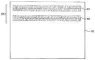
- FIG. 4shows, for example, portions of workpiece 170 that has been processed using mask 300 A of FIG. 3 a .
- Mask 300 Amay be rotated by about 90 degrees from the orientation shown in FIG. 3 a ).
- the portion showncorresponds to a row, for example, row 205 of workpiece 170 ( FIG. 2 ).
- Row 205 of processed workpiece 170includes recrystallized polycrystalline silicon linear regions or strips 401 , 402 , etc. Each of the linear strips is a result of irradiation by a radiation beamlet formed by a corresponding mask slit 301 , 302 , etc.
- the continuous extent of recrystallized silicon in the linear strips across row 205may be a consequence, for example, of a continuous movement of the stage 180 along path 230 under laser beam exposure ( FIG. 2 ).
- Strips 401 , 402may have a microstructure corresponding to the one shot exposure with colliding liquid/solid growth fronts in the center creating a long location-controlled grain boundary.
- the continuous extentmay be a result of closely spaced stepped movements of stage 180 along path 230 that are sufficiently overlapping to permit formation of a continuous recrystallized silicon strip, hi this alternative process, the microstructure of the recrystallized material may have long grains parallel to the scanning direction.
- the recrystallized polycrystalline silicone.g.
- strips 401 , 402 , etc.may have a generally uniform structure, which may be suitable for placement of the active region of one or more TFT devices.
- FIG. 5shows, exemplary results using mask 300 B of FIG. 3 b .
- Exemplary processed workpiece 170includes recrystallized polycrystalline silicon strips 501 , 502 , etc. Recrystallized polycrystalline silicon strips 501 , 502 , etc. like strips 401 and 402 may have a uniform crystalline structure, which is suitable for placement of the active regions of TFT devices.
- Strips 501 and 502 that are shown to be generally at right angles to each othermay correspond to radiation beamlets formed by orthogonal mask slits (e.g., FIG.
- the distinct geometrical orientation and physical separation of strips 501 and 502may be a consequence, for example, of physically separated exposure to laser radiation during the processing of workpiece 170 .
- the separated radiation exposuremay be achieved by stepped movement of stage 180 (e.g., along path 230 FIG. 2 ) during the processing. Additionally or alternatively, the separated exposure may be achieved by triggering laser 110 to generate radiation pulses at appropriate times and positions of stage 180 along path 230 while stage 180 and laser beam 164 are moved or scanned relative to each other at constant speeds.
- Computer 100may be used control the triggering of laser 110 at appropriate times and positions during the movement of stage 180 .
- Computer 100may act according to preprogrammed processing recipes that, for example, include geometrical design information for a workpiece-in-process.
- FIG. 6shows an exemplary design pattern 600 that may be used by computer 1000 to trigger laser 110 at appropriate times.
- Pattern 600may be a geometrical grid covering thin film silicon 175 /workpiece 170 .
- the gridmay, for example, be a rectangular x-y grid having co-ordinates (x 1 , x 2 , . . . etc.) and (y 1 , y 2 , . . . etc.).
- the grid spacingsmay be regular or irregular by design.
- Pattern 600may be laid out as physical fiducial marks (e.g., on the thin film workpiece) or may be a mathematical construct in the processing recipes.
- Computer 100may trigger laser 110 when stage 180 is at the grid coordinates (xi, yi). Computer 100 may do so in response, for example, to conventional position sensors or indicators, which may be deployed to sense the position of stage 180 .
- computer 100may trigger laser 110 at computed times, which are computed from parameters such as an initial stage position, and the speeds and direction of stage movements from the initial stage position.
- Computer 100also may be used advantageously to instruct laser 110 to emit radiation pulses at a variable rate, rather than at a usual even rate.
- the variable rate of pulse generationmay be used beneficially to accommodate changes in the speed of stage 180 , for example, as it accelerates or decelerates at the ends of paths 230 and the like.
Landscapes
- Engineering & Computer Science (AREA)
- Physics & Mathematics (AREA)
- Optics & Photonics (AREA)
- Microelectronics & Electronic Packaging (AREA)
- Condensed Matter Physics & Semiconductors (AREA)
- General Physics & Mathematics (AREA)
- Manufacturing & Machinery (AREA)
- Computer Hardware Design (AREA)
- Power Engineering (AREA)
- Chemical & Material Sciences (AREA)
- Crystallography & Structural Chemistry (AREA)
- Plasma & Fusion (AREA)
- Mechanical Engineering (AREA)
- Materials Engineering (AREA)
- Recrystallisation Techniques (AREA)
Abstract
Description
This application is a continuation of and claims priority under 35 U.S.C. §120 to U.S. patent application Ser. No. 13/592,843, entitled “A Single-Shot Semiconductor Processing System and Method Having Various Irradiation Patterns,” filed Aug. 23, 2012, which is a continuation of and claims priority under 35 U.S.C. §120 to U.S. patent application Ser. No. 13/019,042, entitled “A Single-Shot Semiconductor Processing System and Method Having Various Irradiation Patterns,” filed Feb. 1, 2011, which is a continuation of and claims priority under 35 U.S.C. §120 to U.S. patent application Ser. No. 12/708,307, filed Feb. 18, 2010, which is a continuation of and claims priority under 35 U.S.C. §120 to U.S. patent application Ser. No. 10/524,809, filed on Feb. 15, 2005, which is a national phase of International Patent Application No. PCT/US03/025947, filed Aug. 19, 2003, published on Feb. 26, 2004 as International Patent Publication No. WO 04/017381, which claims priority from U.S. Application No. 60/404,447, which was filed on Aug. 19, 2002, each of which are incorporated by reference in their entireties herein, and from which priority is claimed.
The present invention relates to semiconductor processing methods, and more particularly, to methods for making semiconductors materials in a form suitable for fabrication of thin-film transistor (“TFT”) devices.
Flat panel displays and other display units are used as visual imaging interfaces for the common and ubiquitous electronic devices and appliances such as computers, image sensors, and television sets. The displays are fabricated, for example, from thin films of liquid crystal and semiconductor material placed on glass or plastic substrates. Each display is composed of a grid (or matrix) of picture elements (“pixels”) in the liquid crystal layer. Thousands or millions of these pixels together create an image on the display. TFT devices fabricated in the semiconductor material layer are used as switches to individually turn each pixel “on” (light) or “off (dark). The semiconductor materials used for making the TFTs, traditionally, are amorphous or polycrystalline silicon thin films. These films are deposited on to the substrates by physical or chemical processes at relatively low deposition temperatures in consideration of the low melting temperatures of the substrate materials used (e.g., glass or plastic). The relatively low deposition temperatures degrade the crystallinity of the deposited silicon films and cause them to be amorphous or polycrystalline.
Unfortunately, the device characteristics of a TFT fabricated in a silicon thin film undesirably degrade generally in proportion to the non-crystallinity of the silicon thin film. For industrial TFT device applications, silicon thin films of good crystalline quality are desirable. The crystallinity of a thin film of silicon deposited at low temperatures on a substrate may be advantageously improved by laser annealing. Maegawa et al. U.S. Pat. No. 5,766,989, for example, describes the use of excimer laser annealing (“ELA”) to process amorphous silicon thin films deposited at low temperatures into polycrystalline silicon thin films for LCD applications. The conventional ELA processes, however, are not entirely satisfactory at least in part because the grain sizes in the annealed films are not sufficiently uniform for industrial use. The non-uniformity of grain size in the annealed films is related to the beam shape of the laser beam, which is used in the ELA process to scan the thin film.
Im et al. U.S. Pat. No. 6,573,531 and Im U.S. Pat. No. 6,322,625 (hereinafter “the '531 patent” and “the '625 patent”, respectively), both of which are incorporated by reference herein in their entireties, describe laser annealing apparatus and improved processes for making large grained polycrystalline or single crystal silicon structures. The laser annealing processes described in these patents involve controlled resolidification of target portions of a thin film that are melted by laser beam irradiation. The thin film may be a metal or semiconductor material (e.g., silicon). The fluence of a set of laser beam pulses incident on the silicon thin film is modulated to control the extent of melting of a target portion of a silicon thin film. Then, between the incident laser beam pulses, the position of the target portion is shifted by slight physical translation of the subject silicon thin film to encourage epitaxial lateral solidification. This so-called lateral solidification process advantageously propagates the crystal structure of the initially molten target portion into grains of large size. The apparatus used for the processing includes an excimer laser, beam fluence modulators, beam focussing optics, patterning masks, and a motorized translation stage for moving the subject thin film between or during the laser beam irradiation. (See e.g., the '531 patent,FIG. 1 , which is reproduced herein).
Consideration is now being given to ways of further improving laser annealing processes for semiconductor thin films, and in particular for recrystallization of thin films. Attention is directed towards apparatus and process techniques, with a view to both improve the annealing process, and to increase apparatus throughput for use, for example, in production of flat panel displays.
The present invention provides systems and methods for recrystallizing amorphous or polycrystalline semiconductor thin films to improve their crystalline quality and to thereby make them more suitable for device applications. The systems and processes are designed so that large surface area semiconductor thin films can be processed quickly.
Target areas of the semiconductor thin film may be intended for all or part semiconductor device structures. The target area may, for example, be intended for active regions of the semiconductor devices. The target areas are treated by laser beam irradiation to recrystallize them. The target areas are exposed to a laser beam having sufficient intensity or fluence to melt semiconductor material in the target areas. A one shot laser beam exposure may be used—the melted semiconductor material recrystallizes when the laser beam is turned off or moved away from the target area.
A large number of target areas in a region on the surface of the semiconductor thin film may be treated simultaneously by using laser radiation that is patterned. A projection mask can be deployed to suitably pattern the laser beam. The mask divides an incident laser beam into a number of beamlets that are incident on a corresponding number of target areas in a surface region of the semiconductor thin film. Each of the beamlets has sufficient fluence to melt the semiconductor material in target area on which it (beamlet) is incident. The dimensions of the beamlets may be chosen with consideration to the desired size of the target areas and the amount of semiconductor material that can be effectively recrystallized. Typical beamlet dimensions and corresponding target area dimensions may be of the order of the order of about 0.5 um to a few um.
An exemplary mask for patterning the laser beam radiation has a number of rectangular slits that are parallel to each other. Using this mask, an incident laser beam can be divided into a number of parallel beamlets. The target areas corresponding to these beamlets are distributed in the surface region in a similar parallel pattern. Another exemplary mask has a number of rectangular slits that are disposed in a rectangular pattern of sets of parallel and orthogonal slits. The slits may for example, be arranged in pairs along the sides of squares. Using this mask the resultant radiation beamlets and the corresponding target areas also are distributed in a similar rectangular pattern (e.g., in sets of parallel and orthogonal target areas).
The laser beam may be scanned or stepped across the surface of the semiconductor thin film to successively treat all regions of the surface with a repeating pattern of target areas. Conversely, the semiconductor thin film can be moved relative to a laser beam of fixed orientation for the same purpose. In one embodiment of the invention, a motorized linear translation stage is used to move the semiconductor thin film relative to the laser beam in linear X-Y paths so that all surface regions of the semiconductor thin film can be exposed to the laser beam irradiation. The movement of the stage during the process can be continuous across a width of the semiconductor thin film or can be stepped from one region to the next. For some device applications, the target areas in one region may be contiguous to target areas in the next region so that extended strips of semiconductor material can be recrystallized. The recrystallization contiguous target areas may benefit from sequential lateral solidification of the molten target areas. For other device applications, the target areas may be geometrically separate from target areas in the adjoining areas.
The generation of laser beam pulses for irradiation of the target areas may be synchronized with the movement of the linear translation stage so that the laser beam can be incident on designated target areas with geometric precision. The timing of the generated laser beam pulses may be indexed to the position of the translation stage, which supports the semiconductor thin film. The indexing may be occur in response to position sensors that indicate in real time the position of the stage, or may be based on computed co-ordinates of a geometrical grid overlaying the thin film semiconductor.
Further features of the invention, its nature, and various advantages will be more apparent from the following detailed description of the preferred embodiments and the accompanying drawings, wherein like reference characters represent like elements throughout, and in which:
The present invention provides processes and systems for recrystallization of semiconductor thin films by laser annealing. The processes for recrystallization of semiconductor thin films involve one-shot irradiation of regions of a semiconductor thin film workpiece to a laser beam. The systems direct a laser beam to a region or spot on the surface of the semiconductor thin film. The incident laser beam has sufficient intensity or fluence to melt targeted portions of the region or spot of the semiconductor thin film on which the laser beam is incident. After the targeted incident areas or portions are melted, the laser beam is moved or stepped to another region or spot on the semiconductor thin film. The molten semiconductor material recrystallizes when the incident laser beam is moved away. The dwell time of the laser beam on a spot on the semiconductor thin film may be sufficient small so that the recrystallization of an entire semiconductor thin film workpiece can be carried out quickly with high throughput rates.
In order that the invention herein described can be fully understood the subsequent description is set forth in the context of laser annealing of silicon thin films. The annealed silicon thin films may be intended for exemplary TFT device applications. It will, however, be understood that the invention is equally applicable to other types of materials and/or other types of device applications.
An embodiment of the present invention is described herein with reference toFIGS. 1-6 . Thin film silicon workpieces (see e.g.,workpiece 170, FIGS.2 and4-6) are used herein as illustrative workpieces.Workpiece 170 may, for example, be a film of amorphous or randomly expanding andcollimating lenses homogenizer 144,condenser lens 145, afield lens 148,eye piece 161, controllable shutter152, multi-element objective lens163), also may, for example, be any suitable commercially available optical components sold by the by Lambda Physik USA, or by other vendors.
The suitable optical components120-163 for shaping and directing the radiation beam may include amasking system 150. Maskingsystem 150 may be a projection masking system, which is used for patterning incident radiation (149) so that radiation beam (164) that is ultimately incident onworkpiece 170 is geometrically shaped or patterned.
Acomputer 100 may be linked tolaser 110,modulator 120,stage assembly 180 and other controllable components ofapparatus 1000.Computer 100 may be used to control the timing and fluence of the incident laser beam pulses and the relative movement of thestage assembly 180.Computer 100 may be programmed to controllably move stageassembly translation stage 180 in X, Y and Z directions.Workpiece 170 may be moved, for example, over predetermined distances in the X-Y plane and as well as in the Z direction in response to instruction fromcomputer 1000. In operation, the position ofworkpiece 170 relative to theincident radiation beam 164 may be continuously adjusted or intermittently reset during the single-shot laser annealing process at suitable times according to preprogrammed process recipes for single shot recrystallization ofworkpiece 170. The movement ofworkpiece 170 may be synchronized or co-ordinated with the timing of radiation beam pulses generated bylaser 100.
Inapparatus 1000, the movement ofstage assembly 180 translates theworkpiece 170 and the radiation beam (164) relative to each other. In the processing described herein the radiation beam (164) is held fixed in a position or orientation whilestage 180 is moved. Alternative configurations or arrangements of optical components may be used to moveincident radiation beam 164 andworkpiece 170 relative to each other along defined paths. For example, a computer-controlled beam steering mirror may be used to deflectradiation beam 164 whilestage 180 is held fixed in position. By such beam deflecting arrangements it may be possible to completely or partially dispense with the use of mechanical projection masks (e.g., masking system150) and instead use electronic or optical beam guiding mechanisms to scan or step selected portions ofworkpiece 170 at a rapid pace.
Usingapparatus 1000, sequential lateral solidification of molten semiconductor material may be achieved using, for example, the processes that involve incremental movement or shifting the position ofstage 180 between excimer laser pulses as described in the '531 patent. The movements ofstage 170 are small, so that the portions of the silicon thin film that are molten by sequential pulses are proximate to each other. The proximity of the two molten portions allows the first portion to recrystallize and propagate its crystal structure into the adjacent portion, which is melted by the next pulse.
In the single shot recrystallization processes described here,apparatus 1000 may be used to scan or step a laser beam across the surface of a semiconductor thin film by moving ofstage assembly 180. The laser beam has sufficient intensity or fluence to melt target areas in the regions or spots at which the laser beam pulses are incident. To process anentire workpiece 170,stage assembly 180 may be moved predetermined distances to cause the laser beam to move along paths across semiconductorthin film 175/workpiece 170.FIG. 2 also schematically showspaths incident radiation beam 164 as it is moved across the surface of theworkpiece 170.
The number of paths and their geometrical orientation may be determined by the cross sectional dimensions of the laser beam and the target area requirements of the circuit or device applications for whichworkpiece 170 is being processed. Accordingly, the surface of a semiconductorthin film 175/workpiece 170 may be partitioned in a geometric array of regions for generating processing recipes forcomputer 1000 or otherwise controlling the operation ofapparatus 1000.FIG. 2 shows an exemplary geometrical partitioning of the surface of a semiconductorthin film 175 onworkpiece 170. In the exemplary geometrical partitioning shown inFIG. 2 , the surface is divided into a number of rows (e.g.,205,206,207, etc.) each having a width W. The widths of rows W may be selected with consideration to the cross sectional width ofincident radiation beam 164. Each row contains one or more regions. As an illustrative numerical example,workpiece 170 may have x and y dimensions of about 30 cms and 40 cms, respectively. Each ofrows workpiece 170 can be divided into eighty (80) rows each with a length of about 30 cms in the X direction. Each row contains one or more regions whose combined length equals 30 cms (not shown).
The co-ordinates of each row may be stored incomputer 100 for use by the processing recipes.Computer 1000 may use the stored co-ordinates, for example, to compute the direction, timing and travel distances ofstage 180 during the processing. The co-ordinates also may be used, for example, to time the firing oflaser 110 so that designated regions of semiconductorthin film 175 are irradiated asstage 180 is moved.
The movement ofstage 180 may be conducted in a series of steps in an intermittent stop-and-go fashion, or continuously without pause until the center of the radiation beam is directed to apoint 240 near the right end ofrow 205.Path segments path 230 that may extend beyondedges 210′ and210″ ofworkpiece 170 topoints stage assembly 180 at the ends ofpath 230 and/or may be useful forreinitializing stage 180 position for movingstage 180 in another direction.Stage 180 may, for example, be moved in the negative Y direction frompoint 240, so that the center of the radiation beam tracespath 245 to point247 next to the right end ofrow 206 in preparation for treating the silicon material inrow 206. Frompoint 247 in manner similar to the movement alongpath 230 in row205 (but in the opposite direction),stage 180 is moved in the X direction so that the center of the radiation beam moves alongpath 255 irradiating thin film silicon material inrow 206. The movement may be continued till the center of radiation beam is incident atspot 265 that is near the left end ofrow 206.Path extensions path 255 that may extend beyondedges 210′ and210″ tospots stage 180 in the Y direction moves the center of the incident radiation beam alongpath 270 to apoint 272 next to row207. Then, the thin film silicon material inrow 207 may be processed by movingstage 180 in the negative X direction alongpath 275 and further toward theopposite side 210″ ofworkpiece 170. By continuing X and Y direction movements ofstage 180 in the manner described forrows thin film silicon 175 may be treated or irradiated. It will be understood that the particular directions or sequence of paths described above are used only for purposes of illustration, other directions or sequences may be used as appropriate.
In an operation ofapparatus 1000, siliconthin film 175 may be irradiated bybeam pulse 164 whose geometrical profile is defined by maskingsystem 150. Maskingsystem 150 may include suitable projection masks for this purpose. Maskingsystem 150 may cause a single incident radiation beam (e.g., beam149) incident on it to dissemble into a plurality of beamlets in a geometrical pattern. The beamlets irradiate a corresponding geometrical pattern of target areas in a region on the thin film silicon workpiece. The intensity of each of the beamlets may be chosen to be sufficient to induce complete melting of irradiated thin film silicon portions throughout their (film) thickness.
The projection masks may be made of suitable materials that block passage of radiation through undesired cross sectional areas ofbeam 149 but allow passage through desired areas. An exemplary projection mask may have a blocking/unblocking pattern of rectangular stripes or other suitable geometrical shapes which may be arranged in random or in geometrical patterens. The stripes may, for example, be placed in a parallel pattern as shown inFIG. 3 a, or in a mixed parallel and orthogonal pattern as shown inFIG. 3 b, or any other suitable pattern.
With reference toFIG. 3 a, exemplary mask300A includes beam-blocking portions310 which has a number of open ortransparent slits incident beam 149 through mask300A. In contrast, open ortransparent slits radiation beam 149 throughmask 300. Accordingly,radiation beam 164 exiting mask300 A has a cross section with a geometrical pattern corresponding to the parallel pattern of the plurality of open ortransparent slits system 150, mask300A may be used topattern radiation beam 164 that is incident on semiconductorthin film 175 as a collection of parallel rectangular-shaped beamlets. The beamlets irradiate a corresponding pattern of rectangular target areas in a region on the surface of the on semiconductorthin film 175. The beamlet dimensions may be selected with a view to promote recrystallization or lateral solidification of thin film silicon areas melted by a beamlet. For example, a side length of a beamlet may be chosen so that corresponding target areas in adjoining regions are contiguous. The size of the beamlets and the inter beamlet separation distances may be selected by suitable choice of the size and separation oftransparent slits transparent slits
It will be understood that the specific mask patterns shown inFIGS. 3 aand3bare exemplary. Any other suitable mask patterns may be used including, for example, the chevron shaped patterns described in the '625 patent. A particular mask pattern may be chosen in consideration of the desired placement of TFTs or other circuit or device elements in the semiconductor product for which the recrystallized thin film silicon material is intended.
It will be understood that the foregoing is only illustrative of the principles of the invention and that various modifications can be made by those skilled in the art without departing from the scope and spirit of the invention, which is limited only by the claims that follow.
Claims (14)
1. A method for crystallizing portions of a thin film, the method comprising:
providing the thin film;
patterning the thin film according to a pattern, wherein the pattern comprises a plurality of irradiation regions and a plurality of non-irradiation regions;
generating a radiation beam, wherein the radiation beam is incident on a first irradiation region of the thin film;
irradiating the first irradiation region of the thin film with a pulse of the radiation beam, wherein the radiation beam pulse has a fluence sufficient to partially melt the material in the first irradiation region on which it is incident, and wherein the partially molten material in the first irradiation region recrystallizes when it is no longer exposed to the radiation beam; and
continuously translating the thin film relative to the radiation beam such that a second irradiation region of the surface of the thin film is irradiated with a second radiation beam pulse having a fluence sufficient to partially melt the material in the second irradiation region on which it is incident, and wherein the partially molten material in the second irradiation region recrystallizes when it is no longer exposed to the radiation beam.
2. The method ofclaim 1 , wherein the plurality of irradiation regions comprises a semiconductor material.
3. The method ofclaim 1 , wherein the thin film comprises silicon.
4. The method ofclaim 1 , wherein the radiation beam has a cross section on the order of 10 microns.
5. The method ofclaim 1 , wherein the radiation beam has a cross section on the order of 100 microns.
6. The method ofclaim 1 , wherein the first irradiation region is adjacent to a first non-irradiation region.
7. The method ofclaim 6 , wherein the second irradiation region is adjacent to a second non-irradiation region.
8. A system for recrystallizing a semiconductor thin film using a controllable radiation beam source, comprising:
a processing arrangement adapted to operatively couple to the radiation beam source, wherein the processing arrangement is configured to:
pattern the thin film according to a pattern, wherein the pattern comprises a plurality of irradiation regions and a plurality of non-irradiation regions;
generate a radiation beam, wherein the radiation beam is incident on a first irradiation region of the thin film;
irradiate the first irradiation region of the thin film with a pulse of the radiation beam, wherein the radiation beam pulse has a fluence sufficient to partially melt the material in the first irradiation region on which it is incident, and wherein the partially molten material in the first irradiation region recrystallizes when it is no longer exposed to the radiation beam; and
continuously translate the thin film relative to the radiation beam such that a second irradiation region of the surface of the thin film is irradiated with a second radiation beam pulse having a fluence sufficient to partially melt the material in the second irradiation region on which it is incident, and wherein the partially molten material in the second irradiation region recrystallizes when it is no longer exposed to the radiation beam.
9. The system ofclaim 8 , wherein the plurality of irradiation regions comprises a semiconductor material.
10. The system ofclaim 8 , wherein the thin film comprises silicon.
11. The system ofclaim 8 , wherein the radiation beam has a cross section on the order of 10 microns.
12. The system ofclaim 8 , wherein the radiation beam has a cross section on the order of 100 microns.
13. The system ofclaim 8 , wherein the first irradiation region is adjacent to a first non-irradiation region.
14. The system ofclaim 13 , wherein the second irradiation region is adjacent to a second non-irradiation region.
Priority Applications (1)
| Application Number | Priority Date | Filing Date | Title |
|---|---|---|---|
| US13/956,802US8883656B2 (en) | 2002-08-19 | 2013-08-01 | Single-shot semiconductor processing system and method having various irradiation patterns |
Applications Claiming Priority (7)
| Application Number | Priority Date | Filing Date | Title |
|---|---|---|---|
| US40444702P | 2002-08-19 | 2002-08-19 | |
| US10/524,809US7718517B2 (en) | 2002-08-19 | 2003-08-19 | Single-shot semiconductor processing system and method having various irradiation patterns |
| PCT/US2003/025947WO2004017380A2 (en) | 2002-08-19 | 2003-08-19 | A single-shot semiconductor processing system and method having various irradiation patterns |
| US12/708,307US7906414B2 (en) | 2002-08-19 | 2010-02-18 | Single-shot semiconductor processing system and method having various irradiation patterns |
| US13/019,042US8479681B2 (en) | 2002-08-19 | 2011-02-01 | Single-shot semiconductor processing system and method having various irradiation patterns |
| US13/592,843US8507368B2 (en) | 2002-08-19 | 2012-08-23 | Single-shot semiconductor processing system and method having various irradiation patterns |
| US13/956,802US8883656B2 (en) | 2002-08-19 | 2013-08-01 | Single-shot semiconductor processing system and method having various irradiation patterns |
Related Parent Applications (1)
| Application Number | Title | Priority Date | Filing Date |
|---|---|---|---|
| US13/592,843ContinuationUS8507368B2 (en) | 2002-08-19 | 2012-08-23 | Single-shot semiconductor processing system and method having various irradiation patterns |
Publications (2)
| Publication Number | Publication Date |
|---|---|
| US20130316548A1 US20130316548A1 (en) | 2013-11-28 |
| US8883656B2true US8883656B2 (en) | 2014-11-11 |
Family
ID=31888365
Family Applications (5)
| Application Number | Title | Priority Date | Filing Date |
|---|---|---|---|
| US10/524,809Expired - Fee RelatedUS7718517B2 (en) | 2002-08-19 | 2003-08-19 | Single-shot semiconductor processing system and method having various irradiation patterns |
| US12/708,307Expired - Fee RelatedUS7906414B2 (en) | 2002-08-19 | 2010-02-18 | Single-shot semiconductor processing system and method having various irradiation patterns |
| US13/019,042Expired - Fee RelatedUS8479681B2 (en) | 2002-08-19 | 2011-02-01 | Single-shot semiconductor processing system and method having various irradiation patterns |
| US13/592,843Expired - Fee RelatedUS8507368B2 (en) | 2002-08-19 | 2012-08-23 | Single-shot semiconductor processing system and method having various irradiation patterns |
| US13/956,802Expired - LifetimeUS8883656B2 (en) | 2002-08-19 | 2013-08-01 | Single-shot semiconductor processing system and method having various irradiation patterns |
Family Applications Before (4)
| Application Number | Title | Priority Date | Filing Date |
|---|---|---|---|
| US10/524,809Expired - Fee RelatedUS7718517B2 (en) | 2002-08-19 | 2003-08-19 | Single-shot semiconductor processing system and method having various irradiation patterns |
| US12/708,307Expired - Fee RelatedUS7906414B2 (en) | 2002-08-19 | 2010-02-18 | Single-shot semiconductor processing system and method having various irradiation patterns |
| US13/019,042Expired - Fee RelatedUS8479681B2 (en) | 2002-08-19 | 2011-02-01 | Single-shot semiconductor processing system and method having various irradiation patterns |
| US13/592,843Expired - Fee RelatedUS8507368B2 (en) | 2002-08-19 | 2012-08-23 | Single-shot semiconductor processing system and method having various irradiation patterns |
Country Status (7)
| Country | Link |
|---|---|
| US (5) | US7718517B2 (en) |
| JP (1) | JP2006512749A (en) |
| KR (1) | KR20050047103A (en) |
| CN (1) | CN1757093A (en) |
| AU (1) | AU2003258289A1 (en) |
| TW (1) | TWI331803B (en) |
| WO (1) | WO2004017380A2 (en) |
Cited By (1)
| Publication number | Priority date | Publication date | Assignee | Title |
|---|---|---|---|---|
| US20190015929A1 (en)* | 2015-12-30 | 2019-01-17 | Shanghai Micro Electronics Equipment (Group) Co., Ltd. | Laser annealing device and annealing method therefor |
Families Citing this family (57)
| Publication number | Priority date | Publication date | Assignee | Title |
|---|---|---|---|---|
| US6555449B1 (en) | 1996-05-28 | 2003-04-29 | Trustees Of Columbia University In The City Of New York | Methods for producing uniform large-grained and grain boundary location manipulated polycrystalline thin film semiconductors using sequential lateral solidfication |
| US6830993B1 (en) | 2000-03-21 | 2004-12-14 | The Trustees Of Columbia University In The City Of New York | Surface planarization of thin silicon films during and after processing by the sequential lateral solidification method |
| KR100854834B1 (en) | 2000-10-10 | 2008-08-27 | 더 트러스티스 오브 컬럼비아 유니버시티 인 더 시티 오브 뉴욕 | Method and apparatus for processing thin metal layers |
| US6961117B2 (en) | 2000-11-27 | 2005-11-01 | The Trustees Of Columbia University In The City Of New York | Process and mask projection system for laser crystallization processing of semiconductor film regions on a substrate |
| KR100400510B1 (en)* | 2000-12-28 | 2003-10-08 | 엘지.필립스 엘시디 주식회사 | A machine for Si crystallization and method of crystallizing Si |
| TW556350B (en) | 2001-08-27 | 2003-10-01 | Univ Columbia | A method to increase device-to-device uniformity for polycrystalline thin-film transistors by deliberately mis-aligning the microstructure relative to the channel region |
| AU2003220611A1 (en) | 2002-04-01 | 2003-10-20 | The Trustees Of Columbia University In The City Of New York | Method and system for providing a thin film |
| WO2004017380A2 (en) | 2002-08-19 | 2004-02-26 | The Trustees Of Columbia University In The City Of New York | A single-shot semiconductor processing system and method having various irradiation patterns |
| KR101131040B1 (en) | 2002-08-19 | 2012-03-30 | 더 트러스티스 오브 콜롬비아 유니버시티 인 더 시티 오브 뉴욕 | Process and system for laser crystallization processing of film regions on a substrate to minimize edge areas, and structure of such film regions |
| CN100447941C (en) | 2002-08-19 | 2008-12-31 | 纽约市哥伦比亚大学托管会 | A method and system for processing thin film samples and its thin film domain structure |
| US7300858B2 (en) | 2002-08-19 | 2007-11-27 | The Trustees Of Columbia University In The City Of New York | Laser crystallization and selective patterning using multiple beamlets |
| WO2004075263A2 (en) | 2003-02-19 | 2004-09-02 | The Trustees Of Columbia University In The City Of New York | System and process for processing a plurality of semiconductor thin films which are crystallized using sequential lateral solidification techniques |
| KR100546711B1 (en)* | 2003-08-18 | 2006-01-26 | 엘지.필립스 엘시디 주식회사 | Laser irradiation apparatus and silicon crystallization method using the same |
| WO2005029546A2 (en) | 2003-09-16 | 2005-03-31 | The Trustees Of Columbia University In The City Of New York | Method and system for providing a continuous motion sequential lateral solidification for reducing or eliminating artifacts, and a mask for facilitating such artifact reduction/elimination |
| TWI359441B (en) | 2003-09-16 | 2012-03-01 | Univ Columbia | Processes and systems for laser crystallization pr |
| US7364952B2 (en)* | 2003-09-16 | 2008-04-29 | The Trustees Of Columbia University In The City Of New York | Systems and methods for processing thin films |
| WO2005029547A2 (en) | 2003-09-16 | 2005-03-31 | The Trustees Of Columbia University In The City Of New York | Enhancing the width of polycrystalline grains with mask |
| US7318866B2 (en)* | 2003-09-16 | 2008-01-15 | The Trustees Of Columbia University In The City Of New York | Systems and methods for inducing crystallization of thin films using multiple optical paths |
| TWI351713B (en) | 2003-09-16 | 2011-11-01 | Univ Columbia | Method and system for providing a single-scan, con |
| US7164152B2 (en) | 2003-09-16 | 2007-01-16 | The Trustees Of Columbia University In The City Of New York | Laser-irradiated thin films having variable thickness |
| KR100531416B1 (en)* | 2003-09-17 | 2005-11-29 | 엘지.필립스 엘시디 주식회사 | Device used in Sequential Lateral Solidification and Method for Crystallizing Silicon with the same |
| WO2005034193A2 (en)* | 2003-09-19 | 2005-04-14 | The Trustees Of Columbia University In The City Ofnew York | Single scan irradiation for crystallization of thin films |
| US7329884B2 (en)* | 2004-11-08 | 2008-02-12 | Nikon Corporation | Exposure apparatus and exposure method |
| US7645337B2 (en)* | 2004-11-18 | 2010-01-12 | The Trustees Of Columbia University In The City Of New York | Systems and methods for creating crystallographic-orientation controlled poly-silicon films |
| US8221544B2 (en) | 2005-04-06 | 2012-07-17 | The Trustees Of Columbia University In The City Of New York | Line scan sequential lateral solidification of thin films |
| TWI524384B (en)* | 2005-08-16 | 2016-03-01 | 紐約市哥倫比亞大學理事會 | High-capacity crystallization of the film layer |
| US8598588B2 (en)* | 2005-12-05 | 2013-12-03 | The Trustees Of Columbia University In The City Of New York | Systems and methods for processing a film, and thin films |
| JP2007165716A (en)* | 2005-12-15 | 2007-06-28 | Advanced Lcd Technologies Development Center Co Ltd | Laser crystallization apparatus and crystallization method |
| JP4956987B2 (en)* | 2005-12-16 | 2012-06-20 | 株式会社島津製作所 | Laser crystallization apparatus and crystallization method |
| TW200942935A (en) | 2007-09-21 | 2009-10-16 | Univ Columbia | Collections of laterally crystallized semiconductor islands for use in thin film transistors and systems and methods for making same |
| JP5385289B2 (en) | 2007-09-25 | 2014-01-08 | ザ トラスティーズ オブ コロンビア ユニヴァーシティ イン ザ シティ オブ ニューヨーク | Method for producing high uniformity in thin film transistor devices fabricated on laterally crystallized thin films |
| WO2009067688A1 (en) | 2007-11-21 | 2009-05-28 | The Trustees Of Columbia University In The City Of New York | Systems and methods for preparing epitaxially textured polycrystalline films |
| WO2009067687A1 (en)* | 2007-11-21 | 2009-05-28 | The Trustees Of Columbia University In The City Of New York | Systems and methods for preparation of epitaxially textured thick films |
| US8012861B2 (en) | 2007-11-21 | 2011-09-06 | The Trustees Of Columbia University In The City Of New York | Systems and methods for preparing epitaxially textured polycrystalline films |
| US20110175099A1 (en)* | 2008-02-29 | 2011-07-21 | The Trustees Of Columbia University In The City Of New York | Lithographic method of making uniform crystalline si films |
| WO2009111326A2 (en)* | 2008-02-29 | 2009-09-11 | The Trustees Of Columbia University In The City Of New York | Flash light annealing for thin films |
| US8569155B2 (en)* | 2008-02-29 | 2013-10-29 | The Trustees Of Columbia University In The City Of New York | Flash lamp annealing crystallization for large area thin films |
| US8193071B2 (en)* | 2008-03-11 | 2012-06-05 | Semiconductor Energy Laboratory Co., Ltd. | Method for manufacturing semiconductor device |
| US8598050B2 (en)* | 2008-06-26 | 2013-12-03 | Ihi Corporation | Laser annealing method and apparatus |
| JP5540476B2 (en)* | 2008-06-30 | 2014-07-02 | 株式会社Ihi | Laser annealing equipment |
| JP2012508985A (en) | 2008-11-14 | 2012-04-12 | ザ トラスティーズ オブ コロンビア ユニヴァーシティ イン ザ シティ オブ ニューヨーク | System and method for thin film crystallization |
| US9087696B2 (en) | 2009-11-03 | 2015-07-21 | The Trustees Of Columbia University In The City Of New York | Systems and methods for non-periodic pulse partial melt film processing |
| US8440581B2 (en)* | 2009-11-24 | 2013-05-14 | The Trustees Of Columbia University In The City Of New York | Systems and methods for non-periodic pulse sequential lateral solidification |
| US9646831B2 (en)* | 2009-11-03 | 2017-05-09 | The Trustees Of Columbia University In The City Of New York | Advanced excimer laser annealing for thin films |
| US9075409B2 (en) | 2011-06-28 | 2015-07-07 | Global Filtration Systems | Apparatus and method for forming three-dimensional objects using linear solidification |
| EP2726264B1 (en) | 2011-06-28 | 2016-11-23 | Global Filtration Systems, A DBA of Gulf Filtration Systems Inc. | Apparatus for forming three-dimensional objects using an ultraviolet laser diode |
| DE102012012088A1 (en)* | 2012-06-18 | 2013-12-19 | Jean-Paul Theis | Process for producing semiconductor thin films on foreign substrates |
| WO2014165643A2 (en) | 2013-04-04 | 2014-10-09 | Global Filtration Systems, A Dba Of Gulf Filtration Systems Inc. | Apparatus and method for forming three-dimensional objects using linear solidification with travel axis correction and power control |
| US20150102531A1 (en) | 2013-10-11 | 2015-04-16 | Global Filtration Systems, A Dba Of Gulf Filtration Systems Inc. | Apparatus and method for forming three-dimensional objects using a curved build platform |
| US20150146179A1 (en)* | 2013-11-25 | 2015-05-28 | Takao Utsumi | Low energy electron beam lithography |
| US9586364B2 (en) | 2013-11-27 | 2017-03-07 | Global Filtration Systems | Apparatus and method for forming three-dimensional objects using linear solidification with contourless object data |
| US9527244B2 (en) | 2014-02-10 | 2016-12-27 | Global Filtration Systems | Apparatus and method for forming three-dimensional objects from solidifiable paste |
| WO2015126461A1 (en) | 2014-02-20 | 2015-08-27 | Global Filtration Systems, A Dba Of Gulf Filtration Systems Inc. | Apparatus and method for forming three-dimensional objects using a tilting solidification substrate |
| US10144205B2 (en) | 2014-02-20 | 2018-12-04 | Global Filtration Systems | Apparatus and method for forming three-dimensional objects using a tilting solidification substrate |
| US11104117B2 (en) | 2014-02-20 | 2021-08-31 | Global Filtration Systems | Apparatus and method for forming three-dimensional objects using a tilting solidification substrate |
| JP6027150B2 (en) | 2014-06-24 | 2016-11-16 | 内海 孝雄 | Low energy electron beam lithography |
| US9902112B2 (en) | 2015-04-07 | 2018-02-27 | Global Filtration Systems | Apparatus and method for forming three-dimensional objects using linear solidification and a vacuum blade |
Citations (299)
| Publication number | Priority date | Publication date | Assignee | Title |
|---|---|---|---|---|
| US3632205A (en) | 1969-01-29 | 1972-01-04 | Thomson Csf | Electro-optical image-tracing systems, particularly for use with laser beams |
| US4234358A (en) | 1979-04-05 | 1980-11-18 | Western Electric Company, Inc. | Patterned epitaxial regrowth using overlapping pulsed irradiation |
| US4309225A (en) | 1979-09-13 | 1982-01-05 | Massachusetts Institute Of Technology | Method of crystallizing amorphous material with a moving energy beam |
| JPS5727035Y1 (en) | 1972-09-08 | 1982-06-11 | ||
| US4382658A (en) | 1980-11-24 | 1983-05-10 | Hughes Aircraft Company | Use of polysilicon for smoothing of liquid crystal MOS displays |
| US4456371A (en) | 1982-06-30 | 1984-06-26 | International Business Machines Corporation | Optical projection printing threshold leveling arrangement |
| US4514895A (en) | 1983-04-20 | 1985-05-07 | Mitsubishi Denki Kabushiki Kaisha | Method of forming field-effect transistors using selectively beam-crystallized polysilicon channel regions |
| US4560880A (en) | 1983-09-19 | 1985-12-24 | Varian Associates, Inc. | Apparatus for positioning a workpiece in a localized vacuum processing system |
| US4639277A (en) | 1984-07-02 | 1987-01-27 | Eastman Kodak Company | Semiconductor material on a substrate, said substrate comprising, in order, a layer of organic polymer, a layer of metal or metal alloy and a layer of dielectric material |
| JPS62181419A (en) | 1986-02-05 | 1987-08-08 | Nec Corp | Recrystallization method of polycrystalline silicon |
| US4691983A (en) | 1983-10-14 | 1987-09-08 | Hitachi, Ltd. | Optical waveguide and method for making the same |
| JPS62216320A (en) | 1986-03-18 | 1987-09-22 | Fujitsu Ltd | Laser annealing equipment |
| JPS62160781U (en) | 1986-04-01 | 1987-10-13 | ||
| US4727047A (en) | 1980-04-10 | 1988-02-23 | Massachusetts Institute Of Technology | Method of producing sheets of crystalline material |
| US4758533A (en) | 1987-09-22 | 1988-07-19 | Xmr Inc. | Laser planarization of nonrefractory metal during integrated circuit fabrication |
| US4793694A (en) | 1986-04-23 | 1988-12-27 | Quantronix Corporation | Method and apparatus for laser beam homogenization |
| US4800179A (en) | 1986-06-13 | 1989-01-24 | Fujitsu Limited | Method for fabricating semiconductor device |
| JPH0123920Y2 (en) | 1982-02-16 | 1989-07-20 | ||
| US4855014A (en) | 1986-01-24 | 1989-08-08 | Sharp Kabushiki Kaisha | Method for manufacturing semiconductor devices |
| US4870031A (en) | 1985-10-07 | 1989-09-26 | Kozo Iizuka, Director General, Agency Of Industrial Science And Technology | Method of manufacturing a semiconductor device |
| JPH01256114A (en) | 1988-04-06 | 1989-10-12 | Hitachi Ltd | Laser annealing method |
| US4940505A (en) | 1988-12-02 | 1990-07-10 | Eaton Corporation | Method for growing single crystalline silicon with intermediate bonding agent and combined thermal and photolytic activation |
| US4970546A (en) | 1988-04-07 | 1990-11-13 | Nikon Corporation | Exposure control device |
| US4976809A (en) | 1989-12-18 | 1990-12-11 | North American Philips Corp, Signetics Division | Method of forming an aluminum conductor with highly oriented grain structure |
| US5032233A (en) | 1990-09-05 | 1991-07-16 | Micron Technology, Inc. | Method for improving step coverage of a metallization layer on an integrated circuit by use of a high melting point metal as an anti-reflective coating during laser planarization |
| US5061655A (en) | 1990-02-16 | 1991-10-29 | Mitsubishi Denki Kabushiki Kaisha | Method of producing SOI structures |
| US5076667A (en) | 1990-01-29 | 1991-12-31 | David Sarnoff Research Center, Inc. | High speed signal and power supply bussing for liquid crystal displays |
| JPH0433327A (en) | 1990-05-30 | 1992-02-04 | Kyocera Corp | Method for forming semiconductor crystallized film |
| USRE33836E (en) | 1987-10-22 | 1992-03-03 | Mrs Technology, Inc. | Apparatus and method for making large area electronic devices, such as flat panel displays and the like, using correlated, aligned dual optical systems |
| JPH04167419A (en) | 1990-10-31 | 1992-06-15 | Toshiba Corp | Laser exposure equipment |
| US5145808A (en) | 1990-08-22 | 1992-09-08 | Sony Corporation | Method of crystallizing a semiconductor thin film |
| US5148379A (en) | 1988-12-02 | 1992-09-15 | Hitachi Ltd. | Method for automatically generating a simulation program for a physical phenomenon governed by a partial differential equation, with simplified input procedure and debug procedure |
| JPH04279064A (en) | 1991-03-07 | 1992-10-05 | Sharp Corp | Display device |
| JPH04282869A (en) | 1991-03-11 | 1992-10-07 | G T C:Kk | Method for manufacturing a thin film semiconductor device and apparatus for carrying out the method |
| US5173441A (en) | 1991-02-08 | 1992-12-22 | Micron Technology, Inc. | Laser ablation deposition process for semiconductor manufacture |
| US5204659A (en) | 1987-11-13 | 1993-04-20 | Honeywell Inc. | Apparatus and method for providing a gray scale in liquid crystal flat panel displays |
| US5233207A (en) | 1990-06-25 | 1993-08-03 | Nippon Steel Corporation | MOS semiconductor device formed on insulator |
| US5247375A (en) | 1990-03-09 | 1993-09-21 | Hitachi, Ltd. | Display device, manufacturing method thereof and display panel |
| US5281840A (en) | 1991-03-28 | 1994-01-25 | Honeywell Inc. | High mobility integrated drivers for active matrix displays |
| US5285236A (en) | 1992-09-30 | 1994-02-08 | Kanti Jain | Large-area, high-throughput, high-resolution projection imaging system |
| US5291240A (en) | 1992-10-27 | 1994-03-01 | Anvik Corporation | Nonlinearity-compensated large-area patterning system |
| US5294811A (en) | 1990-11-30 | 1994-03-15 | Hitachi, Ltd. | Thin film semiconductor device having inverted stagger structure, and device having such semiconductor device |
| JPH0611729Y2 (en) | 1986-03-28 | 1994-03-30 | 大和工業株式会社 | Movable location pin device |
| US5304357A (en) | 1991-05-15 | 1994-04-19 | Ricoh Co. Ltd. | Apparatus for zone melting recrystallization of thin semiconductor film |
| US5334892A (en) | 1992-12-22 | 1994-08-02 | Anorad Corporation | Positioning device for planar positioning |
| US5338959A (en) | 1992-03-30 | 1994-08-16 | Samsung Electronics Co., Ltd. | Thin film transistor with three dimensional multichannel structure |
| JPH06260502A (en) | 1993-03-04 | 1994-09-16 | Seiko Epson Corp | Manufacture of active matrix substrate |
| US5373803A (en) | 1991-10-04 | 1994-12-20 | Sony Corporation | Method of epitaxial growth of semiconductor |
| US5395481A (en) | 1993-10-18 | 1995-03-07 | Regents Of The University Of California | Method for forming silicon on a glass substrate |
| US5409867A (en) | 1993-06-16 | 1995-04-25 | Fuji Electric Co., Ltd. | Method of producing polycrystalline semiconductor thin film |
| US5413958A (en) | 1992-11-16 | 1995-05-09 | Tokyo Electron Limited | Method for manufacturing a liquid crystal display substrate |
| US5417897A (en) | 1993-05-10 | 1995-05-23 | Hewlett-Packard Company | Method for forming tapered inkjet nozzles |
| EP0655774A2 (en) | 1993-11-02 | 1995-05-31 | Sony Corporation | Method of forming polycrystalline silicon layer and surface treatment apparatus therefor |
| US5436095A (en) | 1991-07-11 | 1995-07-25 | Hitachi, Ltd. | Manufacturing method or an exposing method for a semiconductor device for a semiconductor integrated circuit device and a mask used therefor |
| US5453594A (en) | 1993-10-06 | 1995-09-26 | Electro Scientific Industries, Inc. | Radiation beam position and emission coordination system |
| US5456763A (en) | 1994-03-29 | 1995-10-10 | The Regents Of The University Of California | Solar cells utilizing pulsed-energy crystallized microcrystalline/polycrystalline silicon |
| EP0681316A2 (en) | 1994-05-02 | 1995-11-08 | Sony Corporation | Method of processing a thin film on a substrate for display |
| US5466908A (en) | 1992-02-18 | 1995-11-14 | Fujitsu Limited | Method and apparatus for cutting patterns of printed wiring boards and method and apparatus for cleaning printed wiring boards |
| US5496768A (en) | 1993-12-03 | 1996-03-05 | Casio Computer Co., Ltd. | Method of manufacturing polycrystalline silicon thin film |
| JPH0878330A (en) | 1994-06-27 | 1996-03-22 | Casio Comput Co Ltd | Method for manufacturing polycrystalline silicon thin film |
| US5512494A (en) | 1993-11-29 | 1996-04-30 | Nec Corporation | Method for manufacturing a thin film transistor having a forward staggered structure |
| US5523193A (en) | 1988-05-31 | 1996-06-04 | Texas Instruments Incorporated | Method and apparatus for patterning and imaging member |
| US5534716A (en) | 1993-08-27 | 1996-07-09 | Semiconductor Energy Laboratory Co., Ltd. | Semiconductor device having transistors with different orientations of crystal channel growth with respect to current carrier direction |
| US5591668A (en) | 1994-03-14 | 1997-01-07 | Matsushita Electric Industrial Co., Ltd. | Laser annealing method for a semiconductor thin film |
| JPH097968A (en) | 1995-06-23 | 1997-01-10 | Mitsubishi Electric Corp | Laser light irradiation method and laser light irradiation device |
| US5596283A (en) | 1991-06-26 | 1997-01-21 | Digital Equipment Corporation | Continuous motion electrical circuit interconnect test method and apparatus |
| US5614426A (en) | 1993-08-10 | 1997-03-25 | Semiconductor Energy Laboratory Co., Ltd. | Method of manufacturing semiconductor device having different orientations of crystal channel growth |
| US5614421A (en) | 1994-03-11 | 1997-03-25 | United Microelectronics Corp. | Method of fabricating junction termination extension structure for high-voltage diode devices |
| US5620910A (en) | 1994-06-23 | 1997-04-15 | Semiconductor Energy Laboratory Co., Ltd. | Method for producing semiconductor device with a gate insulating film consisting of silicon oxynitride |
| JPH09171971A (en) | 1995-12-21 | 1997-06-30 | Japan Steel Works Ltd:The | Laser annealing equipment |
| JPH09270393A (en) | 1996-03-29 | 1997-10-14 | Sanyo Electric Co Ltd | Laser light irradiation device |
| US5683935A (en) | 1995-02-28 | 1997-11-04 | Fuji Xerox Co., Ltd. | Method of growing semiconductor crystal |
| US5710050A (en) | 1994-08-25 | 1998-01-20 | Sharp Kabushiki Kaisha | Method for fabricating a semiconductor device |
| US5721606A (en) | 1995-09-07 | 1998-02-24 | Jain; Kanti | Large-area, high-throughput, high-resolution, scan-and-repeat, projection patterning system employing sub-full mask |
| US5736709A (en) | 1996-08-12 | 1998-04-07 | Armco Inc. | Descaling metal with a laser having a very short pulse width and high average power |
| US5742426A (en) | 1995-05-25 | 1998-04-21 | York; Kenneth K. | Laser beam treatment pattern smoothing device and laser beam treatment pattern modulator |
| US5756364A (en) | 1994-11-29 | 1998-05-26 | Semiconductor Energy Laboratory Co., Ltd. | Laser processing method of semiconductor device using a catalyst |
| WO1998024118A1 (en) | 1996-11-28 | 1998-06-04 | Philips Electronics N.V. | Electronic device manufacture by energy beam crystallisation |
| US5766989A (en) | 1994-12-27 | 1998-06-16 | Matsushita Electric Industrial Co., Ltd. | Method for forming polycrystalline thin film and method for fabricating thin-film transistor |
| US5767003A (en) | 1995-09-19 | 1998-06-16 | Sony Corporation | Thin film semiconductor device manufacturing method |
| JPH10189998A (en) | 1996-12-20 | 1998-07-21 | Sony Corp | Display thin film semiconductor device and method of manufacturing the same |
| JPH10244390A (en) | 1997-03-04 | 1998-09-14 | Toshiba Corp | Laser processing method and apparatus |
| US5817548A (en) | 1995-11-10 | 1998-10-06 | Sony Corporation | Method for fabricating thin film transistor device |
| US5844588A (en) | 1995-01-11 | 1998-12-01 | Texas Instruments Incorporated | DMD modulated continuous wave light source for xerographic printer |
| US5858807A (en) | 1996-01-17 | 1999-01-12 | Kabushiki Kaisha Toshiba | Method of manufacturing liquid crystal display device |
| US5861991A (en) | 1996-12-19 | 1999-01-19 | Xerox Corporation | Laser beam conditioner using partially reflective mirrors |
| JPH1164883A (en) | 1997-08-12 | 1999-03-05 | Toshiba Corp | Method and apparatus for manufacturing polycrystalline semiconductor thin film |
| US5893990A (en) | 1995-05-31 | 1999-04-13 | Semiconductor Energy Laboratory Co. Ltd. | Laser processing method |
| WO1999031719A1 (en) | 1997-12-17 | 1999-06-24 | Matsushita Electric Industrial Co., Ltd. | Semiconductor thin film, method of producing the same, apparatus for producing the same, semiconductor device and method of producing the same |
| US5948291A (en) | 1997-04-29 | 1999-09-07 | General Scanning, Inc. | Laser beam distributor and computer program for controlling the same |
| US5960323A (en) | 1996-06-20 | 1999-09-28 | Sanyo Electric Co., Ltd. | Laser anneal method for a semiconductor device |
| JPH11281997A (en) | 1998-03-26 | 1999-10-15 | Toshiba Corp | Circuit board, manufacturing method thereof and liquid crystal display device |
| JPH11297852A (en) | 1998-04-14 | 1999-10-29 | Sony Corp | Semiconductor device and manufacturing method thereof |
| US5981974A (en) | 1996-09-30 | 1999-11-09 | Sharp Kabushiki Kaisha | Semiconductor device and method for fabricating the same |
| US5986807A (en) | 1997-01-13 | 1999-11-16 | Xerox Corporation | Single binary optical element beam homogenizer |
| JPH11330000A (en) | 1998-05-13 | 1999-11-30 | Matsushita Electric Ind Co Ltd | Laser annealing method for non-single crystal thin film |
| US6002523A (en) | 1997-09-30 | 1999-12-14 | Semiconductor Energy Laboratory Co., Ltd. | Laser illumination method |
| GB2338343A (en) | 1998-06-09 | 1999-12-15 | Lg Lcd Inc | Method for fabricating thin film transistor |
| GB2338342A (en) | 1998-06-09 | 1999-12-15 | Lg Lcd Inc | Method for crystallizing amorphous silicon layer and method for fabricating tft |
| GB2338597A (en) | 1998-06-09 | 1999-12-22 | Lg Lcd Inc | Method of forming a thin film transistor by laser induced crystallisation in a predetermined direction |
| US6014944A (en) | 1997-09-19 | 2000-01-18 | The United States Of America As Represented By The Secretary Of The Navy | Apparatus for improving crystalline thin films with a contoured beam pulsed laser |
| US6020224A (en) | 1997-06-19 | 2000-02-01 | Sony Corporation | Method for making thin film transistor |
| DE19839718A1 (en) | 1998-09-01 | 2000-03-02 | Strunk Horst P | Laser crystallization or crystal structure alteration of amorphous or polycrystalline semiconductor layers comprises paired laser pulse irradiation for extended melt time while maintaining a low substrate temperature |
| WO2000014784A1 (en) | 1998-09-04 | 2000-03-16 | Koninklijke Philips Electronics N.V. | Double-pulse laser crystallisation of thin semiconductor films |
| US6045980A (en) | 1995-09-29 | 2000-04-04 | Leybold Systems Gmbh | Optical digital media recording and reproduction system |
| JP2000505241A (en) | 1996-05-28 | 2000-04-25 | ザ トラスティース オブ コロンビア ユニヴァーシティ イン ザ シティ オブ ニューヨーク | Crystallization of semiconductor film region on substrate and device manufactured by this method |
| US6072631A (en) | 1998-07-09 | 2000-06-06 | 3M Innovative Properties Company | Diffractive homogenizer with compensation for spatial coherence |
| US6081381A (en) | 1998-10-26 | 2000-06-27 | Polametrics, Inc. | Apparatus and method for reducing spatial coherence and for improving uniformity of a light beam emitted from a coherent light source |
| US6093934A (en) | 1996-01-19 | 2000-07-25 | Semiconductor Energy Laboratory Co., Ltd. | Thin film transistor having grain boundaries with segregated oxygen and halogen elements |
| JP2000223425A (en) | 1999-02-02 | 2000-08-11 | Nec Corp | Substrate-processing device, gas-feeding method, and laser beam feeding method |
| KR20000053428A (en) | 1999-01-08 | 2000-08-25 | 이데이 노부유끼 | Process for producing thin film semiconductor device and laser irradiation apparatus |
| US6117301A (en) | 1997-09-24 | 2000-09-12 | Degussa-Huls Aktiengesellschaft | Electrolyte for the galvanic deposition of low-stress, crack-resistant ruthenium layers |
| US6120976A (en) | 1998-11-20 | 2000-09-19 | 3M Innovative Properties Company | Laser ablated feature formation method |
| US6130009A (en) | 1994-01-03 | 2000-10-10 | Litel Instruments | Apparatus and process for nozzle production utilizing computer generated holograms |
| US6130455A (en) | 1996-03-21 | 2000-10-10 | Sharp Kabushiki Kaisha | Semiconductor device, thin film transistor having an active crystal layer formed by a line containing a catalyst element |
| US6136632A (en) | 1995-12-26 | 2000-10-24 | Seiko Epson Corporation | Active matrix substrate, method of producing an active matrix substrate, liquid crystal display device, and electronic equipment |
| JP2000315652A (en) | 1999-04-30 | 2000-11-14 | Sony Corp | Method for crystalizing semiconductor thin film and laser irradiation device |
| JP2000346618A (en) | 1999-06-08 | 2000-12-15 | Sumitomo Heavy Ind Ltd | Method and apparatus for precise alignment for rectangular beam |
| US6162711A (en) | 1999-01-15 | 2000-12-19 | Lucent Technologies, Inc. | In-situ boron doped polysilicon with dual layer and dual grain structure for use in integrated circuits manufacturing |
| US6172820B1 (en) | 1998-06-08 | 2001-01-09 | Sanyo Electric Co., Ltd. | Laser irradiation device |
| EP1067593A2 (en) | 1999-07-08 | 2001-01-10 | Nec Corporation | Semiconductor thin film forming system |
| US6184490B1 (en) | 1996-04-09 | 2001-02-06 | Carl-Zeiss-Stiftung | Material irradiation apparatus with a beam source that produces a processing beam for a workpiece, and a process for operation thereof |
| US6187088B1 (en) | 1998-08-03 | 2001-02-13 | Nec Corporation | Laser irradiation process |
| US6190985B1 (en) | 1999-08-17 | 2001-02-20 | Advanced Micro Devices, Inc. | Practical way to remove heat from SOI devices |
| US6193796B1 (en) | 1998-01-24 | 2001-02-27 | Lg. Philips Lcd Co, Ltd. | Method of crystallizing silicon layer |
| US6198141B1 (en) | 1996-08-13 | 2001-03-06 | Semiconductor Energy Laboratory Co., Ltd. | Insulated gate semiconductor device and method of manufacturing the same |
| WO2001018854A1 (en) | 1999-09-03 | 2001-03-15 | The Trustees Of Columbia University In The City Of New York | Methods for producing uniform large-grained and grain boundary location manipulated polycrystalline thin film semiconductors using sequential lateral solidification |
| US6203952B1 (en) | 1999-01-14 | 2001-03-20 | 3M Innovative Properties Company | Imaged article on polymeric substrate |
| WO2001018855A8 (en) | 1999-09-03 | 2001-04-19 | Univ Columbia | Systems and methods using sequential lateral solidification for producing single or polycrystalline silicon thin films at low temperatures |
| US6222195B1 (en) | 1996-01-24 | 2001-04-24 | Fujitsu Limited | Charged-particle-beam exposure device and charged-particle-beam exposure method |
| US6235614B1 (en) | 1998-06-09 | 2001-05-22 | Lg. Philips Lcd Co., Ltd. | Methods of crystallizing amorphous silicon layer and fabricating thin film transistor using the same |
| US6242291B1 (en) | 1996-12-12 | 2001-06-05 | Semiconductor Energy Laboratory Co., Ltd. | Laser annealing method and laser annealing device |
| US6255146B1 (en) | 1993-06-10 | 2001-07-03 | Mitsubishi Denki Kabushiki Kaisha | Thin film transistor and a method of manufacturing thereof |
| US6274488B1 (en) | 2000-04-12 | 2001-08-14 | Ultratech Stepper, Inc. | Method of forming a silicide region in a Si substrate and a device having same |
| US6285001B1 (en) | 1995-04-26 | 2001-09-04 | 3M Innovative Properties Company | Method and apparatus for step and repeat exposures |
| WO2001071786A1 (en) | 2000-03-16 | 2001-09-27 | The Trustees Of Columbia University In The City Of New York | Method and system for providing a continuous motion sequential lateral solidification |
| WO2001071791A1 (en) | 2000-03-21 | 2001-09-27 | The Trustees Of Columbia University In The City Of New York | Surface planarization of thin silicon films during and after processing by the sequential lateral solidification method |
| WO2001073769A1 (en) | 2000-03-27 | 2001-10-04 | Ultratech Stepper, Inc. | Apparatus having line source of radiant energy for exposing a substrate |
| US20010029089A1 (en) | 1998-07-13 | 2001-10-11 | Koichiro Tanaka | Beam homogenizer, laser irradiation apparatus, laser irradiation method, and method of manufacturing semiconductor device |
| US20010030292A1 (en) | 2000-04-15 | 2001-10-18 | U.S. Philips Corporation | Method of crystallising a semiconductor film |
| US6313435B1 (en) | 1998-11-20 | 2001-11-06 | 3M Innovative Properties Company | Mask orbiting for laser ablated feature formation |
| US6316338B1 (en) | 1999-06-28 | 2001-11-13 | Lg. Philips Lcd Co., Ltd. | Laser annealing method |
| US6320227B1 (en) | 1998-12-26 | 2001-11-20 | Hyundai Electronics Industries Co., Ltd. | Semiconductor memory device and method for fabricating the same |
| US6326186B1 (en) | 1998-10-15 | 2001-12-04 | Novozymes A/S | Method for reducing amino acid biosynthesis inhibiting effects of a sulfonyl-urea based compound |
| US6333232B1 (en) | 1999-11-11 | 2001-12-25 | Mitsubishi Denki Kabushiki Kaisha | Semiconductor device and method of manufacturing the same |
| US6341042B1 (en) | 1999-01-29 | 2002-01-22 | Kabushiki Kaisha Toshiba | Laser radiating apparatus and methods for manufacturing a polycrystalline semiconductor film and a liquid crystal display device |
| US6348990B1 (en) | 1998-06-18 | 2002-02-19 | Hamamatsu Photonics K.K. | Spatial light modulator and spatial light modulating method |
| US6353218B1 (en) | 1997-12-17 | 2002-03-05 | Semiconductor Energy Laboratory Co., Ltd. | Laser illumination apparatus with beam dividing and combining performances |
| US6358784B1 (en) | 1992-03-26 | 2002-03-19 | Semiconductor Energy Laboratory Co., Ltd. | Process for laser processing and apparatus for use in the same |
| US6388386B1 (en) | 1999-04-19 | 2002-05-14 | Sony Corporation | Process of crystallizing semiconductor thin film and laser irradiation |
| US6388146B1 (en) | 1998-01-28 | 2002-05-14 | Sharp Kabushiki Kaisha | Polymerizable compound, polymerizable resin composition, cured polymer and liquid crystal display device |
| US6392810B1 (en) | 1998-10-05 | 2002-05-21 | Semiconductor Energy Laboratory Co., Ltd. | Laser irradiation apparatus, laser irradiation method, beam homogenizer, semiconductor device, and method of manufacturing the semiconductor device |
| US6393042B1 (en) | 1999-03-08 | 2002-05-21 | Semiconductor Energy Laboratory Co., Ltd. | Beam homogenizer and laser irradiation apparatus |
| WO2002042847A1 (en) | 2000-11-27 | 2002-05-30 | The Trustees Of Columbia University In The City Of New York | Process and mask projection system for laser crystallization processing of semiconductor film regions on a substrate |
| US6407012B1 (en) | 1997-12-26 | 2002-06-18 | Seiko Epson Corporation | Method of producing silicon oxide film, method of manufacturing semiconductor device, semiconductor device, display and infrared irradiating device |
| US6410373B1 (en) | 2001-04-24 | 2002-06-25 | United Microelectronics Corp. | Method of forming polysilicon thin film transistor structure |
| US20020083557A1 (en) | 2000-12-28 | 2002-07-04 | Yun-Ho Jung | Apparatus and method of crystallizing amorphous silicon |
| JP2002203809A (en) | 2001-10-25 | 2002-07-19 | Hitachi Ltd | Semiconductor device and manufacturing method thereof |
| DE10103670A1 (en) | 2001-01-27 | 2002-08-01 | Christiansen Jens I | Generation of crystalline Si layers with (100) texture by laser bombardment of amorphous Si layers on a substrate |
| US6429100B2 (en) | 1996-05-31 | 2002-08-06 | Sanyo Electric Co., Ltd. | Method of manufacturing a semiconductor device |
| US20020104750A1 (en) | 2001-02-08 | 2002-08-08 | Hiroshi Ito | Laser processing method and apparatus |
| US6432758B1 (en) | 2000-08-09 | 2002-08-13 | Huang-Chung Cheng | Recrystallization method of polysilicon film in thin film transistor |
| WO2001097266A9 (en) | 2000-06-12 | 2002-08-15 | Seiko Epson Corp | Method of manufacturing thin-film semiconductor device |
| US6437284B1 (en) | 1999-06-25 | 2002-08-20 | Mitsubishi Denki Kabushiki Kaisha | Optical system and apparatus for laser heat treatment and method for producing semiconductor devices by using the same |
| US20020119609A1 (en) | 2001-01-29 | 2002-08-29 | Mutsuko Hatano | Thin film semiconductor device, polycrystalline semiconductor thin film production process and production apparatus |
| US6444506B1 (en) | 1995-10-25 | 2002-09-03 | Semiconductor Energy Laboratory Co., Ltd. | Method of manufacturing silicon thin film devices using laser annealing in a hydrogen mixture gas followed by nitride formation |
| US6445359B1 (en) | 2000-09-29 | 2002-09-03 | Hughes Electronics Corporation | Low noise block down converter adapter with built-in multi-switch for a satellite dish antenna |
| US6448612B1 (en) | 1992-12-09 | 2002-09-10 | Semiconductor Energy Laboratory Co., Ltd. | Pixel thin film transistor and a driver circuit for driving the pixel thin film transistor |
| US6451631B1 (en) | 2000-08-10 | 2002-09-17 | Hitachi America, Ltd. | Thin film crystal growth by laser annealing |
| US20020130279A1 (en) | 2001-01-18 | 2002-09-19 | Kanti Jain | Dual-beam materials-processing system |
| US6455359B1 (en) | 1997-02-13 | 2002-09-24 | Semiconductor Energy Laboratory Co., Ltd. | Laser-irradiation method and laser-irradiation device |
| US20020151115A1 (en) | 2000-09-05 | 2002-10-17 | Sony Corporation | Process for production of thin film, semiconductor thin film, semiconductor device, process for production of semiconductor thin film, and apparatus for production of semiconductor thin film |
| US6468845B1 (en) | 1992-12-25 | 2002-10-22 | Hitachi, Ltd. | Semiconductor apparatus having conductive thin films and manufacturing apparatus therefor |
| US6471772B1 (en) | 1997-04-17 | 2002-10-29 | Semiconductor Energy Laboratory Co., Ltd. | Laser processing apparatus and laser processing method |
| US6472684B1 (en) | 1997-09-20 | 2002-10-29 | Semiconductor Energy Laboratories Co., Ltd. | Nonvolatile memory and manufacturing method thereof |
| WO2002086955A1 (en) | 2001-04-23 | 2002-10-31 | Koninklijke Philips Electronics N.V. | Semiconductor device and method of manufacturing same |
| WO2002086954A1 (en) | 2001-04-19 | 2002-10-31 | The Trustee Of Columbia University In The City Of New York | Method and system for providing a single-scan, continuous motion sequential lateral solidification |
| US6476447B1 (en) | 1992-02-05 | 2002-11-05 | Semiconductor Energy Laboratory Co., Ltd. | Active matrix display device including a transistor |
| US6479837B1 (en) | 1998-07-06 | 2002-11-12 | Matsushita Electric Industrial Co., Ltd. | Thin film transistor and liquid crystal display unit |
| JP2002353159A (en) | 2001-03-23 | 2002-12-06 | Sumitomo Heavy Ind Ltd | Processing apparatus and method |
| JP2002353142A (en) | 2001-03-21 | 2002-12-06 | Sharp Corp | Semiconductor device and manufacturing method thereof |
| US6493042B1 (en) | 1999-03-18 | 2002-12-10 | Xerox Corporation | Feature based hierarchical video segmentation |
| US6495405B2 (en) | 2001-01-29 | 2002-12-17 | Sharp Laboratories Of America, Inc. | Method of optimizing channel characteristics using laterally-crystallized ELA poly-Si films |
| US6495067B1 (en) | 1999-03-01 | 2002-12-17 | Fuji Photo Film Co., Ltd. | Liquid crystal compound, liquid crystal mixture or composition, electrolyte comprising the same, electrochemical cell and photo-electrochemical cell containing the electrolyte |
| US20020197759A1 (en) | 2001-06-07 | 2002-12-26 | Myoung-Su Yang | Amorphous silicon crystallization method |
| US20020197778A1 (en) | 2001-05-10 | 2002-12-26 | Semiconductor Energy Laboratory Co., Ltd. | Semiconductor device and method of manufacturing the same |
| US6501095B2 (en) | 2001-01-26 | 2002-12-31 | Hitachi, Ltd. | Thin film transistor |
| US20030000455A1 (en) | 2001-06-28 | 2003-01-02 | Apostolos Voutsas | System and method for regulating lateral growth in laser irradiated silicon films |
| US20030003242A1 (en) | 2001-06-28 | 2003-01-02 | Apostolos Voutsas | Pulse width method for controlling lateral growth in crystallized silicon films |
| US6504175B1 (en) | 1998-04-28 | 2003-01-07 | Xerox Corporation | Hybrid polycrystalline and amorphous silicon structures on a shared substrate |
| US20030006221A1 (en) | 2001-07-06 | 2003-01-09 | Minghui Hong | Method and apparatus for cutting a multi-layer substrate by dual laser irradiation |
| US6506636B2 (en) | 2000-05-12 | 2003-01-14 | Semiconductor Energy Laboratory Co., Ltd. | Method of manufacturing a semiconductor device having a crystallized amorphous silicon film |
| US20030013278A1 (en) | 2001-07-10 | 2003-01-16 | Jin Jang | Method for crystallizing amorphous film and method for fabricating LCD by using the same |
| US20030014337A1 (en) | 2001-07-10 | 2003-01-16 | Mathews Scott H. | Systems, methods and computer program products for performing a generalized contingent claim valuation |
| US6511718B1 (en) | 1997-07-14 | 2003-01-28 | Symetrix Corporation | Method and apparatus for fabrication of thin films by chemical vapor deposition |
| JP2003031496A (en) | 2001-07-17 | 2003-01-31 | Sharp Corp | Semiconductor substrate manufacturing method and semiconductor device |
| US6516009B1 (en) | 1997-02-28 | 2003-02-04 | Semiconductor Energy Laboratory Co., Ltd. | Laser irradiating device and laser irradiating method |
| US20030029212A1 (en) | 2000-10-10 | 2003-02-13 | Im James S. | Method and apparatus for processing thin metal layers |
| US6521473B1 (en) | 1999-10-29 | 2003-02-18 | Lgphilips Lcd Co., Ltd. | Method of fabricating a liquid crystal display |
| US6521492B2 (en) | 2000-06-12 | 2003-02-18 | Seiko Epson Corporation | Thin-film semiconductor device fabrication method |
| US6526585B1 (en) | 2001-12-21 | 2003-03-04 | Elton E. Hill | Wet smoke mask |
| WO2003018882A1 (en) | 2001-08-27 | 2003-03-06 | The Trustees Of Columbia University In The City Of New York | Improved polycrystalline tft uniformity through microstructure mis-alignment |
| US6535535B1 (en) | 1999-02-12 | 2003-03-18 | Semiconductor Energy Laboratory Co., Ltd. | Laser irradiation method, laser irradiation apparatus, and semiconductor device |
| US20030057418A1 (en) | 2001-09-14 | 2003-03-27 | Akihiko Asano | Laser irradiation apparatus and method of treating semiconductor thin film |
| JP2003100653A (en) | 2001-09-26 | 2003-04-04 | Sharp Corp | Processing apparatus and processing method |
| US20030068836A1 (en) | 2001-10-10 | 2003-04-10 | Mikio Hongo | Laser annealing apparatus, TFT device and annealing method of the same |
| US6555422B1 (en) | 1998-07-07 | 2003-04-29 | Semiconductor Energy Laboratory Co., Ltd. | Thin film transistor and method of manufacturing the same |
| US20030088848A1 (en) | 2001-11-08 | 2003-05-08 | Crowder Mark Albert | 2N mask design and method of sequential lateral solidification |
| US6562701B2 (en) | 2001-03-23 | 2003-05-13 | Matsushita Electric Industrial Co., Ltd. | Method of manufacturing nitride semiconductor substrate |
| US20030089907A1 (en) | 2001-10-12 | 2003-05-15 | Hitachi, Ltd. | Thin-film transistor device, its manufacturing process, and image display using the device |
| US6573163B2 (en) | 2001-01-29 | 2003-06-03 | Sharp Laboratories Of America, Inc. | Method of optimizing channel characteristics using multiple masks to form laterally crystallized ELA poly-Si films |
| WO2003046965A1 (en) | 2001-11-28 | 2003-06-05 | The Trustees Of Columbia University In The City Of New York | Specialized substrates for use in sequential lateral solidification processing |
| US6577380B1 (en) | 2000-07-21 | 2003-06-10 | Anvik Corporation | High-throughput materials processing system |
| US6582827B1 (en) | 2000-11-27 | 2003-06-24 | The Trustees Of Columbia University In The City Of New York | Specialized substrates for use in sequential lateral solidification processing |
| US6599790B1 (en) | 1996-02-15 | 2003-07-29 | Semiconductor Energy Laboratory Co., Ltd | Laser-irradiation method and laser-irradiation device |
| US20030148594A1 (en) | 2001-11-09 | 2003-08-07 | Semiconductor Energy Laboratory Co., Ltd. | Laser apparatus, laser irradiating method, manufacturing method of semiconductor device, semiconductor device, manufacturing system of semiconductor device using the laser apparatus, and electronic device |
| US20030148565A1 (en) | 2001-02-01 | 2003-08-07 | Hideo Yamanaka | Method for forming thin semiconductor film, method for fabricating semiconductor device, system for executing these methods and electrooptic device |
| JP2003523723A (en) | 1999-03-10 | 2003-08-12 | キュラジェン コーポレイション | Hermansky-Padrack syndrome protein-interacting proteins and methods of use |
| US6608326B1 (en) | 1999-07-13 | 2003-08-19 | Hitachi, Ltd. | Semiconductor film, liquid-crystal display using semiconductor film, and method of manufacture thereof |
| US20030194613A1 (en) | 2002-03-27 | 2003-10-16 | Voutsas Apostolos T. | Method of suppressing energy spikes of a partially-coherent beam |
| US20030196589A1 (en) | 2002-04-17 | 2003-10-23 | Yasuhiro Mitani | Laser annealing mask and method for smoothing an annealed surface |
| US6660575B1 (en) | 1991-10-04 | 2003-12-09 | Semiconductor Energy Laboratory Co., Ltd. | Method for forming a semiconductor device |
| US6667198B2 (en) | 2001-07-27 | 2003-12-23 | Kabushiki Kaisha Toshiba | Method and photo mask for manufacturing an array substrate |
| TW569350B (en) | 2002-10-31 | 2004-01-01 | Au Optronics Corp | Method for fabricating a polysilicon layer |
| JP2004031809A (en) | 2002-06-27 | 2004-01-29 | Toshiba Corp | Photomask and semiconductor thin film crystallization method |
| WO2004017380A2 (en) | 2002-08-19 | 2004-02-26 | The Trustees Of Columbia University In The City Of New York | A single-shot semiconductor processing system and method having various irradiation patterns |
| WO2004017381A2 (en) | 2002-08-19 | 2004-02-26 | The Trustees Of Columbia University In The City Of New York | Process and system for laser crystallization processing of film regions on a substrate to minimize edge areas, and structure of such film regions |
| US20040040938A1 (en) | 2002-06-14 | 2004-03-04 | Semiconductor Energy Laboratory Co., Ltd. | Laser irradiation method and apparatus |
| US20040041158A1 (en) | 2002-09-02 | 2004-03-04 | Mikio Hongo | Display device, process of fabricating same, and apparatus for fabricating same |
| WO2004030328A1 (en) | 2002-09-27 | 2004-04-08 | Ginganet Corporation | Video telephone interpretation system and video telephone interpretation method |
| WO2004017382A3 (en) | 2002-08-19 | 2004-04-29 | Univ Columbia | Process and system for laser crystallization processing of film regions on a substrate to provide substantial uniformity within areas in such regions and edge areas thereof, and a structure of such film regions |
| US6744069B1 (en) | 1996-01-19 | 2004-06-01 | Semiconductor Energy Laboratory Co., Ltd. | Semiconductor device and its manufacturing method |
| US6746942B2 (en) | 2000-09-05 | 2004-06-08 | Sony Corporation | Semiconductor thin film and method of fabricating semiconductor thin film, apparatus for fabricating single crystal semiconductor thin film, and method of fabricating single crystal thin film, single crystal thin film substrate, and semiconductor device |
| US6755909B2 (en) | 2001-05-30 | 2004-06-29 | Lg.Philips Lcd Co., Ltd. | Method of crystallizing amorphous silicon using a mask |
| US20040127066A1 (en) | 2002-12-31 | 2004-07-01 | Yun-Ho Jung | Mask for sequential lateral solidification and crystallization method using thereof |
| WO2003084688A3 (en) | 2002-04-01 | 2004-07-15 | Univ Columbia | Method and system for providing a thin film |
| US20040140470A1 (en) | 1999-08-18 | 2004-07-22 | Semiconductor Energy Laboratory Co., Ltd. | Semiconductor device and method of fabricating the same |
| US6777276B2 (en) | 2002-08-29 | 2004-08-17 | Sharp Laboratories Of America, Inc. | System and method for optimized laser annealing smoothing mask |
| US6784455B2 (en) | 1998-07-16 | 2004-08-31 | Sharp Laboratories Of America, Inc. | Single crystal TFT from continuous transition metal delivery method |
| US20040169176A1 (en) | 2003-02-28 | 2004-09-02 | Peterson Paul E. | Methods of forming thin film transistors and related systems |
| US20040182838A1 (en) | 2001-04-18 | 2004-09-23 | Das Palash P. | Very high energy, high stability gas discharge laser surface treatment system |
| US6800540B1 (en) | 2003-06-12 | 2004-10-05 | Lg.Philiips Lcd Co., Ltd. | Method for crystallizing silicon |
| US20040222187A1 (en) | 2003-05-02 | 2004-11-11 | Kun-Chih Lin | Method of fabricating polysilicon film by excimer laser crystallization process |
| US6830993B1 (en) | 2000-03-21 | 2004-12-14 | The Trustees Of Columbia University In The City Of New York | Surface planarization of thin silicon films during and after processing by the sequential lateral solidification method |
| WO2004075263A3 (en) | 2003-02-19 | 2005-01-20 | Univ Columbia | System and process for processing a plurality of semiconductor thin films which are crystallized using sequential lateral solidification techniques |
| US20050028729A1 (en) | 1999-10-29 | 2005-02-10 | Yun-Ho Jung | Laser annealing apparatus |
| US6858477B2 (en) | 2000-12-21 | 2005-02-22 | Koninklijke Philips Electronics N.V. | Thin film transistors |
| US6861328B2 (en) | 2000-08-25 | 2005-03-01 | Fujitsu Limited | Semiconductor device, manufacturing method therefor, and semiconductor manufacturing apparatus |
| US20050059224A1 (en) | 2003-09-16 | 2005-03-17 | The Trustees Of Columbia University In The City Of New York | Systems and methods for inducing crystallization of thin films using multiple optical paths |
| US20050059265A1 (en) | 2003-09-16 | 2005-03-17 | The Trustees Of Columbia University In The City Of New York | Systems and methods for processing thin films |
| WO2005029546A2 (en) | 2003-09-16 | 2005-03-31 | The Trustees Of Columbia University In The City Of New York | Method and system for providing a continuous motion sequential lateral solidification for reducing or eliminating artifacts, and a mask for facilitating such artifact reduction/elimination |
| WO2005029550A2 (en) | 2003-09-16 | 2005-03-31 | The Trustees Of Columbia University In The City Of New York | Method and system for producing crystalline thin films with a uniform crystalline orientation |
| WO2005029551A2 (en) | 2003-09-16 | 2005-03-31 | The Trustees Of Columbia University In The City Of New York | Processes and systems for laser crystallization processing of film regions on a substrate utilizing a line-type beam, and structures of such film regions |
| US20050112906A1 (en) | 2003-10-28 | 2005-05-26 | Semiconductor Energy Laboratory Co., Ltd. | Methods for forming wiring and manufacturing thin film transistor and droplet discharging method |
| US20050142451A1 (en) | 2003-12-26 | 2005-06-30 | Lg Philips Lcd Co., Ltd. | Mask for laser crystallization and crystallization method using the same |
| US20050139830A1 (en) | 2003-10-24 | 2005-06-30 | Kazuo Takeda | Semiconductor thin film decomposing method, decomposed semiconductor thin film, decomposed semiconductor thin film evaluation method, thin film transistor made of decomposed semiconductor thin film, and image display device having circuit constituted of thin film transistors |
| US20050142450A1 (en) | 2003-12-26 | 2005-06-30 | Lg.Philips Lcd Co., Ltd. | Laser beam pattern mask and crystallization method using the same |
| US20050141580A1 (en) | 2001-04-18 | 2005-06-30 | Partlo William N. | Laser thin film poly-silicon annealing system |
| US6916690B2 (en) | 2003-07-24 | 2005-07-12 | Au Optronics Corporation | Method of fabricating polysilicon film |
| US20050236908A1 (en) | 2002-03-08 | 2005-10-27 | Rivin Eugeny I | Stage positioning unit for photo lithography tool and for the like |
| US20050235903A1 (en) | 2003-09-19 | 2005-10-27 | The Trustees Of Columbia University In The City Of New York | Single scan irradiation for crystallization of thin films |
| WO2005029549A3 (en) | 2003-09-16 | 2005-10-27 | Univ Columbia | Method and system for facilitating bi-directional growth |
| WO2004017379A3 (en) | 2002-08-19 | 2005-12-22 | Univ Columbia | Process and system for processing a thin film sample and thin film structure |
| US20060035478A1 (en) | 2004-08-10 | 2006-02-16 | Lg Philips Lcd Co., Ltd. | Variable mask device for crystallizing silicon layer and method for crystallizing using the same |
| US20060102901A1 (en) | 2004-11-18 | 2006-05-18 | The Trustees Of Columbia University In The City Of New York | Systems and methods for creating crystallographic-orientation controlled poly-Silicon films |
| US7049184B2 (en) | 2003-05-09 | 2006-05-23 | Nec Corporation | Semiconductor thin film, thin film transistor, method for manufacturing same, and manufacturing equipment of semiconductor thin film |
| WO2006055003A1 (en) | 2004-11-18 | 2006-05-26 | The Trustees Of Columbia University In The City Ofnew York | Systems and methods for creating crystallographic-orientation controlled poly-silicon films |
| US20060125741A1 (en) | 2004-12-08 | 2006-06-15 | Masahiro Tanaka | Display device and driving method thereof |
| US7078281B2 (en) | 2001-08-31 | 2006-07-18 | Semiconductor Energy Laboratory Co., Ltd. | Method of manufacturing a semiconductor device by providing a mirror in the attenuation region |
| US7091411B2 (en) | 2000-08-31 | 2006-08-15 | Institut Fur Physikalische Hochtechnologie E.V. | Multicrystalline laser-crystallized silicon thin layer solar cell deposited on a glass substrate and method of producing |
| US20060211183A1 (en) | 2002-09-30 | 2006-09-21 | Nanosys, Inc. | Large-area nanoenabled macroelectronic substrates and uses therefor |
| US7119365B2 (en) | 2002-03-26 | 2006-10-10 | Sharp Kabushiki Kaisha | Semiconductor device and manufacturing method thereof, SOI substrate and display device using the same, and manufacturing method of the SOI substrate |
| US20060254500A1 (en) | 2005-04-06 | 2006-11-16 | The Trustees Of Columbia University In The City Of New York | Line scan sequential lateral solidification of thin films |
| US7144793B2 (en) | 2002-08-22 | 2006-12-05 | Sony Corporation | Method of producing crystalline semiconductor material and method of fabricating semiconductor device |
| US7164152B2 (en) | 2003-09-16 | 2007-01-16 | The Trustees Of Columbia University In The City Of New York | Laser-irradiated thin films having variable thickness |
| US7172952B2 (en) | 2001-07-11 | 2007-02-06 | Lg.Philips Lcd Co., Ltd. | Polysilicon crystallizing method, method of fabricating thin film transistor using the same, and method of fabricating liquid crystal display thereof |
| US20070032096A1 (en) | 2003-09-16 | 2007-02-08 | Im James S | System and process for providing multiple beam sequential lateral solidification |
| US7183229B2 (en) | 2000-12-08 | 2007-02-27 | Sony Corporation | Semiconductor thin film forming method, production methods for semiconductor device and electrooptical device, devices used for these methods, and semiconductor device and electrooptical device |
| US7187016B2 (en) | 2001-01-26 | 2007-03-06 | Exploitation Of Next Generation Co., Ltd | Semiconductor device |
| US7192818B1 (en) | 2005-09-22 | 2007-03-20 | National Taiwan University | Polysilicon thin film fabrication method |
| US7199397B2 (en) | 2004-05-05 | 2007-04-03 | Au Optronics Corporation | AMOLED circuit layout |
| US7217605B2 (en) | 2000-11-29 | 2007-05-15 | Semiconductor Energy Laboratory Co., Ltd. | Laser irradiation method and method of manufacturing a semiconductor device |
| US20070108472A1 (en) | 2005-11-16 | 2007-05-17 | Jeong Jae K | Thin film transistor and method of manufacturing the same |
| US20070184638A1 (en) | 2006-01-12 | 2007-08-09 | Kang Myung K | Mask for silicon crystallization, method for crystallizing silicon using the same and display device |
| US20070215942A1 (en) | 2006-03-17 | 2007-09-20 | Industrial Technology Research Institute | Thin film transistor device with high symmetry |
| US7297982B2 (en) | 1999-01-11 | 2007-11-20 | Hitachi, Ltd. | Semiconductor device including a TFT having large-grain polycrystalline active layer, LCD employing the same and method of fabricating them |
| US7303980B2 (en) | 1995-07-25 | 2007-12-04 | Semiconductor Energy Laboratory Co., Ltd. | Laser annealing method and apparatus |
| US7326876B2 (en) | 2003-06-30 | 2008-02-05 | Lg.Philips Lcd Co., Ltd. | Sequential lateral solidification device |
| US20090001523A1 (en) | 2005-12-05 | 2009-01-01 | Im James S | Systems and Methods for Processing a Film, and Thin Films |
| US7507645B2 (en) | 2003-09-17 | 2009-03-24 | Lg Display Co., Ltd. | Method of forming polycrystalline semiconductor layer and thin film transistor using the same |
| US20090137105A1 (en) | 2007-11-21 | 2009-05-28 | Trustees Of Columbia University | Systems and methods for preparing epitaxially textured polycrystalline films |
| US7560321B2 (en) | 2006-03-17 | 2009-07-14 | Advanced Lcd Technologies Development Center Co., Ltd. | Crystallization method, thin film transistor manufacturing method, thin film transistor, display, and semiconductor device |
| US20090218577A1 (en) | 2005-08-16 | 2009-09-03 | Im James S | High throughput crystallization of thin films |
| US20090242805A1 (en) | 2005-08-16 | 2009-10-01 | Im James S | Systems and methods for uniform sequential lateral solidification of thin films using high frequency lasers |
| US20100024865A1 (en) | 2007-02-27 | 2010-02-04 | Carl Zeiss Laser Optics Gmbh | Continuous coating installation, methods for producing crystalline solar cells, and solar cell |
| US7700462B2 (en) | 2003-02-28 | 2010-04-20 | Semiconductor Energy Laboratory Co., Ltd | Laser irradiation method, laser irradiation apparatus, and method for manufacturing semiconductor device |
| US20100099273A1 (en) | 2003-09-16 | 2010-04-22 | The Trustees Of Columbia University In The City Of New York | Enhancing the width of polycrystalline grains with mask |
| JP5041519B2 (en) | 2007-05-01 | 2012-10-03 | ヤンマー株式会社 | Lawn mower |
| JP5048190B2 (en) | 1999-08-27 | 2012-10-17 | フィリップス ルミレッズ ライティング カンパニー(ホールディング)ビー ヴィ | Illumination apparatus, optical element, and object illumination method |
Family Cites Families (17)
| Publication number | Priority date | Publication date | Assignee | Title |
|---|---|---|---|---|
| JPS474393Y1 (en)* | 1968-04-02 | 1972-02-15 | ||
| JPS5727035A (en)* | 1980-07-25 | 1982-02-13 | Hitachi Ltd | Manufacture of semiconductor device |
| JPS62160781A (en) | 1986-01-09 | 1987-07-16 | Agency Of Ind Science & Technol | Laser light projecting apparatus |
| JPS62181419U (en) | 1986-05-12 | 1987-11-18 | ||
| JP2706469B2 (en) | 1988-06-01 | 1998-01-28 | 松下電器産業株式会社 | Method for manufacturing semiconductor device |
| JPH02283036A (en) | 1989-04-25 | 1990-11-20 | Seiko Epson Corp | Manufacturing method of semiconductor device |
| JPH0611729A (en) | 1992-06-29 | 1994-01-21 | Kodo Eizo Gijutsu Kenkyusho:Kk | Liquid crystal display device and manufacturing method thereof |
| JP2603418B2 (en) | 1993-02-23 | 1997-04-23 | 株式会社ジーティシー | Method for manufacturing polycrystalline semiconductor thin film |
| JP3357707B2 (en) | 1993-03-25 | 2002-12-16 | 三洋電機株式会社 | Method for manufacturing polycrystalline semiconductor film and method for manufacturing thin film transistor |
| JP2630244B2 (en) | 1993-12-20 | 1997-07-16 | 日本電気株式会社 | Method for manufacturing thin film transistor |
| JP4322359B2 (en) | 1999-07-08 | 2009-08-26 | 住友重機械工業株式会社 | Laser processing equipment |
| JP3422290B2 (en) | 1999-07-22 | 2003-06-30 | 日本電気株式会社 | Manufacturing method of semiconductor thin film |
| KR100473245B1 (en) | 2000-10-06 | 2005-03-10 | 미쓰비시덴키 가부시키가이샤 | Method and apparatus for producing polysilicon film, semiconductor device, and method of manufacture thereof |
| JP4279064B2 (en) | 2003-06-27 | 2009-06-17 | 三菱化学株式会社 | Porous silica film and laminate having the same |
| US8125741B2 (en) | 2007-07-20 | 2012-02-28 | Magnecomp Corporation | Rotational, shear mode, piezoelectric motor integrated into a collocated, rotational, shear mode, piezoelectric micro-actuated suspension, head or head/gimbal assembly for improved tracking in disk drives and disk drive equipment |
| JP2011512349A (en) | 2008-02-15 | 2011-04-21 | サン、ファーマ、アドバンスト、リサーチ、カンパニー、リミテッド | Oral controlled release tablets |
| JP5336956B2 (en)* | 2008-07-31 | 2013-11-06 | 株式会社日立国際電気 | Semiconductor device manufacturing method and substrate processing apparatus |
- 2003
- 2003-08-19WOPCT/US2003/025947patent/WO2004017380A2/enactiveApplication Filing
- 2003-08-19USUS10/524,809patent/US7718517B2/ennot_activeExpired - Fee Related
- 2003-08-19KRKR1020057002870Apatent/KR20050047103A/ennot_activeCeased
- 2003-08-19CNCNA038190478Apatent/CN1757093A/enactivePending
- 2003-08-19TWTW092122790Apatent/TWI331803B/ennot_activeIP Right Cessation
- 2003-08-19JPJP2004529135Apatent/JP2006512749A/enactivePending
- 2003-08-19AUAU2003258289Apatent/AU2003258289A1/ennot_activeAbandoned
- 2010
- 2010-02-18USUS12/708,307patent/US7906414B2/ennot_activeExpired - Fee Related
- 2011
- 2011-02-01USUS13/019,042patent/US8479681B2/ennot_activeExpired - Fee Related
- 2012
- 2012-08-23USUS13/592,843patent/US8507368B2/ennot_activeExpired - Fee Related
- 2013
- 2013-08-01USUS13/956,802patent/US8883656B2/ennot_activeExpired - Lifetime
Patent Citations (370)
| Publication number | Priority date | Publication date | Assignee | Title |
|---|---|---|---|---|
| US3632205A (en) | 1969-01-29 | 1972-01-04 | Thomson Csf | Electro-optical image-tracing systems, particularly for use with laser beams |
| JPS5727035Y1 (en) | 1972-09-08 | 1982-06-11 | ||
| US4234358A (en) | 1979-04-05 | 1980-11-18 | Western Electric Company, Inc. | Patterned epitaxial regrowth using overlapping pulsed irradiation |
| US4309225A (en) | 1979-09-13 | 1982-01-05 | Massachusetts Institute Of Technology | Method of crystallizing amorphous material with a moving energy beam |
| US4727047A (en) | 1980-04-10 | 1988-02-23 | Massachusetts Institute Of Technology | Method of producing sheets of crystalline material |
| US4382658A (en) | 1980-11-24 | 1983-05-10 | Hughes Aircraft Company | Use of polysilicon for smoothing of liquid crystal MOS displays |
| JPH0123920Y2 (en) | 1982-02-16 | 1989-07-20 | ||
| US4456371A (en) | 1982-06-30 | 1984-06-26 | International Business Machines Corporation | Optical projection printing threshold leveling arrangement |
| US4514895A (en) | 1983-04-20 | 1985-05-07 | Mitsubishi Denki Kabushiki Kaisha | Method of forming field-effect transistors using selectively beam-crystallized polysilicon channel regions |
| US4560880A (en) | 1983-09-19 | 1985-12-24 | Varian Associates, Inc. | Apparatus for positioning a workpiece in a localized vacuum processing system |
| US4691983A (en) | 1983-10-14 | 1987-09-08 | Hitachi, Ltd. | Optical waveguide and method for making the same |
| US4639277A (en) | 1984-07-02 | 1987-01-27 | Eastman Kodak Company | Semiconductor material on a substrate, said substrate comprising, in order, a layer of organic polymer, a layer of metal or metal alloy and a layer of dielectric material |
| US4870031A (en) | 1985-10-07 | 1989-09-26 | Kozo Iizuka, Director General, Agency Of Industrial Science And Technology | Method of manufacturing a semiconductor device |
| US4855014A (en) | 1986-01-24 | 1989-08-08 | Sharp Kabushiki Kaisha | Method for manufacturing semiconductor devices |
| JPS62181419A (en) | 1986-02-05 | 1987-08-08 | Nec Corp | Recrystallization method of polycrystalline silicon |
| JPS62216320A (en) | 1986-03-18 | 1987-09-22 | Fujitsu Ltd | Laser annealing equipment |
| JPH0611729Y2 (en) | 1986-03-28 | 1994-03-30 | 大和工業株式会社 | Movable location pin device |
| JPS62160781U (en) | 1986-04-01 | 1987-10-13 | ||
| US4793694A (en) | 1986-04-23 | 1988-12-27 | Quantronix Corporation | Method and apparatus for laser beam homogenization |
| US4800179A (en) | 1986-06-13 | 1989-01-24 | Fujitsu Limited | Method for fabricating semiconductor device |
| US4758533A (en) | 1987-09-22 | 1988-07-19 | Xmr Inc. | Laser planarization of nonrefractory metal during integrated circuit fabrication |
| USRE33836E (en) | 1987-10-22 | 1992-03-03 | Mrs Technology, Inc. | Apparatus and method for making large area electronic devices, such as flat panel displays and the like, using correlated, aligned dual optical systems |
| US5204659A (en) | 1987-11-13 | 1993-04-20 | Honeywell Inc. | Apparatus and method for providing a gray scale in liquid crystal flat panel displays |
| JPH01256114A (en) | 1988-04-06 | 1989-10-12 | Hitachi Ltd | Laser annealing method |
| US4970546A (en) | 1988-04-07 | 1990-11-13 | Nikon Corporation | Exposure control device |
| US5523193A (en) | 1988-05-31 | 1996-06-04 | Texas Instruments Incorporated | Method and apparatus for patterning and imaging member |
| US4940505A (en) | 1988-12-02 | 1990-07-10 | Eaton Corporation | Method for growing single crystalline silicon with intermediate bonding agent and combined thermal and photolytic activation |
| US5148379A (en) | 1988-12-02 | 1992-09-15 | Hitachi Ltd. | Method for automatically generating a simulation program for a physical phenomenon governed by a partial differential equation, with simplified input procedure and debug procedure |
| US4976809A (en) | 1989-12-18 | 1990-12-11 | North American Philips Corp, Signetics Division | Method of forming an aluminum conductor with highly oriented grain structure |
| US5076667A (en) | 1990-01-29 | 1991-12-31 | David Sarnoff Research Center, Inc. | High speed signal and power supply bussing for liquid crystal displays |
| US5061655A (en) | 1990-02-16 | 1991-10-29 | Mitsubishi Denki Kabushiki Kaisha | Method of producing SOI structures |
| US5247375A (en) | 1990-03-09 | 1993-09-21 | Hitachi, Ltd. | Display device, manufacturing method thereof and display panel |
| JPH0433327A (en) | 1990-05-30 | 1992-02-04 | Kyocera Corp | Method for forming semiconductor crystallized film |
| US5233207A (en) | 1990-06-25 | 1993-08-03 | Nippon Steel Corporation | MOS semiconductor device formed on insulator |
| US5145808A (en) | 1990-08-22 | 1992-09-08 | Sony Corporation | Method of crystallizing a semiconductor thin film |
| US5032233A (en) | 1990-09-05 | 1991-07-16 | Micron Technology, Inc. | Method for improving step coverage of a metallization layer on an integrated circuit by use of a high melting point metal as an anti-reflective coating during laser planarization |
| JPH04167419A (en) | 1990-10-31 | 1992-06-15 | Toshiba Corp | Laser exposure equipment |
| US5294811A (en) | 1990-11-30 | 1994-03-15 | Hitachi, Ltd. | Thin film semiconductor device having inverted stagger structure, and device having such semiconductor device |
| US5173441A (en) | 1991-02-08 | 1992-12-22 | Micron Technology, Inc. | Laser ablation deposition process for semiconductor manufacture |
| JPH04279064A (en) | 1991-03-07 | 1992-10-05 | Sharp Corp | Display device |
| JPH04282869A (en) | 1991-03-11 | 1992-10-07 | G T C:Kk | Method for manufacturing a thin film semiconductor device and apparatus for carrying out the method |
| US5281840A (en) | 1991-03-28 | 1994-01-25 | Honeywell Inc. | High mobility integrated drivers for active matrix displays |
| US5304357A (en) | 1991-05-15 | 1994-04-19 | Ricoh Co. Ltd. | Apparatus for zone melting recrystallization of thin semiconductor film |
| US5596283A (en) | 1991-06-26 | 1997-01-21 | Digital Equipment Corporation | Continuous motion electrical circuit interconnect test method and apparatus |
| US5436095A (en) | 1991-07-11 | 1995-07-25 | Hitachi, Ltd. | Manufacturing method or an exposing method for a semiconductor device for a semiconductor integrated circuit device and a mask used therefor |
| US6660575B1 (en) | 1991-10-04 | 2003-12-09 | Semiconductor Energy Laboratory Co., Ltd. | Method for forming a semiconductor device |
| US5373803A (en) | 1991-10-04 | 1994-12-20 | Sony Corporation | Method of epitaxial growth of semiconductor |
| US6476447B1 (en) | 1992-02-05 | 2002-11-05 | Semiconductor Energy Laboratory Co., Ltd. | Active matrix display device including a transistor |
| US5466908A (en) | 1992-02-18 | 1995-11-14 | Fujitsu Limited | Method and apparatus for cutting patterns of printed wiring boards and method and apparatus for cleaning printed wiring boards |
| US6358784B1 (en) | 1992-03-26 | 2002-03-19 | Semiconductor Energy Laboratory Co., Ltd. | Process for laser processing and apparatus for use in the same |
| US5338959A (en) | 1992-03-30 | 1994-08-16 | Samsung Electronics Co., Ltd. | Thin film transistor with three dimensional multichannel structure |
| US5285236A (en) | 1992-09-30 | 1994-02-08 | Kanti Jain | Large-area, high-throughput, high-resolution projection imaging system |
| US5291240A (en) | 1992-10-27 | 1994-03-01 | Anvik Corporation | Nonlinearity-compensated large-area patterning system |
| US5413958A (en) | 1992-11-16 | 1995-05-09 | Tokyo Electron Limited | Method for manufacturing a liquid crystal display substrate |
| US6448612B1 (en) | 1992-12-09 | 2002-09-10 | Semiconductor Energy Laboratory Co., Ltd. | Pixel thin film transistor and a driver circuit for driving the pixel thin film transistor |
| US5334892A (en) | 1992-12-22 | 1994-08-02 | Anorad Corporation | Positioning device for planar positioning |
| US6468845B1 (en) | 1992-12-25 | 2002-10-22 | Hitachi, Ltd. | Semiconductor apparatus having conductive thin films and manufacturing apparatus therefor |
| JPH06260502A (en) | 1993-03-04 | 1994-09-16 | Seiko Epson Corp | Manufacture of active matrix substrate |
| US5417897A (en) | 1993-05-10 | 1995-05-23 | Hewlett-Packard Company | Method for forming tapered inkjet nozzles |
| US6255146B1 (en) | 1993-06-10 | 2001-07-03 | Mitsubishi Denki Kabushiki Kaisha | Thin film transistor and a method of manufacturing thereof |
| US5409867A (en) | 1993-06-16 | 1995-04-25 | Fuji Electric Co., Ltd. | Method of producing polycrystalline semiconductor thin film |
| US5696388A (en) | 1993-08-10 | 1997-12-09 | Semiconductor Energy Laboratory Co., Ltd. | Thin film transistors for the peripheral circuit portion and the pixel portion |
| US5614426A (en) | 1993-08-10 | 1997-03-25 | Semiconductor Energy Laboratory Co., Ltd. | Method of manufacturing semiconductor device having different orientations of crystal channel growth |
| US5616506A (en) | 1993-08-27 | 1997-04-01 | Semiconductor Energy Laboratory Co., Ltd. | Semiconductor device having a crystallized silicon thin film in which the crystallization direction is oriented either vertically or horizontally to the current flow direction |
| US5534716A (en) | 1993-08-27 | 1996-07-09 | Semiconductor Energy Laboratory Co., Ltd. | Semiconductor device having transistors with different orientations of crystal channel growth with respect to current carrier direction |
| US5453594A (en) | 1993-10-06 | 1995-09-26 | Electro Scientific Industries, Inc. | Radiation beam position and emission coordination system |
| US5395481A (en) | 1993-10-18 | 1995-03-07 | Regents Of The University Of California | Method for forming silicon on a glass substrate |
| US5529951A (en) | 1993-11-02 | 1996-06-25 | Sony Corporation | Method of forming polycrystalline silicon layer on substrate by large area excimer laser irradiation |
| EP0655774A2 (en) | 1993-11-02 | 1995-05-31 | Sony Corporation | Method of forming polycrystalline silicon layer and surface treatment apparatus therefor |
| US5512494A (en) | 1993-11-29 | 1996-04-30 | Nec Corporation | Method for manufacturing a thin film transistor having a forward staggered structure |
| US5496768A (en) | 1993-12-03 | 1996-03-05 | Casio Computer Co., Ltd. | Method of manufacturing polycrystalline silicon thin film |
| US6130009A (en) | 1994-01-03 | 2000-10-10 | Litel Instruments | Apparatus and process for nozzle production utilizing computer generated holograms |
| US5614421A (en) | 1994-03-11 | 1997-03-25 | United Microelectronics Corp. | Method of fabricating junction termination extension structure for high-voltage diode devices |
| US5591668A (en) | 1994-03-14 | 1997-01-07 | Matsushita Electric Industrial Co., Ltd. | Laser annealing method for a semiconductor thin film |
| US5456763A (en) | 1994-03-29 | 1995-10-10 | The Regents Of The University Of California | Solar cells utilizing pulsed-energy crystallized microcrystalline/polycrystalline silicon |
| EP0681316A2 (en) | 1994-05-02 | 1995-11-08 | Sony Corporation | Method of processing a thin film on a substrate for display |
| US5620910A (en) | 1994-06-23 | 1997-04-15 | Semiconductor Energy Laboratory Co., Ltd. | Method for producing semiconductor device with a gate insulating film consisting of silicon oxynitride |
| JPH0878330A (en) | 1994-06-27 | 1996-03-22 | Casio Comput Co Ltd | Method for manufacturing polycrystalline silicon thin film |
| US5710050A (en) | 1994-08-25 | 1998-01-20 | Sharp Kabushiki Kaisha | Method for fabricating a semiconductor device |
| US5756364A (en) | 1994-11-29 | 1998-05-26 | Semiconductor Energy Laboratory Co., Ltd. | Laser processing method of semiconductor device using a catalyst |
| US5766989A (en) | 1994-12-27 | 1998-06-16 | Matsushita Electric Industrial Co., Ltd. | Method for forming polycrystalline thin film and method for fabricating thin-film transistor |
| US5844588A (en) | 1995-01-11 | 1998-12-01 | Texas Instruments Incorporated | DMD modulated continuous wave light source for xerographic printer |
| US5683935A (en) | 1995-02-28 | 1997-11-04 | Fuji Xerox Co., Ltd. | Method of growing semiconductor crystal |
| US6285001B1 (en) | 1995-04-26 | 2001-09-04 | 3M Innovative Properties Company | Method and apparatus for step and repeat exposures |
| US5742426A (en) | 1995-05-25 | 1998-04-21 | York; Kenneth K. | Laser beam treatment pattern smoothing device and laser beam treatment pattern modulator |
| US6156997A (en) | 1995-05-31 | 2000-12-05 | Semiconductor Energy Laboratory Co., Ltd. | Laser processing method and laser processing apparatus |
| US5893990A (en) | 1995-05-31 | 1999-04-13 | Semiconductor Energy Laboratory Co. Ltd. | Laser processing method |
| JPH097968A (en) | 1995-06-23 | 1997-01-10 | Mitsubishi Electric Corp | Laser light irradiation method and laser light irradiation device |
| US7303980B2 (en) | 1995-07-25 | 2007-12-04 | Semiconductor Energy Laboratory Co., Ltd. | Laser annealing method and apparatus |
| US5721606A (en) | 1995-09-07 | 1998-02-24 | Jain; Kanti | Large-area, high-throughput, high-resolution, scan-and-repeat, projection patterning system employing sub-full mask |
| US5767003A (en) | 1995-09-19 | 1998-06-16 | Sony Corporation | Thin film semiconductor device manufacturing method |
| US6045980A (en) | 1995-09-29 | 2000-04-04 | Leybold Systems Gmbh | Optical digital media recording and reproduction system |
| US6444506B1 (en) | 1995-10-25 | 2002-09-03 | Semiconductor Energy Laboratory Co., Ltd. | Method of manufacturing silicon thin film devices using laser annealing in a hydrogen mixture gas followed by nitride formation |
| US5817548A (en) | 1995-11-10 | 1998-10-06 | Sony Corporation | Method for fabricating thin film transistor device |
| JPH09171971A (en) | 1995-12-21 | 1997-06-30 | Japan Steel Works Ltd:The | Laser annealing equipment |
| US6136632A (en) | 1995-12-26 | 2000-10-24 | Seiko Epson Corporation | Active matrix substrate, method of producing an active matrix substrate, liquid crystal display device, and electronic equipment |
| US5858807A (en) | 1996-01-17 | 1999-01-12 | Kabushiki Kaisha Toshiba | Method of manufacturing liquid crystal display device |
| US6744069B1 (en) | 1996-01-19 | 2004-06-01 | Semiconductor Energy Laboratory Co., Ltd. | Semiconductor device and its manufacturing method |
| US6093934A (en) | 1996-01-19 | 2000-07-25 | Semiconductor Energy Laboratory Co., Ltd. | Thin film transistor having grain boundaries with segregated oxygen and halogen elements |
| US6222195B1 (en) | 1996-01-24 | 2001-04-24 | Fujitsu Limited | Charged-particle-beam exposure device and charged-particle-beam exposure method |
| US6599790B1 (en) | 1996-02-15 | 2003-07-29 | Semiconductor Energy Laboratory Co., Ltd | Laser-irradiation method and laser-irradiation device |
| US6130455A (en) | 1996-03-21 | 2000-10-10 | Sharp Kabushiki Kaisha | Semiconductor device, thin film transistor having an active crystal layer formed by a line containing a catalyst element |
| JPH09270393A (en) | 1996-03-29 | 1997-10-14 | Sanyo Electric Co Ltd | Laser light irradiation device |
| US6184490B1 (en) | 1996-04-09 | 2001-02-06 | Carl-Zeiss-Stiftung | Material irradiation apparatus with a beam source that produces a processing beam for a workpiece, and a process for operation thereof |
| JP2000505241A (en) | 1996-05-28 | 2000-04-25 | ザ トラスティース オブ コロンビア ユニヴァーシティ イン ザ シティ オブ ニューヨーク | Crystallization of semiconductor film region on substrate and device manufactured by this method |
| US20090189164A1 (en) | 1996-05-28 | 2009-07-30 | Im James S | Uniform large-grained and grain boundary location manipulated polycrystalline thin film semiconductors formed using sequential lateral solidification and devices formed thereon |
| US20090173948A1 (en) | 1996-05-28 | 2009-07-09 | Im James S | Uniform large-grained and grain boundary location manipulated polycrystalline thin film semiconductors formed using sequential lateral solidification and devices formed thereon |
| US7319056B2 (en) | 1996-05-28 | 2008-01-15 | The Trustees Of Columbia University In The City Of New York | Methods for producing uniform large-grained and grain boundary location manipulated polycrystalline thin film semiconductors using sequential lateral solidification |
| US6555449B1 (en) | 1996-05-28 | 2003-04-29 | Trustees Of Columbia University In The City Of New York | Methods for producing uniform large-grained and grain boundary location manipulated polycrystalline thin film semiconductors using sequential lateral solidfication |
| US6322625B2 (en) | 1996-05-28 | 2001-11-27 | The Trustees Of Columbia University In The City Of New York | Crystallization processing of semiconductor film regions on a substrate, and devices made therewith |
| US20030119286A1 (en) | 1996-05-28 | 2003-06-26 | Im James S. | Method for producing uniform large-grained and grain boundary location manipulated polycrystalline thin film semiconductors using sequential lateral solidification |
| US20100032586A1 (en) | 1996-05-28 | 2010-02-11 | Im James S | Uniform Large-Grained And Grain Boundary Location Manipulated Polycrystalline Thin Film Semiconductors Formed Using Sequential Lateral Solidification And Devices Formed Thereon |
| US20010001745A1 (en) | 1996-05-28 | 2001-05-24 | James S. Im | Crystallization processing of semiconductor film regions on a substrate, and devices made therewith |
| US6429100B2 (en) | 1996-05-31 | 2002-08-06 | Sanyo Electric Co., Ltd. | Method of manufacturing a semiconductor device |
| US5960323A (en) | 1996-06-20 | 1999-09-28 | Sanyo Electric Co., Ltd. | Laser anneal method for a semiconductor device |
| US5736709A (en) | 1996-08-12 | 1998-04-07 | Armco Inc. | Descaling metal with a laser having a very short pulse width and high average power |
| US6198141B1 (en) | 1996-08-13 | 2001-03-06 | Semiconductor Energy Laboratory Co., Ltd. | Insulated gate semiconductor device and method of manufacturing the same |
| US5981974A (en) | 1996-09-30 | 1999-11-09 | Sharp Kabushiki Kaisha | Semiconductor device and method for fabricating the same |
| WO1998024118A1 (en) | 1996-11-28 | 1998-06-04 | Philips Electronics N.V. | Electronic device manufacture by energy beam crystallisation |
| US6242291B1 (en) | 1996-12-12 | 2001-06-05 | Semiconductor Energy Laboratory Co., Ltd. | Laser annealing method and laser annealing device |
| US6528359B2 (en) | 1996-12-12 | 2003-03-04 | Semiconductor Energy Laboratory Co., Ltd. | Laser annealing method and laser annealing device |
| US5861991A (en) | 1996-12-19 | 1999-01-19 | Xerox Corporation | Laser beam conditioner using partially reflective mirrors |
| JPH10189998A (en) | 1996-12-20 | 1998-07-21 | Sony Corp | Display thin film semiconductor device and method of manufacturing the same |
| US5986807A (en) | 1997-01-13 | 1999-11-16 | Xerox Corporation | Single binary optical element beam homogenizer |
| US6455359B1 (en) | 1997-02-13 | 2002-09-24 | Semiconductor Energy Laboratory Co., Ltd. | Laser-irradiation method and laser-irradiation device |
| US6516009B1 (en) | 1997-02-28 | 2003-02-04 | Semiconductor Energy Laboratory Co., Ltd. | Laser irradiating device and laser irradiating method |
| JPH10244390A (en) | 1997-03-04 | 1998-09-14 | Toshiba Corp | Laser processing method and apparatus |
| US6471772B1 (en) | 1997-04-17 | 2002-10-29 | Semiconductor Energy Laboratory Co., Ltd. | Laser processing apparatus and laser processing method |
| US5948291A (en) | 1997-04-29 | 1999-09-07 | General Scanning, Inc. | Laser beam distributor and computer program for controlling the same |
| US6020224A (en) | 1997-06-19 | 2000-02-01 | Sony Corporation | Method for making thin film transistor |
| US6511718B1 (en) | 1997-07-14 | 2003-01-28 | Symetrix Corporation | Method and apparatus for fabrication of thin films by chemical vapor deposition |
| JPH1164883A (en) | 1997-08-12 | 1999-03-05 | Toshiba Corp | Method and apparatus for manufacturing polycrystalline semiconductor thin film |
| US6117752A (en) | 1997-08-12 | 2000-09-12 | Kabushiki Kaisha Toshiba | Method of manufacturing polycrystalline semiconductor thin film |
| US6176922B1 (en) | 1997-09-19 | 2001-01-23 | The United States Of America As Represented By The Secretary Of The Navy | Method for improving crystalline thin films with a contoured beam pulsed laser |
| US6014944A (en) | 1997-09-19 | 2000-01-18 | The United States Of America As Represented By The Secretary Of The Navy | Apparatus for improving crystalline thin films with a contoured beam pulsed laser |
| US6472684B1 (en) | 1997-09-20 | 2002-10-29 | Semiconductor Energy Laboratories Co., Ltd. | Nonvolatile memory and manufacturing method thereof |
| US6117301A (en) | 1997-09-24 | 2000-09-12 | Degussa-Huls Aktiengesellschaft | Electrolyte for the galvanic deposition of low-stress, crack-resistant ruthenium layers |
| US6512634B2 (en) | 1997-09-30 | 2003-01-28 | Semiconductor Energy Laboratory Co., Ltd. | Beam homogenizer, laser illumination apparatus and method, and semiconductor device |
| US6002523A (en) | 1997-09-30 | 1999-12-14 | Semiconductor Energy Laboratory Co., Ltd. | Laser illumination method |
| WO1999031719A1 (en) | 1997-12-17 | 1999-06-24 | Matsushita Electric Industrial Co., Ltd. | Semiconductor thin film, method of producing the same, apparatus for producing the same, semiconductor device and method of producing the same |
| US6353218B1 (en) | 1997-12-17 | 2002-03-05 | Semiconductor Energy Laboratory Co., Ltd. | Laser illumination apparatus with beam dividing and combining performances |
| US6407012B1 (en) | 1997-12-26 | 2002-06-18 | Seiko Epson Corporation | Method of producing silicon oxide film, method of manufacturing semiconductor device, semiconductor device, display and infrared irradiating device |
| US6193796B1 (en) | 1998-01-24 | 2001-02-27 | Lg. Philips Lcd Co, Ltd. | Method of crystallizing silicon layer |
| US6388146B1 (en) | 1998-01-28 | 2002-05-14 | Sharp Kabushiki Kaisha | Polymerizable compound, polymerizable resin composition, cured polymer and liquid crystal display device |
| JPH11281997A (en) | 1998-03-26 | 1999-10-15 | Toshiba Corp | Circuit board, manufacturing method thereof and liquid crystal display device |
| JPH11297852A (en) | 1998-04-14 | 1999-10-29 | Sony Corp | Semiconductor device and manufacturing method thereof |
| US6504175B1 (en) | 1998-04-28 | 2003-01-07 | Xerox Corporation | Hybrid polycrystalline and amorphous silicon structures on a shared substrate |
| JPH11330000A (en) | 1998-05-13 | 1999-11-30 | Matsushita Electric Ind Co Ltd | Laser annealing method for non-single crystal thin film |
| US6172820B1 (en) | 1998-06-08 | 2001-01-09 | Sanyo Electric Co., Ltd. | Laser irradiation device |
| GB2338343A (en) | 1998-06-09 | 1999-12-15 | Lg Lcd Inc | Method for fabricating thin film transistor |
| US6326286B1 (en) | 1998-06-09 | 2001-12-04 | Lg. Philips Lcd Co., Ltd. | Method for crystallizing amorphous silicon layer |
| GB2338597A (en) | 1998-06-09 | 1999-12-22 | Lg Lcd Inc | Method of forming a thin film transistor by laser induced crystallisation in a predetermined direction |
| US6235614B1 (en) | 1998-06-09 | 2001-05-22 | Lg. Philips Lcd Co., Ltd. | Methods of crystallizing amorphous silicon layer and fabricating thin film transistor using the same |
| US6177301B1 (en) | 1998-06-09 | 2001-01-23 | Lg.Philips Lcd Co., Ltd. | Method of fabricating thin film transistors for a liquid crystal display |
| US6300175B1 (en) | 1998-06-09 | 2001-10-09 | Lg. Philips Lcd., Co., Ltd. | Method for fabricating thin film transistor |
| GB2338342A (en) | 1998-06-09 | 1999-12-15 | Lg Lcd Inc | Method for crystallizing amorphous silicon layer and method for fabricating tft |
| US6348990B1 (en) | 1998-06-18 | 2002-02-19 | Hamamatsu Photonics K.K. | Spatial light modulator and spatial light modulating method |
| US6479837B1 (en) | 1998-07-06 | 2002-11-12 | Matsushita Electric Industrial Co., Ltd. | Thin film transistor and liquid crystal display unit |
| US6555422B1 (en) | 1998-07-07 | 2003-04-29 | Semiconductor Energy Laboratory Co., Ltd. | Thin film transistor and method of manufacturing the same |
| US6072631A (en) | 1998-07-09 | 2000-06-06 | 3M Innovative Properties Company | Diffractive homogenizer with compensation for spatial coherence |
| US6750424B2 (en) | 1998-07-13 | 2004-06-15 | Semiconductor Energy Laboratory Co., Ltd. | Beam homogenizer, laser irradiation apparatus, laser irradiation method, and method of manufacturing semiconductor device |
| US20010029089A1 (en) | 1998-07-13 | 2001-10-11 | Koichiro Tanaka | Beam homogenizer, laser irradiation apparatus, laser irradiation method, and method of manufacturing semiconductor device |
| US6784455B2 (en) | 1998-07-16 | 2004-08-31 | Sharp Laboratories Of America, Inc. | Single crystal TFT from continuous transition metal delivery method |
| US6187088B1 (en) | 1998-08-03 | 2001-02-13 | Nec Corporation | Laser irradiation process |
| DE19839718A1 (en) | 1998-09-01 | 2000-03-02 | Strunk Horst P | Laser crystallization or crystal structure alteration of amorphous or polycrystalline semiconductor layers comprises paired laser pulse irradiation for extended melt time while maintaining a low substrate temperature |
| WO2000014784A1 (en) | 1998-09-04 | 2000-03-16 | Koninklijke Philips Electronics N.V. | Double-pulse laser crystallisation of thin semiconductor films |
| US6169014B1 (en) | 1998-09-04 | 2001-01-02 | U.S. Philips Corporation | Laser crystallization of thin films |
| US6392810B1 (en) | 1998-10-05 | 2002-05-21 | Semiconductor Energy Laboratory Co., Ltd. | Laser irradiation apparatus, laser irradiation method, beam homogenizer, semiconductor device, and method of manufacturing the semiconductor device |
| US6326186B1 (en) | 1998-10-15 | 2001-12-04 | Novozymes A/S | Method for reducing amino acid biosynthesis inhibiting effects of a sulfonyl-urea based compound |
| US6081381A (en) | 1998-10-26 | 2000-06-27 | Polametrics, Inc. | Apparatus and method for reducing spatial coherence and for improving uniformity of a light beam emitted from a coherent light source |
| US6313435B1 (en) | 1998-11-20 | 2001-11-06 | 3M Innovative Properties Company | Mask orbiting for laser ablated feature formation |
| US6120976A (en) | 1998-11-20 | 2000-09-19 | 3M Innovative Properties Company | Laser ablated feature formation method |
| US6320227B1 (en) | 1998-12-26 | 2001-11-20 | Hyundai Electronics Industries Co., Ltd. | Semiconductor memory device and method for fabricating the same |
| KR20000053428A (en) | 1999-01-08 | 2000-08-25 | 이데이 노부유끼 | Process for producing thin film semiconductor device and laser irradiation apparatus |
| US6693258B2 (en) | 1999-01-08 | 2004-02-17 | Sony Corporation | Process for producing thin film semiconductor device and laser irradiation apparatus |
| US7297982B2 (en) | 1999-01-11 | 2007-11-20 | Hitachi, Ltd. | Semiconductor device including a TFT having large-grain polycrystalline active layer, LCD employing the same and method of fabricating them |
| US6203952B1 (en) | 1999-01-14 | 2001-03-20 | 3M Innovative Properties Company | Imaged article on polymeric substrate |
| US6162711A (en) | 1999-01-15 | 2000-12-19 | Lucent Technologies, Inc. | In-situ boron doped polysilicon with dual layer and dual grain structure for use in integrated circuits manufacturing |
| US6341042B1 (en) | 1999-01-29 | 2002-01-22 | Kabushiki Kaisha Toshiba | Laser radiating apparatus and methods for manufacturing a polycrystalline semiconductor film and a liquid crystal display device |
| JP2000223425A (en) | 1999-02-02 | 2000-08-11 | Nec Corp | Substrate-processing device, gas-feeding method, and laser beam feeding method |
| US6535535B1 (en) | 1999-02-12 | 2003-03-18 | Semiconductor Energy Laboratory Co., Ltd. | Laser irradiation method, laser irradiation apparatus, and semiconductor device |
| US6495067B1 (en) | 1999-03-01 | 2002-12-17 | Fuji Photo Film Co., Ltd. | Liquid crystal compound, liquid crystal mixture or composition, electrolyte comprising the same, electrochemical cell and photo-electrochemical cell containing the electrolyte |
| US6393042B1 (en) | 1999-03-08 | 2002-05-21 | Semiconductor Energy Laboratory Co., Ltd. | Beam homogenizer and laser irradiation apparatus |
| JP2003523723A (en) | 1999-03-10 | 2003-08-12 | キュラジェン コーポレイション | Hermansky-Padrack syndrome protein-interacting proteins and methods of use |
| US6493042B1 (en) | 1999-03-18 | 2002-12-10 | Xerox Corporation | Feature based hierarchical video segmentation |
| US6734635B2 (en) | 1999-04-19 | 2004-05-11 | Sony Corporation | Process of crystallizing semiconductor thin film and laser irradiation system |
| US6482722B2 (en) | 1999-04-19 | 2002-11-19 | Sony Corporation | Process of crystallizing semiconductor thin film and laser irradiation system |
| US6388386B1 (en) | 1999-04-19 | 2002-05-14 | Sony Corporation | Process of crystallizing semiconductor thin film and laser irradiation |
| JP2000315652A (en) | 1999-04-30 | 2000-11-14 | Sony Corp | Method for crystalizing semiconductor thin film and laser irradiation device |
| JP2000346618A (en) | 1999-06-08 | 2000-12-15 | Sumitomo Heavy Ind Ltd | Method and apparatus for precise alignment for rectangular beam |
| US6437284B1 (en) | 1999-06-25 | 2002-08-20 | Mitsubishi Denki Kabushiki Kaisha | Optical system and apparatus for laser heat treatment and method for producing semiconductor devices by using the same |
| US6316338B1 (en) | 1999-06-28 | 2001-11-13 | Lg. Philips Lcd Co., Ltd. | Laser annealing method |
| US20070166945A1 (en) | 1999-07-08 | 2007-07-19 | Hiroshi Tanabe | Semiconductor thin film forming system |
| EP1067593A2 (en) | 1999-07-08 | 2001-01-10 | Nec Corporation | Semiconductor thin film forming system |
| US6608326B1 (en) | 1999-07-13 | 2003-08-19 | Hitachi, Ltd. | Semiconductor film, liquid-crystal display using semiconductor film, and method of manufacture thereof |
| US6190985B1 (en) | 1999-08-17 | 2001-02-20 | Advanced Micro Devices, Inc. | Practical way to remove heat from SOI devices |
| US20040140470A1 (en) | 1999-08-18 | 2004-07-22 | Semiconductor Energy Laboratory Co., Ltd. | Semiconductor device and method of fabricating the same |
| JP5048190B2 (en) | 1999-08-27 | 2012-10-17 | フィリップス ルミレッズ ライティング カンパニー(ホールディング)ビー ヴィ | Illumination apparatus, optical element, and object illumination method |
| WO2001018854A1 (en) | 1999-09-03 | 2001-03-15 | The Trustees Of Columbia University In The City Of New York | Methods for producing uniform large-grained and grain boundary location manipulated polycrystalline thin film semiconductors using sequential lateral solidification |
| WO2001018855A8 (en) | 1999-09-03 | 2001-04-19 | Univ Columbia | Systems and methods using sequential lateral solidification for producing single or polycrystalline silicon thin films at low temperatures |
| US20030096489A1 (en) | 1999-09-03 | 2003-05-22 | Im James S. | Methods for producing uniform large-grained and grain boundary location manipulated polycrystalline thin film semiconductors using sequential lateral solidification |
| US6573531B1 (en) | 1999-09-03 | 2003-06-03 | The Trustees Of Columbia University In The City Of New York | Systems and methods using sequential lateral solidification for producing single or polycrystalline silicon thin films at low temperatures |
| US6635554B1 (en) | 1999-09-03 | 2003-10-21 | The Trustees Of Columbia University In The City Of New York | Systems and methods using sequential lateral solidification for producing single or polycrystalline silicon thin films at low temperatures |
| US6521473B1 (en) | 1999-10-29 | 2003-02-18 | Lgphilips Lcd Co., Ltd. | Method of fabricating a liquid crystal display |
| US20050028729A1 (en) | 1999-10-29 | 2005-02-10 | Yun-Ho Jung | Laser annealing apparatus |
| US6333232B1 (en) | 1999-11-11 | 2001-12-25 | Mitsubishi Denki Kabushiki Kaisha | Semiconductor device and method of manufacturing the same |
| WO2001071786A1 (en) | 2000-03-16 | 2001-09-27 | The Trustees Of Columbia University In The City Of New York | Method and system for providing a continuous motion sequential lateral solidification |
| US20010041426A1 (en) | 2000-03-16 | 2001-11-15 | The Trustees Of Columbia University | System for providing a continuous motion sequential lateral solidification |
| US6368945B1 (en) | 2000-03-16 | 2002-04-09 | The Trustees Of Columbia University In The City Of New York | Method and system for providing a continuous motion sequential lateral solidification |
| WO2001071791A1 (en) | 2000-03-21 | 2001-09-27 | The Trustees Of Columbia University In The City Of New York | Surface planarization of thin silicon films during and after processing by the sequential lateral solidification method |
| US6830993B1 (en) | 2000-03-21 | 2004-12-14 | The Trustees Of Columbia University In The City Of New York | Surface planarization of thin silicon films during and after processing by the sequential lateral solidification method |
| US20050032249A1 (en) | 2000-03-21 | 2005-02-10 | Im James S. | Surface planarization of thin silicon films during and after processing by the sequential lateral solidification method |
| WO2001073769A1 (en) | 2000-03-27 | 2001-10-04 | Ultratech Stepper, Inc. | Apparatus having line source of radiant energy for exposing a substrate |
| US6531681B1 (en) | 2000-03-27 | 2003-03-11 | Ultratech Stepper, Inc. | Apparatus having line source of radiant energy for exposing a substrate |
| US6274488B1 (en) | 2000-04-12 | 2001-08-14 | Ultratech Stepper, Inc. | Method of forming a silicide region in a Si substrate and a device having same |
| US20010030292A1 (en) | 2000-04-15 | 2001-10-18 | U.S. Philips Corporation | Method of crystallising a semiconductor film |
| US6506636B2 (en) | 2000-05-12 | 2003-01-14 | Semiconductor Energy Laboratory Co., Ltd. | Method of manufacturing a semiconductor device having a crystallized amorphous silicon film |
| US6521492B2 (en) | 2000-06-12 | 2003-02-18 | Seiko Epson Corporation | Thin-film semiconductor device fabrication method |
| WO2001097266A9 (en) | 2000-06-12 | 2002-08-15 | Seiko Epson Corp | Method of manufacturing thin-film semiconductor device |
| US6577380B1 (en) | 2000-07-21 | 2003-06-10 | Anvik Corporation | High-throughput materials processing system |
| US6432758B1 (en) | 2000-08-09 | 2002-08-13 | Huang-Chung Cheng | Recrystallization method of polysilicon film in thin film transistor |
| US6635932B2 (en) | 2000-08-10 | 2003-10-21 | The Regents Of The University Of California | Thin film crystal growth by laser annealing |
| US6451631B1 (en) | 2000-08-10 | 2002-09-17 | Hitachi America, Ltd. | Thin film crystal growth by laser annealing |
| US6861328B2 (en) | 2000-08-25 | 2005-03-01 | Fujitsu Limited | Semiconductor device, manufacturing method therefor, and semiconductor manufacturing apparatus |
| US7091411B2 (en) | 2000-08-31 | 2006-08-15 | Institut Fur Physikalische Hochtechnologie E.V. | Multicrystalline laser-crystallized silicon thin layer solar cell deposited on a glass substrate and method of producing |
| US20020151115A1 (en) | 2000-09-05 | 2002-10-17 | Sony Corporation | Process for production of thin film, semiconductor thin film, semiconductor device, process for production of semiconductor thin film, and apparatus for production of semiconductor thin film |
| US6746942B2 (en) | 2000-09-05 | 2004-06-08 | Sony Corporation | Semiconductor thin film and method of fabricating semiconductor thin film, apparatus for fabricating single crystal semiconductor thin film, and method of fabricating single crystal thin film, single crystal thin film substrate, and semiconductor device |
| US6445359B1 (en) | 2000-09-29 | 2002-09-03 | Hughes Electronics Corporation | Low noise block down converter adapter with built-in multi-switch for a satellite dish antenna |
| US20030029212A1 (en) | 2000-10-10 | 2003-02-13 | Im James S. | Method and apparatus for processing thin metal layers |
| WO2002031869A9 (en) | 2000-10-10 | 2004-04-22 | Univ Columbia | Method and apparatus for processing thin metal layers |
| US20040061843A1 (en) | 2000-11-27 | 2004-04-01 | Im James S. | Process and mask projection system for laser crystallization processing of semiconductor film regions on a substrate |
| US6582827B1 (en) | 2000-11-27 | 2003-06-24 | The Trustees Of Columbia University In The City Of New York | Specialized substrates for use in sequential lateral solidification processing |
| WO2002042847A1 (en) | 2000-11-27 | 2002-05-30 | The Trustees Of Columbia University In The City Of New York | Process and mask projection system for laser crystallization processing of semiconductor film regions on a substrate |
| US7217605B2 (en) | 2000-11-29 | 2007-05-15 | Semiconductor Energy Laboratory Co., Ltd. | Laser irradiation method and method of manufacturing a semiconductor device |
| US7183229B2 (en) | 2000-12-08 | 2007-02-27 | Sony Corporation | Semiconductor thin film forming method, production methods for semiconductor device and electrooptical device, devices used for these methods, and semiconductor device and electrooptical device |
| US6858477B2 (en) | 2000-12-21 | 2005-02-22 | Koninklijke Philips Electronics N.V. | Thin film transistors |
| US20020083557A1 (en) | 2000-12-28 | 2002-07-04 | Yun-Ho Jung | Apparatus and method of crystallizing amorphous silicon |
| US20020130279A1 (en) | 2001-01-18 | 2002-09-19 | Kanti Jain | Dual-beam materials-processing system |
| US6621044B2 (en) | 2001-01-18 | 2003-09-16 | Anvik Corporation | Dual-beam materials-processing system |
| US6501095B2 (en) | 2001-01-26 | 2002-12-31 | Hitachi, Ltd. | Thin film transistor |
| US7187016B2 (en) | 2001-01-26 | 2007-03-06 | Exploitation Of Next Generation Co., Ltd | Semiconductor device |
| DE10103670A1 (en) | 2001-01-27 | 2002-08-01 | Christiansen Jens I | Generation of crystalline Si layers with (100) texture by laser bombardment of amorphous Si layers on a substrate |
| US6573163B2 (en) | 2001-01-29 | 2003-06-03 | Sharp Laboratories Of America, Inc. | Method of optimizing channel characteristics using multiple masks to form laterally crystallized ELA poly-Si films |
| US6590228B2 (en) | 2001-01-29 | 2003-07-08 | Sharp Laboratories Of America, Inc. | LCD device with optimized channel characteristics |
| US20020119609A1 (en) | 2001-01-29 | 2002-08-29 | Mutsuko Hatano | Thin film semiconductor device, polycrystalline semiconductor thin film production process and production apparatus |
| US6495405B2 (en) | 2001-01-29 | 2002-12-17 | Sharp Laboratories Of America, Inc. | Method of optimizing channel characteristics using laterally-crystallized ELA poly-Si films |
| US20030148565A1 (en) | 2001-02-01 | 2003-08-07 | Hideo Yamanaka | Method for forming thin semiconductor film, method for fabricating semiconductor device, system for executing these methods and electrooptic device |
| US20020104750A1 (en) | 2001-02-08 | 2002-08-08 | Hiroshi Ito | Laser processing method and apparatus |
| JP2002353142A (en) | 2001-03-21 | 2002-12-06 | Sharp Corp | Semiconductor device and manufacturing method thereof |
| US6562701B2 (en) | 2001-03-23 | 2003-05-13 | Matsushita Electric Industrial Co., Ltd. | Method of manufacturing nitride semiconductor substrate |
| JP2002353159A (en) | 2001-03-23 | 2002-12-06 | Sumitomo Heavy Ind Ltd | Processing apparatus and method |
| US20040182838A1 (en) | 2001-04-18 | 2004-09-23 | Das Palash P. | Very high energy, high stability gas discharge laser surface treatment system |
| US20050141580A1 (en) | 2001-04-18 | 2005-06-30 | Partlo William N. | Laser thin film poly-silicon annealing system |
| WO2002086954A1 (en) | 2001-04-19 | 2002-10-31 | The Trustee Of Columbia University In The City Of New York | Method and system for providing a single-scan, continuous motion sequential lateral solidification |
| US6908835B2 (en) | 2001-04-19 | 2005-06-21 | The Trustees Of Columbia University In The City Of New York | Method and system for providing a single-scan, continuous motion sequential lateral solidification |
| US20040053450A1 (en) | 2001-04-19 | 2004-03-18 | Sposili Robert S. | Method and system for providing a single-scan, continous motion sequential lateral solidification |
| WO2002086955A1 (en) | 2001-04-23 | 2002-10-31 | Koninklijke Philips Electronics N.V. | Semiconductor device and method of manufacturing same |
| US6410373B1 (en) | 2001-04-24 | 2002-06-25 | United Microelectronics Corp. | Method of forming polysilicon thin film transistor structure |
| US20020197778A1 (en) | 2001-05-10 | 2002-12-26 | Semiconductor Energy Laboratory Co., Ltd. | Semiconductor device and method of manufacturing the same |
| US6755909B2 (en) | 2001-05-30 | 2004-06-29 | Lg.Philips Lcd Co., Ltd. | Method of crystallizing amorphous silicon using a mask |
| US6770545B2 (en) | 2001-06-07 | 2004-08-03 | Lg Philips Lcd Co., Ltd. | Amorphous silicon crystallization method |
| US20040224487A1 (en) | 2001-06-07 | 2004-11-11 | Myoung-Su Yang | Amorphous silicon crystallization method |
| US20020197759A1 (en) | 2001-06-07 | 2002-12-26 | Myoung-Su Yang | Amorphous silicon crystallization method |
| US20030000455A1 (en) | 2001-06-28 | 2003-01-02 | Apostolos Voutsas | System and method for regulating lateral growth in laser irradiated silicon films |
| US20030003242A1 (en) | 2001-06-28 | 2003-01-02 | Apostolos Voutsas | Pulse width method for controlling lateral growth in crystallized silicon films |
| US20030006221A1 (en) | 2001-07-06 | 2003-01-09 | Minghui Hong | Method and apparatus for cutting a multi-layer substrate by dual laser irradiation |
| US20030013278A1 (en) | 2001-07-10 | 2003-01-16 | Jin Jang | Method for crystallizing amorphous film and method for fabricating LCD by using the same |
| US20030014337A1 (en) | 2001-07-10 | 2003-01-16 | Mathews Scott H. | Systems, methods and computer program products for performing a generalized contingent claim valuation |
| US7172952B2 (en) | 2001-07-11 | 2007-02-06 | Lg.Philips Lcd Co., Ltd. | Polysilicon crystallizing method, method of fabricating thin film transistor using the same, and method of fabricating liquid crystal display thereof |
| JP2003031496A (en) | 2001-07-17 | 2003-01-31 | Sharp Corp | Semiconductor substrate manufacturing method and semiconductor device |
| US6667198B2 (en) | 2001-07-27 | 2003-12-23 | Kabushiki Kaisha Toshiba | Method and photo mask for manufacturing an array substrate |
| WO2003018882A1 (en) | 2001-08-27 | 2003-03-06 | The Trustees Of Columbia University In The City Of New York | Improved polycrystalline tft uniformity through microstructure mis-alignment |
| US20050034653A1 (en) | 2001-08-27 | 2005-02-17 | James Im | Polycrystalline tft uniformity through microstructure mis-alignment |
| US7078281B2 (en) | 2001-08-31 | 2006-07-18 | Semiconductor Energy Laboratory Co., Ltd. | Method of manufacturing a semiconductor device by providing a mirror in the attenuation region |
| US6741621B2 (en) | 2001-09-14 | 2004-05-25 | Sony Corporation | Laser irradiation apparatus and method of treating semiconductor thin film |
| US20030057418A1 (en) | 2001-09-14 | 2003-03-27 | Akihiko Asano | Laser irradiation apparatus and method of treating semiconductor thin film |
| JP2003100653A (en) | 2001-09-26 | 2003-04-04 | Sharp Corp | Processing apparatus and processing method |
| US20030068836A1 (en) | 2001-10-10 | 2003-04-10 | Mikio Hongo | Laser annealing apparatus, TFT device and annealing method of the same |
| US20030089907A1 (en) | 2001-10-12 | 2003-05-15 | Hitachi, Ltd. | Thin-film transistor device, its manufacturing process, and image display using the device |
| JP2002203809A (en) | 2001-10-25 | 2002-07-19 | Hitachi Ltd | Semiconductor device and manufacturing method thereof |
| US20030088848A1 (en) | 2001-11-08 | 2003-05-08 | Crowder Mark Albert | 2N mask design and method of sequential lateral solidification |
| US6767804B2 (en) | 2001-11-08 | 2004-07-27 | Sharp Laboratories Of America, Inc. | 2N mask design and method of sequential lateral solidification |
| US6962860B2 (en) | 2001-11-09 | 2005-11-08 | Semiconductor Energy Laboratory Co., Ltd. | Method of manufacturing a semiconductor device |
| US20030148594A1 (en) | 2001-11-09 | 2003-08-07 | Semiconductor Energy Laboratory Co., Ltd. | Laser apparatus, laser irradiating method, manufacturing method of semiconductor device, semiconductor device, manufacturing system of semiconductor device using the laser apparatus, and electronic device |
| WO2003046965A1 (en) | 2001-11-28 | 2003-06-05 | The Trustees Of Columbia University In The City Of New York | Specialized substrates for use in sequential lateral solidification processing |
| US6526585B1 (en) | 2001-12-21 | 2003-03-04 | Elton E. Hill | Wet smoke mask |
| US20050236908A1 (en) | 2002-03-08 | 2005-10-27 | Rivin Eugeny I | Stage positioning unit for photo lithography tool and for the like |
| US7119365B2 (en) | 2002-03-26 | 2006-10-10 | Sharp Kabushiki Kaisha | Semiconductor device and manufacturing method thereof, SOI substrate and display device using the same, and manufacturing method of the SOI substrate |
| US20030194613A1 (en) | 2002-03-27 | 2003-10-16 | Voutsas Apostolos T. | Method of suppressing energy spikes of a partially-coherent beam |
| WO2003084688A3 (en) | 2002-04-01 | 2004-07-15 | Univ Columbia | Method and system for providing a thin film |
| US7804647B2 (en) | 2002-04-17 | 2010-09-28 | Sharp Laboratories Of America, Inc. | Sub-resolutional laser annealing mask |
| US20030196589A1 (en) | 2002-04-17 | 2003-10-23 | Yasuhiro Mitani | Laser annealing mask and method for smoothing an annealed surface |
| US7192479B2 (en) | 2002-04-17 | 2007-03-20 | Sharp Laboratories Of America, Inc. | Laser annealing mask and method for smoothing an annealed surface |
| US20040040938A1 (en) | 2002-06-14 | 2004-03-04 | Semiconductor Energy Laboratory Co., Ltd. | Laser irradiation method and apparatus |
| JP2004031809A (en) | 2002-06-27 | 2004-01-29 | Toshiba Corp | Photomask and semiconductor thin film crystallization method |
| WO2004017380A2 (en) | 2002-08-19 | 2004-02-26 | The Trustees Of Columbia University In The City Of New York | A single-shot semiconductor processing system and method having various irradiation patterns |
| US8507368B2 (en)* | 2002-08-19 | 2013-08-13 | The Trustees Of Columbia University In The City Of New York | Single-shot semiconductor processing system and method having various irradiation patterns |
| US20100197147A1 (en) | 2002-08-19 | 2010-08-05 | Im James S | Single-shot semiconductor processing system and method having various irradiation patterns |
| US20100065853A1 (en) | 2002-08-19 | 2010-03-18 | Im James S | Process and system for laser crystallization processing of film regions on a substrate to minimize edge areas, and structure of such film regions |
| US7259081B2 (en) | 2002-08-19 | 2007-08-21 | Im James S | Process and system for laser crystallization processing of film regions on a substrate to provide substantial uniformity, and a structure of such film regions |
| WO2004017381A2 (en) | 2002-08-19 | 2004-02-26 | The Trustees Of Columbia University In The City Of New York | Process and system for laser crystallization processing of film regions on a substrate to minimize edge areas, and structure of such film regions |
| WO2004017382A3 (en) | 2002-08-19 | 2004-04-29 | Univ Columbia | Process and system for laser crystallization processing of film regions on a substrate to provide substantial uniformity within areas in such regions and edge areas thereof, and a structure of such film regions |
| WO2004017379A3 (en) | 2002-08-19 | 2005-12-22 | Univ Columbia | Process and system for processing a thin film sample and thin film structure |
| US20060030164A1 (en) | 2002-08-19 | 2006-02-09 | Im James S | Process and system for laser crystallization processing of film regions on a substrate to minimize edge areas, and a structure of such film regions |
| US7300858B2 (en) | 2002-08-19 | 2007-11-27 | The Trustees Of Columbia University In The City Of New York | Laser crystallization and selective patterning using multiple beamlets |
| US20060040512A1 (en) | 2002-08-19 | 2006-02-23 | Im James S | Single-shot semiconductor processing system and method having various irradiation patterns |
| US20070051302A1 (en) | 2002-08-22 | 2007-03-08 | Gosain Dharam P | Method of producing crystalline semiconductor material and method of fabricating semiconductor device |
| US7144793B2 (en) | 2002-08-22 | 2006-12-05 | Sony Corporation | Method of producing crystalline semiconductor material and method of fabricating semiconductor device |
| US6777276B2 (en) | 2002-08-29 | 2004-08-17 | Sharp Laboratories Of America, Inc. | System and method for optimized laser annealing smoothing mask |
| US20040041158A1 (en) | 2002-09-02 | 2004-03-04 | Mikio Hongo | Display device, process of fabricating same, and apparatus for fabricating same |
| WO2004030328A1 (en) | 2002-09-27 | 2004-04-08 | Ginganet Corporation | Video telephone interpretation system and video telephone interpretation method |
| US20060211183A1 (en) | 2002-09-30 | 2006-09-21 | Nanosys, Inc. | Large-area nanoenabled macroelectronic substrates and uses therefor |
| TW569350B (en) | 2002-10-31 | 2004-01-01 | Au Optronics Corp | Method for fabricating a polysilicon layer |
| US20040127066A1 (en) | 2002-12-31 | 2004-07-01 | Yun-Ho Jung | Mask for sequential lateral solidification and crystallization method using thereof |
| US7341928B2 (en) | 2003-02-19 | 2008-03-11 | The Trustees Of Columbia University In The City Of New York | System and process for processing a plurality of semiconductor thin films which are crystallized using sequential lateral solidification techniques |
| US20080124526A1 (en) | 2003-02-19 | 2008-05-29 | Im James S | System and process for processing a plurality of semiconductor thin films which are crystallized using sequential lateral solidification techniques |
| WO2004075263A3 (en) | 2003-02-19 | 2005-01-20 | Univ Columbia | System and process for processing a plurality of semiconductor thin films which are crystallized using sequential lateral solidification techniques |
| US7700462B2 (en) | 2003-02-28 | 2010-04-20 | Semiconductor Energy Laboratory Co., Ltd | Laser irradiation method, laser irradiation apparatus, and method for manufacturing semiconductor device |
| US20040169176A1 (en) | 2003-02-28 | 2004-09-02 | Peterson Paul E. | Methods of forming thin film transistors and related systems |
| US20040222187A1 (en) | 2003-05-02 | 2004-11-11 | Kun-Chih Lin | Method of fabricating polysilicon film by excimer laser crystallization process |
| US7049184B2 (en) | 2003-05-09 | 2006-05-23 | Nec Corporation | Semiconductor thin film, thin film transistor, method for manufacturing same, and manufacturing equipment of semiconductor thin film |
| US6800540B1 (en) | 2003-06-12 | 2004-10-05 | Lg.Philiips Lcd Co., Ltd. | Method for crystallizing silicon |
| US7326876B2 (en) | 2003-06-30 | 2008-02-05 | Lg.Philips Lcd Co., Ltd. | Sequential lateral solidification device |
| US6916690B2 (en) | 2003-07-24 | 2005-07-12 | Au Optronics Corporation | Method of fabricating polysilicon film |
| WO2005029551A2 (en) | 2003-09-16 | 2005-03-31 | The Trustees Of Columbia University In The City Of New York | Processes and systems for laser crystallization processing of film regions on a substrate utilizing a line-type beam, and structures of such film regions |
| US20080176414A1 (en) | 2003-09-16 | 2008-07-24 | Columbia University | Systems and methods for inducing crystallization of thin films using multiple optical paths |
| US20050059224A1 (en) | 2003-09-16 | 2005-03-17 | The Trustees Of Columbia University In The City Of New York | Systems and methods for inducing crystallization of thin films using multiple optical paths |
| US7164152B2 (en) | 2003-09-16 | 2007-01-16 | The Trustees Of Columbia University In The City Of New York | Laser-irradiated thin films having variable thickness |
| US20070032096A1 (en) | 2003-09-16 | 2007-02-08 | Im James S | System and process for providing multiple beam sequential lateral solidification |
| US20070010074A1 (en) | 2003-09-16 | 2007-01-11 | Im James S | Method and system for facilitating bi-directional growth |
| US20050059265A1 (en) | 2003-09-16 | 2005-03-17 | The Trustees Of Columbia University In The City Of New York | Systems and methods for processing thin films |
| US20070111349A1 (en) | 2003-09-16 | 2007-05-17 | James Im | Laser-irradiated thin films having variable thickness |
| US20070007242A1 (en) | 2003-09-16 | 2007-01-11 | The Trustees Of Columbia University In The City Of New York | Method and system for producing crystalline thin films with a uniform crystalline orientation |
| WO2005029546A2 (en) | 2003-09-16 | 2005-03-31 | The Trustees Of Columbia University In The City Of New York | Method and system for providing a continuous motion sequential lateral solidification for reducing or eliminating artifacts, and a mask for facilitating such artifact reduction/elimination |
| US20070010104A1 (en) | 2003-09-16 | 2007-01-11 | Im James S | Processes and systems for laser crystallization processing of film regions on a substrate utilizing a line-type beam, and structures of such film regions |
| US20100233888A1 (en) | 2003-09-16 | 2010-09-16 | Im James S | Method And System For Providing A Continuous Motion Sequential Lateral Solidification For Reducing Or Eliminating Artifacts In Edge Regions, And A Mask For Facilitating Such Artifact Reduction/Elimination |
| WO2005029550A2 (en) | 2003-09-16 | 2005-03-31 | The Trustees Of Columbia University In The City Of New York | Method and system for producing crystalline thin films with a uniform crystalline orientation |
| US20100099273A1 (en) | 2003-09-16 | 2010-04-22 | The Trustees Of Columbia University In The City Of New York | Enhancing the width of polycrystalline grains with mask |
| US20070020942A1 (en) | 2003-09-16 | 2007-01-25 | Im James S | Method and system for providing a continuous motion sequential lateral solidification for reducing or eliminating artifacts, and a mask for facilitating such artifact reduction/elimination |
| WO2005029548A3 (en) | 2003-09-16 | 2009-04-02 | Univ Columbia | System and process for providing multiple beam sequential lateral solidification |
| US20090045181A1 (en) | 2003-09-16 | 2009-02-19 | The Trustees Of Columbia University In The City Of New York | Systems and methods for processing thin films |
| US7318866B2 (en) | 2003-09-16 | 2008-01-15 | The Trustees Of Columbia University In The City Of New York | Systems and methods for inducing crystallization of thin films using multiple optical paths |
| WO2005029549A3 (en) | 2003-09-16 | 2005-10-27 | Univ Columbia | Method and system for facilitating bi-directional growth |
| US7507645B2 (en) | 2003-09-17 | 2009-03-24 | Lg Display Co., Ltd. | Method of forming polycrystalline semiconductor layer and thin film transistor using the same |
| US7311778B2 (en) | 2003-09-19 | 2007-12-25 | The Trustees Of Columbia University In The City Of New York | Single scan irradiation for crystallization of thin films |
| US20050235903A1 (en) | 2003-09-19 | 2005-10-27 | The Trustees Of Columbia University In The City Of New York | Single scan irradiation for crystallization of thin films |
| US20080035863A1 (en) | 2003-09-19 | 2008-02-14 | Columbia University | Single scan irradiation for crystallization of thin films |
| US20050139830A1 (en) | 2003-10-24 | 2005-06-30 | Kazuo Takeda | Semiconductor thin film decomposing method, decomposed semiconductor thin film, decomposed semiconductor thin film evaluation method, thin film transistor made of decomposed semiconductor thin film, and image display device having circuit constituted of thin film transistors |
| US20050112906A1 (en) | 2003-10-28 | 2005-05-26 | Semiconductor Energy Laboratory Co., Ltd. | Methods for forming wiring and manufacturing thin film transistor and droplet discharging method |
| US20050142451A1 (en) | 2003-12-26 | 2005-06-30 | Lg Philips Lcd Co., Ltd. | Mask for laser crystallization and crystallization method using the same |
| US20050142450A1 (en) | 2003-12-26 | 2005-06-30 | Lg.Philips Lcd Co., Ltd. | Laser beam pattern mask and crystallization method using the same |
| US7199397B2 (en) | 2004-05-05 | 2007-04-03 | Au Optronics Corporation | AMOLED circuit layout |
| US20060035478A1 (en) | 2004-08-10 | 2006-02-16 | Lg Philips Lcd Co., Ltd. | Variable mask device for crystallizing silicon layer and method for crystallizing using the same |
| US20090309104A1 (en) | 2004-11-18 | 2009-12-17 | Columbia University | SYSTEMS AND METHODS FOR CREATING CRYSTALLOGRAPHIC-ORIENTATION CONTROLLED poly-SILICON FILMS |
| WO2006055003A1 (en) | 2004-11-18 | 2006-05-26 | The Trustees Of Columbia University In The City Ofnew York | Systems and methods for creating crystallographic-orientation controlled poly-silicon films |
| US20060102901A1 (en) | 2004-11-18 | 2006-05-18 | The Trustees Of Columbia University In The City Of New York | Systems and methods for creating crystallographic-orientation controlled poly-Silicon films |
| US7645337B2 (en) | 2004-11-18 | 2010-01-12 | The Trustees Of Columbia University In The City Of New York | Systems and methods for creating crystallographic-orientation controlled poly-silicon films |
| US20060125741A1 (en) | 2004-12-08 | 2006-06-15 | Masahiro Tanaka | Display device and driving method thereof |
| US20060254500A1 (en) | 2005-04-06 | 2006-11-16 | The Trustees Of Columbia University In The City Of New York | Line scan sequential lateral solidification of thin films |
| US20090242805A1 (en) | 2005-08-16 | 2009-10-01 | Im James S | Systems and methods for uniform sequential lateral solidification of thin films using high frequency lasers |
| US20090218577A1 (en) | 2005-08-16 | 2009-09-03 | Im James S | High throughput crystallization of thin films |
| US7192818B1 (en) | 2005-09-22 | 2007-03-20 | National Taiwan University | Polysilicon thin film fabrication method |
| US20070108472A1 (en) | 2005-11-16 | 2007-05-17 | Jeong Jae K | Thin film transistor and method of manufacturing the same |
| US20090001523A1 (en) | 2005-12-05 | 2009-01-01 | Im James S | Systems and Methods for Processing a Film, and Thin Films |
| US20070184638A1 (en) | 2006-01-12 | 2007-08-09 | Kang Myung K | Mask for silicon crystallization, method for crystallizing silicon using the same and display device |
| US7560321B2 (en) | 2006-03-17 | 2009-07-14 | Advanced Lcd Technologies Development Center Co., Ltd. | Crystallization method, thin film transistor manufacturing method, thin film transistor, display, and semiconductor device |
| US20070215942A1 (en) | 2006-03-17 | 2007-09-20 | Industrial Technology Research Institute | Thin film transistor device with high symmetry |
| US20100024865A1 (en) | 2007-02-27 | 2010-02-04 | Carl Zeiss Laser Optics Gmbh | Continuous coating installation, methods for producing crystalline solar cells, and solar cell |
| JP5041519B2 (en) | 2007-05-01 | 2012-10-03 | ヤンマー株式会社 | Lawn mower |
| US20090137105A1 (en) | 2007-11-21 | 2009-05-28 | Trustees Of Columbia University | Systems and methods for preparing epitaxially textured polycrystalline films |
Non-Patent Citations (95)
| Title |
|---|
| "Overview of Beam Delivery Systems for Excimer Lasers," Micro/Las Lasersystem GMBH (1999). |
| Bergmann et al., "The future of crystalline silicon films on foreign substrates," Thin Solid Films, vol. 403-404, pp. 162-169 (2002). |
| Bergmann, R. et al., Nucleation and Growth of Crystalline Silicon Films on Glass for Solar Cells, Phys. Stat. Sol., vol. 166, pp. 587-602 (1998). |
| Biegelsen, D.K. et al., "Origin of oriented crystal growth of radiantly melted silicon on SiO/sub 2," Appl. Phys. Lett., vol. 45, pp. 546-548 (1984). |
| Boyd, I.W., Laser Processing of Thin Films and Microstructures, Oxidation, Deposition, and Etching of Insulators, Springer-Verlag Berlin Heidelber (1987). |
| Broadbent et al., "Excimer Laser Processing of Al-1%Cu/TiW Interconnect Layers," 1989 Proceedings, Sixth International IEEE VLSI Multlevel Interconnection Conference, Santa Clara, CA, pp. 336-345 (Jun. 12-13, 1989). |
| Brochure Micro/Las Lasersystem, GMbH, "UV Optics Systems for Excimer Laser Based Micromaching and Marking" (1999). |
| Brotherton, S.D. et al., "Characterisation of poly-Si TFTs in Directionally Solidified SLS Si," Asia Display/IDS, pp. 387-390 (2001). |
| Brotherton, S.D. et al., "Influence of Melt Depth in Laser Crystallized Poly-Si Think Film Transistors," J. Appl. Phys., vol. 82, p. 4086 (1997). |
| Brotherton, S.D., "Polycrystalline Silicon Thin Film Transistors," Semicond. Sci. Tech., vol. 10, pp. 721-738 (1995). |
| Crowder et al., "Low-Temperature Single-Crystal Si TFT's Fabricated on Si Films processed via Sequential Lateral Solidification," IEEE Electron Device Letter, vol. 19, No. 8, p. 306 (1998). |
| Crowder et al., "Parametric investigation of SLS-processed poly-silicon thin films for TFT application," Preparations and Characterization, Elsevier, Sequoia, NL, vol. 427, No. 1-2, pp. 101-107 XP004417451 (Mar. 3, 2003). |
| Crowder et al., "Sequential Lateral Solidification of PECVD and Sputter Deposited a-Si Films," Mat. Res. Soc. Symp. Proc., vol. 621, No. Q, pp. 9.7.1-9.7.6. (2000). |
| Dassow, R. et al., "Laser crystallization of silicon for high-performance thin-film transistors," Semicond. Sci. Technol., vol. 15, pp. L31-L34 (2000). |
| Dassow, R. et al., "Nd: YV04 Laser Crystallization for Thin Film Transistors with a High Mobility," Mat. Res. Soc. Symp. Proc, vol. 621, No. Q, pp. 9.3.1-9.3.6 Materials Research Society (2000). |
| Dassow, R. et al., Laser-Crystallized Polycrystalline Silicon on Glass for Photovoltaic Applications, Solid State Phenomena, vol. 67-68, pp. 193-198, Scitec Publications, Switerland, (1999). |
| Dimitriadis, C.A. et al., "Effect of pressure on the growth of crystallites of low-pressure chemical-vapor-deposited polycrystalline silicon films and the effective electron mobility under high normal field in thin-film transistors," J. Appl. Phys., vol. 73, No. 12, 11 pages (Jun. 15, 1993). |
| Endert, H. et al., "Excimer Laser: A New Tool for Precision Micromaching," 27 Optical and Quantum Electronics, p. 1319 (1995). |
| Final Office Action issued for parent application U.S. Appl. No. 13/019,042, dated Mar. 11, 2013, 11 pages. |
| Fogarassy, E. et al., "Pulsed Laser Crystallization of Hydrogen-Free a-Si Thin Films for High-Mobility Poly-Si TFT Fabrication," Applied Physics A-Solids and Surfaces, vol. 56, pp. 365-373 (1993). |
| Geis et al., "Crystallographic orientation of silicon on an amorphous substrate using an artifical surface-relief grating and laser crystallization," Appl. Phys. Lett., vol. 35, No. 1, pp. 71-74 (Jul. 1, 1979). |
| Geis et al., "Zone-Melting recrystallization of Si Films with a Moveable-Strip Heater Oven," J. Electro-Chem. Soc.: Solid-State Science and Technology, vol. 129, 7 pages (Dec. 1982). |
| Geis et al., Silicon graphoepitaxy using a strip-heater oven, Appl. Phys. Lett., vol. 37, No. 5, pp. 454-456 (Sep. 1, 1980). |
| Gosain et al., "Formation of (100)-Textured Si Film Using an Excimer Laser on a Glass Substrate," Jpn. J. Appl. Phys., vol. 42, pp. L135-L137 (2003). |
| Gupta et al., "Numerical Analysis of Excimer-laser induced melting and solidification of Si Thin Films," Applied Phys. Lett., vol. 71, No. 1, pp. 99-101 (Jul. 1997). |
| Hau-Reige et al., "Microstructural Evolution Induced by Scanned Laser Annealing in A1 Interconnects," Appl. Phys. Lett., vol. 75, No. 10, pp. 1464-1466 (Sep. 6, 1999). |
| Hau-Riege, C.S. et al., "The Effects Microstructural Transitions at Width Transitions on interconnect reliability," Journal of Applied Physics, vol. 87, No. 12, pp. 8467-8472 (Jun. 15, 2000). |
| Hawkins, W.G. et al., "Origin of lamellae in radiatively melted silicon films," Appl. Phys. Lett., vol. 42, No. 4, 3 pages (Feb. 15, 1983). |
| Hayzelden, C. and Batstone, J.L., "Silicide formation and silicide-mediated crystallization of nickel-implanted amorphous silicon thin films," J. Appl. Phys., vol. 73, No. 12, 19 pages (Jun. 15, 1993). |
| Im et al., "On the Super Lateral Growth Phenomenon Observed in Excimer Laser-Induced Crystallization of Thin Si Films," Appl. Phys. Letter., vol. 64, No. 17, pp. 2303-2305 (1994). |
| Im et al., "Phase Transformation Mechanisms Involved in Excimer Laser Crystallization of Amorphous Silicon Films," Appl. Phys. Lett., vol. 63, No. 14, p. 1969 (1993). |
| Im et al., "Single-Crystal Si Films for Thin-Film Transistor Devices," Appl. Phys. Lett., vol. 70, No. 25, pp. 3434-3436 (1997). |
| Im, et al., "Controlled Super-Lateral Growth of Si Films for Microstructural Manipulation and Optimization," Phys. Stat. Sol. (a), vol. 166, p. 603 (1998). |
| Im, J.S. et al., "Crystalline Si Films for Integrated Active-Matrix Liquid-Crystals Displays," MRS Bulletin, vol. 21, p. 39 (1996). |
| Im, J.S., "Method and system for producing crystalline thin films with a uniform crystalline orientation," U.S. Appl. No. 60/503,419. |
| Ishida et al., "Ultra-shallow boxlike profiles fabricated by pulsed ultraviolet-laser doping process," J. Vac. Sci. Technol. B., vol. 12, No. 1, pp. 399-403 (1994). |
| Ishihara et al., "A Novel Double-Plus Exicem-Laser Crystallization Method of Silicon Thin-Films," Japanese Journal of Applied Physics, vol. 34, No. 8A, pp. 3976-3981 (Aug. 1995). |
| Jeon et al., "New Excimer Laser Recrystallization of Poly-Si for Effective Grain Growth and Grain Boundary Arrangment," Jpn. J. Appl. Phys., vol. 39, pp. 2012-2014 (Apr. 2000). |
| Jeon, J. H. et al., "Two-step laser recrystallization of poly-Si for effective control of grain boundaries," Journal of Non Crystalline Solids, North-Holland Publishing Company, NL, vol. 266-269, pp. 645-649 (May 2000). |
| Jung, Y.H. et al., "Low Temperature Polycrystalline Si TFTs Fabricated with Directionally Crystallized Si Film," Mat. Res. Soc. Symp. Proc., vol. 621, 6 pages (2000) Materials Research Society. |
| Jung, Y.H. et al., "The Dependenc of Poly-Si TFT Characteristics on the Relative Misorientation Between Grain Boundaries and the Active Channel," Mat. Res. Soc. Symp. Proc., vol. 621, 6 pages (2000) Materials Research Society. |
| Kahlert, H., "Creating Crystals," OE Magazine, pp. 33-35 (Nov. 2001). |
| Kim, C. et al., "Development of SLS-Based SOG Display," IDMC 2005, Thu-15-02, pp. 252-255. |
| Kim, H.J. and Im, James S., "Grain Boundary Location-Controlled Poly-Si Films for TFT Devices Obtained Via Novel Excimer Laser Process," Abstracts for Symposium of Materials Research Society, p. 230 (Nov. 27 to Dec. 2, 1994). |
| Kim, H.J. et al., "Excimer Laser Induced Crystallization of Thin Amorphous Si Films on SiO2: Implications of Crystallized Microstructures for Phase Transformation Mechanisms," Mat. Res. Soc. Symp. Proc., vol. 283, pp. 703-708 (1993). |
| Kim, H.J. et al., "Multiple Pulse Irradiation Effects in Excimer Laser-Induced Crystallization of Amorphous Si Films," Mat. Res. Soc. Symp. Proc., vol. 321, pp. 665-670 (1994). |
| Kim, H.J. et al., "New Excimer-laser-crystallization method for producing large-grained and grain boundary-location-controlled Si Films for Thin Film Transistors," Applied Phys. Lett., vol. 68, No. 11, 3 pages (Mar. 11, 1996). |
| Kim, H.J. et al., "The effects of dopants on surface-energy-driven secondary grain growth in silicon films," J. Appl. Phys., vol. 67, No. 2, 22 pages (Jan. 15, 1990). |
| Kim, H.J., "Excimer-Laser-Induced Crystallization of Amorphous Silicon Thin Films," Ph. D. Dissertation Abstract, Columbia University, 197 pages (1996). |
| Kimura, M and Egami, K., "Influence of as-deposited film structure on (100) tecture in laser-recrystallized silicon on fused quartz," Appl. Phys. Lett., vol. 44, No. 4, 3 pages (Feb. 15, 1984). |
| Knowles, D.S. et al., "P-59: Thin Beam Crystallization Method: a New laser Annealing Tool with Lower Cost and Higher Yeild for LTPS Panels," SID 00 Digest, pp. 1-3 (2005). |
| Kohler, J.R. et al., "Large-grained polycrystalline silicon on glass by cooper vapor laser annealing," Thin Solid Films, vol. 337, pp. 129-132 (1999) Elsevier. |
| Kung, K.T.Y. and Reif, R. "Implant-dose dependence of grain size and (110) tecture enhancements in polycrystalline Si films by seed selection through ion channeling," J. Appl. Phys., vol. 59, No. 7, 8 pages (Apr. 1, 1986). |
| Kung, K.T.Y. et al., "Seed selection through ion channeling to modify crystallographic orientations of polycrystalline Si films on SiO/sub 2/:Implant angle dependence," Appl. Phys. Lett., vol. 46, No. 7, 10 pages (Apr. 1, 1985). |
| Kuriyama, H. et al., "Comprehensive study of lateral grain growth in poly-Si films by excimer laser annealing and its application to thin film transistors," Jpn. J. Appl. Phys., vol. 33, pp. 5657-5662 (Oct. 1994). |
| Kuriyama, H. et al., "Lateral grain growth of poly-Si films with a specific orientation by an excimer laser annealing method," Jpn. J. Appl. Phys., vol. 32, pp. 6190-6195 (Dec. 1993). |
| Lee, S.-W. and Joon, S.-K., "Low temperature poly-Si thin-film transistor fabrication by metal-induced lateral crystallization," IEEE Electron Device Letters, vol. 17, No. 4, 10 pages (Apr. 1996). |
| Lee, S.-W. et al., "Pd induced lateral cystallization of amorphous Si thin films," Appl. Phys. Lett., vol. 66, No. 13, 10 pages (Mar. 27, 1995). |
| Leonard, J.P. et al., "Stochastic modeling of solid nucleation in supercooled liquids," Appl. Phys. Lett., vol. 72, No. 22, pp. 3454-3456 (May 28, 2001). |
| Limanov, A. et al., "Single-Axis Projection Scheme for Conducting Sequential Lateral Solidification of Si Films for Large-Area Electronics," Mat. Res. Soc. Symp. Proc., vol. 685E, 12 pages (2001) Materials Research Society. |
| Limanov, A. et al., "The Study of Silicon Films Obtained by Sequential Lateral Solidification by Means of a 3-k-Hz Excimer Laser with a Sheetlike Beam," Russian Microelectronics, vol. 28, No. 1, pp. 25-35, Russia (1999). |
| Limanov, A.B. et al., Development of Linear Sequenital Lateral Solidification Technique to Fabricate Quasi-Single-Crystal Super-thin Si Films for High-Performance Thin Film Transistor Devices, Perspectives, Science, and Technologies for Novel Silicon on Insulator Devices, pp. 55-61 (2000). |
| Mariucci et al., "Advanced excimer laser crystallization techniques," Thin Solid Films, vol. 338, pp. 39-44 (2001). |
| Mariucci et al., "Gran boundary location control by patterned metal film in excimer laser crystallized polysilicon," Proceedings of the Figth International Conference on Polycrystalline Semiconductors, Schwabisch Gmund, Germany, vol. 67-68, pp. 175-180 (Sep. 13-18, 1998). |
| McWilliams et al., "Wafer-Scale Laser Pantography: Fabrication of N-Metal-Oxide-Semiconductor Transistors and Small-Scale Integrated Circuits by Direct-Write Laser-Induced Pyrolytic Reactions," Applied Physics Letters, American Institute of Physics, New York, US, vol. 43, No. 10, pp. 946-948 (Nov. 1983). |
| Miyasaka, M. et al., In situ observation of nickel metal-induced lateral crystallization of amorphous silicon thin films, Appl. Phys. Lett., vol. 80, No. 6, 10 pages (Feb. 11, 2002). |
| Miyata, Y. et al., "Low-Temperature Polycrystalline Silicon Think-Film Transistors for Large-Area Liquid Crystal Display," Japanese J. of Applied Physics Part 1-Regular Papers Short Notes & Review Papers, vol. 31, pp. 4559-4562 (1992). |
| Nebel, C.E., "Laser Interference Structuring of A-SI:h," Amorphous Silicon Technology-1996, San Francisco, CA Apr. 8-12, 1996, Materials Research Society Symposium Proceedings, vol. 420, Pittsburgh, PA. |
| Nerding, M. et al., "Tailoring texture in laser crystallization of silicon thin-films on glass," Solid State Phenom., vol. 93, pp. 173-178 (2003). |
| Noguchi, T., "Appearance of Single-Crystalline Properties in Fine-Patterned Si Thin Film Transistors (TFTS) by Solid Phase Crystallization (SPC)," Jpn. J. Appl. Phys., vol. 32, pp. L1584-L1587 (1993). |
| Non-Final Office Action issued for U.S. Appl. No. 11/373,772, dated Mar. 1, 2012, 20 pages. |
| Office Action issued for child application U.S. Appl. No. 13/592,843, dated Mar. 11, 2013, 11 pages. |
| Ozawa et al., "Two-Dimensionally Position-Controlled Exicer-Laser-Crystallization of Silicon Thin Films on Glassy Substrate," Jpn. J. Appl. Phys., vol. 38, Part 1, No. 10, pp. 5700-5705 (1999). |
| Sato et al., "Mobility anisotropy of electrons in inversion layers on oxidized silicon surfaces," Physical Review B, vol. 4, No. 6, 11 pages (Sep. 15, 1971). |
| Smith, H.I. et al., "The Mechanism of Orientation in Si Graphoepitaxy by Laser or Strip Heater Recrystallization," J. Electrochem. Soc.: Solid-State Science and Technology, pp. 1-12 (Jun. 11, 2005). |
| Song et al., "Single Crystal Si Islands on SiO2 Obtained Via Excimer Laser Irradiation of a Patterned Si Film," Applied Phys. Lett., vol. 68, No. 22, 3 pages (May 27, 1996). |
| Sposili et al., "Sequential Lateral Solidification of Thin Silicon Films on SiO2," Appl. Phys. Lett., vol. 69, No. 19, pp. 2864-2866 (1996). |
| Sposili et al., "Single-Crystal Si Films via a Low-Substrate-Temperature Excimer-Laser Crystallization Method," Mat. Res. Soc. Symp. Proc., vol. 452, pp. 953-958, Materials Research Society (1997). |
| Sposili, et al., "Line-scan sequenital lateral solidification of Si thin films," Appl. Phys., vol. A67, pp. 273-276 (1998). |
| Thompson, C.V. and Smith, H.I., "Surface-energy-driven secondary grain growth in ultrathin (<100 nm) films of silicon," Appl. Phys. Lett., vol. 44, No. 6, 10 pages (Mar. 15, 1984). |
| U.S. Appl. No. 60/253,256, filed Aug. 31, 2003, Im. |
| Van Der Wilt et al., "A hybrid approach for obtaining orientation-controlled single-crystal Si regions on glass substrates," Proc. of SPIE, vol. 6106, pp. B-1-B-15, XP009151485 (2006). |
| Van Der Wilt, "The Commercialization of the SLS Technology," Columbia Univerisity,12 pages (Jun. 11, 2004). |
| Van Der Wilt, P.C., "State-of-the-Art Laser Crystallization of Si for Flat Panel Displays," Columbua University, 34 pages (May 18, 2004). |
| Van Der Wilt, P.C., "Textured poly-Si films for hybird SLS," 5 pages (Jul. 2004). |
| Voutsas, A.T. et al., "Effect of process parameters on the structural characteristics of laterally grown, laser-annealed polycrystalline silicon films," Journal of Applied Physics, vol. 94, No. 12, pp. 7445-7452 (Dec. 15, 2003). |
| Voutsas, A.T., "A new era of crystallization: advances in polysilicon crystallization and crystal engineering," Applied Surface Science, pp. 250-262 (2003). |
| Voutsas, A.T., "Assessment of the Performance of Laser-Based Lateral-Crystallization Technology via Analysis and Modeling of Polysilicon Thin-Film-Transistor Mobility," IEEE Transactions on Electronic Devices, vol. 50, No. 6, 7 pages (Jun. 2003). |
| Watanabe, H. et al., "Crystallization Process of Polycrystalline Silicon by KrF Excimer Laser Annealing," Japanese J. of Applied Physics Part 1-Regular Papers Short Notes & Review Papers, vol. 33, pp. 4491-4498 (1994). |
| Weiner, K.H. et al., "Laser-assisted, Self-aligned Silicide Formation," A Verdant Technologies technical brief, 9 pages (Aug. 7, 1997). |
| Weiner, K.H. et al., "Ultrashallow Junction Formation Using Projection Gas Immersion Laser Doping (PGILD)," A Verdant Technologies Technical Brief (Aug. 20, 1997). |
| Werner, J.H. et al., "From polycrystalline to single crystalline silicon on glass," Thin Solid Films, vol. 383, pp. 95-100 (2001). |
| White et al., "Characterization of thin-oxide MNOS memory transistors," IEEE Trans. Electron Devices, vol. ED-19, No. 12, 9 pages (Dec. 1972). |
| Yamamuchi, N. and Reif, R., "Polycrystalline silicon thin films processed with silicon ion implantation and subsequent solid-phase crystallization: Theory, experiments, and thin-film transitor applications," Journal of Applied Physics, vol. 75, Issue 7, pp. 3235-3257 (Apr. 1, 1994). |
| Yoshimoto et al., Excimer-Laser-Produced and Two-Dimensionally Position-Controlled Giant Si Grains on Organic SOG Underlayer, AM-LCD, pp. 285-286 (2000). |
Cited By (1)
| Publication number | Priority date | Publication date | Assignee | Title |
|---|---|---|---|---|
| US20190015929A1 (en)* | 2015-12-30 | 2019-01-17 | Shanghai Micro Electronics Equipment (Group) Co., Ltd. | Laser annealing device and annealing method therefor |
Also Published As
| Publication number | Publication date |
|---|---|
| US7718517B2 (en) | 2010-05-18 |
| JP2006512749A (en) | 2006-04-13 |
| CN1757093A (en) | 2006-04-05 |
| US8479681B2 (en) | 2013-07-09 |
| WO2004017380A2 (en) | 2004-02-26 |
| TWI331803B (en) | 2010-10-11 |
| AU2003258289A1 (en) | 2004-03-03 |
| US7906414B2 (en) | 2011-03-15 |
| US20110186854A1 (en) | 2011-08-04 |
| KR20050047103A (en) | 2005-05-19 |
| US20130071974A1 (en) | 2013-03-21 |
| US20100197147A1 (en) | 2010-08-05 |
| US20060040512A1 (en) | 2006-02-23 |
| WO2004017380A3 (en) | 2005-12-15 |
| TW200405575A (en) | 2004-04-01 |
| US20130316548A1 (en) | 2013-11-28 |
| US8507368B2 (en) | 2013-08-13 |
Similar Documents
| Publication | Publication Date | Title |
|---|---|---|
| US8883656B2 (en) | Single-shot semiconductor processing system and method having various irradiation patterns | |
| US7311778B2 (en) | Single scan irradiation for crystallization of thin films | |
| US7622370B2 (en) | Process and system for laser crystallization processing of film regions on a substrate to minimize edge areas, and a structure of such film regions | |
| US7300858B2 (en) | Laser crystallization and selective patterning using multiple beamlets | |
| KR101118974B1 (en) | Process and system for laser crystallization processing of film regions on a substrate to provide substantial uniformity, and a structure of such film regions | |
| US8440581B2 (en) | Systems and methods for non-periodic pulse sequential lateral solidification | |
| US6573163B2 (en) | Method of optimizing channel characteristics using multiple masks to form laterally crystallized ELA poly-Si films | |
| US7164152B2 (en) | Laser-irradiated thin films having variable thickness | |
| KR100542645B1 (en) | Method of forming semiconductor thin-film and laser apparatus used therefor | |
| US20050059224A1 (en) | Systems and methods for inducing crystallization of thin films using multiple optical paths | |
| WO2011065992A1 (en) | Systems and methods for non-periodic pulse sequential lateral solidification |
Legal Events
| Date | Code | Title | Description |
|---|---|---|---|
| STCF | Information on status: patent grant | Free format text:PATENTED CASE | |
| FEPP | Fee payment procedure | Free format text:MAINTENANCE FEE REMINDER MAILED (ORIGINAL EVENT CODE: REM.) | |
| FEPP | Fee payment procedure | Free format text:SURCHARGE FOR LATE PAYMENT, LARGE ENTITY (ORIGINAL EVENT CODE: M1554); ENTITY STATUS OF PATENT OWNER: LARGE ENTITY | |
| MAFP | Maintenance fee payment | Free format text:PAYMENT OF MAINTENANCE FEE, 4TH YEAR, LARGE ENTITY (ORIGINAL EVENT CODE: M1551); ENTITY STATUS OF PATENT OWNER: LARGE ENTITY Year of fee payment:4 | |
| MAFP | Maintenance fee payment | Free format text:PAYMENT OF MAINTENANCE FEE, 8TH YEAR, LARGE ENTITY (ORIGINAL EVENT CODE: M1552); ENTITY STATUS OF PATENT OWNER: LARGE ENTITY Year of fee payment:8 |