US8883648B1 - Manufacturing method of semiconductor structure - Google Patents
Manufacturing method of semiconductor structureDownload PDFInfo
- Publication number
- US8883648B1 US8883648B1US14/020,948US201314020948AUS8883648B1US 8883648 B1US8883648 B1US 8883648B1US 201314020948 AUS201314020948 AUS 201314020948AUS 8883648 B1US8883648 B1US 8883648B1
- Authority
- US
- United States
- Prior art keywords
- layer
- forming
- manufacturing
- photoresist
- etching
- Prior art date
- Legal status (The legal status is an assumption and is not a legal conclusion. Google has not performed a legal analysis and makes no representation as to the accuracy of the status listed.)
- Active
Links
- 238000004519manufacturing processMethods0.000titleclaimsabstractdescription45
- 239000004065semiconductorSubstances0.000titleclaimsabstractdescription19
- 229920002120photoresistant polymerPolymers0.000claimsabstractdescription84
- 238000005530etchingMethods0.000claimsabstractdescription80
- 238000000034methodMethods0.000claimsabstractdescription71
- XUIMIQQOPSSXEZ-UHFFFAOYSA-NSiliconChemical compound[Si]XUIMIQQOPSSXEZ-UHFFFAOYSA-N0.000claimsabstractdescription39
- 229910052710siliconInorganic materials0.000claimsabstractdescription39
- 239000010703siliconSubstances0.000claimsabstractdescription39
- 239000000463materialSubstances0.000claimsabstractdescription38
- 238000000231atomic layer depositionMethods0.000claimsabstractdescription29
- 230000004888barrier functionEffects0.000claimsdescription10
- 238000009792diffusion processMethods0.000claimsdescription10
- 229910052814silicon oxideInorganic materials0.000claimsdescription6
- 239000004020conductorSubstances0.000claimsdescription4
- 239000006117anti-reflective coatingSubstances0.000claimsdescription3
- 239000011248coating agentSubstances0.000claimsdescription3
- 238000000576coating methodMethods0.000claimsdescription3
- 238000004886process controlMethods0.000description7
- 238000000206photolithographyMethods0.000description5
- 230000015572biosynthetic processEffects0.000description2
- 238000012986modificationMethods0.000description2
- 230000004048modificationEffects0.000description2
- ATJFFYVFTNAWJD-UHFFFAOYSA-NTinChemical compound[Sn]ATJFFYVFTNAWJD-UHFFFAOYSA-N0.000description1
- 238000000059patterningMethods0.000description1
- HBMJWWWQQXIZIP-UHFFFAOYSA-Nsilicon carbideChemical compound[Si+]#[C-]HBMJWWWQQXIZIP-UHFFFAOYSA-N0.000description1
- 229910010271silicon carbideInorganic materials0.000description1
Images


Classifications
- H—ELECTRICITY
- H01—ELECTRIC ELEMENTS
- H01L—SEMICONDUCTOR DEVICES NOT COVERED BY CLASS H10
- H01L21/00—Processes or apparatus adapted for the manufacture or treatment of semiconductor or solid state devices or of parts thereof
- H01L21/70—Manufacture or treatment of devices consisting of a plurality of solid state components formed in or on a common substrate or of parts thereof; Manufacture of integrated circuit devices or of parts thereof
- H01L21/71—Manufacture of specific parts of devices defined in group H01L21/70
- H01L21/768—Applying interconnections to be used for carrying current between separate components within a device comprising conductors and dielectrics
- H01L21/76801—Applying interconnections to be used for carrying current between separate components within a device comprising conductors and dielectrics characterised by the formation and the after-treatment of the dielectrics, e.g. smoothing
- H01L21/76802—Applying interconnections to be used for carrying current between separate components within a device comprising conductors and dielectrics characterised by the formation and the after-treatment of the dielectrics, e.g. smoothing by forming openings in dielectrics
- H—ELECTRICITY
- H01—ELECTRIC ELEMENTS
- H01L—SEMICONDUCTOR DEVICES NOT COVERED BY CLASS H10
- H01L21/00—Processes or apparatus adapted for the manufacture or treatment of semiconductor or solid state devices or of parts thereof
- H01L21/02—Manufacture or treatment of semiconductor devices or of parts thereof
- H01L21/027—Making masks on semiconductor bodies for further photolithographic processing not provided for in group H01L21/18 or H01L21/34
- H01L21/033—Making masks on semiconductor bodies for further photolithographic processing not provided for in group H01L21/18 or H01L21/34 comprising inorganic layers
- H01L21/0334—Making masks on semiconductor bodies for further photolithographic processing not provided for in group H01L21/18 or H01L21/34 comprising inorganic layers characterised by their size, orientation, disposition, behaviour, shape, in horizontal or vertical plane
- H01L21/0338—Process specially adapted to improve the resolution of the mask
- H—ELECTRICITY
- H01—ELECTRIC ELEMENTS
- H01L—SEMICONDUCTOR DEVICES NOT COVERED BY CLASS H10
- H01L21/00—Processes or apparatus adapted for the manufacture or treatment of semiconductor or solid state devices or of parts thereof
- H01L21/02—Manufacture or treatment of semiconductor devices or of parts thereof
- H01L21/027—Making masks on semiconductor bodies for further photolithographic processing not provided for in group H01L21/18 or H01L21/34
- H01L21/033—Making masks on semiconductor bodies for further photolithographic processing not provided for in group H01L21/18 or H01L21/34 comprising inorganic layers
- H01L21/0334—Making masks on semiconductor bodies for further photolithographic processing not provided for in group H01L21/18 or H01L21/34 comprising inorganic layers characterised by their size, orientation, disposition, behaviour, shape, in horizontal or vertical plane
- H01L21/0337—Making masks on semiconductor bodies for further photolithographic processing not provided for in group H01L21/18 or H01L21/34 comprising inorganic layers characterised by their size, orientation, disposition, behaviour, shape, in horizontal or vertical plane characterised by the process involved to create the mask, e.g. lift-off masks, sidewalls, or to modify the mask, e.g. pre-treatment, post-treatment
- H—ELECTRICITY
- H01—ELECTRIC ELEMENTS
- H01L—SEMICONDUCTOR DEVICES NOT COVERED BY CLASS H10
- H01L21/00—Processes or apparatus adapted for the manufacture or treatment of semiconductor or solid state devices or of parts thereof
- H01L21/02—Manufacture or treatment of semiconductor devices or of parts thereof
- H01L21/04—Manufacture or treatment of semiconductor devices or of parts thereof the devices having potential barriers, e.g. a PN junction, depletion layer or carrier concentration layer
- H01L21/18—Manufacture or treatment of semiconductor devices or of parts thereof the devices having potential barriers, e.g. a PN junction, depletion layer or carrier concentration layer the devices having semiconductor bodies comprising elements of Group IV of the Periodic Table or AIIIBV compounds with or without impurities, e.g. doping materials
- H01L21/30—Treatment of semiconductor bodies using processes or apparatus not provided for in groups H01L21/20 - H01L21/26
- H01L21/31—Treatment of semiconductor bodies using processes or apparatus not provided for in groups H01L21/20 - H01L21/26 to form insulating layers thereon, e.g. for masking or by using photolithographic techniques; After treatment of these layers; Selection of materials for these layers
- H01L21/3105—After-treatment
- H01L21/311—Etching the insulating layers by chemical or physical means
- H01L21/31144—Etching the insulating layers by chemical or physical means using masks
- H—ELECTRICITY
- H01—ELECTRIC ELEMENTS
- H01L—SEMICONDUCTOR DEVICES NOT COVERED BY CLASS H10
- H01L21/00—Processes or apparatus adapted for the manufacture or treatment of semiconductor or solid state devices or of parts thereof
- H01L21/70—Manufacture or treatment of devices consisting of a plurality of solid state components formed in or on a common substrate or of parts thereof; Manufacture of integrated circuit devices or of parts thereof
- H01L21/71—Manufacture of specific parts of devices defined in group H01L21/70
- H01L21/768—Applying interconnections to be used for carrying current between separate components within a device comprising conductors and dielectrics
- H01L21/76801—Applying interconnections to be used for carrying current between separate components within a device comprising conductors and dielectrics characterised by the formation and the after-treatment of the dielectrics, e.g. smoothing
- H01L21/76802—Applying interconnections to be used for carrying current between separate components within a device comprising conductors and dielectrics characterised by the formation and the after-treatment of the dielectrics, e.g. smoothing by forming openings in dielectrics
- H01L21/76807—Applying interconnections to be used for carrying current between separate components within a device comprising conductors and dielectrics characterised by the formation and the after-treatment of the dielectrics, e.g. smoothing by forming openings in dielectrics for dual damascene structures
- H01L21/76811—Applying interconnections to be used for carrying current between separate components within a device comprising conductors and dielectrics characterised by the formation and the after-treatment of the dielectrics, e.g. smoothing by forming openings in dielectrics for dual damascene structures involving multiple stacked pre-patterned masks
- H—ELECTRICITY
- H01—ELECTRIC ELEMENTS
- H01L—SEMICONDUCTOR DEVICES NOT COVERED BY CLASS H10
- H01L21/00—Processes or apparatus adapted for the manufacture or treatment of semiconductor or solid state devices or of parts thereof
- H01L21/70—Manufacture or treatment of devices consisting of a plurality of solid state components formed in or on a common substrate or of parts thereof; Manufacture of integrated circuit devices or of parts thereof
- H01L21/71—Manufacture of specific parts of devices defined in group H01L21/70
- H01L21/768—Applying interconnections to be used for carrying current between separate components within a device comprising conductors and dielectrics
- H01L21/76801—Applying interconnections to be used for carrying current between separate components within a device comprising conductors and dielectrics characterised by the formation and the after-treatment of the dielectrics, e.g. smoothing
- H01L21/76802—Applying interconnections to be used for carrying current between separate components within a device comprising conductors and dielectrics characterised by the formation and the after-treatment of the dielectrics, e.g. smoothing by forming openings in dielectrics
- H01L21/76816—Aspects relating to the layout of the pattern or to the size of vias or trenches
- H—ELECTRICITY
- H01—ELECTRIC ELEMENTS
- H01L—SEMICONDUCTOR DEVICES NOT COVERED BY CLASS H10
- H01L21/00—Processes or apparatus adapted for the manufacture or treatment of semiconductor or solid state devices or of parts thereof
- H01L21/70—Manufacture or treatment of devices consisting of a plurality of solid state components formed in or on a common substrate or of parts thereof; Manufacture of integrated circuit devices or of parts thereof
- H01L21/71—Manufacture of specific parts of devices defined in group H01L21/70
- H01L21/768—Applying interconnections to be used for carrying current between separate components within a device comprising conductors and dielectrics
- H01L21/76838—Applying interconnections to be used for carrying current between separate components within a device comprising conductors and dielectrics characterised by the formation and the after-treatment of the conductors
- H01L21/76877—Filling of holes, grooves or trenches, e.g. vias, with conductive material
- H01L21/76879—Filling of holes, grooves or trenches, e.g. vias, with conductive material by selective deposition of conductive material in the vias, e.g. selective C.V.D. on semiconductor material, plating
Definitions
- the disclosurerelates in general to a manufacturing method of a semiconductor structure, and more particularly to a manufacturing method of a semiconductor structure including a thin layer formed by an atomic layer deposition (ALD) process.
- ALDatomic layer deposition
- a manufacturing method of a semiconductor structureincludes the following steps: providing an underlying layer; forming a tri-layered photoresist on the underlying layer, which comprises forming a bottom photoresist layer on the underlying layer, forming a silicon-containing material layer on the bottom photoresist layer, and forming a patterned photoresist layer on the silicon-containing material layer; performing an atomic layer deposition (ALD) process for forming a thin layer on the tri-layered photoresist; and performing an etching process for forming a via hole, which comprises etching the silicon-containing material layer according to the thin layer on the tri-layered photoresist.
- ALDatomic layer deposition
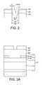
- FIG. 2illustrates a manufacturing process of etching the silicon-containing material layer according to the thin layer according to an embodiment of the present disclosure
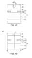
- providing the underlying layer 110includes, such as, forming a diffusion barrier 111 , forming a dielectric layer 112 on the diffusion barrier 111 , forming a SiON layer 113 on the dielectric layer 112 , forming a patterned layer 114 on the SiON layer 113 , and forming a cap oxide 115 layer on the patterned layer 114 .
- the diffusion barrier 111may be an etching stop layer as well, and the material of the diffusion barrier 111 may comprise nitrogen-doped silicon carbide (NDC).
- the dielectric layer 112may comprise an ultra-low-k (ULK) material.
- the patterned layer 114may be a patterned hard mask, including a TiN layer 114 a and a Ti layer 114 b.
- the manufacturing process of forming the tri-layered photoresistincludes such as the following steps.
- the bottom photoresist layer 120is formed on the underlying layer 110
- the silicon-containing material layer 130is formed on the bottom photoresist layer 120
- the patterned photoresist layer 140is formed on the silicon-containing material layer 130 .
- an etching processis performed for forming a via hole, and the etching process includes etching the silicon-containing material layer 130 according to the thin layer 150 on the tri-layered photoresist. As shown in FIG. 1C , the etched silicon-containing material layer 130 ′ forms a via hole V 1 extending to the top surface of the bottom photoresist layer 120 . Due to the reduced critical dimension in the patterned photoresist layer 140 by the thickness T 1 of the thin layer 150 , the critical dimension D 2 of the via hole V 1 is reduced as well.
- a conductive materialmay be further filled into the via hole V 2 for forming a via contact (not shown in figures).
- FIG. 2a manufacturing process of etching the silicon-containing material layer according to the thin layer according to an embodiment of the present disclosure is illustrated.
- the first critical dimension D 1 of the first through hole 140 a of the patterned photoresist layer 140is shown.
- the thickness T 1 of the thin layer 150is adjustable and determined according to the first critical dimension D 1 and an etching bias from the etching process.
- the etching biasis defined as the difference in critical dimensions in the silicon-containing material layer before and after performing the etching process.
- the thickness T 1 of the thin layer 150is adjustable and determined according to the first critical dimension D 1 of the first through hole 140 a and the etching bias.
- the thickness T 1 of the thin layer 150may be controlled by an advanced process control (APC) system according to the first critical dimension D 1 of the first through hole 140 a and the etching bias from the etching process.
- APIadvanced process control
- the etched silicon-containing material layer 130 ′forms a tapered-shaped via hole V 1
- the etching bias Bis defined as the difference between the critical dimension D 2 ′ before the etching process and the critical dimension D 2 after the etching process in the silicon-containing material layer 130 ′.
- the first critical dimension D 1 of the first through hole 140 ais 72 nm
- the critical dimension D 2 of the via hole V 1is predetermined to be 42 nm
- the etching bias Bis 20 nm
- the first critical dimension D 1 of the first through hole 140 ais 70 nm
- the critical dimension D 2 of the via hole V 1is predetermined to be 42 nm
- the etching bias Bis 20 nm
- the thickness T 1 of the thin layer 150 determined according to the above-mentioned advanced process control systemcan provide the via holes V 1 with uniform sizes, regardless of the variation of the critical dimensions D 1 .
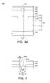
- a multi-layered photoresistis formed on the underlying layer 110 .
- the manufacturing process of forming the multi-layered photoresistincludes such as the following steps: forming a hard mask layer on the underlying layer 110 and forming the patterned photoresist layer 140 on the hard mask layer.
- the patterned photoresist layer 140has a first through hole 140 a.
- the hard mask layercomprises at least one of a silicon-containing material layer, a bottom anti-reflective coating (BARC), or a bottom photoresist layer 120 .
- the hard mask layeris a silicon-containing material layer 230 .
- a first etching processis performed for forming a patterned hard mask layer 230 ′.
- forming the patterned hard mask layer 230 ′is by such as etching the hard mask layer (silicon-containing material layer 230 ) according to the patterned photoresist layer 140 , and a second through hole 230 a is formed within the patterned hard mask layer 230 ′.
- an atomic layer deposition processis performed for forming a thin layer 150 on the patterned hard mask layer 230 ′.
- the ALD processis performed to the patterned photoresist 140 and the patterned hard mask layer 230 ′ for forming the thin layer 150 on the patterned photoresist 140 and in the second through hole 230 a of the patterned hard mask layer 230 ′.
- the thickness T 1 of the thin layer 150 on the top surface of the patterned photoresist 140 as well as on the sidewalls of the second through hole 230 ais uniform.
- the ALD processmay be performed to the patterned hard mask layer for forming the thin layer 150 on the patterned hard mask layer and in the second through hole of the patterned hard mask layer (not shown in figures).
- a conductive materialmay be further filled into the via hole V 3 for forming a via contact (not shown).
- the thickness T 1 of the thin layer 150is adjustable and determined according to the first critical dimension D 1 of the patterned photoresist layer 140 and a first etching bias from the first etching process.
- the first etching biasis defined as the difference in critical dimensions in the patterned hard mask layer 230 ′ before and after performing the first etching process.
- the thickness T 1 of the thin layer 150is adjustable and determined according to the first critical dimension D 1 of the first through hole 140 a and the first etching bias.
- the thickness T 1 of the thin layer 150may be controlled by an advanced process control system according to the first critical dimension D 1 of the first through hole 140 a and the first etching bias.
- the second critical dimensionmay be the critical dimension D 3 as shown in FIG. 4 .
- the critical dimension D 3is not predetermined to be as a fixed value in the present embodiment; on the contrary, the second critical dimension of the second through hole 230 a may vary depending on the manufacturing process thereof. Referring to FIGS. 3D and 4 , with the critical dimension D 4 of the via hole V 3 predetermined at a fixed value, the thickness T 1 of the thin layer 150 is adjusted and determined according to the second critical dimension (critical dimension D 3 ), the second etching bias from the second etching process performed to the underlying layer 110 , and the predetermined value of the critical dimension D 4 of the via hole V 3 .
- the thickness T 1 of the thin layer 150may be further determined according to the predetermined critical dimension D 4 of the via hole V 3 , the initial critical dimension D 1 within the patterned photoresist layer 140 , and the two etching biases from the two etching processes.
- the thickness T 1 of the thin layer 150 determined according to the above-mentioned advanced process control systemcan provide the via holes V 1 and/or V 3 with uniform sizes, regardless of the variation of the critical dimensions of the through holes 140 a and/or 230 a.
Landscapes
- Engineering & Computer Science (AREA)
- Physics & Mathematics (AREA)
- Condensed Matter Physics & Semiconductors (AREA)
- General Physics & Mathematics (AREA)
- Manufacturing & Machinery (AREA)
- Computer Hardware Design (AREA)
- Microelectronics & Electronic Packaging (AREA)
- Power Engineering (AREA)
- Chemical & Material Sciences (AREA)
- Inorganic Chemistry (AREA)
- Internal Circuitry In Semiconductor Integrated Circuit Devices (AREA)
Abstract
Description
Claims (20)
Priority Applications (1)
| Application Number | Priority Date | Filing Date | Title |
|---|---|---|---|
| US14/020,948US8883648B1 (en) | 2013-09-09 | 2013-09-09 | Manufacturing method of semiconductor structure |
Applications Claiming Priority (1)
| Application Number | Priority Date | Filing Date | Title |
|---|---|---|---|
| US14/020,948US8883648B1 (en) | 2013-09-09 | 2013-09-09 | Manufacturing method of semiconductor structure |
Publications (1)
| Publication Number | Publication Date |
|---|---|
| US8883648B1true US8883648B1 (en) | 2014-11-11 |
Family
ID=51845736
Family Applications (1)
| Application Number | Title | Priority Date | Filing Date |
|---|---|---|---|
| US14/020,948ActiveUS8883648B1 (en) | 2013-09-09 | 2013-09-09 | Manufacturing method of semiconductor structure |
Country Status (1)
| Country | Link |
|---|---|
| US (1) | US8883648B1 (en) |
Cited By (15)
| Publication number | Priority date | Publication date | Assignee | Title |
|---|---|---|---|---|
| US20150087150A1 (en)* | 2013-09-24 | 2015-03-26 | Semiconductor Manufacturing International (Beijing) Corporation | Semiconductor structures and fabrication method thereof |
| US20150221549A1 (en)* | 2014-02-06 | 2015-08-06 | International Business Machines Corporation | Process methods for advanced interconnect patterning |
| US9397007B2 (en)* | 2013-01-06 | 2016-07-19 | Institute of Microelectronics, Chinese Academy of Sciences | Method for manufacturing semiconductor structure through forming an additional layer inside opening of a photoresist layer |
| US9536964B2 (en)* | 2015-05-29 | 2017-01-03 | Taiwan Semiconductor Manufacturing Company, Ltd. | Method for forming via profile of interconnect structure of semiconductor device structure |
| US9543203B1 (en) | 2015-07-02 | 2017-01-10 | United Microelectronics Corp. | Method of fabricating a semiconductor structure with a self-aligned contact |
| US9679850B2 (en)* | 2015-10-30 | 2017-06-13 | Taiwan Semiconductor Manufacturing Company Ltd. | Method of fabricating semiconductor structure |
| US20180323078A1 (en)* | 2015-12-24 | 2018-11-08 | Intel Corporation | Pitch division using directed self-assembly |
| CN109326554A (en)* | 2017-07-31 | 2019-02-12 | 台湾积体电路制造股份有限公司 | Semiconductor structure and method of forming the same |
| US10276378B1 (en)* | 2017-10-30 | 2019-04-30 | Taiwan Semiconductor Manufacturing Co., Ltd. | Method of forming funnel-like opening for semiconductor device structure |
| US10468407B2 (en) | 2015-05-15 | 2019-11-05 | Taiwan Semiconductor Manufacturing Co., Ltd. | Fin field effect transistor (FinFET) device structure with uneven gate structure |
| US20200035505A1 (en)* | 2018-07-27 | 2020-01-30 | Applied Materials, Inc. | 3D NAND Etch |
| US20200357634A1 (en)* | 2017-09-29 | 2020-11-12 | Taiwan Semiconductor Manufacturing Co., Ltd. | Method for Manufacturing a Semiconductor Device |
| US11398377B2 (en)* | 2020-01-14 | 2022-07-26 | International Business Machines Corporation | Bilayer hardmask for direct print lithography |
| WO2024144886A1 (en)* | 2022-12-28 | 2024-07-04 | Tokyo Electron Limited | Methods for forming semiconductor devices using modified photomask layer |
| US12444687B2 (en) | 2022-02-14 | 2025-10-14 | Taiwan Semiconductor Manufacturing Company, Ltd. | Interconnect structure with vias extending through multiple dielectric layers |
Citations (31)
| Publication number | Priority date | Publication date | Assignee | Title |
|---|---|---|---|---|
| US4256514A (en)* | 1978-11-03 | 1981-03-17 | International Business Machines Corporation | Method for forming a narrow dimensioned region on a body |
| US4325182A (en)* | 1980-08-25 | 1982-04-20 | General Electric Company | Fast isolation diffusion |
| US4801350A (en)* | 1986-12-29 | 1989-01-31 | Motorola, Inc. | Method for obtaining submicron features from optical lithography technology |
| US4830975A (en)* | 1983-01-13 | 1989-05-16 | National Semiconductor Corporation | Method of manufacture a primos device |
| US4838991A (en)* | 1987-10-30 | 1989-06-13 | International Business Machines Corporation | Process for defining organic sidewall structures |
| US4871630A (en)* | 1986-10-28 | 1989-10-03 | International Business Machines Corporation | Mask using lithographic image size reduction |
| US5296410A (en)* | 1992-12-16 | 1994-03-22 | Samsung Electronics Co., Ltd. | Method for separating fine patterns of a semiconductor device |
| US5411824A (en)* | 1993-01-21 | 1995-05-02 | Sematech, Inc. | Phase shifting mask structure with absorbing/attenuating sidewalls for improved imaging |
| US5418095A (en)* | 1993-01-21 | 1995-05-23 | Sematech, Inc. | Method of fabricating phase shifters with absorbing/attenuating sidewalls using an additive process |
| US5710066A (en)* | 1994-06-01 | 1998-01-20 | Mitsubishi Denki Kabushiki Kaisha | Method of forming fine patterns |
| US5882535A (en)* | 1997-02-04 | 1999-03-16 | Micron Technology, Inc. | Method for forming a hole in a semiconductor device |
| US5895740A (en)* | 1996-11-13 | 1999-04-20 | Vanguard International Semiconductor Corp. | Method of forming contact holes of reduced dimensions by using in-situ formed polymeric sidewall spacers |
| US6261962B1 (en)* | 1996-08-01 | 2001-07-17 | Surface Technology Systems Limited | Method of surface treatment of semiconductor substrates |
| US6368974B1 (en)* | 1999-08-02 | 2002-04-09 | United Microelectronics Corp. | Shrinking equal effect critical dimension of mask by in situ polymer deposition and etching |
| US6750150B2 (en) | 2001-10-18 | 2004-06-15 | Macronix International Co., Ltd. | Method for reducing dimensions between patterns on a photoresist |
| US6770209B2 (en)* | 2002-01-09 | 2004-08-03 | International Business Machines Corporation | Isotropic deposition for trench narrowing of features to be created by reactive ion etch processing |
| US6864184B1 (en)* | 2004-02-05 | 2005-03-08 | Advanced Micro Devices, Inc. | Method for reducing critical dimension attainable via the use of an organic conforming layer |
| US6877213B2 (en)* | 2002-01-07 | 2005-04-12 | International Business Machines Corporation | Feature size reduction in thin film magnetic head using low temperature deposition coating of photolithographically-defined trenches |
| US7250371B2 (en)* | 2003-08-26 | 2007-07-31 | Lam Research Corporation | Reduction of feature critical dimensions |
| US20070284690A1 (en)* | 2005-08-18 | 2007-12-13 | Lam Research Corporation | Etch features with reduced line edge roughness |
| US7449230B2 (en) | 2002-03-05 | 2008-11-11 | Brewer Science Inc. | Lithography pattern shrink process and articles |
| US20090130850A1 (en)* | 2007-11-16 | 2009-05-21 | Kang Hyun Lee | Semiconductor Devices and Method of Fabricating the Same |
| US20090191711A1 (en)* | 2008-01-30 | 2009-07-30 | Ying Rui | Hardmask open process with enhanced cd space shrink and reduction |
| US7695632B2 (en)* | 2005-05-31 | 2010-04-13 | Lam Research Corporation | Critical dimension reduction and roughness control |
| US7772122B2 (en)* | 2008-09-18 | 2010-08-10 | Lam Research Corporation | Sidewall forming processes |
| US8053897B2 (en)* | 2005-03-10 | 2011-11-08 | X-Fab Semiconductor Foundries Ag | Production of a carrier wafer contact in trench insulated integrated SOI circuits having high-voltage components |
| US8172948B2 (en)* | 2006-10-10 | 2012-05-08 | Lam Research Corporation | De-fluoridation process |
| US20120244710A1 (en)* | 2011-03-23 | 2012-09-27 | Globalfoundries Dresden Module One Limited Liability Company & Co. Kg | Shrinkage of Critical Dimensions in a Semiconductor Device by Selective Growth of a Mask Material |
| US8377820B2 (en)* | 2009-01-30 | 2013-02-19 | Globalfoundries Inc. | Method of forming a metallization system of a semiconductor device by using a hard mask for defining the via size |
| US8501395B2 (en)* | 2007-06-04 | 2013-08-06 | Applied Materials, Inc. | Line edge roughness reduction and double patterning |
| US8741552B2 (en)* | 2009-02-11 | 2014-06-03 | Taiwan Semiconductor Manufacturing Company, Ltd. | Double patterning strategy for contact hole and trench in photolithography |
- 2013
- 2013-09-09USUS14/020,948patent/US8883648B1/enactiveActive
Patent Citations (35)
| Publication number | Priority date | Publication date | Assignee | Title |
|---|---|---|---|---|
| US4256514A (en)* | 1978-11-03 | 1981-03-17 | International Business Machines Corporation | Method for forming a narrow dimensioned region on a body |
| US4325182A (en)* | 1980-08-25 | 1982-04-20 | General Electric Company | Fast isolation diffusion |
| US4830975A (en)* | 1983-01-13 | 1989-05-16 | National Semiconductor Corporation | Method of manufacture a primos device |
| US4871630A (en)* | 1986-10-28 | 1989-10-03 | International Business Machines Corporation | Mask using lithographic image size reduction |
| US4801350A (en)* | 1986-12-29 | 1989-01-31 | Motorola, Inc. | Method for obtaining submicron features from optical lithography technology |
| US4838991A (en)* | 1987-10-30 | 1989-06-13 | International Business Machines Corporation | Process for defining organic sidewall structures |
| US5296410A (en)* | 1992-12-16 | 1994-03-22 | Samsung Electronics Co., Ltd. | Method for separating fine patterns of a semiconductor device |
| US5411824A (en)* | 1993-01-21 | 1995-05-02 | Sematech, Inc. | Phase shifting mask structure with absorbing/attenuating sidewalls for improved imaging |
| US5418095A (en)* | 1993-01-21 | 1995-05-23 | Sematech, Inc. | Method of fabricating phase shifters with absorbing/attenuating sidewalls using an additive process |
| US5710066A (en)* | 1994-06-01 | 1998-01-20 | Mitsubishi Denki Kabushiki Kaisha | Method of forming fine patterns |
| US6261962B1 (en)* | 1996-08-01 | 2001-07-17 | Surface Technology Systems Limited | Method of surface treatment of semiconductor substrates |
| US5895740A (en)* | 1996-11-13 | 1999-04-20 | Vanguard International Semiconductor Corp. | Method of forming contact holes of reduced dimensions by using in-situ formed polymeric sidewall spacers |
| US5882535A (en)* | 1997-02-04 | 1999-03-16 | Micron Technology, Inc. | Method for forming a hole in a semiconductor device |
| US6368974B1 (en)* | 1999-08-02 | 2002-04-09 | United Microelectronics Corp. | Shrinking equal effect critical dimension of mask by in situ polymer deposition and etching |
| US6750150B2 (en) | 2001-10-18 | 2004-06-15 | Macronix International Co., Ltd. | Method for reducing dimensions between patterns on a photoresist |
| US7033948B2 (en)* | 2001-10-18 | 2006-04-25 | Macronix International Co., Ltd. | Method for reducing dimensions between patterns on a photoresist |
| US6877213B2 (en)* | 2002-01-07 | 2005-04-12 | International Business Machines Corporation | Feature size reduction in thin film magnetic head using low temperature deposition coating of photolithographically-defined trenches |
| US6770209B2 (en)* | 2002-01-09 | 2004-08-03 | International Business Machines Corporation | Isotropic deposition for trench narrowing of features to be created by reactive ion etch processing |
| US7449230B2 (en) | 2002-03-05 | 2008-11-11 | Brewer Science Inc. | Lithography pattern shrink process and articles |
| US7250371B2 (en)* | 2003-08-26 | 2007-07-31 | Lam Research Corporation | Reduction of feature critical dimensions |
| US7541291B2 (en)* | 2003-08-26 | 2009-06-02 | Lam Research Corporation | Reduction of feature critical dimensions |
| US6864184B1 (en)* | 2004-02-05 | 2005-03-08 | Advanced Micro Devices, Inc. | Method for reducing critical dimension attainable via the use of an organic conforming layer |
| US8053897B2 (en)* | 2005-03-10 | 2011-11-08 | X-Fab Semiconductor Foundries Ag | Production of a carrier wafer contact in trench insulated integrated SOI circuits having high-voltage components |
| US8614149B2 (en)* | 2005-05-31 | 2013-12-24 | Lam Research Corporation | Critical dimension reduction and roughness control |
| US7695632B2 (en)* | 2005-05-31 | 2010-04-13 | Lam Research Corporation | Critical dimension reduction and roughness control |
| US8268118B2 (en)* | 2005-05-31 | 2012-09-18 | Lam Research Corporation | Critical dimension reduction and roughness control |
| US20070284690A1 (en)* | 2005-08-18 | 2007-12-13 | Lam Research Corporation | Etch features with reduced line edge roughness |
| US8172948B2 (en)* | 2006-10-10 | 2012-05-08 | Lam Research Corporation | De-fluoridation process |
| US8501395B2 (en)* | 2007-06-04 | 2013-08-06 | Applied Materials, Inc. | Line edge roughness reduction and double patterning |
| US20090130850A1 (en)* | 2007-11-16 | 2009-05-21 | Kang Hyun Lee | Semiconductor Devices and Method of Fabricating the Same |
| US20090191711A1 (en)* | 2008-01-30 | 2009-07-30 | Ying Rui | Hardmask open process with enhanced cd space shrink and reduction |
| US7772122B2 (en)* | 2008-09-18 | 2010-08-10 | Lam Research Corporation | Sidewall forming processes |
| US8377820B2 (en)* | 2009-01-30 | 2013-02-19 | Globalfoundries Inc. | Method of forming a metallization system of a semiconductor device by using a hard mask for defining the via size |
| US8741552B2 (en)* | 2009-02-11 | 2014-06-03 | Taiwan Semiconductor Manufacturing Company, Ltd. | Double patterning strategy for contact hole and trench in photolithography |
| US20120244710A1 (en)* | 2011-03-23 | 2012-09-27 | Globalfoundries Dresden Module One Limited Liability Company & Co. Kg | Shrinkage of Critical Dimensions in a Semiconductor Device by Selective Growth of a Mask Material |
Cited By (27)
| Publication number | Priority date | Publication date | Assignee | Title |
|---|---|---|---|---|
| US9397007B2 (en)* | 2013-01-06 | 2016-07-19 | Institute of Microelectronics, Chinese Academy of Sciences | Method for manufacturing semiconductor structure through forming an additional layer inside opening of a photoresist layer |
| US20150087150A1 (en)* | 2013-09-24 | 2015-03-26 | Semiconductor Manufacturing International (Beijing) Corporation | Semiconductor structures and fabrication method thereof |
| US9111874B2 (en)* | 2013-09-24 | 2015-08-18 | Semiconductor Manufacturing International (Beijing) Corporation | Semiconductor structures and fabrication method thereof |
| US9202749B2 (en)* | 2014-02-06 | 2015-12-01 | International Business Machines Corporation | Process methods for advanced interconnect patterning |
| US20150221549A1 (en)* | 2014-02-06 | 2015-08-06 | International Business Machines Corporation | Process methods for advanced interconnect patterning |
| US10468407B2 (en) | 2015-05-15 | 2019-11-05 | Taiwan Semiconductor Manufacturing Co., Ltd. | Fin field effect transistor (FinFET) device structure with uneven gate structure |
| US11139295B2 (en) | 2015-05-22 | 2021-10-05 | Taiwan Semiconductor Manufacturing Co., Ltd. | Fin field effect transistor (FinFET) device and method |
| US9997401B2 (en) | 2015-05-29 | 2018-06-12 | Taiwan Semiconductor Manufacturing Company, Ltd. | Method for forming a via profile of interconnect structure of semiconductor device structure |
| US9536964B2 (en)* | 2015-05-29 | 2017-01-03 | Taiwan Semiconductor Manufacturing Company, Ltd. | Method for forming via profile of interconnect structure of semiconductor device structure |
| TWI602224B (en)* | 2015-05-29 | 2017-10-11 | 台灣積體電路製造股份有限公司 | Method of forming semiconductor device structure |
| US9543203B1 (en) | 2015-07-02 | 2017-01-10 | United Microelectronics Corp. | Method of fabricating a semiconductor structure with a self-aligned contact |
| US9679850B2 (en)* | 2015-10-30 | 2017-06-13 | Taiwan Semiconductor Manufacturing Company Ltd. | Method of fabricating semiconductor structure |
| US20190287914A1 (en)* | 2015-10-30 | 2019-09-19 | Taiwan Semiconductor Manufacturing Company Ltd. | Semiconductor structure |
| US10867921B2 (en)* | 2015-10-30 | 2020-12-15 | Taiwan Semiconductor Manufacturing Company Ltd. | Semiconductor structure with tapered conductor |
| US20180323078A1 (en)* | 2015-12-24 | 2018-11-08 | Intel Corporation | Pitch division using directed self-assembly |
| CN109326554A (en)* | 2017-07-31 | 2019-02-12 | 台湾积体电路制造股份有限公司 | Semiconductor structure and method of forming the same |
| US11251127B2 (en) | 2017-07-31 | 2022-02-15 | Taiwan Semiconductor Manufacturing Company, Ltd. | Interconnect structure with vias extending through multiple dielectric layers |
| US20200357634A1 (en)* | 2017-09-29 | 2020-11-12 | Taiwan Semiconductor Manufacturing Co., Ltd. | Method for Manufacturing a Semiconductor Device |
| US10276378B1 (en)* | 2017-10-30 | 2019-04-30 | Taiwan Semiconductor Manufacturing Co., Ltd. | Method of forming funnel-like opening for semiconductor device structure |
| US10886140B2 (en)* | 2018-07-27 | 2021-01-05 | Applied Materials, Inc. | 3D NAND etch |
| US20200035505A1 (en)* | 2018-07-27 | 2020-01-30 | Applied Materials, Inc. | 3D NAND Etch |
| US11515170B2 (en) | 2018-07-27 | 2022-11-29 | Applied Materials, Inc. | 3D NAND etch |
| US11398377B2 (en)* | 2020-01-14 | 2022-07-26 | International Business Machines Corporation | Bilayer hardmask for direct print lithography |
| US12444687B2 (en) | 2022-02-14 | 2025-10-14 | Taiwan Semiconductor Manufacturing Company, Ltd. | Interconnect structure with vias extending through multiple dielectric layers |
| WO2024144886A1 (en)* | 2022-12-28 | 2024-07-04 | Tokyo Electron Limited | Methods for forming semiconductor devices using modified photomask layer |
| US20240222118A1 (en)* | 2022-12-28 | 2024-07-04 | Tokyo Electron Limited | Methods for forming semiconductor devices using modified photomask layer |
| US12424442B2 (en)* | 2022-12-28 | 2025-09-23 | Tokyo Electron Limited | Methods for forming semiconductor devices using modified photomask layer |
Similar Documents
| Publication | Publication Date | Title |
|---|---|---|
| US8883648B1 (en) | Manufacturing method of semiconductor structure | |
| US10079145B2 (en) | Method for pattern formation on a substrate, associated semiconductor devices, and uses of the method | |
| US9991156B2 (en) | Self-aligned quadruple patterning (SAQP) for routing layouts including multi-track jogs | |
| US8916337B2 (en) | Dual hard mask lithography process | |
| KR102250656B1 (en) | Method of forming patterns for semiconductor device | |
| US8138093B2 (en) | Method for forming trenches having different widths and the same depth | |
| US8586478B2 (en) | Method of making a semiconductor device | |
| US8728945B2 (en) | Method for patterning sublithographic features | |
| US9679809B1 (en) | Method of forming self aligned continuity blocks for mandrel and non-mandrel interconnect lines | |
| CN104425567B (en) | The system and method for improving passivation integrity | |
| US9581900B2 (en) | Self aligned patterning with multiple resist layers | |
| TWI660424B (en) | Method of forming ana regions in an integrated circuit | |
| US8377795B2 (en) | Cut first methodology for double exposure double etch integration | |
| JP5100198B2 (en) | Method for forming fine pattern of semiconductor element | |
| US9412612B2 (en) | Method of forming semiconductor device | |
| CN109494149B (en) | Method for manufacturing semiconductor structure | |
| KR100875653B1 (en) | Method of forming fine pattern of semiconductor device | |
| US9275960B2 (en) | Integrated circuit formed using spacer-like copper deposition | |
| US20150241785A1 (en) | Method of manufacturing semiconductor device | |
| KR20110138201A (en) | Method for manufacturing a semiconductor device | |
| KR20090000882A (en) | Method of forming fine pattern of semiconductor device | |
| KR20070063319A (en) | Method for Forming Fine Line Pattern of Semiconductor Device | |
| KR100694975B1 (en) | Metal wiring formation method of semiconductor device | |
| KR20100008173A (en) | Method for fabricating semiconductor device | |
| KR20080002534A (en) | Method of forming fine pattern of semiconductor device |
Legal Events
| Date | Code | Title | Description |
|---|---|---|---|
| AS | Assignment | Owner name:UNITED MICROELECTRONICS CORP., TAIWAN Free format text:ASSIGNMENT OF ASSIGNORS INTEREST;ASSIGNORS:HSIEH, MING-DA;LAI, YU-TSUNG;CHEN, HSUAN-HSU;REEL/FRAME:031161/0559 Effective date:20130901 | |
| FEPP | Fee payment procedure | Free format text:PAYOR NUMBER ASSIGNED (ORIGINAL EVENT CODE: ASPN); ENTITY STATUS OF PATENT OWNER: LARGE ENTITY | |
| STCF | Information on status: patent grant | Free format text:PATENTED CASE | |
| MAFP | Maintenance fee payment | Free format text:PAYMENT OF MAINTENANCE FEE, 4TH YEAR, LARGE ENTITY (ORIGINAL EVENT CODE: M1551) Year of fee payment:4 | |
| AS | Assignment | Owner name:MARLIN SEMICONDUCTOR LIMITED, IRELAND Free format text:ASSIGNMENT OF ASSIGNORS INTEREST;ASSIGNOR:UNITED MICROELECTRONICS CORPORATION;REEL/FRAME:056991/0292 Effective date:20210618 | |
| MAFP | Maintenance fee payment | Free format text:PAYMENT OF MAINTENANCE FEE, 8TH YEAR, LARGE ENTITY (ORIGINAL EVENT CODE: M1552); ENTITY STATUS OF PATENT OWNER: LARGE ENTITY Year of fee payment:8 |