US8883600B1 - Transistor having reduced junction leakage and methods of forming thereof - Google Patents
Transistor having reduced junction leakage and methods of forming thereofDownload PDFInfo
- Publication number
- US8883600B1 US8883600B1US13/725,152US201213725152AUS8883600B1US 8883600 B1US8883600 B1US 8883600B1US 201213725152 AUS201213725152 AUS 201213725152AUS 8883600 B1US8883600 B1US 8883600B1
- Authority
- US
- United States
- Prior art keywords
- layer
- spacer
- transistor
- region
- thickness
- Prior art date
- Legal status (The legal status is an assumption and is not a legal conclusion. Google has not performed a legal analysis and makes no representation as to the accuracy of the status listed.)
- Active, expires
Links
Images


Classifications
- H—ELECTRICITY
- H10—SEMICONDUCTOR DEVICES; ELECTRIC SOLID-STATE DEVICES NOT OTHERWISE PROVIDED FOR
- H10D—INORGANIC ELECTRIC SEMICONDUCTOR DEVICES
- H10D30/00—Field-effect transistors [FET]
- H10D30/60—Insulated-gate field-effect transistors [IGFET]
- H10D30/601—Insulated-gate field-effect transistors [IGFET] having lightly-doped drain or source extensions, e.g. LDD IGFETs or DDD IGFETs
- H01L29/7833—
- H01L29/6656—
- H—ELECTRICITY
- H10—SEMICONDUCTOR DEVICES; ELECTRIC SOLID-STATE DEVICES NOT OTHERWISE PROVIDED FOR
- H10D—INORGANIC ELECTRIC SEMICONDUCTOR DEVICES
- H10D30/00—Field-effect transistors [FET]
- H10D30/01—Manufacture or treatment
- H10D30/021—Manufacture or treatment of FETs having insulated gates [IGFET]
- H10D30/0223—Manufacture or treatment of FETs having insulated gates [IGFET] having source and drain regions or source and drain extensions self-aligned to sides of the gate
- H10D30/0227—Manufacture or treatment of FETs having insulated gates [IGFET] having source and drain regions or source and drain extensions self-aligned to sides of the gate having both lightly-doped source and drain extensions and source and drain regions self-aligned to the sides of the gate, e.g. lightly-doped drain [LDD] MOSFET or double-diffused drain [DDD] MOSFET
- H—ELECTRICITY
- H10—SEMICONDUCTOR DEVICES; ELECTRIC SOLID-STATE DEVICES NOT OTHERWISE PROVIDED FOR
- H10D—INORGANIC ELECTRIC SEMICONDUCTOR DEVICES
- H10D30/00—Field-effect transistors [FET]
- H10D30/60—Insulated-gate field-effect transistors [IGFET]
- H10D30/601—Insulated-gate field-effect transistors [IGFET] having lightly-doped drain or source extensions, e.g. LDD IGFETs or DDD IGFETs
- H10D30/605—Insulated-gate field-effect transistors [IGFET] having lightly-doped drain or source extensions, e.g. LDD IGFETs or DDD IGFETs having significant overlap between the lightly-doped extensions and the gate electrode
- H—ELECTRICITY
- H10—SEMICONDUCTOR DEVICES; ELECTRIC SOLID-STATE DEVICES NOT OTHERWISE PROVIDED FOR
- H10D—INORGANIC ELECTRIC SEMICONDUCTOR DEVICES
- H10D62/00—Semiconductor bodies, or regions thereof, of devices having potential barriers
- H10D62/10—Shapes, relative sizes or dispositions of the regions of the semiconductor bodies; Shapes of the semiconductor bodies
- H10D62/13—Semiconductor regions connected to electrodes carrying current to be rectified, amplified or switched, e.g. source or drain regions
- H10D62/149—Source or drain regions of field-effect devices
- H10D62/151—Source or drain regions of field-effect devices of IGFETs
- H—ELECTRICITY
- H10—SEMICONDUCTOR DEVICES; ELECTRIC SOLID-STATE DEVICES NOT OTHERWISE PROVIDED FOR
- H10D—INORGANIC ELECTRIC SEMICONDUCTOR DEVICES
- H10D62/00—Semiconductor bodies, or regions thereof, of devices having potential barriers
- H10D62/10—Shapes, relative sizes or dispositions of the regions of the semiconductor bodies; Shapes of the semiconductor bodies
- H10D62/17—Semiconductor regions connected to electrodes not carrying current to be rectified, amplified or switched, e.g. channel regions
- H10D62/213—Channel regions of field-effect devices
- H10D62/221—Channel regions of field-effect devices of FETs
- H10D62/235—Channel regions of field-effect devices of FETs of IGFETs
- H10D62/299—Channel regions of field-effect devices of FETs of IGFETs having lateral doping variations
- H—ELECTRICITY
- H10—SEMICONDUCTOR DEVICES; ELECTRIC SOLID-STATE DEVICES NOT OTHERWISE PROVIDED FOR
- H10D—INORGANIC ELECTRIC SEMICONDUCTOR DEVICES
- H10D62/00—Semiconductor bodies, or regions thereof, of devices having potential barriers
- H10D62/10—Shapes, relative sizes or dispositions of the regions of the semiconductor bodies; Shapes of the semiconductor bodies
- H10D62/17—Semiconductor regions connected to electrodes not carrying current to be rectified, amplified or switched, e.g. channel regions
- H10D62/213—Channel regions of field-effect devices
- H10D62/221—Channel regions of field-effect devices of FETs
- H10D62/235—Channel regions of field-effect devices of FETs of IGFETs
- H10D62/314—Channel regions of field-effect devices of FETs of IGFETs having vertical doping variations
- H—ELECTRICITY
- H10—SEMICONDUCTOR DEVICES; ELECTRIC SOLID-STATE DEVICES NOT OTHERWISE PROVIDED FOR
- H10D—INORGANIC ELECTRIC SEMICONDUCTOR DEVICES
- H10D62/00—Semiconductor bodies, or regions thereof, of devices having potential barriers
- H10D62/10—Shapes, relative sizes or dispositions of the regions of the semiconductor bodies; Shapes of the semiconductor bodies
- H10D62/17—Semiconductor regions connected to electrodes not carrying current to be rectified, amplified or switched, e.g. channel regions
- H10D62/351—Substrate regions of field-effect devices
- H10D62/357—Substrate regions of field-effect devices of FETs
- H10D62/364—Substrate regions of field-effect devices of FETs of IGFETs
- H10D62/371—Inactive supplementary semiconductor regions, e.g. for preventing punch-through, improving capacity effect or leakage current
- H—ELECTRICITY
- H10—SEMICONDUCTOR DEVICES; ELECTRIC SOLID-STATE DEVICES NOT OTHERWISE PROVIDED FOR
- H10D—INORGANIC ELECTRIC SEMICONDUCTOR DEVICES
- H10D64/00—Electrodes of devices having potential barriers
- H10D64/01—Manufacture or treatment
- H10D64/021—Manufacture or treatment using multiple gate spacer layers, e.g. bilayered sidewall spacers
- H—ELECTRICITY
- H10—SEMICONDUCTOR DEVICES; ELECTRIC SOLID-STATE DEVICES NOT OTHERWISE PROVIDED FOR
- H10D—INORGANIC ELECTRIC SEMICONDUCTOR DEVICES
- H10D30/00—Field-effect transistors [FET]
- H10D30/60—Insulated-gate field-effect transistors [IGFET]
- H10D30/601—Insulated-gate field-effect transistors [IGFET] having lightly-doped drain or source extensions, e.g. LDD IGFETs or DDD IGFETs
- H10D30/608—Insulated-gate field-effect transistors [IGFET] having lightly-doped drain or source extensions, e.g. LDD IGFETs or DDD IGFETs having non-planar bodies, e.g. having recessed gate electrodes
- H—ELECTRICITY
- H10—SEMICONDUCTOR DEVICES; ELECTRIC SOLID-STATE DEVICES NOT OTHERWISE PROVIDED FOR
- H10D—INORGANIC ELECTRIC SEMICONDUCTOR DEVICES
- H10D62/00—Semiconductor bodies, or regions thereof, of devices having potential barriers
- H10D62/01—Manufacture or treatment
- H10D62/021—Forming source or drain recesses by etching e.g. recessing by etching and then refilling
- H—ELECTRICITY
- H10—SEMICONDUCTOR DEVICES; ELECTRIC SOLID-STATE DEVICES NOT OTHERWISE PROVIDED FOR
- H10D—INORGANIC ELECTRIC SEMICONDUCTOR DEVICES
- H10D84/00—Integrated devices formed in or on semiconductor substrates that comprise only semiconducting layers, e.g. on Si wafers or on GaAs-on-Si wafers
- H10D84/01—Manufacture or treatment
- H10D84/0123—Integrating together multiple components covered by H10D12/00 or H10D30/00, e.g. integrating multiple IGBTs
- H10D84/0126—Integrating together multiple components covered by H10D12/00 or H10D30/00, e.g. integrating multiple IGBTs the components including insulated gates, e.g. IGFETs
- H10D84/0165—Integrating together multiple components covered by H10D12/00 or H10D30/00, e.g. integrating multiple IGBTs the components including insulated gates, e.g. IGFETs the components including complementary IGFETs, e.g. CMOS devices
- H10D84/017—Manufacturing their source or drain regions, e.g. silicided source or drain regions
- H—ELECTRICITY
- H10—SEMICONDUCTOR DEVICES; ELECTRIC SOLID-STATE DEVICES NOT OTHERWISE PROVIDED FOR
- H10D—INORGANIC ELECTRIC SEMICONDUCTOR DEVICES
- H10D84/00—Integrated devices formed in or on semiconductor substrates that comprise only semiconducting layers, e.g. on Si wafers or on GaAs-on-Si wafers
- H10D84/01—Manufacture or treatment
- H10D84/0123—Integrating together multiple components covered by H10D12/00 or H10D30/00, e.g. integrating multiple IGBTs
- H10D84/0126—Integrating together multiple components covered by H10D12/00 or H10D30/00, e.g. integrating multiple IGBTs the components including insulated gates, e.g. IGFETs
- H10D84/0165—Integrating together multiple components covered by H10D12/00 or H10D30/00, e.g. integrating multiple IGBTs the components including insulated gates, e.g. IGFETs the components including complementary IGFETs, e.g. CMOS devices
- H10D84/0193—Integrating together multiple components covered by H10D12/00 or H10D30/00, e.g. integrating multiple IGBTs the components including insulated gates, e.g. IGFETs the components including complementary IGFETs, e.g. CMOS devices the components including FinFETs
- H—ELECTRICITY
- H10—SEMICONDUCTOR DEVICES; ELECTRIC SOLID-STATE DEVICES NOT OTHERWISE PROVIDED FOR
- H10D—INORGANIC ELECTRIC SEMICONDUCTOR DEVICES
- H10D84/00—Integrated devices formed in or on semiconductor substrates that comprise only semiconducting layers, e.g. on Si wafers or on GaAs-on-Si wafers
- H10D84/01—Manufacture or treatment
- H10D84/02—Manufacture or treatment characterised by using material-based technologies
- H10D84/03—Manufacture or treatment characterised by using material-based technologies using Group IV technology, e.g. silicon technology or silicon-carbide [SiC] technology
- H10D84/038—Manufacture or treatment characterised by using material-based technologies using Group IV technology, e.g. silicon technology or silicon-carbide [SiC] technology using silicon technology, e.g. SiGe
Definitions
- Wafers and die manufactured with CMOS compatible die and having high uniformity screen and epitaxial layersare described.
- Variationscan occur due to process differences resulting in line edge variation, to other unwanted patterning effects that change channel, gate, or spacer size, to effective work function variation due to composition or crystal formation differences in the gate; or at the atomic scale, to random dopant fluctuations in quantity and spatial positioning of individual dopants in or near the transistor channel.
- Transistor matching issuesgenerally increase in significance as transistors are decreased in size.
- transistor width and length mismatchtypically increases inversely proportional according to the square root of the transistor area.
- transistor attributessuch as off-state current or threshold voltage variation
- the matching variation in nanometer scale transistorscan be great enough to create an unacceptable die, or result in high device failure rates.
- FIG. 1illustrates a three dimensional cross section of two adjacent transistors
- FIG. 2illustrates an inherent uncertainty in implant placement of dopant atoms in the respective channels of each transistor
- FIG. 3illustrates dopant placement along the channel with representative graphs of dopant concentration and placement
- FIG. 4illustrates a transistor formed on a well incorporating a heavily doped screening layer that completely extends under a gate area
- FIG. 5illustrates an epitaxial transistor having a retrograde dopant profile
- FIG. 6illustrates a similarly sized transistor with an atomically uniform screening layer
- FIG. 7illustrates etch steps that thin portions of the epitaxial layer or, through well proximity effects, allow an increase or decrease in dopant layer concentration near isolation structures
- FIG. 8illustrates constant thickness epitaxial layers with respect to a screening layer and a shallow trench isolation (STI) formed post-well implant to limit secondary dopant scattering;
- STIshallow trench isolation
- FIGS. 9A-9Dillustrate an example fabrication process for reducing junction leakage current in a transistor device
- FIG. 10illustrates a comparison of a structure without a dLDD region, a structure with a dLDD region having a first dose and a structure with a dLDD region 910 having a second dose;
- FIG. 11illustrates the effect on leakage current for various implant conditions of a dLDD region
- FIG. 12illustrates the effect that a dLDD region has on DIBL and ⁇ Vt
- FIG. 13illustrates a phosphorous grading implant for a transistor structure
- FIG. 14illustrates a comparison of a structure with different doses of Phosphorous
- FIG. 15illustrates a comparison of junction leakage current for different doses of Phosphorous
- FIG. 16illustrates a comparison of DIBL and ⁇ Vt at different doses and energies for Phosphorous
- FIG. 17illustrates a junction leakage current comparison of the dLDD approach and the Phosphorous grading approach to a reference that does not include these approaches;
- FIG. 18illustrates a comparison of DIBL and ⁇ Vt for each approach
- FIGS. 19A-19Cillustrate the steps for a distributed source/drain implant process
- FIG. 20illustrates a reduction in junction abruptness as a result of different thicknesses for a second offset spacer
- FIG. 21illustrates a comparison of threshold voltage and junction leakage for different thicknesses of a second offset spacer and different doses of Phosphorous
- FIG. 22illustrates a comparison of DIBL and ⁇ Vt for different thicknesses of a second offset spacer
- FIG. 23illustrates a deep implant for a compensation layer to help control out-diffusion from the source and drain.
- an ideally matched 14 nanometer node CMOS FET transistor pair 100 separated by shallow trench isolation 130includes two channels 110 and 112 formed from a semiconductor crystalline lattice (typically silicon or silicon-germanium).
- the channels 110 and 112incorporate a small number of positively or negatively electrically charged dopant atoms in the lattice such as boron or arsenic.
- dopantscan include deliberately implanted, but uncharged, diffusion mitigation atoms such as carbon, or various contaminant atoms that are either in the crystal lattice or in inter-lattice sites.
- each transistorwould have identical numbers and type of dopant atoms in the channel, and placement of the dopant atoms would be the same.
- the inherent uncertainty in implant placement of dopant atoms 120 and 122 in the respective channels of each transistorcan result, for example, in distinctly differing chains or clusters of dopants, or significant gaps in dopant placement, all of which lead to variations in transistor properties.
- an undoped epitaxial layer capable of acting as a channelcan be selectively grown, with controlled ion implantation to form a channel.
- an undoped epitaxial layer capable of acting as a channelcan be selectively grown, with controlled ion implantation to form a channel.
- substantially undoped channelsdo not eliminate all problems associated with dopant variation.
- FIG. 3which is a cartoon representing dopant placement along the channel, with representative graphs of dopant concentration and placement, variation in placement and amount of dopants around the channel will occur.
- halo implantsare often used to create a localized, graded dopant distribution near a transistor source and drain that extends into the channel. Halo implants are often required by transistor designers who want to reduce unwanted source/drain leakage conduction or “punch through” current.
- halo implantstend to introduce dopant species into unwanted areas through random dopant fluctuation caused by a variety of factors including scattering effects, crystal lattice channeling effects, lateral straggle, secondary diffusion, or simple variability in halo dopant energies and implantation angle.
- a transistor 200 formed on a wellcan incorporate a heavily doped, defined thickness, and highly doped screening layer 212 that completely extends in the lateral direction under a gate area.
- a gate induced electric field and consequent depletion zoneextends to the screening layer.
- an undoped blanket epitaxial layer grown on the wafer to form a layer that extends across multiple transistorsforms the undoped channel.
- a selective epitaxial channel layeris individually grown on this screening layer. In all instances, efforts are made to maintain the channel layer as undoped, unless the transistor design calls for a slightly doped channel, usually in order to achieve a higher threshold voltage.
- Unwanted diffusionis minimized by use of processing temperatures lower than 900 degrees or, or in addition to, Diffusion mitigation carbon caps can be included in the top layers of the screen to avoid the dopants from the screen from diffusing.
- Halo or threshold implantsare minimized or absent. Since there is minimal dopant presence in the channel, there is minimal variation in dopant positioning or concentration in the channel, and transistor channels are well matched. However, this does not completely eliminate the problem of transistor mismatch, since epitaxial layer thickness can vary under the gate, causing substantial differences in threshold voltage or other transistor performance characteristics.
- the screening layer 212is maintained as an atomically uniform layer that extends a precise distance 216 from a gate dielectric 208 .
- Screen layer 212extends laterally across the channel to abut the source and drain 219 , 220 .
- the screen layer 212is positioned to be either just underneath and abutting the bottom of or is located at approximately the bottom 1 ⁇ 3 to 1 ⁇ 4 of the lightly doped drain extensions 221 , 222 and extending downward to form a preselected thickness wherein the screen layer 212 approximately ends a distance above the bottom horizontal portion of the source and drain 219 , 220 .
- the targeted thickness for the screen layer 212depends on the device design in terms of requirements for threshold voltage and junction leakage, among other things, and to what extent a separate anti-punch through region (not shown) is used.
- the precise depth and thickness of the formed epitaxial channel layeris maintained over at least 80% of the gate dielectric area, and depth and thickness may slightly increase or decrease along the edge of the gate dielectric due to well proximity or etch effects.
- adjacent transistorswill have a gate dielectric to screening layer thickness that only varies within a one-half nanometer range, while more distant transistors on the same die will still have a channel layer thickness that varies within one nanometer.
- the screen layercan have a dopant concentration between 1 ⁇ 10 18 and 1 ⁇ 10 19 atoms per cubic centimeter or higher concentration, and further has a defined thickness of between five (5) and twenty (20) nanometers that varies no more than three (3) nanometers.
- the highly doped screen layertogether with the anti-punchthrough region (if present), creates a strong body coefficient, making the transistor amenable to be back-biased by electrically connecting a body tap to the screen layer.
- the back-biasing capability afforded by the highly doped screen layerenables greater flexibility for chip designs. Maintaining a controlled thickness 218 of the screening layer 212 additionally helps to match leakage current and body bias related performance factors.
- the tight control of screening layer positioningresults in tight control of the depletion zone when the transistor gate is activated. For comparison, as seen in two dimensional cross section embodied in FIG.
- a conventional transistor 300 having a retrograde dopant profile that is conventionally formed using buried implantsmay have an irregular depletion zone 304 due to varying concentrations and position of dopants.
- similarly sized transistor 302 with an atomically uniform screening layer 312will have a uniform depletion zone 314 set by the screening layer 312 , and with minimal edge effects.
- forming a blanket epitaxial layercan further include steps related to implanting or growing (via incorporation of dopants or diffusion mitigation atoms such as carbon) various channel dopant profiles deposited on a wafer over the screening layer. These profiles can extend across multiple die and transistor die blocks to give transistors with highly uniform three-dimensional structures. Such a blanket epitaxial layer, particularly after all well implants are done, helps to reduce upward migration of dopants emplaced during the well implants (to form the screening and other doped layers).
- lightly doped Vt adjustment layerscan be formed in but after formation of the epitaxial layer, allowing further adjustment of various transistor characteristics, including threshold voltage and leakage current, particularly in the context of forming a plurality of devices having different threshold voltage and other characteristics, for instance to create a SOC.
- DDC-FETsdeeply depleted channel field effect transistors
- DDC-FETshave a number of advantages in terms of electrical performance over conventional FETs at the same technology node. These advantages include, but are not in any way limited to, reduced subthreshold conduction (i.e., reduced off-state leakage current). Because modern integrated circuits typically include many millions of transistors, reduced off-state leakage current in these transistors can provide many benefits including a longer battery-life for a mobile device.
- DDC-FETsare also advantageous in terms of reduced threshold voltage variation across a given region of an integrated circuit. This type of threshold voltage variation is referred to as sigma Vt ( ⁇ Vt).
- One exemplary process for forming a transistorbegins at the well formation, which may be one of many different processes according to different embodiments and examples.
- Well formationis preferably before but may be after STI (shallow trench isolation) formation, depending on the application and results desired.
- Boron (B), indium (I) or other acceptor dopant materialsmay be used for P-type doping, and arsenic (As), antimony (Sb) or phosphorous (P) and other donor dopant of materials may be used for N-type doping.
- a germanium (Ge) followed by carbon (C) implant or in-situ doped carbon epi or cold or room temperature carbon implantmay optionally be performed to reduce dopant migration.
- Well implantsmay include sequential implant, and/or epitaxial growth and implant of punch through suppression regions, with screening layers having a defined thickness and higher dopant density than the punch through suppression region.
- Threshold voltage set layerscan be typically formed by implant or diffusion of dopants prior to or into a previously grown epitaxial layer formed on the already-doped screening region.
- the well formationmay include a beam line implant of Ge/C followed by or done after B (for N-FET), As (for P-FET), or Sb (for P-FET) in multiple steps so as to form distinct regions for screen and threshold voltage (and anti-punchthrough, if any) followed by an epitaxial (EPI) pre-clean process, and followed finally by non-selective blanket EPI deposition.
- the wellmay be formed using plasma implants of the same aforementioned materials, followed by an EPI pre-clean, then finally a non-selective (blanket) EPI deposition.
- well formationmay simply include well implants, followed by in-situ doped EPI (which may be selective or blanket) to form the screening layer and other doped regions.
- EPIwhich may be selective or blanket
- Embodiments described hereinallow for any one of a number of devices configured on a common substrate with different well structures and according to different parameters.
- Shallow trench isolation (STI) formationwhich, again, may occur before or after well formation, may include a low temperature trench sacrificial oxide (TSOX) liner at a temperature lower than 900 degrees C.
- TSOXtrench sacrificial oxide
- a gate stackmay be formed or otherwise constructed in a number of different ways, from different materials, and of different work functions.
- a gate-first processthat includes SiON/Metal/Poly and/or SiON/Poly, followed by high-k/Metal Gate.
- a gate-last processincludes a high-k/metal gate stack wherein the gate stack can either be formed with “high-k first-Metal gate last” flow or “high-k last-Metal gate last” flow.
- a metal gatethat includes a tunable range of work functions depending on the device construction.
- Source/Drain extensionslightly doped drain (LDD)
- LDDlightly doped drain
- the dimensions of the extensionscan be varied as required, and will depend in part on whether gate spacers are used and requirements for the gate width.
- the source and drain contactsare formed.
- the PMOS source and drainis created by way of selective epi.
- both PMOS and NMOS source and drainmay be formed by selective epi as performance enhancers for creating strained channels and/or reduction of contact resistance.
- etch stepscan thin portions of the epitaxial layer, or preferably, through well proximity effects, allow an increase or decrease in dopant layer concentration near isolation structures.
- Well proximity effectsare described in “Lateral Ion Implant Straggle and Mask Proximity Effect”, IEEE TRANSACTIONS ON ELECTRON DEVICES, VOL. 50, NO. 9, SEPTEMBER 2003.
- use of a screening layer covered by blanket epitaxial layerscan be used, along with post-well implant trench isolation eliminating much of the dopant scattering attributable to resist or isolation structures.
- Such structuresare illustrated in cartoon form as FIG.
- the transistor structuremay be formed as a three layer stack with a screening layer, a threshold voltage control layer, and a channel layer.
- the threshold voltage control layermay be selectively doped to provide threshold voltage control for the transistor device.
- the transistor devicehas a heavily doped screening layer preferably with a sharp doping profile to provide extremely low Drain Induced Barrier Lowering (DIBL) and threshold voltage variation between adjacent transistors ( ⁇ Vt).
- DIBLDrain Induced Barrier Lowering
- ⁇ Vtthreshold voltage variation between adjacent transistors
- the higher dopant concentration of screen layer 212 with a sharper profile on the bottomcan result in a higher junction leakage.
- additional techniquesmay be desired to help to minimize junction leakage. Described below are techniques that may be selectively or comprehensively integrated to achieve lower junction leakage current when called for in the device design.
- a typical application for the below techniquesis for High Vt and Ultra-High Vt devices using a highly doped screening layer.
- FIGS. 9A-9Dshow an example fabrication process for reducing junction leakage current in the transistor device.
- the three layer stackis formed underneath a gate 900 .
- the three layer stackincludes a screening layer 902 , a threshold voltage control layer 904 , and a channel layer 906 .
- Screening layer 902may have a dopant concentration between 1 ⁇ 10 18 and 1 ⁇ 10 20 atoms/cm 3 with a thickness preferably between 5 and 20 nanometers.
- Threshold voltage control layer 904has a dopant concentration less than screening layer 902 , for example between 5 ⁇ 10 17 and 1 ⁇ 10 18 atoms/cm 3 with a thickness preferably between 5 and 20 nanometers.
- screening layer 902 and threshold voltage control layer 904may be formed with boron or other acceptor dopant materials, and may further include a carbon-doped region formed using in-situ epi or, if implanted, using a cold carbon implant or by first using a germanium pre-amorphization implant, in order to form a barrier to inhibit the migration of boron dopant atoms.
- Channel layer 906is an undoped epitaxial layer formation with a thickness of 5 to 25 nanometers.
- An optional anti-punchthrough layer 907may underlie the three layer stack of screening layer 902 , threshold voltage control layer 904 , and undoped channel layer 906 .
- a first offset spacer 908is formed on the vertical sides of gate 900 .
- a deep lightly doped drain (dLDD) region 910is implanted into the structure and targeted to a preselected depth, which may be at a depth of the screening layer 902 .
- the purpose of dLDD region 910is to further grade the interface between screening layer 902 and the subsequently formed source and drain regions beyond benefits provided with a regular LDD.
- An example condition for forming dLDD region 910may include a dose of 5 ⁇ 10 13 to 1.5 ⁇ 10 14 atoms/cm 2 at an energy of 10 to 14 keV.
- Arsenicmay be used as the material for an NMOS dLDD region 910 .
- a shallow lightly doped drain (sLDD) region 912is implanted into the structure, preferably using conventional implant methods.
- a second offset spacer 914is formed preferably on the first offset spacer 908 .
- a source region 916 and a drain region 918are preferably formed next.
- FIG. 9Dillustrates an exemplary location of dLDD region 910 in relation to screening layer 902 , source region 916 , and drain region 918 .
- FIG. 10shows a comparison of a structure without a dLDD region 910 , a structure with a dLDD region having a dose of 5 ⁇ 10 13 atoms/cm 2 and a structure with a dLDD region 910 having a dose of 1 ⁇ 10 14 atoms/cm 2 in an embodiment.
- the comparisonshows that a reduction in junction abruptness is achieved through use of dLDD region 910 .
- a reduction in junction leakage currentoccurs and thus lowering the band-to-band tunneling rate of the device.
- FIG. 11shows the effect on leakage current for various implant conditions of dLDD region 910 in an embodiment.
- increasing the dose for dLDD region 910will reduce the junction abruptness at the source/drain interfaces to screening layer 902 .
- junction leakage currentscan be lowered for devices that include dLDD region 910 .
- FIG. 12shows the effect that dLDD region 910 has on DIBL and ⁇ Vt in an embodiment.
- DIBL and ⁇ Vtbegin to degrade with increasing doses for dLDD region 910 .
- DIBL and ⁇ Vtonly slightly increase for doses up to 1 ⁇ 10 14 atoms/cm 2 . This minimal increase is more than offset by the decrease in junction leakage current at this dose.
- one exemplary nominal condition for dLDD region 910 for lower junction leakage current versus short channel controlis implanting Arsenic at a dose of 1 ⁇ 10 14 atoms/cm 2 with an energy of 14 keV in an embodiment.
- dLDD region 910provides a direct way to reduce junction leakage current when implanted directly to the interface of screening layer 902 with source region 916 and drain region 918 .
- a ten times reduction in junction leakage currentis achieved using dLDD region 910 .
- the benefits of transistor operation in the embodiment discussed aboveare obtained by only adding a single implant step to the fabrication process.
- a phosphorous grading techniquemay be implemented to minimize junction leakage current by grading the interface between the screening layer and the source/drain and sLDD regions with a Phosphorous implant.
- FIG. 13shows an exemplary phosphorous grading implant for the transistor structure.
- a grading layer 1301is implanted at the targeted depth of an NMOS Boron screening layer 1300 prior to source/drain region 1304 implant, though the grading layer 1301 can be formed after the source/drain region 1304 implant is performed.
- Grading layermay be formed with a high dose of Phosphorous.
- Phosphorousis implanted after formation of a sLDD region 1306 and after the second spacer which serves as a mask for forming the source/drain.
- the Phosphorous implantis physically farther away from screening layer 1302 than dLDD region 910 is from screening layer 902 in the dLDD approach.
- Phosphorous source/drain gradingprovides an indirect way to reduce junction leakage current in that it relies on implanted Phosphorous to diffuse towards the inner edges of source/drain region 1304 and screening layer 1302 interface.
- FIG. 14shows a comparison of a structure with different doses of Phosphorous at 2 ⁇ 10 13 atoms/cm 2 , 7 ⁇ 10 13 atoms/cm 2 , and 1 ⁇ 10 14 atoms/cm 2 .
- the comparisonshows that a reduction in junction abruptness between the source/drain and the screening layer is achieved at higher doses of Phosphorous.
- a reduction in junction leakage currentoccurs, thus lowering the band-to-band tunneling rate of the device.
- FIG. 15shows a comparison of junction leakage current for different doses of Phosphorous in an embodiment. Increasing the Phosphorous dose leads to a reduction in the junction leakage current. The decrease in junction leakage current is a result of the grading due to the enhanced lateral diffusion of the Phosphorous towards the screening layer 1302 and source/drain region 1304 interfaces.
- FIG. 16shows a comparison of DIBL and ⁇ Vt at different doses and energies for Phosphorous, in an embodiment.
- the implant energyis too high, a degradation in DIBL and ⁇ Vt occurs, which can be due to subsurface punchthrough.
- an exemplary nominal Phosphorous grading condition for low junction leakage current and short channel controlis approximately a dose of 2 ⁇ 10 14 atoms/cm 2 at an energy of 15 keV.
- Phosphorous gradingprovides an indirect way to reduce junction leakage current when implanted prior to or after the source/drain region 1304 implant.
- the benefits of transistor operation discussed aboveare obtained by adding or modifying only a single implant step to the fabrication process.
- FIG. 17shows a comparison of junction leakage current reduction for a dLDD embodiment, a Phosphorous grading embodiment, and a reference embodiment that does not include these approaches.
- an eleven times reduction in junction leakage currentcan be achieved in the dLDD approach.
- a three times reduction in junction leakage currentcan be achieved in the Phosphorous grading approach.
- the two approachescan be combined to provide further reduction in junction leakage current, as much as twenty-eight times compared to the reference. Thus, an additive effect occurs by performing both approaches.
- FIG. 18shows a comparison of DIBL and ⁇ Vt for each embodiment.
- a slight degradation in DIBL and ⁇ Vtoccurs when combining the dLDD approach with the Phosphorous grading approach.
- the reduction in junction leakage current provided by one or both approachesmay more than offset any increases in DIBL and ⁇ Vt.
- FIGS. 19A-19Cshow the steps in an embodiment of this process.
- a first spacer 1904is formed on the sidewalls of gate 1902 .
- a sLDD region 1906is implanted into the structure.
- an intermediate spacer 1908is formed on first spacer 1904 .
- a dLDD region 1910is implanted into the structure.
- a second spacer 1912is formed on intermediate spacer 1908 .
- intermediate spacer 1908may be etched back before forming second spacer 1912 .
- source/drain regions 1914are implanted into the structure.
- the overall thickness of the spacers in the final device structuremay be set at 25 nanometers.
- First spacer 1904may be formed with SiN at a thickness of 6 nanometers.
- Intermediate spacer 1908may be formed with SiON at a thickness in a range of 0 to 19 nanometers.
- Second spacer 1912may be formed with SiON to have the total spacer offset be 25 nanometers.
- the sLDD region 1906may include a Germanium pre-amorphizing implant followed by Carbon implant and Arsenic dopant.
- the dLDD region 1910may be implanted with Phosphorous.
- the source/drain regions 1914may be implanted using Arsenic.
- dLDD region 1910The use of Phosphorous for the material of dLDD region 1910 allows for dLDD region 1910 to be physically closer to the screening layer than Arsenic due to its higher diffusivity. As discussed in the dLDD process and the Phosphorous grading process, the dLDD region 1910 is preferably implanted at a depth of the screening layer to influence the screening layer to source/drain junction abruptness.
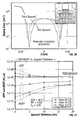
- FIG. 20shows an example of a reduction in junction abruptness as a result of different thicknesses for intermediate spacer 1908 .
- Junction leakage currentreduces as intermediate spacer 1908 thickness gets smaller.
- FIG. 21shows a comparison of sub-threshold current and junction leakage current for different thicknesses of intermediate spacer 1908 and different doses of Phosphorous. Significant reduction in junction leakage current can be obtained through modulation of intermediate spacer 1908 thickness and Phosphorous dose. For intermediate spacer 1908 thicknesses down to 5 nanometers, there is no significant affect on sub-threshold current.
- FIG. 22shows a comparison of DIBL and ⁇ Vt for different thicknesses of intermediate spacer 1908 .
- thicknesses of intermediate spacer 1908 down to 5 nanometersonly minor penalties in DIBL and ⁇ Vt are seen, insignificant to the overall gain obtained through the reduction of junction leakage for the transistor device.
- Table Iprovides a comparison of exemplary conditions in a two offset spacer implementation versus a three offset spacer implementation.
- use of an intermediate offset spaceroffers a large advantage in junction leakage current outweighing the small loss in DIBL and ⁇ Vt.
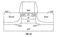
- FIG. 23shows an exemplary solution to this problem.
- a deep implantis performed prior to the source/drain region 2302 implant.
- a p-type-forming deep implant dopantsuch as Boron
- a n-type-forming deep implant dopantsuch as Phosphorous or Arsenic
- This implantforms a compensation layer 2304 preferably in alignment with the source/drain regions, to prevent the source/drain implants from diffusing too deep or getting too close to each other.
- Compensation layer 2304can be formed using ion implant using doses that are consistent with the doses selected for the source/drain implants, and energies that are either consistent with or slightly higher than the energies for the source/drain implants. Compensation layer 2304 implant is preferably angled to help ensure placement of compensation 2304 at the desired location. Other aspects of specific recipes are tailored using conventional methods for the given dopant species. Note that compensation layer 2304 can be used in the context of a selective epitaxially formed source and drain structure as well. Compensation layer 2304 should have a peak near the bottom of the source/drain region and form a barrier to prevent the diffusion of the source and drain. In addition to preventing the loss of back gate control, this process can be easily implemented as a single implant step with no additional masking step or thermal process required. With the compensation layer 2304 being relatively deep, there is no effect on the channel layer. Compensation layer 2304 has a deeper and slower profile having minimal impact on junction leakage current.
- the dLDD technique, the Phosphorous grading technique, the intermediate spacer technique, and the compensation layer technique discussed abovemay be performed alone or in any combination with each other for fabrication of a transistor device.
Landscapes
- Insulated Gate Type Field-Effect Transistor (AREA)
Abstract
Description
| TABLE I | ||
| Two Spacer Usage | Three | |
| Intermediate | ||
| 0 nm (total | 7 nm to 12 nm | |
| Spacer thickness | thickness of two | (assuming that |
| spacers is | when added to | |
| typically 19 nm) | first spacer and | |
| third spacer, | ||
| total spacer | ||
| thickness equals | ||
| 19 nm) | ||
| 2 × 10¹³ | atoms/ | 7 × 10¹³ | atoms/cm2 | |
| Junction Leakage | 284 | ρA/μm | 25.1 | ρA/μm |
| (10× gain) |
| VTSAT | 202 | mV | 190 | mV |
| VTLIN | 240 | mV | 232 | mV |
| DIBL | 38 | mV | 42 | mV |
| (11% loss) |
| σVTLIN | 3.24 | mV | 3.38 | mV |
| (4.3% loss) | |||
Claims (13)
Priority Applications (3)
| Application Number | Priority Date | Filing Date | Title |
|---|---|---|---|
| US13/725,152US8883600B1 (en) | 2011-12-22 | 2012-12-21 | Transistor having reduced junction leakage and methods of forming thereof |
| US14/534,595US9196727B2 (en) | 2011-12-22 | 2014-11-06 | High uniformity screen and epitaxial layers for CMOS devices |
| US14/808,122US9368624B2 (en) | 2011-12-22 | 2015-07-24 | Method for fabricating a transistor with reduced junction leakage current |
Applications Claiming Priority (2)
| Application Number | Priority Date | Filing Date | Title |
|---|---|---|---|
| US201161579142P | 2011-12-22 | 2011-12-22 | |
| US13/725,152US8883600B1 (en) | 2011-12-22 | 2012-12-21 | Transistor having reduced junction leakage and methods of forming thereof |
Related Child Applications (1)
| Application Number | Title | Priority Date | Filing Date |
|---|---|---|---|
| US14/534,595DivisionUS9196727B2 (en) | 2011-12-22 | 2014-11-06 | High uniformity screen and epitaxial layers for CMOS devices |
Publications (1)
| Publication Number | Publication Date |
|---|---|
| US8883600B1true US8883600B1 (en) | 2014-11-11 |
Family
ID=51845730
Family Applications (3)
| Application Number | Title | Priority Date | Filing Date |
|---|---|---|---|
| US13/725,152Active2033-01-07US8883600B1 (en) | 2011-12-22 | 2012-12-21 | Transistor having reduced junction leakage and methods of forming thereof |
| US14/534,595Expired - Fee RelatedUS9196727B2 (en) | 2011-12-22 | 2014-11-06 | High uniformity screen and epitaxial layers for CMOS devices |
| US14/808,122ActiveUS9368624B2 (en) | 2011-12-22 | 2015-07-24 | Method for fabricating a transistor with reduced junction leakage current |
Family Applications After (2)
| Application Number | Title | Priority Date | Filing Date |
|---|---|---|---|
| US14/534,595Expired - Fee RelatedUS9196727B2 (en) | 2011-12-22 | 2014-11-06 | High uniformity screen and epitaxial layers for CMOS devices |
| US14/808,122ActiveUS9368624B2 (en) | 2011-12-22 | 2015-07-24 | Method for fabricating a transistor with reduced junction leakage current |
Country Status (1)
| Country | Link |
|---|---|
| US (3) | US8883600B1 (en) |
Cited By (3)
| Publication number | Priority date | Publication date | Assignee | Title |
|---|---|---|---|---|
| US20170301694A1 (en)* | 2013-01-18 | 2017-10-19 | Renesas Electronics Corporation | Semiconductor device with silicon layer containing carbon |
| CN112908854A (en)* | 2021-01-28 | 2021-06-04 | 上海华力集成电路制造有限公司 | Method for reducing punch-through effect and component variation of N-tube short-channel component |
| US20210202708A1 (en)* | 2013-06-27 | 2021-07-01 | Taiwan Semiconductor Manufacturing Company, Ltd. | Semiconductor device having multiple wells and method of making |
Families Citing this family (5)
| Publication number | Priority date | Publication date | Assignee | Title |
|---|---|---|---|---|
| US9773733B2 (en) | 2015-03-26 | 2017-09-26 | Mie Fujitsu Semiconductor Limited | Semiconductor device |
| US9768254B2 (en) | 2015-07-30 | 2017-09-19 | International Business Machines Corporation | Leakage-free implantation-free ETSOI transistors |
| JP7091675B2 (en)* | 2018-01-26 | 2022-06-28 | ユナイテッド・セミコンダクター・ジャパン株式会社 | Semiconductor equipment |
| JP7115037B2 (en) | 2018-05-25 | 2022-08-09 | ユナイテッド・セミコンダクター・ジャパン株式会社 | semiconductor equipment |
| DE102019206494A1 (en) | 2019-05-06 | 2020-11-12 | MAX-PLANCK-Gesellschaft zur Förderung der Wissenschaften e.V. | DEPFET transistor and method of making a DEPFET transistor |
Citations (455)
| Publication number | Priority date | Publication date | Assignee | Title |
|---|---|---|---|---|
| US3958266A (en) | 1974-04-19 | 1976-05-18 | Rca Corporation | Deep depletion insulated gate field effect transistors |
| US4000504A (en) | 1975-05-12 | 1976-12-28 | Hewlett-Packard Company | Deep channel MOS transistor |
| US4021835A (en) | 1974-01-25 | 1977-05-03 | Hitachi, Ltd. | Semiconductor device and a method for fabricating the same |
| US4242691A (en) | 1978-09-18 | 1980-12-30 | Mitsubishi Denki Kabushiki Kaisha | MOS Semiconductor device |
| US4276095A (en) | 1977-08-31 | 1981-06-30 | International Business Machines Corporation | Method of making a MOSFET device with reduced sensitivity of threshold voltage to source to substrate voltage variations |
| US4315781A (en) | 1980-04-23 | 1982-02-16 | Hughes Aircraft Company | Method of controlling MOSFET threshold voltage with self-aligned channel stop |
| JPS59193066U (en) | 1983-06-08 | 1984-12-21 | 三菱電機株式会社 | Elevator security TV camera |
| US4518926A (en) | 1982-12-20 | 1985-05-21 | At&T Bell Laboratories | Gate-coupled field-effect transistor pair amplifier |
| US4559091A (en) | 1984-06-15 | 1985-12-17 | Regents Of The University Of California | Method for producing hyperabrupt doping profiles in semiconductors |
| US4578128A (en) | 1984-12-03 | 1986-03-25 | Ncr Corporation | Process for forming retrograde dopant distributions utilizing simultaneous outdiffusion of dopants |
| US4617066A (en) | 1984-11-26 | 1986-10-14 | Hughes Aircraft Company | Process of making semiconductors having shallow, hyperabrupt doped regions by implantation and two step annealing |
| US4662061A (en) | 1985-02-27 | 1987-05-05 | Texas Instruments Incorporated | Method for fabricating a CMOS well structure |
| US4761384A (en) | 1986-06-10 | 1988-08-02 | Siemens Aktiengesellschaft | Forming retrograde twin wells by outdiffusion of impurity ions in epitaxial layer followed by CMOS device processing |
| US4780748A (en) | 1986-06-06 | 1988-10-25 | American Telephone & Telegraph Company, At&T Bell Laboratories | Field-effect transistor having a delta-doped ohmic contact |
| US4819043A (en) | 1985-11-29 | 1989-04-04 | Hitachi, Ltd. | MOSFET with reduced short channel effect |
| EP0312237A2 (en) | 1987-10-13 | 1989-04-19 | AT&T Corp. | Interface charge enhancement in delta-doped heterostructure |
| US4885477A (en) | 1987-06-08 | 1989-12-05 | U.S. Philips Corporation | Differential amplifier and current sensing circuit including such an amplifier |
| US4908681A (en) | 1980-04-30 | 1990-03-13 | Sanyo Electric Co., Ltd. | Insulated gate field effect transistor with buried layer |
| US4945254A (en) | 1986-03-19 | 1990-07-31 | The Secretary of State for Defence in Her Britannic Majesty's Government for the United Kingdom of Great Britain and Northern Ireland | Method and apparatus for monitoring surface layer growth |
| US4956311A (en) | 1989-06-27 | 1990-09-11 | National Semiconductor Corporation | Double-diffused drain CMOS process using a counterdoping technique |
| US5034337A (en) | 1989-02-10 | 1991-07-23 | Texas Instruments Incorporated | Method of making an integrated circuit that combines multi-epitaxial power transistors with logic/analog devices |
| US5144378A (en) | 1990-03-06 | 1992-09-01 | Fujitsu Limited | High electron mobility transistor |
| US5156990A (en) | 1986-07-23 | 1992-10-20 | Texas Instruments Incorporated | Floating-gate memory cell with tailored doping profile |
| US5156989A (en) | 1988-11-08 | 1992-10-20 | Siliconix, Incorporated | Complementary, isolated DMOS IC technology |
| US5166765A (en) | 1991-08-26 | 1992-11-24 | At&T Bell Laboratories | Insulated gate field-effect transistor with pulse-shaped doping |
| US5208473A (en) | 1989-11-29 | 1993-05-04 | Mitsubishi Denki Kabushiki Kaisha | Lightly doped MISFET with reduced latchup and punchthrough |
| US5294821A (en) | 1990-10-09 | 1994-03-15 | Seiko Epson Corporation | Thin-film SOI semiconductor device having heavily doped diffusion regions beneath the channels of transistors |
| US5298763A (en) | 1992-11-02 | 1994-03-29 | Motorola, Inc. | Intrinsically doped semiconductor structure and method for making |
| EP0274278B1 (en) | 1987-01-05 | 1994-05-25 | Seiko Instruments Inc. | MOS field effect transistor and method of manufacturing the same |
| US5369288A (en) | 1992-05-08 | 1994-11-29 | Fujitsu Limited | Semiconductor device for switching a ballistic flow of carriers |
| US5373186A (en) | 1984-11-19 | 1994-12-13 | Max-Planck Gesellschaft Zur Foerderung Der Wissenschaften E.V. | Bipolar transistor with monoatomic base layer between emitter and collector layers |
| US5384476A (en) | 1979-08-25 | 1995-01-24 | Zaidan Hojin Handotai Kenkyu Shinkokai | Short channel MOSFET with buried anti-punch through region |
| US5426328A (en) | 1992-09-21 | 1995-06-20 | Siliconix Incorporated | BICDMOS structures |
| US5444008A (en) | 1993-09-24 | 1995-08-22 | Vlsi Technology, Inc. | High-performance punchthrough implant method for MOS/VLSI |
| EP0531621A3 (en) | 1991-09-12 | 1995-08-30 | Po Hang Iron & Steel | Process for formation of delta-doped quantum well field effect transistor |
| US5552332A (en) | 1995-06-02 | 1996-09-03 | Motorola, Inc. | Process for fabricating a MOSFET device having reduced reverse short channel effects |
| US5559368A (en) | 1994-08-30 | 1996-09-24 | The Regents Of The University Of California | Dynamic threshold voltage mosfet having gate to body connection for ultra-low voltage operation |
| US5608253A (en) | 1995-03-22 | 1997-03-04 | Advanced Micro Devices Inc. | Advanced transistor structures with optimum short channel controls for high density/high performance integrated circuits |
| US5622880A (en) | 1994-08-18 | 1997-04-22 | Sun Microsystems, Inc. | Method of making a low power, high performance junction transistor |
| US5624863A (en) | 1995-07-17 | 1997-04-29 | Micron Technology, Inc. | Semiconductor processing method of forming complementary N-type doped and P-type doped active regions within a semiconductor substrate |
| US5625568A (en) | 1993-12-22 | 1997-04-29 | Vlsi Technology, Inc. | Method and apparatus for compacting integrated circuits with standard cell architectures |
| US5641980A (en) | 1995-06-16 | 1997-06-24 | Mitsubishi Denki Kabushiki Kaisha | Device having a high concentration region under the channel |
| US5663583A (en) | 1995-06-06 | 1997-09-02 | Hughes Aircraft Company | Low-noise and power ALGaPSb/GaInAs HEMTs and pseudomorpohic HEMTs on GaAs substrate |
| US5712501A (en) | 1995-10-10 | 1998-01-27 | Motorola, Inc. | Graded-channel semiconductor device |
| US5726562A (en) | 1995-09-07 | 1998-03-10 | Nec Corporation | Semiconductor device and power supply controller for same |
| US5726488A (en) | 1985-11-29 | 1998-03-10 | Hitachi, Ltd. | Semiconductor device having semiconductor elements formed in a retrograde well structure |
| US5731626A (en) | 1994-12-01 | 1998-03-24 | Lucent Technologies Inc. | Process for controlling dopant diffusion in a semiconductor layer and semiconductor layer formed thereby |
| US5736419A (en) | 1996-11-12 | 1998-04-07 | National Semiconductor Corporation | Method of fabricating a raised source/drain MOSFET using self-aligned POCl3 for doping gate/source/drain regions |
| US5754826A (en) | 1995-08-04 | 1998-05-19 | Synopsys, Inc. | CAD and simulation system for targeting IC designs to multiple fabrication processes |
| US5753555A (en) | 1995-11-22 | 1998-05-19 | Nec Corporation | Method for forming semiconductor device |
| US5756365A (en) | 1992-10-30 | 1998-05-26 | Kabushiki Kaisha Toshiba | Method of manufacturing MOS-type semiconductor device having electrode structure capable of coping with short-channel effects |
| US5763921A (en) | 1991-10-22 | 1998-06-09 | Mitsubishi Denki Kabushiki Kaisha | Semiconductor device including retrograde well structure with suppressed substrate bias effects |
| US5847419A (en) | 1996-09-17 | 1998-12-08 | Kabushiki Kaisha Toshiba | Si-SiGe semiconductor device and method of fabricating the same |
| US5856003A (en) | 1997-11-17 | 1999-01-05 | Taiwan Semiconductor Manufacturing Company, Ltd. | Method for forming pseudo buried layer for sub-micron bipolar or BiCMOS device |
| US5861334A (en) | 1995-08-07 | 1999-01-19 | Hyundai Electronics Industries Co., | Method for fabricating semiconductor device having a buried channel |
| US5885876A (en) | 1996-02-07 | 1999-03-23 | Thunderbird Technologies, Inc. | Methods of fabricating short channel fermi-threshold field effect transistors including drain field termination region |
| US5889315A (en) | 1994-08-18 | 1999-03-30 | National Semiconductor Corporation | Semiconductor structure having two levels of buried regions |
| US5895954A (en) | 1997-03-27 | 1999-04-20 | Mitsubishi Denki Kabushiki Kaisha | Field effect transistor with impurity concentration peak under gate electrode |
| US5918129A (en) | 1997-02-25 | 1999-06-29 | Advanced Micro Devices, Inc. | Method of channel doping using diffusion from implanted polysilicon |
| US5923987A (en) | 1997-06-30 | 1999-07-13 | Sun Microsystems, Inc. | Method for forming MOS devices with retrograde pocket regions and counter dopant regions at the substrate surface |
| US5923067A (en) | 1997-04-04 | 1999-07-13 | International Business Machines Corporation | 3-D CMOS-on-SOI ESD structure and method |
| US5936868A (en) | 1997-03-06 | 1999-08-10 | Harris Corporation | Method for converting an integrated circuit design for an upgraded process |
| US5946214A (en) | 1997-07-11 | 1999-08-31 | Advanced Micro Devices | Computer implemented method for estimating fabrication yield for semiconductor integrated circuit including memory blocks with redundant rows and/or columns |
| US5985705A (en) | 1998-06-30 | 1999-11-16 | Lsi Logic Corporation | Low threshold voltage MOS transistor and method of manufacture |
| US5989963A (en) | 1997-07-21 | 1999-11-23 | Advanced Micro Devices, Inc. | Method for obtaining a steep retrograde channel profile |
| US6001695A (en) | 1998-03-02 | 1999-12-14 | Texas Instruments - Acer Incorporated | Method to form ultra-short channel MOSFET with a gate-side airgap structure |
| US6020227A (en) | 1995-09-12 | 2000-02-01 | National Semiconductor Corporation | Fabrication of multiple field-effect transistor structure having local threshold-adjust doping |
| US6060345A (en) | 1997-04-21 | 2000-05-09 | Advanced Micro Devices, Inc. | Method of making NMOS and PMOS devices with reduced masking steps |
| US6060364A (en) | 1999-03-02 | 2000-05-09 | Advanced Micro Devices, Inc. | Fast Mosfet with low-doped source/drain |
| US6066533A (en) | 1998-09-29 | 2000-05-23 | Advanced Micro Devices, Inc. | MOS transistor with dual metal gate structure |
| US6072217A (en) | 1998-06-11 | 2000-06-06 | Sun Microsystems, Inc. | Tunable threshold SOI device using isolated well structure for back gate |
| US6088518A (en) | 1998-01-30 | 2000-07-11 | Aspec Technology, Inc. | Method and system for porting an integrated circuit layout from a reference process to a target process |
| US6087210A (en) | 1998-06-05 | 2000-07-11 | Hyundai Electronics Industries | Method of manufacturing a CMOS Transistor |
| US6087691A (en) | 1997-02-04 | 2000-07-11 | Mitsubishi Denki Kabushiki Kaisha | Semiconductor device having lower minority carrier noise |
| US6091286A (en) | 1994-02-14 | 2000-07-18 | Philips Electronics North America Corporation | Fully integrated reference circuit having controlled temperature dependence |
| US6096611A (en) | 1998-03-13 | 2000-08-01 | Texas Instruments - Acer Incorporated | Method to fabricate dual threshold CMOS circuits |
| US6103562A (en) | 1998-01-14 | 2000-08-15 | Lg Semicon Co., Ltd. | Method of making semiconductor device with decreased channel width and constant threshold voltage |
| US6121153A (en) | 1994-08-29 | 2000-09-19 | Fujitsu Limited | Semiconductor device having a regrowth crystal region |
| US6147383A (en) | 1995-03-10 | 2000-11-14 | Sony Corporation | LDD buried channel field effect semiconductor device and manufacturing method |
| US6153920A (en) | 1994-12-01 | 2000-11-28 | Lucent Technologies Inc. | Process for controlling dopant diffusion in a semiconductor layer and semiconductor device formed thereby |
| US6157073A (en) | 1997-09-29 | 2000-12-05 | Stmicroelectronics S.A. | Isolation between power supplies of an analog-digital circuit |
| US6175582B1 (en) | 1997-11-26 | 2001-01-16 | Mitsui Chemicals Inc. | Semiconductor laser device |
| US6184112B1 (en) | 1998-12-02 | 2001-02-06 | Advanced Micro Devices, Inc. | Method of forming a MOSFET transistor with a shallow abrupt retrograde dopant profile |
| US6190979B1 (en) | 1999-07-12 | 2001-02-20 | International Business Machines Corporation | Method for fabricating dual workfunction devices on a semiconductor substrate using counter-doping and gapfill |
| US6194259B1 (en) | 1997-06-27 | 2001-02-27 | Advanced Micro Devices, Inc. | Forming retrograde channel profile and shallow LLDD/S-D extensions using nitrogen implants |
| US6198157B1 (en) | 1997-02-26 | 2001-03-06 | Hitachi, Ltd. | Semiconductor device having buried boron and carbon regions |
| US6218895B1 (en) | 1997-06-20 | 2001-04-17 | Intel Corporation | Multiple well transistor circuits having forward body bias |
| US6218892B1 (en) | 1997-06-20 | 2001-04-17 | Intel Corporation | Differential circuits employing forward body bias |
| US6221724B1 (en) | 1998-11-06 | 2001-04-24 | Advanced Micro Devices, Inc. | Method of fabricating an integrated circuit having punch-through suppression |
| US6232164B1 (en) | 1999-05-24 | 2001-05-15 | Taiwan Semiconductor Manufacturing Company | Process of making CMOS device structure having an anti-SCE block implant |
| US6235597B1 (en) | 1999-08-06 | 2001-05-22 | International Business Machines Corporation | Semiconductor structure having reduced silicide resistance between closely spaced gates and method of fabrication |
| US6245618B1 (en) | 1999-02-03 | 2001-06-12 | Advanced Micro Devices, Inc. | Mosfet with localized amorphous region with retrograde implantation |
| US6268640B1 (en) | 1999-08-12 | 2001-07-31 | International Business Machines Corporation | Forming steep lateral doping distribution at source/drain junctions |
| US6271070B2 (en) | 1997-12-25 | 2001-08-07 | Matsushita Electronics Corporation | Method of manufacturing semiconductor device |
| US6271551B1 (en) | 1995-12-15 | 2001-08-07 | U.S. Philips Corporation | Si-Ge CMOS semiconductor device |
| EP0683515B1 (en) | 1994-05-17 | 2001-08-16 | Samsung Electronics Co., Ltd. | Method of manufacturing a CMOS device |
| US20010014495A1 (en) | 1999-01-27 | 2001-08-16 | Bin Yu | Method for forming super-steep retrograded channel (SSRC) for cmos transistor using rapid laser annealing to reduce thermal budget |
| US6288429B1 (en) | 1996-12-04 | 2001-09-11 | Sharp Kabushiki Kaisha | Semiconductor device |
| US6297132B1 (en) | 2000-02-07 | 2001-10-02 | Chartered Semiconductor Manufacturing Ltd. | Process to control the lateral doping profile of an implanted channel region |
| US6300177B1 (en) | 2001-01-25 | 2001-10-09 | Chartered Semiconductor Manufacturing Inc. | Method to form transistors with multiple threshold voltages (VT) using a combination of different work function gate materials |
| US6313489B1 (en) | 1999-11-16 | 2001-11-06 | Philips Electronics North America Corporation | Lateral thin-film silicon-on-insulator (SOI) device having a lateral drift region with a retrograde doping profile, and method of making such a device |
| US6320222B1 (en) | 1998-09-01 | 2001-11-20 | Micron Technology, Inc. | Structure and method for reducing threshold voltage variations due to dopant fluctuations |
| US6319799B1 (en) | 2000-05-09 | 2001-11-20 | Board Of Regents, The University Of Texas System | High mobility heterojunction transistor and method |
| US6323525B1 (en) | 1997-09-18 | 2001-11-27 | Kabushiki Kaisha Toshiba | MISFET semiconductor device having relative impurity concentration levels between layers |
| US6326666B1 (en) | 2000-03-23 | 2001-12-04 | International Business Machines Corporation | DTCMOS circuit having improved speed |
| US6335233B1 (en) | 1998-07-02 | 2002-01-01 | Samsung Electronics Co., Ltd. | Method for fabricating MOS transistor |
| US6358806B1 (en) | 2001-06-29 | 2002-03-19 | Lsi Logic Corporation | Silicon carbide CMOS channel |
| US20020042184A1 (en) | 2000-10-10 | 2002-04-11 | Mahalingam Nandakumar | Reduction in well implant channeling and resulting latchup characteristics in shallow trench ilolation by implanting wells through nitride |
| US6380019B1 (en) | 1998-11-06 | 2002-04-30 | Advanced Micro Devices, Inc. | Method of manufacturing a transistor with local insulator structure |
| US6391752B1 (en) | 2000-09-12 | 2002-05-21 | Taiwan Semiconductor Manufacturing, Co., Ltd. | Method of fabricating a silicon-on-insulator semiconductor device with an implanted ground plane |
| US6426260B1 (en) | 1997-12-02 | 2002-07-30 | Magepower Semiconductor Corp. | Switching speed improvement in DMO by implanting lightly doped region under gate |
| US6426279B1 (en) | 1999-08-18 | 2002-07-30 | Advanced Micro Devices, Inc. | Epitaxial delta doping for retrograde channel profile |
| US6432754B1 (en) | 2001-02-20 | 2002-08-13 | International Business Machines Corporation | Double SOI device with recess etch and epitaxy |
| US6444551B1 (en) | 2001-07-23 | 2002-09-03 | Taiwan Semiconductor Manufacturing Company | N-type buried layer drive-in recipe to reduce pits over buried antimony layer |
| US6444550B1 (en) | 1999-08-18 | 2002-09-03 | Advanced Micro Devices, Inc. | Laser tailoring retrograde channel profile in surfaces |
| US6449749B1 (en) | 1999-11-18 | 2002-09-10 | Pdf Solutions, Inc. | System and method for product yield prediction |
| US6461920B1 (en) | 1996-04-01 | 2002-10-08 | Mitsubishi Denki Kabushiki Kaisha | Semiconductor device and method of manufacturing the same |
| US6461928B2 (en) | 2000-05-23 | 2002-10-08 | Texas Instruments Incorporated | Methodology for high-performance, high reliability input/output devices and analog-compatible input/output and core devices using core device implants |
| US6472278B1 (en) | 1998-06-22 | 2002-10-29 | Motorola, Inc. | Method and apparatus for creating a voltage threshold in a FET |
| US6482714B1 (en) | 1999-02-24 | 2002-11-19 | Kabushiki Kaisha Toshiba | Semiconductor device and method of manufacturing the same |
| US6489224B1 (en) | 2001-05-31 | 2002-12-03 | Sun Microsystems, Inc. | Method for engineering the threshold voltage of a device using buried wells |
| US6492232B1 (en) | 1998-06-15 | 2002-12-10 | Motorola, Inc. | Method of manufacturing vertical semiconductor device |
| US6500739B1 (en) | 2001-06-14 | 2002-12-31 | Taiwan Semiconductor Manufacturing Company | Formation of an indium retrograde profile via antimony ion implantation to improve NMOS short channel effect |
| US6503801B1 (en) | 1999-08-18 | 2003-01-07 | Advanced Micro Devices, Inc. | Non-uniform channel profile via enhanced diffusion |
| US6503805B2 (en) | 1999-09-02 | 2003-01-07 | Micron Technology, Inc. | Channel implant through gate polysilicon |
| US20030006415A1 (en) | 2000-06-27 | 2003-01-09 | Toshiya Yokogawa | Semiconductor device |
| US6506640B1 (en) | 1999-09-24 | 2003-01-14 | Advanced Micro Devices, Inc. | Multiple channel implantation to form retrograde channel profile and to engineer threshold voltage and sub-surface punch-through |
| US6518623B1 (en) | 2000-06-09 | 2003-02-11 | Mitsubishi Denki Kabushiki Kaisha | Semiconductor device having a buried-channel MOS structure |
| US6521470B1 (en) | 2001-10-31 | 2003-02-18 | United Microelectronics Corp. | Method of measuring thickness of epitaxial layer |
| US6534373B1 (en) | 2001-03-26 | 2003-03-18 | Advanced Micro Devices, Inc. | MOS transistor with reduced floating body effect |
| US6541328B2 (en) | 2001-02-19 | 2003-04-01 | Samsung Electronics Co., Ltd. | Method of fabricating metal oxide semiconductor transistor with lightly doped impurity regions formed after removing spacers used for defining higher density impurity regions |
| US6541829B2 (en) | 1999-12-03 | 2003-04-01 | Kabushiki Kaisha Toshiba | Semiconductor device and method of manufacturing the same |
| US6548842B1 (en) | 2000-03-31 | 2003-04-15 | National Semiconductor Corporation | Field-effect transistor for alleviating short-channel effects |
| US6551885B1 (en) | 2001-02-09 | 2003-04-22 | Advanced Micro Devices, Inc. | Low temperature process for a thin film transistor |
| US6573129B2 (en) | 1999-08-06 | 2003-06-03 | Raytheon Company | Gate electrode formation in double-recessed transistor by two-step etching |
| US6576535B2 (en) | 2001-04-11 | 2003-06-10 | Texas Instruments Incorporated | Carbon doped epitaxial layer for high speed CB-CMOS |
| US6600200B1 (en) | 1999-08-25 | 2003-07-29 | Infineon Technologies Ag | MOS transistor, method for fabricating a MOS transistor and method for fabricating two complementary MOS transistors |
| US6620671B1 (en) | 2001-05-01 | 2003-09-16 | Advanced Micro Devices, Inc. | Method of fabricating transistor having a single crystalline gate conductor |
| US20030173626A1 (en) | 2001-05-18 | 2003-09-18 | Burr James B. | Device including a resistive path to introduce an equivalent RC circuit |
| US6624488B1 (en) | 2000-08-07 | 2003-09-23 | Advanced Micro Devices, Inc. | Epitaxial silicon growth and usage of epitaxial gate insulator for low power, high performance devices |
| US6627473B1 (en) | 1999-11-16 | 2003-09-30 | Nec Compound Semiconductor Devices, Ltd. | Compound semiconductor device with delta doped layer under etching stopper layer for decreasing resistance between active layer and ohmic electrode and process of fabrication thereof |
| US20030183856A1 (en) | 2002-03-28 | 2003-10-02 | Karsten Wieczorek | Semiconductor device having a retrograde dopant profile in a channel region and method for fabricating the same |
| US6630710B1 (en) | 1998-09-29 | 2003-10-07 | Newport Fab, Llc | Elevated channel MOSFET |
| US20030215992A1 (en) | 2002-05-20 | 2003-11-20 | Sohn Yong Sun | Method for forming transistor of semiconductor device |
| US6662350B2 (en) | 2002-01-28 | 2003-12-09 | International Business Machines Corporation | FinFET layout generation |
| US6660605B1 (en) | 2002-11-12 | 2003-12-09 | Texas Instruments Incorporated | Method to fabricate optimal HDD with dual diffusion process to optimize transistor drive current junction capacitance, tunneling current and channel dopant loss |
| US6670260B1 (en) | 1998-11-06 | 2003-12-30 | Advanced Micro Devices, Inc. | Transistor with local insulator structure |
| US6693333B1 (en) | 2001-05-01 | 2004-02-17 | Advanced Micro Devices, Inc. | Semiconductor-on-insulator circuit with multiple work functions |
| JP2004087671A (en) | 2002-08-26 | 2004-03-18 | Sharp Corp | Semiconductor device and method of manufacturing the same |
| US20040075118A1 (en) | 2000-12-08 | 2004-04-22 | Bernd Heinemann | Layers in substrate wafers |
| US20040075143A1 (en) | 2000-01-07 | 2004-04-22 | Geum-Jong Bae | CMOS integrated circuit devices and substrates having buried silicon germanium layers therein and methods of forming same |
| US6730568B2 (en) | 2002-09-17 | 2004-05-04 | Hynix Semiconductor Inc. | Method for fabricating semiconductor device with ultra-shallow super-steep-retrograde epi-channel by boron-fluoride compound doping |
| US20040084731A1 (en) | 2001-03-29 | 2004-05-06 | Kabushiki Kaisha Toshiba | Semiconductor device comprising buried channel region and method for manufacturing the same |
| US20040087090A1 (en) | 2002-10-31 | 2004-05-06 | Grudowski Paul A. | Semiconductor fabrication process using transistor spacers of differing widths |
| US6743291B2 (en) | 2002-07-09 | 2004-06-01 | Chartered Semiconductor Manufacturing Ltd. | Method of fabricating a CMOS device with integrated super-steep retrograde twin wells using double selective epitaxial growth |
| US6743684B2 (en) | 2002-10-11 | 2004-06-01 | Texas Instruments Incorporated | Method to produce localized halo for MOS transistor |
| US6751519B1 (en) | 2001-10-25 | 2004-06-15 | Kla-Tencor Technologies Corporation | Methods and systems for predicting IC chip yield |
| US6753230B2 (en) | 2002-05-18 | 2004-06-22 | Hynix Semiconductor Inc. | Method for fabricating semiconductor device with ultra-shallow super-steep-retrograde epi-channel by decaborane doping |
| US20040126947A1 (en) | 2002-12-30 | 2004-07-01 | Hynix Semiconductor Inc. | pMOS device having ultra shallow super-steep-retrograde epi-channel with dual channel doping and method for fabricating the same |
| US6760900B2 (en) | 2001-12-03 | 2004-07-06 | Anadigics Inc. | Integrated circuits with scalable design |
| US6787424B1 (en) | 2001-02-09 | 2004-09-07 | Advanced Micro Devices, Inc. | Fully depleted SOI transistor with elevated source and drain |
| US20040175893A1 (en) | 2003-03-07 | 2004-09-09 | Applied Materials, Inc. | Apparatuses and methods for forming a substantially facet-free epitaxial film |
| US20040180488A1 (en) | 2003-03-13 | 2004-09-16 | Won-Ho Lee | Method for fabricating complementary metal oxide semiconductor image sensor |
| US6797553B2 (en) | 2000-10-24 | 2004-09-28 | International Business Machines Corporation | Method for making multiple threshold voltage FET using multiple work-function gate materials |
| US6797994B1 (en) | 2000-02-14 | 2004-09-28 | Raytheon Company | Double recessed transistor |
| US6797602B1 (en) | 2001-02-09 | 2004-09-28 | Advanced Micro Devices, Inc. | Method of manufacturing a semiconductor device with supersaturated source/drain extensions and metal silicide contacts |
| US6808994B1 (en) | 2003-06-17 | 2004-10-26 | Micron Technology, Inc. | Transistor structures and processes for forming same |
| US6808004B2 (en) | 2002-01-31 | 2004-10-26 | Tht Presses Inc. | Semi-solid molding method |
| US6813750B2 (en) | 2001-04-02 | 2004-11-02 | Kabushiki Kaisha Toshiba | Logic circuit design equipment and method for designing logic circuit for reducing leakage current |
| US6822297B2 (en) | 2001-06-07 | 2004-11-23 | Texas Instruments Incorporated | Additional n-type LDD/pocket implant for improving short-channel NMOS ESD robustness |
| US6821825B2 (en) | 2001-02-12 | 2004-11-23 | Asm America, Inc. | Process for deposition of semiconductor films |
| US6821852B2 (en) | 2001-02-13 | 2004-11-23 | Micron Technology, Inc. | Dual doped gates |
| US6831292B2 (en) | 2001-09-21 | 2004-12-14 | Amberwave Systems Corporation | Semiconductor structures employing strained material layers with defined impurity gradients and methods for fabricating same |
| US6835639B2 (en) | 2001-11-30 | 2004-12-28 | Texas Instruments Incorporated | Multiple work function gates |
| US6852602B2 (en) | 2001-01-31 | 2005-02-08 | Matsushita Electric Industrial Co., Ltd. | Semiconductor crystal film and method for preparation thereof |
| US6852603B2 (en) | 2001-12-12 | 2005-02-08 | Texas Instruments Incorporated | Fabrication of abrupt ultra-shallow junctions |
| US6891439B2 (en) | 2002-11-04 | 2005-05-10 | Advanced Micro Devices, Inc. | Circuit and a method for controlling the bias current in a switched capacitor circuit |
| US6893947B2 (en) | 2002-06-25 | 2005-05-17 | Freescale Semiconductor, Inc. | Advanced RF enhancement-mode FETs with improved gate properties |
| US20050106824A1 (en) | 2001-12-04 | 2005-05-19 | Carnera Alberto | Method for suppressing transient enhanced diffusion of dopants in silicon |
| US6900519B2 (en) | 2002-07-18 | 2005-05-31 | International Business Machines Corporation | Diffused extrinsic base and method for fabrication |
| US20050116282A1 (en) | 2003-12-02 | 2005-06-02 | Vishay-Siliconix | Closed cell trench metal-oxide-semiconductor field effect transistor |
| US6916698B2 (en) | 2002-04-19 | 2005-07-12 | International Business Machines Corporation | High performance CMOS device structure with mid-gap metal gate |
| US6917237B1 (en) | 2004-03-02 | 2005-07-12 | Intel Corporation | Temperature dependent regulation of threshold voltage |
| US6927463B2 (en) | 1996-06-28 | 2005-08-09 | Sharp Kabushiki Kaisha | Semiconductor device and method for fabricating the same |
| US6928128B1 (en) | 1999-05-03 | 2005-08-09 | Rambus Inc. | Clock alignment circuit having a self regulating voltage supply |
| US6930360B2 (en) | 2002-09-24 | 2005-08-16 | Kabushiki Kaisha Toshiba | Semiconductor device and manufacturing method of the same |
| US6930007B2 (en) | 2003-09-15 | 2005-08-16 | Texas Instruments Incorporated | Integration of pre-S/D anneal selective nitride/oxide composite cap for improving transistor performance |
| US6957163B2 (en) | 2002-04-24 | 2005-10-18 | Yoshiyuki Ando | Integrated circuits having post-silicon adjustment control |
| US6963090B2 (en) | 2003-01-09 | 2005-11-08 | Freescale Semiconductor, Inc. | Enhancement mode metal-oxide-semiconductor field effect transistor |
| US20050250289A1 (en) | 2002-10-30 | 2005-11-10 | Babcock Jeffrey A | Control of dopant diffusion from buried layers in bipolar integrated circuits |
| US20050280075A1 (en) | 2003-06-10 | 2005-12-22 | Fujitsu Limited | Semiconductor integrated circuit device having improved punch-through resistance and production method thereof, semiconductor integrated circuit device including a low-voltage transistor and a high-voltage transistor |
| US20060022270A1 (en) | 2004-07-30 | 2006-02-02 | International Business Machines Corporation | Ultra-thin body super-steep retrograde well (ssrw) fet devices |
| US6995397B2 (en) | 2001-09-14 | 2006-02-07 | Matsushita Electric Industrial Co., Ltd. | Semiconductor device |
| US7008836B2 (en) | 2003-03-28 | 2006-03-07 | Infineon Technologies Wireless Solutions Sweden Ab | Method to provide a triple well in an epitaxially based CMOS or BiCMOS process |
| US20060049464A1 (en) | 2004-09-03 | 2006-03-09 | Rao G R Mohan | Semiconductor devices with graded dopant regions |
| US7013359B1 (en) | 2001-12-21 | 2006-03-14 | Cypress Semiconductor Corporation | High speed memory interface system and method |
| US7015546B2 (en) | 2000-02-23 | 2006-03-21 | Semiconductor Research Corporation | Deterministically doped field-effect devices and methods of making same |
| US7015741B2 (en) | 2003-12-23 | 2006-03-21 | Intel Corporation | Adaptive body bias for clock skew compensation |
| US20060068555A1 (en) | 2004-09-30 | 2006-03-30 | International Business Machines Corporation | Structure and method for manufacturing MOSFET with super-steep retrograded island |
| US20060068586A1 (en) | 2004-09-17 | 2006-03-30 | Bedabrata Pain | Method for implementation of back-illuminated CMOS or CCD imagers |
| US7022559B2 (en) | 1998-09-30 | 2006-04-04 | Intel Corporation | MOSFET gate electrodes having performance tuned work functions and methods of making same |
| US20060071278A1 (en) | 2004-09-27 | 2006-04-06 | Fujitsu Limited | Semiconductor device and method for fabricating the same |
| US7036098B2 (en) | 2003-06-30 | 2006-04-25 | Sun Microsystems, Inc. | On-chip signal state duration measurement and adjustment |
| US7039881B2 (en) | 1999-12-08 | 2006-05-02 | Timothy James Regan | Modification of integrated circuits |
| US7038258B2 (en) | 2003-06-05 | 2006-05-02 | Texas Instruments Incorporated | Semiconductor device having a localized halo implant therein and method of manufacture therefor |
| US7045456B2 (en) | 2003-12-22 | 2006-05-16 | Texas Instruments Incorporated | MOS transistor gates with thin lower metal silicide and methods for making the same |
| US7057216B2 (en) | 2003-10-31 | 2006-06-06 | International Business Machines Corporation | High mobility heterojunction complementary field effect transistors and methods thereof |
| US7061058B2 (en) | 2003-12-01 | 2006-06-13 | Texas Instruments Incorporated | Forming a retrograde well in a transistor to enhance performance of the transistor |
| US7064399B2 (en) | 2000-09-15 | 2006-06-20 | Texas Instruments Incorporated | Advanced CMOS using super steep retrograde wells |
| US7071103B2 (en) | 2004-07-30 | 2006-07-04 | International Business Machines Corporation | Chemical treatment to retard diffusion in a semiconductor overlayer |
| US20060154428A1 (en) | 2005-01-12 | 2006-07-13 | International Business Machines Corporation | Increasing doping of well compensating dopant region according to increasing gate length |
| US7078325B2 (en) | 2000-07-12 | 2006-07-18 | Infineon Technologies Ag | Process for producing a doped semiconductor substrate |
| US7089513B2 (en) | 2004-03-19 | 2006-08-08 | International Business Machines Corporation | Integrated circuit design for signal integrity, avoiding well proximity effects |
| US7089515B2 (en) | 2004-03-09 | 2006-08-08 | International Business Machines Corporation | Threshold voltage roll-off compensation using back-gated MOSFET devices for system high-performance and low standby power |
| US7091093B1 (en) | 1999-09-17 | 2006-08-15 | Matsushita Electric Industrial Co., Ltd. | Method for fabricating a semiconductor device having a pocket dopant diffused layer |
| US7105399B1 (en) | 2004-12-07 | 2006-09-12 | Advanced Micro Devices, Inc. | Selective epitaxial growth for tunable channel thickness |
| US20060203581A1 (en) | 2005-03-10 | 2006-09-14 | Joshi Rajiv V | Efficient method and computer program for modeling and improving static memory performance across process variations and environmental conditions |
| US7109099B2 (en) | 2003-10-17 | 2006-09-19 | Chartered Semiconductor Manufacturing Ltd. | End of range (EOR) secondary defect engineering using substitutional carbon doping |
| US20060223248A1 (en) | 2005-03-29 | 2006-10-05 | Texas Instruments Incorporated | N+ poly on high-k dielectric for semiconductor devices |
| US20060220114A1 (en) | 2005-03-30 | 2006-10-05 | Fujitsu Limited | Semiconductor device and manufacturing method thereof |
| US7119381B2 (en) | 2004-07-30 | 2006-10-10 | Freescale Semiconductor, Inc. | Complementary metal-oxide-semiconductor field effect transistor structure having ion implant in only one of the complementary devices |
| US7122411B2 (en) | 2000-08-31 | 2006-10-17 | Micron Technology, Inc | SOI device with reduced drain induced barrier lowering |
| US7127687B1 (en) | 2003-10-14 | 2006-10-24 | Sun Microsystems, Inc. | Method and apparatus for determining transistor sizes |
| US7132323B2 (en) | 2003-11-14 | 2006-11-07 | International Business Machines Corporation | CMOS well structure and method of forming the same |
| EP0889502B1 (en) | 1997-06-30 | 2006-12-20 | International Business Machines Corporation | Semiconductor structure with abrupt doping profile |
| US7169675B2 (en) | 2004-07-07 | 2007-01-30 | Chartered Semiconductor Manufacturing, Ltd | Material architecture for the fabrication of low temperature transistor |
| US7170120B2 (en) | 2005-03-31 | 2007-01-30 | Intel Corporation | Carbon nanotube energy well (CNEW) field effect transistor |
| US7176137B2 (en) | 2003-05-09 | 2007-02-13 | Taiwan Semiconductor Manufacturing Co., Ltd. | Method for multiple spacer width control |
| US20070040222A1 (en) | 2005-06-15 | 2007-02-22 | Benjamin Van Camp | Method and apparatus for improved ESD performance |
| US7189627B2 (en) | 2004-08-19 | 2007-03-13 | Texas Instruments Incorporated | Method to improve SRAM performance and stability |
| US7202517B2 (en) | 2003-07-18 | 2007-04-10 | Interuniversitair Microelektronica Centrum (Imec Vzw) | Multiple gate semiconductor device and method for forming same |
| US7208354B2 (en) | 2003-07-23 | 2007-04-24 | Asm America, Inc. | Deposition of silicon germanium on silicon-on-insulator structures and bulk substrates |
| US7211871B2 (en) | 2003-12-31 | 2007-05-01 | Dongbu Electronics, Co., Ltd. | Transistors of semiconductor devices and methods of fabricating the same |
| US7221021B2 (en) | 2004-06-25 | 2007-05-22 | Taiwan Semiconductor Manufacturing Co., Ltd. | Method of forming high voltage devices with retrograde well |
| US7226843B2 (en) | 2002-09-30 | 2007-06-05 | Intel Corporation | Indium-boron dual halo MOSFET |
| US7226833B2 (en) | 2004-10-29 | 2007-06-05 | Freescale Semiconductor, Inc. | Semiconductor device structure and method therefor |
| US7230680B2 (en) | 2002-12-20 | 2007-06-12 | Kabushiki Kaisha Toshiba | Wafer flatness evaluation method, wafer flatness evaluation apparatus carrying out the evaluation method, wafer manufacturing method using the evaluation method, wafer quality assurance method using the evaluation method, semiconductor device manufacturing method using the evaluation method and semiconductor device manufacturing method using a wafer evaluated by the evaluation method |
| US7235822B2 (en) | 2003-12-30 | 2007-06-26 | Infineon Technologies Ag | Transistor with silicon and carbon layer in the channel region |
| US7256639B1 (en) | 2004-02-02 | 2007-08-14 | Transmeta Corporation | Systems and methods for integrated circuits comprising multiple body bias domains |
| US7260562B2 (en) | 2003-06-30 | 2007-08-21 | Intel Corporation | Solutions for constraint satisfaction problems requiring multiple constraints |
| US7259428B2 (en) | 2004-08-05 | 2007-08-21 | Kabushiki Kaisha Toshiba | Semiconductor device using SOI structure having a triple-well region |
| US20070212861A1 (en) | 2006-03-07 | 2007-09-13 | International Business Machines Corporation | Laser surface annealing of antimony doped amorphized semiconductor region |
| US20070238253A1 (en) | 2006-04-10 | 2007-10-11 | Tucker Jesse B | Semiconductor transistors having reduced channel widths and methods of fabricating same |
| US7294877B2 (en) | 2003-03-28 | 2007-11-13 | Nantero, Inc. | Nanotube-on-gate FET structures and applications |
| US7297994B2 (en) | 2002-03-28 | 2007-11-20 | Advanced Micro Devices, Inc. | Semiconductor device having a retrograde dopant profile in a channel region |
| US7301208B2 (en) | 2004-08-04 | 2007-11-27 | Matsushita Electric Industrial Co., Ltd. | Semiconductor device and method for fabricating the same |
| US7304350B2 (en) | 2005-09-05 | 2007-12-04 | Matsushita Electric Industrial Co., Ltd. | Threshold voltage control layer in a semiconductor device |
| US7307471B2 (en) | 2005-08-26 | 2007-12-11 | Texas Instruments Incorporated | Adaptive voltage control and body bias for performance and energy optimization |
| US7323754B2 (en) | 2003-04-10 | 2008-01-29 | Fujitsu Limited | Semiconductor device and its manufacture method |
| US7332439B2 (en) | 2004-09-29 | 2008-02-19 | Intel Corporation | Metal gate transistors with epitaxial source and drain regions |
| US20080067589A1 (en) | 2006-09-20 | 2008-03-20 | Akira Ito | Transistor having reduced channel dopant fluctuation |
| US7348629B2 (en) | 2006-04-20 | 2008-03-25 | International Business Machines Corporation | Metal gated ultra short MOSFET devices |
| US7354833B2 (en) | 2005-06-10 | 2008-04-08 | Taiwan Semiconductor Manufacturing Co., Ltd. | Method for improving threshold voltage stability of a MOS device |
| US20080108208A1 (en) | 2006-11-08 | 2008-05-08 | Varian Semiconductor Equipment Associates, Inc. | Techniques for forming shallow junctions |
| US7380225B2 (en) | 2006-03-14 | 2008-05-27 | International Business Machines Corporation | Method and computer program for efficient cell failure rate estimation in cell arrays |
| US7398497B2 (en) | 2001-07-11 | 2008-07-08 | Fujitsu Limited | Electronic circuit designing method apparatus for designing an electronic circuit, and storage medium for storing an electronic circuit designing method |
| US20080169493A1 (en) | 2007-01-15 | 2008-07-17 | Lee Jin-Woo | Semiconductor devices and dynamic random access memories having a retrograde region and methods of forming the same |
| US20080169516A1 (en) | 2007-01-17 | 2008-07-17 | Taiwan Semiconductor Manufacturing Co., Ltd. | Semiconductor devices for alleviating well proximity effects |
| US7402207B1 (en) | 2004-05-05 | 2008-07-22 | Advanced Micro Devices, Inc. | Method and apparatus for controlling the thickness of a selective epitaxial growth layer |
| US7402872B2 (en) | 2004-11-18 | 2008-07-22 | Intel Corporation | Method for forming an integrated circuit |
| US20080197439A1 (en) | 2004-11-08 | 2008-08-21 | Alfred Goerlach | Semiconductor Device And Method For Manufacturing Same |
| US7416605B2 (en) | 2007-01-08 | 2008-08-26 | Freescale Semiconductor, Inc. | Anneal of epitaxial layer in a semiconductor device |
| US20080227250A1 (en) | 2007-03-15 | 2008-09-18 | Pushkar Ranade | CMOS device with dual-EPI channels and self-aligned contacts |
| US7427788B2 (en) | 2004-10-28 | 2008-09-23 | Samsung Electronics Co., Ltd. | Multi bridge channel field effect transistors with nano-wire channels and methods of manufacturing the same |
| US20080237661A1 (en) | 2007-03-30 | 2008-10-02 | Pushkar Ranade | Ultra-abrupt semiconductor junction profile |
| US20080258198A1 (en) | 2005-04-29 | 2008-10-23 | International Business Machines Corporation | Stabilization of flatband voltages and threshold voltages in hafnium oxide based silicon transistors for cmos |
| US7442971B2 (en) | 2004-07-30 | 2008-10-28 | Advanced Micro Devices, Inc. | Self-biasing transistor structure and an SRAM cell having less than six transistors |
| US20080272409A1 (en) | 2007-05-03 | 2008-11-06 | Dsm Solutions, Inc.; | JFET Having a Step Channel Doping Profile and Method of Fabrication |
| US7449733B2 (en) | 2005-11-09 | 2008-11-11 | Kabushiki Kaisha Toshiba | Semiconductor device and method of fabricating the same |
| JP4186774B2 (en) | 2003-09-25 | 2008-11-26 | 沖電気工業株式会社 | Information extraction apparatus, information extraction method, and program |
| US7462908B2 (en) | 2004-07-14 | 2008-12-09 | International Rectifier Corporation | Dynamic deep depletion field effect transistor |
| US7469164B2 (en) | 2006-06-26 | 2008-12-23 | Nanometrics Incorporated | Method and apparatus for process control with in-die metrology |
| US7470593B2 (en) | 2004-12-29 | 2008-12-30 | Hynix Semiconductor Inc. | Method for manufacturing a cell transistor of a semiconductor memory device |
| EP1450394B1 (en) | 2002-07-11 | 2009-01-07 | Panasonic Corporation | Semiconductor device and method for manufacturing same |
| US7487474B2 (en) | 2003-01-02 | 2009-02-03 | Pdf Solutions, Inc. | Designing an integrated circuit to improve yield using a variant design element |
| US7485536B2 (en) | 2005-12-30 | 2009-02-03 | Intel Corporation | Abrupt junction formation by atomic layer epitaxy of in situ delta doped dopant diffusion barriers |
| US7491988B2 (en) | 2004-06-28 | 2009-02-17 | Intel Corporation | Transistors with increased mobility in the channel zone and method of fabrication |
| US7496867B2 (en) | 2007-04-02 | 2009-02-24 | Lsi Corporation | Cell library management for power optimization |
| US7496862B2 (en) | 2006-08-29 | 2009-02-24 | Taiwan Semiconductor Manufacturing Co., Ltd. | Method for automatically modifying integrated circuit layout |
| US7498637B2 (en) | 2004-06-15 | 2009-03-03 | Renesas Technology Corp. | Semiconductor memory |
| US20090057746A1 (en) | 2007-09-05 | 2009-03-05 | Renesas Technology Corp. | Semiconductor device |
| US7503020B2 (en) | 2006-06-19 | 2009-03-10 | International Business Machines Corporation | IC layout optimization to improve yield |
| US7514766B2 (en) | 2005-10-07 | 2009-04-07 | Nec Electronics Corporation | Semiconductor device |
| US7521323B2 (en) | 2003-09-03 | 2009-04-21 | Nxp B.V. | Method of fabricating a double gate field effect transistor device, and such a double gate field effect transistor device |
| US20090108350A1 (en) | 2007-10-26 | 2009-04-30 | Jin Cai | Method For Fabricating Super-Steep Retrograde Well Mosfet On SOI or Bulk Silicon Substrate, And Device Fabricated In Accordance With The Method |
| US7531836B2 (en) | 2005-03-31 | 2009-05-12 | Intel Corporation | Body bias compensation for aged transistors |
| US7531393B2 (en) | 2005-01-18 | 2009-05-12 | Intel Corporation | Non-planar MOS structure with a strained channel region |
| US7538364B2 (en) | 2003-04-28 | 2009-05-26 | Sharp Kabushiki Kaisha | Compound semiconductor FET |
| US7538412B2 (en) | 2006-06-30 | 2009-05-26 | Infineon Technologies Austria Ag | Semiconductor device with a field stop zone |
| US20090134468A1 (en) | 2007-11-28 | 2009-05-28 | Renesas Technology Corp. | Semiconductor device and method for controlling semiconductor device |
| US7562233B1 (en) | 2004-06-22 | 2009-07-14 | Transmeta Corporation | Adaptive control of operating and body bias voltages |
| US7564105B2 (en) | 2004-04-24 | 2009-07-21 | Taiwan Semiconductor Manufacturing Co., Ltd. | Quasi-plannar and FinFET-like transistors on bulk silicon |
| US7569456B2 (en) | 2003-02-28 | 2009-08-04 | Samsung Electronics Co., Ltd. | MOS transistor with elevated source and drain structures and method of fabrication thereof |
| US7586322B1 (en) | 2007-05-02 | 2009-09-08 | Altera Corporation | Test structure and method for measuring mismatch and well proximity effects |
| US20090224319A1 (en) | 2005-02-14 | 2009-09-10 | Texas Instruments Incorporated | Highly Conductive Shallow Junction Formation |
| US7595243B1 (en) | 2004-03-17 | 2009-09-29 | National Semiconductor Corporation | Fabrication of semiconductor structure having N-channel channel-junction field-effect transistor |
| US7605429B2 (en) | 2005-04-15 | 2009-10-20 | International Business Machines Corporation | Hybrid crystal orientation CMOS structure for adaptive well biasing and for power and performance enhancement |
| US7605060B2 (en) | 2003-03-28 | 2009-10-20 | Nxp B.V. | Method of epitaxial deoposition of an n-doped silicon layer |
| US7608496B2 (en) | 1999-03-12 | 2009-10-27 | International Business Machines Corporation | High speed GE channel heterostructures for field effect devices |
| US7615802B2 (en) | 2003-03-19 | 2009-11-10 | Siced Electronics Development Gmbh & Co. Kg | Semiconductor structure comprising a highly doped conductive channel region and method for producing a semiconductor structure |
| US7622341B2 (en) | 2008-01-16 | 2009-11-24 | International Business Machines Corporation | Sige channel epitaxial development for high-k PFET manufacturability |
| US20090311837A1 (en) | 2005-10-28 | 2009-12-17 | Dsm Solutions, Inc. | Integrated Circuit Using Complementary Junction Field Effect Transistor and MOS Transistor in Silicon and Silicon Alloys |
| US20090309140A1 (en) | 2008-06-13 | 2009-12-17 | Texas Instruments Incorporated | IN-SITU CARBON DOPED e-SiGeCB STACK FOR MOS TRANSISTOR |
| US7638380B2 (en) | 2000-01-05 | 2009-12-29 | Agere Systems Inc. | Method for manufacturing a laterally diffused metal oxide semiconductor device |
| US20090321849A1 (en) | 2006-05-23 | 2009-12-31 | Nec Corporation | Semiconductor device, integrated circuit, and semiconductor manufacturing method |
| US7644377B1 (en) | 2007-01-31 | 2010-01-05 | Hewlett-Packard Development Company, L.P. | Generating a configuration of a system that satisfies constraints contained in models |
| US7645665B2 (en) | 2006-03-30 | 2010-01-12 | Fujitsu Microelectronics Limited | Semiconductor device having shallow b-doped region and its manufacture |
| US20100012988A1 (en) | 2008-07-21 | 2010-01-21 | Advanced Micro Devices, Inc. | Metal oxide semiconductor devices having implanted carbon diffusion retardation layers and methods for fabricating the same |
| US7651920B2 (en) | 2007-06-29 | 2010-01-26 | Infineon Technologies Ag | Noise reduction in semiconductor device using counter-doping |
| US20100038724A1 (en) | 2008-08-12 | 2010-02-18 | Anderson Brent A | Metal-Gate High-K Reference Structure |
| US7673273B2 (en) | 2002-07-08 | 2010-03-02 | Tier Logic, Inc. | MPGA products based on a prototype FPGA |
| US7675317B2 (en) | 2007-09-14 | 2010-03-09 | Altera Corporation | Integrated circuits with adjustable body bias and power supply circuitry |
| US7675126B2 (en) | 2004-12-30 | 2010-03-09 | Dongbu Electronics Co., Ltd. | Metal oxide semiconductor field effect transistor and method of fabricating the same |
| US7681628B2 (en) | 2006-04-12 | 2010-03-23 | International Business Machines Corporation | Dynamic control of back gate bias in a FinFET SRAM cell |
| US7682887B2 (en) | 2005-01-27 | 2010-03-23 | International Business Machines Corporation | Transistor having high mobility channel and methods |
| US7683442B1 (en) | 2006-09-29 | 2010-03-23 | Burr James B | Raised source/drain with super steep retrograde channel |
| US7696000B2 (en) | 2006-12-01 | 2010-04-13 | International Business Machines Corporation | Low defect Si:C layer with retrograde carbon profile |
| US20100100856A1 (en) | 2008-10-17 | 2010-04-22 | Anurag Mittal | Automated optimization of an integrated circuit layout using cost functions associated with circuit performance characteristics |
| US7704844B2 (en) | 2007-10-04 | 2010-04-27 | International Business Machines Corporation | High performance MOSFET |
| US7704822B2 (en) | 2005-12-27 | 2010-04-27 | Dongbu Hitek Co., Ltd. | Semiconductor device |
| US7709828B2 (en) | 2001-09-24 | 2010-05-04 | Taiwan Semiconductor Manufacturing Company, Ltd. | RF circuits including transistors having strained material layers |
| US7737472B2 (en) | 2007-04-05 | 2010-06-15 | Panasonic Corporation | Semiconductor integrated circuit device |
| US20100148153A1 (en) | 2008-12-16 | 2010-06-17 | Hudait Mantu K | Group III-V devices with delta-doped layer under channel region |
| US20100149854A1 (en) | 2007-05-01 | 2010-06-17 | Suvolta, Inc. | Semiconductor device storage cell structure, method of operation, and method of manufacture |
| US7741138B2 (en) | 2007-08-29 | 2010-06-22 | Dongbu Hitek Co., Ltd. | Semiconductor device and fabricating method thereof |
| US7741200B2 (en) | 2006-12-01 | 2010-06-22 | Applied Materials, Inc. | Formation and treatment of epitaxial layer containing silicon and carbon |
| US7745270B2 (en) | 2007-12-28 | 2010-06-29 | Intel Corporation | Tri-gate patterning using dual layer gate stack |
| US7750381B2 (en) | 2007-03-20 | 2010-07-06 | Kabushiki Kaisha Toshiba | Semiconductor device and method of manufacturing semiconductor device |
| US7750682B2 (en) | 2008-03-10 | 2010-07-06 | International Business Machines Corporation | CMOS back-gated keeper technique |
| US7750405B2 (en) | 2005-08-08 | 2010-07-06 | International Business Machines Corporation | Low-cost high-performance planar back-gate CMOS |
| US7750374B2 (en) | 2006-11-14 | 2010-07-06 | Freescale Semiconductor, Inc | Process for forming an electronic device including a transistor having a metal gate electrode |
| US7755144B2 (en) | 2005-11-15 | 2010-07-13 | Infineon Technologies Ag | Multiple-gate MOS transistors |
| US7755146B2 (en) | 2002-07-08 | 2010-07-13 | Round Rock Research, Llc | Formation of standard voltage threshold and low voltage threshold MOSFET devices |
| US7759206B2 (en) | 2005-11-29 | 2010-07-20 | International Business Machines Corporation | Methods of forming semiconductor devices using embedded L-shape spacers |
| US7759714B2 (en) | 2007-06-26 | 2010-07-20 | Hitachi, Ltd. | Semiconductor device |
| US7761820B2 (en) | 2005-08-05 | 2010-07-20 | International Business Machines Corporation | Automated migration of analog and mixed-signal VLSI design |
| US20100207182A1 (en) | 2009-02-13 | 2010-08-19 | International Business Machines Corporation | Implementing Variable Threshold Voltage Transistors |
| US7795677B2 (en) | 2007-09-05 | 2010-09-14 | International Business Machines Corporation | Nanowire field-effect transistors |
| US7808410B2 (en) | 2008-04-11 | 2010-10-05 | Samsung Electronic Co., Ltd. | Current control circuit |
| US7808045B2 (en) | 2005-08-01 | 2010-10-05 | Renesas Electronics Corporation | Semiconductor device and semiconductor integrated circuit using the same |
| US7811881B2 (en) | 2005-10-28 | 2010-10-12 | International Business Machines Corporation | Methods for forming semiconductor structures with buried isolation collars and semiconductor structures formed by these methods |
| US7811873B2 (en) | 2006-09-29 | 2010-10-12 | Oki Semiconductor Co., Ltd. | Method for fabricating MOS-FET |
| US7818702B2 (en) | 2007-02-28 | 2010-10-19 | International Business Machines Corporation | Structure incorporating latch-up resistant semiconductor device structures on hybrid substrates |
| US7821066B2 (en) | 2006-12-08 | 2010-10-26 | Michael Lebby | Multilayered BOX in FDSOI MOSFETS |
| US20100270600A1 (en) | 2009-04-27 | 2010-10-28 | Kabushiki Kaisha Toshiba | Semiconductor integrated circuit device and method of designing the same |
| US7831873B1 (en) | 2007-03-07 | 2010-11-09 | Xilinx, Inc. | Method and apparatus for detecting sudden temperature/voltage changes in integrated circuits |
| US7829402B2 (en) | 2009-02-10 | 2010-11-09 | General Electric Company | MOSFET devices and methods of making |
| US7846822B2 (en) | 2004-07-30 | 2010-12-07 | The Board Of Trustees Of The University Of Illinois | Methods for controlling dopant concentration and activation in semiconductor structures |
| US7855118B2 (en) | 2008-05-30 | 2010-12-21 | Advanced Micro Devices, Inc. | Drive current increase in transistors by asymmetric amorphization implantation |
| US7859013B2 (en) | 2006-05-25 | 2010-12-28 | International Business Machines Corporation | Metal oxide field effect transistor with a sharp halo |
| US7863163B2 (en) | 2005-12-22 | 2011-01-04 | Asm America, Inc. | Epitaxial deposition of doped semiconductor materials |
| US7867835B2 (en) | 2008-02-29 | 2011-01-11 | Chartered Semiconductor Manufacturing Ltd. | Integrated circuit system for suppressing short channel effects |
| US7888747B2 (en) | 2008-05-19 | 2011-02-15 | Kabushiki Kaisha Toshiba | Semiconductor device and method of fabricating the same |
| US7888205B2 (en) | 2007-06-19 | 2011-02-15 | Sandisk 3D Llc | Highly scalable thin film transistor |
| US7895546B2 (en) | 2007-09-04 | 2011-02-22 | Lsi Corporation | Statistical design closure |
| US7897495B2 (en) | 2006-12-12 | 2011-03-01 | Applied Materials, Inc. | Formation of epitaxial layer containing silicon and carbon |
| US20110059588A1 (en) | 2007-04-06 | 2011-03-10 | Shanghai Ic R&D Center | Mos transistor for reducing short-channel effects and its production |
| US7906813B2 (en) | 2006-02-23 | 2011-03-15 | Seiko Epson Corporation | Semiconductor device having a first circuit block isolating a plurality of circuit blocks |
| US7910419B2 (en) | 2008-06-11 | 2011-03-22 | Commissariat A L'energie Atomique | SOI transistor with self-aligned ground plane and gate and buried oxide of variable thickness |
| US20110074498A1 (en) | 2009-09-30 | 2011-03-31 | Suvolta, Inc. | Electronic Devices and Systems, and Methods for Making and Using the Same |
| US20110073961A1 (en) | 2009-09-28 | 2011-03-31 | International Business Machines Corporation | Self-aligned well implant for improving short channel effects control, parasitic capacitance, and junction leakage |
| US7919791B2 (en) | 2002-03-25 | 2011-04-05 | Cree, Inc. | Doped group III-V nitride materials, and microelectronic devices and device precursor structures comprising same |
| US20110079860A1 (en) | 2009-10-06 | 2011-04-07 | Imec | Tunnel field effect transistor with improved subthreshold swing |
| US20110079861A1 (en) | 2009-09-30 | 2011-04-07 | Lucian Shifren | Advanced Transistors with Threshold Voltage Set Dopant Structures |
| US7926018B2 (en) | 2007-09-25 | 2011-04-12 | Synopsys, Inc. | Method and apparatus for generating a layout for a transistor |
| US20110095811A1 (en) | 2009-10-22 | 2011-04-28 | Taiwan Semiconductor Manufacturing Company, Ltd. | Substrate bias control circuit for system on chip |
| US7935984B2 (en) | 2006-05-31 | 2011-05-03 | Sumitomo Chemical Company, Limited | Compound semiconductor epitaxial substrate and method for producing the same |
| US7941776B2 (en) | 2006-05-26 | 2011-05-10 | Open-Silicon Inc. | Method of IC design optimization via creation of design-specific cells from post-layout patterns |
| US7945800B2 (en) | 2003-12-23 | 2011-05-17 | Round Rock Research, Llc | Synchronization devices having input/output delay model tuning elements in signal paths to provide tuning capabilities to offset signal mismatch |
| US7948008B2 (en) | 2007-10-26 | 2011-05-24 | Micron Technology, Inc. | Floating body field-effect transistors, and methods of forming floating body field-effect transistors |
| WO2011062788A1 (en) | 2009-11-17 | 2011-05-26 | Suvolta, Inc. | Electronic devices and systems, and methods for making and using the same |
| US7952147B2 (en) | 2006-05-22 | 2011-05-31 | Samsung Electronics Co., Ltd. | Semiconductor device having analog transistor with improved operating and flicker noise characteristics and method of making same |
| US7960232B2 (en) | 2005-07-01 | 2011-06-14 | Synopsys, Inc. | Methods of designing an integrated circuit on corrugated substrate |
| US7960238B2 (en) | 2008-12-29 | 2011-06-14 | Texas Instruments Incorporated | Multiple indium implant methods and devices and integrated circuits therefrom |
| US20110147828A1 (en) | 2009-12-21 | 2011-06-23 | Murthy Anand S | Semiconductor device having doped epitaxial region and its methods of fabrication |
| US7968440B2 (en) | 2008-03-19 | 2011-06-28 | The Board Of Trustees Of The University Of Illinois | Preparation of ultra-shallow semiconductor junctions using intermediate temperature ramp rates and solid interfaces for defect engineering |
| US7968400B2 (en) | 2007-03-13 | 2011-06-28 | Fairchild Semiconductor Corporation | Short channel LV, MV, and HV CMOS devices |
| US7968411B2 (en) | 2003-10-20 | 2011-06-28 | Micron Technology, Inc. | Threshold voltage adjustment for long-channel transistors |
| US7968459B2 (en) | 2006-05-04 | 2011-06-28 | International Business Machines Corporation | Ion implantation combined with in situ or ex situ heat treatment for improved field effect transistors |
| US20110169082A1 (en) | 2010-01-14 | 2011-07-14 | International Business Machines Corporation | Method for forming retrograded well for mosfet |
| US20110175170A1 (en) | 2010-01-21 | 2011-07-21 | International Business Machines Corporation | Structure and method for making low leakage and low mismatch nmosfet |
| US20110180880A1 (en) | 2009-04-14 | 2011-07-28 | International Business Machines Corporation | Dual metal and dual dielectric integration for metal high-k fets |
| US7989900B2 (en) | 2007-02-21 | 2011-08-02 | International Business Machines Corporation | Semiconductor structure including gate electrode having laterally variable work function |
| US7994573B2 (en) | 2007-12-14 | 2011-08-09 | Fairchild Semiconductor Corporation | Structure and method for forming power devices with carbon-containing region |
| US20110193164A1 (en) | 2009-09-30 | 2011-08-11 | Huilong Zhu | Semiconductor device and method for manufacturing the same |
| US8004024B2 (en) | 2005-04-06 | 2011-08-23 | International Business Machines Corporation | Field effect transistor |
| US20110212590A1 (en) | 2010-02-26 | 2011-09-01 | Taiwan Semiconductor Manufacturing Company, Ltd. | High temperature implantation method for stressor formation |
| US8012827B2 (en) | 2008-04-22 | 2011-09-06 | Imec | Method for fabricating a dual workfunction semiconductor device and the device made thereof |
| US20110230039A1 (en) | 2007-10-31 | 2011-09-22 | Anthony Mowry | Dopant profile tuning for mos devices by adapting a spacer width prior to implantation |
| US8029620B2 (en) | 2006-07-31 | 2011-10-04 | Applied Materials, Inc. | Methods of forming carbon-containing silicon epitaxial layers |
| US20110242921A1 (en) | 2010-03-30 | 2011-10-06 | Hieu Van Tran | Systems And Methods Of Non-Volatile Memory Sensing Including Selective/Differential Threshold Voltage Features |
| US20110248352A1 (en) | 2010-04-12 | 2011-10-13 | Lucian Shifren | Low power semiconductor transistor structure and method of fabrication thereof |
| US8039332B2 (en) | 2008-02-27 | 2011-10-18 | Stmicroelectronics (Crolles 2) Sas | Method of manufacturing a buried-gate semiconductor device and corresponding integrated circuit |
| US8046598B2 (en) | 2007-01-22 | 2011-10-25 | Samsung Electronics Co., Ltd. | Device and method for controlling supply voltage/frequency using information of process variation |
| US8051340B2 (en) | 2005-02-15 | 2011-11-01 | International Business Machines Corporation | System and method for balancing delay of signal communication paths through well voltage adjustment |
| US8048810B2 (en) | 2010-01-29 | 2011-11-01 | Taiwan Semiconductor Manufacturing Company, Ltd. | Method for metal gate N/P patterning |
| US8048791B2 (en) | 2009-02-23 | 2011-11-01 | Globalfoundries Inc. | Method of forming a semiconductor device |
| US8053340B2 (en) | 2007-09-27 | 2011-11-08 | National University Of Singapore | Method for fabricating semiconductor devices with reduced junction diffusion |
| US8063466B2 (en) | 2006-09-07 | 2011-11-22 | Sumco Corporation | Semiconductor substrate for solid-state image sensing device as well as solid-state image sensing device and method for producing the same |
| US8067302B2 (en) | 2008-09-25 | 2011-11-29 | Applied Materials, Inc. | Defect-free junction formation using laser melt annealing of octadecaborane self-amorphizing implants |
| US8067280B2 (en) | 2004-11-30 | 2011-11-29 | Taiwan Semiconductor Manufacturing Co., Ltd. | High performance CMOS devices and methods for making same |
| US8067279B2 (en) | 2003-10-27 | 2011-11-29 | Texas Instruments Incorporated | Application of different isolation schemes for logic and embedded memory |
| US20110294278A1 (en) | 2010-05-28 | 2011-12-01 | Renesas Electronics Corporation | Method for manufacturing semiconductor device |
| US8076719B2 (en) | 2008-02-14 | 2011-12-13 | Maxpower Semiconductor, Inc. | Semiconductor device structures and related processes |
| US20110309447A1 (en) | 2010-06-22 | 2011-12-22 | Reza Arghavani | Transistor with threshold voltage set notch and method of fabrication thereof |
| US8097529B2 (en) | 2005-12-09 | 2012-01-17 | Semequip, Inc. | System and method for the manufacture of semiconductor devices by the implantation of carbon clusters |
| US8103983B2 (en) | 2008-11-12 | 2012-01-24 | International Business Machines Corporation | Electrically-driven optical proximity correction to compensate for non-optical effects |
| US20120021594A1 (en) | 2008-11-05 | 2012-01-26 | Micron Technology, Inc. | Methods of Forming a Plurality of Transistor Gates, and Methods of Forming a Plurality of Transistor Gates Having at Least Two Different Work Functions |
| US8105891B2 (en) | 2008-09-12 | 2012-01-31 | Taiwan Semiconductor Manufacturing Company, Ltd. | Method for tuning a work function of high-K metal gate devices |
| US8106481B2 (en) | 2004-09-03 | 2012-01-31 | Rao G R Mohan | Semiconductor devices with graded dopant regions |
| US8106424B2 (en) | 2003-12-23 | 2012-01-31 | Infineon Technologies Ag | Field effect transistor with a heterostructure |
| US8110487B2 (en) | 2008-01-31 | 2012-02-07 | Advanced Micro Devices, Inc. | Method of creating a strained channel region in a transistor by deep implantation of strain-inducing species below the channel region |
| US8114761B2 (en) | 2009-11-30 | 2012-02-14 | Applied Materials, Inc. | Method for doping non-planar transistors |
| US8119482B2 (en) | 2005-06-06 | 2012-02-21 | Alpha And Omega Semiconductor Incorporated | MOSFET using gate work function engineering for switching applications |
| US8120069B2 (en) | 2005-12-29 | 2012-02-21 | Intellectual Ventures Ii Llc | Stratified photodiode for high resolution CMOS image sensor implemented with STI technology |
| US8129797B2 (en) | 2008-06-18 | 2012-03-06 | International Business Machines Corporation | Work function engineering for eDRAM MOSFETs |
| US20120056275A1 (en) | 2010-09-07 | 2012-03-08 | International Business Machines Corporation | High performance low power bulk fet device and method of manufacture |
| US8134159B2 (en) | 2009-01-22 | 2012-03-13 | Kabushiki Kaisha Toshiba | Semiconductor device including a p-type transistor having extension regions in sours and drain regions and method of fabricating the same |
| US20120065920A1 (en) | 2010-09-10 | 2012-03-15 | Renesas Electronics Corporation | Evaluation method, evaluation apparatus, and simulation method of semiconductor device |
| US8143678B2 (en) | 2007-02-09 | 2012-03-27 | Samsung Electronics Co., Ltd | Thin film transistors having multi-layer channel |
| US8143120B2 (en) | 2004-09-29 | 2012-03-27 | Agere Systems Inc. | Multiple doping level bipolar junctions transistors and method for forming |
| US8143124B2 (en) | 2003-05-20 | 2012-03-27 | Fairchild Semiconductor Corporation | Methods of making power semiconductor devices with thick bottom oxide layer |
| US8148774B2 (en) | 2008-10-28 | 2012-04-03 | Renesas Electronics Corporation | Method of fabricating semiconductor device with a high breakdown voltage between neighboring wells |
| US8163619B2 (en) | 2009-03-27 | 2012-04-24 | National Semiconductor Corporation | Fabrication of semiconductor structure having asymmetric field-effect transistor with tailored pocket portion along source/drain zone |
| US8169002B2 (en) | 2009-12-31 | 2012-05-01 | National Chiao Tung University | High electron mobility transistor and method for fabricating the same |
| US8170857B2 (en) | 2008-11-26 | 2012-05-01 | International Business Machines Corporation | In-situ design method and system for improved memory yield |
| US8173502B2 (en) | 2004-07-15 | 2012-05-08 | Infineon Technologies Ag | Formation of active area using semiconductor growth process without STI integration |
| US8173499B2 (en) | 2009-06-12 | 2012-05-08 | Taiwan Semiconductor Manufacturing Co., Ltd. | Method of fabricating a gate stack integration of complementary MOS device |
| US8176461B1 (en) | 2010-05-10 | 2012-05-08 | Xilinx, Inc. | Design-specific performance specification based on a yield for programmable integrated circuits |
| US8179530B2 (en) | 2000-09-20 | 2012-05-15 | Kla-Tencor Technologies Corp. | Methods and systems for determining a critical dimension and overlay of a specimen |
| US8178430B2 (en) | 2009-04-08 | 2012-05-15 | International Business Machines Corporation | N-type carrier enhancement in semiconductors |
| US8183107B2 (en) | 2009-05-27 | 2012-05-22 | Globalfoundries Inc. | Semiconductor devices with improved local matching and end resistance of RX based resistors |
| US8183096B2 (en) | 2008-08-29 | 2012-05-22 | Advanced Micro Devices, Inc. | Static RAM cell design and multi-contact regime for connecting double channel transistors |
| US8185865B2 (en) | 2005-05-06 | 2012-05-22 | Tela Innovations, Inc. | Methods for gate-length biasing using annotation data |
| US8188542B2 (en) | 2007-02-05 | 2012-05-29 | Samsung Electronics Co., Ltd. | Field effect transistors including variable width channels and methods of forming the same |
| US8187959B2 (en) | 2003-12-18 | 2012-05-29 | Imec | Semiconductor substrate with solid phase epitaxial regrowth with reduced junction leakage and method of producing same |
| US20120132998A1 (en) | 2010-11-29 | 2012-05-31 | International Business Machines Corporation | Replacement Metal Gate Structures Providing Independent Control On Work Function and Gate Leakage Current |
| US20120138953A1 (en) | 2010-12-06 | 2012-06-07 | International Business Machines Corporation | STRUCTURE AND METHOD FOR Vt TUNING AND SHORT CHANNEL CONTROL WITH HIGH K/METAL GATE MOSFETs |
| US8201122B2 (en) | 2010-05-25 | 2012-06-12 | International Business Machines Corporation | Computing resistance sensitivities with respect to geometric parameters of conductors with arbitrary shapes |
| US8196545B2 (en) | 2008-04-25 | 2012-06-12 | Sumco Techxiv Corporation | Device and method for manufacturing a semiconductor wafer |
| US20120146155A1 (en) | 2008-11-28 | 2012-06-14 | Advanced Micro Devices, Inc. | Technique for enhancing dopant profile and channel conductivity by millisecond anneal processes |
| US20120167025A1 (en) | 2010-12-22 | 2012-06-28 | Advanced Micro Devices, Inc. | Method for analyzing sensitivity and failure probability of a circuit |
| US8214190B2 (en) | 2009-04-13 | 2012-07-03 | International Business Machines Corporation | Methodology for correlated memory fail estimations |
| US8217423B2 (en) | 2007-01-04 | 2012-07-10 | International Business Machines Corporation | Structure and method for mobility enhanced MOSFETs with unalloyed silicide |
| US8225255B2 (en) | 2008-05-21 | 2012-07-17 | International Business Machines Corporation | Placement and optimization of process dummy cells |
| US8227307B2 (en) | 2009-06-24 | 2012-07-24 | International Business Machines Corporation | Method for removing threshold voltage adjusting layer with external acid diffusion process |
| US8239803B2 (en) | 2007-09-07 | 2012-08-07 | Renesas Electronics Corporation | Layout method and layout apparatus for semiconductor integrated circuit |
| US8255843B2 (en) | 2005-11-14 | 2012-08-28 | Taiwan Semiconductor Manufacturing Company, Ltd. | Method of manufacturing strained-silicon semiconductor device |
| US8258026B2 (en) | 2005-08-29 | 2012-09-04 | National Semiconductor Corporation | Fabrication of semiconductor architecture having field-effect transistors especially suitable for analog applications |
| US20120223363A1 (en) | 2008-12-31 | 2012-09-06 | Advanced Micro Devices, Inc. | Transistor with an embedded strain-inducing material having a gradually shaped configuration |
| US8266567B2 (en) | 2007-06-28 | 2012-09-11 | Sagantec Israel Ltd. | Semiconductor layout modification method based on design rule and user constraints |
| US8286180B2 (en) | 2006-07-04 | 2012-10-09 | Imagination Technologies Limited | Synchronisation of execution threads on a multi-threaded processor |
| US8288798B2 (en) | 2010-02-10 | 2012-10-16 | Taiwan Semiconductor Manufacturing Company, Ltd. | Step doping in extensions of III-V family semiconductor devices |
| US8299562B2 (en) | 2011-03-28 | 2012-10-30 | Nanya Technology Corporation | Isolation structure and device structure including the same |
| US8324059B2 (en) | 2011-04-25 | 2012-12-04 | United Microelectronics Corp. | Method of fabricating a semiconductor structure |
Family Cites Families (4)
| Publication number | Priority date | Publication date | Assignee | Title |
|---|---|---|---|---|
| KR100794094B1 (en) | 2001-12-28 | 2008-01-10 | 주식회사 하이닉스반도체 | Method of manufacturing transistor of semiconductor device |
| US8748270B1 (en)* | 2011-03-30 | 2014-06-10 | Suvolta, Inc. | Process for manufacturing an improved analog transistor |
| US8645878B1 (en)* | 2011-08-23 | 2014-02-04 | Suvolta, Inc. | Porting a circuit design from a first semiconductor process to a second semiconductor process |
| US8713511B1 (en)* | 2011-09-16 | 2014-04-29 | Suvolta, Inc. | Tools and methods for yield-aware semiconductor manufacturing process target generation |
- 2012
- 2012-12-21USUS13/725,152patent/US8883600B1/enactiveActive
- 2014
- 2014-11-06USUS14/534,595patent/US9196727B2/ennot_activeExpired - Fee Related
- 2015
- 2015-07-24USUS14/808,122patent/US9368624B2/enactiveActive
Patent Citations (502)
| Publication number | Priority date | Publication date | Assignee | Title |
|---|---|---|---|---|
| US4021835A (en) | 1974-01-25 | 1977-05-03 | Hitachi, Ltd. | Semiconductor device and a method for fabricating the same |
| US3958266A (en) | 1974-04-19 | 1976-05-18 | Rca Corporation | Deep depletion insulated gate field effect transistors |
| US4000504A (en) | 1975-05-12 | 1976-12-28 | Hewlett-Packard Company | Deep channel MOS transistor |
| US4276095A (en) | 1977-08-31 | 1981-06-30 | International Business Machines Corporation | Method of making a MOSFET device with reduced sensitivity of threshold voltage to source to substrate voltage variations |
| US4242691A (en) | 1978-09-18 | 1980-12-30 | Mitsubishi Denki Kabushiki Kaisha | MOS Semiconductor device |
| US5384476A (en) | 1979-08-25 | 1995-01-24 | Zaidan Hojin Handotai Kenkyu Shinkokai | Short channel MOSFET with buried anti-punch through region |
| US4315781A (en) | 1980-04-23 | 1982-02-16 | Hughes Aircraft Company | Method of controlling MOSFET threshold voltage with self-aligned channel stop |
| US4908681A (en) | 1980-04-30 | 1990-03-13 | Sanyo Electric Co., Ltd. | Insulated gate field effect transistor with buried layer |
| US4518926A (en) | 1982-12-20 | 1985-05-21 | At&T Bell Laboratories | Gate-coupled field-effect transistor pair amplifier |
| JPS59193066U (en) | 1983-06-08 | 1984-12-21 | 三菱電機株式会社 | Elevator security TV camera |
| US4559091A (en) | 1984-06-15 | 1985-12-17 | Regents Of The University Of California | Method for producing hyperabrupt doping profiles in semiconductors |
| US5373186A (en) | 1984-11-19 | 1994-12-13 | Max-Planck Gesellschaft Zur Foerderung Der Wissenschaften E.V. | Bipolar transistor with monoatomic base layer between emitter and collector layers |
| US4617066A (en) | 1984-11-26 | 1986-10-14 | Hughes Aircraft Company | Process of making semiconductors having shallow, hyperabrupt doped regions by implantation and two step annealing |
| US4578128A (en) | 1984-12-03 | 1986-03-25 | Ncr Corporation | Process for forming retrograde dopant distributions utilizing simultaneous outdiffusion of dopants |
| US4662061A (en) | 1985-02-27 | 1987-05-05 | Texas Instruments Incorporated | Method for fabricating a CMOS well structure |
| US4819043A (en) | 1985-11-29 | 1989-04-04 | Hitachi, Ltd. | MOSFET with reduced short channel effect |
| US5726488A (en) | 1985-11-29 | 1998-03-10 | Hitachi, Ltd. | Semiconductor device having semiconductor elements formed in a retrograde well structure |
| US4945254A (en) | 1986-03-19 | 1990-07-31 | The Secretary of State for Defence in Her Britannic Majesty's Government for the United Kingdom of Great Britain and Northern Ireland | Method and apparatus for monitoring surface layer growth |
| US4780748A (en) | 1986-06-06 | 1988-10-25 | American Telephone & Telegraph Company, At&T Bell Laboratories | Field-effect transistor having a delta-doped ohmic contact |
| US4761384A (en) | 1986-06-10 | 1988-08-02 | Siemens Aktiengesellschaft | Forming retrograde twin wells by outdiffusion of impurity ions in epitaxial layer followed by CMOS device processing |
| US5156990A (en) | 1986-07-23 | 1992-10-20 | Texas Instruments Incorporated | Floating-gate memory cell with tailored doping profile |
| US6229188B1 (en) | 1987-01-05 | 2001-05-08 | Seiko Instruments Inc. | MOS field effect transistor and its manufacturing method |
| EP0274278B1 (en) | 1987-01-05 | 1994-05-25 | Seiko Instruments Inc. | MOS field effect transistor and method of manufacturing the same |
| US4885477A (en) | 1987-06-08 | 1989-12-05 | U.S. Philips Corporation | Differential amplifier and current sensing circuit including such an amplifier |
| EP0312237A2 (en) | 1987-10-13 | 1989-04-19 | AT&T Corp. | Interface charge enhancement in delta-doped heterostructure |
| US5156989A (en) | 1988-11-08 | 1992-10-20 | Siliconix, Incorporated | Complementary, isolated DMOS IC technology |
| US5034337A (en) | 1989-02-10 | 1991-07-23 | Texas Instruments Incorporated | Method of making an integrated circuit that combines multi-epitaxial power transistors with logic/analog devices |
| US4956311A (en) | 1989-06-27 | 1990-09-11 | National Semiconductor Corporation | Double-diffused drain CMOS process using a counterdoping technique |
| US5208473A (en) | 1989-11-29 | 1993-05-04 | Mitsubishi Denki Kabushiki Kaisha | Lightly doped MISFET with reduced latchup and punchthrough |
| US5144378A (en) | 1990-03-06 | 1992-09-01 | Fujitsu Limited | High electron mobility transistor |
| US5294821A (en) | 1990-10-09 | 1994-03-15 | Seiko Epson Corporation | Thin-film SOI semiconductor device having heavily doped diffusion regions beneath the channels of transistors |
| US5166765A (en) | 1991-08-26 | 1992-11-24 | At&T Bell Laboratories | Insulated gate field-effect transistor with pulse-shaped doping |
| EP0531621A3 (en) | 1991-09-12 | 1995-08-30 | Po Hang Iron & Steel | Process for formation of delta-doped quantum well field effect transistor |
| US5763921A (en) | 1991-10-22 | 1998-06-09 | Mitsubishi Denki Kabushiki Kaisha | Semiconductor device including retrograde well structure with suppressed substrate bias effects |
| US5369288A (en) | 1992-05-08 | 1994-11-29 | Fujitsu Limited | Semiconductor device for switching a ballistic flow of carriers |
| US5426328A (en) | 1992-09-21 | 1995-06-20 | Siliconix Incorporated | BICDMOS structures |
| US5756365A (en) | 1992-10-30 | 1998-05-26 | Kabushiki Kaisha Toshiba | Method of manufacturing MOS-type semiconductor device having electrode structure capable of coping with short-channel effects |
| US5298763A (en) | 1992-11-02 | 1994-03-29 | Motorola, Inc. | Intrinsically doped semiconductor structure and method for making |
| US5444008A (en) | 1993-09-24 | 1995-08-22 | Vlsi Technology, Inc. | High-performance punchthrough implant method for MOS/VLSI |
| US5625568A (en) | 1993-12-22 | 1997-04-29 | Vlsi Technology, Inc. | Method and apparatus for compacting integrated circuits with standard cell architectures |
| US6091286A (en) | 1994-02-14 | 2000-07-18 | Philips Electronics North America Corporation | Fully integrated reference circuit having controlled temperature dependence |
| EP0683515B1 (en) | 1994-05-17 | 2001-08-16 | Samsung Electronics Co., Ltd. | Method of manufacturing a CMOS device |
| US5622880A (en) | 1994-08-18 | 1997-04-22 | Sun Microsystems, Inc. | Method of making a low power, high performance junction transistor |
| US5889315A (en) | 1994-08-18 | 1999-03-30 | National Semiconductor Corporation | Semiconductor structure having two levels of buried regions |
| US5719422A (en) | 1994-08-18 | 1998-02-17 | Sun Microsystems, Inc. | Low threshold voltage, high performance junction transistor |
| US5899714A (en) | 1994-08-18 | 1999-05-04 | National Semiconductor Corporation | Fabrication of semiconductor structure having two levels of buried regions |
| US6121153A (en) | 1994-08-29 | 2000-09-19 | Fujitsu Limited | Semiconductor device having a regrowth crystal region |
| US5780899A (en) | 1994-08-30 | 1998-07-14 | The Regents Of The University Of California | Delta doped and counter doped dynamic threshold voltage MOSFET for ultra-low voltage operation |
| US5559368A (en) | 1994-08-30 | 1996-09-24 | The Regents Of The University Of California | Dynamic threshold voltage mosfet having gate to body connection for ultra-low voltage operation |
| US5731626A (en) | 1994-12-01 | 1998-03-24 | Lucent Technologies Inc. | Process for controlling dopant diffusion in a semiconductor layer and semiconductor layer formed thereby |
| US6043139A (en) | 1994-12-01 | 2000-03-28 | Lucent Technologies Inc. | Process for controlling dopant diffusion in a semiconductor layer |
| US6153920A (en) | 1994-12-01 | 2000-11-28 | Lucent Technologies Inc. | Process for controlling dopant diffusion in a semiconductor layer and semiconductor device formed thereby |
| US6147383A (en) | 1995-03-10 | 2000-11-14 | Sony Corporation | LDD buried channel field effect semiconductor device and manufacturing method |
| US5608253A (en) | 1995-03-22 | 1997-03-04 | Advanced Micro Devices Inc. | Advanced transistor structures with optimum short channel controls for high density/high performance integrated circuits |
| US5877049A (en) | 1995-03-22 | 1999-03-02 | Advanced Micro Devices, Inc. | Method for forming advanced transistor structures with optimum short channel controls for high density/high performance integrated circuits |
| US5552332A (en) | 1995-06-02 | 1996-09-03 | Motorola, Inc. | Process for fabricating a MOSFET device having reduced reverse short channel effects |
| US5663583A (en) | 1995-06-06 | 1997-09-02 | Hughes Aircraft Company | Low-noise and power ALGaPSb/GaInAs HEMTs and pseudomorpohic HEMTs on GaAs substrate |
| US5641980A (en) | 1995-06-16 | 1997-06-24 | Mitsubishi Denki Kabushiki Kaisha | Device having a high concentration region under the channel |
| US5624863A (en) | 1995-07-17 | 1997-04-29 | Micron Technology, Inc. | Semiconductor processing method of forming complementary N-type doped and P-type doped active regions within a semiconductor substrate |
| US5754826A (en) | 1995-08-04 | 1998-05-19 | Synopsys, Inc. | CAD and simulation system for targeting IC designs to multiple fabrication processes |
| US5861334A (en) | 1995-08-07 | 1999-01-19 | Hyundai Electronics Industries Co., | Method for fabricating semiconductor device having a buried channel |
| US5726562A (en) | 1995-09-07 | 1998-03-10 | Nec Corporation | Semiconductor device and power supply controller for same |
| US6020227A (en) | 1995-09-12 | 2000-02-01 | National Semiconductor Corporation | Fabrication of multiple field-effect transistor structure having local threshold-adjust doping |
| US5712501A (en) | 1995-10-10 | 1998-01-27 | Motorola, Inc. | Graded-channel semiconductor device |
| US5753555A (en) | 1995-11-22 | 1998-05-19 | Nec Corporation | Method for forming semiconductor device |
| US6271551B1 (en) | 1995-12-15 | 2001-08-07 | U.S. Philips Corporation | Si-Ge CMOS semiconductor device |
| US5885876A (en) | 1996-02-07 | 1999-03-23 | Thunderbird Technologies, Inc. | Methods of fabricating short channel fermi-threshold field effect transistors including drain field termination region |
| US6461920B1 (en) | 1996-04-01 | 2002-10-08 | Mitsubishi Denki Kabushiki Kaisha | Semiconductor device and method of manufacturing the same |
| US6927463B2 (en) | 1996-06-28 | 2005-08-09 | Sharp Kabushiki Kaisha | Semiconductor device and method for fabricating the same |
| US5847419A (en) | 1996-09-17 | 1998-12-08 | Kabushiki Kaisha Toshiba | Si-SiGe semiconductor device and method of fabricating the same |
| US5736419A (en) | 1996-11-12 | 1998-04-07 | National Semiconductor Corporation | Method of fabricating a raised source/drain MOSFET using self-aligned POCl3 for doping gate/source/drain regions |
| US6288429B1 (en) | 1996-12-04 | 2001-09-11 | Sharp Kabushiki Kaisha | Semiconductor device |
| US6087691A (en) | 1997-02-04 | 2000-07-11 | Mitsubishi Denki Kabushiki Kaisha | Semiconductor device having lower minority carrier noise |
| US5918129A (en) | 1997-02-25 | 1999-06-29 | Advanced Micro Devices, Inc. | Method of channel doping using diffusion from implanted polysilicon |
| US6198157B1 (en) | 1997-02-26 | 2001-03-06 | Hitachi, Ltd. | Semiconductor device having buried boron and carbon regions |
| US5936868A (en) | 1997-03-06 | 1999-08-10 | Harris Corporation | Method for converting an integrated circuit design for an upgraded process |
| US5895954A (en) | 1997-03-27 | 1999-04-20 | Mitsubishi Denki Kabushiki Kaisha | Field effect transistor with impurity concentration peak under gate electrode |
| US5923067A (en) | 1997-04-04 | 1999-07-13 | International Business Machines Corporation | 3-D CMOS-on-SOI ESD structure and method |
| US6060345A (en) | 1997-04-21 | 2000-05-09 | Advanced Micro Devices, Inc. | Method of making NMOS and PMOS devices with reduced masking steps |
| US6218895B1 (en) | 1997-06-20 | 2001-04-17 | Intel Corporation | Multiple well transistor circuits having forward body bias |
| US6218892B1 (en) | 1997-06-20 | 2001-04-17 | Intel Corporation | Differential circuits employing forward body bias |
| US6194259B1 (en) | 1997-06-27 | 2001-02-27 | Advanced Micro Devices, Inc. | Forming retrograde channel profile and shallow LLDD/S-D extensions using nitrogen implants |
| US5923987A (en) | 1997-06-30 | 1999-07-13 | Sun Microsystems, Inc. | Method for forming MOS devices with retrograde pocket regions and counter dopant regions at the substrate surface |
| US7906413B2 (en) | 1997-06-30 | 2011-03-15 | International Business Machines Corporation | Abrupt “delta-like” doping in Si and SiGe films by UHV-CVD |
| EP0889502B1 (en) | 1997-06-30 | 2006-12-20 | International Business Machines Corporation | Semiconductor structure with abrupt doping profile |
| US5946214A (en) | 1997-07-11 | 1999-08-31 | Advanced Micro Devices | Computer implemented method for estimating fabrication yield for semiconductor integrated circuit including memory blocks with redundant rows and/or columns |
| US5989963A (en) | 1997-07-21 | 1999-11-23 | Advanced Micro Devices, Inc. | Method for obtaining a steep retrograde channel profile |
| US6323525B1 (en) | 1997-09-18 | 2001-11-27 | Kabushiki Kaisha Toshiba | MISFET semiconductor device having relative impurity concentration levels between layers |
| US6157073A (en) | 1997-09-29 | 2000-12-05 | Stmicroelectronics S.A. | Isolation between power supplies of an analog-digital circuit |
| US5856003A (en) | 1997-11-17 | 1999-01-05 | Taiwan Semiconductor Manufacturing Company, Ltd. | Method for forming pseudo buried layer for sub-micron bipolar or BiCMOS device |
| US6175582B1 (en) | 1997-11-26 | 2001-01-16 | Mitsui Chemicals Inc. | Semiconductor laser device |
| US6426260B1 (en) | 1997-12-02 | 2002-07-30 | Magepower Semiconductor Corp. | Switching speed improvement in DMO by implanting lightly doped region under gate |
| US6271070B2 (en) | 1997-12-25 | 2001-08-07 | Matsushita Electronics Corporation | Method of manufacturing semiconductor device |
| US6103562A (en) | 1998-01-14 | 2000-08-15 | Lg Semicon Co., Ltd. | Method of making semiconductor device with decreased channel width and constant threshold voltage |
| US6088518A (en) | 1998-01-30 | 2000-07-11 | Aspec Technology, Inc. | Method and system for porting an integrated circuit layout from a reference process to a target process |
| US6001695A (en) | 1998-03-02 | 1999-12-14 | Texas Instruments - Acer Incorporated | Method to form ultra-short channel MOSFET with a gate-side airgap structure |
| US6096611A (en) | 1998-03-13 | 2000-08-01 | Texas Instruments - Acer Incorporated | Method to fabricate dual threshold CMOS circuits |
| US6087210A (en) | 1998-06-05 | 2000-07-11 | Hyundai Electronics Industries | Method of manufacturing a CMOS Transistor |
| US6072217A (en) | 1998-06-11 | 2000-06-06 | Sun Microsystems, Inc. | Tunable threshold SOI device using isolated well structure for back gate |
| US6492232B1 (en) | 1998-06-15 | 2002-12-10 | Motorola, Inc. | Method of manufacturing vertical semiconductor device |
| US6472278B1 (en) | 1998-06-22 | 2002-10-29 | Motorola, Inc. | Method and apparatus for creating a voltage threshold in a FET |
| US5985705A (en) | 1998-06-30 | 1999-11-16 | Lsi Logic Corporation | Low threshold voltage MOS transistor and method of manufacture |
| US6335233B1 (en) | 1998-07-02 | 2002-01-01 | Samsung Electronics Co., Ltd. | Method for fabricating MOS transistor |
| US6320222B1 (en) | 1998-09-01 | 2001-11-20 | Micron Technology, Inc. | Structure and method for reducing threshold voltage variations due to dopant fluctuations |
| US6630710B1 (en) | 1998-09-29 | 2003-10-07 | Newport Fab, Llc | Elevated channel MOSFET |
| US6552377B1 (en) | 1998-09-29 | 2003-04-22 | Advanced Micro Devices, Inc. | Mos transistor with dual metal gate structure |
| US6066533A (en) | 1998-09-29 | 2000-05-23 | Advanced Micro Devices, Inc. | MOS transistor with dual metal gate structure |
| US7022559B2 (en) | 1998-09-30 | 2006-04-04 | Intel Corporation | MOSFET gate electrodes having performance tuned work functions and methods of making same |
| US6670260B1 (en) | 1998-11-06 | 2003-12-30 | Advanced Micro Devices, Inc. | Transistor with local insulator structure |
| US6221724B1 (en) | 1998-11-06 | 2001-04-24 | Advanced Micro Devices, Inc. | Method of fabricating an integrated circuit having punch-through suppression |
| US6380019B1 (en) | 1998-11-06 | 2002-04-30 | Advanced Micro Devices, Inc. | Method of manufacturing a transistor with local insulator structure |
| US6184112B1 (en) | 1998-12-02 | 2001-02-06 | Advanced Micro Devices, Inc. | Method of forming a MOSFET transistor with a shallow abrupt retrograde dopant profile |
| US20010014495A1 (en) | 1999-01-27 | 2001-08-16 | Bin Yu | Method for forming super-steep retrograded channel (SSRC) for cmos transistor using rapid laser annealing to reduce thermal budget |
| US6245618B1 (en) | 1999-02-03 | 2001-06-12 | Advanced Micro Devices, Inc. | Mosfet with localized amorphous region with retrograde implantation |
| US6482714B1 (en) | 1999-02-24 | 2002-11-19 | Kabushiki Kaisha Toshiba | Semiconductor device and method of manufacturing the same |
| US6737724B2 (en) | 1999-02-24 | 2004-05-18 | Kabushiki Kaisha Toshiba | Semiconductor device and method of manufacturing the same |
| US20030047763A1 (en) | 1999-02-24 | 2003-03-13 | Kabushiki Kaisha Toshiba | Semiconductor device and method of manufacturing the same |
| US6060364A (en) | 1999-03-02 | 2000-05-09 | Advanced Micro Devices, Inc. | Fast Mosfet with low-doped source/drain |
| US7608496B2 (en) | 1999-03-12 | 2009-10-27 | International Business Machines Corporation | High speed GE channel heterostructures for field effect devices |
| US6928128B1 (en) | 1999-05-03 | 2005-08-09 | Rambus Inc. | Clock alignment circuit having a self regulating voltage supply |
| US6232164B1 (en) | 1999-05-24 | 2001-05-15 | Taiwan Semiconductor Manufacturing Company | Process of making CMOS device structure having an anti-SCE block implant |
| US6190979B1 (en) | 1999-07-12 | 2001-02-20 | International Business Machines Corporation | Method for fabricating dual workfunction devices on a semiconductor substrate using counter-doping and gapfill |
| US6235597B1 (en) | 1999-08-06 | 2001-05-22 | International Business Machines Corporation | Semiconductor structure having reduced silicide resistance between closely spaced gates and method of fabrication |
| US6573129B2 (en) | 1999-08-06 | 2003-06-03 | Raytheon Company | Gate electrode formation in double-recessed transistor by two-step etching |
| US6268640B1 (en) | 1999-08-12 | 2001-07-31 | International Business Machines Corporation | Forming steep lateral doping distribution at source/drain junctions |
| US6444550B1 (en) | 1999-08-18 | 2002-09-03 | Advanced Micro Devices, Inc. | Laser tailoring retrograde channel profile in surfaces |
| US6503801B1 (en) | 1999-08-18 | 2003-01-07 | Advanced Micro Devices, Inc. | Non-uniform channel profile via enhanced diffusion |
| US6426279B1 (en) | 1999-08-18 | 2002-07-30 | Advanced Micro Devices, Inc. | Epitaxial delta doping for retrograde channel profile |
| US6600200B1 (en) | 1999-08-25 | 2003-07-29 | Infineon Technologies Ag | MOS transistor, method for fabricating a MOS transistor and method for fabricating two complementary MOS transistors |
| US6503805B2 (en) | 1999-09-02 | 2003-01-07 | Micron Technology, Inc. | Channel implant through gate polysilicon |
| US7091093B1 (en) | 1999-09-17 | 2006-08-15 | Matsushita Electric Industrial Co., Ltd. | Method for fabricating a semiconductor device having a pocket dopant diffused layer |
| US6506640B1 (en) | 1999-09-24 | 2003-01-14 | Advanced Micro Devices, Inc. | Multiple channel implantation to form retrograde channel profile and to engineer threshold voltage and sub-surface punch-through |
| US6627473B1 (en) | 1999-11-16 | 2003-09-30 | Nec Compound Semiconductor Devices, Ltd. | Compound semiconductor device with delta doped layer under etching stopper layer for decreasing resistance between active layer and ohmic electrode and process of fabrication thereof |
| US6313489B1 (en) | 1999-11-16 | 2001-11-06 | Philips Electronics North America Corporation | Lateral thin-film silicon-on-insulator (SOI) device having a lateral drift region with a retrograde doping profile, and method of making such a device |
| US6449749B1 (en) | 1999-11-18 | 2002-09-10 | Pdf Solutions, Inc. | System and method for product yield prediction |
| US6901564B2 (en) | 1999-11-18 | 2005-05-31 | Pdf Solutions, Inc. | System and method for product yield prediction |
| US20030122203A1 (en) | 1999-12-03 | 2003-07-03 | Kabushiki Kaisha Toshiba | Semiconductor device and method of manufacturing the same |
| US7078776B2 (en) | 1999-12-03 | 2006-07-18 | Kabushiki Kaisha Toshiba | Low threshold voltage semiconductor device |
| US6541829B2 (en) | 1999-12-03 | 2003-04-01 | Kabushiki Kaisha Toshiba | Semiconductor device and method of manufacturing the same |
| US6770944B2 (en) | 1999-12-03 | 2004-08-03 | Kabushiki Kaisha Toshiba | Semiconductor device having counter and channel impurity regions |
| US7039881B2 (en) | 1999-12-08 | 2006-05-02 | Timothy James Regan | Modification of integrated circuits |
| US7638380B2 (en) | 2000-01-05 | 2009-12-29 | Agere Systems Inc. | Method for manufacturing a laterally diffused metal oxide semiconductor device |
| US7642140B2 (en) | 2000-01-07 | 2010-01-05 | Samsung Electronics Co., Ltd. | CMOS integrated circuit devices and substrates having buried silicon germanium layers therein and method of forming same |
| US20040075143A1 (en) | 2000-01-07 | 2004-04-22 | Geum-Jong Bae | CMOS integrated circuit devices and substrates having buried silicon germanium layers therein and methods of forming same |
| US6297132B1 (en) | 2000-02-07 | 2001-10-02 | Chartered Semiconductor Manufacturing Ltd. | Process to control the lateral doping profile of an implanted channel region |
| US6797994B1 (en) | 2000-02-14 | 2004-09-28 | Raytheon Company | Double recessed transistor |
| US7015546B2 (en) | 2000-02-23 | 2006-03-21 | Semiconductor Research Corporation | Deterministically doped field-effect devices and methods of making same |
| US6326666B1 (en) | 2000-03-23 | 2001-12-04 | International Business Machines Corporation | DTCMOS circuit having improved speed |
| US6548842B1 (en) | 2000-03-31 | 2003-04-15 | National Semiconductor Corporation | Field-effect transistor for alleviating short-channel effects |
| US6319799B1 (en) | 2000-05-09 | 2001-11-20 | Board Of Regents, The University Of Texas System | High mobility heterojunction transistor and method |
| US6461928B2 (en) | 2000-05-23 | 2002-10-08 | Texas Instruments Incorporated | Methodology for high-performance, high reliability input/output devices and analog-compatible input/output and core devices using core device implants |
| US6518623B1 (en) | 2000-06-09 | 2003-02-11 | Mitsubishi Denki Kabushiki Kaisha | Semiconductor device having a buried-channel MOS structure |
| US20030006415A1 (en) | 2000-06-27 | 2003-01-09 | Toshiya Yokogawa | Semiconductor device |
| US7078325B2 (en) | 2000-07-12 | 2006-07-18 | Infineon Technologies Ag | Process for producing a doped semiconductor substrate |
| US6624488B1 (en) | 2000-08-07 | 2003-09-23 | Advanced Micro Devices, Inc. | Epitaxial silicon growth and usage of epitaxial gate insulator for low power, high performance devices |
| US7122411B2 (en) | 2000-08-31 | 2006-10-17 | Micron Technology, Inc | SOI device with reduced drain induced barrier lowering |
| US7566600B2 (en) | 2000-08-31 | 2009-07-28 | Micron Technology, Inc. | SOI device with reduced drain induced barrier lowering |
| US6391752B1 (en) | 2000-09-12 | 2002-05-21 | Taiwan Semiconductor Manufacturing, Co., Ltd. | Method of fabricating a silicon-on-insulator semiconductor device with an implanted ground plane |
| US7501324B2 (en) | 2000-09-15 | 2009-03-10 | Texas Instruments Incorporated | Advanced CMOS using super steep retrograde wells |
| US7064399B2 (en) | 2000-09-15 | 2006-06-20 | Texas Instruments Incorporated | Advanced CMOS using super steep retrograde wells |
| US7883977B2 (en) | 2000-09-15 | 2011-02-08 | Texas Instruments Incorporated | Advanced CMOS using super steep retrograde wells |
| US7655523B2 (en) | 2000-09-15 | 2010-02-02 | Texas Instruments Incorporated | Advanced CMOS using super steep retrograde wells |
| US8129246B2 (en) | 2000-09-15 | 2012-03-06 | Texas Instruments Incorporated | Advanced CMOS using super steep retrograde wells |
| US7199430B2 (en) | 2000-09-15 | 2007-04-03 | Texas Instruments Incorporated | Advanced CMOS using super steep retrograde wells |
| US20060197158A1 (en) | 2000-09-15 | 2006-09-07 | Texas Instruments Incorporated | Advanced CMOS using Super Steep Retrograde Wells |
| US8179530B2 (en) | 2000-09-20 | 2012-05-15 | Kla-Tencor Technologies Corp. | Methods and systems for determining a critical dimension and overlay of a specimen |
| US20020042184A1 (en) | 2000-10-10 | 2002-04-11 | Mahalingam Nandakumar | Reduction in well implant channeling and resulting latchup characteristics in shallow trench ilolation by implanting wells through nitride |
| US6797553B2 (en) | 2000-10-24 | 2004-09-28 | International Business Machines Corporation | Method for making multiple threshold voltage FET using multiple work-function gate materials |
| US20040075118A1 (en) | 2000-12-08 | 2004-04-22 | Bernd Heinemann | Layers in substrate wafers |
| US6300177B1 (en) | 2001-01-25 | 2001-10-09 | Chartered Semiconductor Manufacturing Inc. | Method to form transistors with multiple threshold voltages (VT) using a combination of different work function gate materials |
| US6852602B2 (en) | 2001-01-31 | 2005-02-08 | Matsushita Electric Industrial Co., Ltd. | Semiconductor crystal film and method for preparation thereof |
| US6551885B1 (en) | 2001-02-09 | 2003-04-22 | Advanced Micro Devices, Inc. | Low temperature process for a thin film transistor |
| US6787424B1 (en) | 2001-02-09 | 2004-09-07 | Advanced Micro Devices, Inc. | Fully depleted SOI transistor with elevated source and drain |
| US6797602B1 (en) | 2001-02-09 | 2004-09-28 | Advanced Micro Devices, Inc. | Method of manufacturing a semiconductor device with supersaturated source/drain extensions and metal silicide contacts |
| US6821825B2 (en) | 2001-02-12 | 2004-11-23 | Asm America, Inc. | Process for deposition of semiconductor films |
| US6821852B2 (en) | 2001-02-13 | 2004-11-23 | Micron Technology, Inc. | Dual doped gates |
| US6541328B2 (en) | 2001-02-19 | 2003-04-01 | Samsung Electronics Co., Ltd. | Method of fabricating metal oxide semiconductor transistor with lightly doped impurity regions formed after removing spacers used for defining higher density impurity regions |
| US6432754B1 (en) | 2001-02-20 | 2002-08-13 | International Business Machines Corporation | Double SOI device with recess etch and epitaxy |
| US6534373B1 (en) | 2001-03-26 | 2003-03-18 | Advanced Micro Devices, Inc. | MOS transistor with reduced floating body effect |
| US20040084731A1 (en) | 2001-03-29 | 2004-05-06 | Kabushiki Kaisha Toshiba | Semiconductor device comprising buried channel region and method for manufacturing the same |
| US6813750B2 (en) | 2001-04-02 | 2004-11-02 | Kabushiki Kaisha Toshiba | Logic circuit design equipment and method for designing logic circuit for reducing leakage current |
| US6576535B2 (en) | 2001-04-11 | 2003-06-10 | Texas Instruments Incorporated | Carbon doped epitaxial layer for high speed CB-CMOS |
| US6693333B1 (en) | 2001-05-01 | 2004-02-17 | Advanced Micro Devices, Inc. | Semiconductor-on-insulator circuit with multiple work functions |
| US6620671B1 (en) | 2001-05-01 | 2003-09-16 | Advanced Micro Devices, Inc. | Method of fabricating transistor having a single crystalline gate conductor |
| US20030173626A1 (en) | 2001-05-18 | 2003-09-18 | Burr James B. | Device including a resistive path to introduce an equivalent RC circuit |
| US6489224B1 (en) | 2001-05-31 | 2002-12-03 | Sun Microsystems, Inc. | Method for engineering the threshold voltage of a device using buried wells |
| US6822297B2 (en) | 2001-06-07 | 2004-11-23 | Texas Instruments Incorporated | Additional n-type LDD/pocket implant for improving short-channel NMOS ESD robustness |
| US6500739B1 (en) | 2001-06-14 | 2002-12-31 | Taiwan Semiconductor Manufacturing Company | Formation of an indium retrograde profile via antimony ion implantation to improve NMOS short channel effect |
| US6358806B1 (en) | 2001-06-29 | 2002-03-19 | Lsi Logic Corporation | Silicon carbide CMOS channel |
| US7398497B2 (en) | 2001-07-11 | 2008-07-08 | Fujitsu Limited | Electronic circuit designing method apparatus for designing an electronic circuit, and storage medium for storing an electronic circuit designing method |
| US6444551B1 (en) | 2001-07-23 | 2002-09-03 | Taiwan Semiconductor Manufacturing Company | N-type buried layer drive-in recipe to reduce pits over buried antimony layer |
| US6995397B2 (en) | 2001-09-14 | 2006-02-07 | Matsushita Electric Industrial Co., Ltd. | Semiconductor device |
| US6831292B2 (en) | 2001-09-21 | 2004-12-14 | Amberwave Systems Corporation | Semiconductor structures employing strained material layers with defined impurity gradients and methods for fabricating same |
| US7709828B2 (en) | 2001-09-24 | 2010-05-04 | Taiwan Semiconductor Manufacturing Company, Ltd. | RF circuits including transistors having strained material layers |
| US6751519B1 (en) | 2001-10-25 | 2004-06-15 | Kla-Tencor Technologies Corporation | Methods and systems for predicting IC chip yield |
| US6521470B1 (en) | 2001-10-31 | 2003-02-18 | United Microelectronics Corp. | Method of measuring thickness of epitaxial layer |
| US8247300B2 (en) | 2001-10-31 | 2012-08-21 | Texas Instruments Incorporated | Control of dopant diffusion from buried layers in bipolar integrated circuits |
| US6835639B2 (en) | 2001-11-30 | 2004-12-28 | Texas Instruments Incorporated | Multiple work function gates |
| US6760900B2 (en) | 2001-12-03 | 2004-07-06 | Anadigics Inc. | Integrated circuits with scalable design |
| US20050106824A1 (en) | 2001-12-04 | 2005-05-19 | Carnera Alberto | Method for suppressing transient enhanced diffusion of dopants in silicon |
| US6852603B2 (en) | 2001-12-12 | 2005-02-08 | Texas Instruments Incorporated | Fabrication of abrupt ultra-shallow junctions |
| US7013359B1 (en) | 2001-12-21 | 2006-03-14 | Cypress Semiconductor Corporation | High speed memory interface system and method |
| US6662350B2 (en) | 2002-01-28 | 2003-12-09 | International Business Machines Corporation | FinFET layout generation |
| US6808004B2 (en) | 2002-01-31 | 2004-10-26 | Tht Presses Inc. | Semi-solid molding method |
| US7919791B2 (en) | 2002-03-25 | 2011-04-05 | Cree, Inc. | Doped group III-V nitride materials, and microelectronic devices and device precursor structures comprising same |
| US7297994B2 (en) | 2002-03-28 | 2007-11-20 | Advanced Micro Devices, Inc. | Semiconductor device having a retrograde dopant profile in a channel region |
| US20030183856A1 (en) | 2002-03-28 | 2003-10-02 | Karsten Wieczorek | Semiconductor device having a retrograde dopant profile in a channel region and method for fabricating the same |
| US6881641B2 (en) | 2002-03-28 | 2005-04-19 | Advanced Micro Devices, Inc. | Semiconductor device having a retrograde dopant profile in a channel region and method for fabricating the same |
| US6916698B2 (en) | 2002-04-19 | 2005-07-12 | International Business Machines Corporation | High performance CMOS device structure with mid-gap metal gate |
| US6957163B2 (en) | 2002-04-24 | 2005-10-18 | Yoshiyuki Ando | Integrated circuits having post-silicon adjustment control |
| US6753230B2 (en) | 2002-05-18 | 2004-06-22 | Hynix Semiconductor Inc. | Method for fabricating semiconductor device with ultra-shallow super-steep-retrograde epi-channel by decaborane doping |
| US20030215992A1 (en) | 2002-05-20 | 2003-11-20 | Sohn Yong Sun | Method for forming transistor of semiconductor device |
| US6667200B2 (en) | 2002-05-20 | 2003-12-23 | Hynix Semiconductor Inc. | Method for forming transistor of semiconductor device |
| US6893947B2 (en) | 2002-06-25 | 2005-05-17 | Freescale Semiconductor, Inc. | Advanced RF enhancement-mode FETs with improved gate properties |
| US7673273B2 (en) | 2002-07-08 | 2010-03-02 | Tier Logic, Inc. | MPGA products based on a prototype FPGA |
| US7755146B2 (en) | 2002-07-08 | 2010-07-13 | Round Rock Research, Llc | Formation of standard voltage threshold and low voltage threshold MOSFET devices |
| US6743291B2 (en) | 2002-07-09 | 2004-06-01 | Chartered Semiconductor Manufacturing Ltd. | Method of fabricating a CMOS device with integrated super-steep retrograde twin wells using double selective epitaxial growth |
| US7507999B2 (en) | 2002-07-11 | 2009-03-24 | Panasonic Corporation | Semiconductor device and method for manufacturing same |
| EP1450394B1 (en) | 2002-07-11 | 2009-01-07 | Panasonic Corporation | Semiconductor device and method for manufacturing same |
| US6900519B2 (en) | 2002-07-18 | 2005-05-31 | International Business Machines Corporation | Diffused extrinsic base and method for fabrication |
| JP2004087671A (en) | 2002-08-26 | 2004-03-18 | Sharp Corp | Semiconductor device and method of manufacturing the same |
| US6730568B2 (en) | 2002-09-17 | 2004-05-04 | Hynix Semiconductor Inc. | Method for fabricating semiconductor device with ultra-shallow super-steep-retrograde epi-channel by boron-fluoride compound doping |
| US6930360B2 (en) | 2002-09-24 | 2005-08-16 | Kabushiki Kaisha Toshiba | Semiconductor device and manufacturing method of the same |
| US7186598B2 (en) | 2002-09-24 | 2007-03-06 | Kabushiki Kaisha Toshiba | Semiconductor device and manufacturing method of the same |
| US7226843B2 (en) | 2002-09-30 | 2007-06-05 | Intel Corporation | Indium-boron dual halo MOSFET |
| US7064039B2 (en) | 2002-10-11 | 2006-06-20 | Texas Instruments Incorporated | Method to produce localized halo for MOS transistor |
| US6743684B2 (en) | 2002-10-11 | 2004-06-01 | Texas Instruments Incorporated | Method to produce localized halo for MOS transistor |
| US20050250289A1 (en) | 2002-10-30 | 2005-11-10 | Babcock Jeffrey A | Control of dopant diffusion from buried layers in bipolar integrated circuits |
| US20040087090A1 (en) | 2002-10-31 | 2004-05-06 | Grudowski Paul A. | Semiconductor fabrication process using transistor spacers of differing widths |
| US6891439B2 (en) | 2002-11-04 | 2005-05-10 | Advanced Micro Devices, Inc. | Circuit and a method for controlling the bias current in a switched capacitor circuit |
| US6660605B1 (en) | 2002-11-12 | 2003-12-09 | Texas Instruments Incorporated | Method to fabricate optimal HDD with dual diffusion process to optimize transistor drive current junction capacitance, tunneling current and channel dopant loss |
| US7230680B2 (en) | 2002-12-20 | 2007-06-12 | Kabushiki Kaisha Toshiba | Wafer flatness evaluation method, wafer flatness evaluation apparatus carrying out the evaluation method, wafer manufacturing method using the evaluation method, wafer quality assurance method using the evaluation method, semiconductor device manufacturing method using the evaluation method and semiconductor device manufacturing method using a wafer evaluated by the evaluation method |
| US20040126947A1 (en) | 2002-12-30 | 2004-07-01 | Hynix Semiconductor Inc. | pMOS device having ultra shallow super-steep-retrograde epi-channel with dual channel doping and method for fabricating the same |
| US6881987B2 (en) | 2002-12-30 | 2005-04-19 | Hynix Semiconductor Inc. | pMOS device having ultra shallow super-steep-retrograde epi-channel with dual channel doping and method for fabricating the same |
| US7487474B2 (en) | 2003-01-02 | 2009-02-03 | Pdf Solutions, Inc. | Designing an integrated circuit to improve yield using a variant design element |
| US6963090B2 (en) | 2003-01-09 | 2005-11-08 | Freescale Semiconductor, Inc. | Enhancement mode metal-oxide-semiconductor field effect transistor |
| US7569456B2 (en) | 2003-02-28 | 2009-08-04 | Samsung Electronics Co., Ltd. | MOS transistor with elevated source and drain structures and method of fabrication thereof |
| US20040175893A1 (en) | 2003-03-07 | 2004-09-09 | Applied Materials, Inc. | Apparatuses and methods for forming a substantially facet-free epitaxial film |
| US20040180488A1 (en) | 2003-03-13 | 2004-09-16 | Won-Ho Lee | Method for fabricating complementary metal oxide semiconductor image sensor |
| US7615802B2 (en) | 2003-03-19 | 2009-11-10 | Siced Electronics Development Gmbh & Co. Kg | Semiconductor structure comprising a highly doped conductive channel region and method for producing a semiconductor structure |
| US7008836B2 (en) | 2003-03-28 | 2006-03-07 | Infineon Technologies Wireless Solutions Sweden Ab | Method to provide a triple well in an epitaxially based CMOS or BiCMOS process |
| US7294877B2 (en) | 2003-03-28 | 2007-11-13 | Nantero, Inc. | Nanotube-on-gate FET structures and applications |
| US7605060B2 (en) | 2003-03-28 | 2009-10-20 | Nxp B.V. | Method of epitaxial deoposition of an n-doped silicon layer |
| US7605041B2 (en) | 2003-04-10 | 2009-10-20 | Fujitsu Microelectronics Limited | Semiconductor device and its manufacture method |
| US7323754B2 (en) | 2003-04-10 | 2008-01-29 | Fujitsu Limited | Semiconductor device and its manufacture method |
| US7538364B2 (en) | 2003-04-28 | 2009-05-26 | Sharp Kabushiki Kaisha | Compound semiconductor FET |
| US7176137B2 (en) | 2003-05-09 | 2007-02-13 | Taiwan Semiconductor Manufacturing Co., Ltd. | Method for multiple spacer width control |
| US8143124B2 (en) | 2003-05-20 | 2012-03-27 | Fairchild Semiconductor Corporation | Methods of making power semiconductor devices with thick bottom oxide layer |
| US7038258B2 (en) | 2003-06-05 | 2006-05-02 | Texas Instruments Incorporated | Semiconductor device having a localized halo implant therein and method of manufacture therefor |
| US20050280075A1 (en) | 2003-06-10 | 2005-12-22 | Fujitsu Limited | Semiconductor integrated circuit device having improved punch-through resistance and production method thereof, semiconductor integrated circuit device including a low-voltage transistor and a high-voltage transistor |
| US6808994B1 (en) | 2003-06-17 | 2004-10-26 | Micron Technology, Inc. | Transistor structures and processes for forming same |
| US7260562B2 (en) | 2003-06-30 | 2007-08-21 | Intel Corporation | Solutions for constraint satisfaction problems requiring multiple constraints |
| US7036098B2 (en) | 2003-06-30 | 2006-04-25 | Sun Microsystems, Inc. | On-chip signal state duration measurement and adjustment |
| US7202517B2 (en) | 2003-07-18 | 2007-04-10 | Interuniversitair Microelektronica Centrum (Imec Vzw) | Multiple gate semiconductor device and method for forming same |
| US7208354B2 (en) | 2003-07-23 | 2007-04-24 | Asm America, Inc. | Deposition of silicon germanium on silicon-on-insulator structures and bulk substrates |
| US7521323B2 (en) | 2003-09-03 | 2009-04-21 | Nxp B.V. | Method of fabricating a double gate field effect transistor device, and such a double gate field effect transistor device |
| US6930007B2 (en) | 2003-09-15 | 2005-08-16 | Texas Instruments Incorporated | Integration of pre-S/D anneal selective nitride/oxide composite cap for improving transistor performance |
| JP4186774B2 (en) | 2003-09-25 | 2008-11-26 | 沖電気工業株式会社 | Information extraction apparatus, information extraction method, and program |
| US7127687B1 (en) | 2003-10-14 | 2006-10-24 | Sun Microsystems, Inc. | Method and apparatus for determining transistor sizes |
| US7109099B2 (en) | 2003-10-17 | 2006-09-19 | Chartered Semiconductor Manufacturing Ltd. | End of range (EOR) secondary defect engineering using substitutional carbon doping |
| US7968411B2 (en) | 2003-10-20 | 2011-06-28 | Micron Technology, Inc. | Threshold voltage adjustment for long-channel transistors |
| US8067279B2 (en) | 2003-10-27 | 2011-11-29 | Texas Instruments Incorporated | Application of different isolation schemes for logic and embedded memory |
| US7057216B2 (en) | 2003-10-31 | 2006-06-06 | International Business Machines Corporation | High mobility heterojunction complementary field effect transistors and methods thereof |
| US7132323B2 (en) | 2003-11-14 | 2006-11-07 | International Business Machines Corporation | CMOS well structure and method of forming the same |
| US7061058B2 (en) | 2003-12-01 | 2006-06-13 | Texas Instruments Incorporated | Forming a retrograde well in a transistor to enhance performance of the transistor |
| US20050116282A1 (en) | 2003-12-02 | 2005-06-02 | Vishay-Siliconix | Closed cell trench metal-oxide-semiconductor field effect transistor |
| US8187959B2 (en) | 2003-12-18 | 2012-05-29 | Imec | Semiconductor substrate with solid phase epitaxial regrowth with reduced junction leakage and method of producing same |
| US7045456B2 (en) | 2003-12-22 | 2006-05-16 | Texas Instruments Incorporated | MOS transistor gates with thin lower metal silicide and methods for making the same |
| US8106424B2 (en) | 2003-12-23 | 2012-01-31 | Infineon Technologies Ag | Field effect transistor with a heterostructure |
| US7015741B2 (en) | 2003-12-23 | 2006-03-21 | Intel Corporation | Adaptive body bias for clock skew compensation |
| US7945800B2 (en) | 2003-12-23 | 2011-05-17 | Round Rock Research, Llc | Synchronization devices having input/output delay model tuning elements in signal paths to provide tuning capabilities to offset signal mismatch |
| US7235822B2 (en) | 2003-12-30 | 2007-06-26 | Infineon Technologies Ag | Transistor with silicon and carbon layer in the channel region |
| US7211871B2 (en) | 2003-12-31 | 2007-05-01 | Dongbu Electronics, Co., Ltd. | Transistors of semiconductor devices and methods of fabricating the same |
| US7256639B1 (en) | 2004-02-02 | 2007-08-14 | Transmeta Corporation | Systems and methods for integrated circuits comprising multiple body bias domains |
| US6917237B1 (en) | 2004-03-02 | 2005-07-12 | Intel Corporation | Temperature dependent regulation of threshold voltage |
| US7089515B2 (en) | 2004-03-09 | 2006-08-08 | International Business Machines Corporation | Threshold voltage roll-off compensation using back-gated MOSFET devices for system high-performance and low standby power |
| US7595243B1 (en) | 2004-03-17 | 2009-09-29 | National Semiconductor Corporation | Fabrication of semiconductor structure having N-channel channel-junction field-effect transistor |
| US7089513B2 (en) | 2004-03-19 | 2006-08-08 | International Business Machines Corporation | Integrated circuit design for signal integrity, avoiding well proximity effects |
| US7564105B2 (en) | 2004-04-24 | 2009-07-21 | Taiwan Semiconductor Manufacturing Co., Ltd. | Quasi-plannar and FinFET-like transistors on bulk silicon |
| US7402207B1 (en) | 2004-05-05 | 2008-07-22 | Advanced Micro Devices, Inc. | Method and apparatus for controlling the thickness of a selective epitaxial growth layer |
| US7498637B2 (en) | 2004-06-15 | 2009-03-03 | Renesas Technology Corp. | Semiconductor memory |
| US7562233B1 (en) | 2004-06-22 | 2009-07-14 | Transmeta Corporation | Adaptive control of operating and body bias voltages |
| US7221021B2 (en) | 2004-06-25 | 2007-05-22 | Taiwan Semiconductor Manufacturing Co., Ltd. | Method of forming high voltage devices with retrograde well |
| US7491988B2 (en) | 2004-06-28 | 2009-02-17 | Intel Corporation | Transistors with increased mobility in the channel zone and method of fabrication |
| US7169675B2 (en) | 2004-07-07 | 2007-01-30 | Chartered Semiconductor Manufacturing, Ltd | Material architecture for the fabrication of low temperature transistor |
| US20070117326A1 (en) | 2004-07-07 | 2007-05-24 | Tan Chung F | Material architecture for the fabrication of low temperature transistor |
| US7462908B2 (en) | 2004-07-14 | 2008-12-09 | International Rectifier Corporation | Dynamic deep depletion field effect transistor |
| US8173502B2 (en) | 2004-07-15 | 2012-05-08 | Infineon Technologies Ag | Formation of active area using semiconductor growth process without STI integration |
| US7002214B1 (en) | 2004-07-30 | 2006-02-21 | International Business Machines Corporation | Ultra-thin body super-steep retrograde well (SSRW) FET devices |
| US7846822B2 (en) | 2004-07-30 | 2010-12-07 | The Board Of Trustees Of The University Of Illinois | Methods for controlling dopant concentration and activation in semiconductor structures |
| US20060022270A1 (en) | 2004-07-30 | 2006-02-02 | International Business Machines Corporation | Ultra-thin body super-steep retrograde well (ssrw) fet devices |
| US7442971B2 (en) | 2004-07-30 | 2008-10-28 | Advanced Micro Devices, Inc. | Self-biasing transistor structure and an SRAM cell having less than six transistors |
| US7071103B2 (en) | 2004-07-30 | 2006-07-04 | International Business Machines Corporation | Chemical treatment to retard diffusion in a semiconductor overlayer |
| US7119381B2 (en) | 2004-07-30 | 2006-10-10 | Freescale Semiconductor, Inc. | Complementary metal-oxide-semiconductor field effect transistor structure having ion implant in only one of the complementary devices |
| US7301208B2 (en) | 2004-08-04 | 2007-11-27 | Matsushita Electric Industrial Co., Ltd. | Semiconductor device and method for fabricating the same |
| US7259428B2 (en) | 2004-08-05 | 2007-08-21 | Kabushiki Kaisha Toshiba | Semiconductor device using SOI structure having a triple-well region |
| US7189627B2 (en) | 2004-08-19 | 2007-03-13 | Texas Instruments Incorporated | Method to improve SRAM performance and stability |
| US20070158790A1 (en) | 2004-09-03 | 2007-07-12 | Rao G R M | Semiconductor devices with graded dopant regions |
| US20060049464A1 (en) | 2004-09-03 | 2006-03-09 | Rao G R Mohan | Semiconductor devices with graded dopant regions |
| US8106481B2 (en) | 2004-09-03 | 2012-01-31 | Rao G R Mohan | Semiconductor devices with graded dopant regions |
| US20060068586A1 (en) | 2004-09-17 | 2006-03-30 | Bedabrata Pain | Method for implementation of back-illuminated CMOS or CCD imagers |
| US20060071278A1 (en) | 2004-09-27 | 2006-04-06 | Fujitsu Limited | Semiconductor device and method for fabricating the same |
| US7592241B2 (en) | 2004-09-27 | 2009-09-22 | Fujitsu Microelectronics Limited | Semiconductor device having well with peak impurity concentrations and method for fabricating the same |
| US7332439B2 (en) | 2004-09-29 | 2008-02-19 | Intel Corporation | Metal gate transistors with epitaxial source and drain regions |
| US8143120B2 (en) | 2004-09-29 | 2012-03-27 | Agere Systems Inc. | Multiple doping level bipolar junctions transistors and method for forming |
| US20060068555A1 (en) | 2004-09-30 | 2006-03-30 | International Business Machines Corporation | Structure and method for manufacturing MOSFET with super-steep retrograded island |
| US7723750B2 (en) | 2004-09-30 | 2010-05-25 | International Business Machines Corporation | MOSFET with super-steep retrograded island |
| US7427788B2 (en) | 2004-10-28 | 2008-09-23 | Samsung Electronics Co., Ltd. | Multi bridge channel field effect transistors with nano-wire channels and methods of manufacturing the same |
| US7226833B2 (en) | 2004-10-29 | 2007-06-05 | Freescale Semiconductor, Inc. | Semiconductor device structure and method therefor |
| US20080197439A1 (en) | 2004-11-08 | 2008-08-21 | Alfred Goerlach | Semiconductor Device And Method For Manufacturing Same |
| US7402872B2 (en) | 2004-11-18 | 2008-07-22 | Intel Corporation | Method for forming an integrated circuit |
| US8067280B2 (en) | 2004-11-30 | 2011-11-29 | Taiwan Semiconductor Manufacturing Co., Ltd. | High performance CMOS devices and methods for making same |
| US7105399B1 (en) | 2004-12-07 | 2006-09-12 | Advanced Micro Devices, Inc. | Selective epitaxial growth for tunable channel thickness |
| US7470593B2 (en) | 2004-12-29 | 2008-12-30 | Hynix Semiconductor Inc. | Method for manufacturing a cell transistor of a semiconductor memory device |
| US7675126B2 (en) | 2004-12-30 | 2010-03-09 | Dongbu Electronics Co., Ltd. | Metal oxide semiconductor field effect transistor and method of fabricating the same |
| US20060154428A1 (en) | 2005-01-12 | 2006-07-13 | International Business Machines Corporation | Increasing doping of well compensating dopant region according to increasing gate length |
| US7531393B2 (en) | 2005-01-18 | 2009-05-12 | Intel Corporation | Non-planar MOS structure with a strained channel region |
| US7682887B2 (en) | 2005-01-27 | 2010-03-23 | International Business Machines Corporation | Transistor having high mobility channel and methods |
| US20090224319A1 (en) | 2005-02-14 | 2009-09-10 | Texas Instruments Incorporated | Highly Conductive Shallow Junction Formation |
| US8051340B2 (en) | 2005-02-15 | 2011-11-01 | International Business Machines Corporation | System and method for balancing delay of signal communication paths through well voltage adjustment |
| US20060203581A1 (en) | 2005-03-10 | 2006-09-14 | Joshi Rajiv V | Efficient method and computer program for modeling and improving static memory performance across process variations and environmental conditions |
| US20060223248A1 (en) | 2005-03-29 | 2006-10-05 | Texas Instruments Incorporated | N+ poly on high-k dielectric for semiconductor devices |
| US20060220114A1 (en) | 2005-03-30 | 2006-10-05 | Fujitsu Limited | Semiconductor device and manufacturing method thereof |
| US7223646B2 (en) | 2005-03-30 | 2007-05-29 | Fujitsu Limited | Manufacturing method of semiconductor device suppressing short-channel effect |
| US7312500B2 (en) | 2005-03-30 | 2007-12-25 | Fujitsu Limited | Manufacturing method of semiconductor device suppressing short-channel effect |
| US7170120B2 (en) | 2005-03-31 | 2007-01-30 | Intel Corporation | Carbon nanotube energy well (CNEW) field effect transistor |
| US7531836B2 (en) | 2005-03-31 | 2009-05-12 | Intel Corporation | Body bias compensation for aged transistors |
| US8004024B2 (en) | 2005-04-06 | 2011-08-23 | International Business Machines Corporation | Field effect transistor |
| US7605429B2 (en) | 2005-04-15 | 2009-10-20 | International Business Machines Corporation | Hybrid crystal orientation CMOS structure for adaptive well biasing and for power and performance enhancement |
| US20080258198A1 (en) | 2005-04-29 | 2008-10-23 | International Business Machines Corporation | Stabilization of flatband voltages and threshold voltages in hafnium oxide based silicon transistors for cmos |
| US8185865B2 (en) | 2005-05-06 | 2012-05-22 | Tela Innovations, Inc. | Methods for gate-length biasing using annotation data |
| US8119482B2 (en) | 2005-06-06 | 2012-02-21 | Alpha And Omega Semiconductor Incorporated | MOSFET using gate work function engineering for switching applications |
| US7354833B2 (en) | 2005-06-10 | 2008-04-08 | Taiwan Semiconductor Manufacturing Co., Ltd. | Method for improving threshold voltage stability of a MOS device |
| US20070040222A1 (en) | 2005-06-15 | 2007-02-22 | Benjamin Van Camp | Method and apparatus for improved ESD performance |
| US7960232B2 (en) | 2005-07-01 | 2011-06-14 | Synopsys, Inc. | Methods of designing an integrated circuit on corrugated substrate |
| US7808045B2 (en) | 2005-08-01 | 2010-10-05 | Renesas Electronics Corporation | Semiconductor device and semiconductor integrated circuit using the same |
| US7761820B2 (en) | 2005-08-05 | 2010-07-20 | International Business Machines Corporation | Automated migration of analog and mixed-signal VLSI design |
| US7750405B2 (en) | 2005-08-08 | 2010-07-06 | International Business Machines Corporation | Low-cost high-performance planar back-gate CMOS |
| US7307471B2 (en) | 2005-08-26 | 2007-12-11 | Texas Instruments Incorporated | Adaptive voltage control and body bias for performance and energy optimization |
| US8258026B2 (en) | 2005-08-29 | 2012-09-04 | National Semiconductor Corporation | Fabrication of semiconductor architecture having field-effect transistors especially suitable for analog applications |
| US7304350B2 (en) | 2005-09-05 | 2007-12-04 | Matsushita Electric Industrial Co., Ltd. | Threshold voltage control layer in a semiconductor device |
| US7514766B2 (en) | 2005-10-07 | 2009-04-07 | Nec Electronics Corporation | Semiconductor device |
| US7811881B2 (en) | 2005-10-28 | 2010-10-12 | International Business Machines Corporation | Methods for forming semiconductor structures with buried isolation collars and semiconductor structures formed by these methods |
| US20090311837A1 (en) | 2005-10-28 | 2009-12-17 | Dsm Solutions, Inc. | Integrated Circuit Using Complementary Junction Field Effect Transistor and MOS Transistor in Silicon and Silicon Alloys |
| US7449733B2 (en) | 2005-11-09 | 2008-11-11 | Kabushiki Kaisha Toshiba | Semiconductor device and method of fabricating the same |
| US8255843B2 (en) | 2005-11-14 | 2012-08-28 | Taiwan Semiconductor Manufacturing Company, Ltd. | Method of manufacturing strained-silicon semiconductor device |
| US7755144B2 (en) | 2005-11-15 | 2010-07-13 | Infineon Technologies Ag | Multiple-gate MOS transistors |
| US7759206B2 (en) | 2005-11-29 | 2010-07-20 | International Business Machines Corporation | Methods of forming semiconductor devices using embedded L-shape spacers |
| US8097529B2 (en) | 2005-12-09 | 2012-01-17 | Semequip, Inc. | System and method for the manufacture of semiconductor devices by the implantation of carbon clusters |
| US7863163B2 (en) | 2005-12-22 | 2011-01-04 | Asm America, Inc. | Epitaxial deposition of doped semiconductor materials |
| US7704822B2 (en) | 2005-12-27 | 2010-04-27 | Dongbu Hitek Co., Ltd. | Semiconductor device |
| US8120069B2 (en) | 2005-12-29 | 2012-02-21 | Intellectual Ventures Ii Llc | Stratified photodiode for high resolution CMOS image sensor implemented with STI technology |
| US7485536B2 (en) | 2005-12-30 | 2009-02-03 | Intel Corporation | Abrupt junction formation by atomic layer epitaxy of in situ delta doped dopant diffusion barriers |
| US7906813B2 (en) | 2006-02-23 | 2011-03-15 | Seiko Epson Corporation | Semiconductor device having a first circuit block isolating a plurality of circuit blocks |
| US20070212861A1 (en) | 2006-03-07 | 2007-09-13 | International Business Machines Corporation | Laser surface annealing of antimony doped amorphized semiconductor region |
| US7380225B2 (en) | 2006-03-14 | 2008-05-27 | International Business Machines Corporation | Method and computer program for efficient cell failure rate estimation in cell arrays |
| US7645665B2 (en) | 2006-03-30 | 2010-01-12 | Fujitsu Microelectronics Limited | Semiconductor device having shallow b-doped region and its manufacture |
| US20070238253A1 (en) | 2006-04-10 | 2007-10-11 | Tucker Jesse B | Semiconductor transistors having reduced channel widths and methods of fabricating same |
| US7681628B2 (en) | 2006-04-12 | 2010-03-23 | International Business Machines Corporation | Dynamic control of back gate bias in a FinFET SRAM cell |
| US7494861B2 (en) | 2006-04-20 | 2009-02-24 | International Business Machines Corporation | Method for metal gated ultra short MOSFET devices |
| US7348629B2 (en) | 2006-04-20 | 2008-03-25 | International Business Machines Corporation | Metal gated ultra short MOSFET devices |
| US7678638B2 (en) | 2006-04-20 | 2010-03-16 | International Business Machines Corporation | Metal gated ultra short MOSFET devices |
| US7968459B2 (en) | 2006-05-04 | 2011-06-28 | International Business Machines Corporation | Ion implantation combined with in situ or ex situ heat treatment for improved field effect transistors |
| US7952147B2 (en) | 2006-05-22 | 2011-05-31 | Samsung Electronics Co., Ltd. | Semiconductor device having analog transistor with improved operating and flicker noise characteristics and method of making same |
| US20090321849A1 (en) | 2006-05-23 | 2009-12-31 | Nec Corporation | Semiconductor device, integrated circuit, and semiconductor manufacturing method |
| US7859013B2 (en) | 2006-05-25 | 2010-12-28 | International Business Machines Corporation | Metal oxide field effect transistor with a sharp halo |
| US7941776B2 (en) | 2006-05-26 | 2011-05-10 | Open-Silicon Inc. | Method of IC design optimization via creation of design-specific cells from post-layout patterns |
| US7935984B2 (en) | 2006-05-31 | 2011-05-03 | Sumitomo Chemical Company, Limited | Compound semiconductor epitaxial substrate and method for producing the same |
| US7503020B2 (en) | 2006-06-19 | 2009-03-10 | International Business Machines Corporation | IC layout optimization to improve yield |
| US7469164B2 (en) | 2006-06-26 | 2008-12-23 | Nanometrics Incorporated | Method and apparatus for process control with in-die metrology |
| US7538412B2 (en) | 2006-06-30 | 2009-05-26 | Infineon Technologies Austria Ag | Semiconductor device with a field stop zone |
| US8286180B2 (en) | 2006-07-04 | 2012-10-09 | Imagination Technologies Limited | Synchronisation of execution threads on a multi-threaded processor |
| US8029620B2 (en) | 2006-07-31 | 2011-10-04 | Applied Materials, Inc. | Methods of forming carbon-containing silicon epitaxial layers |
| US7496862B2 (en) | 2006-08-29 | 2009-02-24 | Taiwan Semiconductor Manufacturing Co., Ltd. | Method for automatically modifying integrated circuit layout |
| US8063466B2 (en) | 2006-09-07 | 2011-11-22 | Sumco Corporation | Semiconductor substrate for solid-state image sensing device as well as solid-state image sensing device and method for producing the same |
| US20080067589A1 (en) | 2006-09-20 | 2008-03-20 | Akira Ito | Transistor having reduced channel dopant fluctuation |
| US7683442B1 (en) | 2006-09-29 | 2010-03-23 | Burr James B | Raised source/drain with super steep retrograde channel |
| US7811873B2 (en) | 2006-09-29 | 2010-10-12 | Oki Semiconductor Co., Ltd. | Method for fabricating MOS-FET |
| US20080108208A1 (en) | 2006-11-08 | 2008-05-08 | Varian Semiconductor Equipment Associates, Inc. | Techniques for forming shallow junctions |
| US7750374B2 (en) | 2006-11-14 | 2010-07-06 | Freescale Semiconductor, Inc | Process for forming an electronic device including a transistor having a metal gate electrode |
| US7696000B2 (en) | 2006-12-01 | 2010-04-13 | International Business Machines Corporation | Low defect Si:C layer with retrograde carbon profile |
| US7741200B2 (en) | 2006-12-01 | 2010-06-22 | Applied Materials, Inc. | Formation and treatment of epitaxial layer containing silicon and carbon |
| US7821066B2 (en) | 2006-12-08 | 2010-10-26 | Michael Lebby | Multilayered BOX in FDSOI MOSFETS |
| US7897495B2 (en) | 2006-12-12 | 2011-03-01 | Applied Materials, Inc. | Formation of epitaxial layer containing silicon and carbon |
| US8217423B2 (en) | 2007-01-04 | 2012-07-10 | International Business Machines Corporation | Structure and method for mobility enhanced MOSFETs with unalloyed silicide |
| US7416605B2 (en) | 2007-01-08 | 2008-08-26 | Freescale Semiconductor, Inc. | Anneal of epitaxial layer in a semiconductor device |
| US20080169493A1 (en) | 2007-01-15 | 2008-07-17 | Lee Jin-Woo | Semiconductor devices and dynamic random access memories having a retrograde region and methods of forming the same |
| US20080169516A1 (en) | 2007-01-17 | 2008-07-17 | Taiwan Semiconductor Manufacturing Co., Ltd. | Semiconductor devices for alleviating well proximity effects |
| US8046598B2 (en) | 2007-01-22 | 2011-10-25 | Samsung Electronics Co., Ltd. | Device and method for controlling supply voltage/frequency using information of process variation |
| US7644377B1 (en) | 2007-01-31 | 2010-01-05 | Hewlett-Packard Development Company, L.P. | Generating a configuration of a system that satisfies constraints contained in models |
| US8188542B2 (en) | 2007-02-05 | 2012-05-29 | Samsung Electronics Co., Ltd. | Field effect transistors including variable width channels and methods of forming the same |
| US8143678B2 (en) | 2007-02-09 | 2012-03-27 | Samsung Electronics Co., Ltd | Thin film transistors having multi-layer channel |
| US7989900B2 (en) | 2007-02-21 | 2011-08-02 | International Business Machines Corporation | Semiconductor structure including gate electrode having laterally variable work function |
| US7818702B2 (en) | 2007-02-28 | 2010-10-19 | International Business Machines Corporation | Structure incorporating latch-up resistant semiconductor device structures on hybrid substrates |
| US7831873B1 (en) | 2007-03-07 | 2010-11-09 | Xilinx, Inc. | Method and apparatus for detecting sudden temperature/voltage changes in integrated circuits |
| US7968400B2 (en) | 2007-03-13 | 2011-06-28 | Fairchild Semiconductor Corporation | Short channel LV, MV, and HV CMOS devices |
| US20080227250A1 (en) | 2007-03-15 | 2008-09-18 | Pushkar Ranade | CMOS device with dual-EPI channels and self-aligned contacts |
| US7598142B2 (en) | 2007-03-15 | 2009-10-06 | Pushkar Ranade | CMOS device with dual-epi channels and self-aligned contacts |
| US7750381B2 (en) | 2007-03-20 | 2010-07-06 | Kabushiki Kaisha Toshiba | Semiconductor device and method of manufacturing semiconductor device |
| US20080237661A1 (en) | 2007-03-30 | 2008-10-02 | Pushkar Ranade | Ultra-abrupt semiconductor junction profile |
| US7496867B2 (en) | 2007-04-02 | 2009-02-24 | Lsi Corporation | Cell library management for power optimization |
| US7737472B2 (en) | 2007-04-05 | 2010-06-15 | Panasonic Corporation | Semiconductor integrated circuit device |
| US20110059588A1 (en) | 2007-04-06 | 2011-03-10 | Shanghai Ic R&D Center | Mos transistor for reducing short-channel effects and its production |
| US20100149854A1 (en) | 2007-05-01 | 2010-06-17 | Suvolta, Inc. | Semiconductor device storage cell structure, method of operation, and method of manufacture |
| US7586322B1 (en) | 2007-05-02 | 2009-09-08 | Altera Corporation | Test structure and method for measuring mismatch and well proximity effects |
| US20080272409A1 (en) | 2007-05-03 | 2008-11-06 | Dsm Solutions, Inc.; | JFET Having a Step Channel Doping Profile and Method of Fabrication |
| US7888205B2 (en) | 2007-06-19 | 2011-02-15 | Sandisk 3D Llc | Highly scalable thin film transistor |
| US7759714B2 (en) | 2007-06-26 | 2010-07-20 | Hitachi, Ltd. | Semiconductor device |
| US8266567B2 (en) | 2007-06-28 | 2012-09-11 | Sagantec Israel Ltd. | Semiconductor layout modification method based on design rule and user constraints |
| US7651920B2 (en) | 2007-06-29 | 2010-01-26 | Infineon Technologies Ag | Noise reduction in semiconductor device using counter-doping |
| US7741138B2 (en) | 2007-08-29 | 2010-06-22 | Dongbu Hitek Co., Ltd. | Semiconductor device and fabricating method thereof |
| US7895546B2 (en) | 2007-09-04 | 2011-02-22 | Lsi Corporation | Statistical design closure |
| US20090057746A1 (en) | 2007-09-05 | 2009-03-05 | Renesas Technology Corp. | Semiconductor device |
| US7795677B2 (en) | 2007-09-05 | 2010-09-14 | International Business Machines Corporation | Nanowire field-effect transistors |
| US8239803B2 (en) | 2007-09-07 | 2012-08-07 | Renesas Electronics Corporation | Layout method and layout apparatus for semiconductor integrated circuit |
| US7675317B2 (en) | 2007-09-14 | 2010-03-09 | Altera Corporation | Integrated circuits with adjustable body bias and power supply circuitry |
| US7926018B2 (en) | 2007-09-25 | 2011-04-12 | Synopsys, Inc. | Method and apparatus for generating a layout for a transistor |
| US8053340B2 (en) | 2007-09-27 | 2011-11-08 | National University Of Singapore | Method for fabricating semiconductor devices with reduced junction diffusion |
| US20120034745A1 (en) | 2007-09-27 | 2012-02-09 | Globalfoundries Singapore Pte. Ltd. | Method for fabricating semiconductor devices with reduced junction diffusion |
| US7704844B2 (en) | 2007-10-04 | 2010-04-27 | International Business Machines Corporation | High performance MOSFET |
| US20100187641A1 (en) | 2007-10-04 | 2010-07-29 | International Business Machines Corporation | High performance mosfet |
| US20090108350A1 (en) | 2007-10-26 | 2009-04-30 | Jin Cai | Method For Fabricating Super-Steep Retrograde Well Mosfet On SOI or Bulk Silicon Substrate, And Device Fabricated In Accordance With The Method |
| US7948008B2 (en) | 2007-10-26 | 2011-05-24 | Micron Technology, Inc. | Floating body field-effect transistors, and methods of forming floating body field-effect transistors |
| US20090302388A1 (en) | 2007-10-26 | 2009-12-10 | International Business Machines Corporation | Method for Fabricating Super-Steep Retrograde Well Mosfet on SOI or Bulk Silicon Substrate, and Device Fabricated in Accordance with the Method |
| US20110230039A1 (en) | 2007-10-31 | 2011-09-22 | Anthony Mowry | Dopant profile tuning for mos devices by adapting a spacer width prior to implantation |
| US20090134468A1 (en) | 2007-11-28 | 2009-05-28 | Renesas Technology Corp. | Semiconductor device and method for controlling semiconductor device |
| US7994573B2 (en) | 2007-12-14 | 2011-08-09 | Fairchild Semiconductor Corporation | Structure and method for forming power devices with carbon-containing region |
| US7745270B2 (en) | 2007-12-28 | 2010-06-29 | Intel Corporation | Tri-gate patterning using dual layer gate stack |
| US7622341B2 (en) | 2008-01-16 | 2009-11-24 | International Business Machines Corporation | Sige channel epitaxial development for high-k PFET manufacturability |
| US8110487B2 (en) | 2008-01-31 | 2012-02-07 | Advanced Micro Devices, Inc. | Method of creating a strained channel region in a transistor by deep implantation of strain-inducing species below the channel region |
| US8076719B2 (en) | 2008-02-14 | 2011-12-13 | Maxpower Semiconductor, Inc. | Semiconductor device structures and related processes |
| US8039332B2 (en) | 2008-02-27 | 2011-10-18 | Stmicroelectronics (Crolles 2) Sas | Method of manufacturing a buried-gate semiconductor device and corresponding integrated circuit |
| US7867835B2 (en) | 2008-02-29 | 2011-01-11 | Chartered Semiconductor Manufacturing Ltd. | Integrated circuit system for suppressing short channel effects |
| US7750682B2 (en) | 2008-03-10 | 2010-07-06 | International Business Machines Corporation | CMOS back-gated keeper technique |
| US7968440B2 (en) | 2008-03-19 | 2011-06-28 | The Board Of Trustees Of The University Of Illinois | Preparation of ultra-shallow semiconductor junctions using intermediate temperature ramp rates and solid interfaces for defect engineering |
| US7808410B2 (en) | 2008-04-11 | 2010-10-05 | Samsung Electronic Co., Ltd. | Current control circuit |
| US8012827B2 (en) | 2008-04-22 | 2011-09-06 | Imec | Method for fabricating a dual workfunction semiconductor device and the device made thereof |
| US8196545B2 (en) | 2008-04-25 | 2012-06-12 | Sumco Techxiv Corporation | Device and method for manufacturing a semiconductor wafer |
| US7888747B2 (en) | 2008-05-19 | 2011-02-15 | Kabushiki Kaisha Toshiba | Semiconductor device and method of fabricating the same |
| US8225255B2 (en) | 2008-05-21 | 2012-07-17 | International Business Machines Corporation | Placement and optimization of process dummy cells |
| US7855118B2 (en) | 2008-05-30 | 2010-12-21 | Advanced Micro Devices, Inc. | Drive current increase in transistors by asymmetric amorphization implantation |
| US7910419B2 (en) | 2008-06-11 | 2011-03-22 | Commissariat A L'energie Atomique | SOI transistor with self-aligned ground plane and gate and buried oxide of variable thickness |
| US20090309140A1 (en) | 2008-06-13 | 2009-12-17 | Texas Instruments Incorporated | IN-SITU CARBON DOPED e-SiGeCB STACK FOR MOS TRANSISTOR |
| US8129797B2 (en) | 2008-06-18 | 2012-03-06 | International Business Machines Corporation | Work function engineering for eDRAM MOSFETs |
| US20120108050A1 (en) | 2008-06-18 | 2012-05-03 | International Business Machines Corporation | Work function engineering for edram mosfets |
| US20100012988A1 (en) | 2008-07-21 | 2010-01-21 | Advanced Micro Devices, Inc. | Metal oxide semiconductor devices having implanted carbon diffusion retardation layers and methods for fabricating the same |
| US20100038724A1 (en) | 2008-08-12 | 2010-02-18 | Anderson Brent A | Metal-Gate High-K Reference Structure |
| US8183096B2 (en) | 2008-08-29 | 2012-05-22 | Advanced Micro Devices, Inc. | Static RAM cell design and multi-contact regime for connecting double channel transistors |
| US8105891B2 (en) | 2008-09-12 | 2012-01-31 | Taiwan Semiconductor Manufacturing Company, Ltd. | Method for tuning a work function of high-K metal gate devices |
| US8067302B2 (en) | 2008-09-25 | 2011-11-29 | Applied Materials, Inc. | Defect-free junction formation using laser melt annealing of octadecaborane self-amorphizing implants |
| US20100100856A1 (en) | 2008-10-17 | 2010-04-22 | Anurag Mittal | Automated optimization of an integrated circuit layout using cost functions associated with circuit performance characteristics |
| US8148774B2 (en) | 2008-10-28 | 2012-04-03 | Renesas Electronics Corporation | Method of fabricating semiconductor device with a high breakdown voltage between neighboring wells |
| US20120021594A1 (en) | 2008-11-05 | 2012-01-26 | Micron Technology, Inc. | Methods of Forming a Plurality of Transistor Gates, and Methods of Forming a Plurality of Transistor Gates Having at Least Two Different Work Functions |
| US8103983B2 (en) | 2008-11-12 | 2012-01-24 | International Business Machines Corporation | Electrically-driven optical proximity correction to compensate for non-optical effects |
| US8170857B2 (en) | 2008-11-26 | 2012-05-01 | International Business Machines Corporation | In-situ design method and system for improved memory yield |
| US20120146155A1 (en) | 2008-11-28 | 2012-06-14 | Advanced Micro Devices, Inc. | Technique for enhancing dopant profile and channel conductivity by millisecond anneal processes |
| US20100148153A1 (en) | 2008-12-16 | 2010-06-17 | Hudait Mantu K | Group III-V devices with delta-doped layer under channel region |
| US7960238B2 (en) | 2008-12-29 | 2011-06-14 | Texas Instruments Incorporated | Multiple indium implant methods and devices and integrated circuits therefrom |
| US20120223363A1 (en) | 2008-12-31 | 2012-09-06 | Advanced Micro Devices, Inc. | Transistor with an embedded strain-inducing material having a gradually shaped configuration |
| US8134159B2 (en) | 2009-01-22 | 2012-03-13 | Kabushiki Kaisha Toshiba | Semiconductor device including a p-type transistor having extension regions in sours and drain regions and method of fabricating the same |
| US7829402B2 (en) | 2009-02-10 | 2010-11-09 | General Electric Company | MOSFET devices and methods of making |
| US20100207182A1 (en) | 2009-02-13 | 2010-08-19 | International Business Machines Corporation | Implementing Variable Threshold Voltage Transistors |
| US8048791B2 (en) | 2009-02-23 | 2011-11-01 | Globalfoundries Inc. | Method of forming a semiconductor device |
| US8163619B2 (en) | 2009-03-27 | 2012-04-24 | National Semiconductor Corporation | Fabrication of semiconductor structure having asymmetric field-effect transistor with tailored pocket portion along source/drain zone |
| US8178430B2 (en) | 2009-04-08 | 2012-05-15 | International Business Machines Corporation | N-type carrier enhancement in semiconductors |
| US20120190177A1 (en) | 2009-04-08 | 2012-07-26 | International Business Machines Corporation | N-type carrier enhancement in semiconductors |
| US8214190B2 (en) | 2009-04-13 | 2012-07-03 | International Business Machines Corporation | Methodology for correlated memory fail estimations |
| US20110180880A1 (en) | 2009-04-14 | 2011-07-28 | International Business Machines Corporation | Dual metal and dual dielectric integration for metal high-k fets |
| US20100270600A1 (en) | 2009-04-27 | 2010-10-28 | Kabushiki Kaisha Toshiba | Semiconductor integrated circuit device and method of designing the same |
| US8183107B2 (en) | 2009-05-27 | 2012-05-22 | Globalfoundries Inc. | Semiconductor devices with improved local matching and end resistance of RX based resistors |
| US8173499B2 (en) | 2009-06-12 | 2012-05-08 | Taiwan Semiconductor Manufacturing Co., Ltd. | Method of fabricating a gate stack integration of complementary MOS device |
| US8227307B2 (en) | 2009-06-24 | 2012-07-24 | International Business Machines Corporation | Method for removing threshold voltage adjusting layer with external acid diffusion process |
| US20110073961A1 (en) | 2009-09-28 | 2011-03-31 | International Business Machines Corporation | Self-aligned well implant for improving short channel effects control, parasitic capacitance, and junction leakage |
| US8236661B2 (en) | 2009-09-28 | 2012-08-07 | International Business Machines Corporation | Self-aligned well implant for improving short channel effects control, parasitic capacitance, and junction leakage |
| US20110074498A1 (en) | 2009-09-30 | 2011-03-31 | Suvolta, Inc. | Electronic Devices and Systems, and Methods for Making and Using the Same |
| US20110193164A1 (en) | 2009-09-30 | 2011-08-11 | Huilong Zhu | Semiconductor device and method for manufacturing the same |
| US20110079861A1 (en) | 2009-09-30 | 2011-04-07 | Lucian Shifren | Advanced Transistors with Threshold Voltage Set Dopant Structures |
| US20110079860A1 (en) | 2009-10-06 | 2011-04-07 | Imec | Tunnel field effect transistor with improved subthreshold swing |
| US20110095811A1 (en) | 2009-10-22 | 2011-04-28 | Taiwan Semiconductor Manufacturing Company, Ltd. | Substrate bias control circuit for system on chip |
| WO2011062788A1 (en) | 2009-11-17 | 2011-05-26 | Suvolta, Inc. | Electronic devices and systems, and methods for making and using the same |
| US8114761B2 (en) | 2009-11-30 | 2012-02-14 | Applied Materials, Inc. | Method for doping non-planar transistors |
| US20110147828A1 (en) | 2009-12-21 | 2011-06-23 | Murthy Anand S | Semiconductor device having doped epitaxial region and its methods of fabrication |
| US8169002B2 (en) | 2009-12-31 | 2012-05-01 | National Chiao Tung University | High electron mobility transistor and method for fabricating the same |
| US20120187491A1 (en) | 2010-01-14 | 2012-07-26 | International Business Machines Corporation | Method for forming retrograded well for mosfet |
| US20110169082A1 (en) | 2010-01-14 | 2011-07-14 | International Business Machines Corporation | Method for forming retrograded well for mosfet |
| US20110175170A1 (en) | 2010-01-21 | 2011-07-21 | International Business Machines Corporation | Structure and method for making low leakage and low mismatch nmosfet |
| US8048810B2 (en) | 2010-01-29 | 2011-11-01 | Taiwan Semiconductor Manufacturing Company, Ltd. | Method for metal gate N/P patterning |
| US8288798B2 (en) | 2010-02-10 | 2012-10-16 | Taiwan Semiconductor Manufacturing Company, Ltd. | Step doping in extensions of III-V family semiconductor devices |
| US20110212590A1 (en) | 2010-02-26 | 2011-09-01 | Taiwan Semiconductor Manufacturing Company, Ltd. | High temperature implantation method for stressor formation |
| US20110242921A1 (en) | 2010-03-30 | 2011-10-06 | Hieu Van Tran | Systems And Methods Of Non-Volatile Memory Sensing Including Selective/Differential Threshold Voltage Features |
| US20110248352A1 (en) | 2010-04-12 | 2011-10-13 | Lucian Shifren | Low power semiconductor transistor structure and method of fabrication thereof |
| US8176461B1 (en) | 2010-05-10 | 2012-05-08 | Xilinx, Inc. | Design-specific performance specification based on a yield for programmable integrated circuits |
| US8201122B2 (en) | 2010-05-25 | 2012-06-12 | International Business Machines Corporation | Computing resistance sensitivities with respect to geometric parameters of conductors with arbitrary shapes |
| US20110294278A1 (en) | 2010-05-28 | 2011-12-01 | Renesas Electronics Corporation | Method for manufacturing semiconductor device |
| US20110309447A1 (en) | 2010-06-22 | 2011-12-22 | Reza Arghavani | Transistor with threshold voltage set notch and method of fabrication thereof |
| US20120056275A1 (en) | 2010-09-07 | 2012-03-08 | International Business Machines Corporation | High performance low power bulk fet device and method of manufacture |
| US20120065920A1 (en) | 2010-09-10 | 2012-03-15 | Renesas Electronics Corporation | Evaluation method, evaluation apparatus, and simulation method of semiconductor device |
| US20120132998A1 (en) | 2010-11-29 | 2012-05-31 | International Business Machines Corporation | Replacement Metal Gate Structures Providing Independent Control On Work Function and Gate Leakage Current |
| US20120138953A1 (en) | 2010-12-06 | 2012-06-07 | International Business Machines Corporation | STRUCTURE AND METHOD FOR Vt TUNING AND SHORT CHANNEL CONTROL WITH HIGH K/METAL GATE MOSFETs |
| US20120167025A1 (en) | 2010-12-22 | 2012-06-28 | Advanced Micro Devices, Inc. | Method for analyzing sensitivity and failure probability of a circuit |
| US8299562B2 (en) | 2011-03-28 | 2012-10-30 | Nanya Technology Corporation | Isolation structure and device structure including the same |
| US8324059B2 (en) | 2011-04-25 | 2012-12-04 | United Microelectronics Corp. | Method of fabricating a semiconductor structure |
Non-Patent Citations (37)
| Title |
|---|
| Abiko, H et al., "A Channel Engineering Combined with Channel Epitaxy Optimization and TED Suppression for 0.15mum n-n Gate CMOS Technology", 1995 Symposium on VLSI Technology Digest of Technical Papers, pp. 23-24, 1995. |
| Abiko, H et al., "A Channel Engineering Combined with Channel Epitaxy Optimization and TED Suppression for 0.15μm n-n Gate CMOS Technology", 1995 Symposium on VLSI Technology Digest of Technical Papers, pp. 23-24, 1995. |
| Banerjee, et al. "Compensating Non-Optical Effects using Electrically-Driven Optical Proximity Correction", Proc. of SPIE vol. 7275 7275OE, 2009. |
| Chau, R et al., "A 50nm Depleted-Substrate CMOS Transistor (DST)", Electron Device Meeting 2001, IEDM Technical Digest, IEEE International, pp. 29.1.1-29.1.4, 2001. |
| Cheng, et al. "Extremely Thin SOI (ETSOI) CMOS with Record Low Variability for Low Power System-on-Chip Applications", Electron Devices Meeting (IEDM), Dec. 2009. |
| Cheng, et al. "Fully Depleted Extremely Thin SOI Technology Fabricated by a Novel Integration Scheme Feturing Implant-Free, Zero-Silicon-Loss, and Faceted Raised Source/Drain", Symposium on VLSI Technology Digest of Technical Papers, pp. 212-213, 2009. |
| Drennan, et al. "Implications of Proximity Effects for Analog Design", Custom Integrated Circuits Conference, pp. 169-176, Sep. 2006. |
| Ducroquet, F et al. "Fully Depleted Silicon-On-Insulator nMOSFETs with Tensile Strained High Carbon Content Si1-yCyChannel", ECS 210th Meeting, Abstract 1033, 2006. |
| Ernst, T et al., "Nanoscaled MOSFET Transistors on Strained Si, SiGe, Ge Layers: Some Integration and Electrical Properties Features", ECS Trans. 2006, vol. 3, Issue 7, pp. 947-961, 2006. |
| Goesele, U et al., Diffusion Engineering by Carbon in Silicon, Mat. Res. Soc. Symp. vol. 610, 2000. |
| Hokazono, A et al., "Steep Channel & Halo Profiles Utilizing Boron-Diffusion-Barrier Layers (Si:C) for 32 nm Node and Beyond", 2008 Symposium on VLSI Technology Digest of Technical Papers, pp. 112-113, 2008. |
| Hokazono, A et al., "Steep Channel Profiles in n/pMOS Controlled by Boron-Doped Si:C Layers for Continual Bulk-CMOS Scaling", IEDM09-676 Symposium, pp. 29.1.1-29.1.4, 2009. |
| Holland, OW and Thomas, DK "A Method to Improve Activation of Implanted Dopants in SiC", Oak Ridge National Laboratory, Oak Ridge, TN, 2001. |
| Hook, et al. "Lateral Ion Implant Straggle and Mask Proximity Effect", IEEE Transactions on Electron Devices, vol. 50, No. 9, pp. 1946-1951, Sep. 2003. |
| Hori, et al., "A 0.1 mum CMOS with a Step Channel Profile Formed by Ultra High Vacuum CVD and In-Situ Doped Ions", Proceedsing of the International Electron Devices Meeting, New York, IEEE, US, pp. 909-911, Dec. 5, 1993. |
| Hori, et al., "A 0.1 μm CMOS with a Step Channel Profile Formed by Ultra High Vacuum CVD and In-Situ Doped Ions", Proceedsing of the International Electron Devices Meeting, New York, IEEE, US, pp. 909-911, Dec. 5, 1993. |
| Komaragiri, R. et al., "Depletion-Free Poly Gate Electrode Architecture for Sub 100 Nanometer CMOS Devices with High-K Gate Dielectrics", IEEE IEDM Tech Dig., San Francisco CA, 833-836, Dec. 13-15, (2004). |
| Kotaki, H., et al., "Novel Bulk Dynamic Threshold Voltage MOSFET (B-DTMOS) with Advanced Isolation (SITOS) and Gate to Shallow-Well Contact (SSS-C) Processes for Ultra Low Power Dual Gate CMOS", IEDM 96, pp. 459-462, 1996. |
| Lavéant, P. "Incorporation, Diffusion and Agglomeration of Carbon in Silicon", Solid State Phenomena, vols. 82-84, pp. 189-194, 2002. |
| Matshuashi, et al. "High-Performance Double-Layer Epitaxial-Channel PMOSFET Compatible with a Single Gate CMOSFET", Symposium on VLSI Technology Digest of Technical Papers, pp. 36-37, 1996. |
| Noda, K et al., "A 0.1-mum Delta-Doped MOSFET Fabricated with Post-Low-Energy Implanting Selective Epitaxy" IEEE Transactions on Electron Devices, vol. 45, No. 4, pp. 809 -814, Apr. 1998. |
| Noda, K et al., "A 0.1-μm Delta-Doped MOSFET Fabricated with Post-Low-Energy Implanting Selective Epitaxy" IEEE Transactions on Electron Devices, vol. 45, No. 4, pp. 809 -814, Apr. 1998. |
| Ohguro, T et al., "An 0.18-mum CMOS for Mixed Digital and Analog Aplications with Zero-Volt-Vth Epitaxial-Channel MOSFET's", IEEE Transactions on Electron Devices, vol. 46, No. 7, pp. 1378-1383, Jul. 1999. |
| Ohguro, T et al., "An 0.18-μm CMOS for Mixed Digital and Analog Aplications with Zero-Volt-Vth Epitaxial-Channel MOSFET's", IEEE Transactions on Electron Devices, vol. 46, No. 7, pp. 1378-1383, Jul. 1999. |
| Pinacho, R et al., "Carbon in Silicon: Modeling of Diffusion and Clustering Mechanisms", Journal of Applied Physics, vol. 92, No. 3, pp. 1582-1588, Aug. 2002. |
| Robertson, LS et al., "The Effect of Impurities on Diffusion and Activation of Ion Implanted Boron in Silicon", Mat. Res. Soc. Symp. vol. 610, 2000. |
| Samsudin, K et al., "Integrating Intrinsic Parameter Fluctuation Description into BSIMSOI to Forecast sub-15nm UTB SOI based 6T SRAM Operation", Solid-State Electronics (50), pp. 86-93, 2006. |
| Scholz, R et al., "Carbon-Induced Undersaturation of Silicon Self-Interstitials", Appl. Phys. Lett. 72(2), pp. 200-202, Jan. 1998. |
| Scholz, RF et al., "The Contribution of Vacancies to Carbon Out-Diffusion in Silicon", Appl. Phys. Lett., vol. 74, No. 3, pp. 392-394, Jan. 1999. |
| Shao, et al., "Boron Diffusion in Silicon: The Anomalies and Control by Point Defect Engineering", Materials Science and Engineering R: Reports, vol. 42, No. 3-4, pp. 65-114, Nov. 1, 2003, Nov. 2012. |
| Sheu, et al. "Modeling the Well-Edge Proximity Effect in Highly Scaled MOSFETs", IEEE Transactions on Electron Devices, vol. 53, No. 11, pp. 2792-2798, Nov. 2006. |
| Stolk, PA et al., "Physical Mechanisms of Transient Enhanced Dopant Diffusion in Ion-Implanted Silicon", J. Appl. Phys. 81(9), pp. 6031-6050, May 1997. |
| Thompson, S et al., "MOS Scaling: Transistor Challenges for the 21st Century", Intel Technology Journal Q3' 1998, pp. 1-19, 1998. |
| Wann, C. et al., "Channel Profile Optimization and Device Design for Low-Power High-Performance Dynamic-Threshold MOSFET", IEDM 96, pp. 113-116, 1996. |
| Werner, P. et al., "Carbon Diffusion in Silicon", Applied Physics Letters, vol. 73, No. 17, pp. 2465-2467, Oct. 1998. |
| Wong, H et al., "Nanoscale CMOS", Proceedings of the IEEE, Vo. 87, No. 4, pp. 537-570, Apr. 1999. |
| Yan, Ran-Hong et al., "Scaling the Si MOSFET: From Bulk to SOI to Bulk", IEEE Transactions on Electron Devices, vol. 39, No. 7, Jul. 1992. |
Cited By (5)
| Publication number | Priority date | Publication date | Assignee | Title |
|---|---|---|---|---|
| US20170301694A1 (en)* | 2013-01-18 | 2017-10-19 | Renesas Electronics Corporation | Semiconductor device with silicon layer containing carbon |
| US10411112B2 (en)* | 2013-01-18 | 2019-09-10 | Renesas Electronics Corporation | Semiconductor device with silicon layer containing carbon |
| US20210202708A1 (en)* | 2013-06-27 | 2021-07-01 | Taiwan Semiconductor Manufacturing Company, Ltd. | Semiconductor device having multiple wells and method of making |
| US11769812B2 (en)* | 2013-06-27 | 2023-09-26 | Taiwan Semiconductor Manufacturing Company, Ltd. | Semiconductor device having multiple wells and method of making |
| CN112908854A (en)* | 2021-01-28 | 2021-06-04 | 上海华力集成电路制造有限公司 | Method for reducing punch-through effect and component variation of N-tube short-channel component |
Also Published As
| Publication number | Publication date |
|---|---|
| US20150333144A1 (en) | 2015-11-19 |
| US9196727B2 (en) | 2015-11-24 |
| US9368624B2 (en) | 2016-06-14 |
| US20150061012A1 (en) | 2015-03-05 |
Similar Documents
| Publication | Publication Date | Title |
|---|---|---|
| US9368624B2 (en) | Method for fabricating a transistor with reduced junction leakage current | |
| US9041126B2 (en) | Deeply depleted MOS transistors having a screening layer and methods thereof | |
| US7145191B1 (en) | P-channel field-effect transistor with reduced junction capacitance | |
| US6599804B2 (en) | Fabrication of field-effect transistor for alleviating short-channel effects | |
| US9793172B2 (en) | Reducing or eliminating pre-amorphization in transistor manufacture | |
| US9768074B2 (en) | Transistor structure and fabrication methods with an epitaxial layer over multiple halo implants | |
| US8633096B2 (en) | Creating anisotropically diffused junctions in field effect transistor devices | |
| KR20130126890A (en) | Advanced transistors with threshold voltage set dopant structures | |
| US9893148B2 (en) | Method for fabricating a transistor device with a tuned dopant profile | |
| US9786703B2 (en) | Buried channel deeply depleted channel transistor | |
| US10217838B2 (en) | Semiconductor structure with multiple transistors having various threshold voltages | |
| US6797576B1 (en) | Fabrication of p-channel field-effect transistor for reducing junction capacitance | |
| US9660049B2 (en) | Semiconductor transistor device with dopant profile | |
| CN106024629A (en) | Semiconductor transistor device with dopant profile | |
| US20160211346A1 (en) | Epitaxial Channel Transistors and Die With Diffusion Doped Channels | |
| US7888752B2 (en) | Structure and method to form source and drain regions over doped depletion regions | |
| US11488871B2 (en) | Transistor structure with multiple halo implants having epitaxial layer over semiconductor-on-insulator substrate |
Legal Events
| Date | Code | Title | Description |
|---|---|---|---|
| AS | Assignment | Owner name:SUVOLTA, INC., CALIFORNIA Free format text:ASSIGNMENT OF ASSIGNORS INTEREST;ASSIGNORS:THOMPSON, SCOTT E.;SHIFREN, LUCIAN;RANADE, PUSHKAR;AND OTHERS;SIGNING DATES FROM 20121212 TO 20130115;REEL/FRAME:030108/0169 | |
| AS | Assignment | Owner name:SUVOLTA, INC., CALIFORNIA Free format text:CORRECTIVE ASSIGNMENT TO CORRECT THE SPELLING OF THOMAS HOFFMANN'S NAME PREVIOUSLY RECORDED ON REEL 030108 FRAME 0169. ASSIGNOR(S) HEREBY CONFIRMS THE CORRECT SPELLING IS HOFFMANN;ASSIGNORS:THOMPSON, SCOTT E.;SHIFREN, LUCIAN;RANADE, PUSHKAR;AND OTHERS;SIGNING DATES FROM 20121212 TO 20130115;REEL/FRAME:030384/0458 | |
| STCF | Information on status: patent grant | Free format text:PATENTED CASE | |
| AS | Assignment | Owner name:MIE FUJITSU SEMICONDUCTOR LIMITED, JAPAN Free format text:ASSIGNMENT OF ASSIGNORS INTEREST;ASSIGNOR:SU VOLTA, INC.;REEL/FRAME:035508/0113 Effective date:20150303 | |
| MAFP | Maintenance fee payment | Free format text:PAYMENT OF MAINTENANCE FEE, 4TH YEAR, LARGE ENTITY (ORIGINAL EVENT CODE: M1551) Year of fee payment:4 | |
| MAFP | Maintenance fee payment | Free format text:PAYMENT OF MAINTENANCE FEE, 8TH YEAR, LARGE ENTITY (ORIGINAL EVENT CODE: M1552); ENTITY STATUS OF PATENT OWNER: LARGE ENTITY Year of fee payment:8 |