US8882921B2 - Thin film deposition apparatus - Google Patents
Thin film deposition apparatusDownload PDFInfo
- Publication number
- US8882921B2 US8882921B2US12/795,001US79500110AUS8882921B2US 8882921 B2US8882921 B2US 8882921B2US 79500110 AUS79500110 AUS 79500110AUS 8882921 B2US8882921 B2US 8882921B2
- Authority
- US
- United States
- Prior art keywords
- nozzle
- thin film
- film deposition
- deposition apparatus
- slits
- Prior art date
- Legal status (The legal status is an assumption and is not a legal conclusion. Google has not performed a legal analysis and makes no representation as to the accuracy of the status listed.)
- Expired - Fee Related, expires
Links
Images


Classifications
- C—CHEMISTRY; METALLURGY
- C23—COATING METALLIC MATERIAL; COATING MATERIAL WITH METALLIC MATERIAL; CHEMICAL SURFACE TREATMENT; DIFFUSION TREATMENT OF METALLIC MATERIAL; COATING BY VACUUM EVAPORATION, BY SPUTTERING, BY ION IMPLANTATION OR BY CHEMICAL VAPOUR DEPOSITION, IN GENERAL; INHIBITING CORROSION OF METALLIC MATERIAL OR INCRUSTATION IN GENERAL
- C23C—COATING METALLIC MATERIAL; COATING MATERIAL WITH METALLIC MATERIAL; SURFACE TREATMENT OF METALLIC MATERIAL BY DIFFUSION INTO THE SURFACE, BY CHEMICAL CONVERSION OR SUBSTITUTION; COATING BY VACUUM EVAPORATION, BY SPUTTERING, BY ION IMPLANTATION OR BY CHEMICAL VAPOUR DEPOSITION, IN GENERAL
- C23C14/00—Coating by vacuum evaporation, by sputtering or by ion implantation of the coating forming material
- C23C14/22—Coating by vacuum evaporation, by sputtering or by ion implantation of the coating forming material characterised by the process of coating
- C23C14/24—Vacuum evaporation
- C23C14/243—Crucibles for source material
- C—CHEMISTRY; METALLURGY
- C23—COATING METALLIC MATERIAL; COATING MATERIAL WITH METALLIC MATERIAL; CHEMICAL SURFACE TREATMENT; DIFFUSION TREATMENT OF METALLIC MATERIAL; COATING BY VACUUM EVAPORATION, BY SPUTTERING, BY ION IMPLANTATION OR BY CHEMICAL VAPOUR DEPOSITION, IN GENERAL; INHIBITING CORROSION OF METALLIC MATERIAL OR INCRUSTATION IN GENERAL
- C23C—COATING METALLIC MATERIAL; COATING MATERIAL WITH METALLIC MATERIAL; SURFACE TREATMENT OF METALLIC MATERIAL BY DIFFUSION INTO THE SURFACE, BY CHEMICAL CONVERSION OR SUBSTITUTION; COATING BY VACUUM EVAPORATION, BY SPUTTERING, BY ION IMPLANTATION OR BY CHEMICAL VAPOUR DEPOSITION, IN GENERAL
- C23C14/00—Coating by vacuum evaporation, by sputtering or by ion implantation of the coating forming material
- C23C14/04—Coating on selected surface areas, e.g. using masks
- C23C14/042—Coating on selected surface areas, e.g. using masks using masks
- C23C14/044—Coating on selected surface areas, e.g. using masks using masks using masks to redistribute rather than totally prevent coating, e.g. producing thickness gradient
Definitions
- aspects of the present inventionrelate to a thin film deposition apparatus, and more particularly, to a thin film deposition apparatus capable of forming a precise pattern on a large substrate.
- Organic light-emitting display deviceshave a larger viewing angle, better contrast characteristics, and a faster response rate than other display devices, and thus have drawn attention as a next-generation display device.
- An organic light-emitting display devicemay generally generate visual light when holes and electrons respectively injected from an anode electrode and a cathode electrode are recombined in an organic emission layer and thus light is emitted.
- organic layersincluding an electron injection layer, an electron transport layer, a hole transport layer, a hole injection layer, etc., together with the organic emission layer are optionally additionally interposed between the anode and cathode electrodes.
- the anode and cathode electrodes, the organic emission layer, and the organic layers of the organic light-emitting display devicesmay be formed using a variety of methods, one of which is a deposition method.
- a fine metal mask (FMM)having the same pattern as a thin film to be formed is disposed to closely contact a substrate on which the thin film is to be formed.
- a thin film materialis deposited over the FMM in order to form the thin film having the desired pattern.
- An aspect of the present inventionprovides a thin film deposition apparatus capable of forming a precise pattern on a large substrate.
- a thin film deposition apparatusincluding a deposition source; a first nozzle disposed at a side of the deposition source and including a plurality of first slits; a second nozzle disposed opposite to the first nozzle and including a plurality of second slits; and a second nozzle frame bound to the second nozzle so as to support the second nozzle, and including two first frame portions spaced apart from each other and disposed in a direction in which the plurality of second slits are arranged, and two second frame portions each connecting the two first frame portions to each other, wherein the second frame portions are curved in the direction in which the plurality of second slits are arranged, so as to form arches.
- both ends of each of the second frame portionsmay be connected to the first frame portions.
- thicknesses of the both ends of each of the second frame portionsmay be greater than a thickness of a center of each of the second frame portions.
- the two first frame portionsmay be parallel with each other.
- the second frame portionsmay be convexly curved in a direction away from a center of the second nozzle frame.
- each of the first frame portionsmay include a first surface disposed in a direction toward the second nozzle; and a second surface disposed in the direction toward the second nozzle and adjacent to the first surface.
- the first surfacemay be closer to the plurality of second slits of the second nozzle than the second surface.
- the first surfacemay be flat and the second surface is sloping.
- the second surfacemay be curved with respect to the first surface.
- the second surfacemay be sloping so as not to coincide with an extension line of the first surface.
- the second nozzle and the second nozzle framemay be bound to each other using welding points formed on the second surface.
- each of the first frame portionsmay include a third surface disposed in a direction away from the second nozzle; and a fourth surface disposed in the direction away from the second nozzle, to connect the third surface to the first surface, and the third surface may be flat and the fourth surface may be sloping.
- the fourth surfacemay form an obtuse angle together with the third surface.
- each of the first frame portionsmay include a third surface disposed in the direction away from the second nozzle, being adjacent to the second surface, and formed to be flat; and a fourth surface disposed in the direction away from the second nozzle, being adjacent to the third surface, and formed to have a step with respect to the third surface.
- the fourth surfacemay be closer to the plurality of second slits of the second nozzle than the third surface.
- the fourth surfacemay be flat.
- the thin film deposition apparatusmay further include a first barrier wall assembly that includes a plurality of first barrier walls for partitioning a space between the first nozzle and the second nozzle.
- the first slits and the second slitsmay be arranged in a first direction, and each of the plurality of first barrier walls may extend in a second direction that is substantially perpendicular to the first direction, in order to partition the space between the first nozzle and the second nozzle.
- At least one of the first slitsmay be disposed between each two adjacent first barrier walls.
- At least two of the second slitsmay be disposed between each two adjacent first barrier walls.
- a number of second slits disposed between each two adjacent first barrier wallsmay be greater than a number of first slits disposed between each two adjacent first barrier walls.
- the first barrier wall assemblymay be detachable from the thin film deposition apparatus.
- the first barrier wall assemblymay be separated from the first nozzle.
- the thin film deposition apparatusmay further include a second barrier wall assembly that is disposed at a side of the first barrier wall assembly and includes a plurality of second barrier walls.
- the first slits and the second slitsmay be arranged in a first direction.
- each of the second barrier wallsmay extend in a second direction that is substantially perpendicular to the first direction, in order to partition the space between the first nozzle and the second nozzle.
- the first barrier wallsmay be arranged to correspond to the second barrier walls.
- each pair of the corresponding first and second barrier wallsmay be arranged on substantially the same plane.
- thicknesses of the first barrier walls in the first directionmay be greater than thicknesses of the second barrier walls.
- the first barrier walls and the second barrier wallsmay be respectively arranged at equal intervals.
- the first barrier wallsmay be separated from the second barrier walls by a predetermined distance.
- the second barrier wallsmay be separated from the second nozzle by a predetermined distance.
- the plurality of first slitsmay be formed in a first direction
- the plurality of second slitsmay be formed in a second direction perpendicular to the first direction
- the thin film deposition apparatusmay perform deposition while moving relative to a deposition target in the first direction
- the deposition source, the first nozzle, and the second nozzlemay be integrally formed with one another.
- the deposition source, the first nozzle, and the second nozzlemay be formed integrally with one another by being connected to each other via a connection member.
- connection membermay guide movement of the deposition material contained in the deposition source.
- connection membermay seal a space among the deposition source, the first nozzle, and the second nozzle.
- the deposition material discharged from the thin film deposition apparatusmay be continuously deposited on the deposition target while the deposition target or the thin film deposition apparatus is moved relative to each other in the first direction.
- the plurality of first slitsmay be tilted at a predetermined angle.
- the plurality of first slitsmay include first slits arranged in two rows in the first direction, and the first slits in the two rows may be tilted to face each other.
- the plurality of first slitsmay include the first slits arranged in two rows in the first direction, the first slits arranged in one row may face an end at a second side of the second nozzle, and the first slits arranged in the other row may face an end at a first side of the second nozzle.
- the second nozzlemay be separated by a predetermined distance from a deposition target on which a deposition material vaporized in the deposition source is deposited.
- a width of the second nozzle in a directionmay be substantially equal to a width of the deposition target in the first direction.
- a total number of the second slitsmay be greater than a total number of the first slits.
- the first barrier wall assemblymay further include a first cooling member.
- the second barrier wall assemblymay further include a second cooling member.
- the thin film deposition apparatusmay further include a radiation fin formed on the second nozzle frame.
- the thin film deposition apparatusmay further include a thermal shield disposed between the deposition source and the second nozzle frame.
- FIG. 1is a schematic perspective view of a thin film deposition apparatus according to an embodiment of the present invention
- FIG. 2is a schematic side view of the thin film deposition apparatus of FIG. 1 ;
- FIG. 3is a schematic plan view of the thin film deposition apparatus of FIG. 1 , according to an embodiment of the present invention
- FIG. 4is a schematic perspective view illustrating a binding structure of the second nozzle and the second nozzle frame, according to an embodiment of the present invention
- FIG. 5is a front view of the second nozzle frame illustrated in FIG. 1 ;
- FIG. 6is a perspective view of the second nozzle frame illustrated in FIG. 1 ;
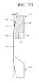
- FIG. 7Ais a cross-sectional view taken along line VII-VII of FIG. 6 , according to an embodiment of the present invention.
- FIG. 7Bis a cross-sectional view of a modification of FIG. 7A ;
- FIG. 8is a schematic view of the thin film deposition apparatus of FIG. 1 explaining a deposition process, according to an embodiment of the present invention
- FIG. 9illustrates a shadow zone of a thin layer deposited on a substrate when a deposition space is partitioned by first barrier walls and second barrier walls, as illustrated in FIG. 8 ;
- FIG. 10illustrates a shadow zone of a thin layer deposited on the substrate when the deposition space is not partitioned
- FIG. 11is a schematic view of a thin film deposition apparatus including a cooling member, according to an embodiment of the present invention.
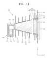
- FIG. 12is a schematic perspective view of a thin film deposition apparatus according to another embodiment of the present invention.
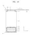
- FIG. 13is a schematic plan view of the thin film deposition apparatus of FIG. 12 , according to an embodiment of the present invention.
- FIG. 14is a schematic side view of the thin film deposition apparatus of FIG. 12 , according to an embodiment of the present invention.
- FIG. 15is a schematic perspective view of a thin film deposition apparatus according to another embodiment of the present invention.
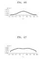
- FIG. 16is a graph schematically illustrating a distribution pattern of a deposition layer formed on a substrate when first slits are not tilted, in a thin film deposition apparatus according to an embodiment of the present invention.
- FIG. 17is a graph schematically illustrating a distribution pattern of a deposition layer formed on a substrate when first slits are tilted, in a thin film deposition apparatus according to an embodiment of the present invention.
- FIG. 1is a schematic perspective view of a thin film deposition apparatus 100 according to an embodiment of the present invention.
- FIG. 2is a schematic side view of the thin film deposition apparatus 100
- FIG. 3is a schematic plan view of the thin film deposition apparatus 100 .
- the thin film deposition apparatus 100includes a deposition source 110 , a first nozzle 120 , a first barrier wall assembly 130 , a second barrier wall assembly 140 , a second nozzle 150 , and a second nozzle frame 155 in order to deposit a deposition material 115 on a substrate 160 .
- the thin film deposition apparatus 100may include additional and/or different components, such as in the examples described below.
- the second barrier wall assembly 140includes a plurality of second barrier walls 141 and a second barrier wall frame 142 .
- all the components of the thin film deposition apparatus 100may be disposed within a chamber that is maintained at an appropriate degree of vacuum.
- the chamberis maintained at an appropriate vacuum in order to allow a deposition material to move in a substantially straight line through the thin film deposition apparatus 100 .
- the chamberIn order to deposit the deposition material 115 emitted from the deposition source 110 and discharged through the first nozzle 120 and the second nozzle 150 , on the substrate 160 in a desired pattern, the chamber should be maintained in a high-vacuum state as in a deposition method using a fine metal mask (FMM).
- the temperatures of the first barrier wall assembly 130 , the second barrier wall assembly 140 and the second nozzle 150should be sufficiently lower than the temperature of the deposition source 110 . In this regard, the temperatures of the first barrier wall assembly 130 , the second barrier wall assembly 140 and the second nozzle 150 may be about 100° C. or less.
- each of the first barrier wall assembly 130 and the second barrier wall assembly 140may include a cooling member such as a cooling pin.
- the substrate 160is a deposition target and is disposed in the chamber.
- the substrate 160may be a substrate for flat panel displays.
- a large substrate, such as a mother glass, for manufacturing a plurality of flat panel displays,may be used as the substrate 160 .
- Other substratesmay also be employed.
- the deposition source 110contains and heats the deposition material 115 .
- the deposition source 110is disposed in a side of the chamber which is opposite to the side in which the substrate 160 is disposed. As the deposition material 115 contained in the deposition source 110 is vaporized, the deposition material 115 is deposited on the substrate 160 .
- the deposition source 110includes a crucible 111 and a heater 115 .
- the crucible 111holds the deposition material 115 .
- the heater 112heats the crucible 111 to vaporize the deposition material 115 contained in the crucible 111 towards a side of the crucible 111 , and in particular, towards the first nozzle 120 .
- the first nozzle 120is disposed at a side of the deposition source 110 facing the substrate 160 .
- the first nozzle 120includes a plurality of first slits 121 that may be arranged at equal intervals in a Y-axis direction.
- the deposition material 115 that is vaporized in the deposition source 110passes through the first nozzle 120 towards the substrate 160 .
- the first barrier wall assembly 130is disposed at a side of the first nozzle 120 .
- the first barrier wall assembly 130includes a plurality of first barrier walls 131 , and a first barrier wall frame 132 that covers sides of the first barrier walls 131 .
- the plurality of first barrier walls 131may be arranged parallel to each other at equal intervals in the Y-axis direction.
- each of the first barrier walls 131may be formed to extend along an XZ plane in FIG. 1 , (i.e., perpendicular to the Y-axis direction).
- the plurality of first barrier walls 131 arranged as described abovepartition the space between the first nozzle 120 and the second nozzle 150 .
- the deposition spaceis divided by the first barrier walls 131 into sub-deposition spaces that respectively correspond to the first slits 121 through which the deposition material 115 is discharged.
- first barrier walls 131are respectively disposed between adjacent first slits 121 .
- Each of the first slits 121is disposed between two adjacent first barrier walls 131 .
- the first slits 121may be respectively located at the midpoint between two adjacent first barrier walls 131 , but the invention is not limited thereto.
- the deposition material 115 discharged through any one of the first slits 121is not mixed with deposition material 115 discharged through any other first slits 121 .
- the deposition material 115then passes through second slits 151 , which will be described later, so as to be deposited on the substrate 160 .
- the first barrier walls 131guide the deposition material 115 , which is discharged through the first slits 121 , so as not to flow in the Y-axis direction.
- the first barrier wall frame 132has upper and lower outer walls surrounding the first barrier walls 131 .
- the upper and lower outer wallsretain the positions of the first barrier walls 131 , and guide the deposition material 115 , which is discharged through the first slits 121 , so as not to flow in a Z-axis direction.
- the first barrier wall assembly 130may be constructed to be detachable from the thin film deposition apparatus 100 . To this end, the first barrier wall assembly 130 may be disposed to be separated from the first nozzle 120 as illustrated in FIG. 1 .
- a conventional FMM deposition methodhas low deposition efficiency.
- Deposition efficiencyrefers to the ratio of a deposition material deposited on a substrate to the deposition material vaporized from a deposition source.
- the conventional FMM deposition methodhas a deposition efficiency of about 32%. Furthermore, in the conventional FMM deposition method, about 68% of organic deposition material that is not deposited on the substrate remains adhered to a deposition apparatus, and thus reusing the deposition material is not easy.
- the deposition spaceis enclosed by the barrier wall assembly 130 , so that the deposition material 115 that remains undeposited is mostly deposited within the barrier wall assembly 130 .
- the first barrier wall assembly 130may be detached from the thin film deposition apparatus 100 and then placed in a separate deposition material recycling apparatus to recover the deposition material 115 . Due to the structure of the thin film deposition apparatus 100 , a reuse rate of the deposition material 115 is increased, so that the deposition efficiency is improved, thereby reducing the manufacturing costs.
- first barrier wall assembly 130may be spaced apart from the first nozzle 120 , heat transfer from the deposition source 110 to the first barrier wall assembly 130 is prevented. Thus, a temperature rise of the first barrier wall assembly 130 is suppressed. Furthermore, the separation of the first barrier wall assembly 130 from the first nozzle 120 provides a space that makes it easier to install a member (not shown) that blocks radiant heat from the first nozzle 120 . In particular, a space is provided for a member that blocks radiant heat from a surface of the first nozzle 120 close to the first slits 121 .
- the separation interval between the first barrier wall assembly 130 and the first nozzle 120may be set according to processing conditions, according to an aspect of the invention.
- the second barrier wall assembly 140is disposed at a side of the first barrier wall assembly 130 .
- the second barrier wall assembly 140includes a plurality of second barrier walls 141 , and a second barrier wall frame 142 that covers sides of the second barrier walls 141 .
- the plurality of second barrier walls 141may be arranged parallel to each other at equal intervals in the Y-axis direction as shown, but the invention is not limited thereto.
- each of the second barrier walls 141may be formed to extend along an XZ plane in FIG. 1 , (i.e., perpendicular to the Y-axis direction) but the invention s not limited thereto.
- the deposition spaceis divided by the first barrier walls 131 and second barrier walls 141 into sub-deposition spaces that respectively correspond to the first slits 121 through which the deposition material 115 is discharged.
- the second barrier wall frame 142may be formed in the shape of a window frame, but the invention is not limited thereto.
- the second barrier walls 141are arranged within the second barrier wall frame 142 .
- the second barrier wall frame 142supports the second barrier walls 141 , and guides the deposition material 115 , which is discharged through the first slits 121 and between the first barrier walls 131 , so as not to flow in the Z-axis direction.
- first barrier wall assembly 130the space between the first nozzle 120 and the second nozzle 150 is defined by the first barrier wall assembly 130 and the second barrier wall assembly 140
- aspects of the present inventionare not limited thereto.
- the space between the first nozzle 120 and the second nozzle 150may be defined only by the first barrier wall assembly 130 . That is, the second barrier wall assembly 140 may not be formed. However, if both the first and second barrier wall assemblies 130 and 140 are formed, the space between the first and second nozzles 120 and 150 may be partitioned more effectively than if only the first barrier wall assembly 130 is formed. Moreover, it is understood that additional barrier wall assemblies can be added.
- the second barrier walls 141is disposed to correspond to the first barrier walls 131 in one-to-one correspondence.
- the second barrier walls 141are respectively disposed to be parallel to and to be on the same plane as the first barrier walls 131 .
- Each pair of the corresponding first and second barrier walls 131 and 141are shown located on the same X-Z plane.
- the deposition material 115 discharged through any one of the first slits 121is not mixed with the deposition material 115 discharged through any other first slits 121 , and is deposited on the substrate 160 through the second slits 151 .
- the first barrier walls 131 and the second barrier walls 141guide the deposition material 115 , which is discharged through the first slits 121 , so as not to flow in the Y-axis direction.
- first barrier walls 131 and the second barrier walls 141are respectively illustrated as having the same thickness in the Y-axis direction, aspects of the present invention are not limited thereto.
- the second barrier walls 141which should be accurately aligned with the second nozzle 150 , may be formed to be relatively thin, whereas the first barrier walls 131 , which do not need to be precisely aligned with the second nozzle 150 , may be formed to be relatively thick. This makes it easier to manufacture the thin film deposition apparatus 100 .
- the second nozzle 150 and the second nozzle frame 155are disposed between the deposition source 110 and the substrate 160 . While not required, the shown second nozzle frame 155 is formed as a window frame having two approximately arched sides. The second nozzle 150 is bound inside the second nozzle frame 155 . The second nozzle 150 includes a plurality of second slits 151 that may be arranged at equal intervals in the Y-axis direction. The deposition material 115 that is vaporized in the deposition source 110 passes through the first nozzle 120 and the second nozzle 150 towards the substrate 160 . The second nozzle frame 155 will be described in detail later.
- the total number of second slits 151may be greater than the total number of first slits 121 .
- At least one first slit 121may be disposed between each two adjacent first barrier walls 131 .
- a plurality of second slits 151may be disposed between each two adjacent first barrier walls 131 .
- the space between the first nozzle 120 and the second nozzle 150is partitioned by the first barrier walls 131 into sub-deposition spaces that correspond to the first slits 121 , respectively.
- the deposition material 115 discharged from any one of the first slits 121passes through a plurality of second slits 151 disposed in the sub-deposition space corresponding to the first slit 121 , and is then deposited on the substrate 160 .
- second slits 151are shown in FIG. 3 as corresponding to each of the first slits 121 , aspects of the present invention are not limited thereto.
- the ratio of the number of second slits 151 to each first slit 121may vary according to the requirements of a product to be manufactured.
- the second nozzle 150may be manufactured by etching, which is the same method as used in a conventional method of manufacturing an FMM, and in particular, a striped FMM.
- the size of the FMMhas to be equal to the size of a substrate.
- the size of the FMMhas to be increased as the substrate becomes larger.
- a thin layeris deposited while the thin film deposition apparatus 100 is moved in the Z-axis direction within the chamber (not shown).
- the second nozzle 150may be significantly smaller than an FMM used in a conventional deposition method.
- the length of the second nozzle 150 in the Z-axis directionmay be less than the length of the substrate 160 in the Z-axis direction, provided that the width of the second nozzle 150 in the Y-axis direction is equal to the width of the substrate 160 in the Y-axis direction.
- the second nozzle 150may be formed to be significantly smaller than an FMM used in a conventional deposition method, it is relatively easy to manufacture the second nozzle 150 .
- the use of the second nozzle 150is smaller than an FMM used in a conventional deposition method and is more convenient in all processes. Examples of such processes include etching and subsequent other processes, such as precise extension, welding, moving, and cleaning processes.
- the deposition apparatus 100is more convenient and is more advantageous for a relatively large display device.
- FIG. 4is a schematic perspective view illustrating a binding structure of the second nozzle 150 and the second nozzle frame 155 , according to an embodiment of the present invention.
- the second nozzle 150is formed as a thin film and may be fixed to the thin film deposition apparatus 100 via the second nozzle frame 155 .
- the second nozzle frame 155may be formed in a lattice shape, which will be described in detail later, such as a window frame having two approximately arched sides.
- the second nozzle 150includes the plurality of second slits 151 and is bound inside the second nozzle frame 155 .
- the second nozzle 150is bound to the second nozzle frame 155 such that a tensile force is exerted on the second nozzle 150 by the second nozzle frame 155 .
- a degree of pattern precision of the second nozzle 150may be affected by a manufacturing error and a thermal expansion error during a deposition process of the second nozzle 150 .
- a counter force technique used to precisely extend an FMM and weld it to a framecan be used. This will now be described in detail below. Initially, as illustrated in FIG. 4 , an external tensile force is applied to the second nozzle 150 so that the second nozzle 150 is stretched outwards.
- a compression forceis applied to the second nozzle frame 155 in an opposite direction to the direction in which the external tensile force is applied to the second nozzle 150 , such that the compression force is in equilibrium with the external tensile force applied to the second nozzle 150 .
- the second nozzle 150is bound to the second nozzle frame 155 by, for example, welding edges of the second nozzle 150 to the second nozzle frame 155 .
- FIG. 4illustrates the second nozzle 150 and the second nozzle frame 155 bound to each other by welding points 152 .
- the second nozzle 150 and the second nozzle frame 155are relieved from all the external forces applied thereto to reach equilibrium, so that only a tensile force is exerted on the second nozzle 150 by the second nozzle frame 155 .
- the second nozzle 150may be manufactured with a manufacturing error of 2 ⁇ m or less.
- the temperature of the second nozzle frame 150may be maintained constant.
- the second nozzle 150which is disposed to face the deposition source 110 whose temperature is high, is always exposed to radiant heat from the deposition source 110 , so that the temperature of the second nozzle 150 is increased to some extent, for example, by about 5 to about 15° C.
- the second nozzle 150may expand, thus deteriorating a degree of pattern precision of the second nozzle 150 .
- the second nozzle 150is used. As shown, the second nozzle 150 is a stripe type nozzle, but the invention is not limited thereto.
- the second nozzle frame 155supports the second nozzle 150 such that a tensile force is exerted on the second nozzle 150 .
- the temperature of the second nozzle frame 155is maintained constant, thereby preventing pattern errors due to a temperature increase of the second nozzle 150 .
- the thermal expansion (pattern error) of the second nozzle 150 in a horizontal directionis affected by the temperature of the second frame nozzle 155 .
- the second nozzle 150thermally expands in a vertical direction (Z-axis direction).
- the vertical direction of the second nozzle 150is a scanning direction that is irrelevant to the degree of pattern precision of the second nozzle 150 .
- the second nozzle frame 155does not directly face the deposition source 110 in a vacuum condition, and thus is not exposed to the radiant heat from the deposition source 110 .
- the second nozzle frame 155is not connected to the deposition source 110 , there is no thermal conduction between the deposition source 110 and the second nozzle frame 155 .
- the temperature of the second nozzle frame 155is unlikely to rise. Even if the temperature of the second nozzle frame 155 rises slightly, for example, by 1 to 3° C., the temperature of the second nozzle frame 155 may be easily maintained constant, such as through the use of a thermal shield or a radiation fin.
- the thermal extension problem with the second nozzle 150no longer affects a problem of pattern precision of the second nozzle 150 .
- the degree of pattern precision of the second nozzle 150may be further improved.
- the second nozzle 150may be manufactured with a manufacturing error of 2 ⁇ m or less.
- an error in the pattern of the second nozzle 150 caused due to the thermal expansion of the second nozzle 150may be prevented by supporting the second nozzle 150 such that a tensile force is exerted thereon and by maintaining the temperature of the second nozzle frame 155 to be constant.
- the second nozzle 150may be manufactured with an error of less than 2 ⁇ m, which is attributed to a manufacturing error ( ⁇ 2) of the second nozzle 150 and a thermal expansion error ( ⁇ 0) of the second nozzle 150 .
- FIG. 5is a front view of the second nozzle frame 155 illustrated in FIG. 1 .
- FIG. 6is a perspective view of the second nozzle frame 155 illustrated in FIG. 1 .
- FIG. 7Ais a cross-sectional view taken along line VII-VII of FIG. 6 , according to an embodiment of the present invention.
- FIG. 6illustrates the second nozzle frame 155 viewed in a direction from the deposition source 110 illustrated in FIG. 1 .
- the second nozzle 150 illustrated in FIG. 1is not illustrated in FIGS. 5 and 6 but is illustrated in FIG. 7A .
- the second nozzle frame 155includes first frame portions 156 and second frame portions 157 .
- the second nozzle frame 155includes two first frame portions 156 extending in one direction (the Y direction) in parallel with each other.
- the second nozzle frame 155also includes two second frame portions 157 connecting the two first frame portions 156 to each other.
- the second portions 157are curved in one direction (the Y direction) so as to have an arched shape. That is, the second portions 157 form two convex sides of the second nozzle frame 155 .
- a compression forceis applied to the second nozzle frame 155 in an up/down direction (the Z direction) in order to bind the second nozzle frame 155 to the second nozzle 150 , and then is removed after the second nozzle frame 155 and the second nozzle 150 are bound to each other.
- the compression force during the binding processcorresponds to a tensile force applied to the second nozzle 150 after the bonding process is completed.
- the first frame portions 156 of the second nozzle frame 155sags in a direction in which the compression force is applied.
- the sagging of the first frame portions 156is similar to the sagging of beams in buildings.
- the second nozzle 150should be precisely aligned with the substrate 160 , which is a deposition target.
- precise binding between the second nozzle 150 and the second nozzle frame 155is important.
- the second nozzle frame 155 and the second nozzle 150may fail to be bound at a desired position and thus the second nozzle 150 may not be precisely aligned with the substrate 160 .
- the second frame portions 157 of the second nozzle frame 155are formed in an arched shape.
- the arched second frame portions 157have less resistance against a compression force than straight shaped second frame portions. That is, when the same compression force is applied, an arched structure contracts more than a straight structure.
- the second frame portions 157may buffer the compression force applied to the first frame portions 156 . That is, when the compression force is applied to the second nozzle frame 155 , the second frame portions 157 contract more than the first frame portions 156 by the compression force, and thus uneven deflection of the first frame portions 156 may be prevented.
- the second nozzle 150 and the second nozzle frame 155are combined at a desired position and thus precise alignment between the second nozzle 150 and the substrate 160 may not be disturbed.
- the thicknesses of center portions of the second frame portions 157are less than the thicknesses of both ends of the second frame portions 157 , i.e., parts connected to the first frame portions 156 . If the center portion of an arched structure is formed to be thinner than both ends thereof, the amount of deformation is reduced when a force is applied to the both ends. As such, due to the above-described structure of the second frame portions 157 , the deformation of the second nozzle frame 155 may be more effectively prevented.
- each of the first frame portions 156 of the second nozzle frame 155includes various surfaces such as a first surface 156 a , a second surface 156 b , a third surface 156 c , and a fourth surface 156 d .
- the first and second surfaces 156 a and 156 bare disposed at a front side of the second nozzle frame 155 , i.e., disposed to face the substrate 160
- the third and fourth surfaces 156 c and 156 dare disposed to face a direction opposite to the substrate 160 .
- the first and second surfaces 156 a and 156 bare adjacent to each other and the first surface 156 a is closer to the center of the second nozzle frame 155 than the second surface 156 b .
- the first surface 156 ais closer to the second slits 151 of the second nozzle 150 than the second surface 156 b .
- the first surface 156 ais flat and the second surface 156 b is sloping.
- the second nozzle 150 that is bound to the second nozzle frame 155may be flat in order to perform precise deposition on the substrate 160 , i.e., a deposition target. Since the second nozzle 150 is bound to the second nozzle frame 155 , the flatness of the second nozzle 150 is greatly influenced by the second nozzle frame 155 . In particular, the flatness on a center portion of the second nozzle 150 , in which the second slits 151 are formed, is important.
- the first surface 156 ais close to the second slits 151 and starts to contact the second nozzle 150 with reference to the second slits 151 .
- the flatness of the second nozzle 150may be easily ensured by forming the first surface 156 a , which is close to the second slits 151 and starts to contact the second nozzle 150 , to be flat.
- the second surface 156 bmay be curved, or gently curved. As such, an extension line S of the first surface 156 a does not coincide with the second surface 156 b .
- the welding points 152 for binding the second nozzle 150 to the second nozzle frame 155are formed on the second surface 156 b in order to prevent the welding points 152 from contacting a deposition target during deposition. Consequently, scratches on the substrate 160 are prevented.
- the welding points 152are formed on the second surface 156 b with a gap h from the extension line S of the first surface 156 a . The more the gap h is increased, the more easily scratches on the substrate 160 due to the welding points 152 may be prevented.
- the gap hmay be appropriately determined according to the conditions of a deposition process.
- the third surface 156 c of the second nozzle frame 155is disposed in a direction opposite to the direction toward the deposition target, (i.e., in a direction away from the second nozzle 150 ), and is formed to be flat.
- the second barrier wall frame 142is disposed at the rear side of the second nozzle frame 155 , (i.e., in the direction away from the second nozzle 150 ). In this case, the space of the thin film deposition apparatus 100 may be reduced by allowing the second barrier wall frame 142 of the second barrier wall assembly 140 to contact the third surface 156 c of the second nozzle frame 155 .
- the second barrier wall frame 142may easily contact the second nozzle frame 155 by forming the third surface 156 c to be flat and also forming a surface of the second barrier wall frame 142 , which corresponds to the third surface 156 c , to be flat.
- the fourth surface 156 d of the second nozzle frame 155connects the third surface 156 c to the first surface 156 a .
- the fourth surface 156 dis formed to have a slope. In this case, an obtuse angle is formed between the third and fourth surfaces 156 c and 156 d . That is, the fourth surface 156 d and an extension line of the third surface 156 c form a space M having a triangular shape.
- the space Mmay be occupied by the second barrier wall frame 142 or the second barrier walls 141 when the second barrier wall assembly 140 is disposed at the rear side of the second nozzle frame 155 .
- the placing of the second barrier wall assembly 140 at the rear side of the second nozzle frame 155is easy.
- the second nozzle frame 155may be modified to form a space for the second barrier walls 141 instead of the space M having a triangular shape.
- FIG. 7Billustrates a modification of FIG. 7A .
- the third surface 156 cis disposed in a direction opposite to a direction toward a deposition target, (i.e., in a direction away from the second nozzle 150 ), and is formed to be flat.
- the second barrier wall frame 142may easily contact the second nozzle frame 155 .
- the fourth surface 156 d of the second nozzle frame 155is disposed in a direction away from the second nozzle 150 , and is adjacent to the third surface 156 c .
- the fourth surface 156 dis formed to have a step with respect to the third surface 156 c and has a surface substantially parallel with the third surface 156 c .
- the fourth surface 156 dis closer to the second slits 151 of the second nozzle 150 than the third surface 156 c .
- the fourth surface 156 dmay be formed to be flat such that the fourth surface 156 d and an extension line of the third surface 156 c form a rectangular space M.
- the space Mmay be occupied by the second barrier wall frame 142 or the second barrier walls 141 when the second barrier wall assembly 140 is disposed at the rear side of the second nozzle frame 155 , and thus the second barrier wall assembly 140 may be easily disposed at the rear side of the second nozzle frame 155 .
- the first barrier wall assembly 130 and the second barrier wall assembly 140are disposed to be separated from each other by a predetermined distance.
- the first barrier wall assembly 130 and the second barrier wall assembly 140are separated from each other for the following reasons. However, it is understood that the assemblies 130 , 140 need not be separated in all aspects.
- the second barrier walls 141 and the second nozzle 150should be precisely aligned with each other, whereas it is unnecessary to precisely align the first barrier walls 131 and the second barrier walls 141 .
- high-precision controlmay be easily achieved by separating a part required to be precisely controlled from a part not required to be precisely controlled.
- the second barrier walls 141 and the second nozzle 150should be aligned with the substrate 160 to be accurate in position and to have a constant interval therebetween, and thus may require high-precision control.
- the second barrier wall assembly 140 and the second nozzle 150are separated from the deposition source 110 , the first nozzle 120 , and the first barrier wall assembly 130 .
- the deposition source 110 , the first nozzle 120 , and the first barrier wall assembly 130are relatively heavy parts not requiring precise control.
- the temperature of the first barrier wall assembly 130may increase to 100° C. or higher due to the high temperature of the deposition source 110 .
- the first barrier wall assembly 130 and the second barrier wall assembly 140are separated from each other.
- the second nozzle 150When the second nozzle 150 is separated from the chamber, it may be more straightforward to separate both the second nozzle 150 and the second barrier wall assembly 140 together than to separate only the second nozzle 150 . In order to make it more straightforward to separate the second nozzle 150 and the second barrier wall assembly 140 together from the chamber, the first barrier wall assembly 130 and the second barrier wall assembly 140 are separated from each other.
- the deposition material 115 adhered to the first barrier wall assembly 130is mostly reused, whereas the deposition material 115 adhered to the second barrier wall assembly 140 and the second nozzle 150 may not be reused.
- the first barrier wall assembly 130is separated from the second barrier wall assembly 140 and the second nozzle 150 , it may be straightforward to recover the deposition material 115 to be reused.
- a calibration plate(not shown) may be further installed in order to ensure uniformity of a thin layer over the entire substrate 160 .
- the first barrier wall assembly 130is separated from the second barrier wall assembly 140 , it is very easy to install the calibration plate.
- a partition(not shown) may be further installed in order to prevent deposition of the deposition material 115 on the second nozzle 150 after deposition onto the substrate 160 has been completed and before another substrate is subjected to deposition. This may extend a nozzle exchange cycle. It is straightforward to install the partition between the first barrier walls 131 and the second barrier walls 141 . Accordingly, the first barrier wall assembly 130 and the second barrier wall assembly 140 are separated from each other.
- FIG. 8is a schematic view illustrating deposition of the deposition material 115 in the thin film deposition apparatus 100 , according to an embodiment of the present invention.
- FIG. 9illustrates a shadow zone of a thin layer deposited on the substrate 160 when the deposition space is partitioned by the first barrier walls 131 and the second barrier walls 141 as illustrated in FIG. 8 .
- FIG. 10illustrates a shadow zone of a thin layer deposited on the substrate 160 when the deposition space is not partitioned.
- the deposition material 115 that is vaporized in the deposition source 110passes through the first nozzle 120 and the second nozzle 150 and is then deposited on the substrate 160 . Since the space between the first nozzle 120 and the second nozzle 150 is partitioned by the first barrier wall assembly 130 and the second barrier wall assembly 140 , the deposition material 115 discharged through any one of the first slits 121 of the first nozzle 120 is not mixed with the deposition material 115 discharged through any other adjacent first slits 121 due to the first barrier wall assembly 130 and the second barrier wall assembly 140 .
- an angle at which the deposition material 115 meets the second nozzle 150may be controlled by adjusting an interval d between each two adjacent first barrier walls 131 or each two adjacent second barrier walls 141 .
- the deposition material 115is deposited on the substrate 160 through the second nozzle 150 at an angle that is substantially perpendicular to the substrate 160 .
- the angle at which the deposition material 115 meets the second nozzle 150may be small.
- a width SH 1 of the shadow zone formed on the substrate 160is determined according to Equation 1.
- SH 1S*d s /h [Equation 1]
- Srepresents a distance between the second nozzle 150 and the substrate 160
- d srepresents a width of the first slits 121 adjacent to the deposition source 110
- hrepresents a distance between the deposition source 110 and the second nozzle 150 .
- the deposition material 115is discharged through the second nozzle 150 in a wider range of angles than in the case of FIG. 9 . This is because the deposition material 115 discharged not just through a first slit 121 directly facing a second slit 151 but also through first slits 121 other than the first slit 121 above, passes through the second slit 151 above and is then deposited on the substrate 160 .
- a width SH 2 of a shadow zone formed on the substrate 160is much greater than when the deposition space is partitioned by the first and second barrier walls 131 and 141 .
- the width SH 2 of the shadow zone formed on the substrate 160is determined using Equation 2.
- SH 2S* 2 n/h [Equation 2] where S denotes a distance between the second nozzle 150 and the substrate 160 , n denotes the interval between each two adjacent first slits 121 , and h denotes a distance between the deposition source 110 and the second nozzle 150 .
- d swhich is the width of the first slits 121
- nwhich is the interval between each two adjacent first slits 121 .
- the shadow zonemay have a smaller width when the space between the first nozzle 120 and the second nozzle 150 is partitioned by the first barrier wall assembly 130 and the second barrier wall assembly 140 .
- the width SH 2 of the shadow zone formed on the substrate 160may be reduced by any of the following: (1) by reducing the interval (“n”) between the adjacent first slits 121 , (2) by reducing the distance (“S”) between the second nozzle 150 and the substrate 160 , or (3) by increasing the distance (“h”) between the deposition source 110 and the second nozzle 150 .
- the shadow zone formed on the substrate 160may be reduced by installing the first barrier wall assembly 130 and the second barrier wall assembly 140 .
- the second nozzle 150can be separated from the substrate 160 .
- the second nozzle 150may be separated from the substrate 160 by a predetermined distance.
- depositionis performed with the FMM in close contact with a substrate in order to prevent formation of a shadow zone on the substrate.
- the contactmay cause defects.
- the second nozzle 150is disposed to be separated from the substrate 160 by a predetermined distance. This may be implemented by installing the first barrier wall assembly 130 and the second barrier wall assembly 140 to reduce the width of the shadow zone formed on the substrate 160 .
- a defect caused due to the contact between a substrate and a FMM, which occurs in a conventional deposition methodmay be prevented.
- the manufacturing speedsince it is unnecessary to use the FMM in close contact with the substrate during a deposition process, the manufacturing speed may be improved.
- FIG. 11is a schematic view of a thin film deposition apparatus including a cooling member, according to another embodiment of the present invention.
- each of the first barrier wall assembly 130 and the second barrier wall assembly 140may further include a cooling member.
- the temperatures of the first barrier wall assembly 130 and the second barrier wall assembly 140should be maintained to be considerably lower than the temperature of the deposition source 110 .
- each of the first barrier wall assembly 130 and the second barrier wall assembly 140may further include a cooling member.
- the first barrier wall assembly 132 and the second barrier wall assembly 142further include a first cooling fin 133 and a second cooling fin 143 , respectively.
- the first cooling fin 133is formed to protrude from an outer circumference of the first barrier wall frame 132 in order to radiatively cool the heat of the first barrier wall assembly 130 .
- the second cooling fin 143is formed to protrude from an outer surface of the second barrier wall frame 142 in order to radiatively cool the second barrier wall assembly 140 .
- a water-cooling methodmay be applied, whereby a pipe is installed in the first barrier wall assembly 130 and the second barrier wall assembly 140 , and a coolant flows through the pipe.
- the types of cooling membersare not limited to these examples.
- the second nozzle frame 155further includes a radiation fin 153 .
- a thermal shield 190is further disposed between the deposition source 110 and the second nozzle frame 155 .
- the second nozzle frame 155does not directly face the deposition source 110 in a vacuum condition, and thus is not exposed to the radiant heat from the deposition source 110 .
- the second nozzle frame 155is not connected to the deposition source 110 , there is no thermal conduction therebetween.
- the temperature of the second nozzle frame 155is unlikely to rise.
- the temperature of the second nozzle frame 155is still likely to rise slightly by about 1 to about 3° C.
- Such a temperature risemay be prevented via the radiation fin 153 , so that the temperature of the second nozzle frame 155 may be maintained constant.
- the radiation fin 153may be formed to protrude from an outer surface of the second nozzle frame 155 in order to radiatively cool the second nozzle frame 155 .
- the heat radiated from the deposition source 110 towards the second nozzle frame 155may be blocked by installing the thermal shield 190 between the deposition source 110 and the second nozzle frame 55 , so that the temperature of the second nozzle frame 155 may be maintained constant.
- FIG. 12is a schematic perspective view of a thin film deposition assembly 200 according to another embodiment of the present invention
- FIG. 13is a schematic sectional view of the thin film deposition assembly 200 illustrated in FIG. 12
- FIG. 14is a schematic plan view of the thin film deposition assembly 200 illustrated in FIG. 12 .
- the present embodiment illustrated in FIGS. 12 , 13 , and 14will now be described by focusing on differences between the previous embodiment and the present invention.
- the thin film deposition assembly 200includes a deposition source 210 , a first nozzle 220 , a second nozzle 250 , and a second nozzle frame 255 in order to deposit a deposition material 215 on a substrate 400 .
- the thin film deposition apparatus 200may include additional and/or different components, such as in the examples described below.
- all the components of the thin film deposition assembly 200may be disposed within a chamber that is maintained at an appropriate degree of vacuum.
- the chamberis maintained at an appropriate vacuum in order to allow a deposition material to move in a substantially straight line through the thin film deposition apparatus 200 .
- the chamberIn order to deposit the deposition material 215 emitted from the deposition source 210 and discharged through the first nozzle 220 and the second nozzle 250 , on the substrate 400 in a desired pattern, the chamber should be maintained in a high-vacuum state as in a deposition method using an FMM.
- the temperature of the second nozzle 250has to be sufficiently lower than the temperature of the deposition source 210 .
- the temperature of the second nozzle 250may be about 100° C. or less.
- the temperature of the second nozzle 250should be sufficiently low so as to reduce thermal expansion of the second nozzle 250 .
- the substrate 400which is a deposition target, is disposed in the chamber.
- the substrate 400may be a substrate for flat panel displays.
- a large substrate, such as a mother glass, for manufacturing a plurality of flat panel displays,may be used as the substrate 400 .
- Other substratesmay also be employed.
- the depositionmay be performed while the substrate 400 or the thin film deposition assembly 200 is moved relative to each other.
- depositionmay be continuously performed while the substrate 400 , which is disposed such as to face the thin film deposition assembly 200 , is moved in a Y-axis direction.
- depositionis performed in a scanning manner while the substrate 400 is moved in a direction of arrow A in FIG. 12 .
- the substrate 400is illustrated as being moved in the Y-axis direction in FIG. 12 when deposition is performed, aspects of the present invention are not limited thereto.
- Depositionmay be performed while the thin film deposition assembly 200 is moved in the Y-axis direction, whereas the substrate 400 is fixed.
- the second nozzle 250may be significantly smaller than an FMM used in a conventional deposition method.
- depositionis performed continuously, (i.e., in a scanning manner while the substrate 400 is moved in the Y-axis direction).
- lengths of the second nozzle 250 in the X-axis and Y-axis directionsmay be significantly less than the lengths of the substrate 400 in the X-axis and Y-axis directions.
- the second nozzle 250since the second nozzle 250 may be formed to be significantly smaller than an FMM used in a conventional deposition method, it is relatively easy to manufacture the second nozzle 250 .
- the use of the second nozzle 250which is smaller than an FMM used in a conventional deposition method, is more convenient in all processes, including etching and subsequent other processes, such as precise extension, welding, moving, and cleaning processes, compared to the conventional deposition method using the larger FMM. This is more advantageous for relatively large display devices.
- the thin film deposition apparatus 200 and the substrate 400may be separated from each other by a predetermined distance.
- the deposition source 210 that contains and heats the deposition material 215is disposed in an opposite side of the chamber to the side in which the substrate 400 is disposed.
- the deposition source 210includes a crucible 211 for holding the deposition material 215 , and a heater 212 for heating the crucible 211 .
- the first nozzle 220is disposed at a side of the deposition source 210 facing the substrate 400 .
- the first nozzle 220includes a plurality of first slits 221 that may be arranged at equal intervals in the Y-axis direction, i.e., in the scanning direction of the substrate 400 .
- the deposition material 215 that is vaporized in the deposition source 210passes through the first nozzle 220 towards the substrate 400 .
- a size of the pattern formed by the deposition material that is discharged through the second slits 221 of the second nozzle 250is only affected by the size of one first slit 221 , that is, it may be considered that only one first slit 221 exists in the X-axis direction, and thus there is no shadow zone on the substrate.
- the plurality of first slits 221are formed in the scanning direction of the substrate 400 , even when there is a difference between fluxes of the first slits 221 , the difference may be compensated and deposition uniformity may be maintained constantly.
- the second nozzle 250 and the second nozzle frame 255are disposed between the deposition source 210 and the substrate 400 .
- the second nozzle frame 255may be formed in a shape, similar to a window frame.
- the second nozzle 250is bound inside the second nozzle frame 255 .
- the second nozzle 250includes a plurality of second slits 251 arranged in the X-axis direction.
- the deposition material 215 that is vaporized in the deposition source 210passes through the first nozzle 220 and the second nozzle 250 towards the substrate 400 .
- the second nozzle 250may be manufactured by etching, which is the same method as used in a conventional method of manufacturing an FMM, and in particular, a striped FMM.
- the total number of second slits 251may be greater than the total number of first slits 221 .
- the second nozzle frame 255is formed in a shape such as a window frame having two approximately arched sides.
- the second nozzle frame 255includes first frame portions 256 and second frame portions 257 .
- the second nozzle frame 255includes two first frame portions 256 extending in one direction (X direction) in parallel with each other.
- the second nozzle frame 255also includes two second frame portions 257 each connecting the two first frame portions 256 to each other.
- the second frame portions 257are curved in another direction (X direction) so as to have arched shapes. In other words, the second frame portions 257 form two convex sides of the second nozzle frame 255 .
- the structure of the second nozzle frame 255 of the thin film deposition apparatus 200is the same as that illustrated in FIGS. 5 through 7B . Thus, a detailed description of the second nozzle frame 255 of the thin film deposition apparatus 200 will be omitted.
- a radiation fin as illustrated in FIG. 11may be formed on the second nozzle frame 255 .
- a thermal shieldmay be further disposed between the deposition source 210 and the second nozzle frame 255 .
- the deposition source 210 (and the first nozzle 220 coupled to the deposition source 210 ) and the second nozzle 250may be formed to be separated from each other by a predetermined distance, and the deposition source 210 (and the first nozzle 220 coupled to the deposition source 210 ) and the second nozzle 250 may be connected by a connection member 235 . That is, the deposition source 210 , the first nozzle 220 , and the second nozzle 250 may be formed integrally with each other by being connected to each other via the connection member 235 .
- the connection member 235may guide the deposition material 215 , which is discharged through the first slits 221 , to move straight, not to flow in the X-axis direction. In FIGS.
- connection members 235are formed on only left and right sides of the deposition source 210 , the first nozzle 220 , and the second nozzle 250 to guide the deposition material 215 not to flow in the X-axis direction, however, aspects of the present invention are not limited thereto. That is, the connection member 235 may be formed as a sealed type box to guide both flows of the deposition material 215 in the X-axis and Y-axis directions.
- the thin film deposition apparatus 200performs deposition while being moved relative to the substrate 400 .
- the second nozzle 250is separated from the substrate 400 by a predetermined distance.
- a conventional deposition method using an FMMdeposition is performed with the FMM in close contact with a substrate in order to prevent formation of a shadow zone on the substrate.
- the contactmay cause defects.
- the size of the maskhas to be the same as the size of the substrate since the mask cannot be moved relative to the substrate.
- the size of the maskhas to be increased as display devices become larger.
- the second nozzle 250is disposed to be separated from the substrate 400 by a predetermined distance.
- a maskis formed to be smaller than a substrate, and deposition is performed while the mask is moved relative to the substrate.
- the maskcan be easily manufactured.
- defects caused due to the contact between a substrate and a mask, which occurs in the conventional deposition methodmay be prevented.
- the manufacturing speedmay be improved.
- FIG. 15is a schematic perspective view of a thin film deposition apparatus 300 according to another embodiment of the present invention.
- the thin film deposition apparatus 300includes a deposition source 310 , a first nozzle 320 , a second nozzle 350 , and a second nozzle frame 355 in order to deposit a deposition material 315 on the substrate 400 .
- the thin film deposition apparatus 300may include additional and/or different components, such as in the examples described below.
- the deposition source 310includes a crucible 311 to hold the deposition material 315 , and a heater 312 to heat the crucible 311 .
- the first nozzle 320is disposed at a side of the deposition source 310 , and includes a plurality of first slits 321 arranged in the Y-axis direction.
- the second nozzle 350 and the second nozzle frame 355are further disposed between the deposition source 310 and the substrate 400 , and the second nozzle 350 includes a plurality of second slits 351 arranged in the X-axis direction.
- the deposition source 310 , the first nozzle 320 , and the second nozzle 350are connected to each other by a connection member 335 .
- the second nozzle 350is supported by the second nozzle frame 355 .
- the second nozzle frame 355is formed in a shape such as a window frame having two approximately arched sides.
- the second nozzle frame 355includes first frame portions 356 and second frame portions 357 .
- the second nozzle frame 355includes two first frame portions 356 extending in one direction (X direction) in parallel with each other.
- the second nozzle frame 355also includes two second frame portions 357 each connecting the two first frame portions 356 to each other.
- the second frame portions 357are curved in another direction (X direction) so as to have arched shapes. In other words, the second frame portions 357 form two convex sides of the second nozzle frame 355 .
- the structure of the second nozzle frame 355 of the thin film deposition apparatus 300is the same as that illustrated in FIGS. 5 through 7B . Thus, a detailed description of the second nozzle frame 355 of the thin film deposition apparatus 300 will be omitted.
- a radiation fin as illustrated in FIG. 11may be formed on the second nozzle frame 355 .
- a thermal shieldmay be further disposed between the deposition source 310 and the second nozzle frame 355 .
- the plurality of first slits 321 formed on the first nozzle 320are tilted at a predetermined angle.
- the first slits 321may include first slits 321 a and 321 b which are arranged in two rows, which are alternately arranged with each other. As shown, the first slits 321 a and 321 b are tilted at a predetermined angle on an X-Z plane.
- the first slits 321 a in a first roware tilted toward the first slits 321 b in a second row
- the first slits 321 b in the second roware tilted toward the first slits 321 a in the first row. That is, the first slits 321 a arranged in the left row are arranged to face a right end of the second nozzle 350
- the first slits 321 b arranged in the right roware arranged to face a left end of the second nozzle 350 .
- FIG. 16is a graph showing a distribution of a deposition layer formed on a substrate when first slits are not tilted in a thin film deposition apparatus according to an embodiment of the present invention
- FIG. 17is a graph showing a distribution of a deposition layer formed on a substrate when first slits are tilted in a thin film deposition apparatus according to an embodiment of the present invention. Comparing the graphs of FIGS. 16 and 17 with each other, a thickness of the deposition layer formed on both ends of the substrate when the first slits are tilted is relatively greater than a thickness of the deposition layer formed on both ends of the substrate when the first slits are not tilted, and thus, the uniformity of the deposition layer is improved.
- the deposition amount of the deposition materialmay be adjusted so that a difference between the thicknesses of the deposition layer at the center and ends of the substrate may be reduced and thus the entire thickness of the deposition layer may be constant, and moreover, the efficiency of utilizing the deposition material may be improved.
- a thin film deposition apparatusmay form a precise pattern on a large substrate.
Landscapes
- Chemical & Material Sciences (AREA)
- Chemical Kinetics & Catalysis (AREA)
- Engineering & Computer Science (AREA)
- Materials Engineering (AREA)
- Mechanical Engineering (AREA)
- Metallurgy (AREA)
- Organic Chemistry (AREA)
- Physical Vapour Deposition (AREA)
Abstract
Description
SH1=S*ds/h [Equation 1]
SH2=S*2n/h [Equation 2]
where S denotes a distance between the
Claims (47)
Applications Claiming Priority (4)
| Application Number | Priority Date | Filing Date | Title |
|---|---|---|---|
| KR10-2009-0050529 | 2009-06-08 | ||
| KR20090050529 | 2009-06-08 | ||
| KR20100010136AKR101193187B1 (en) | 2009-06-08 | 2010-02-03 | Apparatus for thin layer deposition |
| KR10-2010-0010136 | 2010-02-03 |
Publications (2)
| Publication Number | Publication Date |
|---|---|
| US20100310768A1 US20100310768A1 (en) | 2010-12-09 |
| US8882921B2true US8882921B2 (en) | 2014-11-11 |
Family
ID=43300946
Family Applications (1)
| Application Number | Title | Priority Date | Filing Date |
|---|---|---|---|
| US12/795,001Expired - Fee RelatedUS8882921B2 (en) | 2009-06-08 | 2010-06-07 | Thin film deposition apparatus |
Country Status (1)
| Country | Link |
|---|---|
| US (1) | US8882921B2 (en) |
Families Citing this family (29)
| Publication number | Priority date | Publication date | Assignee | Title |
|---|---|---|---|---|
| TWI475124B (en) | 2009-05-22 | 2015-03-01 | Samsung Display Co Ltd | Thin film deposition apparatus |
| JP5620146B2 (en) | 2009-05-22 | 2014-11-05 | 三星ディスプレイ株式會社Samsung Display Co.,Ltd. | Thin film deposition equipment |
| US8882920B2 (en) | 2009-06-05 | 2014-11-11 | Samsung Display Co., Ltd. | Thin film deposition apparatus |
| KR101117719B1 (en) | 2009-06-24 | 2012-03-08 | 삼성모바일디스플레이주식회사 | Apparatus for thin layer deposition |
| JP5328726B2 (en) | 2009-08-25 | 2013-10-30 | 三星ディスプレイ株式會社 | Thin film deposition apparatus and organic light emitting display device manufacturing method using the same |
| JP5677785B2 (en) | 2009-08-27 | 2015-02-25 | 三星ディスプレイ株式會社Samsung Display Co.,Ltd. | Thin film deposition apparatus and organic light emitting display device manufacturing method using the same |
| US8876975B2 (en) | 2009-10-19 | 2014-11-04 | Samsung Display Co., Ltd. | Thin film deposition apparatus |
| KR101146982B1 (en) | 2009-11-20 | 2012-05-22 | 삼성모바일디스플레이주식회사 | Aapparatus for thin layer deposition and method of manufacturing organic light emitting display apparatus |
| KR101084184B1 (en) | 2010-01-11 | 2011-11-17 | 삼성모바일디스플레이주식회사 | Thin film deposition apparatus |
| KR101174875B1 (en) | 2010-01-14 | 2012-08-17 | 삼성디스플레이 주식회사 | Apparatus for thin layer deposition, method for manufacturing of organic light emitting display apparatus using the same, and organic light emitting display apparatus manufactured by the method |
| KR101193186B1 (en)* | 2010-02-01 | 2012-10-19 | 삼성디스플레이 주식회사 | Apparatus for thin layer deposition, method for manufacturing of organic light emitting display apparatus using the same, and organic light emitting display apparatus manufactured by the method |
| KR101156441B1 (en) | 2010-03-11 | 2012-06-18 | 삼성모바일디스플레이주식회사 | Apparatus for thin layer deposition |
| KR101202348B1 (en) | 2010-04-06 | 2012-11-16 | 삼성디스플레이 주식회사 | Apparatus for thin layer deposition and method for manufacturing of organic light emitting display apparatus using the same |
| US8894458B2 (en) | 2010-04-28 | 2014-11-25 | Samsung Display Co., Ltd. | Thin film deposition apparatus, method of manufacturing organic light-emitting display device by using the apparatus, and organic light-emitting display device manufactured by using the method |
| KR101223723B1 (en) | 2010-07-07 | 2013-01-18 | 삼성디스플레이 주식회사 | Apparatus for thin layer deposition, method for manufacturing of organic light emitting display apparatus using the same, and organic light emitting display apparatus manufactured by the method |
| KR101673017B1 (en) | 2010-07-30 | 2016-11-07 | 삼성디스플레이 주식회사 | Apparatus for thin layer deposition and method for manufacturing of organic light emitting display apparatus using the same |
| KR101723506B1 (en) | 2010-10-22 | 2017-04-19 | 삼성디스플레이 주식회사 | Apparatus for organic layer deposition and method for manufacturing of organic light emitting display apparatus using the same |
| KR101738531B1 (en) | 2010-10-22 | 2017-05-23 | 삼성디스플레이 주식회사 | Method for manufacturing of organic light emitting display apparatus, and organic light emitting display apparatus manufactured by the method |
| KR20120045865A (en) | 2010-11-01 | 2012-05-09 | 삼성모바일디스플레이주식회사 | Apparatus for organic layer deposition |
| KR20120065789A (en) | 2010-12-13 | 2012-06-21 | 삼성모바일디스플레이주식회사 | Apparatus for organic layer deposition |
| KR101760897B1 (en) | 2011-01-12 | 2017-07-25 | 삼성디스플레이 주식회사 | Deposition source and apparatus for organic layer deposition having the same |
| KR101852517B1 (en) | 2011-05-25 | 2018-04-27 | 삼성디스플레이 주식회사 | Apparatus for organic layer deposition and method for manufacturing of organic light emitting display apparatus using the same |
| KR101840654B1 (en) | 2011-05-25 | 2018-03-22 | 삼성디스플레이 주식회사 | Apparatus for organic layer deposition and method for manufacturing of organic light emitting display apparatus using the same |
| KR101857249B1 (en) | 2011-05-27 | 2018-05-14 | 삼성디스플레이 주식회사 | Patterning slit sheet assembly, apparatus for organic layer deposition, method for manufacturing organic light emitting display apparatus and organic light emitting display apparatus |
| KR101826068B1 (en) | 2011-07-04 | 2018-02-07 | 삼성디스플레이 주식회사 | Apparatus for thin layer deposition |
| KR101959975B1 (en)* | 2012-07-10 | 2019-07-16 | 삼성디스플레이 주식회사 | Apparatus for organic layer deposition, method for manufacturing of organic light emitting display apparatus using the same, and organic light emitting display apparatus manufactured by the method |
| KR20140019579A (en)* | 2012-08-06 | 2014-02-17 | 삼성디스플레이 주식회사 | Evaporation apparatus |
| CN206396318U (en)* | 2017-01-24 | 2017-08-11 | 京东方科技集团股份有限公司 | A kind of crucible |
| CN108359944B (en)* | 2018-02-05 | 2019-10-29 | 信利光电股份有限公司 | A kind of coating apparatus, film plating process and the readable storage medium storing program for executing of curved surface cover board |
Citations (217)
| Publication number | Priority date | Publication date | Assignee | Title |
|---|---|---|---|---|
| JPS57194252U (en) | 1981-06-02 | 1982-12-09 | ||
| US4687939A (en) | 1983-11-07 | 1987-08-18 | Hitachi, Ltd. | Method and apparatus for forming film by ion beam |
| US4901667A (en) | 1985-08-09 | 1990-02-20 | Hitachi, Ltd. | Surface treatment apparatus |
| JPH04272170A (en) | 1991-02-25 | 1992-09-28 | Tokai Carbon Co Ltd | Graphite crucible for vacuum deposition |
| JPH05230628A (en) | 1992-02-18 | 1993-09-07 | Fujitsu Ltd | Metal film forming apparatus, metal material recovery method in metal film forming apparatus |
| JPH0827568B2 (en) | 1990-07-02 | 1996-03-21 | 三田工業株式会社 | Transfer paper separating device in image forming apparatus |
| JPH0995776A (en) | 1995-09-29 | 1997-04-08 | Sony Corp | Vacuum deposition device |
| US5742129A (en) | 1995-02-21 | 1998-04-21 | Pioneer Electronic Corporation | Organic electroluminescent display panel with projecting ramparts and method for manufacturing the same |
| WO1999025894A1 (en) | 1997-11-17 | 1999-05-27 | The Trustees Of Princeton University | Low pressure vapor phase deposition of organic thin films |
| JP2000068054A (en) | 1998-08-26 | 2000-03-03 | Hokuriku Electric Ind Co Ltd | Manufacture of el element |
| US6045671A (en) | 1994-10-18 | 2000-04-04 | Symyx Technologies, Inc. | Systems and methods for the combinatorial synthesis of novel materials |
| KR20000019254A (en) | 1998-09-08 | 2000-04-06 | 석창길 | Device for improving thin film thickness uniformity of cvd |
| KR20000023929A (en) | 1999-10-29 | 2000-05-06 | 최중호 | Apparatus and method for emitting odor |
| KR100257219B1 (en) | 1997-10-23 | 2000-05-15 | 박용관 | Method and device for making a safety operation of a polyethylene gas pipe valve arrangement |
| US6091195A (en) | 1997-02-03 | 2000-07-18 | The Trustees Of Princeton University | Displays having mesa pixel configuration |
| JP2001052862A (en) | 1999-08-04 | 2001-02-23 | Hokuriku Electric Ind Co Ltd | Manufacture of organic el element and device therefor |
| JP2001093667A (en) | 1999-09-28 | 2001-04-06 | Sanyo Electric Co Ltd | Organic light-emitting element, device and method for manufacturing the same |
| US20010006827A1 (en) | 1999-12-27 | 2001-07-05 | Semiconductor Energy Laboratory Co., Ltd. | Film formation apparatus and method for forming a film |
| KR20010059939A (en) | 1999-12-30 | 2001-07-06 | 송문섭 | Mobile station for mobile communication system |
| US6274198B1 (en) | 1997-02-24 | 2001-08-14 | Agere Systems Optoelectronics Guardian Corp. | Shadow mask deposition |
| US6280821B1 (en) | 1998-09-10 | 2001-08-28 | Ppg Industries Ohio, Inc. | Reusable mask and method for coating substrate |
| US20010019807A1 (en) | 1999-12-24 | 2001-09-06 | Tsutomu Yamada | Deposition mask and manufacturing method thereof, and electroluminescence display device and manufacturing method thereof |
| US20010026638A1 (en) | 2000-03-28 | 2001-10-04 | Katsuya Sangu | Positioning apparatus used in a process for producing multi-layered printed circuit board and method of using the same |
| KR20010092914A (en) | 2000-03-27 | 2001-10-27 | 윤종용 | Electrical static chuck comprising a shadow ring |
| KR200257218Y1 (en) | 2001-09-07 | 2001-12-24 | 엘지.필립스 엘시디 주식회사 | Mask apparatus for organic electro-luminescence device |
| KR20020000201A (en) | 2000-06-23 | 2002-01-05 | 최승락 | Method cleaning Liquid Chrystal Display using Laser and Vapor Phase |
| KR20020001555A (en) | 2000-06-22 | 2002-01-09 | 키도 준지 | Apparatus for and method of vacuum vapor deposition and organic electroluminescent device |
| JP2002075638A (en) | 2000-08-29 | 2002-03-15 | Nec Corp | Vapor deposition method of mask and vapor deposition device |
| US6371451B1 (en) | 1999-10-29 | 2002-04-16 | Korea Institute Of Science And Technology | Scent diffusion apparatus and method |
| US20020076847A1 (en) | 2000-09-28 | 2002-06-20 | Tsutomu Yamada | Method of attaching layer material and forming layer in predetermined pattern on substrate using mask |
| KR20020050922A (en) | 2000-12-22 | 2002-06-28 | 박종섭 | Virtual channel sdram |
| US20020168577A1 (en) | 2001-05-11 | 2002-11-14 | Jin-Mo Yoon | Method of crystallizing amorphous silicon |
| KR20020090934A (en) | 2002-08-27 | 2002-12-05 | 에이엔 에스 주식회사 | Organic material point source feeding unit in organic semiconductor device and method thereof |
| JP2003003250A (en) | 2001-06-22 | 2003-01-08 | Alps Electric Co Ltd | Vacuum deposition polymerization system and method for depositing organic film using the system |
| KR20030001745A (en) | 2001-06-27 | 2003-01-08 | 주식회사 하이닉스반도체 | Method for monitoring focus |
| JP2003077662A (en) | 2001-06-22 | 2003-03-14 | Junji Kido | Method and device for manufacturing organic electroluminescent element |
| KR20030034730A (en) | 2001-10-26 | 2003-05-09 | 삼성 엔이씨 모바일 디스플레이 주식회사 | Frame for mask of organic EL display devices |
| JP2003157973A (en) | 2001-09-05 | 2003-05-30 | Sony Corp | Manufacturing method and manufacturing apparatus of organic electroluminescence device, and manufacturing system and manufacturing method of display device using the same |
| US20030101932A1 (en) | 2001-12-05 | 2003-06-05 | Samsung Nec Mobile Display Co., Ltd. | Tension mask assembly for use in vacuum deposition of thin film of organic electroluminescent device |
| US20030101937A1 (en) | 2001-11-28 | 2003-06-05 | Eastman Kodak Company | Thermal physical vapor deposition source for making an organic light-emitting device |
| US6579422B1 (en) | 1999-07-07 | 2003-06-17 | Sony Corporation | Method and apparatus for manufacturing flexible organic EL display |
| US20030118950A1 (en) | 2000-08-07 | 2003-06-26 | Ching-Ian Chao | Method of manufacturing full-color organic electro-luminescent device |
| JP2003197531A (en) | 2001-12-21 | 2003-07-11 | Seiko Epson Corp | Patterning apparatus, patterning method, electronic element manufacturing method, circuit board manufacturing method, electronic device manufacturing method, electro-optical device and its manufacturing method, and electronic equipment |
| KR20030069684A (en) | 2002-02-22 | 2003-08-27 | 엘지.필립스 엘시디 주식회사 | Device for fixing mask and Ultraviolet irradiating device using the same |
| US20030168013A1 (en) | 2002-03-08 | 2003-09-11 | Eastman Kodak Company | Elongated thermal physical vapor deposition source with plural apertures for making an organic light-emitting device |
| JP2003297562A (en) | 2002-03-29 | 2003-10-17 | Sanyo Electric Co Ltd | Vapor deposition method |
| JP2003321767A (en) | 2002-04-26 | 2003-11-14 | Seiko Epson Corp | Method for depositing thin film, organic electroluminescence device, method for manufacturing organic electroluminescence device, and electronic equipment |
| KR20030091947A (en) | 2000-12-21 | 2003-12-03 | 아르코 케미컬 테크날러쥐. 엘.피. | Process for Producing Hydrogen Peroxide |
| US20030221620A1 (en) | 2002-06-03 | 2003-12-04 | Semiconductor Energy Laboratory Co., Ltd. | Vapor deposition device |
| US20030221614A1 (en) | 2002-06-03 | 2003-12-04 | Samsung Nec Mobile Display Co., Ltd., Ulsan-City, Republic Of Korea | Mask and mask frame assembly for evaporation |
| KR20030093959A (en) | 2002-06-03 | 2003-12-11 | 삼성 엔이씨 모바일 디스플레이 주식회사 | Mask frame assembly for thin layer vacuum evaporation of organic electro luminescence device |
| US20030232563A1 (en) | 2002-05-09 | 2003-12-18 | Isao Kamiyama | Method and apparatus for manufacturing organic electroluminescence device, and system and method for manufacturing display unit using organic electroluminescence devices |
| JP2004035964A (en) | 2002-07-04 | 2004-02-05 | Tokki Corp | Vapor deposition apparatus |
| JP2004043898A (en) | 2002-07-12 | 2004-02-12 | Canon Electronics Inc | Vapor deposition mask, and organic electroluminescence display device |
| US20040029028A1 (en) | 2002-08-05 | 2004-02-12 | Nec Plasma Display Coropration | Method for measuring gap between mask and substrate of display panel |
| JP2004076150A (en) | 2002-06-17 | 2004-03-11 | Sony Corp | Thin film forming system |
| US20040056244A1 (en) | 2002-09-23 | 2004-03-25 | Eastman Kodak Company | Device for depositing patterned layers in OLED displays |
| JP2004103269A (en) | 2002-09-05 | 2004-04-02 | Sanyo Electric Co Ltd | Manufacture method for organic electroluminescence display device |
| JP2004103341A (en) | 2002-09-09 | 2004-04-02 | Matsushita Electric Ind Co Ltd | Method for manufacturing organic electroluminescence device |
| EP1413644A2 (en) | 2002-10-24 | 2004-04-28 | Sony Corporation | Thin-film deposition device |
| KR20040034537A (en) | 2002-10-21 | 2004-04-28 | 도호꾸 파이오니어 가부시끼가이샤 | Vacuum evaporator |
| US20040086639A1 (en) | 2002-09-24 | 2004-05-06 | Grantham Daniel Harrison | Patterned thin-film deposition using collimating heated mask asembly |
| KR20040050045A (en) | 2002-12-03 | 2004-06-14 | 세이코 엡슨 가부시키가이샤 | Mask vapor deposition method, mask vapor deposition system, mask, process for manufacturing mask, apparatus for manufacturing display panel, display pane, and electronic device |
| US6749906B2 (en) | 2002-04-25 | 2004-06-15 | Eastman Kodak Company | Thermal physical vapor deposition apparatus with detachable vapor source(s) and method |
| US20040115342A1 (en) | 2002-11-22 | 2004-06-17 | Samsung Nec Mobile Display Co., Ltd. | Deposition mask frame assembly, method of fabricating the same, and method of fabricating organic electroluminescent device using the deposition mask frame assembly |
| US20040115338A1 (en)* | 2002-09-05 | 2004-06-17 | Sanyo Electric Co., Ltd. | Manufacturing method of organic electroluminescent display device |
| US20040127066A1 (en) | 2002-12-31 | 2004-07-01 | Yun-Ho Jung | Mask for sequential lateral solidification and crystallization method using thereof |
| JP2004199919A (en) | 2002-12-17 | 2004-07-15 | Tohoku Pioneer Corp | Method for manufacturing organic el display panel |
| US20040144321A1 (en) | 2003-01-28 | 2004-07-29 | Eastman Kodak Company | Method of designing a thermal physical vapor deposition system |
| US20040183435A1 (en) | 2003-03-19 | 2004-09-23 | Tohoku Pioneer Corporation | Film formation mask, organic EL panel, and method of manufacturing the organic EL panel |
| KR20040084747A (en) | 2003-03-27 | 2004-10-06 | 세이코 엡슨 가부시키가이샤 | Method of forming pattern, pattern forming apparatus, method of manufacturing device, conductive film wiring, electro-optical apparatus, and electronic equipment |
| US20040195530A1 (en) | 2003-04-04 | 2004-10-07 | Changsoo Kwak | Apparatus for measuring gap between mask and substrate using laser displacement sensor, and method thereof |
| US20040216673A1 (en) | 2003-02-14 | 2004-11-04 | Semiconductor Energy Laboratory Co., Ltd. | Manufacturing apparatus |
| JP2004349101A (en) | 2003-05-22 | 2004-12-09 | Seiko Epson Corp | Film forming method, film forming apparatus, method of manufacturing organic electroluminescent device, organic electroluminescent device |
| KR100463212B1 (en) | 2001-05-19 | 2004-12-23 | 주식회사 아이엠티 | Apparatus for dry surface-cleaning of materials |
| US20050016461A1 (en) | 2003-07-22 | 2005-01-27 | Eastman Kodak Company | Thermal physical vapor deposition source using pellets of organic material for making oled displays |
| JP2005044592A (en) | 2003-07-28 | 2005-02-17 | Toyota Industries Corp | Vapor deposition mask, film formation method using the vapor deposition mask, and film formation apparatus using the vapor deposition mask |
| US20050072361A1 (en)* | 2003-10-03 | 2005-04-07 | Yimou Yang | Multi-layered radiant thermal evaporator and method of use |
| US6878209B2 (en) | 1999-06-15 | 2005-04-12 | Toray Industries, Inc. | Organic electroluminescent device |
| JP2005122980A (en) | 2003-10-15 | 2005-05-12 | Chi Mei Electronics Corp | Image display device |
| US20050129489A1 (en) | 2003-11-12 | 2005-06-16 | Quan Yong C. | Load lock and load lock chamber using the same |
| JP2005165015A (en) | 2003-12-03 | 2005-06-23 | Seiko Epson Corp | Film forming mask, film forming apparatus, electro-optical device, and electronic apparatus |
| KR20050062853A (en) | 2003-12-19 | 2005-06-28 | 삼성전자주식회사 | Mask for forming the poly silicon layer and crystallization method of silicon using it |
| JP2005174843A (en) | 2003-12-15 | 2005-06-30 | Sony Corp | Deposition mask and its manufacturing method |
| US20050153472A1 (en) | 2003-12-26 | 2005-07-14 | Shinichi Yotsuya | Thin film formation method, thin film formation equipment, method of manufacturing organic electroluminescence device, organic electroluminescence device, and electronic apparatus |
| US20050166842A1 (en) | 2004-02-02 | 2005-08-04 | Fujitsu Limited | Vapor deposition mask and organic EL display device manufacturing method |
| JP2005235568A (en) | 2004-02-19 | 2005-09-02 | Seiko Epson Corp | Vapor deposition apparatus and organic EL device manufacturing method |
| US6946783B2 (en) | 2002-04-12 | 2005-09-20 | Lg Electronics Inc. | Shadow mask and flat display fabricated by using the same and method for fabricating the same |
| KR100520159B1 (en) | 2003-11-12 | 2005-10-10 | 삼성전자주식회사 | Apparatus and method for interference cancellation of ofdm system using multiple antenna |
| US20050229848A1 (en) | 2004-04-15 | 2005-10-20 | Asm Japan K.K. | Thin-film deposition apparatus |
| JP2005293968A (en) | 2004-03-31 | 2005-10-20 | Sanyo Electric Co Ltd | Manufacturing method of organic electroluminescent element |
| JP2005296737A (en) | 2004-04-07 | 2005-10-27 | Mikuni Corp | Beat plate |
| US20050263074A1 (en) | 2004-06-01 | 2005-12-01 | Tohoku Pioneer Corporation | Film formation source, vacuum film formation apparatus, organic EL panel and method of manufacturing the same |
| US20060011136A1 (en) | 2004-07-15 | 2006-01-19 | Semiconductor Energy Laboratory Co., Ltd. | Manufacturing apparatus |
| KR20060008602A (en) | 2004-07-21 | 2006-01-27 | 엘지전자 주식회사 | Organic Electroluminescent Layer Deposition Method |
| US20060022590A1 (en) | 2004-08-02 | 2006-02-02 | Xerox Corporation | OLEDs having inorganic material containing anode capping layer |
| US7006202B2 (en) | 2002-02-21 | 2006-02-28 | Lg.Philips Lcd Co., Ltd. | Mask holder for irradiating UV-rays |
| KR20060018745A (en) | 2004-08-25 | 2006-03-02 | 삼성에스디아이 주식회사 | Vertically Moved Organic Material Deposition Equipment |
| KR20060020050A (en) | 2004-08-30 | 2006-03-06 | 삼성에스디아이 주식회사 | High efficiency organic electroluminescent device and manufacturing method thereof |
| US20060090705A1 (en) | 2004-10-28 | 2006-05-04 | Kim Jae-Ho | Apparatus for fabricating display device |
| KR20060056706A (en) | 2004-11-22 | 2006-05-25 | 주식회사 하이닉스반도체 | Method of forming a semiconductor device |
| US20060110544A1 (en) | 2004-11-22 | 2006-05-25 | Kyekyoon Kim | Electrohydrodynamic spraying system |
| KR20060058459A (en) | 2004-11-25 | 2006-05-30 | 삼성에스디아이 주식회사 | Mask frame assembly, and method of manufacturing organic electroluminescent device using same |
| KR20060059068A (en) | 2004-11-26 | 2006-06-01 | 삼성에스디아이 주식회사 | Organic electroluminescent device and manufacturing method thereof |
| KR20060065978A (en) | 2004-12-11 | 2006-06-15 | 비오이 하이디스 테크놀로지 주식회사 | Slit mask |
| KR20060073367A (en) | 2004-12-24 | 2006-06-28 | 엘지전자 주식회사 | Organics Treatment Unit in Cleaning Room |
| JP2006172930A (en) | 2004-12-16 | 2006-06-29 | Hitachi High-Tech Electronics Engineering Co Ltd | Vacuum deposition method and EL display panel |
| JP2006176809A (en) | 2004-12-21 | 2006-07-06 | Ulvac Japan Ltd | Substrate and mask alignment method, organic thin film deposition method, and alignment apparatus |
| US20060144325A1 (en) | 2005-01-05 | 2006-07-06 | Samsung Sdi Co., Ltd. | Driving shaft of effusion cell for deposition system and deposition system having the same |
| KR20060080475A (en) | 2005-01-05 | 2006-07-10 | 삼성에스디아이 주식회사 | Drive shaft sealing device of deposition source for deposition system and deposition system having same |
| KR20060080482A (en) | 2005-01-05 | 2006-07-10 | 삼성에스디아이 주식회사 | Deposition source for material deposition and deposition apparatus having same |
| KR20060080481A (en) | 2005-01-05 | 2006-07-10 | 삼성에스디아이 주식회사 | Deposition source for material deposition and deposition system having same |
| US20060152641A1 (en) | 2005-01-10 | 2006-07-13 | Advantech Global, Ltd | Shadow mask deposition system for and method of forming a high resolution active matrix liquid crystal display (LCD) and pixel structures formed therewith |
| KR20060083510A (en) | 2005-01-17 | 2006-07-21 | 삼성전자주식회사 | Photomask Equipment Eliminates Defective By-Products |
| US20060174829A1 (en) | 2005-02-07 | 2006-08-10 | Semes Co., Ltd. | Apparatus for processing substrate |
| JP2006210038A (en) | 2005-01-26 | 2006-08-10 | Seiko Epson Corp | Mask manufacturing method |
| KR20060092387A (en) | 2005-02-17 | 2006-08-23 | 비오이 하이디스 테크놀로지 주식회사 | Multi Slit Mask |
| US20060205101A1 (en) | 2004-12-03 | 2006-09-14 | Lee Jae-Ho | Laser irradiation device, patterning method and method of fabricating organic light emitting display (OLED) using the patterning method |
| KR20060098755A (en) | 2005-03-07 | 2006-09-19 | 에스케이씨 주식회사 | Vacuum deposition apparatus and method of organic light emitting diode |
| KR20060104675A (en) | 2005-03-31 | 2006-10-09 | 세메스 주식회사 | Substrate processing equipment |
| KR20060104677A (en) | 2005-03-31 | 2006-10-09 | 세메스 주식회사 | Substrate transfer device and device for depositing organic thin film on substrate |
| KR20060104288A (en) | 2005-03-30 | 2006-10-09 | 엘지전자 주식회사 | Clamping apparatus and method of mask for organic light emitting display device |
| JP2006275433A (en) | 2005-03-29 | 2006-10-12 | National Institute Of Advanced Industrial & Technology | Absorption type cooling and refrigeration equipment |
| KR100635903B1 (en) | 2004-01-29 | 2006-10-18 | 미쯔비시 히다찌 세이떼쯔 기까이 가부시끼가이샤 | Vacuum evaporator |
| KR20060109627A (en) | 2005-04-18 | 2006-10-23 | 엘지전자 주식회사 | Organic electroluminescent layer forming mask |
| JP2006292955A (en) | 2005-04-08 | 2006-10-26 | V Technology Co Ltd | Scan exposure method and scan exposure apparatus |
| KR20060114462A (en) | 2005-04-29 | 2006-11-07 | 엘지전자 주식회사 | Clamping apparatus and method of mask for organic light emitting display device |
| KR20060123944A (en) | 2005-05-30 | 2006-12-05 | 삼성에스디아이 주식회사 | Alignment device and alignment method of substrate and mask |
| US20060272572A1 (en) | 2005-06-06 | 2006-12-07 | Sumitomo Electric Industries, Ltd. | Nitride semiconductor substrate and method of producing same |
| US20070022955A1 (en) | 2005-07-28 | 2007-02-01 | Marcus Bender | Vapor deposition device |
| JP2007047293A (en) | 2005-08-08 | 2007-02-22 | Casio Comput Co Ltd | Musical sound generator and program |
| KR100687007B1 (en) | 2005-03-22 | 2007-02-26 | 세메스 주식회사 | Organic thin film deposition apparatus used for manufacturing organic electroluminescent device |
| US20070054044A1 (en) | 2003-07-10 | 2007-03-08 | Sumitomo Titanium | Method for forming metal oxide coating film and vapor deposition apparatus |
| KR20070025164A (en) | 2005-08-31 | 2007-03-08 | 삼성에스디아이 주식회사 | Organic vapor deposition source and heating source control method thereof |
| KR100696547B1 (en) | 2005-12-09 | 2007-03-19 | 삼성에스디아이 주식회사 | Deposition method |
| KR100696550B1 (en) | 2005-12-09 | 2007-03-19 | 삼성에스디아이 주식회사 | Deposition equipment |
| KR100697663B1 (en) | 2005-10-27 | 2007-03-20 | 세메스 주식회사 | Organic material deposition apparatus |
| KR100698033B1 (en) | 2000-12-29 | 2007-03-23 | 엘지.필립스 엘시디 주식회사 | Organic electroluminescent device and manufacturing method thereof |
| KR20070035796A (en) | 2005-09-28 | 2007-04-02 | 엘지전자 주식회사 | Device for manufacturing organic electroluminescent display device |
| KR20070050793A (en) | 2006-08-28 | 2007-05-16 | 주식회사 대우일렉트로닉스 | Micro heater and crucible manufacturing method, and organic vacuum deposition apparatus provided with them |
| KR100723627B1 (en) | 2006-08-01 | 2007-06-04 | 세메스 주식회사 | The evaporation source of the organic thin film deposition apparatus |
| KR100726132B1 (en) | 2000-10-31 | 2007-06-12 | 엘지.필립스 엘시디 주식회사 | Array substrate for liquid crystal display device and manufacturing method |
| US20070148337A1 (en) | 2005-12-22 | 2007-06-28 | Nichols Jonathan A | Flame-perforated aperture masks |
| KR100739309B1 (en) | 2006-10-13 | 2007-07-12 | 삼성에스디아이 주식회사 | Thin film deposition mask and organic electroluminescent display device using the same |
| US20070157879A1 (en) | 2006-01-11 | 2007-07-12 | Seiko Epson Corporation | Mask, film forming method, light-emitting device, and electronic apparatus |
| US20070163497A1 (en) | 2006-01-17 | 2007-07-19 | Eastman Kodak Company | Two-dimensional aperture array for vapor deposition |
| KR20070078713A (en) | 2006-01-27 | 2007-08-01 | 캐논 가부시끼가이샤 | Deposition apparatus and deposition method of organic compound |
| KR20070080635A (en) | 2006-02-08 | 2007-08-13 | 주식회사 아바코 | Organic Evaporation Boat |
| US20070231460A1 (en) | 2006-03-31 | 2007-10-04 | Canon Kabushiki Kaisha | Film formation method |
| KR20070101842A (en) | 2004-09-08 | 2007-10-17 | 도레이 가부시끼가이샤 | Organic electroluminescent device and manufacturing method thereof |
| KR100768212B1 (en) | 2006-03-28 | 2007-10-18 | 삼성에스디아이 주식회사 | Thin film deposition method and manufacturing method of organic light emitting display device |
| KR100770653B1 (en) | 2006-05-25 | 2007-10-29 | 에이엔 에스 주식회사 | Thin film deposition equipment |
| KR20070105595A (en) | 2006-04-27 | 2007-10-31 | 두산메카텍 주식회사 | Organic thin film deposition apparatus |
| KR20070112668A (en) | 2006-05-22 | 2007-11-27 | 세메스 주식회사 | Linear Evaporator for Fabrication of Organic Thin Film |
| KR100787457B1 (en) | 2006-08-31 | 2007-12-26 | 삼성에스디아이 주식회사 | Substrate alignment device and manufacturing apparatus for organic light emitting display device including the same |
| KR20080001184A (en) | 2006-06-29 | 2008-01-03 | 엘지.필립스 엘시디 주식회사 | Deposition Stem of Organic Electroluminescent Device and Manufacturing Method of Organic Electroluminescent Device Using Same |
| WO2008004792A1 (en) | 2006-07-03 | 2008-01-10 | Yas Co., Ltd. | Multiple nozzle evaporator for vacuum thermal evaporation |
| US20080018236A1 (en) | 2004-09-08 | 2008-01-24 | Toray Industries, Inc. | Organic Electroluminescent Device and Manufacturing Method Thereof |
| KR100797787B1 (en) | 2005-06-03 | 2008-01-24 | 주식회사 아이엠티 | Dry cleaning system using laser |
| KR100800125B1 (en) | 2006-06-30 | 2008-01-31 | 세메스 주식회사 | Source Shutter and Substrate Control Method of Organic Light-Emitting Device Deposition Equipment |
| KR100823508B1 (en) | 2006-10-19 | 2008-04-21 | 삼성에스디아이 주식회사 | Evaporation source and deposition apparatus having same |
| KR20080036983A (en) | 2005-08-25 | 2008-04-29 | 히다치 조센 가부시키가이샤 | Alignment device for vacuum deposition |
| US20080100201A1 (en) | 2006-10-31 | 2008-05-01 | Chunghwa Picture Tubes, Ltd. | Organic electroluminescence device and fabricating method thereof |
| JP2008108628A (en) | 2006-10-26 | 2008-05-08 | Kyocera Corp | Organic EL display and manufacturing method thereof |
| KR20080044775A (en) | 2006-11-16 | 2008-05-21 | 자이단호징 야마가타켄산교기쥬츠신코기코 | Evaporation source and vacuum deposition apparatus using the same |
| KR20080048653A (en) | 2006-11-29 | 2008-06-03 | 엘지디스플레이 주식회사 | Mask device and manufacturing method of flat panel display device using same |
| US20080131587A1 (en) | 2006-11-30 | 2008-06-05 | Boroson Michael L | Depositing organic material onto an oled substrate |
| US20080145521A1 (en) | 2006-12-13 | 2008-06-19 | Guo G X | System and process for fabricating photovoltaic cell |
| JP2008521165A (en) | 2004-11-16 | 2008-06-19 | インターナショナル・ビジネス・マシーンズ・コーポレーション | Organic light emitting device, method for manufacturing the same, and array comprising a plurality of organic light emitting devices |
| KR100839380B1 (en) | 2006-10-30 | 2008-06-19 | 삼성에스디아이 주식회사 | Vacuum deposition apparatus of organic light emitting display |
| KR20080055124A (en) | 2006-12-14 | 2008-06-19 | 엘지디스플레이 주식회사 | Deposition equipment |
| KR20080060400A (en) | 2006-12-27 | 2008-07-02 | 엘지디스플레이 주식회사 | Manufacturing method of array substrate and manufacturing method of organic light generating device using same |
| KR20080061132A (en) | 2006-12-28 | 2008-07-02 | 엘지디스플레이 주식회사 | Organic film deposition apparatus |
| KR20080062212A (en) | 2006-12-29 | 2008-07-03 | 세메스 주식회사 | Organic thin film deposition apparatus |
| KR20080061666A (en) | 2006-12-28 | 2008-07-03 | 세메스 주식회사 | Organic thin film deposition apparatus |
| KR20080061774A (en) | 2006-12-28 | 2008-07-03 | 엘지전자 주식회사 | Apparatus and method for aligning mask of liquid crystal display |
| KR20080003720U (en) | 2007-03-02 | 2008-09-05 | 동양매직 주식회사 | Integrated bidet gas leak and overpressure valve |
| US20080216741A1 (en) | 2001-10-26 | 2008-09-11 | Hermosa Thin Film Co., Ltd. | Dynamic film thickness control system/method and its utilization |
| US20080238294A1 (en) | 2007-03-30 | 2008-10-02 | The Penn State Research Foundation | Mist fabrication of quantum dot devices |
| KR20080109559A (en) | 2007-06-13 | 2008-12-17 | 주식회사 하이닉스반도체 | Masks and manufacturing methods for providing local modified illumination |
| US20090017192A1 (en) | 2007-07-12 | 2009-01-15 | Hiroyasu Matsuura | Vapor deposition method and apparatus |
| JP2009024208A (en) | 2007-07-18 | 2009-02-05 | Fujifilm Corp | Vapor deposition apparatus, vapor deposition method, and electronic device and organic electroluminescence device having layers patterned using the method |
| JP2009081165A (en) | 2007-09-25 | 2009-04-16 | Yamaha Motor Co Ltd | Substrate processing apparatus, surface mounting machine, printing machine, inspection machine, and coating machine |
| KR20090038733A (en) | 2007-10-16 | 2009-04-21 | 주식회사 실트론 | Heat treatment method for improving surface roughness of SOI wafer and heat treatment apparatus therefor |
| JP2009087910A (en) | 2007-09-10 | 2009-04-23 | Ulvac Japan Ltd | Vapor deposition apparatus and film formation method |
| KR20090040618A (en) | 2007-10-22 | 2009-04-27 | 네오뷰코오롱 주식회사 | Deposition mask unit |
| KR20090052155A (en) | 2007-11-20 | 2009-05-25 | 엘지디스플레이 주식회사 | OLED display device |
| KR20090053417A (en) | 2007-11-23 | 2009-05-27 | 삼성모바일디스플레이주식회사 | Mask assembly for thin film deposition of flat panel display |
| KR20090066996A (en) | 2007-12-20 | 2009-06-24 | 다이나믹솔라디자인 주식회사 | Continuous substrate processing system |
| KR20090093161A (en) | 2008-02-28 | 2009-09-02 | 삼성모바일디스플레이주식회사 | Evaporating apparatus and method for forming thin film |
| KR20090097453A (en) | 2008-03-11 | 2009-09-16 | 삼성모바일디스플레이주식회사 | Thin film formation method |
| US20090229524A1 (en) | 2006-07-03 | 2009-09-17 | Yas Co., Ltd. | Multiple Nozzle Evaporator for Vacuum Thermal Evaporation |
| US20090277386A1 (en) | 2006-04-13 | 2009-11-12 | Ulvac, Inc. | Catalytic chemical vapor deposition apparatus |
| KR20100000129U (en) | 2008-06-26 | 2010-01-06 | (주) 씨앤앤 | Luminous watermark |
| KR20100000128A (en) | 2008-06-24 | 2010-01-06 | 엘지디스플레이 주식회사 | A deposition mask unit for fabrication of organic light emitting display device |
| US20100055810A1 (en) | 2008-09-01 | 2010-03-04 | Samsung Mobile Display Co.,Ltd. | Mask for thin film deposition and method of manufacturing oled using the same |
| KR20100047796A (en) | 2008-10-29 | 2010-05-10 | 소니 주식회사 | Organic el display and method of manufacturing the same |
| US20100196607A1 (en) | 2007-06-19 | 2010-08-05 | 3M Innovative Properties Company | Systems and methods for fabricating displacement scales |
| US20100192856A1 (en) | 2009-02-05 | 2010-08-05 | Dong-Young Sung | Mask assembly and deposition and apparatus for a flat panel display using the same |
| KR20100099806A (en) | 2009-03-04 | 2010-09-15 | 삼성전자주식회사 | Holographic exposure apparatus |
| US20100271602A1 (en)* | 2009-04-28 | 2010-10-28 | Noritsugu Hanazaki | Protective apparatus, mask, mask forming apparatus, mask forming method, exposure apparatus, device fabricating method, and foreign matter detecting apparatus |
| JP2010261081A (en) | 2009-05-08 | 2010-11-18 | V Technology Co Ltd | Vapor deposition method and vapor deposition apparatus |
| US20100297349A1 (en) | 2009-05-22 | 2010-11-25 | Samsung Mobile Display Co., Ltd. | Thin film deposition apparatus |
| US20100297348A1 (en) | 2009-05-22 | 2010-11-25 | Samsung Mobile Display Co., Ltd | Thin film deposition apparatus |
| KR20100126125A (en) | 2009-05-22 | 2010-12-01 | 삼성모바일디스플레이주식회사 | Thin film deposition apparatus |
| US20100330265A1 (en) | 2009-06-24 | 2010-12-30 | Samsung Mobile Display Co., Ltd. | Thin film deposition apparatus |
| US20100330712A1 (en) | 2009-06-25 | 2010-12-30 | Samsung Mobile Display Co., Ltd. | Thin film deposition apparatus and method of manufacturing organic light emitting device by using the same |
| US20110033621A1 (en) | 2009-08-10 | 2011-02-10 | Samsung Mobile Display Co., Ltd. | Thin film deposition apparatus including deposition blade |
| US20110033619A1 (en) | 2009-08-10 | 2011-02-10 | Samsung Mobile Display Co., Ltd. | Thin film deposition apparatus including deposition blade |
| US20110048320A1 (en) | 2009-09-01 | 2011-03-03 | Samsung Mobile Display Co., Ltd. | Thin film deposition apparatus |
| US20110052791A1 (en) | 2009-08-27 | 2011-03-03 | Samsung Mobile Display Co., Ltd. | Thin film deposition apparatus and method of manufacturing organic light-emitting display apparatus using the same |
| US20110052795A1 (en) | 2009-09-01 | 2011-03-03 | Samsung Mobile Display Co., Ltd. | Thin film deposition apparatus and method of manufacturing organic light-emitting display device by using the same |
| US20110053296A1 (en) | 2009-08-25 | 2011-03-03 | Samsung Mobile Display Co., Ltd. | Thin film deposition apparatus and method of manufacturing organic light-emitting display device by using the same |
| US20110220019A1 (en) | 2010-03-09 | 2011-09-15 | Lee Choong-Ho | Mask frame assembly for thin film deposition and method of assembling the same |
| US20120009328A1 (en) | 2010-07-12 | 2012-01-12 | Jae-Kwang Ryu | Thin film deposition apparatus and method of manufacturing organic light-emitting display device by using the same |
| US8193011B2 (en) | 2009-08-24 | 2012-06-05 | Samsung Mobile Display Co., Ltd. | Thin film deposition apparatus and method of manufacturing organic light-emitting display device by using the same |
| US20120313251A1 (en) | 2011-06-10 | 2012-12-13 | Toshiba America Electronic Components, Inc. | Interconnect structure with improved alignment for semiconductor devices |
- 2010
- 2010-06-07USUS12/795,001patent/US8882921B2/ennot_activeExpired - Fee Related
Patent Citations (264)
| Publication number | Priority date | Publication date | Assignee | Title |
|---|---|---|---|---|
| JPS57194252U (en) | 1981-06-02 | 1982-12-09 | ||
| US4687939A (en) | 1983-11-07 | 1987-08-18 | Hitachi, Ltd. | Method and apparatus for forming film by ion beam |
| US4901667A (en) | 1985-08-09 | 1990-02-20 | Hitachi, Ltd. | Surface treatment apparatus |
| JPH0827568B2 (en) | 1990-07-02 | 1996-03-21 | 三田工業株式会社 | Transfer paper separating device in image forming apparatus |
| JPH04272170A (en) | 1991-02-25 | 1992-09-28 | Tokai Carbon Co Ltd | Graphite crucible for vacuum deposition |
| JPH05230628A (en) | 1992-02-18 | 1993-09-07 | Fujitsu Ltd | Metal film forming apparatus, metal material recovery method in metal film forming apparatus |
| US6045671A (en) | 1994-10-18 | 2000-04-04 | Symyx Technologies, Inc. | Systems and methods for the combinatorial synthesis of novel materials |
| US5742129A (en) | 1995-02-21 | 1998-04-21 | Pioneer Electronic Corporation | Organic electroluminescent display panel with projecting ramparts and method for manufacturing the same |
| JPH0995776A (en) | 1995-09-29 | 1997-04-08 | Sony Corp | Vacuum deposition device |
| US6091195A (en) | 1997-02-03 | 2000-07-18 | The Trustees Of Princeton University | Displays having mesa pixel configuration |
| US6274198B1 (en) | 1997-02-24 | 2001-08-14 | Agere Systems Optoelectronics Guardian Corp. | Shadow mask deposition |
| KR100257219B1 (en) | 1997-10-23 | 2000-05-15 | 박용관 | Method and device for making a safety operation of a polyethylene gas pipe valve arrangement |
| WO1999025894A1 (en) | 1997-11-17 | 1999-05-27 | The Trustees Of Princeton University | Low pressure vapor phase deposition of organic thin films |
| JP2000068054A (en) | 1998-08-26 | 2000-03-03 | Hokuriku Electric Ind Co Ltd | Manufacture of el element |
| KR20000019254A (en) | 1998-09-08 | 2000-04-06 | 석창길 | Device for improving thin film thickness uniformity of cvd |
| US6280821B1 (en) | 1998-09-10 | 2001-08-28 | Ppg Industries Ohio, Inc. | Reusable mask and method for coating substrate |
| US6878209B2 (en) | 1999-06-15 | 2005-04-12 | Toray Industries, Inc. | Organic electroluminescent device |
| US6579422B1 (en) | 1999-07-07 | 2003-06-17 | Sony Corporation | Method and apparatus for manufacturing flexible organic EL display |
| JP2001052862A (en) | 1999-08-04 | 2001-02-23 | Hokuriku Electric Ind Co Ltd | Manufacture of organic el element and device therefor |
| JP2001093667A (en) | 1999-09-28 | 2001-04-06 | Sanyo Electric Co Ltd | Organic light-emitting element, device and method for manufacturing the same |
| KR20000023929A (en) | 1999-10-29 | 2000-05-06 | 최중호 | Apparatus and method for emitting odor |
| US6371451B1 (en) | 1999-10-29 | 2002-04-16 | Korea Institute Of Science And Technology | Scent diffusion apparatus and method |
| US20010019807A1 (en) | 1999-12-24 | 2001-09-06 | Tsutomu Yamada | Deposition mask and manufacturing method thereof, and electroluminescence display device and manufacturing method thereof |
| KR100827760B1 (en) | 1999-12-27 | 2008-05-07 | 가부시키가이샤 한도오따이 에네루기 켄큐쇼 | Method of manufacturing an electroluminescence display device |
| US20010006827A1 (en) | 1999-12-27 | 2001-07-05 | Semiconductor Energy Laboratory Co., Ltd. | Film formation apparatus and method for forming a film |
| KR20010059939A (en) | 1999-12-30 | 2001-07-06 | 송문섭 | Mobile station for mobile communication system |
| KR20010092914A (en) | 2000-03-27 | 2001-10-27 | 윤종용 | Electrical static chuck comprising a shadow ring |
| KR20010093666A (en) | 2000-03-28 | 2001-10-29 | 미즈따니군지 | Positioning apparatus used in a process for producing multi-layered printed circuit board and method of using the same |
| US20010026638A1 (en) | 2000-03-28 | 2001-10-04 | Katsuya Sangu | Positioning apparatus used in a process for producing multi-layered printed circuit board and method of using the same |
| KR20020001555A (en) | 2000-06-22 | 2002-01-09 | 키도 준지 | Apparatus for and method of vacuum vapor deposition and organic electroluminescent device |
| US20020017245A1 (en) | 2000-06-22 | 2002-02-14 | Matsushita Electric Works, Ltd. | Apparatus for and method of vacuum vapor deposition and organic electroluminescent device |
| KR20020000201A (en) | 2000-06-23 | 2002-01-05 | 최승락 | Method cleaning Liquid Chrystal Display using Laser and Vapor Phase |
| US20030118950A1 (en) | 2000-08-07 | 2003-06-26 | Ching-Ian Chao | Method of manufacturing full-color organic electro-luminescent device |
| JP2002075638A (en) | 2000-08-29 | 2002-03-15 | Nec Corp | Vapor deposition method of mask and vapor deposition device |
| US20020076847A1 (en) | 2000-09-28 | 2002-06-20 | Tsutomu Yamada | Method of attaching layer material and forming layer in predetermined pattern on substrate using mask |
| JP2002175878A (en) | 2000-09-28 | 2002-06-21 | Sanyo Electric Co Ltd | Layer forming method and color light emitting device manufacturing method |
| KR100726132B1 (en) | 2000-10-31 | 2007-06-12 | 엘지.필립스 엘시디 주식회사 | Array substrate for liquid crystal display device and manufacturing method |
| KR20030091947A (en) | 2000-12-21 | 2003-12-03 | 아르코 케미컬 테크날러쥐. 엘.피. | Process for Producing Hydrogen Peroxide |
| KR20020050922A (en) | 2000-12-22 | 2002-06-28 | 박종섭 | Virtual channel sdram |
| KR100698033B1 (en) | 2000-12-29 | 2007-03-23 | 엘지.필립스 엘시디 주식회사 | Organic electroluminescent device and manufacturing method thereof |
| KR100405080B1 (en) | 2001-05-11 | 2003-11-10 | 엘지.필립스 엘시디 주식회사 | A method of crystallizing Si |
| US20020168577A1 (en) | 2001-05-11 | 2002-11-14 | Jin-Mo Yoon | Method of crystallizing amorphous silicon |
| KR100463212B1 (en) | 2001-05-19 | 2004-12-23 | 주식회사 아이엠티 | Apparatus for dry surface-cleaning of materials |
| JP2003077662A (en) | 2001-06-22 | 2003-03-14 | Junji Kido | Method and device for manufacturing organic electroluminescent element |
| JP2003003250A (en) | 2001-06-22 | 2003-01-08 | Alps Electric Co Ltd | Vacuum deposition polymerization system and method for depositing organic film using the system |
| KR20030001745A (en) | 2001-06-27 | 2003-01-08 | 주식회사 하이닉스반도체 | Method for monitoring focus |
| JP2003157973A (en) | 2001-09-05 | 2003-05-30 | Sony Corp | Manufacturing method and manufacturing apparatus of organic electroluminescence device, and manufacturing system and manufacturing method of display device using the same |
| KR200257218Y1 (en) | 2001-09-07 | 2001-12-24 | 엘지.필립스 엘시디 주식회사 | Mask apparatus for organic electro-luminescence device |
| US20080216741A1 (en) | 2001-10-26 | 2008-09-11 | Hermosa Thin Film Co., Ltd. | Dynamic film thickness control system/method and its utilization |
| KR20030034730A (en) | 2001-10-26 | 2003-05-09 | 삼성 엔이씨 모바일 디스플레이 주식회사 | Frame for mask of organic EL display devices |
| US20030101937A1 (en) | 2001-11-28 | 2003-06-05 | Eastman Kodak Company | Thermal physical vapor deposition source for making an organic light-emitting device |
| US20030101932A1 (en) | 2001-12-05 | 2003-06-05 | Samsung Nec Mobile Display Co., Ltd. | Tension mask assembly for use in vacuum deposition of thin film of organic electroluminescent device |
| KR20030046090A (en) | 2001-12-05 | 2003-06-12 | 삼성 엔이씨 모바일 디스플레이 주식회사 | Mask frame assembly for thin layer vacuum evaporation of Organic electro luminescence device |
| JP2003197531A (en) | 2001-12-21 | 2003-07-11 | Seiko Epson Corp | Patterning apparatus, patterning method, electronic element manufacturing method, circuit board manufacturing method, electronic device manufacturing method, electro-optical device and its manufacturing method, and electronic equipment |
| US7006202B2 (en) | 2002-02-21 | 2006-02-28 | Lg.Philips Lcd Co., Ltd. | Mask holder for irradiating UV-rays |
| KR20030069684A (en) | 2002-02-22 | 2003-08-27 | 엘지.필립스 엘시디 주식회사 | Device for fixing mask and Ultraviolet irradiating device using the same |
| US20030168013A1 (en) | 2002-03-08 | 2003-09-11 | Eastman Kodak Company | Elongated thermal physical vapor deposition source with plural apertures for making an organic light-emitting device |
| JP2003297562A (en) | 2002-03-29 | 2003-10-17 | Sanyo Electric Co Ltd | Vapor deposition method |
| US6946783B2 (en) | 2002-04-12 | 2005-09-20 | Lg Electronics Inc. | Shadow mask and flat display fabricated by using the same and method for fabricating the same |
| US6749906B2 (en) | 2002-04-25 | 2004-06-15 | Eastman Kodak Company | Thermal physical vapor deposition apparatus with detachable vapor source(s) and method |
| JP2003321767A (en) | 2002-04-26 | 2003-11-14 | Seiko Epson Corp | Method for depositing thin film, organic electroluminescence device, method for manufacturing organic electroluminescence device, and electronic equipment |
| US20030232563A1 (en) | 2002-05-09 | 2003-12-18 | Isao Kamiyama | Method and apparatus for manufacturing organic electroluminescence device, and system and method for manufacturing display unit using organic electroluminescence devices |
| KR100908232B1 (en) | 2002-06-03 | 2009-07-20 | 삼성모바일디스플레이주식회사 | Mask frame assembly for thin film deposition of organic electroluminescent device |
| KR20030094033A (en) | 2002-06-03 | 2003-12-11 | 가부시키가이샤 한도오따이 에네루기 켄큐쇼 | Vapor deposition device |
| KR20030093959A (en) | 2002-06-03 | 2003-12-11 | 삼성 엔이씨 모바일 디스플레이 주식회사 | Mask frame assembly for thin layer vacuum evaporation of organic electro luminescence device |
| US20030221614A1 (en) | 2002-06-03 | 2003-12-04 | Samsung Nec Mobile Display Co., Ltd., Ulsan-City, Republic Of Korea | Mask and mask frame assembly for evaporation |
| US20030221620A1 (en) | 2002-06-03 | 2003-12-04 | Semiconductor Energy Laboratory Co., Ltd. | Vapor deposition device |
| JP2004076150A (en) | 2002-06-17 | 2004-03-11 | Sony Corp | Thin film forming system |
| EP1518940A1 (en) | 2002-06-17 | 2005-03-30 | Sony Corporation | Thin film-forming apparatus |
| US20040194702A1 (en) | 2002-06-17 | 2004-10-07 | Koji Sasaki | Thin film-forming apparatus |
| JP2004035964A (en) | 2002-07-04 | 2004-02-05 | Tokki Corp | Vapor deposition apparatus |
| JP2004043898A (en) | 2002-07-12 | 2004-02-12 | Canon Electronics Inc | Vapor deposition mask, and organic electroluminescence display device |
| KR20040014258A (en) | 2002-08-05 | 2004-02-14 | 엔이시 플라즈마 디스플레이 가부시키가이샤 | Method for measuring gap between mask and substrate of display panel |
| US20040029028A1 (en) | 2002-08-05 | 2004-02-12 | Nec Plasma Display Coropration | Method for measuring gap between mask and substrate of display panel |
| KR20020090934A (en) | 2002-08-27 | 2002-12-05 | 에이엔 에스 주식회사 | Organic material point source feeding unit in organic semiconductor device and method thereof |
| JP2004103269A (en) | 2002-09-05 | 2004-04-02 | Sanyo Electric Co Ltd | Manufacture method for organic electroluminescence display device |
| US20040115338A1 (en)* | 2002-09-05 | 2004-06-17 | Sanyo Electric Co., Ltd. | Manufacturing method of organic electroluminescent display device |
| JP2004103341A (en) | 2002-09-09 | 2004-04-02 | Matsushita Electric Ind Co Ltd | Method for manufacturing organic electroluminescence device |
| US20040056244A1 (en) | 2002-09-23 | 2004-03-25 | Eastman Kodak Company | Device for depositing patterned layers in OLED displays |
| US20040086639A1 (en) | 2002-09-24 | 2004-05-06 | Grantham Daniel Harrison | Patterned thin-film deposition using collimating heated mask asembly |
| EP1418250B1 (en) | 2002-10-21 | 2007-12-19 | Tohoku Pioneer Corporation | Vacuum evaporator |
| JP2004137583A (en) | 2002-10-21 | 2004-05-13 | Tohoku Pioneer Corp | Vacuum deposition equipment |
| KR20040034537A (en) | 2002-10-21 | 2004-04-28 | 도호꾸 파이오니어 가부시끼가이샤 | Vacuum evaporator |
| US20040134428A1 (en) | 2002-10-24 | 2004-07-15 | Koji Sasaki | Thin-film deposition device |
| EP1413644A2 (en) | 2002-10-24 | 2004-04-28 | Sony Corporation | Thin-film deposition device |
| US20040115342A1 (en) | 2002-11-22 | 2004-06-17 | Samsung Nec Mobile Display Co., Ltd. | Deposition mask frame assembly, method of fabricating the same, and method of fabricating organic electroluminescent device using the deposition mask frame assembly |
| JP2004169169A (en) | 2002-11-22 | 2004-06-17 | Samsung Nec Mobile Display Co Ltd | Evaporation mask structure, method of manufacturing the same, and method of manufacturing organic EL element using the same |
| US20040142108A1 (en) | 2002-12-03 | 2004-07-22 | Mitsuro Atobe | Mask vapor deposition method, mask vapor deposition system, mask, process for manufacturing mask, apparatus for manufacturing display panel, display panel, and electronic device |
| KR20040050045A (en) | 2002-12-03 | 2004-06-14 | 세이코 엡슨 가부시키가이샤 | Mask vapor deposition method, mask vapor deposition system, mask, process for manufacturing mask, apparatus for manufacturing display panel, display pane, and electronic device |
| JP2004199919A (en) | 2002-12-17 | 2004-07-15 | Tohoku Pioneer Corp | Method for manufacturing organic el display panel |
| US20040127066A1 (en) | 2002-12-31 | 2004-07-01 | Yun-Ho Jung | Mask for sequential lateral solidification and crystallization method using thereof |
| KR100646160B1 (en) | 2002-12-31 | 2006-11-14 | 엘지.필립스 엘시디 주식회사 | Mask for sequential side crystallization and silicon crystallization method using same |
| KR20040069281A (en) | 2003-01-28 | 2004-08-05 | 이스트맨 코닥 캄파니 | Method of designing a thermal physical vapor deposition system |
| US20040144321A1 (en) | 2003-01-28 | 2004-07-29 | Eastman Kodak Company | Method of designing a thermal physical vapor deposition system |
| US20040216673A1 (en) | 2003-02-14 | 2004-11-04 | Semiconductor Energy Laboratory Co., Ltd. | Manufacturing apparatus |
| US20040183435A1 (en) | 2003-03-19 | 2004-09-23 | Tohoku Pioneer Corporation | Film formation mask, organic EL panel, and method of manufacturing the organic EL panel |
| KR20040084747A (en) | 2003-03-27 | 2004-10-06 | 세이코 엡슨 가부시키가이샤 | Method of forming pattern, pattern forming apparatus, method of manufacturing device, conductive film wiring, electro-optical apparatus, and electronic equipment |
| US20050031836A1 (en) | 2003-03-27 | 2005-02-10 | Toshimitsu Hirai | Pattern forming method, pattern forming apparatus, device manufacturing method, conductive film wiring, electro-optical device, and electronic apparatus |
| US20040195530A1 (en) | 2003-04-04 | 2004-10-07 | Changsoo Kwak | Apparatus for measuring gap between mask and substrate using laser displacement sensor, and method thereof |
| KR20040087142A (en) | 2003-04-04 | 2004-10-13 | 한국전자통신연구원 | Gap measurement device for measuring a gap between a mask and a substrate using a laser displacement sensor, and measuring method thereof |
| JP2004349101A (en) | 2003-05-22 | 2004-12-09 | Seiko Epson Corp | Film forming method, film forming apparatus, method of manufacturing organic electroluminescent device, organic electroluminescent device |
| US20070054044A1 (en) | 2003-07-10 | 2007-03-08 | Sumitomo Titanium | Method for forming metal oxide coating film and vapor deposition apparatus |
| US20050016461A1 (en) | 2003-07-22 | 2005-01-27 | Eastman Kodak Company | Thermal physical vapor deposition source using pellets of organic material for making oled displays |
| JP2005044592A (en) | 2003-07-28 | 2005-02-17 | Toyota Industries Corp | Vapor deposition mask, film formation method using the vapor deposition mask, and film formation apparatus using the vapor deposition mask |
| US20050037136A1 (en) | 2003-07-28 | 2005-02-17 | Katsuya Yamamoto | Mask for deposition, film formation method using the same and film formation equipment using the same |
| US20050072361A1 (en)* | 2003-10-03 | 2005-04-07 | Yimou Yang | Multi-layered radiant thermal evaporator and method of use |
| US20050110400A1 (en) | 2003-10-15 | 2005-05-26 | Chi Mei Optoelectronics Corp. | Image display device |
| JP2005122980A (en) | 2003-10-15 | 2005-05-12 | Chi Mei Electronics Corp | Image display device |
| KR100520159B1 (en) | 2003-11-12 | 2005-10-10 | 삼성전자주식회사 | Apparatus and method for interference cancellation of ofdm system using multiple antenna |
| US20050129489A1 (en) | 2003-11-12 | 2005-06-16 | Quan Yong C. | Load lock and load lock chamber using the same |
| JP2005165015A (en) | 2003-12-03 | 2005-06-23 | Seiko Epson Corp | Film forming mask, film forming apparatus, electro-optical device, and electronic apparatus |
| JP2005174843A (en) | 2003-12-15 | 2005-06-30 | Sony Corp | Deposition mask and its manufacturing method |
| KR20050062853A (en) | 2003-12-19 | 2005-06-28 | 삼성전자주식회사 | Mask for forming the poly silicon layer and crystallization method of silicon using it |
| US20050153472A1 (en) | 2003-12-26 | 2005-07-14 | Shinichi Yotsuya | Thin film formation method, thin film formation equipment, method of manufacturing organic electroluminescence device, organic electroluminescence device, and electronic apparatus |
| JP2005206939A (en) | 2003-12-26 | 2005-08-04 | Seiko Epson Corp | THIN FILM FORMING METHOD, THIN FILM FORMING DEVICE, ORGANIC ELECTROLUMINESCENT DEVICE MANUFACTURING METHOD, ORGANIC ELECTROLUMINESCENT DEVICE, AND ELECTRONIC DEVICE |
| KR100635903B1 (en) | 2004-01-29 | 2006-10-18 | 미쯔비시 히다찌 세이떼쯔 기까이 가부시끼가이샤 | Vacuum evaporator |
| US20050166842A1 (en) | 2004-02-02 | 2005-08-04 | Fujitsu Limited | Vapor deposition mask and organic EL display device manufacturing method |
| KR100700466B1 (en) | 2004-02-02 | 2007-03-28 | 후지필름 가부시키가이샤 | Manufacturing method of vapor deposition mask and organic EL display device |
| JP2005235568A (en) | 2004-02-19 | 2005-09-02 | Seiko Epson Corp | Vapor deposition apparatus and organic EL device manufacturing method |
| JP2005293968A (en) | 2004-03-31 | 2005-10-20 | Sanyo Electric Co Ltd | Manufacturing method of organic electroluminescent element |
| JP2005296737A (en) | 2004-04-07 | 2005-10-27 | Mikuni Corp | Beat plate |
| US20050229848A1 (en) | 2004-04-15 | 2005-10-20 | Asm Japan K.K. | Thin-film deposition apparatus |
| US20050263074A1 (en) | 2004-06-01 | 2005-12-01 | Tohoku Pioneer Corporation | Film formation source, vacuum film formation apparatus, organic EL panel and method of manufacturing the same |
| JP2006028583A (en) | 2004-07-15 | 2006-02-02 | Semiconductor Energy Lab Co Ltd | Production apparatus |
| US20060011136A1 (en) | 2004-07-15 | 2006-01-19 | Semiconductor Energy Laboratory Co., Ltd. | Manufacturing apparatus |
| KR20060008602A (en) | 2004-07-21 | 2006-01-27 | 엘지전자 주식회사 | Organic Electroluminescent Layer Deposition Method |
| US20060022590A1 (en) | 2004-08-02 | 2006-02-02 | Xerox Corporation | OLEDs having inorganic material containing anode capping layer |
| KR20060049050A (en) | 2004-08-02 | 2006-05-18 | 엘지.필립스 엘시디 주식회사 | Organic light emitting device having an inorganic material including an anode capping layer |
| KR20060018745A (en) | 2004-08-25 | 2006-03-02 | 삼성에스디아이 주식회사 | Vertically Moved Organic Material Deposition Equipment |
| KR20060020050A (en) | 2004-08-30 | 2006-03-06 | 삼성에스디아이 주식회사 | High efficiency organic electroluminescent device and manufacturing method thereof |
| US20080018236A1 (en) | 2004-09-08 | 2008-01-24 | Toray Industries, Inc. | Organic Electroluminescent Device and Manufacturing Method Thereof |
| KR20070101842A (en) | 2004-09-08 | 2007-10-17 | 도레이 가부시끼가이샤 | Organic electroluminescent device and manufacturing method thereof |
| US20060090705A1 (en) | 2004-10-28 | 2006-05-04 | Kim Jae-Ho | Apparatus for fabricating display device |
| US20100001301A1 (en) | 2004-11-16 | 2010-01-07 | International Business Machines Corporation | Organic light emitting device, method for producing thereof and array of organic light emitting devices |
| JP2008521165A (en) | 2004-11-16 | 2008-06-19 | インターナショナル・ビジネス・マシーンズ・コーポレーション | Organic light emitting device, method for manufacturing the same, and array comprising a plurality of organic light emitting devices |
| US20060110544A1 (en) | 2004-11-22 | 2006-05-25 | Kyekyoon Kim | Electrohydrodynamic spraying system |
| KR20060056706A (en) | 2004-11-22 | 2006-05-25 | 주식회사 하이닉스반도체 | Method of forming a semiconductor device |
| KR20060058459A (en) | 2004-11-25 | 2006-05-30 | 삼성에스디아이 주식회사 | Mask frame assembly, and method of manufacturing organic electroluminescent device using same |
| KR20060059068A (en) | 2004-11-26 | 2006-06-01 | 삼성에스디아이 주식회사 | Organic electroluminescent device and manufacturing method thereof |
| US20060113907A1 (en) | 2004-11-26 | 2006-06-01 | Ja-Hyun Im | Organic light emitting display and method for fabricating the same |
| US20060205101A1 (en) | 2004-12-03 | 2006-09-14 | Lee Jae-Ho | Laser irradiation device, patterning method and method of fabricating organic light emitting display (OLED) using the patterning method |
| KR20060065978A (en) | 2004-12-11 | 2006-06-15 | 비오이 하이디스 테크놀로지 주식회사 | Slit mask |
| JP2006172930A (en) | 2004-12-16 | 2006-06-29 | Hitachi High-Tech Electronics Engineering Co Ltd | Vacuum deposition method and EL display panel |
| JP2006176809A (en) | 2004-12-21 | 2006-07-06 | Ulvac Japan Ltd | Substrate and mask alignment method, organic thin film deposition method, and alignment apparatus |
| KR20060073367A (en) | 2004-12-24 | 2006-06-28 | 엘지전자 주식회사 | Organics Treatment Unit in Cleaning Room |
| KR20060080482A (en) | 2005-01-05 | 2006-07-10 | 삼성에스디아이 주식회사 | Deposition source for material deposition and deposition apparatus having same |
| US20060144325A1 (en) | 2005-01-05 | 2006-07-06 | Samsung Sdi Co., Ltd. | Driving shaft of effusion cell for deposition system and deposition system having the same |
| KR20060080475A (en) | 2005-01-05 | 2006-07-10 | 삼성에스디아이 주식회사 | Drive shaft sealing device of deposition source for deposition system and deposition system having same |
| KR20060080481A (en) | 2005-01-05 | 2006-07-10 | 삼성에스디아이 주식회사 | Deposition source for material deposition and deposition system having same |
| KR100645719B1 (en) | 2005-01-05 | 2006-11-14 | 삼성에스디아이 주식회사 | Deposition source for material deposition and deposition apparatus having same |
| US20060152641A1 (en) | 2005-01-10 | 2006-07-13 | Advantech Global, Ltd | Shadow mask deposition system for and method of forming a high resolution active matrix liquid crystal display (LCD) and pixel structures formed therewith |
| KR20060083510A (en) | 2005-01-17 | 2006-07-21 | 삼성전자주식회사 | Photomask Equipment Eliminates Defective By-Products |
| JP2006210038A (en) | 2005-01-26 | 2006-08-10 | Seiko Epson Corp | Mask manufacturing method |
| US20060174829A1 (en) | 2005-02-07 | 2006-08-10 | Semes Co., Ltd. | Apparatus for processing substrate |
| KR20060092387A (en) | 2005-02-17 | 2006-08-23 | 비오이 하이디스 테크놀로지 주식회사 | Multi Slit Mask |
| KR20060098755A (en) | 2005-03-07 | 2006-09-19 | 에스케이씨 주식회사 | Vacuum deposition apparatus and method of organic light emitting diode |
| KR100687007B1 (en) | 2005-03-22 | 2007-02-26 | 세메스 주식회사 | Organic thin film deposition apparatus used for manufacturing organic electroluminescent device |
| JP2006275433A (en) | 2005-03-29 | 2006-10-12 | National Institute Of Advanced Industrial & Technology | Absorption type cooling and refrigeration equipment |
| KR20060104288A (en) | 2005-03-30 | 2006-10-09 | 엘지전자 주식회사 | Clamping apparatus and method of mask for organic light emitting display device |
| KR20060104677A (en) | 2005-03-31 | 2006-10-09 | 세메스 주식회사 | Substrate transfer device and device for depositing organic thin film on substrate |
| KR20060104675A (en) | 2005-03-31 | 2006-10-09 | 세메스 주식회사 | Substrate processing equipment |
| JP2006292955A (en) | 2005-04-08 | 2006-10-26 | V Technology Co Ltd | Scan exposure method and scan exposure apparatus |
| KR20060109627A (en) | 2005-04-18 | 2006-10-23 | 엘지전자 주식회사 | Organic electroluminescent layer forming mask |
| KR20060114462A (en) | 2005-04-29 | 2006-11-07 | 엘지전자 주식회사 | Clamping apparatus and method of mask for organic light emitting display device |
| KR20060123944A (en) | 2005-05-30 | 2006-12-05 | 삼성에스디아이 주식회사 | Alignment device and alignment method of substrate and mask |
| KR100797787B1 (en) | 2005-06-03 | 2008-01-24 | 주식회사 아이엠티 | Dry cleaning system using laser |
| US20060272572A1 (en) | 2005-06-06 | 2006-12-07 | Sumitomo Electric Industries, Ltd. | Nitride semiconductor substrate and method of producing same |
| US20070022955A1 (en) | 2005-07-28 | 2007-02-01 | Marcus Bender | Vapor deposition device |
| JP2007047293A (en) | 2005-08-08 | 2007-02-22 | Casio Comput Co Ltd | Musical sound generator and program |
| KR20080036983A (en) | 2005-08-25 | 2008-04-29 | 히다치 조센 가부시키가이샤 | Alignment device for vacuum deposition |
| KR20070025164A (en) | 2005-08-31 | 2007-03-08 | 삼성에스디아이 주식회사 | Organic vapor deposition source and heating source control method thereof |
| US20070077358A1 (en) | 2005-08-31 | 2007-04-05 | Jeong Min J | Apparatus for depositing an organic layer and method for controlling a heating unit thereof |
| KR100711885B1 (en) | 2005-08-31 | 2007-04-25 | 삼성에스디아이 주식회사 | Organic vapor deposition source and heating source control method thereof |
| KR20070035796A (en) | 2005-09-28 | 2007-04-02 | 엘지전자 주식회사 | Device for manufacturing organic electroluminescent display device |
| KR100697663B1 (en) | 2005-10-27 | 2007-03-20 | 세메스 주식회사 | Organic material deposition apparatus |
| KR100696550B1 (en) | 2005-12-09 | 2007-03-19 | 삼성에스디아이 주식회사 | Deposition equipment |
| KR100696547B1 (en) | 2005-12-09 | 2007-03-19 | 삼성에스디아이 주식회사 | Deposition method |
| US20070148337A1 (en) | 2005-12-22 | 2007-06-28 | Nichols Jonathan A | Flame-perforated aperture masks |
| US20070157879A1 (en) | 2006-01-11 | 2007-07-12 | Seiko Epson Corporation | Mask, film forming method, light-emitting device, and electronic apparatus |
| JP2007186740A (en) | 2006-01-11 | 2007-07-26 | Seiko Epson Corp | Mask, film forming method, light emitting device, and electronic apparatus |
| US20070163497A1 (en) | 2006-01-17 | 2007-07-19 | Eastman Kodak Company | Two-dimensional aperture array for vapor deposition |
| US20070178708A1 (en) | 2006-01-27 | 2007-08-02 | Canon Kabushiki Kaisha | Vapor deposition system and vapor deposition method for an organic compound |
| KR20070078713A (en) | 2006-01-27 | 2007-08-01 | 캐논 가부시끼가이샤 | Deposition apparatus and deposition method of organic compound |
| KR20070080635A (en) | 2006-02-08 | 2007-08-13 | 주식회사 아바코 | Organic Evaporation Boat |
| KR100768212B1 (en) | 2006-03-28 | 2007-10-18 | 삼성에스디아이 주식회사 | Thin film deposition method and manufacturing method of organic light emitting display device |
| JP2007291506A (en) | 2006-03-31 | 2007-11-08 | Canon Inc | Deposition method |
| US20070231460A1 (en) | 2006-03-31 | 2007-10-04 | Canon Kabushiki Kaisha | Film formation method |
| US20090277386A1 (en) | 2006-04-13 | 2009-11-12 | Ulvac, Inc. | Catalytic chemical vapor deposition apparatus |
| KR20070105595A (en) | 2006-04-27 | 2007-10-31 | 두산메카텍 주식회사 | Organic thin film deposition apparatus |
| KR20070112668A (en) | 2006-05-22 | 2007-11-27 | 세메스 주식회사 | Linear Evaporator for Fabrication of Organic Thin Film |
| KR100770653B1 (en) | 2006-05-25 | 2007-10-29 | 에이엔 에스 주식회사 | Thin film deposition equipment |
| KR20080001184A (en) | 2006-06-29 | 2008-01-03 | 엘지.필립스 엘시디 주식회사 | Deposition Stem of Organic Electroluminescent Device and Manufacturing Method of Organic Electroluminescent Device Using Same |
| KR100800125B1 (en) | 2006-06-30 | 2008-01-31 | 세메스 주식회사 | Source Shutter and Substrate Control Method of Organic Light-Emitting Device Deposition Equipment |
| US20090229524A1 (en) | 2006-07-03 | 2009-09-17 | Yas Co., Ltd. | Multiple Nozzle Evaporator for Vacuum Thermal Evaporation |
| WO2008004792A1 (en) | 2006-07-03 | 2008-01-10 | Yas Co., Ltd. | Multiple nozzle evaporator for vacuum thermal evaporation |
| KR100723627B1 (en) | 2006-08-01 | 2007-06-04 | 세메스 주식회사 | The evaporation source of the organic thin film deposition apparatus |
| KR20070050793A (en) | 2006-08-28 | 2007-05-16 | 주식회사 대우일렉트로닉스 | Micro heater and crucible manufacturing method, and organic vacuum deposition apparatus provided with them |
| KR100815265B1 (en) | 2006-08-28 | 2008-03-19 | 주식회사 대우일렉트로닉스 | Micro heater and crucible manufacturing method, and organic vacuum deposition apparatus provided with them |
| KR100787457B1 (en) | 2006-08-31 | 2007-12-26 | 삼성에스디아이 주식회사 | Substrate alignment device and manufacturing apparatus for organic light emitting display device including the same |
| US20080174235A1 (en) | 2006-10-13 | 2008-07-24 | Samsung Sdi Co., Ltd. | Mask used to fabricate organic light-emitting diode (oled) display device, method of fabricating oled display device using the mask, oled display device fabricated using the mask, and method of fabricating the mask |
| KR100739309B1 (en) | 2006-10-13 | 2007-07-12 | 삼성에스디아이 주식회사 | Thin film deposition mask and organic electroluminescent display device using the same |
| KR100823508B1 (en) | 2006-10-19 | 2008-04-21 | 삼성에스디아이 주식회사 | Evaporation source and deposition apparatus having same |
| US20080129194A1 (en) | 2006-10-26 | 2008-06-05 | Kyocera Corporation | Organic EL display and manufacturing method thereof |
| JP2008108628A (en) | 2006-10-26 | 2008-05-08 | Kyocera Corp | Organic EL display and manufacturing method thereof |
| KR100839380B1 (en) | 2006-10-30 | 2008-06-19 | 삼성에스디아이 주식회사 | Vacuum deposition apparatus of organic light emitting display |
| US20080100201A1 (en) | 2006-10-31 | 2008-05-01 | Chunghwa Picture Tubes, Ltd. | Organic electroluminescence device and fabricating method thereof |
| JP2008121098A (en) | 2006-11-16 | 2008-05-29 | Yamagata Promotional Organization For Industrial Technology | Evaporation source and vacuum vapor deposition system using the same |
| US20080115729A1 (en) | 2006-11-16 | 2008-05-22 | Yamagata Promotional Organization For Industrial Technology | Evaporation source and vacuum evaporator using the same |
| KR20080044775A (en) | 2006-11-16 | 2008-05-21 | 자이단호징 야마가타켄산교기쥬츠신코기코 | Evaporation source and vacuum deposition apparatus using the same |
| KR20080048653A (en) | 2006-11-29 | 2008-06-03 | 엘지디스플레이 주식회사 | Mask device and manufacturing method of flat panel display device using same |
| US20080131587A1 (en) | 2006-11-30 | 2008-06-05 | Boroson Michael L | Depositing organic material onto an oled substrate |
| US20080145521A1 (en) | 2006-12-13 | 2008-06-19 | Guo G X | System and process for fabricating photovoltaic cell |
| KR20080055124A (en) | 2006-12-14 | 2008-06-19 | 엘지디스플레이 주식회사 | Deposition equipment |
| KR20080060400A (en) | 2006-12-27 | 2008-07-02 | 엘지디스플레이 주식회사 | Manufacturing method of array substrate and manufacturing method of organic light generating device using same |
| KR20080061666A (en) | 2006-12-28 | 2008-07-03 | 세메스 주식회사 | Organic thin film deposition apparatus |
| KR20080061774A (en) | 2006-12-28 | 2008-07-03 | 엘지전자 주식회사 | Apparatus and method for aligning mask of liquid crystal display |
| KR20080061132A (en) | 2006-12-28 | 2008-07-02 | 엘지디스플레이 주식회사 | Organic film deposition apparatus |
| KR20080062212A (en) | 2006-12-29 | 2008-07-03 | 세메스 주식회사 | Organic thin film deposition apparatus |
| KR20080003720U (en) | 2007-03-02 | 2008-09-05 | 동양매직 주식회사 | Integrated bidet gas leak and overpressure valve |
| US20080238294A1 (en) | 2007-03-30 | 2008-10-02 | The Penn State Research Foundation | Mist fabrication of quantum dot devices |
| KR20080109559A (en) | 2007-06-13 | 2008-12-17 | 주식회사 하이닉스반도체 | Masks and manufacturing methods for providing local modified illumination |
| US20100196607A1 (en) | 2007-06-19 | 2010-08-05 | 3M Innovative Properties Company | Systems and methods for fabricating displacement scales |
| US20090017192A1 (en) | 2007-07-12 | 2009-01-15 | Hiroyasu Matsuura | Vapor deposition method and apparatus |
| JP2009019243A (en) | 2007-07-12 | 2009-01-29 | Hitachi Displays Ltd | Vapor deposition method and vapor deposition apparatus |
| JP2009024208A (en) | 2007-07-18 | 2009-02-05 | Fujifilm Corp | Vapor deposition apparatus, vapor deposition method, and electronic device and organic electroluminescence device having layers patterned using the method |
| JP2009087910A (en) | 2007-09-10 | 2009-04-23 | Ulvac Japan Ltd | Vapor deposition apparatus and film formation method |
| JP2009081165A (en) | 2007-09-25 | 2009-04-16 | Yamaha Motor Co Ltd | Substrate processing apparatus, surface mounting machine, printing machine, inspection machine, and coating machine |
| KR20090038733A (en) | 2007-10-16 | 2009-04-21 | 주식회사 실트론 | Heat treatment method for improving surface roughness of SOI wafer and heat treatment apparatus therefor |
| KR20090040618A (en) | 2007-10-22 | 2009-04-27 | 네오뷰코오롱 주식회사 | Deposition mask unit |
| KR20090052155A (en) | 2007-11-20 | 2009-05-25 | 엘지디스플레이 주식회사 | OLED display device |
| KR20090053417A (en) | 2007-11-23 | 2009-05-27 | 삼성모바일디스플레이주식회사 | Mask assembly for thin film deposition of flat panel display |
| KR20090066996A (en) | 2007-12-20 | 2009-06-24 | 다이나믹솔라디자인 주식회사 | Continuous substrate processing system |
| KR20090093161A (en) | 2008-02-28 | 2009-09-02 | 삼성모바일디스플레이주식회사 | Evaporating apparatus and method for forming thin film |
| US20090220691A1 (en) | 2008-02-28 | 2009-09-03 | Gong-Min Kim | Evaporation apparatus and thin film forming method using the same |
| KR20090097453A (en) | 2008-03-11 | 2009-09-16 | 삼성모바일디스플레이주식회사 | Thin film formation method |
| US20090232976A1 (en) | 2008-03-11 | 2009-09-17 | Samsung Sdi Co., Ltd. | Evaporating method for forming thin film |
| KR20100000128A (en) | 2008-06-24 | 2010-01-06 | 엘지디스플레이 주식회사 | A deposition mask unit for fabrication of organic light emitting display device |
| KR20100000129U (en) | 2008-06-26 | 2010-01-06 | (주) 씨앤앤 | Luminous watermark |
| US20100055810A1 (en) | 2008-09-01 | 2010-03-04 | Samsung Mobile Display Co.,Ltd. | Mask for thin film deposition and method of manufacturing oled using the same |
| KR20100026655A (en) | 2008-09-01 | 2010-03-10 | 삼성모바일디스플레이주식회사 | Mask for thin film deposition and manufacturing method of oled using the same |
| KR20100047796A (en) | 2008-10-29 | 2010-05-10 | 소니 주식회사 | Organic el display and method of manufacturing the same |
| US8188476B2 (en) | 2008-10-29 | 2012-05-29 | Sony Corporation | Organic EL display and method of manufacturing the same |
| US20100192856A1 (en) | 2009-02-05 | 2010-08-05 | Dong-Young Sung | Mask assembly and deposition and apparatus for a flat panel display using the same |
| KR20100090070A (en) | 2009-02-05 | 2010-08-13 | 삼성모바일디스플레이주식회사 | Mask assembly and deposition apparatus using the same for flat panel display |
| KR20100099806A (en) | 2009-03-04 | 2010-09-15 | 삼성전자주식회사 | Holographic exposure apparatus |
| US20100271602A1 (en)* | 2009-04-28 | 2010-10-28 | Noritsugu Hanazaki | Protective apparatus, mask, mask forming apparatus, mask forming method, exposure apparatus, device fabricating method, and foreign matter detecting apparatus |
| JP2010261081A (en) | 2009-05-08 | 2010-11-18 | V Technology Co Ltd | Vapor deposition method and vapor deposition apparatus |
| US20100297348A1 (en) | 2009-05-22 | 2010-11-25 | Samsung Mobile Display Co., Ltd | Thin film deposition apparatus |
| KR20100126125A (en) | 2009-05-22 | 2010-12-01 | 삼성모바일디스플레이주식회사 | Thin film deposition apparatus |
| US20100297349A1 (en) | 2009-05-22 | 2010-11-25 | Samsung Mobile Display Co., Ltd. | Thin film deposition apparatus |
| US20100330265A1 (en) | 2009-06-24 | 2010-12-30 | Samsung Mobile Display Co., Ltd. | Thin film deposition apparatus |
| US20100330712A1 (en) | 2009-06-25 | 2010-12-30 | Samsung Mobile Display Co., Ltd. | Thin film deposition apparatus and method of manufacturing organic light emitting device by using the same |
| US20110033621A1 (en) | 2009-08-10 | 2011-02-10 | Samsung Mobile Display Co., Ltd. | Thin film deposition apparatus including deposition blade |
| US20110033619A1 (en) | 2009-08-10 | 2011-02-10 | Samsung Mobile Display Co., Ltd. | Thin film deposition apparatus including deposition blade |
| US8193011B2 (en) | 2009-08-24 | 2012-06-05 | Samsung Mobile Display Co., Ltd. | Thin film deposition apparatus and method of manufacturing organic light-emitting display device by using the same |
| US20110053296A1 (en) | 2009-08-25 | 2011-03-03 | Samsung Mobile Display Co., Ltd. | Thin film deposition apparatus and method of manufacturing organic light-emitting display device by using the same |
| US20110052791A1 (en) | 2009-08-27 | 2011-03-03 | Samsung Mobile Display Co., Ltd. | Thin film deposition apparatus and method of manufacturing organic light-emitting display apparatus using the same |
| US20110052795A1 (en) | 2009-09-01 | 2011-03-03 | Samsung Mobile Display Co., Ltd. | Thin film deposition apparatus and method of manufacturing organic light-emitting display device by using the same |
| US20110048320A1 (en) | 2009-09-01 | 2011-03-03 | Samsung Mobile Display Co., Ltd. | Thin film deposition apparatus |
| US20110220019A1 (en) | 2010-03-09 | 2011-09-15 | Lee Choong-Ho | Mask frame assembly for thin film deposition and method of assembling the same |
| KR20110101767A (en) | 2010-03-09 | 2011-09-16 | 삼성모바일디스플레이주식회사 | Mask frame assembly for thin film deposition and its assembly method |
| US20120009328A1 (en) | 2010-07-12 | 2012-01-12 | Jae-Kwang Ryu | Thin film deposition apparatus and method of manufacturing organic light-emitting display device by using the same |
| KR20120006324A (en) | 2010-07-12 | 2012-01-18 | 삼성모바일디스플레이주식회사 | Thin film deposition apparatus and manufacturing method of organic light emitting display device using the same |
| US20120313251A1 (en) | 2011-06-10 | 2012-12-13 | Toshiba America Electronic Components, Inc. | Interconnect structure with improved alignment for semiconductor devices |
Non-Patent Citations (78)
| Title |
|---|
| English machine translation of Japanese Publication 2004-349101 previously filed in an IDS dated Jan. 3, 2013, (10 pages). |
| English machine translation of Japanese Publication 2004-349101 previously filed in an IDS dated Oct. 29, 2012, (10 pages). |
| English-language abstract of Korean Publication No. KR 10-2002-0034272. |
| English-language abstract of Korean Publication No. KR 10-2002-0056238. |
| English-language abstract of Korean Publication No. KR 10-2002-0088662. |
| English-language abstract of Korean Publication No. KR 10-2005-0045619. |
| English-language abstract of Korean Publication No. KR 10-2006-0126267. |
| English-language abstract of Korean Publication No. KR 10-2008-0038650. |
| Japanese Office action dated Aug. 21, 2012, for Japanese Patent application 2010-145075, (5 pages). |
| Japanese Office action dated Sep. 4, 2012, for correspnding Japanese Patent application 2010-152846, (4 pages). |
| KIPO Notice of Allowance dated Aug. 24, 2012 for Korean Patent application 10-2010-0066993, (5 pages). |
| KIPO Notice of Allowance dated Oct. 31, 2011 for Korean Patent application 10-2010-0014273, (5 pages). |
| KIPO Notice of Allowance dated Sep. 1, 2012 for Korean Patent application 10-2010-0014276, (5 pages). |
| KIPO Notice of Allowance dated Sep. 1, 2012, for Korean Patent application 10-2010-0009160, (5 pages). |
| KIPO Notice of Allowance dated Sep. 1, 2012, for Korean Patent application 10-2010-0013848, (5 pages). |
| KIPO Office action dated Apr. 2, 2012 for Korean Patent application 10-2010-0066993, (4 pages). |
| KIPO Office action dated Aug. 1, 2011 for Korean Patent application 10-2009-0074001, (3 pages). |
| KIPO Office action dated Aug. 28, 2012 for Korean Patent application 10-2010-0014274, (5 pages). |
| KIPO Office action dated Feb. 1, 2012 for Korean Patent application 10-2010-0014272, (4 pages). |
| KIPO Office action dated Feb. 1, 2012, for Korean patent application 10-2010-0011196, 4 pages. |
| KIPO Office action dated Feb. 1, 2012, for Korean patent application 10-2010-0031848, 4 pages. |
| KIPO Office action dated Feb. 6, 2012 for Korean Patent application 10-2010-0014274, (9 pages). |
| KIPO Office action dated Feb. 6, 2012 for Korean Patent application 10-2010-0021835, (4 pages). |
| KIPO Office action dated Sep. 1, 2012, for Korean priority Patent application 10-2010-0010136, (5 pages). |
| KIPO Registration Determination Certificate dated Apr. 30, 2012, for Korean Patent application 10-2010-0066992, (5 pages). |
| KIPO Registration Determination Certificate dated Jan. 13, 2012, for Korean patent application 10-2009-0056529, 5 pages. |
| KIPO Registration Determination Certificate dated Jul. 20, 2012, for Korean Patent application 10-2010-0003545, (5 pages). |
| KIPO Registration Determination Certificate dated Nov. 25, 2011, for Korean Patent application 10-2010-0014277, 5 pages. |
| KIPO Registration Determination Certificate dated Sep. 28, 2011, for Korean Patent application 10-2009-0052357, 5 pages. |
| Korean Patent Abstracts for Korean Publication 10-2007-0097218 dated Oct. 4, 2007, corresponding to Korean Patent 10-0768212 dated Oct. 18, 2007 listed above. |
| Patent Abstracts of Japan, and English machine translation of Japanese Publication 2009-024208 listed above, (30 pages). |
| U.S. Appl. No. 12/784,774, filed May 21, 2010, Choong-Ho Lee et al., Samsung Mobile Display Co., Ltd. |
| U.S. Appl. No. 12/784,804, filed May 21, 2010, Choong-Ho Lee, et al., Samsung Mobile Display Co., Ltd. |
| U.S. Appl. No. 12/794,093, filed Jun. 4, 2010, Jung-Min Lee et al., Samsung Mobile Display Co., Ltd. |
| U.S. Appl. No. 12/795,896, filed Jun. 8, 2010, Jung-Min Lee, et al., Samsung Mobile Display Co., Ltd. |
| U.S. Appl. No. 12/797,858, filed Jun. 10, 2010, Choong-Ho Lee et al., Samsung Mobile Display Co., Ltd. |
| U.S. Appl. No. 12/813,786, filed Jun. 11, 2010, Choong-Ho Lee et al., Samsung Mobile Display Co., Ltd. |
| U.S. Appl. No. 12/814,816, filed Jun. 14, 2010, Jung-Min Lee et al., Samsung Mobile Display Co., Ltd. |
| U.S. Appl. No. 12/815,673, filed Jun. 15, 2010, Jung-Min Lee, Samsung Mobile Display Co., Ltd. |
| U.S. Appl. No. 12/820,270, filed Jun. 22, 2010, Jung-Min Lee et al., Samsung Mobile Display Co., Ltd. |
| U.S. Appl. No. 12/820,355, filed Jun. 22, 2010, Yong-Sup Choi et al., Samsung Mobile Display Co., Ltd. |
| U.S. Appl. No. 12/836,760, filed Jul. 15, 2010, Jong-Heon Kim, et al., Samsung Mobile Display Co., Ltd. |
| U.S. Appl. No. 12/849,092, filed Aug. 3, 2010, Choong-Ho Lee et al., Samsung Mobile Display Co., Ltd. |
| U.S. Appl. No. 12/849,193, filed Aug. 3, 2010, Ji-Sook Oh et al., Samsung Mobile Display Co., Ltd. |
| U.S. Appl. No. 12/856,942, filed Aug. 16, 2010, Yun-Mi Lee et al., Samsung Mobile Display Co., Ltd. |
| U.S. Appl. No. 12/862,125, filed Aug. 24, 2010, Jae-Kwang Ryu et al., Samsung Mobile Display Co., Ltd. |
| U.S. Appl. No. 12/862,153, filed Aug. 24, 2010, Hee-Cheol Kang, et al., Samsung Mobile Display Co., Ltd. |
| U.S. Appl. No. 12/868,099, filed Aug. 25, 2010, Hee-Cheol Kang, et al., Samsung Mobile Display Co., Ltd. |
| U.S. Appl. No. 12/869,830, filed Aug. 27, 2010, Chang-Mog Jo, et al., Samsung Mobile Display Co., Ltd. |
| U.S. Appl. No. 12/873,556, filed Sep. 1, 2010, Young-Mook Choi, et al., Samsung Mobile Display Co., Ltd. |
| U.S. Appl. No. 12/873,689, filed Sep. 1, 2010, Young-Mook Choi, et al., Samsung Mobile Display Co., Ltd. |
| U.S. Appl. No. 12/907,396, filed Oct. 19, 2010, Yong-Sup Choi, et al., Samsung Mobile Display Co., Ltd. |
| U.S. Appl. No. 12/950,361, filed Nov. 19, 2010, Choong-Ho Lee, et al., Samsung Mobile Display Co., Ltd. |
| U.S. Appl. No. 12/979,193, filed Dec. 28, 2010, Hyun Sook Park et al., Samsung Mobile Display Co., Ltd. |
| U.S. Appl. No. 12/984,289, filed Jan. 4, 2011, Jung-Yeong Kim et al., Samsung Mobile Display Co., Ltd. |
| U.S. Appl. No. 12/987,569, filed Jan. 10, 2011, Yun-Mi Lee et al., Samsung Mobile Display Co., Ltd. |
| U.S. Appl. No. 13/014,225, filed Jan. 26, 2011, Jong-Won Hong et al., Samsung Mobile Display Co., Ltd. |
| U.S. Appl. No. 13/031,756, filed Feb. 22, 2011, Yong Sup Choi et al., Samsung Mobile Display Co., Ltd. |
| U.S. Office action dated Apr. 1, 2013 for cross reference U.S. Appl. No. 12/784,774, (44 pages). |
| U.S. Office action dated Aug. 13, 2013 for cross reference U.S. Appl. No. 13/194,759, (28 pages). |
| U.S. Office action dated Dec. 17, 2012 for cross reference U.S. Appl. No. 12/873,556, (37 pages). |
| U.S. Office action dated Dec. 20, 2012 for cross reference U.S. Appl. No. 12/984,289, (20 pages). |
| U.S. Office action dated Dec. 26, 2012 for cross reference U.S. Appl. No. 12/815,673, (21 pages). |
| U.S. Office action dated Feb. 26, 2013 for cross reference U.S. Appl. No. 12/794,093, (31 pages). |
| U.S. Office action dated Jan. 25, 2013 for cross reference U.S. Appl. No. 13/015,357, (21 pages). |
| U.S. Office action dated Jul. 17, 2013, for cross reference U.S. Appl. No. 12/984,231, (18 pages). |
| U.S. Office action dated Jul. 3, 2013 for cross reference U.S. Appl. No. 12/873,689, (48 pages). |
| U.S. Office action dated Jun. 11, 2013 for cross reference U.S. Appl. No. 12/862,125, (37 pages). |
| U.S. Office action dated Jun. 26, 2013 for cross reference U.S. Appl. No. 12/794,093, (20 pages). |
| U.S. Office action dated Mar. 15, 2013 for cross reference U.S. Appl. No. 12/813,786, (33 pages). |
| U.S. Office action dated Mar. 18 2013 for cross reference U.S. Appl. No. 12/984,231, (29 pages). |
| U.S. Office action dated Mar. 19, 2013 for cross reference U.S. Appl. No. 13/194,759, (36 pages). |
| U.S. Office action dated Mar. 22, 2013 for cross reference U.S. Appl. No. 12/987,569, (12 pages). |
| U.S. Office action dated May 24 2013 for cross reference U.S. Appl. No. 12/849,092, (31 pages). |
| U.S. Office action dated May 7 2013 for cross reference U.S. Appl. No. 12/820,270, (37 pages). |
| U.S. Office action dated Oct. 11, 2013 for cross reference U.S. Appl. No. 12/907,396, (44 pages). |
| U.S. Office action dated Oct. 21, 2013 for cross reference U.S. Appl. No. 12/987,569, (14 pages). |
| U.S. Office action dated Sep. 12, 2012 for cross reference U.S. Appl. No. 12/815,673, (26 pages). |
Also Published As
| Publication number | Publication date |
|---|---|
| US20100310768A1 (en) | 2010-12-09 |
Similar Documents
| Publication | Publication Date | Title |
|---|---|---|
| US8882921B2 (en) | Thin film deposition apparatus | |
| US20230193448A1 (en) | Thin film deposition apparatus | |
| US20110033621A1 (en) | Thin film deposition apparatus including deposition blade | |
| US8916237B2 (en) | Thin film deposition apparatus and method of depositing thin film | |
| US9076982B2 (en) | Patterning slit sheet assembly, organic layer deposition apparatus, method of manufacturing organic light-emitting display apparatus, and the organic light-emitting display apparatus | |
| KR101074790B1 (en) | Thin film deposition apparatus | |
| US20100316801A1 (en) | Thin film deposition apparatus | |
| US20120006259A1 (en) | Tension apparatus for patterning slit sheet | |
| US8882920B2 (en) | Thin film deposition apparatus | |
| JP2013055039A (en) | Manufacturing method of el light-emitting device and vapor deposition device | |
| US8906731B2 (en) | Patterning slit sheet assembly, organic layer deposition apparatus, method of manufacturing organic light-emitting display apparatus, and the organic light-emitting display apparatus | |
| KR101243921B1 (en) | Apparatus for thin layer deposition and method of manufacturing apparatus for thin layer deposition | |
| KR101193187B1 (en) | Apparatus for thin layer deposition | |
| KR101074794B1 (en) | Apparatus for thin layer deposition | |
| KR101074789B1 (en) | Apparatus for thin layer deposition | |
| KR101117718B1 (en) | Apparatus for thin layer deposition | |
| KR101117716B1 (en) | Thin film deposition apparatus | |
| KR101193188B1 (en) | Apparatus for thin layer deposition | |
| KR101117717B1 (en) | Apparatus for thin layer deposition | |
| KR101074791B1 (en) | Apparatus for thin layer deposition |
Legal Events
| Date | Code | Title | Description |
|---|---|---|---|
| AS | Assignment | Owner name:SAMSUNG MOBILE DISPLAY CO., LTD., KOREA, REPUBLIC Free format text:ASSIGNMENT OF ASSIGNORS INTEREST;ASSIGNORS:LEE, CHOONG-HO;LEE, JUNG-MIN;REEL/FRAME:024504/0905 Effective date:20100601 | |
| AS | Assignment | Owner name:SAMSUNG DISPLAY CO., LTD., KOREA, REPUBLIC OF Free format text:MERGER;ASSIGNOR:SAMSUNG MOBILE DISPLAY CO., LTD.;REEL/FRAME:028816/0306 Effective date:20120702 | |
| STCF | Information on status: patent grant | Free format text:PATENTED CASE | |
| MAFP | Maintenance fee payment | Free format text:PAYMENT OF MAINTENANCE FEE, 4TH YEAR, LARGE ENTITY (ORIGINAL EVENT CODE: M1551) Year of fee payment:4 | |
| FEPP | Fee payment procedure | Free format text:MAINTENANCE FEE REMINDER MAILED (ORIGINAL EVENT CODE: REM.); ENTITY STATUS OF PATENT OWNER: LARGE ENTITY | |
| LAPS | Lapse for failure to pay maintenance fees | Free format text:PATENT EXPIRED FOR FAILURE TO PAY MAINTENANCE FEES (ORIGINAL EVENT CODE: EXP.); ENTITY STATUS OF PATENT OWNER: LARGE ENTITY | |
| STCH | Information on status: patent discontinuation | Free format text:PATENT EXPIRED DUE TO NONPAYMENT OF MAINTENANCE FEES UNDER 37 CFR 1.362 | |
| FP | Lapsed due to failure to pay maintenance fee | Effective date:20221111 |