US8882556B2 - Thin film deposition apparatus, method of manufacturing organic light-emitting display device by using the apparatus, and organic light-emitting display device manufactured by using the method - Google Patents
Thin film deposition apparatus, method of manufacturing organic light-emitting display device by using the apparatus, and organic light-emitting display device manufactured by using the methodDownload PDFInfo
- Publication number
- US8882556B2 US8882556B2US12/984,289US98428911AUS8882556B2US 8882556 B2US8882556 B2US 8882556B2US 98428911 AUS98428911 AUS 98428911AUS 8882556 B2US8882556 B2US 8882556B2
- Authority
- US
- United States
- Prior art keywords
- deposition
- thin film
- patterning
- substrate
- film deposition
- Prior art date
- Legal status (The legal status is an assumption and is not a legal conclusion. Google has not performed a legal analysis and makes no representation as to the accuracy of the status listed.)
- Active, expires
Links
Images


Classifications
- C—CHEMISTRY; METALLURGY
- C23—COATING METALLIC MATERIAL; COATING MATERIAL WITH METALLIC MATERIAL; CHEMICAL SURFACE TREATMENT; DIFFUSION TREATMENT OF METALLIC MATERIAL; COATING BY VACUUM EVAPORATION, BY SPUTTERING, BY ION IMPLANTATION OR BY CHEMICAL VAPOUR DEPOSITION, IN GENERAL; INHIBITING CORROSION OF METALLIC MATERIAL OR INCRUSTATION IN GENERAL
- C23C—COATING METALLIC MATERIAL; COATING MATERIAL WITH METALLIC MATERIAL; SURFACE TREATMENT OF METALLIC MATERIAL BY DIFFUSION INTO THE SURFACE, BY CHEMICAL CONVERSION OR SUBSTITUTION; COATING BY VACUUM EVAPORATION, BY SPUTTERING, BY ION IMPLANTATION OR BY CHEMICAL VAPOUR DEPOSITION, IN GENERAL
- C23C14/00—Coating by vacuum evaporation, by sputtering or by ion implantation of the coating forming material
- C23C14/22—Coating by vacuum evaporation, by sputtering or by ion implantation of the coating forming material characterised by the process of coating
- C23C14/24—Vacuum evaporation
- C23C14/243—Crucibles for source material
- C—CHEMISTRY; METALLURGY
- C23—COATING METALLIC MATERIAL; COATING MATERIAL WITH METALLIC MATERIAL; CHEMICAL SURFACE TREATMENT; DIFFUSION TREATMENT OF METALLIC MATERIAL; COATING BY VACUUM EVAPORATION, BY SPUTTERING, BY ION IMPLANTATION OR BY CHEMICAL VAPOUR DEPOSITION, IN GENERAL; INHIBITING CORROSION OF METALLIC MATERIAL OR INCRUSTATION IN GENERAL
- C23C—COATING METALLIC MATERIAL; COATING MATERIAL WITH METALLIC MATERIAL; SURFACE TREATMENT OF METALLIC MATERIAL BY DIFFUSION INTO THE SURFACE, BY CHEMICAL CONVERSION OR SUBSTITUTION; COATING BY VACUUM EVAPORATION, BY SPUTTERING, BY ION IMPLANTATION OR BY CHEMICAL VAPOUR DEPOSITION, IN GENERAL
- C23C14/00—Coating by vacuum evaporation, by sputtering or by ion implantation of the coating forming material
- C23C14/04—Coating on selected surface areas, e.g. using masks
- C23C14/042—Coating on selected surface areas, e.g. using masks using masks
- C23C14/044—Coating on selected surface areas, e.g. using masks using masks using masks to redistribute rather than totally prevent coating, e.g. producing thickness gradient
- C—CHEMISTRY; METALLURGY
- C23—COATING METALLIC MATERIAL; COATING MATERIAL WITH METALLIC MATERIAL; CHEMICAL SURFACE TREATMENT; DIFFUSION TREATMENT OF METALLIC MATERIAL; COATING BY VACUUM EVAPORATION, BY SPUTTERING, BY ION IMPLANTATION OR BY CHEMICAL VAPOUR DEPOSITION, IN GENERAL; INHIBITING CORROSION OF METALLIC MATERIAL OR INCRUSTATION IN GENERAL
- C23C—COATING METALLIC MATERIAL; COATING MATERIAL WITH METALLIC MATERIAL; SURFACE TREATMENT OF METALLIC MATERIAL BY DIFFUSION INTO THE SURFACE, BY CHEMICAL CONVERSION OR SUBSTITUTION; COATING BY VACUUM EVAPORATION, BY SPUTTERING, BY ION IMPLANTATION OR BY CHEMICAL VAPOUR DEPOSITION, IN GENERAL
- C23C14/00—Coating by vacuum evaporation, by sputtering or by ion implantation of the coating forming material
- C23C14/06—Coating by vacuum evaporation, by sputtering or by ion implantation of the coating forming material characterised by the coating material
- C23C14/12—Organic material
- C—CHEMISTRY; METALLURGY
- C23—COATING METALLIC MATERIAL; COATING MATERIAL WITH METALLIC MATERIAL; CHEMICAL SURFACE TREATMENT; DIFFUSION TREATMENT OF METALLIC MATERIAL; COATING BY VACUUM EVAPORATION, BY SPUTTERING, BY ION IMPLANTATION OR BY CHEMICAL VAPOUR DEPOSITION, IN GENERAL; INHIBITING CORROSION OF METALLIC MATERIAL OR INCRUSTATION IN GENERAL
- C23C—COATING METALLIC MATERIAL; COATING MATERIAL WITH METALLIC MATERIAL; SURFACE TREATMENT OF METALLIC MATERIAL BY DIFFUSION INTO THE SURFACE, BY CHEMICAL CONVERSION OR SUBSTITUTION; COATING BY VACUUM EVAPORATION, BY SPUTTERING, BY ION IMPLANTATION OR BY CHEMICAL VAPOUR DEPOSITION, IN GENERAL
- C23C14/00—Coating by vacuum evaporation, by sputtering or by ion implantation of the coating forming material
- C23C14/22—Coating by vacuum evaporation, by sputtering or by ion implantation of the coating forming material characterised by the process of coating
- C23C14/56—Apparatus specially adapted for continuous coating; Arrangements for maintaining the vacuum, e.g. vacuum locks
- C23C14/562—Apparatus specially adapted for continuous coating; Arrangements for maintaining the vacuum, e.g. vacuum locks for coating elongated substrates
- H—ELECTRICITY
- H10—SEMICONDUCTOR DEVICES; ELECTRIC SOLID-STATE DEVICES NOT OTHERWISE PROVIDED FOR
- H10K—ORGANIC ELECTRIC SOLID-STATE DEVICES
- H10K71/00—Manufacture or treatment specially adapted for the organic devices covered by this subclass
- H10K71/10—Deposition of organic active material
- H10K71/16—Deposition of organic active material using physical vapour deposition [PVD], e.g. vacuum deposition or sputtering
- H10K71/166—Deposition of organic active material using physical vapour deposition [PVD], e.g. vacuum deposition or sputtering using selective deposition, e.g. using a mask
- H01L51/56—
- H—ELECTRICITY
- H10—SEMICONDUCTOR DEVICES; ELECTRIC SOLID-STATE DEVICES NOT OTHERWISE PROVIDED FOR
- H10K—ORGANIC ELECTRIC SOLID-STATE DEVICES
- H10K71/00—Manufacture or treatment specially adapted for the organic devices covered by this subclass
- H—ELECTRICITY
- H10—SEMICONDUCTOR DEVICES; ELECTRIC SOLID-STATE DEVICES NOT OTHERWISE PROVIDED FOR
- H10K—ORGANIC ELECTRIC SOLID-STATE DEVICES
- H10K71/00—Manufacture or treatment specially adapted for the organic devices covered by this subclass
- H10K71/40—Thermal treatment, e.g. annealing in the presence of a solvent vapour
- H10K71/441—Thermal treatment, e.g. annealing in the presence of a solvent vapour in the presence of solvent vapors, e.g. solvent vapour annealing
Definitions
- An aspect of the present inventionrelates to a thin film deposition apparatus, a method of manufacturing an organic light-emitting display device by using the thin film deposition apparatus, and an organic light-emitting display device manufactured by using the method. More particularly, an aspect of the present invention relates to a thin film deposition apparatus suitable for manufacturing large-sized display devices on a mass scale and that can improve manufacturing yield, a method of manufacturing an organic light-emitting display device using the thin film deposition apparatus, and an organic light-emitting display device manufactured by the method.
- Organic light-emitting display deviceshave a larger viewing angle, better contrast characteristics, and a faster response rate than other display devices, and thus have drawn attention as a next-generation display device.
- Organic light-emitting display devicesgenerally have a stacked structure including an anode, a cathode, and an emission layer interposed between the anode and the cathode.
- the devicesdisplay images in color when holes and electrons, injected respectively from the anode and the cathode, recombine in the emission layer and thus emit light.
- intermediate layersincluding an electron injection layer, an electron transport layer, a hole transport layer, a hole injection layer, or the like, are optionally additionally interposed between the emission layer and each of the electrodes.
- An organic light-emitting display deviceincludes intermediate layers, including an emission layer disposed between a first electrode and a second electrode that are arranged opposite to each other.
- the intermediate layers and the first and second electrodesmay be formed using a variety of methods one of which is a deposition method.
- a fine metal mask (FMM)having the same pattern as a thin film to be formed is disposed to closely contact a substrate, and a thin film material is deposited over the FMM in order to form the thin film having the desired pattern.
- aspects of the present inventionprovide a thin film deposition apparatus that may be easily manufactured, that may be simply applied to manufacture large-sized display devices on a mass scale, and that improves manufacturing yield and deposition efficiency; a method of manufacturing an organic light-emitting display device by using the thin film deposition apparatus, and an organic light-emitting display device manufactured using the method.
- a thin film deposition apparatusfor forming a thin film on a substrate, the apparatus including a deposition source that discharges a deposition material; a deposition source nozzle unit disposed at a side of the deposition source and including a plurality of deposition source nozzles arranged in a first direction; a patterning slit sheet disposed opposite to the deposition source nozzle unit and including a common deposition region at an end of the patterning slit sheet and a plurality of patterning slits on the other end in a second direction perpendicular to the first direction, where each of the plurality of pattering slits includes a plurality of patterning sub slits that are different in length; and a barrier plate assembly disposed between the deposition source nozzle unit and the patterning slit sheet in the first direction, and including a plurality of barrier plates that partition a deposition space between the deposition source nozzle unit and the patterning slit sheet into a plurality
- the first to third patterning sub slitsmay be alternately and repeatedly formed in the patterning slit sheet.
- the first to third patterning slitsmay correspond to a red sub pixel region, a green sub pixel region, and a blue sub pixel region of the substrate, respectively.
- the first lengthmay be longer than the second length and the second length is longer than the third length.
- amounts of the deposition material deposited on regions of the substratemay be controlled according to the lengths of the first to third patterning sub slits.
- the deposition material discharged from the deposition sourcemay be subsequently deposited on the red, green, and blue sub pixel regions on the substrate.
- the deposition material deposited on the red sub pixel regionmay be thicker than the deposition material deposited on the green pixel region, and the deposition material deposited on the green sub pixel region may be thicker than the deposition material deposited on the blue sub pixel region.
- each of the barrier wallsmay extend in a second direction that is substantially perpendicular to the first direction, in order to partition the deposition space between the deposition source nozzle unit and the patterning slit sheet into the plurality of sub-deposition spaces.
- the plurality of barrier platesmay be arranged at equal intervals.
- the barrier plate assemblymay include a first barrier plate assembly including a plurality of first barrier plates and a second barrier plate assembly including a plurality of second barrier plates.
- Each of the first barrier plates and the second barrier platesmay extend in a second direction that is substantially perpendicular to the first direction, in order to partition the deposition space between the deposition source nozzle unit and the patterning slit sheet into the plurality of sub-deposition spaces.
- the first barrier platesmay be arranged to respectively correspond to the second barrier plates.
- Each pair of the corresponding first and second barrier platesmay be arranged on substantially the same plane.
- the deposition material discharged from the thin film deposition apparatusmay be continuously deposited on the substrate while the substrate is moved relative to the thin film deposition apparatus.
- the thin film deposition apparatus or the substratemay be moved relative to each other along a plane parallel to a surface of the substrate on which the deposition material is deposited.
- the barrier plate assemblymay guide the deposition material discharged from the deposition source.
- the patterning slit sheet of the thin film deposition apparatusmay be smaller than the substrate.
- a thin film deposition apparatusfor forming a thin film on a substrate, the apparatus including a deposition source that discharges a deposition material; a deposition source nozzle unit disposed at a side of the deposition source and including a plurality of deposition source nozzles arranged in a first direction; and a patterning slit sheet disposed opposite to the deposition source nozzle unit and including a common deposition region at an end of the patterning slit sheet and a plurality of patterning slits on the other end in a second direction perpendicular to the first direction, where each of the plurality of pattering slits includes a plurality of patterning sub slits that are different in length, wherein deposition is performed while the substrate is moved relative to the thin film deposition apparatus in the first direction, and the deposition source, the deposition source nozzle unit, and the patterning slit sheet are formed integrally with one another.
- Each of the plurality of patterning slitsmay include a first patterning sub slit having a first length, a second patterning sub slit having a second length that is different from the first length, and a third patterning sub slit having a third length that is different from the first and second lengths.
- the first to third patterning sub slitsmay be alternately and repeatedly formed in the patterning slit sheet.
- the first to third patterning slitsmay correspond to a red sub pixel region, a green sub pixel region, and a blue sub pixel region of the substrate, respectively, and the first length may be longer than the second length and the second length is longer than the third length.
- Amounts of the deposition material deposited on regions of the substratemay be controlled according to the lengths of the first to third patterning sub slits.
- the deposition material discharged from the deposition sourcemay be subsequently deposited on the red, green, and blue sub pixel regions on the substrate.
- the patterning slit sheet of the thin film deposition apparatusmay be smaller than the substrate.
- the deposition source, the deposition source nozzle unit, and the patterning slit sheetmay be formed integrally with one another by a connection unit.
- connection unitmay guide movement of the discharged deposition material.
- connection unitmay seal a space between the deposition source, the deposition source nozzle unit, and the patterning slit sheet.
- the thin film deposition apparatusmay be separated from the substrate by a predetermined distance.
- the deposition material discharged from the thin film deposition apparatusmay be continuously deposited on the substrate while the substrate is moved relative to the thin film deposition apparatus in the first direction.
- a method of manufacturing an organic light-emitting display deviceincluding performing deposition on a substrate that is a deposition target while a thin film deposition apparatus and the substrate are moved relative to each other.
- the substrateis fixedly supported by a chuck and the thin film deposition apparatus is disposed apart from the substrate.
- the thin film deposition apparatusincludes a deposition source that discharges a deposition material; a deposition source nozzle unit disposed at a side of the deposition source and including a plurality of deposition source nozzles arranged in a first direction; a patterning slit sheet disposed opposite to the deposition source nozzle unit and including a common deposition region at an end of the patterning slit sheet and a plurality of patterning slits on the other end in a second direction perpendicular to the first direction, where each of the plurality of pattering slits includes a plurality of patterning sub slits that are different in length; and a barrier plate assembly disposed between the deposition source nozzle unit and the patterning slit sheet in the first direction, and including a plurality of barrier plates that partition a deposition space between the deposition source nozzle unit and the patterning slit sheet into a plurality of sub-deposition spaces.
- the deposition materialmay include an organic material.
- the thin film deposition apparatusmay further include a plurality of capping layers corresponding to a sub pixel emitting red light, a sub pixel emitting green light, and a sub pixel emitting blue light, respectively, where the plurality of capping layers have different thicknesses from one another.
- an organic light-emitting display devicemanufactured using the method.
- a method of manufacturing an organic light-emitting display deviceincluding performing deposition on a substrate that is a deposition target while a thin film deposition apparatus and the substrate are moved relative to each other, wherein the substrate is fixedly supported by a chuck and the thin film deposition apparatus is disposed apart from the substrate.
- the thin film deposition apparatusincludes a deposition source that discharges a deposition material; a deposition source nozzle unit disposed at a side of the deposition source and including a plurality of deposition source nozzles arranged in a first direction; and a patterning slit sheet disposed opposite to the deposition source nozzle unit and including a common deposition region at an end of the patterning slit sheet and a plurality of patterning slits on the other end in a second direction perpendicular to the first direction, where each of the plurality of pattering slits includes a plurality of patterning sub slits that are different in length.
- the deposition materialmay include an organic material.
- the thin film deposition apparatusmay further include a plurality of capping layers corresponding to a sub pixel emitting red light, a sub pixel emitting green light, and a sub pixel emitting blue light, respectively, where the plurality of capping layers have different thicknesses from one another.
- an organic light-emitting display devicemanufactured using the method.
- FIG. 1is a plan view of an organic light-emitting display device manufactured by using a thin film deposition apparatus, according to an embodiment of the present invention
- FIG. 2is a cross-sectional view of one of the pixels of the organic light-emitting display device illustrated in FIG. 1 , according to an embodiment of the present invention
- FIG. 3is a schematic perspective view of a thin film deposition apparatus according to another embodiment of the present invention.
- FIG. 4is a schematic side view of the thin film deposition apparatus illustrated in FIG. 3 , according to an embodiment of the present invention.
- FIG. 5is a schematic plan view of the thin film deposition apparatus illustrated in FIG. 3 , according to an embodiment of the present invention.
- FIG. 6is a plan view of a patterning slit sheet included in the thin film deposition apparatus of FIG. 3 , according to an embodiment of the present invention
- FIG. 7is a schematic perspective view of a thin film deposition apparatus according to another embodiment of the present invention.
- FIG. 8is a schematic perspective view of a thin film deposition apparatus according to another embodiment of the present invention.
- FIG. 9is a schematic side view of the thin film deposition apparatus illustrated in FIG. 8 , according to an embodiment of the present invention.
- FIG. 10is a schematic plan view of the thin film deposition apparatus of FIG. 8 , according to an embodiment of the present invention.
- FIG. 1is a plan view of an organic light-emitting display device manufactured by using a thin film thin film deposition apparatus, according to an embodiment of the present invention.
- the organic light-emitting display deviceincludes a pixel region 30 and circuit regions 40 disposed at edges of the pixel region 30 .
- the pixel region 30includes a plurality of pixels, and each of the pixels includes an emission unit that emits light to display an image.
- the emission unitmay include a plurality of sub-pixels, each of which includes an organic light-emitting diode (OLED).
- OLEDorganic light-emitting diode
- red (R), green (G) and blue (B) sub-pixelsare arranged in various patterns, for example, in a line, mosaic, or lattice pattern, to constitute a pixel.
- the organic light-emitting display device according to an aspect of the present inventionmay include a monochromatic flat display device.
- the circuit regions 40control, for example, an image signal that is input to the pixel region 30 .
- at least one thin film transistor (TFT)may be installed in each of the pixel region 30 and the circuit region 40 .
- the at least one TFT installed in the pixel region 30may include a pixel TFT, such as a switching TFT that transmits a data signal to an OLED according to a gate line signal to control the operation of the OLED, and a driving TFT that drives the OLED by supplying current according to the data signal.
- the at least one TFT installed in each of the circuit regions 40may include a circuit TFT formed to implement a predetermined circuit.
- the number and arrangement of TFTsmay vary according to the features of the display device and a driving method thereof.
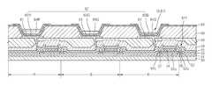
- FIG. 2is a sectional view of one of the pixels of the organic light-emitting display device illustrated in FIG. 1 , according to an embodiment of the present invention.
- a buffer layer 51is formed on a substrate 50 formed of glass or plastic.
- a TFT and an OLEDare formed on the buffer layer 51 .
- An active layer 52 having a predetermined patternis formed on the buffer layer 51 .
- a gate insulating layer 53is formed on the active layer 52 , and a gate electrode 54 is formed in a predetermined region of the gate insulating layer 53 .
- the gate electrode 54is connected to a gate line (not shown) that applies a TFT ON/OFF signal.
- An interlayer insulating layer 55is formed on the gate electrode 54 .
- Source/drain electrodes 56 and 57are formed such as to contact source/drain regions 52 b and 52 c of the active layer 52 through contact holes, respectively.
- a gate region 52 ais disposed between the source/drain regions 52 b and 52 c .
- a passivation layer 58is formed of SiO 2 , SiN x , or the like, on the source/drain electrodes 56 and 57 .
- a planarization layer 59is formed of an organic material, such as acryl, polyimide, benzocyclobutene (BCB), or the like, on the passivation layer 58 .
- a pixel electrode 61which functions as an anode of the OLED, is formed on the planarization layer 59 , and a pixel defining layer 60 is formed of an organic material to cover the pixel electrode 61 .
- An openingis formed in the pixel defining layer 60 , and then an organic layer 62 is formed on the pixel defining layer 60 and the pixel electrode 61 that is exposed through the opening.
- the organic layer 62includes a plurality of emission layers 62 R, 62 G, and 62 B.
- the aspects of the present inventionare not limited to the structure of the organic light-emitting display device described above, and various structures of organic light-emitting display devices may be applied to the aspects of the present invention.
- the OLEDdisplays predetermined image information by emitting red, green and blue light as current flows.
- the OLEDincludes the pixel electrode 61 , which is connected to a drain electrode 57 of the TFT and to which a positive power voltage is applied, a second electrode 63 , which is formed to cover all the pixels and to which a negative power voltage is applied, the organic layer 62 , which is disposed between the pixel electrode 61 and the second electrode 63 to emit light, and a plurality of capping layers (CPL) 64 R, 64 G, and 64 B formed on the second electrode 63 to correspond to a plurality of sub pixels, respectively.
- CPLcapping layers
- the first and second electrode 61 and 63are insulated from each other by the organic layer 62 , and respectively apply voltages of opposite polarities to the organic layer 62 to induce light emission in the organic layer 62 .
- the organic layer 62may include a low-molecular weight organic layer or a high-molecular weight organic layer.
- the organic layer 62may have a single or multi-layer structure including at least one selected from the group consisting of a hole injection layer (HIL), a hole transport layer (HTL), an emission layer (EML), an electron transport layer (ETL), and an electron injection layer (EIL).
- HILhole injection layer
- HTLhole transport layer
- EMLemission layer
- ETLelectron transport layer
- EILelectron injection layer
- the low-molecular weight organic layermay be formed by vacuum deposition.
- the organic layer 62may mostly have a structure including a HTL and an EML.
- the HTLmay be formed of poly(ethylenedioxythiophene) (PEDOT), and the EML may be formed of, for example, a polyphenylenevinylenes (PPVs) or polyfluorenes-based high-molecular weight organic material.
- PVspolyphenylenevinylenes
- the HTL and the EMLmay be formed by screen printing, inkjet printing, or the like.
- the organic layer 62is not limited to the organic layers described above and may be embodied in various ways.
- the first electrode 61functions as an anode, and the second electrode 63 functions as a cathode.
- the first electrode 61may function as a cathode, and the second electrode 63 may function as an anode.
- the first electrode 61may be formed as a transparent electrode or a reflective electrode.
- a transparent electrodemay be formed of an indium tin oxide (ITO), an indium zinc oxide (IZO), a zinc oxide (ZnO), or an indium oxide (In 2 O 3 )
- a reflective electrodemay be formed by forming a reflective layer of silver (Ag), magnesium (Mg), aluminum (Al), platinum (Pt), palladium (Pd), gold (Au), nickel (Ni), neodymium (Nd), iridium (Ir), chromium (Cr) or a compound thereof and forming a layer of ITO, IZO, ZnO, or In 2 O 3 on the reflective layer.
- the second electrode 63may also be formed as a transparent electrode or a reflective electrode.
- the second electrode 63functions as a cathode.
- a transparent electrodemay be formed by depositing a metal having a low work function, such as lithium (Li), calcium (Ca), lithium fluoride/calcium (LiF/Ca), lithium fluoride/aluminum (LiF/AI), aluminum (Al), silver (Ag), magnesium (Mg), or a compound thereof on a surface of the organic layer 62 and forming an auxiliary electrode layer or a bus electrode line thereon from a transparent electrode forming material, such as ITO, IZO, ZnO, In 2 O 3 , or the like.
- the reflective layermay be formed by depositing Li, Ca, LiF/Ca, LiF/Al, Al, Ag, Mg, or a compound thereof on the entire surface of the organic layer 62
- the capping layers (CPL) 64 R, 64 G, and 64 Bincrease the brightness of the OLED and have thicknesses suitable for emitting red, green, and blue lights, respectively.
- a low or high molecular weight organic layermay be used for each of the capping layers (CPL) 64 R, 64 G, and 64 B, and the same material used to form the organic layer 62 may also be used to form the capping layers (CPL) 64 R, 64 G, and 64 B.
- the organic layer 62 including the emission layers 62 R, 62 G, and 62 B and the capping layers (CPL) 64 R, 64 G, and 64 Bmay be formed by using a thin film deposition apparatus 100 (see FIG. 3 ), which will be described later.
- the capping layers (CPL) 64 R, 64 G, and 64 B corresponding to R, G, and B sub-pixels that emit red, green and blue light, respectively,have different thicknesses.
- the first or second electrode 61 or 63is a reflective electrode and the other electrode is a semi-transparent or transparent electrode.
- oscillationmay occur between the first and second electrodes 61 and 63 when the organic light-emitting display device is driven. Since the first or second electrode 61 or 63 is a reflective electrode and the other is a semi-transparent or transparent electrode, when the organic light-emitting display device is driven, lights generated by the respective emission layers 62 R, 62 G, and 62 B between the first and second electrodes 61 and 63 are emitted outside the organic light-emitting display device while oscillating between the first and second electrodes 61 and 63 , thereby increasing the luminance and efficiency of light emission.
- the thicknesses of the emission layers 62 R, 62 G, and 62 B for respective red, green, and blue lightsmay be different from one another in order to maximize oscillation efficiency.
- the capping layers (CPL) 64 R, 64 G, and 64 B corresponding to the sub-pixels that emit red, green, and blue lights, respectively,may be formed to different thicknesses.
- Table 1shows data representing white efficiency when the thicknesses of the capping layers (CPL) 64 R, 64 G, and 64 B are optimally determined.
- white efficiency when the thicknesses of the capping layers (CPL) 64 R, 64 G, and 64 B corresponding to the sub-pixels that emit red, green, and blue lights, respectively, are optimally determinedis improved by 30% or higher than when the thicknesses of the capping layers (CPL) 64 R, 64 G, and 64 B are the same.
- the organic light-emitting display devicesmay have improved driving voltage, current density, brightness, color purity, light-emission efficiency, and lifetime.
- the capping layers (CPL) 64 R, 64 G, and 64 Bmay be formed by performing only a process using a thin film deposition apparatus according to an embodiment of the present invention. This will be described in detail later.
- a thin film deposition apparatus and a method of manufacturing an organic light-emitting display device by using the thin film deposition apparatus according to an embodiment of the present inventionwill now be described in detail.
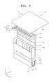
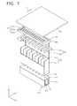
- FIG. 3is a schematic perspective view of a thin film deposition apparatus 100 according to an embodiment of the present invention.
- FIG. 4is a schematic side view of the thin film deposition apparatus 100 of FIG. 3 .
- FIG. 5is a schematic plan view of the thin film deposition apparatus 100 of FIG. 3 .
- the thin film deposition apparatus 100includes a deposition source 110 , a deposition source nozzle unit 120 , a barrier plate assembly 130 , and a patterning slit sheet 150 .
- all the components of the thin film deposition apparatus 100may be disposed within a chamber that is maintained at an appropriate degree of vacuum.
- the chamberis maintained at an appropriate vacuum in order to allow a deposition material to move in a substantially straight line through the thin film deposition apparatus 100 .
- the substrate 600may be a substrate for flat panel displays.
- Other substratesmay also be employed.
- depositionmay be performed while the substrate 600 is moved relative to the thin film deposition apparatus 100 , but the invention is not limited thereto. Therefore, deposition may also be performed while the thin film deposition apparatus 100 is moved relative to the substrate 600 .
- the size of an FMMhas to be equal to the size of a substrate.
- the size of the FMMhas to be increased as the substrate becomes larger.
- depositionmay be performed while the thin film deposition apparatus 100 or the substrate 600 is moved relative to each other.
- depositionmay be continuously performed while the substrate 600 disposed to face the thin film deposition apparatus 100 is moved in a Y-axis direction. That is, deposition is performed in a scanning manner while the substrate 600 is moved in a direction of arrow A in FIG. 3 .
- the substrate 600is illustrated as being moved in the Y-axis direction in FIG. 3 when deposition is performed, the aspects of the present invention are not limited thereto and as noted above deposition may be performed while the thin film deposition apparatus 100 is moved in the Y-axis direction, whereas the substrate 600 is fixed.
- the patterning slit sheet 150may be significantly smaller than the FMM used in the conventional deposition method. That is, in the thin film deposition apparatus 100 , deposition is continuously performed, i.e., in a scanning manner while the substrate 600 is moved in the Y-axis direction. Thus, lengths of the patterning slit sheet 150 may be significantly less than the lengths of the substrate 600 , in the X-axis and Y-axis directions. As described above, since the patterning slit sheet 150 may be formed to be significantly smaller than the FMM used in the conventional deposition method, it is relatively easy to manufacture the patterning slit sheet 150 according to an aspect of the present invention.
- using the patterning slit sheet 150which is smaller than the FMM used in the conventional deposition method, is more convenient in all processes, including etching and subsequent other processes, such as precise extension, welding, moving, and cleaning processes, compared to the conventional deposition method using the larger FMM. This is more advantageous for a relatively large display device.
- the thin film deposition apparatus 100 and the substrate 600may be separated from each other by a predetermined distance. This will be described later in detail.
- the deposition source 110 that contains and heats the deposition material 115is disposed in an opposite side of the chamber to that in which the substrate 600 is disposed. As the deposition material 115 contained in the deposition source 110 is vaporized, the deposition material 115 is deposited on the substrate 600 .
- the deposition source 110includes a crucible 111 that is filled with the deposition material 115 , and a heater 112 that heats the crucible 111 to vaporize the deposition material 115 , which is contained in the crucible 111 , towards a side of the crucible 111 , and in particular, towards the deposition source nozzle unit 120 .
- the deposition source nozzle unit 120is disposed at a side of the deposition source 110 , and in particular, at the side of the deposition source 110 facing the substrate 600 .
- the deposition source nozzle unit 120includes a plurality of deposition source nozzles 121 arranged in the X-axis direction.
- the deposition material 115 that is vaporized in the deposition source 110passes through the deposition source nozzle unit 120 towards the substrate 600 .
- the barrier plate assembly 130is disposed at a side of the deposition source nozzle unit 120 .
- the barrier plate assembly 130includes a plurality of barrier plates 131 , and a barrier plate frame 132 that covers sides of the barrier plates 131 .
- the plurality of barrier plates 131may be arranged parallel to each other at equal intervals in X-axis direction.
- each of the barrier plates 131may be arranged parallel to an YZ plane in FIG. 3 , i.e., perpendicular to the X-axis direction.
- the plurality of barrier plates 131 arranged as described abovepartition the deposition space between the deposition source nozzle unit 120 and the patterning slit sheet 150 into a plurality of sub-deposition spaces S (see FIG. 5 ).
- the deposition spaceis divided by the barrier plates 131 into the sub-deposition spaces S that respectively correspond to the deposition source nozzles 121 through which the deposition material 115 is discharged.
- the barrier plates 131may be respectively disposed between adjacent deposition source nozzles 121 .
- each of the deposition source nozzles 121may be disposed between two adjacent barrier plates 131 .
- the deposition source nozzles 121may be respectively located at the midpoint between two adjacent barrier plates 131 .
- the barrier plates 131partition the deposition space between the deposition source nozzle unit 120 and the patterning slit sheet 150 into the plurality of sub-deposition spaces S, the deposition material 115 discharged through each of the deposition source nozzles 121 is not mixed with the deposition material 115 discharged through the other deposition source nozzles slits 121 , and passes through patterning slits 151 so as to be deposited on the substrate 600 .
- the barrier plates 131guide the deposition material 115 , which is discharged through the deposition source nozzles slits 121 , to move straight, not to flow in the X-axis direction.
- the deposition material 115is forced to move straight by installing the barrier plates 131 , so that a smaller shadow zone may be formed on the substrate 600 compared to a case where no barrier plates are installed.
- the thin film deposition apparatus 100 and the substrate 600may be separated from each other by a predetermined distance. This will be described later in detail.
- the barrier plate frame 132which covers upper and lower sides of the barrier plates 131 , maintains the positions of the barrier plates 131 , and guides the deposition material 115 , which is discharged through the deposition source nozzles 121 , not to flow in the Y-axis direction.
- the barrier plate assembly 130may be constructed to be detachable from the thin film deposition apparatus 100 .
- a conventional FMM deposition methodhas low deposition efficiency.
- the deposition spaceis enclosed by using the barrier plate assembly 130 , so that the deposition material 115 that remains undeposited is mostly deposited within the barrier plate assembly 130 .
- the barrier plate assembly 130since the barrier plate assembly 130 is constructed to be detachable from the thin film deposition apparatus 100 , when a large amount of the deposition material 115 lies in the barrier plate assembly 130 after a long deposition process, the barrier plate assembly 130 may be detached from the thin film deposition apparatus 100 and then placed in a separate deposition material recycling apparatus in order to recover the deposition material 115 . Due to the structure of the thin film deposition apparatus 100 , a reuse rate of the deposition material 115 is increased, improving the deposition efficiency, thus reducing manufacturing costs.
- the patterning slit sheet 150 and a frame 155are disposed between the deposition source 110 and the substrate 600 .
- the frame 155may be formed in a lattice shape, similar to a window frame.
- the patterning slit sheet 150bounds the frame 155 .
- the patterning slit sheet 150includes a plurality of patterning slits 151 arranged in the X-axis direction.
- the deposition material 115 that is vaporized in the deposition source 110passes through the deposition source nozzle unit 120 and the patterning slit sheet 150 towards the substrate 600 .
- the patterning slit sheet 150may be manufactured by etching, which is the same method as used in the conventional method of manufacturing the FMM, and in particular, a striped FMM.
- Each of the patterning slits 151includes a plurality of patterning sub slits 151 a to 151 c that are different in lengths. This will be described in detail with reference to FIG. 6 later.
- the total number of patterning slits 151may be greater than the total number of deposition source nozzles 121 .
- one deposition source nozzle 121may be disposed between each two adjacent barrier plates 131 .
- a plurality of patterning slits 151may be disposed between each two adjacent barrier plates 131 .
- the deposition space between the deposition source nozzle unit 120 and the patterning slit sheet 150is partitioned by the barrier plates 131 into sub-deposition spaces S that correspond to the deposition source nozzles 121 , respectively.
- the deposition material 115 discharged from each of the deposition source nozzles 121passes through a plurality of patterning slits 151 disposed in the sub-deposition space S corresponding to the deposition source nozzle 121 , and is then deposited on the substrate 600 .
- the barrier plate assembly 130 and the patterning slit sheet 150may be formed to be separated from each other by a predetermined distance.
- the barrier plate assembly 130 and the patterning slit sheet 150may be connected by a connection unit 135 .
- the temperature of the barrier plate assembly 130may increase to 100° C. or higher due to the deposition source 110 whose temperature is high.
- the barrier plate assembly 130 and the patterning slit sheet 150are separated from each other by the predetermined distance.
- the thin film deposition apparatus 100performs deposition while being moved relative to the substrate 600 .
- the patterning slit sheet 150is separated from the substrate 600 by the predetermined distance.
- the barrier plates 131are arranged between the deposition source nozzle unit 120 and the patterning slit sheet 150 to force the deposition material 115 to move in a straight direction.
- the size of the shadow zone formed on the substrate 400is sharply reduced.
- the FMMin the conventional deposition method using the FMM, deposition is performed with the FMM in close contact with a substrate in order to prevent formation of a shadow zone on the substrate.
- the contactmay cause defects.
- the size of the maskhas to be the same as the size of the substrate since the mask cannot be moved relative to the substrate.
- the size of the maskhas to be increased as display devices become larger but it is not easy to manufacture such a large mask.
- the patterning slit sheet 150is disposed to be separated from the substrate 600 by the predetermined distance. This may be facilitated by installing the barrier plates 131 to reduce the size of the shadow zone formed on the substrate 600 .
- a maskis formed to be smaller than a substrate, and deposition is performed while the mask is moved relative to the substrate.
- the maskcan be easily manufactured.
- defects caused due to the contact between a substrate and a FMM, which occurs in the conventional deposition methodmay be prevented.
- the manufacturing speedmay be improved.
- the shadow zone formed on the substrate 600may be reduced by installing the barrier plates 131 .
- the patterning slit sheet 150can be separated from the substrate 600 .
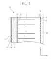
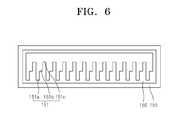
- FIG. 6is a plan view of the patterning slit sheet 150 included in the thin film deposition apparatus 100 of FIG. 3 , according to an embodiment of the present invention.
- each of the patterning slits 151includes the plurality of patterning sub slits 151 a to 151 c that are different in length.
- the capping layers 64 R, 64 G, and 64 B corresponding to sub pixels that emit red, green, and blue lights, respectively,have different thicknesses from one another. That is, the thickness of the capping layer 64 R corresponding to a red sub pixel that emits red light may be relative thick, the thickness of the capping layer 64 G corresponding to a green sub pixel that emits green light may be thinner than that of the capping layer 64 R, and the thickness of the capping layer 64 B corresponding to a blue sub pixel that emits blue light may be thinner than that of the capping layer 64 G.
- a capping layer corresponding to a red sub pixel that emits red light, a capping layer corresponding to a green sub pixel that emits green light, and a capping layer corresponding to a blue sub pixel that emits blue lightare therefore formed separately.
- the capping layers 64 R, 64 G, and 64 Bare formed of the same material and are different from one another only in terms of their location and thickness.
- the capping layers 64 R, 64 G, and 64 B that correspond to the red, green, and blue sub pixels, respectively,are formed subsequently in such a manner that regions of each of the patterning slits 151 , which correspond to red, green, and blue sub pixel regions, respectively, are different from one another in length.
- each of the patterning slits 151includes a first patterning slit 151 a , a second patterning slit 151 b , and a third patterning slit 151 c .
- the first patterning slit 151 acorresponds to the red sub pixel region
- the second patterning slit 151 bcorresponds to the green sub pixel region
- the third patterning slit 151 ccorresponds to the blue sub pixel region. That is, referring to FIG. 5 , since the deposition material 115 that passes through the patterning slits 151 is deposited on the substrate 600 , the greater the patterning slit 151 , the thicker an organic layer to be formed on the substrate 600 .
- the first patterning slit 151 a for forming the capping layer 64 R corresponding to the red sub pixel, the thickness of which is relatively thickis the longest
- the second patterning slit 151 b for forming the capping layer 64 G corresponding to the green sub pixelis shorter than the first patterning slit 151 a
- the third patterning slit 151 c for forming the capping layer 64 B corresponding to the blue sub pixelthe thickness of which is thinner than the capping layer 64 R is shorter than the second patterning slit 151 b.
- the patterning slit sheet 150is formed in such a manner that an upper portion of the patterning slit sheet 150 may be used as a common deposition region and a plurality of slits having different lengths, which correspond to the red, green, and blue sub pixels, respectively, are alternately and repeatedly formed in a lower portion of the patterning slit 151 .
- each of patterning slitshas sub patterning slits that are different in length, in which long patterning sub slits correspond to portions of a substrate on which a large amount of a deposition material is to be deposited so that the large amount of the deposition material may pass through the long patterning slits, and short patterning sub slits correspond to portions of the substrate on which a small amount of the deposition material is to be deposited so that the small amount of the deposition material may pass through the short patterning slits.
- two layersmay be formed at a time, thereby reducing the total number of thin film deposition apparatuses needed, reducing a time needed to manufacture the thin film deposition apparatuses, and simplifying equipment for manufacturing the thin film deposition apparatuses.
- FIG. 7is a schematic perspective view of a thin film deposition apparatus 500 according to another embodiment of the present invention.
- the thin film deposition apparatus 500includes a deposition source 510 , a deposition source nozzle unit 520 , a first barrier plate assembly 530 , a second barrier plate assembly 540 , a patterning slit sheet 550 , and a substrate 600 .
- all the components of the thin film deposition apparatus 500may be disposed within a chamber that is maintained at an appropriate degree of vacuum.
- the chamberis maintained at an appropriate vacuum in order to allow a deposition material to move in a substantially straight line through the thin film deposition apparatus 500 .
- the substrate 600 that is a deposition targetis disposed in the chamber.
- the deposition source 510 that contains and heats a deposition material 515is disposed in an opposite side of the chamber to that in which the substrate 600 is disposed.
- the deposition source 510may include a crucible 511 and a heater 512 .
- the deposition source nozzle unit 520is disposed at a side of the deposition source 510 , and in particular, at the side of the deposition source 510 facing the substrate 600 .
- the deposition source nozzle unit 520includes a plurality of deposition source nozzles 521 arranged in the X-axis direction.
- the first barrier plate assembly 530is disposed at a side of the deposition source nozzle unit 520 .
- the first barrier plate assembly 530includes a plurality of first barrier plates 531 , and a first barrier plate frame 532 that covers sides of the first barrier plates 531 .
- the second barrier plate assembly 540is disposed at a side of the first barrier plate assembly 530 .
- the second barrier plate assembly 540includes a plurality of second barrier plates 541 , and a second barrier plate frame 542 that covers sides of the second barrier plates 541 .
- the patterning slit sheet 550 and a frame 555 in which the patterning slit sheet 550 is boundare disposed between the deposition source 510 and the substrate 600 .
- the frame 555may be formed in a lattice shape, similar to a window frame.
- the patterning slit sheet 550includes a plurality of patterning slits 551 arranged in the X-axis direction.
- the thin film deposition apparatus 500includes two separate barrier plate assemblies, i.e., the first barrier plate assembly 530 and the second barrier plate assembly 540 .
- the plurality of first barrier plates 531may be arranged parallel to each other at equal intervals in the X-axis direction.
- Each of the first barrier plates 531may be formed to extend along an YZ plane in FIG. 7 , i.e., perpendicular to the X-axis direction.
- the plurality of second barrier plates 541may be arranged parallel to each other at equal intervals in the X-axis direction.
- each of the second barrier plates 541may be formed to extend in the YZ plane in FIG. 7 , i.e., perpendicular to the X-axis direction.
- the deposition spaceis divided by the first barrier plates 531 and the second barrier plates 541 into sub-deposition spaces that respectively correspond to the deposition source nozzles 521 through which the deposition material 515 is discharged.
- the second barrier plates 541may be disposed to correspond respectively to the first barrier plates 531 .
- the second barrier plates 541may be aligned with the first barrier plates 531 , respectively.
- Each pair of the corresponding first and second barrier plates 531 and 541may be located on the same plane.
- the deposition space between the deposition source nozzle unit 520 and the patterning slit sheet 550which will be described later, is partitioned by the first barrier plates 531 and the second barrier plates 541 , which are disposed parallel to each other, the deposition material 515 discharged through one of the deposition source nozzles 521 is not mixed with the deposition material 515 discharged through the other deposition source nozzles 521 , and is deposited on the substrate 600 through the patterning slits 551 .
- the first barrier plates 531 and the second barrier plates 541guide the deposition material 515 , which is discharged through the deposition source nozzles 521 , not to flow in the X-axis direction.
- first barrier plates 531 and the second barrier plates 541are respectively illustrated as having the same thickness in the X-axis direction, the aspects of the present invention are not limited thereto.
- the second barrier plates 541which need to be accurately aligned with the patterning slit sheet 550 , may be formed to be relatively thin, whereas the first barrier plates 531 , which do not need to be precisely aligned with the patterning slit sheet 550 , may be formed to be relatively thick. This makes it easier to manufacture the thin film deposition apparatus 500 .
- FIG. 8is a schematic perspective view of a thin film deposition apparatus 700 according to another embodiment of the present invention.
- FIG. 9is a schematic side view of the thin film deposition apparatus 700 illustrated in FIG. 8 .
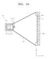
- FIG. 10is a schematic plan view of the thin film deposition apparatus 700 illustrated in FIG. 8 .
- the thin film deposition apparatus 700includes a deposition source 710 , a deposition source nozzle unit 720 , a patterning slit sheet 750 and a frame 755 .
- all the components of the thin film deposition apparatus 700may be disposed within a chamber that is maintained at an appropriate degree of vacuum.
- the chamberis maintained at an appropriate vacuum in order to allow a deposition material to move in a substantially straight line through the thin film deposition apparatus 700 .
- a substrate 600 that is a deposition targetis disposed in the chamber.
- the deposition source 710 that contains and heats a deposition material 715is disposed in an opposite side of the chamber to that in which the substrate 600 is disposed.
- the deposition source 710may include a crucible 711 and a heater 712 .
- the deposition source nozzle unit 720is disposed at a side of the deposition source 710 , and in particular, at the side of the deposition source 710 facing the substrate 600 .
- the deposition source nozzle unit 720includes a plurality of deposition source nozzles 721 arranged in the Y-axis direction, i.e., a scanning direction of the substrate 600 .
- the plurality of deposition source nozzles 721may be disposed at equal intervals.
- the deposition material 715 that is vaporized in the deposition source 710passes through the deposition source nozzle unit 720 towards the substrate 600 .
- a size of a pattern formed by the deposition material 715 that is discharged through each of patterning slits 751 in the patterning slit sheet 750is only affected by the size of one deposition source nozzle 721 , that is, it may be considered that one deposition nozzle 721 exists in the X-axis direction. Thus, there is no shadow zone on the substrate 600 .
- the plurality of deposition source nozzles 721are formed in the scanning direction of the substrate 600 , even there is a difference between fluxes of the deposition source nozzles 721 , the difference may be compensated for and deposition uniformity may be maintained constantly.
- the patterning slit sheet 750 and a frame 755are disposed between the deposition source 710 and the substrate 600 .
- the frame 755may be formed in a lattice shape, similar to a window frame.
- the patterning slit sheet 750is bound inside the frame 755 .
- the patterning slit sheet 750includes a plurality of patterning slits 751 arranged in the X-axis direction.
- the deposition material 715 that is vaporized in the deposition source 710passes through the deposition source nozzle unit 720 and the patterning slit sheet 750 towards the substrate 600 .
- the patterning slit sheet 750may be manufactured by etching, which is the same method as used in a conventional method of manufacturing an FMM, and in particular, a striped FMM.
- each of the patterning slits 751includes sub slits that are different in length.
- a capping layer corresponding to a red sub pixel, a capping layer corresponding to a green sub pixel, and a capping layer corresponding to a blue sub pixelmay be sequentially formed. That is, each of the patterning slits 751 includes a first patterning sub slit 751 a , a second patterning sub slit 751 b , and a third patterning sub slit 751 c .
- the first patterning slit 751 acorresponds to a red sub pixel region
- the second patterning slit 751 bcorresponds to a green sub pixel region
- the third patterning slit 751 ccorresponds to a blue sub pixel region.
- the first patterning slit 751 a for forming the capping layer corresponding to the red sub pixel, the thickness of which is relative thick (see the capping layer 64 R of FIG. 2 )may be longest
- the second patterning slit 751 b for forming the capping layer corresponding to the green sub pixel, the thickness of which is thinner than the capping layer corresponding to the red sub pixel (see the capping layer 64 G of FIG. 2 )may be shorter than the first patterning slit 751 a
- the capping layer corresponding to the blue sub pixel, the thickness of which is thinner than the capping layer corresponding to the green sub pixel (see the capping layer 64 B of FIG. 2 )may be shorter than the second patterning slit 751 b .
- the patterning slits 751are as described above with reference to FIG. 3 .
- the deposition source 710 (and the deposition source nozzle unit 720 coupled to the deposition source 710 ) and the patterning slit sheet 750may be formed to be separated from each other by a predetermined distance.
- the deposition source 710 (and the deposition source nozzle unit 720 coupled to the deposition source 710 ) and the patterning slit sheet 750may be connected by a connection unit 735 . That is, the deposition source 710 , the deposition source nozzle unit 720 , and the patterning slit sheet 750 may be formed integrally with one another by being connected to each other via the connection unit 735 .
- connection unit 735guides the deposition material 715 , which is discharged through the deposition source nozzles 721 , to move straight, not to flow in the X-axis direction.
- the connection units 735are formed on left and right sides of the deposition source 710 , the deposition source nozzle unit 720 , and the patterning slit sheet 750 to guide the deposition material 715 not to flow in the X-axis direction, however, the aspects of the present invention are not limited thereto.
- connection units 735may be formed to seal the deposition source 710 , the deposition source nozzle unit 720 , and the patterning slit sheet 750 in the form of a box in order to guide the deposition material 715 in both the X-axis and Y-axis directions.
- the thin film deposition apparatus 700performs deposition while being moved relative to the substrate 600 .
- the patterning slit sheet 750is separated from the substrate 600 by a predetermined distance.
- a maskis formed to be smaller than a substrate and deposition is performed while the mask is moved relative to the substrate.
- the maskcan be easily manufactured.
- defects caused due to the contact between a substrate and an FMM, which occurs in the conventional deposition methodmay be prevented.
- the manufacturing speedmay be improved.
- a thin film deposition apparatusAs described above, a thin film deposition apparatus, a method of manufacturing an organic light-emitting display device by using the thin film deposition apparatus, and an organic light-emitting display device manufactured using the method according to an aspect of the present invention may be simply applied to manufacture large-sized display devices on a mass scale.
- the thin film deposition apparatus and the organic-light-emitting display devicemay be easily manufactured and may improve manufacturing yield and deposition efficiency.
Landscapes
- Chemical & Material Sciences (AREA)
- Engineering & Computer Science (AREA)
- Chemical Kinetics & Catalysis (AREA)
- Materials Engineering (AREA)
- Mechanical Engineering (AREA)
- Metallurgy (AREA)
- Organic Chemistry (AREA)
- Manufacturing & Machinery (AREA)
- Electroluminescent Light Sources (AREA)
- Physical Vapour Deposition (AREA)
Abstract
Description
| TABLE 1 | ||||
| R | G | B | ||
| CPL efficiency (cd/A) when | 30.8 | 40.2 | 2.6 | |
| the capping layers (CPL) | ||||
| 64R, 64G, and 64B have | ||||
| the same thickness | ||||
| CPL efficiency (cd/A) when | 30.8 | 43.4 | 3.9 | |
| the thicknesses of the | ||||
| capping layers (CPL) 64R, | ||||
| 64G, and 64B are optimally | ||||
| determined |
| White | 16.9 -> 21.5 | ||
| Efficiency | |||
Claims (34)
Applications Claiming Priority (2)
| Application Number | Priority Date | Filing Date | Title |
|---|---|---|---|
| KR10-2010-0009160 | 2010-02-01 | ||
| KR1020100009160AKR101193186B1 (en) | 2010-02-01 | 2010-02-01 | Apparatus for thin layer deposition, method for manufacturing of organic light emitting display apparatus using the same, and organic light emitting display apparatus manufactured by the method |
Publications (2)
| Publication Number | Publication Date |
|---|---|
| US20110186820A1 US20110186820A1 (en) | 2011-08-04 |
| US8882556B2true US8882556B2 (en) | 2014-11-11 |
Family
ID=44316268
Family Applications (1)
| Application Number | Title | Priority Date | Filing Date |
|---|---|---|---|
| US12/984,289Active2031-09-08US8882556B2 (en) | 2010-02-01 | 2011-01-04 | Thin film deposition apparatus, method of manufacturing organic light-emitting display device by using the apparatus, and organic light-emitting display device manufactured by using the method |
Country Status (6)
| Country | Link |
|---|---|
| US (1) | US8882556B2 (en) |
| JP (1) | JP5622559B2 (en) |
| KR (1) | KR101193186B1 (en) |
| CN (1) | CN102169968B (en) |
| DE (1) | DE102011003458A1 (en) |
| TW (1) | TWI607598B (en) |
Cited By (2)
| Publication number | Priority date | Publication date | Assignee | Title |
|---|---|---|---|---|
| US20190226078A1 (en)* | 2010-01-11 | 2019-07-25 | Samsung Display Co., Ltd. | Thin film deposition apparatus |
| US12442069B2 (en)* | 2010-01-11 | 2025-10-14 | Samsung Display Co., Ltd. | Thin film deposition apparatus |
Families Citing this family (46)
| Publication number | Priority date | Publication date | Assignee | Title |
|---|---|---|---|---|
| US8882920B2 (en)* | 2009-06-05 | 2014-11-11 | Samsung Display Co., Ltd. | Thin film deposition apparatus |
| JP5328726B2 (en) | 2009-08-25 | 2013-10-30 | 三星ディスプレイ株式會社 | Thin film deposition apparatus and organic light emitting display device manufacturing method using the same |
| JP5677785B2 (en) | 2009-08-27 | 2015-02-25 | 三星ディスプレイ株式會社Samsung Display Co.,Ltd. | Thin film deposition apparatus and organic light emitting display device manufacturing method using the same |
| US8876975B2 (en) | 2009-10-19 | 2014-11-04 | Samsung Display Co., Ltd. | Thin film deposition apparatus |
| KR101146982B1 (en) | 2009-11-20 | 2012-05-22 | 삼성모바일디스플레이주식회사 | Aapparatus for thin layer deposition and method of manufacturing organic light emitting display apparatus |
| KR101193186B1 (en) | 2010-02-01 | 2012-10-19 | 삼성디스플레이 주식회사 | Apparatus for thin layer deposition, method for manufacturing of organic light emitting display apparatus using the same, and organic light emitting display apparatus manufactured by the method |
| KR101156441B1 (en) | 2010-03-11 | 2012-06-18 | 삼성모바일디스플레이주식회사 | Apparatus for thin layer deposition |
| US8894458B2 (en) | 2010-04-28 | 2014-11-25 | Samsung Display Co., Ltd. | Thin film deposition apparatus, method of manufacturing organic light-emitting display device by using the apparatus, and organic light-emitting display device manufactured by using the method |
| KR101223723B1 (en) | 2010-07-07 | 2013-01-18 | 삼성디스플레이 주식회사 | Apparatus for thin layer deposition, method for manufacturing of organic light emitting display apparatus using the same, and organic light emitting display apparatus manufactured by the method |
| JP5307940B2 (en) | 2010-09-27 | 2013-10-02 | シャープ株式会社 | Vapor deposition method, vapor deposition apparatus, and organic EL display apparatus |
| KR101723506B1 (en) | 2010-10-22 | 2017-04-19 | 삼성디스플레이 주식회사 | Apparatus for organic layer deposition and method for manufacturing of organic light emitting display apparatus using the same |
| KR101738531B1 (en) | 2010-10-22 | 2017-05-23 | 삼성디스플레이 주식회사 | Method for manufacturing of organic light emitting display apparatus, and organic light emitting display apparatus manufactured by the method |
| KR20120045865A (en) | 2010-11-01 | 2012-05-09 | 삼성모바일디스플레이주식회사 | Apparatus for organic layer deposition |
| KR20120065789A (en) | 2010-12-13 | 2012-06-21 | 삼성모바일디스플레이주식회사 | Apparatus for organic layer deposition |
| KR101760897B1 (en) | 2011-01-12 | 2017-07-25 | 삼성디스플레이 주식회사 | Deposition source and apparatus for organic layer deposition having the same |
| KR101840654B1 (en) | 2011-05-25 | 2018-03-22 | 삼성디스플레이 주식회사 | Apparatus for organic layer deposition and method for manufacturing of organic light emitting display apparatus using the same |
| KR101852517B1 (en) | 2011-05-25 | 2018-04-27 | 삼성디스플레이 주식회사 | Apparatus for organic layer deposition and method for manufacturing of organic light emitting display apparatus using the same |
| KR101857249B1 (en) | 2011-05-27 | 2018-05-14 | 삼성디스플레이 주식회사 | Patterning slit sheet assembly, apparatus for organic layer deposition, method for manufacturing organic light emitting display apparatus and organic light emitting display apparatus |
| US8884316B2 (en)* | 2011-06-17 | 2014-11-11 | Universal Display Corporation | Non-common capping layer on an organic device |
| KR101826068B1 (en) | 2011-07-04 | 2018-02-07 | 삼성디스플레이 주식회사 | Apparatus for thin layer deposition |
| KR101959975B1 (en)* | 2012-07-10 | 2019-07-16 | 삼성디스플레이 주식회사 | Apparatus for organic layer deposition, method for manufacturing of organic light emitting display apparatus using the same, and organic light emitting display apparatus manufactured by the method |
| KR101990116B1 (en)* | 2012-10-22 | 2019-10-01 | 삼성디스플레이 주식회사 | Organic light emitting device and manufacture method thereof |
| KR102009726B1 (en)* | 2012-11-08 | 2019-10-22 | 삼성디스플레이 주식회사 | Organic light emitting display apparatus and method for manufacturing the same |
| KR102046157B1 (en)* | 2012-12-21 | 2019-12-03 | 삼성디스플레이 주식회사 | Organic light emitting diode display and manufacturing method thereof |
| KR102017118B1 (en)* | 2013-01-03 | 2019-09-03 | 삼성디스플레이 주식회사 | Organic light emitting device and method of manufacturing the same |
| JP6136578B2 (en)* | 2013-05-29 | 2017-05-31 | ソニー株式会社 | DISPLAY DEVICE, DISPLAY DEVICE MANUFACTURING METHOD, AND ELECTRONIC DEVICE |
| KR102216676B1 (en)* | 2014-07-07 | 2021-02-18 | 삼성디스플레이 주식회사 | Apparatus for thin layer deposition, and method for manufacturing of organic light emitting display apparatus using the same |
| US9905813B2 (en)* | 2015-06-29 | 2018-02-27 | Samsung Display Co., Ltd. | Organic light-emitting display device, organic layer depositing apparatus, and method of manufacturing organic light-emitting display device using the organic layer depositing apparatus |
| KR20180075589A (en) | 2015-10-26 | 2018-07-04 | 오티아이 루미오닉스 인크. | A method of patterning a coating on a surface and a device comprising a patterned coating |
| KR102440237B1 (en)* | 2015-11-03 | 2022-09-05 | 엘지디스플레이 주식회사 | Organic light emitting diode display device |
| JP7056964B2 (en) | 2016-12-02 | 2022-04-19 | オーティーアイ ルミオニクス インコーポレーテッド | Devices with conductive coatings placed over the radiating region and methods for them |
| JP2020518107A (en) | 2017-04-26 | 2020-06-18 | オーティーアイ ルミオニクス インコーポレーテッドOti Lumionics Inc. | Method for patterning a coating on a surface and device containing the patterned coating |
| CN110832660B (en) | 2017-05-17 | 2023-07-28 | Oti照明公司 | Method for selectively depositing conductive coating on patterned coating and device comprising conductive coating |
| US11751415B2 (en) | 2018-02-02 | 2023-09-05 | Oti Lumionics Inc. | Materials for forming a nucleation-inhibiting coating and devices incorporating same |
| CN112074966A (en) | 2018-05-07 | 2020-12-11 | Oti照明公司 | Method for providing an auxiliary electrode and device comprising an auxiliary electrode |
| KR20240134065A (en) | 2018-11-23 | 2024-09-05 | 오티아이 루미오닉스 인크. | Optoelectronic device including a light transmissive region |
| CN116456753A (en) | 2019-03-07 | 2023-07-18 | Oti照明公司 | an optoelectronic device |
| KR102831863B1 (en) | 2019-04-18 | 2025-07-10 | 오티아이 루미오닉스 인크. | Material for forming a nucleation-inhibiting coating and device comprising the same |
| CN114072705A (en) | 2019-05-08 | 2022-02-18 | Oti照明公司 | Material for forming nucleation inhibiting coatings and apparatus incorporating the same |
| JP7386556B2 (en) | 2019-06-26 | 2023-11-27 | オーティーアイ ルミオニクス インコーポレーテッド | Optoelectronic devices containing optically transparent regions with applications related to optical diffraction properties |
| US11832473B2 (en) | 2019-06-26 | 2023-11-28 | Oti Lumionics Inc. | Optoelectronic device including light transmissive regions, with light diffraction characteristics |
| CN114342068A (en) | 2019-08-09 | 2022-04-12 | Oti照明公司 | Optoelectronic device containing auxiliary electrodes and partitions |
| CN111129359A (en)* | 2019-12-09 | 2020-05-08 | 武汉华星光电半导体显示技术有限公司 | Mask plate group, OLED panel and preparation method thereof |
| KR20220131245A (en) | 2019-12-24 | 2022-09-27 | 오티아이 루미오닉스 인크. | Light emitting device including capping layer and manufacturing method thereof |
| KR20220018140A (en)* | 2020-08-05 | 2022-02-15 | 삼성디스플레이 주식회사 | Light emitting device and manufacturing method of the same |
| KR20250139404A (en) | 2020-12-07 | 2025-09-23 | 오티아이 루미오닉스 인크. | Patterning a conductive deposited layer using a nucleation inhibiting coating and an underlying metallic coating |
Citations (469)
| Publication number | Priority date | Publication date | Assignee | Title |
|---|---|---|---|---|
| JPS57194252U (en) | 1981-06-02 | 1982-12-09 | ||
| US4416217A (en) | 1981-07-31 | 1983-11-22 | Ulvac Seimaku Kabushiki Kaisha | Apparatus for forming an inhomogeneous optical layer |
| US4468648A (en) | 1982-10-15 | 1984-08-28 | Mamoru Uchikune | Switchable permanent magnetic chuck |
| US4687939A (en) | 1983-11-07 | 1987-08-18 | Hitachi, Ltd. | Method and apparatus for forming film by ion beam |
| US4792378A (en) | 1987-12-15 | 1988-12-20 | Texas Instruments Incorporated | Gas dispersion disk for use in plasma enhanced chemical vapor deposition reactor |
| US4901667A (en) | 1985-08-09 | 1990-02-20 | Hitachi, Ltd. | Surface treatment apparatus |
| JPH02247372A (en) | 1989-03-17 | 1990-10-03 | Mitsubishi Electric Corp | Thin film deposition method |
| JPH04272170A (en) | 1991-02-25 | 1992-09-28 | Tokai Carbon Co Ltd | Graphite crucible for vacuum deposition |
| JPH05230628A (en) | 1992-02-18 | 1993-09-07 | Fujitsu Ltd | Metal film forming apparatus, metal material recovery method in metal film forming apparatus |
| US5454847A (en) | 1992-09-18 | 1995-10-03 | Alcatel Alsthom Compagnie Generale D'electricite | Vapor deposition method for depositing a film of fluorine-containing glass on a substrate |
| US5460654A (en) | 1992-07-01 | 1995-10-24 | Fujitsu Limited | Apparatus for generating raw material gas used in apparatus for growing thin film |
| US5487609A (en) | 1991-05-13 | 1996-01-30 | Thk Co., Ltd. | Slide unit for linear motion |
| JPH0827568B2 (en) | 1990-07-02 | 1996-03-21 | 三田工業株式会社 | Transfer paper separating device in image forming apparatus |
| JPH0995776A (en) | 1995-09-29 | 1997-04-08 | Sony Corp | Vacuum deposition device |
| JPH1050478A (en) | 1996-04-19 | 1998-02-20 | Toray Ind Inc | Organic electroluminescent device and method of manufacturing the same |
| US5742129A (en) | 1995-02-21 | 1998-04-21 | Pioneer Electronic Corporation | Organic electroluminescent display panel with projecting ramparts and method for manufacturing the same |
| JPH10120171A (en) | 1996-10-15 | 1998-05-12 | Balzers Ag | Equipment for transferring substrates in a vacuum processing system |
| JPH10270535A (en) | 1997-03-25 | 1998-10-09 | Nikon Corp | Moving stage device and circuit device manufacturing method using the stage device |
| WO1999025894A1 (en) | 1997-11-17 | 1999-05-27 | The Trustees Of Princeton University | Low pressure vapor phase deposition of organic thin films |
| JPH11144865A (en) | 1997-11-05 | 1999-05-28 | Casio Comput Co Ltd | Method for manufacturing organic electroluminescence device |
| JP2000068054A (en) | 1998-08-26 | 2000-03-03 | Hokuriku Electric Ind Co Ltd | Manufacture of el element |
| US6045671A (en) | 1994-10-18 | 2000-04-04 | Symyx Technologies, Inc. | Systems and methods for the combinatorial synthesis of novel materials |
| KR20000023929A (en) | 1999-10-29 | 2000-05-06 | 최중호 | Apparatus and method for emitting odor |
| KR100257219B1 (en) | 1997-10-23 | 2000-05-15 | 박용관 | Method and device for making a safety operation of a polyethylene gas pipe valve arrangement |
| US6091195A (en)* | 1997-02-03 | 2000-07-18 | The Trustees Of Princeton University | Displays having mesa pixel configuration |
| US6099649A (en) | 1997-12-23 | 2000-08-08 | Applied Materials, Inc. | Chemical vapor deposition hot-trap for unreacted precursor conversion and effluent removal |
| JP2000282219A (en) | 1999-04-02 | 2000-10-10 | Canon Inc | Method and apparatus for regenerating mask for vacuum deposition of organic film |
| KR20000019254U (en) | 1999-04-07 | 2000-11-06 | 손대균 | Roundin WheeL |
| JP2000323277A (en) | 1999-05-12 | 2000-11-24 | Pioneer Electronic Corp | Organic electroluminescent multicolor display and method of manufacturing the same |
| JP2001052862A (en) | 1999-08-04 | 2001-02-23 | Hokuriku Electric Ind Co Ltd | Manufacture of organic el element and device therefor |
| JP2001093667A (en) | 1999-09-28 | 2001-04-06 | Sanyo Electric Co Ltd | Organic light-emitting element, device and method for manufacturing the same |
| KR20010030175A (en) | 1999-09-01 | 2001-04-16 | 이데이 노부유끼 | Plane display unit and plane display apparatus |
| KR20010039298A (en) | 1999-10-29 | 2001-05-15 | 김영남 | Field emission display |
| US20010004186A1 (en) | 1999-12-10 | 2001-06-21 | Song Gi-Young | Shadow mask frame assembly for flat CRT |
| US20010006827A1 (en) | 1999-12-27 | 2001-07-05 | Semiconductor Energy Laboratory Co., Ltd. | Film formation apparatus and method for forming a film |
| KR20010059939A (en) | 1999-12-30 | 2001-07-06 | 송문섭 | Mobile station for mobile communication system |
| US6274198B1 (en) | 1997-02-24 | 2001-08-14 | Agere Systems Optoelectronics Guardian Corp. | Shadow mask deposition |
| US6280821B1 (en) | 1998-09-10 | 2001-08-28 | Ppg Industries Ohio, Inc. | Reusable mask and method for coating substrate |
| US20010019807A1 (en) | 1999-12-24 | 2001-09-06 | Tsutomu Yamada | Deposition mask and manufacturing method thereof, and electroluminescence display device and manufacturing method thereof |
| US20010026638A1 (en) | 2000-03-28 | 2001-10-04 | Katsuya Sangu | Positioning apparatus used in a process for producing multi-layered printed circuit board and method of using the same |
| US20010034175A1 (en) | 2000-02-16 | 2001-10-25 | Toshihiko Miyazaki | Method and apparatus for manufacturing image displaying apparatus |
| KR20010092914A (en) | 2000-03-27 | 2001-10-27 | 윤종용 | Electrical static chuck comprising a shadow ring |
| KR200257218Y1 (en) | 2001-09-07 | 2001-12-24 | 엘지.필립스 엘시디 주식회사 | Mask apparatus for organic electro-luminescence device |
| KR20020000201A (en) | 2000-06-23 | 2002-01-05 | 최승락 | Method cleaning Liquid Chrystal Display using Laser and Vapor Phase |
| KR20020001555A (en) | 2000-06-22 | 2002-01-09 | 키도 준지 | Apparatus for and method of vacuum vapor deposition and organic electroluminescent device |
| US20020011785A1 (en) | 1998-11-18 | 2002-01-31 | Ching W. Tang | A full color active matrix organic electroluminescent display panel having an integrated shadow mask |
| JP2002075638A (en) | 2000-08-29 | 2002-03-15 | Nec Corp | Vapor deposition method of mask and vapor deposition device |
| US20020033136A1 (en) | 1999-04-02 | 2002-03-21 | Silicon Valley Group, Thermal Systems Llc. | Semiconductor wafer processing system with vertically-stacked process chambers and single-axis dual-wafer transfer system |
| US20020036759A1 (en) | 2000-09-25 | 2002-03-28 | Masaru Ise | Automatic exposing apparatus for both sides and exposing method thereof for works |
| KR20020025760A (en) | 2000-09-28 | 2002-04-04 | 다카노 야스아키 | Method of attaching layer material and forming layer in predetermined pattern on substrate using mask |
| US6371451B1 (en) | 1999-10-29 | 2002-04-16 | Korea Institute Of Science And Technology | Scent diffusion apparatus and method |
| US20020050061A1 (en) | 2000-06-29 | 2002-05-02 | Daido Komyoji | Method and apparatus for forming pattern onto panel substrate |
| KR20020050922A (en) | 2000-12-22 | 2002-06-28 | 박종섭 | Virtual channel sdram |
| US6417034B2 (en) | 2000-05-01 | 2002-07-09 | Nec Corporation | Manufacturing method for organic EL device |
| US20020168577A1 (en) | 2001-05-11 | 2002-11-14 | Jin-Mo Yoon | Method of crystallizing amorphous silicon |
| US6483690B1 (en) | 2001-06-28 | 2002-11-19 | Lam Research Corporation | Ceramic electrostatic chuck assembly and method of making |
| KR20020090934A (en) | 2002-08-27 | 2002-12-05 | 에이엔 에스 주식회사 | Organic material point source feeding unit in organic semiconductor device and method thereof |
| US20020179013A1 (en) | 2001-05-23 | 2002-12-05 | Junji Kido | Successive vapour deposition system, vapour deposition system, and vapour deposition process |
| KR20020091457A (en) | 2001-05-30 | 2002-12-06 | 주식회사 현대 디스플레이 테크놀로지 | Method for control color property of tft-lcd |
| US20020187253A1 (en) | 2001-04-20 | 2002-12-12 | Eastman Kodak Company | Reusable mass-sensor in manufacture of organic light-emitting devices |
| US20020197393A1 (en) | 2001-06-08 | 2002-12-26 | Hideaki Kuwabara | Process of manufacturing luminescent device |
| US20020194727A1 (en) | 2001-06-22 | 2002-12-26 | Mirae Corporation | Transfer for tray feeder |
| JP2003003250A (en) | 2001-06-22 | 2003-01-08 | Alps Electric Co Ltd | Vacuum deposition polymerization system and method for depositing organic film using the system |
| KR20030001745A (en) | 2001-06-27 | 2003-01-08 | 주식회사 하이닉스반도체 | Method for monitoring focus |
| US20030021886A1 (en) | 2000-02-23 | 2003-01-30 | Baele Stephen James | Method of printing and printing machine |
| JP2003077662A (en) | 2001-06-22 | 2003-03-14 | Junji Kido | Method and device for manufacturing organic electroluminescent element |
| US6554969B1 (en) | 2001-07-11 | 2003-04-29 | Advanced Micro Devices, Inc. | Acoustically enhanced deposition processes, and systems for performing same |
| KR20030034730A (en) | 2001-10-26 | 2003-05-09 | 삼성 엔이씨 모바일 디스플레이 주식회사 | Frame for mask of organic EL display devices |
| WO2003043067A1 (en) | 2001-11-16 | 2003-05-22 | Kwang-Ho Jeong | Apparatus for manufacturing organic electro-luminescent light emitting devices for mass production |
| JP2003157973A (en) | 2001-09-05 | 2003-05-30 | Sony Corp | Manufacturing method and manufacturing apparatus of organic electroluminescence device, and manufacturing system and manufacturing method of display device using the same |
| KR20030043012A (en) | 2001-11-26 | 2003-06-02 | 주성엔지니어링(주) | Electrostatic chuck |
| US20030101937A1 (en) | 2001-11-28 | 2003-06-05 | Eastman Kodak Company | Thermal physical vapor deposition source for making an organic light-emitting device |
| US20030101932A1 (en) | 2001-12-05 | 2003-06-05 | Samsung Nec Mobile Display Co., Ltd. | Tension mask assembly for use in vacuum deposition of thin film of organic electroluminescent device |
| US6579422B1 (en) | 1999-07-07 | 2003-06-17 | Sony Corporation | Method and apparatus for manufacturing flexible organic EL display |
| US20030117602A1 (en) | 2001-12-26 | 2003-06-26 | Pentax Corporation | Projection aligner |
| US20030118950A1 (en) | 2000-08-07 | 2003-06-26 | Ching-Ian Chao | Method of manufacturing full-color organic electro-luminescent device |
| US20030124764A1 (en) | 2001-12-12 | 2003-07-03 | Shunpei Yamazaki | Film formation apparatus and film formation method and cleaning method |
| US6589673B1 (en) | 1999-09-29 | 2003-07-08 | Junji Kido | Organic electroluminescent device, group of organic electroluminescent devices |
| JP2003197531A (en) | 2001-12-21 | 2003-07-11 | Seiko Epson Corp | Patterning apparatus, patterning method, electronic element manufacturing method, circuit board manufacturing method, electronic device manufacturing method, electro-optical device and its manufacturing method, and electronic equipment |
| US20030151637A1 (en) | 2001-11-28 | 2003-08-14 | Seiko Epson Corporation | Ejecting method and ejecting apparatus |
| KR20030069684A (en) | 2002-02-22 | 2003-08-27 | 엘지.필립스 엘시디 주식회사 | Device for fixing mask and Ultraviolet irradiating device using the same |
| US20030168013A1 (en) | 2002-03-08 | 2003-09-11 | Eastman Kodak Company | Elongated thermal physical vapor deposition source with plural apertures for making an organic light-emitting device |
| US20030173896A1 (en) | 2002-02-14 | 2003-09-18 | Vladimir Grushin | Electroluminescent iridium compounds with phosphinoalkoxides and phenylpyridines or phenylpyrimidines and devices made with such compounds |
| JP2003297562A (en) | 2002-03-29 | 2003-10-17 | Sanyo Electric Co Ltd | Vapor deposition method |
| JP2003321767A (en) | 2002-04-26 | 2003-11-14 | Seiko Epson Corp | Method for depositing thin film, organic electroluminescence device, method for manufacturing organic electroluminescence device, and electronic equipment |
| US6650023B2 (en) | 2001-09-13 | 2003-11-18 | Lg Electronics Inc. | Apparatus for depositing thin film |
| KR20030091947A (en) | 2000-12-21 | 2003-12-03 | 아르코 케미컬 테크날러쥐. 엘.피. | Process for Producing Hydrogen Peroxide |
| US20030221614A1 (en) | 2002-06-03 | 2003-12-04 | Samsung Nec Mobile Display Co., Ltd., Ulsan-City, Republic Of Korea | Mask and mask frame assembly for evaporation |
| US20030221620A1 (en) | 2002-06-03 | 2003-12-04 | Semiconductor Energy Laboratory Co., Ltd. | Vapor deposition device |
| KR20030093959A (en) | 2002-06-03 | 2003-12-11 | 삼성 엔이씨 모바일 디스플레이 주식회사 | Mask frame assembly for thin layer vacuum evaporation of organic electro luminescence device |
| US20030232563A1 (en) | 2002-05-09 | 2003-12-18 | Isao Kamiyama | Method and apparatus for manufacturing organic electroluminescence device, and system and method for manufacturing display unit using organic electroluminescence devices |
| US20040016907A1 (en) | 2000-05-19 | 2004-01-29 | Eastman Kodak Company | Method of using predoped materials for making an organic light-emitting device |
| JP2004035964A (en) | 2002-07-04 | 2004-02-05 | Tokki Corp | Vapor deposition apparatus |
| US20040029028A1 (en) | 2002-08-05 | 2004-02-12 | Nec Plasma Display Coropration | Method for measuring gap between mask and substrate of display panel |
| JP2004043898A (en) | 2002-07-12 | 2004-02-12 | Canon Electronics Inc | Vapor deposition mask, and organic electroluminescence display device |
| KR200342433Y1 (en) | 2003-12-04 | 2004-02-21 | 현대엘씨디주식회사 | Crucible for deposting organic matter of high pressure spouting type |
| WO2004016406A1 (en) | 2002-07-11 | 2004-02-26 | Molecular Imprints, Inc. | Imprint lithography processes and systems |
| US6699324B1 (en) | 1999-01-26 | 2004-03-02 | Klaus Berdin | Method for coating the inside of pipes and coating system |
| JP2004076150A (en) | 2002-06-17 | 2004-03-11 | Sony Corp | Thin film forming system |
| US20040056244A1 (en) | 2002-09-23 | 2004-03-25 | Eastman Kodak Company | Device for depositing patterned layers in OLED displays |
| JP2004103269A (en) | 2002-09-05 | 2004-04-02 | Sanyo Electric Co Ltd | Manufacture method for organic electroluminescence display device |
| JP2004103341A (en) | 2002-09-09 | 2004-04-02 | Matsushita Electric Ind Co Ltd | Method for manufacturing organic electroluminescence device |
| CN1489419A (en) | 2002-09-05 | 2004-04-14 | ������������ʽ���� | Method for manufacturing organic electroluminescent display device |
| KR20040034537A (en) | 2002-10-21 | 2004-04-28 | 도호꾸 파이오니어 가부시끼가이샤 | Vacuum evaporator |
| US20040086639A1 (en) | 2002-09-24 | 2004-05-06 | Grantham Daniel Harrison | Patterned thin-film deposition using collimating heated mask asembly |
| KR20040039910A (en) | 2002-11-05 | 2004-05-12 | 엘지전자 주식회사 | Heating source apparatus for Organic electron luminescence |
| US20040096771A1 (en) | 2000-09-29 | 2004-05-20 | Motofumi Kashiwagi | Photoresist composition for forming an insulation film, insulation film for organic electroluminescence element and method for itis formation |
| KR20040050045A (en) | 2002-12-03 | 2004-06-14 | 세이코 엡슨 가부시키가이샤 | Mask vapor deposition method, mask vapor deposition system, mask, process for manufacturing mask, apparatus for manufacturing display panel, display pane, and electronic device |
| US6749906B2 (en) | 2002-04-25 | 2004-06-15 | Eastman Kodak Company | Thermal physical vapor deposition apparatus with detachable vapor source(s) and method |
| US20040115342A1 (en) | 2002-11-22 | 2004-06-17 | Samsung Nec Mobile Display Co., Ltd. | Deposition mask frame assembly, method of fabricating the same, and method of fabricating organic electroluminescent device using the deposition mask frame assembly |
| US20040123804A1 (en) | 2002-09-20 | 2004-07-01 | Semiconductor Energy Laboratory Co., Ltd. | Fabrication system and manufacturing method of light emitting device |
| US20040127066A1 (en) | 2002-12-31 | 2004-07-01 | Yun-Ho Jung | Mask for sequential lateral solidification and crystallization method using thereof |
| JP2004199919A (en) | 2002-12-17 | 2004-07-15 | Tohoku Pioneer Corp | Method for manufacturing organic el display panel |
| US20040134428A1 (en) | 2002-10-24 | 2004-07-15 | Koji Sasaki | Thin-film deposition device |
| US20040144321A1 (en) | 2003-01-28 | 2004-07-29 | Eastman Kodak Company | Method of designing a thermal physical vapor deposition system |
| US20040157167A1 (en) | 2002-12-26 | 2004-08-12 | Seiko Epson Corporation | Manufacturing method of organic electroluminescent device, organic electroluminescent device, and electronic apparatus |
| JP2004225058A (en) | 2002-11-29 | 2004-08-12 | Sony Corp | Film deposition apparatus, display panel manufacturing apparatus, and method for the same |
| US20040183435A1 (en) | 2003-03-19 | 2004-09-23 | Tohoku Pioneer Corporation | Film formation mask, organic EL panel, and method of manufacturing the organic EL panel |
| KR20040084747A (en) | 2003-03-27 | 2004-10-06 | 세이코 엡슨 가부시키가이샤 | Method of forming pattern, pattern forming apparatus, method of manufacturing device, conductive film wiring, electro-optical apparatus, and electronic equipment |
| US20040195530A1 (en) | 2003-04-04 | 2004-10-07 | Changsoo Kwak | Apparatus for measuring gap between mask and substrate using laser displacement sensor, and method thereof |
| US20040216673A1 (en) | 2003-02-14 | 2004-11-04 | Semiconductor Energy Laboratory Co., Ltd. | Manufacturing apparatus |
| JP2004349101A (en) | 2003-05-22 | 2004-12-09 | Seiko Epson Corp | Film forming method, film forming apparatus, method of manufacturing organic electroluminescent device, organic electroluminescent device |
| JP2004355975A (en) | 2003-05-29 | 2004-12-16 | Sony Corp | Manufacturing method of display device |
| US20040255857A1 (en) | 2003-05-16 | 2004-12-23 | Chow Peter P. | Thin-film deposition evaporator |
| KR100463212B1 (en) | 2001-05-19 | 2004-12-23 | 주식회사 아이엠티 | Apparatus for dry surface-cleaning of materials |
| US20040263771A1 (en) | 2003-06-30 | 2004-12-30 | Lg.Philips Lcd Co., Ltd. | Method of fabricating liquid crystal display device |
| US20040263547A1 (en) | 2003-06-30 | 2004-12-30 | Brother Kogyo Kabushiki Kaisha | Droplet ejection device |
| KR20040110718A (en) | 2003-06-20 | 2004-12-31 | 주식회사 야스 | Linear type nozzle evaporation source for manufacturing a film of OLEDs |
| US6837939B1 (en) | 2003-07-22 | 2005-01-04 | Eastman Kodak Company | Thermal physical vapor deposition source using pellets of organic material for making OLED displays |
| US20050001546A1 (en) | 2003-05-12 | 2005-01-06 | Masaru Yamaguchi | Deposition mask, method for manufacturing display unit using it, and display unit |
| JP2005044592A (en) | 2003-07-28 | 2005-02-17 | Toyota Industries Corp | Vapor deposition mask, film formation method using the vapor deposition mask, and film formation apparatus using the vapor deposition mask |
| KR20050018234A (en) | 2003-08-14 | 2005-02-23 | 엘지전자 주식회사 | Source for depositing electroluminescent layer |
| US20050039684A1 (en) | 2003-08-04 | 2005-02-24 | Lg Electronics Inc. | Evaporation source for evaporating an organic electroluminescent layer |
| KR20050028943A (en) | 2003-09-17 | 2005-03-24 | 삼성전자주식회사 | System for controling pressure of low pressure-chemical vapor deposition equipment |
| US20050072361A1 (en) | 2003-10-03 | 2005-04-07 | Yimou Yang | Multi-layered radiant thermal evaporator and method of use |
| US20050072359A1 (en) | 2003-10-04 | 2005-04-07 | Seon-Hee Kim | Mask frame assembly for depositing a thin layer of an organic electroluminescent device and method for depositing a thin layer using the same |
| US6878209B2 (en) | 1999-06-15 | 2005-04-12 | Toray Industries, Inc. | Organic electroluminescent device |
| JP2005101505A (en) | 2003-03-13 | 2005-04-14 | Ventec-Ges Fuer Venturekapital & Unternehmensberatung Mbh | Movable and portable electrostatic substrate holder |
| US20050079418A1 (en) | 2003-10-14 | 2005-04-14 | 3M Innovative Properties Company | In-line deposition processes for thin film battery fabrication |
| KR20050039140A (en) | 2003-10-24 | 2005-04-29 | 삼성전자주식회사 | Baratron sensor |
| JP2005122980A (en) | 2003-10-15 | 2005-05-12 | Chi Mei Electronics Corp | Image display device |
| US20050118788A1 (en) | 2003-12-02 | 2005-06-02 | Takayuki Kuwahara | Mask, method for manufacturing thereof, method for manufacturing organic electroluminescent device, and organic electroluminescent device |
| US20050129489A1 (en) | 2003-11-12 | 2005-06-16 | Quan Yong C. | Load lock and load lock chamber using the same |
| JP2005165015A (en) | 2003-12-03 | 2005-06-23 | Seiko Epson Corp | Film forming mask, film forming apparatus, electro-optical device, and electronic apparatus |
| KR20050062853A (en) | 2003-12-19 | 2005-06-28 | 삼성전자주식회사 | Mask for forming the poly silicon layer and crystallization method of silicon using it |
| JP2005174843A (en) | 2003-12-15 | 2005-06-30 | Sony Corp | Deposition mask and its manufacturing method |
| US20050153472A1 (en) | 2003-12-26 | 2005-07-14 | Shinichi Yotsuya | Thin film formation method, thin film formation equipment, method of manufacturing organic electroluminescence device, organic electroluminescence device, and electronic apparatus |
| US20050166842A1 (en) | 2004-02-02 | 2005-08-04 | Fujitsu Limited | Vapor deposition mask and organic EL display device manufacturing method |
| US20050166844A1 (en) | 2004-02-03 | 2005-08-04 | Nicholas Gralenski | High reflectivity atmospheric pressure furnace for preventing contamination of a work piece |
| KR20050082644A (en) | 2004-02-19 | 2005-08-24 | 삼성에스디아이 주식회사 | Organic light emitting display device and method of fabricating the same |
| JP2005235568A (en) | 2004-02-19 | 2005-09-02 | Seiko Epson Corp | Vapor deposition apparatus and organic EL device manufacturing method |
| US6946783B2 (en) | 2002-04-12 | 2005-09-20 | Lg Electronics Inc. | Shadow mask and flat display fabricated by using the same and method for fabricating the same |
| US20050213021A1 (en) | 2002-04-01 | 2005-09-29 | Myoung Bum Y | Method of manufacturing a light guiding panel and an apparatus for the same, and a particle blasting apparatus for manufacturing the light guiding panel |
| US20050217584A1 (en) | 2004-03-30 | 2005-10-06 | Tohoku Pioneer Corporation | Film formation source, film formation apparatus, film formation method, organic EL panel, and method of manufacturing organic EL panel |
| KR100520159B1 (en) | 2003-11-12 | 2005-10-10 | 삼성전자주식회사 | Apparatus and method for interference cancellation of ofdm system using multiple antenna |
| JP2005293968A (en) | 2004-03-31 | 2005-10-20 | Sanyo Electric Co Ltd | Manufacturing method of organic electroluminescent element |
| US20050229848A1 (en) | 2004-04-15 | 2005-10-20 | Asm Japan K.K. | Thin-film deposition apparatus |
| JP2005296737A (en) | 2004-04-07 | 2005-10-27 | Mikuni Corp | Beat plate |
| US20050244580A1 (en) | 2004-04-30 | 2005-11-03 | Eastman Kodak Company | Deposition apparatus for temperature sensitive materials |
| US20050263074A1 (en) | 2004-06-01 | 2005-12-01 | Tohoku Pioneer Corporation | Film formation source, vacuum film formation apparatus, organic EL panel and method of manufacturing the same |
| KR100532657B1 (en) | 2002-11-18 | 2005-12-02 | 주식회사 야스 | Apparatus for controlling deposition zone of homogeneously mixed layer in multi source co-deposition |
| US20060012771A1 (en) | 2004-07-19 | 2006-01-19 | Samsung Electronics Co., Ltd. | System and method for manufacturing a flat panel display |
| US20060011136A1 (en) | 2004-07-15 | 2006-01-19 | Semiconductor Energy Laboratory Co., Ltd. | Manufacturing apparatus |
| KR20060008602A (en) | 2004-07-21 | 2006-01-27 | 엘지전자 주식회사 | Organic Electroluminescent Layer Deposition Method |
| US20060022590A1 (en) | 2004-08-02 | 2006-02-02 | Xerox Corporation | OLEDs having inorganic material containing anode capping layer |
| US6995035B2 (en) | 2003-06-16 | 2006-02-07 | Eastman Kodak Company | Method of making a top-emitting OLED device having improved power distribution |
| US20060040132A1 (en) | 2004-08-20 | 2006-02-23 | Eastman Kodak Company | White OLED having multiple white electroluminescence units |
| US7006202B2 (en) | 2002-02-21 | 2006-02-28 | Lg.Philips Lcd Co., Ltd. | Mask holder for irradiating UV-rays |
| US20060045958A1 (en) | 2004-08-24 | 2006-03-02 | Hirosi Abiko | Film formation source, vacuum film formation apparatus, and method of manufacturing organic EL panel |
| KR20060018745A (en) | 2004-08-25 | 2006-03-02 | 삼성에스디아이 주식회사 | Vertically Moved Organic Material Deposition Equipment |
| KR20060020050A (en) | 2004-08-30 | 2006-03-06 | 삼성에스디아이 주식회사 | High efficiency organic electroluminescent device and manufacturing method thereof |
| USRE39024E1 (en) | 1994-04-28 | 2006-03-21 | Nikon Corporation | Exposure apparatus having catadioptric projection optical system |
| KR20060028115A (en) | 2004-09-24 | 2006-03-29 | 삼성탈레스 주식회사 | Hangul input method of communication terminal |
| US20060066231A1 (en) | 2004-09-30 | 2006-03-30 | Ryuji Nishikawa | Electroluminescence element |
| US20060090705A1 (en) | 2004-10-28 | 2006-05-04 | Kim Jae-Ho | Apparatus for fabricating display device |
| KR20060045225A (en) | 2004-11-12 | 2006-05-17 | 삼성에스디아이 주식회사 | Organic electroluminescent element |
| US20060102078A1 (en) | 2004-11-18 | 2006-05-18 | Intevac Inc. | Wafer fab |
| KR20060053926A (en) | 2004-07-22 | 2006-05-22 | 샤프 가부시키가이샤 | Organic light emitting device, display device having same, and method of manufacturing organic light emitting device |
| US20060110544A1 (en) | 2004-11-22 | 2006-05-25 | Kyekyoon Kim | Electrohydrodynamic spraying system |
| KR20060056706A (en) | 2004-11-22 | 2006-05-25 | 주식회사 하이닉스반도체 | Method of forming a semiconductor device |
| KR20060058459A (en) | 2004-11-25 | 2006-05-30 | 삼성에스디아이 주식회사 | Mask frame assembly, and method of manufacturing organic electroluminescent device using same |
| KR20060059323A (en) | 2004-11-27 | 2006-06-01 | 삼성에스디아이 주식회사 | Organic electroluminescent element |
| US20060115585A1 (en) | 2004-11-19 | 2006-06-01 | Vladimir Bulovic | Method and apparatus for depositing LED organic film |
| KR20060059068A (en) | 2004-11-26 | 2006-06-01 | 삼성에스디아이 주식회사 | Organic electroluminescent device and manufacturing method thereof |
| KR20060060994A (en) | 2004-12-01 | 2006-06-07 | 삼성에스디아이 주식회사 | Deposition source and deposition apparatus having the same |
| KR20060065978A (en) | 2004-12-11 | 2006-06-15 | 비오이 하이디스 테크놀로지 주식회사 | Slit mask |
| KR20060073367A (en) | 2004-12-24 | 2006-06-28 | 엘지전자 주식회사 | Organics Treatment Unit in Cleaning Room |
| JP2006172930A (en) | 2004-12-16 | 2006-06-29 | Hitachi High-Tech Electronics Engineering Co Ltd | Vacuum deposition method and EL display panel |
| KR20060077887A (en) | 2004-12-31 | 2006-07-05 | 엘지.필립스 엘시디 주식회사 | Transfer unit of sputtering device |
| JP2006176809A (en) | 2004-12-21 | 2006-07-06 | Ulvac Japan Ltd | Substrate and mask alignment method, organic thin film deposition method, and alignment apparatus |
| US20060144325A1 (en) | 2005-01-05 | 2006-07-06 | Samsung Sdi Co., Ltd. | Driving shaft of effusion cell for deposition system and deposition system having the same |
| KR20060080481A (en) | 2005-01-05 | 2006-07-10 | 삼성에스디아이 주식회사 | Deposition source for material deposition and deposition system having same |
| KR20060080482A (en) | 2005-01-05 | 2006-07-10 | 삼성에스디아이 주식회사 | Deposition source for material deposition and deposition apparatus having same |
| KR20060080475A (en) | 2005-01-05 | 2006-07-10 | 삼성에스디아이 주식회사 | Drive shaft sealing device of deposition source for deposition system and deposition system having same |
| US20060152641A1 (en) | 2005-01-10 | 2006-07-13 | Advantech Global, Ltd | Shadow mask deposition system for and method of forming a high resolution active matrix liquid crystal display (LCD) and pixel structures formed therewith |
| KR20060081943A (en) | 2005-01-11 | 2006-07-14 | 황창훈 | Linear Multipoint Crucible Apparatus for Large Area Organic Thin Film Fabrication |
| US7078070B2 (en) | 2000-11-07 | 2006-07-18 | Helix Technology Inc. | Method for fabricating an organic light emitting diode |
| KR20060083510A (en) | 2005-01-17 | 2006-07-21 | 삼성전자주식회사 | Photomask Equipment Eliminates Defective By-Products |
| US20060164786A1 (en) | 2003-07-08 | 2006-07-27 | Toshiki Kobayashi | Electrostatic chuck for substrate stage, electrode used for the chuck, and treating system having the chuck and electrode |
| US20060169211A1 (en) | 2005-01-31 | 2006-08-03 | Kim Do G | Vapor deposition source and vapor deposition apparatus having the same |
| CN1814854A (en) | 2005-01-31 | 2006-08-09 | 三星Sdi株式会社 | Vapor deposition source and vapor deposition apparatus having the same |
| US20060174829A1 (en) | 2005-02-07 | 2006-08-10 | Semes Co., Ltd. | Apparatus for processing substrate |
| JP2006210038A (en) | 2005-01-26 | 2006-08-10 | Seiko Epson Corp | Mask manufacturing method |
| KR20060092387A (en) | 2005-02-17 | 2006-08-23 | 비오이 하이디스 테크놀로지 주식회사 | Multi Slit Mask |
| US20060205101A1 (en) | 2004-12-03 | 2006-09-14 | Lee Jae-Ho | Laser irradiation device, patterning method and method of fabricating organic light emitting display (OLED) using the patterning method |
| KR20060098755A (en) | 2005-03-07 | 2006-09-19 | 에스케이씨 주식회사 | Vacuum deposition apparatus and method of organic light emitting diode |
| CN1841696A (en) | 2005-02-07 | 2006-10-04 | 细美事有限公司 | Apparatus for processing substrate |
| KR20060104288A (en) | 2005-03-30 | 2006-10-09 | 엘지전자 주식회사 | Clamping apparatus and method of mask for organic light emitting display device |
| KR20060104675A (en) | 2005-03-31 | 2006-10-09 | 세메스 주식회사 | Substrate processing equipment |
| KR20060104677A (en) | 2005-03-31 | 2006-10-09 | 세메스 주식회사 | Substrate transfer device and device for depositing organic thin film on substrate |
| JP2006275433A (en) | 2005-03-29 | 2006-10-12 | National Institute Of Advanced Industrial & Technology | Absorption type cooling and refrigeration equipment |
| KR100635903B1 (en) | 2004-01-29 | 2006-10-18 | 미쯔비시 히다찌 세이떼쯔 기까이 가부시끼가이샤 | Vacuum evaporator |
| KR20060109627A (en) | 2005-04-18 | 2006-10-23 | 엘지전자 주식회사 | Organic electroluminescent layer forming mask |
| KR20060109561A (en) | 2005-04-15 | 2006-10-23 | 삼성에스디아이 주식회사 | Evaporation Source and Deposition Apparatus Using the Same |
| JP2006292955A (en) | 2005-04-08 | 2006-10-26 | V Technology Co Ltd | Scan exposure method and scan exposure apparatus |
| US20060244696A1 (en) | 2005-05-02 | 2006-11-02 | Samsung Electronics Co., Ltd. | Organic light emitting diode display |
| KR20060114477A (en) | 2005-04-29 | 2006-11-07 | 삼성에스디아이 주식회사 | Organic electroluminescent display |
| KR20060114462A (en) | 2005-04-29 | 2006-11-07 | 엘지전자 주식회사 | Clamping apparatus and method of mask for organic light emitting display device |
| US20060269671A1 (en) | 2005-05-24 | 2006-11-30 | Han-Ki Kim | Catalytic enhanced chemical vapor deposition apparatus having efficient filament arrangement structure |
| KR20060123944A (en) | 2005-05-30 | 2006-12-05 | 삼성에스디아이 주식회사 | Alignment device and alignment method of substrate and mask |
| US20060272572A1 (en) | 2005-06-06 | 2006-12-07 | Sumitomo Electric Industries, Ltd. | Nitride semiconductor substrate and method of producing same |
| US20060280588A1 (en) | 2005-06-10 | 2006-12-14 | Applied Materials, Inc. | Substrate conveyor system |
| US20060278522A1 (en) | 2005-06-13 | 2006-12-14 | Lg.Philips Lcd Co., Ltd. | Sputtering apparatus and driving method thereof |
| US20060278945A1 (en) | 2005-06-09 | 2006-12-14 | Seiko Epson Corporation | Electro-optical device, method of manufacturing the same, and image forming apparatus |
| US20070009652A1 (en) | 2005-04-20 | 2007-01-11 | Dieter Manz | Continuous OLED coating machine |
| US20070009552A1 (en) | 2002-05-03 | 2007-01-11 | Whitehead Stephen S | Dengue tetravalent vaccine containing a common 30 nucleotide deletion in the 3'-UTR of dengue types 1,2,3, and 4, or antigenic chimeric dengue viruses 1,2,3, and 4 |
| US20070017445A1 (en) | 2005-07-19 | 2007-01-25 | Takako Takehara | Hybrid PVD-CVD system |
| US20070022955A1 (en) | 2005-07-28 | 2007-02-01 | Marcus Bender | Vapor deposition device |
| US20070024185A1 (en) | 2005-07-29 | 2007-02-01 | Kitamura Kazuki | Organic el display |
| JP2007047293A (en) | 2005-08-08 | 2007-02-22 | Casio Comput Co Ltd | Musical sound generator and program |
| KR100687007B1 (en) | 2005-03-22 | 2007-02-26 | 세메스 주식회사 | Organic thin film deposition apparatus used for manufacturing organic electroluminescent device |
| US20070046913A1 (en) | 2005-08-26 | 2007-03-01 | Nikon Corporation | Holding unit, assembly system, sputtering unit, and processing method and processing unit |
| US20070046185A1 (en) | 2005-08-26 | 2007-03-01 | Kim Byung H | Organic light emitting display and method for fabricating the same |
| KR20070025164A (en) | 2005-08-31 | 2007-03-08 | 삼성에스디아이 주식회사 | Organic vapor deposition source and heating source control method thereof |
| US20070054044A1 (en) | 2003-07-10 | 2007-03-08 | Sumitomo Titanium | Method for forming metal oxide coating film and vapor deposition apparatus |
| KR100696550B1 (en) | 2005-12-09 | 2007-03-19 | 삼성에스디아이 주식회사 | Deposition equipment |
| KR100696547B1 (en) | 2005-12-09 | 2007-03-19 | 삼성에스디아이 주식회사 | Deposition method |
| KR100697663B1 (en) | 2005-10-27 | 2007-03-20 | 세메스 주식회사 | Organic material deposition apparatus |
| KR100698033B1 (en) | 2000-12-29 | 2007-03-23 | 엘지.필립스 엘시디 주식회사 | Organic electroluminescent device and manufacturing method thereof |
| KR20070035796A (en) | 2005-09-28 | 2007-04-02 | 엘지전자 주식회사 | Device for manufacturing organic electroluminescent display device |
| US7199520B2 (en) | 2003-01-24 | 2007-04-03 | Semiconductor Energy Laboratory Co., Ltd. | Lighting emitting device and electronic apparatus having the same |
| US20070075955A1 (en) | 2005-10-04 | 2007-04-05 | Samsung Electronics Co., Ltd. | Organic light emitting diode display |
| KR20070050793A (en) | 2006-08-28 | 2007-05-16 | 주식회사 대우일렉트로닉스 | Micro heater and crucible manufacturing method, and organic vacuum deposition apparatus provided with them |
| KR20070056190A (en) | 2005-11-29 | 2007-06-04 | 황창훈 | Linear organic device mass production equipment using metal plate belt evaporation source |
| KR100723627B1 (en) | 2006-08-01 | 2007-06-04 | 세메스 주식회사 | The evaporation source of the organic thin film deposition apparatus |
| KR100726132B1 (en) | 2000-10-31 | 2007-06-12 | 엘지.필립스 엘시디 주식회사 | Array substrate for liquid crystal display device and manufacturing method |
| JP2007146219A (en) | 2005-11-28 | 2007-06-14 | Hitachi Zosen Corp | Vacuum vapor deposition apparatus |
| JP2007157886A (en) | 2005-12-02 | 2007-06-21 | Seiko Epson Corp | Surface treatment jig |
| US20070148337A1 (en) | 2005-12-22 | 2007-06-28 | Nichols Jonathan A | Flame-perforated aperture masks |
| US20070148348A1 (en) | 2005-12-28 | 2007-06-28 | Myung Soo Huh | Evaporation source and method of depositing thin film using the same |
| KR100736218B1 (en) | 2006-02-21 | 2007-07-06 | (주)얼라이드 테크 파인더즈 | Parallel Plate Plasma Source with Transverse Multi-electrode Structure |
| US20070158471A1 (en) | 2006-01-06 | 2007-07-12 | Joon-Yong Park | Nozzle apparatus for organic light emitting device |
| US20070157879A1 (en) | 2006-01-11 | 2007-07-12 | Seiko Epson Corporation | Mask, film forming method, light-emitting device, and electronic apparatus |
| KR100739309B1 (en) | 2006-10-13 | 2007-07-12 | 삼성에스디아이 주식회사 | Thin film deposition mask and organic electroluminescent display device using the same |
| US20070163497A1 (en) | 2006-01-17 | 2007-07-19 | Eastman Kodak Company | Two-dimensional aperture array for vapor deposition |
| KR100741142B1 (en) | 2005-11-29 | 2007-07-23 | 주식회사 알파로보틱스 | Linear guide device with multiple tables |
| KR20070078713A (en) | 2006-01-27 | 2007-08-01 | 캐논 가부시끼가이샤 | Deposition apparatus and deposition method of organic compound |
| KR20070080635A (en) | 2006-02-08 | 2007-08-13 | 주식회사 아바코 | Organic Evaporation Boat |
| US20070190235A1 (en) | 2006-02-10 | 2007-08-16 | Semiconductor Energy Laboratory Co., Ltd. | Film forming apparatus, film forming method, and manufacturing method of light emitting element |
| US20070195844A1 (en) | 2006-02-22 | 2007-08-23 | Samsung Electro-Mechanics Co., Ltd. | High power semiconductor laser device |
| KR20070091437A (en) | 2006-03-06 | 2007-09-11 | 주식회사 에이디피엔지니어링 | Electrostatic chuck with bipolar electrode pattern |
| JP2007242436A (en) | 2006-03-09 | 2007-09-20 | Seiko Epson Corp | Method for manufacturing organic electroluminescent device and organic electroluminescent device |
| US20070231460A1 (en) | 2006-03-31 | 2007-10-04 | Canon Kabushiki Kaisha | Film formation method |
| KR20070098122A (en) | 2006-03-31 | 2007-10-05 | 삼성전자주식회사 | Semiconductor manufacturing equipment |
| US7282855B2 (en) | 2003-08-07 | 2007-10-16 | Samsung Sdi Co., Ltd. | Flat panel display having light blocking layer |
| KR20070101842A (en) | 2004-09-08 | 2007-10-17 | 도레이 가부시끼가이샤 | Organic electroluminescent device and manufacturing method thereof |
| KR100768212B1 (en) | 2006-03-28 | 2007-10-18 | 삼성에스디아이 주식회사 | Thin film deposition method and manufacturing method of organic light emitting display device |
| KR100770653B1 (en) | 2006-05-25 | 2007-10-29 | 에이엔 에스 주식회사 | Thin film deposition equipment |
| KR20070105595A (en) | 2006-04-27 | 2007-10-31 | 두산메카텍 주식회사 | Organic thin film deposition apparatus |
| KR20070112668A (en) | 2006-05-22 | 2007-11-27 | 세메스 주식회사 | Linear Evaporator for Fabrication of Organic Thin Film |
| KR20070114094A (en) | 2007-11-05 | 2007-11-29 | 삼성전기주식회사 | High power semiconductor laser device |
| US20070275497A1 (en) | 2006-05-24 | 2007-11-29 | Kwack Jin-Ho | Method of aligning a substrate, mask to be aligned with the same, and flat panel display apparatus using the same |
| KR100787457B1 (en) | 2006-08-31 | 2007-12-26 | 삼성에스디아이 주식회사 | Substrate alignment device and manufacturing apparatus for organic light emitting display device including the same |
| US20070297887A1 (en) | 2004-11-15 | 2007-12-27 | Keiichi Tanaka | Substrate Carrying Device, Substrate Carrying Method, and Exposure Device |
| KR20080001184A (en) | 2006-06-29 | 2008-01-03 | 엘지.필립스 엘시디 주식회사 | Deposition Stem of Organic Electroluminescent Device and Manufacturing Method of Organic Electroluminescent Device Using Same |
| WO2008004792A1 (en) | 2006-07-03 | 2008-01-10 | Yas Co., Ltd. | Multiple nozzle evaporator for vacuum thermal evaporation |
| KR20080007896A (en) | 2006-07-18 | 2008-01-23 | 삼성에스디아이 주식회사 | Mask and substrate alignment method using the same |
| US20080018236A1 (en) | 2004-09-08 | 2008-01-24 | Toray Industries, Inc. | Organic Electroluminescent Device and Manufacturing Method Thereof |
| KR100797787B1 (en) | 2005-06-03 | 2008-01-24 | 주식회사 아이엠티 | Dry cleaning system using laser |
| KR20080009285A (en) | 2005-04-28 | 2008-01-28 | 신에츠 엔지니어링 가부시키가이샤 | Electrostatic chuck |
| US7322248B1 (en) | 2006-08-29 | 2008-01-29 | Eastman Kodak Company | Pressure gauge for organic materials |
| KR100800125B1 (en) | 2006-06-30 | 2008-01-31 | 세메스 주식회사 | Source Shutter and Substrate Control Method of Organic Light-Emitting Device Deposition Equipment |
| US20080038935A1 (en) | 2002-02-14 | 2008-02-14 | 3M Innovative Properties Company | Aperture masks for circuit fabrication |
| US20080057183A1 (en) | 2006-08-31 | 2008-03-06 | Spindler Jeffrey P | Method for lithium deposition in oled device |
| KR100823508B1 (en) | 2006-10-19 | 2008-04-21 | 삼성에스디아이 주식회사 | Evaporation source and deposition apparatus having same |
| KR100823511B1 (en) | 2006-11-10 | 2008-04-21 | 삼성에스디아이 주식회사 | OLED display and manufacturing method thereof |
| KR20080036983A (en) | 2005-08-25 | 2008-04-29 | 히다치 조센 가부시키가이샤 | Alignment device for vacuum deposition |
| US20080100201A1 (en) | 2006-10-31 | 2008-05-01 | Chunghwa Picture Tubes, Ltd. | Organic electroluminescence device and fabricating method thereof |
| US20080100204A1 (en) | 2006-10-27 | 2008-05-01 | Samsung Sdi Co., Ltd. | Mask and deposition apparatus using the same |
| JP2008108628A (en) | 2006-10-26 | 2008-05-08 | Kyocera Corp | Organic EL display and manufacturing method thereof |
| KR20080044239A (en) | 2005-08-26 | 2008-05-20 | 가부시키가이샤 니콘 | Holding device, assembly system, sputtering device, and processing method and processing device |
| KR20080044775A (en) | 2006-11-16 | 2008-05-21 | 자이단호징 야마가타켄산교기쥬츠신코기코 | Evaporation source and vacuum deposition apparatus using the same |
| US20080118743A1 (en) | 2006-11-21 | 2008-05-22 | Samsung Electronics Co., Ltd. | Deposition mask, method of manufacturing the same, and method of manufacturing electroluminescent display device having the same |
| KR20080046761A (en) | 2006-11-23 | 2008-05-28 | 엘지디스플레이 주식회사 | Substrate transfer device and thin film forming device having same |
| KR20080048653A (en) | 2006-11-29 | 2008-06-03 | 엘지디스플레이 주식회사 | Mask device and manufacturing method of flat panel display device using same |
| US20080131587A1 (en) | 2006-11-30 | 2008-06-05 | Boroson Michael L | Depositing organic material onto an oled substrate |
| KR100839380B1 (en) | 2006-10-30 | 2008-06-19 | 삼성에스디아이 주식회사 | Vacuum deposition apparatus of organic light emitting display |
| JP2008521165A (en) | 2004-11-16 | 2008-06-19 | インターナショナル・ビジネス・マシーンズ・コーポレーション | Organic light emitting device, method for manufacturing the same, and array comprising a plurality of organic light emitting devices |
| KR20080055124A (en) | 2006-12-14 | 2008-06-19 | 엘지디스플레이 주식회사 | Deposition equipment |
| US20080145521A1 (en) | 2006-12-13 | 2008-06-19 | Guo G X | System and process for fabricating photovoltaic cell |
| KR20080057159A (en) | 2006-12-19 | 2008-06-24 | 신꼬오덴기 고교 가부시키가이샤 | Electrostatic chuck |
| KR20080060400A (en) | 2006-12-27 | 2008-07-02 | 엘지디스플레이 주식회사 | Manufacturing method of array substrate and manufacturing method of organic light generating device using same |
| KR20080061132A (en) | 2006-12-28 | 2008-07-02 | 엘지디스플레이 주식회사 | Organic film deposition apparatus |
| KR20080061774A (en) | 2006-12-28 | 2008-07-03 | 엘지전자 주식회사 | Apparatus and method for aligning mask of liquid crystal display |
| KR20080061666A (en) | 2006-12-28 | 2008-07-03 | 세메스 주식회사 | Organic thin film deposition apparatus |
| KR20080062212A (en) | 2006-12-29 | 2008-07-03 | 세메스 주식회사 | Organic thin film deposition apparatus |
| JP2008156686A (en) | 2006-12-22 | 2008-07-10 | Seiko Epson Corp | Mask and mask deposition equipment |
| KR20080076574A (en) | 2007-02-16 | 2008-08-20 | 주식회사 에이디피엔지니어링 | Bipolar electrostatic chuck with protruding electrode pattern and substrate processing method using the same |
| JP2008196003A (en) | 2007-02-13 | 2008-08-28 | Seiko Epson Corp | DEPOSITION MASK, MASK DEPOSITION METHOD, AND METHOD FOR MANUFACTURING ORGANIC ELECTROLUMINESCENT DEVICE |
| KR20080003720U (en) | 2007-03-02 | 2008-09-05 | 동양매직 주식회사 | Integrated bidet gas leak and overpressure valve |
| US20080216741A1 (en) | 2001-10-26 | 2008-09-11 | Hermosa Thin Film Co., Ltd. | Dynamic film thickness control system/method and its utilization |
| US20080238294A1 (en) | 2007-03-30 | 2008-10-02 | The Penn State Research Foundation | Mist fabrication of quantum dot devices |
| KR20080088737A (en) | 2007-03-30 | 2008-10-06 | 엘지디스플레이 주식회사 | LCD Display |
| US20080251785A1 (en) | 2007-04-12 | 2008-10-16 | Noh Ji-Yong | Display device and method of fabricating the same |
| JP2008274373A (en) | 2007-05-02 | 2008-11-13 | Optnics Precision Co Ltd | Mask for vapor deposition |
| US20080286461A1 (en) | 2007-05-17 | 2008-11-20 | Yukihisa Noguchi | Vacuum evaporation method |
| US20080290791A1 (en) | 2007-05-22 | 2008-11-27 | Samsung Electronics Co., Ltd. | White light-emitting organic light emitting diode, method of preparing the same and deposition device for in-line deposition system |
| KR20080104479A (en) | 2007-05-28 | 2008-12-03 | 엘지디스플레이 주식회사 | Substrate Transfer Device |
| KR20080104695A (en) | 2007-05-29 | 2008-12-03 | 엘지디스플레이 주식회사 | Substrate Transfer Device |
| JP2008300056A (en) | 2007-05-29 | 2008-12-11 | Shinko Electric Co Ltd | Mask alignment device |
| KR20080109559A (en) | 2007-06-13 | 2008-12-17 | 주식회사 하이닉스반도체 | Masks and manufacturing methods for providing local modified illumination |
| US20080309718A1 (en) | 2007-06-18 | 2008-12-18 | Seiko Epson Corporation | Nozzle plate, droplet discharge head, method for manufacturing the same and droplet discharge device |
| US20090001882A1 (en) | 2005-12-23 | 2009-01-01 | Doosan Corporation | White Light Emitting Organic Electroluminescent Device |
| US20090017192A1 (en) | 2007-07-12 | 2009-01-15 | Hiroyasu Matsuura | Vapor deposition method and apparatus |
| US20090014412A1 (en) | 2006-02-22 | 2009-01-15 | Tokyo Electron Limited | Film forming apparatus and method for manufacturing light emitting element |
| US20090027767A1 (en) | 2006-02-09 | 2009-01-29 | Commissariat A L'energie Atomique | Production of cavities that can be filled with a fluid material in an optical microtechnological component |
| JP2009024208A (en) | 2007-07-18 | 2009-02-05 | Fujifilm Corp | Vapor deposition apparatus, vapor deposition method, and electronic device and organic electroluminescence device having layers patterned using the method |
| KR20090017910A (en) | 2007-08-16 | 2009-02-19 | 엘지디스플레이 주식회사 | Shadow mask and manufacturing method of organic electroluminescent device using same |
| JP2009049223A (en) | 2007-08-21 | 2009-03-05 | Seiko Epson Corp | Light emitting device |
| KR100889872B1 (en) | 2007-11-08 | 2009-03-24 | (주)와이티에스 | Automatic Calibration of Alignment Camera Straightness of Glass Substrate Alignment System for Display |
| JP2009081165A (en) | 2007-09-25 | 2009-04-16 | Yamaha Motor Co Ltd | Substrate processing apparatus, surface mounting machine, printing machine, inspection machine, and coating machine |
| KR20090038733A (en) | 2007-10-16 | 2009-04-21 | 주식회사 실트론 | Heat treatment method for improving surface roughness of SOI wafer and heat treatment apparatus therefor |
| JP2009087910A (en) | 2007-09-10 | 2009-04-23 | Ulvac Japan Ltd | Vapor deposition apparatus and film formation method |
| KR20090040618A (en) | 2007-10-22 | 2009-04-27 | 네오뷰코오롱 주식회사 | Deposition mask unit |
| KR20090047953A (en) | 2007-11-09 | 2009-05-13 | 삼성모바일디스플레이주식회사 | Organic Linear Deposition Equipment |
| US20090124033A1 (en) | 2006-08-29 | 2009-05-14 | Canon Kabushiki Kaisha | Process for producing organiclight-emitting display device |
| KR20090052155A (en) | 2007-11-20 | 2009-05-25 | 엘지디스플레이 주식회사 | OLED display device |
| KR20090052828A (en) | 2007-11-21 | 2009-05-26 | 미쯔비시 히다찌 세이떼쯔 기까이 가부시끼가이샤 | Inline film forming device |
| KR100899279B1 (en) | 2007-01-26 | 2009-05-27 | 창원대학교 산학협력단 | Cooling system of linear motor combining top plate cooler and side heat induction plate |
| KR20090053417A (en) | 2007-11-23 | 2009-05-27 | 삼성모바일디스플레이주식회사 | Mask assembly for thin film deposition of flat panel display |
| US20090153033A1 (en) | 2007-12-12 | 2009-06-18 | Dong-Won Lee | Organic light emitting diode device and method of manufacturing the same |
| KR20090066996A (en) | 2007-12-20 | 2009-06-24 | 다이나믹솔라디자인 주식회사 | Continuous substrate processing system |
| US20090170230A1 (en) | 2007-12-28 | 2009-07-02 | Casio Computer Co., Ltd. | Manufacturing method of display apparatus and manufacturing apparatus |
| US20090165713A1 (en) | 2007-12-26 | 2009-07-02 | Samsung Electro-Mechanics Co, Ltd. | Chemical vapor deposition apparatus |
| US20090169868A1 (en) | 2002-01-29 | 2009-07-02 | Vanderbilt University | Methods and apparatus for transferring a material onto a substrate using a resonant infrared pulsed laser |
| US20090181163A1 (en) | 2008-01-15 | 2009-07-16 | Sony Corporation | Method for producing display device |
| KR20090079765A (en) | 2008-01-17 | 2009-07-22 | 이태환 | Power generator using gravity |
| KR20090081717A (en) | 2008-01-25 | 2009-07-29 | 주식회사 코미코 | Electrostatic chuck, its manufacturing method and substrate processing apparatus comprising the same |
| US20090208754A1 (en) | 2001-09-28 | 2009-08-20 | Vitex Systems, Inc. | Method for edge sealing barrier films |
| KR20090093161A (en) | 2008-02-28 | 2009-09-02 | 삼성모바일디스플레이주식회사 | Evaporating apparatus and method for forming thin film |
| KR20090094911A (en) | 2008-03-04 | 2009-09-09 | 삼성테크윈 주식회사 | Linear Transfer Stage Apparatus |
| KR20090097453A (en) | 2008-03-11 | 2009-09-16 | 삼성모바일디스플레이주식회사 | Thin film formation method |
| US20090229524A1 (en) | 2006-07-03 | 2009-09-17 | Yas Co., Ltd. | Multiple Nozzle Evaporator for Vacuum Thermal Evaporation |
| KR20090107702A (en) | 2008-04-10 | 2009-10-14 | 엘지디스플레이 주식회사 | Thin film deposition method and equipment |
| US20090269881A1 (en) | 2006-02-02 | 2009-10-29 | Kochi Industrial Promotion Center | Manufacturing method of thin film transistor including low resistance conductive thin films |
| US20090279173A1 (en) | 2008-05-07 | 2009-11-12 | Qualcomm Mems Technologies, Inc. | Apparatus and methods for providing a static interferometric display device |
| US20090277386A1 (en) | 2006-04-13 | 2009-11-12 | Ulvac, Inc. | Catalytic chemical vapor deposition apparatus |
| US20090302750A1 (en) | 2008-06-05 | 2009-12-10 | Samsung Mobile Display Co., Ltd. | Organic light emitting diode display device |
| US20090304924A1 (en) | 2006-03-03 | 2009-12-10 | Prasad Gadgil | Apparatus and method for large area multi-layer atomic layer chemical vapor processing of thin films |
| US20090304906A1 (en) | 2006-09-29 | 2009-12-10 | Tokyo Electron Limited | Evaporating apparatus, apparatus for controlling evaporating apparatus, method for controlling evaporating apparatus, method for using evaporating apparatus and method for manufacturing blowing port |
| US20090308317A1 (en) | 2008-06-17 | 2009-12-17 | Canon Anelva Corporation | Carrier with deposition shield |
| US20090315456A1 (en) | 2008-06-24 | 2009-12-24 | Kyodo Printing Co., Ltd. | Flexible organic EL display and method of manufacturing the same |
| KR20100000128A (en) | 2008-06-24 | 2010-01-06 | 엘지디스플레이 주식회사 | A deposition mask unit for fabrication of organic light emitting display device |
| KR20100000129U (en) | 2008-06-26 | 2010-01-06 | (주) 씨앤앤 | Luminous watermark |
| KR20100002381A (en) | 2008-06-30 | 2010-01-07 | (주)드림젯코리아 | The flat-board printer |
| US20100055810A1 (en) | 2008-09-01 | 2010-03-04 | Samsung Mobile Display Co.,Ltd. | Mask for thin film deposition and method of manufacturing oled using the same |
| US20100086672A1 (en) | 2006-03-06 | 2010-04-08 | Von Drasek William A | Method and apparatus for monitoring and controlling the application of performance enhancing materials to creping cylinders |
| KR20100038088A (en) | 2010-03-12 | 2010-04-12 | 주식회사 에이디피엔지니어링 | Electrostatic chuck having multi-electrode pattern |
| US20100090594A1 (en) | 2008-10-13 | 2010-04-15 | Samsung Electronics Co., Ltd. | Organic light emitting diode display and method for manufacturing the same |
| US20100089443A1 (en) | 2008-09-24 | 2010-04-15 | Massachusetts Institute Of Technology | Photon processing with nanopatterned materials |
| KR20100044606A (en) | 2008-10-22 | 2010-04-30 | 주식회사 아이피에스 | In-line type semiconductor manufacturing device |
| KR20100047796A (en) | 2008-10-29 | 2010-05-10 | 소니 주식회사 | Organic el display and method of manufacturing the same |
| US20100130020A1 (en) | 2008-11-26 | 2010-05-27 | Semes Co., Ltd. | Substrate chucking member, substrate processing, apparatus having the member, and method of processing substrate using the member |
| KR100961110B1 (en) | 2008-09-02 | 2010-06-07 | 삼성엘이디 주식회사 | AC drive light emitting device |
| US20100156279A1 (en) | 2008-12-19 | 2010-06-24 | Shinichiro Tamura | Organic emitting device |
| US20100165454A1 (en) | 2005-08-08 | 2010-07-01 | Isuzu Glass Co., Ltd. | Method for Manufacturing Gradient-Index Optical Element Having Infrared Absorbing Ability |
| US20100170439A1 (en) | 2007-09-10 | 2010-07-08 | Ulvac, Inc. | Vapor deposition apparatus |
| US20100196607A1 (en) | 2007-06-19 | 2010-08-05 | 3M Innovative Properties Company | Systems and methods for fabricating displacement scales |
| US20100192856A1 (en) | 2009-02-05 | 2010-08-05 | Dong-Young Sung | Mask assembly and deposition and apparatus for a flat panel display using the same |
| KR20100099806A (en) | 2009-03-04 | 2010-09-15 | 삼성전자주식회사 | Holographic exposure apparatus |
| US20100248416A1 (en) | 2009-03-25 | 2010-09-30 | Scott Wayne Priddy | Deposition of high vapor pressure materials |
| US20100255198A1 (en) | 2006-08-31 | 2010-10-07 | Advanced Technology Materials, Inc. | Solid precursor-based delivery of fluid utilizing controlled solids morphology |
| US20100271602A1 (en) | 2009-04-28 | 2010-10-28 | Noritsugu Hanazaki | Protective apparatus, mask, mask forming apparatus, mask forming method, exposure apparatus, device fabricating method, and foreign matter detecting apparatus |
| US20100275842A1 (en) | 2009-04-30 | 2010-11-04 | Samsung Mobile Display Co., Ltd. | Evaporating apparatus |
| JP2010261081A (en) | 2009-05-08 | 2010-11-18 | V Technology Co Ltd | Vapor deposition method and vapor deposition apparatus |
| US20100297349A1 (en) | 2009-05-22 | 2010-11-25 | Samsung Mobile Display Co., Ltd. | Thin film deposition apparatus |
| US20100297348A1 (en) | 2009-05-22 | 2010-11-25 | Samsung Mobile Display Co., Ltd | Thin film deposition apparatus |
| KR20100126125A (en) | 2009-05-22 | 2010-12-01 | 삼성모바일디스플레이주식회사 | Thin film deposition apparatus |
| KR20100128589A (en) | 2009-05-28 | 2010-12-08 | 주식회사 태성기연 | Maglev plate feeder |
| US20100310768A1 (en) | 2009-06-08 | 2010-12-09 | Samsung Mobile Display Co., Ltd. | Thin film deposition apparatus |
| KR20100130786A (en) | 2009-06-04 | 2010-12-14 | 삼성모바일디스플레이주식회사 | Evaporation apparatus and manufacturing method of organic light emitting device using same |
| KR20100133678A (en) | 2009-06-12 | 2010-12-22 | 삼성모바일디스플레이주식회사 | Thin film deposition apparatus |
| US20100328197A1 (en) | 2009-06-24 | 2010-12-30 | Samsung Mobile Display Co., Ltd. | Organic light-emitting display device and thin film deposition apparatus for manufacturing the same |
| US20100330712A1 (en) | 2009-06-25 | 2010-12-30 | Samsung Mobile Display Co., Ltd. | Thin film deposition apparatus and method of manufacturing organic light emitting device by using the same |
| US20100330265A1 (en) | 2009-06-24 | 2010-12-30 | Samsung Mobile Display Co., Ltd. | Thin film deposition apparatus |
| US20110033621A1 (en) | 2009-08-10 | 2011-02-10 | Samsung Mobile Display Co., Ltd. | Thin film deposition apparatus including deposition blade |
| US20110033619A1 (en) | 2009-08-10 | 2011-02-10 | Samsung Mobile Display Co., Ltd. | Thin film deposition apparatus including deposition blade |
| US20110045617A1 (en) | 2009-08-24 | 2011-02-24 | Samsung Mobile Display Co., Ltd. | Thin film deposition apparatus and method of manufacturing organic light-emitting display device by using the same |
| US20110042659A1 (en) | 2009-08-24 | 2011-02-24 | Samsung Mobile Display Co., Ltd. | Thin film deposition apparatus, method of manufacturing organic light-emitting display device by using the apparatus, and organic light-emitting display device manufactured by using the method |
| US20110053300A1 (en) | 2009-08-25 | 2011-03-03 | Samsung Mobile Display Co., Ltd. | Thin film deposition apparatus and method of manufacturing organic light-emitting display device by using the same |
| US20110052791A1 (en) | 2009-08-27 | 2011-03-03 | Samsung Mobile Display Co., Ltd. | Thin film deposition apparatus and method of manufacturing organic light-emitting display apparatus using the same |
| US20110048320A1 (en) | 2009-09-01 | 2011-03-03 | Samsung Mobile Display Co., Ltd. | Thin film deposition apparatus |
| US20110052795A1 (en) | 2009-09-01 | 2011-03-03 | Samsung Mobile Display Co., Ltd. | Thin film deposition apparatus and method of manufacturing organic light-emitting display device by using the same |
| US20110053296A1 (en) | 2009-08-25 | 2011-03-03 | Samsung Mobile Display Co., Ltd. | Thin film deposition apparatus and method of manufacturing organic light-emitting display device by using the same |
| KR20110021090A (en) | 2009-08-25 | 2011-03-04 | 엘지디스플레이 주식회사 | Shadow mask for manufacturing organic light emitting device |
| KR20110022512A (en) | 2009-08-27 | 2011-03-07 | 삼성모바일디스플레이주식회사 | Thin film deposition apparatus and manufacturing method of organic light emitting display device using the same |
| US7910386B2 (en) | 2006-07-28 | 2011-03-22 | General Electric Company | Method of making organic light emitting devices |
| US20110068331A1 (en) | 2009-09-23 | 2011-03-24 | Koh Yuri | Organic light emitting device and manufacturing method thereof |
| KR20110032589A (en) | 2009-09-23 | 2011-03-30 | 엘지디스플레이 주식회사 | Organic light emitting diode |
| US20110123707A1 (en) | 2009-11-20 | 2011-05-26 | Samsung Mobile Display Co., Ltd. | Thin film deposition apparatus and method of manufacturing organic light-emitting display device by using the same |
| US20110139069A1 (en) | 2009-12-11 | 2011-06-16 | Hong-Kyun Ahn | Mask assembly |
| US7964037B2 (en) | 2006-07-13 | 2011-06-21 | Canon Kabushiki Kaisha | Deposition apparatus |
| US20110165327A1 (en) | 2010-01-01 | 2011-07-07 | Samsung Mobile Display Co., Ltd. | Thin film deposition apparatus |
| US20110168986A1 (en) | 2010-01-14 | 2011-07-14 | Samsung Mobile Display Co., Ltd. | Thin film deposition apparatus, method of manufacturing organic light-emitting display device by using the apparatus, and organic light-emitting display device manufactured by using the method |
| US20110220019A1 (en) | 2010-03-09 | 2011-09-15 | Lee Choong-Ho | Mask frame assembly for thin film deposition and method of assembling the same |
| US20110220022A1 (en) | 2010-03-11 | 2011-09-15 | Samsung Mobile Display Co., Ltd. | Thin film deposition apparatus |
| US8022448B1 (en) | 2010-10-05 | 2011-09-20 | Skyworks Solutions, Inc. | Apparatus and methods for evaporation including test wafer holder |
| US20110241438A1 (en) | 2010-04-01 | 2011-10-06 | Samsung Electronics Co., Ltd., | Wireless power transmission apparatus and wireless power transmission method |
| US20110262625A1 (en) | 2010-01-11 | 2011-10-27 | Hyun-Sook Park | Thin film deposition apparatus |
| US20110266944A1 (en) | 2010-04-28 | 2011-11-03 | Song Jung-Bae | Thin film deposition apparatus, method of manufacturing organic light-emitting display device by using the apparatus, and organic light-emitting display device manufactured by using the method |
| KR20110120213A (en) | 2010-04-28 | 2011-11-03 | 삼성모바일디스플레이주식회사 | Thin film deposition apparatus, method of manufacturing organic light emitting display device using same, and organic light emitting display device manufactured using same |
| KR20110138787A (en) | 2010-06-22 | 2011-12-28 | 엘지디스플레이 주식회사 | Organic electroluminescent device and manufacturing method thereof |
| US20120009706A1 (en) | 2010-07-07 | 2012-01-12 | Yong-Sup Choi | Thin film deposition apparatus, method of manufacturing organic light-emitting display device by using the apparatus, and organic light-emitting display device manufactured by using the method |
| US20120009328A1 (en) | 2010-07-12 | 2012-01-12 | Jae-Kwang Ryu | Thin film deposition apparatus and method of manufacturing organic light-emitting display device by using the same |
| US20120006259A1 (en) | 2010-07-12 | 2012-01-12 | Samsung Mobile Display Co., Ltd. | Tension apparatus for patterning slit sheet |
| US20120009332A1 (en) | 2010-07-12 | 2012-01-12 | Kim Sang-Yeol | Method of manufacturing organic light-emitting display device |
| US20120028390A1 (en) | 2010-07-30 | 2012-02-02 | Myung-Ki Lee | Thin film deposition apparatus and method of manufacturing organic light-emitting display device with the same |
| US20120068201A1 (en) | 2010-09-16 | 2012-03-22 | Un-Cheol Sung | Thin Film Deposition Apparatus, Method of Manufacturing Organic Light-Emitting Display Device by Using the Apparatus, and Organic Light-Emitting Display Device Manufactured by Using the Method |
| US20120068199A1 (en) | 2010-09-16 | 2012-03-22 | Un-Cheol Sung | Thin film deposition apparatus, method of manufacturing organic light-emitting display device by using the thin film deposition apparatus, and organic light-emitting display device manufactured by using the method |
| US20120070928A1 (en) | 2010-09-17 | 2012-03-22 | Jung-Yeon Kim | Thin film deposition apparatus and method of manufacturing organic light-emitting display device by using the same |
| US20120100282A1 (en) | 2010-10-22 | 2012-04-26 | Lee Yun-Mi | Organic film deposition apparatus and method of manufacturing organic light-emitting display device by using the same |
| US20120097992A1 (en) | 2010-10-22 | 2012-04-26 | Dong-Seob Jeong | Method of Manufacturing Organic Light Emitting Display Apparatus, and Organic Light Emitting Display Apparatus Manufactured by Using the Method |
| US20120103253A1 (en) | 2010-11-01 | 2012-05-03 | Hyun-Sook Park | Organic layer deposition apparatus |
| JP2012092448A (en) | 2010-10-22 | 2012-05-17 | Samsung Mobile Display Co Ltd | Device for organic layer deposition and method of manufacturing organic light emitting display device using the same |
| US20120132137A1 (en) | 2010-11-26 | 2012-05-31 | Samsung Mobile Display Co., Ltd. | Thin film deposition apparatus |
| US20120145077A1 (en) | 2010-12-13 | 2012-06-14 | Uno Chang | Organic layer deposition apparatus |
| US20120175605A1 (en) | 2011-01-10 | 2012-07-12 | Samsung Mobile Display, Co., Ltd. | Organic light-emitting display device and method of manufacturing the same |
| US20120174865A1 (en) | 2011-01-12 | 2012-07-12 | Choi Young-Mook | Deposition source and organic layer deposition apparatus including the same |
| US20120183676A1 (en) | 2009-09-15 | 2012-07-19 | Sharp Kabushiki Kaisha | Vapor deposition method and vapor deposition apparatus |
| KR101193186B1 (en) | 2010-02-01 | 2012-10-19 | 삼성디스플레이 주식회사 | Apparatus for thin layer deposition, method for manufacturing of organic light emitting display apparatus using the same, and organic light emitting display apparatus manufactured by the method |
| JP2012211352A (en) | 2011-03-30 | 2012-11-01 | Hitachi High-Technologies Corp | Evaporation source, organic el-device manufacturing device and organic el-device manufacturing method |
| US20120299016A1 (en) | 2011-05-25 | 2012-11-29 | Myong-Hwan Choi | Organic layer deposition apparatus and method of manufacturing organic light emitting display device using the organic layer deposition apparatus |
| US20120299023A1 (en) | 2011-05-25 | 2012-11-29 | Dong-Kyu Lee | Organic layer deposition apparatus and method of manufacturing organic light-emitting display device by using the same |
| US20120299024A1 (en) | 2011-05-25 | 2012-11-29 | Sung-Bong Lee | Patterning slit sheet assembly, organic layer deposition apparatus, method of manufacturing organic light-emitting display apparatus, and the organic light-emitting display apparatus |
| US20120301986A1 (en) | 2011-05-25 | 2012-11-29 | Myong-Hwan Choi | Organic layer deposition apparatus and method of manufacturing organic light-emitting display apparatus by using the same |
| US20120301614A1 (en) | 2011-05-25 | 2012-11-29 | Myong-Hwan Choi | Organic Layer Deposition Apparatus, Frame Sheet Assembly for the Organic Layer Deposition Apparatus, and Method of Manufacturing Organic Light Emitting Display Device Using the Frame Sheet Assembly |
| US20120313251A1 (en) | 2011-06-10 | 2012-12-13 | Toshiba America Electronic Components, Inc. | Interconnect structure with improved alignment for semiconductor devices |
| US20130001528A1 (en) | 2011-06-30 | 2013-01-03 | Seung-Wook Chang | Organic Light-Emitting Diode |
| US20130008379A1 (en) | 2011-07-04 | 2013-01-10 | Uno Chang | Organic layer deposition apparatus |
| US20130032829A1 (en) | 2011-08-02 | 2013-02-07 | Un-Cheol Sung | Deposition source assembly, organic layer deposition apparatus, and method of manufacturing organic light-emitting display apparatus by using the organic layer deposition apparatus |
| US20130157016A1 (en) | 2011-12-16 | 2013-06-20 | Samsung Display Co., Ltd. | Organic layer deposition apparatus, method of manufacturing organic light-emitting display apparatus using the same, and organic light-emitting display apparatus |
| US20130217164A1 (en) | 2012-02-17 | 2013-08-22 | Samsung Display Co., Ltd. | Organic layer deposition apparatus, and method of manufacturing organic light emitting display apparatus using the same |
| US20130291796A1 (en) | 2011-01-20 | 2013-11-07 | Sharp Kabushiki Kaisha | Crucible and deposition apparatus |
| US20130341598A1 (en) | 2012-06-22 | 2013-12-26 | Samsung Display Co. Ltd. | Organic layer deposition apparatus, method of manufacturing organic light-emitting display apparatus using the same, and organic light-emitting display apparatus manufactured using the method |
| US20140010957A1 (en) | 2011-03-14 | 2014-01-09 | Sharp Kabushiki Kaisha | Vapor deposition particle emitting device, vapor deposition apparatus, vapor deposition method |
| US20140014918A1 (en) | 2012-07-10 | 2014-01-16 | Samsung Display Co., Ltd. | Organic layer deposition apparatus, method of manufacturing organic light emitting display device using the apparatus, and organic light emitting display device manufactured using the method |
| US20140014917A1 (en) | 2012-07-10 | 2014-01-16 | Samsung Display Co., Ltd. | Organic layer deposition apparatus, method of manufacturing organic light-emitting display apparatus using the same, and organic light-emitting display apparatus manufactured using the method |
| US20140014924A1 (en) | 2012-07-10 | 2014-01-16 | Samsung Display Co., Ltd. | Organic light emitting display apparatus and method of manufacturing of the same |
| US20140014921A1 (en) | 2012-07-16 | 2014-01-16 | Samsung Display Co., Ltd. | Organic layer deposition apparatus, method of manufacturing organic light-emitting display apparatus by using the same, and organic light-emitting display apparatus manufactured by the method |
| US20140014929A1 (en) | 2012-07-10 | 2014-01-16 | Samsung Display Co., Ltd. | Organic layer deposition apparatus, method of manufacturing organic light-emitting display apparatus using the same, and organic light-emitting display apparatus manufactured using the method |
| US20140014920A1 (en) | 2012-07-10 | 2014-01-16 | Samsung Display Co., Ltd. | Method of manufacturing organic light-emitting display apparatus and organic light-emitting display apparatus manufactured by using the method |
| US20140034917A1 (en) | 2012-08-03 | 2014-02-06 | Samsung Display Co., Ltd. | Organic layer deposition assembly, organic layer deposition apparatus, organic light-emitting display apparatus and method of manufacturing the same |
| US20140045343A1 (en) | 2009-10-19 | 2014-02-13 | Samsung Display Co., Ltd. | Thin film deposition apparatus |
| US8673077B2 (en) | 2011-03-10 | 2014-03-18 | Sharp Kabushiki Kaisha | Vapor deposition device, vapor deposition method, and organic EL display device |
| US20140077168A1 (en) | 2012-09-20 | 2014-03-20 | Samsung Display Co., Ltd. | Organic layer deposition apparatus, method of manufacturing organic light-emitting display device using the same, and organic light-emitting display device |
| US20140084262A1 (en) | 2012-09-24 | 2014-03-27 | Samsung Display Co., Ltd. | Organic layer deposition apparatus, method of manufacturing organic light-emitting display apparatus using the same, and organic light-emitting display apparatus manufactured using the method |
| US20140084263A1 (en) | 2012-09-21 | 2014-03-27 | Samsung Display Co., Ltd. | Organic layer deposition apparatus, organic light-emitting display apparatus, and method of manufacturing the organic light-emitting display apparatus |
| US20140110680A1 (en) | 2012-10-22 | 2014-04-24 | Samsung Display Co., Ltd. | Organic light-emitting display apparatus and method of manufacturing the same |
| US20140131667A1 (en) | 2012-11-09 | 2014-05-15 | Samsung Display Co., Ltd. | Organic layer deposition apparatus, method of manufacturing organic light-emitting display apparatus by using the same, and organic light-emitting display apparatus manufactured by the method |
Family Cites Families (4)
| Publication number | Priority date | Publication date | Assignee | Title |
|---|---|---|---|---|
| US6791258B2 (en)* | 2001-06-21 | 2004-09-14 | 3M Innovative Properties Company | Organic light emitting full color display panel |
| JP4685404B2 (en)* | 2003-10-15 | 2011-05-18 | 三星モバイルディスプレイ株式會社 | Organic electroluminescent element vertical vapor deposition method, apparatus thereof, and vapor deposition source used in organic electroluminescent element vertical vapor deposition apparatus |
| JP4591134B2 (en)* | 2004-03-18 | 2010-12-01 | 日本精機株式会社 | Vapor deposition mask and vapor deposition method using the mask |
| US20080178708A1 (en)* | 2007-01-25 | 2008-07-31 | Provo Craft And Novelty, Inc. | Distressing tool |
- 2010
- 2010-02-01KRKR1020100009160Apatent/KR101193186B1/enactiveActive
- 2010-12-22JPJP2010286245Apatent/JP5622559B2/enactiveActive
- 2011
- 2011-01-04USUS12/984,289patent/US8882556B2/enactiveActive
- 2011-01-27TWTW100103069Apatent/TWI607598B/enactive
- 2011-02-01DEDE102011003458Apatent/DE102011003458A1/ennot_activeCeased
- 2011-02-01CNCN201110035610.1Apatent/CN102169968B/enactiveActive
Patent Citations (574)
| Publication number | Priority date | Publication date | Assignee | Title |
|---|---|---|---|---|
| JPS57194252U (en) | 1981-06-02 | 1982-12-09 | ||
| US4416217A (en) | 1981-07-31 | 1983-11-22 | Ulvac Seimaku Kabushiki Kaisha | Apparatus for forming an inhomogeneous optical layer |
| US4468648A (en) | 1982-10-15 | 1984-08-28 | Mamoru Uchikune | Switchable permanent magnetic chuck |
| US4687939A (en) | 1983-11-07 | 1987-08-18 | Hitachi, Ltd. | Method and apparatus for forming film by ion beam |
| US4901667A (en) | 1985-08-09 | 1990-02-20 | Hitachi, Ltd. | Surface treatment apparatus |
| US4792378A (en) | 1987-12-15 | 1988-12-20 | Texas Instruments Incorporated | Gas dispersion disk for use in plasma enhanced chemical vapor deposition reactor |
| JPH02247372A (en) | 1989-03-17 | 1990-10-03 | Mitsubishi Electric Corp | Thin film deposition method |
| JPH0827568B2 (en) | 1990-07-02 | 1996-03-21 | 三田工業株式会社 | Transfer paper separating device in image forming apparatus |
| JPH04272170A (en) | 1991-02-25 | 1992-09-28 | Tokai Carbon Co Ltd | Graphite crucible for vacuum deposition |
| US5487609A (en) | 1991-05-13 | 1996-01-30 | Thk Co., Ltd. | Slide unit for linear motion |
| JPH05230628A (en) | 1992-02-18 | 1993-09-07 | Fujitsu Ltd | Metal film forming apparatus, metal material recovery method in metal film forming apparatus |
| US5460654A (en) | 1992-07-01 | 1995-10-24 | Fujitsu Limited | Apparatus for generating raw material gas used in apparatus for growing thin film |
| US5454847A (en) | 1992-09-18 | 1995-10-03 | Alcatel Alsthom Compagnie Generale D'electricite | Vapor deposition method for depositing a film of fluorine-containing glass on a substrate |
| USRE39024E1 (en) | 1994-04-28 | 2006-03-21 | Nikon Corporation | Exposure apparatus having catadioptric projection optical system |
| US6045671A (en) | 1994-10-18 | 2000-04-04 | Symyx Technologies, Inc. | Systems and methods for the combinatorial synthesis of novel materials |
| US5742129A (en) | 1995-02-21 | 1998-04-21 | Pioneer Electronic Corporation | Organic electroluminescent display panel with projecting ramparts and method for manufacturing the same |
| JPH0995776A (en) | 1995-09-29 | 1997-04-08 | Sony Corp | Vacuum deposition device |
| JPH1050478A (en) | 1996-04-19 | 1998-02-20 | Toray Ind Inc | Organic electroluminescent device and method of manufacturing the same |
| JPH10120171A (en) | 1996-10-15 | 1998-05-12 | Balzers Ag | Equipment for transferring substrates in a vacuum processing system |
| US5909995A (en) | 1996-10-15 | 1999-06-08 | Balzers Aktiengesellschaft | Transport device for workpieces in a vacuum system |
| US6091195A (en)* | 1997-02-03 | 2000-07-18 | The Trustees Of Princeton University | Displays having mesa pixel configuration |
| US6274198B1 (en) | 1997-02-24 | 2001-08-14 | Agere Systems Optoelectronics Guardian Corp. | Shadow mask deposition |
| JPH10270535A (en) | 1997-03-25 | 1998-10-09 | Nikon Corp | Moving stage device and circuit device manufacturing method using the stage device |
| US20030164934A1 (en) | 1997-03-25 | 2003-09-04 | Nikon Corporation | Stage apparatus, exposure apparatus and method for exposing substrate plate |
| KR100257219B1 (en) | 1997-10-23 | 2000-05-15 | 박용관 | Method and device for making a safety operation of a polyethylene gas pipe valve arrangement |
| JPH11144865A (en) | 1997-11-05 | 1999-05-28 | Casio Comput Co Ltd | Method for manufacturing organic electroluminescence device |
| WO1999025894A1 (en) | 1997-11-17 | 1999-05-27 | The Trustees Of Princeton University | Low pressure vapor phase deposition of organic thin films |
| KR20010024652A (en) | 1997-11-17 | 2001-03-26 | 엘렌 제이. 시니스갈리 | Low pressure vapor phase deposition of organic thin films |
| US6099649A (en) | 1997-12-23 | 2000-08-08 | Applied Materials, Inc. | Chemical vapor deposition hot-trap for unreacted precursor conversion and effluent removal |
| JP2000068054A (en) | 1998-08-26 | 2000-03-03 | Hokuriku Electric Ind Co Ltd | Manufacture of el element |
| US6280821B1 (en) | 1998-09-10 | 2001-08-28 | Ppg Industries Ohio, Inc. | Reusable mask and method for coating substrate |
| US20020011785A1 (en) | 1998-11-18 | 2002-01-31 | Ching W. Tang | A full color active matrix organic electroluminescent display panel having an integrated shadow mask |
| US6699324B1 (en) | 1999-01-26 | 2004-03-02 | Klaus Berdin | Method for coating the inside of pipes and coating system |
| JP2000282219A (en) | 1999-04-02 | 2000-10-10 | Canon Inc | Method and apparatus for regenerating mask for vacuum deposition of organic film |
| US20020033136A1 (en) | 1999-04-02 | 2002-03-21 | Silicon Valley Group, Thermal Systems Llc. | Semiconductor wafer processing system with vertically-stacked process chambers and single-axis dual-wafer transfer system |
| KR20000019254U (en) | 1999-04-07 | 2000-11-06 | 손대균 | Roundin WheeL |
| JP2000323277A (en) | 1999-05-12 | 2000-11-24 | Pioneer Electronic Corp | Organic electroluminescent multicolor display and method of manufacturing the same |
| US6541130B2 (en) | 1999-05-12 | 2003-04-01 | Pioneer Corporation | Organic electroluminescence multi-color display and method of fabricating the same |
| US6878209B2 (en) | 1999-06-15 | 2005-04-12 | Toray Industries, Inc. | Organic electroluminescent device |
| US6579422B1 (en) | 1999-07-07 | 2003-06-17 | Sony Corporation | Method and apparatus for manufacturing flexible organic EL display |
| JP2001052862A (en) | 1999-08-04 | 2001-02-23 | Hokuriku Electric Ind Co Ltd | Manufacture of organic el element and device therefor |
| KR20010030175A (en) | 1999-09-01 | 2001-04-16 | 이데이 노부유끼 | Plane display unit and plane display apparatus |
| US6443597B1 (en) | 1999-09-01 | 2002-09-03 | Sony Corporation | Plane display unit and plane display device |
| JP2001093667A (en) | 1999-09-28 | 2001-04-06 | Sanyo Electric Co Ltd | Organic light-emitting element, device and method for manufacturing the same |
| US6589673B1 (en) | 1999-09-29 | 2003-07-08 | Junji Kido | Organic electroluminescent device, group of organic electroluminescent devices |
| KR20010039298A (en) | 1999-10-29 | 2001-05-15 | 김영남 | Field emission display |
| KR20000023929A (en) | 1999-10-29 | 2000-05-06 | 최중호 | Apparatus and method for emitting odor |
| US6371451B1 (en) | 1999-10-29 | 2002-04-16 | Korea Institute Of Science And Technology | Scent diffusion apparatus and method |
| US20010004186A1 (en) | 1999-12-10 | 2001-06-21 | Song Gi-Young | Shadow mask frame assembly for flat CRT |
| US20010019807A1 (en) | 1999-12-24 | 2001-09-06 | Tsutomu Yamada | Deposition mask and manufacturing method thereof, and electroluminescence display device and manufacturing method thereof |
| KR100827760B1 (en) | 1999-12-27 | 2008-05-07 | 가부시키가이샤 한도오따이 에네루기 켄큐쇼 | Method of manufacturing an electroluminescence display device |
| US20010006827A1 (en) | 1999-12-27 | 2001-07-05 | Semiconductor Energy Laboratory Co., Ltd. | Film formation apparatus and method for forming a film |
| KR20010059939A (en) | 1999-12-30 | 2001-07-06 | 송문섭 | Mobile station for mobile communication system |
| US20010034175A1 (en) | 2000-02-16 | 2001-10-25 | Toshihiko Miyazaki | Method and apparatus for manufacturing image displaying apparatus |
| US20030021886A1 (en) | 2000-02-23 | 2003-01-30 | Baele Stephen James | Method of printing and printing machine |
| KR20010092914A (en) | 2000-03-27 | 2001-10-27 | 윤종용 | Electrical static chuck comprising a shadow ring |
| KR20010093666A (en) | 2000-03-28 | 2001-10-29 | 미즈따니군지 | Positioning apparatus used in a process for producing multi-layered printed circuit board and method of using the same |
| US20010026638A1 (en) | 2000-03-28 | 2001-10-04 | Katsuya Sangu | Positioning apparatus used in a process for producing multi-layered printed circuit board and method of using the same |
| US6417034B2 (en) | 2000-05-01 | 2002-07-09 | Nec Corporation | Manufacturing method for organic EL device |
| US20040016907A1 (en) | 2000-05-19 | 2004-01-29 | Eastman Kodak Company | Method of using predoped materials for making an organic light-emitting device |
| KR100483487B1 (en) | 2000-06-22 | 2005-04-15 | 마츠시다 덴코 가부시키가이샤 | Apparatus for and method of vacuum vapor deposition and organic electroluminescent device |
| US20020017245A1 (en) | 2000-06-22 | 2002-02-14 | Matsushita Electric Works, Ltd. | Apparatus for and method of vacuum vapor deposition and organic electroluminescent device |
| KR20020001555A (en) | 2000-06-22 | 2002-01-09 | 키도 준지 | Apparatus for and method of vacuum vapor deposition and organic electroluminescent device |
| KR20020000201A (en) | 2000-06-23 | 2002-01-05 | 최승락 | Method cleaning Liquid Chrystal Display using Laser and Vapor Phase |
| US20020050061A1 (en) | 2000-06-29 | 2002-05-02 | Daido Komyoji | Method and apparatus for forming pattern onto panel substrate |
| US20030118950A1 (en) | 2000-08-07 | 2003-06-26 | Ching-Ian Chao | Method of manufacturing full-color organic electro-luminescent device |
| JP2002075638A (en) | 2000-08-29 | 2002-03-15 | Nec Corp | Vapor deposition method of mask and vapor deposition device |
| US20020036759A1 (en) | 2000-09-25 | 2002-03-28 | Masaru Ise | Automatic exposing apparatus for both sides and exposing method thereof for works |
| US20020076847A1 (en) | 2000-09-28 | 2002-06-20 | Tsutomu Yamada | Method of attaching layer material and forming layer in predetermined pattern on substrate using mask |
| KR20020025760A (en) | 2000-09-28 | 2002-04-04 | 다카노 야스아키 | Method of attaching layer material and forming layer in predetermined pattern on substrate using mask |
| JP2002175878A (en) | 2000-09-28 | 2002-06-21 | Sanyo Electric Co Ltd | Layer forming method and color light emitting device manufacturing method |
| US20040096771A1 (en) | 2000-09-29 | 2004-05-20 | Motofumi Kashiwagi | Photoresist composition for forming an insulation film, insulation film for organic electroluminescence element and method for itis formation |
| KR100726132B1 (en) | 2000-10-31 | 2007-06-12 | 엘지.필립스 엘시디 주식회사 | Array substrate for liquid crystal display device and manufacturing method |
| US7078070B2 (en) | 2000-11-07 | 2006-07-18 | Helix Technology Inc. | Method for fabricating an organic light emitting diode |
| KR20030091947A (en) | 2000-12-21 | 2003-12-03 | 아르코 케미컬 테크날러쥐. 엘.피. | Process for Producing Hydrogen Peroxide |
| KR20020050922A (en) | 2000-12-22 | 2002-06-28 | 박종섭 | Virtual channel sdram |
| KR100698033B1 (en) | 2000-12-29 | 2007-03-23 | 엘지.필립스 엘시디 주식회사 | Organic electroluminescent device and manufacturing method thereof |
| US20020187253A1 (en) | 2001-04-20 | 2002-12-12 | Eastman Kodak Company | Reusable mass-sensor in manufacture of organic light-emitting devices |
| KR100405080B1 (en) | 2001-05-11 | 2003-11-10 | 엘지.필립스 엘시디 주식회사 | A method of crystallizing Si |
| US20020168577A1 (en) | 2001-05-11 | 2002-11-14 | Jin-Mo Yoon | Method of crystallizing amorphous silicon |
| KR100463212B1 (en) | 2001-05-19 | 2004-12-23 | 주식회사 아이엠티 | Apparatus for dry surface-cleaning of materials |
| US20020179013A1 (en) | 2001-05-23 | 2002-12-05 | Junji Kido | Successive vapour deposition system, vapour deposition system, and vapour deposition process |
| KR20020091457A (en) | 2001-05-30 | 2002-12-06 | 주식회사 현대 디스플레이 테크놀로지 | Method for control color property of tft-lcd |
| US20020197393A1 (en) | 2001-06-08 | 2002-12-26 | Hideaki Kuwabara | Process of manufacturing luminescent device |
| JP2003077662A (en) | 2001-06-22 | 2003-03-14 | Junji Kido | Method and device for manufacturing organic electroluminescent element |
| JP2003003250A (en) | 2001-06-22 | 2003-01-08 | Alps Electric Co Ltd | Vacuum deposition polymerization system and method for depositing organic film using the system |
| US20020194727A1 (en) | 2001-06-22 | 2002-12-26 | Mirae Corporation | Transfer for tray feeder |
| KR100406059B1 (en) | 2001-06-22 | 2003-11-17 | 미래산업 주식회사 | Transfer for Tray Feeder |
| KR20030001745A (en) | 2001-06-27 | 2003-01-08 | 주식회사 하이닉스반도체 | Method for monitoring focus |
| US6483690B1 (en) | 2001-06-28 | 2002-11-19 | Lam Research Corporation | Ceramic electrostatic chuck assembly and method of making |
| KR20090075887A (en) | 2001-06-28 | 2009-07-09 | 램 리써치 코포레이션 | Ceramic Electrostatic Chuck Assembly And Method Of Manufacturing The Same |
| US6554969B1 (en) | 2001-07-11 | 2003-04-29 | Advanced Micro Devices, Inc. | Acoustically enhanced deposition processes, and systems for performing same |
| JP2003157973A (en) | 2001-09-05 | 2003-05-30 | Sony Corp | Manufacturing method and manufacturing apparatus of organic electroluminescence device, and manufacturing system and manufacturing method of display device using the same |
| KR200257218Y1 (en) | 2001-09-07 | 2001-12-24 | 엘지.필립스 엘시디 주식회사 | Mask apparatus for organic electro-luminescence device |
| US6650023B2 (en) | 2001-09-13 | 2003-11-18 | Lg Electronics Inc. | Apparatus for depositing thin film |
| US20090208754A1 (en) | 2001-09-28 | 2009-08-20 | Vitex Systems, Inc. | Method for edge sealing barrier films |
| KR20030034730A (en) | 2001-10-26 | 2003-05-09 | 삼성 엔이씨 모바일 디스플레이 주식회사 | Frame for mask of organic EL display devices |
| US20080216741A1 (en) | 2001-10-26 | 2008-09-11 | Hermosa Thin Film Co., Ltd. | Dynamic film thickness control system/method and its utilization |
| KR100430336B1 (en) | 2001-11-16 | 2004-05-03 | 정광호 | Apparatus for manufacturing organic electro-luminescent light emitting devices for mass production |
| WO2003043067A1 (en) | 2001-11-16 | 2003-05-22 | Kwang-Ho Jeong | Apparatus for manufacturing organic electro-luminescent light emitting devices for mass production |
| KR20030043012A (en) | 2001-11-26 | 2003-06-02 | 주성엔지니어링(주) | Electrostatic chuck |
| US20030101937A1 (en) | 2001-11-28 | 2003-06-05 | Eastman Kodak Company | Thermal physical vapor deposition source for making an organic light-emitting device |
| US20030151637A1 (en) | 2001-11-28 | 2003-08-14 | Seiko Epson Corporation | Ejecting method and ejecting apparatus |
| US20030101932A1 (en) | 2001-12-05 | 2003-06-05 | Samsung Nec Mobile Display Co., Ltd. | Tension mask assembly for use in vacuum deposition of thin film of organic electroluminescent device |
| KR20030046090A (en) | 2001-12-05 | 2003-06-12 | 삼성 엔이씨 모바일 디스플레이 주식회사 | Mask frame assembly for thin layer vacuum evaporation of Organic electro luminescence device |
| US20030124764A1 (en) | 2001-12-12 | 2003-07-03 | Shunpei Yamazaki | Film formation apparatus and film formation method and cleaning method |
| US6776847B2 (en) | 2001-12-12 | 2004-08-17 | Semiconductor Energy Laboratory Co., Ltd. | Film formation apparatus and film formation method and cleaning method |
| JP2003197531A (en) | 2001-12-21 | 2003-07-11 | Seiko Epson Corp | Patterning apparatus, patterning method, electronic element manufacturing method, circuit board manufacturing method, electronic device manufacturing method, electro-optical device and its manufacturing method, and electronic equipment |
| US20030117602A1 (en) | 2001-12-26 | 2003-06-26 | Pentax Corporation | Projection aligner |
| US20090169868A1 (en) | 2002-01-29 | 2009-07-02 | Vanderbilt University | Methods and apparatus for transferring a material onto a substrate using a resonant infrared pulsed laser |
| US20030173896A1 (en) | 2002-02-14 | 2003-09-18 | Vladimir Grushin | Electroluminescent iridium compounds with phosphinoalkoxides and phenylpyridines or phenylpyrimidines and devices made with such compounds |
| US20080038935A1 (en) | 2002-02-14 | 2008-02-14 | 3M Innovative Properties Company | Aperture masks for circuit fabrication |
| US7006202B2 (en) | 2002-02-21 | 2006-02-28 | Lg.Philips Lcd Co., Ltd. | Mask holder for irradiating UV-rays |
| KR20030069684A (en) | 2002-02-22 | 2003-08-27 | 엘지.필립스 엘시디 주식회사 | Device for fixing mask and Ultraviolet irradiating device using the same |
| US20030168013A1 (en) | 2002-03-08 | 2003-09-11 | Eastman Kodak Company | Elongated thermal physical vapor deposition source with plural apertures for making an organic light-emitting device |
| JP2003297562A (en) | 2002-03-29 | 2003-10-17 | Sanyo Electric Co Ltd | Vapor deposition method |
| US20050213021A1 (en) | 2002-04-01 | 2005-09-29 | Myoung Bum Y | Method of manufacturing a light guiding panel and an apparatus for the same, and a particle blasting apparatus for manufacturing the light guiding panel |
| US6946783B2 (en) | 2002-04-12 | 2005-09-20 | Lg Electronics Inc. | Shadow mask and flat display fabricated by using the same and method for fabricating the same |
| US6749906B2 (en) | 2002-04-25 | 2004-06-15 | Eastman Kodak Company | Thermal physical vapor deposition apparatus with detachable vapor source(s) and method |
| JP2003321767A (en) | 2002-04-26 | 2003-11-14 | Seiko Epson Corp | Method for depositing thin film, organic electroluminescence device, method for manufacturing organic electroluminescence device, and electronic equipment |
| US20070009552A1 (en) | 2002-05-03 | 2007-01-11 | Whitehead Stephen S | Dengue tetravalent vaccine containing a common 30 nucleotide deletion in the 3'-UTR of dengue types 1,2,3, and 4, or antigenic chimeric dengue viruses 1,2,3, and 4 |
| US20030232563A1 (en) | 2002-05-09 | 2003-12-18 | Isao Kamiyama | Method and apparatus for manufacturing organic electroluminescence device, and system and method for manufacturing display unit using organic electroluminescence devices |
| CN1476279A (en) | 2002-05-09 | 2004-02-18 | ���ṫ˾ | Method, system and apparatus for manufacturing organic electroluminescent device and display device thereof |
| US20030221620A1 (en) | 2002-06-03 | 2003-12-04 | Semiconductor Energy Laboratory Co., Ltd. | Vapor deposition device |
| US20030221614A1 (en) | 2002-06-03 | 2003-12-04 | Samsung Nec Mobile Display Co., Ltd., Ulsan-City, Republic Of Korea | Mask and mask frame assembly for evaporation |
| KR20030093959A (en) | 2002-06-03 | 2003-12-11 | 삼성 엔이씨 모바일 디스플레이 주식회사 | Mask frame assembly for thin layer vacuum evaporation of organic electro luminescence device |
| KR20030094033A (en) | 2002-06-03 | 2003-12-11 | 가부시키가이샤 한도오따이 에네루기 켄큐쇼 | Vapor deposition device |
| KR100908232B1 (en) | 2002-06-03 | 2009-07-20 | 삼성모바일디스플레이주식회사 | Mask frame assembly for thin film deposition of organic electroluminescent device |
| US20040194702A1 (en) | 2002-06-17 | 2004-10-07 | Koji Sasaki | Thin film-forming apparatus |
| EP1518940A1 (en) | 2002-06-17 | 2005-03-30 | Sony Corporation | Thin film-forming apparatus |
| CN1556872A (en) | 2002-06-17 | 2004-12-22 | ������������ʽ���� | Thin film-forming apparatus |
| JP2004076150A (en) | 2002-06-17 | 2004-03-11 | Sony Corp | Thin film forming system |
| JP2004035964A (en) | 2002-07-04 | 2004-02-05 | Tokki Corp | Vapor deposition apparatus |
| WO2004016406A1 (en) | 2002-07-11 | 2004-02-26 | Molecular Imprints, Inc. | Imprint lithography processes and systems |
| JP2004043898A (en) | 2002-07-12 | 2004-02-12 | Canon Electronics Inc | Vapor deposition mask, and organic electroluminescence display device |
| US20040029028A1 (en) | 2002-08-05 | 2004-02-12 | Nec Plasma Display Coropration | Method for measuring gap between mask and substrate of display panel |
| KR20040014258A (en) | 2002-08-05 | 2004-02-14 | 엔이시 플라즈마 디스플레이 가부시키가이샤 | Method for measuring gap between mask and substrate of display panel |
| KR20020090934A (en) | 2002-08-27 | 2002-12-05 | 에이엔 에스 주식회사 | Organic material point source feeding unit in organic semiconductor device and method thereof |
| CN1489419A (en) | 2002-09-05 | 2004-04-14 | ������������ʽ���� | Method for manufacturing organic electroluminescent display device |
| US20040115338A1 (en) | 2002-09-05 | 2004-06-17 | Sanyo Electric Co., Ltd. | Manufacturing method of organic electroluminescent display device |
| JP2004103269A (en) | 2002-09-05 | 2004-04-02 | Sanyo Electric Co Ltd | Manufacture method for organic electroluminescence display device |
| JP2004103341A (en) | 2002-09-09 | 2004-04-02 | Matsushita Electric Ind Co Ltd | Method for manufacturing organic electroluminescence device |
| CN1682569A (en) | 2002-09-20 | 2005-10-12 | 株式会社半导体能源研究所 | Manufacturing system and method for manufacturing light-emitting element |
| US20040123804A1 (en) | 2002-09-20 | 2004-07-01 | Semiconductor Energy Laboratory Co., Ltd. | Fabrication system and manufacturing method of light emitting device |
| US20120214263A1 (en) | 2002-09-20 | 2012-08-23 | Semiconductor Energy Laboratory Co., Ltd. | Fabrication System and Manufacturing Method of Light Emitting Device |
| US20040056244A1 (en) | 2002-09-23 | 2004-03-25 | Eastman Kodak Company | Device for depositing patterned layers in OLED displays |
| US20040086639A1 (en) | 2002-09-24 | 2004-05-06 | Grantham Daniel Harrison | Patterned thin-film deposition using collimating heated mask asembly |
| US20050183670A1 (en) | 2002-09-24 | 2005-08-25 | Grantham Daniel H. | Patterned thin-film deposition using collimating heated masked assembly |
| KR20040034537A (en) | 2002-10-21 | 2004-04-28 | 도호꾸 파이오니어 가부시끼가이샤 | Vacuum evaporator |
| CN1500904A (en) | 2002-10-21 | 2004-06-02 | 日本东北先锋公司 | Vacuum evaporation device and method of manufacturing organic EL display panel using the device |
| JP2004137583A (en) | 2002-10-21 | 2004-05-13 | Tohoku Pioneer Corp | Vacuum deposition equipment |
| EP1418250B1 (en) | 2002-10-21 | 2007-12-19 | Tohoku Pioneer Corporation | Vacuum evaporator |
| EP1413644A3 (en) | 2002-10-24 | 2006-08-16 | Sony Corporation | Thin-film deposition device |
| US20040134428A1 (en) | 2002-10-24 | 2004-07-15 | Koji Sasaki | Thin-film deposition device |
| KR20040039910A (en) | 2002-11-05 | 2004-05-12 | 엘지전자 주식회사 | Heating source apparatus for Organic electron luminescence |
| KR100532657B1 (en) | 2002-11-18 | 2005-12-02 | 주식회사 야스 | Apparatus for controlling deposition zone of homogeneously mixed layer in multi source co-deposition |
| JP2004169169A (en) | 2002-11-22 | 2004-06-17 | Samsung Nec Mobile Display Co Ltd | Evaporation mask structure, method of manufacturing the same, and method of manufacturing organic EL element using the same |
| US20040115342A1 (en) | 2002-11-22 | 2004-06-17 | Samsung Nec Mobile Display Co., Ltd. | Deposition mask frame assembly, method of fabricating the same, and method of fabricating organic electroluminescent device using the deposition mask frame assembly |
| JP2004225058A (en) | 2002-11-29 | 2004-08-12 | Sony Corp | Film deposition apparatus, display panel manufacturing apparatus, and method for the same |
| US20040142108A1 (en) | 2002-12-03 | 2004-07-22 | Mitsuro Atobe | Mask vapor deposition method, mask vapor deposition system, mask, process for manufacturing mask, apparatus for manufacturing display panel, display panel, and electronic device |
| KR20040050045A (en) | 2002-12-03 | 2004-06-14 | 세이코 엡슨 가부시키가이샤 | Mask vapor deposition method, mask vapor deposition system, mask, process for manufacturing mask, apparatus for manufacturing display panel, display pane, and electronic device |
| JP2004199919A (en) | 2002-12-17 | 2004-07-15 | Tohoku Pioneer Corp | Method for manufacturing organic el display panel |
| US20040157167A1 (en) | 2002-12-26 | 2004-08-12 | Seiko Epson Corporation | Manufacturing method of organic electroluminescent device, organic electroluminescent device, and electronic apparatus |
| US20040127066A1 (en) | 2002-12-31 | 2004-07-01 | Yun-Ho Jung | Mask for sequential lateral solidification and crystallization method using thereof |
| KR100646160B1 (en) | 2002-12-31 | 2006-11-14 | 엘지.필립스 엘시디 주식회사 | Mask for sequential side crystallization and silicon crystallization method using same |
| US7199520B2 (en) | 2003-01-24 | 2007-04-03 | Semiconductor Energy Laboratory Co., Ltd. | Lighting emitting device and electronic apparatus having the same |
| US20040144321A1 (en) | 2003-01-28 | 2004-07-29 | Eastman Kodak Company | Method of designing a thermal physical vapor deposition system |
| KR20040069281A (en) | 2003-01-28 | 2004-08-05 | 이스트맨 코닥 캄파니 | Method of designing a thermal physical vapor deposition system |
| US20040216673A1 (en) | 2003-02-14 | 2004-11-04 | Semiconductor Energy Laboratory Co., Ltd. | Manufacturing apparatus |
| JP2005101505A (en) | 2003-03-13 | 2005-04-14 | Ventec-Ges Fuer Venturekapital & Unternehmensberatung Mbh | Movable and portable electrostatic substrate holder |
| US20060267294A1 (en) | 2003-03-13 | 2006-11-30 | Karl-Hermann Busse | Mobile transportable electrostatic substrate holder |
| US20040183435A1 (en) | 2003-03-19 | 2004-09-23 | Tohoku Pioneer Corporation | Film formation mask, organic EL panel, and method of manufacturing the organic EL panel |
| US20050031836A1 (en) | 2003-03-27 | 2005-02-10 | Toshimitsu Hirai | Pattern forming method, pattern forming apparatus, device manufacturing method, conductive film wiring, electro-optical device, and electronic apparatus |
| KR20040084747A (en) | 2003-03-27 | 2004-10-06 | 세이코 엡슨 가부시키가이샤 | Method of forming pattern, pattern forming apparatus, method of manufacturing device, conductive film wiring, electro-optical apparatus, and electronic equipment |
| KR20040087142A (en) | 2003-04-04 | 2004-10-13 | 한국전자통신연구원 | Gap measurement device for measuring a gap between a mask and a substrate using a laser displacement sensor, and measuring method thereof |
| US20040195530A1 (en) | 2003-04-04 | 2004-10-07 | Changsoo Kwak | Apparatus for measuring gap between mask and substrate using laser displacement sensor, and method thereof |
| US20050001546A1 (en) | 2003-05-12 | 2005-01-06 | Masaru Yamaguchi | Deposition mask, method for manufacturing display unit using it, and display unit |
| US20040255857A1 (en) | 2003-05-16 | 2004-12-23 | Chow Peter P. | Thin-film deposition evaporator |
| JP2004349101A (en) | 2003-05-22 | 2004-12-09 | Seiko Epson Corp | Film forming method, film forming apparatus, method of manufacturing organic electroluminescent device, organic electroluminescent device |
| JP2004355975A (en) | 2003-05-29 | 2004-12-16 | Sony Corp | Manufacturing method of display device |
| US6995035B2 (en) | 2003-06-16 | 2006-02-07 | Eastman Kodak Company | Method of making a top-emitting OLED device having improved power distribution |
| KR20040110718A (en) | 2003-06-20 | 2004-12-31 | 주식회사 야스 | Linear type nozzle evaporation source for manufacturing a film of OLEDs |
| US20040263547A1 (en) | 2003-06-30 | 2004-12-30 | Brother Kogyo Kabushiki Kaisha | Droplet ejection device |
| US20040263771A1 (en) | 2003-06-30 | 2004-12-30 | Lg.Philips Lcd Co., Ltd. | Method of fabricating liquid crystal display device |
| US20060164786A1 (en) | 2003-07-08 | 2006-07-27 | Toshiki Kobayashi | Electrostatic chuck for substrate stage, electrode used for the chuck, and treating system having the chuck and electrode |
| US20070054044A1 (en) | 2003-07-10 | 2007-03-08 | Sumitomo Titanium | Method for forming metal oxide coating film and vapor deposition apparatus |
| US6837939B1 (en) | 2003-07-22 | 2005-01-04 | Eastman Kodak Company | Thermal physical vapor deposition source using pellets of organic material for making OLED displays |
| US20050016461A1 (en) | 2003-07-22 | 2005-01-27 | Eastman Kodak Company | Thermal physical vapor deposition source using pellets of organic material for making oled displays |
| US20050037136A1 (en) | 2003-07-28 | 2005-02-17 | Katsuya Yamamoto | Mask for deposition, film formation method using the same and film formation equipment using the same |
| JP2005044592A (en) | 2003-07-28 | 2005-02-17 | Toyota Industries Corp | Vapor deposition mask, film formation method using the vapor deposition mask, and film formation apparatus using the vapor deposition mask |
| US20050039684A1 (en) | 2003-08-04 | 2005-02-24 | Lg Electronics Inc. | Evaporation source for evaporating an organic electroluminescent layer |
| US7282855B2 (en) | 2003-08-07 | 2007-10-16 | Samsung Sdi Co., Ltd. | Flat panel display having light blocking layer |
| KR20050018234A (en) | 2003-08-14 | 2005-02-23 | 엘지전자 주식회사 | Source for depositing electroluminescent layer |
| KR20050028943A (en) | 2003-09-17 | 2005-03-24 | 삼성전자주식회사 | System for controling pressure of low pressure-chemical vapor deposition equipment |
| US20050072361A1 (en) | 2003-10-03 | 2005-04-07 | Yimou Yang | Multi-layered radiant thermal evaporator and method of use |
| US20050072359A1 (en) | 2003-10-04 | 2005-04-07 | Seon-Hee Kim | Mask frame assembly for depositing a thin layer of an organic electroluminescent device and method for depositing a thin layer using the same |
| CN1607868A (en) | 2003-10-04 | 2005-04-20 | 三星Oled株式会社 | Mask frame assembly for depositing a thin layer of an electroluminescent device and method for depositing a thin layer |
| US20050079418A1 (en) | 2003-10-14 | 2005-04-14 | 3M Innovative Properties Company | In-line deposition processes for thin film battery fabrication |
| US20050110400A1 (en) | 2003-10-15 | 2005-05-26 | Chi Mei Optoelectronics Corp. | Image display device |
| JP2005122980A (en) | 2003-10-15 | 2005-05-12 | Chi Mei Electronics Corp | Image display device |
| KR20050039140A (en) | 2003-10-24 | 2005-04-29 | 삼성전자주식회사 | Baratron sensor |
| KR100520159B1 (en) | 2003-11-12 | 2005-10-10 | 삼성전자주식회사 | Apparatus and method for interference cancellation of ofdm system using multiple antenna |
| US20050129489A1 (en) | 2003-11-12 | 2005-06-16 | Quan Yong C. | Load lock and load lock chamber using the same |
| US20050118788A1 (en) | 2003-12-02 | 2005-06-02 | Takayuki Kuwahara | Mask, method for manufacturing thereof, method for manufacturing organic electroluminescent device, and organic electroluminescent device |
| JP2005163099A (en) | 2003-12-02 | 2005-06-23 | Seiko Epson Corp | Mask, mask manufacturing method, organic EL device manufacturing method, organic EL device |
| JP2005165015A (en) | 2003-12-03 | 2005-06-23 | Seiko Epson Corp | Film forming mask, film forming apparatus, electro-optical device, and electronic apparatus |
| KR200342433Y1 (en) | 2003-12-04 | 2004-02-21 | 현대엘씨디주식회사 | Crucible for deposting organic matter of high pressure spouting type |
| JP2005174843A (en) | 2003-12-15 | 2005-06-30 | Sony Corp | Deposition mask and its manufacturing method |
| KR20050062853A (en) | 2003-12-19 | 2005-06-28 | 삼성전자주식회사 | Mask for forming the poly silicon layer and crystallization method of silicon using it |
| JP2005206939A (en) | 2003-12-26 | 2005-08-04 | Seiko Epson Corp | THIN FILM FORMING METHOD, THIN FILM FORMING DEVICE, ORGANIC ELECTROLUMINESCENT DEVICE MANUFACTURING METHOD, ORGANIC ELECTROLUMINESCENT DEVICE, AND ELECTRONIC DEVICE |
| US20050153472A1 (en) | 2003-12-26 | 2005-07-14 | Shinichi Yotsuya | Thin film formation method, thin film formation equipment, method of manufacturing organic electroluminescence device, organic electroluminescence device, and electronic apparatus |
| KR100635903B1 (en) | 2004-01-29 | 2006-10-18 | 미쯔비시 히다찌 세이떼쯔 기까이 가부시끼가이샤 | Vacuum evaporator |
| US20050166842A1 (en) | 2004-02-02 | 2005-08-04 | Fujitsu Limited | Vapor deposition mask and organic EL display device manufacturing method |
| KR100700466B1 (en) | 2004-02-02 | 2007-03-28 | 후지필름 가부시키가이샤 | Manufacturing method of vapor deposition mask and organic EL display device |
| US20050166844A1 (en) | 2004-02-03 | 2005-08-04 | Nicholas Gralenski | High reflectivity atmospheric pressure furnace for preventing contamination of a work piece |
| KR20050082644A (en) | 2004-02-19 | 2005-08-24 | 삼성에스디아이 주식회사 | Organic light emitting display device and method of fabricating the same |
| US20050186330A1 (en) | 2004-02-19 | 2005-08-25 | Mu-Hyun Kim | Method of fabricating organic light emitting display device |
| JP2005235568A (en) | 2004-02-19 | 2005-09-02 | Seiko Epson Corp | Vapor deposition apparatus and organic EL device manufacturing method |
| US20050217584A1 (en) | 2004-03-30 | 2005-10-06 | Tohoku Pioneer Corporation | Film formation source, film formation apparatus, film formation method, organic EL panel, and method of manufacturing organic EL panel |
| JP2005293968A (en) | 2004-03-31 | 2005-10-20 | Sanyo Electric Co Ltd | Manufacturing method of organic electroluminescent element |
| JP2005296737A (en) | 2004-04-07 | 2005-10-27 | Mikuni Corp | Beat plate |
| US20050229848A1 (en) | 2004-04-15 | 2005-10-20 | Asm Japan K.K. | Thin-film deposition apparatus |
| US20050244580A1 (en) | 2004-04-30 | 2005-11-03 | Eastman Kodak Company | Deposition apparatus for temperature sensitive materials |
| CN1704501A (en) | 2004-06-01 | 2005-12-07 | 日本东北先锋公司 | Film formation source, vacuum film formation apparatus, organic EL panel and method of manufacturing the same |
| US20050263074A1 (en) | 2004-06-01 | 2005-12-01 | Tohoku Pioneer Corporation | Film formation source, vacuum film formation apparatus, organic EL panel and method of manufacturing the same |
| JP2006028583A (en) | 2004-07-15 | 2006-02-02 | Semiconductor Energy Lab Co Ltd | Production apparatus |
| US20060011136A1 (en) | 2004-07-15 | 2006-01-19 | Semiconductor Energy Laboratory Co., Ltd. | Manufacturing apparatus |
| US20060012771A1 (en) | 2004-07-19 | 2006-01-19 | Samsung Electronics Co., Ltd. | System and method for manufacturing a flat panel display |
| KR20060008602A (en) | 2004-07-21 | 2006-01-27 | 엘지전자 주식회사 | Organic Electroluminescent Layer Deposition Method |
| US7495389B2 (en) | 2004-07-22 | 2009-02-24 | Sharp Kabushiki Kaisha | Organic light emitting element including auxiliary electrode, display device including the same and method for manufacturing the organic light emitting element |
| KR20060053926A (en) | 2004-07-22 | 2006-05-22 | 샤프 가부시키가이샤 | Organic light emitting device, display device having same, and method of manufacturing organic light emitting device |
| KR20060049050A (en) | 2004-08-02 | 2006-05-18 | 엘지.필립스 엘시디 주식회사 | Organic light emitting device having an inorganic material including an anode capping layer |
| US20060022590A1 (en) | 2004-08-02 | 2006-02-02 | Xerox Corporation | OLEDs having inorganic material containing anode capping layer |
| US20060040132A1 (en) | 2004-08-20 | 2006-02-23 | Eastman Kodak Company | White OLED having multiple white electroluminescence units |
| US20060045958A1 (en) | 2004-08-24 | 2006-03-02 | Hirosi Abiko | Film formation source, vacuum film formation apparatus, and method of manufacturing organic EL panel |
| KR20060018745A (en) | 2004-08-25 | 2006-03-02 | 삼성에스디아이 주식회사 | Vertically Moved Organic Material Deposition Equipment |
| KR20060020050A (en) | 2004-08-30 | 2006-03-06 | 삼성에스디아이 주식회사 | High efficiency organic electroluminescent device and manufacturing method thereof |
| US20080018236A1 (en) | 2004-09-08 | 2008-01-24 | Toray Industries, Inc. | Organic Electroluminescent Device and Manufacturing Method Thereof |
| KR20070101842A (en) | 2004-09-08 | 2007-10-17 | 도레이 가부시끼가이샤 | Organic electroluminescent device and manufacturing method thereof |
| KR20060028115A (en) | 2004-09-24 | 2006-03-29 | 삼성탈레스 주식회사 | Hangul input method of communication terminal |
| US20060066231A1 (en) | 2004-09-30 | 2006-03-30 | Ryuji Nishikawa | Electroluminescence element |
| KR20060051746A (en) | 2004-09-30 | 2006-05-19 | 산요덴키가부시키가이샤 | Electroluminescent Element |
| US20060090705A1 (en) | 2004-10-28 | 2006-05-04 | Kim Jae-Ho | Apparatus for fabricating display device |
| US7776457B2 (en) | 2004-11-12 | 2010-08-17 | Samsung Mobile Display Co., Ltd. | Organic electroluminescent device |
| KR20060045225A (en) | 2004-11-12 | 2006-05-17 | 삼성에스디아이 주식회사 | Organic electroluminescent element |
| US20070297887A1 (en) | 2004-11-15 | 2007-12-27 | Keiichi Tanaka | Substrate Carrying Device, Substrate Carrying Method, and Exposure Device |
| US20100001301A1 (en) | 2004-11-16 | 2010-01-07 | International Business Machines Corporation | Organic light emitting device, method for producing thereof and array of organic light emitting devices |
| JP2008521165A (en) | 2004-11-16 | 2008-06-19 | インターナショナル・ビジネス・マシーンズ・コーポレーション | Organic light emitting device, method for manufacturing the same, and array comprising a plurality of organic light emitting devices |
| US20060102078A1 (en) | 2004-11-18 | 2006-05-18 | Intevac Inc. | Wafer fab |
| US20120148743A1 (en) | 2004-11-19 | 2012-06-14 | Massachusetts Institute Of Technology | Method and apparatus for depositing led organic film |
| US8128753B2 (en) | 2004-11-19 | 2012-03-06 | Massachusetts Institute Of Technology | Method and apparatus for depositing LED organic film |
| US20060115585A1 (en) | 2004-11-19 | 2006-06-01 | Vladimir Bulovic | Method and apparatus for depositing LED organic film |
| KR20060056706A (en) | 2004-11-22 | 2006-05-25 | 주식회사 하이닉스반도체 | Method of forming a semiconductor device |
| US20060110544A1 (en) | 2004-11-22 | 2006-05-25 | Kyekyoon Kim | Electrohydrodynamic spraying system |
| KR20060058459A (en) | 2004-11-25 | 2006-05-30 | 삼성에스디아이 주식회사 | Mask frame assembly, and method of manufacturing organic electroluminescent device using same |
| KR20060059068A (en) | 2004-11-26 | 2006-06-01 | 삼성에스디아이 주식회사 | Organic electroluminescent device and manufacturing method thereof |
| US20060113907A1 (en) | 2004-11-26 | 2006-06-01 | Ja-Hyun Im | Organic light emitting display and method for fabricating the same |
| KR20060059323A (en) | 2004-11-27 | 2006-06-01 | 삼성에스디아이 주식회사 | Organic electroluminescent element |
| US7601439B2 (en) | 2004-11-27 | 2009-10-13 | Samsung Mobile Display Co., Ltd. | Organic electroluminescent device |
| KR20060060994A (en) | 2004-12-01 | 2006-06-07 | 삼성에스디아이 주식회사 | Deposition source and deposition apparatus having the same |
| US20060130766A1 (en) | 2004-12-01 | 2006-06-22 | Do-Geun Kim | Deposition source and deposition apparatus including deposition source |
| US20060205101A1 (en) | 2004-12-03 | 2006-09-14 | Lee Jae-Ho | Laser irradiation device, patterning method and method of fabricating organic light emitting display (OLED) using the patterning method |
| KR20060065978A (en) | 2004-12-11 | 2006-06-15 | 비오이 하이디스 테크놀로지 주식회사 | Slit mask |
| JP2006172930A (en) | 2004-12-16 | 2006-06-29 | Hitachi High-Tech Electronics Engineering Co Ltd | Vacuum deposition method and EL display panel |
| JP2006176809A (en) | 2004-12-21 | 2006-07-06 | Ulvac Japan Ltd | Substrate and mask alignment method, organic thin film deposition method, and alignment apparatus |
| KR20060073367A (en) | 2004-12-24 | 2006-06-28 | 엘지전자 주식회사 | Organics Treatment Unit in Cleaning Room |
| KR20060077887A (en) | 2004-12-31 | 2006-07-05 | 엘지.필립스 엘시디 주식회사 | Transfer unit of sputtering device |
| KR20060080481A (en) | 2005-01-05 | 2006-07-10 | 삼성에스디아이 주식회사 | Deposition source for material deposition and deposition system having same |
| US20060144325A1 (en) | 2005-01-05 | 2006-07-06 | Samsung Sdi Co., Ltd. | Driving shaft of effusion cell for deposition system and deposition system having the same |
| KR20060080482A (en) | 2005-01-05 | 2006-07-10 | 삼성에스디아이 주식회사 | Deposition source for material deposition and deposition apparatus having same |
| KR20060080475A (en) | 2005-01-05 | 2006-07-10 | 삼성에스디아이 주식회사 | Drive shaft sealing device of deposition source for deposition system and deposition system having same |
| KR100645719B1 (en) | 2005-01-05 | 2006-11-14 | 삼성에스디아이 주식회사 | Deposition source for material deposition and deposition apparatus having same |
| US20060152641A1 (en) | 2005-01-10 | 2006-07-13 | Advantech Global, Ltd | Shadow mask deposition system for and method of forming a high resolution active matrix liquid crystal display (LCD) and pixel structures formed therewith |
| KR20060081943A (en) | 2005-01-11 | 2006-07-14 | 황창훈 | Linear Multipoint Crucible Apparatus for Large Area Organic Thin Film Fabrication |
| KR20060083510A (en) | 2005-01-17 | 2006-07-21 | 삼성전자주식회사 | Photomask Equipment Eliminates Defective By-Products |
| JP2006210038A (en) | 2005-01-26 | 2006-08-10 | Seiko Epson Corp | Mask manufacturing method |
| US20060169211A1 (en) | 2005-01-31 | 2006-08-03 | Kim Do G | Vapor deposition source and vapor deposition apparatus having the same |
| CN1814854A (en) | 2005-01-31 | 2006-08-09 | 三星Sdi株式会社 | Vapor deposition source and vapor deposition apparatus having the same |
| CN1841696A (en) | 2005-02-07 | 2006-10-04 | 细美事有限公司 | Apparatus for processing substrate |
| US20060174829A1 (en) | 2005-02-07 | 2006-08-10 | Semes Co., Ltd. | Apparatus for processing substrate |
| JP2006219760A (en) | 2005-02-07 | 2006-08-24 | Semes Co Ltd | Substrate processing equipment |
| KR20060092387A (en) | 2005-02-17 | 2006-08-23 | 비오이 하이디스 테크놀로지 주식회사 | Multi Slit Mask |
| KR20060098755A (en) | 2005-03-07 | 2006-09-19 | 에스케이씨 주식회사 | Vacuum deposition apparatus and method of organic light emitting diode |
| KR100687007B1 (en) | 2005-03-22 | 2007-02-26 | 세메스 주식회사 | Organic thin film deposition apparatus used for manufacturing organic electroluminescent device |
| JP2006275433A (en) | 2005-03-29 | 2006-10-12 | National Institute Of Advanced Industrial & Technology | Absorption type cooling and refrigeration equipment |
| KR20060104288A (en) | 2005-03-30 | 2006-10-09 | 엘지전자 주식회사 | Clamping apparatus and method of mask for organic light emitting display device |
| KR20060104675A (en) | 2005-03-31 | 2006-10-09 | 세메스 주식회사 | Substrate processing equipment |
| KR20060104677A (en) | 2005-03-31 | 2006-10-09 | 세메스 주식회사 | Substrate transfer device and device for depositing organic thin film on substrate |
| JP2006292955A (en) | 2005-04-08 | 2006-10-26 | V Technology Co Ltd | Scan exposure method and scan exposure apparatus |
| KR20060109561A (en) | 2005-04-15 | 2006-10-23 | 삼성에스디아이 주식회사 | Evaporation Source and Deposition Apparatus Using the Same |
| KR20060109627A (en) | 2005-04-18 | 2006-10-23 | 엘지전자 주식회사 | Organic electroluminescent layer forming mask |
| US20070009652A1 (en) | 2005-04-20 | 2007-01-11 | Dieter Manz | Continuous OLED coating machine |
| KR20080009285A (en) | 2005-04-28 | 2008-01-28 | 신에츠 엔지니어링 가부시키가이샤 | Electrostatic chuck |
| KR20060114477A (en) | 2005-04-29 | 2006-11-07 | 삼성에스디아이 주식회사 | Organic electroluminescent display |
| KR20060114462A (en) | 2005-04-29 | 2006-11-07 | 엘지전자 주식회사 | Clamping apparatus and method of mask for organic light emitting display device |
| US20060244696A1 (en) | 2005-05-02 | 2006-11-02 | Samsung Electronics Co., Ltd. | Organic light emitting diode display |
| KR20060114573A (en) | 2005-05-02 | 2006-11-07 | 삼성전자주식회사 | Organic light emitting display |
| US20060269671A1 (en) | 2005-05-24 | 2006-11-30 | Han-Ki Kim | Catalytic enhanced chemical vapor deposition apparatus having efficient filament arrangement structure |
| KR20060123944A (en) | 2005-05-30 | 2006-12-05 | 삼성에스디아이 주식회사 | Alignment device and alignment method of substrate and mask |
| KR100797787B1 (en) | 2005-06-03 | 2008-01-24 | 주식회사 아이엠티 | Dry cleaning system using laser |
| US20060272572A1 (en) | 2005-06-06 | 2006-12-07 | Sumitomo Electric Industries, Ltd. | Nitride semiconductor substrate and method of producing same |
| US20060278945A1 (en) | 2005-06-09 | 2006-12-14 | Seiko Epson Corporation | Electro-optical device, method of manufacturing the same, and image forming apparatus |
| US20060280588A1 (en) | 2005-06-10 | 2006-12-14 | Applied Materials, Inc. | Substrate conveyor system |
| US20060278522A1 (en) | 2005-06-13 | 2006-12-14 | Lg.Philips Lcd Co., Ltd. | Sputtering apparatus and driving method thereof |
| US20070017445A1 (en) | 2005-07-19 | 2007-01-25 | Takako Takehara | Hybrid PVD-CVD system |
| US20070022955A1 (en) | 2005-07-28 | 2007-02-01 | Marcus Bender | Vapor deposition device |
| US20070024185A1 (en) | 2005-07-29 | 2007-02-01 | Kitamura Kazuki | Organic el display |
| JP2007047293A (en) | 2005-08-08 | 2007-02-22 | Casio Comput Co Ltd | Musical sound generator and program |
| US20100165454A1 (en) | 2005-08-08 | 2010-07-01 | Isuzu Glass Co., Ltd. | Method for Manufacturing Gradient-Index Optical Element Having Infrared Absorbing Ability |
| KR20080036983A (en) | 2005-08-25 | 2008-04-29 | 히다치 조센 가부시키가이샤 | Alignment device for vacuum deposition |
| JP2007066862A (en) | 2005-08-26 | 2007-03-15 | Samsung Sdi Co Ltd | Organic light-emitting display device and method for manufacturing the same |
| US20070046913A1 (en) | 2005-08-26 | 2007-03-01 | Nikon Corporation | Holding unit, assembly system, sputtering unit, and processing method and processing unit |
| US20070046185A1 (en) | 2005-08-26 | 2007-03-01 | Kim Byung H | Organic light emitting display and method for fabricating the same |
| KR20080044239A (en) | 2005-08-26 | 2008-05-20 | 가부시키가이샤 니콘 | Holding device, assembly system, sputtering device, and processing method and processing device |
| KR20070025164A (en) | 2005-08-31 | 2007-03-08 | 삼성에스디아이 주식회사 | Organic vapor deposition source and heating source control method thereof |
| KR100711885B1 (en) | 2005-08-31 | 2007-04-25 | 삼성에스디아이 주식회사 | Organic vapor deposition source and heating source control method thereof |
| US20070077358A1 (en) | 2005-08-31 | 2007-04-05 | Jeong Min J | Apparatus for depositing an organic layer and method for controlling a heating unit thereof |
| KR20070035796A (en) | 2005-09-28 | 2007-04-02 | 엘지전자 주식회사 | Device for manufacturing organic electroluminescent display device |
| US20070075955A1 (en) | 2005-10-04 | 2007-04-05 | Samsung Electronics Co., Ltd. | Organic light emitting diode display |
| KR20070037848A (en) | 2005-10-04 | 2007-04-09 | 삼성전자주식회사 | Organic light emitting display |
| KR100697663B1 (en) | 2005-10-27 | 2007-03-20 | 세메스 주식회사 | Organic material deposition apparatus |
| JP2007146219A (en) | 2005-11-28 | 2007-06-14 | Hitachi Zosen Corp | Vacuum vapor deposition apparatus |
| KR20070056190A (en) | 2005-11-29 | 2007-06-04 | 황창훈 | Linear organic device mass production equipment using metal plate belt evaporation source |
| KR100741142B1 (en) | 2005-11-29 | 2007-07-23 | 주식회사 알파로보틱스 | Linear guide device with multiple tables |
| JP2007157886A (en) | 2005-12-02 | 2007-06-21 | Seiko Epson Corp | Surface treatment jig |
| KR100696550B1 (en) | 2005-12-09 | 2007-03-19 | 삼성에스디아이 주식회사 | Deposition equipment |
| KR100696547B1 (en) | 2005-12-09 | 2007-03-19 | 삼성에스디아이 주식회사 | Deposition method |
| US20070148337A1 (en) | 2005-12-22 | 2007-06-28 | Nichols Jonathan A | Flame-perforated aperture masks |
| US20090001882A1 (en) | 2005-12-23 | 2009-01-01 | Doosan Corporation | White Light Emitting Organic Electroluminescent Device |
| US20070148348A1 (en) | 2005-12-28 | 2007-06-28 | Myung Soo Huh | Evaporation source and method of depositing thin film using the same |
| US20070158471A1 (en) | 2006-01-06 | 2007-07-12 | Joon-Yong Park | Nozzle apparatus for organic light emitting device |
| US20070157879A1 (en) | 2006-01-11 | 2007-07-12 | Seiko Epson Corporation | Mask, film forming method, light-emitting device, and electronic apparatus |
| JP2007186740A (en) | 2006-01-11 | 2007-07-26 | Seiko Epson Corp | Mask, film forming method, light emitting device, and electronic apparatus |
| US20070163497A1 (en) | 2006-01-17 | 2007-07-19 | Eastman Kodak Company | Two-dimensional aperture array for vapor deposition |
| KR20070078713A (en) | 2006-01-27 | 2007-08-01 | 캐논 가부시끼가이샤 | Deposition apparatus and deposition method of organic compound |
| US20070178708A1 (en) | 2006-01-27 | 2007-08-02 | Canon Kabushiki Kaisha | Vapor deposition system and vapor deposition method for an organic compound |
| US20090269881A1 (en) | 2006-02-02 | 2009-10-29 | Kochi Industrial Promotion Center | Manufacturing method of thin film transistor including low resistance conductive thin films |
| KR20070080635A (en) | 2006-02-08 | 2007-08-13 | 주식회사 아바코 | Organic Evaporation Boat |
| US20090027767A1 (en) | 2006-02-09 | 2009-01-29 | Commissariat A L'energie Atomique | Production of cavities that can be filled with a fluid material in an optical microtechnological component |
| US20070190235A1 (en) | 2006-02-10 | 2007-08-16 | Semiconductor Energy Laboratory Co., Ltd. | Film forming apparatus, film forming method, and manufacturing method of light emitting element |
| KR100736218B1 (en) | 2006-02-21 | 2007-07-06 | (주)얼라이드 테크 파인더즈 | Parallel Plate Plasma Source with Transverse Multi-electrode Structure |
| US20070195844A1 (en) | 2006-02-22 | 2007-08-23 | Samsung Electro-Mechanics Co., Ltd. | High power semiconductor laser device |
| US20090014412A1 (en) | 2006-02-22 | 2009-01-15 | Tokyo Electron Limited | Film forming apparatus and method for manufacturing light emitting element |
| US20090304924A1 (en) | 2006-03-03 | 2009-12-10 | Prasad Gadgil | Apparatus and method for large area multi-layer atomic layer chemical vapor processing of thin films |
| US20100086672A1 (en) | 2006-03-06 | 2010-04-08 | Von Drasek William A | Method and apparatus for monitoring and controlling the application of performance enhancing materials to creping cylinders |
| KR20070091437A (en) | 2006-03-06 | 2007-09-11 | 주식회사 에이디피엔지니어링 | Electrostatic chuck with bipolar electrode pattern |
| JP2007242436A (en) | 2006-03-09 | 2007-09-20 | Seiko Epson Corp | Method for manufacturing organic electroluminescent device and organic electroluminescent device |
| KR100768212B1 (en) | 2006-03-28 | 2007-10-18 | 삼성에스디아이 주식회사 | Thin film deposition method and manufacturing method of organic light emitting display device |
| JP2007291506A (en) | 2006-03-31 | 2007-11-08 | Canon Inc | Deposition method |
| KR20070098122A (en) | 2006-03-31 | 2007-10-05 | 삼성전자주식회사 | Semiconductor manufacturing equipment |
| US20070231460A1 (en) | 2006-03-31 | 2007-10-04 | Canon Kabushiki Kaisha | Film formation method |
| US20090277386A1 (en) | 2006-04-13 | 2009-11-12 | Ulvac, Inc. | Catalytic chemical vapor deposition apparatus |
| KR20070105595A (en) | 2006-04-27 | 2007-10-31 | 두산메카텍 주식회사 | Organic thin film deposition apparatus |
| KR20070112668A (en) | 2006-05-22 | 2007-11-27 | 세메스 주식회사 | Linear Evaporator for Fabrication of Organic Thin Film |
| US20070275497A1 (en) | 2006-05-24 | 2007-11-29 | Kwack Jin-Ho | Method of aligning a substrate, mask to be aligned with the same, and flat panel display apparatus using the same |
| KR100770653B1 (en) | 2006-05-25 | 2007-10-29 | 에이엔 에스 주식회사 | Thin film deposition equipment |
| KR20080001184A (en) | 2006-06-29 | 2008-01-03 | 엘지.필립스 엘시디 주식회사 | Deposition Stem of Organic Electroluminescent Device and Manufacturing Method of Organic Electroluminescent Device Using Same |
| KR100800125B1 (en) | 2006-06-30 | 2008-01-31 | 세메스 주식회사 | Source Shutter and Substrate Control Method of Organic Light-Emitting Device Deposition Equipment |
| US20090229524A1 (en) | 2006-07-03 | 2009-09-17 | Yas Co., Ltd. | Multiple Nozzle Evaporator for Vacuum Thermal Evaporation |
| WO2008004792A1 (en) | 2006-07-03 | 2008-01-10 | Yas Co., Ltd. | Multiple nozzle evaporator for vacuum thermal evaporation |
| US7964037B2 (en) | 2006-07-13 | 2011-06-21 | Canon Kabushiki Kaisha | Deposition apparatus |
| KR20080007896A (en) | 2006-07-18 | 2008-01-23 | 삼성에스디아이 주식회사 | Mask and substrate alignment method using the same |
| US7910386B2 (en) | 2006-07-28 | 2011-03-22 | General Electric Company | Method of making organic light emitting devices |
| KR100723627B1 (en) | 2006-08-01 | 2007-06-04 | 세메스 주식회사 | The evaporation source of the organic thin film deposition apparatus |
| KR20070050793A (en) | 2006-08-28 | 2007-05-16 | 주식회사 대우일렉트로닉스 | Micro heater and crucible manufacturing method, and organic vacuum deposition apparatus provided with them |
| KR100815265B1 (en) | 2006-08-28 | 2008-03-19 | 주식회사 대우일렉트로닉스 | Micro heater and crucible manufacturing method, and organic vacuum deposition apparatus provided with them |
| US20090124033A1 (en) | 2006-08-29 | 2009-05-14 | Canon Kabushiki Kaisha | Process for producing organiclight-emitting display device |
| US7322248B1 (en) | 2006-08-29 | 2008-01-29 | Eastman Kodak Company | Pressure gauge for organic materials |
| US20080057183A1 (en) | 2006-08-31 | 2008-03-06 | Spindler Jeffrey P | Method for lithium deposition in oled device |
| US20100255198A1 (en) | 2006-08-31 | 2010-10-07 | Advanced Technology Materials, Inc. | Solid precursor-based delivery of fluid utilizing controlled solids morphology |
| KR100787457B1 (en) | 2006-08-31 | 2007-12-26 | 삼성에스디아이 주식회사 | Substrate alignment device and manufacturing apparatus for organic light emitting display device including the same |
| US20090304906A1 (en) | 2006-09-29 | 2009-12-10 | Tokyo Electron Limited | Evaporating apparatus, apparatus for controlling evaporating apparatus, method for controlling evaporating apparatus, method for using evaporating apparatus and method for manufacturing blowing port |
| KR100739309B1 (en) | 2006-10-13 | 2007-07-12 | 삼성에스디아이 주식회사 | Thin film deposition mask and organic electroluminescent display device using the same |
| US20080174235A1 (en) | 2006-10-13 | 2008-07-24 | Samsung Sdi Co., Ltd. | Mask used to fabricate organic light-emitting diode (oled) display device, method of fabricating oled display device using the mask, oled display device fabricated using the mask, and method of fabricating the mask |
| KR100823508B1 (en) | 2006-10-19 | 2008-04-21 | 삼성에스디아이 주식회사 | Evaporation source and deposition apparatus having same |
| JP2008108628A (en) | 2006-10-26 | 2008-05-08 | Kyocera Corp | Organic EL display and manufacturing method thereof |
| US20080129194A1 (en) | 2006-10-26 | 2008-06-05 | Kyocera Corporation | Organic EL display and manufacturing method thereof |
| US20080100204A1 (en) | 2006-10-27 | 2008-05-01 | Samsung Sdi Co., Ltd. | Mask and deposition apparatus using the same |
| KR100839380B1 (en) | 2006-10-30 | 2008-06-19 | 삼성에스디아이 주식회사 | Vacuum deposition apparatus of organic light emitting display |
| US20080100201A1 (en) | 2006-10-31 | 2008-05-01 | Chunghwa Picture Tubes, Ltd. | Organic electroluminescence device and fabricating method thereof |
| US7872256B2 (en) | 2006-11-10 | 2011-01-18 | Samsung Mobile Display Co., Ltd. | Organic light emitting display and fabrication method of the same |
| KR100823511B1 (en) | 2006-11-10 | 2008-04-21 | 삼성에스디아이 주식회사 | OLED display and manufacturing method thereof |
| KR20080044775A (en) | 2006-11-16 | 2008-05-21 | 자이단호징 야마가타켄산교기쥬츠신코기코 | Evaporation source and vacuum deposition apparatus using the same |
| US20080115729A1 (en) | 2006-11-16 | 2008-05-22 | Yamagata Promotional Organization For Industrial Technology | Evaporation source and vacuum evaporator using the same |
| JP2008121098A (en) | 2006-11-16 | 2008-05-29 | Yamagata Promotional Organization For Industrial Technology | Evaporation source and vacuum vapor deposition system using the same |
| US20080118743A1 (en) | 2006-11-21 | 2008-05-22 | Samsung Electronics Co., Ltd. | Deposition mask, method of manufacturing the same, and method of manufacturing electroluminescent display device having the same |
| KR20080046761A (en) | 2006-11-23 | 2008-05-28 | 엘지디스플레이 주식회사 | Substrate transfer device and thin film forming device having same |
| KR20080048653A (en) | 2006-11-29 | 2008-06-03 | 엘지디스플레이 주식회사 | Mask device and manufacturing method of flat panel display device using same |
| US20080131587A1 (en) | 2006-11-30 | 2008-06-05 | Boroson Michael L | Depositing organic material onto an oled substrate |
| US20080145521A1 (en) | 2006-12-13 | 2008-06-19 | Guo G X | System and process for fabricating photovoltaic cell |
| KR20080055124A (en) | 2006-12-14 | 2008-06-19 | 엘지디스플레이 주식회사 | Deposition equipment |
| KR20080057159A (en) | 2006-12-19 | 2008-06-24 | 신꼬오덴기 고교 가부시키가이샤 | Electrostatic chuck |
| JP2008156686A (en) | 2006-12-22 | 2008-07-10 | Seiko Epson Corp | Mask and mask deposition equipment |
| KR20080060400A (en) | 2006-12-27 | 2008-07-02 | 엘지디스플레이 주식회사 | Manufacturing method of array substrate and manufacturing method of organic light generating device using same |
| KR20080061774A (en) | 2006-12-28 | 2008-07-03 | 엘지전자 주식회사 | Apparatus and method for aligning mask of liquid crystal display |
| KR20080061666A (en) | 2006-12-28 | 2008-07-03 | 세메스 주식회사 | Organic thin film deposition apparatus |
| KR20080061132A (en) | 2006-12-28 | 2008-07-02 | 엘지디스플레이 주식회사 | Organic film deposition apparatus |
| KR20080062212A (en) | 2006-12-29 | 2008-07-03 | 세메스 주식회사 | Organic thin film deposition apparatus |
| KR100899279B1 (en) | 2007-01-26 | 2009-05-27 | 창원대학교 산학협력단 | Cooling system of linear motor combining top plate cooler and side heat induction plate |
| JP2008196003A (en) | 2007-02-13 | 2008-08-28 | Seiko Epson Corp | DEPOSITION MASK, MASK DEPOSITION METHOD, AND METHOD FOR MANUFACTURING ORGANIC ELECTROLUMINESCENT DEVICE |
| KR20080076574A (en) | 2007-02-16 | 2008-08-20 | 주식회사 에이디피엔지니어링 | Bipolar electrostatic chuck with protruding electrode pattern and substrate processing method using the same |
| KR20080003720U (en) | 2007-03-02 | 2008-09-05 | 동양매직 주식회사 | Integrated bidet gas leak and overpressure valve |
| US20080238294A1 (en) | 2007-03-30 | 2008-10-02 | The Penn State Research Foundation | Mist fabrication of quantum dot devices |
| KR20080088737A (en) | 2007-03-30 | 2008-10-06 | 엘지디스플레이 주식회사 | LCD Display |
| US20080251785A1 (en) | 2007-04-12 | 2008-10-16 | Noh Ji-Yong | Display device and method of fabricating the same |
| JP2008274373A (en) | 2007-05-02 | 2008-11-13 | Optnics Precision Co Ltd | Mask for vapor deposition |
| US20080286461A1 (en) | 2007-05-17 | 2008-11-20 | Yukihisa Noguchi | Vacuum evaporation method |
| US20080290791A1 (en) | 2007-05-22 | 2008-11-27 | Samsung Electronics Co., Ltd. | White light-emitting organic light emitting diode, method of preparing the same and deposition device for in-line deposition system |
| KR20080104479A (en) | 2007-05-28 | 2008-12-03 | 엘지디스플레이 주식회사 | Substrate Transfer Device |
| US20080298947A1 (en) | 2007-05-29 | 2008-12-04 | Lg Display Co., Ltd. | Apparatus for transferring substrates |
| KR20080104695A (en) | 2007-05-29 | 2008-12-03 | 엘지디스플레이 주식회사 | Substrate Transfer Device |
| JP2008300056A (en) | 2007-05-29 | 2008-12-11 | Shinko Electric Co Ltd | Mask alignment device |
| KR20080109559A (en) | 2007-06-13 | 2008-12-17 | 주식회사 하이닉스반도체 | Masks and manufacturing methods for providing local modified illumination |
| US20080309718A1 (en) | 2007-06-18 | 2008-12-18 | Seiko Epson Corporation | Nozzle plate, droplet discharge head, method for manufacturing the same and droplet discharge device |
| US20100196607A1 (en) | 2007-06-19 | 2010-08-05 | 3M Innovative Properties Company | Systems and methods for fabricating displacement scales |
| US20090017192A1 (en) | 2007-07-12 | 2009-01-15 | Hiroyasu Matsuura | Vapor deposition method and apparatus |
| JP2009019243A (en) | 2007-07-12 | 2009-01-29 | Hitachi Displays Ltd | Vapor deposition method and vapor deposition apparatus |
| JP2009024208A (en) | 2007-07-18 | 2009-02-05 | Fujifilm Corp | Vapor deposition apparatus, vapor deposition method, and electronic device and organic electroluminescence device having layers patterned using the method |
| KR20090017910A (en) | 2007-08-16 | 2009-02-19 | 엘지디스플레이 주식회사 | Shadow mask and manufacturing method of organic electroluminescent device using same |
| JP2009049223A (en) | 2007-08-21 | 2009-03-05 | Seiko Epson Corp | Light emitting device |
| US20100170439A1 (en) | 2007-09-10 | 2010-07-08 | Ulvac, Inc. | Vapor deposition apparatus |
| JP2009087910A (en) | 2007-09-10 | 2009-04-23 | Ulvac Japan Ltd | Vapor deposition apparatus and film formation method |
| JP2009081165A (en) | 2007-09-25 | 2009-04-16 | Yamaha Motor Co Ltd | Substrate processing apparatus, surface mounting machine, printing machine, inspection machine, and coating machine |
| KR20090038733A (en) | 2007-10-16 | 2009-04-21 | 주식회사 실트론 | Heat treatment method for improving surface roughness of SOI wafer and heat treatment apparatus therefor |
| KR20090040618A (en) | 2007-10-22 | 2009-04-27 | 네오뷰코오롱 주식회사 | Deposition mask unit |
| KR20070114094A (en) | 2007-11-05 | 2007-11-29 | 삼성전기주식회사 | High power semiconductor laser device |
| KR100889872B1 (en) | 2007-11-08 | 2009-03-24 | (주)와이티에스 | Automatic Calibration of Alignment Camera Straightness of Glass Substrate Alignment System for Display |
| KR20090047953A (en) | 2007-11-09 | 2009-05-13 | 삼성모바일디스플레이주식회사 | Organic Linear Deposition Equipment |
| KR20090052155A (en) | 2007-11-20 | 2009-05-25 | 엘지디스플레이 주식회사 | OLED display device |
| KR20090052828A (en) | 2007-11-21 | 2009-05-26 | 미쯔비시 히다찌 세이떼쯔 기까이 가부시끼가이샤 | Inline film forming device |
| US20090133629A1 (en) | 2007-11-21 | 2009-05-28 | Mitsubishi-Hitachi Metals Machinery, Inc. | In-line film-formation apparatus |
| KR20090053417A (en) | 2007-11-23 | 2009-05-27 | 삼성모바일디스플레이주식회사 | Mask assembly for thin film deposition of flat panel display |
| US20090153033A1 (en) | 2007-12-12 | 2009-06-18 | Dong-Won Lee | Organic light emitting diode device and method of manufacturing the same |
| KR20090066996A (en) | 2007-12-20 | 2009-06-24 | 다이나믹솔라디자인 주식회사 | Continuous substrate processing system |
| US20090165713A1 (en) | 2007-12-26 | 2009-07-02 | Samsung Electro-Mechanics Co, Ltd. | Chemical vapor deposition apparatus |
| US20090170230A1 (en) | 2007-12-28 | 2009-07-02 | Casio Computer Co., Ltd. | Manufacturing method of display apparatus and manufacturing apparatus |
| US20090181163A1 (en) | 2008-01-15 | 2009-07-16 | Sony Corporation | Method for producing display device |
| KR20090079765A (en) | 2008-01-17 | 2009-07-22 | 이태환 | Power generator using gravity |
| KR20090081717A (en) | 2008-01-25 | 2009-07-29 | 주식회사 코미코 | Electrostatic chuck, its manufacturing method and substrate processing apparatus comprising the same |
| US20090220691A1 (en) | 2008-02-28 | 2009-09-03 | Gong-Min Kim | Evaporation apparatus and thin film forming method using the same |
| KR20090093161A (en) | 2008-02-28 | 2009-09-02 | 삼성모바일디스플레이주식회사 | Evaporating apparatus and method for forming thin film |
| KR20090094911A (en) | 2008-03-04 | 2009-09-09 | 삼성테크윈 주식회사 | Linear Transfer Stage Apparatus |
| US20090232976A1 (en) | 2008-03-11 | 2009-09-17 | Samsung Sdi Co., Ltd. | Evaporating method for forming thin film |
| KR20090097453A (en) | 2008-03-11 | 2009-09-16 | 삼성모바일디스플레이주식회사 | Thin film formation method |
| KR20090107702A (en) | 2008-04-10 | 2009-10-14 | 엘지디스플레이 주식회사 | Thin film deposition method and equipment |
| US20090279173A1 (en) | 2008-05-07 | 2009-11-12 | Qualcomm Mems Technologies, Inc. | Apparatus and methods for providing a static interferometric display device |
| US20090302750A1 (en) | 2008-06-05 | 2009-12-10 | Samsung Mobile Display Co., Ltd. | Organic light emitting diode display device |
| US20090308317A1 (en) | 2008-06-17 | 2009-12-17 | Canon Anelva Corporation | Carrier with deposition shield |
| KR20100000128A (en) | 2008-06-24 | 2010-01-06 | 엘지디스플레이 주식회사 | A deposition mask unit for fabrication of organic light emitting display device |
| US20090315456A1 (en) | 2008-06-24 | 2009-12-24 | Kyodo Printing Co., Ltd. | Flexible organic EL display and method of manufacturing the same |
| KR20100000129U (en) | 2008-06-26 | 2010-01-06 | (주) 씨앤앤 | Luminous watermark |
| KR20100002381A (en) | 2008-06-30 | 2010-01-07 | (주)드림젯코리아 | The flat-board printer |
| KR20100026655A (en) | 2008-09-01 | 2010-03-10 | 삼성모바일디스플레이주식회사 | Mask for thin film deposition and manufacturing method of oled using the same |
| US20100055810A1 (en) | 2008-09-01 | 2010-03-04 | Samsung Mobile Display Co.,Ltd. | Mask for thin film deposition and method of manufacturing oled using the same |
| KR100961110B1 (en) | 2008-09-02 | 2010-06-07 | 삼성엘이디 주식회사 | AC drive light emitting device |
| US20100089443A1 (en) | 2008-09-24 | 2010-04-15 | Massachusetts Institute Of Technology | Photon processing with nanopatterned materials |
| US20100090594A1 (en) | 2008-10-13 | 2010-04-15 | Samsung Electronics Co., Ltd. | Organic light emitting diode display and method for manufacturing the same |
| KR20100044606A (en) | 2008-10-22 | 2010-04-30 | 주식회사 아이피에스 | In-line type semiconductor manufacturing device |
| US8188476B2 (en) | 2008-10-29 | 2012-05-29 | Sony Corporation | Organic EL display and method of manufacturing the same |
| KR20100047796A (en) | 2008-10-29 | 2010-05-10 | 소니 주식회사 | Organic el display and method of manufacturing the same |
| US20100130020A1 (en) | 2008-11-26 | 2010-05-27 | Semes Co., Ltd. | Substrate chucking member, substrate processing, apparatus having the member, and method of processing substrate using the member |
| KR101017654B1 (en) | 2008-11-26 | 2011-02-25 | 세메스 주식회사 | Substrate chucking member, substrate processing apparatus having same and substrate processing method using same |
| US20100156279A1 (en) | 2008-12-19 | 2010-06-24 | Shinichiro Tamura | Organic emitting device |
| KR20100090070A (en) | 2009-02-05 | 2010-08-13 | 삼성모바일디스플레이주식회사 | Mask assembly and deposition apparatus using the same for flat panel display |
| US20100192856A1 (en) | 2009-02-05 | 2010-08-05 | Dong-Young Sung | Mask assembly and deposition and apparatus for a flat panel display using the same |
| KR20100099806A (en) | 2009-03-04 | 2010-09-15 | 삼성전자주식회사 | Holographic exposure apparatus |
| US20100248416A1 (en) | 2009-03-25 | 2010-09-30 | Scott Wayne Priddy | Deposition of high vapor pressure materials |
| US20100271602A1 (en) | 2009-04-28 | 2010-10-28 | Noritsugu Hanazaki | Protective apparatus, mask, mask forming apparatus, mask forming method, exposure apparatus, device fabricating method, and foreign matter detecting apparatus |
| KR20100119368A (en) | 2009-04-30 | 2010-11-09 | 삼성모바일디스플레이주식회사 | Evaporating apparatus |
| US20100275842A1 (en) | 2009-04-30 | 2010-11-04 | Samsung Mobile Display Co., Ltd. | Evaporating apparatus |
| JP2010261081A (en) | 2009-05-08 | 2010-11-18 | V Technology Co Ltd | Vapor deposition method and vapor deposition apparatus |
| US20100297348A1 (en) | 2009-05-22 | 2010-11-25 | Samsung Mobile Display Co., Ltd | Thin film deposition apparatus |
| KR20100126125A (en) | 2009-05-22 | 2010-12-01 | 삼성모바일디스플레이주식회사 | Thin film deposition apparatus |
| US20100297349A1 (en) | 2009-05-22 | 2010-11-25 | Samsung Mobile Display Co., Ltd. | Thin film deposition apparatus |
| KR20100128589A (en) | 2009-05-28 | 2010-12-08 | 주식회사 태성기연 | Maglev plate feeder |
| KR20100130786A (en) | 2009-06-04 | 2010-12-14 | 삼성모바일디스플레이주식회사 | Evaporation apparatus and manufacturing method of organic light emitting device using same |
| US20100310768A1 (en) | 2009-06-08 | 2010-12-09 | Samsung Mobile Display Co., Ltd. | Thin film deposition apparatus |
| KR20100133678A (en) | 2009-06-12 | 2010-12-22 | 삼성모바일디스플레이주식회사 | Thin film deposition apparatus |
| US20100328197A1 (en) | 2009-06-24 | 2010-12-30 | Samsung Mobile Display Co., Ltd. | Organic light-emitting display device and thin film deposition apparatus for manufacturing the same |
| KR20100138139A (en) | 2009-06-24 | 2010-12-31 | 삼성모바일디스플레이주식회사 | Organic light emitting display device and organic film deposition apparatus for manufacturing same |
| US20100330265A1 (en) | 2009-06-24 | 2010-12-30 | Samsung Mobile Display Co., Ltd. | Thin film deposition apparatus |
| US20100330712A1 (en) | 2009-06-25 | 2010-12-30 | Samsung Mobile Display Co., Ltd. | Thin film deposition apparatus and method of manufacturing organic light emitting device by using the same |
| US20110033619A1 (en) | 2009-08-10 | 2011-02-10 | Samsung Mobile Display Co., Ltd. | Thin film deposition apparatus including deposition blade |
| US20110033621A1 (en) | 2009-08-10 | 2011-02-10 | Samsung Mobile Display Co., Ltd. | Thin film deposition apparatus including deposition blade |
| US20110042659A1 (en) | 2009-08-24 | 2011-02-24 | Samsung Mobile Display Co., Ltd. | Thin film deposition apparatus, method of manufacturing organic light-emitting display device by using the apparatus, and organic light-emitting display device manufactured by using the method |
| US20110045617A1 (en) | 2009-08-24 | 2011-02-24 | Samsung Mobile Display Co., Ltd. | Thin film deposition apparatus and method of manufacturing organic light-emitting display device by using the same |
| US8137466B2 (en) | 2009-08-24 | 2012-03-20 | Samsung Mobile Display Co., Ltd. | Thin film deposition apparatus and method of manufacturing organic light-emitting display device by using the same |
| US8193011B2 (en) | 2009-08-24 | 2012-06-05 | Samsung Mobile Display Co., Ltd. | Thin film deposition apparatus and method of manufacturing organic light-emitting display device by using the same |
| US20120083061A1 (en) | 2009-08-24 | 2012-04-05 | Hee-Cheol Kang | Thin film deposition apparatus and method of manufacturing organic light-emitting display device by using the same |
| JP2011047035A (en) | 2009-08-25 | 2011-03-10 | Samsung Mobile Display Co Ltd | Thin film vapor deposition apparatus and method for manufacturing organic emission display by using the same |
| US20110053300A1 (en) | 2009-08-25 | 2011-03-03 | Samsung Mobile Display Co., Ltd. | Thin film deposition apparatus and method of manufacturing organic light-emitting display device by using the same |
| KR20110021090A (en) | 2009-08-25 | 2011-03-04 | 엘지디스플레이 주식회사 | Shadow mask for manufacturing organic light emitting device |
| US20110053296A1 (en) | 2009-08-25 | 2011-03-03 | Samsung Mobile Display Co., Ltd. | Thin film deposition apparatus and method of manufacturing organic light-emitting display device by using the same |
| US20130298829A1 (en) | 2009-08-27 | 2013-11-14 | Chang-Mog Jo | Thin film deposition apparatus and method of manufacturing organic light-emitting display apparatus using the same |
| KR20110022512A (en) | 2009-08-27 | 2011-03-07 | 삼성모바일디스플레이주식회사 | Thin film deposition apparatus and manufacturing method of organic light emitting display device using the same |
| US20110052791A1 (en) | 2009-08-27 | 2011-03-03 | Samsung Mobile Display Co., Ltd. | Thin film deposition apparatus and method of manufacturing organic light-emitting display apparatus using the same |
| US20110048320A1 (en) | 2009-09-01 | 2011-03-03 | Samsung Mobile Display Co., Ltd. | Thin film deposition apparatus |
| US20110052795A1 (en) | 2009-09-01 | 2011-03-03 | Samsung Mobile Display Co., Ltd. | Thin film deposition apparatus and method of manufacturing organic light-emitting display device by using the same |
| US20120183676A1 (en) | 2009-09-15 | 2012-07-19 | Sharp Kabushiki Kaisha | Vapor deposition method and vapor deposition apparatus |
| US20110068331A1 (en) | 2009-09-23 | 2011-03-24 | Koh Yuri | Organic light emitting device and manufacturing method thereof |
| KR20110032589A (en) | 2009-09-23 | 2011-03-30 | 엘지디스플레이 주식회사 | Organic light emitting diode |
| US20140045343A1 (en) | 2009-10-19 | 2014-02-13 | Samsung Display Co., Ltd. | Thin film deposition apparatus |
| US20110123707A1 (en) | 2009-11-20 | 2011-05-26 | Samsung Mobile Display Co., Ltd. | Thin film deposition apparatus and method of manufacturing organic light-emitting display device by using the same |
| US20110139069A1 (en) | 2009-12-11 | 2011-06-16 | Hong-Kyun Ahn | Mask assembly |
| US20110165327A1 (en) | 2010-01-01 | 2011-07-07 | Samsung Mobile Display Co., Ltd. | Thin film deposition apparatus |
| KR20110082418A (en) | 2010-01-11 | 2011-07-19 | 삼성모바일디스플레이주식회사 | Thin film deposition apparatus |
| EP2354270A1 (en) | 2010-01-11 | 2011-08-10 | Samsung Mobile Display Co., Ltd. | Thin film deposition apparatus |
| US20110262625A1 (en) | 2010-01-11 | 2011-10-27 | Hyun-Sook Park | Thin film deposition apparatus |
| US20110168986A1 (en) | 2010-01-14 | 2011-07-14 | Samsung Mobile Display Co., Ltd. | Thin film deposition apparatus, method of manufacturing organic light-emitting display device by using the apparatus, and organic light-emitting display device manufactured by using the method |
| JP2011146377A (en) | 2010-01-14 | 2011-07-28 | Samsung Mobile Display Co Ltd | Thin film deposition device, method of manufacturing organic light-emitting display device using the same, and organic light-emitting display device manufactured by the same method |
| KR101193186B1 (en) | 2010-02-01 | 2012-10-19 | 삼성디스플레이 주식회사 | Apparatus for thin layer deposition, method for manufacturing of organic light emitting display apparatus using the same, and organic light emitting display apparatus manufactured by the method |
| KR20110101767A (en) | 2010-03-09 | 2011-09-16 | 삼성모바일디스플레이주식회사 | Mask frame assembly for thin film deposition and its assembly method |
| US20110220019A1 (en) | 2010-03-09 | 2011-09-15 | Lee Choong-Ho | Mask frame assembly for thin film deposition and method of assembling the same |
| US20110220022A1 (en) | 2010-03-11 | 2011-09-15 | Samsung Mobile Display Co., Ltd. | Thin film deposition apparatus |
| KR20100038088A (en) | 2010-03-12 | 2010-04-12 | 주식회사 에이디피엔지니어링 | Electrostatic chuck having multi-electrode pattern |
| KR20110110525A (en) | 2010-04-01 | 2011-10-07 | 삼성전자주식회사 | Wireless power transmission device and method |
| US20110241438A1 (en) | 2010-04-01 | 2011-10-06 | Samsung Electronics Co., Ltd., | Wireless power transmission apparatus and wireless power transmission method |
| KR20110120213A (en) | 2010-04-28 | 2011-11-03 | 삼성모바일디스플레이주식회사 | Thin film deposition apparatus, method of manufacturing organic light emitting display device using same, and organic light emitting display device manufactured using same |
| US20110266944A1 (en) | 2010-04-28 | 2011-11-03 | Song Jung-Bae | Thin film deposition apparatus, method of manufacturing organic light-emitting display device by using the apparatus, and organic light-emitting display device manufactured by using the method |
| KR20110138787A (en) | 2010-06-22 | 2011-12-28 | 엘지디스플레이 주식회사 | Organic electroluminescent device and manufacturing method thereof |
| US20120009706A1 (en) | 2010-07-07 | 2012-01-12 | Yong-Sup Choi | Thin film deposition apparatus, method of manufacturing organic light-emitting display device by using the apparatus, and organic light-emitting display device manufactured by using the method |
| US20120009332A1 (en) | 2010-07-12 | 2012-01-12 | Kim Sang-Yeol | Method of manufacturing organic light-emitting display device |
| KR20120006322A (en) | 2010-07-12 | 2012-01-18 | 삼성모바일디스플레이주식회사 | Manufacturing Method of Organic Light Emitting Display |
| US20120009328A1 (en) | 2010-07-12 | 2012-01-12 | Jae-Kwang Ryu | Thin film deposition apparatus and method of manufacturing organic light-emitting display device by using the same |
| US20120006259A1 (en) | 2010-07-12 | 2012-01-12 | Samsung Mobile Display Co., Ltd. | Tension apparatus for patterning slit sheet |
| KR20120006324A (en) | 2010-07-12 | 2012-01-18 | 삼성모바일디스플레이주식회사 | Thin film deposition apparatus and manufacturing method of organic light emitting display device using the same |
| US20120028390A1 (en) | 2010-07-30 | 2012-02-02 | Myung-Ki Lee | Thin film deposition apparatus and method of manufacturing organic light-emitting display device with the same |
| KR20120012300A (en) | 2010-07-30 | 2012-02-09 | 삼성모바일디스플레이주식회사 | Thin film deposition apparatus and manufacturing method of organic light emitting display device using the same |
| US20120068199A1 (en) | 2010-09-16 | 2012-03-22 | Un-Cheol Sung | Thin film deposition apparatus, method of manufacturing organic light-emitting display device by using the thin film deposition apparatus, and organic light-emitting display device manufactured by using the method |
| US20120068201A1 (en) | 2010-09-16 | 2012-03-22 | Un-Cheol Sung | Thin Film Deposition Apparatus, Method of Manufacturing Organic Light-Emitting Display Device by Using the Apparatus, and Organic Light-Emitting Display Device Manufactured by Using the Method |
| US20120070928A1 (en) | 2010-09-17 | 2012-03-22 | Jung-Yeon Kim | Thin film deposition apparatus and method of manufacturing organic light-emitting display device by using the same |
| US8022448B1 (en) | 2010-10-05 | 2011-09-20 | Skyworks Solutions, Inc. | Apparatus and methods for evaporation including test wafer holder |
| US20120097992A1 (en) | 2010-10-22 | 2012-04-26 | Dong-Seob Jeong | Method of Manufacturing Organic Light Emitting Display Apparatus, and Organic Light Emitting Display Apparatus Manufactured by Using the Method |
| KR20120042155A (en) | 2010-10-22 | 2012-05-03 | 삼성모바일디스플레이주식회사 | Method for manufacturing of organic light emitting display apparatus, and organic light emitting display apparatus manufactured by the method |
| US20120100282A1 (en) | 2010-10-22 | 2012-04-26 | Lee Yun-Mi | Organic film deposition apparatus and method of manufacturing organic light-emitting display device by using the same |
| JP2012092448A (en) | 2010-10-22 | 2012-05-17 | Samsung Mobile Display Co Ltd | Device for organic layer deposition and method of manufacturing organic light emitting display device using the same |
| US20120103253A1 (en) | 2010-11-01 | 2012-05-03 | Hyun-Sook Park | Organic layer deposition apparatus |
| US20120132137A1 (en) | 2010-11-26 | 2012-05-31 | Samsung Mobile Display Co., Ltd. | Thin film deposition apparatus |
| KR20120065789A (en) | 2010-12-13 | 2012-06-21 | 삼성모바일디스플레이주식회사 | Apparatus for organic layer deposition |
| US20120145077A1 (en) | 2010-12-13 | 2012-06-14 | Uno Chang | Organic layer deposition apparatus |
| US20120175605A1 (en) | 2011-01-10 | 2012-07-12 | Samsung Mobile Display, Co., Ltd. | Organic light-emitting display device and method of manufacturing the same |
| KR20120080855A (en) | 2011-01-10 | 2012-07-18 | 삼성모바일디스플레이주식회사 | Organic light emitting display device and manufacturing method thereof |
| KR20120081811A (en) | 2011-01-12 | 2012-07-20 | 삼성모바일디스플레이주식회사 | Deposition source and apparatus for organic layer deposition having the same |
| US20120174865A1 (en) | 2011-01-12 | 2012-07-12 | Choi Young-Mook | Deposition source and organic layer deposition apparatus including the same |
| US20130291796A1 (en) | 2011-01-20 | 2013-11-07 | Sharp Kabushiki Kaisha | Crucible and deposition apparatus |
| US8673077B2 (en) | 2011-03-10 | 2014-03-18 | Sharp Kabushiki Kaisha | Vapor deposition device, vapor deposition method, and organic EL display device |
| US20140010957A1 (en) | 2011-03-14 | 2014-01-09 | Sharp Kabushiki Kaisha | Vapor deposition particle emitting device, vapor deposition apparatus, vapor deposition method |
| JP2012211352A (en) | 2011-03-30 | 2012-11-01 | Hitachi High-Technologies Corp | Evaporation source, organic el-device manufacturing device and organic el-device manufacturing method |
| KR20120131545A (en) | 2011-05-25 | 2012-12-05 | 삼성디스플레이 주식회사 | Apparatus for organic layer deposition and method for manufacturing of organic light emitting display apparatus using the same |
| US20120299023A1 (en) | 2011-05-25 | 2012-11-29 | Dong-Kyu Lee | Organic layer deposition apparatus and method of manufacturing organic light-emitting display device by using the same |
| US20120301614A1 (en) | 2011-05-25 | 2012-11-29 | Myong-Hwan Choi | Organic Layer Deposition Apparatus, Frame Sheet Assembly for the Organic Layer Deposition Apparatus, and Method of Manufacturing Organic Light Emitting Display Device Using the Frame Sheet Assembly |
| US20120301986A1 (en) | 2011-05-25 | 2012-11-29 | Myong-Hwan Choi | Organic layer deposition apparatus and method of manufacturing organic light-emitting display apparatus by using the same |
| US20120299016A1 (en) | 2011-05-25 | 2012-11-29 | Myong-Hwan Choi | Organic layer deposition apparatus and method of manufacturing organic light emitting display device using the organic layer deposition apparatus |
| US20120299024A1 (en) | 2011-05-25 | 2012-11-29 | Sung-Bong Lee | Patterning slit sheet assembly, organic layer deposition apparatus, method of manufacturing organic light-emitting display apparatus, and the organic light-emitting display apparatus |
| US20120313251A1 (en) | 2011-06-10 | 2012-12-13 | Toshiba America Electronic Components, Inc. | Interconnect structure with improved alignment for semiconductor devices |
| US20130001528A1 (en) | 2011-06-30 | 2013-01-03 | Seung-Wook Chang | Organic Light-Emitting Diode |
| KR20130007308A (en) | 2011-06-30 | 2013-01-18 | 삼성디스플레이 주식회사 | Organic light emitting display apparatus |
| US20130008379A1 (en) | 2011-07-04 | 2013-01-10 | Uno Chang | Organic layer deposition apparatus |
| US20130032829A1 (en) | 2011-08-02 | 2013-02-07 | Un-Cheol Sung | Deposition source assembly, organic layer deposition apparatus, and method of manufacturing organic light-emitting display apparatus by using the organic layer deposition apparatus |
| US20130157016A1 (en) | 2011-12-16 | 2013-06-20 | Samsung Display Co., Ltd. | Organic layer deposition apparatus, method of manufacturing organic light-emitting display apparatus using the same, and organic light-emitting display apparatus |
| US20130217164A1 (en) | 2012-02-17 | 2013-08-22 | Samsung Display Co., Ltd. | Organic layer deposition apparatus, and method of manufacturing organic light emitting display apparatus using the same |
| US20130341598A1 (en) | 2012-06-22 | 2013-12-26 | Samsung Display Co. Ltd. | Organic layer deposition apparatus, method of manufacturing organic light-emitting display apparatus using the same, and organic light-emitting display apparatus manufactured using the method |
| US20140014918A1 (en) | 2012-07-10 | 2014-01-16 | Samsung Display Co., Ltd. | Organic layer deposition apparatus, method of manufacturing organic light emitting display device using the apparatus, and organic light emitting display device manufactured using the method |
| US20140014929A1 (en) | 2012-07-10 | 2014-01-16 | Samsung Display Co., Ltd. | Organic layer deposition apparatus, method of manufacturing organic light-emitting display apparatus using the same, and organic light-emitting display apparatus manufactured using the method |
| US20140014920A1 (en) | 2012-07-10 | 2014-01-16 | Samsung Display Co., Ltd. | Method of manufacturing organic light-emitting display apparatus and organic light-emitting display apparatus manufactured by using the method |
| US20140014917A1 (en) | 2012-07-10 | 2014-01-16 | Samsung Display Co., Ltd. | Organic layer deposition apparatus, method of manufacturing organic light-emitting display apparatus using the same, and organic light-emitting display apparatus manufactured using the method |
| US20140014924A1 (en) | 2012-07-10 | 2014-01-16 | Samsung Display Co., Ltd. | Organic light emitting display apparatus and method of manufacturing of the same |
| US20140014921A1 (en) | 2012-07-16 | 2014-01-16 | Samsung Display Co., Ltd. | Organic layer deposition apparatus, method of manufacturing organic light-emitting display apparatus by using the same, and organic light-emitting display apparatus manufactured by the method |
| US20140034917A1 (en) | 2012-08-03 | 2014-02-06 | Samsung Display Co., Ltd. | Organic layer deposition assembly, organic layer deposition apparatus, organic light-emitting display apparatus and method of manufacturing the same |
| US20140077168A1 (en) | 2012-09-20 | 2014-03-20 | Samsung Display Co., Ltd. | Organic layer deposition apparatus, method of manufacturing organic light-emitting display device using the same, and organic light-emitting display device |
| US20140084263A1 (en) | 2012-09-21 | 2014-03-27 | Samsung Display Co., Ltd. | Organic layer deposition apparatus, organic light-emitting display apparatus, and method of manufacturing the organic light-emitting display apparatus |
| US20140084262A1 (en) | 2012-09-24 | 2014-03-27 | Samsung Display Co., Ltd. | Organic layer deposition apparatus, method of manufacturing organic light-emitting display apparatus using the same, and organic light-emitting display apparatus manufactured using the method |
| US20140110680A1 (en) | 2012-10-22 | 2014-04-24 | Samsung Display Co., Ltd. | Organic light-emitting display apparatus and method of manufacturing the same |
| US20140131667A1 (en) | 2012-11-09 | 2014-05-15 | Samsung Display Co., Ltd. | Organic layer deposition apparatus, method of manufacturing organic light-emitting display apparatus by using the same, and organic light-emitting display apparatus manufactured by the method |
Non-Patent Citations (158)
| Title |
|---|
| English machine translation of Japanese Publication 2004-349101 previously filed in an IDS dated Jan. 3, 2013, (10 pages), translated Nov. 27, 2012. |
| English-language abstract of Korean Publication No. KR 10-2002-0034272, published 2002. |
| English-language abstract of Korean Publication No. KR 10-2002-0056238, published 2003. |
| English-language abstract of Korean Publication No. KR 10-2002-0088662, published 2003. |
| English-language abstract of Korean Publication No. KR 10-2005-0045619, published 2006. |
| English-language abstract of Korean Publication No. KR 10-2006-0126267, published 2007. |
| English-language abstract of Korean Publication No. KR 10-2008-0038650, published 2008. |
| European Search Report dated May 13, 2011 for European Application No. 11250019.4 (6 pages). |
| European Search Report dated May 20, 2011 for European Application No. 10251404.9 (12 pages). |
| European Search Report dated May 27, 2011 for European Application No. 10251514.5 (11 pages). |
| European Search Report dated Sep. 6, 2010 for European Application No. 10250962.7 (5 pages). |
| Japanese Office action dated Aug. 21, 2012, for Japanese Patent application 2010-145075, (5 pages). |
| Japanese Office action dated Sep. 4, 2012, for Japanese Patent application 2010-152846, (4 pages). |
| Japanese Patent Office Action dated Jan. 22, 2013 for Japanese Application No. 2010-116470, (3 pages). |
| Japanese Patent Office Action dated Jan. 8, 2013 for Japanese Application No. 2011-000180 (3 pages). |
| Japanese Patent Office Action dated Mar. 19, 2013 for Japanese Application No. 2011-097909, (3 pages). |
| JPO Office action dated Apr. 1, 2014, for Japanese Patent application 2010-286245 (4 pages). |
| JPO Office action dated Feb. 25, 2014, for corresponding Japanese Patent application 2013-128405 (3 pages). |
| JPO Office action dated Jan. 28, 2014, for corresponding Japanese Patent application 2011-097909 (4 pages). |
| KIPO Notice of Allowance dated Apr. 26, 2012 for Korean Application No. 10-2010-0066991 (5 pages). |
| KIPO Notice of Allowance dated Aug. 24, 2012 for Korean Patent application 10-2010-0066993, (5 pages). |
| KIPO Notice of Allowance dated Oct. 27, 2011 for Korean Application No. 10-2010-0002381 (5 pages). |
| KIPO Notice of Allowance dated Oct. 31, 2011 for Korean Patent application 10-2010-0014273, (5 pages). |
| KIPO Notice of Allowance dated Sep. 1, 2012 for Korean Patent application 10-2010-0014276, (5 pages). |
| KIPO Notice of Allowance dated Sep. 1, 2012, for Korean Patent application 10-2010-0013847 (5 pages). |
| KIPO Notice of Allowance dated Sep. 1, 2012, for Korean Patent application 10-2010-0013848, (5 pages). |
| KIPO Notice of Allowance dated Sep. 1, 2012, for Korean priority Patent application 10-2010-0009160, (5 pages). |
| KIPO Notice of Allowance dated Sep. 23, 2011 for Korean Application No. 10-2009-0055473 (5 pages). |
| KIPO Notice of Allowance dated Sep. 28, 2011 for Korean Application No. 10-2009-0045201 (5 pages). |
| KIPO Notice of Allowance dated Sep. 28, 2011 for Korean Application No. 10-2009-0052359 (5 pages). |
| KIPO Office action dated Apr. 2, 2012 for Korean Patent application 10-2010-0066993, (4 pages). |
| KIPO Office action dated Apr. 4, 2012, issued in KR Application No. 10-2009-0112796 (5 pages). |
| KIPO Office Action dated Apr. 9, 2012 for Korean Application No. 10-2010-0031556 (4 pages). |
| KIPO Office action dated Aug. 1, 2011 for Korean Patent application 10-2009-0074001, (3 pages). |
| KIPO Office action dated Aug. 28, 2012 for Korean Patent application 10-2010-0014274, (5 pages). |
| KIPO Office action dated Feb. 1, 2012 for Korean Patent application 10-2010-0014272, (4 pages). |
| KIPO Office action dated Feb. 1, 2012, for Korean patent application 10-2010-0011196, 4 pages. |
| KIPO Office action dated Feb. 1, 2012, for Korean Patent application 10-2010-0013847 (5 pages). |
| KIPO Office action dated Feb. 1, 2012, for Korean patent application 10-2010-0031848, 4 pages. |
| KIPO Office Action dated Feb. 6, 2012 for Korean Application No. 10-2010-0011480 (8 pages). |
| KIPO Office Action dated Feb. 6, 2012 for Korean Application No. 10-2010-0011481 (7 pages). |
| KIPO Office action dated Feb. 6, 2012 for Korean Patent application 10-2010-0014274, (9 pages). |
| KIPO Office action dated Feb. 6, 2012 for Korean Patent application 10-2010-0021835, (4 pages). |
| KIPO Office action dated Jan. 6, 2012, issued to KR Application No. 10-2010-0000897 (4 pages). |
| KIPO Office action dated Jul. 1, 2011, issued to KR Application No. 10-2009-0072111 (4 pages). |
| KIPO Office action dated Jun. 1, 2011, issued to KR Application No. 10-2009-0050528 (4 pages). |
| KIPO Office action dated Mar. 21, 2012, issued to KR Application No. 10-2010-0065465 (5 pages). |
| KIPO Office action dated Sep. 1, 2012, for Korean Patent application 10-2010-0010136, (5 pages). |
| KIPO Registration Determination Certificate dated Apr. 30, 2012, for Korean Patent application 10-2010-0066992, (5 pages). |
| KIPO Registration Determination Certificate dated Jan. 13, 2012, for Korean patent application 10-2009-0056529, 5 pages. |
| KIPO Registration Determination Certificate dated Jul. 2, 2012, for Korean Application No. 10-2010-0011480 (5 pages). |
| KIPO Registration Determination Certificate dated Jul. 2, 2012, for Korean Application No. 10-2010-0011481 (5 pages). |
| KIPO Registration Determination Certificate dated Jul. 20, 2012, for Korean Patent application 10-2010-0003545, (5 pages). |
| KIPO Registration Determination Certificate dated Nov. 25, 2011, for Korean Patent application 10-2010-0014277, 5 pages. |
| KIPO Registration Determination Certificate dated Nov. 30, 2011, for Korean application 10-2009-0056530 (5 pages). |
| KIPO Registration Determination Certificate dated Sep. 28, 2011, for Korean Patent application 10-2009-0052357, 5 pages. |
| KIPO Registration Determination Certificate, dated Jul. 20, 2012, issued to KR Application No. 10-2010-0000897 (5 pages). |
| Korean Patent Abstracts for Korean Publication 10-2007-0097218 dated Oct. 4, 2007, corresponding to Korean Patent 10-0768212 dated Oct. 18, 2007 listed above. |
| Korean Registration Certificate dated Sep. 28, 2011 for Korean Application No. 10-2009-0045200 (5 pages). |
| Patent Abstracts of Japan, and English machine translation of Japanese Publication 2009-024208 listed above, (30 pages), May 2, 2009. |
| SIPO Certificate of Patent dated Aug. 14, 2013, for Chinese application 20100266406.6, (36 pages). |
| SIPO Certificate of Patent dated Jul. 31, 2013, corresponding to Chinese Patent application 201110029291.3, (31 pages). |
| SIPO Office action dated Dec. 17, 2013, for Chinese Patent application 201010216896.9 (6 pages). |
| SIPO Office action dated Feb. 14, 2014, for corresponding Chinese Patent application 201010189614.0 (16 pages). |
| SIPO Office action dated Mar. 11, 2014, for corresponding Chinese Patent application 201010189581.X (9 pages). |
| SIPO Office Action dated May 29, 2013, for Chinese Application No. 201010189614.0 (12 pages). |
| SIPO Office Action dated Nov. 28, 2012 for Chinese Application No. 201110029291.3 (11 pages). |
| SIPO Office Action dated Oct. 9, 2012 for Chinese Application No. 201010266406.6 (6 pages). |
| Taiwanese Office action dated Apr. 14, 2014, for Taiwanese Patent application 100114360 (20 pages). |
| Taiwanese Office action dated Dec. 20, 2013, for Taiwanese Patent application 099116077 (8 pages). |
| U.S. Appl. No. 12/784,774, filed May 21, 2010, Choong-Ho Lee et al., Samsung Mobile Display Co., Ltd. |
| U.S. Appl. No. 12/784,804, filed May 21, 2010, Choong-Ho Lee, et al., Samsung Mobile Display Co., Ltd. |
| U.S. Appl. No. 12/794,093, filed Jun. 4, 2010, Jung-Min Lee et al., Samsung Mobile Display Co., Ltd. |
| U.S. Appl. No. 12/795,001, filed Jun. 7, 2010, Choong-Ho Lee et al., Samsung Mobile Display Co., Ltd. |
| U.S. Appl. No. 12/795,896, filed Jun. 8, 2010, Jung-Min Lee, et al., Samsung Mobile Display Co., Ltd. |
| U.S. Appl. No. 12/797,858, filed Jun. 10, 2010, Choong-Ho Lee et al., Samsung Mobile Display Co., Ltd. |
| U.S. Appl. No. 12/813,786, filed Jun. 11, 2010, Choong-Ho Lee et al., Samsung Mobile Display Co., Ltd. |
| U.S. Appl. No. 12/814,816, filed Jun. 14, 2010, Jung-Min Lee et al., Samsung Mobile Display Co., Ltd. |
| U.S. Appl. No. 12/815,673, filed Jun. 15, 2010, Jung-Min Lee, Samsung Mobile Display Co., Ltd. |
| U.S. Appl. No. 12/820,270, filed Jun. 22, 2010, Jung-Min Lee et al., Samsung Mobile Display Co., Ltd. |
| U.S. Appl. No. 12/820,355, filed Jun. 22, 2010, Yong-Sup Choi et al., Samsung Mobile Display Co., Ltd. |
| U.S. Appl. No. 12/836,760, filed Jul. 15, 2010, Jong-Heon Kim, et al., Samsung Mobile Display Co., Ltd. |
| U.S. Appl. No. 12/849,092, filed Aug. 3, 2010, Choong-Ho Lee et al., Samsung Mobile Display Co., Ltd. |
| U.S. Appl. No. 12/849,193, filed Aug. 3, 2010, Ji-Sook Oh et al., Samsung Mobile Display Co., Ltd. |
| U.S. Appl. No. 12/856,942, filed Aug. 16, 2010, Yun-Mi Lee et al., Samsung Mobile Display Co., Ltd. |
| U.S. Appl. No. 12/862,125, filed Aug. 24, 2010, Jae-Kwang Ryu et al., Samsung Mobile Display Co., Ltd. |
| U.S. Appl. No. 12/862,153, filed Aug. 24, 2010, Hee-Cheol Kang, et al., Samsung Mobile Display Co., Ltd. |
| U.S. Appl. No. 12/868,099, filed Aug. 25, 2010, Hee-Cheol Kang, et al., Samsung Mobile Display Co., Ltd. |
| U.S. Appl. No. 12/869,830, filed Aug. 27, 2010, Chang-Mog Jo, et al., Samsung Mobile Display Co., Ltd. |
| U.S. Appl. No. 12/873,556, filed Sep. 1, 2010, Young-Mook Choi, et al., Samsung Mobile Display Co., Ltd. |
| U.S. Appl. No. 12/873,689, filed Sep. 1, 2010, Young-Mook Choi, et al., Samsung Mobile Display Co., Ltd. |
| U.S. Appl. No. 12/907,396, filed Oct. 19, 2010, Yong-Sup Choi, et al., Samsung Mobile Display Co., Ltd. |
| U.S. Appl. No. 12/950,361, filed Nov. 19, 2010, Choong-Ho Lee, et al., Samsung Mobile Display Co., Ltd. |
| U.S. Appl. No. 12/979,193, filed Dec. 28, 2010, Hyun Sook Park et al., Samsung Mobile Display Co., Ltd. |
| U.S. Appl. No. 12/987,569, filed Jan. 10, 2011, Yun-Mi Lee et al., Samsung Mobile Display Co., Ltd. |
| U.S. Appl. No. 13/014,225, filed Jan. 26, 2011, Jong-Won Hong et al., Samsung Mobile Display Co., Ltd. |
| U.S. Appl. No. 13/031,756, filed Feb. 22, 2011, Yong Sup Choi et al., Samsung Mobile Display Co., Ltd. |
| U.S. Interview Summary dated Mar. 11, 2014 for U.S. Appl. No. 12/813,786 (4 pages). |
| U.S. Notice of Allowance dated Feb. 20, 2014, issued to U.S. Appl. No. 12/907,396 (13 pages). |
| U.S. Notice of Allowance dated Feb. 28, 2014, issued to U.S. Appl. No. 13/279,077 (12 pages). |
| U.S. Notice of Allowance dated Jun. 11, 2014, issued to U.S. Appl. No. 13/468,835 (62 pages). |
| U.S. Notice of Allowance dated Jun. 30, 2014, issued to U.S. Appl. No. 12/907,396 (40 pages). |
| U.S. Notice of Allowance dated Mar. 18, 2013, for cross reference U.S. Appl. No. 12/795,001, (29 pages). |
| U.S. Notice of Allowance dated May 9, 2014 for U.S. Appl. No. 13/194,759 (27 pages). |
| U.S. Office action dated Apr. 1, 2013 for cross reference U.S. Appl. No. 12/784,774, (44 pages). |
| U.S. Office action dated Apr. 18, 2014, issued to U.S. Appl. No. 12/814,816 (9 pages). |
| U.S. Office action dated Apr. 29, 2013, issued to U.S. Appl. No. 12/820,355 (31 pages). |
| U.S. Office action dated Aug. 13, 2013 for cross reference U.S. Appl. No. 13/194,759, (28 pages). |
| U.S. Office Action dated Aug. 2, 2013 for U.S. Appl. No. 12/868,099 (32 pages). |
| U.S. Office action dated Aug. 21, 2013 issued in cross-reference U.S. Appl. No. 12/820,355 (14 pages). |
| U.S. Office action dated Aug. 7, 2013, issued to U.S. Appl. No. 13/015,357, (30 pages). |
| U.S. Office action dated Aug. 8, 2013, for cross reference U.S. Appl. No. 13/093,707, (7 pages). |
| U.S. Office Action dated Dec. 13, 2011 for U.S. Appl. No. 12/849,193 (30 pages). |
| U.S. Office action dated Dec. 13, 2013, issued to U.S. Appl. No. 13/180,454 (18 pages). |
| U.S. Office action dated Dec. 16, 2013 for U.S. Appl. No. 14/054,536 (35 pages). |
| U.S. Office action dated Dec. 17, 2012 for cross reference U.S. Appl. No. 12/873,556, (37 pages). |
| U.S. Office action dated Dec. 2, 2013, issued to U.S. Appl. No. 13/157,220 (33 pages). |
| U.S. Office action dated Dec. 26, 2012 for cross reference U.S. Appl. No. 12/815,673, (21 pages). |
| U.S. Office action dated Feb. 11, 2014, for cross reference U.S. Appl. No. 13/178,472 (8 pages). |
| U.S. Office action dated Feb. 26, 2013 for cross reference U.S. Appl. No. 12/794,093, (31 pages). |
| U.S. Office action dated Feb. 6, 2014, for U.S. Appl. No. 12/984,231 (16 pages). |
| U.S. Office action dated Jan. 25, 2013 for cross reference U.S. Appl. No. 13/015,357, (21 pages). |
| U.S. Office action dated Jul. 11, 2013 for U.S. Appl. No. 13/461,669 (27 pages.). |
| U.S. Office action dated Jul. 17, 2013, for cross reference U.S. Appl. No. 12/984,231, (18 pages). |
| U.S. Office action dated Jul. 24, 2013, issued to U.S. Appl. No. 12/784,804, (52 pages). |
| U.S. Office action dated Jul. 3, 2013 for cross reference U.S. Appl. No. 12/873,689, (48 pages). |
| U.S. Office action dated Jul. 5, 2013, issued to U.S. Appl. No. 12/873,556, (17 pages). |
| U.S. Office Action dated Jun. 11, 2013 for U.S. Appl. No. 12/979,656 (50 pages). |
| U.S. Office action dated Jun. 11, 2013, for cross reference U.S. Appl. No. 12/862,125, (37 pages). |
| U.S. Office action dated Jun. 17, 2013, for cross reference U.S. Appl. No. 13/180,454, (23 pages). |
| U.S. Office action dated Jun. 17, 2014, issued to U.S. Appl. No. 13/157,220 (36 pages). |
| U.S. Office Action dated Jun. 21, 2011 for U.S. Appl. No. 12/862,153 (21 pages). |
| U.S. Office action dated Jun. 26, 2013, for cross reference U.S. Appl. No. 12/794,093, (20 pages). |
| U.S. Office action dated Mar. 15, 2013, for cross reference U.S. Appl. No. 12/813,786, (33 pages). |
| U.S. Office action dated Mar. 17, 2014, for U.S. Appl. No. 12/950,361 (48 pages). |
| U.S. Office action dated Mar. 18, 2013, for cross reference U.S. Appl. No. 12/984,231, (29 pages). |
| U.S. Office action dated Mar. 19, 2013, for cross reference U.S. Appl. No. 13/194,759, (36 pages). |
| U.S. Office action dated Mar. 22, 2013, for cross reference U.S. Appl. No. 12/987,569, (12 pages). |
| U.S. Office Action dated Mar. 23, 2012 for U.S. Appl. No. 12/849,193 (17 pages). |
| U.S. Office action dated May 22, 2013, for cross reference U.S. Appl. No. 13/219,427, (26 pages). |
| U.S. Office action dated May 24 2013 for cross reference U.S. Appl. No. 12/849,092, (31 pages). |
| U.S. Office action dated May 24, 2013, for U.S. Appl. No. 13/279,077 (20 pages). |
| U.S. Office action dated May 6, 2014, issued to U.S. Appl. No. 13/467,998 (21 pages). |
| U.S. Office action dated May 7, 2013, for cross reference U.S. Appl. No. 12/820,270, (37 pages). |
| U.S. Office action dated Nov. 20, 2013, for cross reference U.S. Appl. No. 12/868,099, (14 pages). |
| U.S. Office action dated Nov. 22, 2013, issued to U.S. Appl. No. 13/198,591, (28 pages). |
| U.S. Office action dated Nov. 25, 2013, issued to U.S. Appl. No. 13/176,701, (49 pages). |
| U.S. Office action dated Nov. 4, 2013, for U.S. Appl. No. 13/219,427, (26 pages). |
| U.S. Office action dated Oct. 1, 2013, issued to U.S. Appl. No. 12/849,092, (13 pages). |
| U.S. Office action dated Oct. 11, 2013 for cross reference U.S. Appl. No. 12/907,396, (44 pages). |
| U.S. Office action dated Oct. 21, 2013 for cross reference U.S. Appl. No. 12/987,569, (14 pages). |
| U.S. Office Action dated Oct. 3, 2013 for U.S. Appl. No. 12/869,830 (28 pages). |
| U.S. Office action dated Oct. 7, 2013, issued to U.S. Appl. No. 13/279,077, (29 pages). |
| U.S. Office action dated Sep. 12, 2012 for cross reference U.S. Appl. No. 12/815,673, (26 pages). |
| U.S. Office action dated Sep. 20, 2013, issued to U.S. Appl. No. 13/014,225, (33 pages). |
| U.S. Office action dated Sep. 25, 2013, for U.S. Appl. No. 13/031,756, (34 pages). |
| U.S. Office action dated Sep. 27, 2013, issued to U.S. Appl. No. 12/814,816 (19 pages). |
| U.S. Patent Office Action dated May 16, 2013, issued to U.S. Appl. No. 13/235,337 (28 pages). |
Cited By (2)
| Publication number | Priority date | Publication date | Assignee | Title |
|---|---|---|---|---|
| US20190226078A1 (en)* | 2010-01-11 | 2019-07-25 | Samsung Display Co., Ltd. | Thin film deposition apparatus |
| US12442069B2 (en)* | 2010-01-11 | 2025-10-14 | Samsung Display Co., Ltd. | Thin film deposition apparatus |
Also Published As
| Publication number | Publication date |
|---|---|
| JP2011157625A (en) | 2011-08-18 |
| KR20110089663A (en) | 2011-08-09 |
| TWI607598B (en) | 2017-12-01 |
| KR101193186B1 (en) | 2012-10-19 |
| DE102011003458A1 (en) | 2011-08-04 |
| CN102169968A (en) | 2011-08-31 |
| CN102169968B (en) | 2016-08-03 |
| JP5622559B2 (en) | 2014-11-12 |
| TW201214834A (en) | 2012-04-01 |
| US20110186820A1 (en) | 2011-08-04 |
Similar Documents
| Publication | Publication Date | Title |
|---|---|---|
| US8882556B2 (en) | Thin film deposition apparatus, method of manufacturing organic light-emitting display device by using the apparatus, and organic light-emitting display device manufactured by using the method | |
| US8859325B2 (en) | Thin film deposition apparatus, method of manufacturing organic light-emitting display device by using the apparatus, and organic light-emitting display device manufactured by using the method | |
| US8486737B2 (en) | Thin film deposition apparatus and method of manufacturing organic light-emitting display device by using the same | |
| US8709161B2 (en) | Thin film deposition apparatus and method of manufacturing organic light-emitting display device by using the same | |
| US9136310B2 (en) | Thin film deposition apparatus, method of manufacturing organic light-emitting display device by using the apparatus, and organic light-emitting display device manufactured by using the method | |
| US9624580B2 (en) | Thin film deposition apparatus | |
| US8907326B2 (en) | Organic light-emitting display device and thin film deposition apparatus for manufacturing the same | |
| US9224591B2 (en) | Method of depositing a thin film | |
| US10287671B2 (en) | Thin film deposition apparatus | |
| US8968829B2 (en) | Thin film deposition apparatus and method of manufacturing organic light-emitting display device by using the same | |
| US8951349B2 (en) | Thin film deposition apparatus and method of manufacturing organic light-emitting display device by using the same | |
| US20120070928A1 (en) | Thin film deposition apparatus and method of manufacturing organic light-emitting display device by using the same |
Legal Events
| Date | Code | Title | Description |
|---|---|---|---|
| AS | Assignment | Owner name:SAMSUNG MOBILE DISPLAY CO., LTD., KOREA, REPUBLIC Free format text:ASSIGNMENT OF ASSIGNORS INTEREST;ASSIGNORS:KIM, JUNG-YEON;SUNG, UN-CHEOL;REEL/FRAME:025642/0069 Effective date:20101222 | |
| AS | Assignment | Owner name:SAMSUNG DISPLAY CO., LTD., KOREA, REPUBLIC OF Free format text:MERGER;ASSIGNOR:SAMSUNG MOBILE DISPLAY CO., LTD.;REEL/FRAME:028816/0306 Effective date:20120702 | |
| STCF | Information on status: patent grant | Free format text:PATENTED CASE | |
| FEPP | Fee payment procedure | Free format text:PAYOR NUMBER ASSIGNED (ORIGINAL EVENT CODE: ASPN); ENTITY STATUS OF PATENT OWNER: LARGE ENTITY | |
| MAFP | Maintenance fee payment | Free format text:PAYMENT OF MAINTENANCE FEE, 4TH YEAR, LARGE ENTITY (ORIGINAL EVENT CODE: M1551) Year of fee payment:4 | |
| MAFP | Maintenance fee payment | Free format text:PAYMENT OF MAINTENANCE FEE, 8TH YEAR, LARGE ENTITY (ORIGINAL EVENT CODE: M1552); ENTITY STATUS OF PATENT OWNER: LARGE ENTITY Year of fee payment:8 |