US8878606B2 - Inductance based parallel amplifier phase compensation - Google Patents
Inductance based parallel amplifier phase compensationDownload PDFInfo
- Publication number
- US8878606B2 US8878606B2US13/661,552US201213661552AUS8878606B2US 8878606 B2US8878606 B2US 8878606B2US 201213661552 AUS201213661552 AUS 201213661552AUS 8878606 B2US8878606 B2US 8878606B2
- Authority
- US
- United States
- Prior art keywords
- circuitry
- inductive element
- inductance
- parallel amplifier
- power supply
- Prior art date
- Legal status (The legal status is an assumption and is not a legal conclusion. Google has not performed a legal analysis and makes no representation as to the accuracy of the status listed.)
- Active
Links
- 230000001939inductive effectEffects0.000claimsabstractdescription86
- 230000003321amplificationEffects0.000claimsdescription5
- 238000003199nucleic acid amplification methodMethods0.000claimsdescription5
- 230000010363phase shiftEffects0.000claimsdescription3
- 238000013459approachMethods0.000description19
- RVRCFVVLDHTFFA-UHFFFAOYSA-Nheptasodium;tungsten;nonatriacontahydrateChemical compoundO.O.O.O.O.O.O.O.O.O.O.O.O.O.O.O.O.O.O.O.O.O.O.O.O.O.O.O.O.O.O.O.O.O.O.O.O.O.O.[Na+].[Na+].[Na+].[Na+].[Na+].[Na+].[Na+].[W].[W].[W].[W].[W].[W].[W].[W].[W].[W].[W]RVRCFVVLDHTFFA-UHFFFAOYSA-N0.000description3
- 238000000034methodMethods0.000description3
- 238000004458analytical methodMethods0.000description2
- 238000004146energy storageMethods0.000description2
- 238000012986modificationMethods0.000description2
- 230000004048modificationEffects0.000description2
- 230000008569processEffects0.000description2
- 230000008901benefitEffects0.000description1
- 230000000593degrading effectEffects0.000description1
- 235000019800disodium phosphateNutrition0.000description1
Images


Classifications
- H—ELECTRICITY
- H02—GENERATION; CONVERSION OR DISTRIBUTION OF ELECTRIC POWER
- H02M—APPARATUS FOR CONVERSION BETWEEN AC AND AC, BETWEEN AC AND DC, OR BETWEEN DC AND DC, AND FOR USE WITH MAINS OR SIMILAR POWER SUPPLY SYSTEMS; CONVERSION OF DC OR AC INPUT POWER INTO SURGE OUTPUT POWER; CONTROL OR REGULATION THEREOF
- H02M3/00—Conversion of DC power input into DC power output
- H02M3/02—Conversion of DC power input into DC power output without intermediate conversion into AC
- H02M3/04—Conversion of DC power input into DC power output without intermediate conversion into AC by static converters
- H02M3/10—Conversion of DC power input into DC power output without intermediate conversion into AC by static converters using discharge tubes with control electrode or semiconductor devices with control electrode
- H02M3/145—Conversion of DC power input into DC power output without intermediate conversion into AC by static converters using discharge tubes with control electrode or semiconductor devices with control electrode using devices of a triode or transistor type requiring continuous application of a control signal
- H02M3/155—Conversion of DC power input into DC power output without intermediate conversion into AC by static converters using discharge tubes with control electrode or semiconductor devices with control electrode using devices of a triode or transistor type requiring continuous application of a control signal using semiconductor devices only
- H02M3/156—Conversion of DC power input into DC power output without intermediate conversion into AC by static converters using discharge tubes with control electrode or semiconductor devices with control electrode using devices of a triode or transistor type requiring continuous application of a control signal using semiconductor devices only with automatic control of output voltage or current, e.g. switching regulators
- H—ELECTRICITY
- H02—GENERATION; CONVERSION OR DISTRIBUTION OF ELECTRIC POWER
- H02M—APPARATUS FOR CONVERSION BETWEEN AC AND AC, BETWEEN AC AND DC, OR BETWEEN DC AND DC, AND FOR USE WITH MAINS OR SIMILAR POWER SUPPLY SYSTEMS; CONVERSION OF DC OR AC INPUT POWER INTO SURGE OUTPUT POWER; CONTROL OR REGULATION THEREOF
- H02M1/00—Details of apparatus for conversion
- H02M1/14—Arrangements for reducing ripples from DC input or output
- H02M1/15—Arrangements for reducing ripples from DC input or output using active elements
- H—ELECTRICITY
- H03—ELECTRONIC CIRCUITRY
- H03F—AMPLIFIERS
- H03F1/00—Details of amplifiers with only discharge tubes, only semiconductor devices or only unspecified devices as amplifying elements
- H03F1/02—Modifications of amplifiers to raise the efficiency, e.g. gliding Class A stages, use of an auxiliary oscillation
- H03F1/0205—Modifications of amplifiers to raise the efficiency, e.g. gliding Class A stages, use of an auxiliary oscillation in transistor amplifiers
- H03F1/0211—Modifications of amplifiers to raise the efficiency, e.g. gliding Class A stages, use of an auxiliary oscillation in transistor amplifiers with control of the supply voltage or current
- H03F1/0216—Continuous control
- H—ELECTRICITY
- H03—ELECTRONIC CIRCUITRY
- H03F—AMPLIFIERS
- H03F3/00—Amplifiers with only discharge tubes or only semiconductor devices as amplifying elements
- H03F3/20—Power amplifiers, e.g. Class B amplifiers, Class C amplifiers
- H03F3/21—Power amplifiers, e.g. Class B amplifiers, Class C amplifiers with semiconductor devices only
- H03F3/217—Class D power amplifiers; Switching amplifiers
- H03F3/2171—Class D power amplifiers; Switching amplifiers with field-effect devices
- H—ELECTRICITY
- H02—GENERATION; CONVERSION OR DISTRIBUTION OF ELECTRIC POWER
- H02M—APPARATUS FOR CONVERSION BETWEEN AC AND AC, BETWEEN AC AND DC, OR BETWEEN DC AND DC, AND FOR USE WITH MAINS OR SIMILAR POWER SUPPLY SYSTEMS; CONVERSION OF DC OR AC INPUT POWER INTO SURGE OUTPUT POWER; CONTROL OR REGULATION THEREOF
- H02M1/00—Details of apparatus for conversion
- H02M1/0045—Converters combining the concepts of switch-mode regulation and linear regulation, e.g. linear pre-regulator to switching converter, linear and switching converter in parallel, same converter or same transistor operating either in linear or switching mode
- H—ELECTRICITY
- H02—GENERATION; CONVERSION OR DISTRIBUTION OF ELECTRIC POWER
- H02M—APPARATUS FOR CONVERSION BETWEEN AC AND AC, BETWEEN AC AND DC, OR BETWEEN DC AND DC, AND FOR USE WITH MAINS OR SIMILAR POWER SUPPLY SYSTEMS; CONVERSION OF DC OR AC INPUT POWER INTO SURGE OUTPUT POWER; CONTROL OR REGULATION THEREOF
- H02M1/00—Details of apparatus for conversion
- H02M1/0048—Circuits or arrangements for reducing losses
- H02M2001/0045—
- H02M2001/0048—
- Y—GENERAL TAGGING OF NEW TECHNOLOGICAL DEVELOPMENTS; GENERAL TAGGING OF CROSS-SECTIONAL TECHNOLOGIES SPANNING OVER SEVERAL SECTIONS OF THE IPC; TECHNICAL SUBJECTS COVERED BY FORMER USPC CROSS-REFERENCE ART COLLECTIONS [XRACs] AND DIGESTS
- Y02—TECHNOLOGIES OR APPLICATIONS FOR MITIGATION OR ADAPTATION AGAINST CLIMATE CHANGE
- Y02B—CLIMATE CHANGE MITIGATION TECHNOLOGIES RELATED TO BUILDINGS, e.g. HOUSING, HOUSE APPLIANCES OR RELATED END-USER APPLICATIONS
- Y02B70/00—Technologies for an efficient end-user side electric power management and consumption
- Y02B70/10—Technologies improving the efficiency by using switched-mode power supplies [SMPS], i.e. efficient power electronics conversion e.g. power factor correction or reduction of losses in power supplies or efficient standby modes
Definitions
- the present disclosurerelates to direct current (DC)-DC converters and circuits that use DC-DC converters.
- DC-DC convertersoften include switching power supplies, which may be based on switching at least one end of an energy storage element, such as an inductor, between a source of DC voltage and a ground.
- an output voltage from a DC-DC convertermay have a ripple voltage resulting from the switching associated with the energy storage element.
- the ripple voltageis undesirable and is minimized as much as sizes and costs permit.
- Embodiments of the present disclosurerelate to a direct current (DC)-DC converter, which includes a parallel amplifier and a switching supply.
- the switching supplyincludes switching circuitry, a first inductive element, and a second inductive element.
- the parallel amplifierhas a feedback input and a parallel amplifier output.
- the switching circuitryhas a switching circuitry output.
- the first inductive elementis coupled between the switching circuitry output and the feedback input.
- the second inductive elementis coupled between the feedback input and the parallel amplifier output.
- the parallel amplifierpartially provides a first power supply output signal via the parallel amplifier output based on a voltage setpoint.
- the switching supplypartially provides the first power supply output signal via the first inductive element and the second inductive element.
- the switching supplymay provide power more efficiently than the parallel amplifier.
- the parallel amplifiermay provide a voltage of the first power supply output signal more accurately than the switching supply.
- the parallel amplifierregulates the voltage of the first power supply output signal based on the voltage setpoint of the first power supply output signal. Further, the switching supply regulates the first power supply output signal to minimize an output current from the parallel amplifier to maximize efficiency.
- the parallel amplifierbehaves like a voltage source and the switching supply behaves like a current source.
- a connection nodeis provided where the first inductive element and the second inductive element are connected to one another.
- the connection nodeprovides a voltage to the feedback input.
- the parallel amplifierhas a limited open loop gain at high frequencies above a frequency threshold. At such frequencies, a group delay in the parallel amplifier may normally limit the ability of the parallel amplifier to accurately regulate the voltage of the first power supply output signal.
- a phase-shift that is developed across the second inductive elementat least partially compensates for the limited open loop gain of the parallel amplifier at frequencies above the frequency threshold, thereby improving the ability of the parallel amplifier to accurately regulate the voltage of the first power supply output signal.
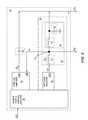
- FIG. 1shows a direct current (DC)-DC converter according to one embodiment of the present disclosure.
- FIG. 2shows the DC-DC converter according to an alternate embodiment of the DC-DC converter.
- FIG. 3shows a radio frequency (RF) communications system according to one embodiment of the present disclosure.
- FIG. 4shows the RF communications system according to an alternate embodiment of the RF communications system.
- FIG. 5shows the RF communications system according to an additional embodiment of the RF communications system.
- FIG. 6shows the RF communications system according to another embodiment of the RF communications system.
- FIG. 1shows a direct current (DC)-DC converter 10 according to one embodiment of the present disclosure.
- the DC-DC converter 10includes a switching supply 12 and a parallel amplifier 14 .
- the switching supply 12includes switching circuitry 16 , a first inductive element L 1 , and a second inductive element L 2 .
- the parallel amplifier 14has a feedback input FBI and a parallel amplifier output PAO.
- the switching circuitry 16has a switching circuitry output SCO.
- the first inductive element L 1is coupled between the switching circuitry output SCO and the feedback input FBI.
- the second inductive element L 2is coupled between the feedback input FBI and the parallel amplifier output PAO.
- the parallel amplifier 14partially provides a first power supply output signal PS 1 via the parallel amplifier output PAO based on a voltage setpoint.
- the switching supply 12partially provides the first power supply output signal PS 1 via the first inductive element L 1 and the second inductive element L 2 .
- the switching supply 12partially provides the first power supply output signal PS 1 via a series combination of the first inductive element L 1 and the second inductive element L 2 .
- the switching supply 12may provide power more efficiently than the parallel amplifier 14 .
- the parallel amplifier 14may provide a voltage of the first power supply output signal PS 1 more accurately than the switching supply 12 .
- the parallel amplifier 14regulates the voltage, called a first voltage V 1 , of the first power supply output signal PS 1 based on the voltage setpoint of the first power supply output signal PS 1 . Further, the switching supply 12 regulates the first power supply output signal PS 1 to minimize an output current, called a parallel amplifier output current IP, from the parallel amplifier 14 to maximize efficiency.
- the parallel amplifier 14behaves like a voltage source and the switching supply 12 behaves like a current source.
- the switching circuitry 16provides a switching output voltage VS and an inductor current IL to the first inductive element L 1 via the switching circuitry output SCO.
- a connection node 18is provided where the first inductive element L 1 and the second inductive element L 2 are connected to one another.
- the connection node 18provides a second voltage V 2 to the parallel amplifier 14 via the feedback input FBI.
- the parallel amplifier 14has a limited open loop gain at high frequencies that are above a frequency threshold. At such frequencies, a group delay in the parallel amplifier 14 may normally limit the ability of the parallel amplifier 14 to accurately regulate the first voltage V 1 of the first power supply output signal PS 1 .
- the parallel amplifier 14partially provides the first power supply output signal PS 1 via the parallel amplifier output PAO based on the voltage setpoint and feeding back a voltage to the feedback input FBI from the connection node 18 between the first inductive element L 1 and the second inductive element L 2 .
- the DC-DC converter 10receives a DC source signal VDC, such that the parallel amplifier 14 partially provides the first power supply output signal PS 1 using the DC source signal VDC and the switching supply 12 partially provides the first power supply output signal PS 1 using the DC source signal VDC.
- FIG. 2shows the DC-DC converter 10 according to an alternate embodiment of the DC-DC converter 10 .
- the DC-DC converter 10 illustrated in FIG. 2is similar to the DC-DC converter 10 illustrated in FIG. 1 , except the DC-DC converter 10 illustrated in FIG. 2 further includes power supply control circuitry 20 and an offset capacitive element CO. Additionally, the switching supply 12 further includes a filter capacitive element CF.
- the power supply control circuitry 20receives the DC source signal VDC and is coupled to the parallel amplifier 14 and the switching circuitry 16 .
- the first inductive element L 1 and the second inductive element L 2provide a second power supply output signal PS 2 via the connection node 18 .
- the offset capacitive element COis coupled between the parallel amplifier output PAO and the second inductive element L 2 , such that the parallel amplifier 14 partially provides the first power supply output signal PS 1 via the parallel amplifier output PAO and the offset capacitive element CO based on the voltage setpoint.
- the offset capacitive element COallows the first voltage V 1 to be higher than a voltage at the parallel amplifier output PAO.
- the parallel amplifier 14may properly regulate the first voltage V 1 even if the first voltage V 1 is greater than a maximum output voltage from the parallel amplifier 14 at the parallel amplifier output PAO.
- the filter capacitive element CFis coupled between the parallel amplifier output PAO and a ground.
- the filter capacitive element CFis coupled between the parallel amplifier output PAO and the ground through the offset capacitive element CO.
- the offset capacitive element COis omitted, such that the filter capacitive element CF is directly coupled between the parallel amplifier output PAO and the ground.
- the first inductive element L 1 , the second inductive element L 2 , and the filter capacitive element CFform a first low-pass filter 22 having a first cutoff frequency.
- the second inductive element L 2 and the filter capacitive element CFform a second low-pass filter 24 having a second cutoff frequency.
- the second cutoff frequencymay be significantly higher than the first cutoff frequency.
- the first low-pass filter 22may be used primarily to filter the switching output voltage VS, which is typically a square wave.
- the second low-pass filter 24may be used to target specific high frequencies, such as certain harmonics of the switching output voltage VS.
- the second cutoff frequencyis at least 10 times greater than the first cutoff frequency. In a second embodiment of the first low-pass filter 22 and the second low-pass filter 24 , the second cutoff frequency is at least 100 times greater than the first cutoff frequency. In a third embodiment of the first low-pass filter 22 and the second low-pass filter 24 , the second cutoff frequency is at least 500 times greater than the first cutoff frequency. In a fourth embodiment of the first low-pass filter 22 and the second low-pass filter 24 , the second cutoff frequency is at least 1000 times greater than the first cutoff frequency.
- the second cutoff frequencyis less than 1000 times greater than the first cutoff frequency. In a sixth embodiment of the first low-pass filter 22 and the second low-pass filter 24 , the second cutoff frequency is less than 5000 times greater than the first cutoff frequency.
- the first inductive element L 1has a first inductance and the second inductive element L 2 has a second inductance.
- a magnitude of the first inductanceis at least 10 times greater than a magnitude of the second inductance.
- a magnitude of the first inductanceis at least 100 times greater than a magnitude of the second inductance.
- a magnitude of the first inductanceis at least 500 times greater than a magnitude of the second inductance.
- a magnitude of the first inductanceis at least 1000 times greater than a magnitude of the second inductance.
- a magnitude of the first inductanceis less than 1000 times greater than a magnitude of the second inductance.
- a magnitude of the first inductanceis less than 5000 times greater than a magnitude of the second inductance.
- FIG. 3shows a radio frequency (RF) communications system 26 according to one embodiment of the present disclosure.
- the RF communications system 26includes RF transmitter circuitry 28 , RF system control circuitry 30 , RF front-end circuitry 32 , an RF antenna 34 , and a DC power source 36 .
- the RF transmitter circuitry 28includes transmitter control circuitry 38 , an RF power amplifier (PA) 40 , the DC-DC converter 10 , and PA bias circuitry 42 .
- the DC-DC converter 10functions as an envelope tracking power supply.
- the DC power source 36is external to the RF communications system 26 .
- the RF front-end circuitry 32receives via the RF antenna 34 , processes, and forwards an RF receive signal RFR to the RF system control circuitry 30 .
- the RF system control circuitry 30provides a power supply control signal VRMP and a transmitter configuration signal PACS to the transmitter control circuitry 38 .
- the RF system control circuitry 30provides an RF input signal RFI to the RF PA 40 .
- the DC power source 36provides a DC source signal VDC to the DC-DC converter 10 .
- the DC power source 36is a battery.
- the power supply control signal VRMPthe power supply control signal VRMP is an envelope power supply control signal.
- the transmitter control circuitry 38is coupled to the DC-DC converter 10 and to the PA bias circuitry 42 .
- the DC-DC converter 10provides the first power supply output signal PS 1 to the RF PA 40 based on the power supply control signal VRMP.
- the first power supply output signal PS 1is a first envelope power supply signal.
- the DC source signal VDCprovides power to the DC-DC converter 10 .
- the first power supply output signal PS 1is based on the DC source signal VDC.
- the power supply control signal VRMPis representative of the voltage setpoint of the first power supply output signal PS 1 .
- the voltage setpointis based on the power supply control signal VRMP.
- the RF PA 40receives and amplifies the RF input signal RFI to provide an RF transmit signal RFT using the first envelope power supply signal, which is the first power supply output signal PS 1 .
- the first envelope power supply signalprovides power for amplification to the RF PA 40 .
- the RF front-end circuitry 32receives, processes, and transmits the RF transmit signal RFT via the RF antenna 34 .
- the transmitter control circuitry 38configures the RF transmitter circuitry 28 based on the transmitter configuration signal PACS.
- the PA bias circuitry 42provides a PA bias signal PAB to the RF PA 40 .
- the PA bias circuitry 42biases the RF PA 40 via the PA bias signal PAB.
- the PA bias circuitry 42biases the RF PA 40 based on the transmitter configuration signal PACS.
- the RF front-end circuitry 32includes at least one RF switch, at least one RF amplifier, at least one RF filter, at least one RF duplexer, at least one RF diplexer, at least one RF amplifier, the like, or any combination thereof.
- the RF system control circuitry 30is RF transceiver circuitry, which may include an RF transceiver IC, baseband controller circuitry, the like, or any combination thereof.
- the first envelope power supply signalprovides power for amplification and envelope tracks the RF transmit signal RFT.
- FIG. 4shows the RF communications system 26 according to an alternate embodiment of the RF communications system 26 .
- the RF communications system 26 illustrated in FIG. 4is similar to the RF communications system 26 illustrated in FIG. 3 , except in the RF communications system 26 illustrated in FIG. 4 , the RF transmitter circuitry 28 further includes a digital communications interface 44 , which is coupled between the transmitter control circuitry 38 and a digital communications bus 46 .
- the digital communications bus 46is also coupled to the RF system control circuitry 30 .
- the RF system control circuitry 30provides the power supply control signal VRMP ( FIG. 3 ) and the transmitter configuration signal PACS ( FIG. 3 ) to the transmitter control circuitry 38 via the digital communications bus 46 and the digital communications interface 44 .
- VRMPFIG. 3
- PACSFIG. 3
- FIG. 5shows details of the DC-DC converter 10 illustrated in FIG. 3 according to one embodiment of the DC-DC converter 10 .
- the DC-DC converter 10includes the power supply control circuitry 20 , the parallel amplifier 14 , and the switching supply 12 .
- the power supply control circuitry 20controls the parallel amplifier 14 and the switching supply 12 .
- the parallel amplifier 14 and the switching supply 12provide the first power supply output signal PS 1 , such that the parallel amplifier 14 partially provides the first power supply output signal PS 1 and the switching supply 12 partially provides the first power supply output signal PS 1 .
- FIG. 6shows the RF communications system 26 according to another embodiment of the RF communications system 26 .
- the RF communications system 26 illustrated in FIG. 6is similar to the RF communications system 26 illustrated in FIG. 3 , except in the RF communications system 26 illustrated in FIG. 6 , the PA bias circuitry 42 ( FIG. 3 ) is omitted and the RF PA 40 includes a driver stage 48 and a final stage 50 , which is coupled to the driver stage 48 .
- the DC-DC converter 10provides the second power supply output signal PS 2 , which is a second envelope power supply signal, to the driver stage 48 based on the power supply control signal VRMP.
- the DC-DC converter 10provides the first power supply output signal PS 1 , which is the first envelope power supply signal, to the final stage 50 based on the power supply control signal VRMP.
- the driver stage 48receives and amplifies the RF input signal RFI to provide a driver stage output signal DSO using the second envelope power supply signal, which provides power for amplification.
- the final stage 50receives and amplifies the driver stage output signal DSO to provide the RF transmit signal RFT using the first envelope power supply signal, which provides power for amplification.
- the first power supply output signal PS 1is fed to a load (not shown) having a load resistance RL, such as the RF PA 40 ( FIG. 3 ).
- the switching output voltage VShas a DC component called a DC voltage VD and a ripple component called an AC voltage VA given by EQ. 1, as shown below.
- VSVD+VA.
- the inductor current ILhas a DC current ID and an AC current IA given by EQ. 2, as shown below.
- ILID+IA.
- the DC-DC converter 10regulates the DC voltage VD to be about equal to the voltage setpoint.
- the first inductive element L 1 and the second inductive element L 2appear approximately as short circuits to the DC component.
- the filter capacitive element CFappears approximately as an open circuit to the DC component. Therefore, the DC voltage VD is approximately applied to the load resistance RL, as intended.
- the first voltage V 1has a first residual ripple voltage VR 1 and the second voltage V 2 has a second residual ripple voltage VR 2 .
- the DC-DC converter 10is the DC-DC converter 10 illustrated in FIG. 2 , such that the second voltage V 2 is fed to the feedback input FBI, as shown.
- the second residual ripple voltage VR 2drives the parallel amplifier 14 to provide a ripple cancellation current, which is the parallel amplifier output current IP.
- the DC-DC converter 10is similar to the DC-DC converter 10 illustrated in FIG. 2 , except the first voltage V 1 is fed to the feedback input FBI instead of the second voltage V 2 , such that the first residual ripple voltage VR 1 drives the parallel amplifier 14 to provide the ripple cancellation current, which is the parallel amplifier output current IP.
- the parallel amplifier 14has a DC open loop gain GO and an open loop bandwidth factor T.
- the parallel amplifier 14has a gain G, as shown in EQ. 5 below.
- GGO /(1 +sT ).
- the open loop bandwidth factor Tis small compared to one, such that the gain G approaches the DC open loop gain GO. Conversely, at frequencies significantly above the open loop bandwidth of the parallel amplifier 14 , the open loop bandwidth factor T is large compared to one, such that the gain G approaches GO/sT.
- the parallel amplifier output current IPis based on the second residual ripple voltage VR 2 , as shown in EQ. 6 below.
- IPG*VR 2 ⁇ ( GO*VR 2)/ sT. EQ. 6:
- the parallel amplifier output current IPis based on the first residual ripple voltage VR 1 , as shown in EQ. 7 below.
- IPG*VR 1 ⁇ ( GO*VR 1)/ sT. EQ. 7:
- EQ. 11is representative of the first approach and EQ. 7 is representative of the second approach.
- the second residual ripple voltage VR 2drives the parallel amplifier 14 and in the second approach, the first residual ripple voltage VR 1 drives the parallel amplifier 14 .
- a smaller first residual ripple voltage VR 1represents better ripple cancellation performance.
- both approachesare assumed to provide the same magnitude of parallel amplifier output current IP.
- the parallel amplifier output current IPis phase-shifted from the first residual ripple voltage VR 1 by about 90 degrees.
- the parallel amplifier output current IPis phase-shifted from the ripple current it is trying to cancel by about 90 degrees, thereby degrading ripple cancellation performance.
- the first approachaccording to EQ.
- the parallel amplifier output current IPhas two terms, namely the (GO)(VR 1 )/sT term and the (GO)(IA)(I 2 )/T term.
- the (GO)(VR 1 )/sT termhas the same phase-alignment shortcoming as in the second approach. But the (GO)(IA)(I 2 )/T term phase-aligns the parallel amplifier output current IP with the ripple current it is trying to cancel. Overall, the phase-alignment in the first approach is improved over the second approach. Additionally, to the extent that the (GO)(VR 1 )/sT term is smaller than the (GO)(IA)(I 2 )/T term, the first residual ripple voltage VR 1 is reduced, thereby improving ripple cancellation.
- circuitrymay use discrete circuitry, integrated circuitry, programmable circuitry, non-volatile circuitry, volatile circuitry, software executing instructions on computing hardware, firmware executing instructions on computing hardware, the like, or any combination thereof.
- the computing hardwaremay include mainframes, micro-processors, micro-controllers, DSPs, the like, or any combination thereof.
Landscapes
- Engineering & Computer Science (AREA)
- Power Engineering (AREA)
- Amplifiers (AREA)
- Dc-Dc Converters (AREA)
Abstract
Description
VS=VD+VA. EQ. 1:
IL=ID+IA. EQ. 2:
ID=VD/RL. EQ. 3:
IA=VA/[s(I1+I2)]. EQ. 4:
G=GO/(1+sT). EQ. 5:
IP=G*VR2≈(GO*VR2)/sT. EQ. 6:
IP=G*VR1≈(GO*VR1)/sT. EQ. 7:
(VR2−VR1)=(s)(IA)(I2), EQ. 8: or
VR2=(s)(IA)(I2)+VR1. EQ. 9:
IP≈(GO)(VR1)/sT+(GO)(s)(IA)(I2)/sT, EQ. 10: or
IP≈(GO)(VR1)/sT+(GO)(IA)(I2)/T. EQ. 11:
Claims (27)
Priority Applications (2)
| Application Number | Priority Date | Filing Date | Title |
|---|---|---|---|
| US13/661,552US8878606B2 (en) | 2011-10-26 | 2012-10-26 | Inductance based parallel amplifier phase compensation |
| US13/782,142US9024688B2 (en) | 2011-10-26 | 2013-03-01 | Dual parallel amplifier based DC-DC converter |
Applications Claiming Priority (3)
| Application Number | Priority Date | Filing Date | Title |
|---|---|---|---|
| US201161551596P | 2011-10-26 | 2011-10-26 | |
| US201161562493P | 2011-11-22 | 2011-11-22 | |
| US13/661,552US8878606B2 (en) | 2011-10-26 | 2012-10-26 | Inductance based parallel amplifier phase compensation |
Related Child Applications (1)
| Application Number | Title | Priority Date | Filing Date |
|---|---|---|---|
| US13/782,142Continuation-In-PartUS9024688B2 (en) | 2011-10-26 | 2013-03-01 | Dual parallel amplifier based DC-DC converter |
Publications (2)
| Publication Number | Publication Date |
|---|---|
| US20130106508A1 US20130106508A1 (en) | 2013-05-02 |
| US8878606B2true US8878606B2 (en) | 2014-11-04 |
Family
ID=47215764
Family Applications (1)
| Application Number | Title | Priority Date | Filing Date |
|---|---|---|---|
| US13/661,552ActiveUS8878606B2 (en) | 2011-10-26 | 2012-10-26 | Inductance based parallel amplifier phase compensation |
Country Status (3)
| Country | Link |
|---|---|
| US (1) | US8878606B2 (en) |
| CN (1) | CN103959189B (en) |
| WO (1) | WO2013063387A2 (en) |
Cited By (29)
| Publication number | Priority date | Publication date | Assignee | Title |
|---|---|---|---|---|
| US9207692B2 (en) | 2012-10-18 | 2015-12-08 | Rf Micro Devices, Inc. | Transitioning from envelope tracking to average power tracking |
| US9225231B2 (en) | 2012-09-14 | 2015-12-29 | Rf Micro Devices, Inc. | Open loop ripple cancellation circuit in a DC-DC converter |
| US9247496B2 (en) | 2011-05-05 | 2016-01-26 | Rf Micro Devices, Inc. | Power loop control based envelope tracking |
| US9246460B2 (en) | 2011-05-05 | 2016-01-26 | Rf Micro Devices, Inc. | Power management architecture for modulated and constant supply operation |
| US9250643B2 (en) | 2011-11-30 | 2016-02-02 | Rf Micro Devices, Inc. | Using a switching signal delay to reduce noise from a switching power supply |
| US9256234B2 (en) | 2011-12-01 | 2016-02-09 | Rf Micro Devices, Inc. | Voltage offset loop for a switching controller |
| US9263996B2 (en) | 2011-07-20 | 2016-02-16 | Rf Micro Devices, Inc. | Quasi iso-gain supply voltage function for envelope tracking systems |
| US9280163B2 (en) | 2011-12-01 | 2016-03-08 | Rf Micro Devices, Inc. | Average power tracking controller |
| US9294041B2 (en) | 2011-10-26 | 2016-03-22 | Rf Micro Devices, Inc. | Average frequency control of switcher for envelope tracking |
| US9300252B2 (en) | 2013-01-24 | 2016-03-29 | Rf Micro Devices, Inc. | Communications based adjustments of a parallel amplifier power supply |
| US9298198B2 (en) | 2011-12-28 | 2016-03-29 | Rf Micro Devices, Inc. | Noise reduction for envelope tracking |
| US9374005B2 (en) | 2013-08-13 | 2016-06-21 | Rf Micro Devices, Inc. | Expanded range DC-DC converter |
| US9379667B2 (en) | 2011-05-05 | 2016-06-28 | Rf Micro Devices, Inc. | Multiple power supply input parallel amplifier based envelope tracking |
| US9377797B2 (en) | 2011-12-01 | 2016-06-28 | Rf Micro Devices, Inc. | Multiple mode RF power converter |
| US9401678B2 (en) | 2010-04-19 | 2016-07-26 | Rf Micro Devices, Inc. | Output impedance compensation of a pseudo-envelope follower power management system |
| US9431974B2 (en) | 2010-04-19 | 2016-08-30 | Qorvo Us, Inc. | Pseudo-envelope following feedback delay compensation |
| US9479118B2 (en) | 2013-04-16 | 2016-10-25 | Rf Micro Devices, Inc. | Dual instantaneous envelope tracking |
| US9484797B2 (en) | 2011-10-26 | 2016-11-01 | Qorvo Us, Inc. | RF switching converter with ripple correction |
| US9494962B2 (en) | 2011-12-02 | 2016-11-15 | Rf Micro Devices, Inc. | Phase reconfigurable switching power supply |
| US9515621B2 (en) | 2011-11-30 | 2016-12-06 | Qorvo Us, Inc. | Multimode RF amplifier system |
| US9614476B2 (en) | 2014-07-01 | 2017-04-04 | Qorvo Us, Inc. | Group delay calibration of RF envelope tracking |
| US9621113B2 (en) | 2010-04-19 | 2017-04-11 | Qorvo Us, Inc. | Pseudo-envelope following power management system |
| US9627975B2 (en) | 2012-11-16 | 2017-04-18 | Qorvo Us, Inc. | Modulated power supply system and method with automatic transition between buck and boost modes |
| US9813036B2 (en) | 2011-12-16 | 2017-11-07 | Qorvo Us, Inc. | Dynamic loadline power amplifier with baseband linearization |
| US9843294B2 (en) | 2015-07-01 | 2017-12-12 | Qorvo Us, Inc. | Dual-mode envelope tracking power converter circuitry |
| US9912297B2 (en) | 2015-07-01 | 2018-03-06 | Qorvo Us, Inc. | Envelope tracking power converter circuitry |
| US9954436B2 (en) | 2010-09-29 | 2018-04-24 | Qorvo Us, Inc. | Single μC-buckboost converter with multiple regulated supply outputs |
| US9973147B2 (en) | 2016-05-10 | 2018-05-15 | Qorvo Us, Inc. | Envelope tracking power management circuit |
| US10476437B2 (en) | 2018-03-15 | 2019-11-12 | Qorvo Us, Inc. | Multimode voltage tracker circuit |
Families Citing this family (1)
| Publication number | Priority date | Publication date | Assignee | Title |
|---|---|---|---|---|
| US10177838B2 (en)* | 2014-09-30 | 2019-01-08 | Skyworks Solutions, Inc. | Shared integrated DC-DC supply regulator |
Citations (226)
| Publication number | Priority date | Publication date | Assignee | Title |
|---|---|---|---|---|
| US3969682A (en) | 1974-10-21 | 1976-07-13 | Oberheim Electronics Inc. | Circuit for dynamic control of phase shift |
| US3980964A (en) | 1974-05-20 | 1976-09-14 | Grodinsky Robert M | Noise reduction circuit |
| US4587552A (en) | 1983-09-02 | 1986-05-06 | Rca Corporation | Apparatus for generating the magnitude of the vector sum of two orthogonal signals as for use in a digital TV receiver |
| US4692889A (en) | 1984-09-28 | 1987-09-08 | Rca Corporation | Circuitry for calculating magnitude of vector sum from its orthogonal components in digital television receiver |
| US4831258A (en) | 1988-03-04 | 1989-05-16 | Exergen Corporation | Dual sensor radiation detector |
| US4996500A (en) | 1989-10-24 | 1991-02-26 | Hewlett-Packard Company | Automatic control system |
| US5099203A (en) | 1990-06-05 | 1992-03-24 | Continental Electronics Corporation | Power amplifier having multiple switched stages and method of operating same |
| US5311309A (en) | 1990-06-01 | 1994-05-10 | Thomson Consumer Electronics, Inc. | Luminance processing system for compressing and expanding video data |
| US5317217A (en) | 1990-11-29 | 1994-05-31 | Deutsche Thomson-Brandt Gmbh | Universal active filter |
| US5351087A (en) | 1990-06-01 | 1994-09-27 | Thomson Consumer Electronics, Inc. | Two stage interpolation system |
| US5414614A (en) | 1994-06-06 | 1995-05-09 | Motorola, Inc. | Dynamically configurable switched capacitor power supply and method |
| US5420643A (en) | 1990-06-01 | 1995-05-30 | Thomson Consumer Electronics, Inc. | Chrominance processing system for compressing and expanding video data |
| US5486871A (en) | 1990-06-01 | 1996-01-23 | Thomson Consumer Electronics, Inc. | Automatic letterbox detection |
| US5532916A (en) | 1992-09-02 | 1996-07-02 | Nec Corporation | Voltage converting circuit and multiphase clock generating circuit used for driving the same |
| US5541547A (en) | 1995-05-03 | 1996-07-30 | Sun Microsystems, Inc. | Test generator system for controllably inducing power pin latch-up and signal pin latch-up in a CMOS device |
| US5581454A (en) | 1994-11-22 | 1996-12-03 | Collins; Hansel | High power switched capacitor voltage conversion and regulation apparatus |
| EP0755121A2 (en) | 1995-07-21 | 1997-01-22 | Nec Corporation | Exponential and logarithmic conversion circuit |
| US5646621A (en) | 1994-11-02 | 1997-07-08 | Advanced Micro Devices, Inc. | Delta-sigma ADC with multi-stage decimation filter and gain compensation filter |
| US5715526A (en) | 1995-09-08 | 1998-02-03 | Qualcomm Incorporated | Apparatus and method for controlling transmission power in a cellular communications system |
| US5767744A (en) | 1995-11-22 | 1998-06-16 | Qsc Audio Products, Inc. | Lightweight fixed frequency discontinuous resonant power supply for audio amplifiers |
| US5822318A (en) | 1994-07-29 | 1998-10-13 | Qualcomm Incorporated | Method and apparatus for controlling power in a variable rate communication system |
| US5898342A (en) | 1998-01-20 | 1999-04-27 | Advanced Micro Devices | Power amplifier arrangement and method for data signal interface |
| US5905407A (en) | 1997-07-30 | 1999-05-18 | Motorola, Inc. | High efficiency power amplifier using combined linear and switching techniques with novel feedback system |
| US5936464A (en) | 1997-11-03 | 1999-08-10 | Motorola, Inc. | Method and apparatus for reducing distortion in a high efficiency power amplifier |
| US6043707A (en) | 1999-01-07 | 2000-03-28 | Motorola, Inc. | Method and apparatus for operating a radio-frequency power amplifier as a variable-class linear amplifier |
| US6043610A (en) | 1998-07-16 | 2000-03-28 | Durel Corporation | Battery operated power supply including a low level boost and a high level boost |
| US6055168A (en) | 1998-03-04 | 2000-04-25 | National Semiconductor Corporation | Capacitor DC-DC converter with PFM and gain hopping |
| US6070181A (en) | 1998-03-27 | 2000-05-30 | Chun-Shan Institute Of Science And Technology | Method and circuit for envelope detection using a peel cone approximation |
| WO2000048306A1 (en) | 1999-02-09 | 2000-08-17 | Tropian, Inc. | High-efficiency amplifier output level and burst control |
| US6118343A (en) | 1999-05-10 | 2000-09-12 | Tyco Electronics Logistics Ag | Power Amplifier incorporating single drain switch and single negative voltage generator |
| US6141541A (en) | 1997-12-31 | 2000-10-31 | Motorola, Inc. | Method, device, phone and base station for providing envelope-following for variable envelope radio frequency signals |
| US6147478A (en) | 1999-09-17 | 2000-11-14 | Texas Instruments Incorporated | Hysteretic regulator and control method having switching frequency independent from output filter |
| US6198645B1 (en) | 1998-07-02 | 2001-03-06 | National Semiconductor Corporation | Buck and boost switched capacitor gain stage with optional shared rest state |
| US6204731B1 (en) | 1998-12-05 | 2001-03-20 | Institute Of Microelectronics | Power amplifier |
| US6256482B1 (en) | 1997-04-07 | 2001-07-03 | Frederick H. Raab | Power- conserving drive-modulation method for envelope-elimination-and-restoration (EER) transmitters |
| US6300826B1 (en) | 2000-05-05 | 2001-10-09 | Ericsson Telefon Ab L M | Apparatus and method for efficiently amplifying wideband envelope signals |
| US6313681B1 (en) | 1998-10-27 | 2001-11-06 | Nec Corporation | Variable delay circuit |
| US6348780B1 (en) | 2000-09-22 | 2002-02-19 | Texas Instruments Incorporated | Frequency control of hysteretic power converter by adjusting hystersis levels |
| US20020071497A1 (en) | 2000-10-31 | 2002-06-13 | Erik Bengtsson | IQ modulation systems and methods that use separate phase and amplitude signal paths and perform modulation within a phase locked loop |
| US6483281B2 (en)* | 2000-02-11 | 2002-11-19 | Champion Microelectronic Corporation | Low power mode and feedback arrangement for a switching power converter |
| US20030031271A1 (en) | 2001-08-07 | 2003-02-13 | Bozeki John Janos | Isolator eliminator for a linear transmitter |
| US20030062950A1 (en) | 2001-09-28 | 2003-04-03 | Kunihiro Hamada | Transmission power controller circuit |
| US6559689B1 (en) | 2000-10-02 | 2003-05-06 | Allegro Microsystems, Inc. | Circuit providing a control voltage to a switch and including a capacitor |
| US6583610B2 (en) | 2001-03-12 | 2003-06-24 | Semtech Corporation | Virtual ripple generation in switch-mode power supplies |
| US20030137286A1 (en) | 2002-01-23 | 2003-07-24 | Donald Kimball | Capacitorless DC-DC converter |
| US6617930B2 (en) | 2000-08-25 | 2003-09-09 | Sharp Kabushiki Kaisha | Power supply circuit for transmitter |
| US6621808B1 (en) | 1999-08-13 | 2003-09-16 | International Business Machines Corporation | Adaptive power control based on a rake receiver configuration in wideband CDMA cellular systems (WCDMA) and methods of operation |
| US6624712B1 (en) | 2002-06-11 | 2003-09-23 | Motorola, Inc. | Method and apparatus for power modulating to prevent instances of clipping |
| US20030198063A1 (en) | 2002-04-18 | 2003-10-23 | Smyth David Bruce | Audio band conducted emissions suppression on power feeders |
| US20030206603A1 (en) | 2002-05-03 | 2003-11-06 | Husted Paul J. | Systems and methods to provide wideband magnitude and phase imbalance calibration and compensation in quadrature receivers |
| US20030220953A1 (en) | 2002-05-17 | 2003-11-27 | Texas Instruments Incorporated | Circuits, systems, and methods implementing approximations for logarithm, inverse logrithm,and reciprocal |
| US6658445B1 (en) | 2000-05-17 | 2003-12-02 | Chun-Shan Institute Of Science And Technology | Apparatus and method for demodulating a square root of the sum of two squares |
| US20030232622A1 (en) | 2002-02-17 | 2003-12-18 | Samsung Electronics Co., Ltd. | Apparatus and method for transmitting and receiving uplink power offset information in a mobile communication system supporting HSDPA |
| WO2004002006A1 (en) | 2002-06-20 | 2003-12-31 | Motorola, Inc. | Method for tuning an envelope tracking amplification system |
| US6681101B1 (en) | 2000-01-11 | 2004-01-20 | Skyworks Solutions, Inc. | RF transmitter with extended efficient power control range |
| US6690652B1 (en) | 1998-10-26 | 2004-02-10 | International Business Machines Corporation | Adaptive power control in wideband CDMA cellular systems (WCDMA) and methods of operation |
| US6701141B2 (en) | 1999-05-18 | 2004-03-02 | Lockheed Martin Corporation | Mixed signal true time delay digital beamformer |
| US6703080B2 (en) | 2002-05-20 | 2004-03-09 | Eni Technology, Inc. | Method and apparatus for VHF plasma processing with load mismatch reliability and stability |
| US20040047329A1 (en) | 2000-09-25 | 2004-03-11 | Huawei Technologies Co., Ltd. | Method for multiple time slot power control |
| US6728163B2 (en) | 2002-08-23 | 2004-04-27 | Micron Technology, Inc. | Controlling a delay lock loop circuit |
| US20040124913A1 (en) | 2002-12-31 | 2004-07-01 | Pallab Midya | Power amplifier circuit and method using bandlimited signal component estimates |
| WO2004082135A2 (en) | 2003-03-12 | 2004-09-23 | Analog Devices, Inc. | Closed loop power control of non-constant envelope waveforms using sample/hold |
| US20040196095A1 (en) | 2002-07-31 | 2004-10-07 | Nec Corporation | Charge pump-type booster circuit |
| US20040219891A1 (en) | 2003-04-30 | 2004-11-04 | Aristotle Hadjichristos | Polar modulation transmitter |
| US6819938B2 (en) | 2001-06-26 | 2004-11-16 | Qualcomm Incorporated | System and method for power control calibration and a wireless communication device |
| US20040239301A1 (en) | 2003-04-16 | 2004-12-02 | Hidenori Kobayashi | Power system |
| EP1492227A1 (en) | 2003-06-24 | 2004-12-29 | Northrop Grumman Corporation | Multi-mode amplifier system |
| US20040267842A1 (en) | 2003-06-24 | 2004-12-30 | Texas Instruments Incorporated | Device with dB-to-linear gain conversion |
| US20050008093A1 (en) | 2003-07-08 | 2005-01-13 | Toru Matsuura | Modulation circuit device, modulation method and radio communication device |
| WO2005013084A2 (en) | 2003-07-31 | 2005-02-10 | Cradle Technologies, Inc. | Method and system for performing operations on data and transferring data |
| US20050032499A1 (en) | 2003-08-08 | 2005-02-10 | Cho Jin Wook | Radio frequency power detecting circuit and method therefor |
| US20050047180A1 (en) | 2003-08-26 | 2005-03-03 | Samsung Electronics Co., Ltd. | Voltage boosting circuit and method |
| US20050064830A1 (en) | 2003-09-16 | 2005-03-24 | Nokia Corporation | Hybrid switched mode/linear power amplifier power supply for use in polar transmitter |
| US20050093630A1 (en) | 2003-10-30 | 2005-05-05 | Whittaker Edward J. | Power level controlling of first amplification stage for an integrated rf power amplifier |
| US20050110562A1 (en) | 2003-11-20 | 2005-05-26 | Ian Robinson | Variable supply amplifier system |
| US20050122171A1 (en) | 2003-12-08 | 2005-06-09 | Osamu Miki | Power source circuit for high frequency power amplifying circuit and semiconductor integrated circuit for power source and electronics component for power source |
| US20050156582A1 (en) | 2004-01-21 | 2005-07-21 | Analog Devices, Inc. | Switched noise filter circuit for a dc-dc converter |
| US20050156662A1 (en) | 2004-01-16 | 2005-07-21 | Arun Raghupathy | Amplifier predistortion and autocalibration method and apparatus |
| US20050157778A1 (en) | 2004-01-15 | 2005-07-21 | Trachewsky Jason A. | Orthogonal normalization for a radio frequency integrated circuit |
| EP1569330A1 (en) | 2004-02-20 | 2005-08-31 | Research In Motion Limited | Method and apparatus for improving power amplifier efficience in wireless communication systems having high peak to average power ratios |
| US20050200407A1 (en) | 2001-12-12 | 2005-09-15 | Renesas Technology Corp. | High frequency power amplifier and wireless communication module |
| US6958596B1 (en) | 2002-12-20 | 2005-10-25 | Intersil Americas Inc. | Compensation sample and hold for voltage regulator amplifier |
| US20060006946A1 (en) | 2004-07-08 | 2006-01-12 | Lawrence Burns | Method and apparatus for an improved power amplifier |
| US6995995B2 (en) | 2003-12-03 | 2006-02-07 | Fairchild Semiconductor Corporation | Digital loop for regulating DC/DC converter with segmented switching |
| WO2006021774A1 (en) | 2004-08-25 | 2006-03-02 | Siemens Aktiengesellschaft | A method of controlling a linear power amplifier |
| US7038536B2 (en) | 2001-08-29 | 2006-05-02 | Tropian, Inc. | Power supply processing for power amplifiers |
| US20060097711A1 (en) | 2004-11-09 | 2006-05-11 | Brandt Randy L | DC-DC converter having magnetic feedback |
| US20060128324A1 (en) | 2004-12-14 | 2006-06-15 | Motorola, Inc. | Amplifier with varying supply voltage and input attenuation based upon supply voltage |
| WO2006073208A1 (en) | 2005-01-06 | 2006-07-13 | Matsushita Electric Industrial Co., Ltd. | Polar modulator and wireless communication apparatus using the same |
| US20060178119A1 (en) | 2005-02-09 | 2006-08-10 | Nokia Corporation | Variable bandwidth envelope modulator for use with envelope elimination and restoration transmitter architecture and method |
| US20060181340A1 (en) | 2005-02-17 | 2006-08-17 | Zywyn Corporation | Regulating charge pump |
| US7099635B2 (en) | 1999-02-09 | 2006-08-29 | Matsushita Electric Industrial Co., Ltd. | High-efficiency modulating RF amplifier |
| US20060220627A1 (en) | 2005-03-29 | 2006-10-05 | Samsung Electronics Co., Ltd. | DC-DC converter utilizing a modified Schmitt trigger circuit and method of modulating a pulse width |
| US20060244513A1 (en) | 2005-04-28 | 2006-11-02 | Chih-Jen Yen | Charge pump |
| US7164893B2 (en) | 2001-08-31 | 2007-01-16 | Motorola, Inc. | Method and apparatus for optimizing supply modulation in a transmitter |
| US20070014382A1 (en) | 2005-07-15 | 2007-01-18 | Nokia Corporation | Reconfigurable transmitter |
| US20070024360A1 (en) | 2005-07-27 | 2007-02-01 | Artesyn Technologies, Inc. | Power supply providing ultrafast modulation of output voltage |
| US7200365B2 (en) | 1998-10-27 | 2007-04-03 | Murata Manufacturing Co., Ltd. | Composite high frequency component and mobile communication device including the same |
| US20070082622A1 (en) | 2004-12-22 | 2007-04-12 | Nokia Corporation | Interoperability improvement between receivers and transmitters in a mobile station |
| US7233130B1 (en) | 2005-08-05 | 2007-06-19 | Rf Micro Devices, Inc. | Active ripple reduction switched mode power supplies |
| US20070146076A1 (en) | 2004-02-06 | 2007-06-28 | Mitsubishi Electric Corporation | Power amplifier unit, communication terminal and control method of power amplifier unit |
| US20070182392A1 (en) | 2006-02-01 | 2007-08-09 | Junji Nishida | DC-DC converter capable of performing for wide and dynamic voltage range |
| US20070183532A1 (en) | 2006-02-06 | 2007-08-09 | Nokia Corporation | Method and system for transmitter envelope delay calibration |
| WO2007107919A1 (en) | 2006-03-17 | 2007-09-27 | Nxp B.V. | Supply circuit with ripple compensation |
| US7279875B2 (en) | 2005-06-16 | 2007-10-09 | Ge Gan | High switching frequency DC-DC converter with fast response time |
| US20070259628A1 (en) | 2006-05-08 | 2007-11-08 | Harris Corporation | Multiband radio with transmitter output power optimization |
| WO2007149346A2 (en) | 2006-06-16 | 2007-12-27 | Pulsewave Rf, Inc. | Radio frequency power amplifier and method using a controlled supply |
| US20080003950A1 (en) | 2006-06-30 | 2008-01-03 | Nokia Corporation | Controlling switching mode power supply of power amplifier |
| US20080044041A1 (en) | 2006-08-21 | 2008-02-21 | John Christopher Tucker | Energy-efficient consumer device audio power output stage |
| US20080081572A1 (en) | 2006-09-29 | 2008-04-03 | Ahmadreza Rofougaran | Method and System for Minimizing Power Consumption in a Communication System |
| US20080104432A1 (en) | 2006-10-30 | 2008-05-01 | Quantance, Inc. | Power combining power supply system |
| US20080150619A1 (en) | 2006-12-22 | 2008-06-26 | Lesso John P | Charge pump circuit and methods of operation thereof |
| US7394233B1 (en)* | 2004-12-02 | 2008-07-01 | Nortel Networks Limited | High efficiency modulated power supply |
| US7405618B2 (en) | 2003-03-04 | 2008-07-29 | Samsung Electronics Co., Ltd. | Method and apparatus for controlling a power amplifier in a mobile communication system |
| US7411316B2 (en) | 2005-02-03 | 2008-08-12 | Richtek Technology Corp. | Dual-input power converter and control methods thereof |
| US20080205095A1 (en) | 2007-02-22 | 2008-08-28 | Stmicroelectronics Sa | Ripple compensator and switching converter having such a ripple compensator |
| US20080242246A1 (en) | 2005-07-27 | 2008-10-02 | Nxp B.V. | Rf Transmitter With Compensation of Differential Path Delay |
| US20080252278A1 (en) | 2006-12-06 | 2008-10-16 | Jonne Jalmar Sebastian Lindeberg | System and Method for Controlling a Hysteretic Mode Converter |
| US20080258831A1 (en) | 2006-01-10 | 2008-10-23 | Nec Corporation | Amplifying apparatus |
| US20080280577A1 (en) | 2006-01-31 | 2008-11-13 | International Business Machines Corporation | Receiver and integrated am-fm/iq demodulators for gigabit-rate data detection |
| US20090004981A1 (en) | 2007-06-27 | 2009-01-01 | Texas Instruments Incorporated | High efficiency digital transmitter incorporating switching power supply and linear power amplifier |
| US7515885B2 (en) | 2001-04-11 | 2009-04-07 | Panasonic Corporation | Communications signal amplifiers having independent power control and amplitude modulation |
| US20090097591A1 (en) | 2007-10-10 | 2009-04-16 | Samsung Electronics Co., Ltd. | Apparatus and method for envelope tracking power amplification in wireless communication system |
| US7529523B1 (en) | 2004-08-23 | 2009-05-05 | Rf Micro Devices, Inc. | N-th order curve fit for power calibration in a mobile terminal |
| US7528807B2 (en) | 2003-07-31 | 2009-05-05 | Lg Electronics Inc. | Power supply and driving method thereof and apparatus and method for driving electro-luminescence display device using the same |
| US20090167260A1 (en) | 2005-06-28 | 2009-07-02 | Manfred Pauritsch | Electrical Power Supply Arrangement and Use Thereof |
| US20090174466A1 (en) | 2008-01-08 | 2009-07-09 | Novatek Microelectronics Corp. | Charge pump circuit |
| US20090184764A1 (en) | 2007-03-13 | 2009-07-23 | Piotr Markowski | Power supply providing ultrafast modulation of output voltage |
| US20090190699A1 (en) | 2002-06-11 | 2009-07-30 | Interdigital Technology Corporation | Gain control method and apparatus |
| US20090218995A1 (en) | 2008-03-03 | 2009-09-03 | Samsung Electronics Co., Ltd. | Apparatus and method for bias modulator using zero current switching |
| US20090230934A1 (en) | 2008-03-12 | 2009-09-17 | Sony Ericsson Mobile Communications Ab | Switched mode voltage converter with low-current mode and methods of performing voltage conversion with low-current mode |
| US7595569B2 (en) | 2004-02-17 | 2009-09-29 | Agere Systems Inc. | Versatile and intelligent power controller |
| US7609114B2 (en) | 2007-09-04 | 2009-10-27 | Upi Semiconductor Corporation | Voltage generating apparatus and methods |
| US7615979B2 (en) | 2005-11-28 | 2009-11-10 | David J. Caldwell | Flexible power converter and simplified process controller |
| US20090289720A1 (en) | 2008-05-23 | 2009-11-26 | Matsushita Electric Industrial Co., Ltd. | High-Efficiency Envelope Tracking Systems and Methods for Radio Frequency Power Amplifiers |
| US7627622B2 (en) | 2003-11-14 | 2009-12-01 | International Business Machines Corporation | System and method of curve fitting |
| US20090319065A1 (en) | 2008-06-19 | 2009-12-24 | Texas Instruments Incorporated | Efficient Asynchronous Sample Rate Conversion |
| US20100001793A1 (en) | 2006-12-12 | 2010-01-07 | Koninklijke Philips Electronics N.V. | High efficiency modulating rf amplifier |
| US7646108B2 (en) | 2006-09-29 | 2010-01-12 | Intel Corporation | Multiple output voltage regulator |
| US20100019840A1 (en) | 2007-01-24 | 2010-01-28 | Kiyohiko Takahashi | Power amplifier |
| GB2462204A (en) | 2008-07-31 | 2010-02-03 | Motorola Inc | Control of Power converters including high-order output filters |
| US20100045247A1 (en) | 2005-04-20 | 2010-02-25 | Nxp B.V. | Parallel arranged linear amplifier and dc-dc converter |
| US7679433B1 (en) | 2007-02-02 | 2010-03-16 | National Semiconductor Corporation | Circuit and method for RF power amplifier power regulation and modulation envelope tracking |
| US7696735B2 (en) | 2007-03-30 | 2010-04-13 | Intel Corporation | Switched capacitor converters |
| US7715811B2 (en) | 2005-03-07 | 2010-05-11 | Andrew Llc | Integrated transceiver with envelope tracking |
| US7724837B2 (en) | 2003-02-20 | 2010-05-25 | Sony Ericsson Mobile Communications Ab | Efficient modulation of RF signals |
| GB2465552A (en) | 2008-11-18 | 2010-05-26 | Nujira Ltd | Tracking power supplies for a multi-stage transmitter amplifier |
| US20100171553A1 (en) | 2008-12-25 | 2010-07-08 | Yoichi Okubo | Power circuit |
| EP2214304A1 (en) | 2009-01-30 | 2010-08-04 | Alcatel-Lucent Deutschland AG | Switch mode assisted linear amplifier for baseband signal amplification |
| US7773691B2 (en) | 2005-04-25 | 2010-08-10 | Rf Micro Devices, Inc. | Power control system for a continuous time mobile transmitter |
| US7777459B2 (en) | 2006-12-30 | 2010-08-17 | Advanced Analogic Technologies, Inc. | High-efficiency DC/DC voltage converter including capacitive switching pre-converter and down inductive switching post-regulator |
| US7783269B2 (en) | 2007-09-20 | 2010-08-24 | Quantance, Inc. | Power amplifier controller with polar transmitter |
| US7782036B1 (en) | 2008-01-07 | 2010-08-24 | National Semiconductor Corporation | Adaptive on-time control for switching regulators |
| US7800427B2 (en) | 2006-11-21 | 2010-09-21 | Samsung Electronics Co., Ltd. | Switched capacitor circuit with inverting amplifier and offset unit |
| US7805115B1 (en) | 2003-06-02 | 2010-09-28 | Analog Devices, Inc. | Variable filter systems and methods for enhanced data rate communication systems |
| US20100253309A1 (en) | 2009-04-06 | 2010-10-07 | Xiaoyu Xi | Accurate current limit for peak current mode dc-dc converter |
| US20100266066A1 (en) | 2007-11-05 | 2010-10-21 | Nec Corporation | Power amplifier and radio wave transmitter having the same |
| EP2244366A1 (en) | 2008-02-08 | 2010-10-27 | Sumitomo Electric Industries, Ltd. | Envelope tracking power supply circuit and high-frequency amplifier including envelope tracking power supply circuit |
| US20100301947A1 (en) | 2006-06-19 | 2010-12-02 | Renesas Technology Corp. | Rf power amplifier |
| US20100308654A1 (en) | 2009-06-09 | 2010-12-09 | Silergy Technology | Mixed mode control for switching regulator with fast transient responses |
| US20100321127A1 (en) | 2008-02-21 | 2010-12-23 | Advantest Corporation | Test apparatus for digital modulated signal |
| US20110018626A1 (en) | 2008-10-24 | 2011-01-27 | Advantest Corporation | Quadrature amplitude demodulator and demodulation method |
| US7880547B2 (en) | 2007-01-10 | 2011-02-01 | Samsung Electro-Mechanics | Systems and methods for power amplifiers with voltage boosting multi-primary transformers |
| US7894216B2 (en) | 2007-05-02 | 2011-02-22 | Cirrus Logic, Inc. | Switching power converter with efficient switching control signal period generation |
| US7898327B2 (en) | 2008-08-29 | 2011-03-01 | Nokia Corporation | Correcting distortions at output of power amplifier |
| US7898268B2 (en) | 2008-02-15 | 2011-03-01 | Infineon Technologies Ag | Circuit and method for capacitor effective series resistance measurement |
| US7907010B2 (en) | 2003-04-07 | 2011-03-15 | Nxp B.V. | Digital amplifier |
| US7915961B1 (en) | 2008-05-13 | 2011-03-29 | National Semiconductor Corporation | Power amplifier multiple stage control for polar modulation circuit |
| US7923974B2 (en) | 2008-01-04 | 2011-04-12 | Chil Semiconductor Corporation | Modification of switch activation order in a power supply |
| US20110084760A1 (en) | 2009-10-09 | 2011-04-14 | Richtek Technology Corp. | Highly efficient class-g amplifier and control method thereof |
| US20110148375A1 (en) | 2009-12-22 | 2011-06-23 | Yamaha Corporation | Power amplifying circuit, DC-DC converter, peak holding circuit, and output voltage control circuit including the peak holding circuit |
| US7994864B2 (en) | 2008-12-15 | 2011-08-09 | Mediatek Inc. | Audio out unit |
| US8000117B2 (en) | 2008-08-13 | 2011-08-16 | Intersil Americas Inc. | Buck boost function based on a capacitor bootstrap input buck converter |
| US8008970B1 (en) | 2010-06-07 | 2011-08-30 | Skyworks Solutions, Inc. | Apparatus and method for enabled switch detection |
| US8022761B2 (en) | 2007-05-18 | 2011-09-20 | Quantance, Inc. | Error driven RF power amplifier control with increased efficiency |
| US8026765B2 (en) | 2009-04-12 | 2011-09-27 | Roberto Michele Giovannotto | Audio frequency amplifier |
| US20110234182A1 (en) | 2008-05-09 | 2011-09-29 | Nujira Limited | Modulated supply stage with feedback to switched supply |
| US20110235827A1 (en) | 2006-06-30 | 2011-09-29 | Lesso John P | Amplifier circuit and methods of operation thereof |
| EP2372904A1 (en) | 2008-12-25 | 2011-10-05 | NEC Corporation | Power amplication device |
| US20110279180A1 (en) | 2009-02-05 | 2011-11-17 | Nec Corporation | Power amplifier and power amplifying method |
| US8068622B2 (en) | 2006-12-13 | 2011-11-29 | Cirrus Logic, Inc. | Method and apparatus for controlling a selectable voltage audio power output stage |
| US20110298539A1 (en) | 2010-06-04 | 2011-12-08 | Quantance, Inc. | Rf power amplifier circuit with mismatch tolerance |
| US8081199B2 (en) | 2009-06-26 | 2011-12-20 | Panasonic Corporation | Light emitting element drive apparatus, planar illumination apparatus, and liquid crystal display apparatus |
| US8093951B1 (en) | 2009-04-14 | 2012-01-10 | Cirrus Logic, Inc. | Pulse-width modulated (PWM) audio power amplifier having output signal magnitude controlled pulse voltage and switching frequency |
| US20120025907A1 (en) | 2010-07-28 | 2012-02-02 | Korea Advanced Institute Of Science And Technology | Power amplifier |
| US20120025919A1 (en) | 2010-07-28 | 2012-02-02 | Active-Semi, Inc. | Synchronization of multiple high frequency switching power converters in an integrated circuit |
| US20120034893A1 (en) | 2010-02-01 | 2012-02-09 | Rf Micro Devices, Inc. | Envelope power supply calibration of a multi-mode radio frequency power amplifier |
| US20120049953A1 (en) | 2010-08-25 | 2012-03-01 | Rf Micro Devices, Inc. | Multi-mode/multi-band power management system |
| US8159297B2 (en) | 2009-06-26 | 2012-04-17 | Fujitsu Limited | Transmission device, distortion compensation device, and distortion compensation method |
| GB2484475A (en) | 2010-10-11 | 2012-04-18 | Toshiba Res Europ Ltd | A power supply modulator for an RF amplifier, using a current-output class G amplifier |
| US8164388B2 (en) | 2009-09-18 | 2012-04-24 | Yamaha Corporation | Amplifying apparatus |
| US8174313B2 (en) | 2010-05-17 | 2012-05-08 | Avago Technologies Wireless Ip (Singapore) Pte. Ltd. | Apparatus and method for controlling power amplifier |
| US8183929B2 (en) | 2010-04-09 | 2012-05-22 | Viasat, Inc. | Multi-chip doherty amplifier with integrated power detection |
| US20120133299A1 (en) | 2010-11-30 | 2012-05-31 | Infineon Technologies Ag | Multi Channel LED Driver |
| US20120139516A1 (en) | 2010-12-02 | 2012-06-07 | Richtek Technology Corporation, R.O.C. | Power supply circuit with adaptive input selection and method for power supply |
| US8198941B2 (en) | 2007-08-03 | 2012-06-12 | Wolfson Microelectronics Plc | Amplifier circuit and method of amplifying a signal in an amplifier circuit |
| US8204456B2 (en) | 2010-09-15 | 2012-06-19 | Fujitsu Semiconductor Limited | Systems and methods for spurious emission cancellation |
| US20120154035A1 (en) | 2010-12-21 | 2012-06-21 | Fujitsu Limited | Amplifying device |
| US20120154054A1 (en) | 2010-12-17 | 2012-06-21 | Skyworks Solutions, Inc. | Apparatus and methods for oscillation suppression |
| US20120170334A1 (en) | 2011-01-03 | 2012-07-05 | Paolo Menegoli | Hysteretic CL power converter |
| US20120176196A1 (en) | 2011-01-10 | 2012-07-12 | Rf Micro Devices, Inc. | Power management system for multi-carriers transmitter |
| US20120194274A1 (en) | 2011-02-01 | 2012-08-02 | Paul Fowers | Integrated circuit, wireless communication unit and method for providing a power supply |
| US20120200354A1 (en) | 2011-02-07 | 2012-08-09 | Nujira Ltd | Apparatus and methods for envelope tracking calibration |
| US20120236444A1 (en) | 2011-03-14 | 2012-09-20 | Qualcomm Incorporated | Charge pump electrostatic discharge protection |
| US8289084B2 (en) | 2010-06-07 | 2012-10-16 | Renesas Electronics Corporation | RF power amplifier device and operating method thereof |
| US20120299647A1 (en) | 2010-04-20 | 2012-11-29 | Rf Micro Devices, Inc. | Pa envelope power supply undershoot compensation |
| WO2012172544A1 (en) | 2011-06-16 | 2012-12-20 | Fleischer David Leonardo | Method and system for boosting the supply of power amplifier |
| US8362837B2 (en) | 2011-05-23 | 2013-01-29 | Vyycore Ltd. | System and a method for amplifying a signal by multiple non-linear power amplifiers |
| US20130034139A1 (en) | 2011-02-07 | 2013-02-07 | Rf Micro Devices, Inc. | Group delay calibration method for power amplifier envelope tracking |
| US20130094553A1 (en) | 2011-10-14 | 2013-04-18 | Samsung Electronics Co. Ltd. | Apparatus and method for calibration of supply modulation in transmitter |
| US20130169245A1 (en) | 2011-12-28 | 2013-07-04 | Rf Micro Devices, Inc. | Noise reduction for envelope tracking |
| US20130229235A1 (en) | 2010-11-17 | 2013-09-05 | Masami Ohnishi | High-frequency amplifier, and high-frequency module and wireless transceiver using same |
| US8541993B2 (en) | 2009-07-22 | 2013-09-24 | Wolfson Microelectronics Plc | DC-DC converters operable in a discontinuous switching mode |
| US8542061B2 (en) | 2010-04-20 | 2013-09-24 | Rf Micro Devices, Inc. | Charge pump based power amplifier envelope power supply and bias power supply |
| US8558616B2 (en) | 2010-11-22 | 2013-10-15 | Fujitsu Limited | Amplifying apparatus |
| US20130307617A1 (en) | 2010-04-19 | 2013-11-21 | Rf Micro Devices, Inc. | Pseudo-envelope following power management system |
| US20130328613A1 (en) | 2012-06-11 | 2013-12-12 | Rf Micro Devices, Inc. | Power source multiplexer |
| US8611402B2 (en) | 2011-02-02 | 2013-12-17 | Rf Micro Devices, Inc. | Fast envelope system calibration |
| US8618868B2 (en) | 2011-08-17 | 2013-12-31 | Rf Micro Devices, Inc. | Single charge-pump buck-boost for providing independent voltages |
| US8626091B2 (en) | 2011-07-15 | 2014-01-07 | Rf Micro Devices, Inc. | Envelope tracking with variable compression |
| US8624760B2 (en) | 2011-02-07 | 2014-01-07 | Rf Micro Devices, Inc. | Apparatuses and methods for rate conversion and fractional delay calculation using a coefficient look up table |
| US20140009227A1 (en) | 2010-04-19 | 2014-01-09 | Rf Micro Devices, Inc. | Output impedance compensation of a pseudo-envelope follower power management system |
| US20140009200A1 (en) | 2010-04-19 | 2014-01-09 | Rf Micro Devices, Inc. | Programmable delay circuitry |
| US8638165B2 (en) | 2011-06-06 | 2014-01-28 | Qualcomm Incorporated | Switched-capacitor DC blocking amplifier |
| US8648657B1 (en) | 2012-08-13 | 2014-02-11 | Broadcom Corporation | Mobile device including a power amplifier with selectable voltage supply |
| US8718582B2 (en) | 2008-02-08 | 2014-05-06 | Qualcomm Incorporated | Multi-mode power amplifiers |
Family Cites Families (1)
| Publication number | Priority date | Publication date | Assignee | Title |
|---|---|---|---|---|
| CN201674399U (en)* | 2010-05-14 | 2010-12-15 | 珠海世纪鼎利通信科技股份有限公司 | A low ripple power supply device |
- 2012
- 2012-10-26CNCN201280052694.2Apatent/CN103959189B/enactiveActive
- 2012-10-26WOPCT/US2012/062110patent/WO2013063387A2/enactiveApplication Filing
- 2012-10-26USUS13/661,552patent/US8878606B2/enactiveActive
Patent Citations (240)
| Publication number | Priority date | Publication date | Assignee | Title |
|---|---|---|---|---|
| US3980964A (en) | 1974-05-20 | 1976-09-14 | Grodinsky Robert M | Noise reduction circuit |
| US3969682A (en) | 1974-10-21 | 1976-07-13 | Oberheim Electronics Inc. | Circuit for dynamic control of phase shift |
| US4587552A (en) | 1983-09-02 | 1986-05-06 | Rca Corporation | Apparatus for generating the magnitude of the vector sum of two orthogonal signals as for use in a digital TV receiver |
| US4692889A (en) | 1984-09-28 | 1987-09-08 | Rca Corporation | Circuitry for calculating magnitude of vector sum from its orthogonal components in digital television receiver |
| US4831258A (en) | 1988-03-04 | 1989-05-16 | Exergen Corporation | Dual sensor radiation detector |
| US4996500A (en) | 1989-10-24 | 1991-02-26 | Hewlett-Packard Company | Automatic control system |
| US5351087A (en) | 1990-06-01 | 1994-09-27 | Thomson Consumer Electronics, Inc. | Two stage interpolation system |
| US5311309A (en) | 1990-06-01 | 1994-05-10 | Thomson Consumer Electronics, Inc. | Luminance processing system for compressing and expanding video data |
| US5420643A (en) | 1990-06-01 | 1995-05-30 | Thomson Consumer Electronics, Inc. | Chrominance processing system for compressing and expanding video data |
| US5486871A (en) | 1990-06-01 | 1996-01-23 | Thomson Consumer Electronics, Inc. | Automatic letterbox detection |
| US5099203A (en) | 1990-06-05 | 1992-03-24 | Continental Electronics Corporation | Power amplifier having multiple switched stages and method of operating same |
| US5317217A (en) | 1990-11-29 | 1994-05-31 | Deutsche Thomson-Brandt Gmbh | Universal active filter |
| US5532916A (en) | 1992-09-02 | 1996-07-02 | Nec Corporation | Voltage converting circuit and multiphase clock generating circuit used for driving the same |
| US5414614A (en) | 1994-06-06 | 1995-05-09 | Motorola, Inc. | Dynamically configurable switched capacitor power supply and method |
| US5822318A (en) | 1994-07-29 | 1998-10-13 | Qualcomm Incorporated | Method and apparatus for controlling power in a variable rate communication system |
| US5646621A (en) | 1994-11-02 | 1997-07-08 | Advanced Micro Devices, Inc. | Delta-sigma ADC with multi-stage decimation filter and gain compensation filter |
| US5581454A (en) | 1994-11-22 | 1996-12-03 | Collins; Hansel | High power switched capacitor voltage conversion and regulation apparatus |
| US5541547A (en) | 1995-05-03 | 1996-07-30 | Sun Microsystems, Inc. | Test generator system for controllably inducing power pin latch-up and signal pin latch-up in a CMOS device |
| EP0755121A2 (en) | 1995-07-21 | 1997-01-22 | Nec Corporation | Exponential and logarithmic conversion circuit |
| US5715526A (en) | 1995-09-08 | 1998-02-03 | Qualcomm Incorporated | Apparatus and method for controlling transmission power in a cellular communications system |
| US5767744A (en) | 1995-11-22 | 1998-06-16 | Qsc Audio Products, Inc. | Lightweight fixed frequency discontinuous resonant power supply for audio amplifiers |
| US6256482B1 (en) | 1997-04-07 | 2001-07-03 | Frederick H. Raab | Power- conserving drive-modulation method for envelope-elimination-and-restoration (EER) transmitters |
| US5905407A (en) | 1997-07-30 | 1999-05-18 | Motorola, Inc. | High efficiency power amplifier using combined linear and switching techniques with novel feedback system |
| US5936464A (en) | 1997-11-03 | 1999-08-10 | Motorola, Inc. | Method and apparatus for reducing distortion in a high efficiency power amplifier |
| US6141541A (en) | 1997-12-31 | 2000-10-31 | Motorola, Inc. | Method, device, phone and base station for providing envelope-following for variable envelope radio frequency signals |
| US5898342A (en) | 1998-01-20 | 1999-04-27 | Advanced Micro Devices | Power amplifier arrangement and method for data signal interface |
| US6055168A (en) | 1998-03-04 | 2000-04-25 | National Semiconductor Corporation | Capacitor DC-DC converter with PFM and gain hopping |
| US6070181A (en) | 1998-03-27 | 2000-05-30 | Chun-Shan Institute Of Science And Technology | Method and circuit for envelope detection using a peel cone approximation |
| US6198645B1 (en) | 1998-07-02 | 2001-03-06 | National Semiconductor Corporation | Buck and boost switched capacitor gain stage with optional shared rest state |
| US6043610A (en) | 1998-07-16 | 2000-03-28 | Durel Corporation | Battery operated power supply including a low level boost and a high level boost |
| US6690652B1 (en) | 1998-10-26 | 2004-02-10 | International Business Machines Corporation | Adaptive power control in wideband CDMA cellular systems (WCDMA) and methods of operation |
| US6313681B1 (en) | 1998-10-27 | 2001-11-06 | Nec Corporation | Variable delay circuit |
| US7200365B2 (en) | 1998-10-27 | 2007-04-03 | Murata Manufacturing Co., Ltd. | Composite high frequency component and mobile communication device including the same |
| US6204731B1 (en) | 1998-12-05 | 2001-03-20 | Institute Of Microelectronics | Power amplifier |
| US6043707A (en) | 1999-01-07 | 2000-03-28 | Motorola, Inc. | Method and apparatus for operating a radio-frequency power amplifier as a variable-class linear amplifier |
| US7099635B2 (en) | 1999-02-09 | 2006-08-29 | Matsushita Electric Industrial Co., Ltd. | High-efficiency modulating RF amplifier |
| WO2000048306A1 (en) | 1999-02-09 | 2000-08-17 | Tropian, Inc. | High-efficiency amplifier output level and burst control |
| US6118343A (en) | 1999-05-10 | 2000-09-12 | Tyco Electronics Logistics Ag | Power Amplifier incorporating single drain switch and single negative voltage generator |
| US6701141B2 (en) | 1999-05-18 | 2004-03-02 | Lockheed Martin Corporation | Mixed signal true time delay digital beamformer |
| US6621808B1 (en) | 1999-08-13 | 2003-09-16 | International Business Machines Corporation | Adaptive power control based on a rake receiver configuration in wideband CDMA cellular systems (WCDMA) and methods of operation |
| US6147478A (en) | 1999-09-17 | 2000-11-14 | Texas Instruments Incorporated | Hysteretic regulator and control method having switching frequency independent from output filter |
| US6681101B1 (en) | 2000-01-11 | 2004-01-20 | Skyworks Solutions, Inc. | RF transmitter with extended efficient power control range |
| US6483281B2 (en)* | 2000-02-11 | 2002-11-19 | Champion Microelectronic Corporation | Low power mode and feedback arrangement for a switching power converter |
| US6300826B1 (en) | 2000-05-05 | 2001-10-09 | Ericsson Telefon Ab L M | Apparatus and method for efficiently amplifying wideband envelope signals |
| US6658445B1 (en) | 2000-05-17 | 2003-12-02 | Chun-Shan Institute Of Science And Technology | Apparatus and method for demodulating a square root of the sum of two squares |
| US6617930B2 (en) | 2000-08-25 | 2003-09-09 | Sharp Kabushiki Kaisha | Power supply circuit for transmitter |
| US6348780B1 (en) | 2000-09-22 | 2002-02-19 | Texas Instruments Incorporated | Frequency control of hysteretic power converter by adjusting hystersis levels |
| US20040047329A1 (en) | 2000-09-25 | 2004-03-11 | Huawei Technologies Co., Ltd. | Method for multiple time slot power control |
| US6559689B1 (en) | 2000-10-02 | 2003-05-06 | Allegro Microsystems, Inc. | Circuit providing a control voltage to a switch and including a capacitor |
| US20020071497A1 (en) | 2000-10-31 | 2002-06-13 | Erik Bengtsson | IQ modulation systems and methods that use separate phase and amplitude signal paths and perform modulation within a phase locked loop |
| US6583610B2 (en) | 2001-03-12 | 2003-06-24 | Semtech Corporation | Virtual ripple generation in switch-mode power supplies |
| US7515885B2 (en) | 2001-04-11 | 2009-04-07 | Panasonic Corporation | Communications signal amplifiers having independent power control and amplitude modulation |
| US6819938B2 (en) | 2001-06-26 | 2004-11-16 | Qualcomm Incorporated | System and method for power control calibration and a wireless communication device |
| US20030031271A1 (en) | 2001-08-07 | 2003-02-13 | Bozeki John Janos | Isolator eliminator for a linear transmitter |
| US7038536B2 (en) | 2001-08-29 | 2006-05-02 | Tropian, Inc. | Power supply processing for power amplifiers |
| US7164893B2 (en) | 2001-08-31 | 2007-01-16 | Motorola, Inc. | Method and apparatus for optimizing supply modulation in a transmitter |
| US20030062950A1 (en) | 2001-09-28 | 2003-04-03 | Kunihiro Hamada | Transmission power controller circuit |
| US20050200407A1 (en) | 2001-12-12 | 2005-09-15 | Renesas Technology Corp. | High frequency power amplifier and wireless communication module |
| US20030137286A1 (en) | 2002-01-23 | 2003-07-24 | Donald Kimball | Capacitorless DC-DC converter |
| US20030232622A1 (en) | 2002-02-17 | 2003-12-18 | Samsung Electronics Co., Ltd. | Apparatus and method for transmitting and receiving uplink power offset information in a mobile communication system supporting HSDPA |
| US20030198063A1 (en) | 2002-04-18 | 2003-10-23 | Smyth David Bruce | Audio band conducted emissions suppression on power feeders |
| US20030206603A1 (en) | 2002-05-03 | 2003-11-06 | Husted Paul J. | Systems and methods to provide wideband magnitude and phase imbalance calibration and compensation in quadrature receivers |
| US20030220953A1 (en) | 2002-05-17 | 2003-11-27 | Texas Instruments Incorporated | Circuits, systems, and methods implementing approximations for logarithm, inverse logrithm,and reciprocal |
| US6703080B2 (en) | 2002-05-20 | 2004-03-09 | Eni Technology, Inc. | Method and apparatus for VHF plasma processing with load mismatch reliability and stability |
| US20090190699A1 (en) | 2002-06-11 | 2009-07-30 | Interdigital Technology Corporation | Gain control method and apparatus |
| US6624712B1 (en) | 2002-06-11 | 2003-09-23 | Motorola, Inc. | Method and apparatus for power modulating to prevent instances of clipping |
| WO2004002006A1 (en) | 2002-06-20 | 2003-12-31 | Motorola, Inc. | Method for tuning an envelope tracking amplification system |
| US20040196095A1 (en) | 2002-07-31 | 2004-10-07 | Nec Corporation | Charge pump-type booster circuit |
| US6728163B2 (en) | 2002-08-23 | 2004-04-27 | Micron Technology, Inc. | Controlling a delay lock loop circuit |
| US6958596B1 (en) | 2002-12-20 | 2005-10-25 | Intersil Americas Inc. | Compensation sample and hold for voltage regulator amplifier |
| US20040124913A1 (en) | 2002-12-31 | 2004-07-01 | Pallab Midya | Power amplifier circuit and method using bandlimited signal component estimates |
| US7724837B2 (en) | 2003-02-20 | 2010-05-25 | Sony Ericsson Mobile Communications Ab | Efficient modulation of RF signals |
| US7405618B2 (en) | 2003-03-04 | 2008-07-29 | Samsung Electronics Co., Ltd. | Method and apparatus for controlling a power amplifier in a mobile communication system |
| WO2004082135A2 (en) | 2003-03-12 | 2004-09-23 | Analog Devices, Inc. | Closed loop power control of non-constant envelope waveforms using sample/hold |
| US7907010B2 (en) | 2003-04-07 | 2011-03-15 | Nxp B.V. | Digital amplifier |
| US20040239301A1 (en) | 2003-04-16 | 2004-12-02 | Hidenori Kobayashi | Power system |
| US20040219891A1 (en) | 2003-04-30 | 2004-11-04 | Aristotle Hadjichristos | Polar modulation transmitter |
| US7805115B1 (en) | 2003-06-02 | 2010-09-28 | Analog Devices, Inc. | Variable filter systems and methods for enhanced data rate communication systems |
| EP1492227A1 (en) | 2003-06-24 | 2004-12-29 | Northrop Grumman Corporation | Multi-mode amplifier system |
| US7043213B2 (en) | 2003-06-24 | 2006-05-09 | Northrop Grumman Corporation | Multi-mode amplifier system |
| US20040267842A1 (en) | 2003-06-24 | 2004-12-30 | Texas Instruments Incorporated | Device with dB-to-linear gain conversion |
| US20040266366A1 (en) | 2003-06-24 | 2004-12-30 | Ian Robinson | Multi-mode amplifier system |
| US20050008093A1 (en) | 2003-07-08 | 2005-01-13 | Toru Matsuura | Modulation circuit device, modulation method and radio communication device |
| US7528807B2 (en) | 2003-07-31 | 2009-05-05 | Lg Electronics Inc. | Power supply and driving method thereof and apparatus and method for driving electro-luminescence display device using the same |
| WO2005013084A2 (en) | 2003-07-31 | 2005-02-10 | Cradle Technologies, Inc. | Method and system for performing operations on data and transferring data |
| US20050032499A1 (en) | 2003-08-08 | 2005-02-10 | Cho Jin Wook | Radio frequency power detecting circuit and method therefor |
| US20050047180A1 (en) | 2003-08-26 | 2005-03-03 | Samsung Electronics Co., Ltd. | Voltage boosting circuit and method |
| US7058373B2 (en) | 2003-09-16 | 2006-06-06 | Nokia Corporation | Hybrid switched mode/linear power amplifier power supply for use in polar transmitter |
| US7653366B2 (en) | 2003-09-16 | 2010-01-26 | Nokia Corporation | Hybrid switched mode/linear power amplifier power supply for use in polar transmitter |
| US20050064830A1 (en) | 2003-09-16 | 2005-03-24 | Nokia Corporation | Hybrid switched mode/linear power amplifier power supply for use in polar transmitter |
| US20050093630A1 (en) | 2003-10-30 | 2005-05-05 | Whittaker Edward J. | Power level controlling of first amplification stage for an integrated rf power amplifier |
| US7627622B2 (en) | 2003-11-14 | 2009-12-01 | International Business Machines Corporation | System and method of curve fitting |
| US20050110562A1 (en) | 2003-11-20 | 2005-05-26 | Ian Robinson | Variable supply amplifier system |
| US6995995B2 (en) | 2003-12-03 | 2006-02-07 | Fairchild Semiconductor Corporation | Digital loop for regulating DC/DC converter with segmented switching |
| US20050122171A1 (en) | 2003-12-08 | 2005-06-09 | Osamu Miki | Power source circuit for high frequency power amplifying circuit and semiconductor integrated circuit for power source and electronics component for power source |
| US20050157778A1 (en) | 2004-01-15 | 2005-07-21 | Trachewsky Jason A. | Orthogonal normalization for a radio frequency integrated circuit |
| US20050156662A1 (en) | 2004-01-16 | 2005-07-21 | Arun Raghupathy | Amplifier predistortion and autocalibration method and apparatus |
| US20050156582A1 (en) | 2004-01-21 | 2005-07-21 | Analog Devices, Inc. | Switched noise filter circuit for a dc-dc converter |
| US20070146076A1 (en) | 2004-02-06 | 2007-06-28 | Mitsubishi Electric Corporation | Power amplifier unit, communication terminal and control method of power amplifier unit |
| US7595569B2 (en) | 2004-02-17 | 2009-09-29 | Agere Systems Inc. | Versatile and intelligent power controller |
| EP1569330A1 (en) | 2004-02-20 | 2005-08-31 | Research In Motion Limited | Method and apparatus for improving power amplifier efficience in wireless communication systems having high peak to average power ratios |
| US20060006946A1 (en) | 2004-07-08 | 2006-01-12 | Lawrence Burns | Method and apparatus for an improved power amplifier |
| US7529523B1 (en) | 2004-08-23 | 2009-05-05 | Rf Micro Devices, Inc. | N-th order curve fit for power calibration in a mobile terminal |
| WO2006021774A1 (en) | 2004-08-25 | 2006-03-02 | Siemens Aktiengesellschaft | A method of controlling a linear power amplifier |
| US20060097711A1 (en) | 2004-11-09 | 2006-05-11 | Brandt Randy L | DC-DC converter having magnetic feedback |
| US7394233B1 (en)* | 2004-12-02 | 2008-07-01 | Nortel Networks Limited | High efficiency modulated power supply |
| US20060128324A1 (en) | 2004-12-14 | 2006-06-15 | Motorola, Inc. | Amplifier with varying supply voltage and input attenuation based upon supply voltage |
| US7539466B2 (en) | 2004-12-14 | 2009-05-26 | Motorola, Inc. | Amplifier with varying supply voltage and input attenuation based upon supply voltage |
| US20070082622A1 (en) | 2004-12-22 | 2007-04-12 | Nokia Corporation | Interoperability improvement between receivers and transmitters in a mobile station |
| WO2006073208A1 (en) | 2005-01-06 | 2006-07-13 | Matsushita Electric Industrial Co., Ltd. | Polar modulator and wireless communication apparatus using the same |
| US7411316B2 (en) | 2005-02-03 | 2008-08-12 | Richtek Technology Corp. | Dual-input power converter and control methods thereof |
| US20060178119A1 (en) | 2005-02-09 | 2006-08-10 | Nokia Corporation | Variable bandwidth envelope modulator for use with envelope elimination and restoration transmitter architecture and method |
| US20060181340A1 (en) | 2005-02-17 | 2006-08-17 | Zywyn Corporation | Regulating charge pump |
| US7715811B2 (en) | 2005-03-07 | 2010-05-11 | Andrew Llc | Integrated transceiver with envelope tracking |
| US20060220627A1 (en) | 2005-03-29 | 2006-10-05 | Samsung Electronics Co., Ltd. | DC-DC converter utilizing a modified Schmitt trigger circuit and method of modulating a pulse width |
| US20100045247A1 (en) | 2005-04-20 | 2010-02-25 | Nxp B.V. | Parallel arranged linear amplifier and dc-dc converter |
| US7773691B2 (en) | 2005-04-25 | 2010-08-10 | Rf Micro Devices, Inc. | Power control system for a continuous time mobile transmitter |
| US20060244513A1 (en) | 2005-04-28 | 2006-11-02 | Chih-Jen Yen | Charge pump |
| US7279875B2 (en) | 2005-06-16 | 2007-10-09 | Ge Gan | High switching frequency DC-DC converter with fast response time |
| US20090167260A1 (en) | 2005-06-28 | 2009-07-02 | Manfred Pauritsch | Electrical Power Supply Arrangement and Use Thereof |
| US20070014382A1 (en) | 2005-07-15 | 2007-01-18 | Nokia Corporation | Reconfigurable transmitter |
| US20080242246A1 (en) | 2005-07-27 | 2008-10-02 | Nxp B.V. | Rf Transmitter With Compensation of Differential Path Delay |
| US20070024360A1 (en) | 2005-07-27 | 2007-02-01 | Artesyn Technologies, Inc. | Power supply providing ultrafast modulation of output voltage |
| US7233130B1 (en) | 2005-08-05 | 2007-06-19 | Rf Micro Devices, Inc. | Active ripple reduction switched mode power supplies |
| US7615979B2 (en) | 2005-11-28 | 2009-11-10 | David J. Caldwell | Flexible power converter and simplified process controller |
| US20080258831A1 (en) | 2006-01-10 | 2008-10-23 | Nec Corporation | Amplifying apparatus |
| US20080280577A1 (en) | 2006-01-31 | 2008-11-13 | International Business Machines Corporation | Receiver and integrated am-fm/iq demodulators for gigabit-rate data detection |
| US20070182392A1 (en) | 2006-02-01 | 2007-08-09 | Junji Nishida | DC-DC converter capable of performing for wide and dynamic voltage range |
| US20070183532A1 (en) | 2006-02-06 | 2007-08-09 | Nokia Corporation | Method and system for transmitter envelope delay calibration |
| WO2007107919A1 (en) | 2006-03-17 | 2007-09-27 | Nxp B.V. | Supply circuit with ripple compensation |
| US20070259628A1 (en) | 2006-05-08 | 2007-11-08 | Harris Corporation | Multiband radio with transmitter output power optimization |
| WO2007149346A2 (en) | 2006-06-16 | 2007-12-27 | Pulsewave Rf, Inc. | Radio frequency power amplifier and method using a controlled supply |
| US20100301947A1 (en) | 2006-06-19 | 2010-12-02 | Renesas Technology Corp. | Rf power amplifier |
| US20110235827A1 (en) | 2006-06-30 | 2011-09-29 | Lesso John P | Amplifier circuit and methods of operation thereof |
| US20080003950A1 (en) | 2006-06-30 | 2008-01-03 | Nokia Corporation | Controlling switching mode power supply of power amplifier |
| US20080044041A1 (en) | 2006-08-21 | 2008-02-21 | John Christopher Tucker | Energy-efficient consumer device audio power output stage |
| US7646108B2 (en) | 2006-09-29 | 2010-01-12 | Intel Corporation | Multiple output voltage regulator |
| US20080081572A1 (en) | 2006-09-29 | 2008-04-03 | Ahmadreza Rofougaran | Method and System for Minimizing Power Consumption in a Communication System |
| US20080104432A1 (en) | 2006-10-30 | 2008-05-01 | Quantance, Inc. | Power combining power supply system |
| US7800427B2 (en) | 2006-11-21 | 2010-09-21 | Samsung Electronics Co., Ltd. | Switched capacitor circuit with inverting amplifier and offset unit |
| US20080252278A1 (en) | 2006-12-06 | 2008-10-16 | Jonne Jalmar Sebastian Lindeberg | System and Method for Controlling a Hysteretic Mode Converter |
| US20100001793A1 (en) | 2006-12-12 | 2010-01-07 | Koninklijke Philips Electronics N.V. | High efficiency modulating rf amplifier |
| US8068622B2 (en) | 2006-12-13 | 2011-11-29 | Cirrus Logic, Inc. | Method and apparatus for controlling a selectable voltage audio power output stage |
| US20080150619A1 (en) | 2006-12-22 | 2008-06-26 | Lesso John P | Charge pump circuit and methods of operation thereof |
| US7777459B2 (en) | 2006-12-30 | 2010-08-17 | Advanced Analogic Technologies, Inc. | High-efficiency DC/DC voltage converter including capacitive switching pre-converter and down inductive switching post-regulator |
| US7880547B2 (en) | 2007-01-10 | 2011-02-01 | Samsung Electro-Mechanics | Systems and methods for power amplifiers with voltage boosting multi-primary transformers |
| US7965140B2 (en) | 2007-01-24 | 2011-06-21 | Nec Corporation | Power amplifier |
| US20100019840A1 (en) | 2007-01-24 | 2010-01-28 | Kiyohiko Takahashi | Power amplifier |
| US7679433B1 (en) | 2007-02-02 | 2010-03-16 | National Semiconductor Corporation | Circuit and method for RF power amplifier power regulation and modulation envelope tracking |
| US20080205095A1 (en) | 2007-02-22 | 2008-08-28 | Stmicroelectronics Sa | Ripple compensator and switching converter having such a ripple compensator |
| US7859336B2 (en) | 2007-03-13 | 2010-12-28 | Astec International Limited | Power supply providing ultrafast modulation of output voltage |
| US20090184764A1 (en) | 2007-03-13 | 2009-07-23 | Piotr Markowski | Power supply providing ultrafast modulation of output voltage |
| US7696735B2 (en) | 2007-03-30 | 2010-04-13 | Intel Corporation | Switched capacitor converters |
| US7894216B2 (en) | 2007-05-02 | 2011-02-22 | Cirrus Logic, Inc. | Switching power converter with efficient switching control signal period generation |
| US8022761B2 (en) | 2007-05-18 | 2011-09-20 | Quantance, Inc. | Error driven RF power amplifier control with increased efficiency |
| US20090004981A1 (en) | 2007-06-27 | 2009-01-01 | Texas Instruments Incorporated | High efficiency digital transmitter incorporating switching power supply and linear power amplifier |
| US8198941B2 (en) | 2007-08-03 | 2012-06-12 | Wolfson Microelectronics Plc | Amplifier circuit and method of amplifying a signal in an amplifier circuit |
| US7609114B2 (en) | 2007-09-04 | 2009-10-27 | Upi Semiconductor Corporation | Voltage generating apparatus and methods |
| US7783269B2 (en) | 2007-09-20 | 2010-08-24 | Quantance, Inc. | Power amplifier controller with polar transmitter |
| US20100311365A1 (en) | 2007-09-20 | 2010-12-09 | Quantance, Inc. | Power Amplifier Controller With Polar Transmitter |
| US20090097591A1 (en) | 2007-10-10 | 2009-04-16 | Samsung Electronics Co., Ltd. | Apparatus and method for envelope tracking power amplification in wireless communication system |
| US20100266066A1 (en) | 2007-11-05 | 2010-10-21 | Nec Corporation | Power amplifier and radio wave transmitter having the same |
| US7923974B2 (en) | 2008-01-04 | 2011-04-12 | Chil Semiconductor Corporation | Modification of switch activation order in a power supply |
| US7782036B1 (en) | 2008-01-07 | 2010-08-24 | National Semiconductor Corporation | Adaptive on-time control for switching regulators |
| US20090174466A1 (en) | 2008-01-08 | 2009-07-09 | Novatek Microelectronics Corp. | Charge pump circuit |
| US8718582B2 (en) | 2008-02-08 | 2014-05-06 | Qualcomm Incorporated | Multi-mode power amplifiers |
| EP2244366A1 (en) | 2008-02-08 | 2010-10-27 | Sumitomo Electric Industries, Ltd. | Envelope tracking power supply circuit and high-frequency amplifier including envelope tracking power supply circuit |
| US7898268B2 (en) | 2008-02-15 | 2011-03-01 | Infineon Technologies Ag | Circuit and method for capacitor effective series resistance measurement |
| US20100321127A1 (en) | 2008-02-21 | 2010-12-23 | Advantest Corporation | Test apparatus for digital modulated signal |
| US20090218995A1 (en) | 2008-03-03 | 2009-09-03 | Samsung Electronics Co., Ltd. | Apparatus and method for bias modulator using zero current switching |
| US20090230934A1 (en) | 2008-03-12 | 2009-09-17 | Sony Ericsson Mobile Communications Ab | Switched mode voltage converter with low-current mode and methods of performing voltage conversion with low-current mode |
| US20110234182A1 (en) | 2008-05-09 | 2011-09-29 | Nujira Limited | Modulated supply stage with feedback to switched supply |
| US7915961B1 (en) | 2008-05-13 | 2011-03-29 | National Semiconductor Corporation | Power amplifier multiple stage control for polar modulation circuit |
| US20090289720A1 (en) | 2008-05-23 | 2009-11-26 | Matsushita Electric Industrial Co., Ltd. | High-Efficiency Envelope Tracking Systems and Methods for Radio Frequency Power Amplifiers |
| US20090319065A1 (en) | 2008-06-19 | 2009-12-24 | Texas Instruments Incorporated | Efficient Asynchronous Sample Rate Conversion |
| GB2462204A (en) | 2008-07-31 | 2010-02-03 | Motorola Inc | Control of Power converters including high-order output filters |
| US8000117B2 (en) | 2008-08-13 | 2011-08-16 | Intersil Americas Inc. | Buck boost function based on a capacitor bootstrap input buck converter |
| US7898327B2 (en) | 2008-08-29 | 2011-03-01 | Nokia Corporation | Correcting distortions at output of power amplifier |
| US20110018626A1 (en) | 2008-10-24 | 2011-01-27 | Advantest Corporation | Quadrature amplitude demodulator and demodulation method |
| US20120068767A1 (en) | 2008-11-18 | 2012-03-22 | Nujira Limited | Power supply arrangement for multi-stage amplifier |
| GB2465552A (en) | 2008-11-18 | 2010-05-26 | Nujira Ltd | Tracking power supplies for a multi-stage transmitter amplifier |
| US8659355B2 (en) | 2008-11-18 | 2014-02-25 | Nujira Limited | Power supply arrangement for multi-stage amplifier |
| US7994864B2 (en) | 2008-12-15 | 2011-08-09 | Mediatek Inc. | Audio out unit |
| US20100171553A1 (en) | 2008-12-25 | 2010-07-08 | Yoichi Okubo | Power circuit |
| EP2372904A1 (en) | 2008-12-25 | 2011-10-05 | NEC Corporation | Power amplication device |
| EP2214304A1 (en) | 2009-01-30 | 2010-08-04 | Alcatel-Lucent Deutschland AG | Switch mode assisted linear amplifier for baseband signal amplification |
| US20110279180A1 (en) | 2009-02-05 | 2011-11-17 | Nec Corporation | Power amplifier and power amplifying method |
| US20100253309A1 (en) | 2009-04-06 | 2010-10-07 | Xiaoyu Xi | Accurate current limit for peak current mode dc-dc converter |
| US8026765B2 (en) | 2009-04-12 | 2011-09-27 | Roberto Michele Giovannotto | Audio frequency amplifier |
| US8093951B1 (en) | 2009-04-14 | 2012-01-10 | Cirrus Logic, Inc. | Pulse-width modulated (PWM) audio power amplifier having output signal magnitude controlled pulse voltage and switching frequency |
| US20100308654A1 (en) | 2009-06-09 | 2010-12-09 | Silergy Technology | Mixed mode control for switching regulator with fast transient responses |
| US8081199B2 (en) | 2009-06-26 | 2011-12-20 | Panasonic Corporation | Light emitting element drive apparatus, planar illumination apparatus, and liquid crystal display apparatus |
| US8159297B2 (en) | 2009-06-26 | 2012-04-17 | Fujitsu Limited | Transmission device, distortion compensation device, and distortion compensation method |
| US8541993B2 (en) | 2009-07-22 | 2013-09-24 | Wolfson Microelectronics Plc | DC-DC converters operable in a discontinuous switching mode |
| US8164388B2 (en) | 2009-09-18 | 2012-04-24 | Yamaha Corporation | Amplifying apparatus |
| US20110084760A1 (en) | 2009-10-09 | 2011-04-14 | Richtek Technology Corp. | Highly efficient class-g amplifier and control method thereof |
| US20110148375A1 (en) | 2009-12-22 | 2011-06-23 | Yamaha Corporation | Power amplifying circuit, DC-DC converter, peak holding circuit, and output voltage control circuit including the peak holding circuit |
| US8548398B2 (en) | 2010-02-01 | 2013-10-01 | Rf Micro Devices, Inc. | Envelope power supply calibration of a multi-mode radio frequency power amplifier |
| US20120034893A1 (en) | 2010-02-01 | 2012-02-09 | Rf Micro Devices, Inc. | Envelope power supply calibration of a multi-mode radio frequency power amplifier |
| US8183929B2 (en) | 2010-04-09 | 2012-05-22 | Viasat, Inc. | Multi-chip doherty amplifier with integrated power detection |
| US20140009200A1 (en) | 2010-04-19 | 2014-01-09 | Rf Micro Devices, Inc. | Programmable delay circuitry |
| US20140009227A1 (en) | 2010-04-19 | 2014-01-09 | Rf Micro Devices, Inc. | Output impedance compensation of a pseudo-envelope follower power management system |
| US20130307617A1 (en) | 2010-04-19 | 2013-11-21 | Rf Micro Devices, Inc. | Pseudo-envelope following power management system |
| US20120299647A1 (en) | 2010-04-20 | 2012-11-29 | Rf Micro Devices, Inc. | Pa envelope power supply undershoot compensation |
| US8542061B2 (en) | 2010-04-20 | 2013-09-24 | Rf Micro Devices, Inc. | Charge pump based power amplifier envelope power supply and bias power supply |
| US8174313B2 (en) | 2010-05-17 | 2012-05-08 | Avago Technologies Wireless Ip (Singapore) Pte. Ltd. | Apparatus and method for controlling power amplifier |
| US8183917B2 (en) | 2010-06-04 | 2012-05-22 | Quantance, Inc. | RF power amplifier circuit with mismatch tolerance |
| US20110298539A1 (en) | 2010-06-04 | 2011-12-08 | Quantance, Inc. | Rf power amplifier circuit with mismatch tolerance |
| US8008970B1 (en) | 2010-06-07 | 2011-08-30 | Skyworks Solutions, Inc. | Apparatus and method for enabled switch detection |
| US8289084B2 (en) | 2010-06-07 | 2012-10-16 | Renesas Electronics Corporation | RF power amplifier device and operating method thereof |
| US20120025919A1 (en) | 2010-07-28 | 2012-02-02 | Active-Semi, Inc. | Synchronization of multiple high frequency switching power converters in an integrated circuit |
| US20120025907A1 (en) | 2010-07-28 | 2012-02-02 | Korea Advanced Institute Of Science And Technology | Power amplifier |
| US20120049953A1 (en) | 2010-08-25 | 2012-03-01 | Rf Micro Devices, Inc. | Multi-mode/multi-band power management system |
| US8204456B2 (en) | 2010-09-15 | 2012-06-19 | Fujitsu Semiconductor Limited | Systems and methods for spurious emission cancellation |
| GB2484475A (en) | 2010-10-11 | 2012-04-18 | Toshiba Res Europ Ltd | A power supply modulator for an RF amplifier, using a current-output class G amplifier |
| US20130229235A1 (en) | 2010-11-17 | 2013-09-05 | Masami Ohnishi | High-frequency amplifier, and high-frequency module and wireless transceiver using same |
| US8558616B2 (en) | 2010-11-22 | 2013-10-15 | Fujitsu Limited | Amplifying apparatus |
| US20120133299A1 (en) | 2010-11-30 | 2012-05-31 | Infineon Technologies Ag | Multi Channel LED Driver |
| US20120139516A1 (en) | 2010-12-02 | 2012-06-07 | Richtek Technology Corporation, R.O.C. | Power supply circuit with adaptive input selection and method for power supply |
| US20120154054A1 (en) | 2010-12-17 | 2012-06-21 | Skyworks Solutions, Inc. | Apparatus and methods for oscillation suppression |
| US20120154035A1 (en) | 2010-12-21 | 2012-06-21 | Fujitsu Limited | Amplifying device |
| US20120170334A1 (en) | 2011-01-03 | 2012-07-05 | Paolo Menegoli | Hysteretic CL power converter |
| US8588713B2 (en) | 2011-01-10 | 2013-11-19 | Rf Micro Devices, Inc. | Power management system for multi-carriers transmitter |
| US20120176196A1 (en) | 2011-01-10 | 2012-07-12 | Rf Micro Devices, Inc. | Power management system for multi-carriers transmitter |
| US20120194274A1 (en) | 2011-02-01 | 2012-08-02 | Paul Fowers | Integrated circuit, wireless communication unit and method for providing a power supply |
| US8611402B2 (en) | 2011-02-02 | 2013-12-17 | Rf Micro Devices, Inc. | Fast envelope system calibration |
| US8624760B2 (en) | 2011-02-07 | 2014-01-07 | Rf Micro Devices, Inc. | Apparatuses and methods for rate conversion and fractional delay calculation using a coefficient look up table |
| US20130034139A1 (en) | 2011-02-07 | 2013-02-07 | Rf Micro Devices, Inc. | Group delay calibration method for power amplifier envelope tracking |
| US20120200354A1 (en) | 2011-02-07 | 2012-08-09 | Nujira Ltd | Apparatus and methods for envelope tracking calibration |
| US20120236444A1 (en) | 2011-03-14 | 2012-09-20 | Qualcomm Incorporated | Charge pump electrostatic discharge protection |
| US8362837B2 (en) | 2011-05-23 | 2013-01-29 | Vyycore Ltd. | System and a method for amplifying a signal by multiple non-linear power amplifiers |
| US8638165B2 (en) | 2011-06-06 | 2014-01-28 | Qualcomm Incorporated | Switched-capacitor DC blocking amplifier |
| WO2012172544A1 (en) | 2011-06-16 | 2012-12-20 | Fleischer David Leonardo | Method and system for boosting the supply of power amplifier |
| US8626091B2 (en) | 2011-07-15 | 2014-01-07 | Rf Micro Devices, Inc. | Envelope tracking with variable compression |
| US8618868B2 (en) | 2011-08-17 | 2013-12-31 | Rf Micro Devices, Inc. | Single charge-pump buck-boost for providing independent voltages |
| US8624576B2 (en) | 2011-08-17 | 2014-01-07 | Rf Micro Devices, Inc. | Charge-pump system for providing independent voltages |
| US20130094553A1 (en) | 2011-10-14 | 2013-04-18 | Samsung Electronics Co. Ltd. | Apparatus and method for calibration of supply modulation in transmitter |
| US20130169245A1 (en) | 2011-12-28 | 2013-07-04 | Rf Micro Devices, Inc. | Noise reduction for envelope tracking |
| US20130328613A1 (en) | 2012-06-11 | 2013-12-12 | Rf Micro Devices, Inc. | Power source multiplexer |
| US8648657B1 (en) | 2012-08-13 | 2014-02-11 | Broadcom Corporation | Mobile device including a power amplifier with selectable voltage supply |
Non-Patent Citations (117)
| Title |
|---|
| Advisory Action for U.S. Appl. No. 13/222,484, mailed Jun. 14, 2013, 3 pages. |
| Choi, J. et al., "A New Power Management IC Architecture for Envelope Tracking Power Amplifier," IEEE Transactions on Microwave Theory and Techniques, vol. 59, No. 7, Jul. 2011, pp. 1796-1802. |
| Cidronali, A. et al., "A 240W dual-band 870 and 2140 MHz envelope tracking GaN PA designed by a probability distribution conscious approach," IEEE MTT-S International Microwave Symposium Digest, Jun. 5-10, 2011, 4 pages. |
| Dixon, N., "Standardisation boosts momentum for Envelope tracking," Microwave Engineers, Europe, Apr. 20, 2011, 2 pages. |
| European Search Report for Patent Application No. 14162682.0, issued Aug. 27, 2014, 7 pages. |
| Examination Report for European Patent Application No. 11720630.0 issued Mar. 18, 2014, 4 pages. |
| Examination Report for European Patent Application No. 11720630.0, mailed Aug. 16, 2013, 5 pages. |
| Extended European Search Report for application 06740532.4 mailed Dec. 7, 2010, 7 pages. |
| Final Office Action for U.S. Appl. No. 11/113,873, now Patent No. 7,773,691, mailed Jul. 30, 2008, 19 pages. |
| Final Office Action for U.S. Appl. No. 11/113,873, now Patent No. 7,773,691, mailed May 4, 2009, 20 pages. |
| Final Office Action for U.S. Appl. No. 13/222,484 mailed Apr. 10, 2013, 10 pages. |
| Final Office Action for U.S. Appl. No. 13/297,470, mailed Oct. 25, 2013, 17 pages. |
| Hassan, Muhammad, et al., "A Combined Series-Parallel Hybrid Envelope Amplifier for Envelope Tracking Mobile Terminal RF Power Amplifier Applications," IEEE Journal of Solid-State Circuits, vol. 47, No. 5, May 1, 2012, pp. 1185-1198. |
| Hekkala, A. et al., "Adaptive time misalignment compensation in envelope tracking amplifiers," International Symposium on Spread Spectrum Techniques and Applications, Aug. 2008, pp. 761-765. |
| Hoversten, John, et al, "Codesign of PA, Supply, and Signal Processing for Linear Supply-Modulated RF Transmitters," IEEE Transactions on Microwave Theory and Techniques, vol. 60, No. 6, Jun. 2012, pp. 2010-2020. |
| International Preliminary Report on Patentability and Written Opinion for PCT/US2012/067230, mailed Jun. 12, 2014, 7 pages. |
| International Preliminary Report on Patentability for PCT/US11/49243 mailed Nov. 13, 2012, 33 pages. |
| International Preliminary Report on Patentability for PCT/US2011/033037 mailed Oct. 23, 2012, 7 pages. |
| International Preliminary Report on Patentability for PCT/US2011/044857 mailed Mar. 7, 2013, 6 pages. |
| International Preliminary Report on Patentability for PCT/US2011/054106 mailed Apr. 11, 2013, 8 pages. |
| International Preliminary Report on Patentability for PCT/US2011/061007 mailed May 30, 2013, 11 pages. |
| International Preliminary Report on Patentability for PCT/US2011/061009 mailed May 30, 2013, 10 pages. |
| International Preliminary Report on Patentability for PCT/US2011/064255, mailed Jun. 20, 2013, 7 pages. |
| International Preliminary Report on Patentability for PCT/US2012/023495, mailed Aug. 15, 2013, 10 pages. |
| International Preliminary Report on Patentability for PCT/US2012/024124, mailed Aug. 22, 2013, 8 pages. |
| International Preliminary Report on Patentability for PCT/US2012/040317, mailed Dec. 12, 2013, 5 pages. |
| International Preliminary Report on Patentability for PCT/US2012/046887, mailed Jan. 30, 2014, 8 pages. |
| International Preliminary Report on Patentability for PCT/US2012/053654, mailed Mar. 13, 2014, 7 pages. |
| International Preliminary Report on Patentability for PCT/US2012/062070 mailed May 8, 2014, 8 pages. |
| International Preliminary Report on Patentability for PCT/US2012/062110 mailed May 8, 2014, 9 pages. |
| International Search Report and Written Opinion for PCT/US2012/053654 mailed Feb. 15, 2013, 11 pages. |
| International Search Report and Written Opinion for PCT/US2012/062070, mailed Jan. 21, 2013, 12 pages. |
| International Search Report and Written Opinion for PCT/US2012/062110 issued Apr. 8, 2014, 12 pages. |
| International Search Report and Written Opinion for PCT/US2012/067230 mailed Feb. 21, 2013, 10 pages. |
| International Search Report and Written Opinion for PCT/US2013/052277, mailed Jan. 7, 2014, 14 pages. |
| International Search Report and Written Opinion for PCT/US2013/065403, mailed Feb. 5, 2014, 11 pages. |
| International Search Report and Written Opinion for PCT/US2014/028089, mailed Jul. 17, 2014, 10 pages. |
| International Search Report for PCT/US06/12619 mailed May 8, 2007, 2 pages. |
| International Search Report for PCT/US11/033037 mailed Aug. 9, 2011, 10 pages. |
| International Search Report for PCT/US11/49243 mailed Dec. 22, 2011, 9 pages. |
| International Search Report for PCT/US2011/044857 mailed Oct. 24, 2011, 10 pages. |
| International Search Report for PCT/US2011/054106 mailed Feb. 9, 2012, 11 pages. |
| International Search Report for PCT/US2011/061007 mailed Aug. 16, 2012, 16 pages. |
| International Search Report for PCT/US2011/061009 mailed Feb. 8, 2012, 14 pages. |
| International Search Report for PCT/US2011/064255 mailed Apr. 3, 2012, 12 pages. |
| International Search Report for PCT/US2012/023495 mailed May 7, 2012, 13 pages. |
| International Search Report for PCT/US2012/024124 mailed Aug. 24, 2012, 14 pages. |
| International Search Report for PCT/US2012/046887 mailed Dec. 21, 2012, 12 pages. |
| International Search Report for PCT/US2012/40317 mailed Sep. 7, 2012, 7 pages. |
| Invitation to Pay Additional Fees and Partial International Search Report for PCT/US2014I028178, mailed Jul. 24, 2014, 7 pages. |
| Invitation to Pay Additional Fees and Where Applicable Protest Fee for PCT/US2011/061007 mailed Feb. 13, 2012, 7 pages. |
| Invitation to Pay Additional Fees and Where Applicable Protest Fee for PCT/US2012/024124 mailed Jun. 1, 2012, 7 pages. |
| Kim et al., "High Efficiency and Wideband Envelope Tracking Power Amplifier with Sweet Spot Tracking," 2010 IEEE Radio Frequency Integrated Circuits Symposium, May 23-25, 2010, pp. 255-258. |
| Kim, N. et al, "Ripple feedback filter suitable for analog/digital mixed-mode audio amplifier for improved efficiency and stability," 33rd Annual Power Electronics Specialists Conference, vol. 1, Jun. 23, 2002, pp. 45-49. |
| Knutson, P, et al., "An Optimal Approach to Digital Raster Mapper Design," 1991 IEEE Transactions on Consumer Electronics held Jun. 5-7, 1991, vol. 37, Issue 4, published Nov. 1991, pp. 746-752. |
| Le, Hanh-Phuc et al., "A 32nm Fully Integrated Reconfigurable Switched-Capacitor DC-DC Convertor Delivering 0.55W/mm^2 at 81% Efficiency," 2010 IEEE International Solid State Circuits Conference, Feb. 7-11, 2010, pp. 210-212. |
| Li et al., "A highly efficient SiGe differential power amplifier using an envelope-tracking technique for 3GPP LTE applications," IEEE Bipolar/BiCMOS Circuits and Technology Meeting (BCTM), Oct. 4-6, 2010, pp. 121-124. |
| Lie, Donald Y.C. et al., "Design of Highly-Efficient Wideband RF Polar Transmitters Using Envelope-Tracking (ET) for Mobile WiMAX/Wibro Applications," IEEE 8th International Conference on ASIC (ASCION), Oct. 20-23, 2009, pp. 347-350. |
| Lie, Donald Y.C. et al., "Highly Efficient and Linear Class E SiGe Power Amplifier Design," 8th International Conference on Solid-State and Integrated Circuit Technology (ICSICT), Oct. 23-26, 2006, pp. 1526-1529. |
| Non final Office Action for U.S. Appl. No. 13/222,453 mailed Dec. 6, 2012, 13 pages. |
| Non-final Office Action for U.S. Appl. No. 11/113,873, now Patent No. 7,773,691 mailed Feb. 1, 2008, 17 pages. |
| Non-final Office Action for U.S. Appl. No. 11/113,873, now Patent No. 7,773,691, mailed Feb. 3, 2010, 21 pages. |
| Non-final Office Action for U.S. Appl. No. 11/113,873, now Patent No. 7,773,691, mailed Nov. 26, 2008, 22 pages. |
| Non-final Office Action for U.S. Appl. No. 12/112,006 mailed Apr. 5, 2010, now Patent No. 7,884,681, 6 pages. |
| Non-Final Office Action for U.S. Appl. No. 12/836,307, mailed Nov. 5, 2013, 6 pages. |
| Non-final Office Action for U.S. Appl. No. 13/089,917 mailed Nov. 23, 2012, 6 pages. |
| Non-Final Office Action for U.S. Appl. No. 13/188,024, mailed Feb. 5, 2013, 8 pages. |
| Non-final Office Action for U.S. Appl. No. 13/218,400 mailed Nov. 8, 2012, 7 pages. |
| Non-final Office Action for U.S. Appl. No. 13/222,484 mailed Nov. 8, 2012, 9 pages. |
| Non-Final Office Action for U.S. Appl. No. 13/297,470 mailed May 8, 2013, 15 pages. |
| Non-Final Office Action for U.S. Appl. No. 13/297,470, mailed Feb. 20, 2014, 16 pages. |
| Non-Final Office Action for U.S. Appl. No. 13/367,973 mailed Apr. 25, 2014, 5 pages. |
| Non-Final Office Action for U.S. Appl. No. 13/367,973, mailed Sep. 24, 2013, 8 pages. |
| Non-Final Office Action for U.S. Appl. No. 13/423,649, mailed May 22, 2013, 7 pages. |
| Non-Final Office Action for U.S. Appl. No. 13/486,012, mailed Jul. 28, 2014, 7 pages. |
| Non-Final Office Action for U.S. Appl. No. 13/550,049, mailed Nov. 25, 2013, 6 pages. |
| Non-Final Office Action for U.S. Appl. No. 13/647,815 mailed May 2, 2014, 6 pages. |
| Non-Final Office Action for U.S. Appl. No. 13/684,826 mailed Apr. 3, 2014, 5 pages. |
| Non-Final Office Action for U.S. Appl. No. 13/689,883 mailed Mar. 27, 2014, 13 pages. |
| Non-Final Office Action for U.S. Appl. No. 13/689,883, mailed Aug. 27, 2014, 12 pages. |
| Non-Final Office Action for U.S. Appl. No. 13/692,084 mailed Apr. 10, 2014, 6 pages. |
| Non-Final Office Action for U.S. Appl. No. 13/714,600 mailed May 9, 2014, 14 pages. |
| Non-Final Office Action for U.S. Appl. No. 13/782,142, mailed Sep. 4, 2014, 6 pages. |
| Non-Final Office Action for U.S. Appl. No. 13/951,976 mailed Apr. 4, 2014, 7 pages. |
| Non-Final Office Action for U.S. Appl. No. 14/022,940, mailed Dec. 20, 2013, 5 pages. |
| Non-Final Office Action for U.S. Appl. No. 14/072,225, mailed Aug. 15, 2014, 4 pages. |
| Notice of Allowance for U.S. Appl. No. 11/113,873, now Patent No. 7,773,691, mailed Jun. 9, 2010, 7 pages. |
| Notice of Allowance for U.S. Appl. No. 12/112,006 now Patent No. 7,884,681, mailed Jul. 19, 2010, 6 pages. |
| Notice of Allowance for U.S. Appl. No. 12/836,307 mailed May 5, 2014, 6 pages. |
| Notice of Allowance for U.S. Appl. No. 13/188,024, mailed Jun. 18, 2013, 7 pages. |
| Notice of Allowance for U.S. Appl. No. 13/218,400 mailed Apr. 11, 2013, 7 pages. |
| Notice of Allowance for U.S. Appl. No. 13/222,453 mailed Feb. 21, 2013, 7 pages. |
| Notice of Allowance for U.S. Appl. No. 13/222,453, mailed Aug. 22, 2013, 8 pages. |
| Notice of Allowance for U.S. Appl. No. 13/222,484, mailed Aug. 26, 2013, 8 pages. |
| Notice of Allowance for U.S. Appl. No. 13/297,490, mailed Feb. 27, 2014, 7 pages. |
| Notice of Allowance for U.S. Appl. No. 13/316,229 mailed Nov. 14, 2012, 9 pages. |
| Notice of Allowance for U.S. Appl. No. 13/316,229, mailed Aug. 29, 2013, 8 pages. |
| Notice of Allowance for U.S. Appl. No. 13/343,840, mailed Jul. 1, 2013, 8 pages. |
| Notice of Allowance for U.S. Appl. No. 13/363,888, mailed Jul. 18, 2013, 9 pages. |
| Notice of Allowance for U.S. Appl. No. 13/423,649, mailed Aug. 30, 2013, 8 pages. |
| Notice of Allowance for U.S. Appl. No. 13/531,719, mailed Dec. 30, 2013, 7 pages. |
| Notice of Allowance for U.S. Appl. No. 13/548,283, mailed Sep. 3, 2014, 7 pages. |
| Notice of Allowance for U.S. Appl. No. 13/550,049, mailed Mar. 6, 2014, 5 pages. |
| Notice of Allowance for U.S. Appl. No. 13/550,060, mailed Aug. 16, 2013, 8 pages. |
| Notice of Allowance for U.S. Appl. No. 13/602,856, mailed Sep. 24, 2013, 9 pages. |
| Notice of Allowance for U.S. Appl. No. 13/684,826, mailed Jul. 18, 2014, 7 pages. |
| Notice of Allowance for U.S. Appl. No. 13/690,187, mailed Sep. 3, 2014, 9 pages. |
| Notice of Allowance for U.S. Appl. No. 13/692,084, mailed Jul. 23, 2014, 7 pages. |
| Notice of Allowance for U.S. Appl. No. 14/022,858 mailed May 27, 2014, 6 pages. |
| Notice of Allowance for U.S. Appl. No. 14/022,858, mailed Oct. 25, 2013, 9 pages. |
| Notice of Allowance for U.S. Appl. No. 14/072,140, mailed Aug. 27, 2014, 8 pages. |
| Notice of Allowance for U.S. Appl. No. 141022,940, mailed Jun. 10, 2014, 7 pages. |
| Quayle Action for U.S. Appl. No. 13/531,719, mailed Oct. 10, 2013, 5 pages. |
| Sahu, B. et al., "Adaptive Power Management of Linear RF Power Amplifiers in Mobile Handsets-An Integrated System Design Approach," submission for IEEE Asia Pacific Microwave Conference, Mar. 2004, 4 pages. |
| Unknown, "Nujira files 100th envelope tracking patent," CS: Compound Semiconductor, Apr. 11, 2011, 1 page. |
| Wu, Patrick Y. et al., "A Two-Phase Switching Hybrid Supply Modulator for RF Power Amplifiers with 9% Efficiency Improvement," IEEE Journal of Solid-State Circuits, vol. 45, No. 12, Dec. 2010, pp. 2543-2556. |
| Yousefzadeh, Vahid et al., "Band Separation and Efficiency Optimization in Linear-Assisted Switching Power Amplifiers," 37th IEEE Power Electronics Specialists Conference, Jun. 18-22, 2006, pp. 1-7. |
Cited By (32)
| Publication number | Priority date | Publication date | Assignee | Title |
|---|---|---|---|---|
| US9621113B2 (en) | 2010-04-19 | 2017-04-11 | Qorvo Us, Inc. | Pseudo-envelope following power management system |
| US9431974B2 (en) | 2010-04-19 | 2016-08-30 | Qorvo Us, Inc. | Pseudo-envelope following feedback delay compensation |
| US9401678B2 (en) | 2010-04-19 | 2016-07-26 | Rf Micro Devices, Inc. | Output impedance compensation of a pseudo-envelope follower power management system |
| US9954436B2 (en) | 2010-09-29 | 2018-04-24 | Qorvo Us, Inc. | Single μC-buckboost converter with multiple regulated supply outputs |
| US9379667B2 (en) | 2011-05-05 | 2016-06-28 | Rf Micro Devices, Inc. | Multiple power supply input parallel amplifier based envelope tracking |
| US9247496B2 (en) | 2011-05-05 | 2016-01-26 | Rf Micro Devices, Inc. | Power loop control based envelope tracking |
| US9246460B2 (en) | 2011-05-05 | 2016-01-26 | Rf Micro Devices, Inc. | Power management architecture for modulated and constant supply operation |
| US9263996B2 (en) | 2011-07-20 | 2016-02-16 | Rf Micro Devices, Inc. | Quasi iso-gain supply voltage function for envelope tracking systems |
| US9484797B2 (en) | 2011-10-26 | 2016-11-01 | Qorvo Us, Inc. | RF switching converter with ripple correction |
| US9294041B2 (en) | 2011-10-26 | 2016-03-22 | Rf Micro Devices, Inc. | Average frequency control of switcher for envelope tracking |
| US9250643B2 (en) | 2011-11-30 | 2016-02-02 | Rf Micro Devices, Inc. | Using a switching signal delay to reduce noise from a switching power supply |
| US9515621B2 (en) | 2011-11-30 | 2016-12-06 | Qorvo Us, Inc. | Multimode RF amplifier system |
| US9256234B2 (en) | 2011-12-01 | 2016-02-09 | Rf Micro Devices, Inc. | Voltage offset loop for a switching controller |
| US9377797B2 (en) | 2011-12-01 | 2016-06-28 | Rf Micro Devices, Inc. | Multiple mode RF power converter |
| US9280163B2 (en) | 2011-12-01 | 2016-03-08 | Rf Micro Devices, Inc. | Average power tracking controller |
| US9494962B2 (en) | 2011-12-02 | 2016-11-15 | Rf Micro Devices, Inc. | Phase reconfigurable switching power supply |
| US9813036B2 (en) | 2011-12-16 | 2017-11-07 | Qorvo Us, Inc. | Dynamic loadline power amplifier with baseband linearization |
| US9298198B2 (en) | 2011-12-28 | 2016-03-29 | Rf Micro Devices, Inc. | Noise reduction for envelope tracking |
| US9225231B2 (en) | 2012-09-14 | 2015-12-29 | Rf Micro Devices, Inc. | Open loop ripple cancellation circuit in a DC-DC converter |
| US9207692B2 (en) | 2012-10-18 | 2015-12-08 | Rf Micro Devices, Inc. | Transitioning from envelope tracking to average power tracking |
| US9627975B2 (en) | 2012-11-16 | 2017-04-18 | Qorvo Us, Inc. | Modulated power supply system and method with automatic transition between buck and boost modes |
| US9300252B2 (en) | 2013-01-24 | 2016-03-29 | Rf Micro Devices, Inc. | Communications based adjustments of a parallel amplifier power supply |
| US9929696B2 (en) | 2013-01-24 | 2018-03-27 | Qorvo Us, Inc. | Communications based adjustments of an offset capacitive voltage |
| US9479118B2 (en) | 2013-04-16 | 2016-10-25 | Rf Micro Devices, Inc. | Dual instantaneous envelope tracking |
| US9374005B2 (en) | 2013-08-13 | 2016-06-21 | Rf Micro Devices, Inc. | Expanded range DC-DC converter |
| US9614476B2 (en) | 2014-07-01 | 2017-04-04 | Qorvo Us, Inc. | Group delay calibration of RF envelope tracking |
| US9843294B2 (en) | 2015-07-01 | 2017-12-12 | Qorvo Us, Inc. | Dual-mode envelope tracking power converter circuitry |
| US9912297B2 (en) | 2015-07-01 | 2018-03-06 | Qorvo Us, Inc. | Envelope tracking power converter circuitry |
| US9941844B2 (en) | 2015-07-01 | 2018-04-10 | Qorvo Us, Inc. | Dual-mode envelope tracking power converter circuitry |
| US9948240B2 (en) | 2015-07-01 | 2018-04-17 | Qorvo Us, Inc. | Dual-output asynchronous power converter circuitry |
| US9973147B2 (en) | 2016-05-10 | 2018-05-15 | Qorvo Us, Inc. | Envelope tracking power management circuit |
| US10476437B2 (en) | 2018-03-15 | 2019-11-12 | Qorvo Us, Inc. | Multimode voltage tracker circuit |
Also Published As
| Publication number | Publication date |
|---|---|
| CN103959189B (en) | 2015-12-23 |
| WO2013063387A2 (en) | 2013-05-02 |
| CN103959189A (en) | 2014-07-30 |
| US20130106508A1 (en) | 2013-05-02 |
| WO2013063387A3 (en) | 2014-05-30 |
Similar Documents
| Publication | Publication Date | Title |
|---|---|---|
| US8878606B2 (en) | Inductance based parallel amplifier phase compensation | |
| US9298198B2 (en) | Noise reduction for envelope tracking | |
| US9020451B2 (en) | Programmable RF notch filter for envelope tracking | |
| US9024688B2 (en) | Dual parallel amplifier based DC-DC converter | |
| US9374005B2 (en) | Expanded range DC-DC converter | |
| US9225231B2 (en) | Open loop ripple cancellation circuit in a DC-DC converter | |
| US8760228B2 (en) | Differential power management and power amplifier architecture | |
| US9178472B2 (en) | Bi-directional power supply signal based linear amplifier | |
| US9494962B2 (en) | Phase reconfigurable switching power supply | |
| US9479118B2 (en) | Dual instantaneous envelope tracking | |
| US9250643B2 (en) | Using a switching signal delay to reduce noise from a switching power supply | |
| US8957728B2 (en) | Combined filter and transconductance amplifier | |
| US9491314B2 (en) | Voltage boost for ET modulator | |
| US9276475B2 (en) | Switched mode assisted linear regulator with decoupled output impedance and signal path bandwidth | |
| EP2951922B1 (en) | Improved resonance suppression for envelope tracking modulator | |
| US9473023B2 (en) | Switched mode assisted linear regulator with seamless transition between power tracking configurations | |
| EP2951921B1 (en) | Envelope tracking modulator with feedback | |
| US20160226448A1 (en) | 2g support for 2g and 3g/4g envelope tracking modulator | |
| Riehl et al. | An AC-coupled hybrid envelope modulator for HSUPA transmitters with 80% modulator efficiency | |
| EP2622722A1 (en) | Voltage regulator, envelope tracking power supply system, transmitter module, and integrated circuit device therefor | |
| US9614443B2 (en) | Smooth transitioning buck-boost DC-DC converter | |
| WO2014118344A2 (en) | Low power modes for 3g/4g envelope tracking modulator | |
| US9819335B2 (en) | Switching supply delay compensation | |
| Li et al. | High efficiency wide bandwidth power supplies for GSM and EDGE RF power amplifiers | |
| JP2013165384A (en) | Power supply modulation device and amplification device |
Legal Events
| Date | Code | Title | Description |
|---|---|---|---|
| AS | Assignment | Owner name:RF MICRO DEVICES, INC., NORTH CAROLINA Free format text:ASSIGNMENT OF ASSIGNORS INTEREST;ASSIGNORS:KHLAT, NADIM;KAY, MICHAEL R.;GORISSE, PHILIPPE;SIGNING DATES FROM 20121227 TO 20130108;REEL/FRAME:029619/0580 | |
| AS | Assignment | Owner name:BANK OF AMERICA, N.A., AS ADMINISTRATIVE AGENT, TE Free format text:NOTICE OF GRANT OF SECURITY INTEREST IN PATENTS;ASSIGNOR:RF MICRO DEVICES, INC.;REEL/FRAME:030045/0831 Effective date:20130319 | |
| STCF | Information on status: patent grant | Free format text:PATENTED CASE | |
| AS | Assignment | Owner name:RF MICRO DEVICES, INC., NORTH CAROLINA Free format text:TERMINATION AND RELEASE OF SECURITY INTEREST IN PATENTS (RECORDED 3/19/13 AT REEL/FRAME 030045/0831);ASSIGNOR:BANK OF AMERICA, N.A., AS ADMINISTRATIVE AGENT;REEL/FRAME:035334/0363 Effective date:20150326 | |
| CC | Certificate of correction | ||
| AS | Assignment | Owner name:QORVO US, INC., NORTH CAROLINA Free format text:MERGER;ASSIGNOR:RF MICRO DEVICES, INC.;REEL/FRAME:039196/0941 Effective date:20160330 | |
| FEPP | Fee payment procedure | Free format text:MAINTENANCE FEE REMINDER MAILED (ORIGINAL EVENT CODE: REM.) | |
| FEPP | Fee payment procedure | Free format text:SURCHARGE FOR LATE PAYMENT, LARGE ENTITY (ORIGINAL EVENT CODE: M1554); ENTITY STATUS OF PATENT OWNER: LARGE ENTITY | |
| MAFP | Maintenance fee payment | Free format text:PAYMENT OF MAINTENANCE FEE, 4TH YEAR, LARGE ENTITY (ORIGINAL EVENT CODE: M1551); ENTITY STATUS OF PATENT OWNER: LARGE ENTITY Year of fee payment:4 | |
| MAFP | Maintenance fee payment | Free format text:PAYMENT OF MAINTENANCE FEE, 8TH YEAR, LARGE ENTITY (ORIGINAL EVENT CODE: M1552); ENTITY STATUS OF PATENT OWNER: LARGE ENTITY Year of fee payment:8 |