US8878298B2 - Multiple Vt field-effect transistor devices - Google Patents
Multiple Vt field-effect transistor devicesDownload PDFInfo
- Publication number
- US8878298B2 US8878298B2US13/346,165US201213346165AUS8878298B2US 8878298 B2US8878298 B2US 8878298B2US 201213346165 AUS201213346165 AUS 201213346165AUS 8878298 B2US8878298 B2US 8878298B2
- Authority
- US
- United States
- Prior art keywords
- metal
- gate electrode
- layer
- channel
- fins
- Prior art date
- Legal status (The legal status is an assumption and is not a legal conclusion. Google has not performed a legal analysis and makes no representation as to the accuracy of the status listed.)
- Active
Links
- 230000005669field effectEffects0.000titleclaimsabstractdescription10
- 229910052751metalInorganic materials0.000claimsabstractdescription193
- 239000002184metalSubstances0.000claimsabstractdescription193
- 229910021420polycrystalline siliconInorganic materials0.000claimsdescription27
- 229920005591polysiliconPolymers0.000claimsdescription27
- PXHVJJICTQNCMI-UHFFFAOYSA-NNickelChemical compound[Ni]PXHVJJICTQNCMI-UHFFFAOYSA-N0.000claimsdescription7
- GWEVSGVZZGPLCZ-UHFFFAOYSA-NTitan oxideChemical compoundO=[Ti]=OGWEVSGVZZGPLCZ-UHFFFAOYSA-N0.000claimsdescription7
- BASFCYQUMIYNBI-UHFFFAOYSA-NplatinumChemical compound[Pt]BASFCYQUMIYNBI-UHFFFAOYSA-N0.000claimsdescription7
- 229910052735hafniumInorganic materials0.000claimsdescription6
- VBJZVLUMGGDVMO-UHFFFAOYSA-Nhafnium atomChemical compound[Hf]VBJZVLUMGGDVMO-UHFFFAOYSA-N0.000claimsdescription6
- 239000011777magnesiumSubstances0.000claimsdescription5
- 229910000480nickel oxideInorganic materials0.000claimsdescription5
- 229910052765LutetiumInorganic materials0.000claimsdescription4
- 229910052788bariumInorganic materials0.000claimsdescription4
- 239000012212insulatorSubstances0.000claimsdescription4
- 229910052746lanthanumInorganic materials0.000claimsdescription4
- 229910052749magnesiumInorganic materials0.000claimsdescription4
- 229910052759nickelInorganic materials0.000claimsdescription4
- BPUBBGLMJRNUCC-UHFFFAOYSA-Noxygen(2-);tantalum(5+)Chemical compound[O-2].[O-2].[O-2].[O-2].[O-2].[Ta+5].[Ta+5]BPUBBGLMJRNUCC-UHFFFAOYSA-N0.000claimsdescription4
- 229910052697platinumInorganic materials0.000claimsdescription4
- 229910052702rheniumInorganic materials0.000claimsdescription4
- 229910052712strontiumInorganic materials0.000claimsdescription4
- 229910052721tungstenInorganic materials0.000claimsdescription4
- 229910052684CeriumInorganic materials0.000claimsdescription3
- BPQQTUXANYXVAA-UHFFFAOYSA-NOrthosilicateChemical compound[O-][Si]([O-])([O-])[O-]BPQQTUXANYXVAA-UHFFFAOYSA-N0.000claimsdescription3
- 229910052777PraseodymiumInorganic materials0.000claimsdescription3
- 229910052769YtterbiumInorganic materials0.000claimsdescription3
- 229910000428cobalt oxideInorganic materials0.000claimsdescription3
- 239000010948rhodiumSubstances0.000claimsdescription3
- 229910001936tantalum oxideInorganic materials0.000claimsdescription3
- 239000004408titanium dioxideSubstances0.000claimsdescription3
- 229910052727yttriumInorganic materials0.000claimsdescription3
- 229910052692DysprosiumInorganic materials0.000claimsdescription2
- FYYHWMGAXLPEAU-UHFFFAOYSA-NMagnesiumChemical compound[Mg]FYYHWMGAXLPEAU-UHFFFAOYSA-N0.000claimsdescription2
- 229910052782aluminiumInorganic materials0.000claimsdescription2
- XAGFODPZIPBFFR-UHFFFAOYSA-NaluminiumChemical compound[Al]XAGFODPZIPBFFR-UHFFFAOYSA-N0.000claimsdescription2
- VXAUWWUXCIMFIM-UHFFFAOYSA-Maluminum;oxygen(2-);hydroxideChemical compound[OH-].[O-2].[Al+3]VXAUWWUXCIMFIM-UHFFFAOYSA-M0.000claimsdescription2
- DSAJWYNOEDNPEQ-UHFFFAOYSA-Nbarium atomChemical compound[Ba]DSAJWYNOEDNPEQ-UHFFFAOYSA-N0.000claimsdescription2
- GWXLDORMOJMVQZ-UHFFFAOYSA-NceriumChemical compound[Ce]GWXLDORMOJMVQZ-UHFFFAOYSA-N0.000claimsdescription2
- 229910017052cobaltInorganic materials0.000claimsdescription2
- 239000010941cobaltSubstances0.000claimsdescription2
- GUTLYIVDDKVIGB-UHFFFAOYSA-Ncobalt atomChemical compound[Co]GUTLYIVDDKVIGB-UHFFFAOYSA-N0.000claimsdescription2
- KBQHZAAAGSGFKK-UHFFFAOYSA-Ndysprosium atomChemical compound[Dy]KBQHZAAAGSGFKK-UHFFFAOYSA-N0.000claimsdescription2
- FZLIPJUXYLNCLC-UHFFFAOYSA-Nlanthanum atomChemical compound[La]FZLIPJUXYLNCLC-UHFFFAOYSA-N0.000claimsdescription2
- OHSVLFRHMCKCQY-UHFFFAOYSA-Nlutetium atomChemical compound[Lu]OHSVLFRHMCKCQY-UHFFFAOYSA-N0.000claimsdescription2
- GNRSAWUEBMWBQH-UHFFFAOYSA-NoxonickelChemical compound[Ni]=OGNRSAWUEBMWBQH-UHFFFAOYSA-N0.000claimsdescription2
- PUDIUYLPXJFUGB-UHFFFAOYSA-Npraseodymium atomChemical compound[Pr]PUDIUYLPXJFUGB-UHFFFAOYSA-N0.000claimsdescription2
- WUAPFZMCVAUBPE-UHFFFAOYSA-Nrhenium atomChemical compound[Re]WUAPFZMCVAUBPE-UHFFFAOYSA-N0.000claimsdescription2
- 229910052703rhodiumInorganic materials0.000claimsdescription2
- MHOVAHRLVXNVSD-UHFFFAOYSA-Nrhodium atomChemical compound[Rh]MHOVAHRLVXNVSD-UHFFFAOYSA-N0.000claimsdescription2
- CIOAGBVUUVVLOB-UHFFFAOYSA-Nstrontium atomChemical compound[Sr]CIOAGBVUUVVLOB-UHFFFAOYSA-N0.000claimsdescription2
- WFKWXMTUELFFGS-UHFFFAOYSA-NtungstenChemical compound[W]WFKWXMTUELFFGS-UHFFFAOYSA-N0.000claimsdescription2
- 239000010937tungstenSubstances0.000claimsdescription2
- NAWDYIZEMPQZHO-UHFFFAOYSA-NytterbiumChemical compound[Yb]NAWDYIZEMPQZHO-UHFFFAOYSA-N0.000claimsdescription2
- VWQVUPCCIRVNHF-UHFFFAOYSA-Nyttrium atomChemical compound[Y]VWQVUPCCIRVNHF-UHFFFAOYSA-N0.000claimsdescription2
- IVMYJDGYRUAWML-UHFFFAOYSA-Ncobalt(ii) oxideChemical compound[Co]=OIVMYJDGYRUAWML-UHFFFAOYSA-N0.000claims1
- 150000004767nitridesChemical class0.000claims1
- 238000000034methodMethods0.000abstractdescription33
- 238000004519manufacturing processMethods0.000abstractdescription4
- 125000006850spacer groupChemical group0.000description23
- 230000009977dual effectEffects0.000description20
- 238000013461designMethods0.000description15
- 230000008569processEffects0.000description15
- 230000015572biosynthetic processEffects0.000description14
- 238000010586diagramMethods0.000description14
- 238000005229chemical vapour depositionMethods0.000description12
- 229910003468tantalcarbideInorganic materials0.000description12
- 238000000231atomic layer depositionMethods0.000description11
- VYPSYNLAJGMNEJ-UHFFFAOYSA-NSilicium dioxideChemical compoundO=[Si]=OVYPSYNLAJGMNEJ-UHFFFAOYSA-N0.000description10
- NRTOMJZYCJJWKI-UHFFFAOYSA-NTitanium nitrideChemical compound[Ti]#NNRTOMJZYCJJWKI-UHFFFAOYSA-N0.000description10
- 150000002739metalsChemical class0.000description10
- 229910052710siliconInorganic materials0.000description10
- 239000010703siliconSubstances0.000description10
- XUIMIQQOPSSXEZ-UHFFFAOYSA-NSiliconChemical compound[Si]XUIMIQQOPSSXEZ-UHFFFAOYSA-N0.000description9
- 238000000151depositionMethods0.000description9
- MZLGASXMSKOWSE-UHFFFAOYSA-Ntantalum nitrideChemical compound[Ta]#NMZLGASXMSKOWSE-UHFFFAOYSA-N0.000description9
- NFFIWVVINABMKP-UHFFFAOYSA-NmethylidynetantalumChemical compound[Ta]#CNFFIWVVINABMKP-UHFFFAOYSA-N0.000description8
- 238000002207thermal evaporationMethods0.000description7
- 239000002243precursorSubstances0.000description6
- 238000012545processingMethods0.000description6
- 238000000137annealingMethods0.000description5
- 238000000623plasma-assisted chemical vapour depositionMethods0.000description5
- 238000001289rapid thermal chemical vapour depositionMethods0.000description5
- 239000000377silicon dioxideSubstances0.000description5
- 229910052581Si3N4Inorganic materials0.000description4
- 230000008021depositionEffects0.000description4
- 238000001459lithographyMethods0.000description4
- 239000000463materialSubstances0.000description4
- 238000001020plasma etchingMethods0.000description4
- 229910021332silicideInorganic materials0.000description4
- FVBUAEGBCNSCDD-UHFFFAOYSA-Nsilicide(4-)Chemical compound[Si-4]FVBUAEGBCNSCDD-UHFFFAOYSA-N0.000description4
- HQVNEWCFYHHQES-UHFFFAOYSA-Nsilicon nitrideChemical compoundN12[Si]34N5[Si]62N3[Si]51N64HQVNEWCFYHHQES-UHFFFAOYSA-N0.000description4
- 238000004544sputter depositionMethods0.000description4
- 230000004913activationEffects0.000description3
- 238000005516engineering processMethods0.000description3
- 230000008020evaporationEffects0.000description3
- 238000001704evaporationMethods0.000description3
- 239000007943implantSubstances0.000description3
- 238000001465metallisationMethods0.000description3
- 230000003647oxidationEffects0.000description3
- 238000007254oxidation reactionMethods0.000description3
- 239000004065semiconductorSubstances0.000description3
- 229910004129HfSiOInorganic materials0.000description2
- -1HfZrO4Inorganic materials0.000description2
- 229910052784alkaline earth metalInorganic materials0.000description2
- 150000001342alkaline earth metalsChemical class0.000description2
- 230000010354integrationEffects0.000description2
- 229910052747lanthanoidInorganic materials0.000description2
- 150000002602lanthanoidsChemical class0.000description2
- 229910044991metal oxideInorganic materials0.000description2
- 150000004706metal oxidesChemical class0.000description2
- 239000000758substrateSubstances0.000description2
- 238000001039wet etchingMethods0.000description2
- ZOXJGFHDIHLPTG-UHFFFAOYSA-NBoronChemical compound[B]ZOXJGFHDIHLPTG-UHFFFAOYSA-N0.000description1
- OAICVXFJPJFONN-UHFFFAOYSA-NPhosphorusChemical compound[P]OAICVXFJPJFONN-UHFFFAOYSA-N0.000description1
- 229910021417amorphous siliconInorganic materials0.000description1
- 238000013459approachMethods0.000description1
- 229910052785arsenicInorganic materials0.000description1
- RQNWIZPPADIBDY-UHFFFAOYSA-Narsenic atomChemical compound[As]RQNWIZPPADIBDY-UHFFFAOYSA-N0.000description1
- 229910052796boronInorganic materials0.000description1
- 230000015556catabolic processEffects0.000description1
- KAGOZRSGIYZEKW-UHFFFAOYSA-Ncobalt(3+);oxygen(2-)Chemical compound[O-2].[O-2].[O-2].[Co+3].[Co+3]KAGOZRSGIYZEKW-UHFFFAOYSA-N0.000description1
- 238000006731degradation reactionMethods0.000description1
- 238000005137deposition processMethods0.000description1
- 239000002019doping agentSubstances0.000description1
- 230000000694effectsEffects0.000description1
- 238000010894electron beam technologyMethods0.000description1
- 238000005530etchingMethods0.000description1
- 229910000449hafnium oxideInorganic materials0.000description1
- CJNBYAVZURUTKZ-UHFFFAOYSA-Nhafnium(iv) oxideChemical compoundO=[Hf]=OCJNBYAVZURUTKZ-UHFFFAOYSA-N0.000description1
- 238000011065in-situ storageMethods0.000description1
- 230000005012migrationEffects0.000description1
- 238000013508migrationMethods0.000description1
- 239000000203mixtureSubstances0.000description1
- 238000012986modificationMethods0.000description1
- 230000004048modificationEffects0.000description1
- 238000000059patterningMethods0.000description1
- 229910052698phosphorusInorganic materials0.000description1
- 239000011574phosphorusSubstances0.000description1
- 230000000704physical effectEffects0.000description1
- 230000004044responseEffects0.000description1
- 235000012239silicon dioxideNutrition0.000description1
Images


Classifications
- H01L29/7856—
- H—ELECTRICITY
- H10—SEMICONDUCTOR DEVICES; ELECTRIC SOLID-STATE DEVICES NOT OTHERWISE PROVIDED FOR
- H10D—INORGANIC ELECTRIC SEMICONDUCTOR DEVICES
- H10D30/00—Field-effect transistors [FET]
- H10D30/60—Insulated-gate field-effect transistors [IGFET]
- H10D30/62—Fin field-effect transistors [FinFET]
- H10D30/6217—Fin field-effect transistors [FinFET] having non-uniform gate electrodes, e.g. gate conductors having varying doping
- H01L29/66795—
- H—ELECTRICITY
- H10—SEMICONDUCTOR DEVICES; ELECTRIC SOLID-STATE DEVICES NOT OTHERWISE PROVIDED FOR
- H10D—INORGANIC ELECTRIC SEMICONDUCTOR DEVICES
- H10D30/00—Field-effect transistors [FET]
- H10D30/01—Manufacture or treatment
- H10D30/021—Manufacture or treatment of FETs having insulated gates [IGFET]
- H10D30/024—Manufacture or treatment of FETs having insulated gates [IGFET] of fin field-effect transistors [FinFET]
Definitions
- the present inventionrelates to field-effect transistor (FET) devices, and more particularly, to multiple threshold voltage (Vt) FET devices and techniques for the fabrication thereof.
- FETfield-effect transistor
- Vtthreshold voltage
- FETsField-effect transistors
- a FETincludes a source region and a drain region connected by a channel, and a gate that regulates electron flow through the channel between the source and drain regions.
- the channelcan include an n-type or p-type semiconductor material, forming an n-channel FET (NFET) or a p-channel FET (PFET), respectively.
- NFETn-channel FET
- PFETp-channel FET
- a finFETOne particular type of FET, a finFET, is favored in some applications due to its fast switching times and high current densities.
- a finFETincludes a source region, a drain region and one or more fin-shaped channels between the source and drain regions.
- a gate electrode over the fin(s)regulates electron flow between the source and the drain.
- V ddis determined empirically once the final design is made.
- conventional deviceswill almost always have higher design costs to ensure the circuit design functions at lower V dd .
- This costarises from both checking the design itself over a wider range of voltages, as well as ensuring the model itself is well calibrated across this range of V dd 's, which is often non-trivial. Plus, there is also the risk that if these tasks are not performed correctly, the costs associated with a re-design cycle might also be incurred.
- FET devicesthat provide power savings through low active power operations that can be easily and economically implemented with available processing technology would be desirable.
- the present inventionprovides multiple threshold voltage (Vt) field-effect transistor (FET) devices and techniques for the fabrication thereof.
- a FET deviceincluding a source region; a drain region; at least one channel interconnecting the source and drain regions; and a gate, surrounding at least a portion of the channel, configured to have multiple threshold voltages due to the selective placement of at least one band edge metal throughout the gate.
- a method for fabricating a FET deviceincludes the following steps.
- a plurality of finsis patterned in a silicon-on-insulator (SOI) layer each fin having a first side and a second side opposite the first side.
- a dielectric layeris formed over each of the fins.
- a gateis formed that surrounds at least a portion of each of the fins and is separated from the fins by the dielectric layer, the gate being configured to have multiple threshold voltages due to the selective placement of at least one band edge metal throughout the gate.
- a source region and a drain regionare formed interconnected by the fins.
- a baseis patterned in a SOI layer having a first side, a second side opposite the first side and a top.
- a dielectric layeris formed over the base.
- a gateis formed that surrounds at least a portion of the base and is separated from the base by the dielectric layer, the gate being configured to have multiple threshold voltages due to the selective placement of at least one band edge metal throughout the gate.
- a source region and a drain regionare formed on opposite sides of the gate.
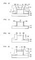
- FIG. 1is a schematic diagram illustrating an exemplary fin field-effect transistor (finFET) device according to an embodiment of the present invention
- FIGS. 2A and 2Bare cross-sectional diagrams illustrating the formation of fins (channels) and a gate dielectric of the finFET device of FIG. 1 according to an embodiment of the present invention
- FIGS. 2C-Fare cross-sectional diagrams illustrating the creation of a dual Vt gate of the finFET device of FIG. 1 according to an embodiment of the present invention
- FIGS. 2G-Iare cross-sectional diagrams illustrating the formation of source/drain regions of the finFET device of FIG. 1 according to an embodiment of the present invention
- FIG. 3is a schematic diagram illustrating an exemplary metal-oxide semiconductor field-effect transistor (MOSFET) device according to an embodiment of the present invention
- FIGS. 4A and 4Bare cross-sectional diagrams illustrating the creation of a base and gate dielectric for the MOSFET device of FIG. 3 according to an embodiment of the present invention
- FIGS. 4C-Lare cross-sectional diagrams illustrating the creation of a dual Vt gate of the MOSFET device of FIG. 3 according to an embodiment of the present invention
- FIGS. 4M-Oare cross-sectional diagrams illustrating the formation of source/drain regions of the MOSFET device of FIG. 3 according to an embodiment of the present invention.
- FIG. 5is a table illustrating performance of two single Vt FET devices and a dual Vt FET device according to an embodiment of the present invention.
- FETField-effect transistor
- Vt'sthreshold voltages
- a number of different FET device designswill be presented each of which is configured with a multiple Vt gate due to the selective placement of one or more band edge metals throughout the gate (see below).
- the first devices presentedare dual Vt finFET devices.
- FIG. 1is a schematic diagram illustrating an exemplary finFET device 100 .
- FinFET device 100includes a source region 106 , a drain region 108 and a plurality of fins 110 interconnecting the source and drain regions.
- Fins 110are patterned in a silicon-on-insulator (SOI) layer wherein the insulator is a buried oxide (BOX) 104 .
- SOIsilicon-on-insulator
- BOXburied oxide
- a gate 112surrounds at least a portion of each of fins 110 .
- Fins 110serve as channels of the device.
- Each finhas two sides (a first side and a second side opposite the first side).
- a portion of the gate adjacent to the first side of each finis configured to have a threshold voltage Vt 1 and a portion of the gate adjacent to the second side of each fin is configured to have a threshold voltage Vt 2 , wherein Vt 2 is different from Vt 1 (i.e., a differential threshold voltage) due to at least one band edge metal being present in the portion of the gate adjacent to the first side of each fin.
- FIGS. 2A-Iare diagrams illustrating an exemplary methodology for fabricating a finFET device, such as finFET device 100 described in conjunction with the description of FIG. 1 , above.
- FIGS. 2A and 2Bhighlight, by way of reference to cross-sectional views through plane A (see FIG. 1 ), the formation of fins (channels) and a gate dielectric.
- FIGS. 2C-Fhighlight, by way of reference to cross-sectional views through plane A (see FIG. 1 ), the creation of a dual Vt gate over the fins.
- FIGS. 2G-Ihighlight, by way of reference to views from vantage point B (see FIG. 1 ), the formation of source/drain regions of the device.
- the starting platform for the deviceis a conventional SOI wafer having a SOI layer over a BOX.
- a substrateis typically present adjacent to a side of the BOX opposite the SOI layer (not shown in the instant diagrams).
- a plurality of fins 202are patterned, i.e., using standard patterning techniques, in the SOI layer over the BOX, i.e., BOX 204 .
- Each fin 202 patterned in this mannerwill have two sides (opposite one another) and a top.
- the sidesare hereinafter referred to as a first side and a second side, with the first side arbitrarily referring to a left side of each fin and the second side arbitrarily referring to a right side of each fin (based on the representations shown in FIG. 2A ). Further, as shown in FIG. 2A , all of the fins have a common orientation wherein the first side of each fin faces one direction (e.g., to the left) and the second side of each fin faces the opposite direction (e.g., to the right).
- dielectric layer 206is formed over exposed portions of BOX 204 and over each fin 202 patterned in the SOI layer.
- Dielectric layer 206can include one or more of silicon dioxide (SiO 2 ) and silicon oxynitride (SiON) and can be deposited using standard thermal oxidation or rapid thermal process (RTP) oxidation to a thickness of from about 0.7 nanometers (nm) to about three nm.
- RTPrapid thermal process
- dielectric layer 206can include a hafnium-based high-k material, such as hafnium oxide (HfO 2 ), hafnium zirconate (HfZrO 4 ), hafnium silicate (HfSiO) and/or nitrided hafnium silicate (HfSiON), and can be deposited using a suitable high-k material deposition process, such as chemical vapor deposition (CVD) or atomic layer deposition (ALD), to a thickness of from about one nm to about five nm.
- CVDchemical vapor deposition
- ALDatomic layer deposition
- Dielectric layer 206will separate each fin 202 from a gate of the device, and thus dielectric layer 206 serves as a gate dielectric.
- the formation of the gatebegins, as shown in FIG. 2C , with the deposition of a first metal layer 208 over the dielectric layer.
- the first metal layercan include titanium nitride (TiN), tantalum nitride (TaN) and/or tantalum carbide (TaC) and can be deposited using ALD to a thickness of from about five nm to about 50 nm.
- the first metal layerdoes not include any band edge metal.
- a concentration of the band edge metal in the first metal layeris less than a concentration of a band edge metal in the second metal layers, see FIG. 2D , described below.
- a series of second metal layers 210are selectively deposited over portions of first metal layer 208 at the top and at one of the sides of each fin. While FIG. 2D depicts selective deposition on the second side of each fin, this is merely exemplary, as the series of second metal layers 210 can, alternatively, be selectively deposited on the first side of each fin.
- This selective depositioncan be achieved using directional deposition techniques and/or differential deposition techniques (e.g., as illustrated by arrows 211 ).
- second metal layers 210can be deposited using thermal evaporation or electron-beam (e-beam) evaporation.
- second metal layers 210include a conventional gate metal, such as TiN, TaN and/or TaC, doped with at least one band edge metal.
- the particular band edge metal(s) used in second metal layers 210can vary depending on whether the finFET device being fabricated is an n-channel finFET (abbreviated herein as “NFET”) or a p-channel finFET (abbreviated herein as “PFET”).
- the band edge metal(s)can include any group IIA (alkaline earth metals)/group IIIB (lanthanides) column element, such as one or more of magnesium (Mg), barium (Ba), strontium (Sr) (group IIA), lanthanum (La), yttrium (Y), dysprosium (Dy), cerium (Ce), praseodymium (Pr), ytterbium (Yb) and lutetium (Lu) (group IIIB).
- group IIAalkaline earth metals
- group IIIBlanthanides
- the band edge metal(s)can include one or more of aluminum (Al), rhodium (Rh), rhenium (Re), platinum (Pt), tungsten (W), nickel (Ni), cobalt (Co), aluminum dioxide (AlO 2 ), titanium dioxide (TiO 2 ), tantalum oxide (Ta 2 O 5 ), nickel oxide (NiO) and cobalt oxide (Co 2 O 3 ).
- second metal layers 210are formed by first depositing the conventional gate metal onto the desired side (i.e., either first side or second side) of each fin over first metal layer 208 using, e.g., thermal evaporation or e-beam evaporation to a thickness of from about five nm to about 50 nm.
- the appropriate band edge metal(s)is then deposited over the conventional gate metal again using, e.g., thermal evaporation or e-beam evaporation to a thickness of from about one angstrom ( ⁇ ) to about 20 ⁇ (the thickness depending on the desired concentration of the band edge metal in the second metal layers).
- the conventional and band edge metalsare then interdiffused throughout second metal layers 210 using an annealing process which can be conducted immediately after the metal depositions, or alternatively, after completion of the gate as a final source/drain activation anneal (see below).
- the parameters used for such annealing processesare well known to those of skill in the art and thus are not described further herein.
- a portion of the gate adjacent to the first side of each finwill have a threshold voltage Vt 1 due to the presence of first metal layer 208 (e.g., a non-band edge metal) in the portion of the gate adjacent to the first side of each fin, and the second side of each fin will have a threshold voltage Vt 2 , wherein Vt 2 is different from Vt 1 due to the presence of second metal layer 210 (e.g., having a band edge metal) in the portion of the gate adjacent to the second side of each fin.
- a width of each fin(labeled w in FIG. 2D ) is generally small enough that any Vt contribution from a portion of the gate adjacent to the top of each fin can be neglected.
- Vt 2⁇ Vt 1 because the band edge metal(s) will typically lower the Vt. Therefore, as highlighted above, if a band edge metal is present in both the first and the second metal layers and if more band edge metal is present in the second metal layers, then the portion of the gate adjacent to the second side of each fin will have a lower Vt than the portion of the gate adjacent to the first side of each fin.
- a finFET device with these propertieswill operate excellently in low supply voltage (V dd ) (Vt 2 >V dd >Vt 1 ), low power mode. When the V dd is increased above Vt 2 , the device will operate in a high performance mode.
- third metal layer 212is deposited over first metal layer 208 and second metal layers 210 .
- Third metal layer 212can include TiN, TaN and/or TaC and can be deposited using CVD or ALD to a thickness of from about five nm to about 50 nm.
- a polysilicon layeri.e., polysilicon layer 214
- polysilicon layer 214can optionally be deposited over third metal layer 212 .
- Polysiliconmakes the gate compatible with subsequent self-aligned silicidation (when the source/drain regions are silicided).
- a contact scheme that is compatible with a metal gatewould eliminate the need for the polysilicon layer.
- some metal gatessuch as TiN/TaN) have lower conductance than silicided polysilicon, so the polysilicon gate that received subsequent silicidation might have lower resistance along the gate.
- Polysilicon layer 214can be deposited using CVD, plasma enhanced chemical vapor deposition (PECVD) or rapid thermal chemical vapor deposition (RTCVD) to a thickness of from about 30 nm to about 150 nm.
- PECVDplasma enhanced chemical vapor deposition
- RTCVDrapid thermal chemical vapor deposition
- any further standard processing of the gatemay then be carried out, if required.
- the finscan be annealed, e.g., to interdiffuse the metals in the metal layers as described above. The gate is now completed.
- FIG. 2Gshows completed gate 216 formed over fins 202 as described above.
- FIGS. 2G-Iillustrate the formation of either a source region or a drain region on one side of the gate, however it is to be understood that the same processes apply to forming the counterpart source region or drain region on the opposite side of the gate.
- offset spacers 218are formed on either side of gate 216 .
- the offset spacersinclude silicon nitride (SiN).
- Extension implants into fins 202 in the source/drain regionsis also performed. As shown in FIG. 2I , epitaxial Si 220 is grown over fins 202 . Offset spacers 218 (see FIG. 2H ) are removed and replaced by final spacers 222 . Source/drain implants are then introduced to the region, followed by a rapid thermal anneal. As a result, source/drain region 224 is formed. Silicide contacts (not shown) to the source/drain regions may also be formed. The specific parameters for source region/drain region and silicide formation techniques are well known to those of skill in the art and thus are not described further herein.
- MOSFETmetal-oxide semiconductor field-effect transistor
- FIG. 3is a schematic diagram illustrating exemplary MOSFET device 300 .
- MOSFET device 300includes a source region 302 , a drain region 304 , a channel 306 interconnecting source region 302 and drain region 304 and a gate 308 surrounding at least a portion of channel 306 .
- gate 308has a dual Vt design, wherein two sides of gate 308 have a first threshold voltage Vt 1 and a top of gate 308 has a second threshold voltage Vt 2 due to the selective placement of one or more band edge metals throughout the gate.
- the use of a dual Vt gate designallows MOSFET device 300 to be run in either a low active power mode or a high performance mode, thus providing savings through an overall reduced power consumption without undesirable performance degradation.
- FIGS. 4A-Oare cross-sectional diagrams illustrating an exemplary methodology for forming a MOSFET device, such as MOSFET device 300 described in conjunction with the description of FIG. 3 , above.
- FIGS. 4A and 4Bhighlight, by way of reference to cross-sectional views through plane a (see FIG. 3 ), the creation of a base for the device and a gate dielectric layer over the base that will separate a portion of the base that will serve as a channel of the device from a gate of the device. See below.
- FIGS. 4C-Lhighlight, by way of reference to cross-sectional views through plane a (see FIG. 3 ), the creation of a dual Vt gate.
- the MOSFET devices described hereinare trigate devices.
- a trigateincludes three active portions, in this case a top surface and two sides.
- the sides of the trigateare both configured to have a same threshold voltage Vt 1 while the top is configured to have a different threshold voltage Vt 2 (this configuration is referred to herein as a “dual Vt” configuration).
- a device with these propertieswill operate excellently in a low power mode when a low supply voltage (V dd ) is provided, i.e., Vt 2 >V dd >Vt 1 .
- V ddlow supply voltage
- Vt 2>V dd >Vt 1 .
- Vt 2When V dd is increased above Vt 2 , the device will operate in a high performance mode.
- Trigate devicesare receiving substantial attention as candidates for 22 nm technologies and beyond. Trigate devices offer better electrostatic control, permitting gate length scaling.
- the current available per planar layoutincreases (i.e., as compared to conventional planar configurations), as the sides are now gated regions.
- the starting platform for the devicecan be a SOI wafer or a bulk silicon wafer.
- a SOI wafer having an SOI layer over a BOXis chosen for use in the instant description.
- the SOI layer of the waferis patterned, e.g., using standard lithography techniques, to form a base 402 for the device over the BOX, i.e., BOX 404 .
- An SOI wafercommonly also includes a substrate adjacent to a side of the BOX opposite the SOI layer, which is not shown in the instant diagrams.
- a source region, a drain region and a gatewill be formed over base 402 with a portion of the base between the source and drain regions and under the gate serving as a channel of the device.
- the gatewill be configured as a trigate having two sides (a first side and a second side opposite the first side) and a top. Accordingly, base 402 has a first side, a second side opposite the first side and a top which will correspond to the first side, second side and top of the gate, respectively, adjacent thereto.
- the starting SOI wafercan be partially or fully depleted.
- SOT thickness T SOIis greater than or equal to 30 nm
- T SOIis less than or equal to 30 nm
- the waferis preferably fully depleted.
- dielectric layer 406is then formed over base 402 and exposed portions of BOX 404 .
- Dielectric layer 406will separate the channel of the device from a gate of the device and thus dielectric layer 406 serves as a gate dielectric.
- Dielectric layer 406can include one or more of SiO 2 and SiON and can be formed using standard thermal or RTP oxidation to a thickness of from about 0.7 nm to about three nm.
- dielectric layer 406can include a hafnium-based high-k material, such as HfO 2 , HfZrO 4 , HfSiO and/or HfSiON and can be formed using CVD or ALD to a thickness of from about one nm to about five nm.
- a high-k dielectricis preferable in situations where metal gates are used and/or when a dielectric with scaling properties advantageous to SiO 2 is required.
- metal layer 408includes a conventional gate metal, such as TiN, TaN and/or TaC, doped with at least one band edge metal.
- the particular band edge metal(s) used in metal layer 408can vary depending on whether the MOSFET device being formed is an n-channel MOSFET (NMOSFET) or a p-channel MOSFET device (PMOSFET).
- the band edge metal(s)can include a group IIA (alkaline earth metals)/group IIIB (lanthanides) column element, such as one or more of Mg, Ba, Sr (group IIA), La, Y, Dy, Ce, Pr, Yb and Lu (group IIIB).
- group IIAalkaline earth metals
- group IIIBlanthanides
- the band edge metal(s)can include one or more of Al, Rh, Re, Pt, W, Ni, Co, AlO 2 , TiO 2 , Ta 2 O 5 , NiO and Co 2 O 3 .
- metal layer 408is formed by first depositing the conventional gate metal over dielectric layer 406 using CVD, ALD, sputtering or thermal evaporation to a thickness of from about five nm to about 50 nm.
- the appropriate band edge metal(s)is then deposited over the conventional gate metal again using CVD, ALD, sputtering or thermal evaporation to a thickness of from about two A to about three A.
- the conventional and band edge metalsare then interdiffused throughout metal layer 408 using an annealing process which can be conducted immediately after the metal depositions, or alternatively, after completion of the gate as part of a final source/drain activation anneal.
- the parameters used for such annealing processesare well known to those of skill in the art and thus are not described further herein.
- an offset spacer precursor layer 410is deposited over metal layer 408 .
- Spacer precursor layer 410can include one or more of polysilicon or amorphous silicon and can be conformally deposited over metal layer 408 using CVD, PECVD or RTCVD to a thickness of from about three nm to about 15 nm.
- Spacer precursor layer 410can be predoped in situ with phosphorus (P) or arsenic (As) for NMOSFET or boron (B) for PMOSFET if an additional band edge metal layer is going to be used (see, for example, FIGS. 4G-I , described below).
- spacer precursor layer 410may also include a non-conductive dielectric, such as SiN, since the offset spacers formed therefrom will be subsequently removed during processing, see below.
- offset spacers 412 and 414are then formed from spacer precursor layer 410 on each side of base 402 adjacent to metal layer 408 .
- RIEreactive ion etching
- the portion of metal layer 408 exposed by the RIEis selectively removed from the top of base 402 (i.e., from over a portion of the dielectric layer on top of the base), for example, using wet etching.
- This processessentially forms two separate layers from metal layer 408 , one on each side (i.e., on the first side and second side) of base 402 (referred to hereinafter as a first metal layer 408 a and a second metal layer 408 b ).
- first metal layerwill be used to refer to the portion of metal layer 408 that remains to a left (first) side of base 402 adjacent to the dielectric layer and the term “second metal layer” will be used to refer to the portion of metal layer 408 that remains to a right (second) side of base 402 adjacent to the dielectric layer. This name assignment is however arbitrary.
- first metal layer 408 a and second metal layer 408 boriginate from the same metal layer (metal layer 408 ), first metal layer 408 a and second metal layer 408 b have a same (or approximately the same) composition and physical properties, such as thickness.
- the steps takencan vary depending on whether or not another metal layer, i.e., a third metal layer including a different band edge metal(s) is employed.
- FIGS. 4G-Idepict the use of a third metal layer in the trigate
- FIGS. 4J-Ldepict a trigate without a third metal layer.
- the channel dopinghas to be greatly reduced as compared to a band edge device, i.e., typically reduced by from about 30 percent (%) to about 60%. The reduced channel doping degrades the short channel response. If the channel doping is not reduced, the Vt will be typically too high.
- a MOSFET device with a thinner basesuch as fully depleted SOI (i.e., T SOI ⁇ 30 nm) doping no longer sets the Vt.
- a quarter gap and/or mid-gap metalwould provide acceptable Vt in many cases. Therefore, by way of example only, for the thicker, partially depleted SOI (or bulk silicon)-based devices, the top and sides of the gate would probably need band edge metals applied ( FIGS. 4G-I ), unless a very much larger Vt (e.g., from about 800 millivolts (mV) to about one volt (V)) for the top of the gate is needed.
- band edge metals at the sides and top of the gatecould still be used, but the likelihood increases that the band edge metal at the top of the gate could be omitted, as this Vt would not be as high in a fully depleted device.
- the band edge metal(s)would be used only at the sides of the gate ( FIGS. 4J-L ). Incentives to omit the additional band edge metal would be lower process costs and process simplification.
- third metal layer 416is deposited over a portion of dielectric layer 406 on top of base 402 and over offset spacers 412 / 414 .
- third metal layer 416also includes a conventional gate metal, such as TiN, TaN and/or TaC, doped with at least one band edge metal.
- the band edge metal in third metal layer 416is different from the band edge metal in first and second metal layers 408 a and 408 b (in order to achieve a dual Vt trigate).
- Third metal layer 416can include one or more of the following band edge metals, Mg, Ba, Sr (group IIA), La, Y Dy, Ce, Pr, Yb and Lu (group IIIB) for NMOSFET, and Al, Rh, Re, Pt, W, Ni, Co, AlO 2 , TiO 2 , Ta 2 O 5 , NiO and Co 2 O 3 for PMOSFET.
- third metal layer 416is formed by first depositing the conventional gate metal over the top of the gate stack, offset spacers 412 / 414 and dielectric layer 406 using CVD, ALD, sputtering or thermal evaporation to a thickness of from about five nm to about 50 nm.
- the appropriate band edge metal(s)is then deposited over the conventional gate metal again using CVD, ALD, sputtering or thermal evaporation to a thickness of from about two A to about three A.
- the conventional and band edge metalsare then interdiffused throughout third metal layer 416 using an annealing process which can be conducted immediately after the metal depositions, or alternatively, after completion of the gate as part of a final source/drain activation anneal.
- top electrode layer 418is deposited over third metal layer 416 .
- Top electrode layer 418can include one or more of TiN, TaC and TaN, and can be deposited over third metal layer 416 using ALD to a thickness of from about five nm to about 50 nm.
- polysilicon layer 420may be deposited over top electrode layer 418 .
- This stepis optional.
- a polysilicon layermay be used to make the gate compatible with subsequent self-aligned silicidation (i.e., when the source/drain regions of the device are silicided).
- a contact scheme that is compatible with a metal gatewould eliminate the need for the polysilicon layer.
- some metal gatessuch as TiN/TaN have lower conductance than silicided polysilicon, so the polysilicon gate that received subsequent silicidation might have lower resistance along the gate.
- Polysilicon layer 420can be deposited over top electrode layer 418 using CVD, PECVD or RTCVD to a thickness of from about 30 nm to about 150 nm. Polysilicon layer 420 can be either pre-doped or doped later during source/drain formation.
- the gatewill have a dual Vt configuration with the sides (i.e., S 1 and S 2 ) of the gate both having a first threshold voltage, i.e., threshold voltage Vt 1 , and the top (i.e., T) of the gate having a second threshold voltage, i.e., threshold voltage Vt 2 , wherein Vt 2 >Vt 1 .
- Vt 1can be varied relative to Vt 2 and vice versa, e.g., by varying one or more of the content and thickness of first metal layer/second metal layer and/or the third metal layer.
- FIGS. 4J-Ldepict a trigate without a second band edge metal.
- offset spacers 412 and 414which were left undoped (see above), are removed. Offset spacers 412 and 414 can be removed using wet etching or a silicon-specific RIE.
- top electrode layer 422is deposited over first and second metal layers 408 a and 408 b /dielectric layer 406 (i.e., over a portion of the dielectric layer on top of the base).
- Top electrode layer 422can include doped polysilicon or a metal, such as TiN, TaC or TaN.
- top electrode layer 422includes TiN and is deposited using ALD to a thickness of from about five nm to about 50 nm.
- a polysilicon layer 424may be deposited over top electrode layer 422 . This step is optional. As highlighted above, a polysilicon layer may be used to make the gate compatible with subsequent self-aligned silicidation (i.e., when the source/drain regions of the device are silicided). Like polysilicon layer 420 , described above, polysilicon layer 424 can be deposited using CVD, PECVD or RTCVD to a thickness of from about 30 nm to about 150 nm. Polysilicon layer 424 can be either pre-doped or doped later during source/drain formation.
- the gatewill have a dual Vt configuration with the sides (i.e., S 1 and S 2 ) of the gate both having a first threshold voltage, i.e., threshold voltage Vt 1 , and the top (i.e., T) of the gate having a second threshold voltage, i.e., threshold voltage Vt 2 , wherein Vt 2 >Vt 1 .
- Vt 1can be varied relative to Vt 2 and vice versa, e.g., by varying one or more of the content and thickness of first and second band edge metal layers 408 a and 408 b.
- gate lithography and subsequent etch processesare used to form the gate stack. These lithography and etching steps are known to those of skill in the art and thus are not described further herein.
- the gateis self-aligned, in that the top and sides of the gate are preferably formed with only one lithography and subsequent etch step. Therefore, the top and sides are aligned to each other.
- any further standard processing of the gatemay then be carried out, if required.
- the gatecan be annealed, e.g., to interdiffuse the metals in the metal layers as described above. The gate is now completed.
- FIG. 4Mshows a completed trigate formed as described above.
- the particular trigate shown in this exampledoes not have a second band edge metal, however, either trigate configuration (with or without a second band edge metal) applies to this description.
- FIGS. 4N-Oillustrate the formation of either a source region or a drain region on one side of the trigate, however it is to be understood that the same processes apply to forming the counterpart source region or drain region on the opposite side of the trigate.
- offset spacers 428are formed on either side of the trigate.
- the offset spacersinclude SiN. Dopants are introduced into BOX 404 in the source/drain regions (and into the polysilicon layer if not pre-doped (see above)). As shown in FIG. 4O , epitaxial silicon 430 is grown in the source/drain regions and offset spacers 428 (see FIG. 4N ) are removed and replaced by final spacers 432 . Source/drain implants are introduced to the region, followed by a rapid thermal anneal. As a result, the source/drain regions are formed. Silicide contacts (not shown) to the source/drain regions may also be formed. The specific parameters for source region/drain region and silicide formation techniques are well known to those of skill in the art and thus are not described further herein. As highlighted above, the channel formed from the base extends between the source and drain regions.
- a trigate device having a thick basee.g., a T SOI or T silicon of greater than or equal to about 25 nm
- a trigate device having a thick basee.g., a T SOI or T silicon of greater than or equal to about 25 nm
- the epitaxially grown source/drain growthmay not be needed and this region may instead be directly implanted (see above) and silicided to form the source/drain region.
- the trigatehas a side:top:side aspect ratio of about 1:1:1.
- the top of the gatewill contribute about 1 ⁇ 3 of the total MOSFET contribution.
- the top of the gatehas a significant importance, relative to the sides of the gate.
- Other configurationsare presented in the Examples below, however wherein the aspect ratio is scaled.
- a dual Vt finFET device(e.g., fabricated according to the methodology outlined in FIGS. 2A-I , above) and a conventional single Vt finFET device were compared at two V dd levels, i.e., a V dd1 of one V and a V dd2 of 0.5V (wherein a ⁇ Vt, i.e., a difference between Vt 1 and Vt 2 , of about 400 mV was assumed).
- V dd1 V or 0.5 V.
- Vt 1300 mV
- Vt 2600 mV.
- constant device widthswhich means no re-design of existing device designs. Namely, it is assumed that the circuit and device design itself remains constant.
- the integration of trigatescan easily be accomplished without altering masks, the same masks are simply implemented using different processes to get a trigate.
- a migration re-mapwould require circuit designers to modify circuits and the resulting physical layout (masks). Re-maps are typically very costly and time consuming, whereas an integration solution (such as with the present techniques) that does not alter the physical masks has a much quicker turnaround time and less associated costs.
- Drive current Iis normalized to be one V drive of the 300 mV single Vt case (see above and FIG. 5 (described below)). 3) A 10% drive loss per 100 mV overdrive is assumed. Overdrive is the amount of gate voltage greater than Vt.
- Case 3dual Vt
Landscapes
- Thin Film Transistor (AREA)
- Insulated Gate Type Field-Effect Transistor (AREA)
- Metal-Oxide And Bipolar Metal-Oxide Semiconductor Integrated Circuits (AREA)
- Electrodes Of Semiconductors (AREA)
Abstract
Description
Claims (16)
Priority Applications (1)
| Application Number | Priority Date | Filing Date | Title |
|---|---|---|---|
| US13/346,165US8878298B2 (en) | 2009-04-21 | 2012-01-09 | Multiple Vt field-effect transistor devices |
Applications Claiming Priority (2)
| Application Number | Priority Date | Filing Date | Title |
|---|---|---|---|
| US12/427,247US8110467B2 (en) | 2009-04-21 | 2009-04-21 | Multiple Vt field-effect transistor devices |
| US13/346,165US8878298B2 (en) | 2009-04-21 | 2012-01-09 | Multiple Vt field-effect transistor devices |
Related Parent Applications (1)
| Application Number | Title | Priority Date | Filing Date |
|---|---|---|---|
| US12/427,247DivisionUS8110467B2 (en) | 2009-04-21 | 2009-04-21 | Multiple Vt field-effect transistor devices |
Publications (2)
| Publication Number | Publication Date |
|---|---|
| US20120175712A1 US20120175712A1 (en) | 2012-07-12 |
| US8878298B2true US8878298B2 (en) | 2014-11-04 |
Family
ID=42980363
Family Applications (2)
| Application Number | Title | Priority Date | Filing Date |
|---|---|---|---|
| US12/427,247Active2030-01-28US8110467B2 (en) | 2009-04-21 | 2009-04-21 | Multiple Vt field-effect transistor devices |
| US13/346,165ActiveUS8878298B2 (en) | 2009-04-21 | 2012-01-09 | Multiple Vt field-effect transistor devices |
Family Applications Before (1)
| Application Number | Title | Priority Date | Filing Date |
|---|---|---|---|
| US12/427,247Active2030-01-28US8110467B2 (en) | 2009-04-21 | 2009-04-21 | Multiple Vt field-effect transistor devices |
Country Status (6)
| Country | Link |
|---|---|
| US (2) | US8110467B2 (en) |
| EP (1) | EP2396812B1 (en) |
| JP (1) | JP5552155B2 (en) |
| CN (1) | CN102405516B (en) |
| TW (1) | TWI476918B (en) |
| WO (1) | WO2010123750A1 (en) |
Cited By (6)
| Publication number | Priority date | Publication date | Assignee | Title |
|---|---|---|---|---|
| US9287408B2 (en) | 2011-03-25 | 2016-03-15 | Semiconductor Energy Laboratory Co., Ltd. | Field-effect transistor, and memory and semiconductor circuit including the same |
| US10002791B1 (en) | 2017-04-06 | 2018-06-19 | International Business Machines Corporation | Multi-layer work function metal gates with similar gate thickness to achieve multi-Vt for vFETS |
| US20180301539A1 (en)* | 2011-08-23 | 2018-10-18 | Micron Technology, Inc. | Semiconductor devices and structures and methods of formation |
| US10290634B2 (en) | 2016-01-20 | 2019-05-14 | Globalfoundries Inc. | Multiple threshold voltages using fin pitch and profile |
| US10446400B2 (en) | 2017-10-20 | 2019-10-15 | Samsung Electronics Co., Ltd. | Method of forming multi-threshold voltage devices and devices so formed |
| US10985075B2 (en) | 2018-10-11 | 2021-04-20 | International Business Machines Corporation | Gate formation scheme for n-type and p-type transistors having separately tuned threshold voltages |
Families Citing this family (31)
| Publication number | Priority date | Publication date | Assignee | Title |
|---|---|---|---|---|
| US8422273B2 (en) | 2009-05-21 | 2013-04-16 | International Business Machines Corporation | Nanowire mesh FET with multiple threshold voltages |
| US8426923B2 (en)* | 2009-12-02 | 2013-04-23 | Taiwan Semiconductor Manufacturing Company, Ltd. | Multiple-gate semiconductor device and method |
| US8753942B2 (en) | 2010-12-01 | 2014-06-17 | Intel Corporation | Silicon and silicon germanium nanowire structures |
| KR20120125017A (en)* | 2011-05-06 | 2012-11-14 | 삼성전자주식회사 | Semiconductor device and method for fabricating the device |
| CN102956496B (en)* | 2011-08-30 | 2015-06-03 | 中芯国际集成电路制造(上海)有限公司 | Fin type field effect transistor and manufacturing method thereof |
| US8637931B2 (en)* | 2011-12-27 | 2014-01-28 | International Business Machines Corporation | finFET with merged fins and vertical silicide |
| US8643120B2 (en)* | 2012-01-06 | 2014-02-04 | International Business Machines Corporation | FinFET with fully silicided gate |
| US20130241007A1 (en) | 2012-03-15 | 2013-09-19 | International Business Machines Corporation | Use of band edge gate metals as source drain contacts |
| KR101909205B1 (en)* | 2012-04-20 | 2018-10-17 | 삼성전자 주식회사 | Semiconductor device including fin-type field effect transistor |
| US8802535B2 (en) | 2012-05-02 | 2014-08-12 | International Business Machines Corporation | Doped core trigate FET structure and method |
| KR101909091B1 (en)* | 2012-05-11 | 2018-10-17 | 삼성전자 주식회사 | Semiconductor device and fabricating method thereof |
| US8962434B2 (en) | 2012-07-10 | 2015-02-24 | International Business Machines Corporation | Field effect transistors with varying threshold voltages |
| US9093556B2 (en) | 2012-08-21 | 2015-07-28 | Stmicroelectronics, Inc. | Multi-fin FINFET device including epitaxial growth barrier on outside surfaces of outermost fins and related methods |
| US8999831B2 (en) | 2012-11-19 | 2015-04-07 | International Business Machines Corporation | Method to improve reliability of replacement gate device |
| US9633835B2 (en)* | 2013-09-06 | 2017-04-25 | Intel Corporation | Transistor fabrication technique including sacrificial protective layer for source/drain at contact location |
| KR102176513B1 (en) | 2013-09-25 | 2020-11-09 | 인텔 코포레이션 | Isolation well doping with solid-state diffusion sources for finfet architectures |
| US9373720B2 (en)* | 2013-10-14 | 2016-06-21 | Globalfoundries Inc. | Three-dimensional transistor with improved channel mobility |
| US9112030B2 (en)* | 2013-11-04 | 2015-08-18 | United Microelectronics Corp. | Epitaxial structure and process thereof for non-planar transistor |
| US9219155B2 (en)* | 2013-12-16 | 2015-12-22 | Intel Corporation | Multi-threshold voltage devices and associated techniques and configurations |
| US9484205B2 (en) | 2014-04-07 | 2016-11-01 | International Business Machines Corporation | Semiconductor device having self-aligned gate contacts |
| US9590105B2 (en)* | 2014-04-07 | 2017-03-07 | National Chiao-Tung University | Semiconductor device with metal alloy over fin, conductive layer over channel region of fin, and semiconductive layer over conductive layer and formation thereof |
| JP6629312B2 (en)* | 2014-07-03 | 2020-01-15 | アプライド マテリアルズ インコーポレイテッドApplied Materials,Incorporated | Method and apparatus for selective deposition |
| US9484270B2 (en) | 2014-09-16 | 2016-11-01 | International Business Machines Corporation | Fully-depleted silicon-on-insulator transistors |
| US9553092B2 (en) | 2015-06-12 | 2017-01-24 | Globalfoundries Inc. | Alternative threshold voltage scheme via direct metal gate patterning for high performance CMOS FinFETs |
| DE112015006974T5 (en) | 2015-09-25 | 2019-01-24 | Intel Corporation | A method of doping fin structures of non-planar transistor devices |
| US9543297B1 (en)* | 2015-09-29 | 2017-01-10 | Globalfoundries Inc. | Fin-FET replacement metal gate structure and method of manufacturing the same |
| US9806078B1 (en)* | 2016-11-02 | 2017-10-31 | Globalfoundries Inc. | FinFET spacer formation on gate sidewalls, between the channel and source/drain regions |
| US10522643B2 (en) | 2017-04-26 | 2019-12-31 | Taiwan Semiconductor Manufacturing Co., Ltd. | Device and method for tuning threshold voltage by implementing different work function metals in different segments of a gate |
| US10886393B2 (en)* | 2017-10-17 | 2021-01-05 | Mitsubishi Electric Research Laboratories, Inc. | High electron mobility transistor with tunable threshold voltage |
| US10461078B2 (en)* | 2018-02-26 | 2019-10-29 | Taiwan Semiconductor Manufacturing Co., Ltd. | Creating devices with multiple threshold voltage by cut-metal-gate process |
| KR102481284B1 (en)* | 2018-04-10 | 2022-12-27 | 삼성전자주식회사 | A method of manufacturing semiconductor device |
Citations (47)
| Publication number | Priority date | Publication date | Assignee | Title |
|---|---|---|---|---|
| US5352624A (en) | 1992-01-23 | 1994-10-04 | Sony Corporation | SOI type semiconductor device and manufacturing method therefor |
| US6146970A (en) | 1998-05-26 | 2000-11-14 | Motorola Inc. | Capped shallow trench isolation and method of formation |
| US6448590B1 (en) | 2000-10-24 | 2002-09-10 | International Business Machines Corporation | Multiple threshold voltage FET using multiple work-function gate materials |
| US6492212B1 (en) | 2001-10-05 | 2002-12-10 | International Business Machines Corporation | Variable threshold voltage double gated transistors and method of fabrication |
| JP2003124463A (en) | 1994-09-14 | 2003-04-25 | Toshiba Corp | Semiconductor device |
| US20030151077A1 (en) | 2002-02-13 | 2003-08-14 | Leo Mathew | Method of forming a vertical double gate semiconductor device and structure thereof |
| US6720619B1 (en) | 2002-12-13 | 2004-04-13 | Taiwan Semiconductor Manufacturing Company, Ltd. | Semiconductor-on-insulator chip incorporating partially-depleted, fully-depleted, and multiple-gate devices |
| US20040150029A1 (en) | 2003-02-04 | 2004-08-05 | Lee Jong-Ho | Double-gate FinFET device and fabricating method thereof |
| US6853020B1 (en) | 2002-11-08 | 2005-02-08 | Advanced Micro Devices, Inc. | Double-gate semiconductor device |
| US6855989B1 (en) | 2003-10-01 | 2005-02-15 | Advanced Micro Devices, Inc. | Damascene finfet gate with selective metal interdiffusion |
| US20050051843A1 (en) | 2003-09-08 | 2005-03-10 | Satoshi Inaba | Semiconductor device and manufacturing method thereof |
| EP1519420A2 (en) | 2003-09-25 | 2005-03-30 | Interuniversitaire Microelectronica Centrum vzw ( IMEC) | Multiple gate semiconductor device and method for forming same |
| US20050093067A1 (en) | 2003-04-30 | 2005-05-05 | Yee-Chia Yeo | Semiconductor-on-insulator chip incorporating strained-channel partially-depleted, fully-depleted, and multiple-gate transistors |
| US20050104096A1 (en)* | 2003-11-17 | 2005-05-19 | Deok-Hyung Lee | FinFETs having first and second gates of different resistivities, and methods of fabricating the same |
| WO2005078804A1 (en) | 2004-02-17 | 2005-08-25 | Samsung Electronics Co., Ltd. | Semiconductor device having multi-gate structure and method of manufacturing the same |
| US20060057787A1 (en) | 2002-11-25 | 2006-03-16 | Doris Bruce B | Strained finfet cmos device structures |
| US20060081895A1 (en) | 2004-10-19 | 2006-04-20 | Deok-Huyng Lee | Semiconductor device having fin transistor and planar transistor and associated methods of manufacture |
| US20060244079A1 (en)* | 2005-04-29 | 2006-11-02 | Wang Xiaoquan | MOS transistor including multi-work function metal nitride gate electrode, COMS integrated circuit device including same, and related methods of manufacture |
| US20060270156A1 (en) | 2004-10-08 | 2006-11-30 | Seong-Gyun Kim | Non-volatile memory devices and methods of forming the same |
| US20060289948A1 (en) | 2005-06-22 | 2006-12-28 | International Business Machines Corporation | Method to control flatband/threshold voltage in high-k metal gated stacks and structures thereof |
| US20070013413A1 (en) | 2005-07-14 | 2007-01-18 | International Business Machines Corporation | High-density logic techniques with reduced-stack multi-gate field effect transistors |
| US20070029623A1 (en) | 2003-12-05 | 2007-02-08 | National Inst Of Adv Industrial Science And Tech | Dual-gate field effect transistor |
| US20070040221A1 (en)* | 2005-08-19 | 2007-02-22 | Harald Gossner | Electrostatic discharge protection element |
| US20070048984A1 (en)* | 2005-08-31 | 2007-03-01 | Steven Walther | Metal work function adjustment by ion implantation |
| US20070075351A1 (en) | 2005-09-30 | 2007-04-05 | Thomas Schulz | Semiconductor devices and methods of manufacture thereof |
| US20070111448A1 (en) | 2005-11-15 | 2007-05-17 | Hong-Jyh Li | Semiconductor devices and methods of manufacture thereof |
| US20070148843A1 (en) | 2005-12-16 | 2007-06-28 | Tomohiro Saito | Semiconductor device and method of manufacturing the same |
| US20070164785A1 (en) | 2004-06-04 | 2007-07-19 | The Regents Of The University Of California | Low-power fpga circuits and methods |
| WO2007085996A2 (en) | 2006-01-30 | 2007-08-02 | Nxp B.V. | Mos device and method of fabricating a mos device |
| US20070184592A1 (en) | 2006-02-01 | 2007-08-09 | Kazuaki Nakajima | Method for manufacturing semiconductor device |
| US7288805B2 (en) | 2005-02-24 | 2007-10-30 | International Business Machines Corporation | Double gate isolation |
| US20070257325A1 (en) | 2006-05-03 | 2007-11-08 | Willy Rachmady | Tri-gate device with conformal PVD workfunction metal on its three-dimensional body and fabrication method thereof |
| US7332386B2 (en) | 2004-03-23 | 2008-02-19 | Samsung Electronics Co., Ltd. | Methods of fabricating fin field transistors |
| US20080050898A1 (en) | 2006-08-23 | 2008-02-28 | Hongfa Luan | Semiconductor devices and methods of manufacture thereof |
| WO2008026859A1 (en) | 2006-09-01 | 2008-03-06 | Kyungpook National University Industry-Academic Cooperation Foundation | Fin field effect transistor haiving low leakage current and method of manufacturing the finfet |
| US20080073723A1 (en)* | 2006-09-22 | 2008-03-27 | Willy Rachmady | Selective anisotropic wet etching of workfunction metal for semiconductor devices |
| US20080111185A1 (en) | 2006-11-13 | 2008-05-15 | International Business Machines Corporation | Asymmetric multi-gated transistor and method for forming |
| US20080116515A1 (en)* | 2006-11-17 | 2008-05-22 | Infineon Technologies Agam Campeon | Mugfet with increased thermal mass |
| WO2008072164A1 (en) | 2006-12-15 | 2008-06-19 | Nxp B.V. | Transistor device and method of manufacturing such a transistor device |
| US20080169512A1 (en) | 2004-08-10 | 2008-07-17 | Doyle Brian S | Non-planar pMOS structure with a strained channel region and an integrated strained CMOS flow |
| US20080175039A1 (en)* | 2006-12-28 | 2008-07-24 | Commissariat A L'energie Atomique | Memory cell provided with dual-gate transistors, with independent asymmetric gates |
| US20090020824A1 (en) | 2007-07-20 | 2009-01-22 | Renesas Technology Corp. | Semiconductor device and method for producing the same |
| US7534669B2 (en) | 2004-01-28 | 2009-05-19 | International Business Machines Corporation | Method and structure to create multiple device widths in FinFET technology in both bulk and SOI |
| US20090134469A1 (en)* | 2007-11-28 | 2009-05-28 | Interuniversitair Microelektronica Centrum (Imec) Vzw | Method of manufacturing a semiconductor device with dual fully silicided gate |
| US7781274B2 (en) | 2008-03-27 | 2010-08-24 | Kabushiki Kaisha Toshiba | Multi-gate field effect transistor and method for manufacturing the same |
| US7859081B2 (en) | 2007-03-29 | 2010-12-28 | Intel Corporation | Capacitor, method of increasing a capacitance area of same, and system containing same |
| US7932564B2 (en) | 2007-06-27 | 2011-04-26 | Kabushiki Kaisha Toshiba | Semiconductor device and method of fabricating the same |
Family Cites Families (2)
| Publication number | Priority date | Publication date | Assignee | Title |
|---|---|---|---|---|
| US7300837B2 (en)* | 2004-04-30 | 2007-11-27 | Taiwan Semiconductor Manufacturing Co., Ltd | FinFET transistor device on SOI and method of fabrication |
| US8124483B2 (en)* | 2007-06-07 | 2012-02-28 | Infineon Technologies Ag | Semiconductor devices and methods of manufacture thereof |
- 2009
- 2009-04-21USUS12/427,247patent/US8110467B2/enactiveActive
- 2010
- 2010-04-14TWTW099111648Apatent/TWI476918B/enactive
- 2010-04-15JPJP2012507269Apatent/JP5552155B2/enactiveActive
- 2010-04-15CNCN201080017383.3Apatent/CN102405516B/enactiveActive
- 2010-04-15WOPCT/US2010/031224patent/WO2010123750A1/enactiveApplication Filing
- 2010-04-15EPEP10767544.9Apatent/EP2396812B1/enactiveActive
- 2012
- 2012-01-09USUS13/346,165patent/US8878298B2/enactiveActive
Patent Citations (61)
| Publication number | Priority date | Publication date | Assignee | Title |
|---|---|---|---|---|
| US5352624A (en) | 1992-01-23 | 1994-10-04 | Sony Corporation | SOI type semiconductor device and manufacturing method therefor |
| JP2003124463A (en) | 1994-09-14 | 2003-04-25 | Toshiba Corp | Semiconductor device |
| US6146970A (en) | 1998-05-26 | 2000-11-14 | Motorola Inc. | Capped shallow trench isolation and method of formation |
| US6448590B1 (en) | 2000-10-24 | 2002-09-10 | International Business Machines Corporation | Multiple threshold voltage FET using multiple work-function gate materials |
| US6797553B2 (en) | 2000-10-24 | 2004-09-28 | International Business Machines Corporation | Method for making multiple threshold voltage FET using multiple work-function gate materials |
| US6492212B1 (en) | 2001-10-05 | 2002-12-10 | International Business Machines Corporation | Variable threshold voltage double gated transistors and method of fabrication |
| US20030067017A1 (en) | 2001-10-05 | 2003-04-10 | Meikei Ieong | Variable threshold voltage double gated transistors and method of fabrication |
| JP2003163356A (en) | 2001-10-05 | 2003-06-06 | Internatl Business Mach Corp <Ibm> | Double gate transistor and method of manufacturing the same |
| US20030151077A1 (en) | 2002-02-13 | 2003-08-14 | Leo Mathew | Method of forming a vertical double gate semiconductor device and structure thereof |
| US6853020B1 (en) | 2002-11-08 | 2005-02-08 | Advanced Micro Devices, Inc. | Double-gate semiconductor device |
| US20060057787A1 (en) | 2002-11-25 | 2006-03-16 | Doris Bruce B | Strained finfet cmos device structures |
| US6720619B1 (en) | 2002-12-13 | 2004-04-13 | Taiwan Semiconductor Manufacturing Company, Ltd. | Semiconductor-on-insulator chip incorporating partially-depleted, fully-depleted, and multiple-gate devices |
| US20040150029A1 (en) | 2003-02-04 | 2004-08-05 | Lee Jong-Ho | Double-gate FinFET device and fabricating method thereof |
| US20050093067A1 (en) | 2003-04-30 | 2005-05-05 | Yee-Chia Yeo | Semiconductor-on-insulator chip incorporating strained-channel partially-depleted, fully-depleted, and multiple-gate transistors |
| US20050051843A1 (en) | 2003-09-08 | 2005-03-10 | Satoshi Inaba | Semiconductor device and manufacturing method thereof |
| EP1519420A2 (en) | 2003-09-25 | 2005-03-30 | Interuniversitaire Microelectronica Centrum vzw ( IMEC) | Multiple gate semiconductor device and method for forming same |
| US6855989B1 (en) | 2003-10-01 | 2005-02-15 | Advanced Micro Devices, Inc. | Damascene finfet gate with selective metal interdiffusion |
| US20050104096A1 (en)* | 2003-11-17 | 2005-05-19 | Deok-Hyung Lee | FinFETs having first and second gates of different resistivities, and methods of fabricating the same |
| US20070029623A1 (en) | 2003-12-05 | 2007-02-08 | National Inst Of Adv Industrial Science And Tech | Dual-gate field effect transistor |
| US7534669B2 (en) | 2004-01-28 | 2009-05-19 | International Business Machines Corporation | Method and structure to create multiple device widths in FinFET technology in both bulk and SOI |
| WO2005078804A1 (en) | 2004-02-17 | 2005-08-25 | Samsung Electronics Co., Ltd. | Semiconductor device having multi-gate structure and method of manufacturing the same |
| US20070272925A1 (en) | 2004-02-17 | 2007-11-29 | Choi Jung-A | Semiconductor Device Having Multi-Gate Structure and Method of Manufacturing the Same |
| US7838915B2 (en) | 2004-02-17 | 2010-11-23 | Samsung Electronics Co.. Ltd. | Semiconductor device having multi-gate structure and method of manufacturing the same |
| US20110033989A1 (en) | 2004-02-17 | 2011-02-10 | Choi Jung-A | Semiconductor device having multi-gate structure and method of manufacturing the same |
| US7332386B2 (en) | 2004-03-23 | 2008-02-19 | Samsung Electronics Co., Ltd. | Methods of fabricating fin field transistors |
| US20070164785A1 (en) | 2004-06-04 | 2007-07-19 | The Regents Of The University Of California | Low-power fpga circuits and methods |
| US20080169512A1 (en) | 2004-08-10 | 2008-07-17 | Doyle Brian S | Non-planar pMOS structure with a strained channel region and an integrated strained CMOS flow |
| US20060270156A1 (en) | 2004-10-08 | 2006-11-30 | Seong-Gyun Kim | Non-volatile memory devices and methods of forming the same |
| US20060081895A1 (en) | 2004-10-19 | 2006-04-20 | Deok-Huyng Lee | Semiconductor device having fin transistor and planar transistor and associated methods of manufacture |
| US7501674B2 (en) | 2004-10-19 | 2009-03-10 | Samsung Electronics Co., Ltd. | Semiconductor device having fin transistor and planar transistor and associated methods of manufacture |
| US7288805B2 (en) | 2005-02-24 | 2007-10-30 | International Business Machines Corporation | Double gate isolation |
| US20070269950A1 (en) | 2005-02-24 | 2007-11-22 | Anderson Brent A | Double gate isolation |
| US20060244079A1 (en)* | 2005-04-29 | 2006-11-02 | Wang Xiaoquan | MOS transistor including multi-work function metal nitride gate electrode, COMS integrated circuit device including same, and related methods of manufacture |
| US20060289948A1 (en) | 2005-06-22 | 2006-12-28 | International Business Machines Corporation | Method to control flatband/threshold voltage in high-k metal gated stacks and structures thereof |
| US20070013413A1 (en) | 2005-07-14 | 2007-01-18 | International Business Machines Corporation | High-density logic techniques with reduced-stack multi-gate field effect transistors |
| US20070040221A1 (en)* | 2005-08-19 | 2007-02-22 | Harald Gossner | Electrostatic discharge protection element |
| US20070048984A1 (en)* | 2005-08-31 | 2007-03-01 | Steven Walther | Metal work function adjustment by ion implantation |
| US20070075351A1 (en) | 2005-09-30 | 2007-04-05 | Thomas Schulz | Semiconductor devices and methods of manufacture thereof |
| US20070111448A1 (en) | 2005-11-15 | 2007-05-17 | Hong-Jyh Li | Semiconductor devices and methods of manufacture thereof |
| US20070148843A1 (en) | 2005-12-16 | 2007-06-28 | Tomohiro Saito | Semiconductor device and method of manufacturing the same |
| WO2007085996A2 (en) | 2006-01-30 | 2007-08-02 | Nxp B.V. | Mos device and method of fabricating a mos device |
| US20070184592A1 (en) | 2006-02-01 | 2007-08-09 | Kazuaki Nakajima | Method for manufacturing semiconductor device |
| JP2007207994A (en) | 2006-02-01 | 2007-08-16 | Toshiba Corp | Manufacturing method of semiconductor device |
| US20070257325A1 (en) | 2006-05-03 | 2007-11-08 | Willy Rachmady | Tri-gate device with conformal PVD workfunction metal on its three-dimensional body and fabrication method thereof |
| US20080157207A1 (en) | 2006-05-03 | 2008-07-03 | Intel Corporation | Tri-gate device with conformal pvd workfunction metal on its three-dimensional body and fabrication method thereof |
| US20080050898A1 (en) | 2006-08-23 | 2008-02-28 | Hongfa Luan | Semiconductor devices and methods of manufacture thereof |
| WO2008026859A1 (en) | 2006-09-01 | 2008-03-06 | Kyungpook National University Industry-Academic Cooperation Foundation | Fin field effect transistor haiving low leakage current and method of manufacturing the finfet |
| US20080073723A1 (en)* | 2006-09-22 | 2008-03-27 | Willy Rachmady | Selective anisotropic wet etching of workfunction metal for semiconductor devices |
| JP2008124457A (en) | 2006-11-13 | 2008-05-29 | Internatl Business Mach Corp <Ibm> | Asymmetric multi-gate transistor and formation method |
| US8679906B2 (en) | 2006-11-13 | 2014-03-25 | International Business Machines Corporation | Asymmetric multi-gated transistor and method for forming |
| US20100044794A1 (en) | 2006-11-13 | 2010-02-25 | International Business Machines Corporation | Asymmetric multi-gated transistor and method for forming |
| US20080111185A1 (en) | 2006-11-13 | 2008-05-15 | International Business Machines Corporation | Asymmetric multi-gated transistor and method for forming |
| US20080116515A1 (en)* | 2006-11-17 | 2008-05-22 | Infineon Technologies Agam Campeon | Mugfet with increased thermal mass |
| WO2008072164A1 (en) | 2006-12-15 | 2008-06-19 | Nxp B.V. | Transistor device and method of manufacturing such a transistor device |
| US20080175039A1 (en)* | 2006-12-28 | 2008-07-24 | Commissariat A L'energie Atomique | Memory cell provided with dual-gate transistors, with independent asymmetric gates |
| US7859081B2 (en) | 2007-03-29 | 2010-12-28 | Intel Corporation | Capacitor, method of increasing a capacitance area of same, and system containing same |
| US7932564B2 (en) | 2007-06-27 | 2011-04-26 | Kabushiki Kaisha Toshiba | Semiconductor device and method of fabricating the same |
| JP2009026997A (en) | 2007-07-20 | 2009-02-05 | Renesas Technology Corp | Semiconductor device and manufacturing method thereof |
| US20090020824A1 (en) | 2007-07-20 | 2009-01-22 | Renesas Technology Corp. | Semiconductor device and method for producing the same |
| US20090134469A1 (en)* | 2007-11-28 | 2009-05-28 | Interuniversitair Microelektronica Centrum (Imec) Vzw | Method of manufacturing a semiconductor device with dual fully silicided gate |
| US7781274B2 (en) | 2008-03-27 | 2010-08-24 | Kabushiki Kaisha Toshiba | Multi-gate field effect transistor and method for manufacturing the same |
Non-Patent Citations (12)
| Title |
|---|
| Andy Eu-Jin Lim et al., "Band edge NMOS work function for nickel fully-silicided (FUSI) gate obtained by the insertion of novel Y-, Tb-, and Yb-based interlayers," 37th European Solid State Devices Research Conference, 2007. ESSDERC, IEEE, PI. Sep. 1, 2007, pp. 210-213, XP031202696, ISBN: 978-1-4244-1123-8. |
| H.R. Harris et al., "Simplified manufacturable band edge metal gate solution for NMOS without a capping layer," Electron Devices Meeting, 2006, IEDM '06. International, IEEE, PI, Dec. 1, 2006, pp. 1-4, XP031078276, DOI: 10.1109/IEDM.2006.346863, ISBN: 978-1-4244-0438-4. |
| Han et al., "Design of Bulk Fin-type Field-Effect Transistor Considering Gate Work-Function," Japanese Journal of Applied Physics, Japan Society of Applied Physics, vol. 47, No. 6, Jun. 1, 2008, pp. 4385-4391, XP001516311, ISSN: 0021-4922, DOI:: 10.1143/JJAP.47.4385. |
| Mathew et al., "Finfet with isolation n+ and p+ gate regions strapped with metal and polysilicon," proceedings / 2003 IEEE International SOI Conference: Sep. 209-Oct. 2, 2003, Newport Beach Marriott, Newport Beach, California / Sponsored by the IEEE Electron Devices Society; [IEEE International SOI Conference], Piscataway, NJ : IEEE Serv, Sep. 29, 2003, pp. 109-110, XP010666046, DOI: 10.1109/SOI.2003.1242918, ISBN: 978-0-7803-7815-5. |
| Matsukawa et al., "A Ta/Mo Interdiffusion Gate technology for Dual Metal Gate-First FinFET Fabrication," SOI Conference, 2007 IEEE International, IEEE, PI, Oct. 1, 2007, pp. 143-144, XP031151626, ISBN: 978-1-4244-0879-5. |
| Matsukawa et al., "Work function uniformity of Al-Ni alloys obtained by scanning Maxwell-stress microscopy as an effective tool for evaluating metal transistor gates," Applied Physics Letters, AIP, American Institute of Physics, Melville, NY, US, vol. 86, No. 9 Feb. 23, 2005, pp. 94104-094104, XP012066570, ISSN: 0003-6951, DOI: 10.1063/1.1874309. |
| Narayanan et al., "Band-Edge High-Performance High-k/Metal Gate n-MOSFETs using Cap Layers Containing GroupIIA and IIIB Elements with Gate-First Processing for 45 nm and Beyond," Symposium on VLSI Technology, Digest of Technical Papers, Jan. 1, 2006, pp. 1-2, XP002475121. |
| Polishchuk et al., "Dual work function metal gate CMOS technology using metal interdiffusion," IEEE Electron Device Letters, IEEE Service Center, New York, NY, US, vol. 22, No. 9, Sep. 1, 2001, pp. 444-446, XP011424501, ISSN: 0741-3106, DOI: 10.1109/55.944334. |
| Rusty Harris et al., "Reliability Characteristics of Metal/High-k PMOS with Top Interface Engineered Band Offset Dielectric (BOD)," IEEE International Reliability Physics Symposium Proceedings, 2006, UIEEE, PI, Mar. 1, 2006, pp. 661-662, XP031019580, ISBN: 978-0-7803-9498-8. |
| T. Thorp, et al., "Monotonic Static CMOS and Dual Vt Technology," ISLPED99, San Diego, CA, Aug. 16-17, pp. 151-155 (1999). |
| V. Kursun, et al., "Leakage-Aware Design of Nanometer SoC," IEEE International Symposium on Circuits and Systems, p. 4, May 27-30, 2007, New Orleans, LA.: Multi-threshold voltage single-gate and double-gate FinFETs (2007). |
| Witters L. et al., "Threshold voltage modulation in FinFET devices through Arsenic Ion Implantation into TiN/HfSiON gate stack," SOI Conference, 2007 IEEE International, IEEE, PI, Oct. 1, 2007. pp. 31-32, XP031151578, ISBN: 978-1-4244-0879-5. |
Cited By (17)
| Publication number | Priority date | Publication date | Assignee | Title |
|---|---|---|---|---|
| US9287408B2 (en) | 2011-03-25 | 2016-03-15 | Semiconductor Energy Laboratory Co., Ltd. | Field-effect transistor, and memory and semiconductor circuit including the same |
| US9548395B2 (en) | 2011-03-25 | 2017-01-17 | Semiconductor Energy Laboratory Co., Ltd. | Field-effect transistor including oxide semiconductor, and memory and semiconductor circuit including the same |
| US9859443B2 (en) | 2011-03-25 | 2018-01-02 | Semiconductor Energy Laboratory Co., Ltd. | Field-effect transistor, and memory and semiconductor circuit including the same |
| US10446692B2 (en)* | 2011-08-23 | 2019-10-15 | Micron Technology, Inc. | Semiconductor devices and structures |
| US20200027990A1 (en)* | 2011-08-23 | 2020-01-23 | Micron Technology, Inc. | Semiconductor devices comprising channel materials |
| US11652173B2 (en)* | 2011-08-23 | 2023-05-16 | Micron Technology, Inc. | Methods of forming a semiconductor device comprising a channel material |
| US20180301539A1 (en)* | 2011-08-23 | 2018-10-18 | Micron Technology, Inc. | Semiconductor devices and structures and methods of formation |
| US20210273111A1 (en)* | 2011-08-23 | 2021-09-02 | Micron Technology, Inc. | Methods of forming a semiconductor device comprising a channel material |
| US11011647B2 (en)* | 2011-08-23 | 2021-05-18 | Micron Technology, Inc. | Semiconductor devices comprising channel materials |
| US10290634B2 (en) | 2016-01-20 | 2019-05-14 | Globalfoundries Inc. | Multiple threshold voltages using fin pitch and profile |
| US10395989B2 (en) | 2017-04-06 | 2019-08-27 | International Business Machines Corporation | Multi-layer work function metal gates with similar gate thickness to achieve multi-Vt for vFETs |
| US10002791B1 (en) | 2017-04-06 | 2018-06-19 | International Business Machines Corporation | Multi-layer work function metal gates with similar gate thickness to achieve multi-Vt for vFETS |
| US10312147B2 (en) | 2017-04-06 | 2019-06-04 | International Business Machines Corporation | Multi-layer work function metal gates with similar gate thickness to achieve multi-VT for VFETs |
| US10446400B2 (en) | 2017-10-20 | 2019-10-15 | Samsung Electronics Co., Ltd. | Method of forming multi-threshold voltage devices and devices so formed |
| US11476121B2 (en) | 2017-10-20 | 2022-10-18 | Samsung Electronics Co., Ltd. | Method of forming multi-threshold voltage devices and devices so formed |
| US10985075B2 (en) | 2018-10-11 | 2021-04-20 | International Business Machines Corporation | Gate formation scheme for n-type and p-type transistors having separately tuned threshold voltages |
| US11031301B2 (en) | 2018-10-11 | 2021-06-08 | International Business Machines Corporation | Gate formation scheme for n-type and p-type transistors having separately tuned threshold voltages |
Also Published As
| Publication number | Publication date |
|---|---|
| US20120175712A1 (en) | 2012-07-12 |
| TW201110347A (en) | 2011-03-16 |
| JP2012525004A (en) | 2012-10-18 |
| CN102405516B (en) | 2015-03-25 |
| WO2010123750A1 (en) | 2010-10-28 |
| US20100264497A1 (en) | 2010-10-21 |
| EP2396812A1 (en) | 2011-12-21 |
| TWI476918B (en) | 2015-03-11 |
| JP5552155B2 (en) | 2014-07-16 |
| EP2396812A4 (en) | 2012-08-01 |
| CN102405516A (en) | 2012-04-04 |
| US8110467B2 (en) | 2012-02-07 |
| EP2396812B1 (en) | 2023-05-03 |
Similar Documents
| Publication | Publication Date | Title |
|---|---|---|
| US8878298B2 (en) | Multiple Vt field-effect transistor devices | |
| US9012319B1 (en) | Methods of forming gate structures with multiple work functions and the resulting products | |
| US9748145B1 (en) | Semiconductor devices with varying threshold voltage and fabrication methods thereof | |
| JP5629335B2 (en) | Semiconductor structure comprising a gate electrode having a laterally variable work function | |
| US7462538B2 (en) | Methods of manufacturing multiple gate CMOS transistors having different gate dielectric materials | |
| US9577057B2 (en) | Semiconductor device contacts | |
| US20070052037A1 (en) | Semiconductor devices and methods of manufacture thereof | |
| TWI787866B (en) | Semiconductor structure and method of manufacturing thereof | |
| US7948307B2 (en) | Dual dielectric tri-gate field effect transistor | |
| US20200118889A1 (en) | Gate formation scheme for n-type and p-type transistors having separately tuned threshold voltages | |
| US8384166B2 (en) | Method for manufacturing semiconductor device and semiconductor device | |
| JP2009290200A (en) | Dual workfunction semiconductor device and method for fabricating the same | |
| CN101452892A (en) | Method of making a finfet device structure having dual metal and high-k gates | |
| KR102090772B1 (en) | Gate structure and methods thereof | |
| US20170162570A1 (en) | Complementary Transistor Pair Comprising Field Effect Transistor Having Metal Oxide Channel Layer | |
| US9997518B2 (en) | Low resistive electrode for an extendable high-k metal gate stack | |
| CN203134802U (en) | Semiconductor structure |
Legal Events
| Date | Code | Title | Description |
|---|---|---|---|
| STCF | Information on status: patent grant | Free format text:PATENTED CASE | |
| AS | Assignment | Owner name:GLOBALFOUNDRIES U.S. 2 LLC, NEW YORK Free format text:ASSIGNMENT OF ASSIGNORS INTEREST;ASSIGNOR:INTERNATIONAL BUSINESS MACHINES CORPORATION;REEL/FRAME:036550/0001 Effective date:20150629 | |
| AS | Assignment | Owner name:GLOBALFOUNDRIES INC., CAYMAN ISLANDS Free format text:ASSIGNMENT OF ASSIGNORS INTEREST;ASSIGNORS:GLOBALFOUNDRIES U.S. 2 LLC;GLOBALFOUNDRIES U.S. INC.;REEL/FRAME:036779/0001 Effective date:20150910 | |
| AS | Assignment | Owner name:AURIGA INNOVATIONS, INC., CANADA Free format text:ASSIGNMENT OF ASSIGNORS INTEREST;ASSIGNOR:GLOBALFOUNDRIES INC.;REEL/FRAME:041804/0940 Effective date:20161207 | |
| MAFP | Maintenance fee payment | Free format text:PAYMENT OF MAINTENANCE FEE, 4TH YEAR, LARGE ENTITY (ORIGINAL EVENT CODE: M1551) Year of fee payment:4 | |
| AS | Assignment | Owner name:TAIWAN SEMICONDUCTOR MANUFACTURING COMPANY, LTD., Free format text:ASSIGNMENT OF ASSIGNORS INTEREST;ASSIGNOR:AURIGA INNOVATIONS, INC.;REEL/FRAME:045650/0571 Effective date:20180328 | |
| MAFP | Maintenance fee payment | Free format text:PAYMENT OF MAINTENANCE FEE, 8TH YEAR, LARGE ENTITY (ORIGINAL EVENT CODE: M1552); ENTITY STATUS OF PATENT OWNER: LARGE ENTITY Year of fee payment:8 |