US8878245B2 - Transistors and method for making ohmic contact to transistors - Google Patents
Transistors and method for making ohmic contact to transistorsDownload PDFInfo
- Publication number
- US8878245B2 US8878245B2US11/904,064US90406407AUS8878245B2US 8878245 B2US8878245 B2US 8878245B2US 90406407 AUS90406407 AUS 90406407AUS 8878245 B2US8878245 B2US 8878245B2
- Authority
- US
- United States
- Prior art keywords
- regrowth
- structures
- layer
- transistor device
- gallium nitride
- Prior art date
- Legal status (The legal status is an assumption and is not a legal conclusion. Google has not performed a legal analysis and makes no representation as to the accuracy of the status listed.)
- Active
Links
Images


Classifications
- H01L29/7787—
- H—ELECTRICITY
- H10—SEMICONDUCTOR DEVICES; ELECTRIC SOLID-STATE DEVICES NOT OTHERWISE PROVIDED FOR
- H10D—INORGANIC ELECTRIC SEMICONDUCTOR DEVICES
- H10D30/00—Field-effect transistors [FET]
- H10D30/40—FETs having zero-dimensional [0D], one-dimensional [1D] or two-dimensional [2D] charge carrier gas channels
- H10D30/47—FETs having zero-dimensional [0D], one-dimensional [1D] or two-dimensional [2D] charge carrier gas channels having 2D charge carrier gas channels, e.g. nanoribbon FETs or high electron mobility transistors [HEMT]
- H10D30/471—High electron mobility transistors [HEMT] or high hole mobility transistors [HHMT]
- H10D30/475—High electron mobility transistors [HEMT] or high hole mobility transistors [HHMT] having wider bandgap layer formed on top of lower bandgap active layer, e.g. undoped barrier HEMTs such as i-AlGaN/GaN HEMTs
- H10D30/4755—High electron mobility transistors [HEMT] or high hole mobility transistors [HHMT] having wider bandgap layer formed on top of lower bandgap active layer, e.g. undoped barrier HEMTs such as i-AlGaN/GaN HEMTs having wide bandgap charge-carrier supplying layers, e.g. modulation doped HEMTs such as n-AlGaAs/GaAs HEMTs
- H01L29/452—
- H01L29/66462—
- H—ELECTRICITY
- H10—SEMICONDUCTOR DEVICES; ELECTRIC SOLID-STATE DEVICES NOT OTHERWISE PROVIDED FOR
- H10D—INORGANIC ELECTRIC SEMICONDUCTOR DEVICES
- H10D30/00—Field-effect transistors [FET]
- H10D30/01—Manufacture or treatment
- H10D30/015—Manufacture or treatment of FETs having heterojunction interface channels or heterojunction gate electrodes, e.g. HEMT
- H—ELECTRICITY
- H10—SEMICONDUCTOR DEVICES; ELECTRIC SOLID-STATE DEVICES NOT OTHERWISE PROVIDED FOR
- H10D—INORGANIC ELECTRIC SEMICONDUCTOR DEVICES
- H10D62/00—Semiconductor bodies, or regions thereof, of devices having potential barriers
- H10D62/80—Semiconductor bodies, or regions thereof, of devices having potential barriers characterised by the materials
- H10D62/85—Semiconductor bodies, or regions thereof, of devices having potential barriers characterised by the materials being Group III-V materials, e.g. GaAs
- H—ELECTRICITY
- H10—SEMICONDUCTOR DEVICES; ELECTRIC SOLID-STATE DEVICES NOT OTHERWISE PROVIDED FOR
- H10D—INORGANIC ELECTRIC SEMICONDUCTOR DEVICES
- H10D64/00—Electrodes of devices having potential barriers
- H10D64/60—Electrodes characterised by their materials
- H10D64/62—Electrodes ohmically coupled to a semiconductor
- H01L29/2003—
- H—ELECTRICITY
- H10—SEMICONDUCTOR DEVICES; ELECTRIC SOLID-STATE DEVICES NOT OTHERWISE PROVIDED FOR
- H10D—INORGANIC ELECTRIC SEMICONDUCTOR DEVICES
- H10D62/00—Semiconductor bodies, or regions thereof, of devices having potential barriers
- H10D62/80—Semiconductor bodies, or regions thereof, of devices having potential barriers characterised by the materials
- H10D62/85—Semiconductor bodies, or regions thereof, of devices having potential barriers characterised by the materials being Group III-V materials, e.g. GaAs
- H10D62/8503—Nitride Group III-V materials, e.g. AlN or GaN
Definitions
- This inventionrelates to transistors and more particularly to transistors and methods for making ohmic contact to a transistor incorporating selective area growth.
- AlGaN/GaN semiconductor materialshave helped advance the development of AlGaN/GaN transistors, such as high electron mobility transistors (HEMTs) for high frequency, high temperature and high power applications.
- HEMTshigh electron mobility transistors
- AlGaN/GaNhas large bandgaps, high peak and saturation electron velocity values [B. Gelmont, K. Kim and M. Shur, Monte Carlo Simulation of Electron Transport in Gallium Nitride , J. Appl. Phys. 74, (1993), pp. 1818-1821].
- AlGaN/GaN HEMTscan also have 2DEG sheet densities in excess of 10 13 cm-2 and relatively high electron mobility (up to 2019 cm 2 /Vs) [R.
- U.S. Pat. No. 5,192,987 to Khan et al.discloses GaN/AlGaN based HEMTs grown on a buffer and a substrate.
- Other AlGaN/GaN HEMTs and field effect transistors (FETs)have been described by Gaska et al., High - Temperature Performance of AlGaN/GaN HFET's on SiC Substrates , IEEE Electron Device Letters, 18, (1997), pp. 492-494; and Wu et al. “High Al-content AlGaN/GaN HEMTs With Very High Performance”, IEDM-1999 Digest, pp. 925-927, Washington D.C., December 1999.
- fTgain-bandwidth product
- Field plateshave been used to enhance the performance of GaN-based HEMTs [See S Kamalkar and U. K. Mishra, Very High Voltage AlGaN/GaN High Electron Mobility Transistors Using a Field Plate Deposited on a Stepped Insulator , Solid State Electronics 45, (2001), pp. 1645-1662].
- field plate optimization for operation at microwave frequencieshas resulted in drastically improved power densities exceeding 30 W/mm at 4 and 8 GHz [Wu et al, 30 W/mm GaN HEMTs by field plate optimization, IEEE Electron Device Letters, Vol. 25, No. 3, March 2004].
- the reliability of these devicesis still an issue, especially at high operation temperatures.
- ohmic contacts to GaN HEMTsare typically formed by alloying metal contacts at high temperature. This process results in ohmic contacts with rough morphology, which is undesirable for reliable devices and robust manufacturing. Furthermore, it has been proposed that alloying causes metal spiking into the semiconductor reducing the breakdown voltage of the device.
- a typical prior art process for forming ohmic contacts on GaN HEMTsconsists of depositing Ti/Al/Ni/Au or other similar metals on the semiconductor surface and then alloying the metals at a high temperature (>800° C.). This process results in ohmic contacts with rough morphology and a reduction in device breakdown voltage due to the spiking of the ohmic metal into the semiconductor.
- One embodiment of a transistor devicecomprises at least one semiconductor layer.
- a regrowth mask residual layeris disposed on the at least one semiconductor layer.
- the regrowth mask residual layerhas a gate trench.
- the devicealso includes a plurality of regrowth structures, each comprising a highly-doped semiconductor material.
- the regrowth structurescontact respective portions of the at least one semiconductor layer.
- a drain contact and a source contactare each disposed on a different one of the regrowth structures.
- a gateis disposed on the regrowth mask residual layer and contacts the barrier layer through the gate trench.
- GaN HEMTgallium nitride high electron mobility transistor
- a regrowth mask residual layercovers at least a portion of the plurality of semiconductor layers.
- a gateis disposed on the regrowth mask residual layer and contacts the plurality of semiconductor layers through a gate trench in the regrowth mask residual layer.
- a plurality of regrowth structuresis disposed on the plurality of semiconductor layers.
- a source contactis disposed such that one of the regrowth structures is interposed between the source contact and the plurality of semiconductor layers.
- a drain contactis disposed such that one of the regrowth structures is interposed between the drain contact and the plurality of semiconductor layers.
- An embodiment of a method for manufacturing a transistor devicecomprises growing a plurality of semiconductor layers on a substrate.
- a regrowth maskis formed on the plurality of semiconductor layers. Selected areas of the regrowth mask are removed such that portions of the plurality of semiconductor layers beneath the regrowth mask are also removed, leaving a regrowth mask residual layer to remain. Highly doped n-type regions are grown in the selected areas where the regrowth mask has been removed. Contact metals are deposited on the highly doped n-type regions. Material is removed from said regrowth mask residual layer to define a gate trench. Then, a gate is deposited on the regrowth mask residual layer and in the gate trench such that the gate contacts the plurality of semiconductor layers.
- FIGS. 1 a - 1 hshow a cross-sectional view of a transistor device according to an embodiment of the present invention at different stages of the fabrication process.
- FIG. 2shows a cross-sectional view of a transistor device according to an embodiment of the present invention.
- FIG. 3shows a cross-sectional view of a transistor device according to an embodiment of the present invention.
- FIG. 4shows a cross-sectional view of a transistor device according to an embodiment of the present invention.
- FIG. 5shows a cross-sectional view of a transistor device according to an embodiment of the present invention.
- the present inventionas disclosed in the claims enables low contact resistance as well as good morphology in the ohmic contacts without the use of high temperature annealing processes. This results in an ohmic contact fabrication process that does not require high temperature annealing or any annealing at all of the ohmic contact metals.
- One embodiment of a device according to the present inventionrelies on selective area growth wherein the regrowth mask material is chosen, and is deposited, in such a way that it can serve as a passivation and/or spacer element on the semiconductor surface in the final device structure. Thus, after the regrowth is performed, the regrowth mask is not removed, but stays on the semiconductor surface during the remainder of the device fabrication.
- Embodiments of the inventionare generally directed to transistors and in particular Group-III nitride HEMT devices, in which the ohmic contacts are non-alloyed.
- embodiments of the present inventionare applicable to many different devices, they are particularly applicable to microwave and millimeter power GaN transistors and high-voltage switching GaN transistors.
- first, second, etc.may be used herein to describe various elements, components, regions, layers and/or sections, these elements, components, regions, layers and/or sections should not be limited by these terms. These terms are only used to distinguish one element, component, region, layer or section from another region, layer or section. Thus, a first element, component, region, layer or section discussed below could be termed a second element, component, region, layer or section without departing from the teachings of the present invention.
- Embodiments of the inventionare described herein with reference to cross-sectional view illustrations that are schematic illustrations of idealized embodiments of the invention. It is understood that many of the layers will have different relative thicknesses compared to those shown. Further, variations from the shapes of the illustrations as a result, for example, of manufacturing techniques and/or tolerances are expected. Embodiments of the invention should not be construed as limited to the particular shapes of the regions illustrated herein but are to include deviations in shapes that result, for example, from manufacturing. A region illustrated or described as square or rectangular will typically have rounded or curved features due to normal manufacturing tolerances. Thus, the regions illustrated in the figures are schematic in nature and their shapes are not intended to illustrate the precise shape of a region of a device and are not intended to limit the scope of the invention.
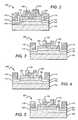
- FIGS. 1 a - 1 hshow an embodiment of a transistor device 100 in various stages of the fabrication process.
- a substrate 102such as sapphire or silicon carbide (SiC), for example, is provided on which one or more epitaxial layers 104 are grown.
- Some embodiments of the inventionmay be particularly well-suited for use in nitride-based devices such as Group III-nitride based HEMTs.
- Group III-nitriderefers to those semiconducting compounds formed between nitrogen and the elements in Group III of the periodic table, usually aluminum (Al), gallium (Ga), and/or indium (In).
- the termalso refers to ternary and quaternary compounds, such as AlGaN, InGaN, and AlInGaN.
- the Group III elementscan combine with nitrogen to form binary (e.g., GaN), ternary (e.g., AlGaN and AlInN), and quaternary (e.g., AlInGaN) compounds.
- binarye.g., GaN
- ternarye.g., AlGaN and AlInN
- quaternarye.g., AlInGaN
- the transistor device 100is a gallium nitride high electron mobility transistor (GaN HEMT).
- the device 100may comprise a barrier layer 106 that is disposed on the epitaxial layers 104 as shown in FIG. 1 b .
- the barrier layer 106can be doped or undoped layers of Group III-nitride materials. Barrier layers are known in the art and may be grown on or as a part of the epitaxial structure.
- the barrier layer 106may be AlGaN or, in other embodiments, the barrier layer 106 may include multiple layers, such as an AlN layer and an AlGaN layer.
- a regrowth mask 108is disposed on the barrier layer 106 as shown in FIG. 1 c.
- the regrowth mask materialis chosen and is deposited and selectively removed in such a way that it can function as a passivation layer on the semiconductor surface of the device 100 .
- Silicon nitride (SiN)may be used as the regrowth mask material.
- the regrowth mask 108is deposited on the surface of the epitaxial structure, in this embodiment, the barrier layer 106 .
- the regrowth mask 108can be deposited either in-situ after the growth of the layers 104 , 106 in an MOCVD reactor, or it can be deposited ex-situ in a high-temperature CVD system as long as the mask is of sufficient quality.
- the device 100can be patterned using a photoresist.
- portions of the regrowth mask 108 , and optionally portions of the barrier layer 106 and the epitaxial layers 104are then removed by etching, for example. Other methods of removal may also be used.
- the materialsmay be removed to various depths within the barrier layer 106 and the epitaxial layers 104 , with an acceptable depth being approximately 5 nm-1000 nm past the surface of the top semiconductor layer, in this case the barrier layer 106 .
- the removed portionsdefine regrowth areas.
- the portion of the regrowth mask that is leftconstitutes a regrowth mask residual layer 110 that remains on the device 100 during subsequent fabrication processes.
- Highly-doped semiconductor materialsare then grown in the regrowth areas, forming regrowth structures 112 that contact the epitaxial layers 104 and/or the barrier layer 106 as shown in FIG. 1 e .
- the highly-doped semiconductor materialsonly deposit in those areas not covered by the regrowth mask residual layer 110 .
- the highly-doped semiconductor materialcan be n + GaN.
- the regrowth structures 112may also comprise other materials as discussed below.
- An acceptable thickness for the regrowth structures 112is approximately 5 nm-500 nm.
- the local deposited thickness of the regrowth structures 112may be thicker in certain areas, especially near the edge of the regrowth mask residual layer 110 .
- a contact metalis deposited on the regrowth structures 112 , forming a drain contact 114 and a source contact 116 .
- the high doping density of the regrowth structures 112ensures that a low contact resistance can be achieved without annealing the contacts 114 , 116 at high temperatures.
- some materialis removed from the regrowth mask residual layer 110 to define a gate trench 118 .
- the materialmay be removed by etching, for example.
- a gate contact 120is then deposited in the gate trench 118 and on surrounding portions of regrowth mask residual layer 110 . It may also be desirable to deposit the drain, source and gate contacts 114 , 116 , 120 in a single step, thereby eliminating one of the lithography/deposition steps in the process if either low-temperature annealing or no annealing of the ohmic contact is done.
- FIG. 2shows another embodiment of a transistor device 200 .
- the device 200is similar to the device 100 and has several elements in common as indicated by common reference numbers.
- the device 200features a field plate 202 .
- the field plate 202can help to reduce the electric field within the device 200 . This helps to diminish component degradation due to spatially confined spikes in the electric field within the device 200 .
- the field plate 202is disposed on a spacer layer 204 .
- the spacer layer 204is deposited such that it at least partially covers the gate 120 and the regrowth mask residual layer 110 between the drain and source contacts 114 , 116 .
- the spacer layer 204can comprise a dielectric or another non-conductive material. As shown, the spacer layer may cover a portion of the drain and source contacts 114 , 116 .
- the field plate 202at least partially overlaps the gate contact 120 and extends toward the drain contact 114 . It is understood, however, that many different field plate shapes and configurations may be used. For example, a field plate may be connected to the source through an internal or external conductive path. It is also possible to include additional field plates separated by additional spacer layers.
- FIG. 3illustrates another embodiment of a transistor device 300 .
- the device 300is similar to the device 100 and comprises several common elements as indicated by common reference numbers.
- the device 300features regrowth mask residual layer 302 formed from aluminum nitride (AlN).
- AlNaluminum nitride
- the AlN materialis deposited at a high temperature, either in-situ after the growth of the epitaxial layer in an MOCVD reactor or ex-situ in a high temperature CVD system. Similarly as described above, the AlN material is selectively removed by etching, for example.
- the portion of the AlN material that remainsforms the regrowth mask residual layer 302 which functions to passivate the surface of the device and isolate various elements within the device 300 .
- the devicecan include an additional spacer layer and field plates (not shown).
- FIG. 4shows another embodiment of a transistor device 400 .
- the device 400is similar to the device 100 and shares several common elements.
- the regrowth mask residual layer 402is formed from any non-conducting material that exhibits minimal degradation during the subsequent regrowth process. Furthermore, the regrowth structure material should not deposit on the regrowth mask during the process.
- the regrowth mask residual layer 402can be a dielectric material or an insulator, for example, and functions as a passivation layer and/or a spacer in the finished device 400 .
- FIG. 5shows an embodiment of a transistor device 500 .
- the device 500is similar to the device 100 and contains several common elements.
- the device 500features regrowth structures 502 that comprise heavily-doped aluminum gallium nitride (n + AlGaN), heavily-doped indium gallium nitride (n + InGaN), or a combination such as n + AlGaN/GaN or n + InGaN/GaN.
- the regrowth structures 502provide a low contact resistance that does not require annealing the contacts 114 , 116 at high temperatures.
- the present inventionhas been described in considerable detail with reference to certain embodiments thereof, other versions are possible.
- the various embodiments of the transistor devicecan include additional elements such as field plates, for example, as described above.
- the field plates and gatescan also have many different shapes and may be connected to the source contact in many different ways. Accordingly, the spirit and scope of the invention should not be limited to the embodiments of the invention described above.
Landscapes
- Junction Field-Effect Transistors (AREA)
Abstract
Description
This application claims the benefit of a provisional application (App. No. 60/872,308) which was filed on Nov. 11, 2006.
This invention was made with Government support under Contract No. 05-C-0226 awarded by the Office of Naval Research. The Government has certain rights in this invention.
1. Field of the Invention
This invention relates to transistors and more particularly to transistors and methods for making ohmic contact to a transistor incorporating selective area growth.
2. Description of the Related Art
Improvements in the manufacturing of AlGaN/GaN semiconductor materials have helped advance the development of AlGaN/GaN transistors, such as high electron mobility transistors (HEMTs) for high frequency, high temperature and high power applications. AlGaN/GaN has large bandgaps, high peak and saturation electron velocity values [B. Gelmont, K. Kim and M. Shur,Monte Carlo Simulation of Electron Transport in Gallium Nitride, J. Appl. Phys. 74, (1993), pp. 1818-1821]. AlGaN/GaN HEMTs can also have 2DEG sheet densities in excess of 1013cm-2 and relatively high electron mobility (up to 2019 cm2/Vs) [R. Gaska, et al.,Electron Transport in AlGaN—GaN Heterostructures Grown on6H—SiC Substrates,Appl. Phys. Lett. 72, (1998), pp. 707-709]. These characteristics allow AlGaN/GaN HEMTs to provide very high voltage and high power operation at RF, microwave and millimeter wave frequencies.
U.S. Pat. No. 5,192,987 to Khan et al. discloses GaN/AlGaN based HEMTs grown on a buffer and a substrate. Other AlGaN/GaN HEMTs and field effect transistors (FETs) have been described by Gaska et al.,High-Temperature Performance of AlGaN/GaN HFET's on SiC Substrates, IEEE Electron Device Letters, 18, (1997), pp. 492-494; and Wu et al. “High Al-content AlGaN/GaN HEMTs With Very High Performance”, IEDM-1999 Digest, pp. 925-927, Washington D.C., December 1999. Some of these devices have shown a gain-bandwidth product (fT) as high as 100 gigahertz (Lu et al. “AlGaN/GaN HEMTs on SiC With Over 100 GHz ft and Low Microwave Noise”, IEEE Transactions on Electron Devices, Vol. 48, No. 3, March 2001, pp. 581-585) and high power densities up to 10 W/mm at X-band (Wu et al., “Bias-dependent Performance of High-Power AlGaN/GaN HEMTs”, IEDM-2001, Washington D.C., Dec. 2-6, 2001).
Field plates have been used to enhance the performance of GaN-based HEMTs [See S Kamalkar and U. K. Mishra,Very High Voltage AlGaN/GaN High Electron Mobility Transistors Using a Field Plate Deposited on a Stepped Insulator, Solid State Electronics 45, (2001), pp. 1645-1662]. Recently, field plate optimization for operation at microwave frequencies has resulted in drastically improved power densities exceeding 30 W/mm at 4 and 8 GHz [Wu et al, 30 W/mm GaN HEMTs by field plate optimization, IEEE Electron Device Letters, Vol. 25, No. 3, March 2004]. However, the reliability of these devices is still an issue, especially at high operation temperatures.
In present technology, ohmic contacts to GaN HEMTs are typically formed by alloying metal contacts at high temperature. This process results in ohmic contacts with rough morphology, which is undesirable for reliable devices and robust manufacturing. Furthermore, it has been proposed that alloying causes metal spiking into the semiconductor reducing the breakdown voltage of the device.
A typical prior art process for forming ohmic contacts on GaN HEMTs consists of depositing Ti/Al/Ni/Au or other similar metals on the semiconductor surface and then alloying the metals at a high temperature (>800° C.). This process results in ohmic contacts with rough morphology and a reduction in device breakdown voltage due to the spiking of the ohmic metal into the semiconductor.
Some technologies for non-annealed or low-temperature annealed ohmic contacts exist. These technologies include Si implants under the ohmic contacts, n+ GaN caps on top of the AlGaN/GaN structure, and selective area growth of n+ GaN in the contact region. These technologies, however, add complications to the process. In some of these prior art processes the regrowth mask is removed after the regrowth is performed. The mask removal can be difficult, leaving mask residue on the semiconductor surface. This problem can be exacerbated by a change in density or recrystallization of the regrowth mask during the high temperature regrowth stage.
One embodiment of a transistor device according to the present invention comprises at least one semiconductor layer. A regrowth mask residual layer is disposed on the at least one semiconductor layer. The regrowth mask residual layer has a gate trench. The device also includes a plurality of regrowth structures, each comprising a highly-doped semiconductor material. The regrowth structures contact respective portions of the at least one semiconductor layer. A drain contact and a source contact are each disposed on a different one of the regrowth structures. A gate is disposed on the regrowth mask residual layer and contacts the barrier layer through the gate trench.
One embodiment of a gallium nitride high electron mobility transistor (GaN HEMT) device according to the present invention comprises a plurality of semiconductor layers. A regrowth mask residual layer covers at least a portion of the plurality of semiconductor layers. A gate is disposed on the regrowth mask residual layer and contacts the plurality of semiconductor layers through a gate trench in the regrowth mask residual layer. A plurality of regrowth structures is disposed on the plurality of semiconductor layers. A source contact is disposed such that one of the regrowth structures is interposed between the source contact and the plurality of semiconductor layers. A drain contact is disposed such that one of the regrowth structures is interposed between the drain contact and the plurality of semiconductor layers.
An embodiment of a method for manufacturing a transistor device comprises growing a plurality of semiconductor layers on a substrate. A regrowth mask is formed on the plurality of semiconductor layers. Selected areas of the regrowth mask are removed such that portions of the plurality of semiconductor layers beneath the regrowth mask are also removed, leaving a regrowth mask residual layer to remain. Highly doped n-type regions are grown in the selected areas where the regrowth mask has been removed. Contact metals are deposited on the highly doped n-type regions. Material is removed from said regrowth mask residual layer to define a gate trench. Then, a gate is deposited on the regrowth mask residual layer and in the gate trench such that the gate contacts the plurality of semiconductor layers.
The present invention as disclosed in the claims enables low contact resistance as well as good morphology in the ohmic contacts without the use of high temperature annealing processes. This results in an ohmic contact fabrication process that does not require high temperature annealing or any annealing at all of the ohmic contact metals. One embodiment of a device according to the present invention relies on selective area growth wherein the regrowth mask material is chosen, and is deposited, in such a way that it can serve as a passivation and/or spacer element on the semiconductor surface in the final device structure. Thus, after the regrowth is performed, the regrowth mask is not removed, but stays on the semiconductor surface during the remainder of the device fabrication.
Embodiments of the invention are generally directed to transistors and in particular Group-III nitride HEMT devices, in which the ohmic contacts are non-alloyed. Although embodiments of the present invention are applicable to many different devices, they are particularly applicable to microwave and millimeter power GaN transistors and high-voltage switching GaN transistors.
The present invention is described herein with reference to certain embodiments, but it is understood that the invention can be embodied in many different forms and should not be construed as limited to the embodiments set forth herein.
It is also understood that when an element such as a layer, region or substrate is referred to as being “on” another element, it can be directly on the other element or intervening elements may also be present. Furthermore, relative terms such as. “inner”, “outer”, “upper”, “above”, “lower”, “beneath”, and “below”, and similar terms, may be used herein to describe a relationship of one layer or another region. It is understood that these terms are intended to encompass different orientations of the device in addition to the orientation depicted in the figures.
Although the terms first, second, etc. may be used herein to describe various elements, components, regions, layers and/or sections, these elements, components, regions, layers and/or sections should not be limited by these terms. These terms are only used to distinguish one element, component, region, layer or section from another region, layer or section. Thus, a first element, component, region, layer or section discussed below could be termed a second element, component, region, layer or section without departing from the teachings of the present invention.
Embodiments of the invention are described herein with reference to cross-sectional view illustrations that are schematic illustrations of idealized embodiments of the invention. It is understood that many of the layers will have different relative thicknesses compared to those shown. Further, variations from the shapes of the illustrations as a result, for example, of manufacturing techniques and/or tolerances are expected. Embodiments of the invention should not be construed as limited to the particular shapes of the regions illustrated herein but are to include deviations in shapes that result, for example, from manufacturing. A region illustrated or described as square or rectangular will typically have rounded or curved features due to normal manufacturing tolerances. Thus, the regions illustrated in the figures are schematic in nature and their shapes are not intended to illustrate the precise shape of a region of a device and are not intended to limit the scope of the invention.
Thedevice 100 may comprise abarrier layer 106 that is disposed on theepitaxial layers 104 as shown inFIG. 1 b. Thebarrier layer 106 can be doped or undoped layers of Group III-nitride materials. Barrier layers are known in the art and may be grown on or as a part of the epitaxial structure. In a preferred embodiment, thebarrier layer 106 may be AlGaN or, in other embodiments, thebarrier layer 106 may include multiple layers, such as an AlN layer and an AlGaN layer.
In this embodiment, aregrowth mask 108 is disposed on thebarrier layer 106 as shown inFIG. 1 c.The regrowth mask material is chosen and is deposited and selectively removed in such a way that it can function as a passivation layer on the semiconductor surface of thedevice 100. Silicon nitride (SiN) may be used as the regrowth mask material. Initially, theregrowth mask 108 is deposited on the surface of the epitaxial structure, in this embodiment, thebarrier layer 106. Theregrowth mask 108 can be deposited either in-situ after the growth of thelayers
After deposition, thedevice 100 can be patterned using a photoresist. Referring toFIG. 1 d, portions of theregrowth mask 108, and optionally portions of thebarrier layer 106 and theepitaxial layers 104 are then removed by etching, for example. Other methods of removal may also be used. The materials may be removed to various depths within thebarrier layer 106 and theepitaxial layers 104, with an acceptable depth being approximately 5 nm-1000 nm past the surface of the top semiconductor layer, in this case thebarrier layer 106. The removed portions define regrowth areas. The portion of the regrowth mask that is left constitutes a regrowth maskresidual layer 110 that remains on thedevice 100 during subsequent fabrication processes.
Highly-doped semiconductor materials are then grown in the regrowth areas, formingregrowth structures 112 that contact theepitaxial layers 104 and/or thebarrier layer 106 as shown inFIG. 1 e. The highly-doped semiconductor materials only deposit in those areas not covered by the regrowth maskresidual layer 110. In a GaN HEMT device, the highly-doped semiconductor material can be n+ GaN. Theregrowth structures 112 may also comprise other materials as discussed below. An acceptable thickness for theregrowth structures 112 is approximately 5 nm-500 nm. The local deposited thickness of theregrowth structures 112 may be thicker in certain areas, especially near the edge of the regrowth maskresidual layer 110. Again, it is noted that the figures are not drawn to scale and thus, do not reflect the accurate spatial relationship of the elements to scale; however, the general relationship is conveyed.
Referring toFIG. 1 f, a contact metal is deposited on theregrowth structures 112, forming adrain contact 114 and asource contact 116. The high doping density of theregrowth structures 112 ensures that a low contact resistance can be achieved without annealing thecontacts
InFIGS. 1 gand1h, some material is removed from the regrowth maskresidual layer 110 to define agate trench 118. The material may be removed by etching, for example. Agate contact 120 is then deposited in thegate trench 118 and on surrounding portions of regrowth maskresidual layer 110. It may also be desirable to deposit the drain, source andgate contacts
In this particular embodiment, thefield plate 202 at least partially overlaps thegate contact 120 and extends toward thedrain contact 114. It is understood, however, that many different field plate shapes and configurations may be used. For example, a field plate may be connected to the source through an internal or external conductive path. It is also possible to include additional field plates separated by additional spacer layers.
Although the present invention has been described in considerable detail with reference to certain embodiments thereof, other versions are possible. The various embodiments of the transistor device can include additional elements such as field plates, for example, as described above. The field plates and gates can also have many different shapes and may be connected to the source contact in many different ways. Accordingly, the spirit and scope of the invention should not be limited to the embodiments of the invention described above.
Claims (37)
1. A transistor device, comprising:
at least one semiconductor layer;
a regrowth mask residual layer on at least a portion of said at least one semiconductor layer, said regrowth mask residual layer comprising a gate trench;
a plurality of regrowth structures comprising a highly doped semiconductor material, said regrowth structures on different portions of said at least one semiconductor layer than the portion covered by said regrowth mask residual layer, wherein a top surface of each of said regrowth structures is below a top surface of said at least one semiconductor layer, said regrowth structures on respective portions of said at least one semiconductor layer;
a drain contact and a source contact, each disposed on a different one of said regrowth structures;
a gate disposed on said regrowth mask residual layer and electrically coupled to said at least one semiconductor layer through said gate trench.
2. The transistor device ofclaim 1 , wherein said regrowth mask residual layer functions as a passivation layer.
3. The transistor device ofclaim 1 , wherein said at least one semiconductor layer comprises gallium nitride (GaN).
4. The transistor device ofclaim 1 , wherein said plurality of regrowth structures comprises highly doped gallium nitride (n+ GaN.)
5. The transistor device ofclaim 1 , wherein said transistor device comprises a high electron mobility transistor (HEMT).
6. The transistor device ofclaim 1 , wherein said regrowth structures contact said source and drain contacts such that an ohmic contact having a non-annealed morphology or a morphology consistent with low-temperature annealing is formed.
7. The transistor device ofclaim 1 , wherein said at least one semiconductor layer comprises a barrier layer below said regrowth mask residual layer.
8. The transistor device ofclaim 1 , further comprising a spacer layer on said regrowth mask residual layer and said gate.
9. The transistor device ofclaim 8 , further comprising a field plate disposed over said spacer layer.
10. The transistor device ofclaim 1 , wherein said regrowth mask residual layer comprises aluminum nitride (AlN).
11. The transistor device ofclaim 1 , said regrowth structures comprising highly-doped aluminum gallium nitride (n+ AlGaN).
12. The transistor device ofclaim 1 , said regrowth structures comprising highly-doped indium gallium nitride (n+ InGaN).
13. The transistor device ofclaim 1 , said regrowth structures comprising a highly-doped combination of gallium nitride and aluminum gallium nitride (n+ GaN/AlGaN).
14. The transistor device ofclaim 1 , said regrowth structures comprising a highly-doped combination of gallium nitride and indium gallium nitride (n+ GaN/InGaN).
15. A gallium nitride high electron mobility transistor (GaN HEMT) device, comprising:
a plurality of semiconductor layers;
a regrowth mask residual layer covering at least a portion of said plurality of semiconductor layers;
a gate on said regrowth mask residual layer and contacting said plurality of semiconductor layers through a gate trench in said regrowth mask residual layer;
a plurality of regrowth structures disposed on said plurality of semiconductor layers, said regrowth structures on different portions of said plurality of semiconductor layers than the portion covered by said regrowth mask residual layer, wherein a top surface of each of said regrowth structures is below a top surface of said plurality of semiconductor layers;
a source contact such that one of said regrowth structures is interposed between said source contact and said plurality of semiconductor layers; and
a drain contact such that one of said regrowth structures is interposed between said drain contact and said plurality of semiconductor layers.
16. The HEMT ofclaim 15 , further comprising:
a spacer layer on said plurality of semiconductor layers; and
a field plate on said spacer layer at least partially between said source contact and said drain contact.
17. The GaN HEMT ofclaim 15 , wherein said regrowth mask residual layer comprises aluminum nitride (AlN).
18. The GaN HEMT ofclaim 15 , wherein said regrowth mask residual layer functions as a passivation layer.
19. The GaN HEMT ofclaim 15 , wherein said plurality of regrowth structures comprises highly-doped gallium nitride (n+ GaN).
20. The GaN HEMT ofclaim 15 , wherein said plurality of regrowth structures comprises highly-doped aluminum gallium nitride (n+ AlGaN).
21. The GaN HEMT ofclaim 15 , wherein said plurality of regrowth structures comprises highly-doped indium gallium nitride (n+ InGaN).
22. The GaN HEMT ofclaim 15 , wherein said regrowth structures contact said source and drain contacts such that an ohmic contact having a non-annealed morphology or a morphology consistent with low-temperature annealing is formed.
23. The GaN HEMT ofclaim 15 , said regrowth structures comprising a highly-doped combination of gallium nitride and aluminum gallium nitride (n+ GaN/AlGaN).
24. The GaN HEMT ofclaim 15 , said regrowth structures comprising a highly-doped combination of gallium nitride and indium gallium nitride (n+ GaN/InGaN).
25. A transistor device comprising:
at least one semiconductor layer;
a regrowth mask residual layer on at least a portion of said at least one semiconductor layer;
at least two regrowth structures comprising a highly doped semiconductor material, said regrowth structures adjacent said at least one semiconductor layer, such that said regrowth structures are adjacent to different portions of said at least one semiconductor layer than the portion covered by said regrowth mask residual layer, wherein a top surface of each of said regrowth structures is below a top surface of said at least one semiconductor layer;
a drain contact and a source contact, each on a different one of said at least two regrowth structures; and
a gate on said regrowth mask residual layer and within a gate trench of said regrowth mask residual layer.
26. The transistor device ofclaim 25 , wherein said at least one semiconductor layer comprises gallium nitride (GaN).
27. The transistor device ofclaim 25 , wherein said at least two regrowth structures comprises highly doped gallium nitride (n+GaN).
28. The transistor device ofclaim 25 , wherein said at least two regrowth structures contact said source and drain contacts such that an ohmic contact having a non-annealed morphology or a morphology consistent with low-temperature annealing is formed.
29. The transistor device ofclaim 25 , said at least one semiconductor layer comprising a barrier layer on said regrowth mask residual layer.
30. The transistor device ofclaim 25 , further comprising a spacer layer on said regrowth mask residual layer and said gate.
31. The transistor device ofclaim 30 , further comprising a field plate on said spacer layer.
32. The transistor device ofclaim 25 , wherein said regrowth mask residual layer comprises aluminum nitride (ALN).
33. The transistor device ofclaim 25 , said at least two regrowth structures comprising highly-doped aluminum gallium nitride (n+ AlGaN).
34. The transistor device ofclaim 25 , said at least two regrowth structures comprising highly-doped indium gallium nitride (n+ InGaN).
35. The transistor device ofclaim 25 , said at least two regrowth structures comprising a highly-doped combination of gallium nitride and aluminum gallium nitride (n30 GaN/AlGaN).
36. The transistor device ofclaim 25 , said at least two regrowth structures comprising a highly-doped combination of gallium nitride and indium gallium nitride (n30 GaN/InGaN).
37. A transistor precursor structure, comprising:
at least one semiconductor layer;
a regrowth mask residual layer on a portion of said at least one semiconductor layer, said regrowth mask residual layer shaped to define a gate trench for deposition of a gate material, wherein a surface of said at least one semiconductor layer is exposed through said gate trench; and
a plurality of regrowth structures on said at least one semiconductor layer, said regrowth structures comprising exposed surfaces for deposition of drain and source contacts, said plurality of regrowth structures disposed on different portions of said at least one semiconductor layer than the portion covered by said regrowth mask residual layer, wherein a top surface of each of said regrowth structures is below a top surface of said at least one semiconductor layer.
Priority Applications (1)
| Application Number | Priority Date | Filing Date | Title |
|---|---|---|---|
| US11/904,064US8878245B2 (en) | 2006-11-30 | 2007-09-25 | Transistors and method for making ohmic contact to transistors |
Applications Claiming Priority (2)
| Application Number | Priority Date | Filing Date | Title |
|---|---|---|---|
| US87230806P | 2006-11-30 | 2006-11-30 | |
| US11/904,064US8878245B2 (en) | 2006-11-30 | 2007-09-25 | Transistors and method for making ohmic contact to transistors |
Publications (2)
| Publication Number | Publication Date |
|---|---|
| US20080128753A1 US20080128753A1 (en) | 2008-06-05 |
| US8878245B2true US8878245B2 (en) | 2014-11-04 |
Family
ID=39474696
Family Applications (1)
| Application Number | Title | Priority Date | Filing Date |
|---|---|---|---|
| US11/904,064ActiveUS8878245B2 (en) | 2006-11-30 | 2007-09-25 | Transistors and method for making ohmic contact to transistors |
Country Status (1)
| Country | Link |
|---|---|
| US (1) | US8878245B2 (en) |
Cited By (3)
| Publication number | Priority date | Publication date | Assignee | Title |
|---|---|---|---|---|
| US9543490B2 (en) | 2010-09-24 | 2017-01-10 | Seoul Semiconductor Co., Ltd. | Wafer-level light emitting diode package and method of fabricating the same |
| RU2610346C1 (en)* | 2015-12-21 | 2017-02-09 | Федеральное государственное бюджетное учреждение науки Институт сверхвысокочастотной полупроводниковой электроники Российской академии наук (ИСВЧПЭ РАН) | METHOD OF MAKING OHMIC CONTACTS FOR AlGaN/GaN NITRIDE HETEROSTRUCTURES |
| US10580929B2 (en) | 2016-03-30 | 2020-03-03 | Seoul Viosys Co., Ltd. | UV light emitting diode package and light emitting diode module having the same |
Families Citing this family (27)
| Publication number | Priority date | Publication date | Assignee | Title |
|---|---|---|---|---|
| JP2008311355A (en)* | 2007-06-13 | 2008-12-25 | Rohm Co Ltd | Nitride semiconductor element |
| US7875537B2 (en)* | 2007-08-29 | 2011-01-25 | Cree, Inc. | High temperature ion implantation of nitride based HEMTs |
| US8368100B2 (en)* | 2007-11-14 | 2013-02-05 | Cree, Inc. | Semiconductor light emitting diodes having reflective structures and methods of fabricating same |
| US8836351B2 (en)* | 2008-06-10 | 2014-09-16 | University Of Florida Research Foundation, Inc. | Chloride detection |
| US7985986B2 (en) | 2008-07-31 | 2011-07-26 | Cree, Inc. | Normally-off semiconductor devices |
| US9449833B1 (en) | 2010-06-02 | 2016-09-20 | Hrl Laboratories, Llc | Methods of fabricating self-aligned FETS using multiple sidewall spacers |
| US8686473B1 (en)* | 2010-06-02 | 2014-04-01 | Hrl Laboratories, Llc | Apparatus and method for reducing the interface resistance in GaN heterojunction FETs |
| US8946724B1 (en) | 2010-06-02 | 2015-02-03 | Hrl Laboratories, Llc | Monolithically integrated self-aligned GaN-HEMTs and Schottky diodes and method of fabricating the same |
| US8383471B1 (en) | 2011-04-11 | 2013-02-26 | Hrl Laboratories, Llc | Self aligned sidewall gate GaN HEMT |
| CN103620751B (en)* | 2011-07-12 | 2017-08-01 | 松下知识产权经营株式会社 | Nitride semiconductor device and manufacturing method thereof |
| KR20130008281A (en)* | 2011-07-12 | 2013-01-22 | 삼성전자주식회사 | Methods for manufacturing power devices |
| US10002957B2 (en)* | 2011-12-21 | 2018-06-19 | Power Integrations, Inc. | Shield wrap for a heterostructure field effect transistor |
| EP2817834B1 (en) | 2012-02-23 | 2020-07-15 | Sensor Electronic Technology Inc. | Ohmic contact to semiconductor |
| CN103928323A (en)* | 2014-03-21 | 2014-07-16 | 中国电子科技集团公司第十三研究所 | Method for reducing ohmic contact resistance of HEMT device |
| TWI573269B (en)* | 2015-01-21 | 2017-03-01 | 南臺科技大學 | Semiconductor device |
| US9941384B2 (en) | 2015-08-29 | 2018-04-10 | Taiwan Semiconductor Manufacturing Co., Ltd. | Semiconductor device and method for fabricating the same |
| US10170611B1 (en) | 2016-06-24 | 2019-01-01 | Hrl Laboratories, Llc | T-gate field effect transistor with non-linear channel layer and/or gate foot face |
| CN106783569A (en)* | 2016-12-27 | 2017-05-31 | 山东聚芯光电科技有限公司 | A kind of method for improving ohmic contact resistance |
| US10868162B1 (en) | 2018-08-31 | 2020-12-15 | Hrl Laboratories, Llc | Self-aligned gallium nitride FinFET and method of fabricating the same |
| IT201900019980A1 (en)* | 2019-10-29 | 2021-04-29 | St Microelectronics Srl | METHOD OF MANUFACTURING A PORT TERMINAL OF A HEMT DEVICE, AND A HEMT DEVICE |
| JP2021086852A (en) | 2019-11-25 | 2021-06-03 | 住友電気工業株式会社 | Method for manufacturing semiconductor device and semiconductor device |
| US12040368B2 (en) | 2020-11-30 | 2024-07-16 | Innoscience (suzhou) Semiconductor Co., Ltd. | Semiconductor device and manufacturing method thereof |
| CN114695521A (en)* | 2020-12-30 | 2022-07-01 | 西安电子科技大学 | Silicon-based gallium nitride high-power radio frequency device based on gold-free process and preparation method thereof |
| CN113113478B (en)* | 2021-03-01 | 2022-10-04 | 西安电子科技大学 | GaN-based radio frequency power device based on ohmic regrowth and preparation method thereof |
| KR20230006737A (en)* | 2021-07-02 | 2023-01-11 | 에스케이하이닉스 주식회사 | Manufacturing method of memory device using mask patterns |
| US12218202B2 (en)* | 2021-09-16 | 2025-02-04 | Wolfspeed, Inc. | Semiconductor device incorporating a substrate recess |
| CN117747642A (en)* | 2022-09-13 | 2024-03-22 | 华为技术有限公司 | Semiconductor device and preparation method thereof |
Citations (90)
| Publication number | Priority date | Publication date | Assignee | Title |
|---|---|---|---|---|
| JPS5742179A (en) | 1980-08-27 | 1982-03-09 | Nec Corp | Semiconductor device with recognition pattern |
| US4824767A (en) | 1986-01-09 | 1989-04-25 | Intel Corporation | Dual glass contact process |
| JPH0329532A (en) | 1989-06-27 | 1991-02-07 | Matsushita Electric Works Ltd | Power supply backup system for bus system |
| JPH04284620A (en) | 1991-03-13 | 1992-10-09 | Mitsubishi Electric Corp | Manufacture of semiconductor device |
| US5192987A (en) | 1991-05-17 | 1993-03-09 | Apa Optics, Inc. | High electron mobility transistor with GaN/Alx Ga1-x N heterojunctions |
| US5334865A (en)* | 1991-07-31 | 1994-08-02 | Allied-Signal Inc. | MODFET structure for threshold control |
| US5393990A (en) | 1989-04-04 | 1995-02-28 | Siemens Corporate Research, Inc. | HEMT structure |
| JPH07111544A (en) | 1993-10-13 | 1995-04-25 | Fujitsu Ltd | Information transfer display system |
| JPH07283140A (en) | 1994-04-05 | 1995-10-27 | Nippon Telegr & Teleph Corp <Ntt> | Active atom supply control method |
| US5500381A (en) | 1994-03-30 | 1996-03-19 | Nec Corporation | Fabrication method of field-effect transistor |
| JPH08111544A (en) | 1994-10-07 | 1996-04-30 | Sharp Corp | Semiconductor light emitting device |
| US5563079A (en) | 1992-06-09 | 1996-10-08 | Goldstar Co., Ltd. | Method of making a field effect transistor |
| JPH098403A (en) | 1995-06-15 | 1997-01-10 | Nichia Chem Ind Ltd | Nitride semiconductor device manufacturing method and nitride semiconductor device |
| US5712175A (en) | 1994-09-12 | 1998-01-27 | Murata Manufacturing Co., Ltd. | Method of making semiconductor device having a schottky gate electrode |
| JPH10189649A (en) | 1996-12-20 | 1998-07-21 | Sharp Corp | Compound semiconductor device and electrode forming method thereof |
| JPH10223901A (en) | 1996-12-04 | 1998-08-21 | Sony Corp | Field effect transistor and method of manufacturing the same |
| JPH11150298A (en) | 1997-11-14 | 1999-06-02 | Nichia Chem Ind Ltd | Gallium nitride semiconductor light-emitting element and light-receiving element |
| JPH11261052A (en) | 1998-03-09 | 1999-09-24 | Furukawa Electric Co Ltd:The | High mobility transistor |
| US5990531A (en)* | 1995-12-28 | 1999-11-23 | Philips Electronics N.A. Corporation | Methods of making high voltage GaN-AlN based semiconductor devices and semiconductor devices made |
| US6004881A (en) | 1997-04-24 | 1999-12-21 | The United States Of America As Represented By The Secretary Of The Air Force | Digital wet etching of semiconductor materials |
| WO2000004587A2 (en) | 1998-06-12 | 2000-01-27 | Cree, Inc. | Nitride based transistors on semi-insulating silicon carbide substrates |
| US6046464A (en) | 1995-03-29 | 2000-04-04 | North Carolina State University | Integrated heterostructures of group III-V nitride semiconductor materials including epitaxial ohmic contact comprising multiple quantum well |
| US6071780A (en) | 1996-09-19 | 2000-06-06 | Fujitsu Limited | Compound semiconductor apparatus and method for manufacturing the apparatus |
| JP2000174260A (en) | 1998-12-02 | 2000-06-23 | Fujitsu Ltd | Semiconductor device |
| JP2000311704A (en) | 1999-04-27 | 2000-11-07 | Toshiba Battery Co Ltd | Sealed nickel hydrogen secondary battery |
| JP2001007325A (en) | 1999-06-18 | 2001-01-12 | Sanyo Electric Co Ltd | Field-effect transistor |
| US6177685B1 (en) | 1998-01-20 | 2001-01-23 | Sharp Kabushiki Kaisha | Nitride-type III-V HEMT having an InN 2DEG channel layer |
| US6197609B1 (en) | 1998-09-07 | 2001-03-06 | Rohm Co., Ltd. | Method for manufacturing semiconductor light emitting device |
| JP2001077415A (en) | 1999-08-31 | 2001-03-23 | Sharp Corp | Manufacturing method of GaN-based compound semiconductor light emitting device |
| JP2001098369A (en) | 1999-09-29 | 2001-04-10 | Sanyo Shinku Kogyo Kk | Film forming method by sputtering, and its device |
| JP2001308380A (en) | 2000-04-19 | 2001-11-02 | Seiwa Electric Mfg Co Ltd | Gallium nitride semiconductor light-emitting element |
| US6316820B1 (en) | 1997-07-25 | 2001-11-13 | Hughes Electronics Corporation | Passivation layer and process for semiconductor devices |
| US20020017648A1 (en)* | 2000-06-29 | 2002-02-14 | Kensuke Kasahara | Semiconductor device |
| JP2002077353A (en) | 2000-08-25 | 2002-03-15 | Moriguchi:Kk | Structure for attachment of light-emitting device for communications equipment to communications equipment |
| JP2002353499A (en) | 2001-05-23 | 2002-12-06 | Hitachi Cable Ltd | Semiconductor light emitting device |
| US20030085409A1 (en) | 2001-11-02 | 2003-05-08 | Yu-Chen Shen | Indium gallium nitride separate confinement heterostructure light emitting devices |
| US6586813B2 (en)* | 2000-07-17 | 2003-07-01 | Fujitsu Quantum Devices Limited | High-speed compound semiconductor device operable at large output power with minimum leakage current |
| US20030218183A1 (en)* | 2001-12-06 | 2003-11-27 | Miroslav Micovic | High power-low noise microwave GaN heterojunction field effet transistor |
| TW564584B (en) | 2001-06-25 | 2003-12-01 | Toshiba Corp | Semiconductor light emitting device |
| JP2003347589A (en) | 2002-05-28 | 2003-12-05 | Matsushita Electric Works Ltd | Led chip |
| JP2004047988A (en) | 2002-06-13 | 2004-02-12 | Lumileds Lighting Us Llc | Contact scheme for large and small area semiconductor light emitting flip chip devices |
| US20040159865A1 (en) | 2000-05-10 | 2004-08-19 | Allen Scott T. | Methods of fabricating silicon carbide metal-semiconductor field effect transistors |
| JP2004266240A (en) | 2002-07-08 | 2004-09-24 | Nichia Chem Ind Ltd | Method for manufacturing nitride semiconductor device and nitride semiconductor device |
| US6869812B1 (en) | 2003-05-13 | 2005-03-22 | Heng Liu | High power AllnGaN based multi-chip light emitting diode |
| US6885036B2 (en) | 1999-12-01 | 2005-04-26 | Cree, Inc. | Scalable LED with improved current spreading structures |
| US6888171B2 (en) | 2000-12-22 | 2005-05-03 | Dallan Luming Science & Technology Group Co., Ltd. | Light emitting diode |
| JP2005123489A (en) | 2003-10-20 | 2005-05-12 | Nichia Chem Ind Ltd | Nitride semiconductor light emitting device and manufacturing method thereof |
| US20050173728A1 (en) | 2004-02-05 | 2005-08-11 | Saxler Adam W. | Nitride heterojunction transistors having charge-transfer induced energy barriers and methods of fabricating the same |
| JP2005244152A (en) | 2004-01-29 | 2005-09-08 | Kyocera Corp | Light emitting element mounting substrate and light emitting device |
| EP1577951A2 (en) | 2004-03-11 | 2005-09-21 | Kabushiki Kaisha Toshiba | A semiconductor device and method of its manufacture |
| US20050211989A1 (en) | 2004-03-29 | 2005-09-29 | Stanley Electric Co., Ltd. | Semiconductor light emitting device capable of suppressing silver migration of reflection film made of silver |
| US20050258431A1 (en)* | 2004-05-22 | 2005-11-24 | Smith Richard P | Dielectric passivation for semiconductor devices |
| US20050258451A1 (en)* | 2004-05-20 | 2005-11-24 | Saxler Adam W | Methods of fabricating nitride-based transistors having regrown ohmic contact regions and nitride-based transistors having regrown ohmic contact regions |
| US20050258450A1 (en)* | 2004-05-20 | 2005-11-24 | Saxler Adam W | Semiconductor devices having a hybrid channel layer, current aperture transistors and methods of fabricating same |
| WO2005114743A2 (en) | 2004-05-11 | 2005-12-01 | Cree, Inc. | Wide bandgap transistors with multiple field plates |
| US20060006414A1 (en)* | 2004-06-30 | 2006-01-12 | Marianne Germain | AlGaN/GaN high electron mobility transistor devices |
| WO2006006555A1 (en) | 2004-07-12 | 2006-01-19 | Rohm Co., Ltd. | Semiconductor light-emitting device |
| JP2006128727A (en) | 2003-05-27 | 2006-05-18 | Matsushita Electric Works Ltd | Semiconductor light-emitting element |
| US20060108606A1 (en)* | 2004-11-23 | 2006-05-25 | Saxler Adam W | Cap layers and/or passivation layers for nitride-based transistors, transistor structures and methods of fabricating same |
| TW200627675A (en) | 2004-09-23 | 2006-08-01 | Lumileds Lighting Llc | Growth of Ⅲ-nitride light-emitting devices on textured substrates |
| TW200627674A (en) | 2004-09-22 | 2006-08-01 | Cree Inc | High efficiency group Ⅲ nitride-silicon carbide light emitting diode |
| US20060202272A1 (en)* | 2005-03-11 | 2006-09-14 | Cree, Inc. | Wide bandgap transistors with gate-source field plates |
| JP2006313888A (en) | 2005-05-03 | 2006-11-16 | Samsung Electro Mech Co Ltd | Nitride-based semiconductor light-emitting device and manufacturing method thereof |
| JP2007031704A (en) | 2005-06-22 | 2007-02-08 | Sumitomo Chemical Co Ltd | Polymer material and polymer light emitting device |
| US20070063215A1 (en) | 2005-09-16 | 2007-03-22 | Rohm Co., Ltd. | Manufacturing method for nitride semiconductor device and nitride semiconductor light emitting device obtained with the same |
| JP2007073965A (en) | 2005-09-08 | 2007-03-22 | Samsung Electro Mech Co Ltd | Nitride semiconductor light emitting device and method for manufacturing nitride semiconductor light emitting device |
| US20070102715A1 (en) | 2005-11-07 | 2007-05-10 | Samsung Electro-Mechanics Co., Ltd. | Semiconductor light emitting device |
| US20070228415A1 (en) | 2006-03-30 | 2007-10-04 | Fujitsu Limited | Semiconductor device and manufacturing method thereof |
| WO2007141763A1 (en) | 2006-06-09 | 2007-12-13 | Koninklijke Philips Electronics N.V. | Low profile side emitting led |
| US20080064133A1 (en) | 2004-08-11 | 2008-03-13 | Samsung Electro-Mechanics., Ltd | Nitride semiconductor light emitting diode and method of manufacturing the same |
| EP1901342A1 (en) | 2005-06-10 | 2008-03-19 | NEC Corporation | Field effect transistor |
| EP1901341A1 (en) | 2005-06-10 | 2008-03-19 | NEC Corporation | Field effect transistor |
| US7365374B2 (en)* | 2005-05-03 | 2008-04-29 | Nitronex Corporation | Gallium nitride material structures including substrates and methods associated with the same |
| JP2008112957A (en) | 2006-10-06 | 2008-05-15 | Mitsubishi Cable Ind Ltd | GaN-BASED LED CHIP |
| US20080203541A1 (en) | 2007-02-22 | 2008-08-28 | Fujitsu Limited | Semiconductor device and manufacturing method of the same |
| US20080217635A1 (en) | 2004-06-30 | 2008-09-11 | David Todd Emerson | Light emitting devices having current reducing structures and methods of forming light emitting devices having current reducing structures |
| US20080230799A1 (en) | 2005-10-27 | 2008-09-25 | Lattice Power (Jiangxi) Corporation | Semiconductor Light-Emitting Device with Electrode for N-Polar Ingaain Surface |
| US20080241757A1 (en) | 2007-03-27 | 2008-10-02 | Dong Xu | Reproducible, high yield method for fabricating ultra-short T-gates on HFETs |
| US20080237640A1 (en) | 2007-03-29 | 2008-10-02 | The Regents Of The University Of California | N-face high electron mobility transistors with low buffer leakage and low parasitic resistance |
| US7439166B1 (en) | 2005-06-11 | 2008-10-21 | Hrl Laboratories, Llc | Method for producing tiered gate structure devices |
| US20080258270A1 (en)* | 2004-10-13 | 2008-10-23 | Commissariat A L'energie Atomique | Mgo-Based Coating for Electrically Insulating Semiconductive Substrates and Production Method Thereof |
| US20080290364A1 (en) | 2007-05-24 | 2008-11-27 | Toyoda Gosei Co., Ltd. | Semiconductor light-emitting element and a producing method thereof |
| JP2008288548A (en) | 2007-04-16 | 2008-11-27 | Toyoda Gosei Co Ltd | Semiconductor light emitting device |
| US20080308832A1 (en) | 2007-06-14 | 2008-12-18 | Epistar Corporation | Light-emitting device |
| JP2009049342A (en) | 2007-08-23 | 2009-03-05 | Toyoda Gosei Co Ltd | Light emitting device |
| WO2009039805A1 (en) | 2007-09-28 | 2009-04-02 | Osram Opto Semiconductors Gmbh | Opto-electronic component and method for the production thereof |
| US20090140272A1 (en) | 2007-12-03 | 2009-06-04 | Goldeneye, Inc. | Solid-state light source |
| JP4284620B2 (en) | 2004-12-27 | 2009-06-24 | ソニー株式会社 | Information processing apparatus and method, and program |
| US7608497B1 (en) | 2006-09-08 | 2009-10-27 | Ivan Milosavljevic | Passivated tiered gate structure transistor and fabrication method |
| US20090283787A1 (en) | 2007-11-14 | 2009-11-19 | Matthew Donofrio | Semiconductor light emitting diodes having reflective structures and methods of fabricating same |
Family Cites Families (4)
| Publication number | Priority date | Publication date | Assignee | Title |
|---|---|---|---|---|
| DE2755433C2 (en)* | 1977-12-13 | 1986-09-25 | Telefunken electronic GmbH, 7100 Heilbronn | Radiation-emitting semiconductor diode |
| US6885025B2 (en)* | 2003-07-10 | 2005-04-26 | Universal Display Corporation | Organic light emitting device structures for obtaining chromaticity stability |
| DE102005036572A1 (en)* | 2005-08-01 | 2007-02-08 | Scheidt & Bachmann Gmbh | A method of automatically determining the number of people and / or objects in a gate |
| US20080289364A1 (en)* | 2007-05-23 | 2008-11-27 | Pinkham Jr Daniel | Method and system for preheating glass batch or ingredient(s) |
- 2007
- 2007-09-25USUS11/904,064patent/US8878245B2/enactiveActive
Patent Citations (95)
| Publication number | Priority date | Publication date | Assignee | Title |
|---|---|---|---|---|
| JPS5742179A (en) | 1980-08-27 | 1982-03-09 | Nec Corp | Semiconductor device with recognition pattern |
| US4824767A (en) | 1986-01-09 | 1989-04-25 | Intel Corporation | Dual glass contact process |
| US5393990A (en) | 1989-04-04 | 1995-02-28 | Siemens Corporate Research, Inc. | HEMT structure |
| JPH0329532A (en) | 1989-06-27 | 1991-02-07 | Matsushita Electric Works Ltd | Power supply backup system for bus system |
| JPH04284620A (en) | 1991-03-13 | 1992-10-09 | Mitsubishi Electric Corp | Manufacture of semiconductor device |
| US5192987A (en) | 1991-05-17 | 1993-03-09 | Apa Optics, Inc. | High electron mobility transistor with GaN/Alx Ga1-x N heterojunctions |
| US5334865A (en)* | 1991-07-31 | 1994-08-02 | Allied-Signal Inc. | MODFET structure for threshold control |
| US5563079A (en) | 1992-06-09 | 1996-10-08 | Goldstar Co., Ltd. | Method of making a field effect transistor |
| JPH07111544A (en) | 1993-10-13 | 1995-04-25 | Fujitsu Ltd | Information transfer display system |
| US5500381A (en) | 1994-03-30 | 1996-03-19 | Nec Corporation | Fabrication method of field-effect transistor |
| JPH07283140A (en) | 1994-04-05 | 1995-10-27 | Nippon Telegr & Teleph Corp <Ntt> | Active atom supply control method |
| US5712175A (en) | 1994-09-12 | 1998-01-27 | Murata Manufacturing Co., Ltd. | Method of making semiconductor device having a schottky gate electrode |
| JPH08111544A (en) | 1994-10-07 | 1996-04-30 | Sharp Corp | Semiconductor light emitting device |
| US6046464A (en) | 1995-03-29 | 2000-04-04 | North Carolina State University | Integrated heterostructures of group III-V nitride semiconductor materials including epitaxial ohmic contact comprising multiple quantum well |
| JPH098403A (en) | 1995-06-15 | 1997-01-10 | Nichia Chem Ind Ltd | Nitride semiconductor device manufacturing method and nitride semiconductor device |
| US5990531A (en)* | 1995-12-28 | 1999-11-23 | Philips Electronics N.A. Corporation | Methods of making high voltage GaN-AlN based semiconductor devices and semiconductor devices made |
| US6071780A (en) | 1996-09-19 | 2000-06-06 | Fujitsu Limited | Compound semiconductor apparatus and method for manufacturing the apparatus |
| JPH10223901A (en) | 1996-12-04 | 1998-08-21 | Sony Corp | Field effect transistor and method of manufacturing the same |
| JPH10189649A (en) | 1996-12-20 | 1998-07-21 | Sharp Corp | Compound semiconductor device and electrode forming method thereof |
| US6004881A (en) | 1997-04-24 | 1999-12-21 | The United States Of America As Represented By The Secretary Of The Air Force | Digital wet etching of semiconductor materials |
| US6316820B1 (en) | 1997-07-25 | 2001-11-13 | Hughes Electronics Corporation | Passivation layer and process for semiconductor devices |
| JPH11150298A (en) | 1997-11-14 | 1999-06-02 | Nichia Chem Ind Ltd | Gallium nitride semiconductor light-emitting element and light-receiving element |
| US6177685B1 (en) | 1998-01-20 | 2001-01-23 | Sharp Kabushiki Kaisha | Nitride-type III-V HEMT having an InN 2DEG channel layer |
| JPH11261052A (en) | 1998-03-09 | 1999-09-24 | Furukawa Electric Co Ltd:The | High mobility transistor |
| WO2000004587A2 (en) | 1998-06-12 | 2000-01-27 | Cree, Inc. | Nitride based transistors on semi-insulating silicon carbide substrates |
| US6197609B1 (en) | 1998-09-07 | 2001-03-06 | Rohm Co., Ltd. | Method for manufacturing semiconductor light emitting device |
| JP2000174260A (en) | 1998-12-02 | 2000-06-23 | Fujitsu Ltd | Semiconductor device |
| JP2000311704A (en) | 1999-04-27 | 2000-11-07 | Toshiba Battery Co Ltd | Sealed nickel hydrogen secondary battery |
| JP2001007325A (en) | 1999-06-18 | 2001-01-12 | Sanyo Electric Co Ltd | Field-effect transistor |
| JP2001077415A (en) | 1999-08-31 | 2001-03-23 | Sharp Corp | Manufacturing method of GaN-based compound semiconductor light emitting device |
| JP2001098369A (en) | 1999-09-29 | 2001-04-10 | Sanyo Shinku Kogyo Kk | Film forming method by sputtering, and its device |
| US6885036B2 (en) | 1999-12-01 | 2005-04-26 | Cree, Inc. | Scalable LED with improved current spreading structures |
| JP2001308380A (en) | 2000-04-19 | 2001-11-02 | Seiwa Electric Mfg Co Ltd | Gallium nitride semiconductor light-emitting element |
| US20040159865A1 (en) | 2000-05-10 | 2004-08-19 | Allen Scott T. | Methods of fabricating silicon carbide metal-semiconductor field effect transistors |
| US20020017648A1 (en)* | 2000-06-29 | 2002-02-14 | Kensuke Kasahara | Semiconductor device |
| US6586813B2 (en)* | 2000-07-17 | 2003-07-01 | Fujitsu Quantum Devices Limited | High-speed compound semiconductor device operable at large output power with minimum leakage current |
| JP2002077353A (en) | 2000-08-25 | 2002-03-15 | Moriguchi:Kk | Structure for attachment of light-emitting device for communications equipment to communications equipment |
| US6888171B2 (en) | 2000-12-22 | 2005-05-03 | Dallan Luming Science & Technology Group Co., Ltd. | Light emitting diode |
| JP2002353499A (en) | 2001-05-23 | 2002-12-06 | Hitachi Cable Ltd | Semiconductor light emitting device |
| TW564584B (en) | 2001-06-25 | 2003-12-01 | Toshiba Corp | Semiconductor light emitting device |
| US20030085409A1 (en) | 2001-11-02 | 2003-05-08 | Yu-Chen Shen | Indium gallium nitride separate confinement heterostructure light emitting devices |
| US20030218183A1 (en)* | 2001-12-06 | 2003-11-27 | Miroslav Micovic | High power-low noise microwave GaN heterojunction field effet transistor |
| JP2003347589A (en) | 2002-05-28 | 2003-12-05 | Matsushita Electric Works Ltd | Led chip |
| JP2004047988A (en) | 2002-06-13 | 2004-02-12 | Lumileds Lighting Us Llc | Contact scheme for large and small area semiconductor light emitting flip chip devices |
| JP2004266240A (en) | 2002-07-08 | 2004-09-24 | Nichia Chem Ind Ltd | Method for manufacturing nitride semiconductor device and nitride semiconductor device |
| US6869812B1 (en) | 2003-05-13 | 2005-03-22 | Heng Liu | High power AllnGaN based multi-chip light emitting diode |
| JP2006128727A (en) | 2003-05-27 | 2006-05-18 | Matsushita Electric Works Ltd | Semiconductor light-emitting element |
| JP2005123489A (en) | 2003-10-20 | 2005-05-12 | Nichia Chem Ind Ltd | Nitride semiconductor light emitting device and manufacturing method thereof |
| JP2005244152A (en) | 2004-01-29 | 2005-09-08 | Kyocera Corp | Light emitting element mounting substrate and light emitting device |
| US20050173728A1 (en) | 2004-02-05 | 2005-08-11 | Saxler Adam W. | Nitride heterojunction transistors having charge-transfer induced energy barriers and methods of fabricating the same |
| EP1577951A2 (en) | 2004-03-11 | 2005-09-21 | Kabushiki Kaisha Toshiba | A semiconductor device and method of its manufacture |
| US20050211989A1 (en) | 2004-03-29 | 2005-09-29 | Stanley Electric Co., Ltd. | Semiconductor light emitting device capable of suppressing silver migration of reflection film made of silver |
| US7141825B2 (en) | 2004-03-29 | 2006-11-28 | Stanley Electric Co., Ltd. | Semiconductor light emitting device capable of suppressing silver migration of reflection film made of silver |
| WO2005114743A2 (en) | 2004-05-11 | 2005-12-01 | Cree, Inc. | Wide bandgap transistors with multiple field plates |
| US20050258451A1 (en)* | 2004-05-20 | 2005-11-24 | Saxler Adam W | Methods of fabricating nitride-based transistors having regrown ohmic contact regions and nitride-based transistors having regrown ohmic contact regions |
| US20050258450A1 (en)* | 2004-05-20 | 2005-11-24 | Saxler Adam W | Semiconductor devices having a hybrid channel layer, current aperture transistors and methods of fabricating same |
| US7432142B2 (en)* | 2004-05-20 | 2008-10-07 | Cree, Inc. | Methods of fabricating nitride-based transistors having regrown ohmic contact regions |
| US20050258431A1 (en)* | 2004-05-22 | 2005-11-24 | Smith Richard P | Dielectric passivation for semiconductor devices |
| US20080217635A1 (en) | 2004-06-30 | 2008-09-11 | David Todd Emerson | Light emitting devices having current reducing structures and methods of forming light emitting devices having current reducing structures |
| US20060006414A1 (en)* | 2004-06-30 | 2006-01-12 | Marianne Germain | AlGaN/GaN high electron mobility transistor devices |
| WO2006006555A1 (en) | 2004-07-12 | 2006-01-19 | Rohm Co., Ltd. | Semiconductor light-emitting device |
| US20060273335A1 (en) | 2004-07-12 | 2006-12-07 | Hirokazu Asahara | Semiconductor light emitting device |
| US20080064133A1 (en) | 2004-08-11 | 2008-03-13 | Samsung Electro-Mechanics., Ltd | Nitride semiconductor light emitting diode and method of manufacturing the same |
| TW200627674A (en) | 2004-09-22 | 2006-08-01 | Cree Inc | High efficiency group Ⅲ nitride-silicon carbide light emitting diode |
| TW200627675A (en) | 2004-09-23 | 2006-08-01 | Lumileds Lighting Llc | Growth of Ⅲ-nitride light-emitting devices on textured substrates |
| US20080258270A1 (en)* | 2004-10-13 | 2008-10-23 | Commissariat A L'energie Atomique | Mgo-Based Coating for Electrically Insulating Semiconductive Substrates and Production Method Thereof |
| US20060108606A1 (en)* | 2004-11-23 | 2006-05-25 | Saxler Adam W | Cap layers and/or passivation layers for nitride-based transistors, transistor structures and methods of fabricating same |
| JP4284620B2 (en) | 2004-12-27 | 2009-06-24 | ソニー株式会社 | Information processing apparatus and method, and program |
| US20060202272A1 (en)* | 2005-03-11 | 2006-09-14 | Cree, Inc. | Wide bandgap transistors with gate-source field plates |
| JP2006313888A (en) | 2005-05-03 | 2006-11-16 | Samsung Electro Mech Co Ltd | Nitride-based semiconductor light-emitting device and manufacturing method thereof |
| US7365374B2 (en)* | 2005-05-03 | 2008-04-29 | Nitronex Corporation | Gallium nitride material structures including substrates and methods associated with the same |
| EP1901341A1 (en) | 2005-06-10 | 2008-03-19 | NEC Corporation | Field effect transistor |
| EP1901342A1 (en) | 2005-06-10 | 2008-03-19 | NEC Corporation | Field effect transistor |
| US7439166B1 (en) | 2005-06-11 | 2008-10-21 | Hrl Laboratories, Llc | Method for producing tiered gate structure devices |
| JP2007031704A (en) | 2005-06-22 | 2007-02-08 | Sumitomo Chemical Co Ltd | Polymer material and polymer light emitting device |
| JP2007073965A (en) | 2005-09-08 | 2007-03-22 | Samsung Electro Mech Co Ltd | Nitride semiconductor light emitting device and method for manufacturing nitride semiconductor light emitting device |
| US20070063215A1 (en) | 2005-09-16 | 2007-03-22 | Rohm Co., Ltd. | Manufacturing method for nitride semiconductor device and nitride semiconductor light emitting device obtained with the same |
| US20080230799A1 (en) | 2005-10-27 | 2008-09-25 | Lattice Power (Jiangxi) Corporation | Semiconductor Light-Emitting Device with Electrode for N-Polar Ingaain Surface |
| US20070102715A1 (en) | 2005-11-07 | 2007-05-10 | Samsung Electro-Mechanics Co., Ltd. | Semiconductor light emitting device |
| US20070228415A1 (en) | 2006-03-30 | 2007-10-04 | Fujitsu Limited | Semiconductor device and manufacturing method thereof |
| WO2007141763A1 (en) | 2006-06-09 | 2007-12-13 | Koninklijke Philips Electronics N.V. | Low profile side emitting led |
| US7608497B1 (en) | 2006-09-08 | 2009-10-27 | Ivan Milosavljevic | Passivated tiered gate structure transistor and fabrication method |
| JP2008112957A (en) | 2006-10-06 | 2008-05-15 | Mitsubishi Cable Ind Ltd | GaN-BASED LED CHIP |
| US20080203541A1 (en) | 2007-02-22 | 2008-08-28 | Fujitsu Limited | Semiconductor device and manufacturing method of the same |
| US20080241757A1 (en) | 2007-03-27 | 2008-10-02 | Dong Xu | Reproducible, high yield method for fabricating ultra-short T-gates on HFETs |
| US20080237640A1 (en) | 2007-03-29 | 2008-10-02 | The Regents Of The University Of California | N-face high electron mobility transistors with low buffer leakage and low parasitic resistance |
| JP2008288548A (en) | 2007-04-16 | 2008-11-27 | Toyoda Gosei Co Ltd | Semiconductor light emitting device |
| US20080290364A1 (en) | 2007-05-24 | 2008-11-27 | Toyoda Gosei Co., Ltd. | Semiconductor light-emitting element and a producing method thereof |
| US20080308832A1 (en) | 2007-06-14 | 2008-12-18 | Epistar Corporation | Light-emitting device |
| JP2009049342A (en) | 2007-08-23 | 2009-03-05 | Toyoda Gosei Co Ltd | Light emitting device |
| WO2009039805A1 (en) | 2007-09-28 | 2009-04-02 | Osram Opto Semiconductors Gmbh | Opto-electronic component and method for the production thereof |
| DE102007046743A1 (en) | 2007-09-28 | 2009-04-02 | Osram Opto Semiconductors Gmbh | Optoelectronic component and method for its production |
| US20090283787A1 (en) | 2007-11-14 | 2009-11-19 | Matthew Donofrio | Semiconductor light emitting diodes having reflective structures and methods of fabricating same |
| US8368100B2 (en) | 2007-11-14 | 2013-02-05 | Cree, Inc. | Semiconductor light emitting diodes having reflective structures and methods of fabricating same |
| US20090140272A1 (en) | 2007-12-03 | 2009-06-04 | Goldeneye, Inc. | Solid-state light source |
Non-Patent Citations (91)
| Title |
|---|
| "Enhancement of Base Conductivity Via the Piezoelectric Effect in AlGaN/GaN HBTs", Asbeck et al., Aug. 18, 1999, Solid State Electronics 44 (2000) 211 219, pp. 211-219. |
| "New UV Light Emitter based on AlGaN Heterostructures with Graded Electron and Hole Injectors", Johnson et al., XP-002505432, Mat. Res. Soc. Symp. Proc. vol. 743, 2003, Materials Research Society, pp. 1.2.4.1-1.7.4.6. |
| "Polarization-Induced 3-Dimensional Electron Slabs in Graded AlGaN Layers", Simon et al., XP-002505433, Mater. Res. Soc. Symp. Proc. vol. 892, 2006 Materials Research Society,pp. 1-6. |
| (From related application) European Office Action, Patent Application No. 07253716.0 dated Jan. 26, 2010. |
| Decision of Dismissal of Amendment from Japanese Patent Appl. No. 2012-510802, dated Feb. 18, 2014. |
| Decision of Rejection (Summary) for counterpart Japanese Patent Application No. 2009-243337 dated Nov. 2, 2010. |
| Decision of Rejection from Japanese Patent Application No. 2009-132243, dated Oct. 2, 2012. |
| Examination Report from related European Patent Application No. 02769655.8-1235, Dated: Nov. 3, 2008. |
| Examination Report from related European Patent Application No. 06851411.6-2203, dated: Jan. 26, 2009. |
| Examination Report re European Application No. 02 792 174.1-1235, Dated Oct. 7, 2008. |
| Examination Report re related European Application No. 01 905 364.4, dated: Jun. 24, 2009. |
| Examiner's Report from Canadian Patent Application No. 2,447,058 dated Dec. 15, 2009. |
| Examiner's Report from related Canada Patent Application No. 2,399,547, Dated: Mar. 4, 2009. |
| Extended European Search Report, for related European Application No. 07253716.0, Dated: Jun. 25, 2009. |
| Extended Search Report for European Patent Application No. 10187940.1 dated Feb. 8, 2011. |
| Final Notice of Reasons for Rejection (Summary) for Japanese Patent Application No. 2003-535260 dated Nov. 2, 2010. |
| Final Notice of Reasons for Rejection (Summary) for Japanese Patent Application No. 2009-243336 dated Nov. 2, 2010. |
| Final Official Notice of Rejection from Japanese Patent Application No. 2003-535260 mailed Jun. 8, 2010. |
| First Examination Report from related European Patent Application No. 08250197.4, dated: Jul. 28, 2009. |
| First Office Action from Chinese Patent Appl. No. 201080026730.9, dated Oct. 23, 2013. |
| From related application: European Office Action, Patent Application No. 02769655.8 dated Mar. 3, 2010. |
| From related application: European Office Action, Patent Application No. 02792174.1 dated Mar. 8, 2010. |
| Gaska et al., "Electron Transport in AlGaN-GaN Heterostructures Grown on 6H-SiC Substrates", Applied Physics Letters, vol. 72, No. 6, Feb. 1998, pp. 707-709. |
| Gaska, "High-Temperature Performance of AlGaN/GaN HFEts on SiC Substrates", IEEE Electron Device Letters, vol. 18, No. 10, Oct. 1997, pp. 492-494. |
| Gelmont et al., "Monte Carlo Simulation of Electron Transport in Gallium Nitride", J. Applied Physics, vol. 74, No. 3, Aug. 1993, pp. 1818-1821. |
| Grundbacher et al., "Utilization of an Electron Beam Resist Process to Examine the Effects of Asymmetric Gate Recess on the Device Characteristics of AlGaAs/InGaAs PHEMT's." IEEE. vol. 44, No. 12, Dec. 1997. |
| IEEE Electron Device Letters, vol. 21, No. 2, Feb. 2000, pp. 63-65, "AlGaN/GaN Metal Oxide Semiconductor Heteroatructure Field Effect Transistor,", M. Asif Khan et al. |
| IEEE Electron Device Letters, vol. 21, No. 9, Sep. 2000, pp. 421-423, "High Breakdown GaN HEMT with Overlapping Gate Structure," N.-Q. Zhang et al. |
| International Search Report and Written Opinion for PCT/US2010/024980 mailed Oct. 6, 2010. |
| International Tilak, V., et al., "Effect of Passivation on A1GaN/GaN HEMT Device Performance", 2000IEEE International Symposium on Compound Semiconductors, Proceedings of the IEEE Twenty-Seventh Symposium on Compound Semiconductors (Cat. No. 00TH8498), 2000 IEEE International Symposium on Compound Semiconductors Proceedings of TH, 2000, p. 357-363, XP002239700, Piscataway, NJ, USA, IEEE, USA. |
| Interrogation from Japanese Patent Application No. 2009-132243, dated Apr. 23, 2013. |
| Interrogatory from Japanese Patent Appl. No. 2010-504160, dated Jul. 16, 2013. |
| Invitation to Submit Applicant's Opinion and Examiner's Report to the Board, in Japanese Patent Application No. 2002-590421, Appeal Filing No. 2009-000996 dated Oct. 12, 2010. |
| Japanese Patent Application Public Disclosure 2000-68498, Date: Mar. 3, 2000. |
| Japanese Patent Application Public Disclosure 2001-77353, dated Mar. 23, 2001. |
| Japanese Publication No. Hei 11-224881, Aug. 17, 1999, Compound Semiconductor Apparatus. |
| Karmalkar et al. "Very High Voltage AlGaN/GaN High Electron Mobility Transistors Using a Field Plate Deposited on a Stepped Insulator", Solid State Electronics 45 (2001) pp. 1645-1652. |
| Khan et al., "AlGaN/GaN Metal-Oxide-Semiconductor Heterostructure Field-Effect Transistors on SiC Substrates", Applied Physics Letters Vo. 77, No. 9, Aug. 2000, pp. 1339-1341. |
| Lu, W., et al., "P-Type SiGe Transistors with Low Gate Leakage Using SiN Gate Dielectric", IEEE Electron Device Letters, IEEE Inc., New York, US vol. 20, No. 10, Oct. 1999, pp. 514-516 (XP000890470). |
| Notice of Allowance from U.S. Appl. No. 12/012,376, dated: May 13, 2011. |
| Notice of Reasons for Rejection from Japanese Patent Appl. No. 2009-132243, dated Oct. 1, 2013. |
| Notice of Reasons for Rejection from Japanese Patent Application No. 2012-510802, dated May 21, 2013. |
| Notice of Reasons for Rejection, Japanese Patent Appl. No. 2009-132243, dated Dec. 16, 2011. |
| Office Action Dated Dec. 28, 2009 for Related U.S. Appl. No. 11/726,975. |
| Office Action for family related U.S. Appl. No. 11/356,791, dated: Sep. 2, 2008. |
| Office Action for family related U.S. Appl. No. 11/799,786, dated Sep. 8, 2008. |
| Office Action from Japanese Patent Appl. No. 2012-510802, dated Oct. 8, 2013. |
| Office Action from Taiwanese Patent Appl. No. 097114378, dated May 12, 2014. |
| Office Action from U.S. Appl. No. 11/356,791, dated: Apr. 7, 2010. |
| Office Action from U.S. Appl. No. 11/356,791, dated: Jun. 11, 2010. |
| Office Action from U.S. Appl. No. 11/738,171, dated Jun. 27, 2013. |
| Office Action from U.S. Appl. No. 12/012,376, dated: Dec. 3, 2010. |
| Office Action from U.S. Appl. No. 12/012,376, dated: Feb. 22, 2011. |
| Office Action from U.S. Appl. No. 12/012,376, dated: Jul. 8, 2010. |
| Office Action from U.S. Appl. No. 12/185,031, dated Jun. 12, 2012. |
| Office Action from U.S. Appl. No. 12/185,031, dated: Jun. 14, 2011. |
| Office Action from U.S. Appl. No. 12/432,478, dated Jul. 1, 2013. |
| Office Action from U.S. Appl. No. 12/432,478, dated Jun. 20, 2012. |
| Office Action from U.S. Appl. No. 12/432,478, dated: May 16, 2011. |
| Office Action from U.S. Appl. No. 12/432,478, dated: Nov. 17, 2010. |
| Office Action from U.S. Appl. No. 13/023,788, dated Jul. 2, 2013. |
| Office Action from U.S. Appl. No. 13/023,788, dated Mar. 12, 2013. |
| Official Notice of Rejection from Japanese Patent Application No. 2009-243336 mailed Jun. 8, 2010. |
| Official Notice of Rejection from Japanese Patent Application No. 2009-243337 mailed Jun. 8, 2010. |
| Official Rejection of Japanese Patent Application No. 2003-535260, dated: Jun. 19, 2009. |
| Okamoto Y. et al. "A 149W Recessed-Gate A1GaN/GaN FP-FET", Microwave Symposium Digest, vol. 3, Jun. 6, 2004, p. 1351-1354. |
| Patent Abstracts of Japan, Pub. 10-223901, Pub. Date: Aug. 21, 1998. |
| PCT Notification of Transmittal of International Preliminary Examination Report for related PCT Application No. PCT/US06/26405, dated: Jan. 20, 2010. |
| Preliminary Examination Report from Japanese Patent Appl. No. 2010-504160, dated Jun. 25, 2013. |
| Rejection Decision from Chinese Patent Appl. No. 200880020777.7, dated Jul. 3, 2013. |
| Related European Examination Report for European Patent Application No. 02769655.8, dated: Dec. 8, 2008. |
| Related Extended European Search Report re European Application No. 08250197.4-1235/1973163, Dated: Nov. 6, 0. |
| Related Office Action from Japanese Patent Office re Japanese Patent Application No. 2002-590421, dated: Oct. 21, 2008. |
| Response to OA from U.S. Appl. No. 12/185,031, filed Aug. 24, 2012. |
| Response to OA from U.S. Appl. No. 12/432,478, filed Aug. 17, 2012. |
| Response to OA from U.S. Appl. No. 13/023,788, filed Jun. 11, 2013. |
| Response to Office Action from U.S. Appl. No. 11/356,791, dated May 25, 2010. |
| Response to Office Action from U.S. Appl. No. 11/726,975, dated: Mar. 29, 2010. |
| Response to Office Action from U.S. Appl. No. 12/012,376, filed: Jan. 26, 2011. |
| Response to Office Action from U.S. Appl. No. 12/012,376, filed: Mar. 22, 2011. |
| Response to Office Action from U.S. Appl. No. 12/012,376, filed: Sep. 28, 2010. |
| Response to Office Action from U.S. Appl. No. 12/432,478, filed: Mar. 17, 2011. |
| Result of Examination for related Korean Application No. 10-2004-7001027, Dec. 15, 2009. |
| Second Office Action from Chinese Patent Appl. No. 201080026730.9 dated Apr. 9, 2014. |
| Second Office Action from related China Application No. 02818502.1., Dated: Feb. 19, 2009. |
| Wu et al. , "Bias-Dependent Performance of High-Power AlGaN/GaN HEMTs", IEDM-2001, Washington DC, Dec. 2-6 2001,pp. 378-380. |
| Wu et al."High A1-Content AlGaN/GaN HEMTs on SiC Substrates With Very-High Power Performance", IEEE 1999 Digest, pp. 925-927. |
| Wu Lu, "AlGaN/GaN HEMTs on SiC With Over 100 GHz fT and Low Microwave Noise", IEEE Transactions on Electron Devices, vol. 48, No. 3, Mar. 2001, pp. 581-585. |
| Wu, "30-W/mm GaN HEMTs by Field Plate Optimization", IEEE Electron Device Letters, vol. 25, No. 3, Mar. 2001, pp. 117-119. |
| Xing, "High Breakdown Voltage AlGaN-GaN HEMTs Achieved by Multiple Field Plates", IEEE Electron Device Letters,vol. 25, No. 4, Apr. 2004, pp. 161-163. |
| Zhang, N-Q, et al., "High Breakdown GaN HEMT with Overlapping Gate Structure", IEEE Electronc Device Letters, IEEE, Inc., New York, US, vol. 21, No. 9, Sep. 2000, pp. 373-375, XP000954354. |
Cited By (7)
| Publication number | Priority date | Publication date | Assignee | Title |
|---|---|---|---|---|
| US9543490B2 (en) | 2010-09-24 | 2017-01-10 | Seoul Semiconductor Co., Ltd. | Wafer-level light emitting diode package and method of fabricating the same |
| US9882102B2 (en) | 2010-09-24 | 2018-01-30 | Seoul Semiconductor Co., Ltd. | Wafer-level light emitting diode and wafer-level light emitting diode package |
| US10069048B2 (en) | 2010-09-24 | 2018-09-04 | Seoul Viosys Co., Ltd. | Wafer-level light emitting diode package and method of fabricating the same |
| US10879437B2 (en) | 2010-09-24 | 2020-12-29 | Seoul Semiconductor Co., Ltd. | Wafer-level light emitting diode package and method of fabricating the same |
| US10892386B2 (en) | 2010-09-24 | 2021-01-12 | Seoul Semiconductor Co., Ltd. | Wafer-level light emitting diode package and method of fabricating the same |
| RU2610346C1 (en)* | 2015-12-21 | 2017-02-09 | Федеральное государственное бюджетное учреждение науки Институт сверхвысокочастотной полупроводниковой электроники Российской академии наук (ИСВЧПЭ РАН) | METHOD OF MAKING OHMIC CONTACTS FOR AlGaN/GaN NITRIDE HETEROSTRUCTURES |
| US10580929B2 (en) | 2016-03-30 | 2020-03-03 | Seoul Viosys Co., Ltd. | UV light emitting diode package and light emitting diode module having the same |
Also Published As
| Publication number | Publication date |
|---|---|
| US20080128753A1 (en) | 2008-06-05 |
Similar Documents
| Publication | Publication Date | Title |
|---|---|---|
| US8878245B2 (en) | Transistors and method for making ohmic contact to transistors | |
| US8212290B2 (en) | High temperature performance capable gallium nitride transistor | |
| US10134867B2 (en) | Method for fabricating semiconductor device | |
| JP5105160B2 (en) | Transistor | |
| US7592211B2 (en) | Methods of fabricating transistors including supported gate electrodes | |
| US7709859B2 (en) | Cap layers including aluminum nitride for nitride-based transistors | |
| EP1817798B2 (en) | Cap layers and/or passivation layers for nitride-based transistors, transistor structures and methods of fabricating same | |
| JP5203220B2 (en) | Method of making a transistor with a supported gate electrode and associated device | |
| JP6124511B2 (en) | Wide band gap transistor including gate-source field plate | |
| KR101202497B1 (en) | Nitride-based transistors with a protective layer and a low-damage recess and methods of fabrication thereof | |
| US12009417B2 (en) | High electron mobility transistors having improved performance | |
| CA2536030A1 (en) | Wide bandgap transistor devices with field plates | |
| US20230378313A1 (en) | Manufacturing method of semiconductor device | |
| WO2024011609A1 (en) | Semiconductor device and method for manufacturing thereof | |
| WO2024108422A1 (en) | Nitride-based semiconductor device and method for manufacturing thereof |
Legal Events
| Date | Code | Title | Description |
|---|---|---|---|
| AS | Assignment | Owner name:CREE, INC., CALIFORNIA Free format text:ASSIGNMENT OF ASSIGNORS INTEREST;ASSIGNORS:PARIKH, PRIMIT;HEIKMAN, STEN;REEL/FRAME:020078/0191 Effective date:20071105 | |
| STCF | Information on status: patent grant | Free format text:PATENTED CASE | |
| CC | Certificate of correction | ||
| MAFP | Maintenance fee payment | Free format text:PAYMENT OF MAINTENANCE FEE, 4TH YEAR, LARGE ENTITY (ORIGINAL EVENT CODE: M1551) Year of fee payment:4 | |
| MAFP | Maintenance fee payment | Free format text:PAYMENT OF MAINTENANCE FEE, 8TH YEAR, LARGE ENTITY (ORIGINAL EVENT CODE: M1552); ENTITY STATUS OF PATENT OWNER: LARGE ENTITY Year of fee payment:8 | |
| AS | Assignment | Owner name:U.S. BANK TRUST COMPANY, NATIONAL ASSOCIATION, NORTH CAROLINA Free format text:SECURITY INTEREST;ASSIGNOR:WOLFSPEED, INC.;REEL/FRAME:064185/0755 Effective date:20230623 |