US8878217B2 - LED package with efficient, isolated thermal path - Google Patents
LED package with efficient, isolated thermal pathDownload PDFInfo
- Publication number
- US8878217B2 US8878217B2US13/616,759US201213616759AUS8878217B2US 8878217 B2US8878217 B2US 8878217B2US 201213616759 AUS201213616759 AUS 201213616759AUS 8878217 B2US8878217 B2US 8878217B2
- Authority
- US
- United States
- Prior art keywords
- thermal
- electrical
- thermal element
- providing
- electrical element
- Prior art date
- Legal status (The legal status is an assumption and is not a legal conclusion. Google has not performed a legal analysis and makes no representation as to the accuracy of the status listed.)
- Active
Links
Images


Classifications
- H—ELECTRICITY
- H01—ELECTRIC ELEMENTS
- H01L—SEMICONDUCTOR DEVICES NOT COVERED BY CLASS H10
- H01L25/00—Assemblies consisting of a plurality of semiconductor or other solid state devices
- H01L25/03—Assemblies consisting of a plurality of semiconductor or other solid state devices all the devices being of a type provided for in a single subclass of subclasses H10B, H10D, H10F, H10H, H10K or H10N, e.g. assemblies of rectifier diodes
- H01L25/04—Assemblies consisting of a plurality of semiconductor or other solid state devices all the devices being of a type provided for in a single subclass of subclasses H10B, H10D, H10F, H10H, H10K or H10N, e.g. assemblies of rectifier diodes the devices not having separate containers
- H01L25/075—Assemblies consisting of a plurality of semiconductor or other solid state devices all the devices being of a type provided for in a single subclass of subclasses H10B, H10D, H10F, H10H, H10K or H10N, e.g. assemblies of rectifier diodes the devices not having separate containers the devices being of a type provided for in group H10H20/00
- H01L25/0753—Assemblies consisting of a plurality of semiconductor or other solid state devices all the devices being of a type provided for in a single subclass of subclasses H10B, H10D, H10F, H10H, H10K or H10N, e.g. assemblies of rectifier diodes the devices not having separate containers the devices being of a type provided for in group H10H20/00 the devices being arranged next to each other
- H—ELECTRICITY
- H01—ELECTRIC ELEMENTS
- H01L—SEMICONDUCTOR DEVICES NOT COVERED BY CLASS H10
- H01L2224/00—Indexing scheme for arrangements for connecting or disconnecting semiconductor or solid-state bodies and methods related thereto as covered by H01L24/00
- H01L2224/01—Means for bonding being attached to, or being formed on, the surface to be connected, e.g. chip-to-package, die-attach, "first-level" interconnects; Manufacturing methods related thereto
- H01L2224/42—Wire connectors; Manufacturing methods related thereto
- H01L2224/47—Structure, shape, material or disposition of the wire connectors after the connecting process
- H01L2224/48—Structure, shape, material or disposition of the wire connectors after the connecting process of an individual wire connector
- H01L2224/4805—Shape
- H01L2224/4809—Loop shape
- H01L2224/48091—Arched
- H—ELECTRICITY
- H01—ELECTRIC ELEMENTS
- H01L—SEMICONDUCTOR DEVICES NOT COVERED BY CLASS H10
- H01L2224/00—Indexing scheme for arrangements for connecting or disconnecting semiconductor or solid-state bodies and methods related thereto as covered by H01L24/00
- H01L2224/01—Means for bonding being attached to, or being formed on, the surface to be connected, e.g. chip-to-package, die-attach, "first-level" interconnects; Manufacturing methods related thereto
- H01L2224/42—Wire connectors; Manufacturing methods related thereto
- H01L2224/47—Structure, shape, material or disposition of the wire connectors after the connecting process
- H01L2224/48—Structure, shape, material or disposition of the wire connectors after the connecting process of an individual wire connector
- H01L2224/481—Disposition
- H01L2224/48151—Connecting between a semiconductor or solid-state body and an item not being a semiconductor or solid-state body, e.g. chip-to-substrate, chip-to-passive
- H01L2224/48221—Connecting between a semiconductor or solid-state body and an item not being a semiconductor or solid-state body, e.g. chip-to-substrate, chip-to-passive the body and the item being stacked
- H01L2224/48245—Connecting between a semiconductor or solid-state body and an item not being a semiconductor or solid-state body, e.g. chip-to-substrate, chip-to-passive the body and the item being stacked the item being metallic
- H01L2224/48247—Connecting between a semiconductor or solid-state body and an item not being a semiconductor or solid-state body, e.g. chip-to-substrate, chip-to-passive the body and the item being stacked the item being metallic connecting the wire to a bond pad of the item
- H—ELECTRICITY
- H01—ELECTRIC ELEMENTS
- H01L—SEMICONDUCTOR DEVICES NOT COVERED BY CLASS H10
- H01L2924/00—Indexing scheme for arrangements or methods for connecting or disconnecting semiconductor or solid-state bodies as covered by H01L24/00
- H01L2924/0001—Technical content checked by a classifier
- H01L2924/00014—Technical content checked by a classifier the subject-matter covered by the group, the symbol of which is combined with the symbol of this group, being disclosed without further technical details
- H01L33/486—
- H01L33/642—
- H—ELECTRICITY
- H10—SEMICONDUCTOR DEVICES; ELECTRIC SOLID-STATE DEVICES NOT OTHERWISE PROVIDED FOR
- H10H—INORGANIC LIGHT-EMITTING SEMICONDUCTOR DEVICES HAVING POTENTIAL BARRIERS
- H10H20/00—Individual inorganic light-emitting semiconductor devices having potential barriers, e.g. light-emitting diodes [LED]
- H10H20/80—Constructional details
- H10H20/85—Packages
- H10H20/8506—Containers
- H—ELECTRICITY
- H10—SEMICONDUCTOR DEVICES; ELECTRIC SOLID-STATE DEVICES NOT OTHERWISE PROVIDED FOR
- H10H—INORGANIC LIGHT-EMITTING SEMICONDUCTOR DEVICES HAVING POTENTIAL BARRIERS
- H10H20/00—Individual inorganic light-emitting semiconductor devices having potential barriers, e.g. light-emitting diodes [LED]
- H10H20/80—Constructional details
- H10H20/85—Packages
- H10H20/858—Means for heat extraction or cooling
- H10H20/8582—Means for heat extraction or cooling characterised by their shape
Definitions
- the subject matter disclosed hereinrelates generally to packages for light emitting diodes (LEDs). More particularly, the subject matter disclosed herein relates to packages for LEDs that are low-cost and have an efficient, isolated thermal path.
- LEDslight emitting diodes
- SMD housingstypically feature an LED chip connected to multiple metal leads formed from a leadframe and can optionally comprise a heat slug.
- Current packagescomprise portions of the metal leads which extend outside of the package and protrude from one or more lateral sides of the body.
- the increased surface area of the extended leadsincrease the capacity of the LED package to dissipate heat, however, the extended leads increase the size of the LED package requiring a relatively large area on a circuit board. Circuit board area is a scarce and costly factor in many applications.
- the extended leadsrequire more metal during package fabrication which can increase overall package cost.
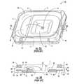
- a LED packagegenerally designated 10
- Body 12includes four lateral sides 1 - 4 , a bottom surface 5 , and a reflector cavity 14 .
- An encapsulant Efills the reflector cavity 14 to a desirable level, typically flush with the top of the reflector cavity.
- Encapsulant Etypically contains a phosphor for producing a desired wavelength spectrum.
- electrical componentstypically metal leads 16 and 18 formed from a leadframe, and to which one or more LED chips 20 are electrically connected.
- LED chips 20can optionally be mounted to a heat slug 22 which is electrically and thermally isolated from the metal leads 16 and 18 by insulating portions 24 and 26 , respectively, of the body 12 .
- Heat slug 22can improve thermal properties, including heat dissipation of LED package 10 .
- FIG. 1Bis a cross-sectional view along line 1 B in FIG. 1A .
- FIG. 1Billustrates body 12 which is molded about portions of metal leads 16 and 18 and portion of the heat slug 22 .
- External portions 28 and 30 of leads 16 and 18respectively, protrude from and extend away from lateral sides 4 and 2 and beyond the outermost edges of the body 12 .
- Metal leads 16 and 18are separated from the leadframe by terminating, such as by shearing, the external ends 34 and 36 of the leads 16 and 18 from the leadframe.
- External portions 28 and 30have a bend 32 which can configure the external portions 28 and 30 to extend away from each other and away from the body 12 .
- this designutilizes metal leads 16 and 18 which differ in thickness, and are typically thinner with a smaller cross-sectional area than the heat slug 22 .
- Heat slug 22protrudes from bottom surface 5 of the body 12 and metal leads 16 and 18 protrude from lateral sides 2 and 4 of the body 12 . All three of heat slug 22 and metal leads 16 and 18 become mounted to an external circuit source, generally a printed circuit board (PCB), at a location where they protrude from the body.
- PCBprinted circuit board
- heat slug 22comprises bottom surface 37 and metal leads 16 and 18 comprise bottom surfaces 38 and 39 , respectively.
- the metal leads 16 and 18have portions which are embedded on all four sides of the LED package 10 .
- metal leads 16 and 18can be embedded but extend from the body at external portions 28 and 30 on two opposing sides of LED package 10 , and can be embedded and flush with the remaining two opposing sides within the LED package 10 .
- the metal forming the metal leads 16 and 18is located on all four sides of the LED package 10 . Because the leads 16 and 18 contain portions 28 and 30 that extend from the body externally at lateral sides 2 and 4 , extra processing steps of bending the metal leads causes LED package 10 to have both an increased cost and a larger footprint than necessary thereby increasing the amount of space needed on a PCB.
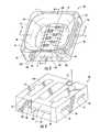
- this designfeatures an LED package generally designated 40 , having a body 42 with lateral sides 1 - 4 and a bottom surface 5 .
- This package designalso features a reflector cavity 44 configured for receiving a desirable level of encapsulant E.
- body 42is molded about a first metal lead 46 and a second metal lead 48 , wherein second metal lead 48 has a portion formed by stamping the metal to form a metal cup 50 .
- Metal cup 50forms metal walls about an inner bottom surface 51 a located or disposed on a lower and different plane P 2 than a surface of the body 42 forming one insulating portion 54 of the body which can be located or disposed on plane P 1 .
- Metal cup 50forms one electrical contact upon which one or more LED chips 52 are mounted. In addition to forming an electrical contact, cup 50 also serves as the thermal element, or heat slug, and is thereby neither electrically nor thermally isolated from both metal leads 46 and 48 . Cup 50 is thermally and electrically isolated from the first metal lead 46 by insulating portion 54 of the body. Cup 50 protrudes from bottom surface 5 of the body 42 to form an exposed portion 51 b while first and second metal leads 46 and 48 have external portions 56 and 58 , respectively which protrude from lateral sides 2 and 4 and extend beyond the outermost edges of the body 42 . The first and second metal leads 46 and 48 are separated from the leadframe by shearing the external ends 47 and 49 from the leadframe.
- the external portions 56 and 58 of first and second metal leads 46 and 48respectively, have external bends 60 and 62 which transition the external portions 56 and 58 to bend and/or wrap about body 42 such that they extend towards and face each other while also bending in towards metal cup 50 .
- External portions 56 and 58are disposed in recesses 64 and 66 of bottom surface 5 of body 42 to enable bottom surfaces 68 and 70 of external portions 56 and 58 to rest flush with and adjacent to the exposed portion 51 b of the metal cup 50 .
- These bottom surfacesare mounted to the PCB typically by using solder technology.
- the external sourcefor example the PCB will have to supply the isolation when connecting the LED package 10 components in series.
- first and second metal leads 46 and 48are thin and have a small cross-sectional area. For this reason, capacity of the metal leads to remove heat from the LED is limited. This limits the amount of power that can be sent to LED chips thereby limiting the amount of light that can be generated by the LED package.
- This designis similar to the design illustrated by FIGS. 1A and 1B as external portions 56 and 58 of first and second metal leads 46 and 48 thereby increases the footprint, includes a difficult bending step for the external portions, and increases the amount of metal necessary to fabricate the package which in turn increases cost and decreases space available on a PCB. In addition, this design utilizes metal leads 46 and 48 having portions which are embedded on all four sides of the LED package 40 .
- metal leads 46 and 48are embedded but extend from the body at external portions 56 and 58 on two opposing sides of LED package 40 , and are embedded and flush with the remaining two opposing sides within the LED package 40 .
- the metal forming the metal leads 46 and 48is located on all four sides of the LED package 40 .
- LED packagesare provided that can comprise a smaller footprint and single leadframe thickness while maintaining thermal isolation. It is, therefore, an object of the present disclosure herein to provide LED packages with improved cost and reduced footprint.
- FIG. 1Aillustrates a perspective top view of a LED package according to the prior art
- FIG. 1Billustrates a cross-sectional view of the LED package according to the prior art in FIG. 1A ;
- FIG. 2Aillustrates a perspective top view of a LED package according to the prior art
- FIG. 2Billustrates a cross-sectional view of the LED package according to the prior art in FIG. 2A ;
- FIG. 3illustrates a perspective top view of an embodiment of a LED package with electrical and thermal elements according to the subject matter herein;
- FIG. 4illustrates a perspective bottom view of the LED package according to the subject matter herein and in FIG. 3 ;
- FIG. 5illustrates a cross-sectional view of the LED package according to the subject matter herein and in FIG. 3 ;
- FIG. 6illustrates an opposing cross-sectional view of the LED package according to the subject matter herein and in FIG. 3 ;
- FIG. 7illustrates view of the LED package according to the subject matter herein.
- FIG. 8illustrates a perspective top view of an embodiment of a LED package with electrical and thermal elements according to the subject matter herein.
- references to a structure being formed “on” or “above” another structure or portioncontemplates that additional structure, portion, or both may intervene. References to a structure or a portion being formed “on” another structure or portion without an intervening structure or portion are described herein as being formed “directly on” the structure or portion.
- relative terms such as “on”, “above”, “upper”, “top”, “lower”, or “bottom”are used herein to describe one structure's or portion's relationship to another structure or portion as illustrated in the figures. It will be understood that relative terms such as “on”, “above”, “upper”, “top”, “lower” or “bottom” are intended to encompass different orientations of the device in addition to the orientation depicted in the figures. For example, if the device in the figures is turned over, structure or portion described as “above” other structures or portions would now be oriented “below” the other structures or portions. Likewise, if devices in the figures are rotated along an axis, structure or portion described as “above”, other structures or portions would now be oriented “next to” or “left of” the other structures or portions. Like numbers refer to like elements throughout.
- Light emitting devicesmay comprise III-V nitride (e.g., gallium nitride) based light emitting diodes (LEDs) or lasers fabricated on a silicon carbide substrate, such as those devices manufactured and sold by Cree, Inc. of Durham, N.C. Such LEDs and/or lasers may also be configured to operate such that light emission occurs through the substrate in a so-called “flip chip” orientation or by conventional wirebonding techniques.
- III-V nitridee.g., gallium nitride
- LEDslight emitting diodes
- lasersfabricated on a silicon carbide substrate, such as those devices manufactured and sold by Cree, Inc. of Durham, N.C.
- Cree, Inc. of Durham, N.CCree, Inc. of Durham, N.C.
- Such LEDs and/or lasersmay also be configured to operate such that light emission occurs through the substrate in a so-called “flip chip” orientation or by conventional wirebonding techniques.
- FIG. 3illustrates a top perspective view of one embodiment of a LED package, generally designated 80 .
- LED package 80can comprise a body 82 with four external lateral sides 71 - 74 , a top surface 84 a , and a bottom surface 84 b .
- Body 82can comprise any suitable material, for example ceramic, molded plastic, thermoset, or thermoplastic materials.
- Body 82can comprise a reflector cavity 86 for reflection of light thereby increasing light output, and reflector cavity 86 can be filled with a suitable level of encapsulant E producing a desired wavelength spectrum.
- encapsulant Eis filled to a level substantially flush with a top of reflector cavity 86 and flush with top surface 84 a of the body 82 although the level could be even with or above the top of reflector cavity 86 .
- a thermal element and at least one electrical elementcan lie along a bottom surface 85 of reflector cavity 86 .
- the thermal elementcan comprise a heat transfer material 88 , for example a heat slug.
- the electrical elementcan comprise one or more metal leads, for example metal leads 90 and 92 .
- Thermal transfer material 88can optionally be disposed between metal leads 90 and 92 , and can be thermally and electrically isolated from metal leads 90 and 92 by insulating portions 94 and 96 of molded body 82 which can form for example, during the molding process when molded material flows into divided areas between the thermal transfer material 88 and metal leads 90 and 92 .
- thermal transfer material 88 and metal leads 90 and 92can comprise any other suitable configuration other than having the thermal transfer material 88 disposed between metal leads 90 and 92 .
- Heat transfer material 88 and metal leads 90 and 92can thus have at least a portion of each embedded within body 82 .
- Body 82can further comprise one or more retaining notches 98 along one or more lateral sides, for example along opposing lateral sides 72 and 74 which can assist with and handling and placement of LED package 80 .
- retaining notches 98can provide areas which a leadframe having an array of package housings retains the housings in place until the appropriate time when the LED packages 80 are singulated.
- heat transfer material 88 and metal leads 90 and 92can extend directly from bottom surface 84 b of body 82 and can optionally be flush, or substantially flush, with bottom surface 84 b .
- heat transfer material 88 and metal leads 90 and 92can extend directly from bottom surface 84 b of body 82 and can extend lower than bottom surface 84 b , that is to a greater distance away from the body than bottom surface 84 b .
- Heat transfer material 88 and metal leads 90 and 92can have longitudinal axes that can be substantially parallel along an axis A-A of the LED package 80 .
- heat transfer material 88 and metal leads 90 and 92can be configured such that they can only extend directly from bottom surface 84 b and can be embedded, therefore can be in contact with, two opposing lateral sides of the LED package 80 .
- the metals forming metal leads 90 and 92are not embedded on all four lateral sides of the body as in the prior art, but rather are disposed between and have portions embedded in opposing lateral sides 71 and 73 .
- each component's respective perimeter, or footprintcan be surrounded and/or enclosed by bottom surface 84 b of the body 82 such that heat transfer material 88 and metal leads 90 and 92 do not extend to any significant degree or portion beyond outermost edges of lateral sides 71 - 74 of the body 82 . It is also possible though for metal leads 90 and 92 to extend from lateral sides 71 - 74 in another aspect, such as for example to form J-bend or gull-wing extensions in addition to extending directly from bottom surface 84 b .
- Heat transfer material 88can comprise exposed portions 100 that can be located or disposed along opposing lateral sides 71 and 73 , and optionally adjacent lateral sides 72 and 74 with retaining notches 98 .
- Retaining notches 98could also be disposed along opposing lateral sides 72 and 74 which contain the exposed portions 100 , 102 , and 104 .
- the exposed portion 100 of the thermal elementis on a lateral side that is orthogonal to longitudinal axis A.
- metal leads 90 and 92can comprise exposed portions 102 and 104 , respectively, which can be located or disposed along opposing lateral sides 71 and 73 .
- the exposed portions 102 and 104 of metal leads 90 and 92can also be disposed on a lateral side that is orthogonal to longitudinal axis A-A.
- Heat transfer material 88 and metal leads 90 and 92are positioned within the body 82 to extend between the respective exposed portions 100 , 102 , and 104 and are generally parallel.
- Exposed portions 100 , 102 , and 104can be located or disposed along a surface that is orthogonal to longitudinal axis A-A of the heat transfer material 88 , and metal leads 90 and 92 and can be separated and/or sheared from a leadframe such that they are at least substantially flush with lateral sides 71 and 73 .
- no significant portion of the thermal element 88 or metal leads 90 and 92extends beyond the outermost edges of lateral sides 71 - 74 of body 82 of LED package 80 . Separating and/or shearing can result in metal leads 90 and 92 at least substantially flush with opposing lateral sides 71 and 73 .
- heat transfer material 88can comprise a top surface 106 upon which one or more LED chips 108 can optionally become mounted ( FIG. 3 ). It is also contemplated in another aspect that one or more LED chips 108 can be thermally connected to heat transfer material 88 indirectly using another suitable configuration. For example, one or more intervening layers may be present between LED chips 108 and top surface 106 of heat transfer material 88 .
- Metal leads 90 and 92can comprise top surfaces 91 and 93 , respectively. Top surfaces 106 , 91 , and 93 can be flush with the bottom surface of the reflector cavity 85 which also comprises insulating portions 94 and 96 of the body.
- LED chips 108can electrically connect to the electrical elements, metal leads 90 and 92 through for example, conventional wirebonding.
- Heat transfer material 88can draw heat away from LED chips 108 and dissipate the heat from a bottom surface 107 of the heat transfer material 88 . Heat can travel from LED chip 108 and pass through the heat transfer material and along an isolated thermal path to an external source or substrate, for example a printed circuit board (PCB) or heat sink.
- FIG. 5is a view along 5 - 5 of FIG. 3 and illustrates heat transfer material 88 can be of a same or substantially same thickness as metal leads 90 and 92 .
- Metal leads 90 and 92 and heat transfer material 88can optionally have the respective bottom surfaces 110 , 112 , and 107 flush or substantially flush with bottom surface 84 b of LED package 80 .
- metal leads 90 and 92 and heat transfer material 88can optionally have the respective bottom surfaces 110 , 112 , and 107 located below bottom surface 84 b of the LED package 80 . That is, bottom surfaces 110 , 112 , and 107 extend from the body a greater distance than bottom surface 84 b .
- heat transfer material 88 and metal leads 90 and 92can comprise a same or substantially the same thickness and/or height within the body 82 .
- heat transfer material 88which can parallel metal leads 90 and 92 , can be stamped such that exposed portions 100 , 102 , and 104 are located and/or terminated at least substantially flush with the lateral edges 71 and 73 of LED package 80 such that no significant portion extends beyond outermost edges of LED package 80 .
- FIG. 6also illustrates bending portions 114 formed in heat transfer material 88 which can be embedded within body 82 and which are configured to transform the heat transfer material 88 from having top surface 106 that can be substantially flat along a plane P 4 to a second, embedded top surface 116 that also can be substantially flat and located or disposed along a parallel plane P 3 that can be located above plane P 4 .
- Heat transfer material 88can then terminate with exposed portions 100 substantially flush with lateral sides 71 and 73 and on a plane higher than top surface 106 .
- metal leads 90 and 92which can be parallel to heat transfer material 88 therefore, can also comprise bending portions which can transform the metal leads from top surfaces 91 and 93 along P 4 to a second, embedded surface along P 3 prior to terminating at exposed ends 102 and 104 which can be substantially flush with opposing lateral sides 71 and 73 .
- Heat transfer material 88 and metal leads 90 and 92are illustrated prior to embedding or molding within body 82 .
- Heat transfer material 88can be parallel with metal leads 90 and 92 , and comprise substantially similarly shaped cross-sections.
- heat transfer material 88can optionally be disposed between metal leads 90 and 92 and can comprise bending portions 114 .
- thermal transfer material 88 and metal leads 90 and 92can comprise any other suitable configuration other than having the thermal transfer material 88 disposed between metal leads 90 and 92 . As FIG.
- bending portions 114can be embedded within body 82 and configured to transform the heat transfer material 88 from having top surface 106 that can be substantially flat along a plane P 4 to a second, embedded top surface 116 that can be substantially flat and located or disposed along a parallel plane P 3 that can be located above and/or higher than plane P 4 .
- Heat transfer material 88can then terminate with exposed portions 100 at least substantially flush along opposing lateral sides of LED package 80 such that no significant portion of the heat transfer material 88 extends beyond the outermost edges of lateral sides 71 - 74 of the LED package 80 .
- metal leads 90 and 92can comprise bending portions 115 and 117 , respectively.
- the bending portions 115 and 117 of metal leads 90 and 92can be embedded within body 82 .
- Bending portions 115 and 117can be configured to transform the metal leads 90 and 92 from having top surfaces 91 and 93 which lie substantially flat along plane P 4 , to having second embedded top surfaces 118 and 119 , respectively, that can be substantially flat and located or disposed along a parallel plane P 3 that can be above and/or higher than plane P 4 .
- Metal leads 90 and 92can then terminate with exposed portions 102 and 104 , respectively, which can be at least substantially flush along opposing lateral sides of LED package 80 such that no significant portion of the metal leads 90 and 92 extends beyond the outermost edges of the lateral sides 71 - 74 of the LED package 80 .
- FIG. 8illustrates a perspective top view of an embodiment of a low-cost LED package, generally designated 120 having an isolated thermal path.
- LED package 120can comprise a body 122 with four external lateral sides 71 - 74 , a top surface 124 a , and a bottom surface 124 b .
- Body 122can comprise any suitable material known in the art for example ceramic, molded plastic, thermoset, or thermoplastic materials.
- Body 122can comprise a reflector cavity 126 for reflection of light thereby increasing light output.
- a lens 128can be formed, for example by molding lens 128 over the reflector cavity 126 and can be used for controlling optical properties such as, brightness and the focus.
- Lens 128can be generally convex but can comprise any suitable size and/or shape known in the art.
- Lens 128can optionally comprise a phosphor for obtaining a desired wavelength spectrum.
- a thermal element and at least one electrical elementcan lie along a bottom surface of reflector cavity 126 .
- the thermal elementcan comprise a heat transfer material 130 , for example a heat slug, upon which one or more LED chips 132 can be mounted. It is also contemplated in another aspect that one or more LED chips 132 can be thermally connected to heat transfer material 130 indirectly using another suitable configuration. For example, one or more intervening layers may be present between LED chips 108 and top surface 106 of heat transfer material 88 .
- the electrical elementcan comprise one or more metal leads, for example, metal leads 134 and 136 .
- Thermal transfer material 130can optionally be disposed between metal leads 134 and 136 and can be thermally and electrically isolated from metal leads 134 and 136 by insulating portions 94 and 96 of molded body 82 which can form for example, during the molding process when molded material flows into divided areas between the thermal transfer material 130 and metal leads 134 and 136 . It is also contemplated that in another aspect that thermal transfer material 130 and metal leads 134 and 136 can comprise any other suitable configuration other than having the thermal transfer material 130 disposed between metal leads 134 and 136 . Portions of heat transfer material 130 and metal leads 134 and 136 can thus be embedded within body 122 .
- Body 122further comprises one or more retaining notches 138 located along one or more lateral sides, for example along opposing lateral sides 72 and 74 which can assist with singulation of LED package 120 by providing areas which can retain an array of LED packages 120 and hold the packages together until the appropriate time.
- Heat transfer material 130 and metal leads 134 and 136terminate at exposed portions 140 , 142 , and 144 , respectively such that exposed portions 140 , 142 , and 144 are at least substantially flush with and do not have a significant portion extending beyond an outermost edge of the lateral sides 71 - 74 .
- Exposed portions 140 , 142 , and 144 of the heat transfer material 130 and metal leads 134 and 136terminate at opposing lateral sides, for example 71 and 73 .
- Heat transfer material 130 and metal leads 134 and 136can be generally parallel within body 122 .
- Bottom and cross-sectional views of this embodimentcan correspond in form and feature with those of FIGS. 4-7 and further comprise lens 128 about reflector cavity 126 .
- Lens 128can be formed integral with encapsulant E or as a separate portion.
- lens 128can comprise a separately formed glass portion having any size and/or shape which can optionally be disposed above the encapsulant E.
- lens 128can optionally comprise a single, molded lens comprising encapsulant E molded to form lens 128 of any size and/or shape about reflector cavity 126 of LED package 120 .
Landscapes
- Engineering & Computer Science (AREA)
- Power Engineering (AREA)
- Microelectronics & Electronic Packaging (AREA)
- Physics & Mathematics (AREA)
- Condensed Matter Physics & Semiconductors (AREA)
- General Physics & Mathematics (AREA)
- Computer Hardware Design (AREA)
- Led Device Packages (AREA)
Abstract
Description
Claims (51)
Priority Applications (1)
| Application Number | Priority Date | Filing Date | Title |
|---|---|---|---|
| US13/616,759US8878217B2 (en) | 2010-06-28 | 2012-09-14 | LED package with efficient, isolated thermal path |
Applications Claiming Priority (3)
| Application Number | Priority Date | Filing Date | Title |
|---|---|---|---|
| US12/825,075US8598602B2 (en) | 2009-01-12 | 2010-06-28 | Light emitting device packages with improved heat transfer |
| US12/853,812US8269244B2 (en) | 2010-06-28 | 2010-08-10 | LED package with efficient, isolated thermal path |
| US13/616,759US8878217B2 (en) | 2010-06-28 | 2012-09-14 | LED package with efficient, isolated thermal path |
Related Parent Applications (1)
| Application Number | Title | Priority Date | Filing Date |
|---|---|---|---|
| US12/853,812ContinuationUS8269244B2 (en) | 2010-06-28 | 2010-08-10 | LED package with efficient, isolated thermal path |
Publications (2)
| Publication Number | Publication Date |
|---|---|
| US20130011946A1 US20130011946A1 (en) | 2013-01-10 |
| US8878217B2true US8878217B2 (en) | 2014-11-04 |
Family
ID=45567898
Family Applications (2)
| Application Number | Title | Priority Date | Filing Date |
|---|---|---|---|
| US12/853,812ActiveUS8269244B2 (en) | 2010-06-28 | 2010-08-10 | LED package with efficient, isolated thermal path |
| US13/616,759ActiveUS8878217B2 (en) | 2010-06-28 | 2012-09-14 | LED package with efficient, isolated thermal path |
Family Applications Before (1)
| Application Number | Title | Priority Date | Filing Date |
|---|---|---|---|
| US12/853,812ActiveUS8269244B2 (en) | 2010-06-28 | 2010-08-10 | LED package with efficient, isolated thermal path |
Country Status (5)
| Country | Link |
|---|---|
| US (2) | US8269244B2 (en) |
| EP (1) | EP2603930A4 (en) |
| CN (2) | CN110071196A (en) |
| TW (1) | TWI515932B (en) |
| WO (1) | WO2012021238A1 (en) |
Cited By (4)
| Publication number | Priority date | Publication date | Assignee | Title |
|---|---|---|---|---|
| US9123874B2 (en) | 2009-01-12 | 2015-09-01 | Cree, Inc. | Light emitting device packages with improved heat transfer |
| US9859471B2 (en) | 2011-01-31 | 2018-01-02 | Cree, Inc. | High brightness light emitting diode (LED) packages, systems and methods with improved resin filling and high adhesion |
| US11101408B2 (en) | 2011-02-07 | 2021-08-24 | Creeled, Inc. | Components and methods for light emitting diode (LED) lighting |
| US11171273B2 (en) | 2014-12-30 | 2021-11-09 | Lumileds Llc | LED package with integrated features for gas or liquid cooling |
Families Citing this family (35)
| Publication number | Priority date | Publication date | Assignee | Title |
|---|---|---|---|---|
| US7923739B2 (en) | 2009-06-05 | 2011-04-12 | Cree, Inc. | Solid state lighting device |
| US9685592B2 (en) | 2009-01-14 | 2017-06-20 | Cree Huizhou Solid State Lighting Company Limited | Miniature surface mount device with large pin pads |
| US8686445B1 (en) | 2009-06-05 | 2014-04-01 | Cree, Inc. | Solid state lighting devices and methods |
| US8860043B2 (en)* | 2009-06-05 | 2014-10-14 | Cree, Inc. | Light emitting device packages, systems and methods |
| US9111778B2 (en) | 2009-06-05 | 2015-08-18 | Cree, Inc. | Light emitting diode (LED) devices, systems, and methods |
| US8648359B2 (en) | 2010-06-28 | 2014-02-11 | Cree, Inc. | Light emitting devices and methods |
| US8269244B2 (en)* | 2010-06-28 | 2012-09-18 | Cree, Inc. | LED package with efficient, isolated thermal path |
| USD643819S1 (en) | 2010-07-16 | 2011-08-23 | Cree, Inc. | Package for light emitting diode (LED) lighting |
| US8610140B2 (en) | 2010-12-15 | 2013-12-17 | Cree, Inc. | Light emitting diode (LED) packages, systems, devices and related methods |
| USD679842S1 (en) | 2011-01-03 | 2013-04-09 | Cree, Inc. | High brightness LED package |
| CN102934228B (en) | 2011-03-02 | 2017-09-01 | 惠州科锐半导体照明有限公司 | Light-emitting diode packages and light-emitting diodes |
| USD691100S1 (en)* | 2011-03-02 | 2013-10-08 | Cree Huizhou Solid State Lighting Company Limited | Miniature surface mount device |
| JP5456077B2 (en) | 2011-03-11 | 2014-03-26 | ソウル セミコンダクター カンパニー リミテッド | LED module, manufacturing method thereof, and LED channel letter including LED module |
| US10074779B2 (en)* | 2011-03-11 | 2018-09-11 | Seoul Semiconductor Co., Ltd. | LED module, method for manufacturing the same, and LED channel letter including the same |
| US8405181B2 (en)* | 2011-03-16 | 2013-03-26 | Intellectual Discovery Co., Ltd. | High brightness and high contrast plastic leaded chip carrier LED |
| USD676003S1 (en)* | 2011-08-29 | 2013-02-12 | Toyoda Gosei Co., Ltd. | Light emitting diode |
| US8692282B2 (en)* | 2011-10-27 | 2014-04-08 | Seoul Semiconductor Co., Ltd. | Light emitting diode package and light emitting module comprising the same |
| US8823041B2 (en) | 2011-10-27 | 2014-09-02 | Seoul Semiconductor Co., Ltd. | Light emitting diode package and light emitting module comprising the same |
| KR101197092B1 (en)* | 2011-11-24 | 2012-11-07 | 삼성전자주식회사 | Light emitting diode package and method for producting the light emitting diode package |
| TW201330332A (en)* | 2012-01-02 | 2013-07-16 | Lextar Electronics Corp | Solid state light emitting device and solid state light emitting package thereof |
| WO2013186653A1 (en)* | 2012-06-12 | 2013-12-19 | Koninklijke Philips N.V. | Lead frame light emitting arrangement |
| KR102042150B1 (en)* | 2012-09-13 | 2019-11-07 | 엘지이노텍 주식회사 | Light emitting device and lighting system |
| USD698742S1 (en)* | 2012-09-27 | 2014-02-04 | Kabushiki Kaisha Toshiba | Light-emitting diode |
| DE102013101262A1 (en) | 2013-02-08 | 2014-08-14 | Osram Opto Semiconductors Gmbh | Optoelectronic light module, optoelectronic light device and vehicle headlights |
| TWI598665B (en)* | 2013-03-15 | 2017-09-11 | 隆達電子股份有限公司 | Light-emitting element, long strip light-emitting element and application thereof |
| DE102013206225A1 (en) | 2013-04-09 | 2014-10-09 | Osram Opto Semiconductors Gmbh | Optoelectronic component and method for its production |
| US9461024B2 (en)* | 2013-08-01 | 2016-10-04 | Cree, Inc. | Light emitter devices and methods for light emitting diode (LED) chips |
| EP2908336A1 (en)* | 2014-02-17 | 2015-08-19 | Mitsubishi Electric R&D Centre Europe B.V. | A package of power dies |
| KR102161272B1 (en)* | 2014-03-25 | 2020-09-29 | 엘지이노텍 주식회사 | Light emitting device package |
| JP6398563B2 (en)* | 2014-05-29 | 2018-10-03 | 日亜化学工業株式会社 | Light emitting device |
| US9691949B2 (en) | 2014-05-30 | 2017-06-27 | Cree, Inc. | Submount based light emitter components and methods |
| JP6671117B2 (en)* | 2014-07-08 | 2020-03-25 | エルジー イノテック カンパニー リミテッド | Light emitting device package |
| CN108269762B (en)* | 2016-12-30 | 2021-06-08 | 联华电子股份有限公司 | Manufacturing method of semiconductor memory device |
| CN109904297A (en)* | 2017-12-11 | 2019-06-18 | 深圳市科纳实业有限公司 | Adopting surface mounted LED and products thereof and preparation method thereof |
| US10957736B2 (en) | 2018-03-12 | 2021-03-23 | Cree, Inc. | Light emitting diode (LED) components and methods |
Citations (137)
| Publication number | Priority date | Publication date | Assignee | Title |
|---|---|---|---|---|
| US4679118A (en) | 1984-08-07 | 1987-07-07 | Aavid Engineering, Inc. | Electronic chip-carrier heat sinks |
| US4946547A (en) | 1989-10-13 | 1990-08-07 | Cree Research, Inc. | Method of preparing silicon carbide surfaces for crystal growth |
| US5200022A (en) | 1990-10-03 | 1993-04-06 | Cree Research, Inc. | Method of improving mechanically prepared substrate surfaces of alpha silicon carbide for deposition of beta silicon carbide thereon and resulting product |
| US5210051A (en) | 1990-03-27 | 1993-05-11 | Cree Research, Inc. | High efficiency light emitting diodes from bipolar gallium nitride |
| USRE34861E (en) | 1987-10-26 | 1995-02-14 | North Carolina State University | Sublimation of silicon carbide to produce large, device quality single crystals of silicon carbide |
| US5393993A (en) | 1993-12-13 | 1995-02-28 | Cree Research, Inc. | Buffer structure between silicon carbide and gallium nitride and resulting semiconductor devices |
| US5506446A (en) | 1994-04-14 | 1996-04-09 | Olin Corporation | Electronic package having improved wire bonding capability |
| US5523589A (en) | 1994-09-20 | 1996-06-04 | Cree Research, Inc. | Vertical geometry light emitting diode with group III nitride active layer and extended lifetime |
| JP3154368B2 (en) | 1994-02-25 | 2001-04-09 | 新東工業株式会社 | Gas curing type mold making equipment |
| US6274924B1 (en) | 1998-11-05 | 2001-08-14 | Lumileds Lighting, U.S. Llc | Surface mountable LED package |
| US20010045640A1 (en) | 1997-02-10 | 2001-11-29 | Seishi Oida | Resin-molded semiconductor device and method for manufacturing the same |
| US20020004251A1 (en) | 1999-03-15 | 2002-01-10 | Roberts John K. | Method of making a semiconductor radiation emitter package |
| JP2002280616A (en) | 2001-03-16 | 2002-09-27 | Nichia Chem Ind Ltd | Package molding and light emitting device using the same |
| US6498355B1 (en)* | 2001-10-09 | 2002-12-24 | Lumileds Lighting, U.S., Llc | High flux LED array |
| US6610563B1 (en) | 1997-12-15 | 2003-08-26 | Osram Opto Semiconductors Gmbh & Co. Ohg | Surface mounting optoelectronic component and method for producing same |
| EP1242234B1 (en) | 1999-12-24 | 2003-10-08 | Gedib Ingenieurbüro Und Innovationsberatung Gmbh | Compressing device for performing compression operations on shaped bodies made of grainy materials |
| US20040075100A1 (en) | 2001-04-10 | 2004-04-22 | Georg Bogner | Leadframe and housing for radiation-emitting component, radiation-emitting component, and a method for producing the component |
| US20040079957A1 (en) | 2002-09-04 | 2004-04-29 | Andrews Peter Scott | Power surface mount light emitting die package |
| US20040126913A1 (en) | 2002-12-06 | 2004-07-01 | Loh Ban P. | Composite leadframe LED package and method of making the same |
| US6806583B2 (en) | 2000-06-28 | 2004-10-19 | Agilent Technologies, Inc. | Light source |
| JP2005179147A (en) | 2003-12-22 | 2005-07-07 | Matsushita Electric Works Ltd | Ceramic substrate for mounting photoelectric conversion element |
| JP2005209763A (en) | 2004-01-21 | 2005-08-04 | Nichia Chem Ind Ltd | LIGHT EMITTING DEVICE AND LIGHT EMITTING DEVICE MANUFACTURING METHOD |
| US6936855B1 (en) | 2002-01-16 | 2005-08-30 | Shane Harrah | Bendable high flux LED array |
| US6943433B2 (en) | 2002-03-06 | 2005-09-13 | Nichia Corporation | Semiconductor device and manufacturing method for same |
| US6949771B2 (en) | 2001-04-25 | 2005-09-27 | Agilent Technologies, Inc. | Light source |
| US20050269587A1 (en) | 2004-06-04 | 2005-12-08 | Loh Ban P | Power light emitting die package with reflecting lens and the method of making the same |
| USD514073S1 (en) | 2003-07-09 | 2006-01-31 | Nichai Corporation | Light emitting diode |
| US20060043401A1 (en) | 2004-09-01 | 2006-03-02 | Samsung Electro-Mechanics Co., Ltd. | High power light emitting diode package |
| WO2006059828A1 (en) | 2004-09-10 | 2006-06-08 | Seoul Semiconductor Co., Ltd. | Light emitting diode package having multiple molding resins |
| US20060118808A1 (en) | 2003-03-14 | 2006-06-08 | Sumitomo Electric Industries, Ltd. | Semiconductor device |
| KR100591687B1 (en) | 2005-05-06 | 2006-06-22 | 럭스피아 주식회사 | Multi-chip LED package with improved color scheme and backlight unit using the same |
| JP2006173561A (en) | 2004-12-16 | 2006-06-29 | Seoul Semiconductor Co Ltd | Lead frame having heat sink support ring, light emitting diode package manufacturing method using the same, and light emitting diode package manufactured using the same |
| US20060157726A1 (en) | 2005-01-14 | 2006-07-20 | Loh Ban P | Semiconductor light emitting device mounting substrates including a conductive lead extending therein and methods of packaging same |
| US7081661B2 (en) | 2001-03-16 | 2006-07-25 | Matsushita Electric Industrial Co., Ltd. | High-frequency module and method for manufacturing the same |
| US20060175716A1 (en) | 2003-06-20 | 2006-08-10 | Shintaro Nakashima | Molded package and semiconductor device using molded package |
| US20060186418A1 (en) | 2004-05-18 | 2006-08-24 | Edmond John A | External extraction light emitting diode based upon crystallographic faceted surfaces |
| WO2006095949A1 (en) | 2005-03-11 | 2006-09-14 | Seoul Semiconductor Co., Ltd. | Led package having an array of light emitting cells coupled in series |
| US20060220050A1 (en) | 2003-08-26 | 2006-10-05 | Sumitomo Electric Industries, Ltd. | Semiconductor light-emitting device mounting member, light-emitting diode constituting member using same, and light-emitting diode using same |
| KR20070000130U (en) | 2007-01-08 | 2007-01-26 | 김성우 | Air signboard with air conveying pipe |
| US20070052074A1 (en) | 2005-09-08 | 2007-03-08 | Sharp Kabushiki Kaisha | Optical coupling element, method for producing the optical coupling element, and electronic device equipped with the optical coupling element |
| US20070057364A1 (en) | 2005-09-01 | 2007-03-15 | Wang Carl B | Low temperature co-fired ceramic (LTCC) tape compositions, light emitting diode (LED) modules, lighting devices and method of forming thereof |
| US20070075325A1 (en) | 2005-10-04 | 2007-04-05 | Samsung Electro-Mechanics Co., Ltd. | High power light emitting diode package |
| JP2007108547A (en) | 2005-10-17 | 2007-04-26 | Hitachi Displays Ltd | Liquid crystal display |
| US20070114514A1 (en) | 2005-11-21 | 2007-05-24 | Sharp Kabushiki Kaisha | Light emitting device |
| US7224047B2 (en) | 2004-12-18 | 2007-05-29 | Lsi Corporation | Semiconductor device package with reduced leakage |
| US20070262328A1 (en) | 2006-05-10 | 2007-11-15 | Nichia Corporation | Semiconductor light emitting device and a method for producing the same |
| JP2007335762A (en) | 2006-06-16 | 2007-12-27 | Nichia Chem Ind Ltd | Light emitting device |
| WO2007126720A3 (en) | 2006-04-27 | 2008-01-03 | Cree Inc | Submounts for semiconductor light emitting device packages and semiconductor light emitting device packages including the same |
| US20080006837A1 (en) | 2006-07-07 | 2008-01-10 | Lg Electronics Inc. And Lg Innotek Co., Ltd | Sub-mount for mounting light emitting device and light emitting device package |
| US20080023722A1 (en) | 2006-07-28 | 2008-01-31 | Delta Electronics, Inc. | Light-emitting heat-dissipating device and packaging method thereof |
| WO2008021268A1 (en) | 2006-08-11 | 2008-02-21 | E. I. Du Pont De Nemours And Company | Led device and back panel of liquid crystal display |
| JP2008071954A (en) | 2006-09-14 | 2008-03-27 | Mimaki Denshi Buhin Kk | Light source device |
| USD566055S1 (en) | 2006-09-21 | 2008-04-08 | Lg Innotek Co., Ltd. | Light-emitting diode (LED) |
| JP2008091792A (en) | 2006-10-04 | 2008-04-17 | Nichia Chem Ind Ltd | Semiconductor device |
| CN201054361Y (en) | 2007-05-11 | 2008-04-30 | 凯鼎科技股份有限公司 | Light emitting diode |
| JP2008103480A (en) | 2006-10-18 | 2008-05-01 | Toyoda Gosei Co Ltd | Light-emitting device |
| WO2008069204A1 (en) | 2006-12-04 | 2008-06-12 | Alps Electric Co., Ltd. | Light emitting device and projector |
| JP2008147611A (en) | 2006-11-13 | 2008-06-26 | Nichia Chem Ind Ltd | Light emitting device |
| KR100845856B1 (en) | 2006-12-21 | 2008-07-14 | 엘지전자 주식회사 | Light emitting device package and its manufacturing method |
| USD573114S1 (en) | 2007-05-04 | 2008-07-15 | Samsung Electro-Mechanics Co., Ltd. | Light-emitting diode |
| US7400049B2 (en) | 2006-02-16 | 2008-07-15 | Stats Chippac Ltd. | Integrated circuit package system with heat sink |
| USD573113S1 (en) | 2005-12-09 | 2008-07-15 | Nichia Corporation | Light emitting diode |
| US20080185605A1 (en) | 2007-01-15 | 2008-08-07 | Citizen Electronics Co., Ltd. | Light-emitting diode and method for producing it |
| US7429790B2 (en) | 2005-10-24 | 2008-09-30 | Freescale Semiconductor, Inc. | Semiconductor structure and method of manufacture |
| US7432589B2 (en) | 2006-04-19 | 2008-10-07 | Nichia Corporation | Semiconductor device |
| US20080258130A1 (en) | 2007-04-23 | 2008-10-23 | Bergmann Michael J | Beveled LED Chip with Transparent Substrate |
| US20080258162A1 (en) | 2007-04-17 | 2008-10-23 | Koung Chia-Yin | Package for a high-power light emitting diode |
| USD580375S1 (en) | 2006-10-12 | 2008-11-11 | Semi-Photonics Co., Ltd. | Lead frame for a two-pin light emitting diode device |
| US20080278941A1 (en) | 2007-05-07 | 2008-11-13 | Philips Solid-State Lighting Solutions, Inc. | Led-based lighting fixtures for surface illumination with improved heat dissipation and manufacturability |
| USD580891S1 (en) | 2007-07-20 | 2008-11-18 | Alti-Electronics Co. Ltd. | Light emitting diode |
| US20080283849A1 (en) | 2007-05-16 | 2008-11-20 | Ushiodenki Kabushiki Kaisha | Led device and method by which it is produced |
| US20080290353A1 (en) | 2007-05-24 | 2008-11-27 | Medendorp Jr Nicholas W | Microscale optoelectronic device packages |
| JP2008545269A (en) | 2005-07-01 | 2008-12-11 | ラミナ ライティング インコーポレーテッド | LIGHTING DEVICE HAVING WHITE LIGHT EMITTING DIODE AND DIODE ARRAY, ITS MANUFACTURING METHOD AND MANUFACTURING DEVICE |
| US20090008662A1 (en) | 2007-07-05 | 2009-01-08 | Ian Ashdown | Lighting device package |
| KR20090003378A (en) | 2007-06-05 | 2009-01-12 | 주식회사 루멘스 | Light emitting diode package |
| JP2009016636A (en) | 2007-07-06 | 2009-01-22 | Nichia Corp | Semiconductor device and method for forming the same |
| US20090101921A1 (en) | 2007-10-17 | 2009-04-23 | Tai-Sol Electronics Co., Ltd. | LED and thermal conductivity device combination assembly |
| US20090122533A1 (en) | 2007-11-08 | 2009-05-14 | Innovations In Optics, Inc. | LED backlighting system with closed loop control |
| USD594827S1 (en) | 2006-12-07 | 2009-06-23 | Cree, Inc. | Lamp package |
| US20090159905A1 (en) | 2007-12-24 | 2009-06-25 | Kuei-Fang Chen | Light Emitting Assembly |
| USD595675S1 (en) | 2008-09-24 | 2009-07-07 | Harvatek Corporation | Light emitting diode |
| US7564180B2 (en) | 2005-01-10 | 2009-07-21 | Cree, Inc. | Light emission device and method utilizing multiple emitters and multiple phosphors |
| US7566159B2 (en) | 2007-05-31 | 2009-07-28 | Avago Technologies Ecbu Ip (Singapore) Pte. Ltd. | Side-emitting LED package with improved heat dissipation |
| US20090189178A1 (en) | 2006-06-30 | 2009-07-30 | Do Hyung Kim | Leadframe having a heat sink supporting part, fabricating method of a light emitting diode package using the same, and light emitting diode package fabricated by the method |
| USD597968S1 (en) | 2008-03-13 | 2009-08-11 | Rohm Co., Ltd. | Light emitting diode module |
| USD597971S1 (en) | 2008-03-13 | 2009-08-11 | Rohm Co., Ltd. | Light emitting diode module |
| US7592638B2 (en) | 2005-10-19 | 2009-09-22 | Lg Innotek Co., Ltd. | Light emitting diode package |
| US20090321779A1 (en) | 2005-11-25 | 2009-12-31 | Samsung Electro-Mechanics Co., Ltd. | Side view light emitting diode package |
| US7659551B2 (en) | 2003-05-27 | 2010-02-09 | Cree, Inc. | Power surface mount light emitting die package |
| JP2010034262A (en) | 2008-07-29 | 2010-02-12 | Sumitomo Metal Electronics Devices Inc | Light emitting element storage package |
| US20100059783A1 (en) | 2008-09-08 | 2010-03-11 | Harry Chandra | Light Emitting Chip Package With Metal Leads For Enhanced Heat Dissipation |
| TWM376909U (en) | 2009-09-28 | 2010-03-21 | Fu Sheng Ind Co Ltd | Frame structure for light emitting diodes |
| TW201013969A (en) | 2008-09-16 | 2010-04-01 | Upec Electronics Corp | Package structure of light-emitting diode |
| USD614592S1 (en) | 2008-08-28 | 2010-04-27 | Cree, Inc. | Light emitting diode |
| US20100102345A1 (en) | 2007-04-19 | 2010-04-29 | Lg Innotek Co., Ltd. | Light emitting device package and light unit having the same |
| USD615504S1 (en) | 2007-10-31 | 2010-05-11 | Cree, Inc. | Emitter package |
| US20100133554A1 (en) | 2009-06-05 | 2010-06-03 | Cree, Inc. | Solid state lighting device |
| US20100133578A1 (en) | 2009-08-04 | 2010-06-03 | Cree Led Lighting Solutions, Inc. | Solid state lighting device with improved heatsink |
| US20100155748A1 (en) | 2009-01-14 | 2010-06-24 | Cree Hong Kong Limited | Aligned multiple emitter package |
| US20100163887A1 (en) | 2008-12-31 | 2010-07-01 | Seoul Opto Device Co., Ltd. | Light emitting device having a plurality of non-polar light emitting cells and a method of fabricating the same |
| TWM383822U (en) | 2010-02-12 | 2010-07-01 | Bi Chi Corp | Light emitting diode base structure of free-bending swan neck |
| US20100181582A1 (en) | 2009-01-22 | 2010-07-22 | Intematix Corporation | Light emitting devices with phosphor wavelength conversion and methods of manufacture thereof |
| USD621798S1 (en) | 2008-08-29 | 2010-08-17 | Foxsemicon Integrated Technology, Inc. | Light-emitting diode substrate |
| USD621799S1 (en) | 2009-01-12 | 2010-08-17 | Cree, Inc. | Light emitting diode |
| USD622680S1 (en) | 2009-12-04 | 2010-08-31 | Silitek Electronic (Guangzhou) Go., Ltd. | Package of a light emitting diode |
| JP2010205776A (en) | 2009-02-27 | 2010-09-16 | Toshiba Lighting & Technology Corp | Light-emitting module |
| US20100237360A1 (en) | 2009-03-19 | 2010-09-23 | Chih-Chiang Kao | Light emitting diode and back light module thereof |
| USD626095S1 (en) | 2009-12-11 | 2010-10-26 | Everlight Electronics Co., Ltd. | Light emitting diode |
| US20100270577A1 (en) | 2007-07-23 | 2010-10-28 | Dsm Ip Assets B.V. | Plastic component for a lighting systems |
| USD627310S1 (en) | 2009-11-27 | 2010-11-16 | Lite-On Technology Corp. | Package of a light emitting diode |
| USD628541S1 (en) | 2010-06-14 | 2010-12-07 | Everlight Electronics Co., Ltd. | Light emitting diode |
| US7852015B1 (en) | 2006-10-11 | 2010-12-14 | SemiLEDs Optoelectronics Co., Ltd. | Solid state lighting system and maintenance method therein |
| US20110006658A1 (en) | 2009-07-07 | 2011-01-13 | Cree Led Lighting Solutions, Inc. | Solid state lighting device with improved heatsink |
| USD632267S1 (en) | 2010-02-12 | 2011-02-08 | Lextar Electronics Corp. | Light emitting diode packaging carrier |
| US20110031865A1 (en) | 2009-01-12 | 2011-02-10 | Hussell Christopher P | Light emitting device packages with improved heat transfer |
| USD632659S1 (en) | 2009-11-11 | 2011-02-15 | Everlight Electronics Co., Ltd. | Light emitting diode lamp |
| USD634286S1 (en) | 2010-02-10 | 2011-03-15 | Lextar Electronics Corporation | Lead frame |
| USD634285S1 (en) | 2010-02-10 | 2011-03-15 | Lextar Electronics Corporation | Lead frame |
| USD634284S1 (en) | 2010-02-10 | 2011-03-15 | Lextar Electronics Corporation | Lead frame |
| USD634716S1 (en) | 2009-08-06 | 2011-03-22 | Toshiba Lighting & Technology Corporation | Light emitting diode illumination device |
| US20110090711A1 (en) | 2009-10-19 | 2011-04-21 | Kim Geun Ho | Light emitting apparatus and lighting system |
| USD641719S1 (en) | 2009-06-05 | 2011-07-19 | Cree, Inc. | Light emitting diode |
| US20110186873A1 (en) | 2009-06-05 | 2011-08-04 | Emerson David T | Light emitting device packages, systems and methods |
| USD643819S1 (en) | 2010-07-16 | 2011-08-23 | Cree, Inc. | Package for light emitting diode (LED) lighting |
| USD648687S1 (en) | 2009-06-05 | 2011-11-15 | Cree, Inc. | Light emitting device package |
| USD648686S1 (en) | 2010-04-30 | 2011-11-15 | Cree, Inc. | Light emitting diode (LED) package |
| US20110316022A1 (en) | 2010-06-28 | 2011-12-29 | Hussell Christopher P | Led package with efficient, isolated thermal path |
| US20120069560A1 (en) | 2007-10-06 | 2012-03-22 | Lynk Labs, Inc. | Multi-voltage and multi-brightness led lighting devices and methods of using same |
| WO2012050994A2 (en) | 2010-10-13 | 2012-04-19 | Cree, Inc. | Light emitting devices and methods |
| USD658599S1 (en) | 2010-03-26 | 2012-05-01 | Toshiba Lighting & Technology Corporation | Light emitting diode module |
| US20120153317A1 (en) | 2009-06-05 | 2012-06-21 | Emerson David T | Light emitting diode (led) devices, systems, and methods |
| WO2012109225A1 (en) | 2011-02-07 | 2012-08-16 | Cree, Inc. | Components and methods for light emitting diode (led) lighting |
| WO2012151270A1 (en) | 2011-05-03 | 2012-11-08 | Cree, Inc. | Light emitting diode (led) packages, systems, devices and related methods |
| US8354992B2 (en) | 2007-07-13 | 2013-01-15 | Tte Indianapolis | Appearance improvement for zone backlit LCD displays |
| USD679842S1 (en) | 2011-01-03 | 2013-04-09 | Cree, Inc. | High brightness LED package |
| US8610140B2 (en) | 2010-12-15 | 2013-12-17 | Cree, Inc. | Light emitting diode (LED) packages, systems, devices and related methods |
| US8686445B1 (en) | 2009-06-05 | 2014-04-01 | Cree, Inc. | Solid state lighting devices and methods |
Family Cites Families (11)
| Publication number | Priority date | Publication date | Assignee | Title |
|---|---|---|---|---|
| JPH01102760A (en) | 1987-10-14 | 1989-04-20 | Nec Home Electron Ltd | Magneto-optical disk device |
| KR100206910B1 (en)* | 1996-06-14 | 1999-07-01 | 구본준 | A method of deflaming a semiconductor package |
| JP3910144B2 (en)* | 2003-01-06 | 2007-04-25 | シャープ株式会社 | Semiconductor light emitting device and manufacturing method thereof |
| US7528421B2 (en)* | 2003-05-05 | 2009-05-05 | Lamina Lighting, Inc. | Surface mountable light emitting diode assemblies packaged for high temperature operation |
| US7095053B2 (en)* | 2003-05-05 | 2006-08-22 | Lamina Ceramics, Inc. | Light emitting diodes packaged for high temperature operation |
| US6921927B2 (en)* | 2003-08-28 | 2005-07-26 | Agilent Technologies, Inc. | System and method for enhanced LED thermal conductivity |
| KR100709890B1 (en)* | 2004-09-10 | 2007-04-20 | 서울반도체 주식회사 | LED Package with Multiple Molding Resins |
| KR101186644B1 (en) | 2005-06-27 | 2012-09-28 | 서울반도체 주식회사 | Led package mounting a led having an array of light emitting cells coupled in series |
| KR100735325B1 (en)* | 2006-04-17 | 2007-07-04 | 삼성전기주식회사 | Light emitting diode package and its manufacturing method |
| JP4952126B2 (en)* | 2006-08-07 | 2012-06-13 | 日立電線株式会社 | Manufacturing method of pre-molded part for light emitting diode package |
| KR100772433B1 (en)* | 2006-08-23 | 2007-11-01 | 서울반도체 주식회사 | LED package adopting lead terminal with reflecting surface |
- 2010
- 2010-08-10USUS12/853,812patent/US8269244B2/enactiveActive
- 2011
- 2011-07-11EPEP11816752.7Apatent/EP2603930A4/ennot_activeWithdrawn
- 2011-07-11CNCN201811517972.2Apatent/CN110071196A/enactivePending
- 2011-07-11CNCN2011800433731Apatent/CN103098217A/enactivePending
- 2011-07-11WOPCT/US2011/043539patent/WO2012021238A1/enactiveApplication Filing
- 2011-07-27TWTW100126672Apatent/TWI515932B/enactive
- 2012
- 2012-09-14USUS13/616,759patent/US8878217B2/enactiveActive
Patent Citations (175)
| Publication number | Priority date | Publication date | Assignee | Title |
|---|---|---|---|---|
| US4679118A (en) | 1984-08-07 | 1987-07-07 | Aavid Engineering, Inc. | Electronic chip-carrier heat sinks |
| USRE34861E (en) | 1987-10-26 | 1995-02-14 | North Carolina State University | Sublimation of silicon carbide to produce large, device quality single crystals of silicon carbide |
| US4946547A (en) | 1989-10-13 | 1990-08-07 | Cree Research, Inc. | Method of preparing silicon carbide surfaces for crystal growth |
| US5210051A (en) | 1990-03-27 | 1993-05-11 | Cree Research, Inc. | High efficiency light emitting diodes from bipolar gallium nitride |
| US5200022A (en) | 1990-10-03 | 1993-04-06 | Cree Research, Inc. | Method of improving mechanically prepared substrate surfaces of alpha silicon carbide for deposition of beta silicon carbide thereon and resulting product |
| US5393993A (en) | 1993-12-13 | 1995-02-28 | Cree Research, Inc. | Buffer structure between silicon carbide and gallium nitride and resulting semiconductor devices |
| JP3154368B2 (en) | 1994-02-25 | 2001-04-09 | 新東工業株式会社 | Gas curing type mold making equipment |
| US5506446A (en) | 1994-04-14 | 1996-04-09 | Olin Corporation | Electronic package having improved wire bonding capability |
| US5523589A (en) | 1994-09-20 | 1996-06-04 | Cree Research, Inc. | Vertical geometry light emitting diode with group III nitride active layer and extended lifetime |
| US20010045640A1 (en) | 1997-02-10 | 2001-11-29 | Seishi Oida | Resin-molded semiconductor device and method for manufacturing the same |
| US6610563B1 (en) | 1997-12-15 | 2003-08-26 | Osram Opto Semiconductors Gmbh & Co. Ohg | Surface mounting optoelectronic component and method for producing same |
| US6274924B1 (en) | 1998-11-05 | 2001-08-14 | Lumileds Lighting, U.S. Llc | Surface mountable LED package |
| US20020004251A1 (en) | 1999-03-15 | 2002-01-10 | Roberts John K. | Method of making a semiconductor radiation emitter package |
| US6828170B2 (en) | 1999-03-15 | 2004-12-07 | Gentex Corporation | Method of making a semiconductor radiation emitter package |
| EP1242234B1 (en) | 1999-12-24 | 2003-10-08 | Gedib Ingenieurbüro Und Innovationsberatung Gmbh | Compressing device for performing compression operations on shaped bodies made of grainy materials |
| US6806583B2 (en) | 2000-06-28 | 2004-10-19 | Agilent Technologies, Inc. | Light source |
| JP2002280616A (en) | 2001-03-16 | 2002-09-27 | Nichia Chem Ind Ltd | Package molding and light emitting device using the same |
| US7081661B2 (en) | 2001-03-16 | 2006-07-25 | Matsushita Electric Industrial Co., Ltd. | High-frequency module and method for manufacturing the same |
| US20040075100A1 (en) | 2001-04-10 | 2004-04-22 | Georg Bogner | Leadframe and housing for radiation-emitting component, radiation-emitting component, and a method for producing the component |
| US6949771B2 (en) | 2001-04-25 | 2005-09-27 | Agilent Technologies, Inc. | Light source |
| US6498355B1 (en)* | 2001-10-09 | 2002-12-24 | Lumileds Lighting, U.S., Llc | High flux LED array |
| US6936855B1 (en) | 2002-01-16 | 2005-08-30 | Shane Harrah | Bendable high flux LED array |
| US6943433B2 (en) | 2002-03-06 | 2005-09-13 | Nichia Corporation | Semiconductor device and manufacturing method for same |
| US20040079957A1 (en) | 2002-09-04 | 2004-04-29 | Andrews Peter Scott | Power surface mount light emitting die package |
| US7244965B2 (en) | 2002-09-04 | 2007-07-17 | Cree Inc, | Power surface mount light emitting die package |
| US20040126913A1 (en) | 2002-12-06 | 2004-07-01 | Loh Ban P. | Composite leadframe LED package and method of making the same |
| US7692206B2 (en) | 2002-12-06 | 2010-04-06 | Cree, Inc. | Composite leadframe LED package and method of making the same |
| US20060118808A1 (en) | 2003-03-14 | 2006-06-08 | Sumitomo Electric Industries, Ltd. | Semiconductor device |
| US7659551B2 (en) | 2003-05-27 | 2010-02-09 | Cree, Inc. | Power surface mount light emitting die package |
| US7462870B2 (en) | 2003-06-20 | 2008-12-09 | Nichia Corporation | Molded package and semiconductor device using molded package |
| US20060175716A1 (en) | 2003-06-20 | 2006-08-10 | Shintaro Nakashima | Molded package and semiconductor device using molded package |
| USD514073S1 (en) | 2003-07-09 | 2006-01-31 | Nichai Corporation | Light emitting diode |
| US20060220050A1 (en) | 2003-08-26 | 2006-10-05 | Sumitomo Electric Industries, Ltd. | Semiconductor light-emitting device mounting member, light-emitting diode constituting member using same, and light-emitting diode using same |
| JP2005179147A (en) | 2003-12-22 | 2005-07-07 | Matsushita Electric Works Ltd | Ceramic substrate for mounting photoelectric conversion element |
| JP2005209763A (en) | 2004-01-21 | 2005-08-04 | Nichia Chem Ind Ltd | LIGHT EMITTING DEVICE AND LIGHT EMITTING DEVICE MANUFACTURING METHOD |
| US7791061B2 (en) | 2004-05-18 | 2010-09-07 | Cree, Inc. | External extraction light emitting diode based upon crystallographic faceted surfaces |
| US20060186418A1 (en) | 2004-05-18 | 2006-08-24 | Edmond John A | External extraction light emitting diode based upon crystallographic faceted surfaces |
| US7456499B2 (en) | 2004-06-04 | 2008-11-25 | Cree, Inc. | Power light emitting die package with reflecting lens and the method of making the same |
| US20050269587A1 (en) | 2004-06-04 | 2005-12-08 | Loh Ban P | Power light emitting die package with reflecting lens and the method of making the same |
| EP1756879B1 (en) | 2004-06-04 | 2009-01-07 | Cree, Inc. | Power light emitting die package with reflecting lens and the method of making the same |
| US20060043401A1 (en) | 2004-09-01 | 2006-03-02 | Samsung Electro-Mechanics Co., Ltd. | High power light emitting diode package |
| WO2006059828A1 (en) | 2004-09-10 | 2006-06-08 | Seoul Semiconductor Co., Ltd. | Light emitting diode package having multiple molding resins |
| JP2006173561A (en) | 2004-12-16 | 2006-06-29 | Seoul Semiconductor Co Ltd | Lead frame having heat sink support ring, light emitting diode package manufacturing method using the same, and light emitting diode package manufactured using the same |
| US7361940B2 (en) | 2004-12-16 | 2008-04-22 | Seoul Semiconductor Co., Ltd. | Leadframe and packaged light emitting diode |
| US7224047B2 (en) | 2004-12-18 | 2007-05-29 | Lsi Corporation | Semiconductor device package with reduced leakage |
| US7564180B2 (en) | 2005-01-10 | 2009-07-21 | Cree, Inc. | Light emission device and method utilizing multiple emitters and multiple phosphors |
| US20060157726A1 (en) | 2005-01-14 | 2006-07-20 | Loh Ban P | Semiconductor light emitting device mounting substrates including a conductive lead extending therein and methods of packaging same |
| WO2006095949A1 (en) | 2005-03-11 | 2006-09-14 | Seoul Semiconductor Co., Ltd. | Led package having an array of light emitting cells coupled in series |
| JP2008533716A (en) | 2005-03-11 | 2008-08-21 | ソウル セミコンダクター カンパニー リミテッド | Light emitting diode package having an array of light emitting cells connected in series |
| US20090267085A1 (en) | 2005-03-11 | 2009-10-29 | Seoul Semiconductor Co., Ltd. | Led package having an array of light emitting cells coupled in series |
| KR100591687B1 (en) | 2005-05-06 | 2006-06-22 | 럭스피아 주식회사 | Multi-chip LED package with improved color scheme and backlight unit using the same |
| JP2008545269A (en) | 2005-07-01 | 2008-12-11 | ラミナ ライティング インコーポレーテッド | LIGHTING DEVICE HAVING WHITE LIGHT EMITTING DIODE AND DIODE ARRAY, ITS MANUFACTURING METHOD AND MANUFACTURING DEVICE |
| US20070057364A1 (en) | 2005-09-01 | 2007-03-15 | Wang Carl B | Low temperature co-fired ceramic (LTCC) tape compositions, light emitting diode (LED) modules, lighting devices and method of forming thereof |
| US20070052074A1 (en) | 2005-09-08 | 2007-03-08 | Sharp Kabushiki Kaisha | Optical coupling element, method for producing the optical coupling element, and electronic device equipped with the optical coupling element |
| US20070075325A1 (en) | 2005-10-04 | 2007-04-05 | Samsung Electro-Mechanics Co., Ltd. | High power light emitting diode package |
| JP2007108547A (en) | 2005-10-17 | 2007-04-26 | Hitachi Displays Ltd | Liquid crystal display |
| US7592638B2 (en) | 2005-10-19 | 2009-09-22 | Lg Innotek Co., Ltd. | Light emitting diode package |
| US7429790B2 (en) | 2005-10-24 | 2008-09-30 | Freescale Semiconductor, Inc. | Semiconductor structure and method of manufacture |
| US20070114514A1 (en) | 2005-11-21 | 2007-05-24 | Sharp Kabushiki Kaisha | Light emitting device |
| US20090321779A1 (en) | 2005-11-25 | 2009-12-31 | Samsung Electro-Mechanics Co., Ltd. | Side view light emitting diode package |
| USD573113S1 (en) | 2005-12-09 | 2008-07-15 | Nichia Corporation | Light emitting diode |
| USD598400S1 (en) | 2005-12-09 | 2009-08-18 | Nichia Corporation | Light emitting diode |
| USD584699S1 (en) | 2005-12-09 | 2009-01-13 | Nichia Corporation | Light emitting diode |
| USD580381S1 (en) | 2005-12-09 | 2008-11-11 | Nichia Corporation | Light emitting diode |
| US7400049B2 (en) | 2006-02-16 | 2008-07-15 | Stats Chippac Ltd. | Integrated circuit package system with heat sink |
| US7432589B2 (en) | 2006-04-19 | 2008-10-07 | Nichia Corporation | Semiconductor device |
| CN101432896B (en) | 2006-04-27 | 2011-04-20 | 克里公司 | Submount for semiconductor light emitting device package and semiconductor light emitting device package including same |
| WO2007126720A3 (en) | 2006-04-27 | 2008-01-03 | Cree Inc | Submounts for semiconductor light emitting device packages and semiconductor light emitting device packages including the same |
| US7719024B2 (en) | 2006-05-10 | 2010-05-18 | Nichia Corporation | Semiconductor light emitting device and a method for producing the same |
| JP2008098218A (en) | 2006-05-10 | 2008-04-24 | Nichia Chem Ind Ltd | Semiconductor light emitting device and method for manufacturing semiconductor light emitting device |
| US20070262328A1 (en) | 2006-05-10 | 2007-11-15 | Nichia Corporation | Semiconductor light emitting device and a method for producing the same |
| JP2007335762A (en) | 2006-06-16 | 2007-12-27 | Nichia Chem Ind Ltd | Light emitting device |
| US20090189178A1 (en) | 2006-06-30 | 2009-07-30 | Do Hyung Kim | Leadframe having a heat sink supporting part, fabricating method of a light emitting diode package using the same, and light emitting diode package fabricated by the method |
| US20080006837A1 (en) | 2006-07-07 | 2008-01-10 | Lg Electronics Inc. And Lg Innotek Co., Ltd | Sub-mount for mounting light emitting device and light emitting device package |
| US20080023722A1 (en) | 2006-07-28 | 2008-01-31 | Delta Electronics, Inc. | Light-emitting heat-dissipating device and packaging method thereof |
| WO2008021268A1 (en) | 2006-08-11 | 2008-02-21 | E. I. Du Pont De Nemours And Company | Led device and back panel of liquid crystal display |
| JP2008071954A (en) | 2006-09-14 | 2008-03-27 | Mimaki Denshi Buhin Kk | Light source device |
| USD566055S1 (en) | 2006-09-21 | 2008-04-08 | Lg Innotek Co., Ltd. | Light-emitting diode (LED) |
| JP2008091792A (en) | 2006-10-04 | 2008-04-17 | Nichia Chem Ind Ltd | Semiconductor device |
| US7852015B1 (en) | 2006-10-11 | 2010-12-14 | SemiLEDs Optoelectronics Co., Ltd. | Solid state lighting system and maintenance method therein |
| USD580375S1 (en) | 2006-10-12 | 2008-11-11 | Semi-Photonics Co., Ltd. | Lead frame for a two-pin light emitting diode device |
| JP2008103480A (en) | 2006-10-18 | 2008-05-01 | Toyoda Gosei Co Ltd | Light-emitting device |
| JP2008147611A (en) | 2006-11-13 | 2008-06-26 | Nichia Chem Ind Ltd | Light emitting device |
| WO2008069204A1 (en) | 2006-12-04 | 2008-06-12 | Alps Electric Co., Ltd. | Light emitting device and projector |
| USD594827S1 (en) | 2006-12-07 | 2009-06-23 | Cree, Inc. | Lamp package |
| KR100845856B1 (en) | 2006-12-21 | 2008-07-14 | 엘지전자 주식회사 | Light emitting device package and its manufacturing method |
| KR20070000130U (en) | 2007-01-08 | 2007-01-26 | 김성우 | Air signboard with air conveying pipe |
| US20080185605A1 (en) | 2007-01-15 | 2008-08-07 | Citizen Electronics Co., Ltd. | Light-emitting diode and method for producing it |
| US20080258162A1 (en) | 2007-04-17 | 2008-10-23 | Koung Chia-Yin | Package for a high-power light emitting diode |
| US20100102345A1 (en) | 2007-04-19 | 2010-04-29 | Lg Innotek Co., Ltd. | Light emitting device package and light unit having the same |
| US20080258130A1 (en) | 2007-04-23 | 2008-10-23 | Bergmann Michael J | Beveled LED Chip with Transparent Substrate |
| USD573114S1 (en) | 2007-05-04 | 2008-07-15 | Samsung Electro-Mechanics Co., Ltd. | Light-emitting diode |
| US20080278941A1 (en) | 2007-05-07 | 2008-11-13 | Philips Solid-State Lighting Solutions, Inc. | Led-based lighting fixtures for surface illumination with improved heat dissipation and manufacturability |
| CN201054361Y (en) | 2007-05-11 | 2008-04-30 | 凯鼎科技股份有限公司 | Light emitting diode |
| US20080283849A1 (en) | 2007-05-16 | 2008-11-20 | Ushiodenki Kabushiki Kaisha | Led device and method by which it is produced |
| US20080290353A1 (en) | 2007-05-24 | 2008-11-27 | Medendorp Jr Nicholas W | Microscale optoelectronic device packages |
| US7566159B2 (en) | 2007-05-31 | 2009-07-28 | Avago Technologies Ecbu Ip (Singapore) Pte. Ltd. | Side-emitting LED package with improved heat dissipation |
| KR20090003378A (en) | 2007-06-05 | 2009-01-12 | 주식회사 루멘스 | Light emitting diode package |
| US20090008662A1 (en) | 2007-07-05 | 2009-01-08 | Ian Ashdown | Lighting device package |
| JP2009016636A (en) | 2007-07-06 | 2009-01-22 | Nichia Corp | Semiconductor device and method for forming the same |
| US8354992B2 (en) | 2007-07-13 | 2013-01-15 | Tte Indianapolis | Appearance improvement for zone backlit LCD displays |
| USD580891S1 (en) | 2007-07-20 | 2008-11-18 | Alti-Electronics Co. Ltd. | Light emitting diode |
| US20100270577A1 (en) | 2007-07-23 | 2010-10-28 | Dsm Ip Assets B.V. | Plastic component for a lighting systems |
| US20120069560A1 (en) | 2007-10-06 | 2012-03-22 | Lynk Labs, Inc. | Multi-voltage and multi-brightness led lighting devices and methods of using same |
| US20090101921A1 (en) | 2007-10-17 | 2009-04-23 | Tai-Sol Electronics Co., Ltd. | LED and thermal conductivity device combination assembly |
| USD615504S1 (en) | 2007-10-31 | 2010-05-11 | Cree, Inc. | Emitter package |
| US20090122533A1 (en) | 2007-11-08 | 2009-05-14 | Innovations In Optics, Inc. | LED backlighting system with closed loop control |
| US20090159905A1 (en) | 2007-12-24 | 2009-06-25 | Kuei-Fang Chen | Light Emitting Assembly |
| USD597971S1 (en) | 2008-03-13 | 2009-08-11 | Rohm Co., Ltd. | Light emitting diode module |
| USD597968S1 (en) | 2008-03-13 | 2009-08-11 | Rohm Co., Ltd. | Light emitting diode module |
| JP2010034262A (en) | 2008-07-29 | 2010-02-12 | Sumitomo Metal Electronics Devices Inc | Light emitting element storage package |
| USD614592S1 (en) | 2008-08-28 | 2010-04-27 | Cree, Inc. | Light emitting diode |
| USD621798S1 (en) | 2008-08-29 | 2010-08-17 | Foxsemicon Integrated Technology, Inc. | Light-emitting diode substrate |
| US20100059783A1 (en) | 2008-09-08 | 2010-03-11 | Harry Chandra | Light Emitting Chip Package With Metal Leads For Enhanced Heat Dissipation |
| TW201013969A (en) | 2008-09-16 | 2010-04-01 | Upec Electronics Corp | Package structure of light-emitting diode |
| USD595675S1 (en) | 2008-09-24 | 2009-07-07 | Harvatek Corporation | Light emitting diode |
| US20100163887A1 (en) | 2008-12-31 | 2010-07-01 | Seoul Opto Device Co., Ltd. | Light emitting device having a plurality of non-polar light emitting cells and a method of fabricating the same |
| USD621799S1 (en) | 2009-01-12 | 2010-08-17 | Cree, Inc. | Light emitting diode |
| USD635527S1 (en) | 2009-01-12 | 2011-04-05 | Cree, Inc. | Light emitting diode |
| US20110031865A1 (en) | 2009-01-12 | 2011-02-10 | Hussell Christopher P | Light emitting device packages with improved heat transfer |
| US8598602B2 (en) | 2009-01-12 | 2013-12-03 | Cree, Inc. | Light emitting device packages with improved heat transfer |
| US20100155748A1 (en) | 2009-01-14 | 2010-06-24 | Cree Hong Kong Limited | Aligned multiple emitter package |
| US20100181582A1 (en) | 2009-01-22 | 2010-07-22 | Intematix Corporation | Light emitting devices with phosphor wavelength conversion and methods of manufacture thereof |
| JP2010205776A (en) | 2009-02-27 | 2010-09-16 | Toshiba Lighting & Technology Corp | Light-emitting module |
| US20100237360A1 (en) | 2009-03-19 | 2010-09-23 | Chih-Chiang Kao | Light emitting diode and back light module thereof |
| USD641719S1 (en) | 2009-06-05 | 2011-07-19 | Cree, Inc. | Light emitting diode |
| US20100133554A1 (en) | 2009-06-05 | 2010-06-03 | Cree, Inc. | Solid state lighting device |
| US8686445B1 (en) | 2009-06-05 | 2014-04-01 | Cree, Inc. | Solid state lighting devices and methods |
| US20110186873A1 (en) | 2009-06-05 | 2011-08-04 | Emerson David T | Light emitting device packages, systems and methods |
| EP2438631A2 (en) | 2009-06-05 | 2012-04-11 | Cree, Inc. | Solid state lighting device |
| US20110180827A1 (en) | 2009-06-05 | 2011-07-28 | Hussell Christopher P | Solid state lighting device |
| US8497522B2 (en) | 2009-06-05 | 2013-07-30 | Cree, Inc. | Solid state lighting device |
| WO2010141215A2 (en) | 2009-06-05 | 2010-12-09 | Cree, Inc. | Solid state lighting device |
| USD648687S1 (en) | 2009-06-05 | 2011-11-15 | Cree, Inc. | Light emitting device package |
| USD661264S1 (en) | 2009-06-05 | 2012-06-05 | Cree, Inc. | Light emiting device package |
| US7923739B2 (en) | 2009-06-05 | 2011-04-12 | Cree, Inc. | Solid state lighting device |
| US20120153317A1 (en) | 2009-06-05 | 2012-06-21 | Emerson David T | Light emitting diode (led) devices, systems, and methods |
| US20110006658A1 (en) | 2009-07-07 | 2011-01-13 | Cree Led Lighting Solutions, Inc. | Solid state lighting device with improved heatsink |
| US20100133578A1 (en) | 2009-08-04 | 2010-06-03 | Cree Led Lighting Solutions, Inc. | Solid state lighting device with improved heatsink |
| USD634716S1 (en) | 2009-08-06 | 2011-03-22 | Toshiba Lighting & Technology Corporation | Light emitting diode illumination device |
| TWM376909U (en) | 2009-09-28 | 2010-03-21 | Fu Sheng Ind Co Ltd | Frame structure for light emitting diodes |
| US20110090711A1 (en) | 2009-10-19 | 2011-04-21 | Kim Geun Ho | Light emitting apparatus and lighting system |
| USD632659S1 (en) | 2009-11-11 | 2011-02-15 | Everlight Electronics Co., Ltd. | Light emitting diode lamp |
| USD627310S1 (en) | 2009-11-27 | 2010-11-16 | Lite-On Technology Corp. | Package of a light emitting diode |
| USD622680S1 (en) | 2009-12-04 | 2010-08-31 | Silitek Electronic (Guangzhou) Go., Ltd. | Package of a light emitting diode |
| USD626095S1 (en) | 2009-12-11 | 2010-10-26 | Everlight Electronics Co., Ltd. | Light emitting diode |
| USD634284S1 (en) | 2010-02-10 | 2011-03-15 | Lextar Electronics Corporation | Lead frame |
| USD634285S1 (en) | 2010-02-10 | 2011-03-15 | Lextar Electronics Corporation | Lead frame |
| USD634286S1 (en) | 2010-02-10 | 2011-03-15 | Lextar Electronics Corporation | Lead frame |
| TWM383822U (en) | 2010-02-12 | 2010-07-01 | Bi Chi Corp | Light emitting diode base structure of free-bending swan neck |
| USD632267S1 (en) | 2010-02-12 | 2011-02-08 | Lextar Electronics Corp. | Light emitting diode packaging carrier |
| USD658599S1 (en) | 2010-03-26 | 2012-05-01 | Toshiba Lighting & Technology Corporation | Light emitting diode module |
| TWD146222S (en) | 2010-04-30 | 2012-04-01 | 克立公司 | LED Package |
| USD659657S1 (en) | 2010-04-30 | 2012-05-15 | Cree, Inc. | Light emitting diode (LED) package |
| TWD148144S1 (en) | 2010-04-30 | 2012-07-11 | 克立公司 | Light emitting diode (led) package |
| USD648686S1 (en) | 2010-04-30 | 2011-11-15 | Cree, Inc. | Light emitting diode (LED) package |
| USD628541S1 (en) | 2010-06-14 | 2010-12-07 | Everlight Electronics Co., Ltd. | Light emitting diode |
| US8269244B2 (en)* | 2010-06-28 | 2012-09-18 | Cree, Inc. | LED package with efficient, isolated thermal path |
| US20120127720A1 (en) | 2010-06-28 | 2012-05-24 | Hussell Christopher P | Light emitting devices and methods |
| WO2012005984A1 (en) | 2010-06-28 | 2012-01-12 | Cree, Inc. | Light emitting device packages with improved heat transfer |
| US8648359B2 (en) | 2010-06-28 | 2014-02-11 | Cree, Inc. | Light emitting devices and methods |
| US20110316022A1 (en) | 2010-06-28 | 2011-12-29 | Hussell Christopher P | Led package with efficient, isolated thermal path |
| USD667801S1 (en) | 2010-07-16 | 2012-09-25 | Cree, Inc. | Package for light emitting diode (LED) lighting |
| USD643819S1 (en) | 2010-07-16 | 2011-08-23 | Cree, Inc. | Package for light emitting diode (LED) lighting |
| EP2603930A1 (en) | 2010-08-10 | 2013-06-19 | Cree, Inc. | Led package with efficient, isolated thermal path |
| WO2012021238A1 (en) | 2010-08-10 | 2012-02-16 | Cree, Inc. | Led package with efficient, isolated thermal path |
| WO2012050994A2 (en) | 2010-10-13 | 2012-04-19 | Cree, Inc. | Light emitting devices and methods |
| EP2628196A2 (en) | 2010-10-13 | 2013-08-21 | Cree, Inc. | Light emitting devices and methods |
| US8610140B2 (en) | 2010-12-15 | 2013-12-17 | Cree, Inc. | Light emitting diode (LED) packages, systems, devices and related methods |
| USD679842S1 (en) | 2011-01-03 | 2013-04-09 | Cree, Inc. | High brightness LED package |
| WO2012100060A2 (en) | 2011-01-21 | 2012-07-26 | Cree, Inc. | Light emitting diode (led) devices, systems, and methods |
| WO2012106312A1 (en) | 2011-02-02 | 2012-08-09 | Cree, Inc. | Light emitting device packages, systems, and methods |
| US20130003375A1 (en) | 2011-02-07 | 2013-01-03 | Hussell Christopher P | Components and methods for light emitting diode (led) lighting |
| WO2012109225A1 (en) | 2011-02-07 | 2012-08-16 | Cree, Inc. | Components and methods for light emitting diode (led) lighting |
| WO2012151270A1 (en) | 2011-05-03 | 2012-11-08 | Cree, Inc. | Light emitting diode (led) packages, systems, devices and related methods |
Non-Patent Citations (105)
| Title |
|---|
| Certificate of Design Patent for Application No. 2011/015199 dated Dec. 9, 2011. |
| Certificate of Design Patent for Application No. 2011/015200 dated Jan. 6, 2012. |
| Certificate of Design Patent for Application No. 2011/015201 dated Jan. 6, 2012. |
| Certificate of Design Patent for Application Serial No. CN ZL 201030577293 dated May 23, 2012. |
| Certificate of Design Patent for Application Serial No. CN ZL 201130210595 dated Jun. 11, 2012. |
| Certificate of Design Patent for Chinese Application Serial No. CN ZL 201130171313 dated May 7, 2012. |
| Certificate of Registration for Community Design Application Serial No. 001283600-0001-0003 dated Jan. 7, 2011. |
| Chinese Notice of Patent Grant for CN 200930286397.5 dated May 19, 2010. |
| Chinese Office Action for Application No. 201080030486.3 dated Mar. 11, 2014. |
| Chinese Office Action for Application No. 2010800304863 dated Jan. 27, 2014. |
| Communication of European publication number and Information on the application of Article 67(3) EPC dated Mar. 14, 2012. |
| Corrected Notice of Allowance for U.S. Appl. No. 12/969,267 dated Feb. 27, 2014. |
| Description Model No. NS6G083 issued by Nichia Corporation-at least as early as Aug. 31, 2007. |
| Description Model No. NS6x083x issued by Nichia Corporation-at least as early as Feb. 17, 2007. |
| Extended European Search Report for Application No. EP 10 78 3782 dated Nov. 22, 2013. |
| Final Office Action for U.S. Appl. No. 13/019,812 dated Mar. 27, 2014. |
| Hyun-Ho Kim et al., Thermal Transient Characteristics of Die Attach in High Power LED PKG, Microelectronics Reliability, vol. 48, Issue 3, Mar. 2008, pp. 445-454. |
| International Preliminary Report on Patentability for PCT Application Serial No. PCT/US2010/035379 dated Dec. 8, 2011. |
| International Search Report and Written Opinion for Application Serial No. PCT/US2011/054560 dated May 22, 2012. |
| International Search Report and Written Opinion for Application Serial No. PCT/US2012/021879 dated Sep. 21, 2012. |
| International Search Report and Written Opinion for Application Serial No. PCT/US2012/024122 dated Jul. 11, 2012. |
| International Search Report and Written Opinion for Application Serial No. PCT/US2012/036110 dated Oct. 4, 2012. |
| International Search Report and Written Opinion for PCT Application Serial No. PCT/US2011/043539 dated Oct. 28, 2011. |
| International Search Report and Written Opinion for PCT Application Serial No. PCT/US2011/41833 dated Oct. 24, 2011. |
| International Search Report for Application Serial No. PCT/US2012/023285 dated Jun. 27, 2012. |
| International Search Report for Application Serial No. TW 100305347 dated Mar. 5, 2012. |
| International Search Report/Written Opinion dated Jan. 5, 2011 for PCT/US2010/035379. |
| Japanese Notice of Allowance for Application Serial No. JP 2011-017747 dated Mar. 8, 2012. |
| Japanese Office Action for Application No. 2012-513966 dated Dec. 9, 2013. |
| Japanese Office Action for Application No. 2013-533875 dated Mar. 11, 2014. |
| Japanese Office Action for JP2010-026185 dated Apr. 5, 2011. |
| Korean Decision to Grant for Application No. KR 30-2010-0047048 dated Nov. 26, 2012. |
| Korean Decision to Grant for Application No. KR 30-2011-0027243 dated Nov. 26, 2012. |
| Korean Decision to Grant for Application No. KR 30-2011-0027244 dated Nov. 19, 2012. |
| Korean Decision to Grant for Application No. KR 30-2011-0027245 dated Nov. 19, 2012. |
| Korean Notice of Allowance for Application No. 30-2010-0047049 dated Apr. 4, 2013. |
| Korean Office Action for Application No. 10-2012-7031924 dated Mar. 17, 2014. |
| Korean Office Action for Application Serial No. KR 30-2010-0047049 dated Sep. 12, 2012. |
| Korean Office Action for Application Serial No. KR 30-2011-27243 dated Jul. 5, 2012. |
| Korean Office Action for Application Serial No. KR 30-2011-27244 dated Jul. 5, 2012. |
| Korean Office Action for Application Serial No. Kr 30-2011-27245 dated Jul. 5, 2012. |
| Non-Final Office Action for Application No. 12/853,812 dated Dec. 7, 2011. |
| Non-Final Office Action for Korean Application Serial No. KR 30-2010-0047048 dated Dec. 15, 2011. |
| Non-Final Office Action for Korean Application Serial No. KR 30-2010-0047049 dated Dec. 15, 2011. |
| Non-Final Office Action for U.S. Appl. No. 12/479,318 dated Jun. 2, 2010. |
| Non-final Office Action for U.S. Appl. No. 12/479,318 dated Nov. 10, 2010. |
| Non-Final Office Action for U.S. Appl. No. 12/825,075 dated Feb. 1, 2013. |
| Non-Final Office Action for U.S. Appl. No. 12/969,267 dated Mar. 29, 2013. |
| Non-Final Office Action for U.S. Appl. No. 13/011,609 dated Jun. 7, 2013. |
| Non-Final Office Action for U.S. Appl. No. 13/082,699 dated Apr. 13, 2012. |
| Non-Final Office Action for U.S. Appl. No. 13/227,961 dated Mar. 26, 2013. |
| Non-Final Office Action for U.S. Appl. No. 13/362,683 dated Sep. 9, 2013. |
| Non-Final Office Action for U.S. Appl. No. 13/462,450 dated Jan. 15, 2013. |
| Notice of Allowance dated Apr. 16, 2010 from U.S. Appl. No. 29/338,186. |
| Notice of Allowance for Chinese Application Serial No. CN 2011/30171313.0 dated Dec. 6, 2011. |
| Notice of Allowance for Design U.S. Appl. No. 29/360,791 dated Apr. 12, 2011. |
| Notice of Allowance for Design U.S. Appl. No. 29/360,791 dated Jul. 21, 2011. |
| Notice of Allowance for Design U.S. Appl. No. 29/365,939 dated Apr. 12, 2011. |
| Notice of Allowance for Design U.S. Appl. No. 29/380,549 dated Jul. 28, 2011. |
| Notice of Allowance for Japanese Application Serial No. JP-DES 2011/015199 dated Nov. 10, 2011. |
| Notice of Allowance for Japanese Application Serial No. JP-DES 2011/015200 dated Nov. 30, 2011. |
| Notice of Allowance for Japanese Application Serial No. JP-DES 2011/015201 dated Nov. 30, 2011. |
| Notice of Allowance for Japanese Design Appl. No. 2010-026186 dated Mar. 29, 2011. |
| Notice of Allowance for Taiwanese Application Serial No. TW 099305566 dated Dec. 5, 2011. |
| Notice of Allowance for U.S. Appl. No. 12/479,318 dated Feb. 17, 2011. |
| Notice of Allowance for U.S. Appl. No. 12/825,075 dated Jul. 31, 2013. |
| Notice of Allowance for U.S. Appl. No. 12/853,812 dated May 21, 2012. |
| Notice of Allowance for U.S. Appl. No. 12/969,267 dated Oct. 2, 2013. |
| Notice of Allowance for U.S. Appl. No. 13/011,609 dated Feb. 20, 2014. |
| Notice of Allowance for U.S. Appl. No. 13/082,699 dated Apr. 3, 2013. |
| Notice of Allowance for U.S. Appl. No. 13/082,699 dated Oct. 23, 2012. |
| Notice of Allowance for U.S. Appl. No. 13/227,961 dated Oct. 2, 2013. |
| Notice of Allowance for U.S. Appl. No. 13/462,450 dated Aug. 1, 2013. |
| Notice of Allowance for U.S. Appl. No. 29/338,186 dated Mar. 10, 2011. |
| Notice of Allowance for U.S. Appl. No. 29/353,652 dated Aug. 24, 2010. |
| Notice of Allowance for U.S. Appl. No. 29/353,652 dated Nov. 26, 2010. |
| Notice of Allowance for U.S. Appl. No. 29/360,791 dated Dec. 22, 2010. |
| Notice of Allowance for U.S. Appl. No. 29/365,939 dated Dec. 27, 2010. |
| Notice of Allowance for U.S. Appl. No. 29/382,394 dated Nov. 27, 2012. |
| Notice of Allowance for U.S. Appl. No. 29/397,017 dated Dec. 9, 2011. |
| Notice of Allowance for U.S. Appl. No. 29/397,017 dated May 17, 2012. |
| Notice of Allowance for U.S. Appl. No. 29/401,692 dated Jan. 20, 2012. |
| Notice of Allowance for U.S. Appl. No. 29/403,433 dated Feb. 2, 2012. |
| Notice of Allowance for U.S. Appl. No. 29/432,988 dated Sep. 10, 2013. |
| Notice of Allowance for U.S. Appl. No. 29/451,761 dated Dec. 11, 2013. |
| Notice of Allowance from U.S. Appl. No. 29/330,657 dated Sep. 25, 2009. |
| Notification Concerning Availability Of The Publication Serial No. PCT/US2012/023285 dated Aug. 9, 2012. |
| Notification Concerning Availability Of The Publication Serial No. PCT/US2012/024122 dated Aug. 16, 2012. |
| Notification of Grant for Chinese Application Serial No. CN 2010-305787293.2 dated Jan. 19, 2012. |
| Notification of Grant for Chinese Application Serial No. CN 2011/30210595.0 dated Jan. 17, 2012. |
| Office Action with Restriction/Election Requirement for U.S. Appl. No. 12/853,812 dated Sep. 22, 2011. |
| Related Design U.S. Appl. No. 29/382,394, filed Jan. 3, 2011. |
| Restriction Requirement for U.S. Appl. No. 13/953,438 dated Dec. 5, 2013. |
| Restriction Requirement for U.S. Appl. No. 29/382,394 dated Jul. 17, 2012. |
| Restriction Requirement for U.S. Appl. No. 29/451,761 dated Sep. 25, 2013. |
| Supplemental Notice of Allowability for U.S. Appl. No. 12/479,318 dated Apr. 5, 2011. |
| Supplemental Notice of Allowance for Design U.S. Appl. No. 29/338,186 dated May 20, 2011. |
| Supplemental Notice of Allowance for U.S. Appl. No. 29/353,652 dated Dec. 8, 2010. |
| Supplemental Notice of Allowance for U.S. Appl. No. 29/360,791 dated Jan. 24, 2011. |
| Supplemental Notice of Allowance for U.S. Appl. No. 29/382,394 dated Jan. 14, 2013. |
| Supplemental Notice of Allowance for U.S. Appl. No. 29/397,017 dated Jul. 23, 2012. |
| Taiwanese Notice of Allowance for Application No. 100305347 dated Mar. 23, 2012. |
| Taiwanese Office Action and Search Report for Application No. 100126672 dated Dec. 26, 2013. |
| Taiwanese Office Action for Appl. No. 099305566 dated Jul. 12, 2011. |
| U.S. Appl. No. 12/969,267, filed Dec. 15, 2010. |
Cited By (4)
| Publication number | Priority date | Publication date | Assignee | Title |
|---|---|---|---|---|
| US9123874B2 (en) | 2009-01-12 | 2015-09-01 | Cree, Inc. | Light emitting device packages with improved heat transfer |
| US9859471B2 (en) | 2011-01-31 | 2018-01-02 | Cree, Inc. | High brightness light emitting diode (LED) packages, systems and methods with improved resin filling and high adhesion |
| US11101408B2 (en) | 2011-02-07 | 2021-08-24 | Creeled, Inc. | Components and methods for light emitting diode (LED) lighting |
| US11171273B2 (en) | 2014-12-30 | 2021-11-09 | Lumileds Llc | LED package with integrated features for gas or liquid cooling |
Also Published As
| Publication number | Publication date |
|---|---|
| US20110316022A1 (en) | 2011-12-29 |
| EP2603930A1 (en) | 2013-06-19 |
| TWI515932B (en) | 2016-01-01 |
| CN103098217A (en) | 2013-05-08 |
| CN110071196A (en) | 2019-07-30 |
| EP2603930A4 (en) | 2016-03-30 |
| US20130011946A1 (en) | 2013-01-10 |
| TW201222900A (en) | 2012-06-01 |
| WO2012021238A1 (en) | 2012-02-16 |
| US8269244B2 (en) | 2012-09-18 |
Similar Documents
| Publication | Publication Date | Title |
|---|---|---|
| US8878217B2 (en) | LED package with efficient, isolated thermal path | |
| US8283693B2 (en) | Light emitting device with a lens of silicone | |
| EP1568076B1 (en) | LED package comprising leadframe and two-part heatsink and method of manufacturing the same | |
| US8932886B2 (en) | Power light emitting die package with reflecting lens and the method of making the same | |
| US7964943B2 (en) | Light emitting device | |
| US8482023B2 (en) | Leadframe having a heat sink supporting part, fabricating method of a light emitting diode package using the same, and light emitting diode package fabricated by the method | |
| US6897486B2 (en) | LED package die having a small footprint | |
| US9698312B2 (en) | Resin package and light emitting device | |
| JP2013540362A (en) | Light emitting device and light emitting method | |
| WO2016079698A1 (en) | Light emitting diode (led) components including led dies that are directly attached to lead frames | |
| US20140159098A1 (en) | Semiconductor lead frame package and led package | |
| KR101444919B1 (en) | Method for manufacturing metallic reflector for led package | |
| KR100579397B1 (en) | Light Emitting Diode Package with Heatsink Directly Connected to Leadframe | |
| KR101643873B1 (en) | Housing for an electronic component, electronic assembly, method for producing a housing for an electronic component and method for producing an electronic assembly | |
| KR20140004351A (en) | Light emitting diode package | |
| US9105825B2 (en) | Light source package and method of manufacturing the same | |
| KR20120001189A (en) | Light emitting diode package | |
| US20110215357A1 (en) | Led package structure and method of manufacturing the same | |
| KR20070036900A (en) | Light emitting device having silicon lens and method of manufacturing same | |
| KR100579388B1 (en) | Light Emitting Diode Package Adopting Heat Sink with Spiral Groove | |
| KR20090032864A (en) | LED package with lens |
Legal Events
| Date | Code | Title | Description |
|---|---|---|---|
| STCF | Information on status: patent grant | Free format text:PATENTED CASE | |
| MAFP | Maintenance fee payment | Free format text:PAYMENT OF MAINTENANCE FEE, 4TH YEAR, LARGE ENTITY (ORIGINAL EVENT CODE: M1551) Year of fee payment:4 | |
| AS | Assignment | Owner name:CREELED, INC., CALIFORNIA Free format text:ASSIGNMENT OF ASSIGNORS INTEREST;ASSIGNOR:CREE, INC.;REEL/FRAME:055780/0121 Effective date:20210301 | |
| AS | Assignment | Owner name:CITIZENS BANK, N.A., MASSACHUSETTS Free format text:SECURITY INTEREST;ASSIGNORS:SMART MODULAR TECHNOLOGIES, INC.;SMART HIGH RELIABILITY SOLUTIONS, LLC;SMART EMBEDDED COMPUTING, INC.;AND OTHERS;REEL/FRAME:058983/0001 Effective date:20220207 | |
| MAFP | Maintenance fee payment | Free format text:PAYMENT OF MAINTENANCE FEE, 8TH YEAR, LARGE ENTITY (ORIGINAL EVENT CODE: M1552); ENTITY STATUS OF PATENT OWNER: LARGE ENTITY Year of fee payment:8 | |
| AS | Assignment | Owner name:SMART MODULAR TECHNOLOGIES, INC., CALIFORNIA Free format text:RELEASE OF PATENT SECURITY INTEREST RECORDED AT R/F 058983/0001;ASSIGNOR:CITIZENS BANK, N.A.;REEL/FRAME:071725/0207 Effective date:20250624 Owner name:SMART EMBEDDED COMPUTING, INC., ARIZONA Free format text:RELEASE OF PATENT SECURITY INTEREST RECORDED AT R/F 058983/0001;ASSIGNOR:CITIZENS BANK, N.A.;REEL/FRAME:071725/0207 Effective date:20250624 Owner name:SMART HIGH RELIABILITY SOLUTIONS LLC, CALIFORNIA Free format text:RELEASE OF PATENT SECURITY INTEREST RECORDED AT R/F 058983/0001;ASSIGNOR:CITIZENS BANK, N.A.;REEL/FRAME:071725/0207 Effective date:20250624 Owner name:CREELED, INC., CALIFORNIA Free format text:RELEASE OF PATENT SECURITY INTEREST RECORDED AT R/F 058983/0001;ASSIGNOR:CITIZENS BANK, N.A.;REEL/FRAME:071725/0207 Effective date:20250624 | |
| AS | Assignment | Owner name:JPMORGAN CHASE BANK, N.A., ILLINOIS Free format text:PATENT SECURITY AGREEMENT;ASSIGNORS:CREELED, INC.;PENGUIN SOLUTIONS CORPORATION (DE);SMART EMBEDDED COMPUTING, INC.;AND OTHERS;REEL/FRAME:071755/0001 Effective date:20250624 |